Embed Size (px)
Citation preview

VDD
DIGITALOUTPUT
VIN
–
+ –
+
DVDDVOCM
AVSS
AVDD
AIN
AIN
Vref
5 V
typical A/D application circuit
–5 V
THS4130, THS4131HIGH-SPEED, LOW NOISE, FULLY-DIFFERENTIAL I/O AMPLIFIERS
SLOS318D – MAY 2000 – REVISED MARCH 2001
1POST OFFICE BOX 655303 • DALLAS, TEXAS 75265
features
High Performance– 150 MHz –3 dB Bandwidth (VCC = ±15 V)– 51 V/µs Slew Rate– –100 dB Third Harmonic Distortion at
250 kHz
Low Noise– 1.3 nV/√Hz Input-Referred Noise
Differential-Input/Differential-Output– Balanced Outputs Reject Common-Mode
Noise– Reduced Second Harmonic Distortion
Due to Differential Output
Wide Power Supply Range– VCC = 5 V Single Supply to ±15 V Dual
Supply
ICC(SD) = 860 µA in Shutdown Mode(THS4130)
key applications
Single-Ended To Differential Conversion
Differential ADC Driver
Differential Antialiasing
Differential Transmitter And Receiver
Output Level Shifter
description
The THS413x is one in a family of fully-differentialinput/differential output devices fabricated usingTexas Instruments’ state-of-the-art BiComIcomplementary bipolar process.
The THS413x is made of a true fully-differentialsignal path from input to output. This design leadsto an excellent common-mode noise rejection andimproved total harmonic distortion.
RELATED DEVICES
DEVICE DESCRIPTION
THS412x 100 MHz, 43 V/µs, 3.7 nV/√Hz
THS414x 160 MHz, 450 V/µs, 6.5 nV/√Hz
THS415x 180 MHz, 850 V/µs, 9 nV/√Hz
Copyright 2001, Texas Instruments IncorporatedPRODUCTION DATA information is current as of publication date.Products conform to specifications per the terms of Texas Instrumentsstandard warranty. Production processing does not necessarily includetesting of all parameters.
Please be aware that an important notice concerning availability, standard warranty, and use in critical applications ofTexas Instruments semiconductor products and disclaimers thereto appears at the end of this data sheet.
1
2
3
4
8
7
6
5
VIN–VOCMVCC+
VOUT+
VIN+PDVCC–VOUT–
THS4130D OR DGN PACKAGE
(TOP VIEW)
1
2
3
4
8
7
6
5
VIN–VOCMVCC+
VOUT+
VIN+NCVCC–VOUT–
THS4131D OR DGN PACKAGE
(TOP VIEW)
SHUTDOWNNUMBER OFCHANNELSDEVICE
THS4130
THS4131
1
1
X
–
HIGH-SPEED DIFFERENTIAL I/O FAMILYT
HD
– T
ota
l Har
mo
nic
Dis
tort
ion
– d
B
–100
–90
–80
–70
–60
–50
–40
–30
–20
f – Frequency – Hz
TOTAL HARMONIC DISTORTIONvs
FREQUENCY
100k 1M 10M
VOUT = 2 VPP
VCC = 5 V to ± 5 V
VCC = ± 15 V

THS4130, THS4131HIGH-SPEED, LOW NOISE, FULLY-DIFFERENTIAL I/O AMPLIFIERS
SLOS318D – MAY 2000 – REVISED MARCH 2001
2 POST OFFICE BOX 655303 • DALLAS, TEXAS 75265
AVAILABLE OPTIONS
T
PACKAGED DEVICESMSOP EVALUATION
TA SMALL OUTLINE(D)
MSOP PowerPAD(DGN)
MSOPCODES
EVALUATIONMODULES
0°C to 70°CTHS4130CDTHS4131CD
THS4130CDGNTHS4131CDGN
AOBAOD
THS4130EVMTHS4131EVM
–40°C to 85°CTHS4130IDTHS4131ID
THS4130IDGNTHS4131IDGN
AOCAOE
––
absolute maximum ratings over operating free-air temperature range (unless otherwise noted)†
Supply voltage, VCC– to VCC+ ±33 V. . . . . . . . . . . . . . . . . . . . . . . . . . . . . . . . . . . . . . . . . . . . . . . . . . . . . . . . . . . . . . Input voltage, VI ±VCC. . . . . . . . . . . . . . . . . . . . . . . . . . . . . . . . . . . . . . . . . . . . . . . . . . . . . . . . . . . . . . . . . . . . . . . . . . . Output current, IO (see Note 1) 150 mA. . . . . . . . . . . . . . . . . . . . . . . . . . . . . . . . . . . . . . . . . . . . . . . . . . . . . . . . . . . . Differential input voltage, VID ±6 V. . . . . . . . . . . . . . . . . . . . . . . . . . . . . . . . . . . . . . . . . . . . . . . . . . . . . . . . . . . . . . . . . Continuous total power dissipation See Dissipation Rating Table. . . . . . . . . . . . . . . . . . . . . . . . . . . . . . . . . . . . . . Operating free-air temperature, TA:C suffix 0°C to 70°C. . . . . . . . . . . . . . . . . . . . . . . . . . . . . . . . . . . . . . . . . . . . .
I suffix –40°C to 85°C. . . . . . . . . . . . . . . . . . . . . . . . . . . . . . . . . . . . . . . . . . . . Storage temperature, Tstg –65°C to 150°C. . . . . . . . . . . . . . . . . . . . . . . . . . . . . . . . . . . . . . . . . . . . . . . . . . . . . . . . . Lead temperature 1,6 mm (1/16 Inch) from case for 10 seconds 300°C. . . . . . . . . . . . . . . . . . . . . . . . . . . . . . . .
† Stresses beyond those listed under “absolute maximum ratings” may cause permanent damage to the device. These are stress ratings only, andfunctional operation of the device at these or any other conditions beyond those indicated under “recommended operating conditions” is notimplied. Exposure to absolute-maximum-rated conditions for extended periods may affect device reliability.
NOTE 1: The THS413x may incorporate a PowerPad on the underside of the chip. This acts as a heatsink and must be connected to a thermallydissipative plane for proper power dissipation. Failure to do so may result in exceeding the maximum junction temperature which couldpermanently damage the device. See TI technical brief SLMA002 and SLMA004 for more information about utilizing the PowerPadthermally enhanced package.
DISSIPATION RATING TABLE
PACKAGEθJA θJC TA = 25°C
PACKAGE JA(°C/W)
JC(°C/W)
TA = 25 CPOWER RATING
D 167‡ 38.3 740 mW
DGN§ 58.4 4.7 2.14 W‡ This data was taken using the JEDEC standard Low-K test PCB. For the JEDEC Proposed
High-K test PCB, the θJA is 95°C/W with a power rating at TA = 25°C of 1.32 W.§ This data was taken using 2 oz. trace and copper pad that is soldered directly to a 3 in. × 3 in.
PC.
recommended operating conditions
MIN TYP MAX UNIT
Supply voltage, VCC+ to VCC–Dual supply ±2.5 ±15
VSupply voltage, VCC+ to VCC–Single supply 5 30
V
Operating free-air temperature, TAC suffix 0 70
°COperating free-air temperature, TA I suffix –40 85°C
PowerPAD is a trademark of Texas Instruments.
THS4130, THS4131HIGH-SPEED, LOW NOISE, FULLY-DIFFERENTIAL I/O AMPLIFIERS
SLOS318D – MAY 2000 – REVISED MARCH 2001
3POST OFFICE BOX 655303 • DALLAS, TEXAS 75265
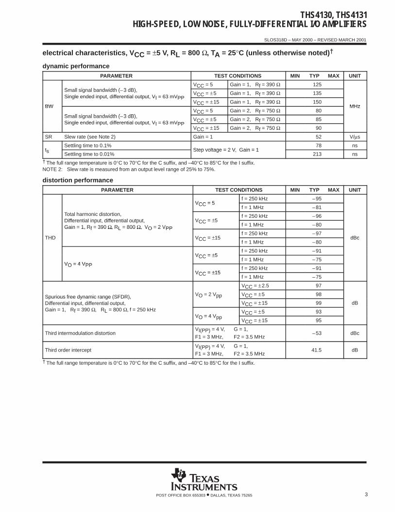
electrical characteristics, VCC = ±5 V, RL = 800 Ω, TA = 25°C (unless otherwise noted)†
dynamic performancePARAMETER TEST CONDITIONS MIN TYP MAX UNIT
BW
Small signal bandwidth (–3 dB),VCC = 5 Gain = 1, Rf = 390 Ω 125
MHzBW
Small signal bandwidth (–3 dB),Single ended input, differential output, VI = 63 mVPP
VCC = ±5 Gain = 1, Rf = 390 Ω 135
MHzBW
Single ended input, differential output, VI = 63 mVPPVCC = ±15 Gain = 1, Rf = 390 Ω 150
MHzBW
Small signal bandwidth (–3 dB),VCC = 5 Gain = 2, Rf = 750 Ω 80
MHz
Small signal bandwidth (–3 dB),Single ended input, differential output, VI = 63 mVPP
VCC = ±5 Gain = 2, Rf = 750 Ω 85Single ended input, differential output, VI = 63 mVPP
VCC = ±15 Gain = 2, Rf = 750 Ω 90
SR Slew rate (see Note 2) Gain = 1 52 V/µs
tsSettling time to 0.1%
Step voltage = 2 V, Gain = 178 ns
ts Settling time to 0.01%Step voltage = 2 V, Gain = 1
213 ns
† The full range temperature is 0°C to 70°C for the C suffix, and –40°C to 85°C for the I suffix.NOTE 2: Slew rate is measured from an output level range of 25% to 75%.
distortion performancePARAMETER TEST CONDITIONS MIN TYP MAX UNIT
THD
Total harmonic distortion,
VCC = 5f = 250 kHz –95
dBcTHD
Total harmonic distortion,
VCC = 5f = 1 MHz –81
dBcTHD
Total harmonic distortion,Differential input, differential output, VCC = ±5
f = 250 kHz –96
dBcTHD
Differential input, differential output,Gain = 1, Rf = 390 Ω, RL = 800 Ω, VO = 2 VPP
VCC = ±5f = 1 MHz –80
dBcTHD
Gain = 1, Rf = 390 Ω, RL = 800 Ω, VO = 2 VPP
VCC = ±15f = 250 kHz –97
dBcTHD VCC = ±15f = 1 MHz –80
dBc
V = 4 V
VCC = ±5f = 250 kHz –91
VO = 4 VPP
VCC = ±5f = 1 MHz –75
VO = 4 VPPVCC = ±15
f = 250 kHz –91VCC = ±15
f = 1 MHz –75
Spurious free dynamic range (SFDR), V = 2 V
VCC = ±2.5 97
dBSpurious free dynamic range (SFDR), VO = 2 Vpp VCC = ±5 98
dBSpurious free dynamic range (SFDR),Differential input, differential output,Gain = 1, R = 390 , R = 800 f = 250 kHz
O ppVCC = ±15 99 dB
Gain = 1, Rf = 390 Ω, RL = 800 Ω, f = 250 kHzVO = 4 Vpp
VCC = ±5 93VO = 4 Vpp
VCC = ±15 95
Third intermodulation distortionVI(PP) = 4 V, G = 1,
F1 = 3 MHz, F2 = 3.5 MHz–53 dBc
Third order interceptVI(PP) = 4 V, G = 1,
F1 = 3 MHz, F2 = 3.5 MHz41.5 dB
† The full range temperature is 0°C to 70°C for the C suffix, and –40°C to 85°C for the I suffix.

THS4130, THS4131HIGH-SPEED, LOW NOISE, FULLY-DIFFERENTIAL I/O AMPLIFIERS
SLOS318D – MAY 2000 – REVISED MARCH 2001
4 POST OFFICE BOX 655303 • DALLAS, TEXAS 75265
electrical characteristics, VCC = ±5 V, RL = 800 Ω, TA = 25°C (unless otherwise noted) (continued)†
noise performancePARAMETER TEST CONDITIONS MIN TYP MAX UNIT
Vn Input voltage noise f = 10 kHz 1.3 nV/√Hz
In Input current noise f = 10 kHz 1 pA/√Hz
† The full range temperature is 0°C to 70°C for the C suffix, and –40°C to 85°C for the I suffix.
dc performancePARAMETER TEST CONDITIONS MIN TYP MAX UNIT
Open loop gainTA = 25°C 71 78
dBOpen loop gainTA = full range 69
dB
V
Input offset voltageTA = 25°C 0.2 2
mVV(OS)
Input offset voltageTA = full range 3 mV
V(OS)Common mode input offset voltage, referred to VOCM TA = 25°C 0.2 3.5
Input offset voltage drift TA = full range 4.5 µV/°C
IIB Input bias current TA = full range 2 6 µA
IOSInput offset current
TA = full range100 500 nA
IOS Offset driftTA = full range
2 nA/°C† The full range temperature is 0°C to 70°C for the C suffix, and –40°C to 85°C for the I suffix.
input characteristicsPARAMETER TEST CONDITIONS MIN TYP MAX UNIT
CMRR Common-mode rejection ratio TA = full range 80 95 dB
VICR Common-mode input voltage range–3.77 –4 to
VVICR Common-mode input voltage range–3.77to 4.3
–4 to4.5
V
RI Input resistance Measured into each input terminal 34 MΩ
CI Input capacitance, closed loop 4 pF
ro Output resistance Open loop 41 Ω† The full range temperature is 0°C to 70°C for the C suffix, and –40°C to 85°C for the I suffix.
output characteristicsPARAMETER TEST CONDITIONS MIN TYP MAX UNIT
Output voltage swing
VCC = 5 VTA = 25°C 1.2 to 3.8 0.9 to 4.1
VOutput voltage swing
VCC = 5 VTA = full range 1.3 to 3.7
VOutput voltage swing VCC = ±5 VTA = 25°C ±3.7 ±4
VOutput voltage swing VCC = ±5 VTA = full range ±3.6
V
VCC = ±15 VTA = 25°C ±10.5 ±12.4
VCC = ±15 VTA = full range ±10.2
I Output current
VCC = 5 V, TA = 25°C 25 45
mAI Output current
VCC = 5 V,RL = 7 Ω TA = full range 20
mAIO Output currentVCC = ±5 V, TA = 25°C 30 55
mAIO Output currentVCC = 5 V,RL = 7 Ω TA = full range 28
mA
VCC = ±15 V, TA = 25°C 60 85VCC = 15 V,RL = 7 Ω TA = full range 50
† The full range temperature is 0°C to 70°C for the C suffix, and –40°C to 85°C for the I suffix.

THS4130, THS4131HIGH-SPEED, LOW NOISE, FULLY-DIFFERENTIAL I/O AMPLIFIERS
SLOS318D – MAY 2000 – REVISED MARCH 2001
5POST OFFICE BOX 655303 • DALLAS, TEXAS 75265
electrical characteristics, VCC = ±5 V, RL = 800 Ω, TA = 25°C (unless otherwise noted) (continued)†
power supplyPARAMETER TEST CONDITIONS MIN TYP MAX UNIT
VCC Supply voltage rangeSingle supply 4 33
VVCC Supply voltage rangeSplit supply ±2 ±16.5
V
I Quiescent currentVCC = ±5 V
TA = 25°C 12.3 15
mAICC Quiescent currentVCC = ±5 V
TA = full range 16 mACCVCC = ±15 V TA = 25°C 14
ICC(SD) Quiescent current (shutdown) (THS4130 only) VPD = –5 VTA = 25°C 0.86 1.4
mAICC(SD) Quiescent current (shutdown) (THS4130 only) VPD = –5 VTA = full range 1.5
mA
PSRR Power supply rejection ratio (dc)TA = 25°C 73 98
dBPSRR Power supply rejection ratio (dc)TA = full range 70
dB
† The full range temperature is 0°C to 70°C for the C suffix, and –40°C to 85°C for the I suffix.
TYPICAL CHARACTERISTICS
Table of GraphsFIGURE
Small signal frequency response 1, 2
Small signal frequency response (various supplies) 3
Small signal frequency response (various CF) 4
Small signal frequency response (various CL) 5
Large signal transient response (differential in/single out) 6
Large signal frequency response 7
CMMR Common mode rejection ratio vs Frequency 8
ICC Supply currentvs Free-air temperature 9
ICC Supply currentvs Free-air temperature (shutdown state) 10
IIB Input bias current vs Free-air temperature 11
Settling time 12
PSRR Power supply rejection ratio vs Frequency (differential out) 13
Large signal transient response 14
THD Total harmonic distortion vs Frequency 15
Second harmonic distortionvs Frequency 16, 17
Second harmonic distortionvs Output voltage 18, 19
Third harmonic distortionvs Frequency 20, 21
Third harmonic distortionvs Output voltage 22, 23
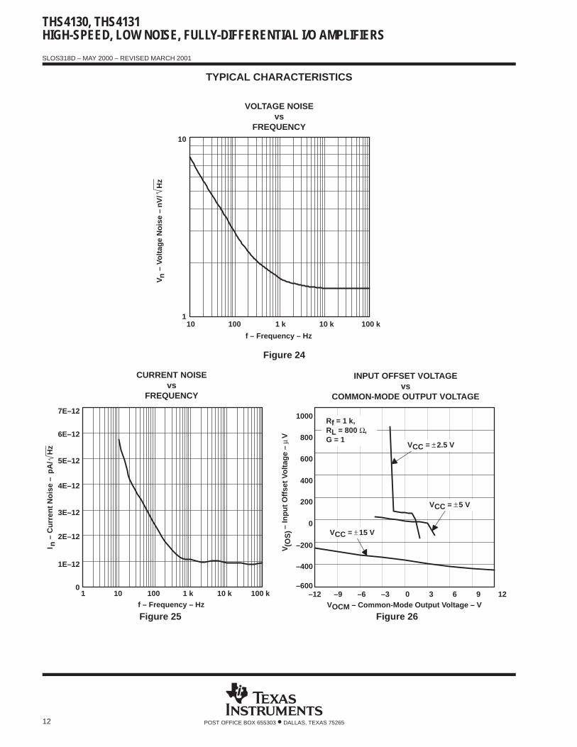
Vn Voltage noise vs Frequency 24
In Current noise vs Frequency 25
V(OS) Input offset voltage vs Common-mode output voltage 26
VO Output voltage vs Differential load resistance 27
zo Output impedance vs Frequency 28

THS4130, THS4131HIGH-SPEED, LOW NOISE, FULLY-DIFFERENTIAL I/O AMPLIFIERS
SLOS318D – MAY 2000 – REVISED MARCH 2001
6 POST OFFICE BOX 655303 • DALLAS, TEXAS 75265
TYPICAL CHARACTERISTICS
Figure 1
–10
–5
0
5
10
15
20
25
100 k 1 M 10 M 100 M 1 Gf – Frequency – Hz
Gain = 5_Rf = 2 kΩ
Gain = 10_Rf = 4 kΩ
Gain = 1_Rf = 390 Ω
Gain = 2_Rf = 750 Ω
RL = 800 Ω,VCC = ±5 V,VI = 63 mVPP
Ou
tpu
t –d
B
SMALL SIGNAL FREQUENCY RESPONSE
Figure 2
–8
–3
2Gain = 1,RL = 800 Ω,VCC = ±5 V,VI = 63 mVPP
100 k 1 M 10 M 100 M 1 Gf – Frequency – Hz
Ou
tpu
t –
dB
SMALL SIGNAL FREQUENCY RESPONSE
3
1
0
–1
–2
–4
–5
–6
–7
Rf = 620 Ω
Rf = 390 Ω
Figure 3
–8
–3
2
100 k 1 M 10 M 100 M 1 Gf – Frequency – Hz
Ou
tpu
t –
dB
SMALL SIGNAL FREQUENCY RESPONSE(VARIOUS SUPPLIES)
VCC= 5
VCC= ±15
Gain = 1,RL = 800 Ω,Rf = 390 Ω,VI = 63 mVPP–7
–6
–5
–4
–2
–1
0
1
Ou
tpu
t –
dB
Figure 4
–10
–5
0
CF = 0 pF
CF = 1 pF
SMALL SIGNAL FREQUENCY RESPONSE(VARIOUS CF)
100 k 1 M 10 M 100 M 1 Gf – Frequency – Hz
–9
–8
–7
–6
–4
–3
–2
–1
1
2
3

THS4130, THS4131HIGH-SPEED, LOW NOISE, FULLY-DIFFERENTIAL I/O AMPLIFIERS
SLOS318D – MAY 2000 – REVISED MARCH 2001
7POST OFFICE BOX 655303 • DALLAS, TEXAS 75265
TYPICAL CHARACTERISTICS
Figure 5
–8
–3
2
CL = 10 pF
SMALL SIGNAL FREQUENCY RESPONSE(VARIOUS CL)
100 k 1 M 10 M 100 M 1 Gf – Frequency – Hz
Ou
tpu
t –
dB
Gain = 1,RL = 800 Ω,VCC = ±5 V,VI = 63 mVPP,Rf = 390 Ω
CL = 0 pF
–7
–6
–5
–4
–2
–1
–0
1
3
4
5
Figure 6
–1
–0.5
0
0.5
–0.5
0
0.5
1
0 0.2 0.4 0.6L
arg
e S
ign
al T
ran
sien
t R
esp
on
se –
V
LARGE SIGNAL TRANSIENT RESPONSE(DIFFERENTIAL IN/SINGLE OUT)
t – Time – µs
VO+
VO–
VI (Diff)
0.1 0.3 0.5
Figure 7
–25
–20
–15
–10
–5
0
5
100 k 10 M 100 M 1 G1 M
VCC = ±5 V
VCC = ±15 V
VCC = 5 V
Gain = 1Rf = 390 Ω,RL = 800 Ω,CF = 0 pF,VI = 0.2 VRMS
Ou
tpu
t –
dB
f – Frequency – Hz
LARGE SIGNAL FREQUENCY RESPONSE
–100
–95
–90
–85
–80
–75
–70
–65
–60
–55
–50
CM
RR
– C
om
mo
n M
od
e R
ejec
tio
n R
atio
– d
B
COMMON MODE REJECTION RATIOvs
FREQUENCY
100 k 1 M 10 M 100 Mf – Frequency – Hz
Rf = 1 kΩ,VCC = ±5 V
Figure 8

THS4130, THS4131HIGH-SPEED, LOW NOISE, FULLY-DIFFERENTIAL I/O AMPLIFIERS
SLOS318D – MAY 2000 – REVISED MARCH 2001
8 POST OFFICE BOX 655303 • DALLAS, TEXAS 75265
TYPICAL CHARACTERISTICS
10
10.5
11
11.5
12
12.5
13
13.5
14
14.5
15
–40 –20 0 20 40 60 80 100
VCC = ±15 V
VCC = ±5 V
– S
up
ply
Cu
rren
t –
mA
SUPPLY CURRENTvs
FREE-AIR TEMPERATURE
I CC
TA – Free-Air Temperature – °C
Figure 9 Figure 10
800
820
840
860
880
900
920
940
–50 –25 0 25 50 75 100
– S
up
ply
Cu
rren
t –
SUPPLY CURRENTvs
FREE-AIR TEMPERATURE (SHUTDOWN STATE)
TA – Free-Air Temperature (Shutdown State) – °C
I CC
Aµ
Figure 11
2.05
2.1
2.15
2.2
2.25
2.3
2.35
2.4
–50 –25 0 25 50 75 100
IIB+
IIB–
INPUT BIAS CURRENTvs
FREE-AIR TEMPERATURE
– In
pu
t B
ias
Cu
rren
t –
I IBA
µ
TA – Free-Air Temperature – °C
Figure 12
1.98
1.96
1.94
1.90 25 50 75
2
2.02
2.04
100 125 150
1.92
RF = 510 ΩCF = 1 pF,VCC = 5 VVO = 4 VPPRL = 800 Ω
– O
utp
ut
Vo
ltag
e –
V
SETTLING TIME
t – Time – ns
VO

THS4130, THS4131HIGH-SPEED, LOW NOISE, FULLY-DIFFERENTIAL I/O AMPLIFIERS
SLOS318D – MAY 2000 – REVISED MARCH 2001
9POST OFFICE BOX 655303 • DALLAS, TEXAS 75265
TYPICAL CHARACTERISTICS
–100
–90
–80
–70
–60
–50
–40
10 k 100 k 1 M 10 M 100 M
VCC = 5 V
VCC = –5 V
PS
RR
– P
ow
er S
up
ply
Rej
ecti
on
Rat
io –
dB
POWER SUPPLY REJECTION RATIOvs
FREQUENCY (DIFFERENTIAL OUT)
f – Frequency (Differential Out) – Hz
Gain = 1,Rf = 330 Ω,RL = 400 Ω
Figure 13 Figure 14
–2.5
–2
–1.5
–1
–5
0
5
1
1.5
2
2.5
0 40 80 120 160 200
VO+
VO–
t – Time – nS
G = 1,Rf = 390 Ω,RL = 800 Ω,CF = 0 pF,CL = 10 pF,VI_Peak = 2 V,VCC = ±15 VTA = 25°C
– O
utp
ut
Vo
ltag
e –
V
LARGE SIGNAL TRANSIENT RESPONSE
VO
–100
–90
–80
–70
–60
–50
–40
–30
–20
100k 1M 10M
VOUT = 2 VPP
VCC = 5 V to ± 5 V
VCC = ± 15 V
Figure 15
TH
D –
To
tal H
arm
on
ic D
isto
rtio
n –
dB
f – Frequency – Hz
TOTAL HARMONIC DISTORTIONvs
FREQUENCY

THS4130, THS4131HIGH-SPEED, LOW NOISE, FULLY-DIFFERENTIAL I/O AMPLIFIERS
SLOS318D – MAY 2000 – REVISED MARCH 2001
10 POST OFFICE BOX 655303 • DALLAS, TEXAS 75265
TYPICAL CHARACTERISTICS
–110
–100
–90
–80
–70
–60
–50
–40
–30
100 k 1 M 10 M
VCC = 5 V
VCC = ±15V, ±5V
Sec
on
d H
arm
on
ic D
isto
rtio
n –
dB
c
f – Frequency – Hz
SECOND HARMONIC DISTORTIONvs
FREQUENCY
VO = 2 VPP,RL = 800 Ω,Rf = 390 Ω,G = 1
Figure 16
Single Ended InputDifferential Output
–110
–100
–90
–80
–70
–60
–50
–40
–30
VCC = ±5 V
VCC = ±15 V
VO = 4 VPP,RL = 800 Ω,Rf = 390 Ω,G = 1
100 k 1 M 10 Mf – Frequency – Hz
SECOND HARMONIC DISTORTIONvs
FREQUENCY
Sec
on
d H
arm
on
ic D
isto
rtio
n –
dB
c
Figure 17
Single Ended InputDifferential Output
Figure 18
Sec
on
d H
arm
on
ic D
isto
rtio
n –
dB
c
–106
–104
–102
–100
–98
–96
–94
–92
0 1 2 3 4 5 6 7
VCC = ±5 V
VCC = ±15 V
f = 250 KHzRL = 800 Ω,Rf = 390 Ω,G = 1
SECOND HARMONIC DISTORTIONvs
OUTPUT VOLTAGE
VO – Output Voltage – V
VCC = 5 V
Single Ended InputDifferential Output
Sec
on
d H
arm
on
ic D
isto
rtio
n –
dB
c
–106
–104
–102
–100
–98
–96
–94
–92
–90
–88
0 1 2 3 4 5 6 7
VCC = ±15 V
VCC = ±5 V
VCC = 5 V
f = 500 KHzRL = 800 Ω,Rf = 390 Ω,G = 1
SECOND HARMONIC DISTORTIONvs
OUTPUT VOLTAGE
VO – Output Voltage – VFigure 19
Single Ended InputDifferential Output

THS4130, THS4131HIGH-SPEED, LOW NOISE, FULLY-DIFFERENTIAL I/O AMPLIFIERS
SLOS318D – MAY 2000 – REVISED MARCH 2001
11POST OFFICE BOX 655303 • DALLAS, TEXAS 75265
TYPICAL CHARACTERISTICS
–110
–100
–90
–80
–70
–60
–50
–40
–30
100 k 1 M 10 M
VCC = ±5 V
VO = 4 VPPRL = 800 Ω,Rf = 390 Ω,G = 1
THIRD HARMONIC DISTORTIONvs
FREQUENCY
f – Frequency – Hz
VCC = ±15 V
Th
ird
Har
mo
nic
Dis
tort
ion
– d
Bc
Figure 20
Single Ended InputDifferential Output
Figure 21
–110
–100
–90
–80
–70
–60
–50
–40
–30
100 k 1 M 10 M
VCC = ±5 V
VCC = ±15 V
VCC = 5 V
VO = 2 VPP,RL = 800 Ω,Rf = 390 Ω,Gain = 1
Th
ird
Har
mo
nic
Dis
tort
ion
– d
Bc
THIRD HARMONIC DISTORTIONvs
FREQUENCY
f – Frequency – Hz
Single Ended InputDifferential Output
Figure 22
–106
–104
–102
–100
–98
–96
–94
–92
–90
–88
0 1 2 3 4 5 6 7
VCC = ±5 V
VCC = 5 V
f = 500 KHzRL = 800 Ω,Rf = 390 Ω,G = 1T
hir
d H
arm
on
ic D
isto
rtio
n –
dB
c
THIRD HARMONIC DISTORTIONvs
OUTPUT VOLTAGE
VO – Output Voltage – V
VCC = ±15 V
Single Ended InputDifferential Output
Th
ird
Har
mo
nic
Dis
tort
ion
– d
Bc
–106
–104
–102
–100
–98
–96
–94
–92
–90
–88
0 1 2 3 4 5 6 7
VCC = 5 V
VCC = ±5 V
f = 250 KHzRL = 800 Ω,Rf = 390 Ω,G = 1
THIRD HARMONIC DISTORTIONvs
OUTPUT VOLTAGE
VO – Output Voltage – V
VCC = ±15 V
Figure 23
Single Ended InputDifferential Output
THS4130, THS4131HIGH-SPEED, LOW NOISE, FULLY-DIFFERENTIAL I/O AMPLIFIERS
SLOS318D – MAY 2000 – REVISED MARCH 2001
12 POST OFFICE BOX 655303 • DALLAS, TEXAS 75265
TYPICAL CHARACTERISTICS
Figure 24
10 100 1 k 10 k 100 k
f – Frequency – Hz
VOLTAGE NOISEvs
FREQUENCY10
nV
/H
z–
Vo
ltag
e N
ois
e –
Vn
1
Figure 25
0
1E–12
2E–12
3E–12
4E–12
5E–12
6E–12
7E–12
1 10 100 1 k 10 k 100 kf – Frequency – Hz
CURRENT NOISEvs
FREQUENCY
I n–
Cu
rren
t N
ois
e –
pA
/H
z
Figure 26
–600
–400
–200
0
200
400
600
800
1000
–12 –9 –6 –3 0 3 6 9 12
– In
pu
t O
ffse
t V
olt
age
–
INPUT OFFSET VOLTAGEvs
COMMON-MODE OUTPUT VOLTAGE
VCC = ±2.5 V
VCC = ±5 V
VCC = ±15 V
V(O
S)
Vµ
VOCM – Common-Mode Output Voltage – V
Rf = 1 k,RL = 800 Ω,G = 1

THS4130, THS4131HIGH-SPEED, LOW NOISE, FULLY-DIFFERENTIAL I/O AMPLIFIERS
SLOS318D – MAY 2000 – REVISED MARCH 2001
13POST OFFICE BOX 655303 • DALLAS, TEXAS 75265
TYPICAL CHARACTERISTICS
–15
–10
–5
0
5
10
15
100 1000 10 k 100 k
OUTPUT VOLTAGEvs
DIFFERENTIAL LOAD RESISTANCE
– O
utp
ut
Vo
ltag
e –
VV
O
RL – Differential Load Resistance – Ω
Rf = 1 kG = 2
Figure 27
VCC = ±15 V
VCC = ±5 V
VCC = ±5 V
VCC = ±15 V
VOUT+
VOUT+
VOUT–
VOUT–
0.1
1
10
100
100 k 1 M 10 M 100 M 1 G
– O
utp
ut
imp
edan
ce –
f – Frequency – Hz
OUTPUT IMPEDANCEvs
FREQUENCY
Ω
VCC = ±5 V
Figure 28
z o

THS4130, THS4131HIGH-SPEED, LOW NOISE, FULLY-DIFFERENTIAL I/O AMPLIFIERS
SLOS318D – MAY 2000 – REVISED MARCH 2001
14 POST OFFICE BOX 655303 • DALLAS, TEXAS 75265
APPLICATION INFORMATION
resistor matching
Resistor matching is important in fully differential amplifiers. The balance of the output on the reference voltagedepends on matched ratios of the resistor. CMRR, PSRR, and cancellation of the second harmonic distortionwill diminish if resistor mismatch occurs. Therefore, it is recommended to use 1% tolerance resistors or betterto keep the performance optimized.
VOCM sets the dc level of the output signals. If no voltage is applied to the VOCM pin, it will be set to the midrailvoltage internally defined as:
VCC VCC–
2
In the differential mode, the VOCM on the two outputs cancel each other. Therefore, the output in the differentialmode is the same as the input in the gain of 1. VOCM has a high bandwidth capability up to the typical operationrange of the amplifier. For the prevention of noise going through the device, use a 0.1 µF capacitor on the VOCMpin as a bypass capacitor. The following graph shows the simplified diagram of the THS413x.
_+
x1
Output Buffer
Vcm ErrorAmplifier
C R
C R
x1
Output Buffer
VOUT+
VOUT–
VCC+
VCC–
VIN–
VIN+
30 kΩ30 kΩ
VCC+
VCC–VOCM
Figure 29. THS413x Simplified Diagram

THS4130, THS4131HIGH-SPEED, LOW NOISE, FULLY-DIFFERENTIAL I/O AMPLIFIERS
SLOS318D – MAY 2000 – REVISED MARCH 2001
15POST OFFICE BOX 655303 • DALLAS, TEXAS 75265
APPLICATION INFORMATION
data converters
Data converters are one of the most popular applications for the fully differential amplifiers. The followingschematic shows a typical configuration of a fully differential amplifier attached to a differential ADC.
VIN
–
+ –
+
DVDDVOCM
AVSS
AVDD
AIN2
AIN1
VDD
Vref
5 V
VCC
0.1 µF
–5 VVCC–
Figure 30. Fully Differential Amplifier Attached to a Differential ADC
Fully differential amplifiers can operate with a single supply. VOCM defaults to the midrail voltage, VCC/2. Thedifferential output may be fed into a data converter. This method eliminates the use of a transformer in the circuit.If the ADC has a reference voltage output (Vref), then it is recommended to connect it directly to the VOCM ofthe amplifier using a bypass capacitor for stability. For proper operation, the input common-mode voltage to theinput terminal of the amplifier should not exceed the common-mode input voltage range.
VIN
–
+ –
+
DVDDVOCM
AVSS
AVDD
AIN2
AIN1
VDD
Vref
5 V
VCC
0.1 µF
Figure 31. Fully Differential Amplifier Using a Single Supply

THS4130, THS4131HIGH-SPEED, LOW NOISE, FULLY-DIFFERENTIAL I/O AMPLIFIERS
SLOS318D – MAY 2000 – REVISED MARCH 2001
16 POST OFFICE BOX 655303 • DALLAS, TEXAS 75265
APPLICATION INFORMATION
data converters (continued)
Some single supply applications may require the input voltage to exceed the common-mode input voltagerange. In such cases, the following circuit configuration is suggested to bring the common-mode input voltagewithin the specifications of the amplifier.
VIN
–
+ –
+
DVDDVOCM
AVSS
AVDD
AIN2
AIN1
VDD
Vref
5 V
VCC
0.1 µF
RPU
RPU
THS1206
VCC Rf
Rg
VCC Rf
Rg
VP
VOUT
VOUT
Figure 32. Circuit With Improved Common-Mode Input Voltage
The following equation is used to calculate RPU:
RPU VP – VCC
VIN – VP 1
RG VOUT – VP
1RF
driving a capacitive load
Driving capacitive loads with high performance amplifiers is not a problem as long as certain precautions aretaken. The first is to realize that the THS413x has been internally compensated to maximize its bandwidth andslew rate performance. When the amplifier is compensated in this manner, capacitive loading directly on theoutput will decrease the device’s phase margin leading to high frequency ringing or oscillations. Therefore, forcapacitive loads of greater than 10 pF, it is recommended that a resistor be placed in series with the output ofthe amplifier, as shown in Figure 33. A minimum value of 20 Ω should work well for most applications. Forexample, in 50-Ω transmission systems, setting the series resistor value to 50 Ω both isolates any capacitanceloading and provides the proper line impedance matching at the source end.
THS413x
Output
Output
20 Ω
20 Ω
390 Ω
390 Ω
390 Ω
390 Ω
Figure 33. Driving a Capacitive Load
THS4130, THS4131HIGH-SPEED, LOW NOISE, FULLY-DIFFERENTIAL I/O AMPLIFIERS
SLOS318D – MAY 2000 – REVISED MARCH 2001
17POST OFFICE BOX 655303 • DALLAS, TEXAS 75265
APPLICATION INFORMATION
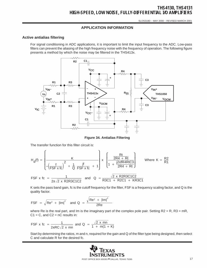
Active antialias filtering
For signal conditioning in ADC applications, it is important to limit the input frequency to the ADC. Low-passfilters can prevent the aliasing of the high frequency noise with the frequency of operation. The following figurepresents a method by which the noise may be filtered in the THS413x.
VIN–
VIN+ +
– +
–
VOCM
VOCMVIN–
VIN+
VCC–
THS1050THS413x
C3
C3
R4
R(t)
R2
R4
+C1
+
VCC
C1R2
R3
R3
C2
R1
R1
Vs
VIC
Figure 34. Antialias Filtering
The transfer function for this filter circuit is:
Hd(f)
K
– fFSF x fc
2 1Q
jfFSF x fc
1
x
Rt2R4 Rt
1 j2πfR4RtC32R4 Rt
Where K R2
R1
FSF x fc 12π 2 x R2R3C1C2 and Q 2 x R2R3C1C2
R3C1 R2C1 KR3C1
K sets the pass band gain, fc is the cutoff frequency for the filter, FSF is a frequency scaling factor, and Q is thequality factor.
FSF Re2 |Im|2 and Q
Re2 |Im|2
2Re
where Re is the real part, and Im is the imaginary part of the complex pole pair. Setting R2 = R, R3 = mR, C1 = C, and C2 = nC results in:
FSF x fc 12πRC 2 x mn and Q 2 x mn
1 m(1 K)
Start by determining the ratios, m and n, required for the gain and Q of the filter type being designed, then selectC and calculate R for the desired fc.
THS4130, THS4131HIGH-SPEED, LOW NOISE, FULLY-DIFFERENTIAL I/O AMPLIFIERS
SLOS318D – MAY 2000 – REVISED MARCH 2001
18 POST OFFICE BOX 655303 • DALLAS, TEXAS 75265
PRINCIPLES OF OPERATION
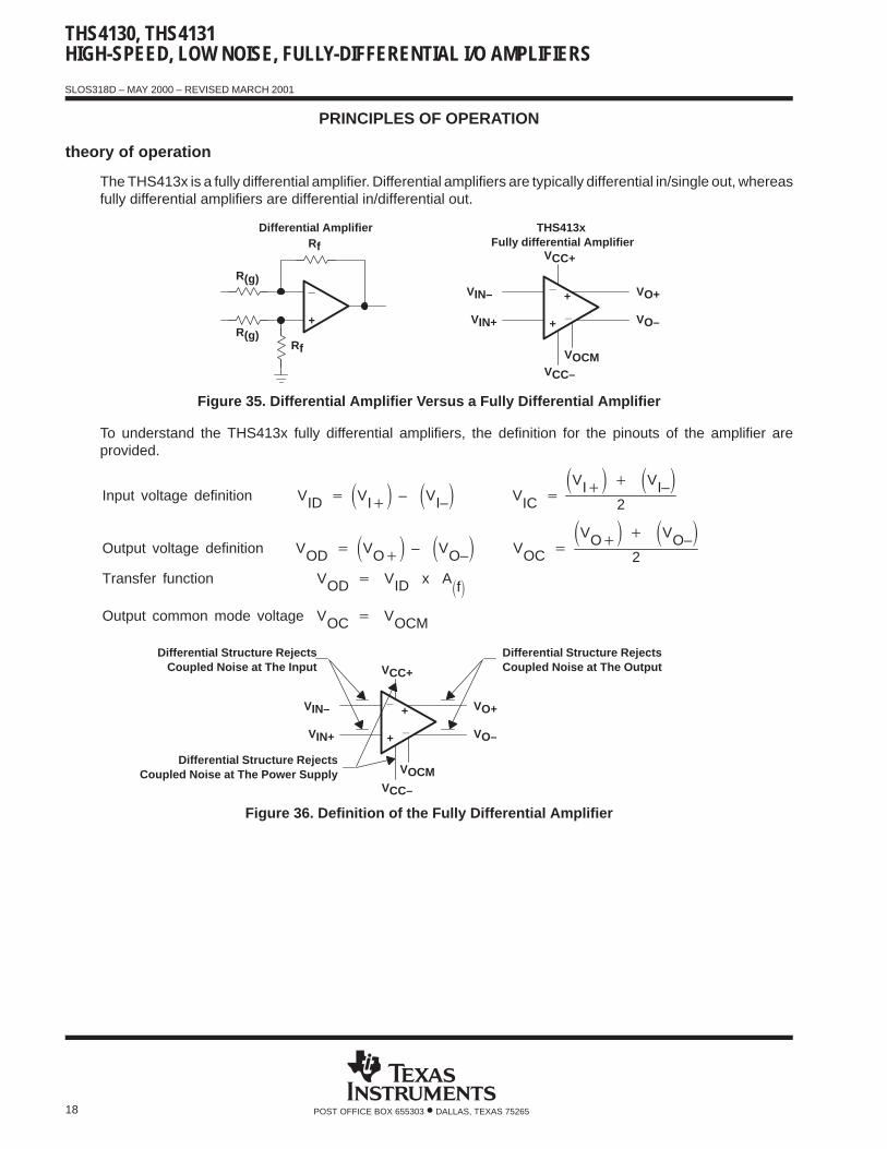
theory of operation
The THS413x is a fully differential amplifier. Differential amplifiers are typically differential in/single out, whereasfully differential amplifiers are differential in/differential out.
Rf
R(g)
R(g)Rf
_
+
Differential Amplifier
VOCM
_
+_
+
VCC+
VIN–
VIN+
VO+
VO–
THS413x Fully differential Amplifier
VCC–
Figure 35. Differential Amplifier Versus a Fully Differential Amplifier
To understand the THS413x fully differential amplifiers, the definition for the pinouts of the amplifier areprovided.
Input voltage definition VID VI – VI–
VIC VI
VI–
2
Output voltage definition VOD VO – VO–
VOC VO
VO–
2
Transfer function VOD VID x Af
Output common mode voltage VOC VOCM
VOCM
_
+_
+
VCC+
VIN–
VIN+
VO+
VO–
Differential Structure RejectsCoupled Noise at The Output
Differential Structure RejectsCoupled Noise at The Input
Differential Structure RejectsCoupled Noise at The Power Supply
VCC–
Figure 36. Definition of the Fully Differential Amplifier

THS4130, THS4131HIGH-SPEED, LOW NOISE, FULLY-DIFFERENTIAL I/O AMPLIFIERS
SLOS318D – MAY 2000 – REVISED MARCH 2001
19POST OFFICE BOX 655303 • DALLAS, TEXAS 75265
PRINCIPLES OF OPERATION
theory of operation (continued)
The following schematics depict the differences between the operation of the THS413x, fully differentialamplifier, in two different modes. Fully differential amplifiers can work with differential input or can beimplemented as single in/differential out.
–
Rf
R(g)
+
+
–
VCC–
VCC+
R(g)
Rf
Vs
VIN–
VIN+
VO+
VO–VOCM
Note: For proper operation, maintain symmetry by setting Rf1 = Rf2 = Rf and R(g)1 = R(g)2 = R(g) ⇒ A = Rf/R(g)
Figure 37. Amplifying Differential Signals
–
Rf
R(g)
+
+
–
VCC–
VCC+
R(g)
Rf
Vs
VIN–
VIN+
VO+
VO–VOCM
GAIN R(g) Ω Rf Ω
12510
390374402402
39075020104020
RECOMMENDED RESISTOR VALUES
Figure 38. Single In With Differential Out
If each output is measured independently, each output is one-half of the input signal when gain is 1. Thefollowing equations express the transfer function for each output:
VO
12
VI
The second output is equal and opposite in sign:
VO – 12
VI
THS4130, THS4131HIGH-SPEED, LOW NOISE, FULLY-DIFFERENTIAL I/O AMPLIFIERS
SLOS318D – MAY 2000 – REVISED MARCH 2001
20 POST OFFICE BOX 655303 • DALLAS, TEXAS 75265
PRINCIPLES OF OPERATION
theory of operation (continued)
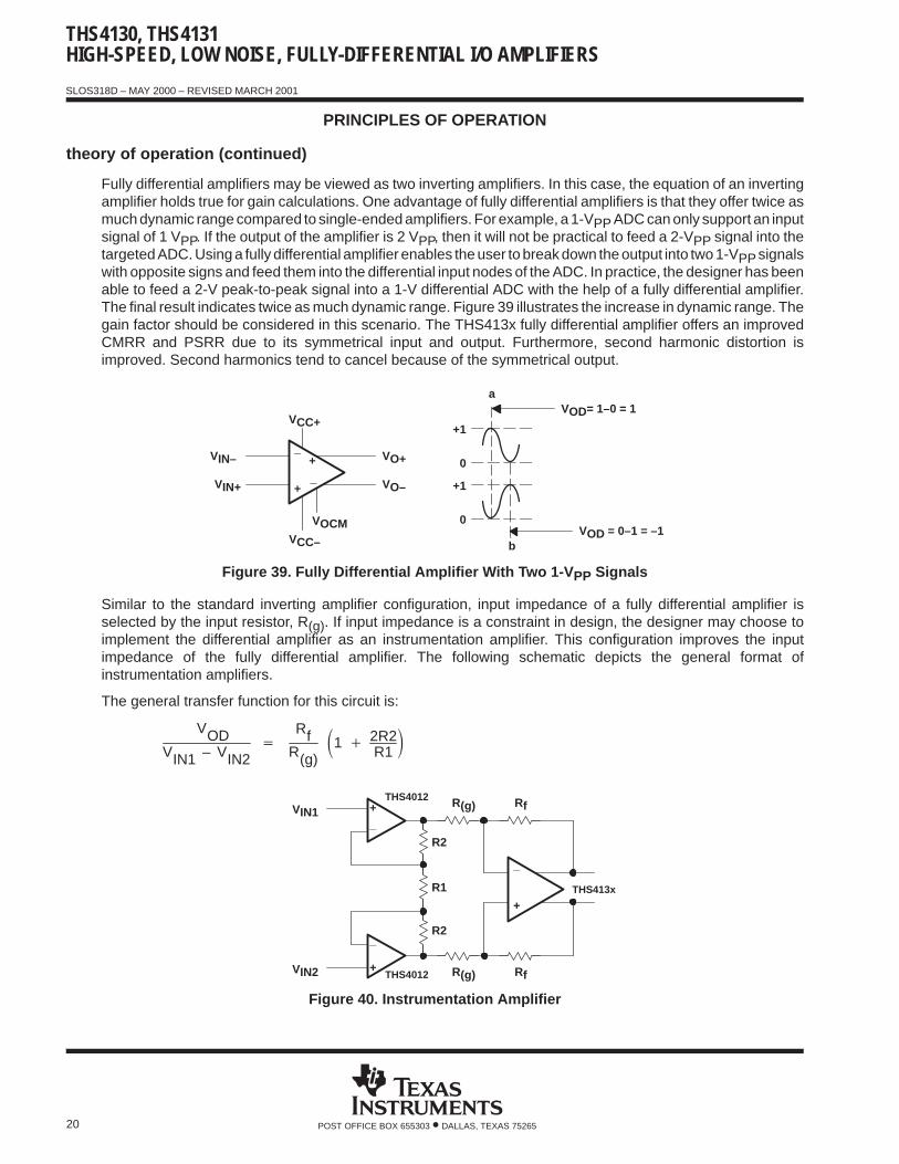
Fully differential amplifiers may be viewed as two inverting amplifiers. In this case, the equation of an invertingamplifier holds true for gain calculations. One advantage of fully differential amplifiers is that they offer twice asmuch dynamic range compared to single-ended amplifiers. For example, a 1-VPP ADC can only support an inputsignal of 1 VPP. If the output of the amplifier is 2 VPP, then it will not be practical to feed a 2-VPP signal into thetargeted ADC. Using a fully differential amplifier enables the user to break down the output into two 1-VPP signalswith opposite signs and feed them into the differential input nodes of the ADC. In practice, the designer has beenable to feed a 2-V peak-to-peak signal into a 1-V differential ADC with the help of a fully differential amplifier.The final result indicates twice as much dynamic range. Figure 39 illustrates the increase in dynamic range. Thegain factor should be considered in this scenario. The THS413x fully differential amplifier offers an improvedCMRR and PSRR due to its symmetrical input and output. Furthermore, second harmonic distortion isimproved. Second harmonics tend to cancel because of the symmetrical output.
VOCM
_
+_
+
VCC+
VIN–
VIN+
VO+
VO–
VOD= 1–0 = 1
VOD = 0–1 = –1
a
b
+1
0
+1
0
VCC–
Figure 39. Fully Differential Amplifier With Two 1-VPP Signals
Similar to the standard inverting amplifier configuration, input impedance of a fully differential amplifier isselected by the input resistor, R(g). If input impedance is a constraint in design, the designer may choose toimplement the differential amplifier as an instrumentation amplifier. This configuration improves the inputimpedance of the fully differential amplifier. The following schematic depicts the general format ofinstrumentation amplifiers.
The general transfer function for this circuit is:
VODVIN1 – VIN2
RfR(g)
1 2R2R1
_
+
_+
_
+
THS4012
THS4012
VIN1
VIN2
R2
R1
R2
R(g)
R(g)
Rf
Rf
THS413x
Figure 40. Instrumentation Amplifier

THS4130, THS4131HIGH-SPEED, LOW NOISE, FULLY-DIFFERENTIAL I/O AMPLIFIERS
SLOS318D – MAY 2000 – REVISED MARCH 2001
21POST OFFICE BOX 655303 • DALLAS, TEXAS 75265
PRINCIPLES OF OPERATION
circuit layout considerations
To achieve the levels of high frequency performance of the THS413x, follow proper printed-circuit board highfrequency design techniques. A general set of guidelines is given below. In addition, a THS413x evaluationboard is available to use as a guide for layout or for evaluating the device performance.
Ground planes—It is highly recommended that a ground plane be used on the board to provide allcomponents with a low inductive ground connection. However, in the areas of the amplifier inputs andoutput, the ground plane can be removed to minimize the stray capacitance.
Proper power supply decoupling—Use a 6.8-µF tantalum capacitor in parallel with a 0.1-µF ceramiccapacitor on each supply terminal. It may be possible to share the tantalum among several amplifiersdepending on the application, but a 0.1-µF ceramic capacitor should always be used on the supply terminalof every amplifier. In addition, the 0.1-µF capacitor should be placed as close as possible to the supplyterminal. As this distance increases, the inductance in the connecting trace makes the capacitor lesseffective. The designer should strive for distances of less than 0.1 inches between the device powerterminals and the ceramic capacitors.
Sockets—Sockets are not recommended for high-speed operational amplifiers. The additional leadinductance in the socket pins will often lead to stability problems. Surface-mount packages soldered directlyto the printed-circuit board is the best implementation.
Short trace runs/compact part placements—Optimum high frequency performance is achieved when strayseries inductance has been minimized. To realize this, the circuit layout should be made as compact aspossible, thereby minimizing the length of all trace runs. Particular attention should be paid to the invertinginput of the amplifier. Its length should be kept as short as possible. This will help to minimize straycapacitance at the input of the amplifier.
Surface-mount passive components—Using surface-mount passive components is recommended for highfrequency amplifier circuits for several reasons. First, because of the extremely low lead inductance ofsurface-mount components, the problem with stray series inductance is greatly reduced. Second, the smallsize of surface-mount components naturally leads to a more compact layout thereby minimizing both strayinductance and capacitance. If leaded components are used, it is recommended that the lead lengths bekept as short as possible.

THS4130, THS4131HIGH-SPEED, LOW NOISE, FULLY-DIFFERENTIAL I/O AMPLIFIERS
SLOS318D – MAY 2000 – REVISED MARCH 2001
22 POST OFFICE BOX 655303 • DALLAS, TEXAS 75265
PRINCIPLES OF OPERATION
power-down mode
The power-down mode is used when power saving is required. The power-down terminal (PD) found on theTHS413x is an active low terminal. If it is left as a no-connect terminal, the device will always stay on due to aninternal 50 kΩ resistor to VCC. The threshold voltage for this terminal is approximately 1.4 V above VCC–. Thismeans that if the PD terminal is 1.4 V above VCC–, the device is active. If the PD terminal is less than 1.4 V aboveVCC–, the device is off. For example, if VCC– = –5 V, then the device is on when PD reaches –3.6 V, (–5 V +1.4 V = –3.6 V). By the same calculation, the device is off below –3.6 V. It is recommended to pull the terminalto VCC– in order to turn the device off. The following graph shows the simplified version of the power-downcircuit. While in the power-down state, the amplifier goes into a high impedance state. The amplifier outputimpedance is typically greater than 1 MΩ in the power-down state.
VCC
PD
VCC–
To Internal BiasCircuitry Control
50 kΩ
Figure 41. Simplified Power-Down Circuit
Due to the similarity of the standard inverting amplifier configuration, the output impedance appears to be verylow while in the power-down state. This is because the feedback resistor (Rf) and the gain resistor (R(g)) arestill connected to the circuit. Therefore, a current path is allowed between the input of the amplifier and the outputof the amplifier. An example of the closed loop output impedance is shown in Figure 42.
Figure 42
200
1200
2200
100 k 1 M 10 M 100 M 1 G
Ou
tpu
t Im
ped
ance
–
f – Frequency – Hz
OUTPUT IMPEDANCE (IN POWER DOWN)vs
FREQUENCY
Ω
VCC = ±5 VG = 1Rf = 1 kΩPD = VCC–

THS4130, THS4131HIGH-SPEED, LOW NOISE, FULLY-DIFFERENTIAL I/O AMPLIFIERS
SLOS318D – MAY 2000 – REVISED MARCH 2001
23POST OFFICE BOX 655303 • DALLAS, TEXAS 75265
PRINCIPLES OF OPERATION
general PowerPAD design considerations
The THS413x is available packaged in a thermally-enhanced DGN package, which is a member of thePowerPAD family of packages. This package is constructed using a downset leadframe upon which the die ismounted [see Figure 43(a) and Figure 43(b)]. This arrangement results in the lead frame being exposed as athermal pad on the underside of the package [see Figure 43(c)]. Because this thermal pad has direct thermalcontact with the die, excellent thermal performance can be achieved by providing a good thermal path awayfrom the thermal pad.
The PowerPAD package allows for both assembly and thermal management in one manufacturing operation.During the surface-mount solder operation (when the leads are being soldered), the thermal pad can also besoldered to a copper area underneath the package. Through the use of thermal paths within this copper area,heat can be conducted away from the package into either a ground plane or other heat dissipating device.
The PowerPAD package represents a breakthrough in combining the small area and ease of assembly of thesurface mount with the, heretofore, awkward mechanical methods of heatsinking.
More complete details of the PowerPAD installation process and thermal management techniques can be foundin the Texas Instruments Technical Brief, PowerPAD Thermally Enhanced Package (SLMA002). This documentcan be found at the TI web site (www.ti.com) by searching on the key word PowerPAD. The document can alsobe ordered through your local TI sales office. Refer to literature number SLMA002 when ordering.
DIE
Side View (a)
End View (b) Bottom View (c)
DIE
ThermalPad
NOTE A: The thermal pad is electrically isolated from all terminals in the package.
Figure 43. Views of Thermally Enhanced DGN Package

THS4130, THS4131HIGH-SPEED, LOW NOISE, FULLY-DIFFERENTIAL I/O AMPLIFIERS
SLOS318D – MAY 2000 – REVISED MARCH 2001
24 POST OFFICE BOX 655303 • DALLAS, TEXAS 75265
MECHANICAL DATAD (R-PDSO-G**) PLASTIC SMALL-OUTLINE PACKAGE14 PINS SHOWN
4040047/D 10/96
0.228 (5,80)0.244 (6,20)
0.069 (1,75) MAX0.010 (0,25)0.004 (0,10)
1
14
0.014 (0,35)0.020 (0,51)
A
0.157 (4,00)0.150 (3,81)
7
8
0.044 (1,12)0.016 (0,40)
Seating Plane
0.010 (0,25)
PINS **
0.008 (0,20) NOM
A MIN
A MAX
DIM
Gage Plane
0.189(4,80)
(5,00)0.197
8
(8,55)
(8,75)
0.337
14
0.344
(9,80)
16
0.394(10,00)
0.386
0.004 (0,10)
M0.010 (0,25)
0.050 (1,27)
0°–8°
NOTES: A. All linear dimensions are in inches (millimeters).B. This drawing is subject to change without notice.C. Body dimensions do not include mold flash or protrusion, not to exceed 0.006 (0,15).D. Falls within JEDEC MS-012

THS4130, THS4131HIGH-SPEED, LOW NOISE, FULLY-DIFFERENTIAL I/O AMPLIFIERS
SLOS318D – MAY 2000 – REVISED MARCH 2001
25POST OFFICE BOX 655303 • DALLAS, TEXAS 75265
MECHANICAL DATADGN (S-PDSO-G8) PowerPAD PLASTIC SMALL-OUTLINE PACKAGE
0,690,41
0,25
Thermal Pad(See Note D)
0,15 NOM
Gage Plane
4073271/A 04/98
4,98
0,25
5
3,054,782,95
8
4
3,052,95
1
0,38
0,150,05
1,07 MAX
Seating Plane
0,10
0,65 M0,25
0°–6°
NOTES: A. All linear dimensions are in millimeters.B. This drawing is subject to change without notice.C. Body dimensions include mold flash or protrusions.D. The package thermal performance may be enhanced by attaching an external heat sink to the thermal pad.
This pad is electrically and thermally connected to the backside of the die and possibly selected leads.E. Falls within JEDEC MO-187
PowerPAD is a trademark of Texas Instruments.

IMPORTANT NOTICE
Texas Instruments Incorporated and its subsidiaries (TI) reserve the right to make corrections, modifications,enhancements, improvements, and other changes to its products and services at any time and to discontinueany product or service without notice. Customers should obtain the latest relevant information before placingorders and should verify that such information is current and complete. All products are sold subject to TI’s termsand conditions of sale supplied at the time of order acknowledgment.
TI warrants performance of its hardware products to the specifications applicable at the time of sale inaccordance with TI’s standard warranty. Testing and other quality control techniques are used to the extent TIdeems necessary to support this warranty. Except where mandated by government requirements, testing of allparameters of each product is not necessarily performed.
TI assumes no liability for applications assistance or customer product design. Customers are responsible fortheir products and applications using TI components. To minimize the risks associated with customer productsand applications, customers should provide adequate design and operating safeguards.
TI does not warrant or represent that any license, either express or implied, is granted under any TI patent right,copyright, mask work right, or other TI intellectual property right relating to any combination, machine, or processin which TI products or services are used. Information published by TI regarding third-party products or servicesdoes not constitute a license from TI to use such products or services or a warranty or endorsement thereof.Use of such information may require a license from a third party under the patents or other intellectual propertyof the third party, or a license from TI under the patents or other intellectual property of TI.
Reproduction of information in TI data books or data sheets is permissible only if reproduction is withoutalteration and is accompanied by all associated warranties, conditions, limitations, and notices. Reproductionof this information with alteration is an unfair and deceptive business practice. TI is not responsible or liable forsuch altered documentation.
Resale of TI products or services with statements different from or beyond the parameters stated by TI for thatproduct or service voids all express and any implied warranties for the associated TI product or service andis an unfair and deceptive business practice. TI is not responsible or liable for any such statements.
Following are URLs where you can obtain information on other Texas Instruments products and applicationsolutions:
Products Applications
Amplifiers amplifier.ti.com Audio www.ti.com/audio
Data Converters dataconverter.ti.com Automotive www.ti.com/automotive
DSP dsp.ti.com Broadband www.ti.com/broadband
Interface interface.ti.com Digital Control www.ti.com/digitalcontrol
Logic logic.ti.com Military www.ti.com/military
Power Mgmt power.ti.com Optical Networking www.ti.com/opticalnetwork
Microcontrollers microcontroller.ti.com Security www.ti.com/security
Telephony www.ti.com/telephony
Video & Imaging www.ti.com/video
Wireless www.ti.com/wireless
Mailing Address: Texas Instruments
Post Office Box 655303 Dallas, Texas 75265
Copyright 2003, Texas Instruments Incorporated


![LMS-T540H英文 1.png · LMS-30 Inductive Load Circuit Vcc OUT More than + 24V Vcc I Vcc 2 * In case of single voltage, VCCI= l.-r.as] USE. CAUTION ON HANDLING Computer Peripharels](https://img.pdfslide.net/doc/110x75/5fb22eb578de9424234c41eb/lms-t540he-1-lms-30-inductive-load-circuit-vcc-out-more-than-24v-vcc-i-vcc.jpg)