Embed Size (px)
Citation preview
TIDUAS1 - November 2015 IEC ESD, EFT, and Surge RS-485 Bus Protection 1
Copyright © 2015, Texas Instruments Incorporated
TI Designs: TIDA-00731
IEC ESD, EFT, and Surge RS-485 Bus Protection
TI Designs
TI Designs provide the foundation that you need including methodology, testing and design files to quickly evaluate and customize the system. TI Designs help you accelerate your time to market.
Design Resources
SN65HVD82 Product Folder
SN65HVD3082E Product Folder
SLLS292A Application Report
Block Diagram
Design Features
Board Level IEC ESD, EFT, and Surge Evaluation
Easy control of transceivers logic I/O pins
PAD Site Evaluation Of Multiple TVS Diode Structures
Series Pulse Proof Resistor Pads
Bourns TBU High Speed Protection Component Evaluation
Bourns Radial Leaded Varistor Protection Evaluation
General Purpose Evaluation Module For Half-Duplex RS-485 Transceivers
Featured Applications
E-Meters
Industrial Automation
Security and Surveillance Equipment
Encoders and Decoders
Board Image
Ask The Analog Experts WEBENCH® Design Center

www.ti.com
Design Overview 1
Industrial networks such as RS-485, RS-422, RS-232, CAN, and Profibus are expected to withstand harsh system-level transients in their end applications without being damaged. These events can be caused by electrostatic discharge during handling, interruption of inductive loads, relay contact bounce, and/or lightning strikes. Designing to meet these requirements can be challenging without the proper tools and knowledge about the standards that the design requires. TI design TIDA-00731 shows a practical example of how to protect the most sensitive components against these lethal transients. This documentation walks through the TIA/EIA-485 standard, the IEC 61000-4-x transient test standards, the implementation of system level protection against the transient and overall schematic design/layout.
www.ti.com
TIDUAS1 - November 2015 IEC ESD, EFT, and Surge RS-485 Bus Protection 3
Copyright © 2015, Texas Instruments Incorporated
Standards 2
There are many standards that can be referenced by engineers looking to ensure ESD robustness in their end design. Human Body Model (HBM), Machine Model (MM), and Charged Device Model (CDM) are the most common ESD standards in industry, as most vendors provide data on these parameters in the supporting documentation for a given device. These traditional ESD models do not take into account system-level ESD events and are solely meant as device level specs. These specifications ensure that the device can make it through the handling and assembly process without being damaged by ESD.
HBM, MM, and CDM are sufficient models for many applications, but some industrial applications are subjected too much greater stresses than the energy levels that these standards deliver. The next three sections will discuss the IEC 61000-4-2 Electrostatic Discharge Immunity Test, IEC 61000-4-4 Electrical Fast Transient/Burst Immunity Test, the IEC 61000-4-5 Surge Immunity Test standards and the expected levels of energy the industrial system can see.
IEC 61000-4-2 Electrostatic Discharge Immunity Test 2.1
The IEC 61000-4-2 ESD immunity test is a system-level ESD test that imitates a charged operator discharging onto an end system. The characteristics of the IEC ESD test differ from that of other ESD standards in rise times, the amount of energy delivered during the strike, and the number of strikes administered during the testing. There are two types of testing methods involved with the IEC ESD: contact discharge and air discharge. The contact ESD test discharges an ESD pulse from an IEC ESD gun directly onto the device under test (DUT). The air ESD discharge test involves moving the charged ESD gun towards the DUT until the air breaks down enough to allow conduction of the ESD strike between the ESD gun and the DUT. The IEC ESD testing is performed with both positive and negative polarities, and a passing score is not achieved unless both polarities at a single level are survived. Table 1 shows the IEC 61000-4-2 ESD test voltage levels and the peak current levels:
Table 1: IEC 61000-4-2 ESD Test Voltage Levels
Contact Discharge Air Discharge
Level Test Voltage (kV) Peak Current (A)
Level Test Voltage (kV)
1 2 7.5 1 2 2 4 15 2 4 3 6 22.5 3 8 4 8 30 4 15 * Special Special * Special
* is an open level. The level has to be specified in the dedicated equipment speciation. If higher voltages than those shown are specified, special test equipment may be needed.
Figure 1 depicts the basic shape of the IEC ESD pulse and shows the timing sequence of the test pulses.

www.ti.com
TIDUAS1 - November 2015 IEC ESD, EFT, and Surge RS-485 Bus Protection 4
Copyright © 2015, Texas Instruments Incorporated
Figure 1: Current Waveform of IEC ESD Pulse and Timing Sequence of Test
IEC 61000-4-4 Electrical Fast Transient/Burst Immunity Test 2.2
The IEC 61000-4-4 electrical fast transient (EFT) or burst immunity test is meant to simulate the switching transients caused by the interruption of inductive loads, relay contact bounce, etc. The EFT test is performed on power lines, I/O data lines, I/O control lines and earth wires. The EFT test is a burst of pulses that have predetermined amplitude and limited duration. The typical duration of a burst is 15 ms at a repetition rate of 5 kHz, although 100 kHz repetition is a more realistic test. The burst period, which is the time from the start of one burst to the start of the next burst, is 300 ms. The test requires the application of six burst frames of ten seconds duration with ten second pauses between frames. In a typical EFT test sequence 3 million pulses will be delivered to the DUT via a capacitive clamp which couples the energy into the system. Table 2 shows the IEC 61000-4-4 EFT test voltage levels and repetition rates:
Table 2: IEC 61000-4-2 ESD Test Voltage Levels
On Power Port, PE On I/O Signal, data and control ports
Level Test Voltage (kV) Repetition Rate (kHz)
Test Voltage (kV)
Repetition Rate (kHz)
1 0.5 5 or 100 0.25 5 or 100 2 1 5 or 100 0.5 5 or 100 3 2 5 or 100 1 5 or 100 4 4 5 or 100 2 5 or 100 * Special Special * Special
*Is an open level. The level has to be specified in the dedicated equipment specification.
Figure 2 depicts the basic shape of the IEC EFT pulse and shows the timing sequence of the test pulses.
Figure 2: Voltage waveform of an EFT (Burst) Pulse and Timing Sequence of an Entire Test Cycle
www.ti.com
TIDUAS1 - November 2015 IEC ESD, EFT, and Surge RS-485 Bus Protection 5
Copyright © 2015, Texas Instruments Incorporated
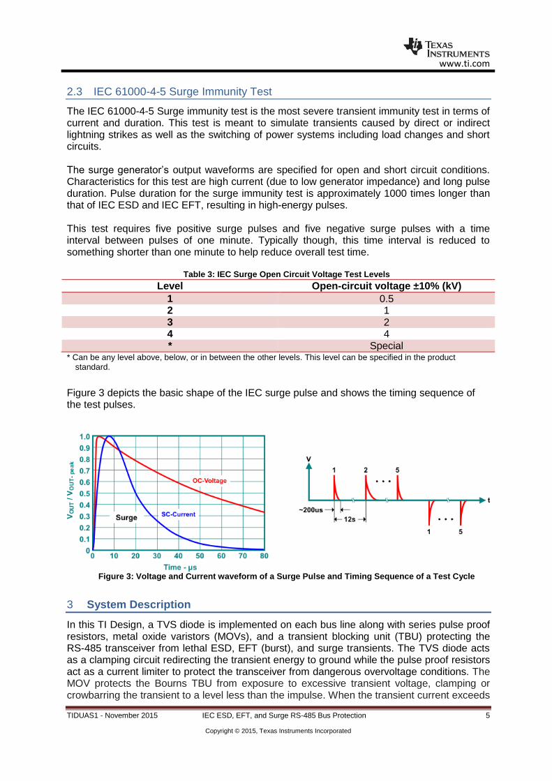
IEC 61000-4-5 Surge Immunity Test 2.3
The IEC 61000-4-5 Surge immunity test is the most severe transient immunity test in terms of current and duration. This test is meant to simulate transients caused by direct or indirect lightning strikes as well as the switching of power systems including load changes and short circuits. The surge generator’s output waveforms are specified for open and short circuit conditions. Characteristics for this test are high current (due to low generator impedance) and long pulse duration. Pulse duration for the surge immunity test is approximately 1000 times longer than that of IEC ESD and IEC EFT, resulting in high-energy pulses. This test requires five positive surge pulses and five negative surge pulses with a time interval between pulses of one minute. Typically though, this time interval is reduced to something shorter than one minute to help reduce overall test time.
Table 3: IEC Surge Open Circuit Voltage Test Levels
Level Open-circuit voltage ±10% (kV)
1 0.5 2 1 3 2 4 4 * Special
* Can be any level above, below, or in between the other levels. This level can be specified in the product standard.
Figure 3 depicts the basic shape of the IEC surge pulse and shows the timing sequence of the test pulses.
Figure 3: Voltage and Current waveform of a Surge Pulse and Timing Sequence of a Test Cycle
System Description 3
In this TI Design, a TVS diode is implemented on each bus line along with series pulse proof resistors, metal oxide varistors (MOVs), and a transient blocking unit (TBU) protecting the RS-485 transceiver from lethal ESD, EFT (burst), and surge transients. The TVS diode acts as a clamping circuit redirecting the transient energy to ground while the pulse proof resistors act as a current limiter to protect the transceiver from dangerous overvoltage conditions. The MOV protects the Bourns TBU from exposure to excessive transient voltage, clamping or crowbarring the transient to a level less than the impulse. When the transient current exceeds

www.ti.com
TIDUAS1 - November 2015 IEC ESD, EFT, and Surge RS-485 Bus Protection 6
Copyright © 2015, Texas Instruments Incorporated
the TBU trigger current limit, the sub-microsecond response of the TBU limits the current flow to the transceiver. The MOV reduces the transients to a few hundred volts of clamping voltage while the TBUs limit transient current to less than 1 mA. Figure 4 shows the TI Design with all of its components:
Figure 4: RS-485 Transceiver with TVS Diode, Series Pulse Proof Resistors, MOV, and TBU MOSFETs
TIA/EIA-485 Standard and Transceivers 4
TIA/EIA-485 Standard 4.1
TIA/EIA-485 is a differential signaling standard which defines the electrical characteristics of drivers and receivers used to implement a balanced, multi-point transmission line. A compliant TIA/EIA-485 transceiver must support a differential signal of 1.5 V across a 54 Ω load as well as a -7 V-to-+12 V common mode voltage range. RS-485 transceivers are designed to support a wide range of serial data transmission data rates over very long distances (up to ~1000 meters). Texas Instruments RS-485 transceivers meet or exceed the requirements set by the TIA/EIA-485 standard and support other features like automatic polarity correction, receiver equalization, 1.8 V I/O levels, and integrated IEC ESD protection. While all of these features are nice to have, this TI Design only focuses on the SN65HVD3082E (a standard 5-V RS-485 transceiver), and the SN65HVD82 (a 5-V transceiver with integrated IEC ESD protection).
4.1.1 SN65HVD3082E
The SN65HVD308xE family of transceivers support half-duplex operation and are designed for RS-485 data bus networks. They are powered by a 5-V supply, support data rates up to 20 Mbps, and are fully compliant to the TIA/EIA-485 standard.
4.1.2 SN65HVD82
www.ti.com
TIDUAS1 - November 2015 IEC ESD, EFT, and Surge RS-485 Bus Protection 7
Copyright © 2015, Texas Instruments Incorporated
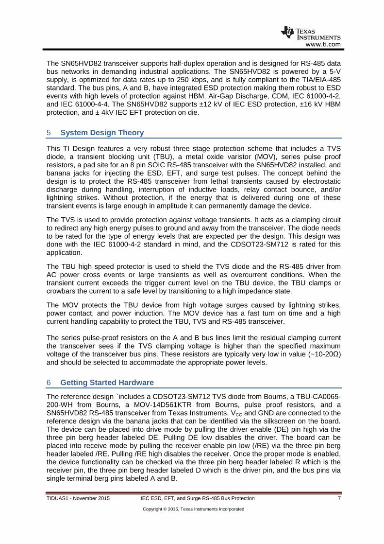
The SN65HVD82 transceiver supports half-duplex operation and is designed for RS-485 data bus networks in demanding industrial applications. The SN65HVD82 is powered by a 5-V supply, is optimized for data rates up to 250 kbps, and is fully compliant to the TIA/EIA-485 standard. The bus pins, A and B, have integrated ESD protection making them robust to ESD events with high levels of protection against HBM, Air-Gap Discharge, CDM, IEC 61000-4-2, and IEC 61000-4-4. The SN65HVD82 supports ±12 kV of IEC ESD protection, ±16 kV HBM protection, and ± 4kV IEC EFT protection on die.
System Design Theory 5
This TI Design features a very robust three stage protection scheme that includes a TVS diode, a transient blocking unit (TBU), a metal oxide varistor (MOV), series pulse proof resistors, a pad site for an 8 pin SOIC RS-485 transceiver with the SN65HVD82 installed, and banana jacks for injecting the ESD, EFT, and surge test pulses. The concept behind the design is to protect the RS-485 transceiver from lethal transients caused by electrostatic discharge during handling, interruption of inductive loads, relay contact bounce, and/or lightning strikes. Without protection, if the energy that is delivered during one of these transient events is large enough in amplitude it can permanently damage the device.
The TVS is used to provide protection against voltage transients. It acts as a clamping circuit to redirect any high energy pulses to ground and away from the transceiver. The diode needs to be rated for the type of energy levels that are expected per the design. This design was done with the IEC 61000-4-2 standard in mind, and the CDSOT23-SM712 is rated for this application.
The TBU high speed protector is used to shield the TVS diode and the RS-485 driver from AC power cross events or large transients as well as overcurrent conditions. When the transient current exceeds the trigger current level on the TBU device, the TBU clamps or crowbars the current to a safe level by transitioning to a high impedance state.
The MOV protects the TBU device from high voltage surges caused by lightning strikes, power contact, and power induction. The MOV device has a fast turn on time and a high current handling capability to protect the TBU, TVS and RS-485 transceiver. The series pulse-proof resistors on the A and B bus lines limit the residual clamping current the transceiver sees if the TVS clamping voltage is higher than the specified maximum voltage of the transceiver bus pins. These resistors are typically very low in value (~10-20Ω) and should be selected to accommodate the appropriate power levels.
Getting Started Hardware 6
The reference design includes a CDSOT23-SM712 TVS diode from Bourns, a TBU-CA0065-200-WH from Bourns, a MOV-14D561KTR from Bourns, pulse proof resistors, and a SN65HVD82 RS-485 transceiver from Texas Instruments. VCC and GND are connected to the reference design via the banana jacks that can be identified via the silkscreen on the board. The device can be placed into drive mode by pulling the driver enable (DE) pin high via the three pin berg header labeled DE. Pulling DE low disables the driver. The board can be placed into receive mode by pulling the receiver enable pin low (/RE) via the three pin berg header labeled /RE. Pulling /RE high disables the receiver. Once the proper mode is enabled, the device functionality can be checked via the three pin berg header labeled R which is the receiver pin, the three pin berg header labeled D which is the driver pin, and the bus pins via single terminal berg pins labeled A and B.
www.ti.com
TIDUAS1 - November 2015 IEC ESD, EFT, and Surge RS-485 Bus Protection 8
Copyright © 2015, Texas Instruments Incorporated
Once device functionality is verified, the transient testing can be done via the two banana jacks connected to the bus pins. The IEC ESD contact test pulses can be injected onto the bus pins by directly touching the banana jacks and discharging the pulses. The IEC ESD air test pulses can be injected onto the bus pins by using either the banana jacks or the single pole berg headers by approaching the contact point slowly until the ESD gun discharges. Care should be taken to ensure that the appropriate bus pin is struck during the air testing as the ESD pulse can jump from pin to pin if the ESD gun is close to both the A and B pins. The EFT test can be performed by connecting the bus wire to the A and B pins and inserting it into the capacitive clamp defined by the IEC 61000-4-4 standard. The surge generator uses shrouded banana jacks to couple the energy onto the bus pins directly.
When performing these types of compliance tests, the test methods should be followed as they are laid out in the standards documentation. After each test level is completed the leakage current should be observed and verified with the leakage current prior to the test, as this can be an indication that something has been broken in the device. The device should be checked for general functionality in both the driver and receiver directions. Figure 5 shows an overview of the board with descriptions of each point.
Figure 5: RS-485 Transient EVM Overview
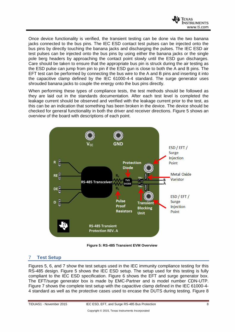
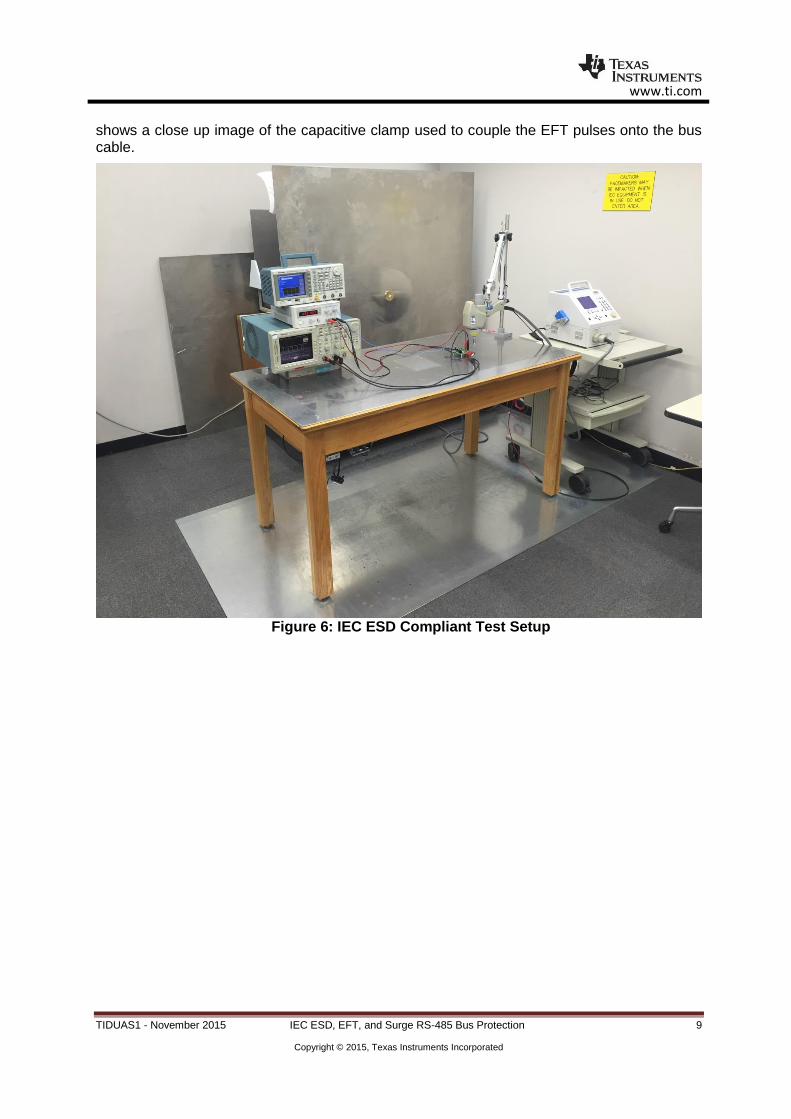
Test Setup 7
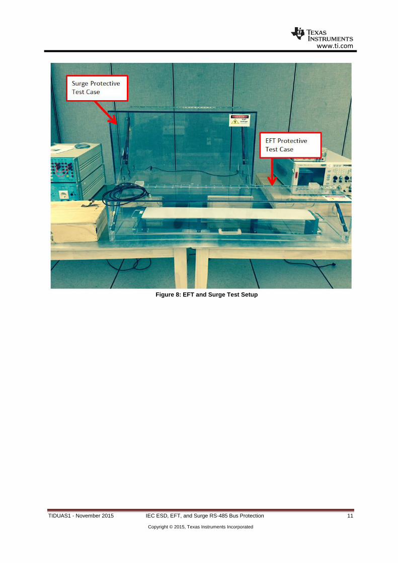
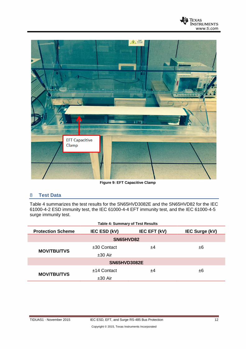
Figures 5, 6, and 7 show the test setups used in the IEC immunity compliance testing for this RS-485 design. Figure 5 shows the IEC ESD setup. The setup used for this testing is fully compliant to the IEC ESD specification. Figure 6 shows the EFT and surge generator box. The EFT/surge generator box is made by EMC-Partner and is model number CDN-UTP. Figure 7 shows the complete test setup with the capacitive clamp defined in the IEC 61000-4-4 standard as well as the protective cases used to encase the DUTS during testing. Figure 8
www.ti.com
TIDUAS1 - November 2015 IEC ESD, EFT, and Surge RS-485 Bus Protection 9
Copyright © 2015, Texas Instruments Incorporated
shows a close up image of the capacitive clamp used to couple the EFT pulses onto the bus cable.
Figure 6: IEC ESD Compliant Test Setup
www.ti.com
TIDUAS1 - November 2015 IEC ESD, EFT, and Surge RS-485 Bus Protection 10
Copyright © 2015, Texas Instruments Incorporated
Figure 7: Electrical Fast Transient (EFT) and Surge Generator
www.ti.com
TIDUAS1 - November 2015 IEC ESD, EFT, and Surge RS-485 Bus Protection 11
Copyright © 2015, Texas Instruments Incorporated
Figure 8: EFT and Surge Test Setup
www.ti.com
TIDUAS1 - November 2015 IEC ESD, EFT, and Surge RS-485 Bus Protection 12
Copyright © 2015, Texas Instruments Incorporated
Figure 9: EFT Capacitive Clamp
Test Data 8
Table 4 summarizes the test results for the SN65HVD3082E and the SN65HVD82 for the IEC 61000-4-2 ESD immunity test, the IEC 61000-4-4 EFT immunity test, and the IEC 61000-4-5 surge immunity test.
Table 4: Summary of Test Results
Protection Scheme IEC ESD (kV) IEC EFT (kV) IEC Surge (kV)
SN65HVD82
MOV/TBU/TVS ±30 Contact
±30 Air
±4 ±6
SN65HVD3082E
MOV/TBU/TVS ±14 Contact
±30 Air
±4 ±6

www.ti.com
TIDUAS1 - November 2015 IEC ESD, EFT, and Surge RS-485 Bus Protection 13
Copyright © 2015, Texas Instruments Incorporated
Table 5: IEC ESD Contact Discharge Test Results
Board 1 Board 2 Board 3 Board 1 Board 2 Board 3
+4kV
+5kV
+6kV
+7kV
+8kV
+9kV
+10kV
+11kV
+12kV
+13kV
+14kV
+15kV
+16kV NT NT NT
+17kV NT NT NT
+18kV NT NT NT
+19kV NT NT NT
+20kV NT NT NT
+21kV NT NT NT
+22kV NT NT NT
+23kV NT NT NT
+24kV NT NT NT
+25kV NT NT NT
+26kV NT NT NT
+27kV NT NT NT
+28kV NT NT NT
+29kV NT NT NT
+30kV NT NT NT
Board 1 Board 2 Board 3 Board 1 Board 2 Board 3
-4kV
-5kV
-6kV
-7kV
-8kV
-9kV
-10kV
-11kV
-12kV
-13kV
-14kV
-15kV
-16kV
-17kV
-18kV
-19kV
-20kV
-21kV
-22kV
-23kV
-24kV
-25kV
-26kV
-27kV
-28kV
-29kV
-30kV
RS-485 IEC ESD Test Results
Positive Contact ESD Strikes
IEC ESD LevelSN65HVD82 SN65HVD3082
Negative Contact ESD StrikesIEC ESD Level
www.ti.com
TIDUAS1 - November 2015 IEC ESD, EFT, and Surge RS-485 Bus Protection 14
Copyright © 2015, Texas Instruments Incorporated
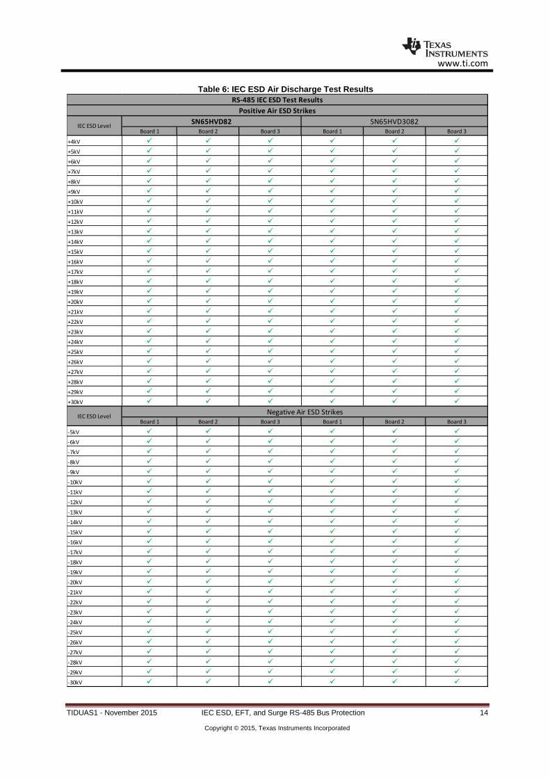
Table 6: IEC ESD Air Discharge Test Results
Board 1 Board 2 Board 3 Board 1 Board 2 Board 3
+4kV
+5kV
+6kV
+7kV
+8kV
+9kV
+10kV
+11kV
+12kV
+13kV
+14kV
+15kV
+16kV
+17kV
+18kV
+19kV
+20kV
+21kV
+22kV
+23kV
+24kV
+25kV
+26kV
+27kV
+28kV
+29kV
+30kV
Board 1 Board 2 Board 3 Board 1 Board 2 Board 3
-5kV
-6kV
-7kV
-8kV
-9kV
-10kV
-11kV
-12kV
-13kV
-14kV
-15kV
-16kV
-17kV
-18kV
-19kV
-20kV
-21kV
-22kV
-23kV
-24kV
-25kV
-26kV
-27kV
-28kV
-29kV
-30kV
RS-485 IEC ESD Test Results
Positive Air ESD Strikes
IEC ESD LevelSN65HVD82 SN65HVD3082
IEC ESD LevelNegative Air ESD Strikes
www.ti.com
TIDUAS1 - November 2015 IEC ESD, EFT, and Surge RS-485 Bus Protection 15
Copyright © 2015, Texas Instruments Incorporated
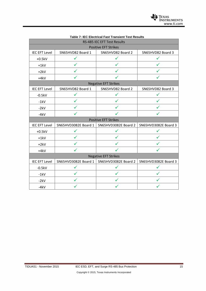
Table 7: IEC Electrical Fast Transient Test Results
RS-485 IEC EFT Test Results
Positive EFT Strikes
IEC EFT Level SN65HVD82 Board 1 SN65HVD82 Board 2 SN65HVD82 Board 3
+0.5kV
+1kV
+2kV
+4kV
Negative EFT Strikes
IEC EFT Level SN65HVD82 Board 1 SN65HVD82 Board 2 SN65HVD82 Board 3
-0.5kV
-1kV
-2kV
-4kV
Positive EFT Strikes
IEC EFT Level SN65HVD3082E Board 1 SN65HVD3082E Board 2 SN65HVD3082E Board 3
+0.5kV
+1kV
+2kV
+4kV
Negative EFT Strikes
IEC EFT Level SN65HVD3082E Board 1 SN65HVD3082E Board 2 SN65HVD3082E Board 3
-0.5kV
-1kV
-2kV
-4kV
www.ti.com
TIDUAS1 - November 2015 IEC ESD, EFT, and Surge RS-485 Bus Protection 16
Copyright © 2015, Texas Instruments Incorporated
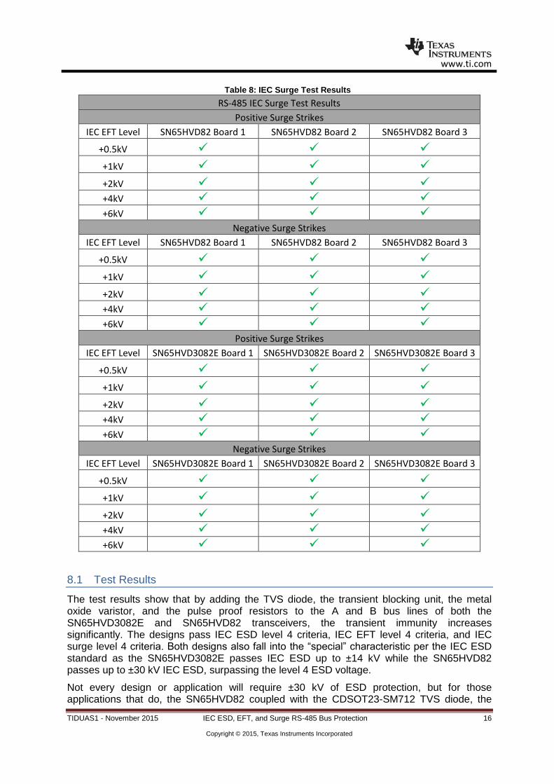
Table 8: IEC Surge Test Results
RS-485 IEC Surge Test Results
Positive Surge Strikes
IEC EFT Level SN65HVD82 Board 1 SN65HVD82 Board 2 SN65HVD82 Board 3
+0.5kV
+1kV
+2kV
+4kV
+6kV
Negative Surge Strikes
IEC EFT Level SN65HVD82 Board 1 SN65HVD82 Board 2 SN65HVD82 Board 3
+0.5kV
+1kV
+2kV
+4kV
+6kV
Positive Surge Strikes
IEC EFT Level SN65HVD3082E Board 1 SN65HVD3082E Board 2 SN65HVD3082E Board 3
+0.5kV
+1kV
+2kV
+4kV
+6kV
Negative Surge Strikes
IEC EFT Level SN65HVD3082E Board 1 SN65HVD3082E Board 2 SN65HVD3082E Board 3
+0.5kV
+1kV
+2kV
+4kV
+6kV
Test Results 8.1
The test results show that by adding the TVS diode, the transient blocking unit, the metal oxide varistor, and the pulse proof resistors to the A and B bus lines of both the SN65HVD3082E and SN65HVD82 transceivers, the transient immunity increases significantly. The designs pass IEC ESD level 4 criteria, IEC EFT level 4 criteria, and IEC surge level 4 criteria. Both designs also fall into the “special” characteristic per the IEC ESD standard as the SN65HVD3082E passes IEC ESD up to ±14 kV while the SN65HVD82 passes up to ±30 kV IEC ESD, surpassing the level 4 ESD voltage.
Not every design or application will require ±30 kV of ESD protection, but for those applications that do, the SN65HVD82 coupled with the CDSOT23-SM712 TVS diode, the
www.ti.com
TIDUAS1 - November 2015 IEC ESD, EFT, and Surge RS-485 Bus Protection 17
Copyright © 2015, Texas Instruments Incorporated
TBU-CA0065-200-WH, and the MOV-14D561KTR from Bourns will provide this as well as level 4 IEC ESD and surge protection.
For designs that do not require this level of protection but need to be rated up to level 4 IEC ESD (±8 kV), coupling the SN65HVD3082E with the same CDSOT23-SM712 TVS diode, TBU-CA0065-200-WH, and MOV-14D561KTR from Bourns takes a standard RS-485 transceiver with no integrated IEC ESD protection to ±14 kV IEC ESD protection and level 4 IEC EFT/surge.
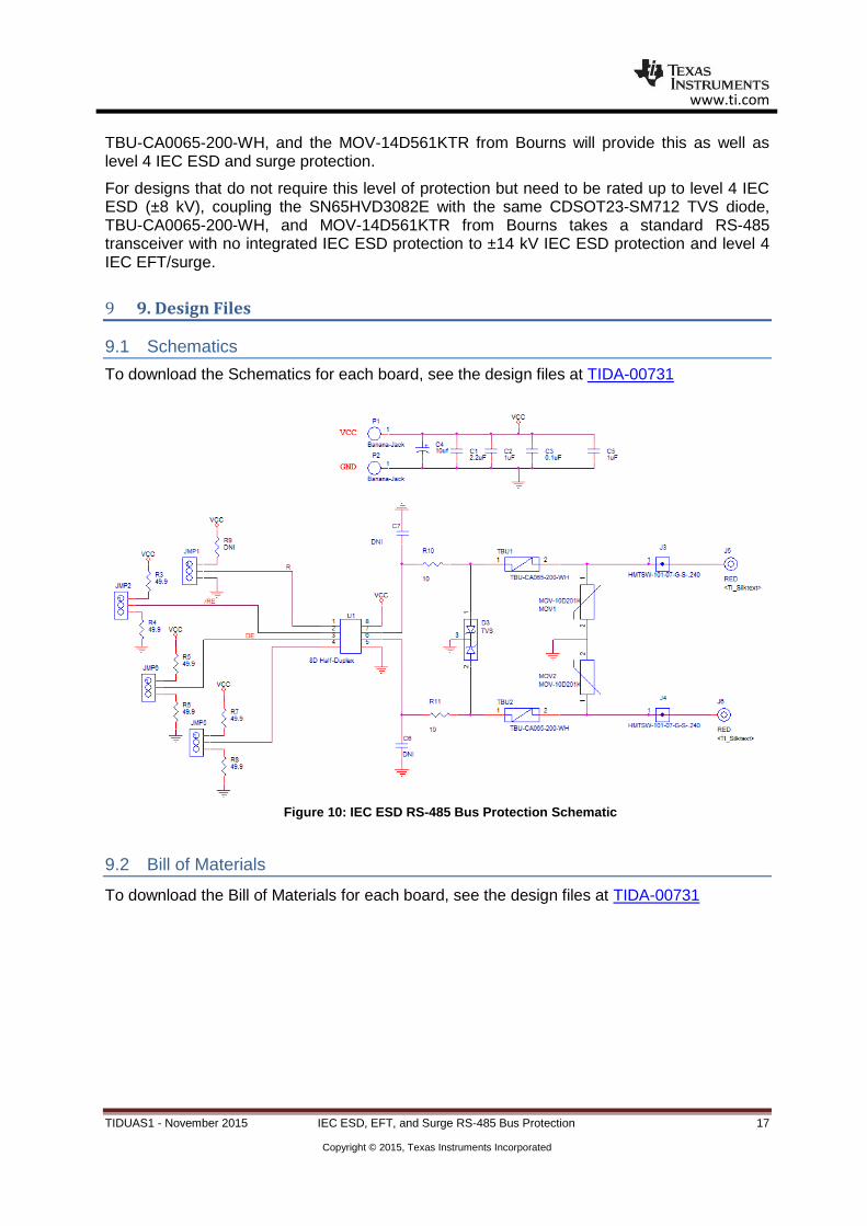
9. Design Files 9
Schematics 9.1
To download the Schematics for each board, see the design files at TIDA-00731
Figure 10: IEC ESD RS-485 Bus Protection Schematic
Bill of Materials 9.2
To download the Bill of Materials for each board, see the design files at TIDA-00731

www.ti.com
Table 1: TIDA-00731 BOM
Bill Of Materials TIDA-00731 – IEC ESD/EFT/Surge Protected RS-485
Item Qty Reference Value Manufacturer Manufacturer Part Number PCB Footprint
1 1 C1 10µF Any (5V+ Rating) T491D106K025AT 7343-31 (EIA)
2 1 C2 2.2µF Any (5V+ Rating) GRM31CR71H225KA88L 1206'
3 1 C3 1.0µF Any (5V+ Rating) C0805C105J4RACTU 0805'
4 2 C4, C5 0.1µF Any (5V+ Rating) GRM188R71H104KA93D 0603'
5 2 C6, C7 DNI Any (5V+ Rating) DNI DNI
6 1 D1 CDSOT23-SM712 Bourns Inc CDSOT23-SM712 SOT-23-3
7 2 J1, J2 Banana Plug - Metal Emerson Network Power 108-0740-001 4mm
8 12 JMP1, JMP2, JMP3, JMP4 HTSW-150-07-G-S Samtec Inc HTSW-150-07-G-S 0.1"
9 2 JMP5, JMP6 HTSW-150-07-G-S Samtec Inc HTSW-150-07-G-S 0.1"
10 2 MOV1, MOV2 MOV-14D561KTR Bourns Inc MOV-10D201K Disc 10mm
11 2 P1, P2 Banana Plug - Metal Emerson Network Power 108-0740-001 4mm
12 7 R1, R2, R3, R4, R5, R6, R7 49.9' Any (1% Tolerance) ERJ-3EKF49R9V 0603'
13 2 R8, R9 10.0 ohm Any (1% Tolerance) CRCW060310R0FKEAHP 0603'
14 2 TBU1, TBU2 TBU-CA065-200-WH Bourns TBU-CA065-200-WH SMD
15 1 U1 SN65HVD82 Texas Instruments SN65HVD82 SOIC
www.ti.com
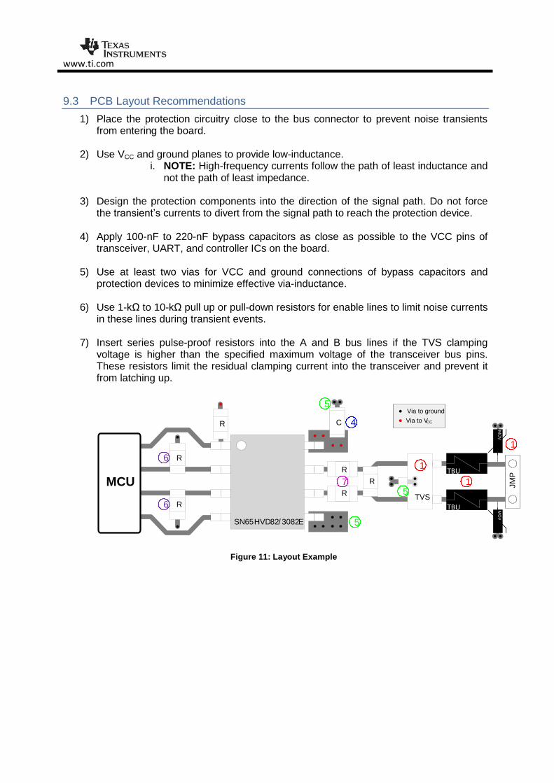
PCB Layout Recommendations 9.3
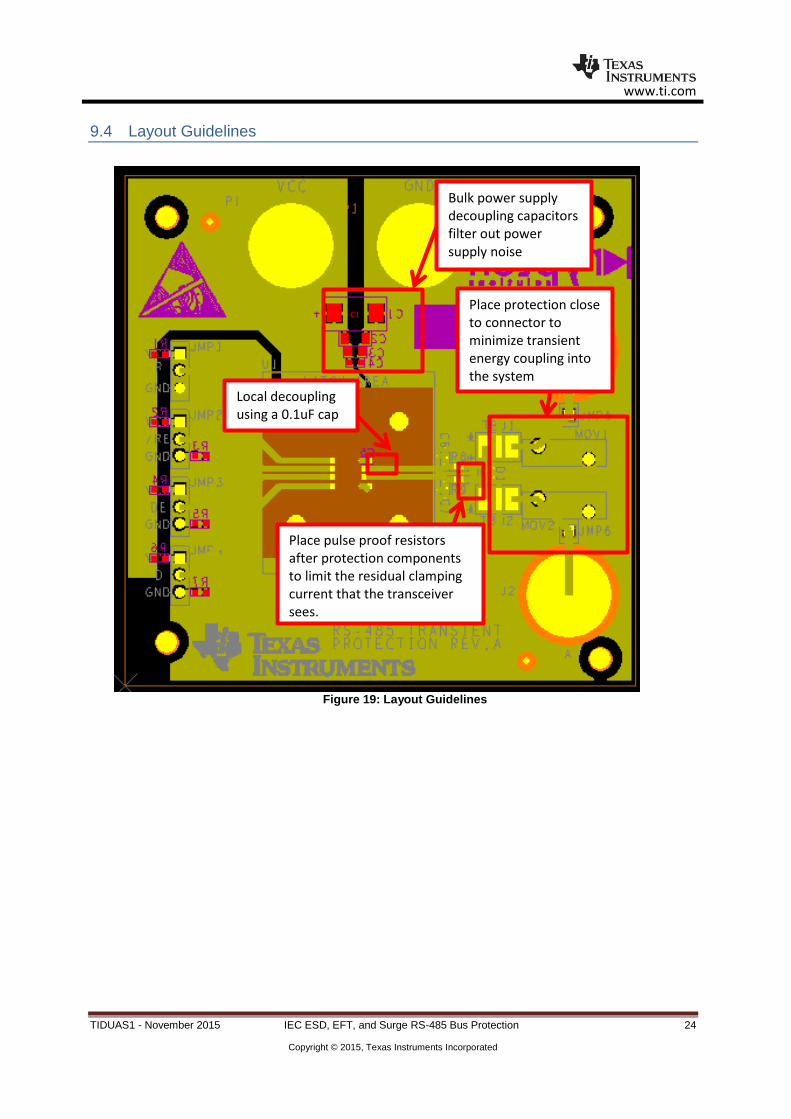
1) Place the protection circuitry close to the bus connector to prevent noise transients from entering the board.
2) Use VCC and ground planes to provide low-inductance. i. NOTE: High-frequency currents follow the path of least inductance and
not the path of least impedance.
3) Design the protection components into the direction of the signal path. Do not force the transient’s currents to divert from the signal path to reach the protection device.
4) Apply 100-nF to 220-nF bypass capacitors as close as possible to the VCC pins of transceiver, UART, and controller ICs on the board.
5) Use at least two vias for VCC and ground connections of bypass capacitors and
protection devices to minimize effective via-inductance.
6) Use 1-kΩ to 10-kΩ pull up or pull-down resistors for enable lines to limit noise currents in these lines during transient events.
7) Insert series pulse-proof resistors into the A and B bus lines if the TVS clamping
voltage is higher than the specified maximum voltage of the transceiver bus pins. These resistors limit the residual clamping current into the transceiver and prevent it from latching up.
MCUR
R
Via to ground
SN65HVD82/ 3082E
JM
P
R
R
R
C
5
6
6
1
4R
5
Via to VCC
TVS
75
TBU
TBU MO
VM
OV
1
1
Figure 11: Layout Example
www.ti.com
TIDUAS1 - November 2015 IEC ESD, EFT, and Surge RS-485 Bus Protection 20
Copyright © 2015, Texas Instruments Incorporated
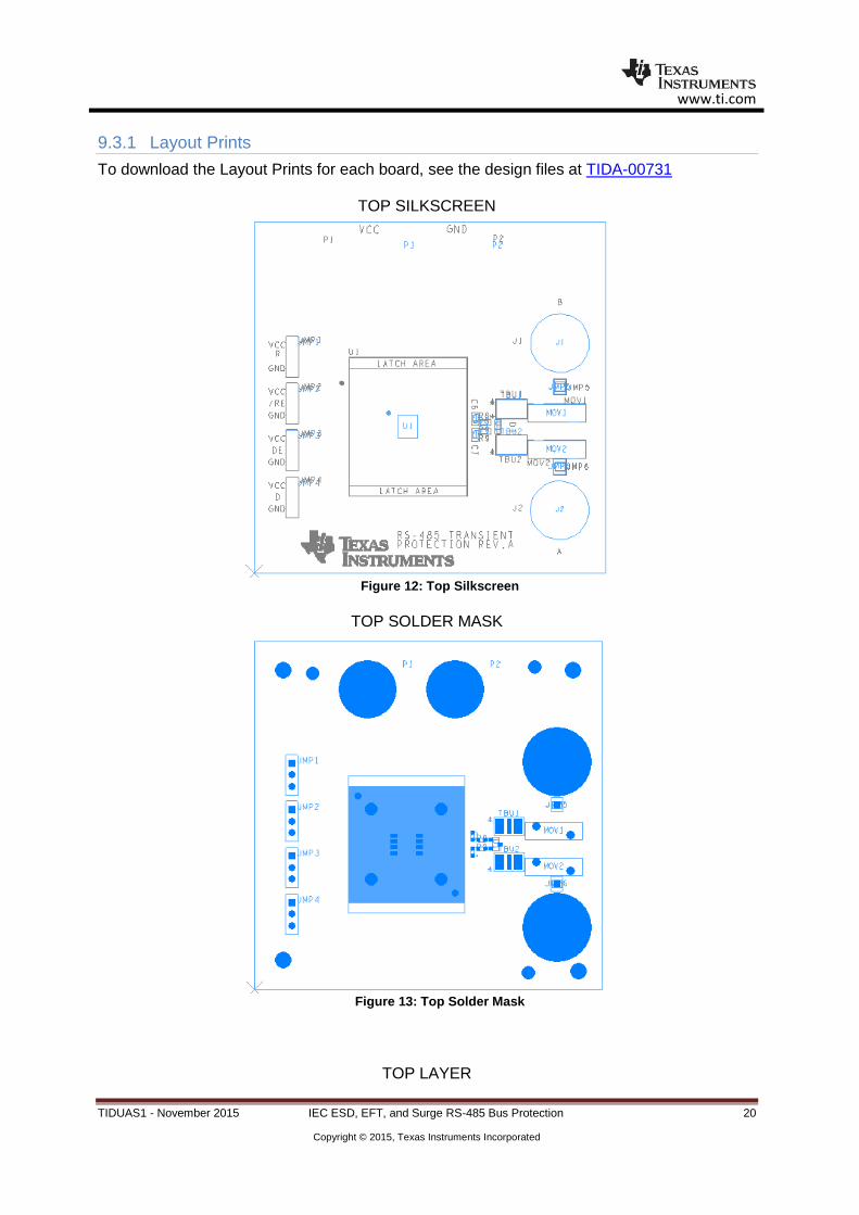
9.3.1 Layout Prints
To download the Layout Prints for each board, see the design files at TIDA-00731
TOP SILKSCREEN
Figure 12: Top Silkscreen
TOP SOLDER MASK
Figure 13: Top Solder Mask
TOP LAYER
www.ti.com
TIDUAS1 - November 2015 IEC ESD, EFT, and Surge RS-485 Bus Protection 21
Copyright © 2015, Texas Instruments Incorporated
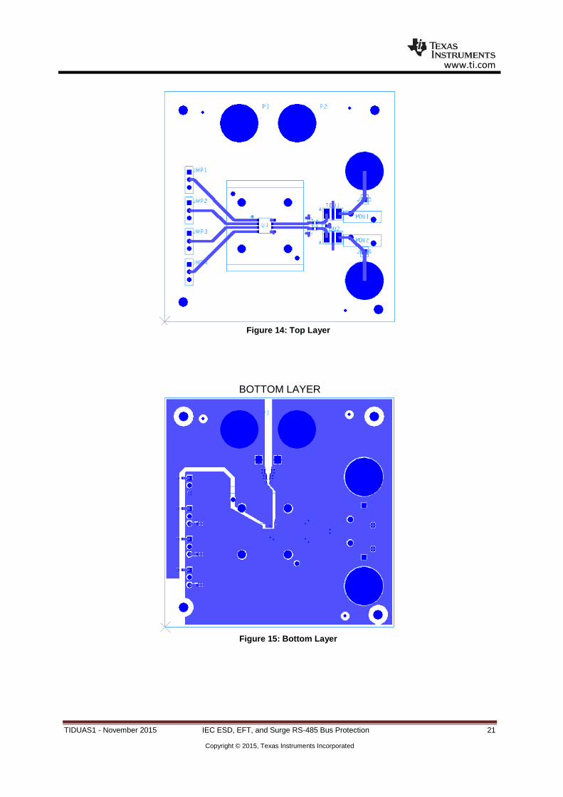
Figure 14: Top Layer
BOTTOM LAYER
Figure 15: Bottom Layer
www.ti.com
TIDUAS1 - November 2015 IEC ESD, EFT, and Surge RS-485 Bus Protection 22
Copyright © 2015, Texas Instruments Incorporated
BOTTOM SOLDER MASK
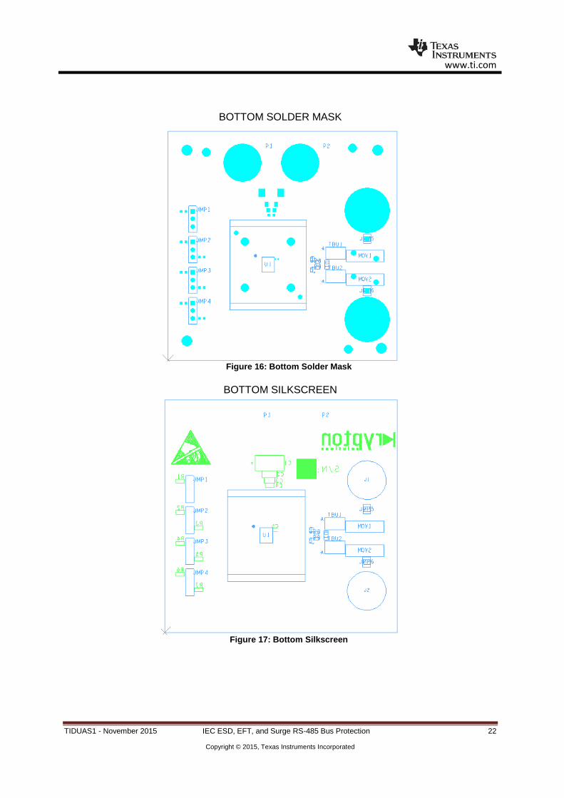
Figure 16: Bottom Solder Mask
BOTTOM SILKSCREEN
Figure 17: Bottom Silkscreen
www.ti.com
TIDUAS1 - November 2015 IEC ESD, EFT, and Surge RS-485 Bus Protection 23
Copyright © 2015, Texas Instruments Incorporated
MECHANICAL DIMENSIONS
Figure 18: Mechanical Dimensions
www.ti.com
TIDUAS1 - November 2015 IEC ESD, EFT, and Surge RS-485 Bus Protection 24
Copyright © 2015, Texas Instruments Incorporated
Layout Guidelines 9.4
Figure 19: Layout Guidelines
Bulk power supply decoupling capacitors filter out power supply noise
Local decoupling using a 0.1uF cap
Place protection close to connector to minimize transient energy coupling into the system
Place pulse proof resistors after protection components to limit the residual clamping current that the transceiver sees.

www.ti.com
Gerber files 9.5
To download the Gerber files for each board, see the design files at TIDA-00731
Figure 20: Gerber File
www.ti.com
TIDUAS1 - November 2015 IEC ESD, EFT, and Surge RS-485 Bus Protection 26
Copyright © 2015, Texas Instruments Incorporated
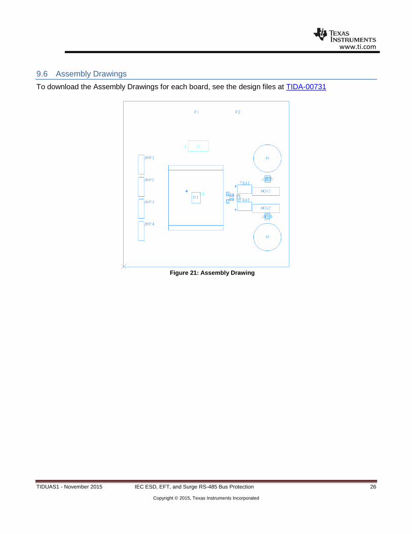
Assembly Drawings 9.6
To download the Assembly Drawings for each board, see the design files at TIDA-00731
Figure 21: Assembly Drawing
www.ti.com
TIDUAS1 - November 2015 IEC ESD, EFT, and Surge RS-485 Bus Protection 27
Copyright © 2015, Texas Instruments Incorporated
References 10
1. Texas Instruments Application Report, Protecting RS-485 Interfaces Against Lethal Electrical Transients, SLLA292A, 2009
About the Author 11
Michael Peffers is an applications engineer at Texas Instruments supporting the RS-485, LVDS, PECL, CAN, LIN, IO-Link, and Profibus interface products. Michael is responsible for developing reference designs solutions for the industrial segment and direct customer support including onsite support as well as onsite training. Michael is also responsible for producing technical content such as application notes, datasheets, white papers, and is the author of a recurring blog on the Texas Instruments E2E forum called Analog Wire: Get Connected. Michael brings to this role his experience in high-speed SERDES applications as well as experience in the optical transceiver space. Michael earned his Bachelors of Science in Electrical Engineering (BSEE) from the University of Central Florida (UCF).

IMPORTANT NOTICE FOR TI REFERENCE DESIGNS
Texas Instruments Incorporated ("TI") reference designs are solely intended to assist designers (“Buyers”) who are developing systems thatincorporate TI semiconductor products (also referred to herein as “components”). Buyer understands and agrees that Buyer remainsresponsible for using its independent analysis, evaluation and judgment in designing Buyer’s systems and products.TI reference designs have been created using standard laboratory conditions and engineering practices. TI has not conducted anytesting other than that specifically described in the published documentation for a particular reference design. TI may makecorrections, enhancements, improvements and other changes to its reference designs.Buyers are authorized to use TI reference designs with the TI component(s) identified in each particular reference design and to modify thereference design in the development of their end products. HOWEVER, NO OTHER LICENSE, EXPRESS OR IMPLIED, BY ESTOPPELOR OTHERWISE TO ANY OTHER TI INTELLECTUAL PROPERTY RIGHT, AND NO LICENSE TO ANY THIRD PARTY TECHNOLOGYOR INTELLECTUAL PROPERTY RIGHT, IS GRANTED HEREIN, including but not limited to any patent right, copyright, mask work right,or other intellectual property right relating to any combination, machine, or process in which TI components or services are used.Information published by TI regarding third-party products or services does not constitute a license to use such products or services, or awarranty or endorsement thereof. Use of such information may require a license from a third party under the patents or other intellectualproperty of the third party, or a license from TI under the patents or other intellectual property of TI.TI REFERENCE DESIGNS ARE PROVIDED "AS IS". TI MAKES NO WARRANTIES OR REPRESENTATIONS WITH REGARD TO THEREFERENCE DESIGNS OR USE OF THE REFERENCE DESIGNS, EXPRESS, IMPLIED OR STATUTORY, INCLUDING ACCURACY ORCOMPLETENESS. TI DISCLAIMS ANY WARRANTY OF TITLE AND ANY IMPLIED WARRANTIES OF MERCHANTABILITY, FITNESSFOR A PARTICULAR PURPOSE, QUIET ENJOYMENT, QUIET POSSESSION, AND NON-INFRINGEMENT OF ANY THIRD PARTYINTELLECTUAL PROPERTY RIGHTS WITH REGARD TO TI REFERENCE DESIGNS OR USE THEREOF. TI SHALL NOT BE LIABLEFOR AND SHALL NOT DEFEND OR INDEMNIFY BUYERS AGAINST ANY THIRD PARTY INFRINGEMENT CLAIM THAT RELATES TOOR IS BASED ON A COMBINATION OF COMPONENTS PROVIDED IN A TI REFERENCE DESIGN. IN NO EVENT SHALL TI BELIABLE FOR ANY ACTUAL, SPECIAL, INCIDENTAL, CONSEQUENTIAL OR INDIRECT DAMAGES, HOWEVER CAUSED, ON ANYTHEORY OF LIABILITY AND WHETHER OR NOT TI HAS BEEN ADVISED OF THE POSSIBILITY OF SUCH DAMAGES, ARISING INANY WAY OUT OF TI REFERENCE DESIGNS OR BUYER’S USE OF TI REFERENCE DESIGNS.TI reserves the right to make corrections, enhancements, improvements and other changes to its semiconductor products and services perJESD46, latest issue, and to discontinue any product or service per JESD48, latest issue. Buyers should obtain the latest relevantinformation before placing orders and should verify that such information is current and complete. All semiconductor products are soldsubject to TI’s terms and conditions of sale supplied at the time of order acknowledgment.TI warrants performance of its components to the specifications applicable at the time of sale, in accordance with the warranty in TI’s termsand conditions of sale of semiconductor products. Testing and other quality control techniques for TI components are used to the extent TIdeems necessary to support this warranty. Except where mandated by applicable law, testing of all parameters of each component is notnecessarily performed.TI assumes no liability for applications assistance or the design of Buyers’ products. Buyers are responsible for their products andapplications using TI components. To minimize the risks associated with Buyers’ products and applications, Buyers should provideadequate design and operating safeguards.Reproduction of significant portions of TI information in TI data books, data sheets or reference designs is permissible only if reproduction iswithout alteration and is accompanied by all associated warranties, conditions, limitations, and notices. TI is not responsible or liable forsuch altered documentation. Information of third parties may be subject to additional restrictions.Buyer acknowledges and agrees that it is solely responsible for compliance with all legal, regulatory and safety-related requirementsconcerning its products, and any use of TI components in its applications, notwithstanding any applications-related information or supportthat may be provided by TI. Buyer represents and agrees that it has all the necessary expertise to create and implement safeguards thatanticipate dangerous failures, monitor failures and their consequences, lessen the likelihood of dangerous failures and take appropriateremedial actions. Buyer will fully indemnify TI and its representatives against any damages arising out of the use of any TI components inBuyer’s safety-critical applications.In some cases, TI components may be promoted specifically to facilitate safety-related applications. With such components, TI’s goal is tohelp enable customers to design and create their own end-product solutions that meet applicable functional safety standards andrequirements. Nonetheless, such components are subject to these terms.No TI components are authorized for use in FDA Class III (or similar life-critical medical equipment) unless authorized officers of the partieshave executed an agreement specifically governing such use.Only those TI components that TI has specifically designated as military grade or “enhanced plastic” are designed and intended for use inmilitary/aerospace applications or environments. Buyer acknowledges and agrees that any military or aerospace use of TI components thathave not been so designated is solely at Buyer's risk, and Buyer is solely responsible for compliance with all legal and regulatoryrequirements in connection with such use.TI has specifically designated certain components as meeting ISO/TS16949 requirements, mainly for automotive use. In any case of use ofnon-designated products, TI will not be responsible for any failure to meet ISO/TS16949.IMPORTANT NOTICE
Mailing Address: Texas Instruments, Post Office Box 655303, Dallas, Texas 75265Copyright © 2015, Texas Instruments Incorporated