Embed Size (px)
Citation preview
8/15/2019 TI Selection Guide
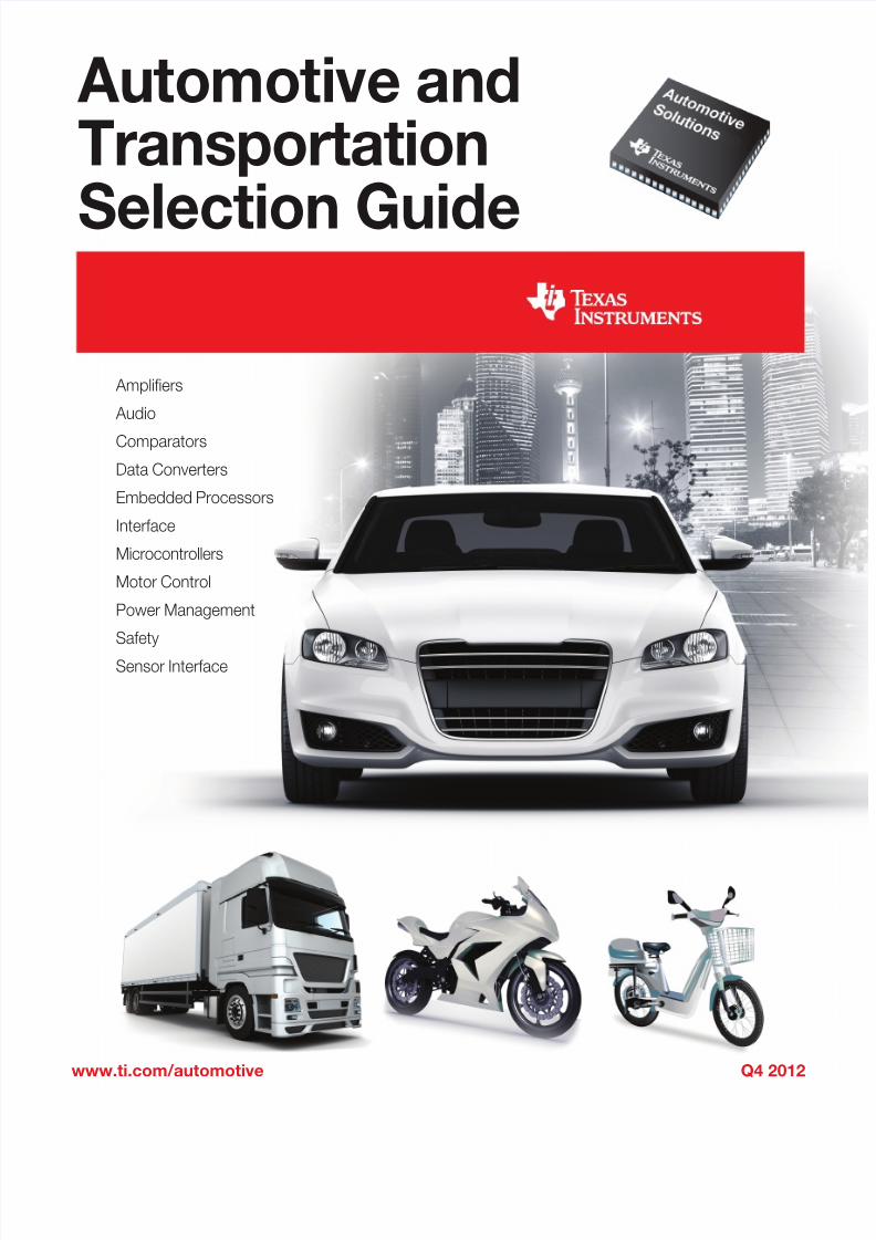
http://slidepdf.com/reader/full/ti-selection-guide 1/49Q4 2012www.ti.com/automotive
Automotive andTransportation
Selection Guide
Amplifiers
Audio
Comparators
Data Converters
Embedded Processors
Interface
Microcontrollers
Motor Control
Power Management
SafetySensor Interface
8/15/2019 TI Selection Guide
http://slidepdf.com/reader/full/ti-selection-guide 2/49
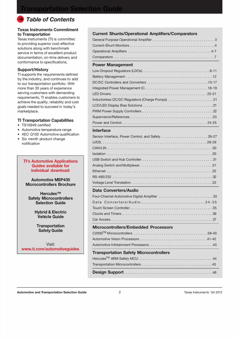
2 Automotive and Transportation Selection Guide Texas Instruments Q4 2012
➔
Transportation Selection Guide
Table of Contents
Current Shunts/Operational Amplifiers/ComparatorsGeneral Purpose Operational Amplifier . . . . . . . . . . . . . . . . . . . . . . . . . . . . . . . . . 3
Current-Shunt Monitors . . . . . . . . . . . . . . . . . . . . . . . . . . . . . . . . . . . . . . . . . . . . .4
Operational Amplifiers . . . . . . . . . . . . . . . . . . . . . . . . . . . . . . . . . . . . . . . . . . . . 4-7
Comparators . . . . . . . . . . . . . . . . . . . . . . . . . . . . . . . . . . . . . . . . . . . . . . . . . . . . . 7Power ManagementLow-Dropout Regulators (LDOs) . . . . . . . . . . . . . . . . . . . . . . . . . . . . . . . . . . . 8-11
Battery Management . . . . . . . . . . . . . . . . . . . . . . . . . . . . . . . . . . . . . . . . . . . . . .12
DC/DC Controllers and Converters . . . . . . . . . . . . . . . . . . . . . . . . . . . . . . . . 13-17
Integrated Power Management IC . . . . . . . . . . . . . . . . . . . . . . . . . . . . . . . . . 18-19
LED Drivers. . . . . . . . . . . . . . . . . . . . . . . . . . . . . . . . . . . . . . . . . . . . . . . . . . . 20-21
Inductorless DC/DC Regulators (Charge Pumps) . . . . . . . . . . . . . . . . . . . . . . . .21
LCD/LED Display Bias Solutions . . . . . . . . . . . . . . . . . . . . . . . . . . . . . . . . . . . . . 21
PWM Power Supply Controllers . . . . . . . . . . . . . . . . . . . . . . . . . . . . . . . . . . . . . . 22
Supervisors/References . . . . . . . . . . . . . . . . . . . . . . . . . . . . . . . . . . . . . . . . . . . .23Power and Control . . . . . . . . . . . . . . . . . . . . . . . . . . . . . . . . . . . . . . . . . . . . . 24-25
InterfaceSensor Interface, Power Control, and Safety. . . . . . . . . . . . . . . . . . . . . . . . . 26-27
LVDS. . . . . . . . . . . . . . . . . . . . . . . . . . . . . . . . . . . . . . . . . . . . . . . . . . . . . . . . 28-29
CAN/LIN . . . . . . . . . . . . . . . . . . . . . . . . . . . . . . . . . . . . . . . . . . . . . . . . . . . . . . . . 30
Isolation . . . . . . . . . . . . . . . . . . . . . . . . . . . . . . . . . . . . . . . . . . . . . . . . . . . . . . . .30
USB Switch and Hub Controller. . . . . . . . . . . . . . . . . . . . . . . . . . . . . . . . . . . . . . 31
Analog Switch and Multiplexer. . . . . . . . . . . . . . . . . . . . . . . . . . . . . . . . . . . . . . .31
Ethernet . . . . . . . . . . . . . . . . . . . . . . . . . . . . . . . . . . . . . . . . . . . . . . . . . . . . . . . .32
RS-485/232 . . . . . . . . . . . . . . . . . . . . . . . . . . . . . . . . . . . . . . . . . . . . . . . . . . . . . 32 Voltage Level Translation . . . . . . . . . . . . . . . . . . . . . . . . . . . . . . . . . . . . . . . . . . .32
Data Converters/AudioFour-Channel Automotive Digital Amplifier . . . . . . . . . . . . . . . . . . . . . . . . . . . . .33
D a t a C o n v e r t e r s / A u d i o . . . . . . . . . . . . . . . . . . . . . . . . . . . . . . . . . . . . . . . . . . 3 4 - 3 5
Touch Screen Controller . . . . . . . . . . . . . . . . . . . . . . . . . . . . . . . . . . . . . . . . . . . .35
Clocks and Timers . . . . . . . . . . . . . . . . . . . . . . . . . . . . . . . . . . . . . . . . . . . . . . . . 36
Car Access . . . . . . . . . . . . . . . . . . . . . . . . . . . . . . . . . . . . . . . . . . . . . . . . . . . . . . 37
Microcontrollers/Embedded Processors
C2000TM
Microcontrollers . . . . . . . . . . . . . . . . . . . . . . . . . . . . . . . . . . . . . . . 38-40 Automotive Vision Processors . . . . . . . . . . . . . . . . . . . . . . . . . . . . . . . . . . . . 41-42
Automotive Infotainment Processors . . . . . . . . . . . . . . . . . . . . . . . . . . . . . . . . . .43
Transportation Safety MicrocontrollersHercules TM ARM Safety MCU . . . . . . . . . . . . . . . . . . . . . . . . . . . . . . . . . . . . . . .44
Transportation Microcontrollers . . . . . . . . . . . . . . . . . . . . . . . . . . . . . . . . . . . . . . 45
Design Support . . . . . . . . . . . . . . . . . . . . . . . . . . . . . . . . . . . . . . . . . . . . . . . 46
Texas Instruments Commitmentto TransportationTexas Instruments (TI) is committedto providing superior cost-effectivesolutions along with benchmarkservice in terms of excellent product
documentation, on-time delivery andconformance to specifications.
Support/History TI supports the requirements definedby the industry, and continues to addto our transportation portfolio. Withmore than 30 years of experienceserving customers with demandingrequirements, TI enables customers toachieve the quality, reliability and costgoals needed to succeed in today’smarketplace.
TI Transportation Capabilities• TS16949 certified• Automotive temperature range• AEC Q100 Automotive qualification• Six month product change
notification
TI’s Automotive ApplicationsGuides available forindividual download:
Automotive MSP430Microcontrollers Brochure
Hercules™Safety Microcontrollers
Selection Guide
Hybrid & Electric Vehicle Guide
TransportationSafety Guide
Visit:www.ti.com/automotiveguides
8/15/2019 TI Selection Guide
http://slidepdf.com/reader/full/ti-selection-guide 3/49
3 Automotive and Transportation Selection Guide Texas Instruments Q4 2012
➔
Current Shunts/Operational Amplifiers/Comparators
General Purpose Operational Amplifier
High voltage (36 V), Low Power, Rail-Rail Operational AmplifierOPA171-Q1
Get samples and datasheets at: www.ti.com/sc/device/ opa171-q1
Key Features
• Dynamic input voltage range of +2.7 V to +36 V or ±1.35 V to ±18 V allowsfor greater design versatility acrossvarying supply rails, while stillenabling precise, low-voltage sensoroutputs.
• The OPA171-Q1 provides precisionperformance, including low offset ofup to 1.8 mV, typical drift of 0.3 uV/Cand wide gain bandwidth of 3 Mhz.
• Low quiescent current of 475 uAenables efficient battery-poweredoperation.
Applications• Automotive HEV/EV• Automotive Body applications• Tracking Amplifier in Power Modules• Transducer Amplifiers
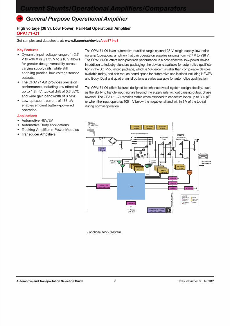
The OPA171-Q1 is an automotive-qualified single channel 36-V, single-supply, low-noise
op amp (operational amplifier) that can operate on supplies ranging from +2.7 V to +36 V.The OPA171-Q1 offers high-precision performance in a cost-effective, low-power device.In addition to industry-standard packaging, the device is available for automotive qualifica-tion in the SOT-553 micro package, which is 50-percent smaller than comparable devicesavailable today, and can reduce board space for automotive applications including HEV/EVand Body. Dual and quad channel options are also available for automotive qualification.
The OPA171-Q1 offers features designed to enhance overall system design stability, suchas the ability to handle input signals beyond the supply rails without causing output phasereversal. The OPA171-Q1 remains stable when exposed to capacitive loads up to 300 pFor when the input operates 100 mV below the negative rail and within 2 V of the top railduring normal operation.
AC Line8S – 265V AC
RelayDrivers
Power LineCommunications
VoltageSense
CurrentSense
CurrentSense
SystemPower
Core and I/OPower
AuxiliaryPower
MOSFETDrivers
MCU
Interface
To VehicleCAN Bus
4-Phase Interleaved PFC
Full-bridgeDriver
Boosted DCOutput 400+ V DC
High-voltageBattery pack
MOSFETDrivers
MOSFET
Drivers
Isolation
Temperature Sensor and Fan Control
I s o
l a t i o n
B o u n
d a r y
Isolation
Isolation Interface
ADC
LEGEND Processor Interface RF/IF Amplifier Logic
Power ADC/DACClocksOther
Functional block diagram.
8/15/2019 TI Selection Guide
http://slidepdf.com/reader/full/ti-selection-guide 4/49
➔
4 Automotive and Transportation Selection Guide Texas Instruments Q4 2012
Current Shunts/Operational Amplifiers/Comparators
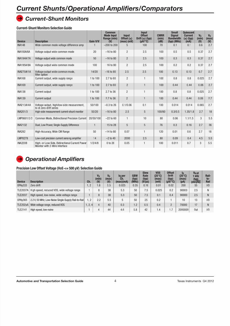
Current-Shunt Monitors
Current-Shunt Monitors Selection Guide
Device Description Gain V/V
CommonMode Input
Range (min)(V)
InputOffset (±)
(max) (mV)
InputOffset
Drift (±) (typ)(µV/°C)
CMRR(min)(dB)
SmallSignal
Bandwidth(typ) (MHz)
QuiescentCurrent(±) (typ)
(mA)
VS(min)
(V)
VS(max)
(V)INA148 Wide common mode voltage difference amp 1 –200 to 200 5 100 70 0.1 0.1 0.6 2.7
INA193A/6A Voltage output wide common mode 20 –16 to 80 2 2.5 100 0.5 0.5 0.37 2.7
INA194A/7A Voltage output wide common mode 50 –16 to 80 2 2.5 100 0.3 0.3 0.37 2.7
INA195A/8A Voltage output wide common mode 100 –16 to 80 2 2.5 100 0.2 0.2 0.37 2.7
INA270A/1A Voltage output wide common mode,lter option
14/20 –16 to 80 2.5 2.5 100 0.13 0.13 0.7 2.7
INA168 Current output, wide supply range 1 to 100 2.7 to 60 2 1 100 0.8 0.8 0.025 2.7
INA169 Current output, wide supply range 1 to 100 2.7 to 60 2 1 100 0.44 0.44 0.06 2.7
INA138 Current output 1 to 100 2.7 to 36 2 1 100 0.8 0.8 0.025 2.7
INA139 Current output 1 to 100 2.7 to 36 2 1 100 0.44 0.44 0.06 2.7
INA213A/4A Voltage output, high/low-side measurement,bi-di zero-drift series
50/100 –0.3 to 26 0.1/0.06 0.1 100 0.014 0.014 0.065 2.7
INA201/3 High-side measurement current-shunt monitor 50/20 –16 to 80 2.5 5 100/80 0.3/0.5 1.35/1.8 2.7 18
LMP8601/2/3 Common Mode, Bidirectional Precision Current 20/50/100 –22 to 60 1 10 80 0.06 1.1/1.5 3 5.5
INA2132 Dual, Low Power, Single-Supply Difference 1 –15 to 28 5 5 76 0.3 0.16 2.7 36
INA282 High-Accuracy, Wide CM Range 50 –14 to 80 0.07 1 120 0.01 0.6 2.7 18
LMP8278 Low-cost precision current sensing amplier 14 –2 to 40 2000 2.5 80 0.09 0.4 4.5 5.5
INA220B High- or Low-Side, Bidirectional Current PowerMonitor with 2-Wire Interface
1/2/4/8 0 to 26 0.05 1 100 0.011 0.7 3 5.5
Precision Low Offset Voltage (VoS <= 500 μV) Selection Guide
Device Description Ch.
VS(min)
(V)
VS(max)
(V)
Iq perCh.
(max)(mA)
GBW(typ)
(MHz)
SlewRate(typ)
(V/µs)
VOS(25°C)(max)(mV)
OffsetDrift(typ)
(µV/°C)
IB (25°C)(max)(pA)
VNat1 kHz(typ)
(nV/ Hz)
Rail-to-Rail
OPAy333 Zero drift 1, 2 1.8 5.5 0.025 0.35 0.16 0.01 0.02 200 55 I/O
TLE2037A High speed, reduced VOS, wide voltage range 1 8 38 5.3 50 7.5 0.025 0.2 90000 2.5 N
TLE2037 High speed, low-noise, wide voltage range 1 8 38 5.3 50 7.5 0.1 0.4 90000 2.5 N
OPAy365 2.2 V, 50 MHz, Low-Noise Single-Supply Rail-to-Rail 1, 2 2.2 5.5 5 50 25 0.2 1 10 13 I/O
TLE202xA Wide voltage range, reduced VOS 1, 2, 4 4 40 0.3 1.2 0.5 0.4 2 70000 17 N
TLE2141 High speed, low-noise 1 4 44 4.6 5.8 42 1.4 1.7 2000000 Out I/O
➔ Operational Amplifiers
8/15/2019 TI Selection Guide
http://slidepdf.com/reader/full/ti-selection-guide 5/49
➔
5 Automotive and Transportation Selection Guide Texas Instruments Q4 2012
Current Shunts/Operational Amplifiers/Comparators
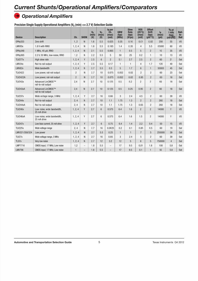
Operational Amplifiers
Precision Single Supply Operational Ampliers (VS (min) <= 2.7 V) Selection Guide
Device Description Ch. SHDN
VS(min)
(V)
VS(max)
(V)
Iq perCh.
(max)(mA)
GBW(typ)
(MHz)
SlewRate(typ)
(V/µs)
VOS (25°C)(max)(mV)
OffsetDrift(typ)
(µV/°C)
IB (max)(pA)
VN at1 kHz(typ)
(nV/ Hz)
Rail-to-Rail
OPAy333 Zero drift 1, 2 N 1.8 5.5 0.025 0.35 0.16 0.01 0.02 200 55 I/O
LMV93x 1.8 V with RRIO 1, 2, 4 N 1.8 5.5 0.185 1.4 0.35 4 5.5 65000 60 I/O
OPAy348 1 MHz, 45 µA, RRIO 1, 2, 4 N 2.1 5.5 0.065 1 0.5 5 2 10 35 I/O
OPAy365 2.2 V, 50 MHz, low-noise, RRIO 1,2 N 2.2 5.5 5 50 25 0.2 1 10 13 I/O
TLV277x High slew rate 1, 2, 4 Y 2.5 6 2 5.1 2.7 2.5 2 60 21 Out
LMV34x Rail-to-rail output 1, 2, 4 Y 2.5 5.5 0.17 1 1 4 1.7 120 40 Out
LMV82x Wide bandwidth 1, 2, 4 N 2.7 5.5 0.3 5 1.7 6 1 90000 45 Out
TLV2422 Low power, rail-rail output 2 N 2.7 10 0.075 0.052 0.02 2 2 60 23 Out
TLV2422A Low power, rail-rail output 2 N 2.7 10 0.075 0.052 0.02 0.95 2 60 18 Out
TLV243x Advanced LinCMOS™rail-to-rail output
2,4 N 2.7 10 0.125 0.5 0.2 2 2 60 18 Out
TLV243xA Advanced LinCMOS™rail-to-rail output
2,4 N 2.7 10 0.125 0.5 0.25 0.95 2 60 18 Out
TLV237x Wide voltage range, 3 MHz 1, 2, 4 Y 2.7 16 0.66 3 2.4 4.5 2 60 39 I/OTLV244x Rail-to-rail output 2, 4 N 2.7 10 1.1 1.75 1.3 2 2 260 18 Out
TLV244xA Rail-to-rail output 2, 4 N 2.7 10 1.1 1.75 1.3 0.65 2 260 18 Out
TLV246x Low noise, wide bandwidth,25 mA drive
1, 2, 4 Y 2.7 6 0.575 6.4 1.6 2 2 14000 11 I/O
TLV246xA Low noise, wide bandwidth,25 mA drive
1, 2, 4 Y 2.7 6 0.575 6.4 1.6 1.5 2 14000 11 I/O
TLV247x Low bias current, 35 mA drive 1, 2, 4 Y 2.7 6 0.75 6.4 1.4 2.2 0.4 50 15 I/O
TLV225x Wide voltage range 2, 4 N 2.7 16 0.0625 0.2 0.1 0.85 0.5 60 19 Out
LMV321/358/324 Low power 1, 2, 4 N 2.7 5.5 0.25 1 1 7 5 250000 39 Out
TLV27x Wide voltage range, 3 MHz 1, 2, 4 N 2.7 16 0.66 3 2.4 5 2 60 39 Out
TL97x Very low noise 1, 2, 4 N 2.7 12 3.2 12 5 6 5 750000 4 Out
LMP7716 CMOS input, 17 MHz, Low noise 1,2 – 1.8 5.5 – 17 9.5 0,01 1.8 100 5.8 OutLMV796 CMOS input, 17 MHz, Low noise 1 – 1.8 5.5 – 17 9.5 0.1 1 50 5.8 Out
8/15/2019 TI Selection Guide
http://slidepdf.com/reader/full/ti-selection-guide 6/49
➔
6 Automotive and Transportation Selection Guide Texas Instruments Q4 2012
Current Shunts/Operational Amplifiers/Comparators
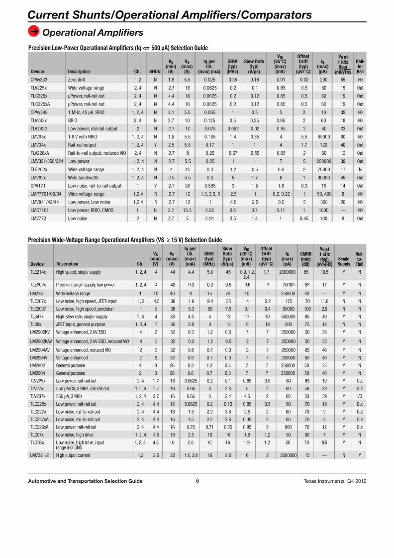
Operational AmplifiersPrecision Low-Power Operational Ampliers (Iq <= 500 µA) Selection Guide
Device Description Ch. SHDN
VS(min)
(V)
VS(max)
(V)
Iq perCh.
(max) (mA)
GBW(typ)
(MHz)
Slew Rate(typ)
(V/µs)
VIO(25°C)(max)(mV)
OffsetDrift(typ)
(µV/°C)
IB (max)(pA)
VNat1 kHz(typ)
(nV/ Hz)
Rail-to-Rail
OPAy333 Zero drift 1, 2 N 1.8 5.5 0.025 0.35 0.16 0.01 0.02 200 55 I/O
TLV225x Wide voltage range 2, 4 N 2.7 16 0.0625 0.2 0.1 0.85 0.5 60 19 Out
TLC225x µPower, rail-rail out 2, 4 N 4.4 16 0.0625 0.2 0.12 0.85 0.5 60 19 OutTLC225xA µPower, rail-rail out 2, 4 N 4.4 16 0.0625 0.2 0.12 0.85 0.5 60 19 Out
OPAy348 1 MHz, 45 µA, RRIO 1, 2, 4 N 2.1 5.5 0.065 1 0.5 5 2 10 35 I/O
TLV243x RRIO 2, 4 N 2.7 10 0.125 0.5 0.25 0.95 2 60 18 I/O
TLV2422 Low power, rail-rail output 2 N 2.7 10 0.075 0.052 0.02 0.95 2 60 23 Out
LMV93x 1.8 V with RRIO 1, 2, 4 N 1.8 5.5 0.185 1.4 0.35 4 5.5 65000 60 I/O
LMV34x Rail-rail output 1, 2, 4 Y 2.5 5.5 0.17 1 1 4 1.7 120 40 Out
TLV226xA Rail-to-rail output, reduced VIO 2, 4 N 2.7 8 0.25 0.67 0.55 0.95 2 60 12 Out
LMV321/358/324 Low power 1, 2, 4 N 2.7 5.5 0.25 1 1 7 5 250000 39 Out
TLE202x Wide voltage range 1, 2, 4 N 4 40 0.3 1.2 0.5 0.6 2 70000 17 N
LMV82x Wide bandwidth 1, 2, 4 N 2.5 5.5 0.3 5 1.7 6 1 90000 45 Out
OPA171 Low noise, rail-to-rail output 1 Y 2.7 36 0.595 3 1.5 1.8 0.3 15 14 Out
LMP7701/02/04 Wide voltage range 1,2,4 N 2.7 12 1.3, 2.5, 5 2.5 1 0.2, 0.22 1 50, 400 9 I/OLMV841/42/44 Low power, Low noise 1,2,4 N 2.7 12 1 4.5 2.5 0.5 5 300 20 I/O
LMC7101 Low power, RRIO, CMOS 1 N 2.7 15.5 0.95 0.6 0.7 0.11 1 1000 — I/O
LMV772 Low noise 2 N 2.7 5 0.91 3.5 1.4 1 0.45 100 9 Out
Precision Wide-Voltage Range Operational Ampliers (VS ≥ 15 V) Selection Guide
Device Description Ch.
VS(min)
(V)
VS(max)
(V)
Iq perCh.
(max)(mA)
GBW(typ)
(MHz)
SlewRate(typ)
(V/µs)
VIO (25°C)(max)(mV)
OffsetDrift(typ)
(µV/°C)
IB (max)(pA)
CMRR(min)(dB)
VNat1 kHz(typ)
(nV/ Hz)SingleSupply
Rail-to-Rail
TLE214x High speed, single supply 1, 2, 4 4 44 4.4 5.8 45 0.9, 1.2,2.4
1.7 2000000 85 10.5 Y N
TLE202x Precision, single supply, low power 1, 2, 4 4 40 0.3 0.3 0.5 0.6 2 70000 85 17 Y N
LM218 Wide voltage range 1 10 40 8 15 70 10 — 250000 80 — Y N
TLE207x Low noise, high speed, JFET-input 1, 2 4.5 38 1.8 9.4 35 4 3.2 175 70 11.6 N N
TLE2037 Low noise, high speed, precision 1 8 38 5.3 50 7.5 0.1 0.4 90000 100 2.5 N N
TL347x High-slew rate, single-supply 2, 4 4 36 4.5 4 13 17 10 500000 65 49 Y N
TL08x JFET input, general purpose 1, 2, 4 7 36 2.8 3 13 9 18 200 75 18 N N
LM2902KV Voltage enhanced, 2 kV ESD 4 3 32 0.3 1.2 0.5 7 7 250000 50 35 Y N
LM2902KAV Voltage enhanced, 2 kV ESD, reduced VIO 4 3 32 0.3 1.2 0.5 2 7 250000 50 35 Y N
LM2904AV Voltage enhanced, reduced VIO 2 3 32 0.6 0.7 0.3 2 7 250000 65 40 Y N
LM2904V Voltage enhanced 2 3 32 0.6 0.7 0.3 7 7 250000 65 40 Y N
LM2902 General purpose 4 3 26 0.3 1.2 0.5 7 7 250000 50 35 Y N
LM2904 General purpose 2 3 26 0.6 0.7 0.3 7 7 250000 50 40 Y N
TLV225x Low power, rail-rail out 2, 4 2.7 16 0.0625 0.2 0.1 0.85 0.5 60 65 19 Y Out
TLV27x 550 µA/Ch, 3 MHz, rail-rail out 1, 2, 4 2.7 16 0.66 3 2.4 5 2 60 58 39 Y Out
TLV237x 550 µA, 3 MHz 1, 2, 4 2.7 16 0.66 3 2.4 4.5 2 60 50 39 Y I/O
TLC225x Low power, rail-rail out 2, 4 4.4 16 0.0625 0.2 0.12 0.85 0.5 60 70 19 Y Out
TLC227x Low noise, rail-to-rail out 2, 4 4.4 16 1.5 2.2 3.6 2.5 2 60 70 9 Y Out
TLC227xA Low noise, rail-to-rail out 2, 4 4.4 16 1.5 2.2 3.6 0.95 2 60 70 9 Y Out
TLC226xA Low power, rail-rail out 2, 4 4.4 16 0.25 0.71 0.55 0.95 5 800 70 12 Y Out
TLC07x Low noise, high drive 1, 2, 4 4.5 16 2.5 10 16 1.9 1.2 50 80 7 Y N
TLC08x Low noise, high drive, inputrange incl GND
1, 2, 4 4.5 16 2.5 10 16 1.9 1.2 50 70 8.5 Y N
LM7321/2 High output current 1,2 2.5 32 1.9, 3.8 16 8.5 6 2 2500000 15 — N Y
8/15/2019 TI Selection Guide
http://slidepdf.com/reader/full/ti-selection-guide 7/49
➔
7 Automotive and Transportation Selection Guide Texas Instruments Q4 2012
Current Shunts/Operational Amplifiers/Comparators
Operational Amplifiers
➔
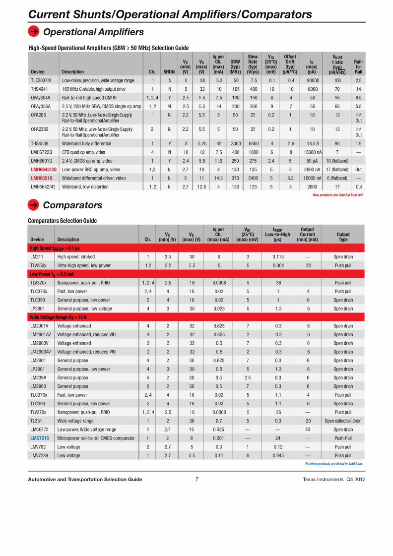
High-Speed Operational Ampliers (GBW ≥ 50 MHz) Selection Guide
Device Description Ch. SHDN
VS(min)
(V)
VS(max)
(V)
Iq perCh.
(max)(mA)
GBW(typ)
(MHz)
SlewRate(typ)
(V/µs)
VIO(25°C)(max)(mV)
OffsetDrift(typ)
(µV/°C)
IB (max)(pA)
VN at1 kHz(typ)
(nV/ Hz)
Rail-to-Rail
TLE2037/A Low-noise, precision, wide voltage range 1 N 8 38 5.3 50 7.5 0.1 0.4 90000 100 2.5
THS4041 165 MHz C-stable, high output drive 1 N 9 32 10 165 400 10 10 8000 70 14
OPAy354A Rail-to-rail high speed CMOS 1, 2, 4 Y 2.5 5.5 7.5 100 150 8 4 50 55 6.5
OPAy356A 2.5 V, 200 MHz GBW, CMOS single op amp 1, 2 N 2.5 5.5 14 200 360 9 7 50 66 5.8
OPA365 2.2 V, 50 MHz, Low-Noise Single SupplyRail-to-Rail Operational Amplier
1 N 2.2 5.5 5 50 25 0.2 1 10 13 In/Out
OPA2365 2.2 V, 50 MHz, Low-Noise Single SupplyRail-to-Rail Operational Amplier
2 N 2.2 5.5 5 50 25 0.2 1 10 13 In/Out
THS4509 Wideband fully differential 1 Y 3 5.25 42 3000 6600 4 2.6 18.5 A 90 1.9
LMH6722Q CFB quad op amp, video 4 N 10 12 7.5 400 1800 6 8 15000 nA 7 —
LMH6601Q 2.4 V, CMOS op amp, video 1 Y 2.4 5.5 11.5 250 275 2.4 5 50 pA 10 (atband) —
LMH6642/3Q Low-power RRO op amp, video 1,2 N 2.7 10 4 130 135 5 5 2600 nA 17 (atband) Out
LMH6551Q Wideband differential driver, video 1 N 3 11 14.5 370 2400 5 8.2 10000 nA 6 (atband) —
LMH6642/43 Wideband, low distortion 1, 2 N 2.7 12.8 4 130 125 5 5 2600 17 Out
New products are listed in bold red.
Comparators Selection Guide
Device Description Ch.VS
(min) (V)VS
(max) (V)
Iq perCh.
(max) (mA)
VIO (25°C)
(max) (mV)
tRESP Low-to-High
(µs)
OutputCurrent
(min) (mA)OutputType
High Speed tRESP≤ 0.1 µs
LM211 High speed, strobed 1 3.5 30 6 3 0.115 — Open drain
TLV350x Ultra-high speed, low power 1,2 2.2 5.5 5 5 0.004 20 Push pull
Low Power Iq < 0.5 mA
TLV370x Nanopower, push-pull, RRIO 1, 2, 4 2.5 16 0.0008 5 36 — Push pull
TLC370x Fast, low power 2, 4 4 16 0.02 5 1 4 Push pull
TLC393 General purpose, low power 2 4 16 0.02 5 1 6 Open drain
LP2901 General purpose, low voltage 4 3 30 0.025 5 1.3 6 Open drain
Wide Voltage Range VS ≥ 16 V
LM2901V Voltage enhanced 4 2 32 0.625 7 0.3 6 Open drain
LM2901AV Voltage enhanced, reduced VIO 4 2 32 0.625 2 0.3 6 Open drain
LM2903V Voltage enhanced 2 2 32 0.5 7 0.3 6 Open drain
LM2903AV Voltage enhanced, reduced VIO 2 2 32 0.5 2 0.3 6 Open drain
LM2901 General purpose 4 2 30 0.625 7 0.3 6 Open drain
LP2901 General purpose, low power 4 3 30 0.5 5 1.3 6 Open drain
LM239A General purpose 4 2 30 0.5 2.5 0.3 6 Open drain
LM2903 General purpose 2 2 30 0.5 7 0.3 6 Open drain
TLC370x Fast, low power 2, 4 4 16 0.02 5 1.1 4 Push pull
TLC393 General purpose, low power 2 4 16 0.02 5 1.1 6 Open drain
TLV370x Nanopower, push-pull, RRIO 1, 2, 4 2.5 16 0.0008 5 36 — Push pull
TL331 Wide voltage range 1 2 36 0.7 5 0.3 20 Open collector/ drain
LMC6772 Low power, Wide voltage range 2 2.7 15 0.025 — — 30 Open drain
LMC7215 Micropower rail-to-rail CMOS comparator 1 2 8 0.001 — 24 — Push-Pull
LMV762 Low voltage 2 2.7 5 0.3 1 0.12 — Push pull
LMV7239 Low voltage 1 2.7 5.5 0.11 6 0.045 — Push pull
Preview products are listed in bold blue.
Comparators
8/15/2019 TI Selection Guide
http://slidepdf.com/reader/full/ti-selection-guide 8/49
8 Automotive and Transportation Selection Guide Texas Instruments Q4 2012
➔
Power Management
Low-Dropout Regulators (LDOs)
60 V, 5 uA IQ Low-Dropout 100 mA Linear RegulatorTPS7A16xx-Q1
Get samples and datasheets at: www.ti.com/sc/device/ tps7a1633-q1
Key Features
• AEC-Q100 test guidance withthe following results:
° Device temperature grade 1:–40 °C to 125 °C ambient operatingtemperature range
° Device HBM ESD classificationlevel H2
° Device CDM ESD classificationlevel C3B
• Wide input voltage range: 3 V to 60 V• Ultralow quiescent current: 5 µA • Quiescent current at shutdown: 1 µA • Output current: 100 mA • Low dropout voltage: 60 mV at 20 mA • Accuracy: 2 %• Available in: ° Fixed output voltage: 3.3 V, 5.0 V ° Adjustable version from approx.
1.2 V to 18.5 V• Power-good with programmable delay• Current-limit and thermal shutdown
protections• Stable with ceramic output
capacitors: ≥ 2.2 µF• Package: high-thermal-performance
MSOP-8 PowerPAD TM package
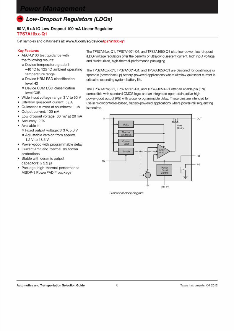
The TPS7A16xx-Q1, TPS7A1601-Q1, and TPS7A1650-Q1 ultra-low-power, low-dropout
(LDO) voltage regulators offer the benefits of ultralow quiescent current, high input voltage,and miniaturized, high-thermal-performance packaging.
The TPS7A16xx-Q1, TPS7A1601-Q1, and TPS7A1650-Q1 are designed for continuous orsporadic (power backup) battery-powered applications where ultralow quiescent current iscritical to extending system battery life.
The TPS7A16xx-Q1, TPS7A1601-Q1, and TPS7A1650-Q1 offer an enable pin (EN)compatible with standard CMOS logic and an integrated open-drain active-highpower-good output (PG) with a user-programmable delay. These pins are intended foruse in microcontroller-based, battery-powered applications where power-rail sequencingis required.
ThermalShutdown
CurrentLimit
EnableError Amp
IN
EN
OUT
FB
PassDevice
PowerGood
Control
DELAY
PG
UVLO
Functional block diagram.
8/15/2019 TI Selection Guide
http://slidepdf.com/reader/full/ti-selection-guide 9/49
➔
9 Automotive and Transportation Selection Guide Texas Instruments Q4 2012
Power Management
Low-Dropout Regulators (LDOs)
40 V, 20 uA IQ Low-Dropout 100/150 mA Linear RegulatorTPS7A66/69xx– Q1
Get samples and datasheets at: www.ti.com/sc/device/ tps7a6950-Q1
Key Features• AEC-Q100 test guidance with the
following results:
° Device temperature grade 1:
° –40 °C to 125 °C ambient operatingtemperature range
° Device HBM ESD classificationlevel H2
° Device CDM ESD classificationlevel C3B
• 4-V to 40-V Wide Input Voltage Range• LDO low Iq typ 20uA Iq• Stable with 2.2uF Low-ESR Ceramic
Output Capacitor• 150-mA Maximum Output Current• 2 μA (Typ) Low Shutdown/Sleep
Current• 2.5-V and 7-V Adjustable Output
Voltage• 2 % Output Voltage Tolerance• Integrated Fault Protection ° Short-Circuit/Over-Current
Protection ° Thermal Shutdown ° Low Input Voltage Tracking• MSOP-8 and SOIC-8
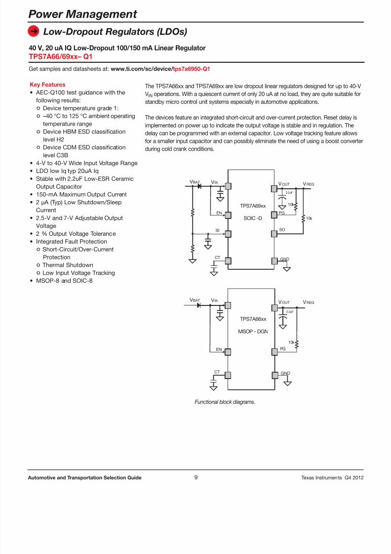
The TPS7A66xx and TPS7A69xx are low dropout linear regulators designed for up to 40-V
VIN operations. With a quiescent current of only 20 uA at no load, they are quite suitable forstandby micro control unit systems especially in automotive applications.
The devices feature an integrated short-circuit and over-current protection. Reset delay isimplemented on power up to indicate the output voltage is stable and in regulation. Thedelay can be programmed with an external capacitor. Low voltage tracking feature allowsfor a smaller input capacitor and can possibly eliminate the need of using a boost converterduring cold crank conditions.
Functional block diagrams.
V OUT
GND
V IN
PGEN
TPS7A69xx
SOIC -D
V REG
2.2uF
10k
SOSI
CT
10k
V BAT
V OUT V IN V REG
V BAT
GND
PGEN
TPS7A66xx
MSOP - DGN
2.2uF
10k
CT
8/15/2019 TI Selection Guide
http://slidepdf.com/reader/full/ti-selection-guide 10/49
➔
10 Automotive and Transportation Selection Guide Texas Instruments Q4 2012
Power Management
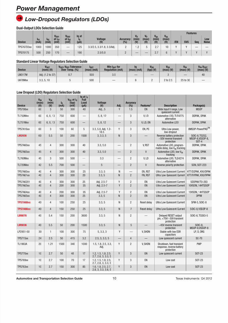
Low-Dropout Regulators (LDOs)Dual-Output LDOs Selection Guide
DeviceI01
(mA)I02
(mA)
VD01at I01 (mV)
VD02at I02 (mV)
Iq atI0
(µA)Voltage
(V)Accuracy
(%)
V0(min)
(V)
V0(max)
(V)
VIN(min)
(V)
VIN(max)
(V)
Features
/EN SVS SeqLow
Noise
TPS767D3xx 1000 1000 350 — 125 3.3/2.5, 3.3/1.8, 3.3/Adj. 2 1.2 5 2.7 10 Y Y — —
TPS70175 500 250 170 — 190 2.5/5.0 2 — — 2.7 6 Y Y Y Y
Standard Linear Voltage Regulators Selection Guide
DeviceV0UT
(nom) (V)V0UT/VREFTolerance
Over Temp. (%)I0UT
(max) (mA)Min I0UT for
Regulation (mA)Iq
(max) (mA)VD0
(typ) (V)VD0
(max) (V)VIN
(max) (V)VIN-VOUT
(max) (V)
LM317M Adj. (1.2 to 37) 0.7 500 3.5 — — 3 — 40
UA78Mxx 3.3, 5, 10 5 500 — 6 2 2 to 2.5 25 to 30 —
Low Dropout (LDO) Regulators Selection Guide
Device
VIN(max)
(V)
VIN(min)
(V) I0
(mA)
VD0 at I0(typ)(mV)
Iq at I 0Full
Load(µA)
Voltage(V) Adj.
Accuracy(%) Features 1 Description Package(s)
TPS798xx 60 3 50 300 40 Adj., 5 Y 1.5 EN Wide Input V range, Lowquiescent current
MSOP
TL750Mxx 60 6, 9, 13 750 600 — 5, 8, 12 — 3 V, LD Automotive LDO, TLE4275alternative
DDPAK, DPAK
TL751Mxx 60 6, 9, 13 750 600 — 5, 8, 12 — 3 V, LD, EN Automotive LDO DDPAK, DPA
TPS7A16xx 60 3 100 60 5 3.3, 5.0, Adj. 1.2-18.5
Y 3 EN, PG Ultra Low-power,low-dropout
8MSOP-PowerPADTM
LM2936 60 5.5 50 200 1500 3, 3.3, 5 N 3 — Reverse battery protection−50V reverse transient
protection
SOIC-8, TO252,MSOP-8,VSSOP-8,
SOT-4TPS7A60xx 45 4 300 300 40 3.3, 5.0 — 2 V, RST Automotive LDO, program-
mable delay, low VIN trackingDDPAK, DPAK
TPS7A65xx 45 4 300 300 40 3.3, 5.0 — 2 V Automotive LDO, low VIN tracking
DDPAK, DPAK
TL760Mxx 45 3 500 500 — 3.3 — 2 V, LD Automotive LDO, TLE4274alternative
DDPAK, DPAK
TL720Mxx 42 5.5 700 500 — 5 — 2 V Reverse polarity protection SON, SOT-223
TPS7A60xx 40 4 300 300 25 3.3, 5 N — EN, RST Ultra Low Quiescent Current KTT/D2PAK, KVUTPS7A61xx 40 4 300 300 20 3.3, 5 N 2 EN, RST Ultra Low Quiescent Current KTT/D2PAK, KVU
TPS7A6201 40 4 300 300 25 Adj. 2.5-7 Y 2 EN Ultra Low Quiescent Current 5DDPAK/TO-26TPS7A63xx 40 4 200 300 35 Adj. 2.5-7 Y 2 EN Ultra Low Quiescent Current 10VSON, 14HTSS
TPS7A64xx 40 4 200 300 35 Adj. 2.5-7 Y 2 EN Ultra Low Quiescent Current 10VSON, 14HTSSTPS7A65xx 40 4 300 300 25 3.3, 5 N 2 EN Ultra Low Quiescent Current 3PFM
TPS7A69xx 40 4 100 250 25 3.3, 5 N 2 Reset delay Ultra Low Quiescent Current SFM-5, SOIC-8
TPS7A66xx 40 4 150 250 25 3.3, 5 N 2 Reset delay Ultra Low Quiescent Current SOIC-8, VSSOP-8
LM9076 40 5.4 150 200 3600 3.3, 5 N 2 — Delayed RESET outputpin, +70V/−50V transient
protection
SOIC-8, TO263-5
LM9036 40 5.5 50 200 1500 3.3, 5 N 5 — −45V reverse transientprotection
SOIC-8,MSOP-8,VSSOP-8
LP2951-50 30 1 100 300 75 5, 3.3, 3 Y — V, SHDN Stable with low ESRcapacitors
LP, D, DRG
TPS715xx 24 2.5 50 415 3.2 2.5, 3, 3.3, 5 — 4 — Low quiescent current SC-70
TL1963A 20 1.21 1500 340 1000 1.5, 1.8, 2.5, 3.3, Adj.
Y 2 V, SHDN Shutdown, fast transientresponse, reverse battery
protection
PWP
TPS770xx 10 2.7 50 48 17 1.2, 1.5, 1,8, 2.5,2.7, 2.8, 3, 3.3, 5
Y 3 EN Low quiescent current SOT-23
TPS769xx 10 2.7 100 70 17 1.2, 1.5, 1.8, 2.5,2.7, 2.8, 3, 3.3, 5
Y 3 EN Low cost SOT-23
TPS763xx 10 2.7 150 300 85 1.6, 1.8, 2.5, 2.7,2.8, 3, 3.3, 3.8, 5
Y 3 EN Low cost SOT-23
8/15/2019 TI Selection Guide
http://slidepdf.com/reader/full/ti-selection-guide 11/49
➔
11 Automotive and Transportation Selection Guide Texas Instruments Q4 2012
Power Management
Low-Dropout Regulators (LDOs)
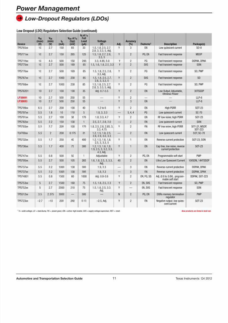
Low Dropout (LDO) Regulators Selection Guide (continued)
Device
VIN(max)
(V)
VIN(min)
(V) I0
(mA)
VD0 at I0(typ)(mV)
Iq at I 0Full
Load(µA)
Voltage(V) Adj.
Accuracy(%) Features 1 Description Package(s)
TPS765xx 10 2.7 150 85 33 1.5, 1.8, 2.5, 2.7,2.8, 3, 3.3, 5, Adj.
Y 3 EN Low quiescent current SO-8
TPS771xx 10 2.7 150 265 125 1.5, 1.8, 2.7, 2.8,3.3, 5
Y 2 PG, EN Fast transient response MSOP
TPS71Hxx 10 4.3 500 150 285 3.3, 4.85, 5.0 Y 2 PG Fast transient response DDPAK, DPAK TPS775xx 10 2.7 500 169 85 1.5, 1.6, 1.8, 2.5, 3.3 Y 2 SVS Fast transient response SON
TPS776xx 10 2.7 500 169 85 1.5, 1.8, 2.5, 2.8,3.3, Adj.
Y 2 PG Fast transient response SO, PWP
TPS767xx 10 2.7 1000 230 85 1.5, 1.8, 2.5, 2.7,2.8, 3, 3.3, 5
Y 2 SVS Fast transient response SO
TPS768xx 10 2.7 1000 230 85 1.5, 1.8, 2.5, 2.7,2.8, 3, 3.3, 5, Adj.
Y 2 PG Fast transient response SO, PWP
TPS76201 10 2.7 100 100 35 Adj. 0.7-5.5 Y 2 EN Low Output, Adjustable,Ultralow-Power
30TSSOP
LP38691 10 2.7 500 250 55 — Y 2 — — LLP-6LP38693 10 2.7 500 250 55 — Y 3 EN — LLP-6
TPS799xx 6.5 2.7 200 100 40 1.2 to 6 Y 2 EN High PSRR SOT-23
TPS797xx 5.5 1.8 10 110 5 1.8, 3, 3.3 — 5, 4, 4 PG Low quiescent current SC-70TPS791xx 5.5 2.7 100 38 170 1.8, 3.3, 4.7 Y 2 EN RF low noise; high PSRR SOT-23
TPS782xx 5.5 2.2 150 130 1 2.5, 2.7, 2.8, 3.0 — 2 EN Low quiescent current SON
TPS793xx 5.5 2.7 200 100 170 1.8, 2.5, 2.8, 2.85, 3,3.3, 4.75
Y 2 EN RF low noise, high PSRR SOT-23, MSOP,SOT-223
TLV700xx 5.5 2 200 0.175 31 1.2, 1.5, 1.8, 2.5,2.8, 2.9, 3.0, 3.3
— 2 EN Low quiescent current SOT, SC-70
TPS732xx 5.5 1.7 250 40 400 1.2, 1.5, 1.6, 1,8,2.5, 3, 3.3, 5
Y 1 EN Reverse current protection SOT-23, SON
TPS736xx 5.5 1.7 400 75 300 1.2, 1.5, 1.6, 1,8,1.9, 2.5, 3, 3.2, 3.3,
4.3, Adj.
Y 1 EN Cap free, low noise, reversecurrent protection
SOT-23
TPS747xx 5.5 0.8 500 50 1 Adjustable Y 2 PG, EN Programmable soft start PWP
TPS795xx 5.5 2.7 500 105 265 1.6, 1.8, 2.5, 3, 3.3, Adj.
40 2 EN Ultra Low Quiescent Current 10VSON, 14HTSS
TPS737xx 5.5 2.2 1000 130 300 1.9, 3.3 — 3 EN Reverse current protection DDPAK, DPAKTPS737xx 5.5 2.2 1000 130 300 1.9, 3.3 — 3 EN Reverse current protection DDPAK, DPAK
TPS74801 5.5 0.8 1500 60 1000 Adj. 0.8-3.6 Y 2 EN, PG, SS Adj. (0.8 to 3.6V), program-mable soft start
DDPAK, SOT-223
TPS753xx 5 2.7 1500 160 75 1.5, 1.8, 2.5, 3.3 Y 2 EN, SVS Fast transient response SO, PWP
TPS752xx 5 2.7 2000 210 75 1.5, 1.8, 2.5, 3.3, Adj.
Y — EN, SVS Fast transient response SON
TPS512xx 3.5 2.375 3000 — 500 — N 2 PG, EN DDRx memory terminationregulator
PWP
TPS723xx –2.7 –10 200 280 0.13 –2.5, Adj. Y 2 EN Negative output, low quies-cent current
SOT-23
1 V = wide voltage, LD = load dump, PG = power good, /EN = active high enable, SVS = supply voltage supervisor, RST = reset. New products are listed in bold red.
8/15/2019 TI Selection Guide
http://slidepdf.com/reader/full/ti-selection-guide 12/49
➔
12 Automotive and Transportation Selection Guide Texas Instruments Q4 2012
Power Management
Battery Management
3- to 6-Series Cell Lithium-Ion Battery Monitor and Secondary Protection ICbq76pl536A-Q1
Get samples and datasheets at: www.ti.com/sc/device/ bq76pl536A-Q1
Key Features
• Three- to six-series cell support,all chemistries hot-pluggable• Stackable vertical SPI interface• No isolation components required• High-speed SPI for data
communications• Dedicated fault signals• High-accuracy ADC: ° ±1 mV typical, ±3 mV max ° 14-bit resolution ° 6-μs conversion time• Nine ADC inputs: six cell voltages,
one six-cell “brick,” voltage, twotemperatures, one general-purposeinput
• Built-in comparators (secondaryprotector) for over-voltage,under-voltage and over-temperatureprotection
• Programmable thresholds anddelay times
• Supply voltage range from 5.5 Vto 30 V
• Low power:
° 12-μA sleep current typical
° 48-μA idle current typical• Integrated precision 5.0 V 3-mA LDO
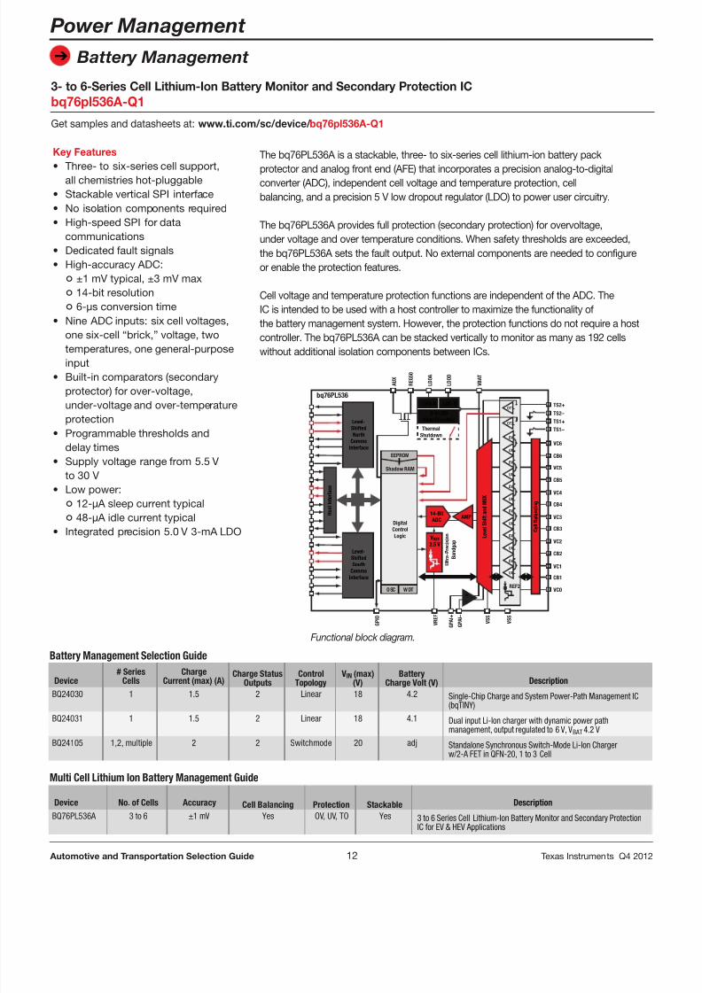
The bq76PL536A is a stackable, three- to six-series cell lithium-ion battery pack
protector and analog front end (AFE) that incorporates a precision analog-to-digitalconverter (ADC), independent cell voltage and temperature protection, cellbalancing, and a precision 5 V low dropout regulator (LDO) to power user circuitry.
The bq76PL536A provides full protection (secondary protection) for overvoltage,under voltage and over temperature conditions. When safety thresholds are exceeded,the bq76PL536A sets the fault output. No external components are needed to configureor enable the protection features.
Cell voltage and temperature protection functions are independent of the ADC. TheIC is intended to be used with a host controller to maximize the functionality ofthe battery management system. However, the protection functions do not require a hostcontroller. The bq76PL536A can be stacked vertically to monitor as many as 192 cellswithout additional isolation components between ICs.
TS2+
TS2–
TS1+
TS1–
VC6
A U X
G P I O
R E G 5 0
L D O A
L D O D
V B A T
V R E F
G P A I +
G P A I –
V S S
V S S
CB6
VC5
CB5
VC4
CB4
VC3
CB3
VC2
CB2
VC1
CB1
VC0
OT1
OT2
UV
OV
OV
OV
OV
OV
OV
UV
UV
UV
UV
UV
EEPROM
REF2
ThermalShutdown
bq76PL536LDO-A LDO-D
5-V LDO(User Circuitry)
14-BitADCDigitalControlLogic
OSC WDT
Level-ShiftedNorth
CommsInterface
Level-ShiftedSouth
CommsInterface
H o s t I n t e r f a c e
Shadow RAM
VREF2.5 V
AMP
+–
C e l l B a l a n c i n g
L e v e l
S h
i f t a n d M U X
U l t r a - P
r e c i s i o n
B a n d g a p
Battery Management Selection Guide
Device# Series
CellsCharge
Current (max) (A)Charge Status
Outputs
Control
Topology
VIN(max)
(V)
Battery
Charge Volt (V)Description
BQ24030 1 1.5 2 Linear 18 4.2 Single-Chip Charge and System Power-Path Management IC(bqTINY)
BQ24031 1 1.5 2 Linear 18 4.1 Dual input Li-Ion charger with dynamic power pathmanagement, output regulated to 6 V, VBAT 4.2 V
BQ24105 1,2, multiple 2 2 Switchmode 20 adj Standalone Synchronous Switch-Mode Li-Ion Chargerw/2-A FET in QFN-20, 1 to 3 Cell
Multi Cell Lithium Ion Battery Management Guide
Device No. of Cells Accuracy Cell Balancing Protection Stackable Description
BQ76PL536A 3 to 6 ±1 mV Yes OV, UV, TO Yes 3 to 6 Series Cell Lithium-Ion Battery Monitor and Secondary ProtectioIC for EV & HEV Applications
Functional block diagram.
8/15/2019 TI Selection Guide
http://slidepdf.com/reader/full/ti-selection-guide 13/49
➔
13 Automotive and Transportation Selection Guide Texas Instruments Q4 2012
Power Management
DC/DC Controllers and Converters
Multi-Rail Power Supply for Microcontrollers in Safety-Critical ApplicationsTPS65381-Q1
Get samples and datasheets at: www.ti.com/sc/device/ tps65381-q1
Key FeaturesMulti-rail power supply:
• Supports TMS570LS series16/32-bit RISC flash microcontroller
Supply rails:• Input voltage range:
° 5.8 V to 36 V (CAN, I/O, MCUcore, and sensor supplyregulators functional)
° 4.5 V to 5.8 V (3.3-V I/O andMCU core voltage functional)
• 6-V asynchronous switch-modepre-regulator with internal FET,1.5-A current limit, and temperatureprotection
• 5-V (CAN) supply voltage, linearregulator with internal FET, andtemperature protection
• 3.3-V or 5-V MCU I/O voltage, linearregulator with internal FET, andtemperature protection
• 0.8-V to 3.3-V adjustable MCU corevoltage, linear regulator controllerwith external FET
• Sensor supply: linear trackingregulator with tracking input,300-mA current limit, temperatureprotection, and protection againstshort to battery and short to ground
• Reverse battery protection withexternal FET allowing for Low-voltage operation down to 4.5 V
• Charge pump: Typ. 12 V abovebattery voltage
Power supply / system monitoring:• Under- and over-voltage
monitoring on all regulator outputs,
battery voltage, and internalsupplies• Self-check on all voltage monitoring
(during power up and after powerup initiated by external MCU)
• Independent voltage references forregulator references and voltagemonitoring voltage-monitoringcircuitry with separate batteryvoltage input
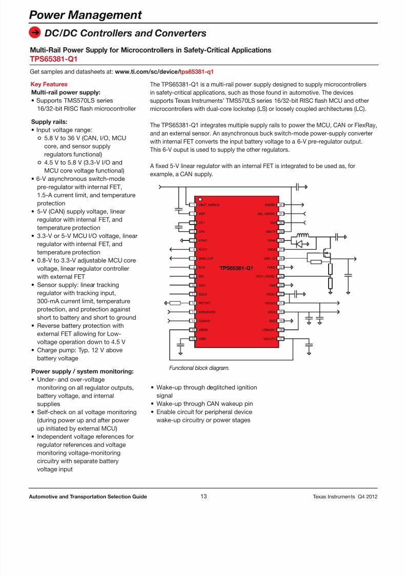
The TPS65381-Q1 is a multi-rail power supply designed to supply microcontrollersin safety-critical applications, such as those found in automotive. The devices
supports Texas Instruments’ TMS570LS series 16/32-bit RISC flash MCU and othermicrocontrollers with dual-core lockstep (LS) or loosely coupled architectures (LC).
The TPS65381-Q1 integrates multiple supply rails to power the MCU, CAN or FlexRay,and an external sensor. An asynchronous buck switch-mode power-supply converterwith internal FET converts the input battery voltage to a 6-V pre-regulator output.This 6-V ouput is used to supply the other regulators.
A fixed 5-V linear regulator with an internal FET is integrated to be used as, forexample, a CAN supply.
• Wake-up through deglitched ignition
signal• Wake-up through CAN wakeup pin• Enable circuit for peripheral device
wake-up circuitry or power stages
TPS65381-Q1
32
31
30
29
28
27
26
25
24
23
22
21
20
19
18
17
CP2
CP1
VCP
ERROR/WDI
PGND
VBAT_SAFIN G
CANWU
DIAG_OUT
VSIN
VSFB1 VTRACK1
VSOUT1
VDD6
VDD3/5
VDDIO
VDD1_G
SDN6
VBATP
IGN
VDD1_SENSE
GND
VDD5
ENDRV
SEL_VDD3/5
PGND
GND
1
2
4
13
14
3
15
16
5
6
7
8
9
10
11
12
SDO
NCS
SDI
SCLK
NRES
RSTEXT
Functional block diagram.
8/15/2019 TI Selection Guide
http://slidepdf.com/reader/full/ti-selection-guide 14/49
➔
14 Automotive and Transportation Selection Guide Texas Instruments Q4 2012
Power Management
DC/DC Controllers and Converters
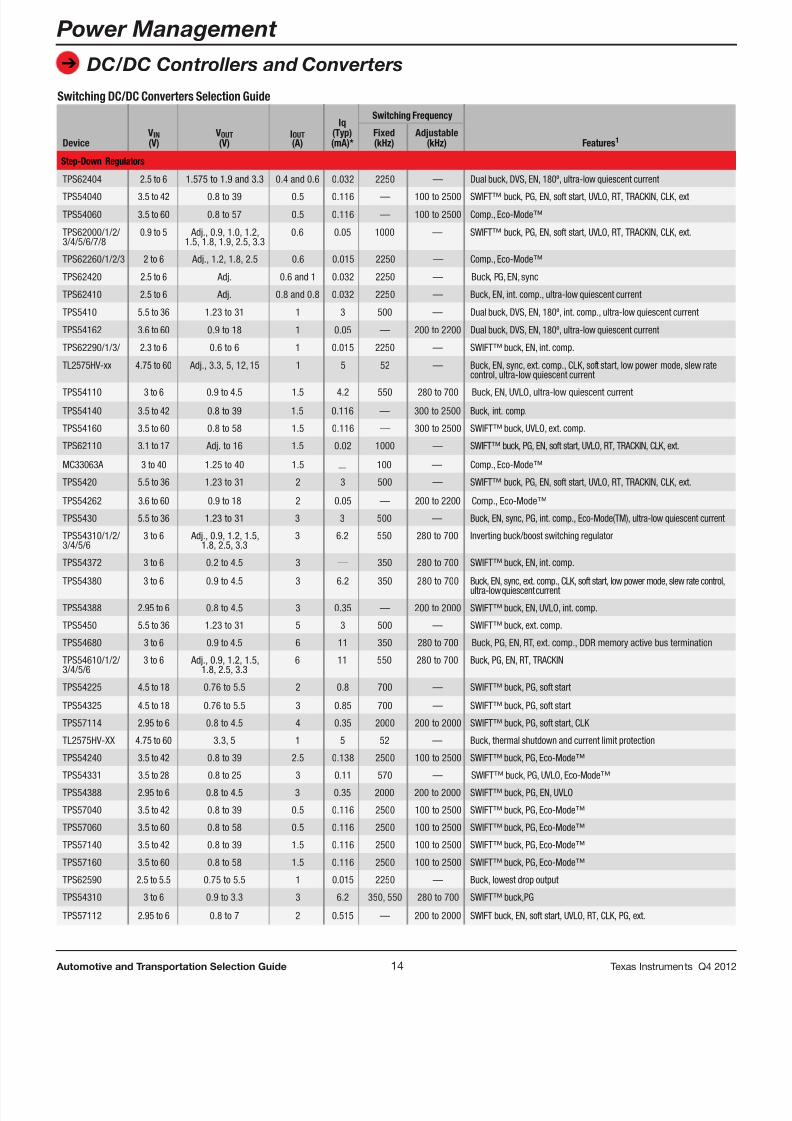
Switching DC/DC Converters Selection Guide
Iq(Typ)(mA)*
Switching Frequency
DeviceVIN(V)
VOUT(V)
IOUT(A)
Fixed(kHz)
Adjustable(kHz) Features1
Step-Down Regulators
TPS62404 2.5 to 6 1.575 to 1.9 and 3.3 0.4 and 0.6 0.032 2250 — Dual buck, DVS, EN, 180º, ultra-low quiescent current
TPS54040 3.5 to 42 0.8 to 39 0.5 0.116 — 100 to 2500 SWIFT™ buck, PG, EN, soft start, UVLO, RT, TRACKIN, CLK, ext
TPS54060 3.5 to 60 0.8 to 57 0.5 0.116 — 100 to 2500 Comp., Eco-Mode™
TPS62000/1/2/ 3/4/5/6/7/8
0.9 to 5 Adj., 0.9, 1.0, 1.2,1.5, 1.8, 1.9, 2.5, 3.3
0.6 0.05 1000 — SWIFT™ buck, PG, EN, soft start, UVLO, RT, TRACKIN, CLK, ext.
TPS62260/1/2/3 2 to 6 Adj., 1.2, 1.8, 2.5 0.6 0.015 2250 — Comp., Eco-Mode™
TPS62420 2.5 to 6 Adj. 0.6 and 1 0.032 2250 — Buck, PG, EN, sync
TPS62410 2.5 to 6 Adj. 0.8 and 0.8 0.032 2250 — Buck, EN, int. comp., ultra-low quiescent current
TPS5410 5.5 to 36 1.23 to 31 1 3 500 — Dual buck, DVS, EN, 180º, int. comp., ultra-low quiescent current
TPS54162 3.6 to 60 0.9 to 18 1 0.05 — 200 to 2200 Dual buck, DVS, EN, 180º, ultra-low quiescent current
TPS62290/1/3/ 2.3 to 6 0.6 to 6 1 0.015 2250 — SWIFT™ buck, EN, int. comp.
TL2575HV-xx 4.75 to 60 Adj., 3.3, 5, 12, 15 1 5 52 — Buck, EN, sync, ext. comp., CLK, soft start, low power mode, slew ratecontrol, ultra-low quiescent current
TPS54110 3 to 6 0.9 to 4.5 1.5 4.2 550 280 to 700 Buck, EN, UVLO, ultra-low quiescent current
TPS54140 3.5 to 42 0.8 to 39 1.5 0.116 — 300 to 2500 Buck, int. comp.
TPS54160 3.5 to 60 0.8 to 58 1.5 0.116 — 300 to 2500 SWIFT™ buck, UVLO, ext. comp.
TPS62110 3.1 to 17 Adj. to 16 1.5 0.02 1000 — SWIFT™ buck, PG, EN, soft start, UVLO, RT, TRACKIN, CLK, ext.
MC33063A 3 to 40 1.25 to 40 1.5 — 100 — Comp., Eco-Mode™
TPS5420 5.5 to 36 1.23 to 31 2 3 500 — SWIFT™ buck, PG, EN, soft start, UVLO, RT, TRACKIN, CLK, ext.
TPS54262 3.6 to 60 0.9 to 18 2 0.05 — 200 to 2200 Comp., Eco-Mode™
TPS5430 5.5 to 36 1.23 to 31 3 3 500 — Buck, EN, sync, PG, int. comp., Eco-Mode(TM), ultra-low quiescent curre
TPS54310/1/2/ 3/4/5/6
3 to 6 Adj., 0.9, 1.2, 1.5,1.8, 2.5, 3.3
3 6.2 550 280 to 700 Inverting buck/boost switching regulator
TPS54372 3 to 6 0.2 to 4.5 3 — 350 280 to 700 SWIFT™ buck, EN, int. comp.
TPS54380 3 to 6 0.9 to 4.5 3 6.2 350 280 to 700 Buck, EN, sync, ext. comp., CLK, soft start, low power mode, slew rate controultra-low quiescent current
TPS54388 2.95 to 6 0.8 to 4.5 3 0.35 — 200 to 2000 SWIFT™ buck, EN, UVLO, int. comp.
TPS5450 5.5 to 36 1.23 to 31 5 3 500 — SWIFT™ buck, ext. comp.
TPS54680 3 to 6 0.9 to 4.5 6 11 350 280 to 700 Buck, PG, EN, RT, ext. comp., DDR memory active bus termination
TPS54610/1/2/ 3/4/5/6
3 to 6 Adj., 0.9, 1.2, 1.5,1.8, 2.5, 3.3
6 11 550 280 to 700 Buck, PG, EN, RT, TRACKIN
TPS54225 4.5 to 18 0.76 to 5.5 2 0.8 700 — SWIFT™ buck, PG, soft start
TPS54325 4.5 to 18 0.76 to 5.5 3 0.85 700 — SWIFT™ buck, PG, soft start
TPS57114 2.95 to 6 0.8 to 4.5 4 0.35 2000 200 to 2000 SWIFT™ buck, PG, soft start, CLK
TL2575HV-XX 4.75 to 60 3.3, 5 1 5 52 — Buck, thermal shutdown and current limit protection
TPS54240 3.5 to 42 0.8 to 39 2.5 0.138 2500 100 to 2500 SWIFT™ buck, PG, Eco-Mode™
TPS54331 3.5 to 28 0.8 to 25 3 0.11 570 — SWIFT™ buck, PG, UVLO, Eco-Mode™TPS54388 2.95 to 6 0.8 to 4.5 3 0.35 2000 200 to 2000 SWIFT™ buck, PG, EN, UVLO
TPS57040 3.5 to 42 0.8 to 39 0.5 0.116 2500 100 to 2500 SWIFT™ buck, PG, Eco-Mode™
TPS57060 3.5 to 60 0.8 to 58 0.5 0.116 2500 100 to 2500 SWIFT™ buck, PG, Eco-Mode™
TPS57140 3.5 to 42 0.8 to 39 1.5 0.116 2500 100 to 2500 SWIFT™ buck, PG, Eco-Mode™
TPS57160 3.5 to 60 0.8 to 58 1.5 0.116 2500 100 to 2500 SWIFT™ buck, PG, Eco-Mode™
TPS62590 2.5 to 5.5 0.75 to 5.5 1 0.015 2250 — Buck, lowest drop output
TPS54310 3 to 6 0.9 to 3.3 3 6.2 350, 550 280 to 700 SWIFT™ buck,PG
TPS57112 2.95 to 6 0.8 to 7 2 0.515 — 200 to 2000 SWIFT buck, EN, soft start, UVLO, RT, CLK, PG, ext.
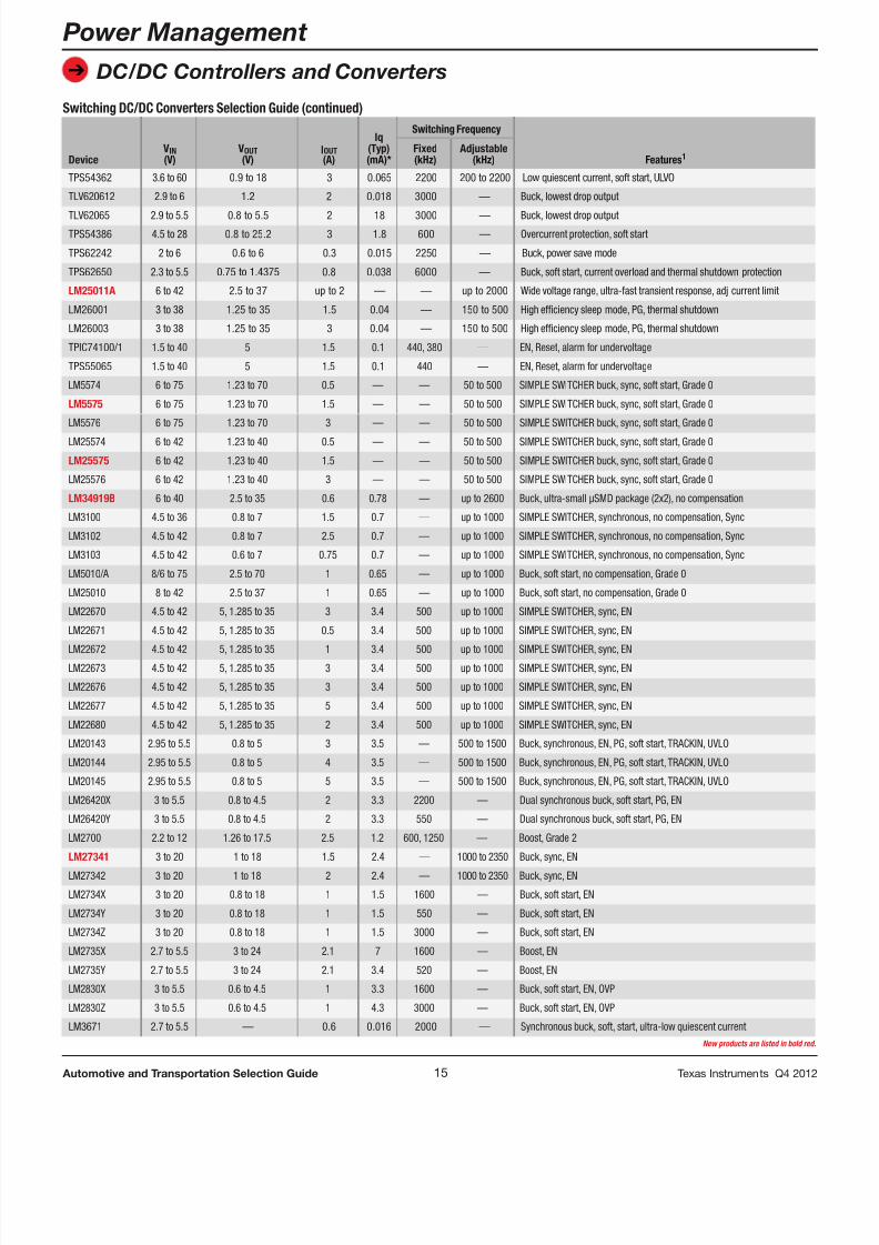
8/15/2019 TI Selection Guide
http://slidepdf.com/reader/full/ti-selection-guide 15/49
➔
15 Automotive and Transportation Selection Guide Texas Instruments Q4 2012
Power Management
DC/DC Controllers and Converters
Switching DC/DC Converters Selection Guide (continued)
Iq(Typ)(mA)*
Switching Frequency
DeviceVIN(V)
VOUT(V)
IOUT(A)
Fixed(kHz)
Adjustable(kHz) Features1
TPS54362 3.6 to 60 0.9 to 18 3 0.065 2200 200 to 2200 Low quiescent current, soft start, ULVO
TLV620612 2.9 to 6 1.2 2 0.018 3000 — Buck, lowest drop output
TLV62065 2.9 to 5.5 0.8 to 5.5 2 18 3000 — Buck, lowest drop outputTPS54386 4.5 to 28 0.8 to 25.2 3 1.8 600 — Overcurrent protection, soft start
TPS62242 2 to 6 0.6 to 6 0.3 0.015 2250 — Buck, power save mode
TPS62650 2.3 to 5.5 0.75 to 1.4375 0.8 0.038 6000 — Buck, soft start, current overload and thermal shutdown protection
LM25011A 6 to 42 2.5 to 37 up to 2 — — up to 2000 Wide voltage range, ultra-fast transient response, adj current limit
LM26001 3 to 38 1.25 to 35 1.5 0.04 — 150 to 500 High efciency sleep mode, PG, thermal shutdown
LM26003 3 to 38 1.25 to 35 3 0.04 — 150 to 500 High efciency sleep mode, PG, thermal shutdown
TPIC74100/1 1.5 to 40 5 1.5 0.1 440, 380 — EN, Reset, alarm for undervoltage
TPS55065 1.5 to 40 5 1.5 0.1 440 — EN, Reset, alarm for undervoltage
LM5574 6 to 75 1.23 to 70 0.5 — — 50 to 500 SIMPLE SWITCHER buck, sync, soft start, Grade 0
LM5575 6 to 75 1.23 to 70 1.5 — — 50 to 500 SIMPLE SWITCHER buck, sync, soft start, Grade 0
LM5576 6 to 75 1.23 to 70 3 — — 50 to 500 SIMPLE SWITCHER buck, sync, soft start, Grade 0
LM25574 6 to 42 1.23 to 40 0.5 — — 50 to 500 SIMPLE SWITCHER buck, sync, soft start, Grade 0
LM25575 6 to 42 1.23 to 40 1.5 — — 50 to 500 SIMPLE SWITCHER buck, sync, soft start, Grade 0
LM25576 6 to 42 1.23 to 40 3 — — 50 to 500 SIMPLE SWITCHER buck, sync, soft start, Grade 0
LM34919B 6 to 40 2.5 to 35 0.6 0.78 — up to 2600 Buck, ultra-small μSMD package (2x2), no compensation
LM3100 4.5 to 36 0.8 to 7 1.5 0.7 — up to 1000 SIMPLE SWITCHER, synchronous, no compensation, Sync
LM3102 4.5 to 42 0.8 to 7 2.5 0.7 — up to 1000 SIMPLE SWITCHER, synchronous, no compensation, Sync
LM3103 4.5 to 42 0.6 to 7 0.75 0.7 — up to 1000 SIMPLE SWITCHER, synchronous, no compensation, Sync
LM5010/A 8/6 to 75 2.5 to 70 1 0.65 — up to 1000 Buck, soft start, no compensation, Grade 0
LM25010 8 to 42 2.5 to 37 1 0.65 — up to 1000 Buck, soft start, no compensation, Grade 0
LM22670 4.5 to 42 5, 1.285 to 35 3 3.4 500 up to 1000 SIMPLE SWITCHER, sync, EN
LM22671 4.5 to 42 5, 1.285 to 35 0.5 3.4 500 up to 1000 SIMPLE SWITCHER, sync, EN
LM22672 4.5 to 42 5, 1.285 to 35 1 3.4 500 up to 1000 SIMPLE SWITCHER, sync, EN
LM22673 4.5 to 42 5, 1.285 to 35 3 3.4 500 up to 1000 SIMPLE SWITCHER, sync, EN
LM22676 4.5 to 42 5, 1.285 to 35 3 3.4 500 up to 1000 SIMPLE SWITCHER, sync, EN
LM22677 4.5 to 42 5, 1.285 to 35 5 3.4 500 up to 1000 SIMPLE SWITCHER, sync, EN
LM22680 4.5 to 42 5, 1.285 to 35 2 3.4 500 up to 1000 SIMPLE SWITCHER, sync, EN
LM20143 2.95 to 5.5 0.8 to 5 3 3.5 — 500 to 1500 Buck, synchronous, EN, PG, soft start, TRACKIN, UVLO
LM20144 2.95 to 5.5 0.8 to 5 4 3.5 — 500 to 1500 Buck, synchronous, EN, PG, soft start, TRACKIN, UVLO
LM20145 2.95 to 5.5 0.8 to 5 5 3.5 — 500 to 1500 Buck, synchronous, EN, PG, soft start, TRACKIN, UVLO
LM26420X 3 to 5.5 0.8 to 4.5 2 3.3 2200 — Dual synchronous buck, soft start, PG, EN
LM26420Y 3 to 5.5 0.8 to 4.5 2 3.3 550 — Dual synchronous buck, soft start, PG, EN
LM2700 2.2 to 12 1.26 to 17.5 2.5 1.2 600, 1250 — Boost, Grade 2
LM27341 3 to 20 1 to 18 1.5 2.4 — 1000 to 2350 Buck, sync, ENLM27342 3 to 20 1 to 18 2 2.4 — 1000 to 2350 Buck, sync, EN
LM2734X 3 to 20 0.8 to 18 1 1.5 1600 — Buck, soft start, EN
LM2734Y 3 to 20 0.8 to 18 1 1.5 550 — Buck, soft start, EN
LM2734Z 3 to 20 0.8 to 18 1 1.5 3000 — Buck, soft start, EN
LM2735X 2.7 to 5.5 3 to 24 2.1 7 1600 — Boost, EN
LM2735Y 2.7 to 5.5 3 to 24 2.1 3.4 520 — Boost, EN
LM2830X 3 to 5.5 0.6 to 4.5 1 3.3 1600 — Buck, soft start, EN, OVP
LM2830Z 3 to 5.5 0.6 to 4.5 1 4.3 3000 — Buck, soft start, EN, OVP
LM3671 2.7 to 5.5 — 0.6 0.016 2000 — Synchronous buck, soft, start, ultra-low quiescent currentNew products are listed in bold red.
8/15/2019 TI Selection Guide
http://slidepdf.com/reader/full/ti-selection-guide 16/49
➔
16 Automotive and Transportation Selection Guide Texas Instruments Q4 2012
Power Management
DC/DC Controllers and Converters
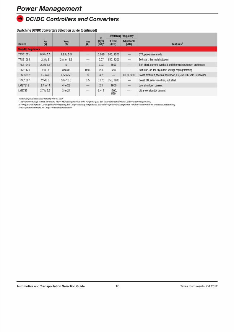
Switching DC/DC Converters Selection Guide (continued)
Iq(Typ)(mA)*
Switching Frequency
DeviceVIN(V)
VOUT(V)
IOUT(A)
Fixed(kHz)
Adjustable(kHz) Features1
Step-Up Regulators
TPS6107x 0.9 to 5.5 1.8 to 5.5 — 0.019 600, 1200 — OTP, powersave mode
TPS61085 2.3 to 6 2.8 to 18.5 — 0.07 650, 1200 — Soft start, thermal shutdown
TPS61240 2.3 to 5.5 5 — 0.03 3500 — Soft start, current overload and thermal shutdown protection
TPS61170 3 to 18 3 to 38 0.96 2.3 1200 — Soft start, on-the-y output voltage reprogramming
TPS55332 1.5 to 40 2.5 to 50 3 4.2 — 80 to 2200 Boost, soft start, thermal shutdown, EN, ext CLK, volt. Supervisor
TPS61087 2.5 to 6 3 to 18.5 0.5 0.075 650, 1200 — Boost, EN, selectable freq, soft start
LM27313 2.7 to 14 4 to 28 — 2.1 1600 — Low shutdown current
LM2735 2.7 to 5.5 3 to 24 — 3.4, 7 1700,550
— Ultra-low standby current
*Assumes Iq means standby (regulating with no load)1 DVS=dynamic voltage scaling, EN=enable, 180º = 180º out of phase operation, PG=power good, Soft start=adjustable slow start, UVLO=undervoltage lockout,RT=Frequency setting pin, CLK=to synchronize frequency, Ext. Comp.=externally compensated, Eco-mode=high efficiency at light load, TRACKIN=ext reference for simultaneous sequencing,SYNC=synchronization pin, Int. Comp. = internally compensated
8/15/2019 TI Selection Guide
http://slidepdf.com/reader/full/ti-selection-guide 17/49
➔
17 Automotive and Transportation Selection Guide Texas Instruments Q4 2012
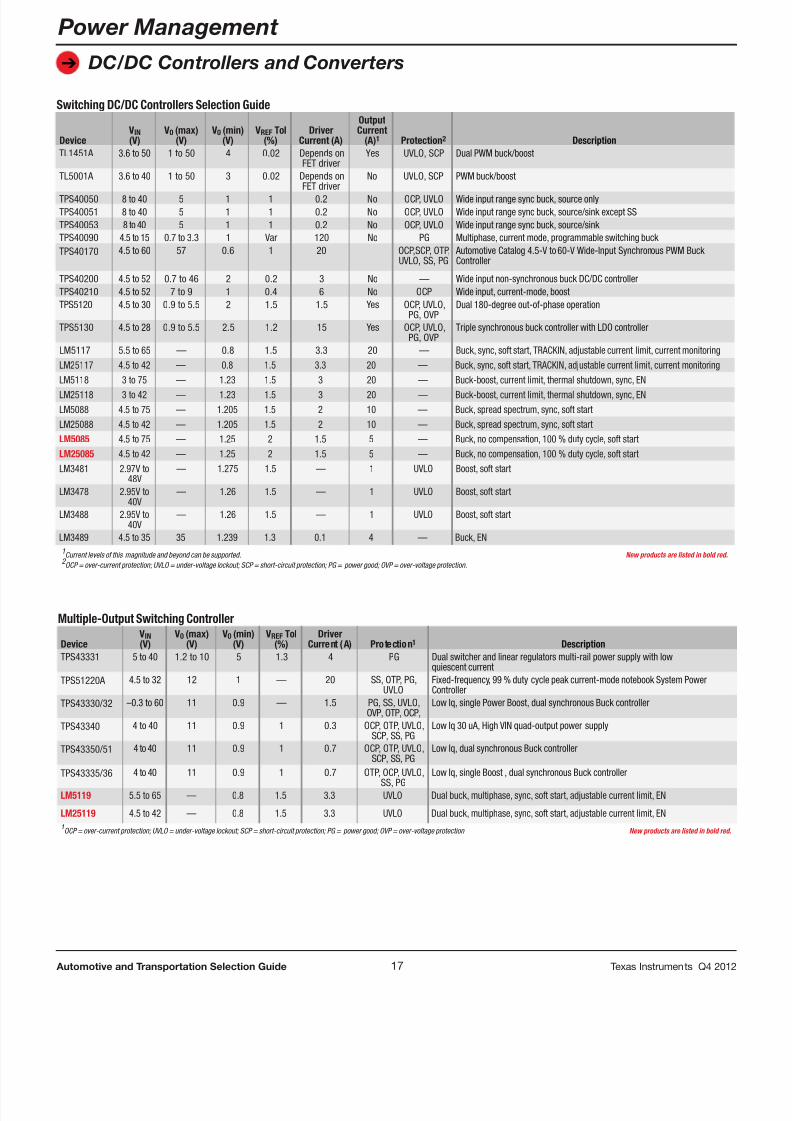
Switching DC/DC Controllers Selection Guide
DeviceVIN(V)
V0 (max)(V)
V0 (min)(V)
VREF Tol(%)
DriverCurrent (A)
OutputCurrent
(A)1 Protection 2 DescriptionTL1451A 3.6 to 50 1 to 50 4 0.02 Depends on
FET driver Yes UVLO, SCP Dual PWM buck/boost
TL5001A 3.6 to 40 1 to 50 3 0.02 Depends onFET driver
No UVLO, SCP PWM buck/boost
TPS40050 8 to 40 5 1 1 0.2 No OCP, UVLO Wide input range sync buck, source onlyTPS40051 8 to 40 5 1 1 0.2 No OCP, UVLO Wide input range sync buck, source/sink except SSTPS40053 8 to 40 5 1 1 0.2 No OCP, UVLO Wide input range sync buck, source/sink TPS40090 4.5 to 15 0.7 to 3.3 1 Var 120 No PG Multiphase, current mode, programmable switching buck TPS40170 4.5 to 60 57 0.6 1 20 OCP,SCP, OTP,
UVLO, SS, PG Automotive Catalog 4.5-V to 60-V Wide-Input Synchronous PWM BuckController
TPS40200 4.5 to 52 0.7 to 46 2 0.2 3 No — Wide input non-synchronous buck DC/DC controllerTPS40210 4.5 to 52 7 to 9 1 0.4 6 No OCP Wide input, current-mode, boostTPS5120 4.5 to 30 0.9 to 5.5 2 1.5 1.5 Yes OCP, UVLO,
PG, OVPDual 180-degree out-of-phase operation
TPS5130 4.5 to 28 0.9 to 5.5 2.5 1.2 15 Yes OCP, UVLO,PG, OVP
Triple synchronous buck controller with LDO controller
LM5117 5.5 to 65 — 0.8 1.5 3.3 20 — Buck, sync, soft start, TRACKIN, adjustable current limit, current monitorinLM25117 4.5 to 42 — 0.8 1.5 3.3 20 — Buck, sync, soft start, TRACKIN, adjustable current limit, current monitorinLM5118 3 to 75 — 1.23 1.5 3 20 — Buck-boost, current limit, thermal shutdown, sync, ENLM25118 3 to 42 — 1.23 1.5 3 20 — Buck-boost, current limit, thermal shutdown, sync, ENLM5088 4.5 to 75 — 1.205 1.5 2 10 — Buck, spread spectrum, sync, soft startLM25088 4.5 to 42 — 1.205 1.5 2 10 — Buck, spread spectrum, sync, soft startLM5085 4.5 to 75 — 1.25 2 1.5 5 — Buck, no compensation, 100 % duty cycle, soft startLM25085 4.5 to 42 — 1.25 2 1.5 5 — Buck, no compensation, 100 % duty cycle, soft startLM3481 2.97V to
48V— 1.275 1.5 — 1 UVLO Boost, soft start
LM3478 2.95V to40V
— 1.26 1.5 — 1 UVLO Boost, soft start
LM3488 2.95V to40V
— 1.26 1.5 — 1 UVLO Boost, soft start
LM3489 4.5 to 35 35 1.239 1.3 0.1 4 — Buck, EN1Current levels of this magnitude and beyond can be supported. New products are listed in bold red. 2 OCP = over-current protection; UVLO = under-voltage lockout; SCP = short-circuit protection; PG = power good; OVP = over-voltage protection.
Multiple-Output Switching Controller
DeviceVIN(V)
V0 (max)(V)
V0 (min)(V)
VREF Tol(%)
DriverCurrent (A) Pro tection 1 Description
TPS43331 5 to 40 1.2 to 10 5 1.3 4 PG Dual switcher and linear regulators multi-rail power supply with lowquiescent current
TPS51220A 4.5 to 32 12 1 — 20 SS, OTP, PG,UVLO
Fixed-frequency, 99 % duty cycle peak current-mode notebook System PowerController
TPS43330/32 –0.3 to 60 11 0.9 — 1.5 PG, SS, UVLO,OVP, OTP, OCP,
Low Iq, single Power Boost, dual synchronous Buck controller
TPS43340 4 to 40 11 0.9 1 0.3 OCP, OTP, UVLO,SCP, SS, PG
Low Iq 30 uA, High VIN quad-output power supply
TPS43350/51 4 to 40 11 0.9 1 0.7 OCP, OTP, UVLO,SCP, SS, PG
Low Iq, dual synchronous Buck controller
TPS43335/36 4 to 40 11 0.9 1 0.7 OTP, OCP, UVLO,SS, PG Low Iq, single Boost , dual synchronous Buck controller
LM5119 5.5 to 65 — 0.8 1.5 3.3 UVLO Dual buck, multiphase, sync, soft start, adjustable current limit, EN
LM25119 4.5 to 42 — 0.8 1.5 3.3 UVLO Dual buck, multiphase, sync, soft start, adjustable current limit, EN1OCP = over-current protection; UVLO = under-voltage lockout; SCP = short-circuit protection; PG = power good; OVP = over-voltage protection New products are listed in bold red.
Power Management
DC/DC Controllers and Converters
8/15/2019 TI Selection Guide
http://slidepdf.com/reader/full/ti-selection-guide 18/49
➔
18 Automotive and Transportation Selection Guide Texas Instruments Q4 2012
Power Management
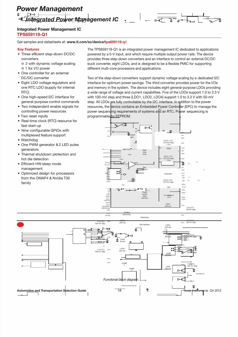
Integrated Power Management IC
Integrated Power Management ICTPS659119-Q1
Get samples and datasheets at: www.ti.com/sc/device/ tps659119-q1
Key Features• Three efficient step-down DC/DC
converters ° 2 with dynamic voltage scaling ° 1 for I/O power• One controller for an external
DC/DC converter• Eight LDO voltage regulators and
one RTC LDO (supply for internalRTC)
• One high-speed I2C interface forgeneral-purpose control commands
• Two independent enable signals forcontrolling power resources
• Two reset inputs• Real-time clock (RTC) resource for
fast start-up• Nine configurable GPIOs with
multiplexed feature support• Watchdog• One PWM generator & 2 LED pulse
generators• Thermal shutdown protection and
hot die detection• Efficient HW sleep mode
management
• Optimized design for processorsfrom the OMAP4 & Nvidia T30family
The TPS659119-Q1 is an integrated power management IC dedicated to applicationspowered by a 5-V input, and which require multiple output power rails. The device
provides three step-down converters and an interface to control an external DC/DCbuck converter, eight LDOs, and is designed to be a flexible PMIC for supportingdifferent multi-core processors and applications.
Two of the step-down converters support dynamic voltage scaling by a dedicated I2Cinterface for optimum power savings. The third converter provides power for the I/Osand memory in the system. The device includes eight general-purpose LDOs providinga wide range of voltage and current capabilities. Five of the LDOs support 1.0 to 3.3 Vwith 100-mV step and three (LDO1, LDO2, LDO4) support 1.0 to 3.3 V with 50-mVstep. All LDOs are fully controllable by the I2C interface. In addition to the powerresources, the device contains an Embedded Power Controller (EPC) to manage thepower sequencing requirements of systems and an RTC. Power sequencing is
programmable by EEPROM.
Functional block diagram.
SWCS062-001
VFB2
PWRON
VREF
Test interface
CLK32KOUT
3
OSCXTAL16M
OSCEXT32K
TESTV
SLEEP
NRESPWRON
PWRDN
BOOT1
(LDO )
SDA_SDI
VRTCandPOR
(LDO)
BACKUPMgmt
3
(SMPS)
5V
VCC6
VCC3
VCC5
VCC7
VDDIO
AGND AGND
DGND
SCL_SCKI C2
C BB
LDO1320 mA
LDO2
LDO7
LDO8
LDO3200 mA
LDO3
LDO4
3
(SMPS)
LDO5
VCC4
VCCS
Watchdog
Analogreferences
TRIP
DRVH
DRVL
SW
VOUT
V5IN
GNDC
VBST
NRESPWRON2
HDRST
REFGND
VFB
PWRHOLD
LDO2320 mA
LDO450 mA
LDO5300 mA
LDO8300 mA
LDO7300 mA
LDO6
LDO6300 mA
V B A C K U P
EN1
EN2
I C2
VDD1
VDD2
VIO
1.5/1.8/2.5/3.3V1.5 A
R trip
C
C
1
boost
CV5IN
C
C
o
VIN
GPIO0GPIO1GPIO2GPIO3
GPIO4GPIO5GPIO6GPIO7GPIO8
INT1
1 to 3.3 V,50-mV step
1 to 3.3 V,100-mV step
1 to 3.3 V,100-mV step
COMP1
COMP2
VCC1
SW1
GND1
VFB1
VCC2
SW2
GND2
3
VRTC
VCCIO
SWIO
GNDIO
VFBIO
LDO1
VDDIO
1 to 3.3 V,50-mV step
1 to 3.3 V,50-mV step
1 to 3.3 V,100-mV step
1 to 3.3 V,100-mV step
1 to 3.3 V,100-mV step
Realtimeclock
Buscontrol
Power controlstate
machine
0.6 to 1.5 V,12.5-mV step,
1.5 A
0.6 to 1.5 V,12.5-mV step,
1.5 A
0.6 to 1.4 V,12.5-mV step
Controller
16M XTAL
8/15/2019 TI Selection Guide
http://slidepdf.com/reader/full/ti-selection-guide 19/49
➔
19 Automotive and Transportation Selection Guide Texas Instruments Q4 2012
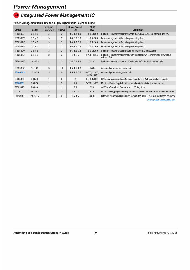
Power Management Multi-Channel IC (PMIC) Solutions Selection Guide
Device VIN (V)# DC-DC
Converters # LDOsDriver Current
(A)LDO IO (mA) Description
TPS65023 2.5 to 6 3 3 1.5, 1.2, 1.0 1x30, 2x200 6-channel power management IC with 3DC/DCs, 3 LDOs, I2C interface and DVS
TPS650250 2.5 to 6 3 3 1.6, 0.8, 0.8 1x30, 2x200 Power management IC for Li-Ion powered systems
TPS650243 2.5 to 6 3 3 1.6, 1.6, 0.8 1x30, 2x200 Power management IC for Li-Ion powered systems
TPS650241 2.5 to 6 3 3 1.6, 1.6, 0.8 1x30, 2x200 Power management IC for Li-Ion powered systemsTPS650244 2.5 to 6 3 3 1.6, 1.0, 0.8 1x30, 2x200 6-channel power management unit for single cell Li-Ion systems
TPS65053 2.5 to 6 2 3 1.0, 0.6 1x400, 2x200 5-channel power management IC with two step down converters and 3 low-inputvoltage LDO
TPS650732 2.8 to 6.3 3 2 0.6, 0.6, 1.5 2x200 5-channel power management IC with 3 DC/DCs, 2 LDOs in 6x6mm QFN
TPS658629 3 to 16.5 3 11 1.5, 1.5, 1.3 11x700 Advanced power management unit
TPS659119 2.7 to 5.5 3 8 1.5, 1.5, 0.5 4x300, 2x320,1x200, 1x50
Advanced power management unit
TPS65300 5.6 to 40 1 3 2 2x20, 1x300 3MHz step-down regulator, 1x linear regulator and 2x linear regulator controller
TPS65381 5.8 to 36 1 3 1.5 2x300, 1x600 Multi-Rail Power Supply for Microcontrollers in Safety Critical Appl ications
TPS65320 3.6 to 40 1 1 3.5 350 40V Step-Down Buck Converter and LDO Regulator
LP3907 2.8 to 5.5 2 2 1.0, 0.6 2x300 Multi-function, programmable power management unit with I2C-compatible interfac
LM26480 2.8 to 5.5 2 2 1.5, 1.5 2x300 Externally Programmable Dual High-Current Step-Down DC/DC and Dual Linear Regul
Preview products are listed in bold blue.
Power Management
Integrated Power Management IC
8/15/2019 TI Selection Guide
http://slidepdf.com/reader/full/ti-selection-guide 20/49
➔
20 Automotive and Transportation Selection Guide Texas Instruments Q4 2012
Power Management
LED Drivers
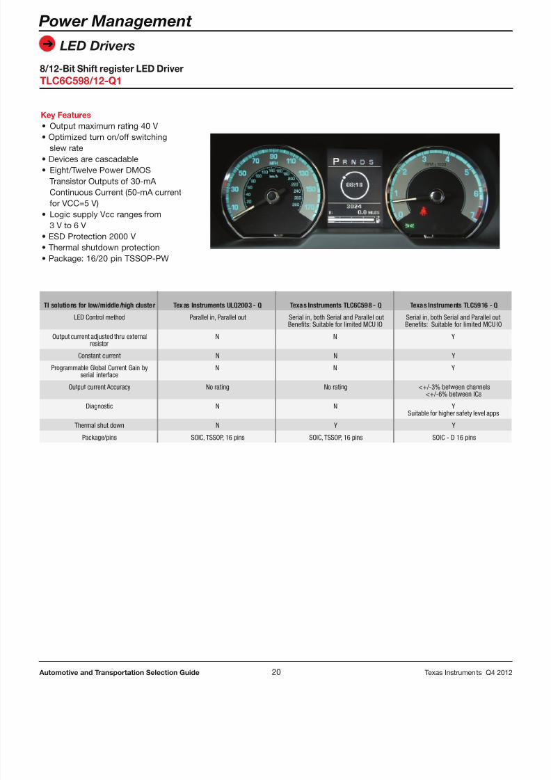
8/12-Bit Shift register LED DriverTLC6C598/12-Q1
Key Features• Output maximum rating 40 V• Optimized turn on/off switching
slew rate• Devices are cascadable• Eight/Twelve Power DMOS
Transistor Outputs of 30-mAContinuous Current (50-mA currentfor VCC=5 V)
• Logic supply Vcc ranges from3 V to 6 V
• ESD Protection 2000 V• Thermal shutdown protection• Package: 16/20 pin TSSOP-PW
TI solutions for low/middle /high cluste r Texas Instruments ULQ2003 - Q Texas Instruments TLC6C598 - Q Texas Instruments TLC5916 - Q
LED Control method Parallel in, Parallel out Serial in, both Serial and Parallel outBenets: Suitable for limited MCU IO
Serial in, both Serial and Parallel outBenets: Suitable for limited MCU IO
Output current adjusted thru externalresistor
N N Y
Constant current N N Y
Programmable Global Current Gain byserial interface
N N Y
Output current Accuracy No rating No rating <+/-3% between channels<+/-6% between ICs
Diagnostic N N YSuitable for higher safety level apps
Thermal shut down N Y Y
Package/pins SOIC, TSSOP, 16 pins SOIC, TSSOP, 16 pins SOIC - D 16 pins
8/15/2019 TI Selection Guide
http://slidepdf.com/reader/full/ti-selection-guide 21/49
➔
21 Automotive and Transportation Selection Guide Texas Instruments Q4 2012
Power Management
LED Drivers
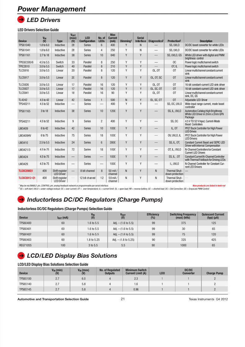
Inductorless DC/DC Regulators (Charge Pumps) Selection Guide
Device IOUT(mA)VIN(V)
VOUT (V)
Efciency(%)
Switching Frequency(max) (kHz)
Quiescent Current(typ) (µA)
TPS60400 60 1.6 to 5.5 Adj. – (1.6 to 5.5) 99 375 125
TPS60401 60 1.6 to 5.5 Adj. – (1.6 to 5.5) 99 30 65
TPS60402 60 1.6 to 5.5 Adj. – (1.6 to 5.5) 99 75 120
TPS60403 60 1.8 to 5.25 Adj. – (1.8 to 5.25) 90 325 425REG71055 100 3 to 5.5 5.5 90 1000 65
LCD/LED Display Bias Solutions Selection Guide
DeviceVIN(min)
(V)VIN(max)
(V)No. of Regulated
OutputsMinimum SwitchCurrent Limit (A) LDO
DC/DCConverter Charge Pump
TPS65100 2.7 6.0 4 2.3 1 1 2
TPS65140 2.7 5.8 4 1.6 1 1 2
TPS65145 2.7 5.8 4 0.96 1 1 2
LED Drivers Selection Guide
DeviceVIN(V) Type
V0UT(max)
(V)LED
CongurationNo. ofLEDs
MaxCurrent
(mA)
Dimming1Serial
Interface Diagnostics 2 Protection 2 DescriptionTPS61040 1.8 to 6.0 Inductive 28 Series 6 400 Y N — SS, UVLO DC/DC boost converter for white LEDs
TPS61041 1.8 to 6.0 Inductive 28 Series 4 250 Y N — SS, UVLO DC/DC boost converter for white LEDs
TPS61161 2.7 to 18 Inductive 38 Series 10 840 Y Y — SS, UVLO, GS White LED driver with digital and PWMbrightness control
TPIC6C595/6 4.5 to 5.5 Switch 33 Parallel 8 250 Y Y — OC Power logic multichannel switchTPIC2810 3.0 to 5.5 Switch 40 Parallel 8 210 Y Y — OT, IL Power logic multichannel switchTLC5916 3.0 to 5.5 Linear 20 Parallel 8 120 Y Y OL, OT OT Linear multichannel constant current
sink TLC5917 3.0 to 5.5 Linear 20 Parallel 8 120 Y Y OL, OT, SC OT Linear multichannel constant current
sink TLC5926 3.0 to 5.5 Linear 17 Parallel 16 120 Y Y OL, OT OT 16-bit constant-current LED sink driverTLC5927 3.0 to 5.5 Linear 17 Parallel 16 120 Y Y OL, SC, OT OT 16-bit constant-current LED sink driverTLC5941 3.0 to 5.5 Linear 18 Parallel 16 90 Y Y OL, OT OT Linear multichannel constant current
sink, DC, GSTL4242 4.5 to 42 Linear 42 Series 1 500 N Y OL, SC, OT OT Adjustable LED DriverTPS40211 4.5 to 52 Inductive — Series — 400 Y Y — SS, OC, UVLO Wide-input range current, mode boost
controllerTPS61165 3 to 18 Inductive 38 Series 10 1200 Y Y — SS, IL, UVLO Automotive Catalog High Brightness
White LED Driver in 2mm x 2mm QFNPackage
TPS40211 4.5 to 52 Inductive 9 Series 2 400 Y Y — SS, OC 4.5 V TO 52 V Input, Current-ModeBoost Controllers
LM3409 6 to 42 Inductive 42 Series 10 1000 Y Y — IL, OT PFET Buck Controller for High PowerLED Drives
LM3409HV 6 to 75 Inductive 75 Series 18 1000 Y Y — OV, UVLO, IL PFET Buck Controller for High PowerLED Drivers
LM3410 2.5 to 5.5 Inductive 24 Series 6 2800 Y Y — SS, IL, OT, Constant Current Boost and SEPIC LEDDriver with Internal Compensation
LM3421/3 4.5 to 75 Inductive 72 Series 18 1000 Y Y — OT, IL, UVLO N-Channel Controllers for ConstantCurrent LED Drivers
LM3424 4.5 to 75 Inductive — Series — 1000 Y Y — SS, IL , OT Constant Current N-Channel Controllerwith Thermal Foldback for Driving LED
LM3429 4.5 to 75 Inductive — Series — 1000 Y Y — IL, UVLO N-Channel Controller for Constant Cur-rent LED Drivers
TLC6C598Q1 40V Shift registerLED Driver
— 8 bit channel 8 50 mA / channel
N Y N Thermal Shut-down protection
—
TLC6C5912-Q1 40V Shift registerLED Driver
— 12 bit channel 12 50 mA / channel
N Y N Thermal Shut-down protection
—
1 May be via ENABLE pin, CONTROL pin, analog feedback network or programmable per serial interface. New products are listed in bold red 2 SS = soft start; UVLO = under-voltage lockout; OC = over current; OT = over temperature; IL = current limit. OL = open load; RB = reverse battery; SC = shorted load; DC = Dot Correction; GS = Grayscale PWM Control
➔
➔
Inductorless DC/DC Regulators (Charge Pumps)
LCD/LED Display Bias Solutions
8/15/2019 TI Selection Guide
http://slidepdf.com/reader/full/ti-selection-guide 22/49
➔
22 Automotive and Transportation Selection Guide Texas Instruments Q4 2012
Power Management
PWM Power Supply Controllers/USB Power Switches/ESD Protection
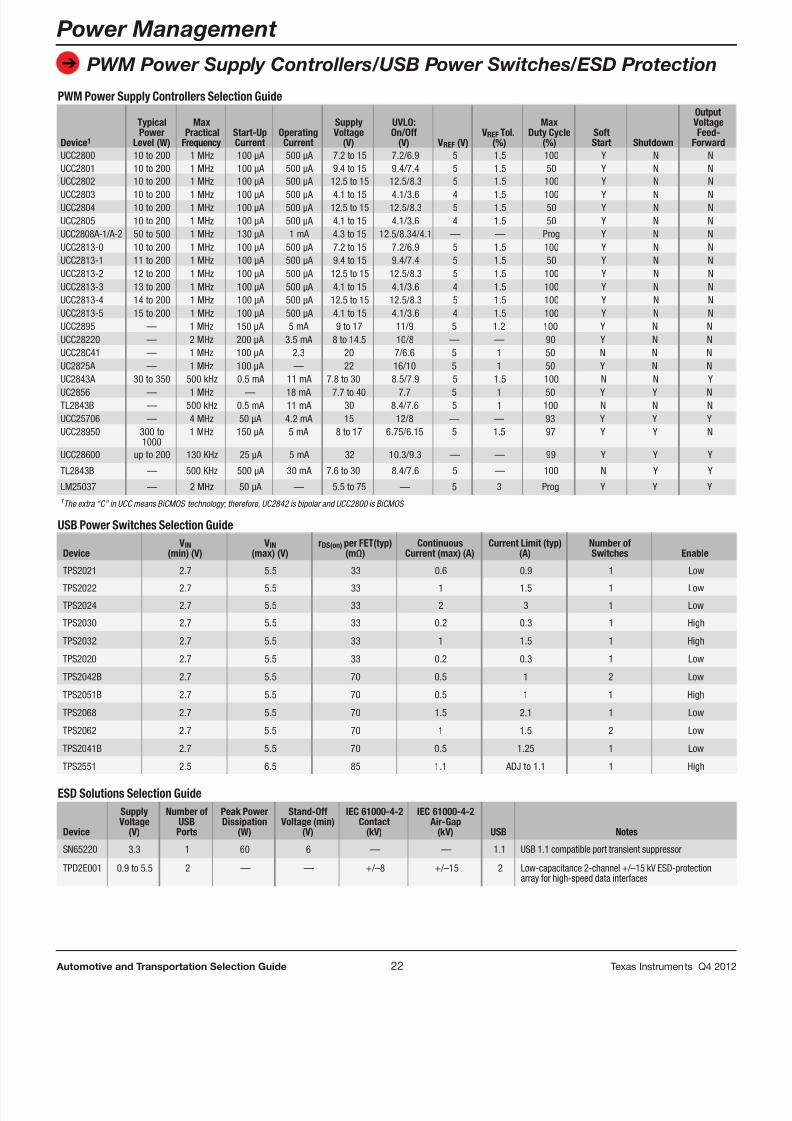
PWM Power Supply Controllers Selection Guide
Device1
TypicalPower
Level (W)
Max PracticalFrequency
Start-UpCurrent
OperatingCurrent
SupplyVoltage
(V)
UVLO:On/Off
(V) VREF (V)VREFTol.
(%)
MaxDuty Cycle
(%)SoftStart Shutdown
OutputVoltageFeed-
ForwardUCC2800 10 to 200 1 MHz 100 µA 500 µA 7.2 to 15 7.2/6.9 5 1.5 100 Y N NUCC2801 10 to 200 1 MHz 100 µA 500 µA 9.4 to 15 9.4/7.4 5 1.5 50 Y N NUCC2802 10 to 200 1 MHz 100 µA 500 µA 12.5 to 15 12.5/8.3 5 1.5 100 Y N N
UCC2803 10 to 200 1 MHz 100 µA 500 µA 4.1 to 15 4.1/3.6 4 1.5 100 Y N NUCC2804 10 to 200 1 MHz 100 µA 500 µA 12.5 to 15 12.5/8.3 5 1.5 50 Y N NUCC2805 10 to 200 1 MHz 100 µA 500 µA 4.1 to 15 4.1/3.6 4 1.5 50 Y N NUCC2808A-1/A-2 50 to 500 1 MHz 130 µA 1 mA 4.3 to 15 12.5/8.34/4.1 — — Prog Y N NUCC2813-0 10 to 200 1 MHz 100 µA 500 µA 7.2 to 15 7.2/6.9 5 1.5 100 Y N NUCC2813-1 11 to 200 1 MHz 100 µA 500 µA 9.4 to 15 9.4/7.4 5 1.5 50 Y N NUCC2813-2 12 to 200 1 MHz 100 µA 500 µA 12.5 to 15 12.5/8.3 5 1.5 100 Y N NUCC2813-3 13 to 200 1 MHz 100 µA 500 µA 4.1 to 15 4.1/3.6 4 1.5 100 Y N NUCC2813-4 14 to 200 1 MHz 100 µA 500 µA 12.5 to 15 12.5/8.3 5 1.5 100 Y N NUCC2813-5 15 to 200 1 MHz 100 µA 500 µA 4.1 to 15 4.1/3.6 4 1.5 100 Y N NUCC2895 — 1 MHz 150 µA 5 mA 9 to 17 11/9 5 1.2 100 Y N NUCC28220 — 2 MHz 200 µA 3.5 mA 8 to 14.5 10/8 — — 90 Y N NUCC28C41 — 1 MHz 100 µA 2.3 20 7/6.6 5 1 50 N N NUC2825A — 1 MHz 100 µA — 22 16/10 5 1 50 Y N NUC2843A 30 to 350 500 kHz 0.5 mA 11 mA 7.8 to 30 8.5/7.9 5 1.5 100 N N YUC2856 — 1 MHz — 18 mA 7.7 to 40 7.7 5 1 50 Y Y NTL2843B — 500 kHz 0.5 mA 11 mA 30 8.4/7.6 5 1 100 N N NUCC25706 — 4 MHz 50 µA 4.2 mA 15 12/8 — — 93 Y Y YUCC28950 300 to
10001 MHz 150 µA 5 mA 8 to 17 6.75/6.15 5 1.5 97 Y Y N
UCC28600 up to 200 130 KHz 25 µA 5 mA 32 10.3/9.3 — — 99 Y Y Y
TL2843B — 500 KHz 500 µA 30 mA 7.6 to 30 8.4/7.6 5 — 100 N Y Y
LM25037 — 2 MHz 50 µA — 5.5 to 75 — 5 3 Prog Y Y Y1The extra “C” in UCC means BiCMOS technology; therefore, UC2842 is bipolar and UCC2800 is BiCMOS
ESD Solutions Selection Guide
Device
SupplyVoltage
(V)
Number ofUSBPorts
Peak PowerDissipation
(W)
Stand-OffVoltage (min)
(V)
IEC 61000-4-2Contact
(kV)
IEC 61000-4-2Air-Gap
(kV) USB Notes
SN65220 3.3 1 60 6 — — 1.1 USB 1.1 compatible port transient suppressor
TPD2E001 0.9 to 5.5 2 — — +/–8 +/–15 2 Low-capacitance 2-channel +/–15 kV ESD-protectionarray for high-speed data interfaces
USB Power Switches Selection Guide
DeviceVIN
(min) (V)VIN
(max) (V)rDS(on) per FET(typ)
(mΩ)Continuous
Current (max) (A)Current Limit (typ)
(A)Number ofSwitches Enable
TPS2021 2.7 5.5 33 0.6 0.9 1 Low
TPS2022 2.7 5.5 33 1 1.5 1 Low
TPS2024 2.7 5.5 33 2 3 1 Low
TPS2030 2.7 5.5 33 0.2 0.3 1 High
TPS2032 2.7 5.5 33 1 1.5 1 High
TPS2020 2.7 5.5 33 0.2 0.3 1 Low
TPS2042B 2.7 5.5 70 0.5 1 2 Low
TPS2051B 2.7 5.5 70 0.5 1 1 High
TPS2068 2.7 5.5 70 1.5 2.1 1 Low
TPS2062 2.7 5.5 70 1 1.5 2 Low
TPS2041B 2.7 5.5 70 0.5 1.25 1 Low
TPS2551 2.5 6.5 85 1.1 ADJ to 1.1 1 High
8/15/2019 TI Selection Guide
http://slidepdf.com/reader/full/ti-selection-guide 23/49
➔
23 Automotive and Transportation Selection Guide Texas Instruments Q4 2012
Power Management
Supervisors/References
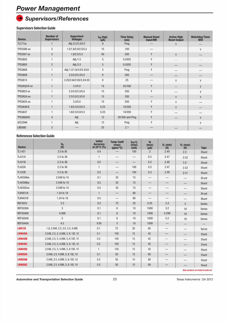
Supervisors Selection Guide
DeviceNumber of
SupervisorsSupervised
VoltagesIDO (typ)
(µA)Time Delay
(ms)Manual Reset
Input/MRActive-High
Reset OutputWatchdog Timer
WDITLC77xx 1 Adj./2.5/3.3/5.0 9 Prog — Y —
TPS3306-xx 2 1.5/1.8/2.0/2.5/3.3 15 100 — — Y
TPS3307-xx 3 1.8/2.5/3.3 40 200 Y Y —
TPS3803 1 Adj./1.5 3 0.0055 Y — —
TPS3805 2 Adj./3.3 3 0.0055 Y — —
TPS3808 1 Adj./1.2/1.8/3.0/3.3/5.0 3 Prog Y — —
TPS3809 1 2.5/3.0/3.3/5.0 9 200 — — —
TPS3813 1 2.25/2.64/2.93/3.3/4.55 9 25 — Y Y
TPS3820/8-xx 1 3.3/5.0 15 25/200 Y — Y
TPS3823-xx 1 2.5/3.0/3.3/5.0 15 200 Y — Y
TPS3824-xx 1 2.5/3.0/3.3/5.0 15 200 — Y Y
TPS3825-xx 1 3.3/5.0 15 200 Y Y —
TPS3836/8 1 1.8/2.5/3.0/3.3 0.25 10/200 Y Y —
TPS3837 1 1.8/2.5/3.0/3.3 0.25 10/200 Y — —TPS386000 4 Adj. 12 20/300 and Prog Y — Y
UCC2946 1 Adj. 12 Prog Y — Y
LM3880 3 — 25 2.1 — — —
References Selection Guide
DeviceV0(V)
InitialAccuracy
at 25°C (%)
Temp Coeff(max)
(ppm/°C)
I0UT/IZ (max)(mA)
Iq(max)(µA)
V1 (min)(V)
V1 (max)(V) Type
TL1431 2.5 to 36 0.4 — 100 2 2.49 2.51 Shunt
TL431A 2.5 to 36 1 — — 0.5 2.47 2.52 Shunt
TL431B 2.5 to 36 0.5 — — 0.5 2.48 2.51 Shunt
TL432A 2.5 to 36 1 — 100 0.5 2.47 2.52 ShuntTL432B 2.5 to 36 0.5 — 100 0.5 2.48 2.51 Shunt
TL4050Axx 2.048 to 10 0.1 50 15 — — — Shunt
TL4050Bxx 2.048 to 10 0.2 50 15 — — — Shunt
TL4050Cxx 2.048 to 10 0.5 50 15 — — — Shunt
TLVH431A 1.24 to 18 1 — 80 — — — Shunt
TLVH431B 1.24 to 18 0.5 — 80 — — — Shunt
REF3033 3.3 0.2 75 25 0.05 3.3 5 Series
REF5030A 3 0.1 8 10 1000 3.2 18 Series
REF5040A 4.096 0.1 8 10 1000 4.296 18 Series
REF5050A 5 0.1 8 10 1000 5.2 18 Series
REF5045A 4.5 0.05 3 10 1000 — — —LM4128 1.8, 2.048, 2.5, 3.0, 3.3, 4.096 0.1 75 20 60 — — Series
LM4040A 2.048, 2.5, 3, 4.096, 5, 8.192, 10 0.1 100 15 45 — — Shunt
LM4040B 2.048, 2.5, 3, 4.096, 5, 8.192, 10 0.2 100 15 45 — — Shunt
LM4040C 2.048, 2.5, 3, 4.096, 5, 8.192, 10 0.5 100 15 45 — — Shunt
LM4040D 2.048, 2.5, 3, 4.096, 5, 8.192, 10 1 150 15 45 — — Shunt
LM4050A 2.048, 2.5, 4.096, 5, 8.192, 10 0.1 50 15 60 — — Shunt
LM4050B 2.048, 2.5, 4.096, 5, 8.192, 10 0.2 50 15 60 — — Shunt
LM4050C 2.048, 2.5, 4.096, 5, 8.192, 10 0.5 50 15 60 — — Shunt
New products are listed in bold red
8/15/2019 TI Selection Guide
http://slidepdf.com/reader/full/ti-selection-guide 24/49
➔
24 Automotive and Transportation Selection Guide Texas Instruments Q4 2012
Power Management
Power and Control
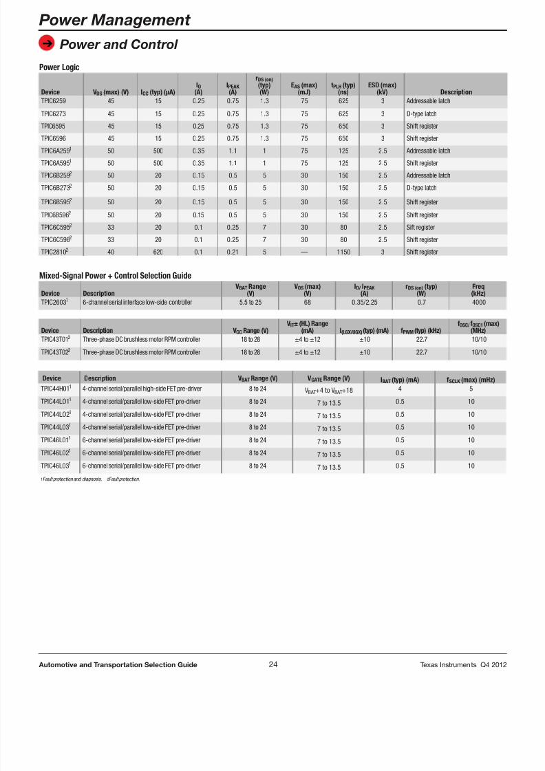
Power Logic
Device VDS (max) (V) ICC(typ) (µA)IO
(A)IPEAK (A)
rDS (on)(typ)(W)
EAS (max)(mJ)
tPLH(typ)(ns)
ESD (max)(kV) Description
TPIC6259 45 15 0.25 0.75 1.3 75 625 3 Addressable latch
TPIC6273 45 15 0.25 0.75 1.3 75 625 3 D-type latch
TPIC6595 45 15 0.25 0.75 1.3 75 650 3 Shift register
TPIC6596 45 15 0.25 0.75 1.3 75 650 3 Shift register
TPIC6A2591 50 500 0.35 1.1 1 75 125 2.5 Addressable latch
TPIC6A5951 50 500 0.35 1.1 1 75 125 2.5 Shift register
TPIC6B2592 50 20 0.15 0.5 5 30 150 2.5 Addressable latch
TPIC6B2732 50 20 0.15 0.5 5 30 150 2.5 D-type latch
TPIC6B5952 50 20 0.15 0.5 5 30 150 2.5 Shift register
TPIC6B5962 50 20 0.15 0.5 5 30 150 2.5 Shift register
TPIC6C5952 33 20 0.1 0.25 7 30 80 2.5 Sift register
TPIC6C5962 33 20 0.1 0.25 7 30 80 2.5 Shift register
TPIC28102 40 620 0.1 0.21 5 — 1150 3 Shift register
Mixed-Signal Power + Control Selection Guide
Device DescriptionVBATRange
(V)VOS (max)
(V)ID/ IPEAK
(A)rDS (on) (typ)
(W)Freq(kHz)
TPIC26031 6-channel serial interface low-side controller 5.5 to 25 68 0.35/2.25 0.7 4000
Device Description V CC Range (V)VIT± (HL) Range
(mA) I(LGX/UGX)(typ) (mA) fPWM(typ) (kHz)fOSC/fOSC1(max)
(MHz)TPIC43T012 Three-phase DC brushless motor RPM controller 18 to 28 ±4 to ±12 ±10 22.7 10/10
TPIC43T022 Three-phase DC brushless motor RPM controller 18 to 28 ±4 to ±12 ±10 22.7 10/10
Device Description V BATRange (V) VGATERange (V) IBAT(typ) (mA) fSCLK(max) (mHz)
TPIC44H011 4-channel serial/parallel high-side FET pre-driver 8 to 24 VBAT+4 to VBAT+18 4 5
TPIC44LO11 4-channel serial/parallel low-side FET pre-driver 8 to 24 7 to 13.5 0.5 10
TPIC44LO21 4-channel serial/parallel low-side FET pre-driver 8 to 24 7 to 13.5 0.5 10
TPIC44L031 4-channel serial/parallel low-side FET pre-driver 8 to 24 7 to 13.5 0.5 10
TPIC46L011 6-channel serial/parallel low-side FET pre-driver 8 to 24 7 to 13.5 0.5 10
TPIC46L021 6-channel serial/parallel low-side FET pre-driver 8 to 24 7 to 13.5 0.5 10
TPIC46L031 6-channel serial/parallel low-side FET pre-driver 8 to 24 7 to 13.5 0.5 10
1Fault protection and diagnosis. 2Fault protection.
8/15/2019 TI Selection Guide
http://slidepdf.com/reader/full/ti-selection-guide 25/49
➔
25 Automotive and Transportation Selection Guide Texas Instruments Q4 2012
Power Management
Power and Control
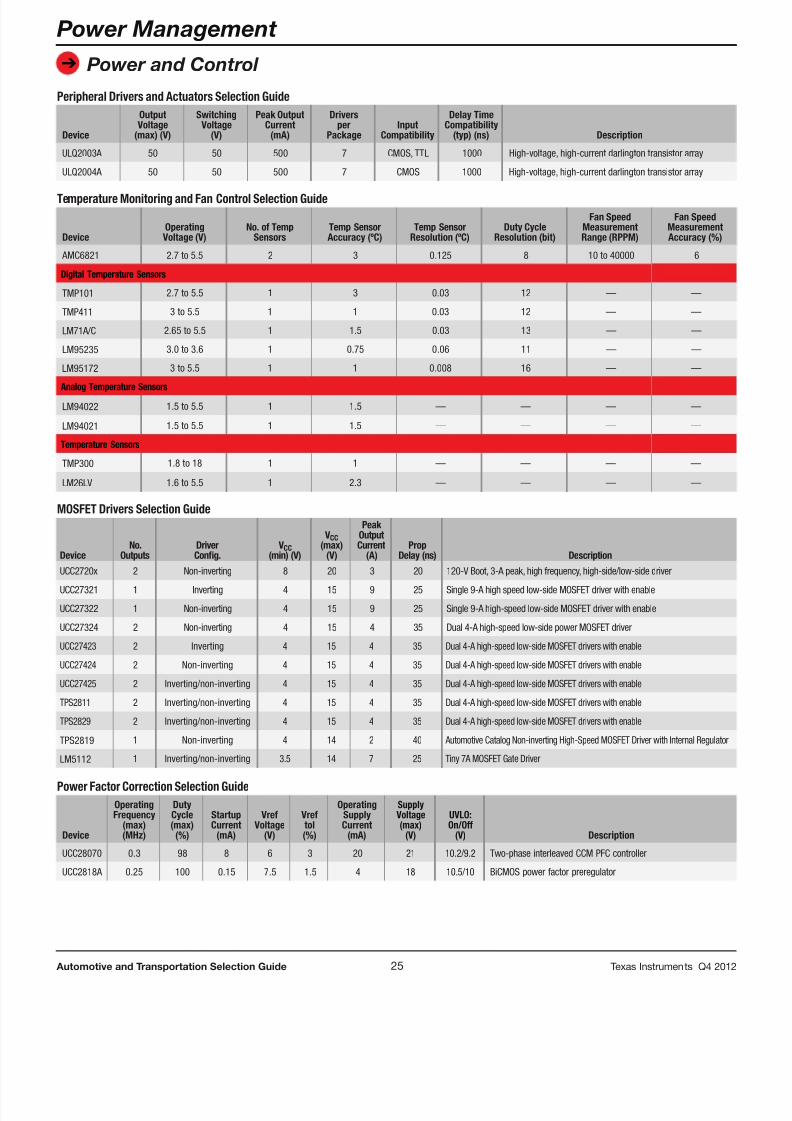
Peripheral Drivers and Actuators Selection Guide
Device
OutputVoltage
(max) (V)
SwitchingVoltage
(V)
Peak OutputCurrent
(mA)
Driversper
PackageInput
Compatibility
Delay TimeCompatibility
(typ) (ns) Description
ULQ2003A 50 50 500 7 CMOS, TTL 1000 High-voltage, high-current darlington transistor array
ULQ2004A 50 50 500 7 CMOS 1000 High-voltage, high-current darlington transistor array
Power Factor Correction Selection Guide
Device
OperatingFrequency
(max)(MHz)
DutyCycle(max)
(%)
StartupCurrent
(mA)
VrefVoltage
(V)
Vreftol(%)
OperatingSupplyCurrent
(mA)
SupplyVoltage(max)
(V)
UVLO:On/Off
(V) Description
UCC28070 0.3 98 8 6 3 20 21 10.2/9.2 Two-phase interleaved CCM PFC controller
UCC2818A 0.25 100 0.15 7.5 1.5 4 18 10.5/10 BiCMOS power factor preregulator
Temperature Monitoring and Fan Control Selection Guide
DeviceOperatingVoltage (V)
No. of TempSensors
Temp SensorAccuracy (ºC)
Temp SensorResolution (ºC)
Duty CycleResolution (bit)
Fan SpeedMeasurementRange (RPPM)
Fan SpeedMeasurementAccuracy (%)
AMC6821 2.7 to 5.5 2 3 0.125 8 10 to 40000 6
Digital Temperature Sensors
TMP101 2.7 to 5.5 1 3 0.03 12 — —
TMP411 3 to 5.5 1 1 0.03 12 — —
LM71A/C 2.65 to 5.5 1 1.5 0.03 13 — —
LM95235 3.0 to 3.6 1 0.75 0.06 11 — —
LM95172 3 to 5.5 1 1 0.008 16 — —
Analog Temperature SensorsLM94022 1.5 to 5.5 1 1.5 — — — —
LM94021 1.5 to 5.5 1 1.5 — — — —
Temperature Sensors
TMP300 1.8 to 18 1 1 — — — —
LM26LV 1.6 to 5.5 1 2.3 — — — —
MOSFET Drivers Selection Guide
DeviceNo.
OutputsDriverCong.
VCC(min) (V)
VCC(max)
(V)
PeakOutputCurrent
(A)Prop
Delay (ns) Description
UCC2720x 2 Non-inverting 8 20 3 20 120-V Boot, 3-A peak, high frequency, high-side/low-side driver
UCC27321 1 Inverting 4 15 9 25 Single 9-A high speed low-side MOSFET driver with enable
UCC27322 1 Non-inverting 4 15 9 25 Single 9-A high-speed low-side MOSFET driver with enable
UCC27324 2 Non-inverting 4 15 4 35 Dual 4-A high-speed low-side power MOSFET driver
UCC27423 2 Inverting 4 15 4 35 Dual 4-A high-speed low-side MOSFET drivers with enable
UCC27424 2 Non-inverting 4 15 4 35 Dual 4-A high-speed low-side MOSFET drivers with enable
UCC27425 2 Inverting/non-inverting 4 15 4 35 Dual 4-A high-speed low-side MOSFET drivers with enable
TPS2811 2 Inverting/non-inverting 4 15 4 35 Dual 4-A high-speed low-side MOSFET drivers with enable
TPS2829 2 Inverting/non-inverting 4 15 4 35 Dual 4-A high-speed low-side MOSFET drivers with enable
TPS2819 1 Non-inverting 4 14 2 40 Automotive Catalog Non-inverting High-Speed MOSFET Driver with Internal Reg
LM5112 1 Inverting/non-inverting 3.5 14 7 25 Tiny 7A MOSFET Gate Driver
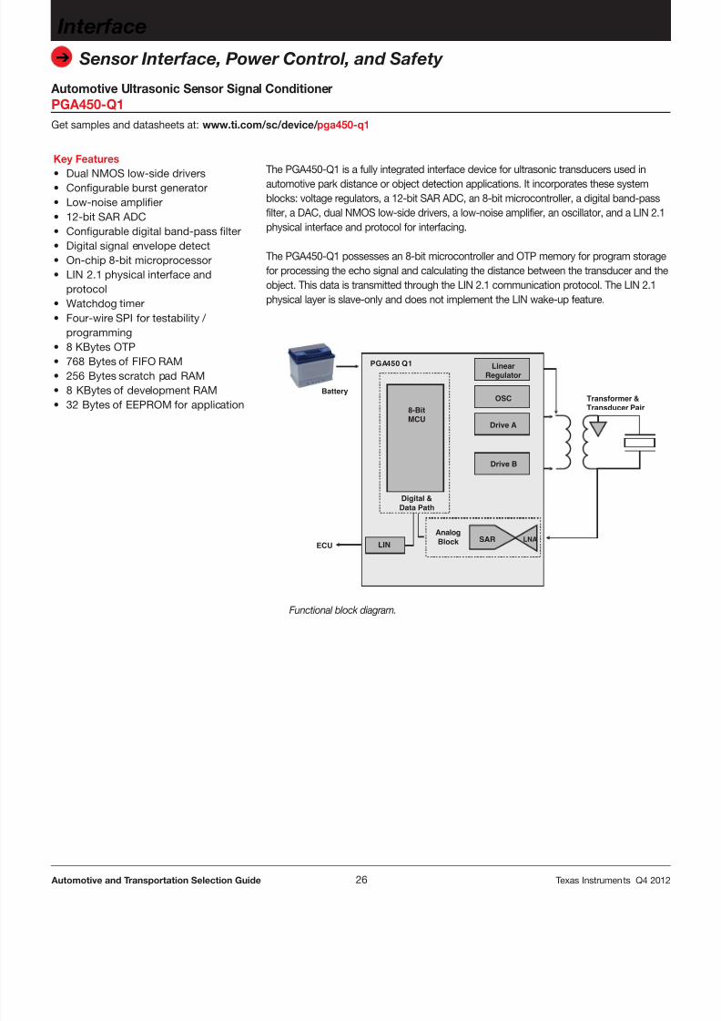
8/15/2019 TI Selection Guide
http://slidepdf.com/reader/full/ti-selection-guide 26/49
26 Automotive and Transportation Selection Guide Texas Instruments Q4 2012
➔
Interface
Sensor Interface, Power Control, and Safety
Automotive Ultrasonic Sensor Signal ConditionerPGA450-Q1Get samples and datasheets at: www.ti.com/sc/device/ pga450-q1
Key Features
• Dual NMOS low-side drivers• Configurable burst generator• Low-noise amplifier• 12-bit SAR ADC• Configurable digital band-pass filter• Digital signal envelope detect• On-chip 8-bit microprocessor• LIN 2.1 physical interface and
protocol• Watchdog timer• Four-wire SPI for testability /
programming• 8 KBytes OTP• 768 Bytes of FIFO RAM• 256 Bytes scratch pad RAM• 8 KBytes of development RAM• 32 Bytes of EEPROM for application
The PGA450-Q1 is a fully integrated interface device for ultrasonic transducers used inautomotive park distance or object detection applications. It incorporates these systemblocks: voltage regulators, a 12-bit SAR ADC, an 8-bit microcontroller, a digital band-passfilter, a DAC, dual NMOS low-side drivers, a low-noise amplifier, an oscillator, and a LIN 2.1physical interface and protocol for interfacing.
The PGA450-Q1 possesses an 8-bit microcontroller and OTP memory for program storagefor processing the echo signal and calculating the distance between the transducer and theobject. This data is transmitted through the LIN 2.1 communication protocol. The LIN 2.1physical layer is slave-only and does not implement the LIN wake-up feature.
Battery
ECU LIN
PGA450 Q1
8-BitMCU
Digital &Data Path
AnalogBlock SAR LNA
OSC
LinearRegulator
Drive A
Drive B
Transformer &Transducer Pair
Functional block diagram.
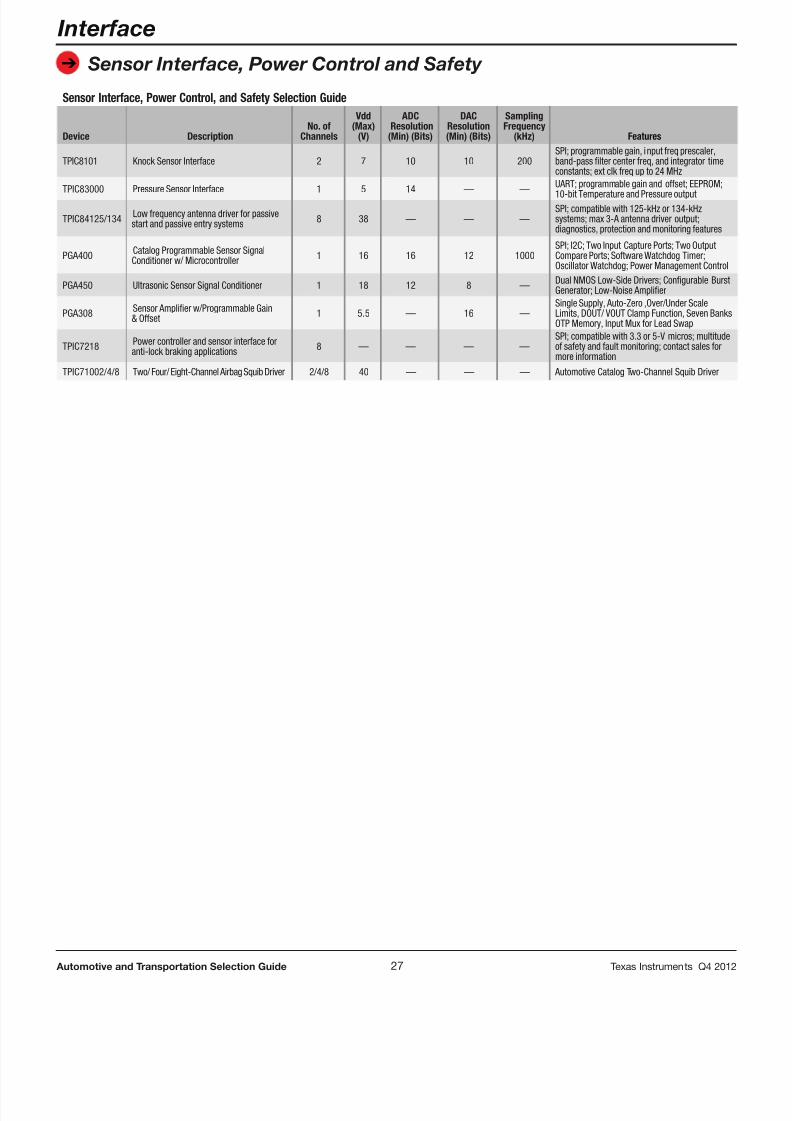
8/15/2019 TI Selection Guide
http://slidepdf.com/reader/full/ti-selection-guide 27/49
➔
27 Automotive and Transportation Selection Guide Texas Instruments Q4 2012
Interface
Sensor Interface, Power Control and Safety
Sensor Interface, Power Control, and Safety Selection Guide
Device DescriptionNo. of
Channels
Vdd(Max)
(V)
ADC Resolution(Min) (Bits)
DACResolution(Min) (Bits)
SamplingFrequency
(kHz) Features
TPIC8101 Knock Sensor Interface 2 7 10 10 200SPI; programmable gain, input freq prescaler,band-pass lter center freq, and integrator timeconstants; ext clk freq up to 24 MHz
TPIC83000 Pressure Sensor Interface 1 5 14 — —UART; programmable gain and offset; EEPROM10-bit Temperature and Pressure output
TPIC84125/134 Low frequency antenna driver for passivestart and passive entry systems 8 38 — — —
SPI; compatible with 125-kHz or 134-kHzsystems; max 3-A antenna driver output;diagnostics, protection and monitoring features
PGA400 Catalog Programmable Sensor SignalConditioner w/ Microcontroller 1 16 16 12 1000
SPI; I2C; Two Input Capture Ports; Two OutputCompare Ports; Software Watchdog Timer;Oscillator Watchdog; Power Management Contro
PGA450 Ultrasonic Sensor Signal Conditioner 1 18 12 8 — Dual NMOS Low-Side Drivers; Congurable BuGenerator; Low-Noise Amplier
PGA308 Sensor Amplier w/Programmable Gain& Offset 1 5.5 — 16 —
Single Supply, Auto-Zero ,Over/Under ScaleLimits, DOUT/ VOUT Clamp Function, Seven BOTP Memory, Input Mux for Lead Swap
TPIC7218 Power controller and sensor interface foranti-lock braking applications 8 — — — —
SPI; compatible with 3.3 or 5-V micros; multitudof safety and fault monitoring; contact sales formore information
TPIC71002/4/8 Two/ Four/ Eight-Channel Airbag Squib Driver 2/4/8 40 — — — Automotive Catalog Two-Channel Squib Driver
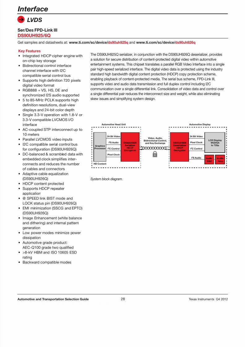
8/15/2019 TI Selection Guide
http://slidepdf.com/reader/full/ti-selection-guide 28/49
➔
28 Automotive and Transportation Selection Guide Texas Instruments Q4 2012
Interface
LVDS
Ser/Des FPD-Link IIIDS90UH925/6QGet samples and datasheets at: www.ti.com/sc/device/ ds90uh925q and www.ti.com/sc/device/ ds90uh926q
Key Features• Integrated HDCP cipher engine with
on-chip key storage• Bidirectional control interface
channel interface with I2Ccompatible serial control bus
• Supports high definition 720 pixelsdigital video format
• RGB888 + VS, HS, DE andsynchronized I2S audio supported
• 5 to 85-MHz PCLK supports highdefinition resolutions, dual-viewdisplays and 24-bit color depth
• Single 3.3-V operation with 1.8-V or
3.3-V compatible LVCMOS I/Ointerface
• AC-coupled STP interconnect up to10 meters
• Parallel LVCMOS video inputs• I2C compatible serial control bus
for configuration (DS90UH926Q)• DC-balanced & scrambled data with
embedded clock simplifies inter-connects and reduces the numberof cables and connectors
• Adaptive cable equalization
(DS90UH926Q)• HDCP content protected• Supports HDCP repeater
application• @ SPEED link BIST mode and
LOCK status pin (DS90UH926Q)• EMI minimization (SSCG and EPTO)
(DS90UH926Q)• Image Enhancement (white balance
and dithering) and internal patterngeneration
• Low power modes minimize powerdissipation
• Automotive grade product: AEC-Q100 grade two qualified
• >8-kV HBM and ISO 10605 ESDrating
• Backward compatible modes
The DS90UH925Q serializer, in conjunction with the DS90UH926Q deserializer, provides
a solution for secure distribution of content-protected digital video within automotiveentertainment systems. This chipset translates a parallel RGB Video Interface into a singlepair high-speed serialized interface. The digital video data is protected using the industrystandard high bandwidth digital content protection (HDCP) copy protection scheme,enabling playback of content-protected media. The serial bus scheme, FPD-Link III,supports video and audio data transmission and full duplex control including I2Ccommunication over a single differential link. Consolidation of video data and control overa single differential pair reduces the interconnect size and weight, while also eliminatingskew issues and simplifying system design.
System block diagram.
Automotive Head Unit Automotive Display
24 Bit Video
I2S Audio
I2C Control
Pixel Clock
24 Bit Video
I2S Audio AudioDAC
Audio Amp
I2C Control
Pixel Clock
GraphicsProcessor
LCD Display WQVGA to 720p
Video, Audio,Bidirectional Control,
and Key Exchange
HD Content
DS90UH925Serializer
HDCPEncryption
DS90UH926Deserializer
HDCPDecryption
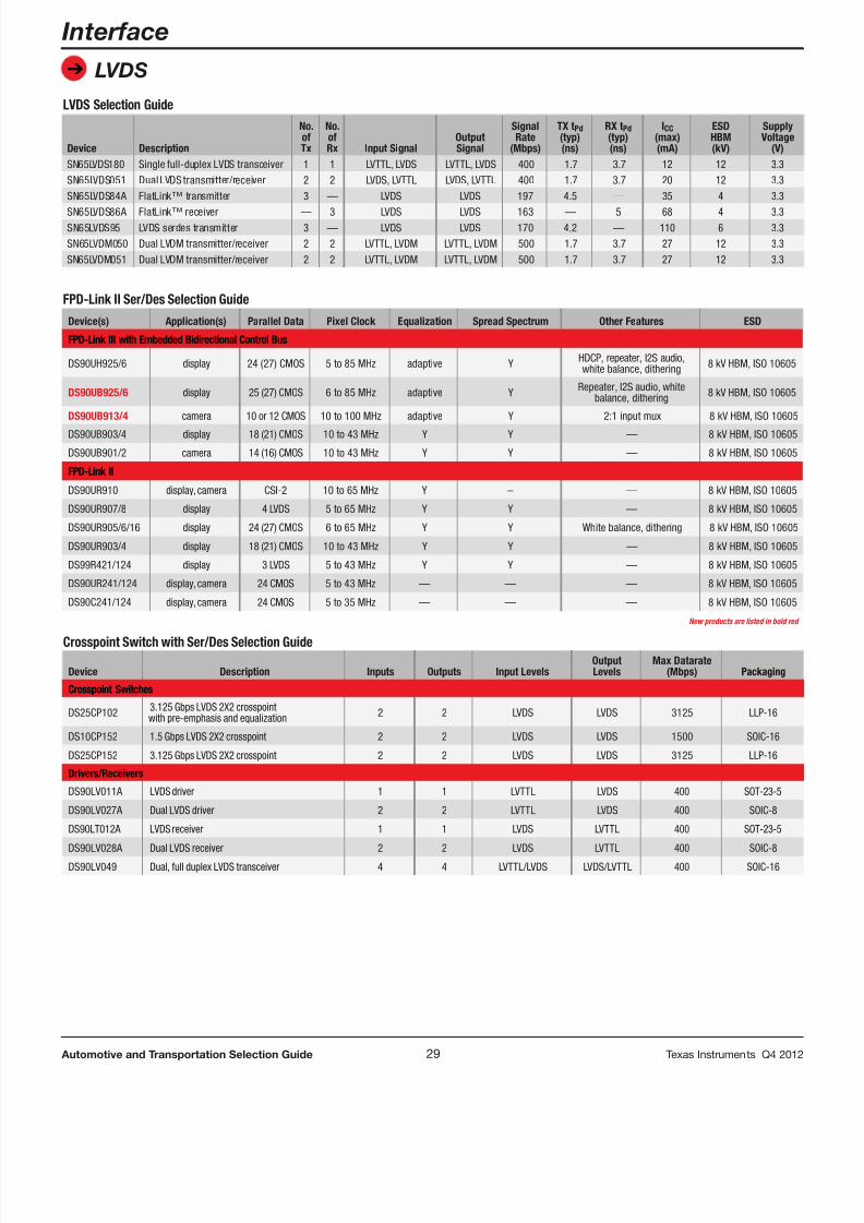
8/15/2019 TI Selection Guide
http://slidepdf.com/reader/full/ti-selection-guide 29/49
➔
29 Automotive and Transportation Selection Guide Texas Instruments Q4 2012
Interface
LVDS
FPD-Link II Ser/Des Selection Guide
Device(s) Application(s) Parallel Data Pixel Clock Equalization Spread Spectrum Other Features ESD
FPD-Link III with Embedded Bidirectional Control Bus
DS90UH925/6 display 24 (27) CMOS 5 to 85 MHz adaptive Y HDCP, repeater, I2S audio,white balance, dithering 8 kV HBM, ISO 10605
DS90UB925/6 display 25 (27) CMOS 6 to 85 MHz adaptive Y Repeater, I2S audio, whitebalance, dithering 8 kV HBM, ISO 10605
DS90UB913/4 camera 10 or 12 CMOS 10 to 100 MHz adaptive Y 2:1 input mux 8 kV HBM, ISO 1060
DS90UB903/4 display 18 (21) CMOS 10 to 43 MHz Y Y — 8 kV HBM, ISO 1060
DS90UB901/2 camera 14 (16) CMOS 10 to 43 MHz Y Y — 8 kV HBM, ISO 1060
FPD-Link II
DS90UR910 display, camera CSI-2 10 to 65 MHz Y – — 8 kV HBM, ISO 10605
DS90UR907/8 display 4 LVDS 5 to 65 MHz Y Y — 8 kV HBM, ISO 1060
DS90UR905/6/16 display 24 (27) CMOS 6 to 65 MHz Y Y White balance, dithering 8 kV HBM, ISO 106
DS90UR903/4 display 18 (21) CMOS 10 to 43 MHz Y Y — 8 kV HBM, ISO 1060
DS99R421/124 display 3 LVDS 5 to 43 MHz Y Y — 8 kV HBM, ISO 1060
DS90UR241/124 display, camera 24 CMOS 5 to 43 MHz — — — 8 kV HBM, ISO 10605
DS90C241/124 display, camera 24 CMOS 5 to 35 MHz — — — 8 kV HBM, ISO 10605
New products are listed in bold red
LVDS Selection Guide
Device Description
No.ofTx
No.ofRx Input Signal
OutputSignal
SignalRate
(Mbps)
TX tPd(typ)(ns)
RX tPd(typ)(ns)
ICC(max)(mA)
ESDHBM(kV)
SupplyVoltage
(V)SN65LVDS180 Single full-duplex LVDS transceiver 1 1 LVTTL, LVDS LVTTL, LVDS 400 1.7 3.7 12 12 3.3SN65LVDS051 Dual LVDS transmitter/receiver 2 2 LVDS, LVTTL LVDS, LVTTL 400 1.7 3.7 20 12 3.3SN65LVDS84A FlatLink™ transmitter 3 — LVDS LVDS 197 4.5 — 35 4 3.3
SN65LVDS86A FlatLink™ receiver — 3 LVDS LVDS 163 — 5 68 4 3.3SN65LVDS95 LVDS serdes transmitter 3 — LVDS LVDS 170 4.2 — 110 6 3.3SN65LVDM050 Dual LVDM transmitter/receiver 2 2 LVTTL, LVDM LVTTL, LVDM 500 1.7 3.7 27 12 3.3SN65LVDM051 Dual LVDM transmitter/receiver 2 2 LVTTL, LVDM LVTTL, LVDM 500 1.7 3.7 27 12 3.3
Crosspoint Switch with Ser/Des Selection Guide
Device Description Inputs Outputs Input LevelsOutputLevels
Max Datarate(Mbps) Packaging
Crosspoint Switches
DS25CP102 3.125 Gbps LVDS 2X2 crosspointwith pre-emphasis and equalization 2 2 LVDS LVDS 3125 LLP-16
DS10CP152 1.5 Gbps LVDS 2X2 crosspoint 2 2 LVDS LVDS 1500 SOIC-16
DS25CP152 3.125 Gbps LVDS 2X2 crosspoint 2 2 LVDS LVDS 3125 LLP-16
Drivers/Receivers
DS90LV011A LVDS driver 1 1 LVTTL LVDS 400 SOT-23-5
DS90LV027A Dual LVDS driver 2 2 LVTTL LVDS 400 SOIC-8
DS90LT012A LVDS receiver 1 1 LVDS LVTTL 400 SOT-23-5
DS90LV028A Dual LVDS receiver 2 2 LVDS LVTTL 400 SOIC-8DS90LV049 Dual, full duplex LVDS transceiver 4 4 LVTTL/LVDS LVDS/LVTTL 400 SOIC-16
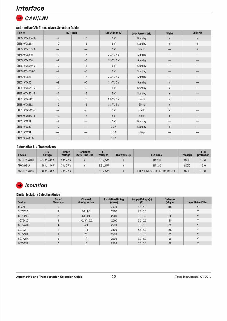
8/15/2019 TI Selection Guide
http://slidepdf.com/reader/full/ti-selection-guide 30/49
➔
30 Automotive and Transportation Selection Guide Texas Instruments Q4 2012
Interface
CAN/LIN
Digital Isolators Selection Guide
DeviceNo. of
ChannelsChannel
CongurationInsulation Rating
(Vrms)Supply Voltage(s)
(V)Datarate(Mbps) Input Noise Filter
ISO721 1 2500 3.3, 5.0 100 Y
ISO722xA 2 2/0, 1/1 2500 3.3, 5.0 1 Y
ISO722xC 2 2/0, 1/1 2500 3.3, 5.0 25 Y
ISO724xC 4 4/0, 3/1, 2/2 2500 3.3, 5.0 25 Y
ISO7240CF 4 4/0 2500 3.3, 5.0 25 Y
ISO722 1 1/0 2500 3.3, 5.0 100 Y
ISO7231C 3 2/1 2500 3.3, 5.0 25 Y
ISO7421A 2 1/1 2500 3.3, 5.0 50 Y
ISO7421E 2 1/1 2500 3.3, 5.0 50 Y
Isolation➔
Automotive CAN Transceivers Selection GuideDevice ISO11898 I/O Voltage (V) Low Power State Wake Split Pin
SN65HVDA1040A –2 –5 5 V Standby Y Y
SN65HVDA553 –2 –5 5 V Standby Y Y
SN65HVDA1050A –2 — 5 V Silent — Y
SN65HVDA540 –2 –5 3.3 V / 5 V Standby — —SN65HVDA550 –2 –5 3.3 V / 5 V Standby — —
SN65HVDA540-5 –2 –5 5 V Standby — —
SN65HCDA550-5 –2 –5 5 V Standby — —
SN65HVDA541 –2 –5 3.3 V / 5 V Standby — —
SN65HVDA551 –2 –5 3.3 V / 5 V Standby Y —
SN65HVDA541-5 –2 –5 5 V Standby Y —
SN65HVDA551-5 –2 –5 5 V Standby Y —
SN65HVDA542 –2 –5 3.3 V / 5 V Silent Y —
SN65HVDA552 –2 –5 3.3 V / 5 V Silent Y —
SN65HVDA542-5 –2 –5 5 V Silent Y —SN65HVDA552-5 –2 –5 5 V Silent Y —
SN65HVD251 –2 — 5 V Standby — —
SN65HVD230 –2 — 3.3 V Standby Y —
SN65HVD231 –2 — 3.3 V Sleep — —
SN65HVD232-5 –2 — 3.3 V — —
Automotive LIN Transceivers
DeviceLIN
VoltageSupplyVoltage
DominantState Time Out
IOVoltages Bus Wake-up Bus Spec Package
ESDprotection
SN65HVDA100 –27 to +45 V 5 to 27 V Y 3.3 V, 5 V Y LIN 2.0 8SOIC 12 kV
TPIC1021A –40 to +40 V 7 to 27 V Y 3.3 V, 5 V Y LIN 2.0 8SOIC 12 kVSN65HVDA195 –40 to +40 V 7 to 27 V — 3.3 V, 5 V Y LIN 2.1, MOST ECL, K-Line, ISO9141 8SOIC 12 kV
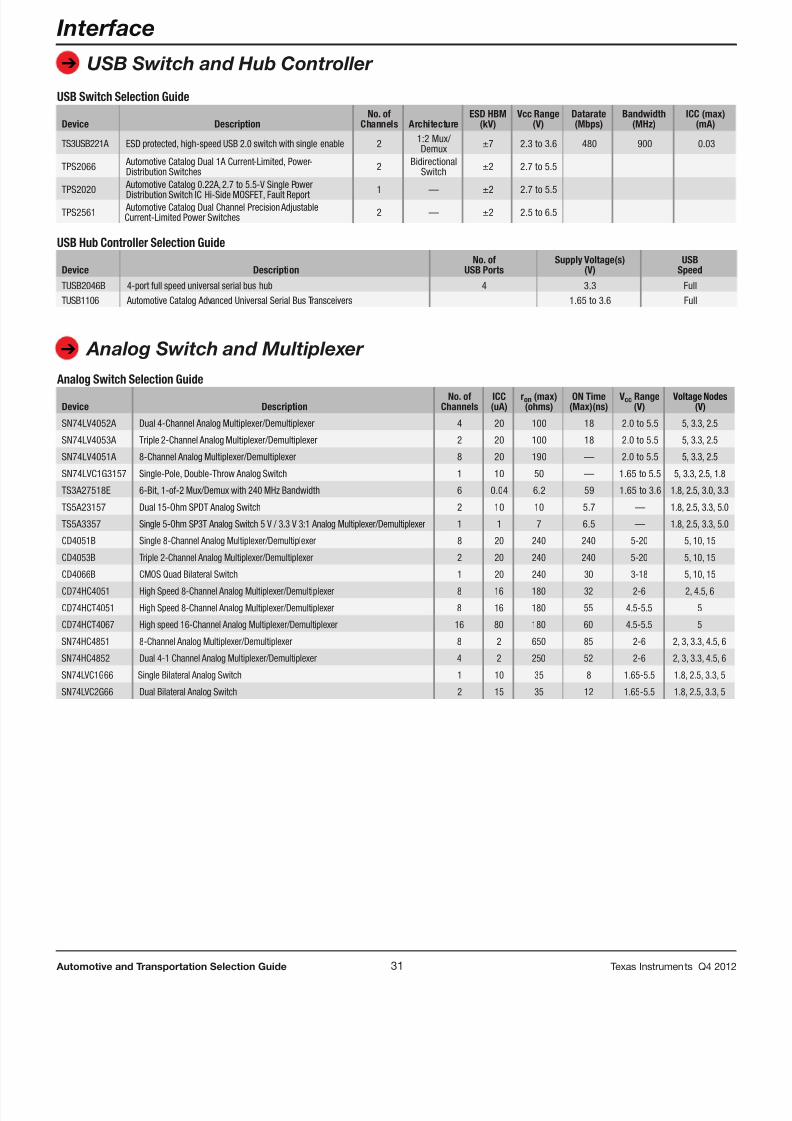
8/15/2019 TI Selection Guide
http://slidepdf.com/reader/full/ti-selection-guide 31/49
➔
31 Automotive and Transportation Selection Guide Texas Instruments Q4 2012
Interface
USB Switch and Hub Controller
Analog Switch Selection Guide
Device DescriptionNo. of
ChannelsICC(uA)
ron (max)(ohms)
ON Time(Max)(ns)
Vcc Range(V)
Voltage Nodes(V)
SN74LV4052A Dual 4-Channel Analog Multiplexer/Demultiplexer 4 20 100 18 2.0 to 5.5 5, 3.3, 2.5
SN74LV4053A Triple 2-Channel Analog Multiplexer/Demultiplexer 2 20 100 18 2.0 to 5.5 5, 3.3, 2.5
SN74LV4051A 8-Channel Analog Multiplexer/Demultiplexer 8 20 190 — 2.0 to 5.5 5, 3.3, 2.5
SN74LVC1G3157 Single-Pole, Double-Throw Analog Switch 1 10 50 — 1.65 to 5.5 5, 3.3, 2.5, 1.8
TS3A27518E 6-Bit, 1-of-2 Mux/Demux with 240 MHz Bandwidth 6 0.04 6.2 59 1.65 to 3.6 1.8, 2.5, 3.0, 3.3
TS5A23157 Dual 15-Ohm SPDT Analog Switch 2 10 10 5.7 — 1.8, 2.5, 3.3, 5.0
TS5A3357 Single 5-Ohm SP3T Analog Switch 5 V / 3.3 V 3:1 Analog Multiplexer/Demultiplexer 1 1 7 6.5 — 1.8, 2.5, 3.3, 5.0
CD4051B Single 8-Channel Analog Multiplexer/Demultiplexer 8 20 240 240 5-20 5, 10, 15
CD4053B Triple 2-Channel Analog Multiplexer/Demultiplexer 2 20 240 240 5-20 5, 10, 15
CD4066B CMOS Quad Bilateral Switch 1 20 240 30 3-18 5, 10, 15
CD74HC4051 High Speed 8-Channel Analog Multiplexer/Demultiplexer 8 16 180 32 2-6 2, 4.5, 6
CD74HCT4051 High Speed 8-Channel Analog Multiplexer/Demultiplexer 8 16 180 55 4.5-5.5 5
CD74HCT4067 High speed 16-Channel Analog Multiplexer/Demultiplexer 16 80 180 60 4.5-5.5 5
SN74HC4851 8-Channel Analog Multiplexer/Demultiplexer 8 2 650 85 2-6 2, 3, 3.3, 4.5,
SN74HC4852 Dual 4-1 Channel Analog Multiplexer/Demultiplexer 4 2 250 52 2-6 2, 3, 3.3, 4.5
SN74LVC1G66 Single Bilateral Analog Switch 1 10 35 8 1.65-5.5 1.8, 2.5, 3.3,
SN74LVC2G66 Dual Bilateral Analog Switch 2 15 35 12 1.65-5.5 1.8, 2.5, 3.3,
USB Hub Controller Selection Guide
Device DescriptionNo. of
USB PortsSupply Voltage(s)
(V)USB
Speed
TUSB2046B 4-port full speed universal serial bus hub 4 3.3 FullTUSB1106 Automotive Catalog Advanced Universal Serial Bus Transceivers 1.65 to 3.6 Full
Analog Switch and Multiplexer ➔
USB Switch Selection Guide
Device DescriptionNo. of
Channels ArchitectureESD HBM
(kV)Vcc Range
(V)Datarate(Mbps)
Bandwidth(MHz)
ICC (max)(mA)
TS3USB221A ESD protected, high-speed USB 2.0 switch with single enable 2 1:2 Mux/ Demux ±7 2.3 to 3.6 480 900 0.03
TPS2066 Automotive Catalog Dual 1A Current-Limited, Power-Distribution Switches 2 Bidirectional
Switch ±2 2.7 to 5.5
TPS2020 Automotive Catalog 0.22A, 2.7 to 5.5-V Single PowerDistribution Switch IC Hi-Side MOSFET, Fault Report 1 — ±2 2.7 to 5.5
TPS2561 Automotive Catalog Dual Channel Precision AdjustableCurrent-Limited Power Switches 2 — ±2 2.5 to 6.5
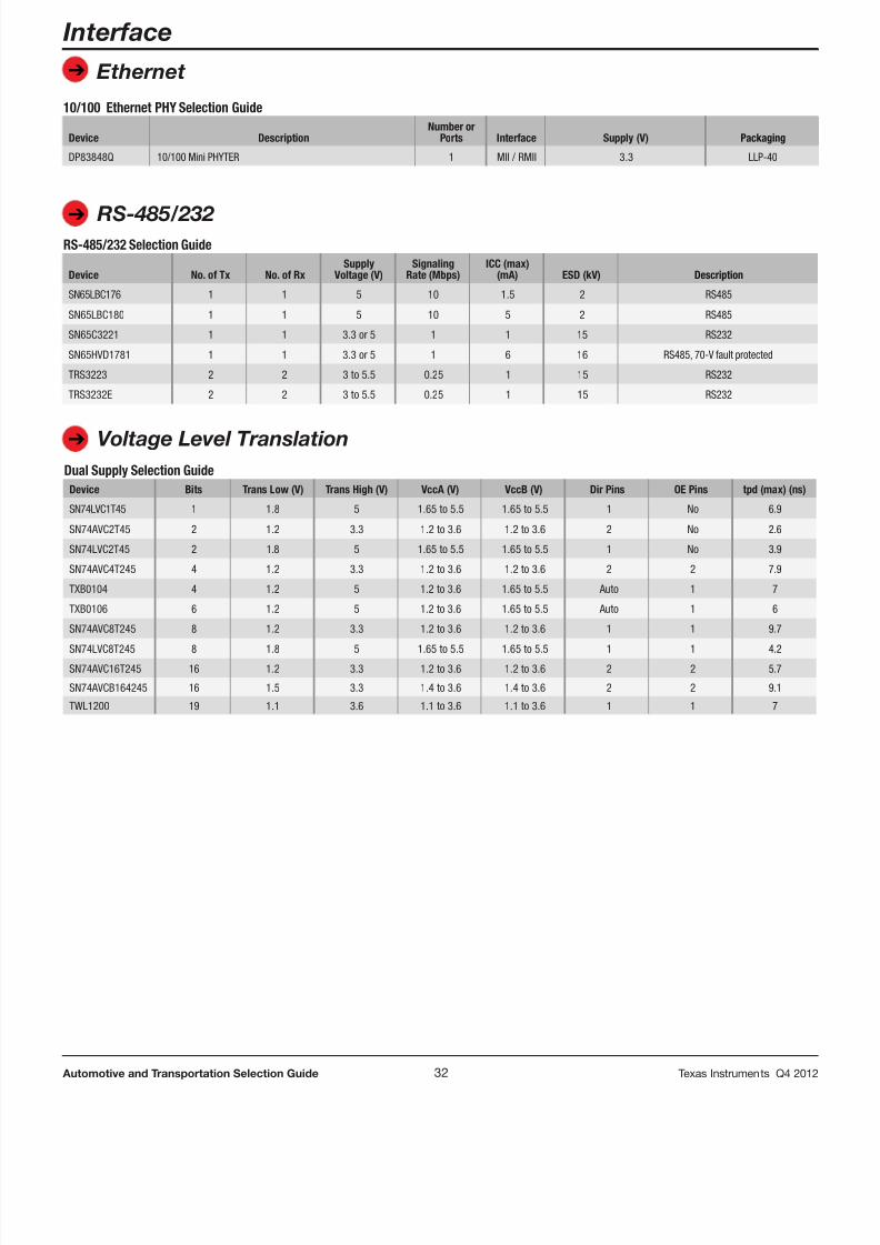
8/15/2019 TI Selection Guide
http://slidepdf.com/reader/full/ti-selection-guide 32/49
➔
32 Automotive and Transportation Selection Guide Texas Instruments Q4 2012
Interface
Ethernet
Dual Supply Selection GuideDevice Bits Trans Low (V) Trans High (V) VccA (V) VccB (V) Dir Pins OE Pins tpd (max) (ns)
SN74LVC1T45 1 1.8 5 1.65 to 5.5 1.65 to 5.5 1 No 6.9
SN74AVC2T45 2 1.2 3.3 1.2 to 3.6 1.2 to 3.6 2 No 2.6
SN74LVC2T45 2 1.8 5 1.65 to 5.5 1.65 to 5.5 1 No 3.9
SN74AVC4T245 4 1.2 3.3 1.2 to 3.6 1.2 to 3.6 2 2 7.9
TXB0104 4 1.2 5 1.2 to 3.6 1.65 to 5.5 Auto 1 7
TXB0106 6 1.2 5 1.2 to 3.6 1.65 to 5.5 Auto 1 6
SN74AVC8T245 8 1.2 3.3 1.2 to 3.6 1.2 to 3.6 1 1 9.7
SN74LVC8T245 8 1.8 5 1.65 to 5.5 1.65 to 5.5 1 1 4.2
SN74AVC16T245 16 1.2 3.3 1.2 to 3.6 1.2 to 3.6 2 2 5.7
SN74AVCB164245 16 1.5 3.3 1.4 to 3.6 1.4 to 3.6 2 2 9.1
TWL1200 19 1.1 3.6 1.1 to 3.6 1.1 to 3.6 1 1 7
RS-485/232 Selection Guide
Device No. of Tx No. of RxSupply
Voltage (V)Signaling
Rate (Mbps)ICC (max)
(mA) ESD (kV) Description
SN65LBC176 1 1 5 10 1.5 2 RS485
SN65LBC180 1 1 5 10 5 2 RS485
SN65C3221 1 1 3.3 or 5 1 1 15 RS232
SN65HVD1781 1 1 3.3 or 5 1 6 16 RS485, 70-V fault protected
TRS3223 2 2 3 to 5.5 0.25 1 15 RS232
TRS3232E 2 2 3 to 5.5 0.25 1 15 RS232
10/100 Ethernet PHY Selection Guide
Device DescriptionNumber or
Ports Interface Supply (V) Packaging
DP83848Q 10/100 Mini PHYTER 1 MII / RMII 3.3 LLP-40
RS-485/232
Voltage Level Translation
➔
➔
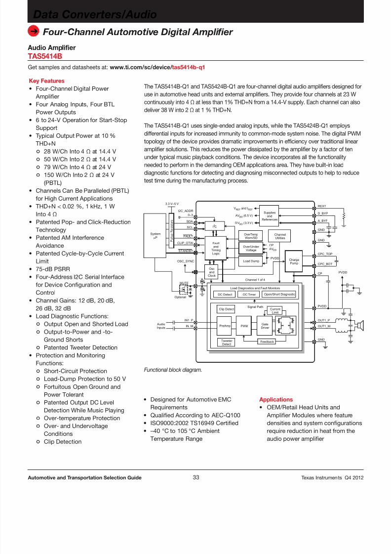
8/15/2019 TI Selection Guide
http://slidepdf.com/reader/full/ti-selection-guide 33/49
33 Automotive and Transportation Selection Guide Texas Instruments Q4 2012
➔
Data Converters/Audio
Four-Channel Automotive Digital Amplifier
Audio AmplifierTAS5414BGet samples and datasheets at: www.ti.com/sc/device/ tas5414b-q1
Key Features• Four-Channel Digital Power
Amplifier• Four Analog Inputs, Four BTL
Power Outputs• 6 to 24-V Operation for Start-Stop
Support• Typical Output Power at 10 %
THD+N ° 28 W/Ch Into 4 Ω at 14.4 V ° 50 W/Ch Into 2 Ω at 14.4 V ° 79 W/Ch Into 4 Ω at 24 V ° 150 W/Ch Into 2 Ω at 24 V
(PBTL)
• Channels Can Be Paralleled (PBTL)for High Current Applications
• THD+N < 0.02 %, 1 kHz, 1 WInto 4 Ω
• Patented Pop- and Click-ReductionTechnology
• Patented AM Interference Avoidance
• Patented Cycle-by-Cycle CurrentLimit
• 75-dB PSRR• Four-Address I2C Serial Interface
for Device Configuration andControl• Channel Gains: 12 dB, 20 dB,
26 dB, 32 dB• Load Diagnostic Functions: ° Output Open and Shorted Load ° Output-to-Power and -to-
Ground Shorts ° Patented Tweeter Detection• Protection and Monitoring
Functions: ° Short-Circuit Protection
° Load-Dump Protection to 50 V
° Fortuitous Open Ground andPower Tolerant
° Patented Output DC LevelDetection While Music Playing
° Over-temperature Protection ° Over- and Undervoltage
Conditions ° Clip Detection
The TAS5414B-Q1 and TAS5424B-Q1 are four-channel digital audio amplifiers designed for
use in automotive head units and external amplifiers. They provide four channels at 23 Wcontinuously into 4 Ω at less than 1% THD+N from a 14.4-V supply. Each channel can alsodeliver 38 W into 2 Ω at 1 % THD+N.
The TAS5414B-Q1 uses single-ended analog inputs, while the TAS5424B-Q1 employsdifferential inputs for increased immunity to common-mode system noise. The digital PWMtopology of the device provides dramatic improvements in efficiency over traditional linearamplifier solutions. This reduces the power dissipated by the amplifier by a factor of tenunder typical music playback conditions. The device incorporates all the functionalityneeded to perform in the demanding OEM applications area. They have built-in loaddiagnostic functions for detecting and diagnosing misconnected outputs to help to reducetest time during the manufacturing process.
Functional block diagram.
ChargePump
Over/Under Voltage
Faultand
TimingLogic
AV (6.5 V)DD
DV (3.3 V)DDSDA
SCL
IN1_P
IN_M
FAULT
CPC_TOP
CPC_BOT
CP
A_BYP
PVDD
OUT1_P
OUT1_M
GND
GND
GNDCLIP_OTW
OverTempWarn/SD
SystemP
STANDBY
OSC_SYNC
I2C_ADDR
I C2
D_BYP
REXTV andREF IREF
Suppliesand
References
3.3 V–5 V
Oscand
Clock
PreAmp GateDriver PWM
Clip Detect
Feedback
Channel 1 of 4
CurrentLimit
Signal Path
Load Diagnostics and Fault Monitors
DC Detect Open/Short DiagnosticOC Timer
Tweeter Detect
CP AVDD
0–3
ChannelUtilities
MUTE
Optional
Load DumpPVDD
Pullup Resistors
PVDD
AudioInputs
• Designed for Automotive EMCRequirements
• Qualified According to AEC-Q100• ISO9000:2002 TS16949 Certified• –40 °C to 105 °C Ambient
Temperature Range
Applications• OEM/Retail Head Units and
Amplifier Modules where featuredensities and system configurationsrequire reduction in heat from theaudio power amplifier
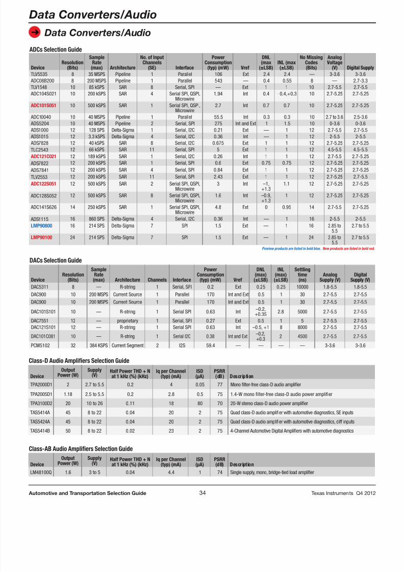
8/15/2019 TI Selection Guide
http://slidepdf.com/reader/full/ti-selection-guide 34/49
➔
34 Automotive and Transportation Selection Guide Texas Instruments Q4 2012
ADCs Selection Guide
DeviceResolution
(Bits)
SampleRate
(max) Architecture
No. of InputChannels
(SE) Interface
PowerConsumption
(typ) (mW) Vref
DNL(max
(±LSB)INL (max(±LSB)
No MissingCodes(Bits)
AnalogVoltage
(V) Digital SupplyTLV5535 8 35 MSPS Pipeline 1 Parallel 106 Ext 2.4 2.4 — 3-3.6 3-3.6
ADC08B200 8 200 MSPS Pipeline 1 Parallel 543 — 0.4 0.55 8 — 2.7-3.3TLV1548 10 85 kSPS SAR 8 Serial, SPI — Ext 1 1 10 2.7-5.5 2.7-5.5
ADC104S021 10 200 kSPS SAR 4 Serial SPI, QSPI,Microwire
1.94 Int 0.4 –0.4,+0.3 10 2.7-5.25 2.7-5.25
ADC101S051 10 500 kSPS SAR 1 Serial SPI, QSPI,Microwire
2.7 Int 0.7 0.7 10 2.7-5.25 2.7-5.25
ADC10040 10 40 MSPS Pipeline 1 Parallel 55.5 Int 0.3 0.3 10 2.7 to 3.6 2.5-3.6 ADS5204 10 40 MSPS Pipeline 2 Serial, SPI 275 Int and Ext 1 1.5 10 0-3.6 0-3.6 ADS1000 12 128 SPS Delta-Sigma 1 Serial, I2C 0.21 Ext — 1 12 2.7-5.5 2.7-5.5 ADS1015 12 3.3 kSPS Delta-Sigma 4 Serial, I2C 0.36 Int — 1 12 2-5.5 2-5.5 ADS7828 12 40 kSPS SAR 8 Serial, I2C 0.675 Ext 1 1 12 2.7-5.25 2.7-5.25TLC2543 12 66 kSPS SAR 11 Serial, SPI 5 Ext 1 1 12 4.5-5.5 4.5-5.5ADC121C021 12 189 kSPS SAR 1 Serial, I2C 0.26 Int 1 1 12 2.7-5.5 2.7-5.25 ADS7822 12 200 kSPS SAR 1 Serial, SPI 0.6 Ext 0.75 0.75 12 2.7-5.25 2.7-5.25 ADS7841 12 200 kSPS SAR 4 Serial, SPI 0.84 Ext 1 1 12 2.7-5.25 2.7-5.25TLV2553 12 200 kSPS SAR 11 Serial, SPI 2.43 Ext 1 1 12 2.7-5.25 2.7-5.5ADC122S051 12 500 kSPS SAR 2 Serial SPI, QSPI,
Microwire3 Int –1,
+1.31.1 12 2.7-5.25 2.7-5.25
ADC128S05212 500 kSPS SAR 8 Serial SPI, QSPI,Microwire 1.6 Int –0.9,+1.3 1 12 2.7-5.25 2.7-5.25
ADC141S626 14 250 kSPS SAR 1 Serial SPI, QSPI,Microwire
4.8 Ext 0 0.95 14 2.7-5.5 2.7-5.25
ADS1115 16 860 SPS Delta-Sigma 4 Serial, I2C 0.36 Int — 1 16 2-5.5 2-5.5LMP90800 16 214 SPS Delta-Sigma 7 SPI 1.5 Ext — 1 16 2.85 to
5.52.7 to 5.5
LMP90100 24 214 SPS Delta-Sigma 7 SPI 1.5 Ext — 1 24 2.85 to5.5
2.7 to 5.5
Preview products are listed in bold blue. New products are listed in bold red.
Class-D Audio Ampliers Selection Guide
DeviceOutput
Power (W)Supply
(V)Half Power THD + Nat 1 kHz (%) (kHz)
Iq per Channel(typ) (mA)
ISD(µA)
PSRR(dB) Description
TPA2000D1 2 2.7 to 5.5 0.2 4 0.05 77 Mono lter-free class-D audio amplier
TPA2005D1 1.18 2.5 to 5.5 0.2 2.8 0.5 75 1.4-W mono lter-free class-D audio power amplierTPA3100D2 20 10 to 26 0.11 18 80 70 20-W stereo class-D audio power amplier
TAS5414A 45 8 to 22 0.04 20 2 75 Quad class-D audio amplier with automotive diagnostics, SE inputs
TAS5424A 45 8 to 22 0.04 20 2 75 Quad class-D audio amplier with automotive diagnostics, diff inputs
TAS5414B 50 8 to 22 0.02 23 2 75 4-Channel Automotive Digital Ampliers with automotive diagnostics
Class-AB Audio Ampliers Selection Guide
DeviceOutput
Power (W)Supply
(V)Half Power THD + Nat 1 kHz (%) (kHz)
Iq per Channel(typ) (mA)
ISD(µA)
PSRR(dB) Description
LM48100Q 1.6 3 to 5 0.04 4.4 1 74 Single supply, mono, bridge-tied load amplier
DACs Selection Guide
DeviceResolution
(Bits)
SampleRate
(max) Architecture Channels Interface
PowerConsumption
(typ) (mW) Vref
DNL(max)(±LSB)
INL(max)(±LSB)
Settlingtime(ns)
AnalogSupply (V)
DigitalSupply (V)
DAC5311 8 — R-string 1 Serial, SPI 0.2 Ext 0.25 0.25 10000 1.8-5.5 1.8-5.5
DAC900 10 200 MSPS Current Source 1 Parallel 170 Int and Ext 0.5 1 30 2.7-5.5 2.7-5.5DAC900 10 200 MSPS Current Source 1 Parallel 170 Int and Ext 0.5 1 30 2.7-5.5 2.7-5.5
DAC101S101 10 — R-string 1 Serial SPI 0.63 Int –0.2,+0.35 2.8 5000 2.7-5.5 2.7-5.5
DAC7551 12 — proprietary 1 Serial, SPI 0.27 Ext 0.5 1 5 2.7-5.5 2.7-5.5DAC121S101 12 — R-string 1 Serial SPI 0.63 Int –0.5, +1 8 8000 2.7-5.5 2.7-5.5
DAC101C081 10 — R-string 1 Serial I2C 0.38 Int and Ext –0.2,+0.3 2 4500 2.7-5.5 2.7-5.5
PCM5102 32 384 KSPS Current Segment 2 I2S 59.4 — — — — 3-3.6 3-3.6
Data Converters/Audio
Data Converters/Audio
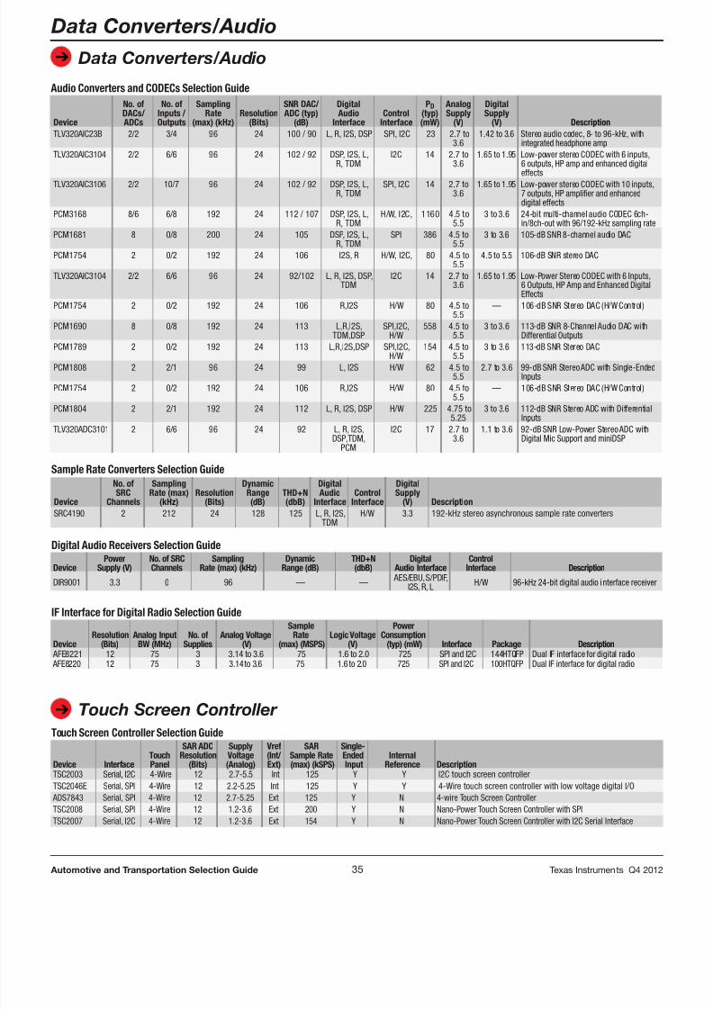
8/15/2019 TI Selection Guide
http://slidepdf.com/reader/full/ti-selection-guide 35/49
➔
35 Automotive and Transportation Selection Guide Texas Instruments Q4 2012
Sample Rate Converters Selection Guide
Device
No. ofSRC
Channels
SamplingRate (max)
(kHz)Resolution
(Bits)
DynamicRange(dB)
THD+N(dbB)
DigitalAudio
InterfaceControl
Interface
DigitalSupply
(V) DescriptionSRC4190 2 212 24 128 125 L, R, I2S,
TDM
H/W 3.3 192-kHz stereo asynchronous sample rate converters
Audio Converters and CODECs Selection Guide
Device
No. ofDACs/ADCs
No. ofInputs /Outputs
SamplingRate
(max) (kHz)Resolution
(Bits)
SNR DAC/ADC (typ)
(dB)
DigitalAudio
InterfaceControl
Interface
PD(typ)(mW)
AnalogSupply
(V)
DigitalSupply
(V) DescriptionTLV320AIC23B 2/2 3/4 96 24 100 / 90 L, R, I2S, DSP SPI, I2C 23 2.7 to
3.61.42 to 3.6 Stereo audio codec, 8- to 96-kHz, with
integrated headphone ampTLV320AIC3104 2/2 6/6 96 24 102 / 92 DSP, I2S, L,
R, TDMI2C 14 2.7 to
3.61.65 to 1.95 Low-power stereo CODEC with 6 inputs,
6 outputs, HP amp and enhanced digital
effectsTLV320AIC3106 2/2 10/7 96 24 102 / 92 DSP, I2S, L,
R, TDMSPI, I2C 14 2.7 to
3.61.65 to 1.95 Low-power stereo CODEC with 10 inputs
7 outputs, HP amplier and enhanceddigital effects
PCM3168 8/6 6/8 192 24 112 / 107 DSP, I2S, L,R, TDM
H/W, I2C, 1160 4.5 to5.5
3 to 3.6 24-bit multi-channel audio CODEC 6ch-in/8ch-out with 96/192-kHz sampling rate
PCM1681 8 0/8 200 24 105 DSP, I2S, L,R, TDM
SPI 386 4.5 to5.5
3 to 3.6 105-dB SNR 8-channel audio DAC
PCM1754 2 0/2 192 24 106 I2S, R H/W, I2C, 80 4.5 to5.5
4.5 to 5.5 106-dB SNR stereo DAC
TLV320AIC3104 2/2 6/6 96 24 92/102 L, R, I2S, DSP,TDM
I2C 14 2.7 to3.6
1.65 to 1.95 Low-Power Stereo CODEC with 6 Inputs,6 Outputs, HP Amp and Enhanced DigitalEffects
PCM1754 2 0/2 192 24 106 R,I2S H/W 80 4.5 to5.5
— 106-dB SNR Stereo DAC (H/W Control)
PCM1690 8 0/8 192 24 113 L,R,I2S,TDM,DSP
SPI,I2C,H/W
558 4.5 to5.5
3 to 3.6 113-dB SNR 8-Channel Audio DAC withDifferential Outputs
PCM1789 2 0/2 192 24 113 L,R,I2S,DSP SPI,I2C,H/W 154 4.5 to5.5 3 to 3.6 113-dB SNR Stereo DAC
PCM1808 2 2/1 96 24 99 L, I2S H/W 62 4.5 to5.5
2.7 to 3.6 99-dB SNR Stereo ADC with Single-EndeInputs
PCM1754 2 0/2 192 24 106 R,I2S H/W 80 4.5 to5.5
— 106-dB SNR Stereo DAC (H/W Control)
PCM1804 2 2/1 192 24 112 L, R, I2S, DSP H/W 225 4.75 to5.25
3 to 3.6 112-dB SNR Stereo ADC with DifferentiaInputs
TLV320ADC3101 2 6/6 96 24 92 L, R, I2S,DSP,TDM,
PCM
I2C 17 2.7 to3.6
1.1 to 3.6 92-dB SNR Low-Power Stereo ADC withDigital Mic Support and miniDSP
IF Interface for Digital Radio Selection Guide
DeviceResolution
(Bits)Analog Input
BW (MHz)No. of
SuppliesAnalog Voltage
(V)
SampleRate
(max) (MSPS)Logic Voltage
(V)
PowerConsumption (typ) (mW) Interface Package Description
AFE8221 12 75 3 3.14 to 3.6 75 1.6 to 2.0 725 SPI and I2C 144HTQFP Dual IF interface for digital radio AFE8220 12 75 3 3.14 to 3.6 75 1.6 to 2.0 725 SPI and I2C 100HTQFPDual IF interface for digital radio
Digital Audio Receivers Selection Guide
DevicePower
Supply (V)No. of SRCChannels
SamplingRate (max) (kHz)
DynamicRange (dB)
THD+N(dbB)
DigitalAudio Interface
ControlInterface Description
DIR9001 3.3 0 96 — — AES/EBU, S/PDIF,I2S, R, L H/W 96-kHz 24-bit digital audio interface receiver
Touch Screen Controller Selection Guide
Device InterfaceTouchPanel
SAR ADCResolution
(Bits)
SupplyVoltage(Analog)
Vref(Int/Ext)
SARSample Rate (max) (kSPS)
Single-Ended Input
InternalReference Description
TSC2003 Serial, I2C 4-Wire 12 2.7-5.5 Int 125 Y Y I2C touch screen controllerTSC2046E Serial, SPI 4-Wire 12 2.2-5.25 Int 125 Y Y 4-Wire touch screen controller with low voltage digital I/O
ADS7843 Serial, SPI 4-Wire 12 2.7-5.25 Ext 125 Y N 4-wire Touch Screen ControllerTSC2008 Serial, SPI 4-Wire 12 1.2-3.6 Ext 200 Y N Nano-Power Touch Screen Controller with SPITSC2007 Serial, I2C 4-Wire 12 1.2-3.6 Ext 154 Y N Nano-Power Touch Screen Controller with I2C Serial Interface
Data Converters/Audio
Data Converters/Audio
➔ Touch Screen Controller
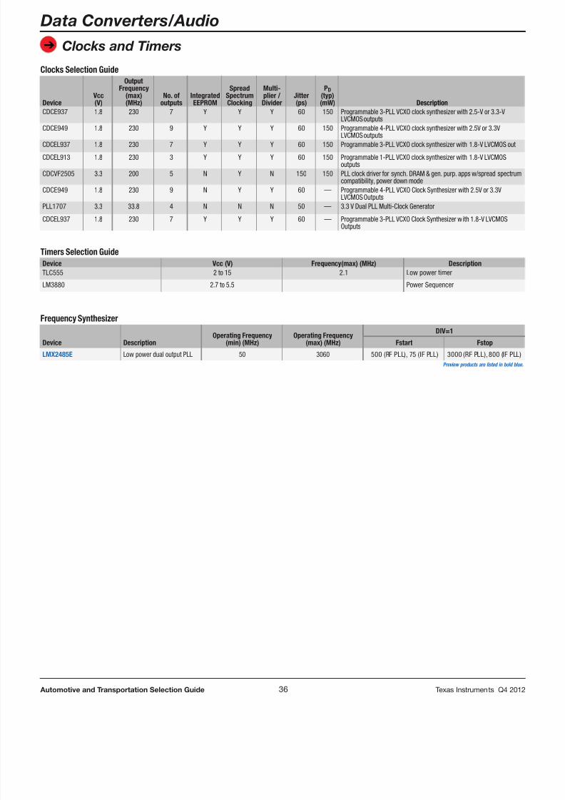
8/15/2019 TI Selection Guide
http://slidepdf.com/reader/full/ti-selection-guide 36/49
➔
36 Automotive and Transportation Selection Guide Texas Instruments Q4 2012
Timers Selection GuideDevice Vcc (V) Frequency(max) (MHz) DescriptionTLC555 2 to 15 2.1 Low power timer
LM3880 2.7 to 5.5 Power Sequencer
Frequency Synthesizer
DeviceOperating Frequency
(min) (MHz)Operating Frequency
(max) (MHz)
DIV=1
Description Fstart Fstop
LMX2485E Low power dual output PLL 50 3060 500 (RF PLL), 75 (IF PLL) 3000 (RF PLL), 800 (IF PLPreview products are listed in bold blue.
Clocks Selection Guide
DeviceVcc(V)
OutputFrequency
(max)(MHz)
No. ofoutputs
IntegratedEEPROM
SpreadSpectrumClocking
Multi-plier /Divider
Jitter(ps)
PD(typ)(mW) Description
CDCE937 1.8 230 7 Y Y Y 60 150 Programmable 3-PLL VCXO clock synthesizer with 2.5-V or 3.3-VLVCMOS outputs
CDCE949 1.8 230 9 Y Y Y 60 150 Programmable 4-PLL VCXO clock synthesizer with 2.5V or 3.3V
LVCMOS outputsCDCEL937 1.8 230 7 Y Y Y 60 150 Programmable 3-PLL VCXO clock synthesizer with 1.8-V LVCMOS
CDCEL913 1.8 230 3 Y Y Y 60 150 Programmable 1-PLL VCXO clock synthesizer with 1.8-V LVCMOSoutputs
CDCVF2505 3.3 200 5 N Y N 150 150 PLL clock driver for synch. DRAM & gen. purp. apps w/spread spectrcompatibility, power down mode
CDCE949 1.8 230 9 N Y Y 60 — Programmable 4-PLL VCXO Clock Synthesizer with 2.5V or 3.3VLVCMOS Outputs
PLL1707 3.3 33.8 4 N N N 50 — 3.3 V Dual PLL Multi-Clock Generator
CDCEL937 1.8 230 7 Y Y Y 60 — Programmable 3-PLL VCXO Clock Synthesizer with 1.8-V LVCMOSOutputs
Data Converters/Audio
Clocks and Timers
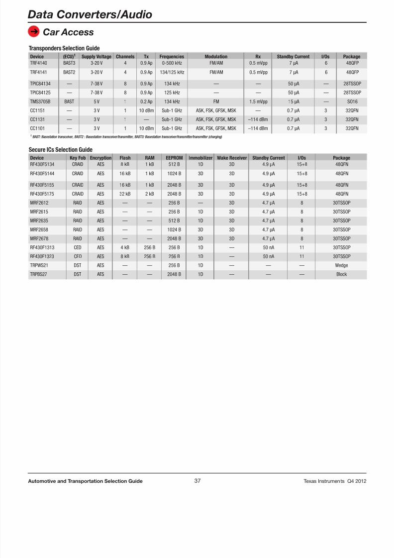
8/15/2019 TI Selection Guide
http://slidepdf.com/reader/full/ti-selection-guide 37/49
➔
37 Automotive and Transportation Selection Guide Texas Instruments Q4 2012
Data Converters/Audio
Car Access
Transponders Selection GuideDevice (ECU)1 Supply Voltage Channels Tx Frequencies Modulation Rx Standby Current I/Os PackageTRF4140 BAST3 3-20 V 4 0.9 Ap 0-500 kHz FM/AM 0.5 mVpp 7 μA 6 48QFP
TRF4141 BAST2 3-20 V 4 0.9 Ap 134/125 kHz FM/AM 0.5 mVpp 7 μA 6 48QFP
TPIC84134 — 7-38 V 8 0.9 Ap 134 kHz — — 50 μA — 28TSSOP
TPIC84125 — 7-38 V 8 0.9 Ap 125 kHz — — 50 μA — 28TSSOP
TMS3705B BAST 5 V 1 0.2 Ap 134 kHz FM 1.5 mVpp 15 μA — SO16
CC1151 — 3 V 1 10 dBm Sub-1 GHz ASK, FSK, GFSK, MSK — 0.7 μA 3 32QFN
CC1131 — 3 V 1 — Sub-1 GHz ASK, FSK, GFSK, MSK –114 dBm 0.7 μA 3 32QFN
CC1101 — 3 V 1 10 dBm Sub-1 GHz ASK, FSK, GFSK, MSK –114 dBm 0.7 μA 3 32QFN1 BAST: Basestation transceiver, BAST2 : Basestation transceiver/transmitter, BAST3: Basestation transceiver/transmitter/transmitter (charging)
Secure ICs Selection GuideDevice Key Fob Encryption Flash RAM EEPROM Immobilizer Wake Receiver Standby Current I/Os PackageRF430F5134 CRAID AES 8 kB 1 kB 512 B 1D 3D 4.9 μA 15+8 48QFN
RF430F5144 CRAID AES 16 kB 1 kB 1024 B 3D 3D 4.9 μA 15+8 48QFN
RF430F5155 CRAID AES 16 kB 1 kB 2048 B 3D 3D 4.9 μA 15+8 48QFN
RF430F5175 CRAID AES 32 kB 2 kB 2048 B 3D 3D 4.9 μA 15+8 48QFN
MRF2612 RAID AES — — 256 B — 3D 4.7 μA 8 30TSSOP
MRF2615 RAID AES — — 256 B 1D 3D 4.7 μA 8 30TSSOP
MRF2635 RAID AES — — 512 B 1D 3D 4.7 μA 8 30TSSOP
MRF2658 RAID AES — — 1024 B 3D 3D 4.7 μA 8 30TSSOP
MRF2678 RAID AES — — 2048 B 3D 3D 4.7 μA 8 30TSSOP
RF430F1313 CED AES 4 kB 256 B 256 B 1D — 50 nA 11 30TSSOP
RF430F1323 CED AES 8 kB 256 B 256 B 1D — 50 nA 11 30TSSOP
TRPWS21 DST AES — — 256 B 1D — — — Wedge
TRPBS27 DST AES — — 2048 B 1D — — — Block
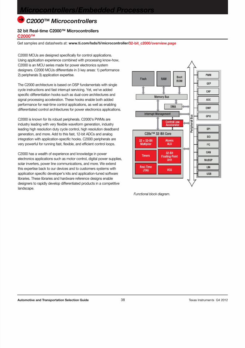
8/15/2019 TI Selection Guide
http://slidepdf.com/reader/full/ti-selection-guide 38/49
38 Automotive and Transportation Selection Guide Texas Instruments Q4 2012
➔
Microcontrollers/Embedded Processors
C2000™ Microcontrollers
32 bit Real-time C2000™ MicrocontrollersC2000™Get samples and datasheets at: www.ti.com/lsds/ti/microcontroller/ 32-bit_c2000/overview.page
C2000 MCUs are designed specifically for control applications.
Using application experience combined with processing know-how,C2000 is an MCU series made for power electronics systemdesigners. C2000 MCUs differentiate in 3 key areas: 1) performance2) peripherals 3) application expertise.
The C2000 architecture is based on DSP fundamentals with singlecycle instructions and fast interrupt servicing. Yet, we’ve addedspecific differentiation hooks such as dual-core architectures andsignal processing acceleration. These hooks enable both addedperformance for real-time control applications, as well as enablingdifferentiated control architectures for power electronics applications.
C2000 is known for its robust peripherals. C2000’s PWMs areindustry leading with very flexible waveform generation, industryleading high resolution duty cycle control, high resolution deadbandgeneration, and more. Add to this fast, 12-bit ADCs and analogintegration with application-specific hooks. C2000 peripherals arevery powerful for running fast, flexible, and efficient control loops.
C2000 has a wealth of experience and knowledge in powerelectronics applications such as motor control, digital power supplies,solar inverters, power line communications, and more. We extendthis expertise back to our devices and to customers systems withapplication specific developer’s kits and application-tuned softwarelibraries. These libraries and hardware reference designs enabledesigners to rapidly develop differentiated products in a competitivelandscape.
Functional block diagram.
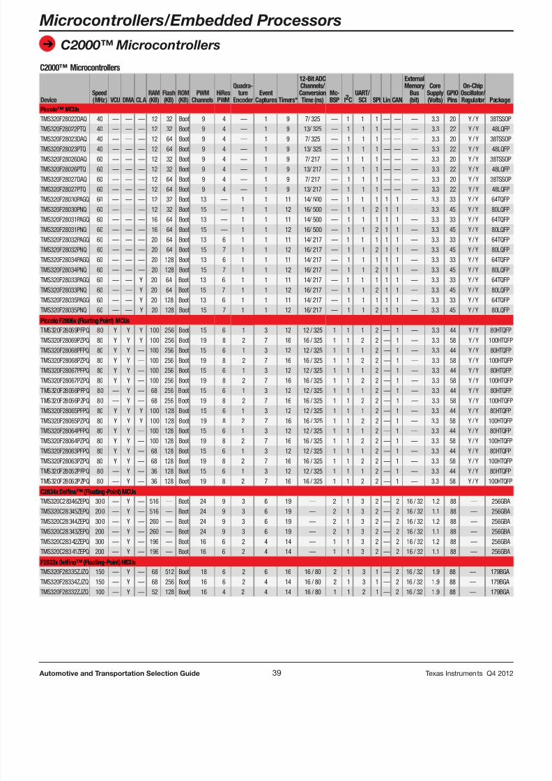
8/15/2019 TI Selection Guide
http://slidepdf.com/reader/full/ti-selection-guide 39/49
➔
39 Automotive and Transportation Selection Guide Texas Instruments Q4 2012
Microcontrollers/Embedded Processors
C2000™ Microcontrollers
C2000™ Microcontrollers
DeviceSpeed(MHz) VCU DMA CLA
RAM(KB)
Flash(KB)
ROM(KB)
PWM
ChannelsHiResPWM
Quadra-ture
EncoderEvent
Captures Timers*
12-Bit ADCChannels/ConversionTime (ns)
Mc-BSP I2C
UART/SCI SPI Lin CAN
ExternalMemory
Bus(bit)
CoreSupply(Volts)
GPIOPins
On-ChipOscillator/Regulator Package
Piccolo™ MCUsTMS320F28022DAQ 40 — — — 12 32 Boot 9 4 — 1 9 7/ 325 — 1 1 1 — — — 3.3 20 Y / Y 38TSSOPTMS320F28022PTQ 40 — — — 12 32 Boot 9 4 — 1 9 13/ 325 — 1 1 1 — — — 3.3 22 Y / Y 48LQFPTMS320F28023DAQ 40 — — — 12 64 Boot 9 4 — 1 9 7/ 325 — 1 1 1 — — — 3.3 20 Y / Y 38TSSOPTMS320F28023PTQ 40 — — — 12 64 Boot 9 4 — 1 9 13/ 325 — 1 1 1 — — — 3.3 22 Y / Y 48LQFPTMS320F28026DAQ 60 — — — 12 32 Boot 9 4 — 1 9 7/ 217 — 1 1 1 — — — 3.3 20 Y / Y 38TSSOPTMS320F28026PTQ 60 — — — 12 32 Boot 9 4 — 1 9 13/ 217 — 1 1 1 — — — 3.3 22 Y / Y 48LQFPTMS320F28027DAQ 60 — — — 12 64 Boot 9 4 — 1 9 7/ 217 — 1 1 1 — — — 3.3 20 Y / Y 38TSSOPTMS320F28027PTQ 60 — — — 12 64 Boot 9 4 — 1 9 13/ 217 — 1 1 1 — — — 3.3 22 Y / Y 48LQFPTMS320F28030PAGQ 60 — — — 12 32 Boot 13 — 1 1 11 14/ 500 — 1 1 1 1 1 — 3.3 33 Y / Y 64TQFPTMS320F28030PNQ 60 — — — 12 32 Boot 15 — 1 1 12 16/ 500 — 1 1 2 1 1 — 3.3 45 Y / Y 80LQFPTMS320F28031PAGQ 60 — — — 16 64 Boot 13 — 1 1 11 14/ 500 — 1 1 1 1 1 — 3.3 33 Y / Y 64TQFPTMS320F28031PNQ 60 — — — 16 64 Boot 15 — 1 1 12 16/ 500 — 1 1 2 1 1 — 3.3 45 Y / Y 80LQFPTMS320F28032PAGQ 60 — — — 20 64 Boot 13 6 1 1 11 14/ 217 — 1 1 1 1 1 — 3.3 33 Y / Y 64TQFPTMS320F28032PNQ 60 — — — 20 64 Boot 15 7 1 1 12 16/ 217 — 1 1 2 1 1 — 3.3 45 Y / Y 80LQFPTMS320F28034PAGQ 60 — — — 20 128 Boot 13 6 1 1 11 14/ 217 — 1 1 1 1 1 — 3.3 33 Y / Y 64TQFP
TMS320F28034PNQ 60 — — — 20 128 Boot 15 7 1 1 12 16/ 217 — 1 1 2 1 1 — 3.3 45 Y / Y 80LQFPTMS320F28033PAGQ 60 — — Y 20 64 Boot 13 6 1 1 11 14/ 217 — 1 1 1 1 1 — 3.3 33 Y / Y 64TQFPTMS320F28033PNQ 60 — — Y 20 64 Boot 15 7 1 1 12 16/ 217 — 1 1 2 1 1 — 3.3 45 Y / Y 80LQFPTMS320F28035PAGQ 60 — — Y 20 128 Boot 13 6 1 1 11 14/ 217 — 1 1 1 1 1 — 3.3 33 Y / Y 64TQFPTMS320F28035PNQ 60 — — Y 20 128 Boot 15 7 1 1 12 16/ 217 — 1 1 2 1 1 — 3.3 45 Y / Y 80LQFP
Piccolo F2806x (Floating Point) MCUsTMS320F28069PFPQ 80 Y Y Y 100 256 Boot 15 6 1 3 12 12 / 325 1 1 1 2 — 1 — 3.3 44 Y / Y 80HTQFTMS320F28069PZPQ 80 Y Y Y 100 256 Boot 19 8 2 7 16 16 / 325 1 1 2 2 — 1 — 3.3 58 Y / Y 100HTQFTMS320F28068PFPQ 80 Y Y — 100 256 Boot 15 6 1 3 12 12 / 325 1 1 1 2 — 1 — 3.3 44 Y / Y 80HTQFTMS320F28068PZPQ 80 Y Y — 100 256 Boot 19 8 2 7 16 16 / 325 1 1 2 2 — 1 — 3.3 58 Y / Y 100HTQFTMS320F28067PFPQ 80 Y Y — 100 256 Boot 15 6 1 3 12 12 / 325 1 1 1 2 — 1 — 3.3 44 Y / Y 80HTQFTMS320F28067PZPQ 80 Y Y — 100 256 Boot 19 8 2 7 16 16 / 325 1 1 2 2 — 1 — 3.3 58 Y / Y 100HTQFTMS320F28066PFPQ 80 — Y — 68 256 Boot 15 6 1 3 12 12 / 325 1 1 1 2 — 1 — 3.3 44 Y / Y 80HTQFTMS320F28066PZPQ 80 — Y — 68 256 Boot 19 8 2 7 16 16 / 325 1 1 2 2 — 1 — 3.3 58 Y / Y 100HTQFTMS320F28065PFPQ 80 Y Y Y 100 128 Boot 15 6 1 3 12 12 / 325 1 1 1 2 — 1 — 3.3 44 Y / Y 80HTQFTMS320F28065PZPQ 80 Y Y Y 100 128 Boot 19 8 2 7 16 16 / 325 1 1 2 2 — 1 — 3.3 58 Y / Y 100HTQFTMS320F28064PFPQ 80 Y Y — 100 128 Boot 15 6 1 3 12 12 / 325 1 1 1 2 — 1 — 3.3 44 Y / Y 80HTQFTMS320F28064PZPQ 80 Y Y — 100 128 Boot 19 8 2 7 16 16 / 325 1 1 2 2 — 1 — 3.3 58 Y / Y 100HTQFTMS320F28063PFPQ 80 Y Y — 68 128 Boot 15 6 1 3 12 12 / 325 1 1 1 2 — 1 — 3.3 44 Y / Y 80HTQFTMS320F28063PZPQ 80 Y Y — 68 128 Boot 19 8 2 7 16 16 / 325 1 1 2 2 — 1 — 3.3 58 Y / Y 100HTQFTMS320F28062PFPQ 80 — Y — 36 128 Boot 15 6 1 3 12 12 / 325 1 1 1 2 — 1 — 3.3 44 Y / Y 80HTQFTMS320F28062PZPQ 80 — Y — 36 128 Boot 19 8 2 7 16 16 / 325 1 1 2 2 — 1 — 3.3 58 Y / Y 100HTQF
C2834x Delno™ (Floating-Point) MCUs 19 2 7 16 16 / 325 1 1 2 2 - 1 58 Yes / Yes 100HTQFTMS320C28346ZEPQ 300 — Y — 516 — Boot 24 9 3 6 19 — 2 1 3 2 — 2 16 / 32 1.2 88 — 256GBATMS320C28345ZEPQ 200 — Y — 516 — Boot 24 9 3 6 19 — 2 1 3 2 — 2 16 / 32 1.1 88 — 256GBATMS320C28344ZEPQ 300 — Y — 260 — Boot 24 9 3 6 19 — 2 1 3 2 — 2 16 / 32 1.2 88 — 256GBATMS320C28343ZEPQ 200 — Y — 260 — Boot 24 9 3 6 19 — 2 1 3 2 — 2 16 / 32 1.1 88 — 256GBA
TMS320C28342ZEPQ 300 — Y — 196 — Boot 16 6 2 4 14 — 1 1 3 2 — 2 16 / 32 1.2 88 — 256GBATMS320C28341ZEPQ 200 — Y — 196 — Boot 16 6 2 4 14 — 1 1 3 2 — 2 16 / 32 1.1 88 — 256GBA
F2833x Delno™ (Floating-Point) MCUsTMS320F28335ZJZQ 150 — Y — 68 512 Boot 18 6 2 6 16 16 / 80 2 1 3 1 — 2 16 / 32 1.9 88 — 179BGA TMS320F28334ZJZQ 150 — Y — 68 256 Boot 16 6 2 4 14 16 / 80 2 1 3 1 — 2 16 / 32 1.9 88 — 179BGA TMS320F28332ZJZQ 100 — Y — 52 128 Boot 16 4 2 4 14 16 / 80 1 1 2 1 — 2 16 / 32 1.9 88 — 179BGA
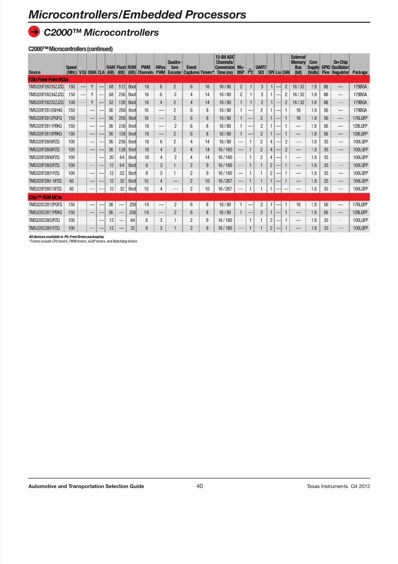
8/15/2019 TI Selection Guide
http://slidepdf.com/reader/full/ti-selection-guide 40/49
➔
40 Automotive and Transportation Selection Guide Texas Instruments Q4 2012
Microcontrollers/Embedded Processors
C2000™ Microcontrollers
C2000™ Microcontrollers (continued)
DeviceSpeed(MHz) VCU DMA CLA
RAM(KB)
Flash(KB)
ROM(KB)
PWM
ChannelsHiResPWM
Quadra-ture
EncoderEvent
Captures Timers*
12-Bit ADCChannels/ConversionTime (ns)
Mc-BSP I2C
UART/SCI SPI Lin CAN
ExternalMemory
Bus(bit)
CoreSupply(Volts)
GPIOPins
On-ChipOscillator/Regulator Package
F28x Fixed-Point MCUsTMS320F28235ZJZQ 150 — Y — 68 512 Boot 18 6 2 6 16 16 / 80 2 1 3 1 — 2 16 / 32 1.9 88 — 179BGA
TMS320F28234ZJZQ 150 — Y — 68 256 Boot 16 6 2 4 14 16 / 80 2 1 3 1 — 2 16 / 32 1.9 88 — 179BGA
TMS320F28232ZJZQ 100 — Y — 52 128 Boot 16 4 2 4 14 16 / 80 1 1 2 1 — 2 16 / 32 1.9 88 — 179BGA
TMS320F2812GHHQ 150 — — 36 256 Boot 16 — 2 6 8 16 / 80 1 — 2 1 — 1 16 1.9 56 — 179BGA
TMS320F2812PGFQ 150 — — 36 256 Boot 16 — 2 6 8 16 / 80 1 — 2 1 — 1 16 1.9 56 — 176LQFP
TMS320F2811PBKQ 150 — — 36 256 Boot 16 — 2 6 8 16 / 80 1 — 2 1 — 1 — 1.9 56 — 128LQFP
TMS320F2810PBKQ 150 — — 36 128 Boot 16 — 2 6 8 16 / 80 1 — 2 1 — 1 — 1.9 56 — 128LQFP
TMS320F2809PZQ 100 — — 36 256 Boot 16 6 2 4 14 16 / 80 — 1 2 4 — 2 — 1.8 35 — 100LQFP
TMS320F2808PZQ 100 — — 36 128 Boot 16 4 2 4 14 16 / 160 — 1 2 4 — 2 — 1.8 35 — 100LQFP
TMS320F2806PZQ 100 — — 20 64 Boot 16 4 2 4 14 16 / 160 — 1 2 4 — 1 — 1.8 35 — 100LQFP
TMS320F2802PZQ 100 — — 12 64 Boot 8 3 1 2 9 16 / 160 — 1 1 2 — 1 — 1.8 35 — 100LQFP
TMS320F2801PZQ 100 — — 12 32 Boot 8 3 1 2 9 16 / 160 — 1 1 2 — 1 — 1.8 35 — 100LQFP
TMS320F28016PZQ 60 — — 12 32 Boot 10 4 — 2 10 16 / 267 — 1 1 1 — 1 — 1.8 35 — 100LQFP
TMS320F28015PZQ 60 — — 12 32 Boot 10 4 — 2 10 16 / 267 — 1 1 1 — — — 1.8 35 — 100LQFP
C28x™ ROM MCUsTMS320C2812PGFQ 150 — — 36 — 256 16 — 2 6 8 16 / 80 1 — 2 1 — 1 16 1.9 56 — 176LQFP
TMS320C2811PBKQ 150 — — 36 — 256 16 — 2 6 8 16 / 80 1 — 2 1 — 1 — 1.9 56 — 128LQFP
TMS320C2802PZQ 100 — — 12 — 64 8 3 1 2 9 16 / 160 — 1 1 2 — 1 — 1.8 35 — 100LQFP
TMS320C2801PZQ 100 — — 12 — 32 8 3 1 2 9 16 / 160 — 1 1 2 — 1 — 1.8 35 — 100LQFP
All devices available in Pb-Free/Green packaging.*Timers include CPU timers, PWM timers, eCAP timers, and Watchdog timers.
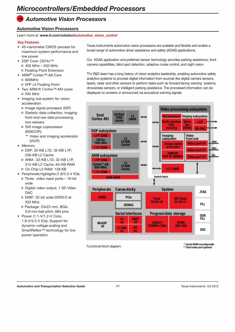
8/15/2019 TI Selection Guide
http://slidepdf.com/reader/full/ti-selection-guide 41/49
➔
41 Automotive and Transportation Selection Guide Texas Instruments Q4 2012
Microcontrollers/Embedded Processors
Automotive Vision Processors
Automotive Vision ProcessorsLearn more at: www.ti.com/solution/ automotive_vision_control
Key Features• 45–nanometer CMOS process for
maximum system performance and
low power• DSP Core: C674x™
° 450 MHz – 550 MHz
° Floating Point Extension• ARM ® Cortex™-A8 Core
° 600MHz
° VFP v3 Floating Point• Two ARM ® Cortex™-M3 cores
° 200 MHz• Imaging sub system for vision
acceleration
° Image signal processor (ISP)
° Statistic data collection, imagingfront end raw data processing,two resizers
° Still image coprocessor(SIMCOP):- Video and imaging accelerator
(VICP)• Memory
° DSP: 32-KB L1D, 32-KB L1P,256-KB L2 Cache
° ARM : 32-KB L1D, 32-KB L1P,512-KB L2 Cache, 64-KB RAM
° On Chip L3 RAM: 128 KB
• Peripherals highlights (1.8/3.3-V IOs)
° Three video input ports – 16-bitwide
° Digital video output, 1 SD VideoDAC
° EMIF: 32-bit wide DDR2/3 at333 MHz
° Package: 23x23 mm, BGA,0.8-mm ball pitch, 684 pins
• Power (1.1-V/1.2-V Core,1.8-V/3.3-V IOs): Support fordynamic voltage scaling and
SmartReflex™ technology for lowpower operation
Texas Instruments automotive vision processors are scalable and flexible and enable abroad range of automotive driver assistance and safety (ADAS) applications.
Our ADAS application and preferred sensor technology provides parking assistance, frontcamera capabilities, blind spot detection, adaptive cruise control, and night vision.
TI’s R&D team has a long history of vision analytics leadership, enabling automotive safetyanalytics systems to process digital information from sources like digital camera sensors,lasers, radar and other sensors to perform tasks such as forward facing warning systems,drowsiness sensors, or intelligent parking assistance. The processed information can bedisplayed on screens or announced via acoustical warning signals
Unied32KBcache
L1P 32KB
L1D 32KB
C674x ˜550-Mhz
L2512KB
Cache*
L1P 32KB
L1D 32KBRAM 64KB
Cortex™-A8600-MHz
L2512KBCache
DualCortex-M3
Video processing subsystem
DSP subsystem
ARM subsystem
Peripherals Connectivity
Serial interfaces
System
L264KB
De Interlacer
Multi-windowOSD
resizing
VideoEnc
(VENC)
Display subsystem
Image signalprocessor
SIMCOPVICP @ 400MHz
L3 128KB
EDMA Timer32-bit x8
I2Cx4
UARTx6
Program/data storage
DDR2/3333MHz (32b)
GPMC(8b/16b)
D-CANx2
SPIx4
WD Timer32-bit x1
Imagingsubsystem
Video port I/F
Video port I/F
Video port I/F
Videofront end
VIN0
* Cache/RAM recongurable ** Third video port optional
VIN1
ISS
PCIe
McASPx6
GEMAC
LCD
SD-DAC
JTAG
Switch fabric
PLL
DDRPLL
OSC
Functional block diagram.
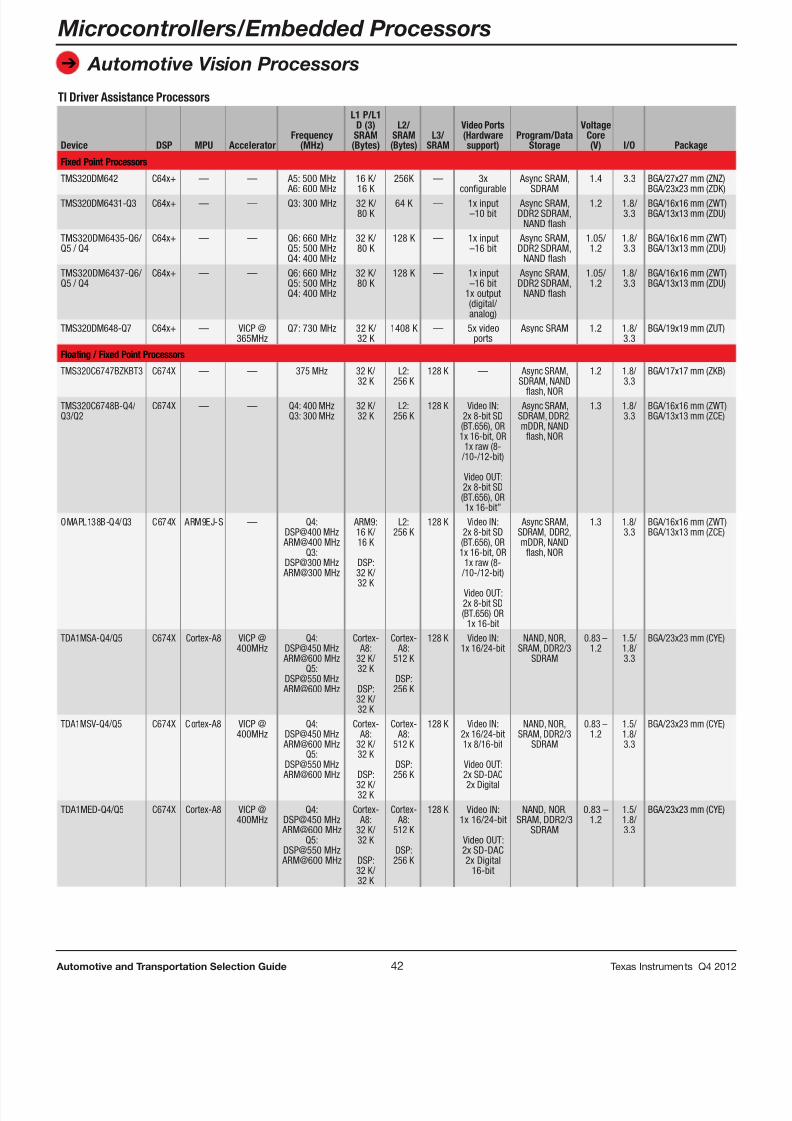
8/15/2019 TI Selection Guide
http://slidepdf.com/reader/full/ti-selection-guide 42/49
➔
42 Automotive and Transportation Selection Guide Texas Instruments Q4 2012
TI Driver Assistance Processors
Device DSP MPU AcceleratorFrequency
(MHz)
L1 P/L1D (3)
SRAM(Bytes)
L2/SRAM(Bytes)
L3/SRAM
Video Ports(Hardwaresupport)
Program/DataStorage
VoltageCore(V) I/O Package
Fixed Point Processors
TMS320DM642 C64x+ — — A5: 500 MHz
A6: 600 MHz
16 K/
16 K
256K — 3x
congurable
Async SRAM,
SDRAM
1.4 3.3 BGA/27x27 mm (ZNZ)
BGA/23x23 mm (ZDK)TMS320DM6431-Q3 C64x+ — — Q3: 300 MHz 32 K/80 K
64 K — 1x input–10 bit
Async SRAM,DDR2 SDRAM,
NAND ash
1.2 1.8/ 3.3
BGA/16x16 mm (ZWT)BGA/13x13 mm (ZDU)
TMS320DM6435-Q6/Q5 / Q4
C64x+ — — Q6: 660 MHzQ5: 500 MHzQ4: 400 MHz
32 K/80 K
128 K — 1x input–16 bit
Async SRAM,DDR2 SDRAM,
NAND ash
1.05/ 1.2
1.8/ 3.3
BGA/16x16 mm (ZWT)BGA/13x13 mm (ZDU)
TMS320DM6437-Q6/Q5 / Q4
C64x+ — — Q6: 660 MHzQ5: 500 MHzQ4: 400 MHz
32 K/80 K
128 K — 1x input–16 bit
1x output(digital/ analog)
Async SRAM,DDR2 SDRAM,
NAND ash
1.05/ 1.2
1.8/ 3.3
BGA/16x16 mm (ZWT)BGA/13x13 mm (ZDU)
TMS320DM648-Q7 C64x+ — VICP @365MHz
Q7: 730 MHz 32 K/ 32 K
1408 K — 5x videoports
Async SRAM 1.2 1.8/ 3.3
BGA/19x19 mm (ZUT)
Floating / Fixed Point Processors
TMS320C6747BZKBT3 C674X — — 375 MHz 32 K/ 32 K
L2:256 K
128 K — Async SRAM,SDRAM, NAND
ash, NOR
1.2 1.8/ 3.3
BGA/17x17 mm (ZKB)
TMS320C6748B-Q4/Q3/Q2
C674X — — Q4: 400 MHzQ3: 300 MHz
32 K/ 32 K
L2:256 K
128 K Video IN:2x 8-bit SD(BT.656), OR1x 16-bit, OR
1x raw (8- /10-/12-bit)
Video OUT:2x 8-bit SD(BT.656), OR1x 16-bit”
Async SRAM,SDRAM, DDR2,mDDR, NAND
ash, NOR
1.3 1.8/ 3.3
BGA/16x16 mm (ZWT)BGA/13x13 mm (ZCE)
OMAPL138B-Q4/Q3 C674X ARM9EJ-S — Q4:DSP@400 MHz
ARM@400 MHzQ3:
DSP@300 MHz ARM@300 MHz
ARM9:16 K/ 16 K
DSP:32 K/ 32 K
L2:256 K
128 K Video IN:2x 8-bit SD(BT.656), OR1x 16-bit, OR
1x raw (8- /10-/12-bit)
Video OUT:2x 8-bit SD(BT.656) OR
1x 16-bit
Async SRAM,SDRAM, DDR2,mDDR, NAND
ash, NOR
1.3 1.8/ 3.3
BGA/16x16 mm (ZWT)BGA/13x13 mm (ZCE)
TDA1MSA-Q4/Q5 C674X Cortex-A8 VICP @400MHz
Q4:DSP@450 MHz
ARM@600 MHzQ5:
DSP@550 MHz ARM@600 MHz
Cortex- A8:32 K/ 32 K
DSP:32 K/ 32 K
Cortex- A8:
512 K
DSP:256 K
128 K Video IN:1x 16/24-bit
NAND, NOR,SRAM, DDR2/3
SDRAM
0.83 –1.2
1.5/ 1.8/ 3.3
BGA/23x23 mm (CYE)
TDA1MSV-Q4/Q5 C674X C ortex-A8 VICP @400MHz
Q4:DSP@450 MHz
ARM@600 MHzQ5:
DSP@550 MHz
ARM@600 MHz
Cortex- A8:32 K/ 32 K
DSP:32 K/ 32 K
Cortex- A8:
512 K
DSP:
256 K
128 K Video IN:2x 16/24-bit1x 8/16-bit
Video OUT:
2x SD-DAC2x Digital
NAND, NOR,SRAM, DDR2/3
SDRAM
0.83 –1.2
1.5/ 1.8/ 3.3
BGA/23x23 mm (CYE)
TDA1MED-Q4/Q5 C674X Cortex-A8 VICP @400MHz
Q4:DSP@450 MHz
ARM@600 MHzQ5:
DSP@550 MHz ARM@600 MHz
Cortex- A8:32 K/ 32 K
DSP:32 K/ 32 K
Cortex- A8:
512 K
DSP:256 K
128 K Video IN:1x 16/24-bit
Video OUT:2x SD-DAC2x Digital
16-bit
NAND, NOR,SRAM, DDR2/3
SDRAM
0.83 –1.2
1.5/ 1.8/ 3.3
BGA/23x23 mm (CYE)
Microcontrollers/Embedded Processors
Automotive Vision Processors
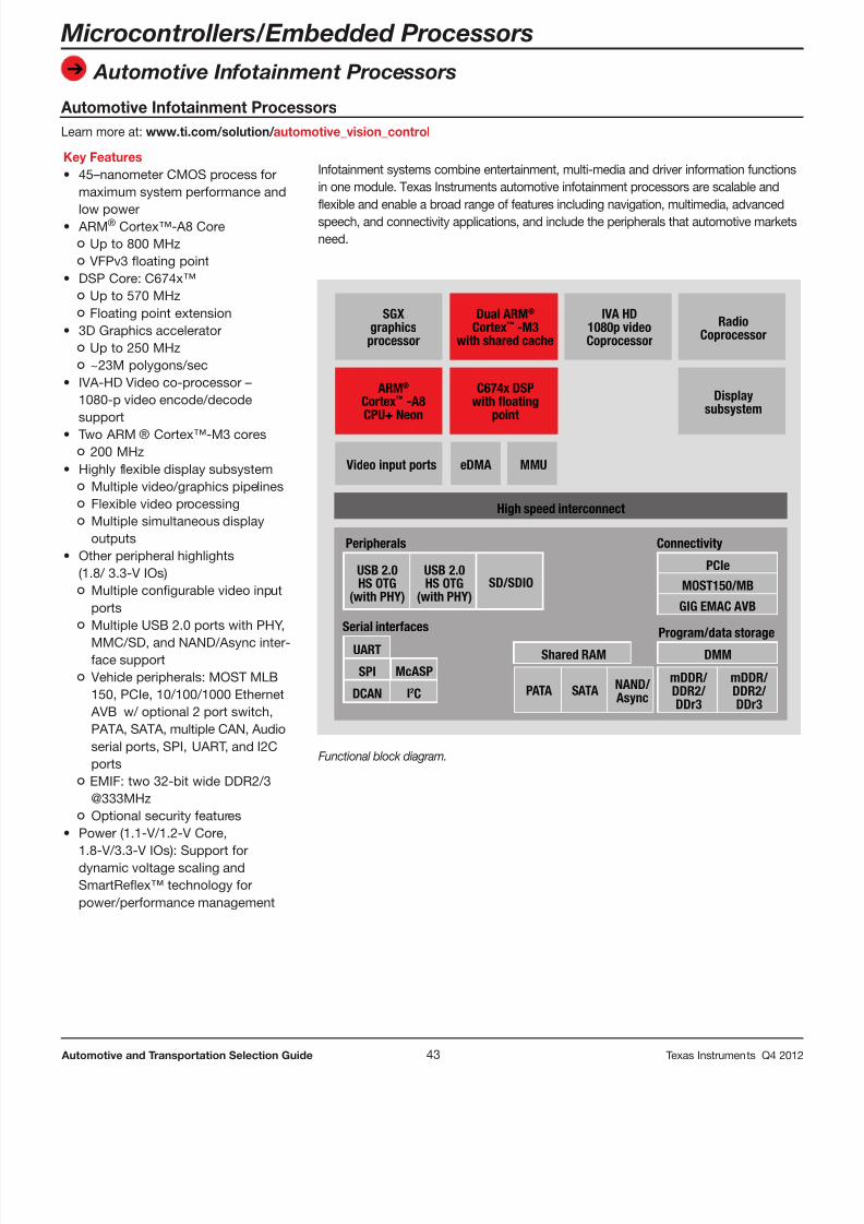
8/15/2019 TI Selection Guide
http://slidepdf.com/reader/full/ti-selection-guide 43/49
➔
43 Automotive and Transportation Selection Guide Texas Instruments Q4 2012
Microcontrollers/Embedded Processors
Automotive Infotainment Processors
Automotive Infotainment ProcessorsLearn more at: www.ti.com/solution/ automotive_vision_control
Key Features• 45–nanometer CMOS process for
maximum system performance and
low power• ARM ® Cortex™-A8 Core
° Up to 800 MHz
° VFPv3 floating point• DSP Core: C674x™
° Up to 570 MHz
° Floating point extension• 3D Graphics accelerator
° Up to 250 MHz
° ~23M polygons/sec• IVA-HD Video co-processor –
1080-p video encode/decode
support• Two ARM ® Cortex™-M3 cores
° 200 MHz• Highly flexible display subsystem
° Multiple video/graphics pipelines
° Flexible video processing
° Multiple simultaneous displayoutputs
• Other peripheral highlights(1.8/ 3.3-V IOs)
° Multiple configurable video inputports
° Multiple USB 2.0 ports with PHY,MMC/SD, and NAND/Async inter-face support
° Vehicle peripherals: MOST MLB150, PCIe, 10/100/1000 Ethernet
AVB w/ optional 2 port switch,PATA, SATA, multiple CAN, Audioserial ports, SPI, UART, and I2Cports
° EMIF: two 32-bit wide DDR2/3@333MHz
° Optional security features• Power (1.1-V/1.2-V Core,
1.8-V/3.3-V IOs): Support fordynamic voltage scaling andSmartReflex™ technology forpower/performance management
Infotainment systems combine entertainment, multi-media and driver information functionsin one module. Texas Instruments automotive infotainment processors are scalable andflexible and enable a broad range of features including navigation, multimedia, advancedspeech, and connectivity applications, and include the peripherals that automotive marketsneed.
Dual ARM®
Cortex™ -M3with shared cache
IVA HD1080p videoCoprocessor
RadioCoprocessor
Displaysubsystem
SGXgraphics
processor
C674x DSPwith oating
point
ARM®
Cortex™ -A8CPU+ Neon
Video input ports eDMA MMU
High speed interconnect
Peripherals
USB 2.0HS OTG
(with PHY)
Connectivity
PCIe
MOST150/MB
GIG EMAC AVB
Program/data storageDMMShared RAM
mDDR/DDR2/DDr3
mDDR/DDR2/DDr3
NAND/AsyncSATAPATA
Serial interfaces
UART
SPI
DCAN
McASP
I2C
USB 2.0HS OTG
(with PHY)SD/SDIO
Functional block diagram.
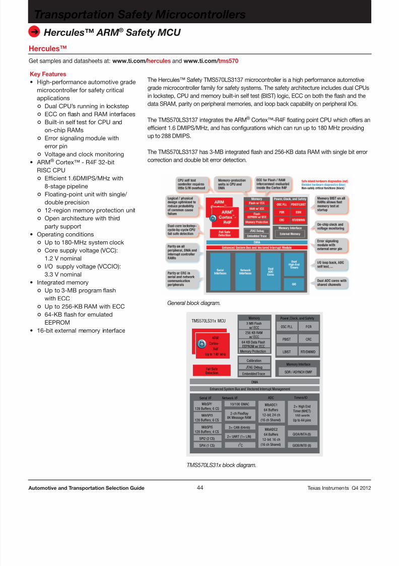
8/15/2019 TI Selection Guide
http://slidepdf.com/reader/full/ti-selection-guide 44/49
44 Automotive and Transportation Selection Guide Texas Instruments Q4 2012
➔
Hercules™
Get samples and datasheets at: www.ti.com/ hercules and www.ti.com/ tms570
Transportation Safety Microcontrollers
Hercules™ ARM ® Safety MCU
Key Features• High-performance automotive grade
microcontroller for safety critical
applications
° Dual CPU’s running in lockstep ° ECC on flash and RAM interfaces ° Built-in self test for CPU and
on-chip RAMs ° Error signaling module with
error pin ° Voltage and clock monitoring• ARM ® Cortex™ - R4F 32-bit
RISC CPU
° Efficient 1.6DMIPS/MHz with8-stage pipeline
° Floating-point unit with single/double precision
° 12-region memory protection unit ° Open architecture with third
party support• Operating conditions
° Up to 180-MHz system clock ° Core supply voltage (VCC):
1.2 V nominal ° I/O supply voltage (VCCIO):
3.3 V nominal• Integrated memory
° Up to 3-MB program flash
with ECC ° Up to 256-KB RAM with ECC ° 64-KB flash for emulated
EEPROM• 16-bit external memory interface
The Hercules™ Safety TMS570LS3137 microcontroller is a high performance automotivegrade microcontroller family for safety systems. The safety architecture includes dual CPUs
in lockstep, CPU and memory built-in self test (BIST) logic, ECC on both the flash and thedata SRAM, parity on peripheral memories, and loop back capability on peripheral IOs.
The TMS570LS3137 integrates the ARM ® Cortex™-R4F floating point CPU which offers anefficient 1.6 DMIPS/MHz, and has configurations which can run up to 180 MHz providingup to 288 DMIPS.
The TMS570LS3137 has 3-MB integrated flash and 256-KB data RAM with single bit errorcorrection and double bit error detection.
3 MB Flashw/ ECC
TMS570LS31x MCU
SDR / ASYNCH EMIFFail SafeDetection
MibSPI1128 Buffers; 6 CS
MibSPI3128 Buffers; 6 CS
MibSPI5128 Buffers; 4 CS
SPI2 (2 CS)
SPI4 (1 CS)
10/100 EMAC MibADC164 Buffers
12-bit, 24 ch(16 ch Shared)
MibADC264 Buffers
12-bit, 16 ch(16 ch Shared)
2× High EndTimer (NHET)
160 wordsUp to 44 pins
2-ch FlexRay8K Message RAM
3× CAN (64mb)
2× UART (1× LIN)GIOA/INTA (8)
GIOB/INTB (8)I C2
DMA
Serial I/F Network I/F ADC Timers/IO
Enhanced System Bus and Vectored Interrupt Management
OSC PLL POR
PBIST CRC
LBIST RTI/DWWD
64 KB Data FlashEEPROM w/ ECC
Calibration
JTAG Debug
Memory Power,Clock, and Safety
Memory Interface
Embedded Trace
256 KB RAMw/ ECC
ARM
Cortex -
R4F
™
160MHz
ARM
Cortex-
R4FUp to 180 MHz
Memory Protection
General block diagram.
TMS570LS31x block diagram.
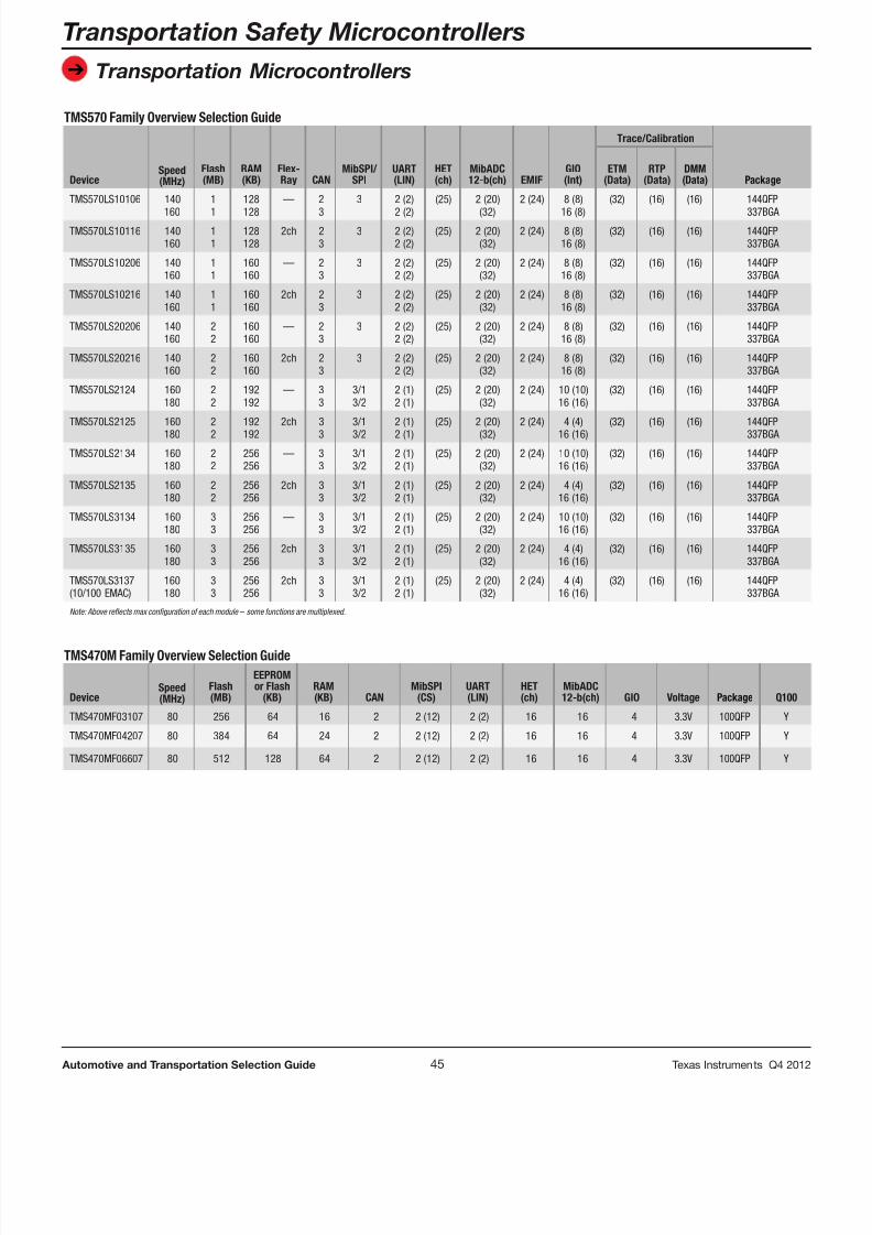
8/15/2019 TI Selection Guide
http://slidepdf.com/reader/full/ti-selection-guide 45/49
➔
45 Automotive and Transportation Selection Guide Texas Instruments Q4 2012
TMS470M Family Overview Selection Guide
DeviceSpeed(MHz)
Flash(MB)
EEPROMor Flash
(KB)RAM(KB) CAN
MibSPI(CS)
UART(LIN)
HET(ch)
MibADC12-b(ch) GIO Voltage Package Q100
TMS470MF03107 80 256 64 16 2 2 (12) 2 (2) 16 16 4 3.3V 100QFP Y
TMS470MF04207 80 384 64 24 2 2 (12) 2 (2) 16 16 4 3.3V 100QFP Y
TMS470MF06607 80 512 128 64 2 2 (12) 2 (2) 16 16 4 3.3V 100QFP Y
TMS570 Family Overview Selection Guide
DeviceSpeed(MHz)
Flash(MB)
RAM(KB)
Flex-Ray CAN
MibSPI/SPI
UART(LIN)
HET(ch)
MibADC12-b(ch) EMIF
GIO(Int)
Trace/Calibration
ETM(Data)
RTP(Data)
DMM(Data) Package
TMS570LS10106 140
160
1
1
128
128
— 2
3
3 2 (2)
2 (2)
(25) 2 (20)
(32)
2 (24) 8 (8)
16 (8)
(32) (16) (16) 144QFP
337BGA TMS570LS10116 140
16011
128128
2ch 23
3 2 (2)2 (2)
(25) 2 (20)(32)
2 (24) 8 (8)16 (8)
(32) (16) (16) 144QFP337BGA
TMS570LS10206 140160
11
160160
— 23
3 2 (2)2 (2)
(25) 2 (20)(32)
2 (24) 8 (8)16 (8)
(32) (16) (16) 144QFP337BGA
TMS570LS10216 140160
11
160160
2ch 23
3 2 (2)2 (2)
(25) 2 (20)(32)
2 (24) 8 (8)16 (8)
(32) (16) (16) 144QFP337BGA
TMS570LS20206 140160
22
160160
— 23
3 2 (2)2 (2)
(25) 2 (20)(32)
2 (24) 8 (8)16 (8)
(32) (16) (16) 144QFP337BGA
TMS570LS20216 140160
22
160160
2ch 23
3 2 (2)2 (2)
(25) 2 (20)(32)
2 (24) 8 (8)16 (8)
(32) (16) (16) 144QFP337BGA
TMS570LS2124 160180
22
192192
— 33
3/13/2
2 (1)2 (1)
(25) 2 (20)(32)
2 (24) 10 (10)16 (16)
(32) (16) (16) 144QFP337BGA
TMS570LS2125 160180 22 192192 2ch 33 3/13/2 2 (1)2 (1) (25) 2 (20)(32) 2 (24) 4 (4)16 (16) (32) (16) (16) 144QFP337BGA
TMS570LS2134 160180
22
256256
— 33
3/13/2
2 (1)2 (1)
(25) 2 (20)(32)
2 (24) 10 (10)16 (16)
(32) (16) (16) 144QFP337BGA
TMS570LS2135 160180
22
256256
2ch 33
3/13/2
2 (1)2 (1)
(25) 2 (20)(32)
2 (24) 4 (4)16 (16)
(32) (16) (16) 144QFP337BGA
TMS570LS3134 160180
33
256256
— 33
3/13/2
2 (1)2 (1)
(25) 2 (20)(32)
2 (24) 10 (10)16 (16)
(32) (16) (16) 144QFP337BGA
TMS570LS3135 160180
33
256256
2ch 33
3/13/2
2 (1)2 (1)
(25) 2 (20)(32)
2 (24) 4 (4)16 (16)
(32) (16) (16) 144QFP337BGA
TMS570LS3137(10/100 EMAC)
160180
33
256256
2ch 33
3/13/2
2 (1)2 (1)
(25) 2 (20)(32)
2 (24) 4 (4)16 (16)
(32) (16) (16) 144QFP337BGA
Note: Above reflects max configuration of each module – some functions are multiplexed.
T ransportation Safety Microcontrollers
Transportation Microcontrollers

8/15/2019 TI Selection Guide
http://slidepdf.com/reader/full/ti-selection-guide 46/49
Receive Updates on TI’s Solutionsfor Transportation Applications
By registering with my.TI
and telling us your areas
of interest by application,
product, etc., you
can receive the latest
information valuable to
you. To receive automotive
updates, be sure to select
“Automotive” under
“Edit Areas of Interest”
WEBENCH
®
Design CenterGet results faster with easy-to-use design tools that deliver custom results.
Quickly compare performanceacross multiple parametersfor complete systems
• Designer Series–Single-circuit design tools
• Architect Series– Advanced hierarchical design tools
• Unique Design Features– Visualizer and Optimizer Dial
www.ti.com/webench
8/15/2019 TI Selection Guide
http://slidepdf.com/reader/full/ti-selection-guide 47/49
To download these guides, please visit:www.ti.com/selection
Automotive Processors
Amps & Linear
Audio
Battery Management
C2000™ Microcontrollers
Clocks & TimersData Converters
High Reliability
Interface
LED
Logic
Power Management
RFID Systems
RF/IF Solutions
Standard Linear
Temperature Sensors and Monitoring
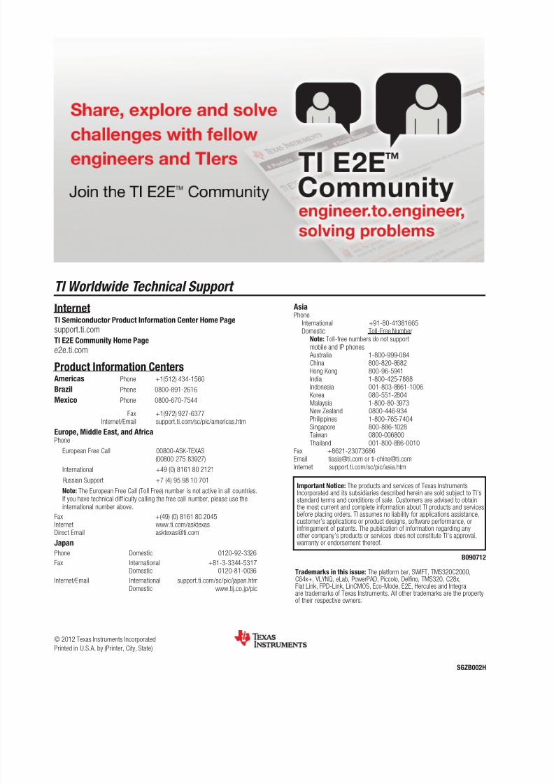
8/15/2019 TI Selection Guide
http://slidepdf.com/reader/full/ti-selection-guide 48/49
TI Worldwide Technical Support InternetTI Semiconductor Product Information Center Home Pagesupport.ti.comTI E2E Community Home Pagee2e.ti.com
Product Information CentersAmericas Phone +1(512) 434-1560Brazil Phone 0800-891-2616
Mexico Phone 0800-670-7544
Fax +1(972) 927-6377 Internet/Email support.ti.com/sc/pic/americas.htm
Europe, Middle East, and AfricaPhone European Free Call 00800-ASK-TEXAS
(00800 275 83927) International +49 (0) 8161 80 2121
Russian Support +7 (4) 95 98 10 701 Note: The European Free Call (Toll Free) number is not active in all countries.
If you have technical diff iculty calling the free call number, please use theinternational number above.
Fax +(49) (0) 8161 80 2045Internet www.ti.com/asktexasDirect Email [email protected]
JapanPhone Domestic 0120-92-3326Fax International +81-3-3344-5317 Domestic 0120-81-0036Internet/Email International support.ti.com/sc/pic/japan.htm Domestic www.tij.co.jp/pic
AsiaPhone International +91-80-41381665 Domestic Toll-Free Number Note: Toll-free numbers do not support
mobile and IP phones. Australia 1-800-999-084 China 800-820-8682 Hong Kong 800-96-5941 India 1-800-425-7888 Indonesia 001-803-8861-1006 Korea 080-551-2804 Malaysia 1-800-80-3973 New Zealand 0800-446-934 Philippines 1-800-765-7404 Singapore 800-886-1028 Taiwan 0800-006800 Thailand 001-800-886-0010Fax +8621-23073686Email [email protected] or [email protected] support.ti.com/sc/pic/asia.htm
B090712
SGZB002H
Important Notice: The products and services of Texas InstrumentsIncorporated and its subsidiaries described herein are sold subject to TI’sstandard terms and conditions of sale. Customers are advised to obtainthe most current and complete information about TI products and servicesbefore placing orders. TI assumes no liability for applications assistance,customer’s applications or product designs, software performance, orinfringement of patents. The publication of information regarding anyother company’s products or services does not constitute TI’s approval,warranty or endorsement thereof.
© 2012 Texas Instruments IncorporatedPrinted in U.S.A. by (Printer, City, State)
Trademarks in this issue: The platform bar, SWIFT, TMS320C2000,C64x+, VLYNQ, eLab, PowerPAD, Piccolo, Delfino, TMS320, C28x,Flat Link, FPD-Link, LinCMOS, Eco-Mode, E2E, Hercules and Integraare trademarks of Texas Instruments. All other trademarks are the propertyof their respective owners.
8/15/2019 TI Selection Guide
http://slidepdf.com/reader/full/ti-selection-guide 49/49
IMPORTANT NOTICE
Texas Instruments Incorporated and its subsidiaries (TI) reserve the right to make corrections, enhancements, improvements and otherchanges to its semiconductor products and services per JESD46, latest issue, and to discontinue any product or service per JESD48, latestissue. Buyers should obtain the latest relevant information before placing orders and should verify that such information is current andcomplete. All semiconductor products (also referred to herein as “components”) are sold subject to TI’s terms and conditions of salesupplied at the time of order acknowledgment.
TI warrants performance of its components to the specifications applicable at the time of sale, in accordance with the warranty in TI’s termsand conditions of sale of semiconductor products. Testing and other quality control techniques are used to the extent TI deems necessaryto support this warranty. Except where mandated by applicable law, testing of all parameters of each component is not necessarilyperformed.
TI assumes no liability for applications assistance or the design of Buyers’ products. Buyers are responsible for their products andapplications using TI components. To minimize the risks associated with Buyers’ products and applications, Buyers should provideadequate design and operating safeguards.
TI does not warrant or represent that any license, either express or implied, is granted under any patent right, copyright, mask work right, orother intellectual property right relating to any combination, machine, or process in which TI components or services are used. Informationpublished by TI regarding third-party products or services does not constitute a license to use such products or services or a warranty orendorsement thereof. Use of such information may require a license from a third party under the patents or other intellectual property of thethird party, or a license from TI under the patents or other intellectual property of TI.
Reproduction of significant portions of TI information in TI data books or data sheets is permissible only if reproduction is without alterationand is accompanied by all associated warranties, conditions, limitations, and notices. TI is not responsible or liable for such altereddocumentation. Information of third parties may be subject to additional restrictions.
Resale of TI components or services with statements different from or beyond the parameters stated by TI for that component or service
voids all express and any implied warranties for the associated TI component or service and is an unfair and deceptive business practice.TI is not responsible or liable for any such statements.
Buyer acknowledges and agrees that it is solely responsible for compliance with all legal, regulatory and safety-related requirementsconcerning its products, and any use of TI components in its applications, notwithstanding any applications-related information or supportthat may be provided by TI. Buyer represents and agrees that it has all the necessary expertise to create and implement safeguards whichanticipate dangerous consequences of failures, monitor failures and their consequences, lessen the likelihood of failures that might causeharm and take appropriate remedial actions. Buyer will fully indemnify TI and its representatives against any damages arising out of the useof any TI components in safety-critical applications.
In some cases, TI components may be promoted specifically to facilitate safety-related applications. With such components, TI’s goal is tohelp enable customers to design and create their own end-product solutions that meet applicable functional safety standards andrequirements. Nonetheless, such components are subject to these terms.
No TI components are authorized for use in FDA Class III (or similar life-critical medical equipment) unless authorized officers of the partieshave executed a special agreement specifically governing such use.
Only those TI components which TI has specifically designated as military grade or “enhanced plastic” are designed and intended for use inmilitary/aerospace applications or environments. Buyer acknowledges and agrees that any military or aerospace use of TI componentswhich have not been so designated is solely at the Buyer's risk, and that Buyer is solely responsible for compliance with all legal andregulatory requirements in connection with such use.
TI has specifically designated certain components which meet ISO/TS16949 requirements, mainly for automotive use. Components whichhave not been so designated are neither designed nor intended for automotive use; and TI will not be responsible for any failure of suchcomponents to meet such requirements.
Products Applications
Audio www.ti.com/audio Automotive and Transportation www.ti.com/automotive
Amplifiers amplifier.ti.com Communications and Telecom www.ti.com/communications
Data Converters dataconverter.ti.com Computers and Peripherals www.ti.com/computers
DLP® Products www.dlp.com Consumer Electronics www.ti.com/consumer-apps
DSP dsp.ti.com Energy and Lighting www.ti.com/energy
Clocks and Timers www.ti.com/clocks Industrial www.ti.com/industrial
Interface interface.ti.com Medical www.ti.com/medical
Logic logic.ti.com Security www.ti.com/security
Power Mgmt power.ti.com Space, Avionics and Defense www.ti.com/space-avionics-defense
Microcontrollers microcontroller.ti.com Video and Imaging www.ti.com/video
RFID www.ti-rfid.com
OMAP Applications Processors www.ti.com/omap TI E2E Community e2e.ti.com
Wireless Connectivity www.ti.com/wirelessconnectivity