Embed Size (px)
DESCRIPTION
Timing Issues for DSM. R. Brayton U.C. Berkeley. Caveats. This talk is about a work in progress Much of the work is roughly described with the idea of just communicating the general thrust. - PowerPoint PPT Presentation
Citation preview
12/5/97 1
Timing Issues for DSMTiming Issues for DSMTiming Issues for DSMTiming Issues for DSM
R. BraytonU.C. Berkeley
12/5/97 Tau97 2
Caveats
This talk is about a work in progressMuch of the work is roughly described
with the idea of just communicating the general thrust.
Many details remain to be decided and currently several algorithms are being programmed for experimental purposes.
We are just in the middle of many studies and depending on their results, the direction of the project may change.
12/5/97 Tau97 3
OutlineOutline
Introduction - DSM project at BerkeleyOur timing abstraction and motivationTiming driven placement (wireplanning)
slicing approach programming approach matching approach
Iterated logic decompositionLogic rip-up and re-routeTechnology aspects
12/5/97 Tau97 4
Overview
Two levels of approach electrical and technology level logic level using timing abstraction
Electrical level used to insure reality predict technology dimensions place and wire transistors to create leaf cells
using Cadence’s LAS tool or CADABRA extract parasitics using SPACE or FASTCAP simulate using SPICE with advanced BSIM model
12/5/97 Tau97 5
Overview
Logic level works with a timing abstraction (to be explained) we need to be sure that abstraction is correct
(thus electrical experiments)Currently cross-talk noise effects on
timing ignoredImmediate goal is to build combinational
logic macros that meet timing constraints sequential circuits can be handled similarly
12/5/97 Tau97 6
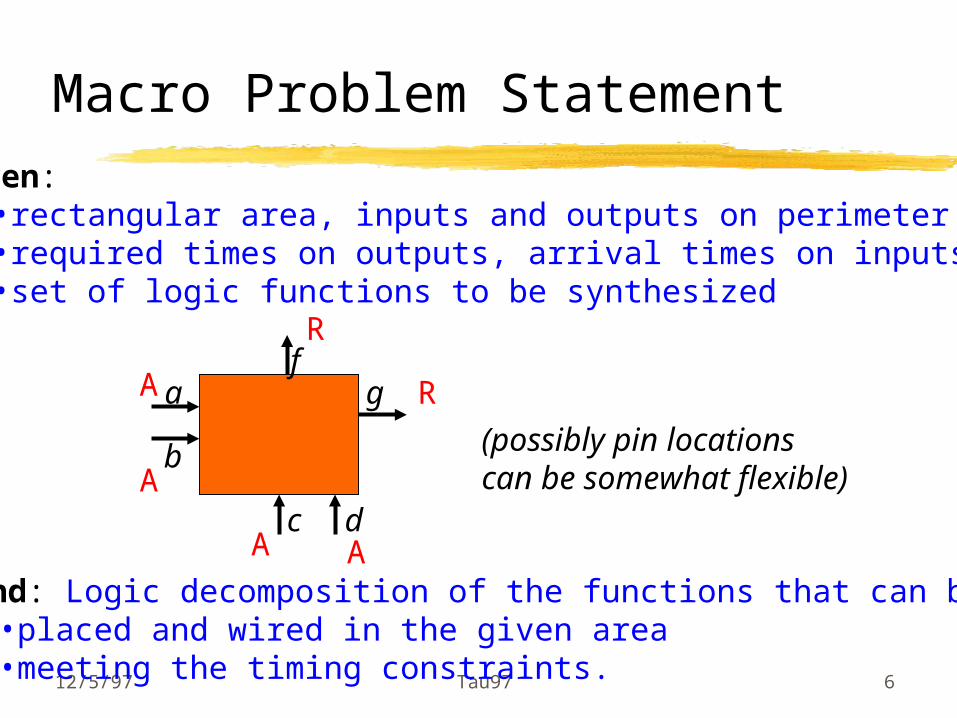
Macro Problem StatementGiven:
•rectangular area, inputs and outputs on perimeter. •required times on outputs, arrival times on inputs. •set of logic functions to be synthesized
(possibly pin locations can be somewhat flexible)
Find: Logic decomposition of the functions that can be: •placed and wired in the given area •meeting the timing constraints.
R
R
A
A
A A
a
b
c d
fg
12/5/97 Tau97 7
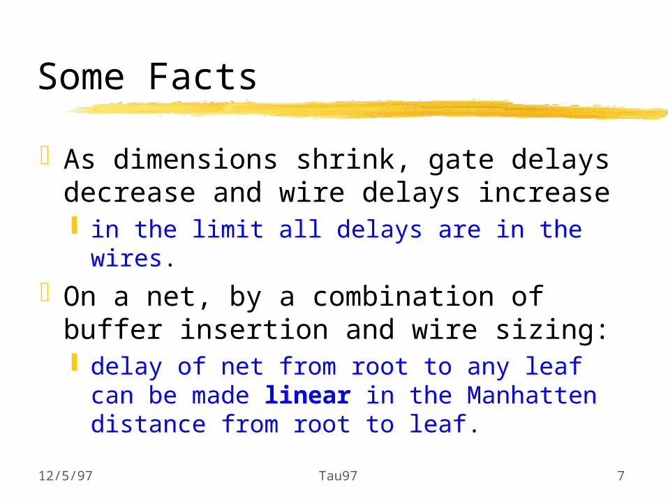
Some Facts
As dimensions shrink, gate delays decrease and wire delays increase in the limit all delays are in the wires.
On a net, by a combination of buffer insertion and wire sizing: delay of net from root to any leaf can be
made linear in the Manhatten distance from root to leaf.
12/5/97 Tau97 8
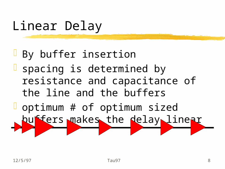
Linear Delay
By buffer insertionspacing is determined by resistance
and capacitance of the line and the buffers
optimum # of optimum sized buffers makes the delay linear
12/5/97 Tau97 9
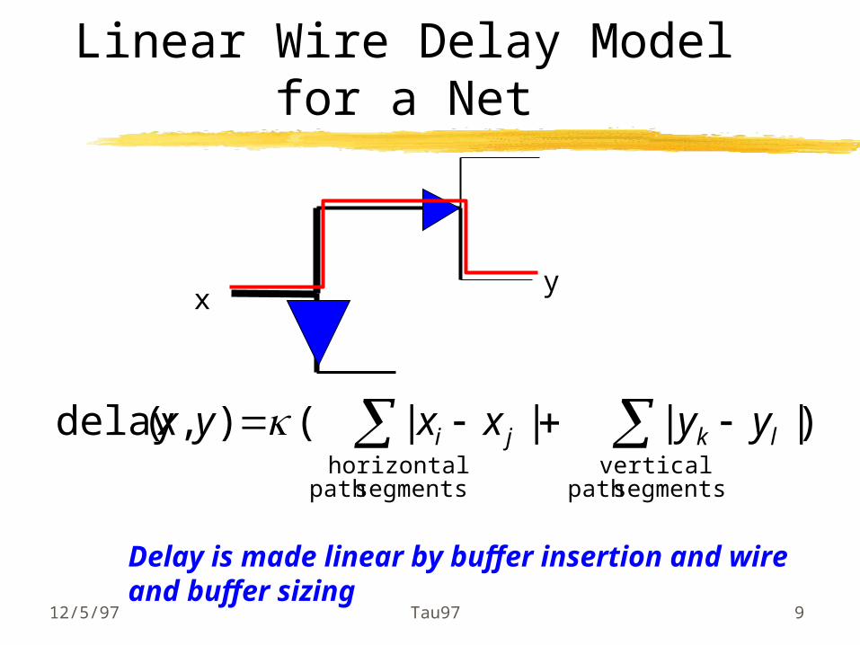
)||||(),(delay
segmentspath vertical
segmentspath horizontal
lkji yyxxyx
Linear Wire Delay Model for a Net
Delay is made linear by buffer insertion and wireand buffer sizing
xy
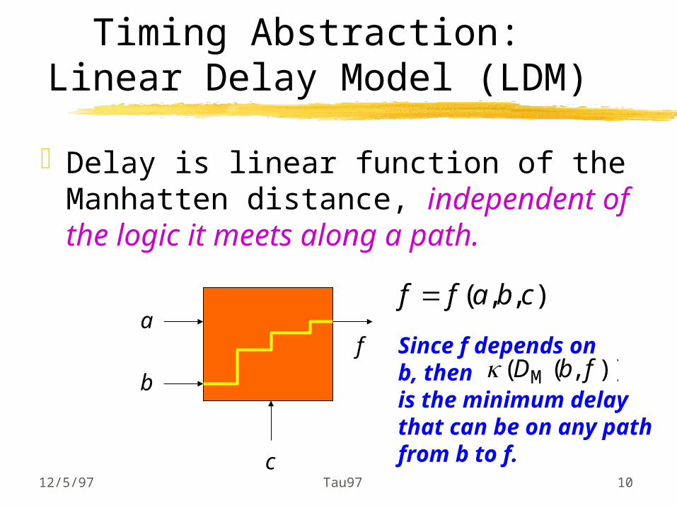
12/5/97 Tau97 10
f Since f depends onb, then is the minimum delaythat can be on any path from b to f.
)),(( M fbD
Timing Abstraction: Linear Delay Model (LDM)
Delay is linear function of the Manhatten distance, independent of the logic it meets along a path.
a
b
c
),,( cbaff
12/5/97 Tau97 11
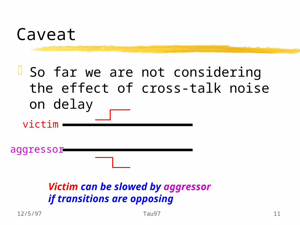
Caveat
So far we are not considering the effect of cross-talk noise on delay
victim
aggressor
Victim can be slowed by aggressor if transitions are opposing
12/5/97 Tau97 12
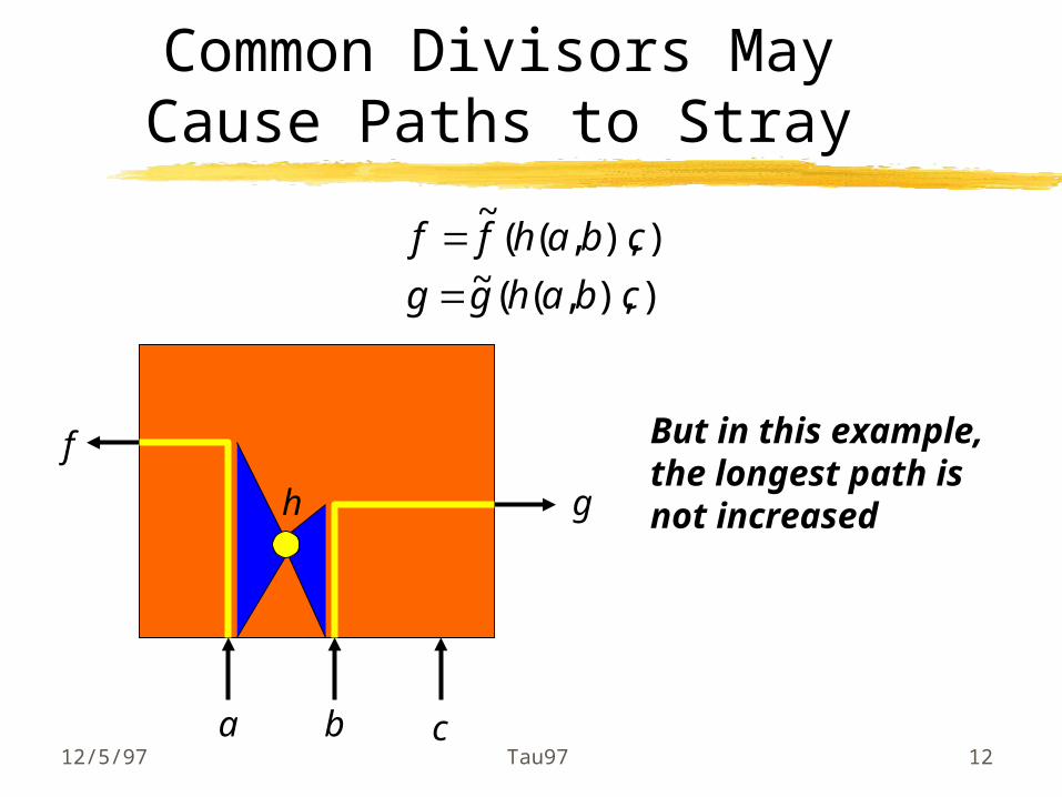
Common Divisors May Cause Paths to Stray
)),,((~)),,((
~
cbahgg
cbahff
a b c
f
gh
But in this example,the longest path isnot increased
12/5/97 Tau97 13
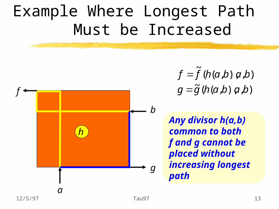
Example Where Longest Path Must be Increased
a
b
f
g
h
),),,((~),),,((
~
babahgg
babahff
Any divisor h(a,b)common to bothf and g cannot be placed withoutincreasing longestpath
12/5/97 Tau97 14
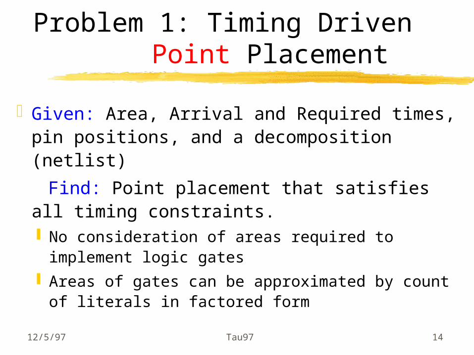
Problem 1: Timing Driven Point Placement
Given: Area, Arrival and Required times, pin positions, and a decomposition (netlist)
Find: Point placement that satisfies all timing constraints. No consideration of areas required to
implement logic gates Areas of gates can be approximated by count
of literals in factored form
12/5/97 Tau97 15
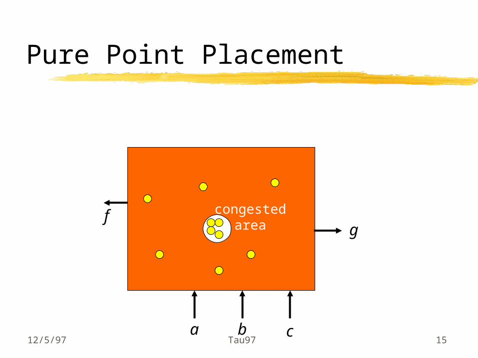
Pure Point Placement
congestedarea
a b c
fg
12/5/97 Tau97 16
Problem 2: Placement with Area Constraints
Areas are flexible. Leaf cell “gates” remain to be built. Gates types remain to be determined (PLAs, domino, PTL, etc.)
Three experimental “wireplanning ” approaches slicing
programming
matching
12/5/97 Tau97 17
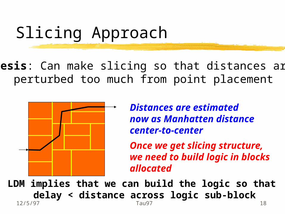
Slicing Approach
Use simulated annealing to get point placement cost function for SA is derived by doing
a delay trace through the placed pointsAfter SA, derive slicing structure
from point placement Use flexibility of areas for final
placement
12/5/97 Tau97 18
Slicing Approach
Hypothesis: Can make slicing so that distances are not perturbed too much from point placement
Distances are estimatednow as Manhatten distancecenter-to-center
Once we get slicing structure, we need to build logic in blocks allocated
LDM implies that we can build the logic so that delay < distance across logic sub-block
12/5/97 Tau97 19
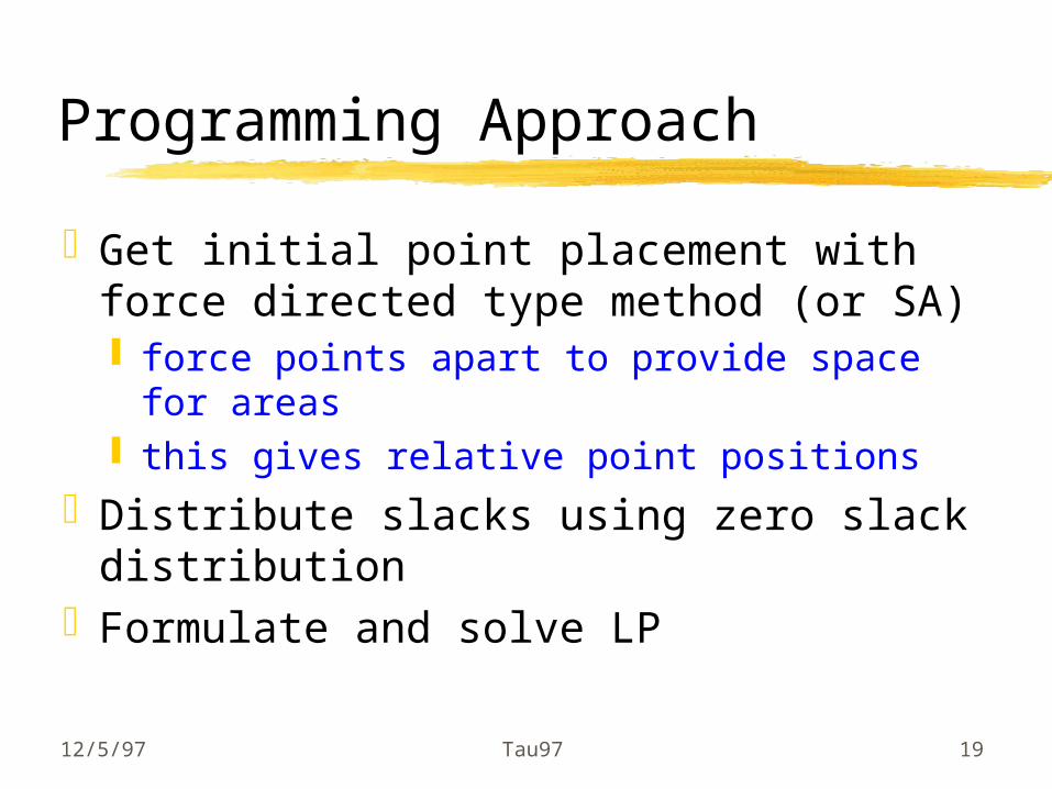
Programming Approach
Get initial point placement with force directed type method (or SA) force points apart to provide space for
areas this gives relative point positions
Distribute slacks using zero slack distribution
Formulate and solve LP
12/5/97 Tau97 20
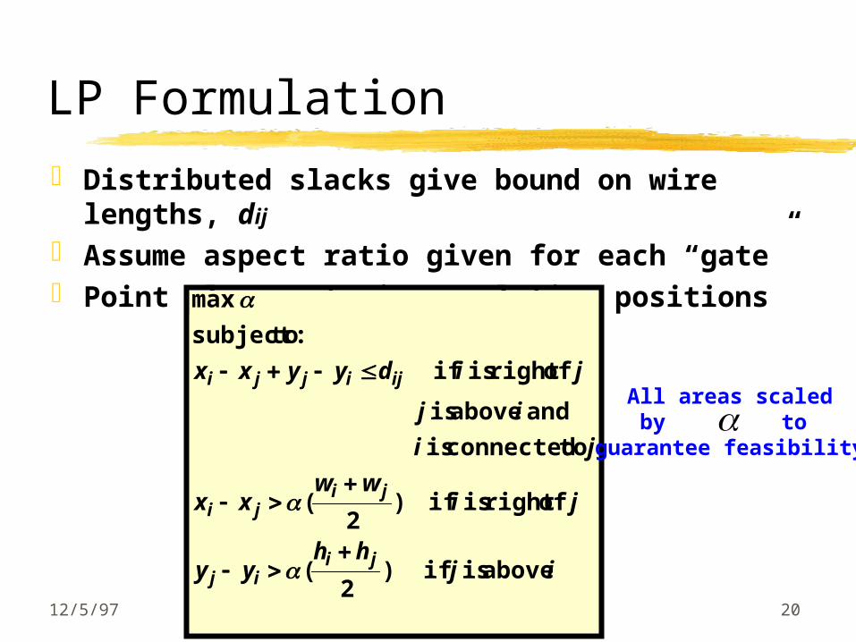
LP Formulation
Distributed slacks give bound on wire lengths, dij
Assume aspect ratio given for each “gate” Point placement gives relative positions
above is if )2
(
ofright is if )2
(
to connected is
and above is
ofright is if
:tosubject
max
ijhh
yy
jiww
xx
ji
ij
jidyyxx
jiij
jiji
ijijji
All areas scaledby to
guarantee feasibility
12/5/97 Tau97 21
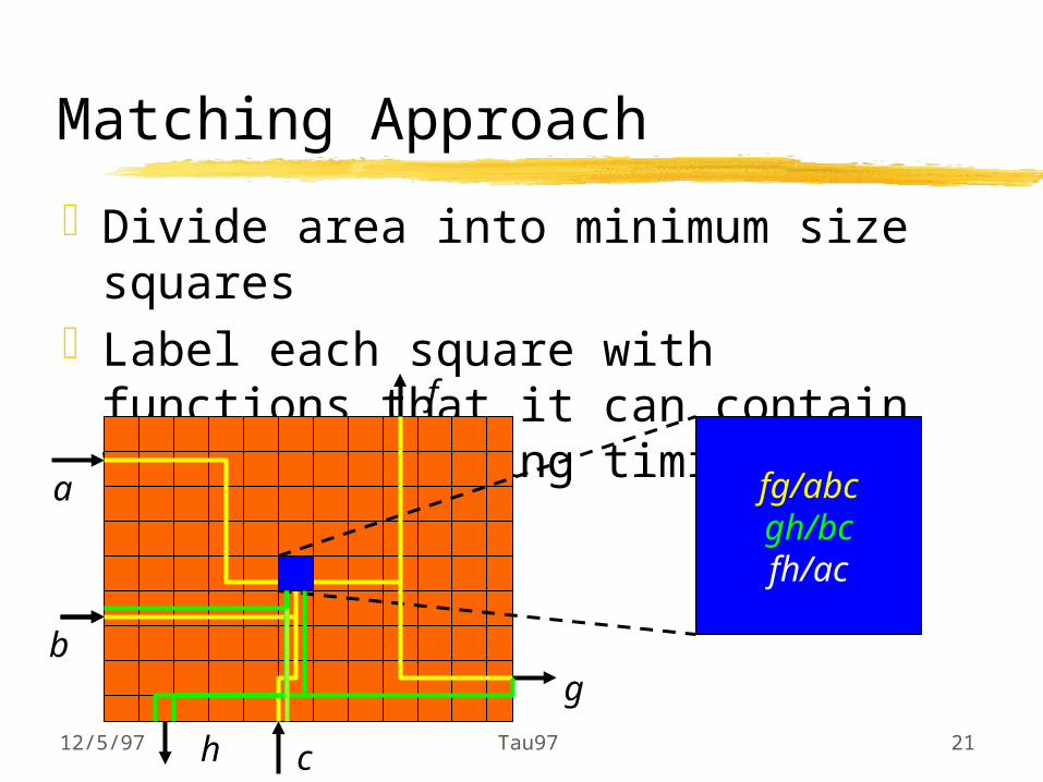
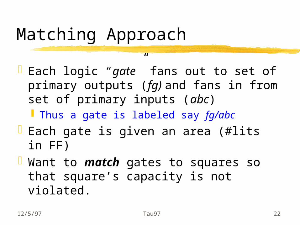
Matching Approach
Divide area into minimum size squares
Label each square with functions that it can contain without violating timing
fg/abcgh/bcfh/ac
f
g
a
b
ch
12/5/97 Tau97 22
Matching Approach
Each logic “gate” fans out to set of primary outputs (fg) and fans in from set of primary inputs (abc) Thus a gate is labeled say fg/abc
Each gate is given an area (#lits in FF)Want to match gates to squares so
that square’s capacity is not violated.
12/5/97 Tau97 23
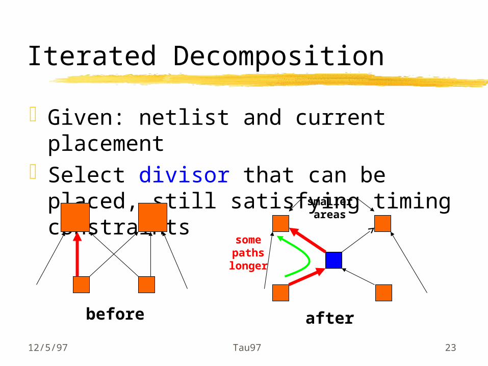
Iterated Decomposition
Given: netlist and current placementSelect divisor that can be placed, still
satisfying timing constraints
after
smallerareas
somepathslonger
before
12/5/97 Tau97 24
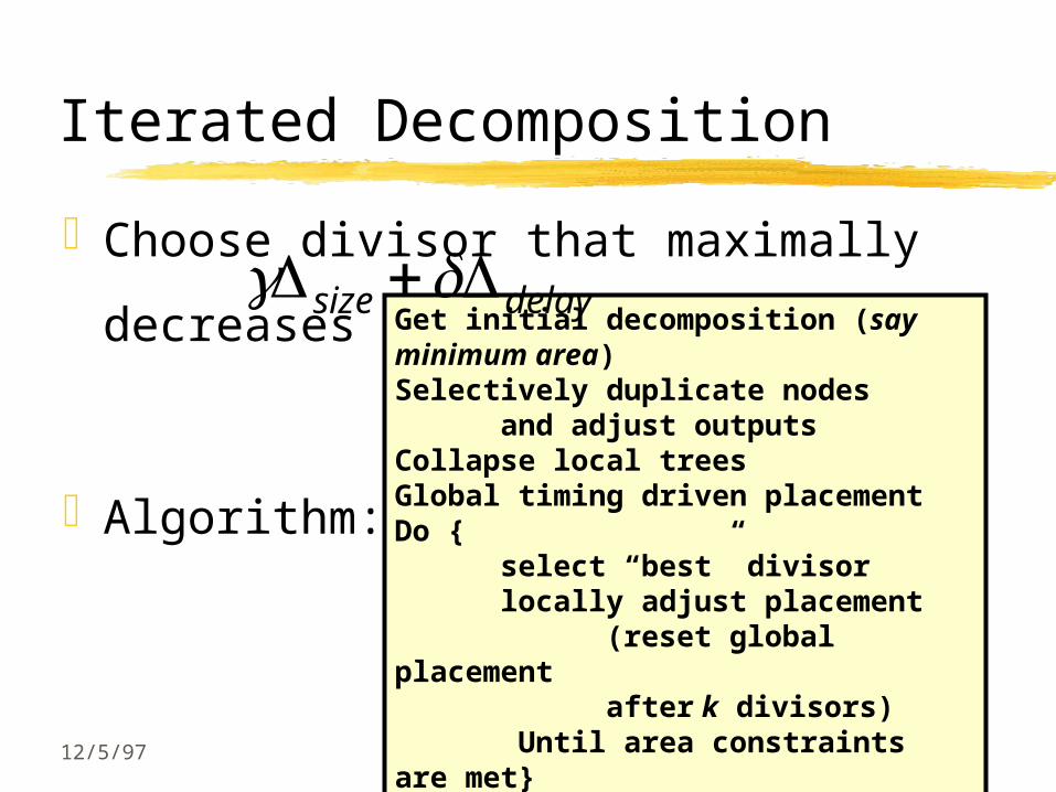
Iterated Decomposition
Choose divisor that maximally
decreases
Algorithm:
Get initial decomposition (say minimum area)Selectively duplicate nodes
and adjust outputsCollapse local treesGlobal timing driven placementDo {
select “best” divisorlocally adjust placement
(reset global placement after k divisors)
Until area constraints are met}
delaysize
12/5/97 Tau97 25
Fast Local Adjustment
With slicing method, can insert new divisor into slicing structure, get new placement and do delay trace efficiently. So we can accurately reflect area change
as it affects delayWith LP method, can also solve fast.
Just need inequalities where areas may overlap
12/5/97 Tau97 26
CommentsAfter k divisors selected and placed, re-do
global placement to better reflect all divisors i.e. do total timing driven placement on new
netlistSelective duplication and collapsing can be
done to improve timing during the iteration. experimenting with how to choose this
selective collapsing
12/5/97 Tau97 27
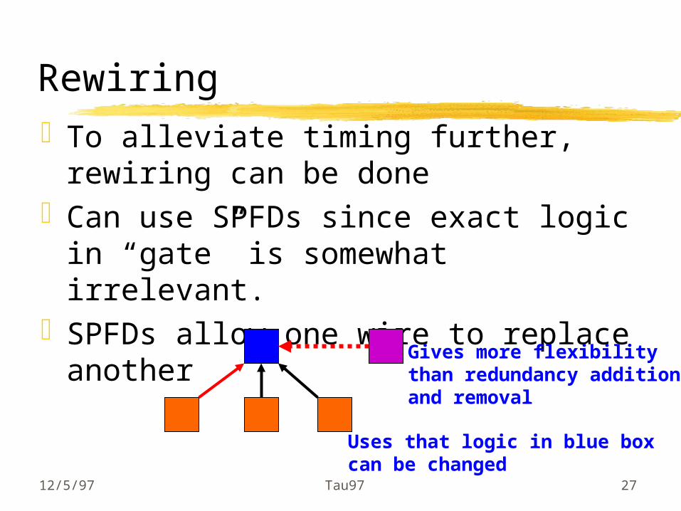
RewiringTo alleviate timing further, rewiring
can be doneCan use SPFDs since exact logic in
“gate” is somewhat irrelevant. SPFDs allow one wire to replace
anotherGives more flexibilitythan redundancy additionand removal
Uses that logic in blue boxcan be changed
12/5/97 Tau97 28
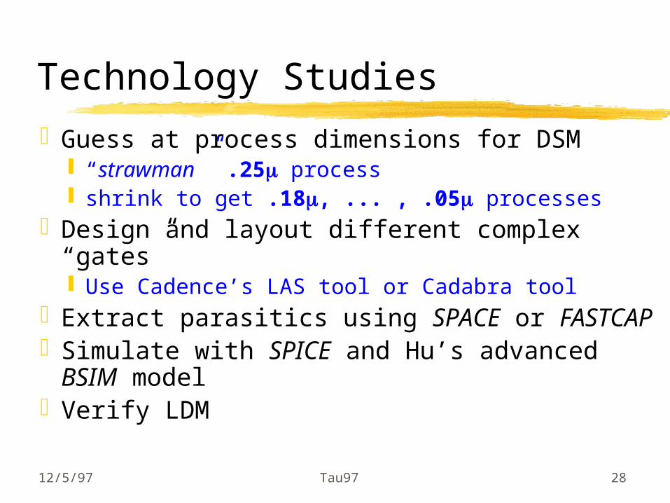
Technology Studies
Guess at process dimensions for DSM “strawman ” .25 process shrink to get .18, ... , .05 processes
Design and layout different complex “gates” Use Cadence’s LAS tool or Cadabra tool
Extract parasitics using SPACE or FASTCAPSimulate with SPICE and Hu’s advanced
BSIM modelVerify LDM
12/5/97 Tau97 29
H/W = 2.5/2.0
H/W = 2.4/1.2
H/W = 1.6/0.8
H/W = 0.6/0.3
H/W = 0.14/0.07
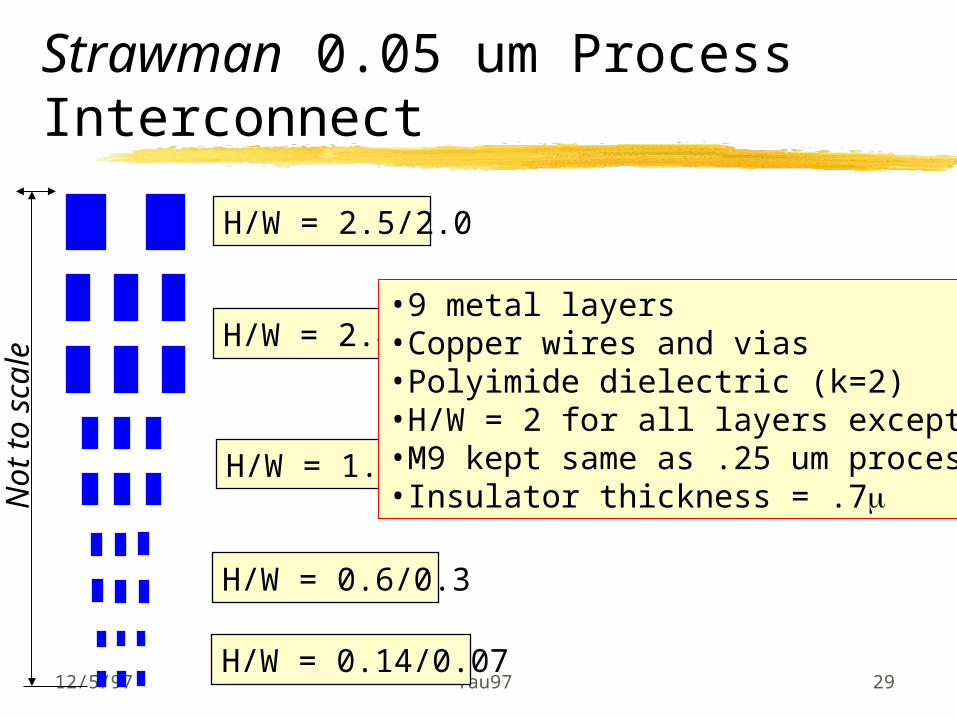
Strawman 0.05 um Process Interconnect
•9 metal layers•Copper wires and vias•Polyimide dielectric (k=2)•H/W = 2 for all layers except M9•M9 kept same as .25 um process•Insulator thickness = .7N
ot
to s
cale
12/5/97 Tau97 30
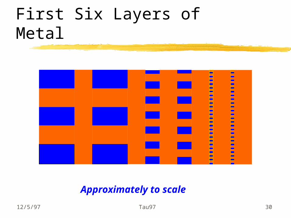
First Six Layers of Metal
Approximately to scale
12/5/97 Tau97 31
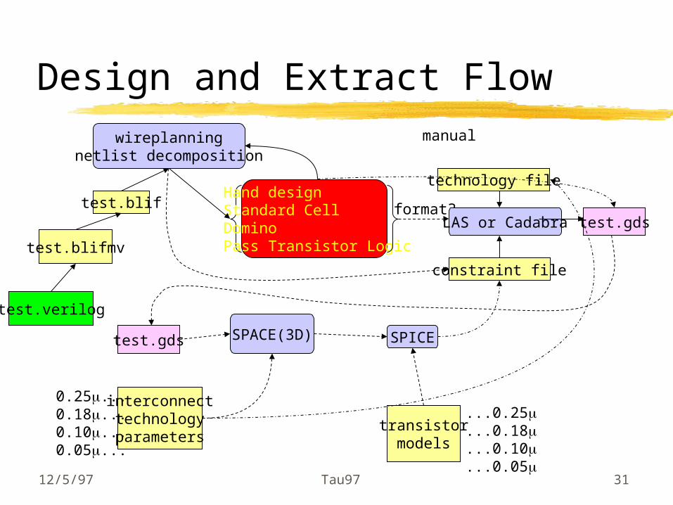
Design and Extract Flow
test.blif
wireplanningnetlist decomposition
Hand designStandard CellDominoPass Transistor Logic
technology file
format?LAS or Cadabra
test.verilog
test.blifmv
constraint file
test.gds
test.gds SPACE(3D) SPICE
interconnecttechnologyparameters
transistormodels
0.25...0.18...0.10...0.05...
...0.25
...0.18
...0.10
...0.05
manual
12/5/97 Tau97 32
Acknowledgements
Richard NewtonAlberto SangiovanniRalph OttenWilsin GostiAmit NarayanPhilip ChongMukul PrasadAmit Mehrotra
Sunil Khatri Ravi GunturiSubarna SinhaHiroshi MurataIBM, Motorola,
Intel, Fujitsu, Cadence
SRC