Embed Size (px)
Citation preview
www.nmletters.org
Titania Nanostructures for Dye-sensitized Solar
Cells
M. Malekshahi Byranvand1,∗, A. Nemati Kharat1, M. H. Bazargan2
(Received 7 December 2012; accepted 28 November 2012; published online 30 December 2012)
Abstract: Titania is one kind of important materials, which has been extensively investigated because of its
unique electronic and optical properties. Research efforts have largely focused on the optimization of the dye,
but recently the titania nanostructures electrode itself has attracted more attention. It has been shown that
particle size, shape, crystallinity, surface morphology, and chemistry of the TiO2 material are key parameters
which should be controlled for optimized performance of the solar cell. Titania can be found in different shape of
nanostructures including mesoporous, nanotube, nanowire, and nanorod structures. The present article reviews
the structural, synthesis, electronic, and optical properties of TiO2 nanostructures for dye sensitized solar cells.
Keywords: Titania nanostructures; Dye sensitized solar cells; Mesoporous; Nanotubes; Nanowires; Nanorods
Citation: M. Malekshahi Byranvand, A. Nemati Kharat and M. H. Bazargan, “Titania Nanostructures for
Dye-sensitized Solar Cells”, Nano-Micro Lett. 4 (4), 253-266 (2012). http://dx.doi.org/10.3786/nml.v4i4.
p253-266
Introduction
The world demand for clean and cheap energy fromsustainable sources is requiring important research ef-forts in diverse areas, including electricity production,storage and distribution. Since the discovery of thephotovoltaic effect in 1839 by Alexandre-Edmond Bec-querel, research has been increased in this field, partic-ularly during the last 20 years when the need for renew-able energy sources has become more critical [1]. Thecommercialized crystalline silicon-based solar cells arenow reaching energy conversion efficiency around 25%[2]. Other materials and technologies are being devel-oped to achieve lower costs and more flexibility. Amongthe promising low-cost solar cells, dye-sensitized solarcells (DSC) are under active scrutiny [1].
A breakthrough in the efficiency was reported in 1991[3]. Based on a film of nanostructured titanium diox-ide (TiO2) sensitized with a ruthenium complex and onan organic electrolyte, an energy conversion efficiencyabout 7.5% was achieved under simulated solar light
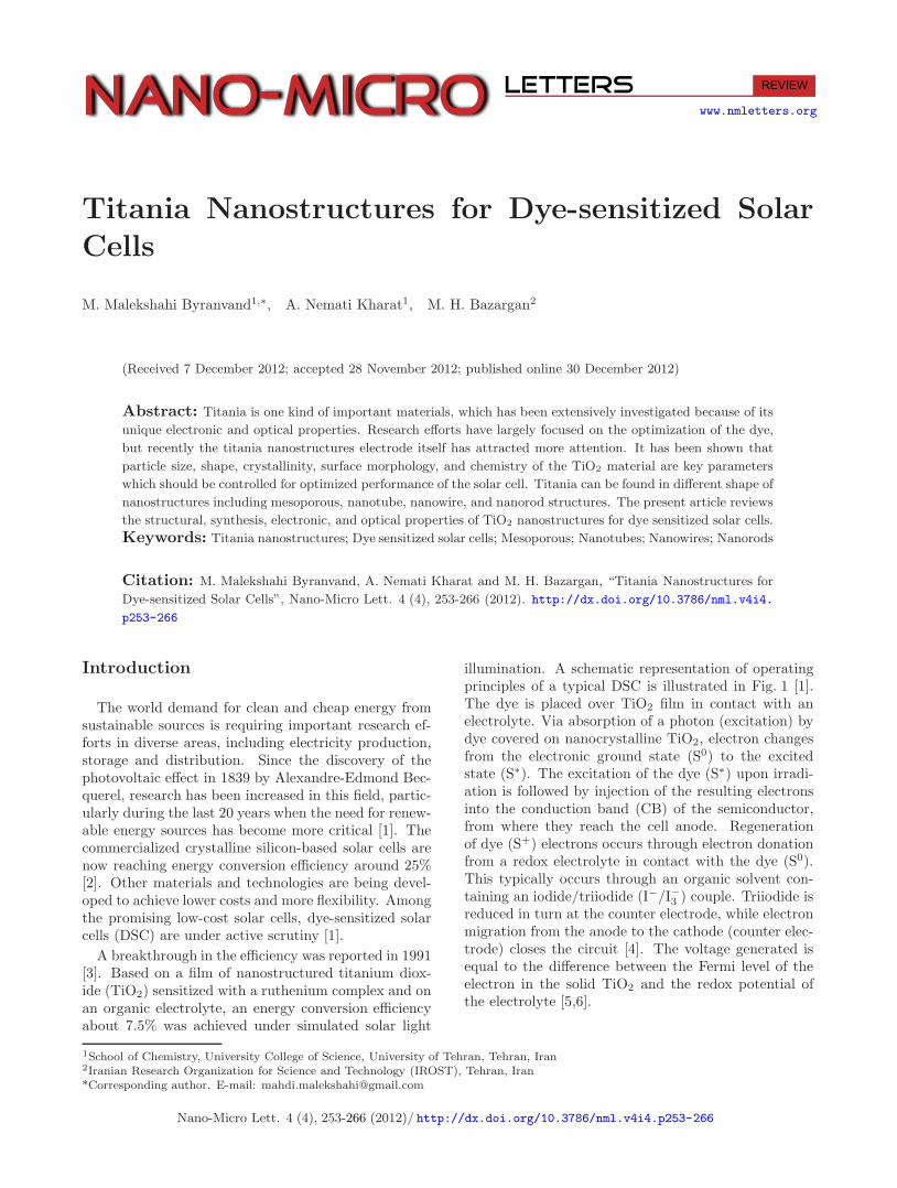
illumination. A schematic representation of operatingprinciples of a typical DSC is illustrated in Fig. 1 [1].The dye is placed over TiO2 film in contact with anelectrolyte. Via absorption of a photon (excitation) bydye covered on nanocrystalline TiO2, electron changesfrom the electronic ground state (S0) to the excitedstate (S∗). The excitation of the dye (S∗) upon irradi-ation is followed by injection of the resulting electronsinto the conduction band (CB) of the semiconductor,from where they reach the cell anode. Regenerationof dye (S+) electrons occurs through electron donationfrom a redox electrolyte in contact with the dye (S0).This typically occurs through an organic solvent con-taining an iodide/triiodide (I−/I−3 ) couple. Triiodide isreduced in turn at the counter electrode, while electronmigration from the anode to the cathode (counter elec-trode) closes the circuit [4]. The voltage generated isequal to the difference between the Fermi level of theelectron in the solid TiO2 and the redox potential ofthe electrolyte [5,6].
1School of Chemistry, University College of Science, University of Tehran, Tehran, Iran2Iranian Research Organization for Science and Technology (IROST), Tehran, Iran*Corresponding author. E-mail: [email protected]
Nano-Micro Lett. 4 (4), 253-266 (2012)/ http://dx.doi.org/10.3786/nml.v4i4.p253-266
Nano-Micro Lett. 4 (4), 253-266 (2012)/ http://dx.doi.org/10.3786/nml.v4i4.p253-266
red ox
S°/S+
e-
e-
e-
Load
S*
ElectrolyteCathodeDyeConducting glass
injection
hν
TiO2
Fig. 1 Schematic diagram of the DSC.
Since that breakthrough, research has been growingexponentially in order to increase the efficiency or thestability of dye sensitized solar cells through the opti-mization of their components. Among others, a fac-tor was responsible for this significant progress: theuse of nanostructured TiO2, providing a large surfacearea and thus allowing a larger amount of dye to beattached to the TiO2 surface [7,8]. A high performance
DSC requires the TiO2 film with proper small particlesize and mesoporosity so that a large amount of dye canbe adsorbed for achieving high photoelectric conversionefficiency in DSC [9].
TiO2 exists in three mineral forms: anatase, rutileand brookite [10]. Anatase type TiO2 has a crys-talline structure that corresponds to the tetragonal sys-tem (with dipyramidal habit) and is used mainly as aphotocatalyst under UV irradiation. Rutile type TiO2
also has a tetragonal crystal structure (with prismatichabit). This type of titania is mainly used as white pig-ment in paint. Brookite type TiO2 has an orthorhom-bic crystalline structure. In general, TiO2 is preferredin anatase and rutile form because of its high specificarea, non-toxic, photochemically stable and relativelyin-expensive [11-13].
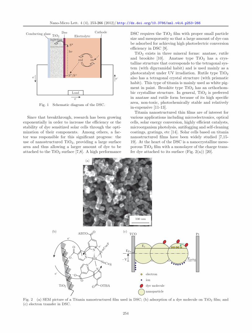
Titania nanostructured thin films are of interest forvarious applications including microelectronics, opticalcells, solar energy conversion, highly efficient catalysts,microorganism photolysis, antifogging and self-cleaningcoatings, gratings, etc [14]. Solar cells based on titaniananostructured films have been widely studied [7,15-19]. At the heart of the DSC is a nanocrystalline meso-porous TiO2 film with a monolayer of the charge trans-fer dye attached to its surface (Fig. 2(a)) [20].
ABTO O
S
TCO
100 nm
(a)
(b) (c)
−V
Pt
CO
NN
N
NN
OTBAO
O
−O
O−
H+
H+
N C S
electron
ion
dye molecule
nanoparticle
RH
Ec
EFn
TiO2
Eredox
e-
e-
e-
100 nm
(a)
Fig. 2 (a) SEM picture of a Titania nanostructured film used in DSC; (b) adsorption of a dye molecule on TiO2 film; and(c) electron transfer in DSC.
254
Nano-Micro Lett. 4 (4), 253-266 (2012)/ http://dx.doi.org/10.3786/nml.v4i4.p253-266
Photoexcitation of the dye injects an electron intothe conduction band of TiO2 (Fig. 2(b)) [20]. The elec-tron can be conducted to the outer circuit to drive theload and make electric power. The original state ofthe dye is subsequently restored by electron donationfrom the electrolyte, usually an organic solvent con-taining a redox system, such as the iodide/triiodidecouple. The regeneration of the sensitizer by iodideprevents the recapture of the conduction band electronby the oxidized dye. The iodide is regenerated in turnby the reduction of triiodide at the counter electrode,with the circuit being completed via electron migrationthrough the external load. The voltage generated underillumination corresponds to the difference between theFermi level of TiO2 and the redox potential of the elec-trolyte (Fig. 2(c)) [20]. Overall, the device generateselectric power from light without suffering any perma-nent chemical transformation [7,15-19].
The oxide material of choice for many of these sys-tems has been TiO2 [21-23]. Its properties are in-timately depended to the material content, chemicalcomposition, structure and surface morphology. Fortu-nately colloid chemistry has greatly developed in thelast two decades. It is now possible to control theprocessing parameters such as precursor chemistry, hy-drothermal growth temperature, binder addition andsintering conditions and optimize the key parametersof the film, namely, porosity, pore size distribution,light scattering, electron percolation. On the mate-rial content and morphology, two crystalline forms ofanatase and rutile for TiO2 are important (the thirdform brookite is difficult to obtain). Anatase is thelow temperature stable form and gives mesoscopic filmsthat are transparent and colorless. The predominantmorphology of the particles is bipyramidal exposingwell-developed (101) faces [24].
Titania has been observed mainly in different formsof nanostructures such as mesoporous [25], nanotube[26], nanowire [27] and nanorod [28] structures. Thestructural, synthesis, electronic and optical propertiesof TiO2 nanomaterials for DSC are reviewed in the nextsection.
In this review, we focus on some of the developmentsof titania nanostructures for applications in DSC. In ad-dition we summarize the synthesis pathways and mor-phology of the nanostructured titanium dioxide.
Mesoporous TiO2 films
Preparation of mesoporous TiO2 films consists of twosteps: first, a colloidal solution containing nanosizedparticles of the oxide is formed which is used subse-quently to produce a few micron thick films with good
electrical conduction properties [20,24]. In a typicalsynthesis process, a nanocrystalline TiO2 film involvescontrolled hydrolysis of a Ti (IV) salt, usually an alkox-ide such as Ti-isopropoxide or a chloride followed bypeptization [5]. In order to obtain particles of desiredsize, the hydrolysis and condensation kinetics must becontrolled. Ti-alkoxides with bulky groups such asbutoxide hydrolyze slowly allowing slow condensationrates. Autoclaving of these sols (heating at 200∼250℃
for 12 h) allows controlled growth of the primary par-ticles and also to some extent, the crystallinity [24].
During this hydrothermal growth smaller particlesdissolve and fuse to large particles by a process knownas ‘Ostwald ripening’. After removal of solvent and ad-dition of a binder the sol is now ready for deposition onthe substrate. For the latter, a conducting glass sheetis often used and the sol is deposited by doctor bladingor screen printing and fired in air for sintering. Thefilm thickness is typically 1∼20 µm and the film massapproximately 1∼2 mg/cm2. Analysis of the porousfilms shows the porosity to be approximately 50% (theaverage pore size being 15 nm).
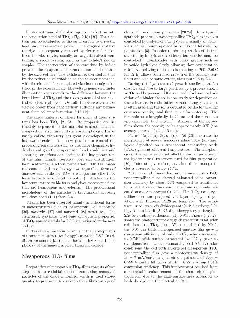
Figure 3(a), 3(b), 3(c), 3(d), 3(e) [20] illustrate themorphology of several nanocrystalline TiO2 (anatase)layers deposited on a transparent conducting oxide(TCO) glass at different temperatures. The morphol-ogy of the particles is controlled by the temperature ofthe hydrothermal treatment used for film preparation[20]. Interestingly, self-organization of the nanoparti-cles is observed at below 240℃.
Zukalova et al. found that ordered mesoporous TiO2
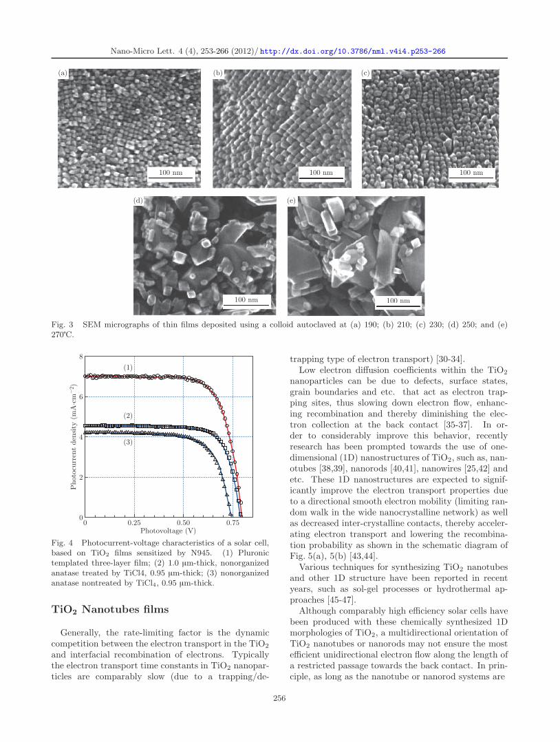
nanocrystalline films showed enhanced solar conver-sion efficiency by about 50% compared to traditionalfilms of the same thickness made from randomly ori-ented anatase nanocrystals [29]. The TiO2 nanocrys-talline film was prepared via layer- by-layer depo-sition with Pluronic P123 as template. The sensi-tizer used was cis-dithiocyanato(4,4′-dicarboxy-2,2′-bipyridine)(4,4′-di-(2-(3,6-dimethoxyphenyl)ethenyl)-2,2′-bi-pyridine) ruthenium (II), N945. Figure 4 [23,29]shows the photocurrent-voltage characteristics for solarcells based on TiO2 films. When sensitized by N945,the 0.95 µm thick nonorganized anatase film gave aconversion efficiency of only 2.21%, which increasedto 2.74% with surface treatment by TiCl4 prior todye deposition. Under standard global AM 1.5 solarconditions, the cell with an ordered mesoporous TiO2
nanocrystalline film gave a photocurrent density ofIP = 7 mA/cm2, an open circuit potential of VOC =0.799 V, and a fill factor of FF = 0.72, yielding 4.04%conversion efficiency. This improvement resulted froma remarkable enhancement of the short circuit pho-tocurrent, due to the huge surface area accessible toboth the dye and the electrolyte [29].
255
Nano-Micro Lett. 4 (4), 253-266 (2012)/ http://dx.doi.org/10.3786/nml.v4i4.p253-266
(a) (b) (c)
(d) (e)
100 nm 100 nm
100 nm100 nm100 nm
(a) (b) (c)
(d) (e)
100 nm 100 nm
100 nm100 nm100 nm
Fig. 3 SEM micrographs of thin films deposited using a colloid autoclaved at (a) 190; (b) 210; (c) 230; (d) 250; and (e)270℃.
(1)
(2)
(3)
8
6
4
2
00 0.25 0.50 0.75
Photovoltage (V)
Phot
ocurr
ent
den
sity
(m
A·c
m−
2 )
Fig. 4 Photocurrent-voltage characteristics of a solar cell,based on TiO2 films sensitized by N945. (1) Pluronictemplated three-layer film; (2) 1.0 µm-thick, nonorganizedanatase treated by TiCl4, 0.95 µm-thick; (3) nonorganizedanatase nontreated by TiCl4, 0.95 µm-thick.
TiO2 Nanotubes films
Generally, the rate-limiting factor is the dynamiccompetition between the electron transport in the TiO2
and interfacial recombination of electrons. Typicallythe electron transport time constants in TiO2 nanopar-ticles are comparably slow (due to a trapping/de-
trapping type of electron transport) [30-34].Low electron diffusion coefficients within the TiO2
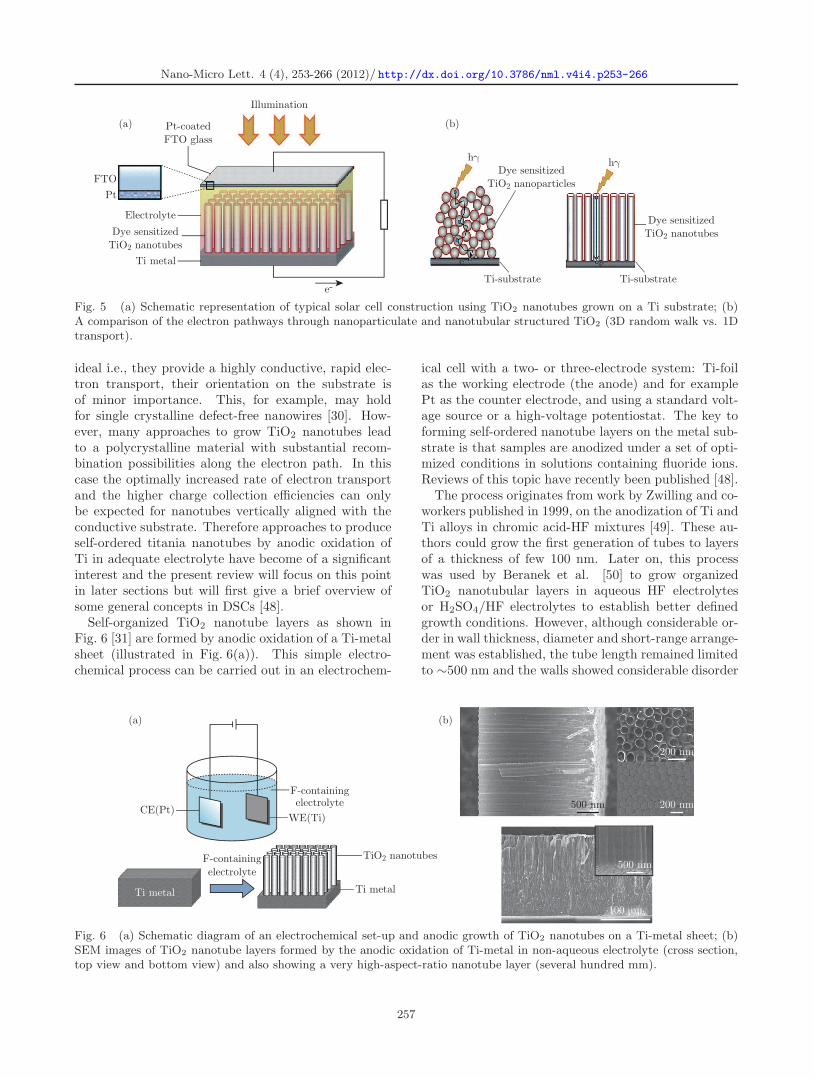
nanoparticles can be due to defects, surface states,grain boundaries and etc. that act as electron trap-ping sites, thus slowing down electron flow, enhanc-ing recombination and thereby diminishing the elec-tron collection at the back contact [35-37]. In or-der to considerably improve this behavior, recentlyresearch has been prompted towards the use of one-dimensional (1D) nanostructures of TiO2, such as, nan-otubes [38,39], nanorods [40,41], nanowires [25,42] andetc. These 1D nanostructures are expected to signif-icantly improve the electron transport properties dueto a directional smooth electron mobility (limiting ran-dom walk in the wide nanocrystalline network) as wellas decreased inter-crystalline contacts, thereby acceler-ating electron transport and lowering the recombina-tion probability as shown in the schematic diagram ofFig. 5(a), 5(b) [43,44].
Various techniques for synthesizing TiO2 nanotubesand other 1D structure have been reported in recentyears, such as sol-gel processes or hydrothermal ap-proaches [45-47].
Although comparably high efficiency solar cells havebeen produced with these chemically synthesized 1Dmorphologies of TiO2, a multidirectional orientation ofTiO2 nanotubes or nanorods may not ensure the mostefficient unidirectional electron flow along the length ofa restricted passage towards the back contact. In prin-ciple, as long as the nanotube or nanorod systems are
256
Nano-Micro Lett. 4 (4), 253-266 (2012)/ http://dx.doi.org/10.3786/nml.v4i4.p253-266
e-
e-
hγ hγDye sensitized
TiO2 nanoparticles
Illumination
(a) (b)Pt-coatedFTO glass
FTO
Pt
Electrolyte
Ti metal
Dye sensitizedTiO2 nanotubesDye sensitized
TiO2 nanotubes
Ti-substrate
e-
Ti-substrate
Fig. 5 (a) Schematic representation of typical solar cell construction using TiO2 nanotubes grown on a Ti substrate; (b)A comparison of the electron pathways through nanoparticulate and nanotubular structured TiO2 (3D random walk vs. 1Dtransport).
ideal i.e., they provide a highly conductive, rapid elec-tron transport, their orientation on the substrate isof minor importance. This, for example, may holdfor single crystalline defect-free nanowires [30]. How-ever, many approaches to grow TiO2 nanotubes leadto a polycrystalline material with substantial recom-bination possibilities along the electron path. In thiscase the optimally increased rate of electron transportand the higher charge collection efficiencies can onlybe expected for nanotubes vertically aligned with theconductive substrate. Therefore approaches to produceself-ordered titania nanotubes by anodic oxidation ofTi in adequate electrolyte have become of a significantinterest and the present review will focus on this pointin later sections but will first give a brief overview ofsome general concepts in DSCs [48].
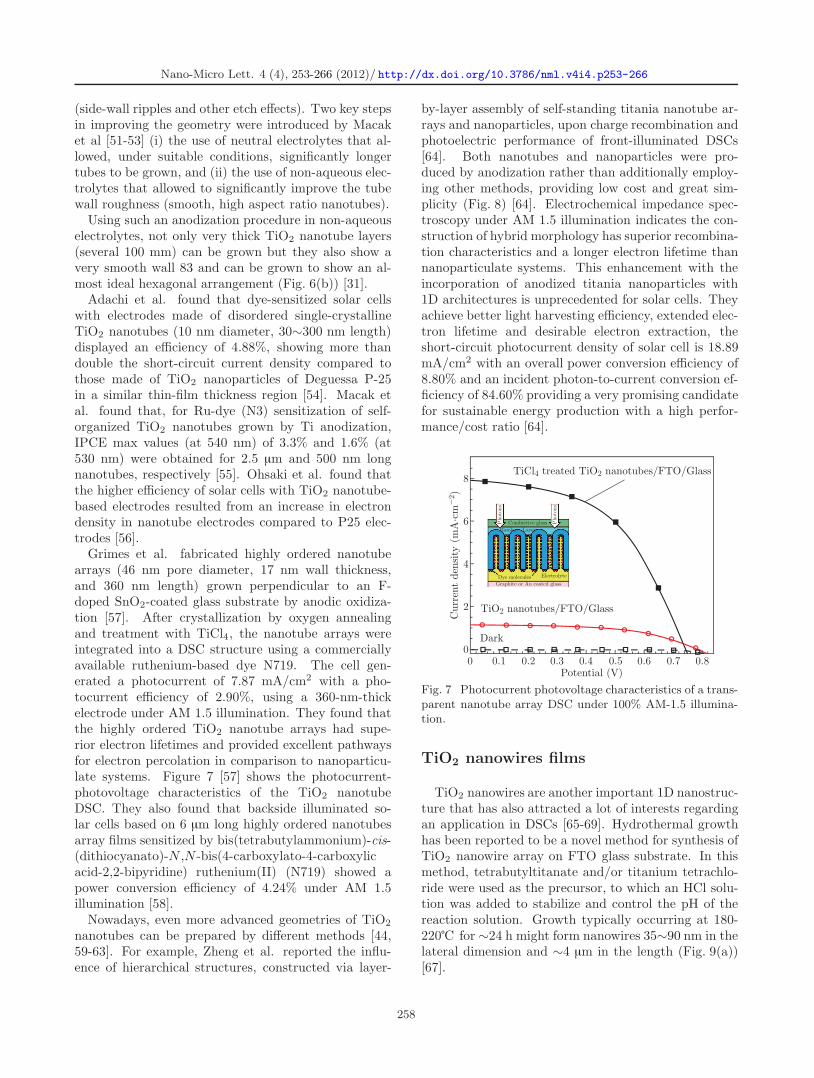
Self-organized TiO2 nanotube layers as shown inFig. 6 [31] are formed by anodic oxidation of a Ti-metalsheet (illustrated in Fig. 6(a)). This simple electro-chemical process can be carried out in an electrochem-
ical cell with a two- or three-electrode system: Ti-foilas the working electrode (the anode) and for examplePt as the counter electrode, and using a standard volt-age source or a high-voltage potentiostat. The key toforming self-ordered nanotube layers on the metal sub-strate is that samples are anodized under a set of opti-mized conditions in solutions containing fluoride ions.Reviews of this topic have recently been published [48].
The process originates from work by Zwilling and co-workers published in 1999, on the anodization of Ti andTi alloys in chromic acid-HF mixtures [49]. These au-thors could grow the first generation of tubes to layersof a thickness of few 100 nm. Later on, this processwas used by Beranek et al. [50] to grow organizedTiO2 nanotubular layers in aqueous HF electrolytesor H2SO4/HF electrolytes to establish better definedgrowth conditions. However, although considerable or-der in wall thickness, diameter and short-range arrange-ment was established, the tube length remained limitedto ∼500 nm and the walls showed considerable disorder
CE(Pt)
Ti metal Ti metal
F-containingelectrolyte
TiO2 nanotubes
WE(Ti)
F-containingelectrolyte
(b)(a)
500 nm 200 nm
500 nm
100 µm
200 nm
Fig. 6 (a) Schematic diagram of an electrochemical set-up and anodic growth of TiO2 nanotubes on a Ti-metal sheet; (b)SEM images of TiO2 nanotube layers formed by the anodic oxidation of Ti-metal in non-aqueous electrolyte (cross section,top view and bottom view) and also showing a very high-aspect-ratio nanotube layer (several hundred mm).
257
Nano-Micro Lett. 4 (4), 253-266 (2012)/ http://dx.doi.org/10.3786/nml.v4i4.p253-266
(side-wall ripples and other etch effects). Two key stepsin improving the geometry were introduced by Macaket al [51-53] (i) the use of neutral electrolytes that al-lowed, under suitable conditions, significantly longertubes to be grown, and (ii) the use of non-aqueous elec-trolytes that allowed to significantly improve the tubewall roughness (smooth, high aspect ratio nanotubes).
Using such an anodization procedure in non-aqueouselectrolytes, not only very thick TiO2 nanotube layers(several 100 mm) can be grown but they also show avery smooth wall 83 and can be grown to show an al-most ideal hexagonal arrangement (Fig. 6(b)) [31].
Adachi et al. found that dye-sensitized solar cellswith electrodes made of disordered single-crystallineTiO2 nanotubes (10 nm diameter, 30∼300 nm length)displayed an efficiency of 4.88%, showing more thandouble the short-circuit current density compared tothose made of TiO2 nanoparticles of Deguessa P-25in a similar thin-film thickness region [54]. Macak etal. found that, for Ru-dye (N3) sensitization of self-organized TiO2 nanotubes grown by Ti anodization,IPCE max values (at 540 nm) of 3.3% and 1.6% (at530 nm) were obtained for 2.5 µm and 500 nm longnanotubes, respectively [55]. Ohsaki et al. found thatthe higher efficiency of solar cells with TiO2 nanotube-based electrodes resulted from an increase in electrondensity in nanotube electrodes compared to P25 elec-trodes [56].
Grimes et al. fabricated highly ordered nanotubearrays (46 nm pore diameter, 17 nm wall thickness,and 360 nm length) grown perpendicular to an F-doped SnO2-coated glass substrate by anodic oxidiza-tion [57]. After crystallization by oxygen annealingand treatment with TiCl4, the nanotube arrays wereintegrated into a DSC structure using a commerciallyavailable ruthenium-based dye N719. The cell gen-erated a photocurrent of 7.87 mA/cm2 with a pho-tocurrent efficiency of 2.90%, using a 360-nm-thickelectrode under AM 1.5 illumination. They found thatthe highly ordered TiO2 nanotube arrays had supe-rior electron lifetimes and provided excellent pathwaysfor electron percolation in comparison to nanoparticu-late systems. Figure 7 [57] shows the photocurrent-photovoltage characteristics of the TiO2 nanotubeDSC. They also found that backside illuminated so-lar cells based on 6 µm long highly ordered nanotubesarray films sensitized by bis(tetrabutylammonium)-cis-(dithiocyanato)-N ,N -bis(4-carboxylato-4-carboxylicacid-2,2-bipyridine) ruthenium(II) (N719) showed apower conversion efficiency of 4.24% under AM 1.5illumination [58].
Nowadays, even more advanced geometries of TiO2
nanotubes can be prepared by different methods [44,59-63]. For example, Zheng et al. reported the influ-ence of hierarchical structures, constructed via layer-
by-layer assembly of self-standing titania nanotube ar-rays and nanoparticles, upon charge recombination andphotoelectric performance of front-illuminated DSCs[64]. Both nanotubes and nanoparticles were pro-duced by anodization rather than additionally employ-ing other methods, providing low cost and great sim-plicity (Fig. 8) [64]. Electrochemical impedance spec-troscopy under AM 1.5 illumination indicates the con-struction of hybrid morphology has superior recombina-tion characteristics and a longer electron lifetime thannanoparticulate systems. This enhancement with theincorporation of anodized titania nanoparticles with1D architectures is unprecedented for solar cells. Theyachieve better light harvesting efficiency, extended elec-tron lifetime and desirable electron extraction, theshort-circuit photocurrent density of solar cell is 18.89mA/cm2 with an overall power conversion efficiency of8.80% and an incident photon-to-current conversion ef-ficiency of 84.60% providing a very promising candidatefor sustainable energy production with a high perfor-mance/cost ratio [64].
TiCl4 treated TiO2 nanotubes/FTO/Glass
TiO2 nanotubes/FTO/Glass
Phot
ons
Conductive glass
Layer
Dye molecules Electrolyte
Graphite or Au coated glass
Bamler
Phot
ons
8
6
4
2
0Dark
0 0.1 0.2 0.3 0.4 0.5 0.6 0.7 0.8Potential (V)
Curr
ent
den
sity
(m
A·c
m−
2 )
Fig. 7 Photocurrent photovoltage characteristics of a trans-parent nanotube array DSC under 100% AM-1.5 illumina-tion.
TiO2 nanowires films
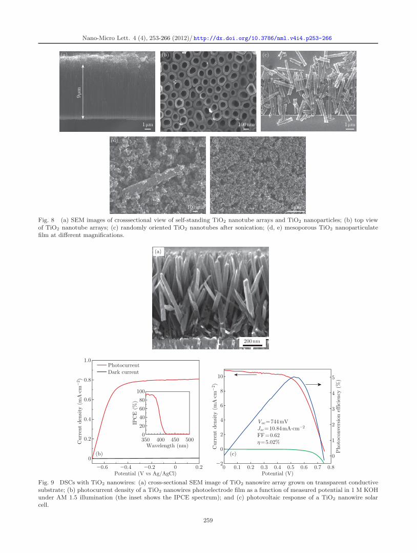
TiO2 nanowires are another important 1D nanostruc-ture that has also attracted a lot of interests regardingan application in DSCs [65-69]. Hydrothermal growthhas been reported to be a novel method for synthesis ofTiO2 nanowire array on FTO glass substrate. In thismethod, tetrabutyltitanate and/or titanium tetrachlo-ride were used as the precursor, to which an HCl solu-tion was added to stabilize and control the pH of thereaction solution. Growth typically occurring at 180-220℃ for ∼24 h might form nanowires 35∼90 nm in thelateral dimension and ∼4 µm in the length (Fig. 9(a))[67].
258
Nano-Micro Lett. 4 (4), 253-266 (2012)/ http://dx.doi.org/10.3786/nml.v4i4.p253-266
1µm 1µm
1µm100nm
(d)
(a) (b) (c)
(e)
9µm
100nm
Fig. 8 (a) SEM images of crosssectional view of self-standing TiO2 nanotube arrays and TiO2 nanoparticles; (b) top viewof TiO2 nanotube arrays; (c) randomly oriented TiO2 nanotubes after sonication; (d, e) mesoporous TiO2 nanoparticulatefilm at different magnifications.
10
8
6
4
2
0
−20 0.1 0.2 0.3 0.4 0.5 0.6 0.7 0.8
5
4
3
2
1
0
Phot
oco
nve
rsio
n e
ffic
iency
(%
)
Potential (V)Potential (V vs Ag/AgCl)
Curr
ent
den
sity
(m
A·c
m−
2 )
1.0
0.8
0.6
0.4
0.2
0
Curr
ent
den
sity
(m
A·c
m−
2 )
Voc=744mVJsc=10.84mA·cm−2
FF=0.62η=5.02%
−0.6 −0.4 −0.2 0
350
PhotocurrentDark current
100
80
60
40
20
0400 500
Wavelength (nm)
IPC
E (
%)
450
0.2
200nm
(a)
(b) (c)
200nm
(a)
Fig. 9 DSCs with TiO2 nanowires: (a) cross-sectional SEM image of TiO2 nanowire array grown on transparent conductivesubstrate; (b) photocurrent density of a TiO2 nanowires photoelectrode film as a function of measured potential in 1 M KOHunder AM 1.5 illumination (the inset shows the IPCE spectrum); and (c) photovoltaic response of a TiO2 nanowire solarcell.
259
Nano-Micro Lett. 4 (4), 253-266 (2012)/ http://dx.doi.org/10.3786/nml.v4i4.p253-266
The dependence of photocurrent density on the mea-sured potential was studied while the TiO2 nanowireswere under AM 1.5 illumination, revealing a saturatedphotocurrent at the bias of approximately −0.25 V (vsreference electrode) (Fig. 9(b)) [66]. Compared with apositive bias in the range of 0.5∼1 V needed in thenanoparticle electrode to completely separate the pho-togenerated electron-hole pairs, such a low bias indi-cated that the nanowires possessed a low series resis-tance and had more effective capability of facilely sepa-rating the photogenerated charges. This is in agreementwith what is presented in the incident photo to collectedelectron (IPCE) spectrum of TiO2 nanowires (inset ofFig. 9(b)), in which the efficiency is shown to reach amaximum of approximately 90%, implying a low chargerecombination in the nanowire/electrolyte system. Testof the solar cell performance of the TiO2 nanowireswith a standard DSC configure revealed an overall con-version efficiency of 5% (Fig. 9(c)) [66], which is obvi-ously much higher than those of 1.2∼1.5% reported forZnO nanowires even with length up to 40 µm [70,71].This more likely resulted from a better coupling ofthe nanowires of TiO2 with the ruthenium-based dyemolecules, whereas it is well-known that the ZnO lacksstability in an acid dye solution and therefore may forma Zn2+/dye complex on the surface which seriously re-tards the electron injection [67,71,72].
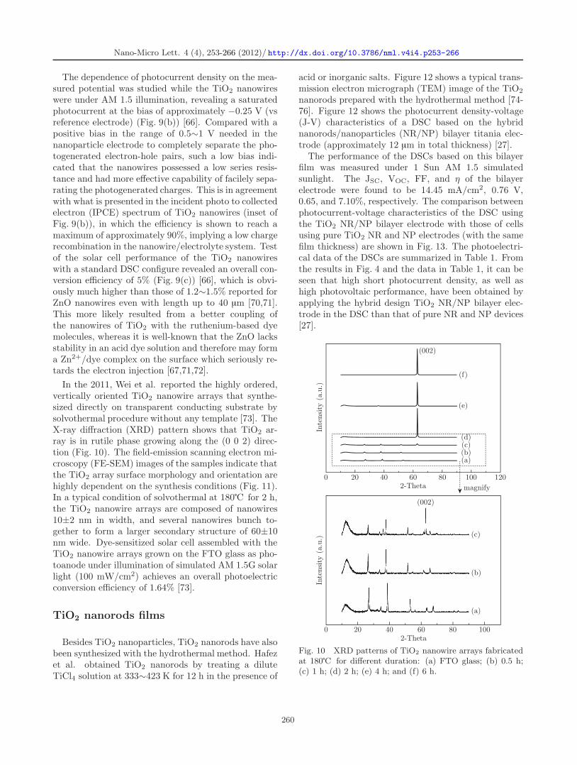
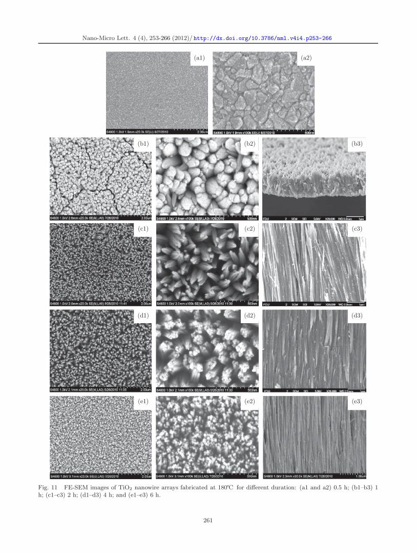
In the 2011, Wei et al. reported the highly ordered,vertically oriented TiO2 nanowire arrays that synthe-sized directly on transparent conducting substrate bysolvothermal procedure without any template [73]. TheX-ray diffraction (XRD) pattern shows that TiO2 ar-ray is in rutile phase growing along the (0 0 2) direc-tion (Fig. 10). The field-emission scanning electron mi-croscopy (FE-SEM) images of the samples indicate thatthe TiO2 array surface morphology and orientation arehighly dependent on the synthesis conditions (Fig. 11).In a typical condition of solvothermal at 180℃ for 2 h,the TiO2 nanowire arrays are composed of nanowires10±2 nm in width, and several nanowires bunch to-gether to form a larger secondary structure of 60±10nm wide. Dye-sensitized solar cell assembled with theTiO2 nanowire arrays grown on the FTO glass as pho-toanode under illumination of simulated AM 1.5G solarlight (100 mW/cm2) achieves an overall photoelectricconversion efficiency of 1.64% [73].
TiO2 nanorods films
Besides TiO2 nanoparticles, TiO2 nanorods have alsobeen synthesized with the hydrothermal method. Hafezet al. obtained TiO2 nanorods by treating a diluteTiCl4 solution at 333∼423 K for 12 h in the presence of
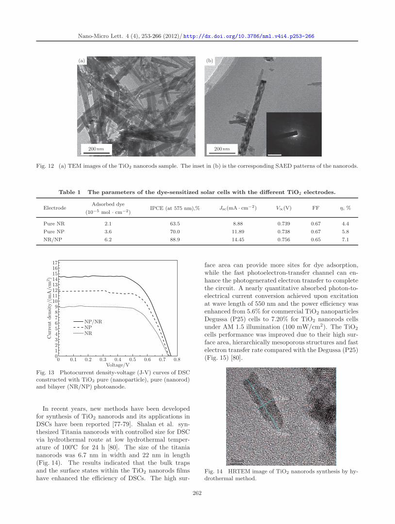
acid or inorganic salts. Figure 12 shows a typical trans-mission electron micrograph (TEM) image of the TiO2
nanorods prepared with the hydrothermal method [74-76]. Figure 12 shows the photocurrent density-voltage(J-V) characteristics of a DSC based on the hybridnanorods/nanoparticles (NR/NP) bilayer titania elec-trode (approximately 12 µm in total thickness) [27].
The performance of the DSCs based on this bilayerfilm was measured under 1 Sun AM 1.5 simulatedsunlight. The JSC, VOC, FF, and η of the bilayerelectrode were found to be 14.45 mA/cm2, 0.76 V,0.65, and 7.10%, respectively. The comparison betweenphotocurrent-voltage characteristics of the DSC usingthe TiO2 NR/NP bilayer electrode with those of cellsusing pure TiO2 NR and NP electrodes (with the samefilm thickness) are shown in Fig. 13. The photoelectri-cal data of the DSCs are summarized in Table 1. Fromthe results in Fig. 4 and the data in Table 1, it can beseen that high short photocurrent density, as well ashigh photovoltaic performance, have been obtained byapplying the hybrid design TiO2 NR/NP bilayer elec-trode in the DSC than that of pure NR and NP devices[27].
(002)
Inte
nsi
ty (
a.u.)
Inte
nsi
ty (
a.u.)
(f)
(e)
(d)(c)(b)(a)
0 20 40 602-Theta
80
magnify
100 120
0 20 40 60
(a)
(b)
(c)
(002)
2-Theta80 100
Fig. 10 XRD patterns of TiO2 nanowire arrays fabricatedat 180℃ for different duration: (a) FTO glass; (b) 0.5 h;(c) 1 h; (d) 2 h; (e) 4 h; and (f) 6 h.
260
Nano-Micro Lett. 4 (4), 253-266 (2012)/ http://dx.doi.org/10.3786/nml.v4i4.p253-266
(a1)
(b1) (b2) (b3)
(c1) (c2) (c3)
(d1) (d2) (d3)
(e1) (e2) (e3)
(a2)
Fig. 11 FE-SEM images of TiO2 nanowire arrays fabricated at 180℃ for different duration: (a1 and a2) 0.5 h; (b1–b3) 1h; (c1–c3) 2 h; (d1–d3) 4 h; and (e1–e3) 6 h.
261
Nano-Micro Lett. 4 (4), 253-266 (2012)/ http://dx.doi.org/10.3786/nml.v4i4.p253-266
200nm 200nm
(b)(a)
5nm200nm 200nm
(b)(a)
55nnmm
Fig. 12 (a) TEM images of the TiO2 nanorods sample. The inset in (b) is the corresponding SAED patterns of the nanorods.
Table 1 The parameters of the dye-sensitized solar cells with the different TiO2 electrodes.
ElectrodeAdsorbed dye
(10−5 mol · cm−2)IPCE (at 575 nm),% Jsc(mA · cm−2) V∝(V) FF η, %
Pure NR 2.1 63.5 8.88 0.739 0.67 4.4
Pure NP 3.6 70.0 11.89 0.738 0.67 5.8
NR/NP 6.2 88.9 14.45 0.756 0.65 7.1
NP/NRNPNR
Curr
ent
den
sity
/(m
A/c
m2 )
171615141312111098765432100 0.1 0.2 0.3 0.4 0.5 0.6 0.7 0.8
Voltage/V
Fig. 13 Photocurrent density-voltage (J-V) curves of DSCconstructed with TiO2 pure (nanoparticle), pure (nanorod)and bilayer (NR/NP) photoanode.
In recent years, new methods have been developedfor synthesis of TiO2 nanorods and its applications inDSCs have been reported [77-79]. Shalan et al. syn-thesized Titania nanorods with controlled size for DSCvia hydrothermal route at low hydrothermal temper-ature of 100℃ for 24 h [80]. The size of the titaniananorods was 6.7 nm in width and 22 nm in length(Fig. 14). The results indicated that the bulk trapsand the surface states within the TiO2 nanorods filmshave enhanced the efficiency of DSCs. The high sur-
face area can provide more sites for dye adsorption,while the fast photoelectron-transfer channel can en-hance the photogenerated electron transfer to completethe circuit. A nearly quantitative absorbed photon-to-electrical current conversion achieved upon excitationat wave length of 550 nm and the power efficiency wasenhanced from 5.6% for commercial TiO2 nanoparticlesDegussa (P25) cells to 7.20% for TiO2 nanorods cellsunder AM 1.5 illumination (100 mW/cm2). The TiO2
cells performance was improved due to their high sur-face area, hierarchically mesoporous structures and fastelectron transfer rate compared with the Degussa (P25)(Fig. 15) [80].
6.7nm
22nm
5nm
Fig. 14 HRTEM image of TiO2 nanorods synthesis by hy-drothermal method.
262
Nano-Micro Lett. 4 (4), 253-266 (2012)/ http://dx.doi.org/10.3786/nml.v4i4.p253-266
P25TiO2 sample 1TiO2 sample 2TiO2 sample 2 with mask
(a)
1514131211109876543210
(d)
(c)
(b)
Curr
ent
den
sity
mA
/cm
2
0 0.1 0.2 0.3 0.4 0.5Voltage/V
0.6 0.7 0.8 0.9 1.0 1.1
Fig. 15 Comparison of the I-V characteristics of DSSCsmade of P25 commercial paste and TiO2 nanorods withdifferent electrodes: (a) P25 commercial paste; (b) TiO2
nanorods sample 1, (c) TiO2 nanorods Sample 2; and (d)TiO2 nanorods Sample 2 with mask.
Nano-pattered TiO2 structures
At the recent years, reported many new develop-ments for fabrication nano-patterned TiO2 structuresand its application for DSCs [81,82]. For example,Tetreault et al. developed a novel morphology for solid-state dye-sensitized solar cells based on the simple andstraightforward self-assembly of nanorods into a 3D (di-mensional) fibrous network of fused single-crystallineanatase nanowires [69] (Fig. 16). This architecture of-fers a high roughness factor, significant light scattering,and up to several orders of magnitude faster electrontransport to reach a near-record-breaking conversionefficiency of 4.9%. Figure 17 shows the J-V for thebare 3D fibrous network DSCs as well as for cells whichhave been treated in aqueous acidic TiCl4 or by atomiclayer deposition (ALD) of TiO2 (<1 nm) to improveinterconnectivity [69].
1 µm
(c) (d)
(a) (b)
200 nm
10 nm 5 nm
[001
]
(101)
d=0.35nm
Fig. 16 Oriented attachment of nanorods into a 3D fibrous network of single-crystalline anatase nanowires: (a) High-resolution scanning electron micrograph of the top surface showing nanowire aggregates and the macroporous structure; (b)Oriented self-assembly of the nanorods into the 3D fibrous network; (c) High-resolution transmission electron micrographshowing the continuous [001] crystal orientation across two nanorods; (d) Continuous (101) crystal plane and spacing acrossthe junction.
263
Nano-Micro Lett. 4 (4), 253-266 (2012)/ http://dx.doi.org/10.3786/nml.v4i4.p253-266
109876543210
0.01
1E-4
1E-6
1E-8
0 0.2
Curr
ent
den
sity
/mA
·cm
−2
0.4 0.6
(a)
(b)
0.8 1.0Potential/V
Fig. 17 (a) J-V characteristics for the as-prepared (gray,Jsc=3.1 mA/cm2, V oc=820 mV, FF=0.55, n=1.5%),TiCl4 treated (black, Jsc=8.0 mA/cm2, V oc=795mV, FF=0.56, n=3.9%), ALD-treated electrodes (blue,Jsc=8.50 mA/cm2, V oc=838 mV, FF=0.63, n=4.9%),and TiCl4-treated nanoparticle-based cell (red, Jsc=9.1mA/cm2, V oc=881 mV, FF=0.67, n=5.4%); (b) compari-son of the dark current for a conventional nanoparticle film(red) and the 3D fibrous network film (blue).
Conclusion
Over the past decades, the tremendous effort put intoTiO2 nanomaterials has resulted in a rich database fortheir synthesis, properties, modifications, and applica-tions. Accompanied by the progress in the synthesisof TiO2 nanoparticles are new findings in the synthe-sis of TiO2 nanorods, nanotubes, nanowires, as well asmesoporous and photonic structures. The present arti-cle tries to give an overview of the current state of usingtitania nanostructures in dye sensitized solar cells.
The role of TiO2 appears to be critical in the im-provement of the DSC performances. However, whilethe optimization of the TiO2 structure, crystallinity,surface chemistry, and of the deposition processesadopted for the cell fabrication may increase the cellperformance (such as higher energy conversion effi-ciency), it may also drastically increase the overall costof the cell and, therefore will not necessarily increasethe chances for successful commercialization. Also, sev-eral issues relating to practical solar cell construction,such as, front or backside illumination, optimized lay-out, surface reflectivity, or designed light absorption arefurther open research areas and exciting new findingscan also be expected in the development in these “tech-nology” areas.
Acknowledgment
The authors are grateful for a grant from University
of Tehran.
References
[1] M. I. Baraton, Nano-TiO2 for Dye-Sensitized SolarCells Recent Patents on Nanotechnology 6, 10 (2012).http://dx.doi.org/10.2174/187221012798109273
[2] M. A. Green, K. Emery, Y. Hishikawa, W. Warta andE. D. Dunlop, Solar cell efficiency tables (version 39),Progress in Photovoltaics: Research and Applications20, 12 (2012). http://dx.doi.org/10.1002/pip.2163
[3] B. O’Regan, M. Gratzel, Nature 353, 737 (1991).http://dx.doi.org/10.1038/353737a0
[4] M. K. Nazeeruddin, S. M. Zakeeruddin, J. J. Lagref, P.Liska, P. Comte, C. Barolo, G. Viscardi, K. Schenk andM. Graetzel, Coordin. Chem. Rev. 248, 1317 (2004).http://dx.doi.org/10.1016/j.ccr.2004.03.012
[5] C. J. Barbe, F. Arendse, P. Comte, M. Jirousek, F.Lenzmann, V. Shklover and M. Gratzel, J. Am. Ceram.Soc. 80, 3157 (1997). http://dx.doi.org/10.1111/j.1151-2916.1997.tb03245.x
[6] M. Gratzel, Accounts. Chem. Res. 42, 1788 (2009).http://dx.doi.org/10.1021/ar900141y
[7] P. Wang, S. M. Zakeeruddin, P. Comte, R. Charvet,R. Humphry-Baker and M. Gratzel, J. Phys. Chem.B 107, 14336 (2003). http://dx.doi.org/10.1021/
jp0365965
[8] K. D. Benkstein, N. Kopidakis, J. van de Lagemaatand A. J. Frank, J. Phys. Chem. B 107, 7759 (2003).http://dx.doi.org/10.1021/jp022681l
[9] W. Tan, X. Yin, X. Zhou, J. Zhang, X. Xiao and Y.Lin, Electrochim. Acta 54, 4467 (2009). http://dx.
doi.org/10.1016/j.electacta.2009.03.037
[10] K. D. A. T. Geoprey Meacock, Michael J Knowlesand Aristoteles Himonides, J. Sci. Food Agric. 73, 221(1997).
[11] D. P. Macwan, P. Dave and S. Chaturvedi, J. Mater.Sci. 46, 3669 (2011). http://dx.doi.org/10.1007/
s10853-011-5378-y
[12] X. Tang, J. Qian, Z. Wang, H. Wang, Q. Feng and G.Liu, Colloid Interf. Sci. 330, 386 (2009). http://dx.doi.org/10.1016/j.jcis.2008.10.072
[13] L. W. Fan Zuo, Tao Wu, Zhenyu Zhang, Dan Bor-chardt and Pingyun Feng, J. Am. Chem. Soc. 132,11856 (2010).
[14] Y. Masuda and K. Kato, Thin Solid Films516, 2547 (2008). http://dx.doi.org/10.1016/j.
tsf.2007.04.063
[15] M. Gratzel, Nature 414, 338 (2001). http://dx.doi.org/10.1038/35104607
[16] A. Hagfeldt and M. Gratzel, Acc. Chem. Res. 33, 269(2000). http://dx.doi.org/10.1021/ar980112j
[17] P. Wang, S. M. Zakeeruddin, J. E. Moser, M.K.Nazeeruddin, T. Sekiguchi and M. Gratzel, Nat.Mater. 2, 402 (2003). http://dx.doi.org/10.1038/
nmat904
264

Nano-Micro Lett. 4 (4), 253-266 (2012)/ http://dx.doi.org/10.3786/nml.v4i4.p253-266
[18] S. Pelet, J. E. Moser and M. Gratzel, J. Phys. Chem.B 104, 1791 (2000). http://dx.doi.org/10.1021/
jp9934477
[19] A. Hagfeldt and M. Gratzel, Acc. Chem. Res. 33, 269(2000). http://dx.doi.org/10.1021/ar980112j
[20] V. S. Shelly D. Burnside, Christophe Barbe, PascalComte, Francine Arendse, Keith Brooks and MichaelGratzel, Chem. Mater. 10, 2419 (1998).
[21] M. Gratzel, J. Photochem. Photobiol. C.4, 145 (2003). http://dx.doi.org/10.1016/
S1389-5567(03)00026-1
[22] A. Hagfeldt, G. Boschloo, L. Sun, L. Kloo and H. Pet-tersson, Chem. Rev. 110, 6595 (2010). http://dx.doi.org/10.1021/cr900356p
[23] X. Chen, S. S. Mao, Chem. Rev. 107, 2891 (2007).http://dx.doi.org/10.1021/cr0500535
[24] M. Gratzel, J. Colloid Interf. Sci. 4,314 (1999). http://dx.doi.org/10.1016/
S1359-0294(99)90013-4
[25] O. K. Varghese and C. A. Grimes, J. Nanosci. Nan-otechnol. 3, 277 (2003). http://dx.doi.org/10.1166/jnn.2003.158
[26] Y. G. Guo, J. S. Hu, H. P. Liang, L. J. Wan and C. L.Bai, Adv. Funct. Mater. 15, 196 (2005). http://dx.doi.org/10.1002/adfm.200305098
[27] Hoda Hafez, Zhang Lan, Qinghua Li, Jihuai Wu andH. Hafez, Nanotechnology, Science and Applications 3,45 (2010). http://dx.doi.org/10.2147/NSA.S11350
[28] S. J. Limmer, S. Seraji, Y. Wu, T. P. Chou,C. Nguyen and G. Z. Cao, Adv. Funct. Mater.12, 59 (2002). http://dx.doi.org/10.1002/
1616-3028(20020101)12:1<59::AID-ADFM59>3.
0.CO;2-B
[29] M. Zukalova, A. Zukal, L. Kavan, M. K. Nazeeruddin,P. Liska and M. Gratzel, Nano Lett. 5, 1789 (2005).http://dx.doi.org/10.1021/nl051401l
[30] P. Roy, S. Berger and P. Schmuki, Angewandte Chemie50, 2904 (2011). http://dx.doi.org/10.1002/anie.
201001374
[31] P. Roy, D. Kim, K. Lee, E. Spiecker and P. Schmuki,Nanoscale 2, 45 (2010). http://dx.doi.org/10.1039/b9nr00131j
[32] J. Nelson, Phys. Rev. B 59, 15374 (1999). http://dx.doi.org/10.1103/PhysRevB.59.15374
[33] J. Bisquert, Phys. Rev. Lett. 91, 010602 (2003).http://dx.doi.org/10.1103/PhysRevLett.91.
010602
[34] A. G. James R. Jennings, Laurence M. Peter, PatrikSchmuki and Alison B. Walker, J. Am. Chem. Soc.130, 13364 (2008).
[35] Y. S. S. Nakade, W. Kubo, T. Kitamura, Y. Wadaand S. Yanagida, J. Phys. Chem. B 107, 8607 (2003).http://dx.doi.org/10.1021/jp034773w
[36] J. Bai, B. Zhou, L. Li, Y. Liu, Q. Zheng, J. Shao,X. Zhu, W. Cai, J. Liao and L. Zou, J. Mater.Sci. 43, 1880 (2008). http://dx.doi.org/10.1007/
s10853-007-2418-8
[37] Y. Liu, B. Zhou, B. Xiong, J. Bai and L. Li, Chin. Sci.Bull. 52, 1585 (2007). http://dx.doi.org/10.1007/
s11434-007-0254-5
[38] A. Ghicov, S. P. Albu, R. Hahn, D. Kim, T. Ster-giopoulos, J. Kunze, C. A. Schiller, P. Falaras and P.Schmuki, Chem. Asian J. 4, 520 (2009). http://dx.doi.org/10.1002/asia.200800441
[39] D. Kim, A. Ghicov and P. Schmuki, Electrochem.Commun. 10, 1835 (2008). http://dx.doi.org/10.
1016/j.elecom.2008.09.029
[40] S. H. Kang, S. H. Choi, M. S. Kang, J. Y. Kim,H. S. Kim, T. Hyeon and Y. E. Sung, Adv. Mater.20, 54 (2008). http://dx.doi.org/10.1002/adma.
200701819
[41] S. Pavasupree, S. Ngamsinlapasathian, Y. Suzuki andS. Yoshikawa, J. Nanosci. Nanotechnol. 6, 3685 (2006).http://dx.doi.org/10.1166/jnn.2006.612
[42] K. Zhu, T. B. Vinzant, N. R. Neale and A. J. Frank,Nano Lett. 7, 3739 (2007). http://dx.doi.org/10.
1021/nl072145a
[43] J. R. Jennings, A. Ghicov, L. M. Peter, P. Schmuki andA. B. Walker, J. Am. Chem. Soc. 130, 13364 (2008).http://dx.doi.org/10.1021/ja804852z
[44] P. Charoensirithavorn, Y. Ogomi, T. Sagawa, S.Hayase and S. Yoshikawa, J. Electrochem. Soc.157, B354 (2010). http://dx.doi.org/10.1149/1.
3280229
[45] H. H. Ou and S. L. Lo, Sep. Purif. Technol. 58,179 (2007). http://dx.doi.org/10.1016/j.seppur.
2007.07.017
[46] G. R. Patzke, F. Krumeich and R. Nesper, Angew.Chem. Int. Ed. 41, 2446 (2002). http://dx.doi.
org/10.1002/1521-3773(20020715)41:14<2446::
AID-ANIE2446>3.0.CO;2-K
[47] D. V. Bavykin, J. M. Friedrich and F. C. Walsh, Adv.Mater. 18, 2807 (2006). http://dx.doi.org/10.1002/adma.200502696
[48] J. M. Macak, H. Tsuchiya, A. Ghicov, K. Yasuda, R.Hahn, S. Bauer and P. Schmuki, Curr. Opin. SolidState Mater. Sci. 11, 3 (2007). http://dx.doi.org/
10.1016/j.cossms.2007.08.004
[49] V. Zwilling, E. Darque-Ceretti, A. Boutry-Forveille,D. David, M. Y. Perrin and M. Aucouturier, Surf.Interface Anal. 27, 629 (1999). http://dx.doi.
org/10.1002/(SICI)1096-9918(199907)27:7<629::
AID-SIA551>3.0.CO;2-0
[50] R. Beranek, H. Hildebrand and P. Schmuki, Elec-trochem. Solid-State Lett. 6, B12 (2003). http://dx.doi.org/10.1149/1.1545192
[51] J. M. Macak, K. Sirotna and P. Schmuki, Electrochim.Acta. 50, 3679 (2005). http://dx.doi.org/10.1016/j.electacta.2005.01.014
[52] J. M. Macak, H. Tsuchiya, L. Taveira, S. Ald-abergerova and P. Schmuki, Angew. Chem. Int. Ed.44, 7463 (2005). http://dx.doi.org/10.1002/anie.
200502781
[53] J. M. Macak, H. Tsuchiya and P. Schmuki, Angew.Chem. Int. Ed. 44, 2100 (2005). http://dx.doi.org/10.1002/anie.200462459
265
Nano-Micro Lett. 4 (4), 253-266 (2012)/ http://dx.doi.org/10.3786/nml.v4i4.p253-266
[54] M. Adachi, Y. Murata, I. Okada and S. Yoshikawa, J.Electrochem. Soc. 150, G488 (2003). http://dx.doi.org/10.1149/1.1589763
[55] J. M. Macak, F. Schmidt-Stein and P. Schmuki, Elec-trochem. Commun. 9, 1783 (2007). http://dx.doi.
org/10.1016/j.elecom.2007.04.002
[56] Y. Ohsaki, N. Masaki, T. Kitamura, Y. Wada, T.Okamoto, T. Sekino, K. Niihara and S. Yanagida,Phys. Chem. Chem. Phys. 7, 4157 (2005). http://dx.doi.org/10.1039/b511016e
[57] G. K. Mor, K. Shankar, M. Paulose, O. K. Vargheseand C. A. Grimes, Nano Lett. 6, 215 (2006). http://dx.doi.org/10.1021/nl052099j
[58] M. Paulose, K. Shankar, O. K. Varghese, G. K. Mor, B.Hardin and C. A. Grimes, Nanotech. 17, 1446 (2006).http://dx.doi.org/10.1088/0957-4484/17/5/046
[59] L. L. Li, C. Y. Tsai, H. P. Wu, C. C. Chen and E. W.G. Diau, J. Mater. Chem. 20, 2753 (2010). http://dx.doi.org/10.1039/b922003h
[60] J. D. Berrigan, T. S. Kang, Y. Cai, J. R. Deneault, M.F. Durstock and K. H. Sandhage, Adv. Funct. Mater.21, 1693 (2011). http://dx.doi.org/10.1002/adfm.
201002676
[61] J. J. Hill, N. Banks, K. Haller, M. E. Orazem and K. J.Ziegler, J. Am. Chem. Soc. 133, 18663 (2011). http://dx.doi.org/10.1021/ja2044216
[62] L. Sun, S. Zhang, X. Wang, X. W. Sun, D. Y. Ong andA. K. Ko Kyaw, Energy Environ. Sci. 4, 2240 (2011).
[63] K. L. Li, Z. B. Xie and S. Adams, Electrochim.Acta 62, 116 (2012). http://dx.doi.org/10.1016/j.electacta.2011.11.118
[64] Qing Zheng, Hosung Kang, Jongju Yun, Jiyong Lee,Jong Hyeok Park and Seunghyun Baik, ACS Nano 5,5088 (2011). http://dx.doi.org/10.1021/nn201169u
[65] Q. Zhang and G. Cao, Nano Today 6, 91 (2011).http://dx.doi.org/10.1016/j.nantod.2010.12.007
[66] Xinjian Feng, Karthik Shankar, Oomman K. Vargh-ese, Maggie Paulose, Thomas J. Latempa and CraigA. Grimes, Nano Lett. 8, 3781 (2008).
[67] Bin Liu and Eray S. Aydil, J. Am. Chem. Soc. 131,3985 (2009). http://dx.doi.org/10.1021/ja8078972
[68] L. Sun, S. Zhang, X. Wang, X. W. Sun, D. Y.Ong, X. Wang and D. Zhao, Chem. Phys. Chem.12, 3634 (2011). http://dx.doi.org/10.1002/cphc.
201100450
[69] E. H. N. Tetreault, T. Moehl, J. Brillet, R. Smajda,S. Bungener, N. Cai, P. Wang, S. M. Zakeeruddin, L.Forro, A. Magrez and M. Graetzel, ACS Nano 4, 7644(2010). http://dx.doi.org/10.1021/nn1024434
[70] M. Law, L. E. Greene, J. C. Johnson, R. Saykally andP. Yang, Nat. Mater. 4, 455 (2005). http://dx.doi.org/10.1038/nmat1387
[71] X. L. Jijun Qiu, Fuwei Zhuge, Xiaoyan Gan, Xi-angdong Gao, Weizhen He Se-Jeong Park, Hyung-Kook Kim and Yoon-Hwae Hwang, Nanotechnology21, 195602 (2010).
[72] H. Horiuchi, R. Katoh, K. Hara, M. Yanagida, S. Mu-rata, H. Arakawa and M. Tachiya, J. Phys. Chem.B 107, 2570 (2003). http://dx.doi.org/10.1021/
jp0220027
[73] Z. Wei, R. Li, T. Huang and A. Yu, Electrochim.Acta, 56, 7696 (2011). http://dx.doi.org/10.1016/j.electacta.2011.06.038
[74] X. Feng, J. Zhai and L. Jiang, Angew. Chem. Inter.Ed. 44, 5115 (2005).
[75] Qinghong Zhang and Lian Gao, Langmuir 19, 967(2003). http://dx.doi.org/10.1021/la020310q
[76] Q. Huang and L. Gao, Chem. Lett. 32, 638 (2003).http://dx.doi.org/10.1246/cl.2003.638
[77] R. S. Chen, C. A. Chen, et al., Appl. Phys. Lett.100, 123108 (2012). http://dx.doi.org/10.1063/1.
3694926
[78] T. Y. Tsai and S. Y. Lu, J. Electrochem. Soc.158, B1306 (2011). http://dx.doi.org/10.1149/2.
023111jes
[79] G. Melcarne, L. De Marco, E. Carlino, F. Martina, M.Manca, R. Cingolani, G. Gigli and G. Ciccarella, J.Mater. Chem. 20, 7248 (2010). http://dx.doi.org/
10.1039/c0jm01167c
[80] A. E. Shalan, M. M. Rashad, Y. Yu, M. Lira-Cantu, M.S. A. Abdel-Mottaleb, Appl. Phys. A (2012). http://dx.doi.org/10.1007/s00339-012-7368-6
[81] J. Kim, J. K. Koh, B. Kim, J. H. Kim and E. Kim,Angew. Chem. Inter. Ed. 51, 6864 (2012).
[82] S. H. T. Stefan Guldin, Matthias Kolle, Mark E.Welland, Peter Muller-Buschbaum, Richard H. Friend,Ullrich Steiner and Nicolas Tetreault, Nano Lett. 10,2303 (2010).
266


![DYE SENSITISED SOLAR CELL(DSSC) WITH TIO2 …. Oral... · 18TH INTERNATIONAL CONFERENCE ON COMPOSITE MATERIALS 1. Introduction After developed by O’Reagan and Grätzel in 1991 [1],](https://img.pdfslide.net/doc/110x75/5b1f136d7f8b9a116d8c4c54/dye-sensitised-solar-celldssc-with-tio2-oral-18th-international-conference.jpg)