Embed Size (px)
Citation preview

LA-UR- 98-1740 Aporoved for public release. drsrribufion IS unlimited
Title:
A uthor(s):
Submitted to:
METHOD FOR MAPPING CHARGE PULSES I S SEMICONDUCTOR RADIATION DETECTORS
T. H. Prettyman
1998 Symposium on Radation Measurements and Applications Ann Arbor, MI USA May 12-14, 1998 (FULL PAPER)
Los Alamos N A T I O N A L L A B O R A T O R Y Los Alamos National Laboratory. an affirmative aclion/equal Opportunity emplover. is operated by the University of California for the U S Department Of Energy under contract W-7405-ENG-36 By acceutance of this anicie. the pubbsher recognizes that the U.S. Government retains a nonexclusive. royalty- free license to publish or reproduce the published form of this contribution. or to allow others to do so. for U.S Government purposes Los Alamos National Laboratory requests that the publisher identify this article as work pertormed under the auspices of the U.S. Depanment of Energy Los Alamos National Laboratory strongly supports academic freedom and a researcher's right to publsh. as an institution, however. the Laboratory does not endorse the viewpoint of a publication or guarantee its technical COrreCtneSS.
Form No 836 R6 ST 2629 8/96

DISCLAIMER
This repon was prepared as an account of work sponsored by an agency of the United States Government. Neither the United States Government nor any agency thereof, nor any of their employees, makes any warranty, express or implied, or assumes any legal liabiiity or responsibility for the accuracy, completeness, or use- fulness of any information, apparatus, product, or process disclosed, or represents that its use would not infringe privately owned rights. Reference herein to any spe- cific commercial product, process, or service by trade name, trademark, manufac- turer, or otherwise does not necessarily constitute or imply its endorsement, m m - menduion, or favoring by the United States Government or any agency thereof. The views and opinions of authors expmsed herein do not necessarily state or reflect those of the United States Government or any agency thereof.

DISCLAIMER
Portions of this document may be illegible in electronic image products. Images are produced from the best available original document.

LA-UR-98-1740
METHOD FOR MAPPING CHARGE PULSES IN SEMICONDUCTOR RADIATION DETECTORS
T. H. Prettyman Los Alamos National Laboratory
Los Alamos, NM 87545
1998 Symposium on Radiation Measurements and Applications
Ann Arbor, Michigan May 11-14, 1998

Los Alamos National Laboratory document LA-UR-98- 1 740.
METHOD FOR MAPPING CHARGE PULSES IN SEMICONDUCTOR RADIATION DETECTORS
T. H. Prettyman, Safeguards Science and Technology Group. NIS-5 Mail Stop E540, Los Alamos National Laboratory, Los Alamos. NM 87545. E-Mail:
[email protected], (505) 667-6449, Fax: (505) 665-59 10
ABSTRACT
An efficient method for determining the distribution of charge pulses produced by
semiconductor detectors is presented. The method is based on a quasi-steady state model
for semiconductor detector operation. A complete description of the model and
underlying assumptions is given. Mapping of charge pulses is accomplished by solving
an adjoint carrier continuity equation. The solution of the adjoint equation yields Green's
function, a time- and position-dependent map that contains all possible charge pulses that
can be produced by the detector for charge generated at discrete locations (e.g., by
gamma-ray interactions). Because the map is generated by solving a single, time-
dependent problem, the potential for reduction in computational effort over direct
mapping methods is significant, particularly for detectors with complex electrode
structures. In this paper, the adjoint equation is derived and the mapping method is
illustrated for a simple case.
I

Los Alamos National Laboratory document LA-UR-98- 1 740.
INTRODUCTION
Numerical modeling has been used routinely in the design and analysis of
semiconductor devices, often resulting in significant savings in development effort and
cost. At Los Alamos, we are investigating methods to model semiconductor radiation
detectors with emphasis on room-temperature semiconductors such as CdZnTe. Our
intent is to develop a comprehensive modeling tool that can be used for detector design
and analysis.
In order to calculate the response of semiconductor detectors, the following
physical processes must be treated: 1) production and transport of radiation; 2) ionization
of the semiconductor; 3) separation and acceleration of electrons and holes by the electric
field; 4) transport of charge carriers within the semiconductor and induction of charge on
the electrodes (formation of the charge pulse); and 5) amplification and processing of the
charge pulse. Each of these processes can be treated independently. For some
applications, radiation transport processes are dominant and semiconductor effects can be
ignored (e.g., estimating pulse-height spectra for medium-volume coaxial HPGe
detectors). However, for many applications, semiconductor processes must be
considered: for compound semiconductors, such as CdTe, CdZnTe, and HgI2, carrier
transport processes must be treated in order to model pulse-height spectra; For HPGe, the
shape of the charge pulse must be known in order to evaluate pulse processing methods,
such as digital signal processing.
In general, the dependence of the shape and magnitude of the charge pulse on the
position of the interaction can significantly influence the performance of semiconductor
detectors, particularly for spectroscopy, where ballistic deficit and incomplete charge
2

Los Alamos National Laboratory document LA-UR-98- 1 740.
collection can degrade peak shape and resolution. For compound semiconductor
detectors, elaborate electrode structures are often used to compensate for hole trapping
for gamma-ray spectroscopy and to determine the location of interactions for imaging
applications.
Because of the complexity of these devices, direct mapping pulse shapes using
existing semiconductor models is impractical. A time-dependent, partial differential
equation (the carrier continuity equation. described in the next section) must be solved for
each point of interest within the volume of the semiconductor. For devices with complex
electrode structures, such as coplanar-grid CdZnTe detectors, many points may be
required to form an accurate map. Consequently, the time required to adequately
characterize a detector using this approach is often prohibitive.
In this paper, a new method for mapping charge pulses produced by radiation
interactions is presented that overcomes the limitations of direct mapping methods.
Mapping charge pulses can be accomplished by solving an adjoint carrier continuity
equation. The solution of the adjoint equation yields a time- and position-dependent map
that contains all possible charge pulses that can be produced by the detector for charge
generated at discrete locations (e.g., by gamma-ray interactions). Because the map is
generated by solving a single, time-dependent problem, the potential for reduction in
computational effort compared with direct mapping methods is significant, particularly
for detectors with complex electrode structures. This method is being applied to
investigate charge collection in CdZnTe detectors with complex electrode structures, to
engineer improved electrode structures, and to devise analytical methods for gamma-ray
3

Los Alamos National Laboratory document LA-UR-98- 1 740.
spectroscopy and imaging. The underlying physical assumptions of the mapping method
are developed, the adjoint model is described, and a simple example is provided. ,
EXCESS CARRIER MODEL
Rigorous calcula1:ion of pulse shape involves the solution of a coupled. nonlinear
system of equations. The most widely used semiconductor model consists of the
following equations:
dri Electron Continuity, -- = V . K,I + G,I - R, di
;
Hole Continuity, _- 'I' = V-K, +GP - R, ; and aib
Poisson's Equation, V - ( E V ~ ) = p(n, p ) ;
where K, = -,u,,nVq+ l>,IVn and K, = ,u,pVq+ D,Vp. The notation used in Eqs. 1-3
is standard and the reader is referred to a standard text on semiconductor physics for the
definition of the parameters.' The local electron and hole current densities are J,l = K,I
and J, = -K, , respectively. The terms G and R in the continuity equations describe the
generation and recombination of free carriers. An additional balance equation is used to
describe the occupancy of traps. Equations 1-3 can be used to determine the steady-state
conditions within a detector and to model transients caused by radiation interactions.
With the appropriate boundary conditions and physical models, a variety of features
common to semiconductor devices for radiation detection can be treated.
In most applications, semiconductor detectors operate in a quasi-steady-state
mode. The excess charge produced by radiation interactions does not significantly
perturb the field within the detector. Consequently, the continuity equations can be
4
Los Alanios National Laboratory document LA-UR-98- 1 740.
decoupled from Poisson’s equation. We will further assume that the electron and hole
continuity equations can be decoupled and that the generation-recombination terms can
be linearized. These assumptions have been used routinely in the analysis of
semiconductor
example, is valid when the excess carrier concentration is small compared to the number
of available trapping and recombination centers and when the detrapping time is small
compared to the transit time. In this case, the rate of removal of carriers is proportional
to the carrier concentration. Detrapping can also be included in the model and will be
Linearization of the recombination-generation terms. for
discussed in a later section.
These assumptions lead to the following equation for the concentration of excess
carriers (x) within the semiconductor:
ax - = V -K, -x/rX + G , at
(4)
where x = p for holes or x = n for electrons. The parameters of the excess carrier
equation, including the mobility, diffusion coefficient, and free-carrier lifetime can vary
with position and electric field. The initial condition for the problem is n(r,O) = 0 for
r E R where R is the set of points within the semiconductor. For mapping charge
pulses, the generation term is selected to be an impulse of unit charge: G = 6(r - r’) 6(t).
Equation 4 is valid for all points within the semiconductor ( r E $2). Boundary
conditions can be specified by dividing the surface of the semiconductor into three parts:
S = So US, U S , (Fig. 1). The set of points on the surface underneath ohmic contacts is
So. The set of points on general metal-semiconductor interfaces is S, (e.g., rectifying
contacts). The set of points on semiconductor-insulator interfaces is S, . The boundary
5
conditions for Eq. 4 are x(r.t)= 0 for r E So J G. J , = vx for r E S, . where 1‘ is the
surface recombination velocity and iZ is the unit outward surface normal vector: and
6 iZ-Vx=O for rES, .
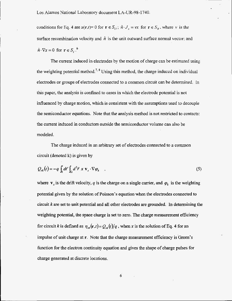
The current induced in electrodes by the motion of charge can be estimated using
the weighting potential method.’. * Using this method, the charge induced on individual
electrodes or groups of eliectrodes connected to a common circuit can be determined. In
this paper, the analysis is confined to cases in which the electrode potential is not
influenced by charge motion, which is consistent with the assumptions used to decouple
the semiconductor equations. Note that the analysis method is not restricted to contacts:
the current induced in conductors outside the semiconductor volume can also be
modeled.
The charge induced in an arbitrary set of electrodes connected to a cornmon
circuit (denoted k) is given by
Qxk(f )=-q l d f ’ s R d3F X V x . v p k .
where v, is the drift velocity, q is the c,,arge on a single carrier, and qk is the weighting
potential given by the soliution of Poisson’s equation when the electrodes connected to
circuit k are set to unit potential and all other electrodes are grounded. In determining the
weighting potential, the space charge is set to zero. The charge measurement efficiency
for circuit k is defined as qxk (r,r) = Qx. (t)/q , when x is the solution of Eq. 4 for an
impulse of unit charge at r. Note that the charge measurement efficiency is Green’s
function for the electron continuity equation and gives the shape of charge pulses for
charge generated at discrete locations.
6

Los Alamos National Laboratory document LA-UR-98- 1 740.
Equations 4 and 5 provide a complete description of charge transport and current
induction for excess carriers produced by radiation interactions. The steady -state electric
field, which appears in the excess carrier continuity equation, can be determined bj.
solving the semiconductor equations (Eqs. 1-3). The boundary conditions for Eq. 4 are
general enough to model a wide variety of semiconductor effects. Equation 5 can be used
to approximate the output of a charge-sensitive preamplifier and is the starting point for
more detailed calculations of the response of pulse-processing electronics. Ballistic
deficit, for example, can be modeled by convolving the charge pulse given by Eq. 5 with
the transfer function of the charge-sensitive preamplifier.
PULSE MAPPING METHOD
An efficient method can be derived for estimating all of the pulses that can be
produced by a detector for a selected circuit and charge carrier. Since the excess carrier
continuity equation involves linear operators, an adjoint continuity equation can be
constructed. For example, the adjoint electron continuity equation is given by
-- an+ - -,U,~V p - Vn' + V e (DnVn+)- n+/z,, + Gl , dt
where n+ is the adjoint electron concentration. If the adjoint generation term is selected
to be G,' = p , l V p - V ~ k , then the solution to Eq. 6 yields a spatial and temporal map of
the charge measurement efficiency for circuit k. Namely, it can be shown that
n+(r,t)= vnk(r,r) . (7)
In other words, all of the charge pulses that can be produced by a detector for impulses of
charge at discrete locations can be determined by solving a single, time-dependent
problem.
7

Los Alamos National Laboratory document LA-UR-98- 1 740.
The boundary conditions for Eq. 6 are given in Table 1. All of the assumptions
that are stated for Eqs. 4 and 5 are valid for the adjoint model. An expression similar to
Eq. 6 can be developed for excess holes with the same interpretation. ni (r.1) = qPk (r-l) .
The generation term for the adjoint hole continuity equation is G; = ,upVp. V v L . and the
sign is reversed on the drift term (see Table 1).
DETRAPPING
Detrapping of carriers causes additional dispersion of charge, delays charge
collection, and enhances ballistic deficit. Detrapping can be included in the model by
introducing an additional continuity equation describing the population of trapped
carriers. For the model to be strictly valid, the number of unoccupied trapping centers
must be large compared tlo the number of excess free carriers. The continuity equation is
given by
an, - = ./TI, - n, at
,
where n, is the concentration of trapped, excess carriers and z,: is the lifetime of trapped
carriers. By definition, there are no excess, trapped carriers in steady state, so
n, (r,O) = 0. The adjoint equation for trapped carriers is
+ I * an+ - = .+/TI, -n, 1 z,, , at
(9)
where the initial condition for the concentration of trapped adjoint carriers is n+(r,O) = 0 .
It is very easy to show that the solution of the coupled system of adjoint equations (Eqs. 6
8

Los Alamos National Laboratory document LA-UR-98- 1 740.
and 9) has the same interpretation as before: n- ( r . t )= v,,~ (r.r). So. a map of charge
pulses can be constructed that includes both trapping and detrapping.
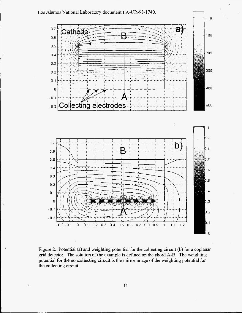
SIMPLE DEMONSTRATION
To illustrate the mapping method. we calculated charge-pulses for points
underneath a collecting electrode in a coplanar grid CdZnTe detector. Luke gives a
detailed description of the coplanar grid method.
cm x 0.5 cm and is described in detail e1~ewhere.l~ The electrostatic potential and the
weighting potential for both the collecting and noncollecting electrodes were determined
using a two-dimensional finite elements code (Fig. 2). Space charge was neglected. The
mobility of electrons was assumed to be 600 cm2N-s. The electron lifetime was 5 ps.
Detrapping was not modeled. The adjoint electron continuity equation (Eq. 6 ) was
solved in 25-ns time steps using finite differences in one dimension along the chord A-B
shown in Fig. 1. Lateral charge motion was ignored. The electrostatic potential and
weighting potential for the collecting and noncollecting circuit used in the calculation are
shown in Fig. 3. The results of the simulation, including Green’s function for charge
induction by electrons, are displayed in Fig. 4. Note that the adjoint electrons flow in the
same direction as the holes. In fact, if there is no space charge in the device, the adjoint
continuity equation has exactly the same form as the continuity equation for holes (see
Table 1 ). Consequently, production semiconductor codes can easily be modified to solve
The device modeled was 1 cm x 1 11.12
the adjoint continuity equation for Green’s function, provided the adjoint source term can
be modeled and the user is willing to ignore the effect of space charge on the adjoint drift
term.
9

~~ ~ ~
Los Alamos National Laboratory document LA-UR-98- 1 740.
CONCLUSIONS
The adjoint mapping method enables the efficient calculation of charge-pulses
produced by semiconductor radiation detectors: the solution of a single, time-dependent
problem is required to compute Green’s function for selected electrodes. provided the
weighting potential for the electrodes and the steady-state electric field within the device
are known. The underlying assumptions of the method are consistent with assumptions
routinely used for semiconductor detector analysis. For example, for planar detectors, the
model is consistent with Hecht’s relation. Within the framework of the mapping
algorithm, a wide range of carrier transport physics can be modeled, including trapping
and detrapping, the diffusion and drift of charge carriers, arbitrary electric fields, and
non-ideal contacts (e.g., Schottky effect). No assumptions are made about the geometry
of the device or the electrodes. Consequently, the mapping method should prove
effective in modeling complex structures envisioned for compound semiconductor
detectors and imagers.
ACKNOWLEDGEMENTS
This work was conducted with funding from Los Alamos Nati(ma1 Laboratory Directed
Research and Development through the Department of Energy under contract W-7405-
ENG-36.
IO
Los Alamos National Laboratory document LA-UR-98- 1 740.
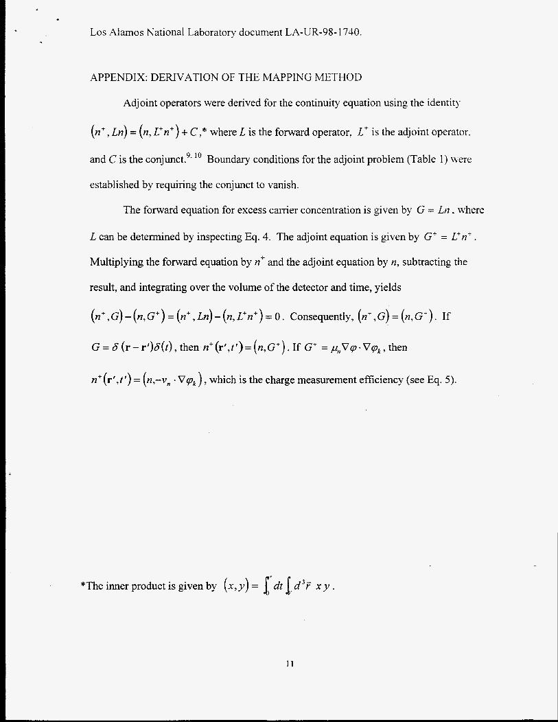
APPENDIX: DERIVATION OF THE MAPPING METHOD
Adjoint operators were derived for the continuity equation using the identity
(n+, Ln) = (n, L+n+) + C,* where L is the forward operator. L’ is the adjoint operator.
and C is the conjunct? l o Boundary conditions for the adjoint problem (Table 1) \\-ere
established by requiring the conjunct to vanish.
The forward equation for excess carrier concentration is given by G = Liz, where
L can be determined by inspecting Eq. 4. The adjoint equation is given by G’ = L+n- .
Multiplying the forward equation by nf and the adjoint equation by n, subtracting the
result, and integrating over the volume of the detector and time, yields
(.+,G)-(~,G+) = ( n + , ~ n ) - ( n , ~ + n + ) = 0 . Consequently, ( n + , ~ ) = (.,G+). If
G=6( r - r ’ )6 ( t ) , then n + ( r ’ , t f ) = ( n , G + ) . If G+ = p , , V q . V q k , then
n+(r’,f‘) = (n,-v,, - V q k ) , which is the charge measurement efficiency (see Eq. 5).
*The inner product is given by (x ,y ) = l d t [,d3F x y .
11

REFERENCES
[ 13 S. Selberherr, Analysis and Simulation of Semiconductor Devices. Springer-Verlap. Vienna, 1984.
[2] R. Trammel1 and F. J. Walter, “The effects of carrier trappins in semiconductor gamma-ray spectrometers,” Nucl. Instrum. Meth. 76, pp. 3 17-32 1 (1 969).
[3] H. H. Barren, J. D. Eskin, and H. B. Barber, “Charge Transport in Arrays of Semiconductor Gamma-Ray Detectors,’. Phys. Rev. Lett. Vol. 75, Num. 1 , pp. 156- 159 (1 995).
[4] Th. Kroll, et al., “Analysis of simulated and measured pulse shapes of closed-ended HPGe detectors,” Nucl. Instrum. Meth. Phys. Res. A 37 1, pp. 489-496 (1 996).
[SI L.-A. Hamel and S. P,aquet, “Charge transport and signal generation in CdTe pixel detectors,”Nucl, instrum. Meth. Phys. Res. A 380, pp. 238-240 (1996).
[6] S. M. Sze, Physics of Semiconductor Devices 2nd Edition, John Wiley & Sons. New York, 198 1.
[7] S. Ramo, “Currents induced by electron motion,” Proc. I.R.E. Vol. 27, pp. 584-585 (September, 1939).
[SI V. Radeka, “Low-noise techniques in detectors,” Ann. Rev. Nucl. Part. Sci. 38. pp.
[9] G. I. Bell and S. Glasstone, Nuclear Reactor Theory, Van Nostrand Reinhold Co., New York, 1970.
[ 1 O]G. Arfken, Mathematical Methods for Physicists, Academic Press, Inc., New York, 1966.
[ 1 1]P. N. Luke (Novembtx 28, 1994) “Single-Polarity Charge Sensing in Ionization Detectors Using Coplanar Electrodes”, Appl. Phys. Lett. Vol. 65, pp. 2884-2887.
[ 12lP. N. Luke, et al., (November, 1996), “Electrode Design for Coplanar-Grid Detectors,” IEEE TRANSACTIONS ON NUCLEAR SCIENCE, Vol. 44(#3/pt. 1) pp.
217-277 (1988).
71 3-720 1997. [13]Prettyman, T. H., et al., “Physics-Based Generation of Gamma-Ray Response
Functions for CdZnTe Detectors,” Journal of Radioanalytical and Nuclear Chemistry Vol. 233, NO. 1-2, to appear (1998).
12

Los Alamos National Laboratory document LA-UR-98- 1 740.
,,Rectifying contacts (e.g., gold or platinum)
c' y-ray Ohmic contact
(e.g., gold-germanium alloy) r E S B
Figure 1. Diagram of a coplanar-grid detector illustrating different types of boundaries.
Table 1. Summary of operators and boundary conditions for the electron continuity equation. Forward Adjoint Associated initial and boundary conditions
- an an+ n+(r,O)= o v r E at at t 2 0 v * ( P , P V d
v * (QV4
Notes: 1. The adjoint model is derived as a final value problem and has been transformed into an
initial value problem by a change of variables. 2. - , ~ , ~ V q e Vn+ = -V - (n+p,,Vq) if V2q = 0 and p,? is spatially invariant, in which case
the adjoint electron continuity equation has the same form as the hole continuity equation.
for the adjoint problem.
- (Note 1 )
n+ (r, t ) = o v r E S, v S, (Note 4)
Ti.Vn+ = O \d r E S, US, n+(r, t )=O v rESo
- p , , ~ - Vn' (Notes 2 and 3)
v - (DJn+)
3. The adjoint term for the hole continuity equation isp,Vq-Vp+. 4. This condition can be eliminated on surfaces for which h e V q = 0 .
13
Los Alamos National Laboratory document LA-UR-98- 1 740.
0 .?
0.6
0.5
0.4
0.3
0.2
0 . I
0
- 0.1
- 0 . 2
I 1 I I I I 1 I I I I I I I I I 1
- 0.2 -0 .1 0 0.1 0 . 2 0.3 0 .4 0.5 0.6 0.7 0.8 0.9 1 1 .1 1.2
100
200
300
1
.9
.8
.
Figure 2. Potential (a) arid weighting potential for the collecting circuit (b) for a coplanar grid detector. The solution of the example is defined on the chord A-B. The weighting potential for the noncollecting circuit is the mirror image of the weighting potential for the collecting circuit.
14

Los Alamos National Laboratory document LA-UR-98- 1 740.
3000
2000
1000
0
-1 000
-2000
;\ i
j -1OOV(Dn I
J
-3000 0 0.1 0.4 0.5
Figure 3. Electric field and weighting fields for the collecting and noncollecting electrodes, where z is the distance fiom the anode.
15

Los Alamos National Laboratory document LA-UR-98-1740.
40
i I
11 1
z (CITI)
0.5
0
-0.5 I
- I b)
OL - i I
-5! I
i -10- / ~
1 -20 I
0 1 0 2 0 3 0 4 0 5 -35;
z (cm) 0.4
I d)
-0.6; I 0.1 0.2 0.3 0.4 0.5
(cm)
0.5 -
0
-0.5
0 0.1 0.2 0.3 0.4 0.5 Time (microseconds)
0 0.1 0.2 0.3 0.4 0.5
Time (microseconds) Figure 4. The adjoint generation terms for the collecting and noncollecting electrodes are shown in 4a and 4b, respectively, where z is the distance from the anode. The adjoint electron concentrations (Green’s function) for the collecting and noncollecting electrodes are shown in 4c and 4d, respectively. Adjoint electrons move towards the cathode (as do holes). Charge pulses determined from the adjoint solutions are shown as a function of depth in 4e and 4f for the collecting and noncollecting electrodes, respectively.
16