Embed Size (px)
Citation preview
TL082-N
www.ti.com SNOSBW5C –APRIL 1998–REVISED APRIL 2013
TL082 Wide Bandwidth Dual JFET Input Operational AmplifierCheck for Samples: TL082-N
1FEATURES DESCRIPTIONThese devices are low cost, high speed, dual JFET
23• Internally Trimmed Offset Voltage: 15 mVinput operational amplifiers with an internally trimmed
• Low Input Bias Current: 50 pA input offset voltage ( BI-FET II™ technology). They• Low Input Noise Voltage: 16nV/√Hz require low supply current yet maintain a large gain
bandwidth product and fast slew rate. In addition, well• Low Input Noise Current: 0.01 pA/√Hzmatched high voltage JFET input devices provide• Wide Gain Bandwidth: 4 MHz very low input bias and offset currents. The TL082 is
• High Slew Rate: 13 V/μs pin compatible with the standard LM1558 allowingdesigners to immediately upgrade the overall• Low Supply Current: 3.6 mAperformance of existing LM1558 and most LM358• High Input Impedance: 1012Ωdesigns.
• Low Total Harmonic Distortion: ≤0.02%These amplifiers may be used in applications such as• Low 1/f Noise Corner: 50 Hz high speed integrators, fast D/A converters, sample
• Fast Settling Time to 0.01%: 2 μs and hold circuits and many other circuits requiring lowinput offset voltage, low input bias current, high inputimpedance, high slew rate and wide bandwidth. Thedevices also exhibit low noise and offset voltage drift.
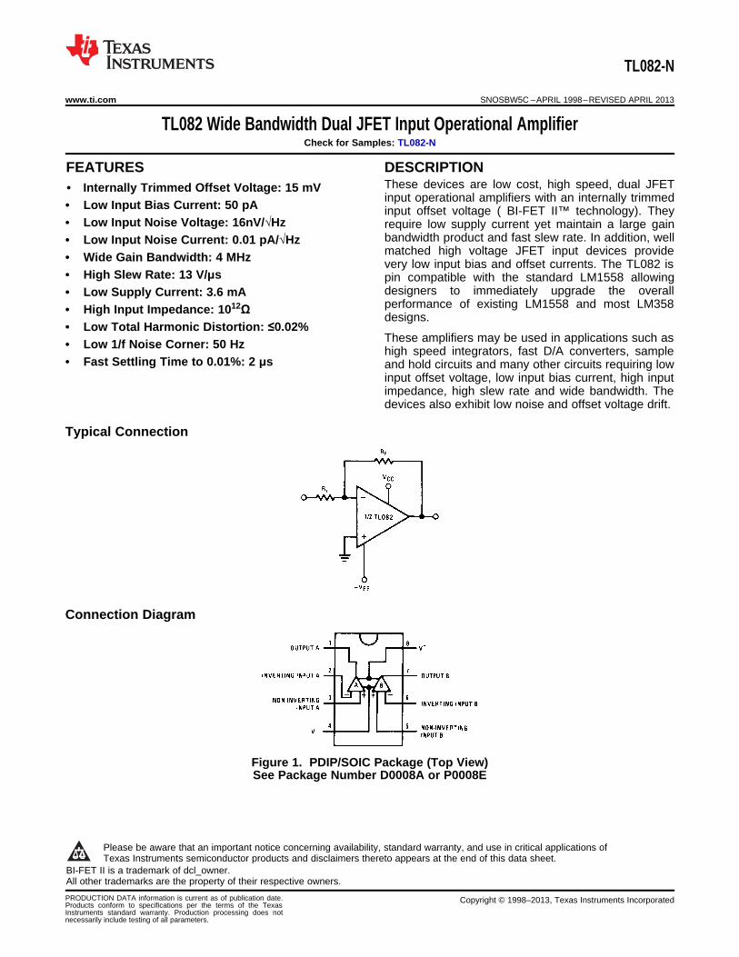
Typical Connection
Connection Diagram
Figure 1. PDIP/SOIC Package (Top View)See Package Number D0008A or P0008E
1
Please be aware that an important notice concerning availability, standard warranty, and use in critical applications ofTexas Instruments semiconductor products and disclaimers thereto appears at the end of this data sheet.
2BI-FET II is a trademark of dcl_owner.3All other trademarks are the property of their respective owners.
PRODUCTION DATA information is current as of publication date. Copyright © 1998–2013, Texas Instruments IncorporatedProducts conform to specifications per the terms of the TexasInstruments standard warranty. Production processing does notnecessarily include testing of all parameters.
TL082-N
SNOSBW5C –APRIL 1998–REVISED APRIL 2013 www.ti.com
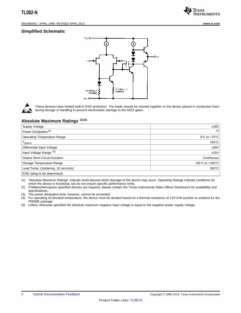
Simplified Schematic
These devices have limited built-in ESD protection. The leads should be shorted together or the device placed in conductive foamduring storage or handling to prevent electrostatic damage to the MOS gates.
Absolute Maximum Ratings (1) (2)
Supply Voltage ±18V
Power Dissipation (3) (4)
Operating Temperature Range 0°C to +70°C
Tj(MAX) 150°C
Differential Input Voltage ±30V
Input Voltage Range (5) ±15V
Output Short Circuit Duration Continuous
Storage Temperature Range −65°C to +150°C
Lead Temp. (Soldering, 10 seconds) 260°C
ESD rating to be determined.
(1) “Absolute Maximum Ratings” indicate limits beyond which damage to the device may occur. Operating Ratings indicate conditions forwhich the device is functional, but do not ensure specific performance limits.
(2) If Military/Aerospace specified devices are required, please contact the Texas Instruments Sales Office/ Distributors for availability andspecifications.
(3) The power dissipation limit, however, cannot be exceeded.(4) For operating at elevated temperature, the device must be derated based on a thermal resistance of 115°C/W junction to ambient for the
P0008E package.(5) Unless otherwise specified the absolute maximum negative input voltage is equal to the negative power supply voltage.
2 Submit Documentation Feedback Copyright © 1998–2013, Texas Instruments Incorporated
Product Folder Links: TL082-N
TL082-N
www.ti.com SNOSBW5C –APRIL 1998–REVISED APRIL 2013
DC Electrical Characteristics (1)
TL082CSymbol Parameter Conditions Units
Min Typ Max
VOS Input Offset Voltage RS = 10 kΩ, TA = 25°C 5 15 mV
Over Temperature 20 mV
ΔVOS/ΔT Average TC of Input Offset Voltage RS = 10 kΩ 10 μV/°C
IOS Input Offset Current Tj = 25°C, (1) (2) 25 200 pA
Tj ≤ 70°C 4 nA
IB Input Bias Current Tj = 25°C, (1) (2) 50 400 pA
Tj ≤ 70°C 8 nA
RIN Input Resistance Tj = 25°C 1012 ΩAVOL Large Signal Voltage Gain VS = ±15V, TA = 25°C, 25 100 V/mV
VO = ±10V, RL = 2 kΩOver Temperature 15 V/mV
VO Output Voltage Swing VS = ±15V, RL = 10 kΩ ±12 ±13.5 V
VCM Input Common-Mode Voltage VS = ±15V ±11 +15 VRange −12 V
CMRR Common-Mode Rejection Ratio RS ≤ 10 kΩ 70 100 dB
PSRR Supply Voltage Rejection Ratio (3) 70 100 dB
IS Supply Current 3.6 5.6 mA
(1) These specifications apply for VS = ±15V and 0°C ≤TA ≤ +70°C. VOS, IB and IOS are measured at VCM = 0.(2) The input bias currents are junction leakage currents which approximately double for every 10°C increase in the junction temperature,
Tj. Due to the limited production test time, the input bias currents measured are correlated to junction temperature. In normal operationthe junction temperature rises above the ambient temperature as a result of internal power dissipation, PD. Tj = TA + θjA PD where θjA isthe thermal resistance from junction to ambient. Use of a heat sink is recommended if input bias current is to be kept to a minimum.
(3) Supply voltage rejection ratio is measured for both supply magnitudes increasing or decreasing simultaneously in accordance withcommon practice. VS = ±6V to ±15V.
AC Electrical Characteristics (1)
TL082CSymbol Parameter Conditions Units
Min Typ Max
Amplifier to Amplifier Coupling TA = 25°C, f = 1Hz-20 kHz −120 dB(Input Referred)
SR Slew Rate VS = ±15V, TA = 25°C 8 13 V/μs
GBW Gain Bandwidth Product VS = ±15V, TA = 25°C 4 MHz
en Equivalent Input Noise Voltage TA = 25°C, RS = 100Ω, 25 nV/√Hzf = 1000 Hz
in Equivalent Input Noise Current Tj = 25°C, f = 1000 Hz 0.01 pA/√Hz
THD Total Harmonic Distortion AV = +10, RL = 10k, <0.02 %VO = 20 Vp − p,BW = 20 Hz−20 kHz
(1) These specifications apply for VS = ±15V and 0°C ≤TA ≤ +70°C. VOS, IB and IOS are measured at VCM = 0.
Copyright © 1998–2013, Texas Instruments Incorporated Submit Documentation Feedback 3
Product Folder Links: TL082-N
TL082-N
SNOSBW5C –APRIL 1998–REVISED APRIL 2013 www.ti.com
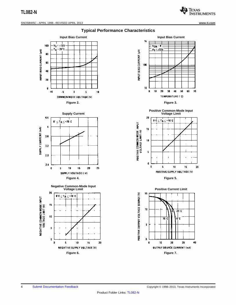
Typical Performance Characteristics
Input Bias Current Input Bias Current
Figure 2. Figure 3.
Positive Common-Mode InputSupply Current Voltage Limit
Figure 4. Figure 5.
Negative Common-Mode InputVoltage Limit Positive Current Limit
Figure 6. Figure 7.
4 Submit Documentation Feedback Copyright © 1998–2013, Texas Instruments Incorporated
Product Folder Links: TL082-N
TL082-N
www.ti.com SNOSBW5C –APRIL 1998–REVISED APRIL 2013
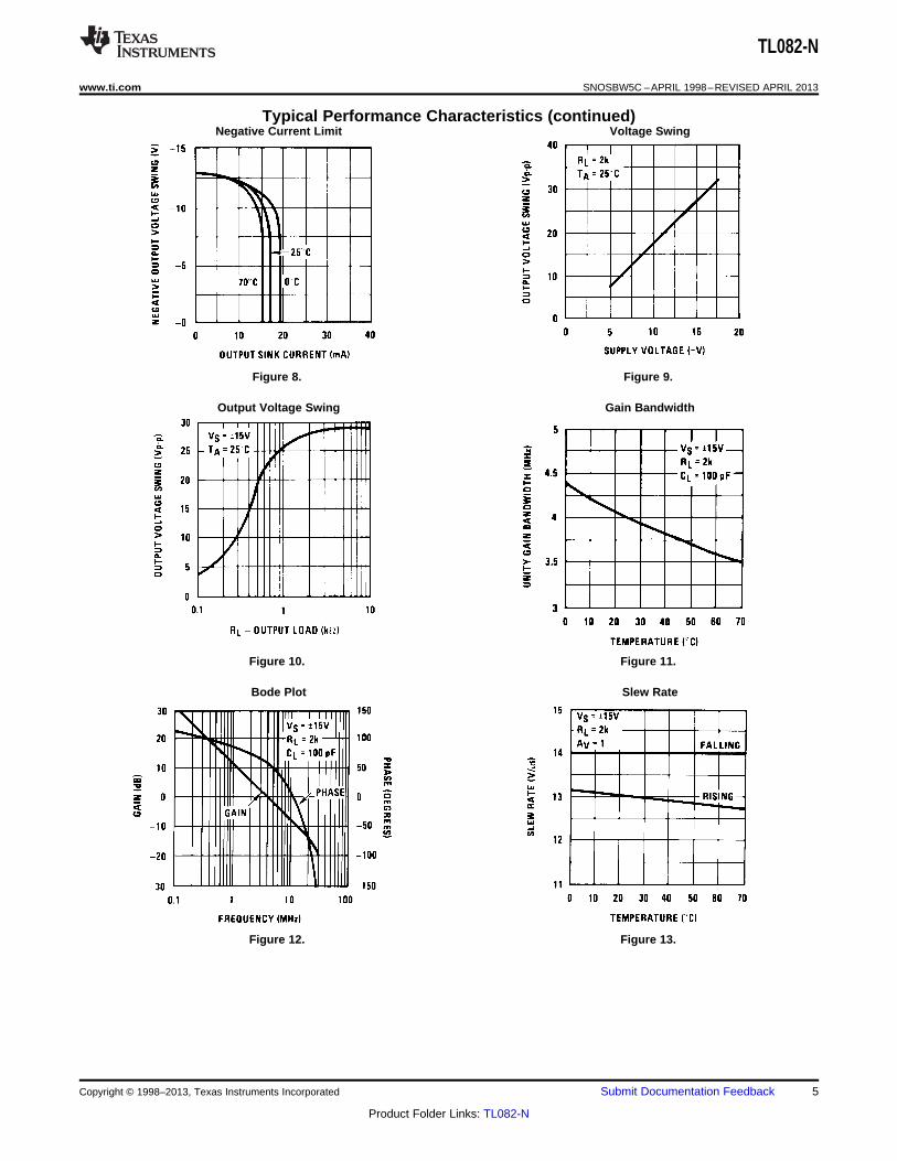
Typical Performance Characteristics (continued)Negative Current Limit Voltage Swing
Figure 8. Figure 9.
Output Voltage Swing Gain Bandwidth
Figure 10. Figure 11.
Bode Plot Slew Rate
Figure 12. Figure 13.
Copyright © 1998–2013, Texas Instruments Incorporated Submit Documentation Feedback 5
Product Folder Links: TL082-N
TL082-N
SNOSBW5C –APRIL 1998–REVISED APRIL 2013 www.ti.com
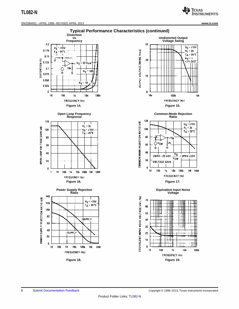
Typical Performance Characteristics (continued)Distortion
vs Undistorted OutputFrequency Voltage Swing
Figure 14. Figure 15.
Open Loop Frequency Common-Mode RejectionResponse Ratio
Figure 16. Figure 17.
Power Supply Rejection Equivalent Input NoiseRatio Voltage
Figure 18. Figure 19.
6 Submit Documentation Feedback Copyright © 1998–2013, Texas Instruments Incorporated
Product Folder Links: TL082-N
TL082-N
www.ti.com SNOSBW5C –APRIL 1998–REVISED APRIL 2013
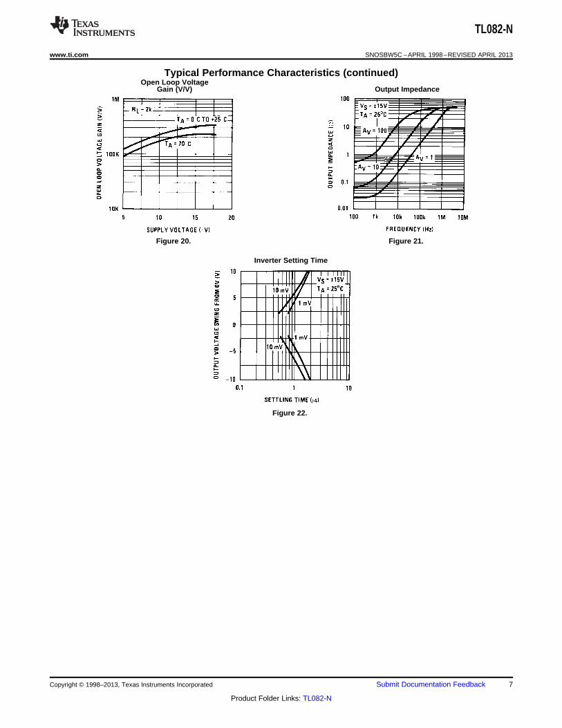
Typical Performance Characteristics (continued)Open Loop Voltage
Gain (V/V) Output Impedance
Figure 20. Figure 21.
Inverter Setting Time
Figure 22.
Copyright © 1998–2013, Texas Instruments Incorporated Submit Documentation Feedback 7
Product Folder Links: TL082-N
TL082-N
SNOSBW5C –APRIL 1998–REVISED APRIL 2013 www.ti.com
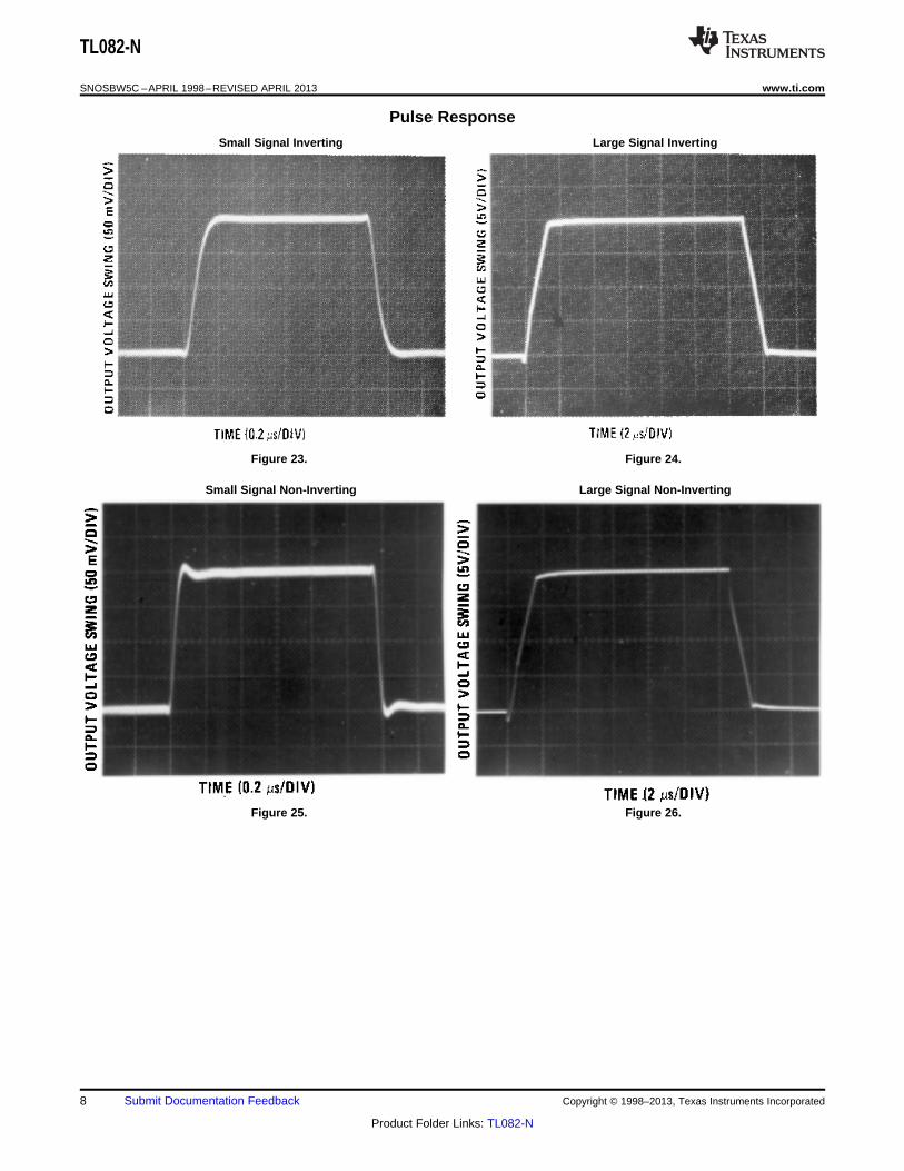
Pulse Response
Small Signal Inverting Large Signal Inverting
Figure 23. Figure 24.
Small Signal Non-Inverting Large Signal Non-Inverting
Figure 25. Figure 26.
8 Submit Documentation Feedback Copyright © 1998–2013, Texas Instruments Incorporated
Product Folder Links: TL082-N
TL082-N
www.ti.com SNOSBW5C –APRIL 1998–REVISED APRIL 2013
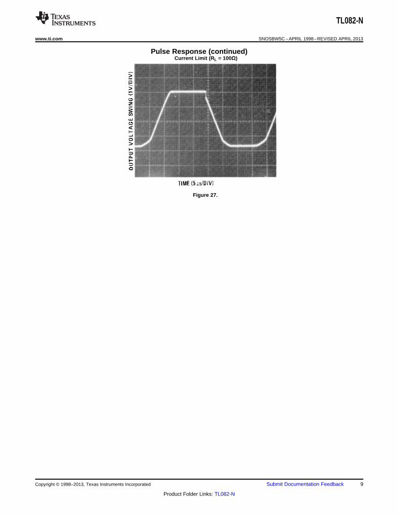
Pulse Response (continued)Current Limit (RL = 100Ω)
Figure 27.
Copyright © 1998–2013, Texas Instruments Incorporated Submit Documentation Feedback 9
Product Folder Links: TL082-N
TL082-N
SNOSBW5C –APRIL 1998–REVISED APRIL 2013 www.ti.com
APPLICATION HINTS
These devices are op amps with an internally trimmed input offset voltage and JFET input devices (BI-FET II).These JFETs have large reverse breakdown voltages from gate to source and drain eliminating the need forclamps across the inputs. Therefore, large differential input voltages can easily be accommodated without a largeincrease in input current. The maximum differential input voltage is independent of the supply voltages. However,neither of the input voltages should be allowed to exceed the negative supply as this will cause large currents toflow which can result in a destroyed unit.
Exceeding the negative common-mode limit on either input will cause a reversal of the phase to the output andforce the amplifier output to the corresponding high or low state. Exceeding the negative common-mode limit onboth inputs will force the amplifier output to a high state. In neither case does a latch occur since raising the inputback within the common-mode range again puts the input stage and thus the amplifier in a normal operatingmode.
Exceeding the positive common-mode limit on a single input will not change the phase of the output; however, ifboth inputs exceed the limit, the output of the amplifier will be forced to a high state.
The amplifiers will operate with a common-mode input voltage equal to the positive supply; however, the gainbandwidth and slew rate may be decreased in this condition. When the negative common-mode voltage swingsto within 3V of the negative supply, an increase in input offset voltage may occur.
Each amplifier is individually biased by a zener reference which allows normal circuit operation on ±6V powersupplies. Supply voltages less than these may result in lower gain bandwidth and slew rate.
The amplifiers will drive a 2 kΩ load resistance to ±10V over the full temperature range of 0°C to +70°C. If theamplifier is forced to drive heavier load currents, however, an increase in input offset voltage may occur on thenegative voltage swing and finally reach an active current limit on both positive and negative swings.
Precautions should be taken to ensure that the power supply for the integrated circuit never becomes reversed inpolarity or that the unit is not inadvertently installed backwards in a socket as an unlimited current surge throughthe resulting forward diode within the IC could cause fusing of the internal conductors and result in a destroyedunit.
Because these amplifiers are JFET rather than MOSFET input op amps they do not require special handling.
As with most amplifiers, care should be taken with lead dress, component placement and supply decoupling inorder to ensure stability. For example, resistors from the output to an input should be placed with the body closeto the input to minimize “pick-up” and maximize the frequency of the feedback pole by minimizing thecapacitance from the input to ground.
A feedback pole is created when the feedback around any amplifier is resistive. The parallel resistance andcapacitance from the input of the device (usually the inverting input) to AC ground set the frequency of the pole.In many instances the frequency of this pole is much greater than the expected 3 dB frequency of the closedloop gain and consequently there is negligible effect on stability margin. However, if the feedback pole is lessthan approximately 6 times the expected 3 dB frequency a lead capacitor should be placed from the output to theinput of the op amp. The value of the added capacitor should be such that the RC time constant of this capacitorand the resistance it parallels is greater than or equal to the original feedback pole time constant.
10 Submit Documentation Feedback Copyright © 1998–2013, Texas Instruments Incorporated
Product Folder Links: TL082-N
TL082-N
www.ti.com SNOSBW5C –APRIL 1998–REVISED APRIL 2013
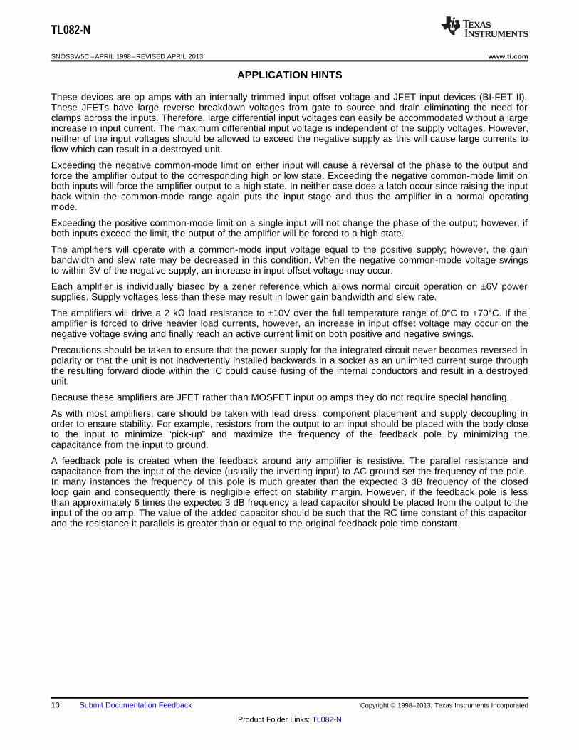
Detailed Schematic
Copyright © 1998–2013, Texas Instruments Incorporated Submit Documentation Feedback 11
Product Folder Links: TL082-N
TL082-N
SNOSBW5C –APRIL 1998–REVISED APRIL 2013 www.ti.com
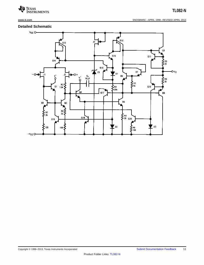
Typical Applications
• All potentiometers are linear taper
• Use the LF347 Quad for stereo applications
All controls flat.
Bass and treble boost, mid flat.
Bass and treble cut, mid flat.
Mid boost, bass and treble flat.
Mid cut, bass and treble flat.
Figure 28. Three-Band Active Tone Control
12 Submit Documentation Feedback Copyright © 1998–2013, Texas Instruments Incorporated
Product Folder Links: TL082-N
TL082-N
www.ti.com SNOSBW5C –APRIL 1998–REVISED APRIL 2013
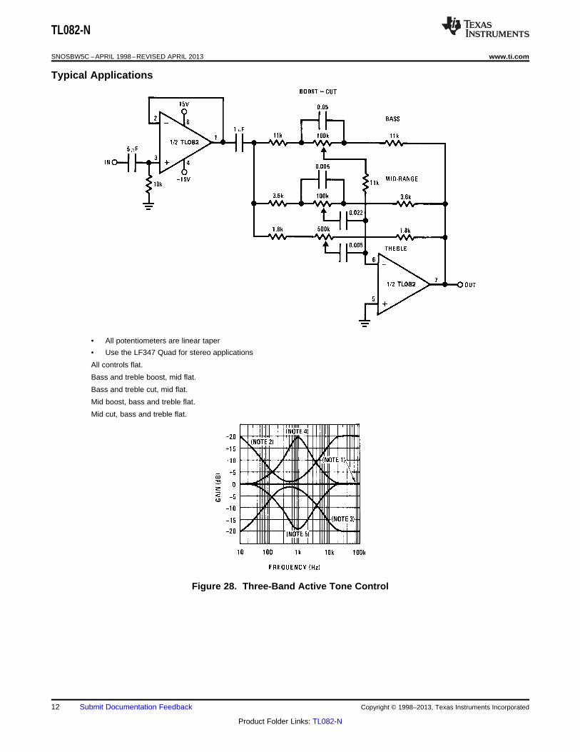
and are separate isolated groundsMatching of R2's, R4's and R5's control CMRRWith AVT = 1400, resistor matching = 0.01%: CMRR = 136 dB
• Very high input impedance
• Super high CMRR
Figure 29. Improved CMRR Instrumentation Amplifier
Copyright © 1998–2013, Texas Instruments Incorporated Submit Documentation Feedback 13
Product Folder Links: TL082-N
TL082-N
SNOSBW5C –APRIL 1998–REVISED APRIL 2013 www.ti.com
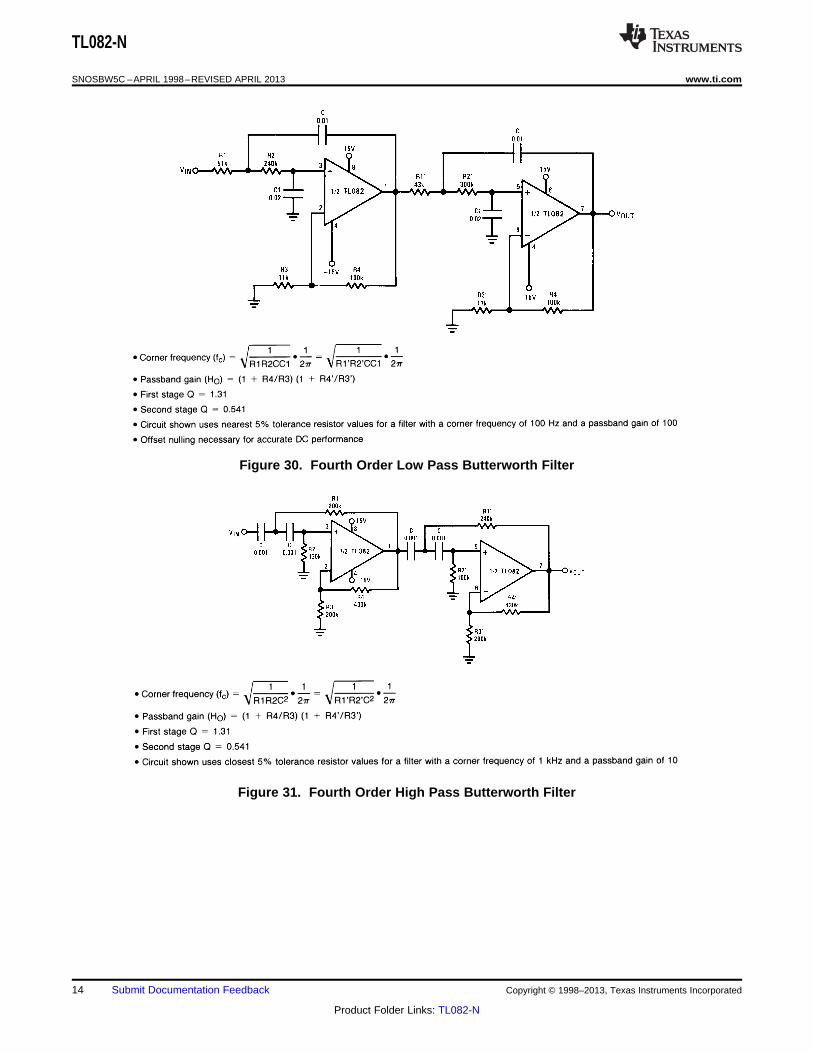
Figure 30. Fourth Order Low Pass Butterworth Filter
Figure 31. Fourth Order High Pass Butterworth Filter
14 Submit Documentation Feedback Copyright © 1998–2013, Texas Instruments Incorporated
Product Folder Links: TL082-N
TL082-N
www.ti.com SNOSBW5C –APRIL 1998–REVISED APRIL 2013
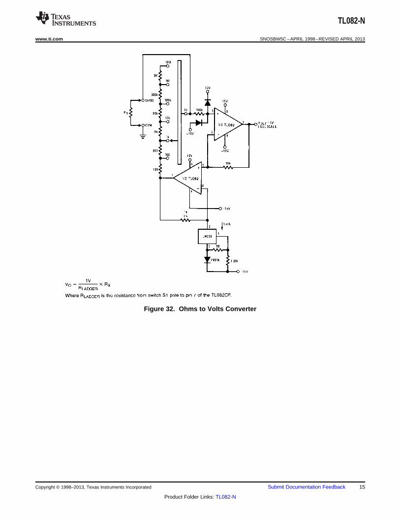
Figure 32. Ohms to Volts Converter
Copyright © 1998–2013, Texas Instruments Incorporated Submit Documentation Feedback 15
Product Folder Links: TL082-N
TL082-N
SNOSBW5C –APRIL 1998–REVISED APRIL 2013 www.ti.com
REVISION HISTORY
Changes from Revision B (April 2013) to Revision C Page
• Changed layout of National Data Sheet to TI format .......................................................................................................... 15
16 Submit Documentation Feedback Copyright © 1998–2013, Texas Instruments Incorporated
Product Folder Links: TL082-N
PACKAGE OPTION ADDENDUM
www.ti.com 10-Dec-2020
Addendum-Page 1
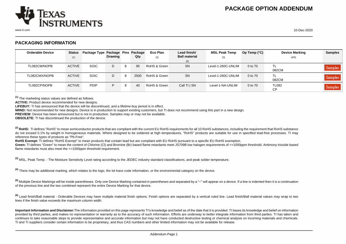
PACKAGING INFORMATION
Orderable Device Status(1)
Package Type PackageDrawing
Pins PackageQty
Eco Plan(2)
Lead finish/Ball material
(6)
MSL Peak Temp(3)
Op Temp (°C) Device Marking(4/5)
Samples
TL082CM/NOPB ACTIVE SOIC D 8 95 RoHS & Green SN Level-1-260C-UNLIM 0 to 70 TL082CM
TL082CMX/NOPB ACTIVE SOIC D 8 2500 RoHS & Green SN Level-1-260C-UNLIM 0 to 70 TL082CM
TL082CP/NOPB ACTIVE PDIP P 8 40 RoHS & Green Call TI | SN Level-1-NA-UNLIM 0 to 70 TL082CP
(1) The marketing status values are defined as follows:ACTIVE: Product device recommended for new designs.LIFEBUY: TI has announced that the device will be discontinued, and a lifetime-buy period is in effect.NRND: Not recommended for new designs. Device is in production to support existing customers, but TI does not recommend using this part in a new design.PREVIEW: Device has been announced but is not in production. Samples may or may not be available.OBSOLETE: TI has discontinued the production of the device.
(2) RoHS: TI defines "RoHS" to mean semiconductor products that are compliant with the current EU RoHS requirements for all 10 RoHS substances, including the requirement that RoHS substancedo not exceed 0.1% by weight in homogeneous materials. Where designed to be soldered at high temperatures, "RoHS" products are suitable for use in specified lead-free processes. TI mayreference these types of products as "Pb-Free".RoHS Exempt: TI defines "RoHS Exempt" to mean products that contain lead but are compliant with EU RoHS pursuant to a specific EU RoHS exemption.Green: TI defines "Green" to mean the content of Chlorine (Cl) and Bromine (Br) based flame retardants meet JS709B low halogen requirements of <=1000ppm threshold. Antimony trioxide basedflame retardants must also meet the <=1000ppm threshold requirement.
(3) MSL, Peak Temp. - The Moisture Sensitivity Level rating according to the JEDEC industry standard classifications, and peak solder temperature.
(4) There may be additional marking, which relates to the logo, the lot trace code information, or the environmental category on the device.
(5) Multiple Device Markings will be inside parentheses. Only one Device Marking contained in parentheses and separated by a "~" will appear on a device. If a line is indented then it is a continuationof the previous line and the two combined represent the entire Device Marking for that device.
(6) Lead finish/Ball material - Orderable Devices may have multiple material finish options. Finish options are separated by a vertical ruled line. Lead finish/Ball material values may wrap to twolines if the finish value exceeds the maximum column width.
Important Information and Disclaimer:The information provided on this page represents TI's knowledge and belief as of the date that it is provided. TI bases its knowledge and belief on informationprovided by third parties, and makes no representation or warranty as to the accuracy of such information. Efforts are underway to better integrate information from third parties. TI has taken andcontinues to take reasonable steps to provide representative and accurate information but may not have conducted destructive testing or chemical analysis on incoming materials and chemicals.TI and TI suppliers consider certain information to be proprietary, and thus CAS numbers and other limited information may not be available for release.
PACKAGE OPTION ADDENDUM
www.ti.com 10-Dec-2020
Addendum-Page 2
In no event shall TI's liability arising out of such information exceed the total purchase price of the TI part(s) at issue in this document sold by TI to Customer on an annual basis.
OTHER QUALIFIED VERSIONS OF TL082-N :
• Automotive: TL082-Q1
NOTE: Qualified Version Definitions:
• Automotive - Q100 devices qualified for high-reliability automotive applications targeting zero defects
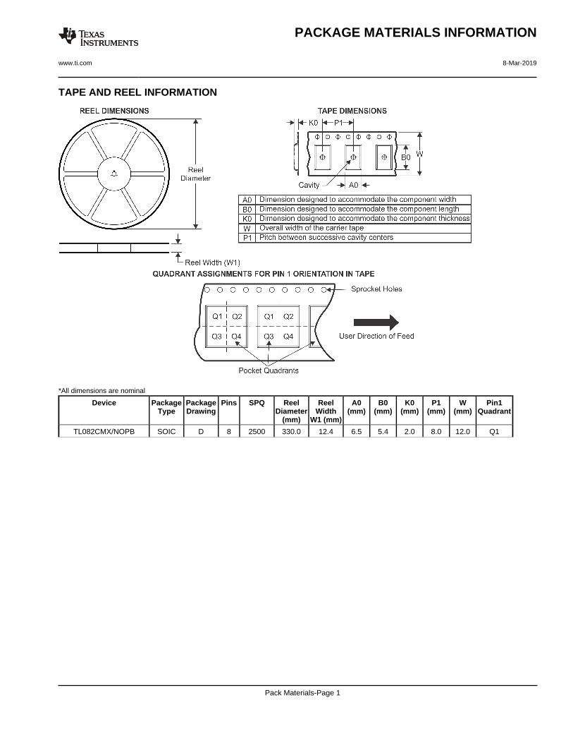
TAPE AND REEL INFORMATION
*All dimensions are nominal
Device PackageType
PackageDrawing
Pins SPQ ReelDiameter
(mm)
ReelWidth
W1 (mm)
A0(mm)
B0(mm)
K0(mm)
P1(mm)
W(mm)
Pin1Quadrant
TL082CMX/NOPB SOIC D 8 2500 330.0 12.4 6.5 5.4 2.0 8.0 12.0 Q1
PACKAGE MATERIALS INFORMATION
www.ti.com 8-Mar-2019
Pack Materials-Page 1
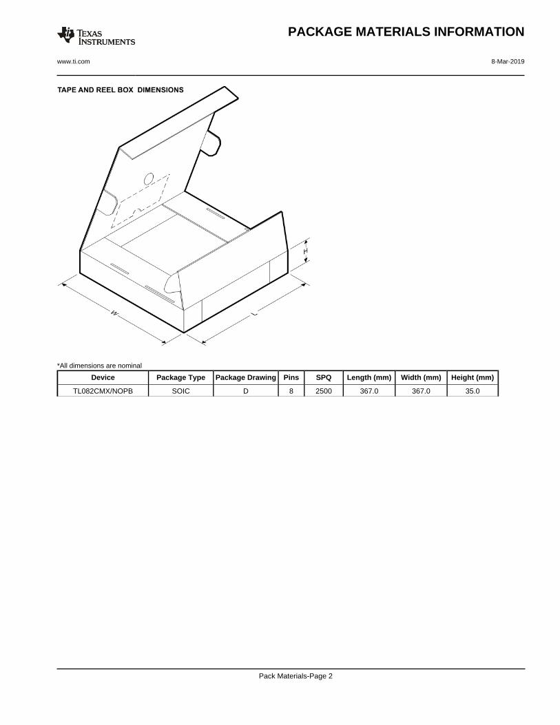
*All dimensions are nominal
Device Package Type Package Drawing Pins SPQ Length (mm) Width (mm) Height (mm)
TL082CMX/NOPB SOIC D 8 2500 367.0 367.0 35.0
PACKAGE MATERIALS INFORMATION
www.ti.com 8-Mar-2019
Pack Materials-Page 2
www.ti.com
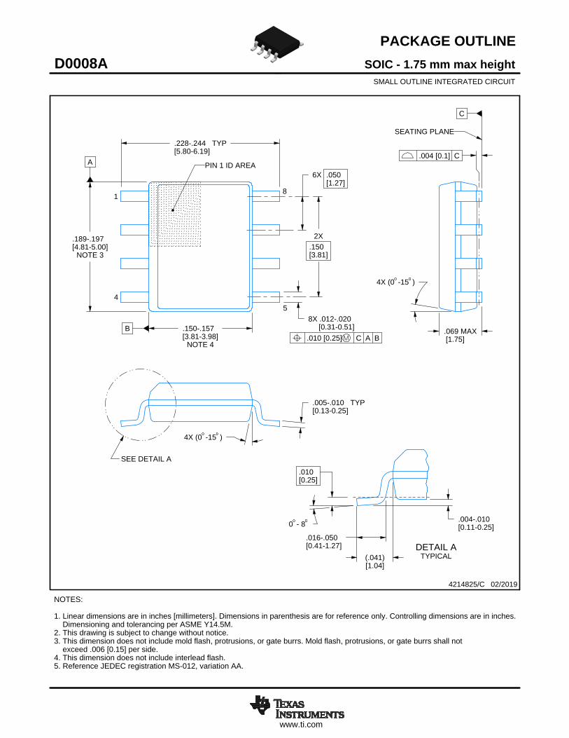
PACKAGE OUTLINE
C
.228-.244 TYP[5.80-6.19]
.069 MAX[1.75]
6X .050[1.27]
8X .012-.020 [0.31-0.51]
2X.150[3.81]
.005-.010 TYP[0.13-0.25]
0 - 8 .004-.010[0.11-0.25]
.010[0.25]
.016-.050[0.41-1.27]
4X (0 -15 )
A
.189-.197[4.81-5.00]
NOTE 3
B .150-.157[3.81-3.98]
NOTE 4
4X (0 -15 )
(.041)[1.04]
SOIC - 1.75 mm max heightD0008ASMALL OUTLINE INTEGRATED CIRCUIT
4214825/C 02/2019
NOTES: 1. Linear dimensions are in inches [millimeters]. Dimensions in parenthesis are for reference only. Controlling dimensions are in inches. Dimensioning and tolerancing per ASME Y14.5M. 2. This drawing is subject to change without notice. 3. This dimension does not include mold flash, protrusions, or gate burrs. Mold flash, protrusions, or gate burrs shall not exceed .006 [0.15] per side. 4. This dimension does not include interlead flash.5. Reference JEDEC registration MS-012, variation AA.
18
.010 [0.25] C A B
54
PIN 1 ID AREA
SEATING PLANE
.004 [0.1] C
SEE DETAIL A
DETAIL ATYPICAL
SCALE 2.800
www.ti.com
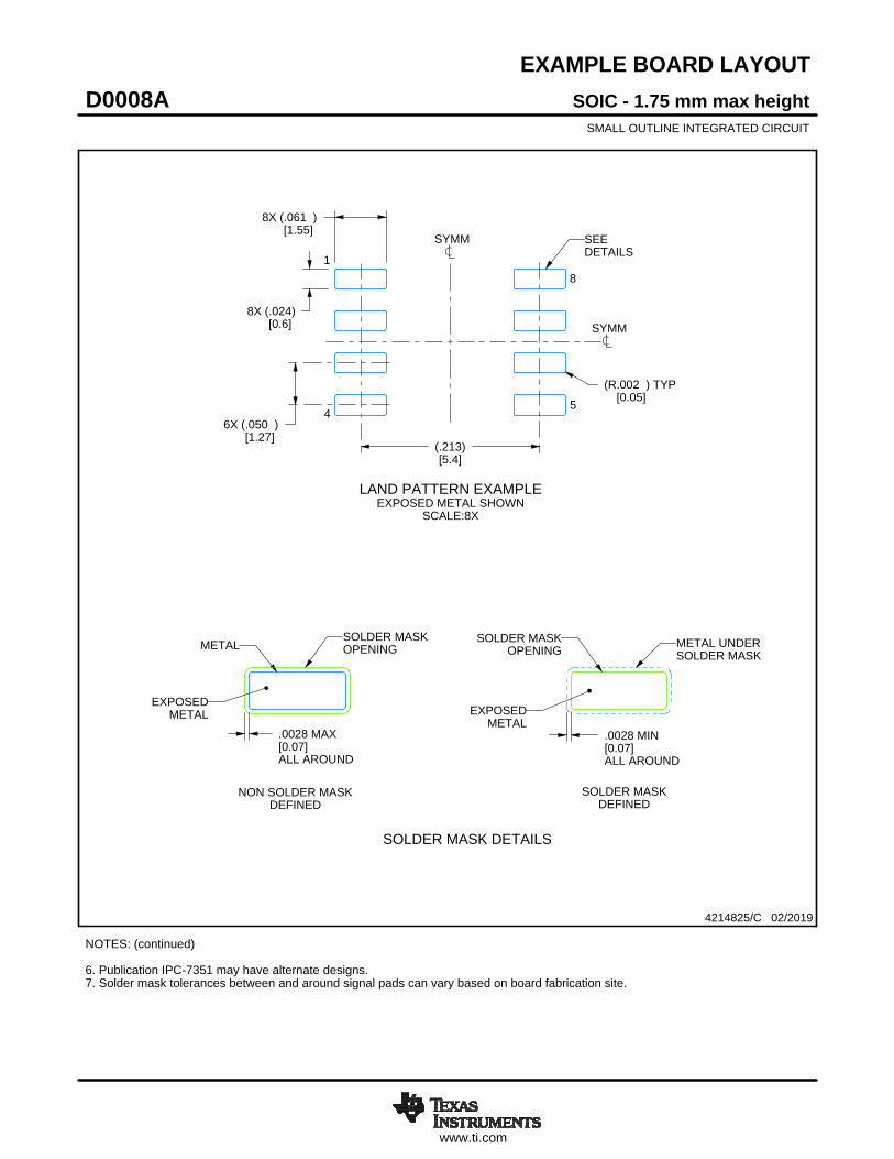
EXAMPLE BOARD LAYOUT
.0028 MAX[0.07]ALL AROUND
.0028 MIN[0.07]ALL AROUND
(.213)[5.4]
6X (.050 )[1.27]
8X (.061 )[1.55]
8X (.024)[0.6]
(R.002 ) TYP[0.05]
SOIC - 1.75 mm max heightD0008ASMALL OUTLINE INTEGRATED CIRCUIT
4214825/C 02/2019
NOTES: (continued) 6. Publication IPC-7351 may have alternate designs. 7. Solder mask tolerances between and around signal pads can vary based on board fabrication site.
METALSOLDER MASKOPENING
NON SOLDER MASKDEFINED
SOLDER MASK DETAILS
EXPOSEDMETAL
OPENINGSOLDER MASK METAL UNDER
SOLDER MASK
SOLDER MASKDEFINED
EXPOSEDMETAL
LAND PATTERN EXAMPLEEXPOSED METAL SHOWN
SCALE:8X
SYMM
1
45
8
SEEDETAILS
SYMM
www.ti.com
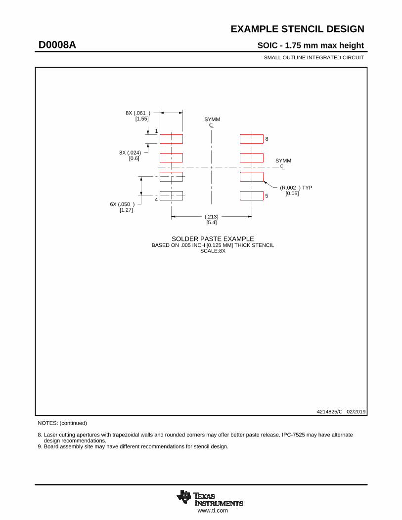
EXAMPLE STENCIL DESIGN
8X (.061 )[1.55]
8X (.024)[0.6]
6X (.050 )[1.27]
(.213)[5.4]
(R.002 ) TYP[0.05]
SOIC - 1.75 mm max heightD0008ASMALL OUTLINE INTEGRATED CIRCUIT
4214825/C 02/2019
NOTES: (continued) 8. Laser cutting apertures with trapezoidal walls and rounded corners may offer better paste release. IPC-7525 may have alternate design recommendations. 9. Board assembly site may have different recommendations for stencil design.
SOLDER PASTE EXAMPLEBASED ON .005 INCH [0.125 MM] THICK STENCIL
SCALE:8X
SYMM
SYMM
1
45
8
IMPORTANT NOTICE AND DISCLAIMER
TI PROVIDES TECHNICAL AND RELIABILITY DATA (INCLUDING DATASHEETS), DESIGN RESOURCES (INCLUDING REFERENCE DESIGNS), APPLICATION OR OTHER DESIGN ADVICE, WEB TOOLS, SAFETY INFORMATION, AND OTHER RESOURCES “AS IS” AND WITH ALL FAULTS, AND DISCLAIMS ALL WARRANTIES, EXPRESS AND IMPLIED, INCLUDING WITHOUT LIMITATION ANY IMPLIED WARRANTIES OF MERCHANTABILITY, FITNESS FOR A PARTICULAR PURPOSE OR NON-INFRINGEMENT OF THIRD PARTY INTELLECTUAL PROPERTY RIGHTS.These resources are intended for skilled developers designing with TI products. You are solely responsible for (1) selecting the appropriate TI products for your application, (2) designing, validating and testing your application, and (3) ensuring your application meets applicable standards, and any other safety, security, or other requirements. These resources are subject to change without notice. TI grants you permission to use these resources only for development of an application that uses the TI products described in the resource. Other reproduction and display of these resources is prohibited. No license is granted to any other TI intellectual property right or to any third party intellectual property right. TI disclaims responsibility for, and you will fully indemnify TI and its representatives against, any claims, damages, costs, losses, and liabilities arising out of your use of these resources.TI’s products are provided subject to TI’s Terms of Sale (www.ti.com/legal/termsofsale.html) or other applicable terms available either on ti.com or provided in conjunction with such TI products. TI’s provision of these resources does not expand or otherwise alter TI’s applicable warranties or warranty disclaimers for TI products.
Mailing Address: Texas Instruments, Post Office Box 655303, Dallas, Texas 75265Copyright © 2020, Texas Instruments Incorporated