Embed Size (px)
Citation preview

TL3472HIGH-SLEW-RATE, SINGLE-SUPPLY OPERATIONAL AMPLIFIER
SLOS200G − OCTOBER 1997 − REVISED JULY 2003
1POST OFFICE BOX 655303 • DALLAS, TEXAS 75265
� Wide Gain-Bandwidth Product . . . 4 MHz
� High Slew Rate . . . 13 V/μs
� Fast Settling Time . . . 1.1 μs to 0.1%
� Wide-Range Single-SupplyOperation . . . 4 V to 36 V
� Wide Input Common-Mode Range IncludesGround (VCC−)
� Low Total Harmonic Distortion . . . 0.02%
� Large-Capacitance DriveCapability . . . 10,000 pF
� Output Short-Circuit Protection
description/ordering information
Quality, low-cost, bipolar fabrication with innovative design concepts is employed for the TL3472 operationalamplifier. This device offers 4 MHz of gain-bandwidth product, 13-V/μs slew rate, and fast settling time, withoutthe use of JFET device technology. Although the TL3472 can be operated from split supplies, it is particularlysuited for single-supply operation because the common-mode input voltage range includes ground potential(VCC−). With a Darlington transistor input stage, this device exhibits high input resistance, low input offsetvoltage, and high gain. The all-npn output stage, characterized by no dead-band crossover distortion and largeoutput voltage swing, provides high-capacitance drive capability, excellent phase and gain margins, lowopen-loop high-frequency output impedance, and symmetrical source/sink ac frequency response. Thislow-cost amplifier is an alternative to the MC33072 and the MC34072 operational amplifiers.
ORDERING INFORMATION
TA PACKAGE† ORDERABLEPART NUMBER
TOP-SIDEMARKING
PDIP (P) Tube of 25 TL3472CP TL3472CP
0°C to 70°CSOIC (D)
Tube of 50 TL3472CD3472C
0 C to 70 CSOIC (D)
Reel of 2500 TL3472CDR3472C
PDIP (P) Tube of 25 TL3472IP TL3472IP
−40°C to 105°CSOIC (D)
Tube of 50 TL3472IDZ3472
40 C to 105 CSOIC (D)
Reel of 2500 TL3472IDRZ3472
† Package drawings, standard packing quantities, thermal data, symbolization, and PCB designguidelines are available at www.ti.com/sc/package.
PRODUCTION DATA information is current as of publication date.Products conform to specifications per the terms of Texas Instrumentsstandard warranty. Production processing does not necessarily includetesting of all parameters.
Copyright © 2003, Texas Instruments Incorporated
Please be aware that an important notice concerning availability, standard warranty, and use in critical applications ofTexas Instruments semiconductor products and disclaimers thereto appears at the end of this data sheet.
1
2
3
4
8
7
6
5
1OUT1IN−1IN+
VCC−/GND
VCC+
2OUT2IN−2IN+
D OR P PACKAGE(TOP VIEW)
TL3472HIGH-SLEW-RATE, SINGLE-SUPPLY OPERATIONAL AMPLIFIER
SLOS200G − OCTOBER 1997 − REVISED JULY 2003
2 POST OFFICE BOX 655303 • DALLAS, TEXAS 75265
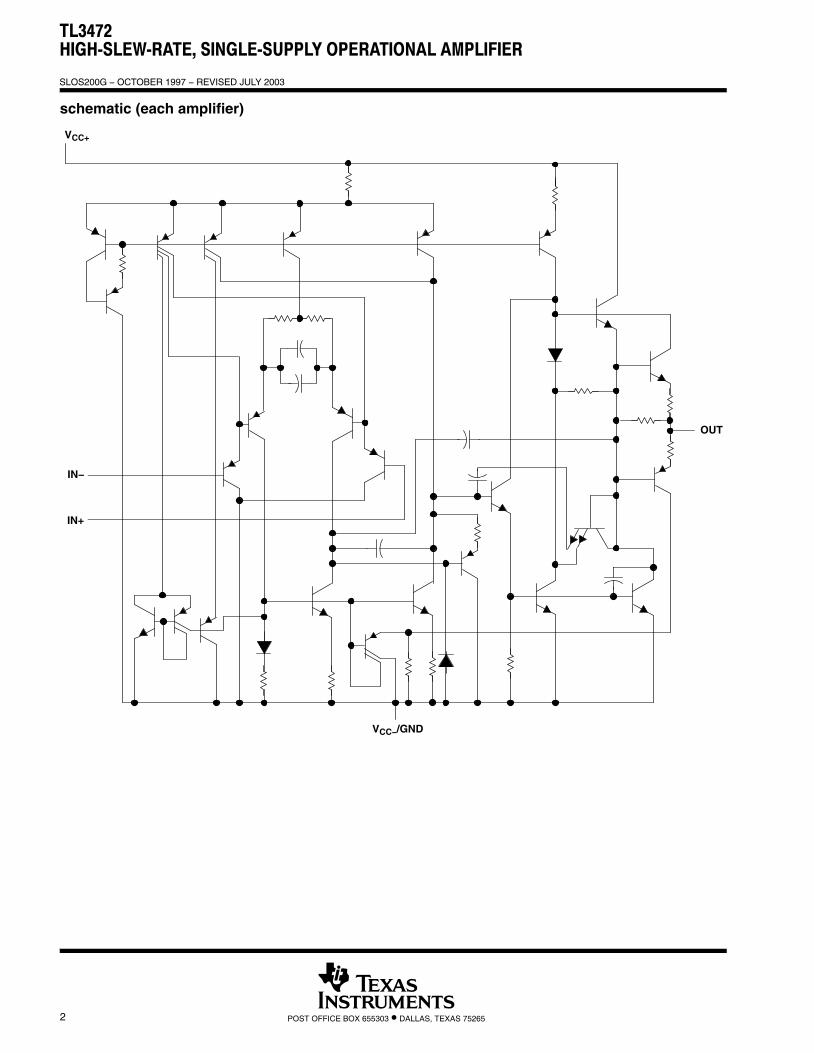
schematic (each amplifier)
VCC+
OUT
VCC−/GND
IN−
IN+
TL3472HIGH-SLEW-RATE, SINGLE-SUPPLY OPERATIONAL AMPLIFIER
SLOS200G − OCTOBER 1997 − REVISED JULY 2003
3POST OFFICE BOX 655303 • DALLAS, TEXAS 75265
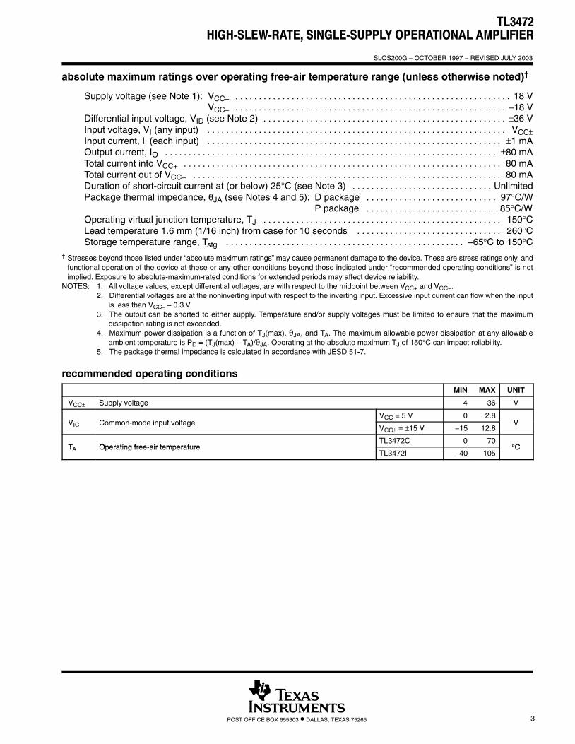
absolute maximum ratings over operating free-air temperature range (unless otherwise noted)†
Supply voltage (see Note 1): VCC+ 18 V. . . . . . . . . . . . . . . . . . . . . . . . . . . . . . . . . . . . . . . . . . . . . . . . . . . . . . . . . . . VCC− −18 V. . . . . . . . . . . . . . . . . . . . . . . . . . . . . . . . . . . . . . . . . . . . . . . . . . . . . . . . . .
Differential input voltage, VID (see Note 2) ±36 V. . . . . . . . . . . . . . . . . . . . . . . . . . . . . . . . . . . . . . . . . . . . . . . . . . . . Input voltage, VI (any input) VCC±. . . . . . . . . . . . . . . . . . . . . . . . . . . . . . . . . . . . . . . . . . . . . . . . . . . . . . . . . . . . . . . . Input current, II (each input) ±1 mA. . . . . . . . . . . . . . . . . . . . . . . . . . . . . . . . . . . . . . . . . . . . . . . . . . . . . . . . . . . . . . . Output current, IO ±80 mA. . . . . . . . . . . . . . . . . . . . . . . . . . . . . . . . . . . . . . . . . . . . . . . . . . . . . . . . . . . . . . . . . . . . . . . Total current into VCC+ 80 mA. . . . . . . . . . . . . . . . . . . . . . . . . . . . . . . . . . . . . . . . . . . . . . . . . . . . . . . . . . . . . . . . . . . . Total current out of VCC− 80 mA. . . . . . . . . . . . . . . . . . . . . . . . . . . . . . . . . . . . . . . . . . . . . . . . . . . . . . . . . . . . . . . . . . Duration of short-circuit current at (or below) 25°C (see Note 3) Unlimited. . . . . . . . . . . . . . . . . . . . . . . . . . . . . . Package thermal impedance, θJA (see Notes 4 and 5): D package 97°C/W. . . . . . . . . . . . . . . . . . . . . . . . . . . .
P package 85°C/W. . . . . . . . . . . . . . . . . . . . . . . . . . . . Operating virtual junction temperature, TJ 150°C. . . . . . . . . . . . . . . . . . . . . . . . . . . . . . . . . . . . . . . . . . . . . . . . . . . Lead temperature 1.6 mm (1/16 inch) from case for 10 seconds 260°C. . . . . . . . . . . . . . . . . . . . . . . . . . . . . . . Storage temperature range, Tstg −65°C to 150°C. . . . . . . . . . . . . . . . . . . . . . . . . . . . . . . . . . . . . . . . . . . . . . . . . . .
† Stresses beyond those listed under “absolute maximum ratings” may cause permanent damage to the device. These are stress ratings only, andfunctional operation of the device at these or any other conditions beyond those indicated under “recommended operating conditions” is notimplied. Exposure to absolute-maximum-rated conditions for extended periods may affect device reliability.
NOTES: 1. All voltage values, except differential voltages, are with respect to the midpoint between VCC+ and VCC−.2. Differential voltages are at the noninverting input with respect to the inverting input. Excessive input current can flow when the input
is less than VCC− − 0.3 V.3. The output can be shorted to either supply. Temperature and/or supply voltages must be limited to ensure that the maximum
dissipation rating is not exceeded.4. Maximum power dissipation is a function of TJ(max), θJA, and TA. The maximum allowable power dissipation at any allowable
ambient temperature is PD = (TJ(max) − TA)/θJA. Operating at the absolute maximum TJ of 150°C can impact reliability.5. The package thermal impedance is calculated in accordance with JESD 51-7.
recommended operating conditions
MIN MAX UNIT
VCC± Supply voltage 4 36 V
V Common mode input voltageVCC = 5 V 0 2.8
VVIC Common-mode input voltageVCC± = ±15 V −15 12.8
V
T Operating free air temperatureTL3472C 0 70
°CTA Operating free-air temperatureTL3472I −40 105
°C
TL3472HIGH-SLEW-RATE, SINGLE-SUPPLY OPERATIONAL AMPLIFIER
SLOS200G − OCTOBER 1997 − REVISED JULY 2003
4 POST OFFICE BOX 655303 • DALLAS, TEXAS 75265
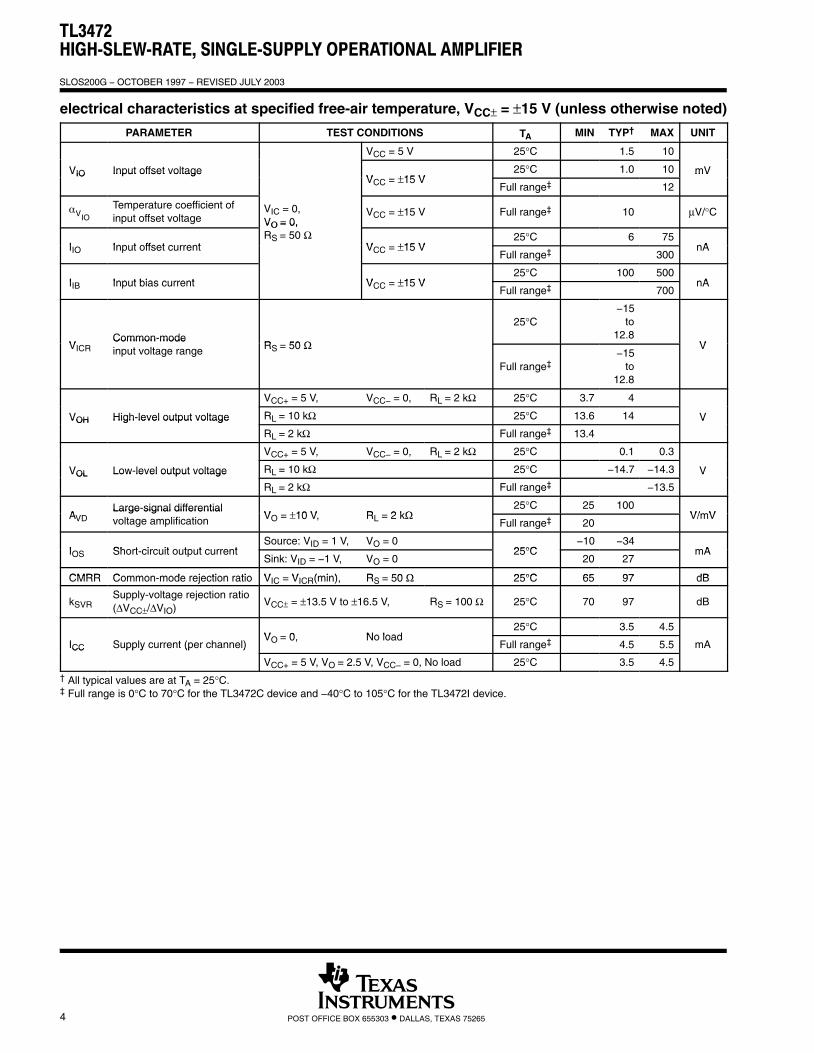
electrical characteristics at specified free-air temperature, VCC± = ±15 V (unless otherwise noted)
PARAMETER TEST CONDITIONS TA MIN TYP† MAX UNIT
VCC = 5 V 25°C 1.5 10
VIO Input offset voltageV ±15 V
25°C 1.0 10 mVVIO Input offset voltageVCC = ±15 V
Full range‡ 12
mV
�VIO
Temperature coefficient ofinput offset voltage
VIC = 0,VO = 0,
VCC = ±15 V Full range‡ 10 μV/°C
I Input offset current
VO = 0,RS = 50 Ω
V ±15 V25°C 6 75
nAIIO Input offset currentS
VCC = ±15 VFull range‡ 300
nA
I Input bias current V ±15 V25°C 100 500
nAIIB Input bias current VCC = ±15 VFull range‡ 700
nA
VCommon-mode
R 50 Ω
25°C−15
to12.8
VVICRCommon modeinput voltage range RS = 50 Ω
Full range‡−15
to12.8
V
VCC+ = 5 V, VCC− = 0, RL = 2 kΩ 25°C 3.7 4
VOH High-level output voltage RL = 10 kΩ 25°C 13.6 14 VVOH High level output voltage
RL = 2 kΩ Full range‡ 13.4
V
VCC+ = 5 V, VCC− = 0, RL = 2 kΩ 25°C 0.1 0.3
VOL Low-level output voltage RL = 10 kΩ 25°C −14.7 −14.3 VVOL Low level output voltage
RL = 2 kΩ Full range‡ −13.5
V
ALarge-signal differential
V ±10 V R 2 kΩ25°C 25 100
V/mVAVDLarge signal differentialvoltage amplification VO = ±10 V, RL = 2 kΩ
Full range‡ 20V/mV
I Short circuit output currentSource: VID = 1 V, VO = 0
25°C−10 −34
mAIOS Short-circuit output currentSink: VID = −1 V, VO = 0
25°C20 27
mA
CMRR Common mode rejection ratio V V (min) R 50 Ω 25°C 65 97 dBCMRR Common-mode rejection ratio VIC = VICR(min), RS = 50 Ω 25°C 65 97 dB
kSVRSupply-voltage rejection ratio(ΔVCC±/ΔVIO)
VCC± = ±13.5 V to ±16.5 V, RS = 100 Ω 25°C 70 97 dB
V 0 No load25°C 3.5 4.5
ICC Supply current (per channel)VO = 0, No load
Full range‡ 4.5 5.5 mACC pp y (p )
VCC+ = 5 V, VO = 2.5 V, VCC− = 0, No load 25°C 3.5 4.5† All typical values are at TA = 25°C.‡ Full range is 0°C to 70°C for the TL3472C device and −40°C to 105°C for the TL3472I device.
TL3472HIGH-SLEW-RATE, SINGLE-SUPPLY OPERATIONAL AMPLIFIER
SLOS200G − OCTOBER 1997 − REVISED JULY 2003
5POST OFFICE BOX 655303 • DALLAS, TEXAS 75265
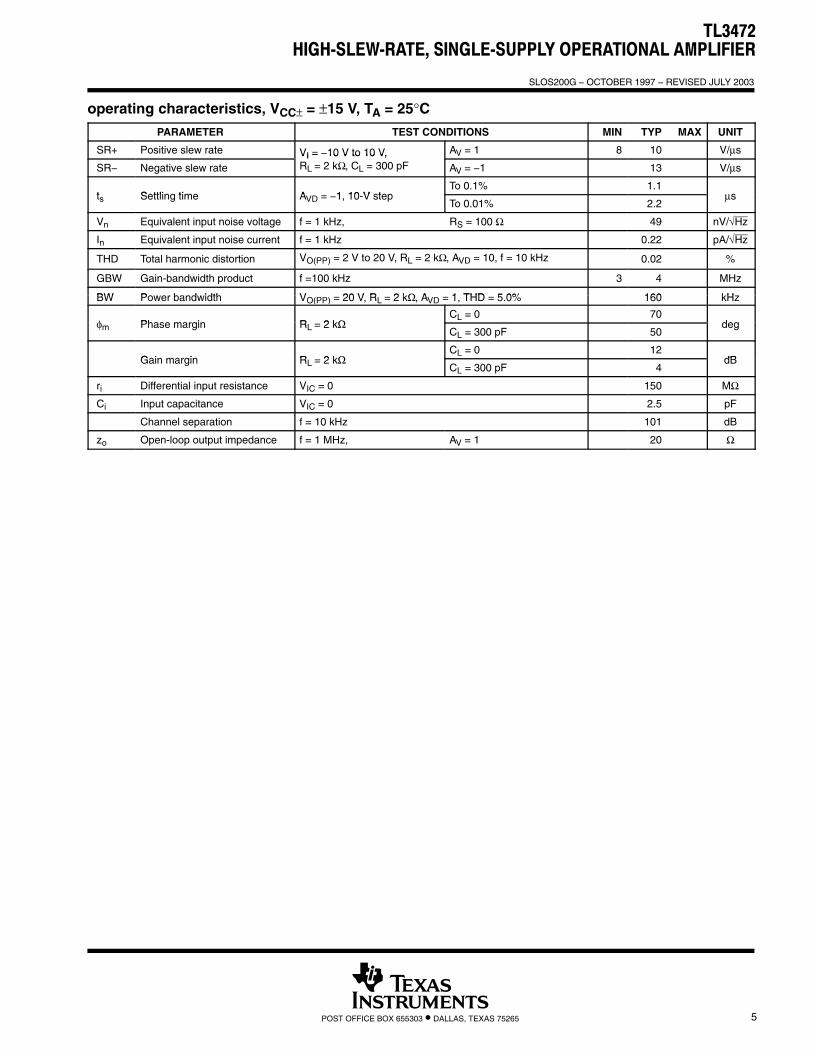
operating characteristics, VCC± = ±15 V, TA = 25°CPARAMETER TEST CONDITIONS MIN TYP MAX UNIT
SR+ Positive slew rate VI = −10 V to 10 V, AV = 1 8 10 V/μs
SR− Negative slew rate
VI = 10 V to 10 V,RL = 2 kΩ, CL = 300 pF AV = −1 13 V/μs
t Settling time A 1 10 V stepTo 0.1% 1.1
sts Settling time AVD = −1, 10-V stepTo 0.01% 2.2
μs
Vn Equivalent input noise voltage f = 1 kHz, RS = 100 Ω 49 nV/√Hz
In Equivalent input noise current f = 1 kHz 0.22 pA/√Hz
THD Total harmonic distortion VO(PP) = 2 V to 20 V, RL = 2 kΩ, AVD = 10, f = 10 kHz 0.02 %
GBW Gain-bandwidth product f =100 kHz 3 4 MHz
BW Power bandwidth V 20 V R 2 kΩ A 1 THD 5 0% 160 kHzBW Power bandwidth VO(PP) = 20 V, RL = 2 kΩ, AVD = 1, THD = 5.0% 160 kHz
φ Phase margin R 2 kΩCL = 0 70
degφm Phase margin RL = 2 kΩCL = 300 pF 50
deg
Gain margin R 2 kΩCL = 0 12
dBGain margin RL = 2 kΩCL = 300 pF 4
dB
ri Differential input resistance VIC = 0 150 MΩ
Ci Input capacitance VIC = 0 2.5 pF
Channel separation f = 10 kHz 101 dB
zo Open-loop output impedance f = 1 MHz, AV = 1 20 Ω
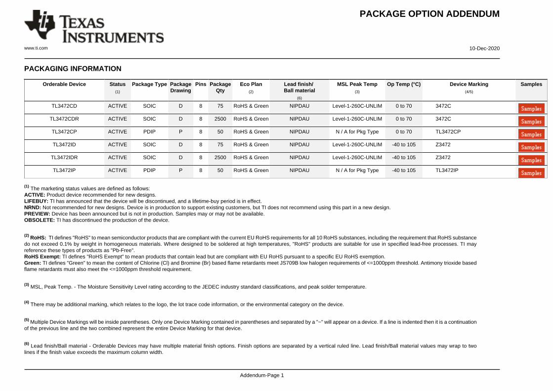
PACKAGE OPTION ADDENDUM
www.ti.com 10-Dec-2020
Addendum-Page 1
PACKAGING INFORMATION
Orderable Device Status(1)
Package Type PackageDrawing
Pins PackageQty
Eco Plan(2)
Lead finish/Ball material
(6)
MSL Peak Temp(3)
Op Temp (°C) Device Marking(4/5)
Samples
TL3472CD ACTIVE SOIC D 8 75 RoHS & Green NIPDAU Level-1-260C-UNLIM 0 to 70 3472C
TL3472CDR ACTIVE SOIC D 8 2500 RoHS & Green NIPDAU Level-1-260C-UNLIM 0 to 70 3472C
TL3472CP ACTIVE PDIP P 8 50 RoHS & Green NIPDAU N / A for Pkg Type 0 to 70 TL3472CP
TL3472ID ACTIVE SOIC D 8 75 RoHS & Green NIPDAU Level-1-260C-UNLIM -40 to 105 Z3472
TL3472IDR ACTIVE SOIC D 8 2500 RoHS & Green NIPDAU Level-1-260C-UNLIM -40 to 105 Z3472
TL3472IP ACTIVE PDIP P 8 50 RoHS & Green NIPDAU N / A for Pkg Type -40 to 105 TL3472IP
(1) The marketing status values are defined as follows:ACTIVE: Product device recommended for new designs.LIFEBUY: TI has announced that the device will be discontinued, and a lifetime-buy period is in effect.NRND: Not recommended for new designs. Device is in production to support existing customers, but TI does not recommend using this part in a new design.PREVIEW: Device has been announced but is not in production. Samples may or may not be available.OBSOLETE: TI has discontinued the production of the device.
(2) RoHS: TI defines "RoHS" to mean semiconductor products that are compliant with the current EU RoHS requirements for all 10 RoHS substances, including the requirement that RoHS substancedo not exceed 0.1% by weight in homogeneous materials. Where designed to be soldered at high temperatures, "RoHS" products are suitable for use in specified lead-free processes. TI mayreference these types of products as "Pb-Free".RoHS Exempt: TI defines "RoHS Exempt" to mean products that contain lead but are compliant with EU RoHS pursuant to a specific EU RoHS exemption.Green: TI defines "Green" to mean the content of Chlorine (Cl) and Bromine (Br) based flame retardants meet JS709B low halogen requirements of <=1000ppm threshold. Antimony trioxide basedflame retardants must also meet the <=1000ppm threshold requirement.
(3) MSL, Peak Temp. - The Moisture Sensitivity Level rating according to the JEDEC industry standard classifications, and peak solder temperature.
(4) There may be additional marking, which relates to the logo, the lot trace code information, or the environmental category on the device.
(5) Multiple Device Markings will be inside parentheses. Only one Device Marking contained in parentheses and separated by a "~" will appear on a device. If a line is indented then it is a continuationof the previous line and the two combined represent the entire Device Marking for that device.
(6) Lead finish/Ball material - Orderable Devices may have multiple material finish options. Finish options are separated by a vertical ruled line. Lead finish/Ball material values may wrap to twolines if the finish value exceeds the maximum column width.
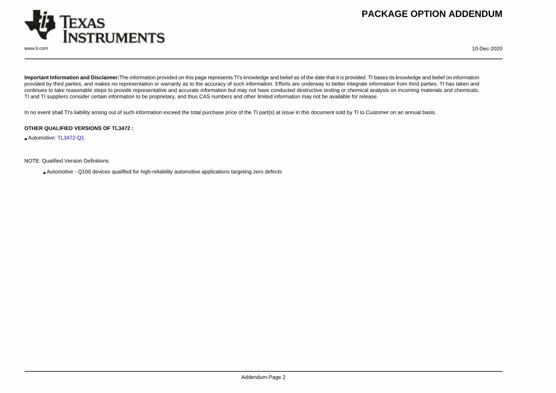
PACKAGE OPTION ADDENDUM
www.ti.com 10-Dec-2020
Addendum-Page 2
Important Information and Disclaimer:The information provided on this page represents TI's knowledge and belief as of the date that it is provided. TI bases its knowledge and belief on informationprovided by third parties, and makes no representation or warranty as to the accuracy of such information. Efforts are underway to better integrate information from third parties. TI has taken andcontinues to take reasonable steps to provide representative and accurate information but may not have conducted destructive testing or chemical analysis on incoming materials and chemicals.TI and TI suppliers consider certain information to be proprietary, and thus CAS numbers and other limited information may not be available for release.
In no event shall TI's liability arising out of such information exceed the total purchase price of the TI part(s) at issue in this document sold by TI to Customer on an annual basis.
OTHER QUALIFIED VERSIONS OF TL3472 :
• Automotive: TL3472-Q1
NOTE: Qualified Version Definitions:
• Automotive - Q100 devices qualified for high-reliability automotive applications targeting zero defects
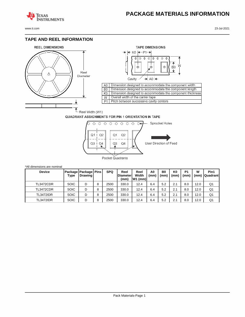
TAPE AND REEL INFORMATION
*All dimensions are nominal
Device PackageType
PackageDrawing
Pins SPQ ReelDiameter
(mm)
ReelWidth
W1 (mm)
A0(mm)
B0(mm)
K0(mm)
P1(mm)
W(mm)
Pin1Quadrant
TL3472CDR SOIC D 8 2500 330.0 12.4 6.4 5.2 2.1 8.0 12.0 Q1
TL3472CDR SOIC D 8 2500 330.0 12.4 6.4 5.2 2.1 8.0 12.0 Q1
TL3472IDR SOIC D 8 2500 330.0 12.4 6.4 5.2 2.1 8.0 12.0 Q1
TL3472IDR SOIC D 8 2500 330.0 12.4 6.4 5.2 2.1 8.0 12.0 Q1
PACKAGE MATERIALS INFORMATION
www.ti.com 23-Jul-2021
Pack Materials-Page 1
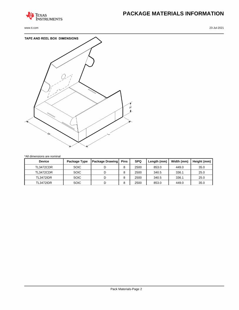
*All dimensions are nominal
Device Package Type Package Drawing Pins SPQ Length (mm) Width (mm) Height (mm)
TL3472CDR SOIC D 8 2500 853.0 449.0 35.0
TL3472CDR SOIC D 8 2500 340.5 336.1 25.0
TL3472IDR SOIC D 8 2500 340.5 336.1 25.0
TL3472IDR SOIC D 8 2500 853.0 449.0 35.0
PACKAGE MATERIALS INFORMATION
www.ti.com 23-Jul-2021
Pack Materials-Page 2
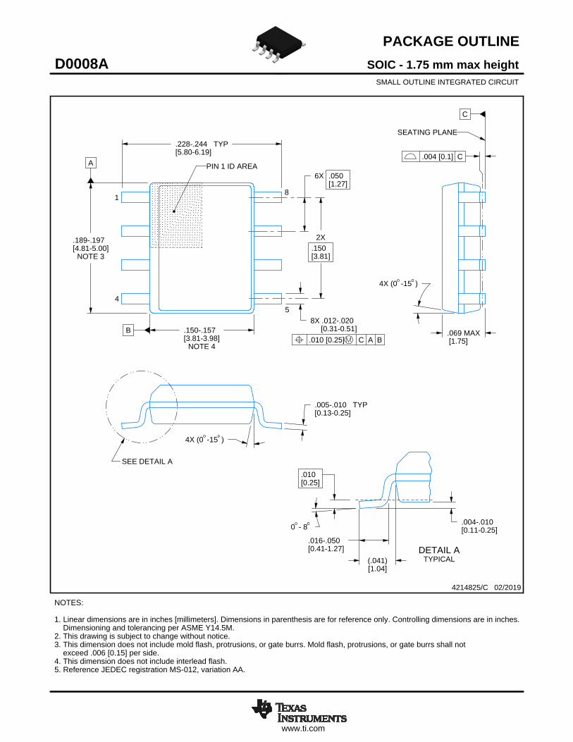
www.ti.com
PACKAGE OUTLINE
C
.228-.244 TYP[5.80-6.19]
.069 MAX[1.75]
6X .050[1.27]
8X .012-.020 [0.31-0.51]
2X.150[3.81]
.005-.010 TYP[0.13-0.25]
0 - 8 .004-.010[0.11-0.25]
.010[0.25]
.016-.050[0.41-1.27]
4X (0 -15 )
A
.189-.197[4.81-5.00]
NOTE 3
B .150-.157[3.81-3.98]
NOTE 4
4X (0 -15 )
(.041)[1.04]
SOIC - 1.75 mm max heightD0008ASMALL OUTLINE INTEGRATED CIRCUIT
4214825/C 02/2019
NOTES: 1. Linear dimensions are in inches [millimeters]. Dimensions in parenthesis are for reference only. Controlling dimensions are in inches. Dimensioning and tolerancing per ASME Y14.5M. 2. This drawing is subject to change without notice. 3. This dimension does not include mold flash, protrusions, or gate burrs. Mold flash, protrusions, or gate burrs shall not exceed .006 [0.15] per side. 4. This dimension does not include interlead flash.5. Reference JEDEC registration MS-012, variation AA.
18
.010 [0.25] C A B
54
PIN 1 ID AREA
SEATING PLANE
.004 [0.1] C
SEE DETAIL A
DETAIL ATYPICAL
SCALE 2.800
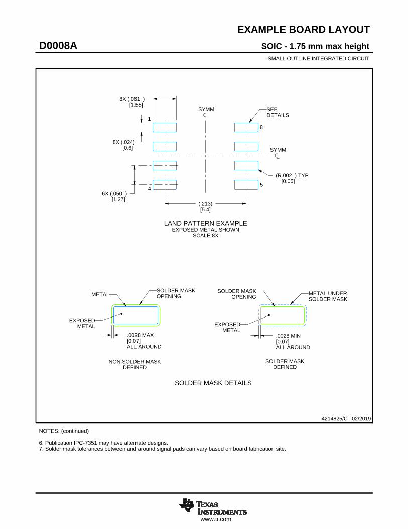
www.ti.com
EXAMPLE BOARD LAYOUT
.0028 MAX[0.07]ALL AROUND
.0028 MIN[0.07]ALL AROUND
(.213)[5.4]
6X (.050 )[1.27]
8X (.061 )[1.55]
8X (.024)[0.6]
(R.002 ) TYP[0.05]
SOIC - 1.75 mm max heightD0008ASMALL OUTLINE INTEGRATED CIRCUIT
4214825/C 02/2019
NOTES: (continued) 6. Publication IPC-7351 may have alternate designs. 7. Solder mask tolerances between and around signal pads can vary based on board fabrication site.
METALSOLDER MASKOPENING
NON SOLDER MASKDEFINED
SOLDER MASK DETAILS
EXPOSEDMETAL
OPENINGSOLDER MASK METAL UNDER
SOLDER MASK
SOLDER MASKDEFINED
EXPOSEDMETAL
LAND PATTERN EXAMPLEEXPOSED METAL SHOWN
SCALE:8X
SYMM
1
45
8
SEEDETAILS
SYMM
www.ti.com
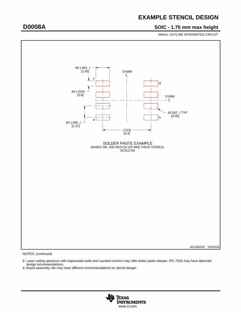
EXAMPLE STENCIL DESIGN
8X (.061 )[1.55]
8X (.024)[0.6]
6X (.050 )[1.27]
(.213)[5.4]
(R.002 ) TYP[0.05]
SOIC - 1.75 mm max heightD0008ASMALL OUTLINE INTEGRATED CIRCUIT
4214825/C 02/2019
NOTES: (continued) 8. Laser cutting apertures with trapezoidal walls and rounded corners may offer better paste release. IPC-7525 may have alternate design recommendations. 9. Board assembly site may have different recommendations for stencil design.
SOLDER PASTE EXAMPLEBASED ON .005 INCH [0.125 MM] THICK STENCIL
SCALE:8X
SYMM
SYMM
1
45
8
IMPORTANT NOTICE AND DISCLAIMERTI PROVIDES TECHNICAL AND RELIABILITY DATA (INCLUDING DATASHEETS), DESIGN RESOURCES (INCLUDING REFERENCEDESIGNS), APPLICATION OR OTHER DESIGN ADVICE, WEB TOOLS, SAFETY INFORMATION, AND OTHER RESOURCES “AS IS”AND WITH ALL FAULTS, AND DISCLAIMS ALL WARRANTIES, EXPRESS AND IMPLIED, INCLUDING WITHOUT LIMITATION ANYIMPLIED WARRANTIES OF MERCHANTABILITY, FITNESS FOR A PARTICULAR PURPOSE OR NON-INFRINGEMENT OF THIRDPARTY INTELLECTUAL PROPERTY RIGHTS.These resources are intended for skilled developers designing with TI products. You are solely responsible for (1) selecting the appropriateTI products for your application, (2) designing, validating and testing your application, and (3) ensuring your application meets applicablestandards, and any other safety, security, or other requirements. These resources are subject to change without notice. TI grants youpermission to use these resources only for development of an application that uses the TI products described in the resource. Otherreproduction and display of these resources is prohibited. No license is granted to any other TI intellectual property right or to any third partyintellectual property right. TI disclaims responsibility for, and you will fully indemnify TI and its representatives against, any claims, damages,costs, losses, and liabilities arising out of your use of these resources.TI’s products are provided subject to TI’s Terms of Sale (https:www.ti.com/legal/termsofsale.html) or other applicable terms available eitheron ti.com or provided in conjunction with such TI products. TI’s provision of these resources does not expand or otherwise alter TI’sapplicable warranties or warranty disclaimers for TI products.IMPORTANT NOTICE
Mailing Address: Texas Instruments, Post Office Box 655303, Dallas, Texas 75265Copyright © 2021, Texas Instruments Incorporated


![HIGH SPEED SINGLE SUPPLY OPERATIONAL AMPLIFIER · Ver. 02 [1] HIGH SPEED SINGLE SUPPLY OPERATIONAL AMPLIFIER FEATURES High Slew Rate 10V/µs High Bandwidth 3MHz High Unity Gain Frequency](https://img.pdfslide.net/doc/110x75/5fcebbdf2fae0d4d9a634fcd/high-speed-single-supply-operational-amplifier-ver-02-1-high-speed-single-supply.jpg)


![UNIT I: IC FABRICATION AND CIRCUIT CONFIGURATION FOR … · 13. Define slew rate. [AUC MAY 2011] The slew rate is defined as the maximum rate of change of output voltage causedby](https://img.pdfslide.net/doc/110x75/5e74613a16bf5842df045015/unit-i-ic-fabrication-and-circuit-configuration-for-13-define-slew-rate-auc.jpg)