Embed Size (px)
Citation preview
Product
Folder
Sample &Buy
Technical
Documents
Tools &
Software
Support &Community
An IMPORTANT NOTICE at the end of this data sheet addresses availability, warranty, changes, use in safety-critical applications,intellectual property matters and other important disclaimers. PRODUCTION DATA.
TL7702A, TL7705A, TL7709A, TL7712A, TL7715ASLVS028K –APRIL 1983–REVISED SEPTEMBER 2016
TL77xxA Supply-Voltage Supervisors
1
1 Features1• Power-On Reset Generator• Automatic Reset Generation After Voltage Drop• Wide Supply-Voltage Range• Precision Voltage Sensor• Temperature-Compensated Voltage Reference• Externally Adjustable Pulse Duration
2 Applications• Computers• Tablets• Smart Phones• Servers• Music Players
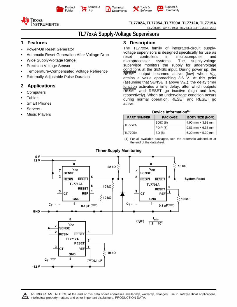
3 DescriptionThe TL77xxA family of integrated-circuit supply-voltage supervisors is designed specifically for use asreset controllers in microcomputer andmicroprocessor systems. The supply-voltagesupervisor monitors the supply for undervoltageconditions at the SENSE input. During power up, theRESET output becomes active (low) when VCCattains a value approaching 3.6 V. At this point(assuming that SENSE is above VIT+), the delay timerfunction activates a time delay, after which outputsRESET and RESET go inactive (high and low,respectively). When an undervoltage condition occursduring normal operation, RESET and RESET goactive.
Device Information(1)
PART NUMBER PACKAGE BODY SIZE (NOM)
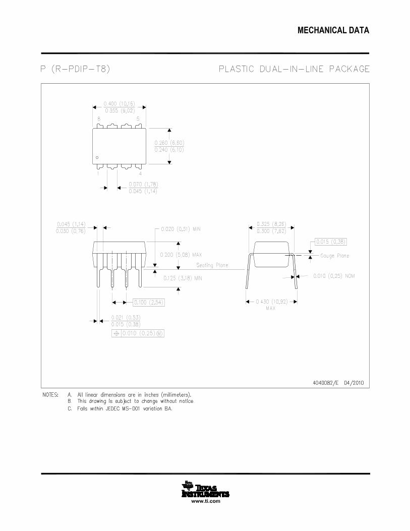
TL77xxASOIC (8) 4.90 mm × 3.91 mmPDIP (8) 9.81 mm × 6.35 mm
TL7705A SO (8) 6.20 mm × 5.30 mm
(1) For all available packages, see the orderable addendum atthe end of the datasheet.
Three-Supply Monitoring
2
TL7702A, TL7705A, TL7709A, TL7712A, TL7715ASLVS028K –APRIL 1983–REVISED SEPTEMBER 2016 www.ti.com
Product Folder Links: TL7702A TL7705A TL7709A TL7712A TL7715A
Submit Documentation Feedback Copyright © 1983–2016, Texas Instruments Incorporated
Table of Contents1 Features .................................................................. 12 Applications ........................................................... 13 Description ............................................................. 14 Revision History..................................................... 25 Pin Configuration and Functions ......................... 36 Specifications......................................................... 4
6.1 Absolute Maximum Ratings ...................................... 46.2 ESD Ratings.............................................................. 46.3 Recommended Operating Conditions....................... 46.4 Thermal Information .................................................. 56.5 Electrical Characteristics........................................... 56.6 Switching Characteristics .......................................... 56.7 Typical Characteristics .............................................. 6
7 Parameter Measurement Information .................. 78 Detailed Description .............................................. 8
8.1 Overview ................................................................... 88.2 Functional Block Diagram ......................................... 88.3 Feature Description................................................... 9
8.4 Device Functional Modes.......................................... 99 Application and Implementation ........................ 10
9.1 Application Information............................................ 109.2 Typical Application .................................................. 109.3 System Examples ................................................... 12
10 Power Supply Recommendations ..................... 1411 Layout................................................................... 14
11.1 Layout Guidelines ................................................. 1411.2 Layout Example .................................................... 14
12 Device and Documentation Support ................. 1512.1 Related Links ........................................................ 1512.2 Receiving Notification of Documentation Updates 1512.3 Community Resources.......................................... 1512.4 Trademarks ........................................................... 1512.5 Electrostatic Discharge Caution............................ 1512.6 Glossary ................................................................ 15
13 Mechanical, Packaging, and OrderableInformation ........................................................... 15
4 Revision HistoryNOTE: Page numbers for previous revisions may differ from page numbers in the current version.
Changes from Revision J (January 2015) to Revision K Page
• Added SO (8) to Device Information table.............................................................................................................................. 1• Changed RESET to RESET in Timing Diagram..................................................................................................................... 6• Added Receiving Notification of Documentation Updates section ....................................................................................... 15
Changes from Revision I (July 2009) to Revision J Page
• Added Applications, Device Information table, Pin Functions table, ESD Ratings table, Thermal Information table,Typical Characteristics, Feature Description section, Device Functional Modes, Application and Implementationsection, Power Supply Recommendations section, Layout section, Device and Documentation Support section, andMechanical, Packaging, and Orderable Information section. ................................................................................................. 1
• Deleted Ordering Information table. ....................................................................................................................................... 1
1REF 8 VCC
2RESIN 7 SENSE
3CT 6 RESET
4GND 5 RESET
Not to scale
3
TL7702A, TL7705A, TL7709A, TL7712A, TL7715Awww.ti.com SLVS028K –APRIL 1983–REVISED SEPTEMBER 2016
Product Folder Links: TL7702A TL7705A TL7709A TL7712A TL7715A
Submit Documentation FeedbackCopyright © 1983–2016, Texas Instruments Incorporated
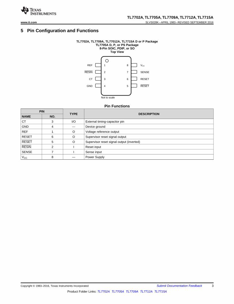
5 Pin Configuration and Functions
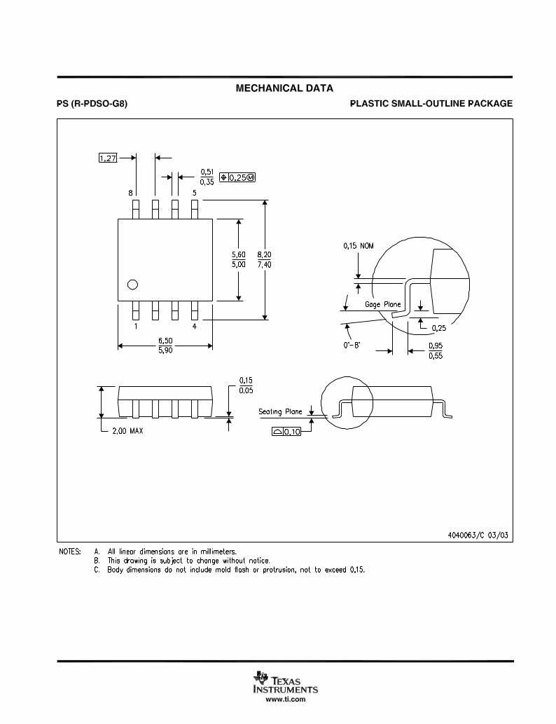
TL7702A, TL7709A, TL77012A, TL7715A D or P PackageTL7705A D, P, or PS Package
8-Pin SOIC, PDIP, or SOTop View
Pin FunctionsPIN
TYPE DESCRIPTIONNAME NO.CT 3 I/O External timing-capacitor pinGND 4 — Device groundREF 1 O Voltage reference outputRESET 6 O Supervisor reset signal outputRESET 5 O Supervisor reset signal output (inverted)RESIN 2 I Reset inputSENSE 7 I Sense inputVCC 8 — Power Supply
4
TL7702A, TL7705A, TL7709A, TL7712A, TL7715ASLVS028K –APRIL 1983–REVISED SEPTEMBER 2016 www.ti.com
Product Folder Links: TL7702A TL7705A TL7709A TL7712A TL7715A
Submit Documentation Feedback Copyright © 1983–2016, Texas Instruments Incorporated
(1) Stresses beyond those listed under Absolute Maximum Ratings may cause permanent damage to the device. These are stress ratingsonly, which do not imply functional operation of the device at these or any other conditions beyond those indicated under RecommendedOperating Conditions. Exposure to absolute-maximum-rated conditions for extended periods may affect device reliability.
(2) For proper operation of the TL7702A, the voltage applied to the SENSE terminal should not exceed VCC − 1 V or 6 V, whichever is less(3) All voltage values are with respect to GND.
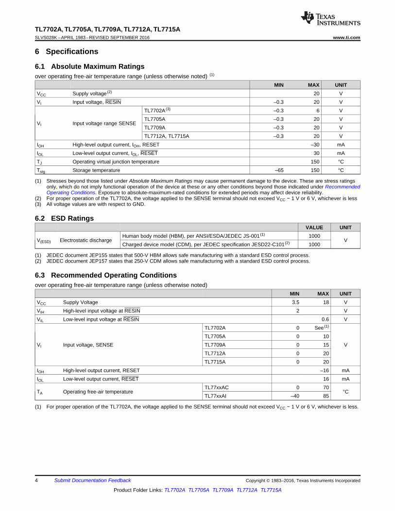
6 Specifications
6.1 Absolute Maximum Ratingsover operating free-air temperature range (unless otherwise noted) (1)
MIN MAX UNITVCC Supply voltage (2) 20 VVI Input voltage, RESIN –0.3 20 V
VI Input voltage range SENSE
TL7702A (3) –0.3 6 VTL7705A –0.3 20 VTL7709A –0.3 20 VTL7712A, TL7715A –0.3 20 V
IOH High-level output current, IOH, RESET –30 mAIOL Low-level output current, IOL, RESET 30 mATJ Operating virtual junction temperature 150 °CTstg Storage temperature –65 150 °C
(1) JEDEC document JEP155 states that 500-V HBM allows safe manufacturing with a standard ESD control process.(2) JEDEC document JEP157 states that 250-V CDM allows safe manufacturing with a standard ESD control process.
6.2 ESD RatingsVALUE UNIT
V(ESD) Electrostatic dischargeHuman body model (HBM), per ANSI/ESDA/JEDEC JS-001 (1) 1000
VCharged device model (CDM), per JEDEC specification JESD22-C101 (2) 1000
(1) For proper operation of the TL7702A, the voltage applied to the SENSE terminal should not exceed VCC − 1 V or 6 V, whichever is less.
6.3 Recommended Operating Conditionsover operating free-air temperature range (unless otherwise noted)
MIN MAX UNITVCC Supply Voltage 3.5 18 VVIH High-level input voltage at RESIN 2 VVIL Low-level input voltage at RESIN 0.6 V
VI Input voltage, SENSE
TL7702A 0 See (1)
VTL7705A 0 10TL7709A 0 15TL7712A 0 20TL7715A 0 20
IOH High-level output current, RESET –16 mAIOL Low-level output current, RESET 16 mA
TA Operating free-air temperatureTL77xxAC 0 70
°CTL77xxAI –40 85

5
TL7702A, TL7705A, TL7709A, TL7712A, TL7715Awww.ti.com SLVS028K –APRIL 1983–REVISED SEPTEMBER 2016
Product Folder Links: TL7702A TL7705A TL7709A TL7712A TL7715A
Submit Documentation FeedbackCopyright © 1983–2016, Texas Instruments Incorporated
(1) For more information about traditional and new thermal metrics, see the Semiconductor and IC Package Thermal Metrics applicationreport.
6.4 Thermal Information
THERMAL METRIC (1)TL77xxA
UNITD P PS8 PINS 8 PINS 8 PINS
RθJA Junction-to-ambient thermal resistance 97 85 95 °C/W
(1) All electrical characteristics are measured with 0.1-µF capacitors connected at REF, CT, and VCC to GND.
6.5 Electrical Characteristicsover operating free-air temperature range (unless otherwise noted)
PARAMETER TEST CONDITIONS (1)TL77xxACTL77xxAI UNIT
MIN TYP MAX
VOH High-level output voltage, RESET IOH = –16 mA VCC – 1.5 V
VOL Low-level output voltage, RESET IOL = 16 mA 0.4 V
Vref Reference Voltage TA = 25°C 2.48 2.53 2.58 V
VIT–Negative-going inputthreshold voltage, SENSE
TL7702A
TA = 25°C
2.48 2.53 2.58
V
TL7705A 4.5 4.55 4.6
TL7709A 7.5 7.6 7.7
TL7712A 10.6 10.8 11
TL7715A 13.2 13.5 13.8
VhysHysteresis, SENS (VIT+ –VIT–)
TL7702A
TA = 25°C
10
mV
TL7705A 15
TL7709A 20
TL7712A 35
TL7715A 45
II Input currentRESIN
VI = 2.4 V to VCC 20
µAVI = 0.4 V –100
SENSE TL7702A Vref < VI < VCC – 1.5 V 0.5 2
IOH High-level output current, RESET VO = 18 V 50 µA
IOL Low-level output current, RESET VO = 0 –50 µA
ICC Supply current All inputs and outputs open 1.8 3 mA
(1) All switching characteristics are measured with 0.1-µF capacitors connected at REF and VCC to GND.(2) The rise and fall times are measured with a 4.7-kΩ load resistor at RESET and RESET.
6.6 Switching Characteristicsover operating free-air temperature range (unless otherwise noted)
PARAMETER TEST CONDITIONS (1)TL77xxACTL77xxAI UNIT
MIN TYP MAX
Output pulse duration CT = 0.1 µF 0.65 1.2 2.6 msec
Input pulse duration at RESIN 0.4 µs
tw(S)Pulse duration at sense input to switchoutputs
VIH = VIT− + 200 mV, VIL = VIT− − 200mV 2 µs
tpd propagation delay time, RESIN to RESET VCC = 5V 1 µs
tr Rise timeRESET
VCC = 5 V (2) 0.2µs
RESET 3.5
tf Fall timeRESET
VCC = 5 V (2) 3.5µs
RESET 0.2
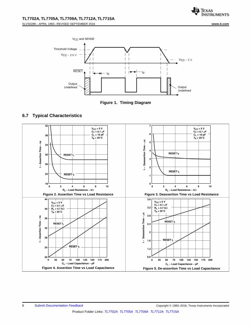
~ 2 V
~ 3.6 V
RESET
OutputUndefined
VCC and SENSE
Threshold Voltage
VCC
tdtd
VCC
OutputUndefined
6
TL7702A, TL7705A, TL7709A, TL7712A, TL7715ASLVS028K –APRIL 1983–REVISED SEPTEMBER 2016 www.ti.com
Product Folder Links: TL7702A TL7705A TL7709A TL7712A TL7715A
Submit Documentation Feedback Copyright © 1983–2016, Texas Instruments Incorporated
Figure 1. Timing Diagram
6.7 Typical Characteristics
Figure 2. Assertion Time vs Load Resistance Figure 3. Deassertion Time vs Load Resistance
Figure 4. Assertion Time vs Load Capacitance Figure 5. De-assertion Time vs Load Capacitance
7
TL7702A, TL7705A, TL7709A, TL7712A, TL7715Awww.ti.com SLVS028K –APRIL 1983–REVISED SEPTEMBER 2016
Product Folder Links: TL7702A TL7705A TL7709A TL7712A TL7715A
Submit Documentation FeedbackCopyright © 1983–2016, Texas Instruments Incorporated
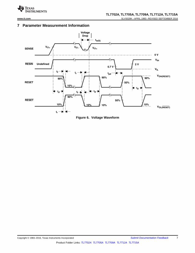
7 Parameter Measurement Information
Figure 6. Voltage Waveform
~100 µA
8
TL7702A, TL7705A, TL7709A, TL7712A, TL7715ASLVS028K –APRIL 1983–REVISED SEPTEMBER 2016 www.ti.com
Product Folder Links: TL7702A TL7705A TL7709A TL7712A TL7715A
Submit Documentation Feedback Copyright © 1983–2016, Texas Instruments Incorporated
8 Detailed Description
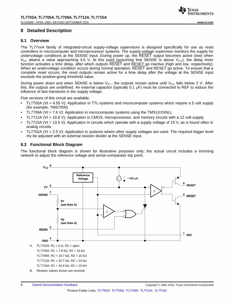
8.1 OverviewThe TL77xxA family of integrated-circuit supply-voltage supervisors is designed specifically for use as resetcontrollers in microcomputer and microprocessor systems. The supply-voltage supervisor monitors the supply forundervoltage conditions at the SENSE input. During power up, the RESET output becomes active (low) whenVCC attains a value approaching 3.6 V. At this point (assuming that SENSE is above VIT+), the delay timerfunction activates a time delay, after which outputs RESET and RESET go inactive (high and low, respectively).When an undervoltage condition occurs during normal operation, RESET and RESET go active. To ensure that acomplete reset occurs, the reset outputs remain active for a time delay after the voltage at the SENSE inputexceeds the positive-going threshold value.
During power down and when SENSE is below VIT−, the outputs remain active until VCC falls below 2 V. Afterthis, the outputs are undefined. An external capacitor (typically 0.1 μF) must be connected to REF to reduce theinfluence of fast transients in the supply voltage.
Five versions of this circuit are available:• TL7705A (Vt = 4.55 V): Application in TTL-systems and microcomputer systems which require a 5 volt supply
(for example, TMS7000)• TL7709A (Vt = 7.6 V): Application in microcomputer systems using the TMS1XXXNLL• TL7712A (Vt = 10.8 V): Application in CMOS, microprocessor, and memory circuits with a 12 volt supply.• TL7715A (Vt = 13.5 V): Application in circuits which operate with a supply voltage of 15 V, as is found often in
analog circuits.• TL7702A (Vt = 2.5 V): Application in systems where other supply voltages are used. The required trigger level
my be adjusted with an external resistor divider at the SENSE input.
8.2 Functional Block DiagramThe functional block diagram is shown for illustrative purposes only; the actual circuit includes a trimmingnetwork to adjust the reference voltage and sense-comparator trip point.
A. TL7702A: R1 = 0 Ω, R2 = openTL7705A: R1 = 7.8 kΩ, R2 = 10 kΩTL7709A: R1 = 19.7 kΩ, R2 = 10 kΩTL7712A: R1 = 32.7 kΩ, R2 = 10 kΩTL7715A: R1 = 43.4 kΩ, R2 = 10 kΩ
B. Resistor values shown are nominal.
9
TL7702A, TL7705A, TL7709A, TL7712A, TL7715Awww.ti.com SLVS028K –APRIL 1983–REVISED SEPTEMBER 2016
Product Folder Links: TL7702A TL7705A TL7709A TL7712A TL7715A
Submit Documentation FeedbackCopyright © 1983–2016, Texas Instruments Incorporated
8.3 Feature Description
8.3.1 Wide Supply-Voltage RangeTh TL77xxA family operates of a wide supply voltage range of 3.5 V to 18 V.
8.3.2 Externally Adjustable Pulse DurationThe time delay is determined by the value of the external capacitor CT: td = 1.3 × 10⁴ × CT, where CT is in farads(F) and td is in seconds (s).
8.3.3 Temperature-Compensated Voltage ReferenceThe series TL77xxA incorporates an extremely stable reference voltage source. This voltage source can also beused in applications where a constant voltage source is required. The reference voltage varies less than 10 mVover the supply voltage range of 3.5 V to 18 V. The same stability of the reference voltage is maintained, whenthe ambient temperature is changed. The reference's voltage varies only 16 mV when the ambient temperature ischanged from –40°C to +85°C.
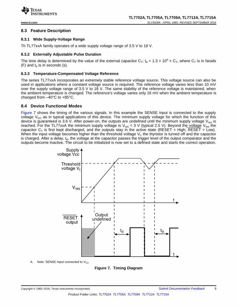
8.4 Device Functional ModesFigure 7 shows the timing of the various signals. In this example the SENSE input is connected to the supplyvoltage VCC as in typical applications of this device. The minimum supply voltage for which the function of thisdevice is guaranteed is 3.6 V. After power-on, the outputs are undefined until the minimum supply voltage Vres isreached. For the TL77xxA the minimum supply voltage is Vres = 3 V (typical 2.5 V). Beyond the voltage Vres thecapacitor CT is first kept discharged, and the outputs stay in the active state (RESET = High, RESET = Low).When the input voltage becomes higher than the threshold voltage Vt, the thyristor is turned off and the capacitoris charged. After a delay, td, the voltage at the capacitor passes the trigger level of the output comparator and theoutputs become inactive. The circuit to be initialized is now set to a defined state and starts the correct operation.
A. Note: SENSE Input connected to VCC
Figure 7. Timing Diagram
=
µC
10
TL7702A, TL7705A, TL7709A, TL7712A, TL7715ASLVS028K –APRIL 1983–REVISED SEPTEMBER 2016 www.ti.com
Product Folder Links: TL7702A TL7705A TL7709A TL7712A TL7715A
Submit Documentation Feedback Copyright © 1983–2016, Texas Instruments Incorporated
9 Application and Implementation
NOTEInformation in the following applications sections is not part of the TI componentspecification, and TI does not warrant its accuracy or completeness. TI’s customers areresponsible for determining suitability of components for their purposes. Customers shouldvalidate and test their design implementation to confirm system functionality.
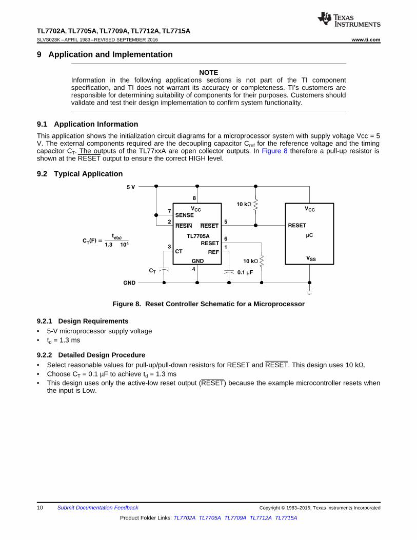
9.1 Application InformationThis application shows the initialization circuit diagrams for a microprocessor system with supply voltage Vcc = 5V. The external components required are the decoupling capacitor Cref for the reference voltage and the timingcapacitor CT. The outputs of the TL77xxA are open collector outputs. In Figure 8 therefore a pull-up resistor isshown at the RESET output to ensure the correct HIGH level.
9.2 Typical Application
Figure 8. Reset Controller Schematic for a Microprocessor
9.2.1 Design Requirements• 5-V microprocessor supply voltage• td = 1.3 ms
9.2.2 Detailed Design Procedure• Select reasonable values for pull-up/pull-down resistors for RESET and RESET. This design uses 10 kΩ.• Choose CT = 0.1 µF to achieve td = 1.3 ms• This design uses only the active-low reset output (RESET) because the example microcontroller resets when
the input is Low.
VCC (V)
RE
SE
T V
olta
ge (
V)
4.5 4.52 4.54 4.56 4.58 4.60
0.5
1
1.5
2
2.5
3
3.5
4
4.5
5
D007VCC (V)
RE
SE
T V
olta
ge (
V)
4.5 4.52 4.54 4.56 4.58 4.60
0.5
1
1.5
2
2.5
3
3.5
4
4.5
5
D008
VCC (V)
RE
SE
T V
olta
ge (
V)
0 0.5 1 1.5 2 2.5 3 3.5 4 4.5 50
0.5
1
1.5
2
2.5
3
3.5
4
4.5
5
D005VCC (V)
RE
SE
T V
olta
ge (
V)
0 0.5 1 1.5 2 2.5 3 3.5 4 4.5 50
0.5
1
1.5
2
2.5
3
3.5
4
4.5
5
D006
11
TL7702A, TL7705A, TL7709A, TL7712A, TL7715Awww.ti.com SLVS028K –APRIL 1983–REVISED SEPTEMBER 2016
Product Folder Links: TL7702A TL7705A TL7709A TL7712A TL7715A
Submit Documentation FeedbackCopyright © 1983–2016, Texas Instruments Incorporated
Typical Application (continued)9.2.3 Application Curves
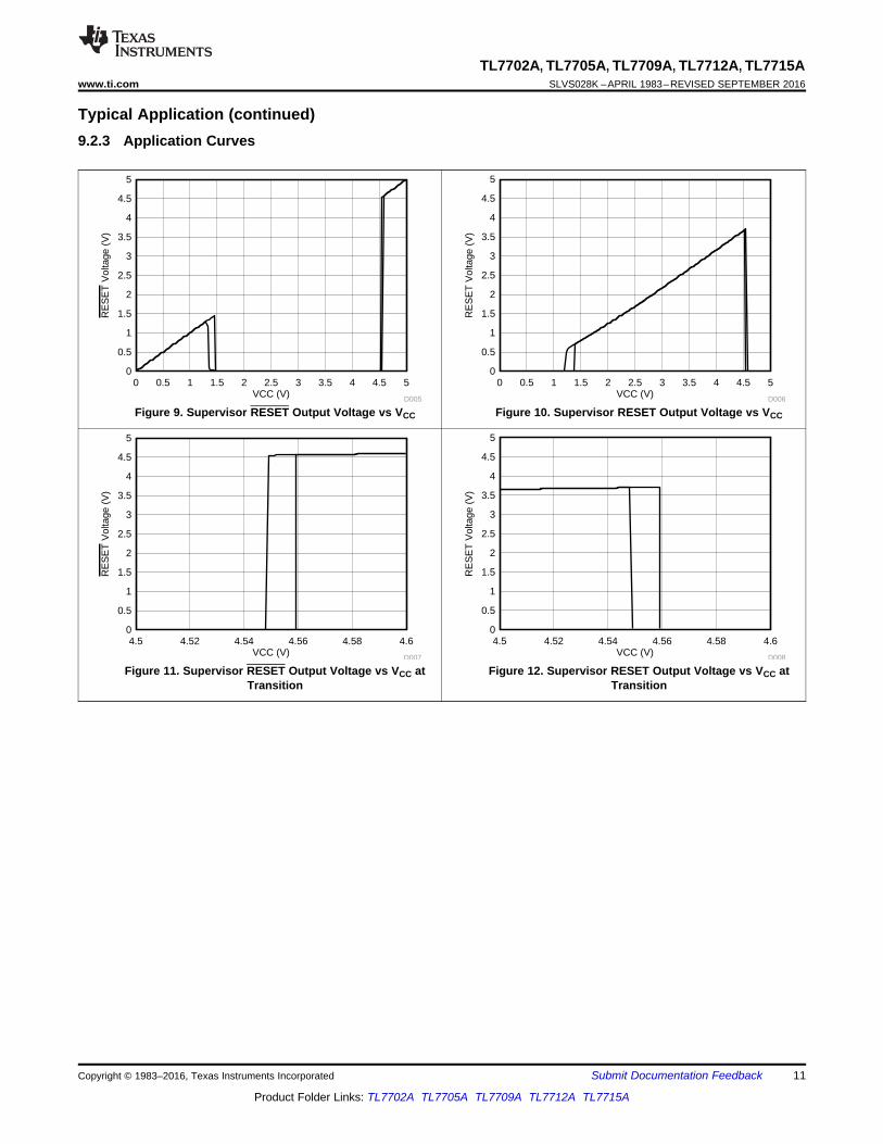
Figure 9. Supervisor RESET Output Voltage vs VCC Figure 10. Supervisor RESET Output Voltage vs VCC
Figure 11. Supervisor RESET Output Voltage vs VCC atTransition
Figure 12. Supervisor RESET Output Voltage vs VCC atTransition

12
TL7702A, TL7705A, TL7709A, TL7712A, TL7715ASLVS028K –APRIL 1983–REVISED SEPTEMBER 2016 www.ti.com
Product Folder Links: TL7702A TL7705A TL7709A TL7712A TL7715A
Submit Documentation Feedback Copyright © 1983–2016, Texas Instruments Incorporated
9.3 System Examples
Figure 13. Multi Power-Supply System Reset Generation Schematic
Figure 14. Eliminating Undefined States Using a P-Channel JFET Schematic
13
TL7702A, TL7705A, TL7709A, TL7712A, TL7715Awww.ti.com SLVS028K –APRIL 1983–REVISED SEPTEMBER 2016
Product Folder Links: TL7702A TL7705A TL7709A TL7712A TL7715A
Submit Documentation FeedbackCopyright © 1983–2016, Texas Instruments Incorporated
System Examples (continued)
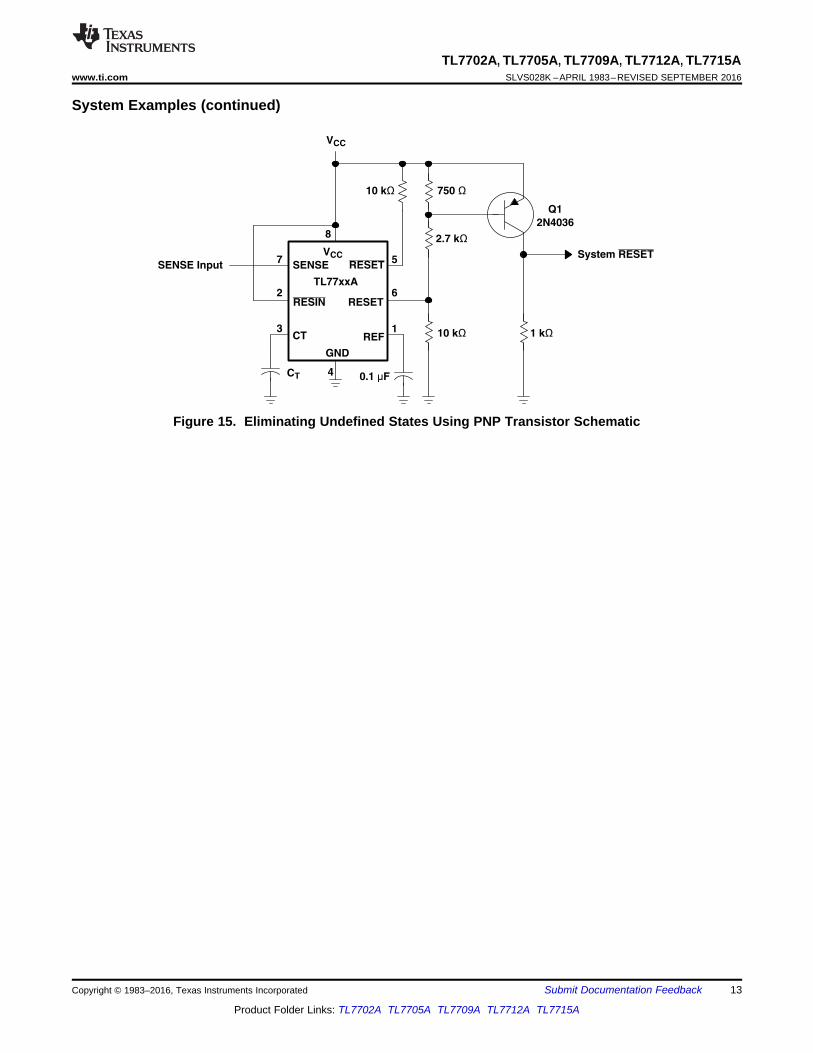
Figure 15. Eliminating Undefined States Using PNP Transistor Schematic
1
2
3
4
8
7
6
5
14
TL7702A, TL7705A, TL7709A, TL7712A, TL7715ASLVS028K –APRIL 1983–REVISED SEPTEMBER 2016 www.ti.com
Product Folder Links: TL7702A TL7705A TL7709A TL7712A TL7715A
Submit Documentation Feedback Copyright © 1983–2016, Texas Instruments Incorporated
10 Power Supply RecommendationsThe TL77xxA devices operate within the specifications from the Recommended Operating Conditions between3.5 V and 18 V.
CAUTIONThese devices risk being damaged when powered by more than 20 V.
11 Layout
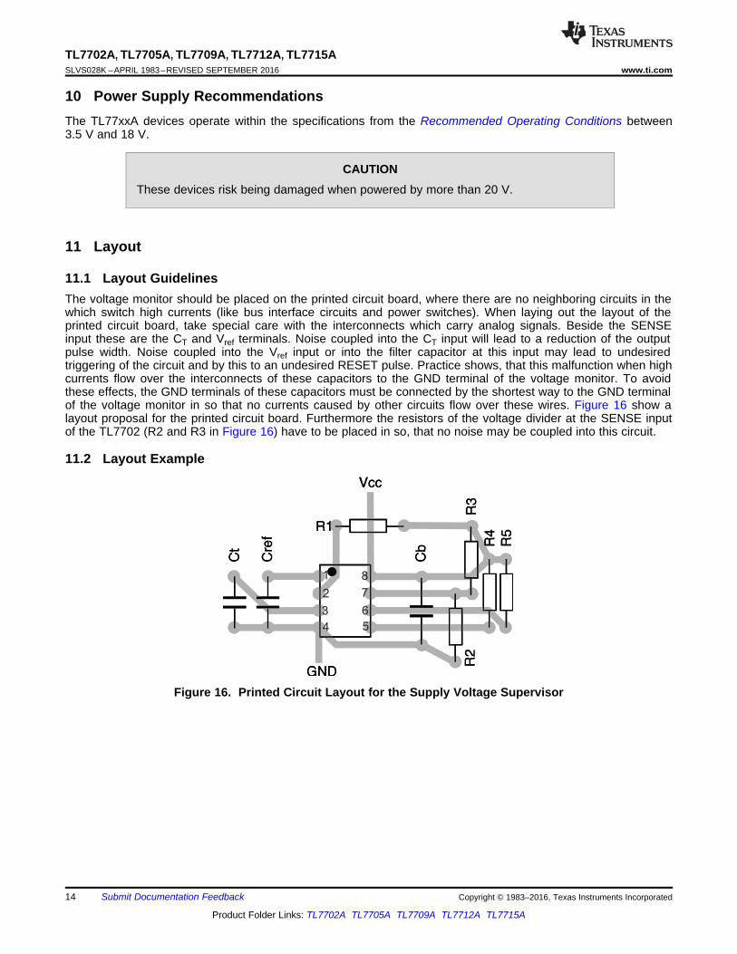
11.1 Layout GuidelinesThe voltage monitor should be placed on the printed circuit board, where there are no neighboring circuits in thewhich switch high currents (like bus interface circuits and power switches). When laying out the layout of theprinted circuit board, take special care with the interconnects which carry analog signals. Beside the SENSEinput these are the CT and Vref terminals. Noise coupled into the CT input will lead to a reduction of the outputpulse width. Noise coupled into the Vref input or into the filter capacitor at this input may lead to undesiredtriggering of the circuit and by this to an undesired RESET pulse. Practice shows, that this malfunction when highcurrents flow over the interconnects of these capacitors to the GND terminal of the voltage monitor. To avoidthese effects, the GND terminals of these capacitors must be connected by the shortest way to the GND terminalof the voltage monitor in so that no currents caused by other circuits flow over these wires. Figure 16 show alayout proposal for the printed circuit board. Furthermore the resistors of the voltage divider at the SENSE inputof the TL7702 (R2 and R3 in Figure 16) have to be placed in so, that no noise may be coupled into this circuit.
11.2 Layout Example
Figure 16. Printed Circuit Layout for the Supply Voltage Supervisor

15
TL7702A, TL7705A, TL7709A, TL7712A, TL7715Awww.ti.com SLVS028K –APRIL 1983–REVISED SEPTEMBER 2016
Product Folder Links: TL7702A TL7705A TL7709A TL7712A TL7715A
Submit Documentation FeedbackCopyright © 1983–2016, Texas Instruments Incorporated
12 Device and Documentation Support
12.1 Related LinksThe table below lists quick access links. Categories include technical documents, support and communityresources, tools and software, and quick access to sample or buy.
Table 1. Related Links
PARTS PRODUCT FOLDER SAMPLE & BUY TECHNICALDOCUMENTS
TOOLS &SOFTWARE
SUPPORT &COMMUNITY
TL7702A Click here Click here Click here Click here Click hereTL7705A Click here Click here Click here Click here Click hereTL7709A Click here Click here Click here Click here Click hereTL7712A Click here Click here Click here Click here Click hereTL7715A Click here Click here Click here Click here Click here
12.2 Receiving Notification of Documentation UpdatesTo receive notification of documentation updates, navigate to the device product folder on ti.com. In the upperright corner, click on Alert me to register and receive a weekly digest of any product information that haschanged. For change details, review the revision history included in any revised document.
12.3 Community ResourcesThe following links connect to TI community resources. Linked contents are provided "AS IS" by the respectivecontributors. They do not constitute TI specifications and do not necessarily reflect TI's views; see TI's Terms ofUse.
TI E2E™ Online Community TI's Engineer-to-Engineer (E2E) Community. Created to foster collaborationamong engineers. At e2e.ti.com, you can ask questions, share knowledge, explore ideas and helpsolve problems with fellow engineers.
Design Support TI's Design Support Quickly find helpful E2E forums along with design support tools andcontact information for technical support.
12.4 TrademarksE2E is a trademark of Texas Instruments.All other trademarks are the property of their respective owners.
12.5 Electrostatic Discharge CautionThis integrated circuit can be damaged by ESD. Texas Instruments recommends that all integrated circuits be handled withappropriate precautions. Failure to observe proper handling and installation procedures can cause damage.
ESD damage can range from subtle performance degradation to complete device failure. Precision integrated circuits may be moresusceptible to damage because very small parametric changes could cause the device not to meet its published specifications.
12.6 GlossarySLYZ022 — TI Glossary.
This glossary lists and explains terms, acronyms, and definitions.
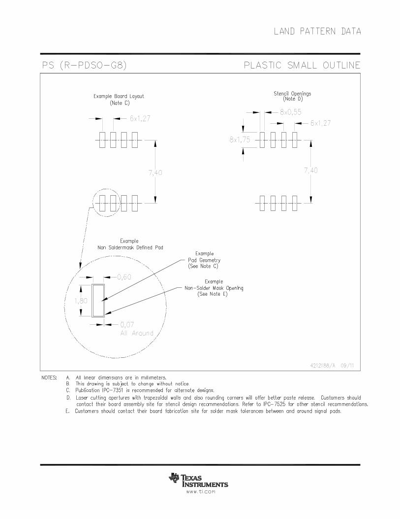
13 Mechanical, Packaging, and Orderable InformationThe following pages include mechanical, packaging, and orderable information. This information is the mostcurrent data available for the designated devices. This data is subject to change without notice and revision ofthis document. For browser-based versions of this data sheet, refer to the left-hand navigation.
PACKAGE OPTION ADDENDUM
www.ti.com 14-Aug-2021
Addendum-Page 1
PACKAGING INFORMATION
Orderable Device Status(1)
Package Type PackageDrawing
Pins PackageQty
Eco Plan(2)
Lead finish/Ball material
(6)
MSL Peak Temp(3)
Op Temp (°C) Device Marking(4/5)
Samples
TL7702ACD ACTIVE SOIC D 8 75 RoHS & Green NIPDAU Level-1-260C-UNLIM 0 to 70 7702AC
TL7702ACDR ACTIVE SOIC D 8 2500 RoHS & Green NIPDAU Level-1-260C-UNLIM 0 to 70 7702AC
TL7702ACDRG4 ACTIVE SOIC D 8 2500 RoHS & Green NIPDAU Level-1-260C-UNLIM 0 to 70 7702AC
TL7702ACP ACTIVE PDIP P 8 50 RoHS & Green NIPDAU N / A for Pkg Type 0 to 70 TL7702ACP
TL7702AID ACTIVE SOIC D 8 75 RoHS & Green NIPDAU Level-1-260C-UNLIM -40 to 85 7702AI
TL7702AIDR ACTIVE SOIC D 8 2500 RoHS & Green NIPDAU Level-1-260C-UNLIM -40 to 85 7702AI
TL7702AIDRG4 ACTIVE SOIC D 8 2500 RoHS & Green NIPDAU Level-1-260C-UNLIM -40 to 85 7702AI
TL7702AIP ACTIVE PDIP P 8 50 RoHS & Green NIPDAU N / A for Pkg Type -40 to 85 TL7702AIP
TL7702AIPE4 ACTIVE PDIP P 8 50 RoHS & Green NIPDAU N / A for Pkg Type -40 to 85 TL7702AIP
TL7705ACD ACTIVE SOIC D 8 75 RoHS & Green NIPDAU Level-1-260C-UNLIM 0 to 70 7705AC
TL7705ACDE4 ACTIVE SOIC D 8 75 RoHS & Green NIPDAU Level-1-260C-UNLIM 0 to 70 7705AC
TL7705ACDG4 ACTIVE SOIC D 8 75 RoHS & Green NIPDAU Level-1-260C-UNLIM 0 to 70 7705AC
TL7705ACDR ACTIVE SOIC D 8 2500 RoHS & Green NIPDAU Level-1-260C-UNLIM 0 to 70 7705AC
TL7705ACDRG4 ACTIVE SOIC D 8 2500 RoHS & Green NIPDAU Level-1-260C-UNLIM 0 to 70 7705AC
TL7705ACP ACTIVE PDIP P 8 50 RoHS & Green NIPDAU N / A for Pkg Type 0 to 70 TL7705ACP
TL7705ACPE4 ACTIVE PDIP P 8 50 RoHS & Green NIPDAU N / A for Pkg Type 0 to 70 TL7705ACP
TL7705ACPSR ACTIVE SO PS 8 2000 RoHS & Green NIPDAU Level-1-260C-UNLIM 0 to 70 T7705A
TL7705AID ACTIVE SOIC D 8 75 RoHS & Green NIPDAU Level-1-260C-UNLIM -40 to 85 7705AI
TL7705AIDG4 ACTIVE SOIC D 8 75 RoHS & Green NIPDAU Level-1-260C-UNLIM -40 to 85 7705AI
TL7705AIDR ACTIVE SOIC D 8 2500 RoHS & Green NIPDAU Level-1-260C-UNLIM -40 to 85 7705AI
PACKAGE OPTION ADDENDUM
www.ti.com 14-Aug-2021
Addendum-Page 2
Orderable Device Status(1)
Package Type PackageDrawing
Pins PackageQty
Eco Plan(2)
Lead finish/Ball material
(6)
MSL Peak Temp(3)
Op Temp (°C) Device Marking(4/5)
Samples
TL7705AIDRG4 ACTIVE SOIC D 8 2500 RoHS & Green NIPDAU Level-1-260C-UNLIM -40 to 85 7705AI
TL7705AIP ACTIVE PDIP P 8 50 RoHS & Green NIPDAU N / A for Pkg Type -40 to 85 TL7705AIP
TL7709ACD ACTIVE SOIC D 8 75 RoHS & Green NIPDAU Level-1-260C-UNLIM 0 to 70 7709AC
TL7709ACDG4 ACTIVE SOIC D 8 75 RoHS & Green NIPDAU Level-1-260C-UNLIM 0 to 70 7709AC
TL7709ACDR ACTIVE SOIC D 8 2500 RoHS & Green NIPDAU Level-1-260C-UNLIM 0 to 70 7709AC
TL7709ACP ACTIVE PDIP P 8 50 RoHS & Green NIPDAU N / A for Pkg Type 0 to 70 TL7709ACP
TL7712ACD ACTIVE SOIC D 8 75 RoHS & Green NIPDAU Level-1-260C-UNLIM 0 to 70 7712AC
TL7712ACDE4 ACTIVE SOIC D 8 75 RoHS & Green NIPDAU Level-1-260C-UNLIM 0 to 70 7712AC
TL7712ACDG4 ACTIVE SOIC D 8 75 RoHS & Green NIPDAU Level-1-260C-UNLIM 0 to 70 7712AC
TL7712ACDR ACTIVE SOIC D 8 2500 RoHS & Green NIPDAU Level-1-260C-UNLIM 0 to 70 7712AC
TL7712ACDRE4 ACTIVE SOIC D 8 2500 RoHS & Green NIPDAU Level-1-260C-UNLIM 0 to 70 7712AC
TL7712ACDRG4 ACTIVE SOIC D 8 2500 RoHS & Green NIPDAU Level-1-260C-UNLIM 0 to 70 7712AC
TL7712ACP ACTIVE PDIP P 8 50 RoHS & Green NIPDAU N / A for Pkg Type 0 to 70 TL7712ACP
TL7712AIDR ACTIVE SOIC D 8 2500 RoHS & Green NIPDAU Level-1-260C-UNLIM 7712AI
TL7715ACD ACTIVE SOIC D 8 75 RoHS & Green NIPDAU Level-1-260C-UNLIM 0 to 70 7715AC
TL7715ACDE4 ACTIVE SOIC D 8 75 RoHS & Green NIPDAU Level-1-260C-UNLIM 0 to 70 7715AC
TL7715ACP ACTIVE PDIP P 8 50 RoHS & Green NIPDAU N / A for Pkg Type 0 to 70 TL7715ACP
(1) The marketing status values are defined as follows:ACTIVE: Product device recommended for new designs.LIFEBUY: TI has announced that the device will be discontinued, and a lifetime-buy period is in effect.NRND: Not recommended for new designs. Device is in production to support existing customers, but TI does not recommend using this part in a new design.PREVIEW: Device has been announced but is not in production. Samples may or may not be available.OBSOLETE: TI has discontinued the production of the device.
PACKAGE OPTION ADDENDUM
www.ti.com 14-Aug-2021
Addendum-Page 3
(2) RoHS: TI defines "RoHS" to mean semiconductor products that are compliant with the current EU RoHS requirements for all 10 RoHS substances, including the requirement that RoHS substancedo not exceed 0.1% by weight in homogeneous materials. Where designed to be soldered at high temperatures, "RoHS" products are suitable for use in specified lead-free processes. TI mayreference these types of products as "Pb-Free".RoHS Exempt: TI defines "RoHS Exempt" to mean products that contain lead but are compliant with EU RoHS pursuant to a specific EU RoHS exemption.Green: TI defines "Green" to mean the content of Chlorine (Cl) and Bromine (Br) based flame retardants meet JS709B low halogen requirements of <=1000ppm threshold. Antimony trioxide basedflame retardants must also meet the <=1000ppm threshold requirement.
(3) MSL, Peak Temp. - The Moisture Sensitivity Level rating according to the JEDEC industry standard classifications, and peak solder temperature.
(4) There may be additional marking, which relates to the logo, the lot trace code information, or the environmental category on the device.
(5) Multiple Device Markings will be inside parentheses. Only one Device Marking contained in parentheses and separated by a "~" will appear on a device. If a line is indented then it is a continuationof the previous line and the two combined represent the entire Device Marking for that device.
(6) Lead finish/Ball material - Orderable Devices may have multiple material finish options. Finish options are separated by a vertical ruled line. Lead finish/Ball material values may wrap to twolines if the finish value exceeds the maximum column width.
Important Information and Disclaimer:The information provided on this page represents TI's knowledge and belief as of the date that it is provided. TI bases its knowledge and belief on informationprovided by third parties, and makes no representation or warranty as to the accuracy of such information. Efforts are underway to better integrate information from third parties. TI has taken andcontinues to take reasonable steps to provide representative and accurate information but may not have conducted destructive testing or chemical analysis on incoming materials and chemicals.TI and TI suppliers consider certain information to be proprietary, and thus CAS numbers and other limited information may not be available for release.
In no event shall TI's liability arising out of such information exceed the total purchase price of the TI part(s) at issue in this document sold by TI to Customer on an annual basis.
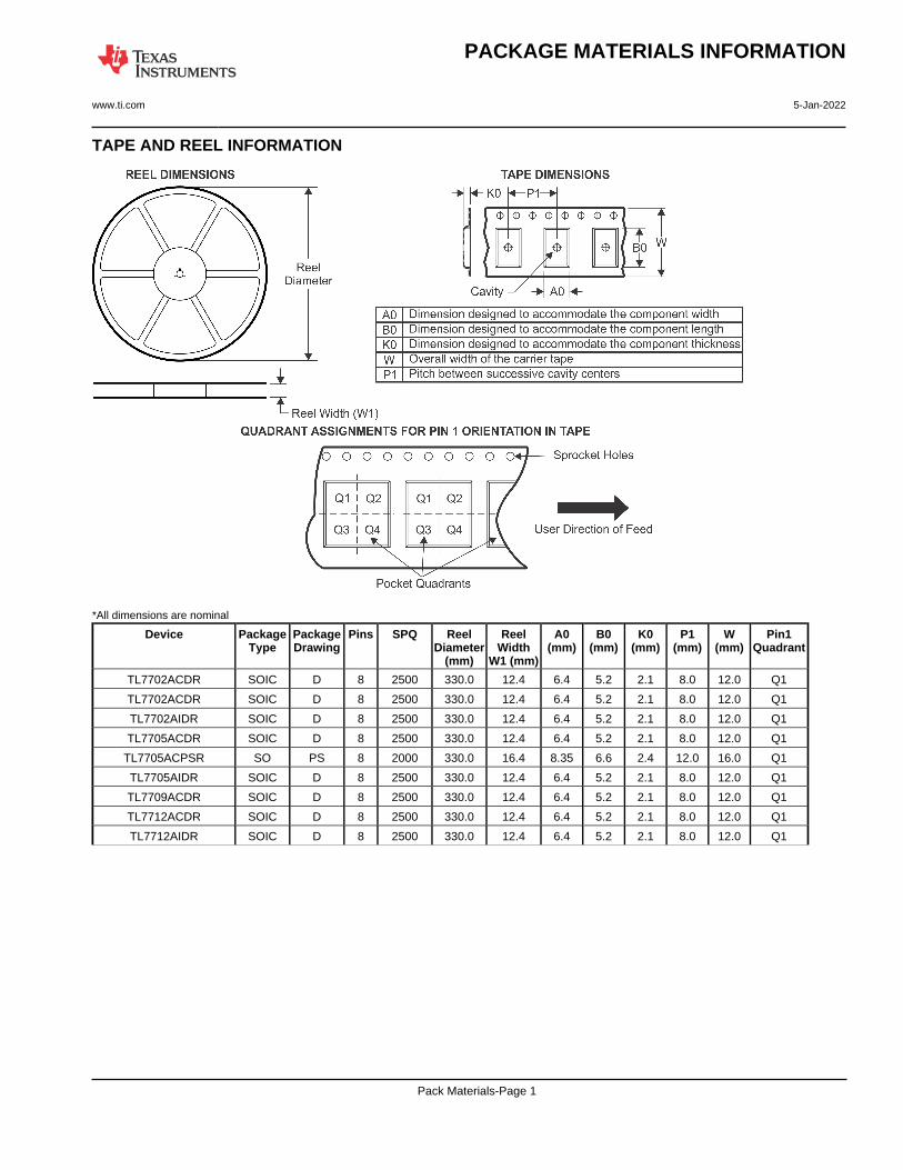
TAPE AND REEL INFORMATION
*All dimensions are nominal
Device PackageType
PackageDrawing
Pins SPQ ReelDiameter
(mm)
ReelWidth
W1 (mm)
A0(mm)
B0(mm)
K0(mm)
P1(mm)
W(mm)
Pin1Quadrant
TL7702ACDR SOIC D 8 2500 330.0 12.4 6.4 5.2 2.1 8.0 12.0 Q1
TL7702ACDR SOIC D 8 2500 330.0 12.4 6.4 5.2 2.1 8.0 12.0 Q1
TL7702AIDR SOIC D 8 2500 330.0 12.4 6.4 5.2 2.1 8.0 12.0 Q1
TL7705ACDR SOIC D 8 2500 330.0 12.4 6.4 5.2 2.1 8.0 12.0 Q1
TL7705ACPSR SO PS 8 2000 330.0 16.4 8.35 6.6 2.4 12.0 16.0 Q1
TL7705AIDR SOIC D 8 2500 330.0 12.4 6.4 5.2 2.1 8.0 12.0 Q1
TL7709ACDR SOIC D 8 2500 330.0 12.4 6.4 5.2 2.1 8.0 12.0 Q1
TL7712ACDR SOIC D 8 2500 330.0 12.4 6.4 5.2 2.1 8.0 12.0 Q1
TL7712AIDR SOIC D 8 2500 330.0 12.4 6.4 5.2 2.1 8.0 12.0 Q1
PACKAGE MATERIALS INFORMATION
www.ti.com 5-Jan-2022
Pack Materials-Page 1

*All dimensions are nominal
Device Package Type Package Drawing Pins SPQ Length (mm) Width (mm) Height (mm)
TL7702ACDR SOIC D 8 2500 340.5 336.1 25.0
TL7702ACDR SOIC D 8 2500 853.0 449.0 35.0
TL7702AIDR SOIC D 8 2500 340.5 336.1 25.0
TL7705ACDR SOIC D 8 2500 340.5 336.1 25.0
TL7705ACPSR SO PS 8 2000 853.0 449.0 35.0
TL7705AIDR SOIC D 8 2500 340.5 336.1 25.0
TL7709ACDR SOIC D 8 2500 340.5 336.1 25.0
TL7712ACDR SOIC D 8 2500 340.5 336.1 25.0
TL7712AIDR SOIC D 8 2500 340.5 336.1 25.0
PACKAGE MATERIALS INFORMATION
www.ti.com 5-Jan-2022
Pack Materials-Page 2
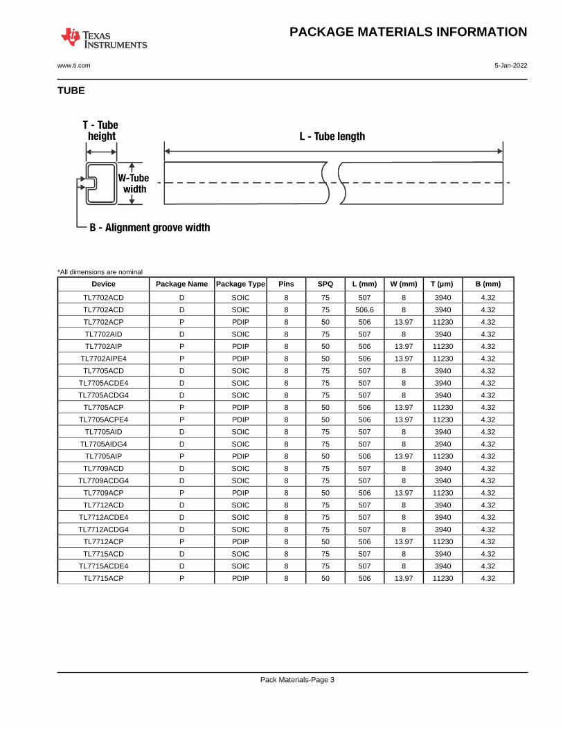
TUBE
*All dimensions are nominal
Device Package Name Package Type Pins SPQ L (mm) W (mm) T (µm) B (mm)
TL7702ACD D SOIC 8 75 507 8 3940 4.32
TL7702ACD D SOIC 8 75 506.6 8 3940 4.32
TL7702ACP P PDIP 8 50 506 13.97 11230 4.32
TL7702AID D SOIC 8 75 507 8 3940 4.32
TL7702AIP P PDIP 8 50 506 13.97 11230 4.32
TL7702AIPE4 P PDIP 8 50 506 13.97 11230 4.32
TL7705ACD D SOIC 8 75 507 8 3940 4.32
TL7705ACDE4 D SOIC 8 75 507 8 3940 4.32
TL7705ACDG4 D SOIC 8 75 507 8 3940 4.32
TL7705ACP P PDIP 8 50 506 13.97 11230 4.32
TL7705ACPE4 P PDIP 8 50 506 13.97 11230 4.32
TL7705AID D SOIC 8 75 507 8 3940 4.32
TL7705AIDG4 D SOIC 8 75 507 8 3940 4.32
TL7705AIP P PDIP 8 50 506 13.97 11230 4.32
TL7709ACD D SOIC 8 75 507 8 3940 4.32
TL7709ACDG4 D SOIC 8 75 507 8 3940 4.32
TL7709ACP P PDIP 8 50 506 13.97 11230 4.32
TL7712ACD D SOIC 8 75 507 8 3940 4.32
TL7712ACDE4 D SOIC 8 75 507 8 3940 4.32
TL7712ACDG4 D SOIC 8 75 507 8 3940 4.32
TL7712ACP P PDIP 8 50 506 13.97 11230 4.32
TL7715ACD D SOIC 8 75 507 8 3940 4.32
TL7715ACDE4 D SOIC 8 75 507 8 3940 4.32
TL7715ACP P PDIP 8 50 506 13.97 11230 4.32
PACKAGE MATERIALS INFORMATION
www.ti.com 5-Jan-2022
Pack Materials-Page 3
www.ti.com
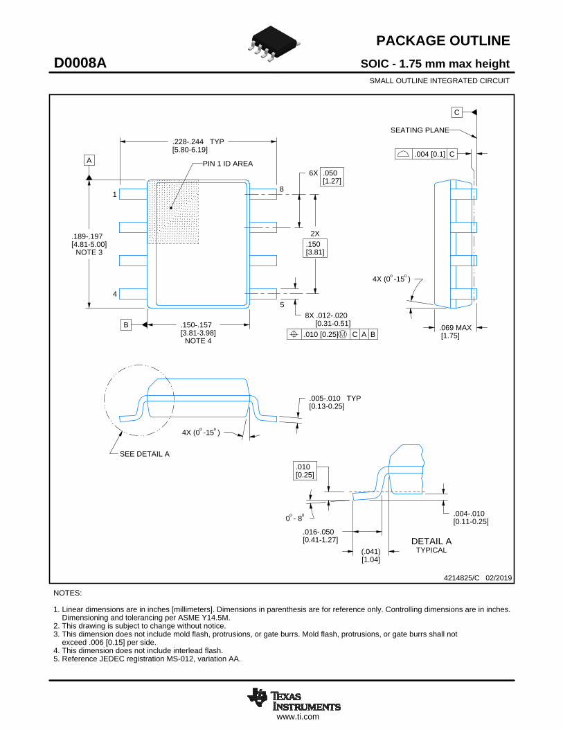
PACKAGE OUTLINE
C
.228-.244 TYP[5.80-6.19]
.069 MAX[1.75]
6X .050[1.27]
8X .012-.020 [0.31-0.51]
2X.150[3.81]
.005-.010 TYP[0.13-0.25]
0 - 8 .004-.010[0.11-0.25]
.010[0.25]
.016-.050[0.41-1.27]
4X (0 -15 )
A
.189-.197[4.81-5.00]
NOTE 3
B .150-.157[3.81-3.98]
NOTE 4
4X (0 -15 )
(.041)[1.04]
SOIC - 1.75 mm max heightD0008ASMALL OUTLINE INTEGRATED CIRCUIT
4214825/C 02/2019
NOTES: 1. Linear dimensions are in inches [millimeters]. Dimensions in parenthesis are for reference only. Controlling dimensions are in inches. Dimensioning and tolerancing per ASME Y14.5M. 2. This drawing is subject to change without notice. 3. This dimension does not include mold flash, protrusions, or gate burrs. Mold flash, protrusions, or gate burrs shall not exceed .006 [0.15] per side. 4. This dimension does not include interlead flash.5. Reference JEDEC registration MS-012, variation AA.
18
.010 [0.25] C A B
54
PIN 1 ID AREA
SEATING PLANE
.004 [0.1] C
SEE DETAIL A
DETAIL ATYPICAL
SCALE 2.800

www.ti.com
EXAMPLE BOARD LAYOUT
.0028 MAX[0.07]ALL AROUND
.0028 MIN[0.07]ALL AROUND
(.213)[5.4]
6X (.050 )[1.27]
8X (.061 )[1.55]
8X (.024)[0.6]
(R.002 ) TYP[0.05]
SOIC - 1.75 mm max heightD0008ASMALL OUTLINE INTEGRATED CIRCUIT
4214825/C 02/2019
NOTES: (continued) 6. Publication IPC-7351 may have alternate designs. 7. Solder mask tolerances between and around signal pads can vary based on board fabrication site.
METALSOLDER MASKOPENING
NON SOLDER MASKDEFINED
SOLDER MASK DETAILS
EXPOSEDMETAL
OPENINGSOLDER MASK METAL UNDER
SOLDER MASK
SOLDER MASKDEFINED
EXPOSEDMETAL
LAND PATTERN EXAMPLEEXPOSED METAL SHOWN
SCALE:8X
SYMM
1
45
8
SEEDETAILS
SYMM

www.ti.com
EXAMPLE STENCIL DESIGN
8X (.061 )[1.55]
8X (.024)[0.6]
6X (.050 )[1.27]
(.213)[5.4]
(R.002 ) TYP[0.05]
SOIC - 1.75 mm max heightD0008ASMALL OUTLINE INTEGRATED CIRCUIT
4214825/C 02/2019
NOTES: (continued) 8. Laser cutting apertures with trapezoidal walls and rounded corners may offer better paste release. IPC-7525 may have alternate design recommendations. 9. Board assembly site may have different recommendations for stencil design.
SOLDER PASTE EXAMPLEBASED ON .005 INCH [0.125 MM] THICK STENCIL
SCALE:8X
SYMM
SYMM
1
45
8
IMPORTANT NOTICE AND DISCLAIMERTI PROVIDES TECHNICAL AND RELIABILITY DATA (INCLUDING DATA SHEETS), DESIGN RESOURCES (INCLUDING REFERENCE DESIGNS), APPLICATION OR OTHER DESIGN ADVICE, WEB TOOLS, SAFETY INFORMATION, AND OTHER RESOURCES “AS IS” AND WITH ALL FAULTS, AND DISCLAIMS ALL WARRANTIES, EXPRESS AND IMPLIED, INCLUDING WITHOUT LIMITATION ANY IMPLIED WARRANTIES OF MERCHANTABILITY, FITNESS FOR A PARTICULAR PURPOSE OR NON-INFRINGEMENT OF THIRD PARTY INTELLECTUAL PROPERTY RIGHTS.These resources are intended for skilled developers designing with TI products. You are solely responsible for (1) selecting the appropriate TI products for your application, (2) designing, validating and testing your application, and (3) ensuring your application meets applicable standards, and any other safety, security, regulatory or other requirements.These resources are subject to change without notice. TI grants you permission to use these resources only for development of an application that uses the TI products described in the resource. Other reproduction and display of these resources is prohibited. No license is granted to any other TI intellectual property right or to any third party intellectual property right. TI disclaims responsibility for, and you will fully indemnify TI and its representatives against, any claims, damages, costs, losses, and liabilities arising out of your use of these resources.TI’s products are provided subject to TI’s Terms of Sale or other applicable terms available either on ti.com or provided in conjunction with such TI products. TI’s provision of these resources does not expand or otherwise alter TI’s applicable warranties or warranty disclaimers for TI products.TI objects to and rejects any additional or different terms you may have proposed. IMPORTANT NOTICE
Mailing Address: Texas Instruments, Post Office Box 655303, Dallas, Texas 75265Copyright © 2022, Texas Instruments Incorporated