Embed Size (px)
Citation preview
TLV702-Q1
GNDEN
IN OUTVIN VOUT
On
Off
CIN1 �FCeramicCOUT
Product
Folder
Order
Now
Technical
Documents
Tools &
Software
Support &Community
An IMPORTANT NOTICE at the end of this data sheet addresses availability, warranty, changes, use in safety-critical applications,intellectual property matters and other important disclaimers. PRODUCTION DATA.
TLV702-Q1SLVSC35D –AUGUST 2013–REVISED JULY 2019
TLV702-Q1 300-mA, Low-IQ, Low-Dropout Regulator
1
1 Features1• Qualified for Automotive Applications• AEC-Q100 Qualified with the Following Results:
– Device Temperature Grade 1: –40°C to 125°CAmbient Operating Temperature Range
– Device HBM ESD Classification Level H2– Device CDM ESD Classification Level C4B
• Very Low Dropout:– 37 mV at IOUT = 50 mA, VOUT = 2.8 V– 75 mV at IOUT = 100 mA, VOUT = 2.8 V– 220 mV at IOUT = 300 mA, VOUT = 2.8 V
• 2% Accuracy Over Temperature• Low IQ: 35 µA• Fixed-Output Voltage Combinations Possible from
1.2 V to 4.8 V• High PSRR: 68 dB at 1 kHz• Stable with Effective Capacitance of 0.1 µF(1)
• Thermal Shutdown and Overcurrent Protection• Packages: 5-Pin SOT (DBV and DDC) and
1.5-mm × 1.5-mm, 6-Pin WSON(1) See the Input and Output Capacitor Requirements in the
Application Information section.
2 Applications• Automotive Camera Modules• Image Sensor Power• Microprocessor Rails• Automotive Infotainment Head Units• Automotive Body Electronics
3 DescriptionThe TLV702-Q1 series of low-dropout (LDO) linearregulators are low quiescent current devices withexcellent line and load transient performance. TheseLDOs are designed for power-sensitive applications.
A precision bandgap and an error amplifier provideoverall 2% accuracy. Low output noise, very highpower-supply rejection ratio (PSRR), and low-dropoutvoltage make this series of devices ideal for a wideselection of battery-operated equipment. All deviceversions have thermal shutdown and current limitprotections for safety.
Furthermore, these devices are stable with aneffective output capacitance of only 0.1 µF. Thisfeature enables the use of cost-effective capacitorsthat have higher bias voltages and temperaturederating. The devices regulate to specified accuracywith no output load.
The TLV702-Q1 series of LDO linear regulators isavailable in SOT and WSON packages.
Device Information(1)
PART NUMBER PACKAGE BODY SIZE (NOM)
TLV702-Q1SOT (5) 2.90 mm × 1.60 mmWSON (6) 1.50 mm × 1.50 mm
(1) For all available packages, see the package option addendumat the end of the data sheet.
Typical Application
2
TLV702-Q1SLVSC35D –AUGUST 2013–REVISED JULY 2019 www.ti.com
Product Folder Links: TLV702-Q1
Submit Documentation Feedback Copyright © 2013–2019, Texas Instruments Incorporated
Table of Contents1 Features .................................................................. 12 Applications ........................................................... 13 Description ............................................................. 14 Revision History..................................................... 25 Pin Configuration and Functions ......................... 46 Specifications......................................................... 5
6.1 Absolute Maximum Ratings ...................................... 56.2 ESD Ratings.............................................................. 56.3 Recommended Operating Conditions....................... 56.4 Thermal Information .................................................. 56.5 Electrical Characteristics........................................... 66.6 Typical Characteristics .............................................. 7
7 Detailed Description ............................................ 117.1 Overview ................................................................. 117.2 Functional Block Diagrams ..................................... 117.3 Feature Description................................................. 117.4 Device Functional Modes........................................ 12
8 Application and Implementation ........................ 138.1 Application Information............................................ 138.2 Typical Application .................................................. 13
9 Power Supply Recommendations ...................... 159.1 Power Dissipation ................................................... 15
10 Layout................................................................... 1510.1 Layout Guidelines ................................................. 1510.2 Layout Examples................................................... 16
11 Device and Documentation Support ................. 1711.1 Device Support .................................................... 1711.2 Documentation Support ........................................ 1711.3 Receiving Notification of Documentation Updates 1711.4 Community Resources.......................................... 1711.5 Trademarks ........................................................... 1711.6 Electrostatic Discharge Caution............................ 1711.7 Glossary ................................................................ 18
12 Mechanical, Packaging, and OrderableInformation ........................................................... 18
4 Revision HistoryNOTE: Page numbers for previous revisions may differ from page numbers in the current version.
Changes from Revision C (January 2018) to Revision D Page
• Changed OUT pin number from 5 to 3 in DSE column of Pin Functions table ..................................................................... 4• Added footnote to maximum EN voltage specification .......................................................................................................... 5• Added parameter names to Recommended Operating Conditions table............................................................................... 5
Changes from Revision B (June 2015) to Revision C Page
• Added DBV package to document ......................................................................................................................................... 1• Changed Packages Features bullet to include DBV package ............................................................................................... 1• Added DBV package to Pin Configuration and Functions section ......................................................................................... 4• Added DBV column to Thermal Information table .................................................................................................................. 5• Changed title of Layout Example for the DDC and DBV Packages figure to include DBV package ................................... 16
Changes from Revision A (August 2013) to Revision B Page
• Added DSE (6-Pin WSON) package to data sheet ................................................................................................................ 1• Added Device Information, ESD Ratings, and Recommended Operating Conditions tables, and Detailed
Description, Application and Implementation, Power Supply Recommendations, Layout, Device and DocumentationSupport, and Mechanical, Packaging, and Orderable Information sections to data sheet .................................................... 1
• Deleted all references to P version of device throughout data sheet..................................................................................... 1• Added "Over Temperature" to 2% accuracy Features bullet ................................................................................................ 1• Changed DDC package name from TSOT23 to SOT throughout data sheet........................................................................ 1• Changed Applications bullets ................................................................................................................................................. 1• Changed Description section text........................................................................................................................................... 1• Changed ceramic capacitor units on Typical Application circuit from mF to µF (typo) ......................................................... 1• Changed "free-air temperature" to "junction temperature" in Absolute Maximum Ratings condition statement .................... 5• Added TJ to TA condition in Electrical Characteristics condition statement............................................................................ 6
3
TLV702-Q1www.ti.com SLVSC35D –AUGUST 2013–REVISED JULY 2019
Product Folder Links: TLV702-Q1
Submit Documentation FeedbackCopyright © 2013–2019, Texas Instruments Incorporated
• Changed TA to TJ for typical values in Electrcial Characteristics condition statement ........................................................... 6
OUT
NC
IN
GND
EN
1
2
3
5
4
EN
N/C
N/C
6
5
4
IN
GND
OUT
1
2
3
4
TLV702-Q1SLVSC35D –AUGUST 2013–REVISED JULY 2019 www.ti.com
Product Folder Links: TLV702-Q1
Submit Documentation Feedback Copyright © 2013–2019, Texas Instruments Incorporated
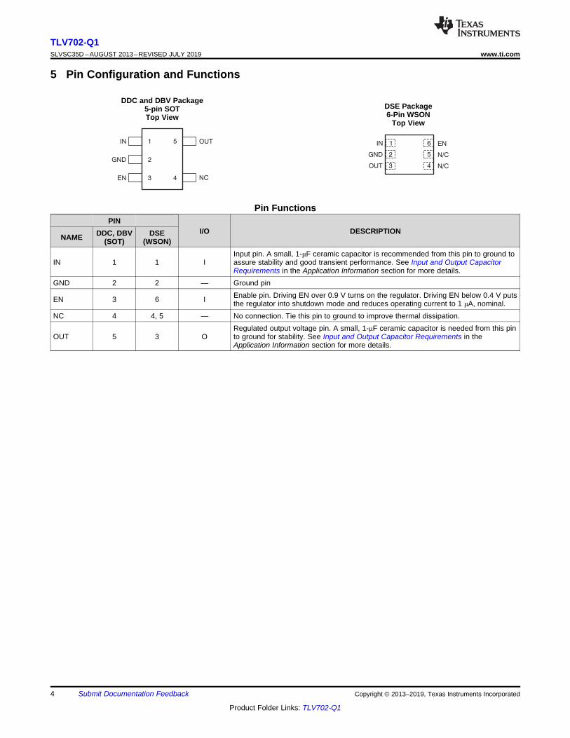
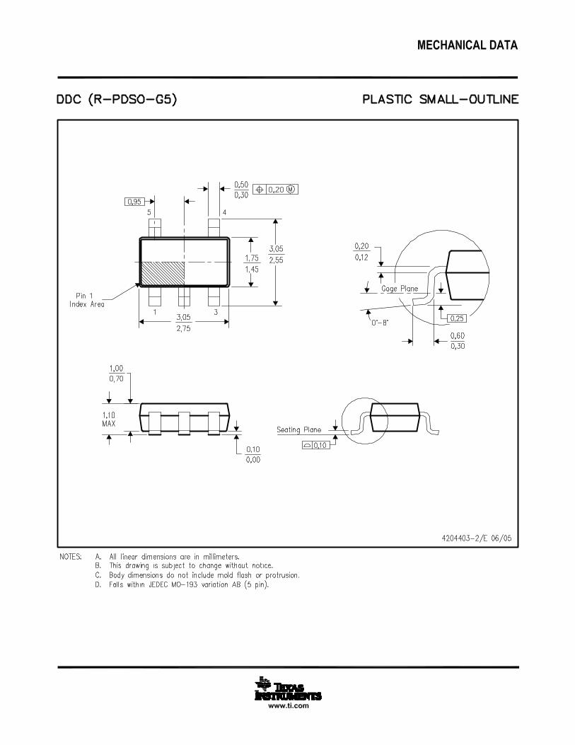
5 Pin Configuration and Functions
DDC and DBV Package5-pin SOTTop View
DSE Package6-Pin WSON
Top View
Pin FunctionsPIN
I/O DESCRIPTIONNAME DDC, DBV
(SOT)DSE
(WSON)
IN 1 1 IInput pin. A small, 1-μF ceramic capacitor is recommended from this pin to ground toassure stability and good transient performance. See Input and Output CapacitorRequirements in the Application Information section for more details.
GND 2 2 — Ground pin
EN 3 6 I Enable pin. Driving EN over 0.9 V turns on the regulator. Driving EN below 0.4 V putsthe regulator into shutdown mode and reduces operating current to 1 μA, nominal.
NC 4 4, 5 — No connection. Tie this pin to ground to improve thermal dissipation.
OUT 5 3 ORegulated output voltage pin. A small, 1-μF ceramic capacitor is needed from this pinto ground for stability. See Input and Output Capacitor Requirements in theApplication Information section for more details.
5
TLV702-Q1www.ti.com SLVSC35D –AUGUST 2013–REVISED JULY 2019
Product Folder Links: TLV702-Q1
Submit Documentation FeedbackCopyright © 2013–2019, Texas Instruments Incorporated
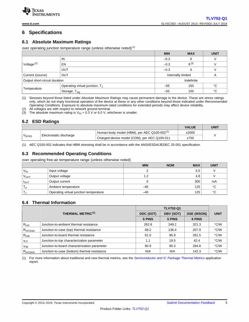
(1) Stresses beyond those listed under Absolute Maximum Ratings may cause permanent damage to the device. These are stress ratingsonly, which do not imply functional operation of the device at these or any other conditions beyond those indicated under RecommendedOperating Conditions. Exposure to absolute-maximum-rated conditions for extended periods may affect device reliability.
(2) All voltages are with respect to network ground terminal.(3) The absolute maximum rating is VIN + 0.3 V or 6.0 V, whichever is smaller.
6 Specifications
6.1 Absolute Maximum Ratingsover operating junction temperature range (unless otherwise noted) (1)
MIN MAX UNIT
Voltage (2)
IN –0.3 6 VEN –0.3 6 (3) VOUT –0.3 6 V
Current (source) OUT Internally limited AOutput short-circuit duration Indefinite
TemperatureOperating virtual junction, TJ –55 150 °CStorage, Tstg –55 150 °C
(1) AEC Q100-002 indicates that HBM stressing shall be in accordance with the ANSI/ESDA/JEDEC JS-001 specification.
6.2 ESD RatingsVALUE UNIT
V(ESD) Electrostatic dischargeHuman-body model (HBM), per AEC Q100-002 (1) ±2000
VCharged-device model (CDM), per AEC Q100-011 ±750
6.3 Recommended Operating Conditionsover operating free-air temperature range (unless otherwise noted)
MIN NOM MAX UNITVIN Input voltage 2 5.5 VVOUT Output voltage 1.2 4.8 VIOUT Output current 0 300 mATA Ambient temperature –40 125 °CTJ Operating virtual junction temperature –40 125 °C
(1) For more information about traditional and new thermal metrics, see the Semiconductor and IC Package Thermal Metrics applicationreport.
6.4 Thermal Information
THERMAL METRIC (1)TLV702-Q1
UNITDDC (SOT) DBV (SOT) DSE (WSON)5 PINS 5 PINS 6 PINS
RθJA Junction-to-ambient thermal resistance 262.8 249.2 321.3 °C/WRθJC(top) Junction-to-case (top) thermal resistance 68.2 136.4 207.9 °C/WRθJB Junction-to-board thermal resistance 81.6 85.9 281.5 °C/WψJT Junction-to-top characterization parameter 1.1 19.5 42.4 °C/WψJB Junction-to-board characterization parameter 80.9 85.3 284.8 °C/WRθJC(bot) Junction-to-case (bottom) thermal resistance N/A N/A 142.3 °C/W
6
TLV702-Q1SLVSC35D –AUGUST 2013–REVISED JULY 2019 www.ti.com
Product Folder Links: TLV702-Q1
Submit Documentation Feedback Copyright © 2013–2019, Texas Instruments Incorporated
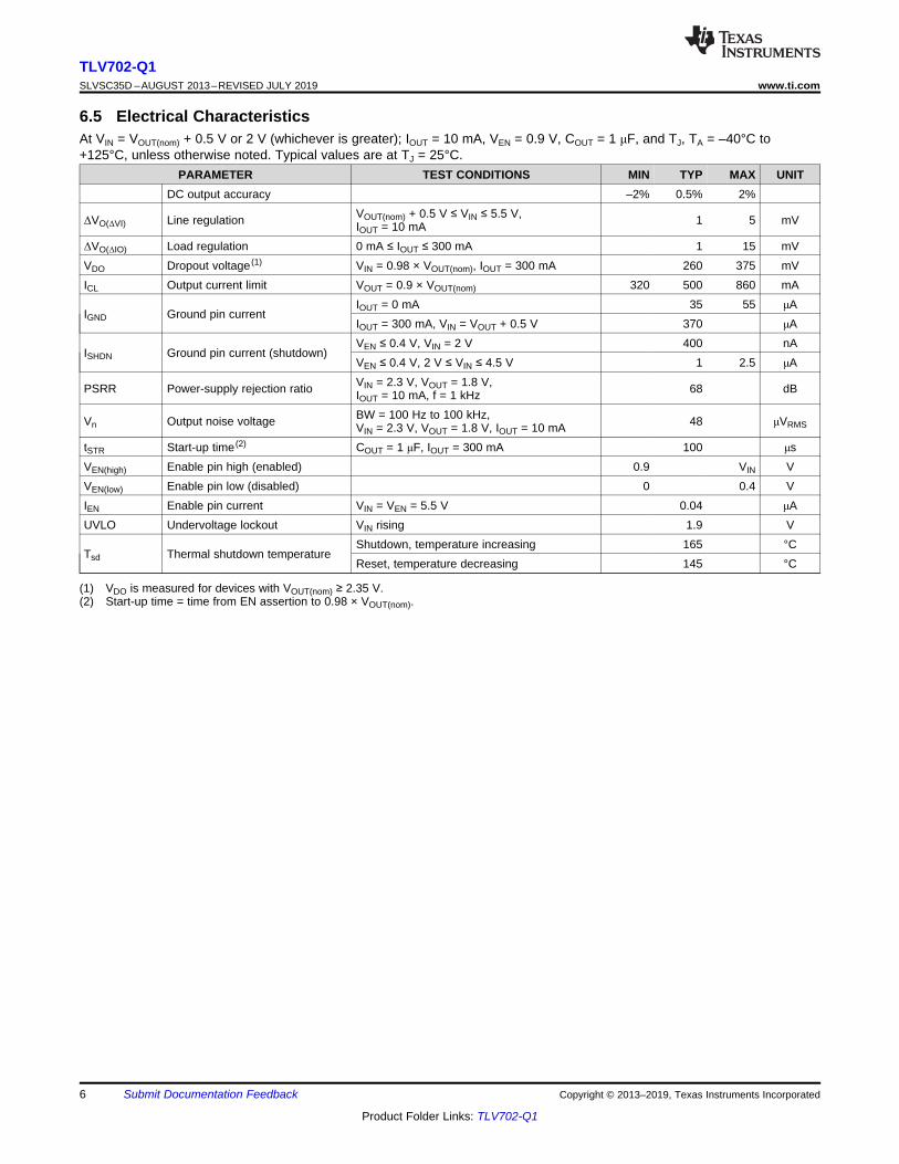
(1) VDO is measured for devices with VOUT(nom) ≥ 2.35 V.(2) Start-up time = time from EN assertion to 0.98 × VOUT(nom).
6.5 Electrical CharacteristicsAt VIN = VOUT(nom) + 0.5 V or 2 V (whichever is greater); IOUT = 10 mA, VEN = 0.9 V, COUT = 1 μF, and TJ, TA = –40°C to+125°C, unless otherwise noted. Typical values are at TJ = 25°C.
PARAMETER TEST CONDITIONS MIN TYP MAX UNITDC output accuracy –2% 0.5% 2%
ΔVO(ΔVI) Line regulation VOUT(nom) + 0.5 V ≤ VIN ≤ 5.5 V,IOUT = 10 mA 1 5 mV
ΔVO(ΔIO) Load regulation 0 mA ≤ IOUT ≤ 300 mA 1 15 mVVDO Dropout voltage (1) VIN = 0.98 × VOUT(nom), IOUT = 300 mA 260 375 mVICL Output current limit VOUT = 0.9 × VOUT(nom) 320 500 860 mA
IGND Ground pin currentIOUT = 0 mA 35 55 μAIOUT = 300 mA, VIN = VOUT + 0.5 V 370 μA
ISHDN Ground pin current (shutdown)VEN ≤ 0.4 V, VIN = 2 V 400 nAVEN ≤ 0.4 V, 2 V ≤ VIN ≤ 4.5 V 1 2.5 μA
PSRR Power-supply rejection ratio VIN = 2.3 V, VOUT = 1.8 V,IOUT = 10 mA, f = 1 kHz 68 dB
Vn Output noise voltage BW = 100 Hz to 100 kHz,VIN = 2.3 V, VOUT = 1.8 V, IOUT = 10 mA 48 μVRMS
tSTR Start-up time (2) COUT = 1 μF, IOUT = 300 mA 100 μsVEN(high) Enable pin high (enabled) 0.9 VIN VVEN(low) Enable pin low (disabled) 0 0.4 VIEN Enable pin current VIN = VEN = 5.5 V 0.04 μAUVLO Undervoltage lockout VIN rising 1.9 V
Tsd Thermal shutdown temperatureShutdown, temperature increasing 165 °CReset, temperature decreasing 145 °C
0 100 150 300
I (mA)OUT
300
250
200
150
100
50
0
V(m
V)
DO
50 200
+125 C°
+85 C°
+25 C°
-40 C°
V = 4.8 VOUT
250
1.90
1.88
1.86
1.84
1.82
1.80
1.78
1.76
1.74
1.72
1.70
V(V
)O
UT
-40 -25 -10 5 20 35 50 65 80 95 110
Temperature ( C)°
125
10mA
150mA
200mA
V = 1.8 VOUT
0 100 150 300
I (mA)OUT
1.90
1.88
1.86
1.84
1.82
1.80
1.78
1.76
1.74
1.72
1.70
V(V
)O
UT
50 200
+125 C°
+85 C°
+25 C°
-40 C°
V = 1.8 VOUT
250
350
300
250
200
150
100
50
0
V(m
V)
DO
2.25 2.75 3.25 3.75 4.25 4.75
V (V)IN
+125 C°
+85 C°
+25 C°
–40 C°
I = 300 mAOUT
1.90
1.88
1.86
1.84
1.82
1.80
1.78
1.76
1.74
1.72
1.70
VO
UT
(V)
2.1 2.6 3.1 3.6 4.1 4.6 5.1
V (V)IN
5.6
+125 C°
+85 C°
+25 C°
-40 C°
V = 1.8 V
I = 10 mAOUT
OUT
1.90
1.88
1.86
1.84
1.82
1.80
1.78
1.76
1.74
1.72
1.70
VO
UT
(V)
2.3 2.7 3.1 3.5 3.9 4.3 4.7
V (V)IN
5.55.1
+125 C°
+85 C°
+25 C°
-40 C°
V = 1.8 V
I = 300 mAOUT
OUT
7
TLV702-Q1www.ti.com SLVSC35D –AUGUST 2013–REVISED JULY 2019
Product Folder Links: TLV702-Q1
Submit Documentation FeedbackCopyright © 2013–2019, Texas Instruments Incorporated
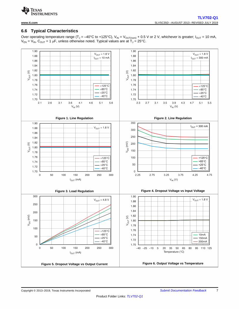
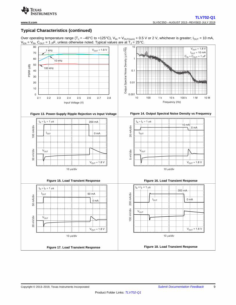
6.6 Typical CharacteristicsOver operating temperature range (TJ = –40°C to +125°C), VIN = VOUT(nom) + 0.5 V or 2 V, whichever is greater; IOUT = 10 mA,VEN = VIN, COUT = 1 μF, unless otherwise noted. Typical values are at TJ = 25°C.
Figure 1. Line Regulation Figure 2. Line Regulation
Figure 3. Load Regulation Figure 4. Dropout Voltage vs Input Voltage
Figure 5. Dropout Voltage vs Output Current Figure 6. Output Voltage vs Temperature
100
90
80
70
60
50
40
30
20
10
0
PS
RR
(d
B)
10 100 1 k 10 k 100 k 1 M 10 M
Frequency (Hz)
I = 150 mAOUT
I = 10 mAOUT
V V = 0.5 VIN OUT-
700
600
500
400
300
200
100
0
I LIM
(mA
)
2.3 2.7 3.1 3.5 3.9 4.3 4.7
V (V)IN
5.55.1
V = 1.8 VOUT
+125 C°
+85 C°
+25 C°
-40 C°
50
45
40
35
30
25
20
15
10
5
0
I(
A)
mG
ND
-40 -25 -10 5 20 35 50 65 80 95 110
Temperature ( C)°
125
V = 1.8 VOUT
2.5
2
1.5
1
0.5
0
I SH
DN
(A
m)
2.1 2.6 3.1 3.6 4.1 4.6 5.1
V (V)IN
5.6
+125 C°
+85 C°
+25 C°
-40 C°
V = 1.8 VOUT
50
45
40
35
30
25
20
15
10
5
0
I GN
D(
Am
)
2.1 2.6 3.1 3.6 4.1 4.6 5.1
V (V)IN
5.6
+125 C°
+85 C°
+25 C°
-40 C°
V = 1.8 VOUT
450
400
350
300
250
200
150
100
50
0
I GN
D(m
A)
0
I (mA)OUT
300
+125 C°
+85 C°
+25 C°
-40 C°
V = 1.8 VOUT
50 150 250100 200
8
TLV702-Q1SLVSC35D –AUGUST 2013–REVISED JULY 2019 www.ti.com
Product Folder Links: TLV702-Q1
Submit Documentation Feedback Copyright © 2013–2019, Texas Instruments Incorporated
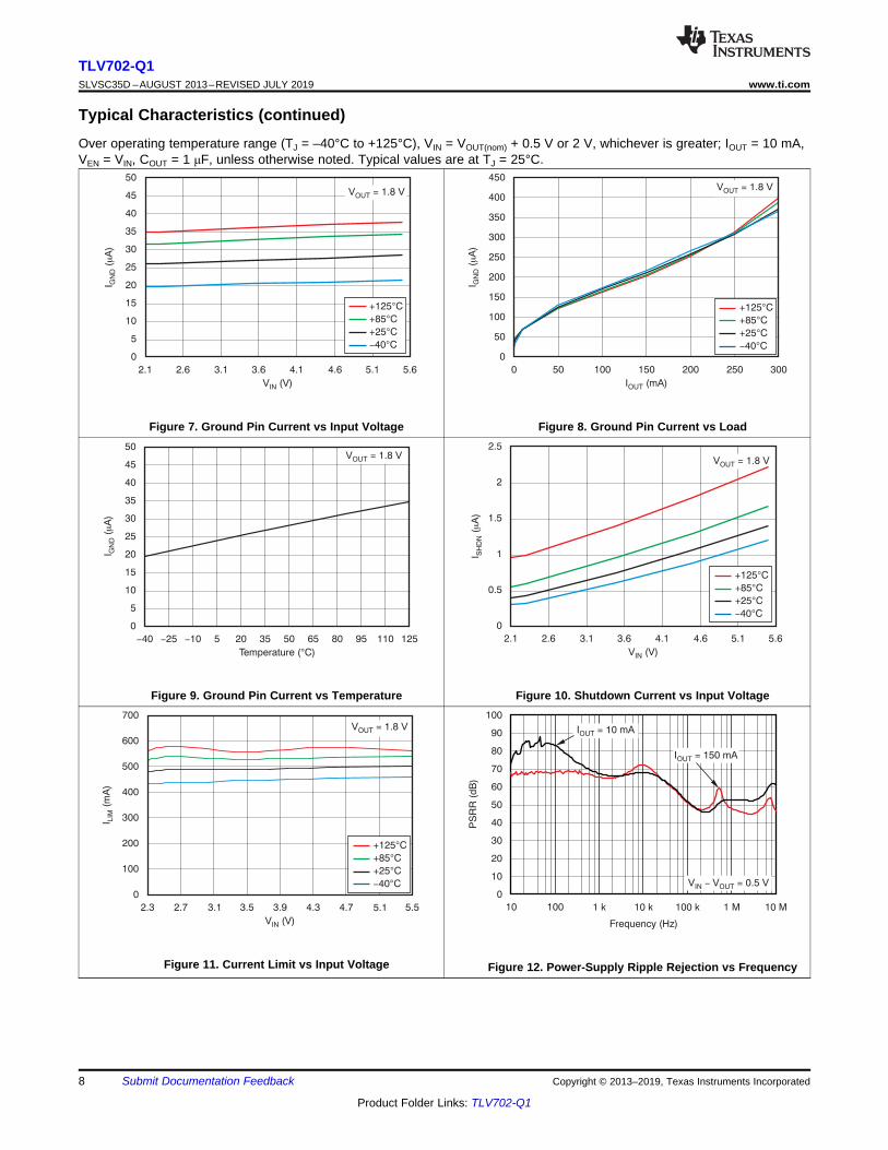
Typical Characteristics (continued)Over operating temperature range (TJ = –40°C to +125°C), VIN = VOUT(nom) + 0.5 V or 2 V, whichever is greater; IOUT = 10 mA,VEN = VIN, COUT = 1 μF, unless otherwise noted. Typical values are at TJ = 25°C.
Figure 7. Ground Pin Current vs Input Voltage Figure 8. Ground Pin Current vs Load
Figure 9. Ground Pin Current vs Temperature Figure 10. Shutdown Current vs Input Voltage
Figure 11. Current Limit vs Input Voltage Figure 12. Power-Supply Ripple Rejection vs Frequency
50
mA
/div
20
mV
/div
10 s/divm
VOUT
IOUT 50 mA
0 mA
t = t = 1 sR F m
VOUT = 1.8 V
200 m
A/d
iv100 m
V/d
iv
10 s/divm
VOUT
300 mA
0 mA
t = t = sR F
m1
IOUT
VOUT
= 1.8 V
10
0 m
A/d
iv5
0 m
V/d
iv
10 s/divm
VOUT
IOUT
200 mA
0 mA
t = t = 1 sR F m
VOUT = 1.8 V
20
mA
/div
5 m
V/d
iv
10 s/divm
VOUT
VOUT = 1.8 V
IOUT
10 mA
0 mA
t = t = 1 sR F m
2.1 2.2 2.3 2.4 2.5 2.6 2.7 2.8
Input Voltage (V)
80
70
60
50
40
30
20
10
0
PS
RR
(d
B)
10 kHz
100 kHz
1 kHz V = 1.8 VOUT
10
1
0.1
0.01
0.001
Ou
tpu
t S
pe
ctr
al N
ois
e D
en
sity (
V/
)m
ÖH
z
10 100 1 k 10 k 100 k 1 M 10 M
Frequency (Hz)
V = 1.8 VOUT
I = 10 mA
C = C = 1 FOUT
IN OUT m
9
TLV702-Q1www.ti.com SLVSC35D –AUGUST 2013–REVISED JULY 2019
Product Folder Links: TLV702-Q1
Submit Documentation FeedbackCopyright © 2013–2019, Texas Instruments Incorporated
Typical Characteristics (continued)Over operating temperature range (TJ = –40°C to +125°C), VIN = VOUT(nom) + 0.5 V or 2 V, whichever is greater; IOUT = 10 mA,VEN = VIN, COUT = 1 μF, unless otherwise noted. Typical values are at TJ = 25°C.
Figure 13. Power-Supply Ripple Rejection vs Input Voltage Figure 14. Output Spectral Noise Density vs Frequency
Figure 15. Load Transient Response Figure 16. Load Transient Response
Figure 17. Load Transient Response Figure 18. Load Transient Response
1 V
/div
10
mV
/div
1 ms/div
Slew Rate = 1 V/ sm
V = 1.8 V
I = 300 mA
OUT
OUT5.5 V
VIN2.1 V
VOUT
1 V
/div
200 ms/div
VOUT
VIN
V = 1.8 VOUT
I 1 mAOUT =
1 V
/div
5 m
V/d
iv
1 ms/div
VOUT
Slew Rate = 1 V/ sm
VIN
2.9 V
2.3 V
V = 1.8 V
I 300 mA
OUT
OUT =
1 V
/div
5 m
V/d
iv
1 ms/div
VOUT
VIN 2.9 V
2.3 V
V = 1.8 V
I 1 mA
OUT
OUT =
Slew Rate = 1 V/ sm
10
TLV702-Q1SLVSC35D –AUGUST 2013–REVISED JULY 2019 www.ti.com
Product Folder Links: TLV702-Q1
Submit Documentation Feedback Copyright © 2013–2019, Texas Instruments Incorporated
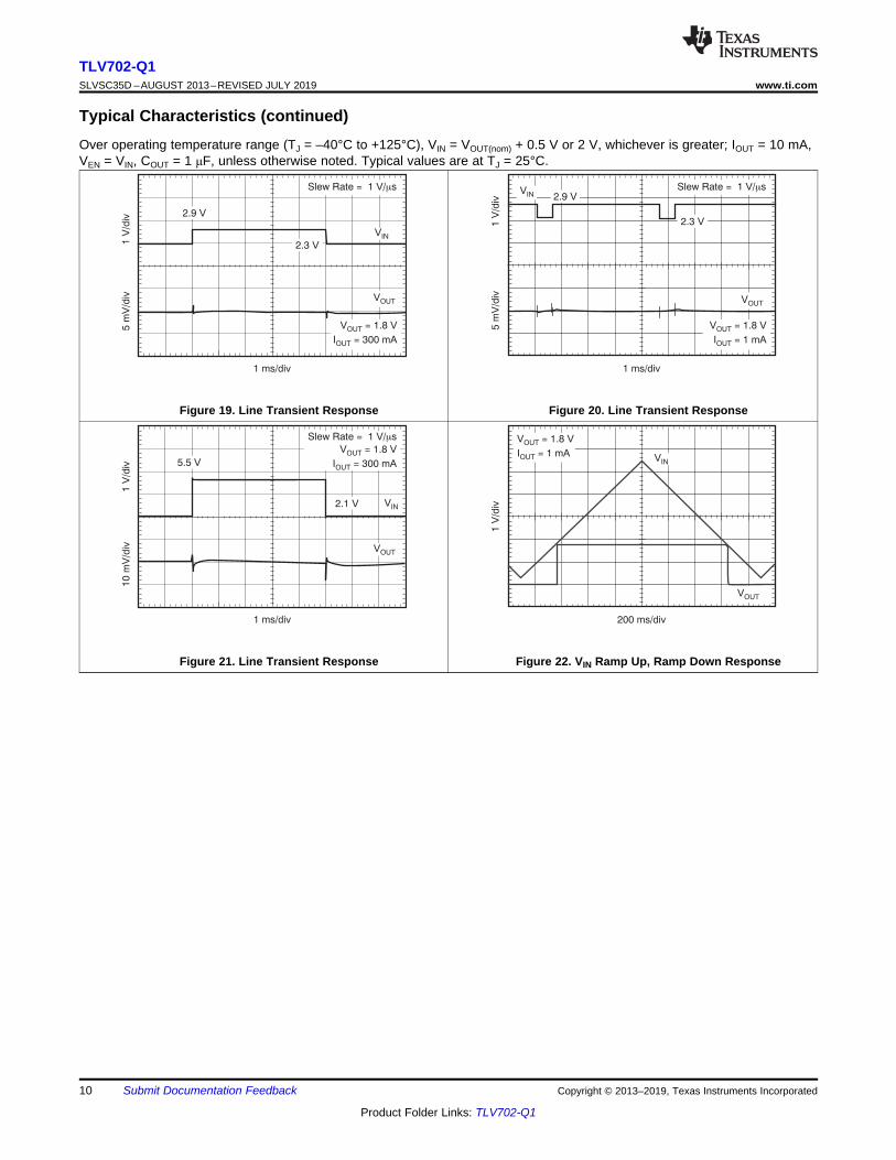
Typical Characteristics (continued)Over operating temperature range (TJ = –40°C to +125°C), VIN = VOUT(nom) + 0.5 V or 2 V, whichever is greater; IOUT = 10 mA,VEN = VIN, COUT = 1 μF, unless otherwise noted. Typical values are at TJ = 25°C.
Figure 19. Line Transient Response Figure 20. Line Transient Response
Figure 21. Line Transient Response Figure 22. VIN Ramp Up, Ramp Down Response
ThermalShutdown
CurrentLimit
UVLO
Bandgap
IN
EN
OUT
LOGIC
GND
TLV702-Q1 Series
11
TLV702-Q1www.ti.com SLVSC35D –AUGUST 2013–REVISED JULY 2019
Product Folder Links: TLV702-Q1
Submit Documentation FeedbackCopyright © 2013–2019, Texas Instruments Incorporated
7 Detailed Description
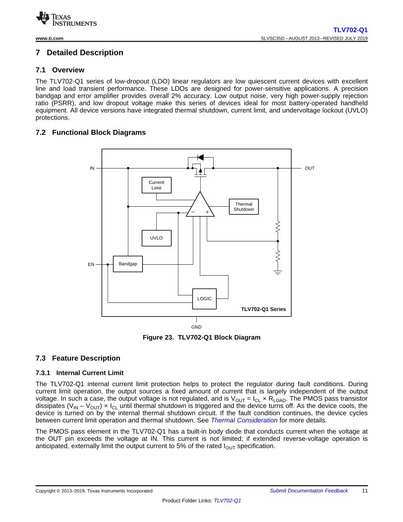
7.1 OverviewThe TLV702-Q1 series of low-dropout (LDO) linear regulators are low quiescent current devices with excellentline and load transient performance. These LDOs are designed for power-sensitive applications. A precisionbandgap and error amplifier provides overall 2% accuracy. Low output noise, very high power-supply rejectionratio (PSRR), and low dropout voltage make this series of devices ideal for most battery-operated handheldequipment. All device versions have integrated thermal shutdown, current limit, and undervoltage lockout (UVLO)protections.
7.2 Functional Block Diagrams
Figure 23. TLV702-Q1 Block Diagram
7.3 Feature Description
7.3.1 Internal Current LimitThe TLV702-Q1 internal current limit protection helps to protect the regulator during fault conditions. Duringcurrent limit operation, the output sources a fixed amount of current that is largely independent of the outputvoltage. In such a case, the output voltage is not regulated, and is VOUT = ICL × RLOAD. The PMOS pass transistordissipates (VIN – VOUT) × ICL until thermal shutdown is triggered and the device turns off. As the device cools, thedevice is turned on by the internal thermal shutdown circuit. If the fault condition continues, the device cyclesbetween current limit operation and thermal shutdown. See Thermal Consideration for more details.
The PMOS pass element in the TLV702-Q1 has a built-in body diode that conducts current when the voltage atthe OUT pin exceeds the voltage at IN. This current is not limited; if extended reverse-voltage operation isanticipated, externally limit the output current to 5% of the rated IOUT specification.
12
TLV702-Q1SLVSC35D –AUGUST 2013–REVISED JULY 2019 www.ti.com
Product Folder Links: TLV702-Q1
Submit Documentation Feedback Copyright © 2013–2019, Texas Instruments Incorporated
Feature Description (continued)7.3.2 ShutdownThe enable pin (EN) is active high. The device is enabled when voltage at EN pin exceeds 0.9 V. The device isturned off when the EN pin is held at less than 0.4 V. When shutdown capability is not required, connect the ENpin to the IN pin.
7.3.3 Dropout VoltageThe TLV702-Q1 uses a PMOS pass transistor to achieve low dropout. When (VIN – VOUT) is less than thedropout voltage (VDO), the PMOS pass device is in the linear (triode) region of operation. The input-to-outputresistance is equal to the drain-source on-state resistance (RDS(on)) of the PMOS pass element. VDO scalesapproximately with output current because the PMOS device behaves as a resistor in dropout.
As with any linear regulator, PSRR and transient response are degraded as (VIN – VOUT) approaches dropout.This effect is shown in Figure 13.
7.3.4 Undervoltage LockoutThe TLV702-Q1 uses a UVLO circuit to keep the output shut off until internal circuitry is operating properly.
7.4 Device Functional Modes
7.4.1 Normal OperationThe device regulates to the nominal output voltage under the following conditions:
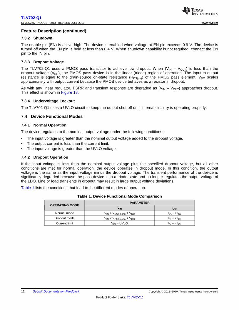
• The input voltage is greater than the nominal output voltage added to the dropout voltage.• The output current is less than the current limit.• The input voltage is greater than the UVLO voltage.
7.4.2 Dropout OperationIf the input voltage is less than the nominal output voltage plus the specified dropout voltage, but all otherconditions are met for normal operation, the device operates in dropout mode. In this condition, the outputvoltage is the same as the input voltage minus the dropout voltage. The transient performance of the device issignificantly degraded because the pass device is in a triode state and no longer regulates the output voltage ofthe LDO. Line or load transients in dropout may result in large output voltage deviations.
Table 1 lists the conditions that lead to the different modes of operation.
Table 1. Device Functional Mode Comparison
OPERATING MODEPARAMETER
VIN IOUT
Normal mode VIN > VOUT(nom) + VDO IOUT < ICL
Dropout mode VIN < VOUT(nom) + VDO IOUT < ICL
Current limit VIN > UVLO IOUT > ICL
TLV702-Q1
GNDEN
IN OUTVIN VOUT
On
Off
CIN1 �FCeramicCOUT
13
TLV702-Q1www.ti.com SLVSC35D –AUGUST 2013–REVISED JULY 2019
Product Folder Links: TLV702-Q1
Submit Documentation FeedbackCopyright © 2013–2019, Texas Instruments Incorporated
8 Application and Implementation
NOTEInformation in the following applications sections is not part of the TI componentspecification, and TI does not warrant its accuracy or completeness. TI’s customers areresponsible for determining suitability of components for their purposes. Customers shouldvalidate and test their design implementation to confirm system functionality.
8.1 Application InformationThe TLV702-Q1 belongs to a new family of next-generation value LDO regulators. These devices consume lowquiescent current and deliver excellent line and load transient performance. These characteristics, combined withlow noise and very good PSRR with little (VIN – VOUT) headroom, make this family of devices ideal for portableRF applications. This family of regulators offers current limit and thermal protection, and is specified from –40°Cto +125°C.
8.2 Typical Application
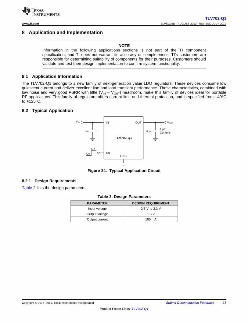
Figure 24. Typical Application Circuit
8.2.1 Design RequirementsTable 2 lists the design parameters.
Table 2. Design ParametersPARAMETER DESIGN REQUIREMENTInput voltage 2.5 V to 3.3 V
Output voltage 1.8 VOutput current 100 mA
50
mA
/div
20
mV
/div
10 s/divm
VOUT
IOUT 50 mA
0 mA
t = t = 1 sR F m
VOUT = 1.8 V
1 V
/div
5 m
V/d
iv
1 ms/div
VOUT
VIN 2.9 V
2.3 V
V = 1.8 V
I 1 mA
OUT
OUT =
Slew Rate = 1 V/ sm
14
TLV702-Q1SLVSC35D –AUGUST 2013–REVISED JULY 2019 www.ti.com
Product Folder Links: TLV702-Q1
Submit Documentation Feedback Copyright © 2013–2019, Texas Instruments Incorporated
8.2.2 Detailed Design Procedure
8.2.2.1 Input and Output Capacitor Requirements1-μF X5R- and X7R-type ceramic capacitors are recommended because these capacitors have minimal variationin value and equivalent series resistance (ESR) over temperature.
However, the TLV702-Q1 is designed to be stable with an effective capacitance of 0.1 μF or larger at the output.Thus, the device is stable with capacitors of other dielectric types as well, as long as the effective capacitanceunder operating bias voltage and temperature is greater than 0.1 μF. This effective capacitance refers to thecapacitance that the LDO sees under operating bias voltage and temperature conditions; that is, the capacitanceafter taking both bias voltage and temperature derating into consideration. In addition to allowing the use oflower-cost dielectrics, this capability of being stable with 0.1-μF effective capacitance also enables the use ofsmaller footprint capacitors that have higher derating in size- and space-constrained applications.
Using a 0.1-μF rated capacitor at the output of the LDO does not ensure stability because the effectivecapacitance under the specified operating conditions must not be less than 0.1 μF. Maximum ESR should beless than 200 mΩ.
Although an input capacitor is not required for stability, it is good analog design practice to connect a 0.1-μF to 1-μF, low ESR capacitor across the IN pin and GND pin of the regulator. This capacitor counteracts reactive inputsources and improves transient response, noise rejection, and ripple rejection. A higher-value capacitor may benecessary if large, fast rise-time load transients are anticipated, or if the device is not located close to the powersource. If source impedance is more than 2 Ω, a 0.1-μF input capacitor may be necessary for stability.
8.2.2.2 Transient ResponseAs with any regulator, increasing the size of the output capacitor reduces overshoot and undershoot magnitude,but increases the duration of the transient response.
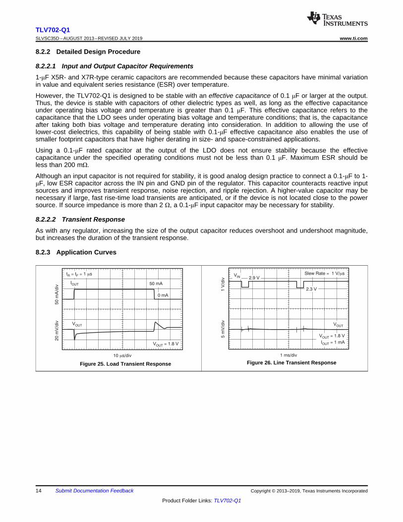
8.2.3 Application Curves
Figure 25. Load Transient Response Figure 26. Line Transient Response
P = (V V ) I- ´D IN OUT OUT
15
TLV702-Q1www.ti.com SLVSC35D –AUGUST 2013–REVISED JULY 2019
Product Folder Links: TLV702-Q1
Submit Documentation FeedbackCopyright © 2013–2019, Texas Instruments Incorporated
9 Power Supply RecommendationsConnect a low output impedance power supply directly to the IN pin of the TLV702-Q1. Inductive impedancesbetween the input supply and the IN pin can create significant voltage excursions at the IN pin during start-up orload transient events.
9.1 Power DissipationThe ability to remove heat from the die is different for each package type, presenting different considerations inthe printed-circuit-board (PCB) layout. The PCB area around the device that is free of other components movesthe heat from the device to the ambient air.
Refer to Thermal Information for thermal performance on the TLV702-Q1 evaluation module (EVM). The EVM isa two-layer board with two ounces of copper per side.
Power dissipation depends on input voltage and load conditions. Power dissipation (PD) is equal to the product ofthe output current and the voltage drop across the output pass element, as shown in Equation 1.
(1)
10 Layout
10.1 Layout GuidelinesPlace the input and output capacitors as close to the device pins as possible. To improve ac performance suchas PSRR, output noise, and transient response, design the board with separate ground planes for VIN and VOUT,with the ground plane connected only at the GND pin of the device. In addition, connect the ground connectionfor the output capacitor directly to the GND pin of the device. High-ESR capacitors may degrade PSRRperformance.
10.1.1 Thermal ConsiderationThermal protection disables the output when the junction temperature rises to approximately 165°C, allowing thedevice to cool. When the junction temperature cools to approximately 145°C, the output circuitry is againenabled. Depending on power dissipation, thermal resistance, and ambient temperature, the thermal protectioncircuit may cycle on and off. This cycling limits the dissipation of the regulator, protecting it from damage as aresult of overheating.
Any tendency to activate the thermal protection circuit indicates excessive power dissipation or an inadequateheatsink. For reliable operation, limit junction temperature to 125°C maximum.
To estimate the margin of safety in a complete design (including heatsink), increase the ambient temperatureuntil the thermal protection is triggered; use worst-case loads and signal conditions.
The internal protection circuitry of the TLV702-Q1 is designed to protect against overload conditions but is notintended to replace proper heatsinking. Continuously running the TLV702-Q1 into thermal shutdown degradesdevice reliability.
COUTVOUT
VIN
GND PLANE
CIN
Represents via used for application specific connections
IN
GND
OUT NC
EN
NC
COUT
VOUTVIN
GND PLANE
CIN
Represents via used for application specific connections
IN
GND
EN NC
OUT
16
TLV702-Q1SLVSC35D –AUGUST 2013–REVISED JULY 2019 www.ti.com
Product Folder Links: TLV702-Q1
Submit Documentation Feedback Copyright © 2013–2019, Texas Instruments Incorporated
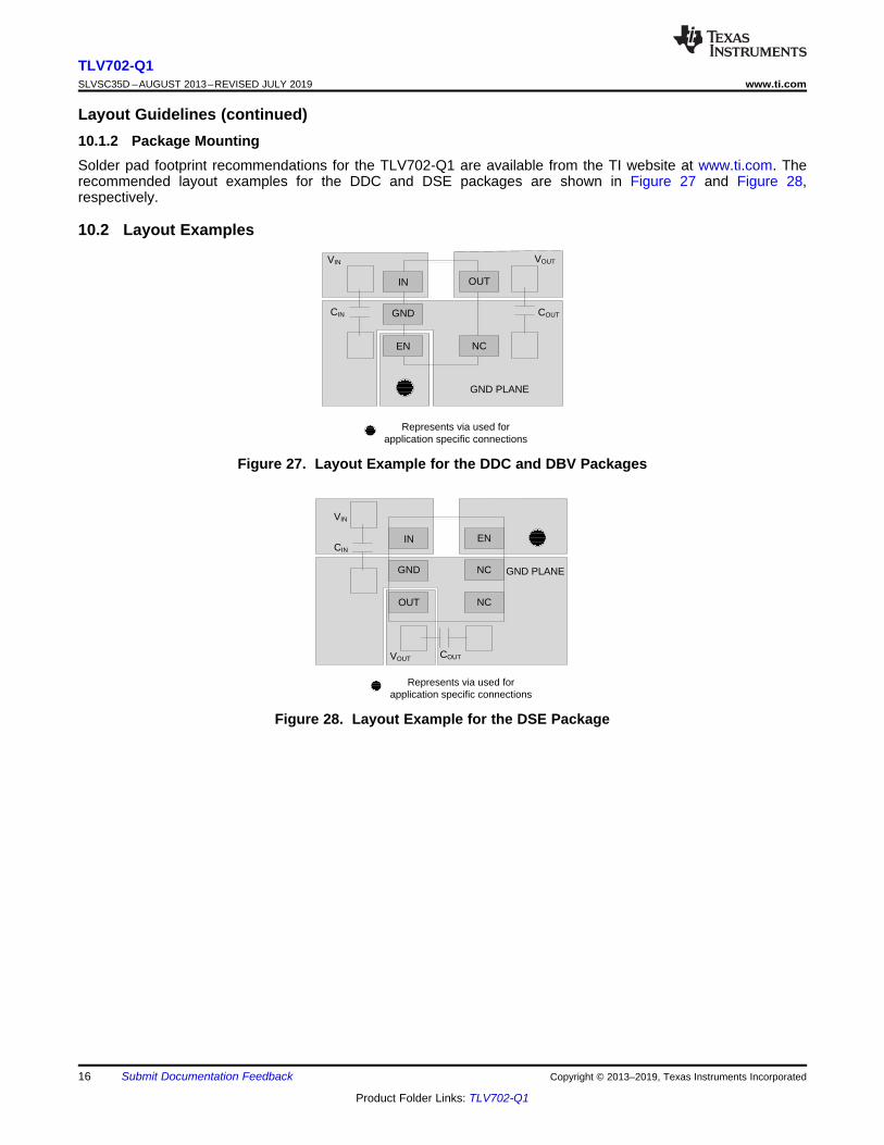
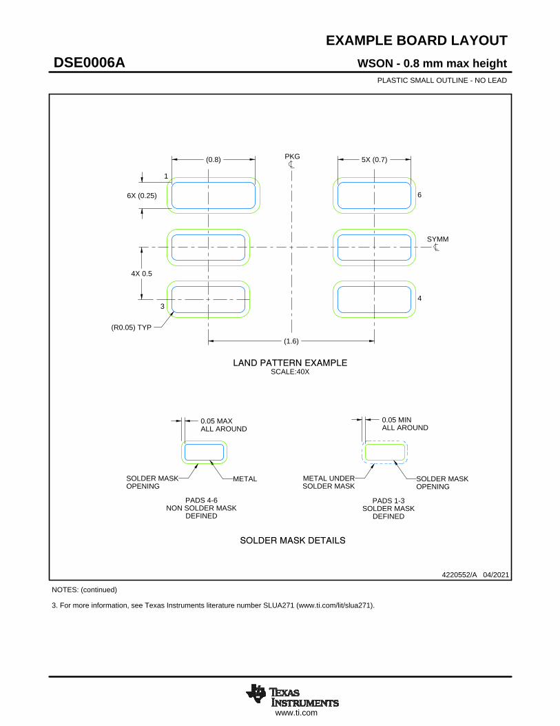
Layout Guidelines (continued)10.1.2 Package MountingSolder pad footprint recommendations for the TLV702-Q1 are available from the TI website at www.ti.com. Therecommended layout examples for the DDC and DSE packages are shown in Figure 27 and Figure 28,respectively.
10.2 Layout Examples
Figure 27. Layout Example for the DDC and DBV Packages
Figure 28. Layout Example for the DSE Package
17
TLV702-Q1www.ti.com SLVSC35D –AUGUST 2013–REVISED JULY 2019
Product Folder Links: TLV702-Q1
Submit Documentation FeedbackCopyright © 2013–2019, Texas Instruments Incorporated
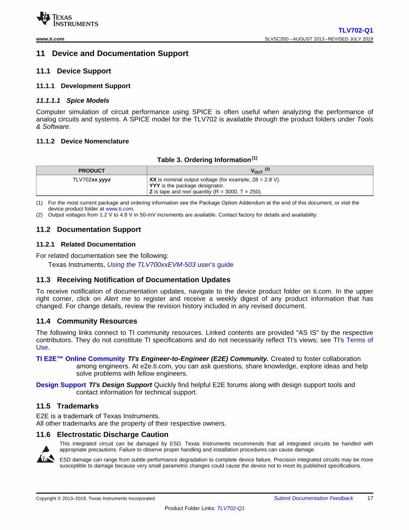
(1) For the most current package and ordering information see the Package Option Addendum at the end of this document, or visit thedevice product folder at www.ti.com.
(2) Output voltages from 1.2 V to 4.8 V in 50-mV increments are available. Contact factory for details and availability.
11 Device and Documentation Support
11.1 Device Support
11.1.1 Development Support
11.1.1.1 Spice ModelsComputer simulation of circuit performance using SPICE is often useful when analyzing the performance ofanalog circuits and systems. A SPICE model for the TLV702 is available through the product folders under Tools& Software.
11.1.2 Device Nomenclature
Table 3. Ordering Information (1)
PRODUCT VOUT(2)
TLV702xx yyyz XX is nominal output voltage (for example, 28 = 2.8 V).YYY is the package designator.Z is tape and reel quantity (R = 3000, T = 250).
11.2 Documentation Support
11.2.1 Related DocumentationFor related documentation see the following:
Texas Instruments, Using the TLV700xxEVM-503 user's guide
11.3 Receiving Notification of Documentation UpdatesTo receive notification of documentation updates, navigate to the device product folder on ti.com. In the upperright corner, click on Alert me to register and receive a weekly digest of any product information that haschanged. For change details, review the revision history included in any revised document.
11.4 Community ResourcesThe following links connect to TI community resources. Linked contents are provided "AS IS" by the respectivecontributors. They do not constitute TI specifications and do not necessarily reflect TI's views; see TI's Terms ofUse.
TI E2E™ Online Community TI's Engineer-to-Engineer (E2E) Community. Created to foster collaborationamong engineers. At e2e.ti.com, you can ask questions, share knowledge, explore ideas and helpsolve problems with fellow engineers.
Design Support TI's Design Support Quickly find helpful E2E forums along with design support tools andcontact information for technical support.
11.5 TrademarksE2E is a trademark of Texas Instruments.All other trademarks are the property of their respective owners.
11.6 Electrostatic Discharge CautionThis integrated circuit can be damaged by ESD. Texas Instruments recommends that all integrated circuits be handled withappropriate precautions. Failure to observe proper handling and installation procedures can cause damage.
ESD damage can range from subtle performance degradation to complete device failure. Precision integrated circuits may be moresusceptible to damage because very small parametric changes could cause the device not to meet its published specifications.
18
TLV702-Q1SLVSC35D –AUGUST 2013–REVISED JULY 2019 www.ti.com
Product Folder Links: TLV702-Q1
Submit Documentation Feedback Copyright © 2013–2019, Texas Instruments Incorporated
11.7 GlossarySLYZ022 — TI Glossary.
This glossary lists and explains terms, acronyms, and definitions.
12 Mechanical, Packaging, and Orderable InformationThe following pages include mechanical, packaging, and orderable information. This information is the mostcurrent data available for the designated devices. This data is subject to change without notice and revision ofthis document. For browser-based versions of this data sheet, refer to the left-hand navigation.
PACKAGE OPTION ADDENDUM
www.ti.com 10-Dec-2020
Addendum-Page 1
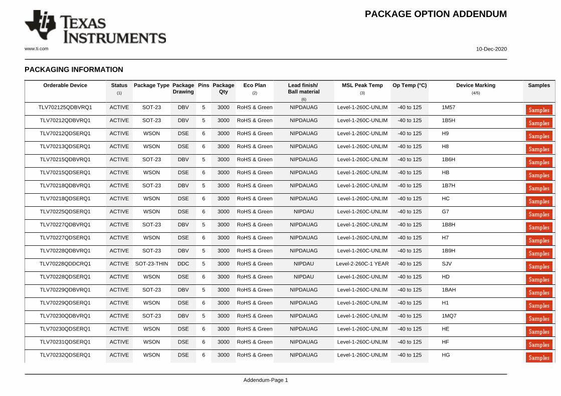
PACKAGING INFORMATION
Orderable Device Status(1)
Package Type PackageDrawing
Pins PackageQty
Eco Plan(2)
Lead finish/Ball material
(6)
MSL Peak Temp(3)
Op Temp (°C) Device Marking(4/5)
Samples
TLV702125QDBVRQ1 ACTIVE SOT-23 DBV 5 3000 RoHS & Green NIPDAUAG Level-1-260C-UNLIM -40 to 125 1M57
TLV70212QDBVRQ1 ACTIVE SOT-23 DBV 5 3000 RoHS & Green NIPDAUAG Level-1-260C-UNLIM -40 to 125 1B5H
TLV70212QDSERQ1 ACTIVE WSON DSE 6 3000 RoHS & Green NIPDAUAG Level-1-260C-UNLIM -40 to 125 H9
TLV70213QDSERQ1 ACTIVE WSON DSE 6 3000 RoHS & Green NIPDAUAG Level-1-260C-UNLIM -40 to 125 H8
TLV70215QDBVRQ1 ACTIVE SOT-23 DBV 5 3000 RoHS & Green NIPDAUAG Level-1-260C-UNLIM -40 to 125 1B6H
TLV70215QDSERQ1 ACTIVE WSON DSE 6 3000 RoHS & Green NIPDAUAG Level-1-260C-UNLIM -40 to 125 HB
TLV70218QDBVRQ1 ACTIVE SOT-23 DBV 5 3000 RoHS & Green NIPDAUAG Level-1-260C-UNLIM -40 to 125 1B7H
TLV70218QDSERQ1 ACTIVE WSON DSE 6 3000 RoHS & Green NIPDAUAG Level-1-260C-UNLIM -40 to 125 HC
TLV70225QDSERQ1 ACTIVE WSON DSE 6 3000 RoHS & Green NIPDAU Level-1-260C-UNLIM -40 to 125 G7
TLV70227QDBVRQ1 ACTIVE SOT-23 DBV 5 3000 RoHS & Green NIPDAUAG Level-1-260C-UNLIM -40 to 125 1B8H
TLV70227QDSERQ1 ACTIVE WSON DSE 6 3000 RoHS & Green NIPDAUAG Level-1-260C-UNLIM -40 to 125 H7
TLV70228QDBVRQ1 ACTIVE SOT-23 DBV 5 3000 RoHS & Green NIPDAUAG Level-1-260C-UNLIM -40 to 125 1B9H
TLV70228QDDCRQ1 ACTIVE SOT-23-THIN DDC 5 3000 RoHS & Green NIPDAU Level-2-260C-1 YEAR -40 to 125 SJV
TLV70228QDSERQ1 ACTIVE WSON DSE 6 3000 RoHS & Green NIPDAU Level-1-260C-UNLIM -40 to 125 HD
TLV70229QDBVRQ1 ACTIVE SOT-23 DBV 5 3000 RoHS & Green NIPDAUAG Level-1-260C-UNLIM -40 to 125 1BAH
TLV70229QDSERQ1 ACTIVE WSON DSE 6 3000 RoHS & Green NIPDAUAG Level-1-260C-UNLIM -40 to 125 H1
TLV70230QDBVRQ1 ACTIVE SOT-23 DBV 5 3000 RoHS & Green NIPDAUAG Level-1-260C-UNLIM -40 to 125 1MQ7
TLV70230QDSERQ1 ACTIVE WSON DSE 6 3000 RoHS & Green NIPDAUAG Level-1-260C-UNLIM -40 to 125 HE
TLV70231QDSERQ1 ACTIVE WSON DSE 6 3000 RoHS & Green NIPDAUAG Level-1-260C-UNLIM -40 to 125 HF
TLV70232QDSERQ1 ACTIVE WSON DSE 6 3000 RoHS & Green NIPDAUAG Level-1-260C-UNLIM -40 to 125 HG
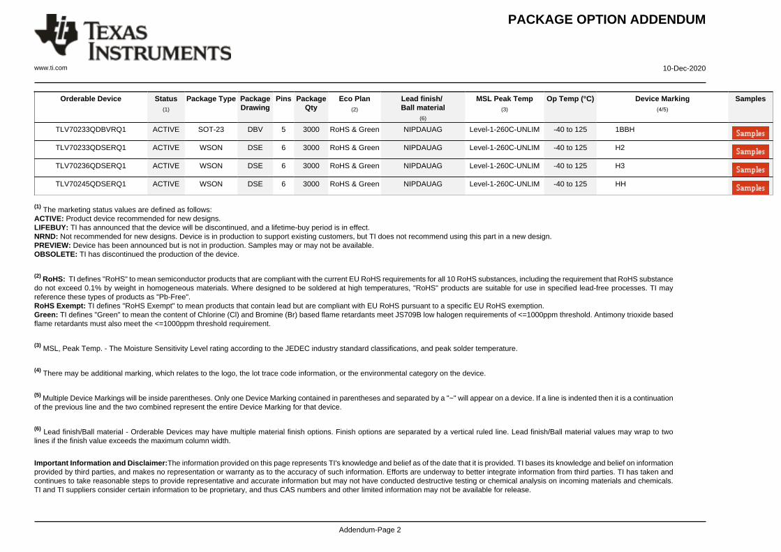
PACKAGE OPTION ADDENDUM
www.ti.com 10-Dec-2020
Addendum-Page 2
Orderable Device Status(1)
Package Type PackageDrawing
Pins PackageQty
Eco Plan(2)
Lead finish/Ball material
(6)
MSL Peak Temp(3)
Op Temp (°C) Device Marking(4/5)
Samples
TLV70233QDBVRQ1 ACTIVE SOT-23 DBV 5 3000 RoHS & Green NIPDAUAG Level-1-260C-UNLIM -40 to 125 1BBH
TLV70233QDSERQ1 ACTIVE WSON DSE 6 3000 RoHS & Green NIPDAUAG Level-1-260C-UNLIM -40 to 125 H2
TLV70236QDSERQ1 ACTIVE WSON DSE 6 3000 RoHS & Green NIPDAUAG Level-1-260C-UNLIM -40 to 125 H3
TLV70245QDSERQ1 ACTIVE WSON DSE 6 3000 RoHS & Green NIPDAUAG Level-1-260C-UNLIM -40 to 125 HH
(1) The marketing status values are defined as follows:ACTIVE: Product device recommended for new designs.LIFEBUY: TI has announced that the device will be discontinued, and a lifetime-buy period is in effect.NRND: Not recommended for new designs. Device is in production to support existing customers, but TI does not recommend using this part in a new design.PREVIEW: Device has been announced but is not in production. Samples may or may not be available.OBSOLETE: TI has discontinued the production of the device.
(2) RoHS: TI defines "RoHS" to mean semiconductor products that are compliant with the current EU RoHS requirements for all 10 RoHS substances, including the requirement that RoHS substancedo not exceed 0.1% by weight in homogeneous materials. Where designed to be soldered at high temperatures, "RoHS" products are suitable for use in specified lead-free processes. TI mayreference these types of products as "Pb-Free".RoHS Exempt: TI defines "RoHS Exempt" to mean products that contain lead but are compliant with EU RoHS pursuant to a specific EU RoHS exemption.Green: TI defines "Green" to mean the content of Chlorine (Cl) and Bromine (Br) based flame retardants meet JS709B low halogen requirements of <=1000ppm threshold. Antimony trioxide basedflame retardants must also meet the <=1000ppm threshold requirement.
(3) MSL, Peak Temp. - The Moisture Sensitivity Level rating according to the JEDEC industry standard classifications, and peak solder temperature.
(4) There may be additional marking, which relates to the logo, the lot trace code information, or the environmental category on the device.
(5) Multiple Device Markings will be inside parentheses. Only one Device Marking contained in parentheses and separated by a "~" will appear on a device. If a line is indented then it is a continuationof the previous line and the two combined represent the entire Device Marking for that device.
(6) Lead finish/Ball material - Orderable Devices may have multiple material finish options. Finish options are separated by a vertical ruled line. Lead finish/Ball material values may wrap to twolines if the finish value exceeds the maximum column width.
Important Information and Disclaimer:The information provided on this page represents TI's knowledge and belief as of the date that it is provided. TI bases its knowledge and belief on informationprovided by third parties, and makes no representation or warranty as to the accuracy of such information. Efforts are underway to better integrate information from third parties. TI has taken andcontinues to take reasonable steps to provide representative and accurate information but may not have conducted destructive testing or chemical analysis on incoming materials and chemicals.TI and TI suppliers consider certain information to be proprietary, and thus CAS numbers and other limited information may not be available for release.
PACKAGE OPTION ADDENDUM
www.ti.com 10-Dec-2020
Addendum-Page 3
In no event shall TI's liability arising out of such information exceed the total purchase price of the TI part(s) at issue in this document sold by TI to Customer on an annual basis.
OTHER QUALIFIED VERSIONS OF TLV702-Q1 :
• Catalog: TLV702
NOTE: Qualified Version Definitions:
• Catalog - TI's standard catalog product
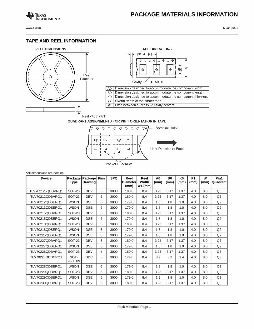
TAPE AND REEL INFORMATION
*All dimensions are nominal
Device PackageType
PackageDrawing
Pins SPQ ReelDiameter
(mm)
ReelWidth
W1 (mm)
A0(mm)
B0(mm)
K0(mm)
P1(mm)
W(mm)
Pin1Quadrant
TLV702125QDBVRQ1 SOT-23 DBV 5 3000 180.0 8.4 3.23 3.17 1.37 4.0 8.0 Q3
TLV70212QDBVRQ1 SOT-23 DBV 5 3000 180.0 8.4 3.23 3.17 1.37 4.0 8.0 Q3
TLV70212QDSERQ1 WSON DSE 6 3000 179.0 8.4 1.8 1.8 1.0 4.0 8.0 Q2
TLV70213QDSERQ1 WSON DSE 6 3000 179.0 8.4 1.8 1.8 1.0 4.0 8.0 Q2
TLV70215QDBVRQ1 SOT-23 DBV 5 3000 180.0 8.4 3.23 3.17 1.37 4.0 8.0 Q3
TLV70215QDSERQ1 WSON DSE 6 3000 179.0 8.4 1.8 1.8 1.0 4.0 8.0 Q2
TLV70218QDBVRQ1 SOT-23 DBV 5 3000 180.0 8.4 3.23 3.17 1.37 4.0 8.0 Q3
TLV70218QDSERQ1 WSON DSE 6 3000 179.0 8.4 1.8 1.8 1.0 4.0 8.0 Q2
TLV70225QDSERQ1 WSON DSE 6 3000 179.0 8.4 1.8 1.8 1.0 4.0 8.0 Q2
TLV70227QDBVRQ1 SOT-23 DBV 5 3000 180.0 8.4 3.23 3.17 1.37 4.0 8.0 Q3
TLV70227QDSERQ1 WSON DSE 6 3000 179.0 8.4 1.8 1.8 1.0 4.0 8.0 Q2
TLV70228QDBVRQ1 SOT-23 DBV 5 3000 180.0 8.4 3.23 3.17 1.37 4.0 8.0 Q3
TLV70228QDDCRQ1 SOT-23-THIN
DDC 5 3000 179.0 8.4 3.2 3.2 1.4 4.0 8.0 Q3
TLV70228QDSERQ1 WSON DSE 6 3000 179.0 8.4 1.8 1.8 1.0 4.0 8.0 Q2
TLV70229QDBVRQ1 SOT-23 DBV 5 3000 180.0 8.4 3.23 3.17 1.37 4.0 8.0 Q3
TLV70229QDSERQ1 WSON DSE 6 3000 179.0 8.4 1.8 1.8 1.0 4.0 8.0 Q2
TLV70230QDBVRQ1 SOT-23 DBV 5 3000 180.0 8.4 3.23 3.17 1.37 4.0 8.0 Q3
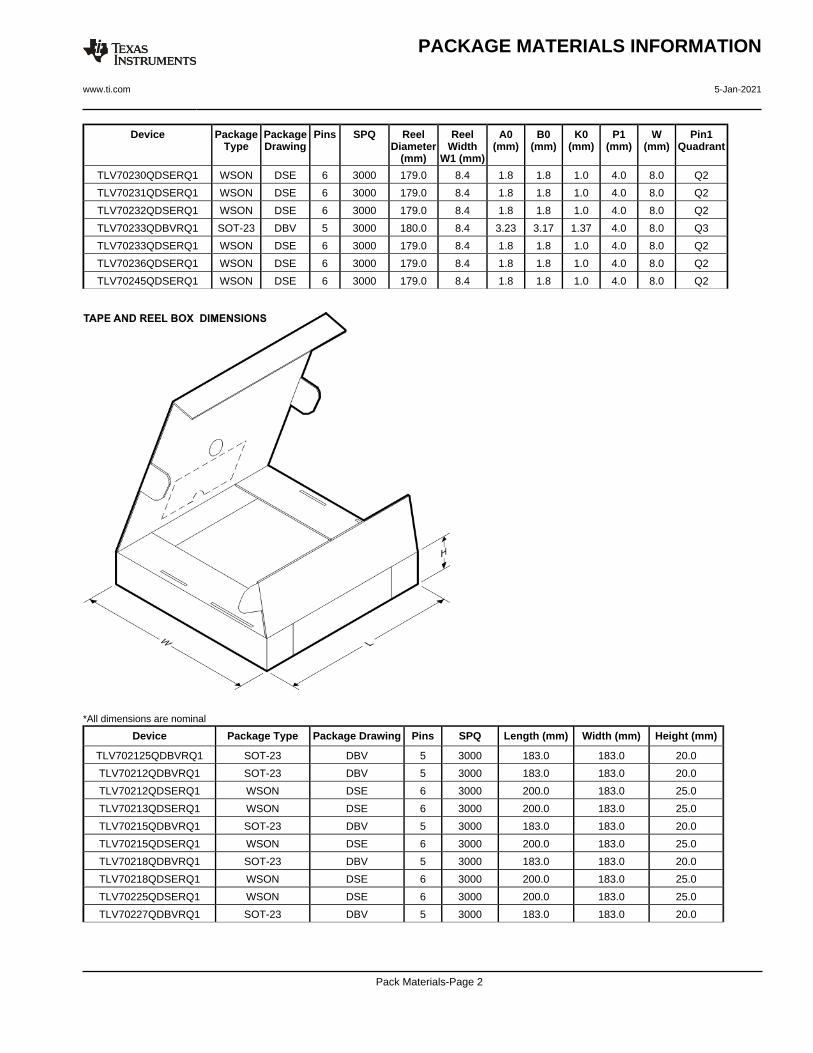
PACKAGE MATERIALS INFORMATION
www.ti.com 5-Jan-2021
Pack Materials-Page 1
Device PackageType
PackageDrawing
Pins SPQ ReelDiameter
(mm)
ReelWidth
W1 (mm)
A0(mm)
B0(mm)
K0(mm)
P1(mm)
W(mm)
Pin1Quadrant
TLV70230QDSERQ1 WSON DSE 6 3000 179.0 8.4 1.8 1.8 1.0 4.0 8.0 Q2
TLV70231QDSERQ1 WSON DSE 6 3000 179.0 8.4 1.8 1.8 1.0 4.0 8.0 Q2
TLV70232QDSERQ1 WSON DSE 6 3000 179.0 8.4 1.8 1.8 1.0 4.0 8.0 Q2
TLV70233QDBVRQ1 SOT-23 DBV 5 3000 180.0 8.4 3.23 3.17 1.37 4.0 8.0 Q3
TLV70233QDSERQ1 WSON DSE 6 3000 179.0 8.4 1.8 1.8 1.0 4.0 8.0 Q2
TLV70236QDSERQ1 WSON DSE 6 3000 179.0 8.4 1.8 1.8 1.0 4.0 8.0 Q2
TLV70245QDSERQ1 WSON DSE 6 3000 179.0 8.4 1.8 1.8 1.0 4.0 8.0 Q2
*All dimensions are nominal
Device Package Type Package Drawing Pins SPQ Length (mm) Width (mm) Height (mm)
TLV702125QDBVRQ1 SOT-23 DBV 5 3000 183.0 183.0 20.0
TLV70212QDBVRQ1 SOT-23 DBV 5 3000 183.0 183.0 20.0
TLV70212QDSERQ1 WSON DSE 6 3000 200.0 183.0 25.0
TLV70213QDSERQ1 WSON DSE 6 3000 200.0 183.0 25.0
TLV70215QDBVRQ1 SOT-23 DBV 5 3000 183.0 183.0 20.0
TLV70215QDSERQ1 WSON DSE 6 3000 200.0 183.0 25.0
TLV70218QDBVRQ1 SOT-23 DBV 5 3000 183.0 183.0 20.0
TLV70218QDSERQ1 WSON DSE 6 3000 200.0 183.0 25.0
TLV70225QDSERQ1 WSON DSE 6 3000 200.0 183.0 25.0
TLV70227QDBVRQ1 SOT-23 DBV 5 3000 183.0 183.0 20.0
PACKAGE MATERIALS INFORMATION
www.ti.com 5-Jan-2021
Pack Materials-Page 2
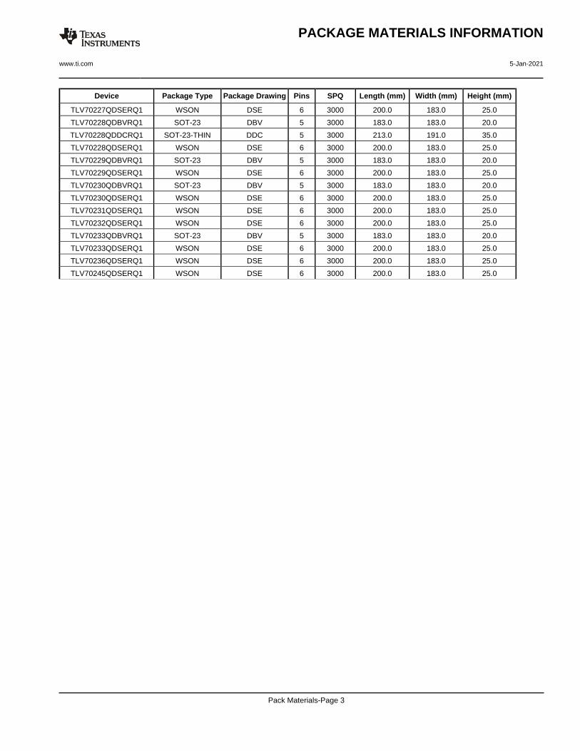
Device Package Type Package Drawing Pins SPQ Length (mm) Width (mm) Height (mm)
TLV70227QDSERQ1 WSON DSE 6 3000 200.0 183.0 25.0
TLV70228QDBVRQ1 SOT-23 DBV 5 3000 183.0 183.0 20.0
TLV70228QDDCRQ1 SOT-23-THIN DDC 5 3000 213.0 191.0 35.0
TLV70228QDSERQ1 WSON DSE 6 3000 200.0 183.0 25.0
TLV70229QDBVRQ1 SOT-23 DBV 5 3000 183.0 183.0 20.0
TLV70229QDSERQ1 WSON DSE 6 3000 200.0 183.0 25.0
TLV70230QDBVRQ1 SOT-23 DBV 5 3000 183.0 183.0 20.0
TLV70230QDSERQ1 WSON DSE 6 3000 200.0 183.0 25.0
TLV70231QDSERQ1 WSON DSE 6 3000 200.0 183.0 25.0
TLV70232QDSERQ1 WSON DSE 6 3000 200.0 183.0 25.0
TLV70233QDBVRQ1 SOT-23 DBV 5 3000 183.0 183.0 20.0
TLV70233QDSERQ1 WSON DSE 6 3000 200.0 183.0 25.0
TLV70236QDSERQ1 WSON DSE 6 3000 200.0 183.0 25.0
TLV70245QDSERQ1 WSON DSE 6 3000 200.0 183.0 25.0
PACKAGE MATERIALS INFORMATION
www.ti.com 5-Jan-2021
Pack Materials-Page 3
www.ti.com
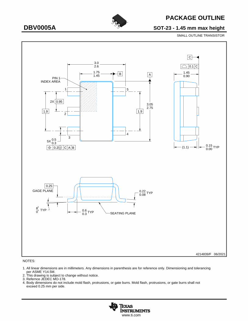
PACKAGE OUTLINE
C
0.220.08 TYP
0.25
3.02.6
2X 0.95
1.9
1.450.90
0.150.00 TYP
5X 0.50.3
0.60.3 TYP
80 TYP
1.9
A
3.052.75
B1.751.45
(1.1)
SOT-23 - 1.45 mm max heightDBV0005ASMALL OUTLINE TRANSISTOR
4214839/F 06/2021
NOTES: 1. All linear dimensions are in millimeters. Any dimensions in parenthesis are for reference only. Dimensioning and tolerancing per ASME Y14.5M.2. This drawing is subject to change without notice.3. Refernce JEDEC MO-178.4. Body dimensions do not include mold flash, protrusions, or gate burrs. Mold flash, protrusions, or gate burrs shall not exceed 0.25 mm per side.
0.2 C A B
1
34
5
2
INDEX AREAPIN 1
GAGE PLANE
SEATING PLANE
0.1 C
SCALE 4.000
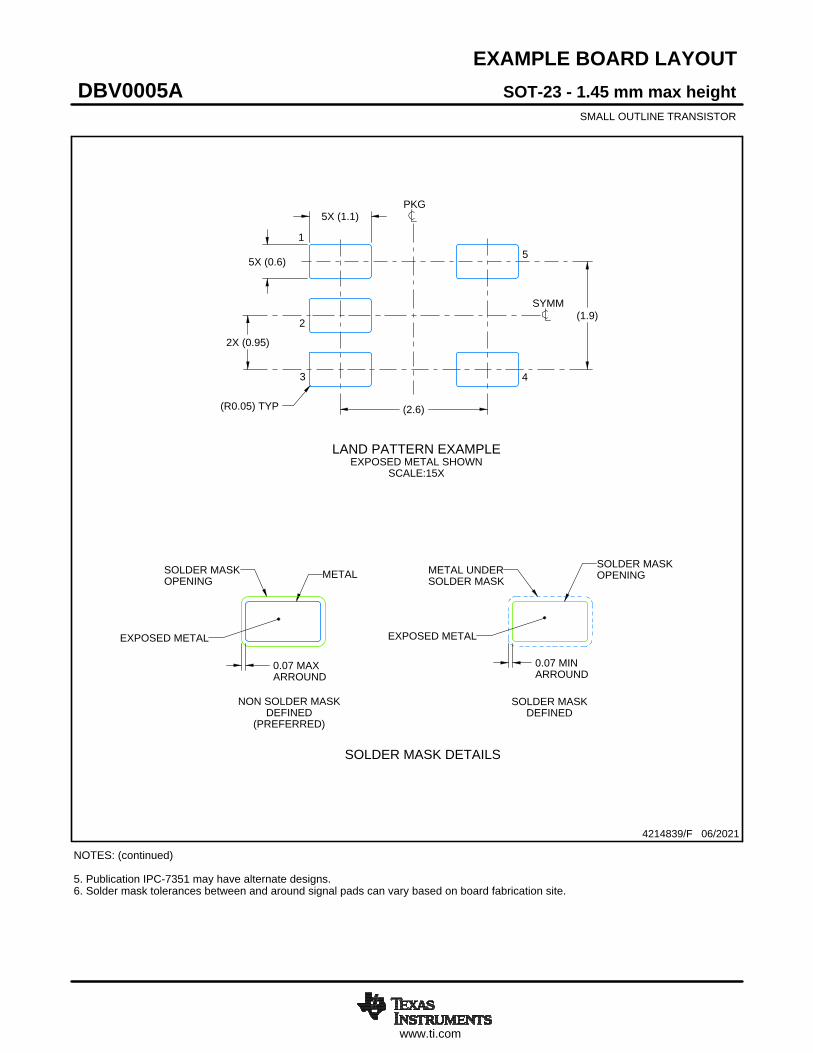
www.ti.com
EXAMPLE BOARD LAYOUT
0.07 MAXARROUND
0.07 MINARROUND
5X (1.1)
5X (0.6)
(2.6)
(1.9)
2X (0.95)
(R0.05) TYP
4214839/F 06/2021
SOT-23 - 1.45 mm max heightDBV0005ASMALL OUTLINE TRANSISTOR
NOTES: (continued) 5. Publication IPC-7351 may have alternate designs. 6. Solder mask tolerances between and around signal pads can vary based on board fabrication site.
SYMM
LAND PATTERN EXAMPLEEXPOSED METAL SHOWN
SCALE:15X
PKG
1
3 4
5
2
SOLDER MASKOPENINGMETAL UNDER
SOLDER MASK
SOLDER MASKDEFINED
EXPOSED METAL
METALSOLDER MASKOPENING
NON SOLDER MASKDEFINED
(PREFERRED)
SOLDER MASK DETAILS
EXPOSED METAL
www.ti.com
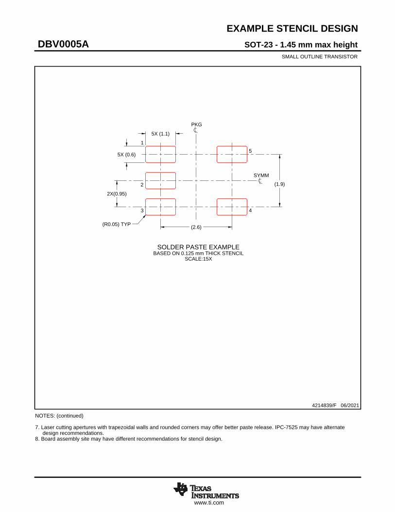
EXAMPLE STENCIL DESIGN
(2.6)
(1.9)
2X(0.95)
5X (1.1)
5X (0.6)
(R0.05) TYP
SOT-23 - 1.45 mm max heightDBV0005ASMALL OUTLINE TRANSISTOR
4214839/F 06/2021
NOTES: (continued) 7. Laser cutting apertures with trapezoidal walls and rounded corners may offer better paste release. IPC-7525 may have alternate design recommendations. 8. Board assembly site may have different recommendations for stencil design.
SOLDER PASTE EXAMPLEBASED ON 0.125 mm THICK STENCIL
SCALE:15X
SYMM
PKG
1
3 4
5
2
www.ti.com
PACKAGE OUTLINE
C
0.050.005X 0.6
0.4
(0.2) TYP
0.8 MAX
6X 0.30.20.7
0.5
2X 1
4X 0.5
B 1.551.45
A
1.551.45
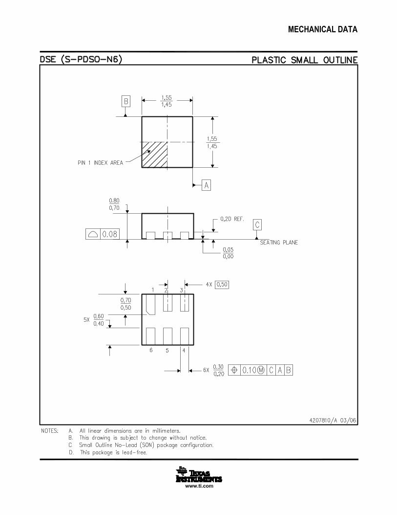
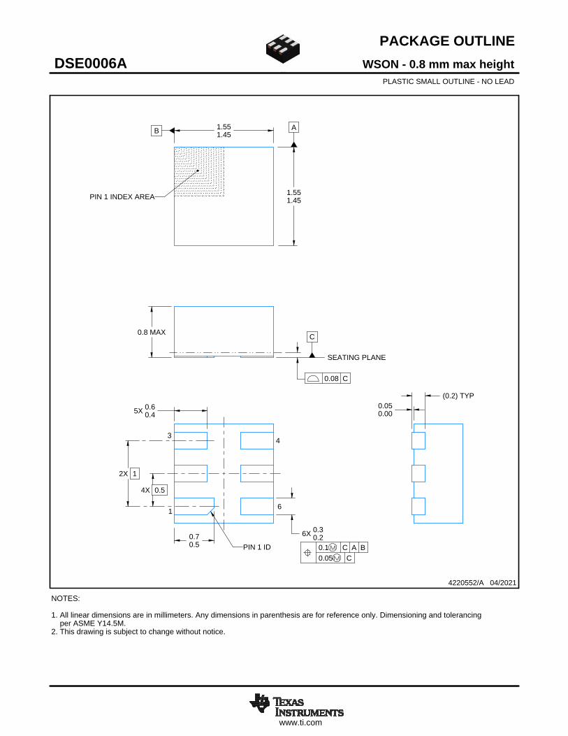
WSON - 0.8 mm max heightDSE0006APLASTIC SMALL OUTLINE - NO LEAD
4220552/A 04/2021
PIN 1 INDEX AREA
SEATING PLANE
0.08 C
1
34
6
0.1 C A B0.05 C
PIN 1 ID
NOTES: 1. All linear dimensions are in millimeters. Any dimensions in parenthesis are for reference only. Dimensioning and tolerancing per ASME Y14.5M. 2. This drawing is subject to change without notice.
SCALE 6.000
www.ti.com
EXAMPLE BOARD LAYOUT
(0.8)
4X 0.5
(1.6)
0.05 MINALL AROUND
0.05 MAXALL AROUND
6X (0.25)
(R0.05) TYP
5X (0.7)
WSON - 0.8 mm max heightDSE0006APLASTIC SMALL OUTLINE - NO LEAD
4220552/A 04/2021
PKG
1
34
6
SYMM
LAND PATTERN EXAMPLESCALE:40X
NOTES: (continued) 3. For more information, see Texas Instruments literature number SLUA271 (www.ti.com/lit/slua271).
SOLDER MASKOPENINGSOLDER MASK
METAL UNDER
PADS 1-3SOLDER MASK
DEFINED
METALSOLDER MASKOPENING
SOLDER MASK DETAILS
PADS 4-6NON SOLDER MASK
DEFINED
www.ti.com
EXAMPLE STENCIL DESIGN
(0.8) 5X (0.7)
4X (0.5)
(1.6)
6X (0.25)
(R0.05) TYP
WSON - 0.8 mm max heightDSE0006APLASTIC SMALL OUTLINE - NO LEAD
NOTES: (continued) 4. Laser cutting apertures with trapezoidal walls and rounded corners may offer better paste release. IPC-7525 may have alternate design recommendations.
SOLDER PASTE EXAMPLEBASED ON 0.125 mm THICK STENCIL
SCALE:40X
PKG
1
3 4
6
SYMM
IMPORTANT NOTICE AND DISCLAIMERTI PROVIDES TECHNICAL AND RELIABILITY DATA (INCLUDING DATASHEETS), DESIGN RESOURCES (INCLUDING REFERENCEDESIGNS), APPLICATION OR OTHER DESIGN ADVICE, WEB TOOLS, SAFETY INFORMATION, AND OTHER RESOURCES “AS IS”AND WITH ALL FAULTS, AND DISCLAIMS ALL WARRANTIES, EXPRESS AND IMPLIED, INCLUDING WITHOUT LIMITATION ANYIMPLIED WARRANTIES OF MERCHANTABILITY, FITNESS FOR A PARTICULAR PURPOSE OR NON-INFRINGEMENT OF THIRDPARTY INTELLECTUAL PROPERTY RIGHTS.These resources are intended for skilled developers designing with TI products. You are solely responsible for (1) selecting the appropriateTI products for your application, (2) designing, validating and testing your application, and (3) ensuring your application meets applicablestandards, and any other safety, security, or other requirements. These resources are subject to change without notice. TI grants youpermission to use these resources only for development of an application that uses the TI products described in the resource. Otherreproduction and display of these resources is prohibited. No license is granted to any other TI intellectual property right or to any third partyintellectual property right. TI disclaims responsibility for, and you will fully indemnify TI and its representatives against, any claims, damages,costs, losses, and liabilities arising out of your use of these resources.TI’s products are provided subject to TI’s Terms of Sale (https:www.ti.com/legal/termsofsale.html) or other applicable terms available eitheron ti.com or provided in conjunction with such TI products. TI’s provision of these resources does not expand or otherwise alter TI’sapplicable warranties or warranty disclaimers for TI products.IMPORTANT NOTICE
Mailing Address: Texas Instruments, Post Office Box 655303, Dallas, Texas 75265Copyright © 2021, Texas Instruments Incorporated