Embed Size (px)
Citation preview
Order Number: 316639-002
Intel® CoreTM 2 Duo Processor and Intel® CoreTM Duo Processor and Intel® 3100 ChipsetUser’s Manual
June 2007
User’s Manual June 20072 Order Number: 316639-002
Legal Lines and DisclaimersINFORMATION IN THIS DOCUMENT IS PROVIDED IN CONNECTION WITH INTEL® PRODUCTS. NO LICENSE, EXPRESS OR IMPLIED, BY ESTOPPEL OR OTHERWISE, TO ANY INTELLECTUAL PROPERTY RIGHTS IS GRANTED BY THIS DOCUMENT. EXCEPT AS PROVIDED IN INTEL'S TERMS AND CONDITIONS OF SALE FOR SUCH PRODUCTS, INTEL ASSUMES NO LIABILITY WHATSOEVER, AND INTEL DISCLAIMS ANY EXPRESS OR IMPLIED WARRANTY, RELATING TO SALE AND/OR USE OF INTEL PRODUCTS INCLUDING LIABILITY OR WARRANTIES RELATING TO FITNESS FOR A PARTICULAR PURPOSE, MERCHANTABILITY, OR INFRINGEMENT OF ANY PATENT, COPYRIGHT OR OTHER INTELLECTUAL PROPERTY RIGHT. Intel products are not intended for use in medical, life saving, life sustaining, critical control or safety systems, or in nuclear facility applications.
Intel may make changes to specifications and product descriptions at any time, without notice.
Intel Corporation may have patents or pending patent applications, trademarks, copyrights, or other intellectual property rights that relate to the presented subject matter. The furnishing of documents and other materials and information does not provide any license, express or implied, by estoppel or otherwise, to any such patents, trademarks, copyrights, or other intellectual property rights.
Designers must not rely on the absence or characteristics of any features or instructions marked “reserved” or “undefined.” Intel reserves these for future definition and shall have no responsibility whatsoever for conflicts or incompatibilities arising from future changes to them.
Intel processor numbers are not a measure of performance. Processor numbers differentiate features within each processor family, not across different processor families. See http://www.intel.com/products/processor_number for details.
The Intel® Pentium® M Processor and Intel® 3100 Chipset Development Kit may contain design defects or errors known as errata which may cause the product to deviate from published specifications. Current characterized errata are available on request.
Contact your local Intel sales office or your distributor to obtain the latest specifications and before placing your product order.
Copies of documents which have an order number and are referenced in this document, or other Intel literature may be obtained by calling 1-800-548-4725 or by visiting Intel's website at http://www.intel.com.
Intel and Intel logo are trademarks or registered trademarks of Intel Corporation or its subsidiaries in the United States and other countries.
BunnyPeople, Celeron, Celeron Inside, Centrino, Centrino logo, Core Inside, Dialogic, FlashFile, i960, InstantIP, Intel, Intel logo, Intel386, Intel486, Intel740, IntelDX2, IntelDX4, IntelSX2, Intel Core, Intel Inside, Intel Inside logo, Intel. Leap ahead., Intel. Leap ahead. logo, Intel NetBurst, Intel NetMerge, Intel NetStructure, Intel SingleDriver, Intel SpeedStep, Intel StrataFlash, Intel Viiv, Intel vPro, Intel XScale, IPLink, Itanium, Itanium Inside, MCS, MMX, Oplus, OverDrive, PDCharm, Pentium, Pentium Inside, skoool, Sound Mark, The Journey Inside, VTune, Xeon, and Xeon Inside are trademarks or registered trademarks of Intel Corporation or its subsidiaries in the United States and other countries.
*Other names and brands may be claimed as the property of others.
Copyright © 2007, Intel Corporation. All Rights Reserved.
June 2007 User’s ManualOrder Number: 316639-002 3
Contents
Contents
1.0 Product Description ...................................................................................................71.1 Overview ..........................................................................................................7
1.1.1 Feature Summary ...................................................................................71.1.2 Board Layout ..........................................................................................9
1.2 Processors........................................................................................................ 111.3 System Memory ................................................................................................ 11
1.3.1 DDR2-400 DIMM Slot Populations ............................................................. 111.3.2 DDR2 DIMM Ordering Overview................................................................ 12
1.4 Intel® 3100 Chipset........................................................................................... 141.4.1 On-Board Peripherals.............................................................................. 141.4.2 On-Board I/O......................................................................................... 151.4.3 I/O Slots for Expansion Capabilities .......................................................... 171.4.4 Rear Panel I/O Connectors....................................................................... 181.4.5 Hardware Server Management Features .................................................... 19
1.5 Supported Operating Systems............................................................................. 201.6 Supported BIOS Features ................................................................................... 21
1.6.1 ACPI..................................................................................................... 211.7 Power Supply.................................................................................................... 221.8 Thermal and Mechanical Components................................................................... 22
1.8.1 Heatsinks .............................................................................................. 231.9 Physical and Mechanical Board Specifications ........................................................ 25
1.9.1 Mounting Holes ...................................................................................... 251.10 Debug Ports ..................................................................................................... 251.11 Real Time Clock (RTC), CMOS SRAM, and Battery .................................................. 25
2.0 Platform Setup ........................................................................................................ 262.1 Connecting the Wires......................................................................................... 26
2.1.1 Connect SATA cables .............................................................................. 272.1.2 Plugging In Memory................................................................................ 272.1.3 Connecting the Processor ........................................................................ 282.1.4 Connecting Heatsinks and Fans ................................................................ 28
2.2 Connecting Other Peripherals .............................................................................. 302.2.1 Add-in Connectors.................................................................................. 302.2.2 Rear Panel Connectors ............................................................................ 312.2.3 Connecting a Floppy Drive ....................................................................... 322.2.4 Changing and/or Updating the BIOS Chip .................................................. 322.2.5 Changing the CMOS Battery and Clearing CMOS ......................................... 33
2.3 Connect Power.................................................................................................. 332.4 Turning On and Resetting the Board .................................................................... 36
3.0 Technical Reference ................................................................................................ 373.1 Memory Resources ............................................................................................ 373.2 DMA Channels .................................................................................................. 373.3 Fixed I/O Map................................................................................................... 373.4 Interrupts ....................................................................................................... 373.5 PCI Conventional Interrupt Routing Map ............................................................... 383.6 Connectors ....................................................................................................... 39
3.6.1 Back Panel Connectors ............................................................................ 393.6.2 Component Side Connectors ................................................................... 39
3.7 Jumper Block.................................................................................................... 433.8 Mechanical Considerations .................................................................................. 46
3.8.1 Form Factor........................................................................................... 46
Contents
User’s Manual June 20074 Order Number: 316639-002
3.9 Electrical Considerations .....................................................................................473.9.1 DC Loading ............................................................................................473.9.2 Add-in Board Considerations ...................................................................483.9.3 Fan Connector Current Capability..............................................................483.9.4 Power Supply Considerations ...................................................................48
3.10 Thermal Considerations .....................................................................................48
4.0 Overview of BIOS Features ......................................................................................504.1 Introduction......................................................................................................504.2 Resource Configuration.......................................................................................51
4.2.1 PCI Auto Configuration ............................................................................514.3 System Management BIOS (SMBIOS) ..................................................................514.4 Legacy USB Support...........................................................................................514.5 BIOS Updates ...................................................................................................52
4.5.1 Language Support .................................................................................524.6 Boot Options ....................................................................................................52
4.6.1 CD-ROM Boot ........................................................................................524.6.2 Network Boot .........................................................................................524.6.3 USB Boot...............................................................................................534.6.4 Booting without Attached Devices ............................................................534.6.5 Changing the Boot Device ........................................................................53
4.7 BIOS Security Features ......................................................................................53
5.0 Error Messages and Beep Codes...............................................................................545.1 Speakers ..........................................................................................................545.2 BIOS Beep Codes ..............................................................................................545.3 BIOS Error Messages .........................................................................................545.4 Port 80h POST Codes ........................................................................................54
Figures1 Board Components .................................................................................................... 92 Two-DIMM Implementation........................................................................................123 Example of Single-Rank DIMM Population ....................................................................134 Example of Single-Rank and Dual-Rank DIMM Mixing Population .....................................135 Example of Dual-Rank DIMM Population ......................................................................136 Intel® 3100 Chipset Block Diagram.............................................................................147 PCI On-Board Video Chip...........................................................................................158 Floppy Drive Connector .............................................................................................159 Front Panel Header ...................................................................................................1610 XDP Connector.........................................................................................................1611 Rear Panel I/O Connectors.........................................................................................1812 Intel® 3100 Chipset Active Heatsink ...........................................................................2313 Processor Active Heatsink ..........................................................................................2414 Intel® 3100 Chipset Passive Heatsink Design ...............................................................2515 SATA Ports ..............................................................................................................2716 DIMM Sockets..........................................................................................................2817 Processor Socket ......................................................................................................2818 Processor Fan Mounting Bracket .................................................................................2919 Screwing the Processor Fan into the Mounting Bracket...................................................2920 Fan Power Connectors...............................................................................................3021 PCI Express* Connectors...........................................................................................3122 Floppy Drive Connector .............................................................................................3223 Firmware Hub ..........................................................................................................3224 CMOS Battery ..........................................................................................................33
June 2007 User’s ManualOrder Number: 316639-002 5
Contents
25 CMOS Clear Jumper.................................................................................................. 3326 Power Connector...................................................................................................... 3427 ATX Power Connector ............................................................................................... 3428 Power Connector Cables............................................................................................ 3529 Power and Reset Buttons .......................................................................................... 3630 Back Panel Connectors.............................................................................................. 3931 ATX Power Connector ............................................................................................... 4032 SATA Power Connector ............................................................................................. 4033 Front Panel Connector ............................................................................................. 4134 Jumper Block Locations and Pin Connectors ................................................................. 4335 Form Factor ............................................................................................................ 4736 Menu Bar ................................................................................................................ 50
Tables1 Feature Summary ......................................................................................................72 Development Kit Contents...........................................................................................83 Component Layout Description ....................................................................................94 Supported Microprocessors........................................................................................ 115 Supported DDR2-400 DIMM Populations...................................................................... 116 Supported BIOS Features.......................................................................................... 217 Effects of Pressing the Power Switch........................................................................... 218 Thermal and Mechanical Components ......................................................................... 229 DMA Channels ......................................................................................................... 3710 I/O x APIC Interrupts ............................................................................................... 3811 PCI Interrupt Routing Map PCI Interrupt Source ........................................................... 3912 Front Chassis Fan and Rear Chassis Fan Connectors ..................................................... 3913 Main Power Connector Pin ......................................................................................... 4014 SATA Power Connector ............................................................................................. 4115 Auxiliary Front Panel Power and Reset Connector Pin .................................................... 4116 Front Panel Connector .............................................................................................. 4117 Jumper Block Locations............................................................................................. 4418 DC Loading Characteristics Mode................................................................................ 4819 Fan Connector Current Capability ............................................................................... 4820 BIOS Setup Program Menu Bar .................................................................................. 5021 BIOS Setup Program Function Keys ............................................................................ 5022 Beep Code Types ..................................................................................................... 5423 BIOS Error Messages ................................................................................................ 5424 Port 80h POST Code Ranges ...................................................................................... 5525 Typical Port 80h POST Sequence ................................................................................ 55
Revision History
User’s Manual June 20076 Order Number: 316639-002
Revision History
Date Revision Description
June 2007 002 Added support for Intel® CoreTM 2 Duo Processor L7400 to this Customer Reference Board design.
March 2007 001 Initial public release.
June 2007 User’s ManualOrder Number: 316639-002 7
Product Description
1.0 Product Description
1.1 Overview
1.1.1 Feature Summary
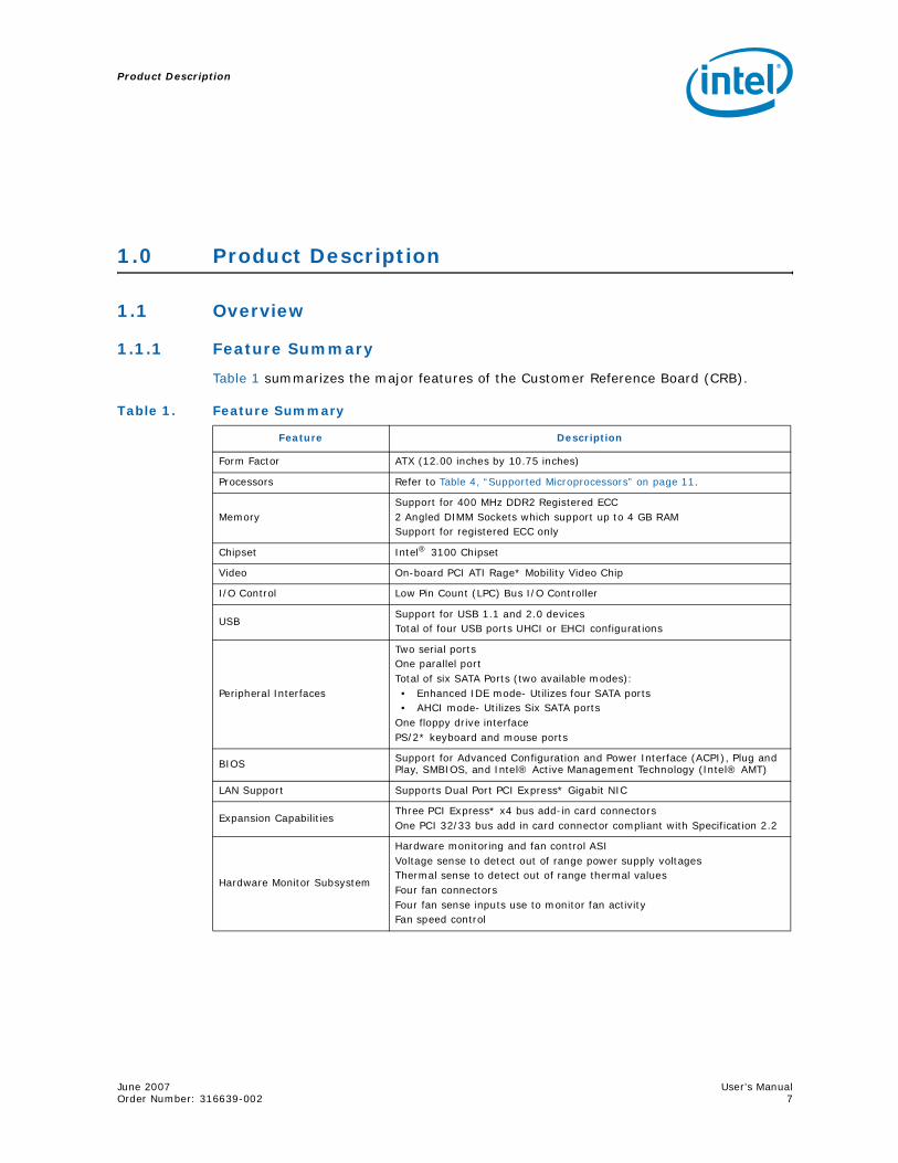
Table 1 summarizes the major features of the Customer Reference Board (CRB).
Table 1. Feature Summary
Feature Description
Form Factor ATX (12.00 inches by 10.75 inches)
Processors Refer to Table 4, “Supported Microprocessors” on page 11.
MemorySupport for 400 MHz DDR2 Registered ECC2 Angled DIMM Sockets which support up to 4 GB RAMSupport for registered ECC only
Chipset Intel® 3100 Chipset
Video On-board PCI ATI Rage* Mobility Video Chip
I/O Control Low Pin Count (LPC) Bus I/O Controller
USBSupport for USB 1.1 and 2.0 devices Total of four USB ports UHCI or EHCI configurations
Peripheral Interfaces
Two serial portsOne parallel portTotal of six SATA Ports (two available modes):• Enhanced IDE mode- Utilizes four SATA ports• AHCI mode- Utilizes Six SATA ports
One floppy drive interfacePS/2* keyboard and mouse ports
BIOS Support for Advanced Configuration and Power Interface (ACPI), Plug and Play, SMBIOS, and Intel® Active Management Technology (Intel® AMT)
LAN Support Supports Dual Port PCI Express* Gigabit NIC
Expansion CapabilitiesThree PCI Express* x4 bus add-in card connectorsOne PCI 32/33 bus add in card connector compliant with Specification 2.2
Hardware Monitor Subsystem
Hardware monitoring and fan control ASIVoltage sense to detect out of range power supply voltagesThermal sense to detect out of range thermal valuesFour fan connectorsFour fan sense inputs use to monitor fan activityFan speed control
Product Description
User’s Manual June 20078 Order Number: 316639-002
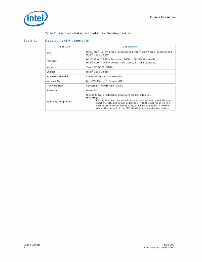
Table 2 describes what is included in the Development Kit.
Table 2. Development Kit Contents
Feature Description
PCB CRB, Intel® Core™ 2 Duo Processor and Intel® Core™ Duo Processor and Intel® 3100 Chipset
ProcessorIntel® CoreTM 2 Duo Processor L7400, 1.50 GHz (installed)Intel® CoreTM Duo Processor ULV U2500, 1.2 Ghz (supplied)
Memory Two 1 GB DDR2 DIMMs
Chipset Intel® 3100 Chipset
Processor Heatsink Coolermaster* Active Heatsink
Network Card Intel PCI Express* Gigabit NIC
Firmware Hub Socketed Firmware Hub (BIOS)
Software Driver CD
Additional Peripherals
Standoffs (with installation hardware) for Benchtop useWarning:
Placing the board on an unknown surface without standoffs may short the CRB and result in damage. If CRB is not mounted in a chassis, Intel recommends using provided Standoffs to prevent risk of the bottom of the CRB shorting on a conductive surface.
June 2007 User’s ManualOrder Number: 316639-002 9
Product Description
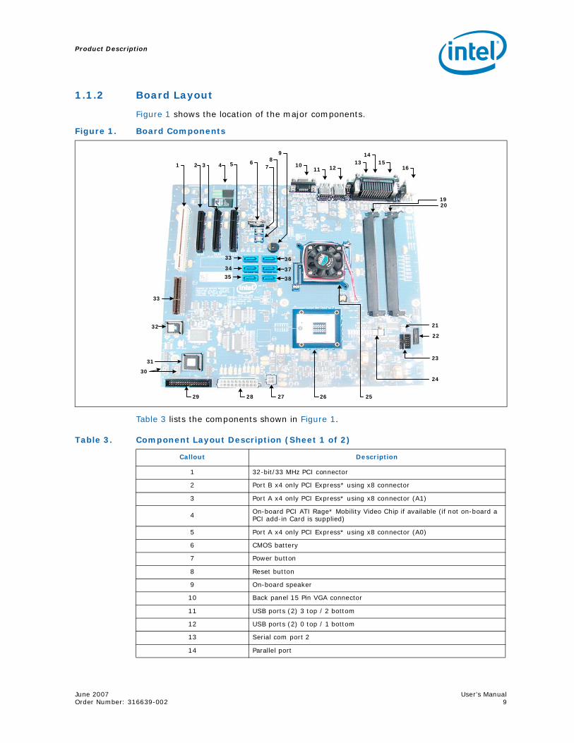
1.1.2 Board Layout
Figure 1 shows the location of the major components.
Table 3 lists the components shown in Figure 1.
Figure 1. Board Components
4
31
1021 3 5 6 89
11 1213
1415
16
1920
24
21
23
22
2526272829
32
33
7
33
34
35
36
37
38
30
Table 3. Component Layout Description (Sheet 1 of 2)
Callout Description
1 32-bit/33 MHz PCI connector
2 Port B x4 only PCI Express* using x8 connector
3 Port A x4 only PCI Express* using x8 connector (A1)
4 On-board PCI ATI Rage* Mobility Video Chip if available (if not on-board a PCI add-in Card is supplied)
5 Port A x4 only PCI Express* using x8 connector (A0)
6 CMOS battery
7 Power button
8 Reset button
9 On-board speaker
10 Back panel 15 Pin VGA connector
11 USB ports (2) 3 top / 2 bottom
12 USB ports (2) 0 top / 1 bottom
13 Serial com port 2
14 Parallel port
Product Description
User’s Manual June 200710 Order Number: 316639-002
15 Serial com port 1
16 PS/2* top = mouse / bottom = keyboard
17 DIMM0 (Not used in This angled DIMM Design, two DIMMS only)
18 DIMM1 (Not used in This angled DIMM Design, two DIMMS only)
19 DIMM2
20 DIMM3 (closest to edge of board)
21 AUX FAN 1
22 XDP connector
23 JTAG connector
24 AUX FAN 0
25 Intel® 3100 Chipset with active fan Connected to FAN1
26 Processor with active fan plugged into processor FAN
27 ATX 12 V for SATA power
28 ATX power connector
29 Floppy drive connector
30 Port 80 seven segment displays
31 Port 80 chip
32 Firmware hub (BIOS)
33 Plug For validation only
34 SATA port 0
35 SATA port 1
36 SATA port 2
37 SATA port 3
38 SATA port 4
39 SATA port 5
Table 3. Component Layout Description (Sheet 2 of 2)
Callout Description
June 2007 User’s ManualOrder Number: 316639-002 11
Product Description
1.2 Processors
The CRB is designed to support the following processors with a 533 and 667 MHz FSB speed.
Use only the processors listed below in Table 4. Use of unsupported processors can damage the CRB, the processor, and the power supply.
Note: In this document Processor refers to all processor SKUs listed in Table 4.
1.3 System Memory
The CRB has two DIMM sockets and supports the following memory features:
• DDR2-400 MHz registered ECC
• SEC/DED
• Up to four ranks of memory
• Minimum total system memory: 512 MB, maximum of 4 GB
• ECC DIMMs, 8 bits ECC
• Single channel operation only
• Supports x4 and x8 DDR2-512 Mb and DDR2-1 Gb technologies and x4 DDR2-2 Gb technologies
1.3.1 DDR2-400 DIMM Slot Populations
Table 5 shows the supported DDR2-400 DIMM populations.
Table 4. Supported Microprocessors
Microprocessor Cores CLK Speed
FSB Speed
L2 Cache TDP
Intel® Core™ 2 Duo Processor L7400 Dual 1.50GHz 667MHz 4MB 17W
Intel® Core™ Duo processor ULV U2500 Dual 1.20GHz 533MHz 2MB 9W
Intel® Celeron® M Processor ULV 423 Single 1.06GHz 533MHz 1MB 5.5W
Table 5. Supported DDR2-400 DIMM Populations
DIMM Configuration DIMM0 DIMM1 DIMM2 DIMM3
1 Single-rank N/A N/A Empty Single-rank
1 Dual-rank N/A N/A Empty Dual-rank
2 Single-rank N/A N/A Single-rank Single-rank
1 Dual-rank, 1 Single-rank N/A N/A Single-rank Dual-rank
2 Dual-rank N/A N/A Dual-rank Dual-rank
Product Description
User’s Manual June 200712 Order Number: 316639-002
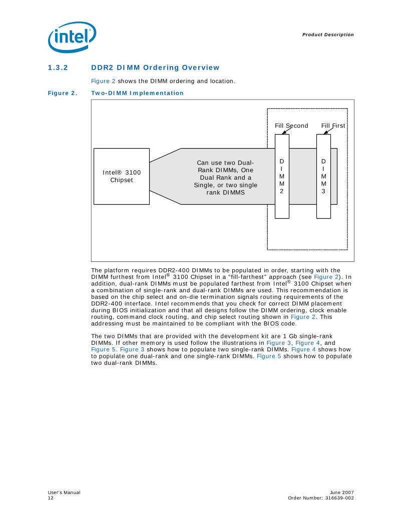
1.3.2 DDR2 DIMM Ordering Overview
Figure 2 shows the DIMM ordering and location.
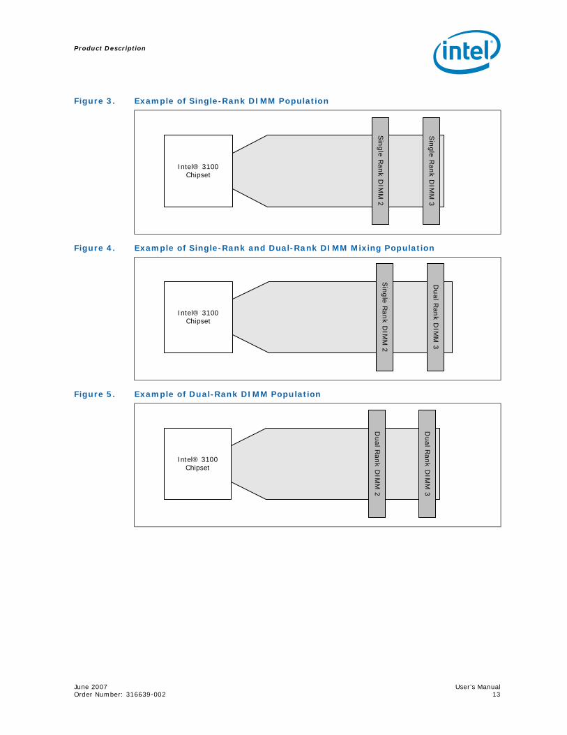
The platform requires DDR2-400 DIMMs to be populated in order, starting with the DIMM furthest from Intel® 3100 Chipset in a “fill-farthest” approach (see Figure 2). In addition, dual-rank DIMMs must be populated farthest from Intel® 3100 Chipset when a combination of single-rank and dual-rank DIMMs are used. This recommendation is based on the chip select and on-die termination signals routing requirements of the DDR2-400 interface. Intel recommends that you check for correct DIMM placement during BIOS initialization and that all designs follow the DIMM ordering, clock enable routing, command clock routing, and chip select routing shown in Figure 2. This addressing must be maintained to be compliant with the BIOS code.
The two DIMMs that are provided with the development kit are 1 Gb single-rank DIMMs. If other memory is used follow the illustrations in Figure 3, Figure 4, and Figure 5. Figure 3 shows how to populate two single-rank DIMMs. Figure 4 shows how to populate one dual-rank and one single-rank DIMMs. Figure 5 shows how to populate two dual-rank DIMMs.
Figure 2. Two-DIMM Implementation
Intel® 3100 Chipset
DIMM3
DIMM2
Fill Second Fill First
Can use two Dual-Rank DIMMs, One Dual Rank and a
Single, or two single rank DIMMS
June 2007 User’s ManualOrder Number: 316639-002 13
Product Description
Figure 3. Example of Single-Rank DIMM Population
Figure 4. Example of Single-Rank and Dual-Rank DIMM Mixing Population
Figure 5. Example of Dual-Rank DIMM Population
Intel® 3100 Chipset
Sin
gle R
ank D
IMM
3
Sin
gle
Rank D
IMM
2
Intel® 3100 Chipset
Dual R
ank D
IMM
3
Sin
gle
Rank D
IMM
2
Intel® 3100 Chipset
Dual R
ank D
IMM
3
Dual R
ank D
IMM
2
Product Description
User’s Manual June 200714 Order Number: 316639-002
1.4 Intel® 3100 Chipset
1.4.1 On-Board Peripherals
Super I/O and PCI Video are included as on-board peripherals.
1.4.1.1 Super I/O
Super I/O includes a Low Pin Count (LPC) driven Super I/O device that can be disabled by removing a resistor.
1.4.1.2 PCI Video
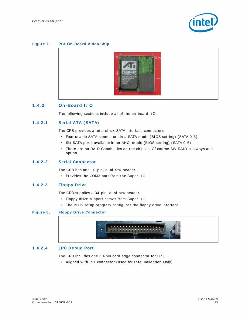
An ATI Rage* Mobility-M integrated video controller is located on the 32-bit, 33 MHz PCI bus. Figure 7, “PCI On-Board Video Chip” on page 15 is a picture of the on board chip.
Figure 6. Intel® 3100 Chipset Block Diagram
B5990-01
FSB
PCI Express*1x8 configurable as 2x4 or 2x1
PCI Express*1x4 or 4x1
Serial ATA6 Drives
LPC
SM Bus x2
PCI 32/33
2 UART
4 USB-2.0
38 GPIOs
WDT
Port APort B
Single-Memory Channel
Registered ECCDDR2 400
EDMA
Intel® 3100 Chipset
IICH IMCH
Processor
* Other names and brands may be claimed as the property of others.
June 2007 User’s ManualOrder Number: 316639-002 15
Product Description
1.4.2 On-Board I/O
The following sections include all of the on-board I/O.
1.4.2.1 Serial ATA (SATA)
The CRB provides a total of six SATA interface connectors.
• Four usable SATA connectors in a SATA mode (BIOS setting) (SATA 0-3)
• Six SATA ports available in an AHCI mode (BIOS setting) (SATA 0-5)
• There are no RAID Capabilities on the chipset. Of course SW RAID is always and option.
1.4.2.2 Serial Connector
The CRB has one 10-pin, dual-row header.
• Provides the COM3 port from the Super I/O
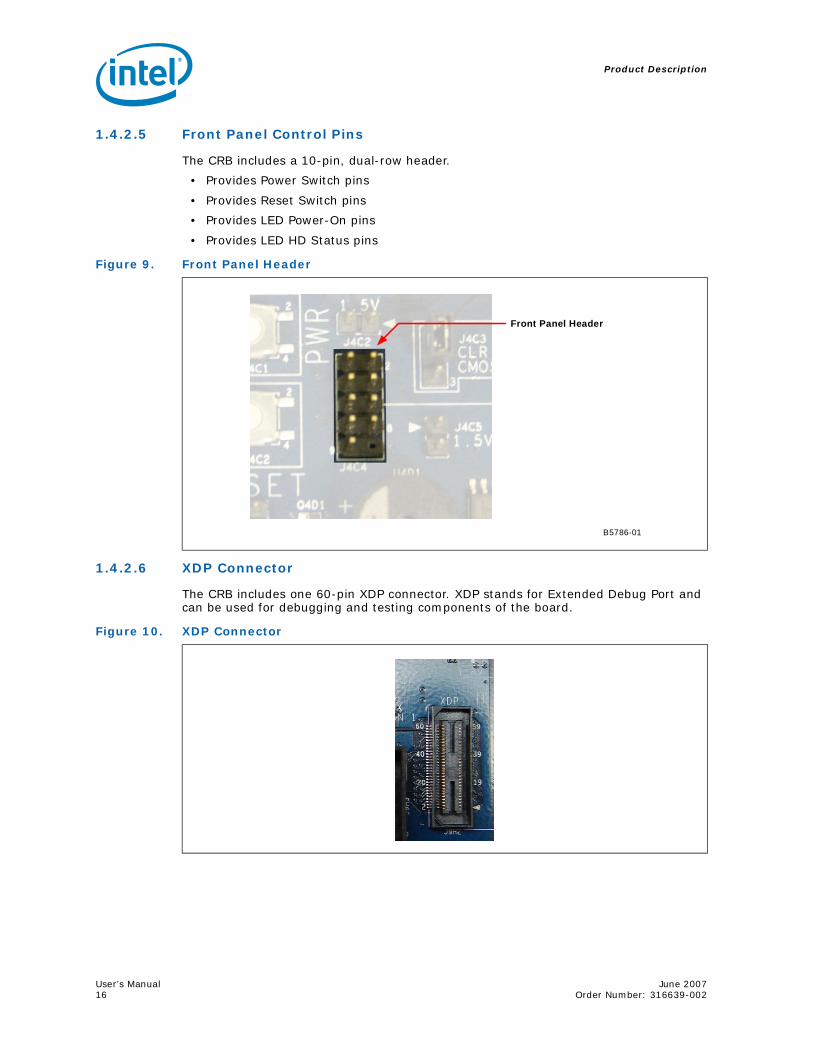
1.4.2.3 Floppy Drive
The CRB supplies a 34-pin, dual-row header.
• Floppy drive support comes from Super I/O
• The BIOS setup program configures the floppy drive interface
1.4.2.4 LPC Debug Port
The CRB includes one 60-pin card edge connector for LPC.
• Aligned with PCI connector (used for Intel Validation Only)
Figure 7. PCI On-Board Video Chip
Figure 8. Floppy Drive Connector
Product Description
User’s Manual June 200716 Order Number: 316639-002
1.4.2.5 Front Panel Control Pins
The CRB includes a 10-pin, dual-row header.
• Provides Power Switch pins
• Provides Reset Switch pins
• Provides LED Power-On pins
• Provides LED HD Status pins
1.4.2.6 XDP Connector
The CRB includes one 60-pin XDP connector. XDP stands for Extended Debug Port and can be used for debugging and testing components of the board.
Figure 9. Front Panel Header
B5786-01
Front Panel Header
Figure 10. XDP Connector
June 2007 User’s ManualOrder Number: 316639-002 17
Product Description
1.4.2.7 USB
The CRB has a 10-pin, dual-row header to route two USB Ports to an external USB connector.
• Allows two USB 1.1 or 2.0 ports to be routed to the dual-stack rear I/O or optionally to the 10-pin header from the internal I/O. These USB ports are Port 2 and Port 3. Rear panel ports 2 and 3 are not simultaneously functional.
• By default, routing for USB is to the dual-stack header on the rear panel I/O.
• In conjunction with the rear panel USB Ports there are only a total of four USB ports.
More information is available in Section 1.4.4.3, “USB Ports” on page 18.
1.4.3 I/O Slots for Expansion Capabilities
1.4.3.1 PCI Express*
The CRB provides a total of 3 x4 PCI Express* ports.
• Port A provides two x4 connections through two x8 connectors
• Port B provides one x4 connection through one x8 connector
• 32-bit ECRC (Port A only) stays with packet ensuring correct data at destination
• 256 opportunistic combining for read completions to improve performance
• ONLY Port A provides posted writes between each x4 port
• ONLY Port A provides memory-to-I/O DMA
Note: The PCI Express* Ports are x8 connectors, but ONLY have the functionality of a x4 connector. This enables you to use a x8 card on the CRB but it has the bandwidth and functionality of the x4.
Warning: Hot-Plug is NOT supported on this platform.
1.4.3.2 PCI
The CRB provides one PCI slot. It has the following characteristics:
• Specification 2.2 compliant
• 32-bit
• 33 MHz
• 120 MB/s throughput
• 64-bit addressing through the DAC protocol
Product Description
User’s Manual June 200718 Order Number: 316639-002
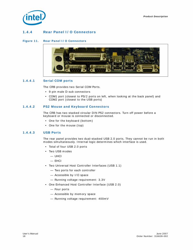
1.4.4 Rear Panel I/O Connectors
1.4.4.1 Serial COM ports
The CRB provides two Serial COM Ports.
• 9-pin male D-sub connectors
• COM1 port (closest to PS/2 ports on left, when looking at the back panel) and COM2 port (closest to the USB ports)
1.4.4.2 PS2 Mouse and Keyboard Connectors
The CRB has two stacked circular DIN PS2 connectors. Turn off power before a keyboard or mouse is connected or disconnected.
• One for the keyboard (bottom)
• One for the mouse (top)
1.4.4.3 USB Ports
The rear panel provides two dual-stacked USB 2.0 ports. They cannot be run in both modes simultaneously. Internal logic determines which interface is used.
• Total of four USB 2.0 ports
• Two USB modes
— UHCI
— EHCI
• Two Universal Host Controller Interfaces (USB 1.1)
— Two ports for each controller
— Accessible by I/O space
— Running voltage requirement: 3.3V
• One Enhanced Host Controller Interface (USB 2.0)
— Four ports
— Accessible by memory space
— Running voltage requirement: 400mV
Figure 11. Rear Panel I/O Connectors
June 2007 User’s ManualOrder Number: 316639-002 19
Product Description
1.4.4.4 Parallel Port
The CRB provides one parallel port on the rear panel. The Parallel Port can be viewed in Figure 11, “Rear Panel I/O Connectors” on page 18
• 25-pin female D-sub connector (above COM ports)
1.4.4.5 VGA Port
The CRB provides one VGA connector for on-board video.
• 15-pin male D-sub connector
• On-board ATI RAGE Mobility PCI video
• If no “on-board Video”, a PCI video card is supplied with kit
1.4.5 Hardware Server Management Features
The CRB provides several server management features like a voltage monitor and temperature monitor. It also provides control for overall protection of the platform.
1.4.5.1 Voltage Monitor
The CRB uses a Heceta* 7 (LM93) to monitor and communicate through the SMBus.
1.4.5.2 Watch Dog Timer (WDT)
The Watch Dog Timer (WDT) provides output from the Intel® 3100 Chipset to generate one of the following:
• PCI_RESET
• Illuminate an LED
1.4.5.3 Sleep States and Soft Off
• S0, S3 and S5 sleep states
• Soft off capability (S5)
— Operating system dependent
— Requires a complete OS boot when the system wakes
1.4.5.4 Wake Events
• Power switch
1.4.5.5 Hardware Clock Throttling
• Provides support for hardware clock throttling through STOPCLK#
Product Description
User’s Manual June 200720 Order Number: 316639-002
1.4.5.6 Fan Power Connection
• Direct +12 V DC power connectors
• One processor fan connector (CPUFAN)
• One fan for Intel® 3100 Chipset (Fan1)
• Two auxiliary fan connectors (AUXFAN)
1.4.5.7 On Board Switches
The CRB has the following momentary push button switches to provide state control:
• Power
• Reset
• Wake (this button is not functional)
• Port 80/81
1.4.5.8 Trusted Platform Module (TPM)
The Trusted Platform Module (TPM) is a component of the platform that is specifically designed to enhance platform security above and beyond the capabilities of today’s software. It provides protected space for key operations and other security critical tasks. Using both hardware and software, the TPM protects encryption and signature keys at their most vulnerable stages of operation, for instance, when the keys are being used in an unencrypted plain text form. The TPM is specifically designed to shield unencrypted keys and platform authentication information from software-based attacks.
1.5 Supported Operating Systems
The CRB is validated with the following operating systems:
• DOS
— BIOS supports the installation and booting of the DOS* 6.22 operating system
• Linux*
— BIOS supports the installation and booting of both Red Hat Enterprise Linux* Version 3 and 4 and Linux Monta Vista Pro* and Monta Vista Carrier*.
• QNX*
• Microsoft Windows XP*
• Microsoft Embedded XP*
• Microsoft Windows Vista* (once available)
• Microsoft Windows Server 2003*
• Free BSD
Note: Operating systems are to be purchased by the customer and are not distributed with this development kit.
June 2007 User’s ManualOrder Number: 316639-002 21
Product Description
1.6 Supported BIOS Features
The BIOS has an AMI* core with the following components:
1.6.1 ACPI
ACPI gives the OS direct control over the power management and plug-and-play functions of the platform. The use of ACPI with this CRB requires an OS that provides full ACPI support.
Table 6. Supported BIOS Features
Name of BIOS component Description
PCI 2.3 The BIOS is PCI 2.3 compliant.
SCSI boot The BIOS supports booting from a plug in SCSI device, if present.
LAN boot The BIOS supports booting from a plug in Ethernet device, if present.
Fiber-channel boot The BIOS supports booting from a plug in fiber-channel device, if present.
Serial ATA boot The BIOS supports booting from a Serial ATA hard drive.
CD-ROM boot The BIOS supports booting from a Serial ATA CD-ROM.
USB boot The BIOS supports booting from a USB boot device.
Floppy boot The BIOS supports booting from a floppy drive
PXH The BIOS initializes and supports a PXH riser card if it is plugged into a PCI-E* slot on the CRB.
PCI Express* The BIOS initializes and supports PCI Express* cards that are plugged into the CRB.
USB The BIOS supports the USB 1.1 and USB 2.0 interfaces.
CMOS Header The BIOS supports recognizing the clear CMOS header.
ECC support The BIOS detects and supports ECC memory.
Watchdog Timer (WDT) The BIOS provides watch dog timer support.
APIC and ACPI Control
The ability to enable and disable APIC and ACPI is present in the BIOS. Control is also required for OS plug and play features. The BIOS supports the following ACPI states:• G0(S0) – Working• G1(S3) – Sleeping [Suspend to RAM]• G2(S5) – Soft Off
The BIOS supports C0, C1, C1E and C2 states.
Patch Update Mechanism The Patch Update Mechanism is used to upgrade and/or install micro-code patches into BIOS is supported.
FSB Error Handling Control The BIOS has the capability to enable and/or disable FSB error handling.
Table 7. Effects of Pressing the Power Switch (Sheet 1 of 2)
If the System is in this state... ...and the power switch is pressed for
...the system enters this state
Off(ACPI G2/G5 - soft off)
Less than four secondPower-on(ACPI G0 - working state)
On(ACPI G0 - working state)
Less than four secondsSoft-off/Standby(ACPI G1 - sleeping state)
Product Description
User’s Manual June 200722 Order Number: 316639-002
1.6.1.1 System States and Power States
Under ACPI, the OS directs all system and device power state transitions by managing devices in and out of low-power states based on user preferences and knowledge of how devices are being used by applications. Devices that are not being used can be turned off. The OS uses information from applications and user settings to put the system as a whole into a low-power state.
1.7 Power Supply
The platform may not come with a power supply. If one is not provided please use a standard off-the-shelf ATX12V power supply with a power rating of 450 W. (Customer may use a smaller power supply as this is more power than necessary. This CRB total system power is typically running at less then 100 W.)
1.8 Thermal and Mechanical Components
On (ACPI G0 - working state)
More than four secondsFail Safe Power-off(ACPI G2/G5 - soft off)
Sleep(ACPI G1 - sleeping state)
Less than four secondsWake-up(ACPI G0 - working state)
Sleep(ACPI G1 - sleeping state)
More than four secondsPower-off(ACPI G2/G5 - soft off)
Table 7. Effects of Pressing the Power Switch (Sheet 2 of 2)
If the System is in this state... ...and the power switch is pressed for
...the system enters this state
Table 8. Thermal and Mechanical Components
Name Description
Standard Processor Thermal Solution Mounting
The CRB supports full power processor thermal solution mounting provisions as deleanated in the processor thermal design guide.
Processor Fan The CRB provides a fan header for the processor that includes 12 V with tachometer.
Intel® 3100 Chipset Heatsink The CRB supports the Intel® 3100 Chipset heatsink mounting requirements.
Active Intel® 3100 Chipset Heatsink The CRB provides mounting provisions and a fan header for an active Intel® 3100 Chipset thermal solution.
Power Measurement
The CRB provides a means for power measurement for the following components:• Processor• Intel® 3100 Chipset• DDR2
Fan Headers The CRB provides three fan headers.
Solder Down Anchors The CRB provides solder down anchors for the Intel® 3100 Chipset. The Intel® 3100 Chipset includes active heatsink mounting holes.
Iso-chiller Attachment
The iso-chiller attachment for the processor uses the iso-chiller kit and should be mounted using the standard heatsink mounting holes. The Intel® 3100 Chipset uses the iso-chiller kit and has active heatsink mounting holes for attachment.
June 2007 User’s ManualOrder Number: 316639-002 23
Product Description
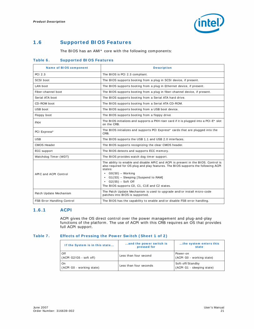
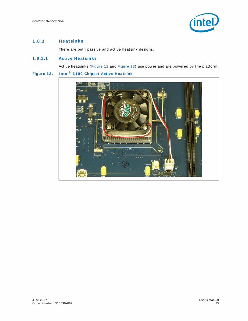
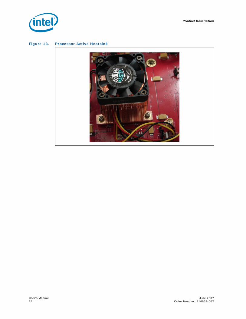
1.8.1 Heatsinks
There are both passive and active heatsink designs.
1.8.1.1 Active Heatsinks
Active heatsinks (Figure 12 and Figure 13) use power and are powered by the platform.
Figure 12. Intel® 3100 Chipset Active Heatsink
Product Description
User’s Manual June 200724 Order Number: 316639-002
Figure 13. Processor Active Heatsink
June 2007 User’s ManualOrder Number: 316639-002 25
Product Description
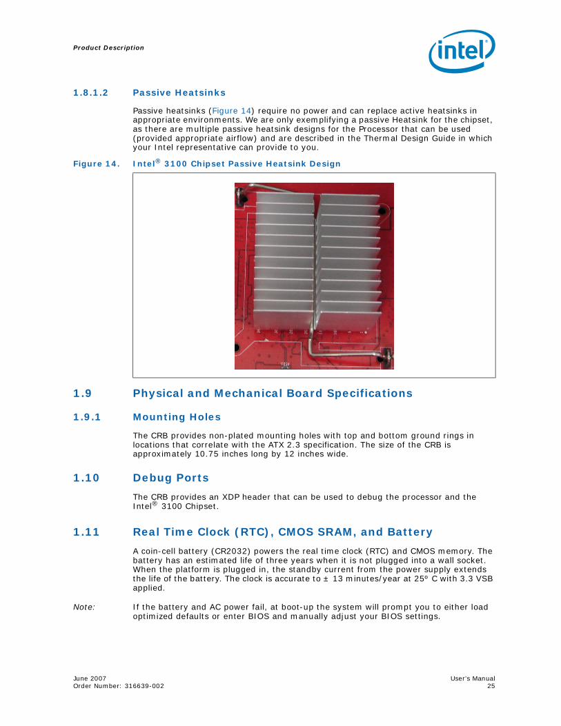
1.8.1.2 Passive Heatsinks
Passive heatsinks (Figure 14) require no power and can replace active heatsinks in appropriate environments. We are only exemplifying a passive Heatsink for the chipset, as there are multiple passive heatsink designs for the Processor that can be used (provided appropriate airflow) and are described in the Thermal Design Guide in which your Intel representative can provide to you.
1.9 Physical and Mechanical Board Specifications
1.9.1 Mounting Holes
The CRB provides non-plated mounting holes with top and bottom ground rings in locations that correlate with the ATX 2.3 specification. The size of the CRB is approximately 10.75 inches long by 12 inches wide.
1.10 Debug Ports
The CRB provides an XDP header that can be used to debug the processor and the Intel® 3100 Chipset.
1.11 Real Time Clock (RTC), CMOS SRAM, and Battery
A coin-cell battery (CR2032) powers the real time clock (RTC) and CMOS memory. The battery has an estimated life of three years when it is not plugged into a wall socket. When the platform is plugged in, the standby current from the power supply extends the life of the battery. The clock is accurate to ± 13 minutes/year at 25º C with 3.3 VSB applied.
Note: If the battery and AC power fail, at boot-up the system will prompt you to either load optimized defaults or enter BIOS and manually adjust your BIOS settings.
Figure 14. Intel® 3100 Chipset Passive Heatsink Design
Platform Setup
User’s Manual June 200726 Order Number: 316639-002
2.0 Platform Setup
Note: Before connecting power make sure that the CRB (Customer Reference Board) is either mounted in a chassis or is on a non-conductive surface to prevent grounding. Ensure a safe work environment. Make sure you are in a static-free environment. Before removing any components from their anti-static packaging. The evaluation board is susceptible to electrostatic discharge, which may cause product failure or unpredictable operation.
Caution: Connecting the wrong cable or reversing a cable may damage the evaluation board and may damage the device being connected. Since the board is not in a protective chassis, use caution when connecting cables to this product.
2.1 Connecting the Wires
Note: When you receive the CRB, all jumpers are correctly set and it is ready to boot.
June 2007 User’s ManualOrder Number: 316639-002 27
Platform Setup
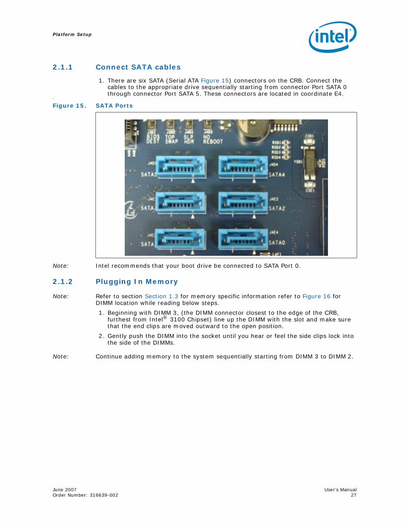
2.1.1 Connect SATA cables
1. There are six SATA (Serial ATA Figure 15) connectors on the CRB. Connect the cables to the appropriate drive sequentially starting from connector Port SATA 0 through connector Port SATA 5. These connectors are located in coordinate E4.
P
Note: Intel recommends that your boot drive be connected to SATA Port 0.
2.1.2 Plugging In Memory
Note: Refer to section Section 1.3 for memory specific information refer to Figure 16 for DIMM location while reading below steps.
1. Beginning with DIMM 3, (the DIMM connector closest to the edge of the CRB, furthest from Intel® 3100 Chipset) line up the DIMM with the slot and make sure that the end clips are moved outward to the open position.
2. Gently push the DIMM into the socket until you hear or feel the side clips lock into the side of the DIMMs.
Note: Continue adding memory to the system sequentially starting from DIMM 3 to DIMM 2.
Figure 15. SATA Ports
Platform Setup
User’s Manual June 200728 Order Number: 316639-002
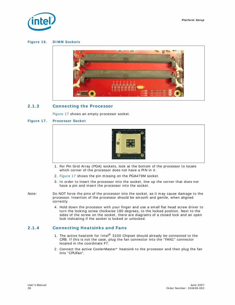
2.1.3 Connecting the Processor
Figure 17 shows an empty processor socket.
1. For Pin Grid Array (PGA) sockets, look at the bottom of the processor to locate which corner of the processor does not have a PIN in it.
2. Figure 17 shows the pin missing on the PGA479M socket.
3. In order to insert the processor into the socket, line up the corner that does not have a pin and insert the processor into the socket.
Note: Do NOT force the pins of the processor into the socket, as it may cause damage to the processor. Insertion of the processor should be smooth and gentle, when aligned correctly.
4. Hold down the processor with your finger and use a small flat head screw driver to turn the locking screw clockwise 180 degrees, to the locked position. Next to the sides of the screw on the socket, there are diagrams of a closed lock and an open lock indicating if the socket is locked or unlocked.
2.1.4 Connecting Heatsinks and Fans
1. The active heatsink for Intel® 3100 Chipset should already be connected to the CRB. If this is not the case, plug the fan connector into the “FAN1” connector located in the coordinate F7.
2. Connect the active CoolerMaster* heatsink to the processor and then plug the fan into “CPUFan”.
Figure 16. DIMM Sockets
Figure 17. Processor Socket
June 2007 User’s ManualOrder Number: 316639-002 29
Platform Setup
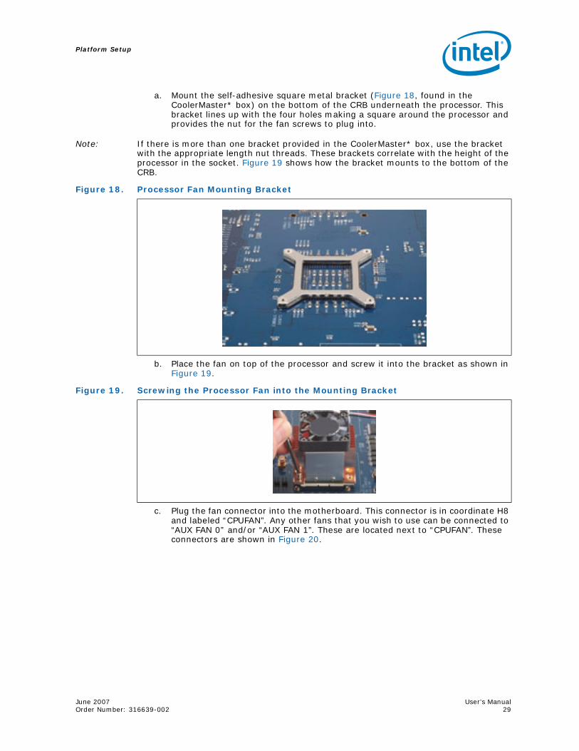
a. Mount the self-adhesive square metal bracket (Figure 18, found in the CoolerMaster* box) on the bottom of the CRB underneath the processor. This bracket lines up with the four holes making a square around the processor and provides the nut for the fan screws to plug into.
Note: If there is more than one bracket provided in the CoolerMaster* box, use the bracket with the appropriate length nut threads. These brackets correlate with the height of the processor in the socket. Figure 19 shows how the bracket mounts to the bottom of the CRB.
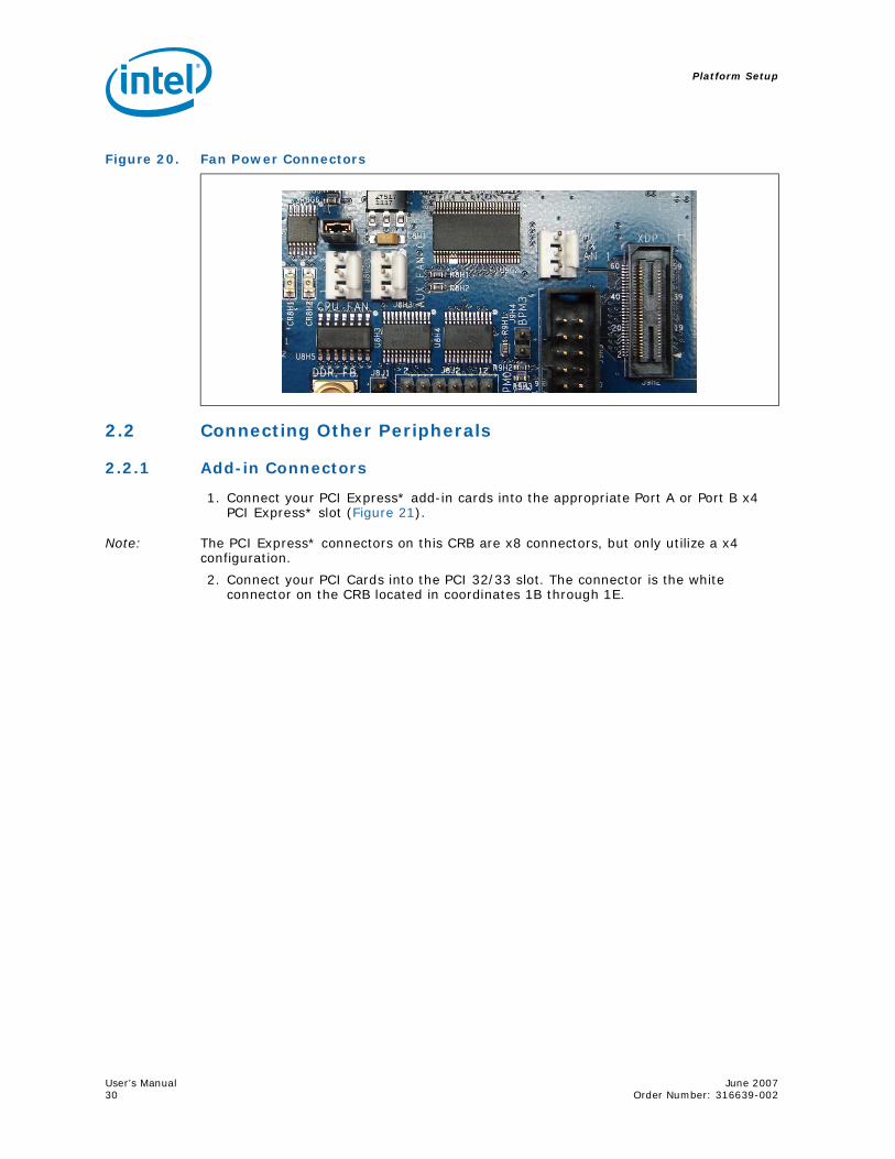
b. Place the fan on top of the processor and screw it into the bracket as shown in Figure 19.
c. Plug the fan connector into the motherboard. This connector is in coordinate H8 and labeled “CPUFAN”. Any other fans that you wish to use can be connected to “AUX FAN 0” and/or “AUX FAN 1”. These are located next to “CPUFAN”. These connectors are shown in Figure 20.
Figure 18. Processor Fan Mounting Bracket
Figure 19. Screwing the Processor Fan into the Mounting Bracket
Platform Setup
User’s Manual June 200730 Order Number: 316639-002
2.2 Connecting Other Peripherals
2.2.1 Add-in Connectors
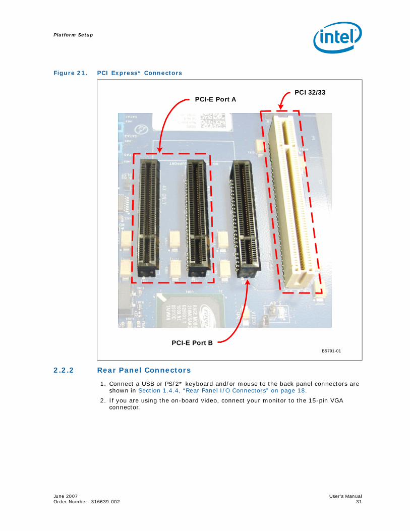
1. Connect your PCI Express* add-in cards into the appropriate Port A or Port B x4 PCI Express* slot (Figure 21).
Note: The PCI Express* connectors on this CRB are x8 connectors, but only utilize a x4 configuration.
2. Connect your PCI Cards into the PCI 32/33 slot. The connector is the white connector on the CRB located in coordinates 1B through 1E.
Figure 20. Fan Power Connectors
June 2007 User’s ManualOrder Number: 316639-002 31
Platform Setup
2.2.2 Rear Panel Connectors
1. Connect a USB or PS/2* keyboard and/or mouse to the back panel connectors are shown in Section 1.4.4, “Rear Panel I/O Connectors” on page 18.
2. If you are using the on-board video, connect your monitor to the 15-pin VGA connector.
Figure 21. PCI Express* Connectors
B5791-01
PCI-E Port A
PCI-E Port B
PCI 32/33
Platform Setup
User’s Manual June 200732 Order Number: 316639-002
2.2.3 Connecting a Floppy Drive
In order to connect a floppy drive, plug the cable into the socket shown in Figure 22 by guiding the keyed plug into the keyed socket. Connect the other end of this cable to the floppy drive and providing it power from the power supply.
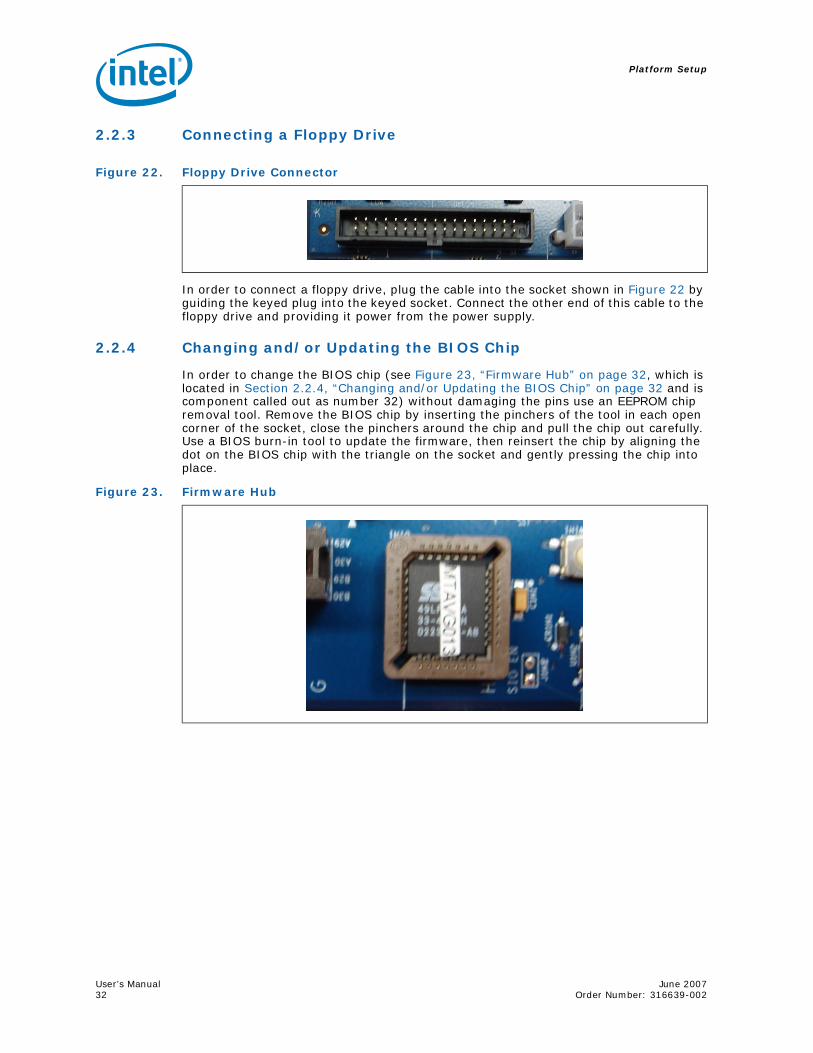
2.2.4 Changing and/or Updating the BIOS Chip
In order to change the BIOS chip (see Figure 23, “Firmware Hub” on page 32, which is located in Section 2.2.4, “Changing and/or Updating the BIOS Chip” on page 32 and is component called out as number 32) without damaging the pins use an EEPROM chip removal tool. Remove the BIOS chip by inserting the pinchers of the tool in each open corner of the socket, close the pinchers around the chip and pull the chip out carefully. Use a BIOS burn-in tool to update the firmware, then reinsert the chip by aligning the dot on the BIOS chip with the triangle on the socket and gently pressing the chip into place.
Figure 22. Floppy Drive Connector
Figure 23. Firmware Hub
June 2007 User’s ManualOrder Number: 316639-002 33
Platform Setup
2.2.5 Changing the CMOS Battery and Clearing CMOS
2.2.5.1 Changing the battery
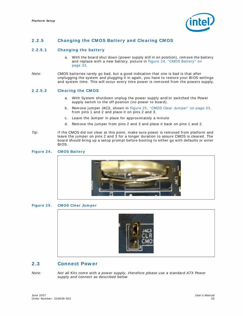
a. With the board shut down (power supply still in on position), remove the battery and replace with a new battery. picture in Figure 24, “CMOS Battery” on page 33.
Note: CMOS batteries rarely go bad, but a good indication that one is bad is that after unplugging the system and plugging it in again, you have to restore your BIOS settings and system time. This will occur every time power is removed from the powers supply.
2.2.5.2 Clearing the CMOS
a. With System shutdown unplug the power supply and/or switched the Power supply switch to the off position (no power to board).
b. Remove jumper J4C3, shown in Figure 25, “CMOS Clear Jumper” on page 33. from pins 1 and 2 and place it on pins 2 and 3.
c. Leave the Jumper in place for approximately a minute
d. Remove the jumper from pins 2 and 3 and place it back on pins 1 and 2.
Tip: If the CMOS did not clear at this point, make sure power is removed from platform and leave the jumper on pins 2 and 3 for a longer duration to assure CMOS is cleared. The board should bring up a setup prompt before booting to either go with defaults or enter BIOS.
2.3 Connect Power
Note: Not all Kits come with a power supply, therefore please use a standard ATX Power supply and connect as described below
Figure 24. CMOS Battery
Figure 25. CMOS Clear Jumper
Platform Setup
User’s Manual June 200734 Order Number: 316639-002
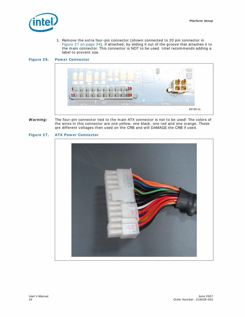
1. Remove the extra four-pin connector (shown connected to 20 pin connector in Figure 27 on page 34), if attached, by sliding it out of the groove that attaches it to the main connector. This connector is NOT to be used. Intel recommends adding a label to prevent use.
Warning: The four-pin connector tied to the main ATX connector is not to be used! The colors of the wires in this connector are one yellow, one black, one red and one orange. These are different voltages then used on the CRB and will DAMAGE the CRB if used.
Figure 26. Power Connector
Figure 27. ATX Power Connector
B5790-01
11
1111
1010
2020
11 22
33 44
June 2007 User’s ManualOrder Number: 316639-002 35
Platform Setup
2. Plug the main connector into the motherboard located in coordinate K3-4 making sure that the plug clip lines up with the clip lock and the connector pins fit easily into their appropriate slots.
Warning: Do NOT force the ATX power plug into the connector, it should go in easily when plugged in correctly. Plugging it in incorrectly will result in severe DAMAGE to the CRB.
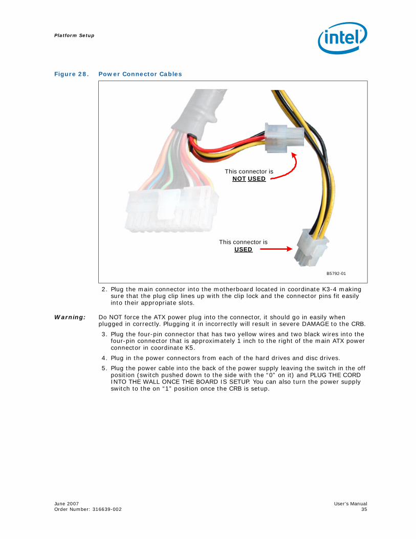
3. Plug the four-pin connector that has two yellow wires and two black wires into the four-pin connector that is approximately 1 inch to the right of the main ATX power connector in coordinate K5.
4. Plug in the power connectors from each of the hard drives and disc drives.
5. Plug the power cable into the back of the power supply leaving the switch in the off position (switch pushed down to the side with the “0” on it) and PLUG THE CORD INTO THE WALL ONCE THE BOARD IS SETUP. You can also turn the power supply switch to the on “1” position once the CRB is setup.
Figure 28. Power Connector Cables
B5792-01
This connector isNOT USED
This connector isUSED
Platform Setup
User’s Manual June 200736 Order Number: 316639-002
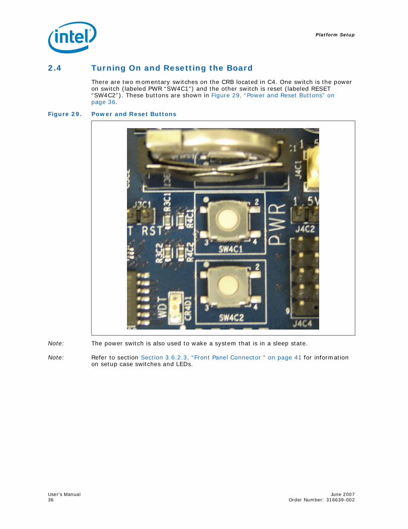
2.4 Turning On and Resetting the Board
There are two momentary switches on the CRB located in C4. One switch is the power on switch (labeled PWR “SW4C1”) and the other switch is reset (labeled RESET “SW4C2”). These buttons are shown in Figure 29, “Power and Reset Buttons” on page 36.
Note: The power switch is also used to wake a system that is in a sleep state.
Note: Refer to section Section 3.6.2.3, “Front Panel Connector ” on page 41 for information on setup case switches and LEDs.
Figure 29. Power and Reset Buttons
June 2007 User’s ManualOrder Number: 316639-002 37
Technical Reference
3.0 Technical Reference
3.1 Memory Resources
Detailed memory information for addressable memory and memory maps can be found in the Intel® 3100 Chipset External Design Specification.
3.2 DMA Channels
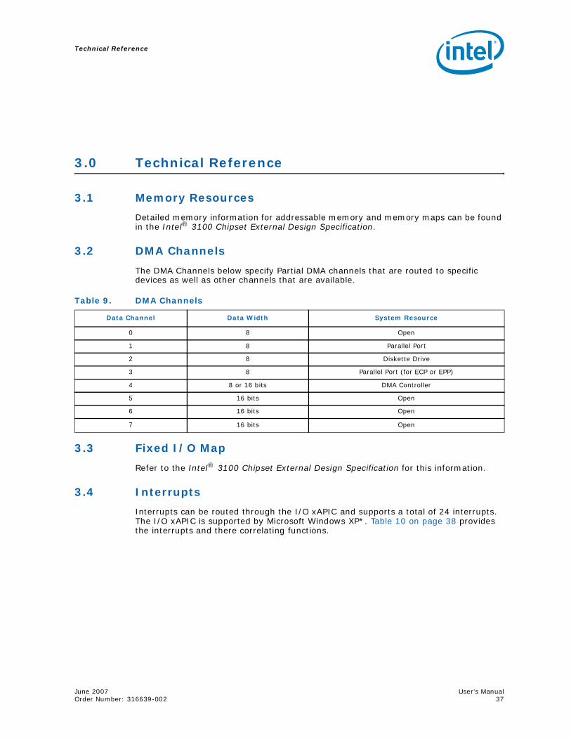
The DMA Channels below specify Partial DMA channels that are routed to specific devices as well as other channels that are available.
3.3 Fixed I/O Map
Refer to the Intel® 3100 Chipset External Design Specification for this information.
3.4 Interrupts
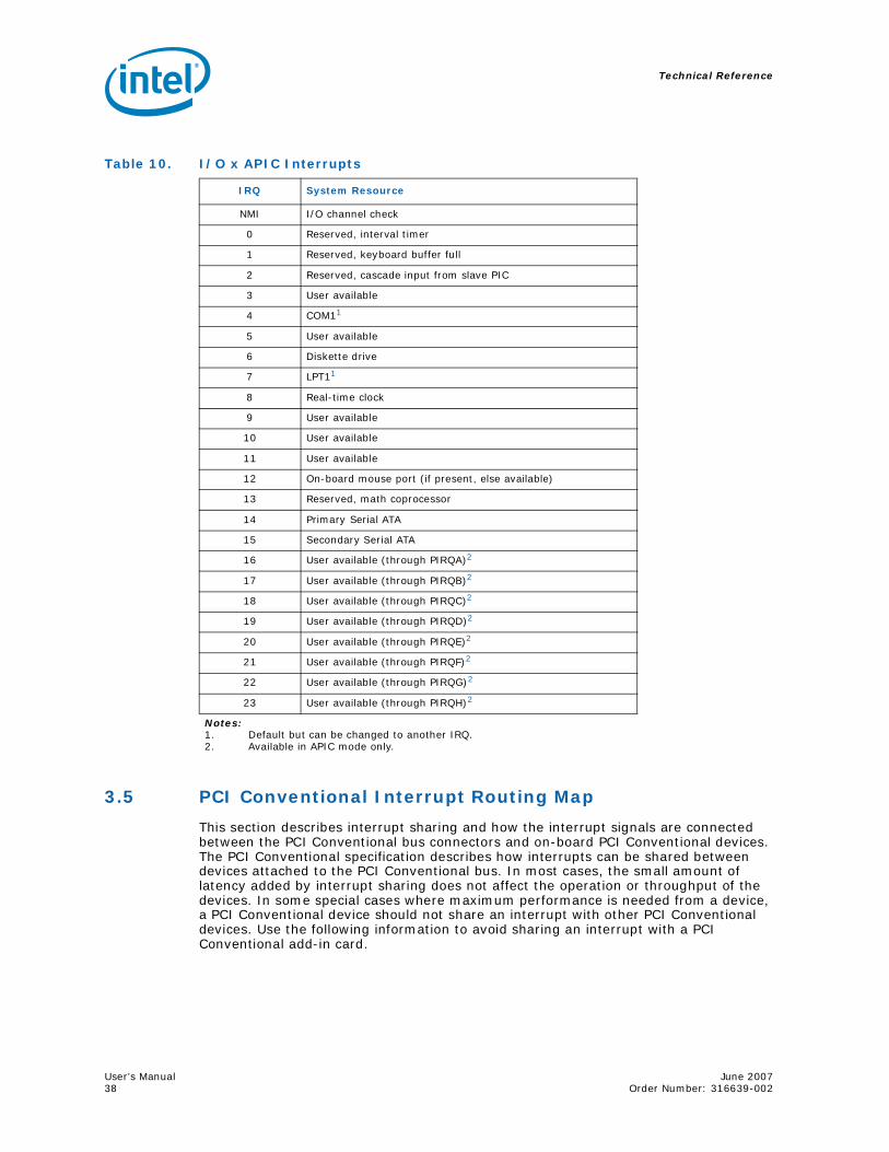
Interrupts can be routed through the I/O xAPIC and supports a total of 24 interrupts. The I/O xAPIC is supported by Microsoft Windows XP*. Table 10 on page 38 provides the interrupts and there correlating functions.
Table 9. DMA Channels
Data Channel Data Width System Resource
0 8 Open
1 8 Parallel Port
2 8 Diskette Drive
3 8 Parallel Port (for ECP or EPP)
4 8 or 16 bits DMA Controller
5 16 bits Open
6 16 bits Open
7 16 bits Open
Technical Reference
User’s Manual June 200738 Order Number: 316639-002
3.5 PCI Conventional Interrupt Routing Map
This section describes interrupt sharing and how the interrupt signals are connected between the PCI Conventional bus connectors and on-board PCI Conventional devices. The PCI Conventional specification describes how interrupts can be shared between devices attached to the PCI Conventional bus. In most cases, the small amount of latency added by interrupt sharing does not affect the operation or throughput of the devices. In some special cases where maximum performance is needed from a device, a PCI Conventional device should not share an interrupt with other PCI Conventional devices. Use the following information to avoid sharing an interrupt with a PCI Conventional add-in card.
Table 10. I/O x APIC Interrupts
IRQ System Resource
NMI I/O channel check
0 Reserved, interval timer
1 Reserved, keyboard buffer full
2 Reserved, cascade input from slave PIC
3 User available
4 COM11
5 User available
6 Diskette drive
7 LPT11
8 Real-time clock
9 User available
10 User available
11 User available
12 On-board mouse port (if present, else available)
13 Reserved, math coprocessor
14 Primary Serial ATA
15 Secondary Serial ATA
16 User available (through PIRQA)2
17 User available (through PIRQB)2
18 User available (through PIRQC)2
19 User available (through PIRQD)2
20 User available (through PIRQE)2
21 User available (through PIRQF)2
22 User available (through PIRQG)2
23 User available (through PIRQH)2
Notes:1. Default but can be changed to another IRQ.2. Available in APIC mode only.
June 2007 User’s ManualOrder Number: 316639-002 39
Technical Reference
3.6 Connectors
Warning: Only the following connectors have over-current protection: back panel USB, front panel USB, and PS/2* connector.
The other internal connectors are not over-current protected and should connect only to devices inside the computer’s chassis, such as fans and internal peripherals. Do not use these connectors to power devices external to the computer’s chassis. A fault in the load presented by the external devices can damage the computer, the power cable, and the external devices. This section describes the connectors. The connectors can be divided into these groups:
• Back panel connectors
• Component side connectors
3.6.1 Back Panel Connectors
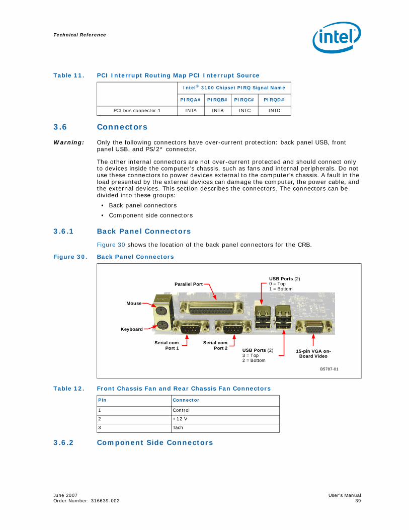
Figure 30 shows the location of the back panel connectors for the CRB.
3.6.2 Component Side Connectors
Table 11. PCI Interrupt Routing Map PCI Interrupt Source
Intel® 3100 Chipset PIRQ Signal Name
PIRQA# PIRQB# PIRQC# PIRQD#
PCI bus connector 1 INTA INTB INTC INTD
Figure 30. Back Panel Connectors
Table 12. Front Chassis Fan and Rear Chassis Fan Connectors
Pin Connector
1 Control
2 +12 V
3 Tach
B5787-01
Mouse
Keyboard
Parallel Port
Serial com Port 1 USB Ports (2)
3 = Top2 = Bottom
Serial com Port 2
USB Ports (2)0 = Top1 = Bottom
15-pin VGA on-Board Video
Technical Reference
User’s Manual June 200740 Order Number: 316639-002
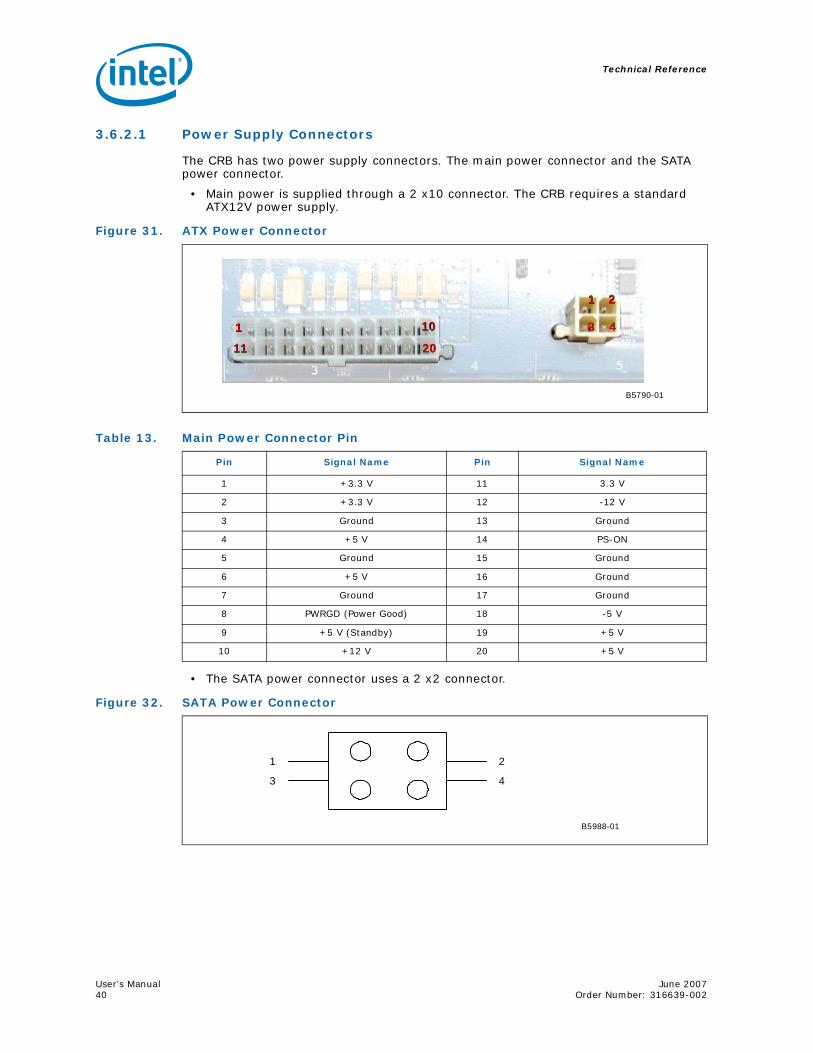
3.6.2.1 Power Supply Connectors
The CRB has two power supply connectors. The main power connector and the SATA power connector.
• Main power is supplied through a 2 x10 connector. The CRB requires a standard ATX12V power supply.
• The SATA power connector uses a 2 x2 connector.
Figure 31. ATX Power Connector
Table 13. Main Power Connector Pin
Pin Signal Name Pin Signal Name
1 +3.3 V 11 3.3 V
2 +3.3 V 12 -12 V
3 Ground 13 Ground
4 +5 V 14 PS-ON
5 Ground 15 Ground
6 +5 V 16 Ground
7 Ground 17 Ground
8 PWRGD (Power Good) 18 -5 V
9 +5 V (Standby) 19 +5 V
10 +12 V 20 +5 V
B5790-01
11
1111
1010
2020
11 22
33 44
Figure 32. SATA Power Connector
B5988-01
2
4
1
3
June 2007 User’s ManualOrder Number: 316639-002 41
Technical Reference
3.6.2.2 Add-in Card Connectors
The CRB has the following add-in card connectors:
• 2 x4 PCI Express* slots which are Port A
• 1 x4 PCI Express* slot which is Port B
• 1 32-bit PCI slot
3.6.2.3 Front Panel Connector
This section describes the functions of the front panel connector. Table 16 lists the signal names of the front panel connector. Figure 33 is a connection diagram for the front panel connector.
Table 14. SATA Power Connector
Pin Signal Name Pin Signal Name
1 GND 3 12 V
2 GND 4 12 V
Table 15. Auxiliary Front Panel Power and Reset Connector Pin
Pin Signal Name In/Out Description
1 HDR_BLNK_GRN Out Front panel green LED
2 Not connected
3 HDR_BLNK_YEL Out Front panel yellow LED
Figure 33. Front Panel Connector
Table 16. Front Panel Connector
Pin Signal Name In/Output Description
1 HD_ACT_LED_P OUT Power side of hard drive activity LED
2 HD_ACT_LED_N OUT Ground side of hard drive activating LED
3 FRNTPNL_PWR_LED POWER OUT Power side of power on LED
4 FRNTPNL_PWR_LED Ground OUT Ground
5 Power Button pin (1) Power Button Pin
6 FP_PWR_BTN_N (2) Power Button Pin 2
B5987-01
2
4
6
8
1
3
5
7
9
Technical Reference
User’s Manual June 200742 Order Number: 316639-002
7 FP_RST_BTN_N IN Pin (1) for Reset Button
8 Reset Ground pin out Pin(2) for reset Button
9 Ground Ground
Table 16. Front Panel Connector
June 2007 User’s ManualOrder Number: 316639-002 43
Technical Reference
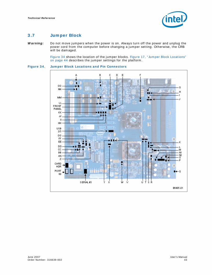
3.7 Jumper Block
Warning: Do not move jumpers when the power is on. Always turn off the power and unplug the power cord from the computer before changing a jumper setting. Otherwise, the CRB will be damaged.
Figure 34 shows the location of the jumper blocks. Figure 17, “Jumper Block Locations” on page 44 describes the jumper settings for the platform.
Figure 34. Jumper Block Locations and Pin Connectors
Technical Reference
User’s Manual June 200744 Order Number: 316639-002
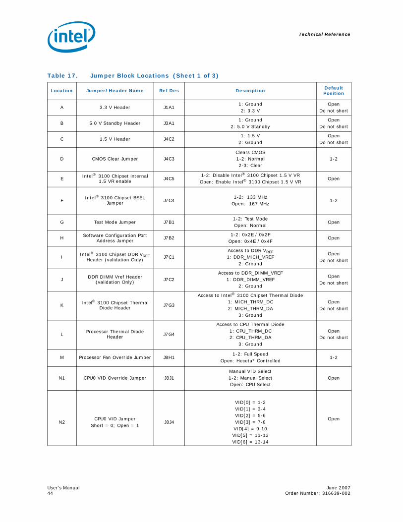
Table 17. Jumper Block Locations (Sheet 1 of 3)
Location Jumper/Header Name Ref Des Description Default Position
A 3.3 V Header J1A11: Ground2: 3.3 V
OpenDo not short
B 5.0 V Standby Header J3A11: Ground
2: 5.0 V StandbyOpen
Do not short
C 1.5 V Header J4C21: 1.5 V
2: GroundOpen
Do not short
D CMOS Clear Jumper J4C3 Clears CMOS1-2: Normal2-3: Clear
1-2
E Intel® 3100 Chipset internal 1.5 VR enable J4C5
1-2: Disable Intel® 3100 Chipset 1.5 V VROpen: Enable Intel® 3100 Chipset 1.5 V VR
Open
F Intel® 3100 Chipset BSEL Jumper J7C4
1-2: 133 MHzOpen: 167 MHz
1-2
G Test Mode Jumper J7B11-2: Test ModeOpen: Normal
Open
H Software Configuration Port Address Jumper J7B2
1-2: 0x2E / 0x2FOpen: 0x4E / 0x4F
Open
I Intel® 3100 Chipset DDR VREF Header (validation Only) J7C1
Access to DDR VREF1: DDR_MICH_VREF
2: Ground
OpenDo not short
J DDR DIMM Vref Header (validation Only) J7C2
Access to DDR_DIMM_VREF1: DDR_DIMM_VREF
2: Ground
OpenDo not short
K Intel® 3100 Chipset Thermal Diode Header J7G3
Access to Intel® 3100 Chipset Thermal Diode1: MICH_THRM_DC2: MICH_THRM_DA
3: Ground
OpenDo not short
L Processor Thermal Diode Header J7G4
Access to CPU Thermal Diode1: CPU_THRM_DC2: CPU_THRM_DA
3: Ground
OpenDo not short
M Processor Fan Override Jumper J8H11-2: Full Speed
Open: Heceta* Controlled1-2
N1 CPU0 VID Override Jumper J8J1Manual VID Select1-2: Manual SelectOpen: CPU Select
Open
N2CPU0 VID Jumper
Short = 0; Open = 1 J8J4
VID[0] = 1-2VID[1] = 3-4VID[2] = 5-6VID[3] = 7-8VID[4] = 9-10VID[5] = 11-12VID[6] = 13-14
Open
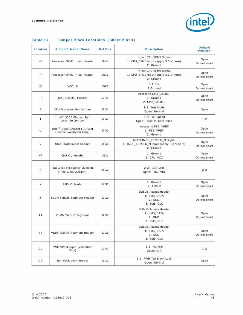
June 2007 User’s ManualOrder Number: 316639-002 45
Technical Reference
O Processor BPM3 Inject Header J9H4Inject CPU BPM3 Signal
1: CPU_BPM0 input (apply 3.3 V here)2: Ground
OpenDo not short
P Processor BPM0 Inject Header J9J1Inject CPU BPM0 Signal
1: CPU_BPM0 input (apply 3.3 V here)2: Ground
OpenDo not short
Q VCC1.8 J9K11.1.8 V
2.GroundOpen
Do not short
R CPU_GTLREF Header J7H2Access to CPU_GTLREF
1: Ground2: CPU_GTLREF
OpenDo not short
S CPU Processor Hot Jumper J8G11-2: Test ModeOpen: Normal
Open
T Intel® 3100 Chipset Fan Override Jumper J7G2
1-2: Full SpeedOpen: Heceta* Controlled
1-2
U Intel® 3100 Chipset FSB Vref Header (validation Only) J7G1
Access to FSB_VREF1: FSB_VREF
2: Ground
OpenDo not short
V Stop Clock Inject Header J4G3Inject IMCH_STPCLK_N Signal
1: IMCH_STPCLK_N input (apply 3.3 V here)2: Ground
OpenDo not short
W CPU VCC Header J5J11: Ground
2: CPU_VCCOpen
Do not short
XFSB Clock Frequency Override
(Host Clock Jumper)J4G2
2-3: 133 MHzOpen: 167 MHz
2-3
Y 1.05 V Header J4G11: Ground2: 1.05 V
OpenDo not short
Z IMCH SMBUS Segment Header J2G3
SMBUS Access Header1: SMB_DATA
2: GND3: SMB_CLK
OpenDo not short
AA DIMM SMBUS Segment J2G7
SMBUS Access Header1: SMB_DATA
2: GND3: SMB_CLK
OpenDo not short
BB VSBY SMBUS Segment Header J2G6
SMBUS Access Header1: SMB_DATA
2: GND3: SMB_CLK
OpenDo not short
CC FWH VPP Jumper (validation Only) J2H2
1-2: NormalOpen: N/A
1-2
DD Top Block Lock Jumper J1G11-2: FWH Top Block Lock
Open: NormalOpen
Table 17. Jumper Block Locations (Sheet 2 of 3)
Location Jumper/Header Name Ref Des Description Default Position
Technical Reference
User’s Manual June 200746 Order Number: 316639-002
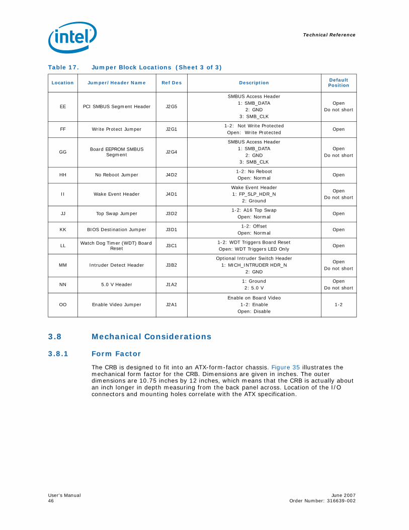
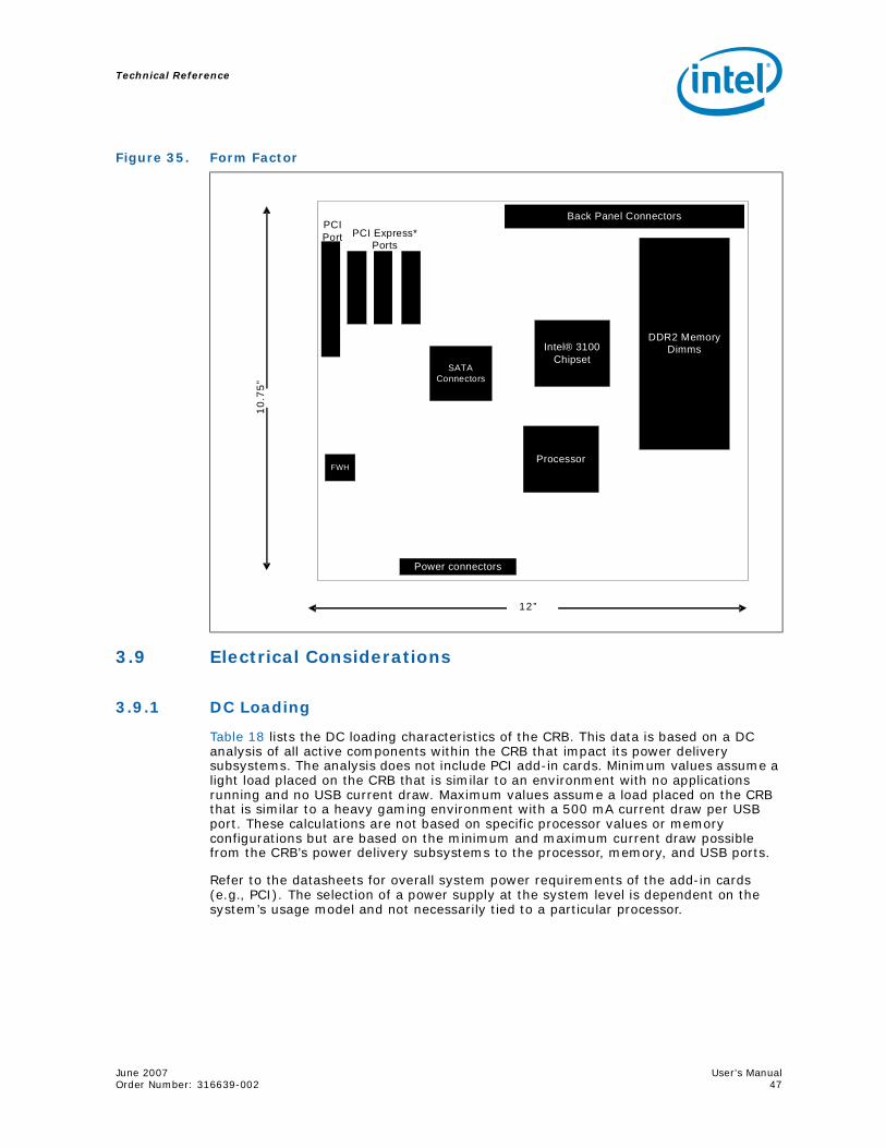
3.8 Mechanical Considerations
3.8.1 Form Factor
The CRB is designed to fit into an ATX-form-factor chassis. Figure 35 illustrates the mechanical form factor for the CRB. Dimensions are given in inches. The outer dimensions are 10.75 inches by 12 inches, which means that the CRB is actually about an inch longer in depth measuring from the back panel across. Location of the I/O connectors and mounting holes correlate with the ATX specification.
EE PCI SMBUS Segment Header J2G5
SMBUS Access Header1: SMB_DATA
2: GND3: SMB_CLK
OpenDo not short
FF Write Protect Jumper J2G11-2: Not Write ProtectedOpen: Write Protected
Open
GG Board EEPROM SMBUS Segment J2G4
SMBUS Access Header1: SMB_DATA
2: GND3: SMB_CLK
OpenDo not short
HH No Reboot Jumper J4D21-2: No RebootOpen: Normal
Open
II Wake Event Header J4D1Wake Event Header1: FP_SLP_HDR_N
2: Ground
OpenDo not short
JJ Top Swap Jumper J3D21-2: A16 Top Swap
Open: NormalOpen
KK BIOS Destination Jumper J3D11-2: Offset
Open: NormalOpen
LL Watch Dog Timer (WDT) Board Reset J3C1
1-2: WDT Triggers Board ResetOpen: WDT Triggers LED Only
Open
MM Intruder Detect Header J3B2Optional Intruder Switch Header
1: MICH_INTRUDER HDR_N2: GND
OpenDo not short
NN 5.0 V Header J1A21: Ground2: 5.0 V
OpenDo not short
OO Enable Video Jumper J2A1Enable on Board Video
1-2: EnableOpen: Disable
1-2
Table 17. Jumper Block Locations (Sheet 3 of 3)
Location Jumper/Header Name Ref Des Description Default Position
June 2007 User’s ManualOrder Number: 316639-002 47
Technical Reference
3.9 Electrical Considerations
3.9.1 DC Loading
Table 18 lists the DC loading characteristics of the CRB. This data is based on a DC analysis of all active components within the CRB that impact its power delivery subsystems. The analysis does not include PCI add-in cards. Minimum values assume a light load placed on the CRB that is similar to an environment with no applications running and no USB current draw. Maximum values assume a load placed on the CRB that is similar to a heavy gaming environment with a 500 mA current draw per USB port. These calculations are not based on specific processor values or memory configurations but are based on the minimum and maximum current draw possible from the CRB’s power delivery subsystems to the processor, memory, and USB ports.
Refer to the datasheets for overall system power requirements of the add-in cards (e.g., PCI). The selection of a power supply at the system level is dependent on the system’s usage model and not necessarily tied to a particular processor.
Figure 35. Form Factor
12”
10.7
5”
DDR2 Memory DimmsIntel® 3100
Chipset
Processor
Back Panel Connectors
Power connectors
SATA Connectors
FWH
PCI Express* Ports
PCI Port
Technical Reference
User’s Manual June 200748 Order Number: 316639-002
3.9.2 Add-in Board Considerations
The CRB is designed to provide 2 A (average) of +5 V current for each add-in board. There is a total of three x4 PCI Express* slots and one PCI 32/33 add-in board.
3.9.3 Fan Connector Current Capability
Warning: The processor fan must be connected to the processor fan connector, not to a chassis fan connector. Connecting the processor fan to a chassis fan connector may result in on-board component damage that will halt fan operation.
3.9.4 Power Supply Considerations
Warning: The +5 V standby line for the power supply must be capable of providing adequate +5 V standby current. Failure to do so can damage the power supply. The total amount of standby current required depends on the wake devices supported and manufacturing options.
The power supply must comply with the following recommendations found in the indicated sections of the ATX form factor specification.
• The voltage relationship between 3.3 VDC and +5 VDC power rails
• The current capability of the +5 VSB line
• All timing parameters
• All voltage tolerances
3.10 Thermal Considerations
This CRB features a thermal protection circuit in the processor voltage regulator area. This circuit protects the processor voltage regulator from overheating and damaging the CRB. Please consult the specific processor datasheet for details about the thermal runoff features supported by the processors paired with the Intel® 3100 Chipset. The triggering temperature level causes the processor to enter a throttling mode (slowing down the processor if it exceeds its maximum operating temperature) and allow the processor voltage regulator to cool down.
Table 18. DC Loading Characteristics Mode
DC Power DC Current at:
+3.3 V +5 V +12 V -12 V +5 VSB
Minimum Loading 300 W 5 A 11 A 19 A 0 A 0.34 A (S0) 1.25 A (S3)
Maximum Loading 500 W 25 A 27 A 36 A 0.40 A 0.34 A (S0) 1.25 A (S3)
Table 19. Fan Connector Current Capability
Fan Connector Maximum Available Current
CPU Fan 3.0 A
Fan 1 3.0 A
Aux Fan 0 3.0 A
Aux Fan 1 3.0 A
June 2007 User’s ManualOrder Number: 316639-002 49
Technical Reference
Note: Use a processor heatsink that provides omni-directional airflow (similar to the type shown in Section 1.8.1.2) to maintain required airflow across the processor voltage regulator area.
Note: When using BIOS Setup program options to increase processor voltage and frequency above the supported ranges, the temperature in the processor voltage regulator area rises. This area of the CRB requires increased airflow. Direct airflow over the processor voltage regulator is crucial to preventing throttling and keeping the processor voltage regulator area cool. This is particularly important when using liquid cooling.
Note: All responsibility for determining the adequacy of any thermal or system design remains solely with the reader. Intel makes no warranties or representations that merely following the instructions presented in this document results in a system with adequate thermal performance.
Overview of BIOS Features
User’s Manual June 200750 Order Number: 316639-002
4.0 Overview of BIOS Features
4.1 Introduction
The BIOS is stored in the Firmware Hub (FWH) and can be updated using a BIOS flash programming tool. The FWH contains the BIOS Setup program, Power On Self Test (POST), the PCI auto-configuration utility, and plug-and-play support.
The BIOS displays a message during POST identifying the type of BIOS and a revision code.
The BIOS Setup program can be used to view and change the BIOS settings for the CRB. The BIOS Setup program is accessed by pressing the <DELETE> key after the POST test and memory test begins and before the operating system begins to boot. The menu bar is shown below.
Table 20 lists the BIOS setup program menu features.
Figure 36. Menu Bar
<MAIN> - <ADVANCED> - <PCIPnP> - <BOOT> - <SECURITY> - <CHIPSET>-<EXIT>
Table 20. BIOS Setup Program Menu Bar
Main ADVANCED PCIPnP BOOT SECURITY CHIPSET EXIT
Displays processor and
memory configurations
Configures advanced
features and settings
Setup for PCI and PCI
Express*
Selects boot options and
configurations
Sets passwords
and security features
Configures different major
components
Saves or discard
changes to setup
program options
Table 21. BIOS Setup Program Function Keys
BIOS Setup Program Function Key Description
< or > Selects a different menu screen (moves the cursor left or right)
^ or ν Selects an item (moves the cursor up or down)
Enter Executes command or selects the submenu
F9 Load the optimal default configuration values for the current menu
F7 Discard changes
F8 Load fail safe defaults
F10 Save the current values and exits the BIOS setup program
ESC Exits the menu
June 2007 User’s ManualOrder Number: 316639-002 51
Overview of BIOS Features
4.2 Resource Configuration
4.2.1 PCI Auto Configuration
The BIOS automatically configures PCI devices. Currently on the CRB there is a 32/33 PCI add-in card socket. Auto configuration lets a user insert or remove PCI cards without having to manually configure the system. When a user turns on the system after adding a PCI card, the BIOS automatically configures interrupts, the I/O space, and other system resources. Any interrupts set to AVAILABLE in Setup are considered to be available for use by add-in card.
4.3 System Management BIOS (SMBIOS)
SMBIOS is a Desktop Management Interface (DMI) compliant method for managing computers in a managed network.
The main component of SMBIOS is the Management Information Format (MIF) database, which contains information about the computing system and its components. Using SMBIOS, a system administrator can obtain the system types, capabilities, operational status, and installation dates for system components. The MIF database defines the data and provides the method for accessing this information. The BIOS enables applications such as third-party management software to use SMBIOS. The BIOS stores and reports the following SMBIOS information:
• BIOS data, such as the BIOS revision level
• Fixed-system data, such as peripherals, serial numbers, and asset tags
• Resource data, such as memory size, cache size, and processor clock frequency
• Dynamic data, such as event detection and error logging
Non-Plug and play operating systems, such as Microsoft Windows NT*, require an additional interface for obtaining the SMBIOS information. The BIOS supports an SMBIOS table interface for such operating systems. Using this support, an SMBIOS service-level application running on a non-Plug and Play operating system can obtain the SMBIOS information.
4.4 Legacy USB Support
Legacy USB support enables USB devices to be used even when the operating system’s USB drivers are not yet available. Legacy USB support is used to access the BIOS Setup program, and to install an operating system that supports USB.
Overview of BIOS Features
User’s Manual June 200752 Order Number: 316639-002
Legacy USB support operates as follows:
1. When you apply power to the computer, legacy support is disabled.
2. POST begins.
3. Legacy USB support is enabled by the BIOS allowing you to use a USB keyboard to enter and configure the BIOS Setup program and the maintenance menu.
4. POST completes.
5. The operating system loads. While the operating system is loading, USB keyboards and mice are recognized and may be used to configure the operating system.
After the operating system loads the USB drivers, all legacy and non-legacy USB devices are recognized by the operating system, and Legacy USB support from the BIOS is no longer used.
To install an operating system that supports USB, follow the operating system’s installation instructions.
4.5 BIOS Updates
The BIOS can be updated using the following tools:
• Using a BIOS burn-in tool (or flash programmer) is the best method to update the BIOS for the CRB. These BIOS updates are available through your FAE. Floppy and USB BIOS Upgrades can also be performed.
Note: Review the instructions distributed with the upgrade utility before attempting a BIOS update.
4.5.1 Language Support
The BIOS Setup program and help messages are supported in US English. Additional languages are available in the Integrator’s Toolkit utility. Check the Intel website for details.
4.6 Boot Options
In the BIOS Setup program, the user can choose to boot from a diskette drive, hard drives, CD-ROM, USB or a network. The default setting is for the Floppy to be the first, and the Hard Drive to be the second.
4.6.1 CD-ROM Boot
Booting from CD-ROM is supported in compliance to the El Torito bootable CD-ROM format specification. Under the Boot menu in the BIOS Setup program, ATAPI CD-ROM is listed as a boot device. Boot devices are defined in priority order. Accordingly, if there is not a bootable CD in the CD-ROM drive, the system attempts to boot from the next defined drive. Refer to Section 4.6.5, “Changing the Boot Device” on page 53 for how to change this setting.
4.6.2 Network Boot
A network can be selected as a boot device provided you have plugged in the PCI Express* Intel gigabit NIC. This selection allows booting from a network add-in card with a remote boot ROM installed.
June 2007 User’s ManualOrder Number: 316639-002 53
Overview of BIOS Features
In order to boot from the LAN, enter the BIOS and select LAN boot as your first boot device. Refer to Section 4.6.5, “Changing the Boot Device” on page 53 for how to change this setting.
4.6.3 USB Boot
• In order to boot from a USB device, Enter BIOS and select USB boot as your first boot device.
Note: Have USB device plugged in when changing this BIOS setting
4.6.4 Booting without Attached Devices
For use in embedded applications, the BIOS has been designed so that after passing the POST, the operating system loader is invoked even if the following devices are not present:
• Video adapter
• Keyboard
• Mouse
4.6.5 Changing the Boot Device
Pressing the <Delete> key during POST causes the BIOS menu to be displayed. Using your arrow keys move over to <BOOT> and then arrow down to <Boot Device Priority> and then select which device you would like to boot first and second.
Note: Please follow the instructions on the right side of the BIOS screen to navigate and change BIOS settings.
4.7 BIOS Security Features
The BIOS includes security features that restrict access to the BIOS Setup program and who can boot the computer. A supervisor password and a user password can be set for the BIOS Setup program and for booting the computer, with the following restrictions:
• The supervisor password gives unrestricted access to view and change all the Setup options in the BIOS Setup program. This is the supervisor mode.
• The user password gives restricted access to view and change Setup options in the BIOS Setup program. This is the user mode.
• If only the supervisor password is set, pressing the <Enter> key at the password prompt of the BIOS Setup program allows the user restricted access to Setup.
• If both the supervisor and user passwords are set, users can enter either the supervisor password or the user password to access Setup. Users have access to Setup respective to which password is entered.
• Setting the user password restricts who can boot the computer. The password prompt is displayed before the computer is booted. If only the supervisor password is set, the computer boots without asking for a password. If both passwords are set, the user can enter either password to boot the computer.
• For enhanced security, use different passwords for the supervisor and user passwords.
• Valid password characters are A-Z, a-z, and 0-9. Passwords may be up to 16 characters in length.
Error Messages and Beep Codes
User’s Manual June 200754 Order Number: 316639-002
5.0 Error Messages and Beep Codes
5.1 Speakers
The CRB-mounted speaker provides audible error message (beep code) information during POST. The location of the on-board speaker is coordinate D4.
5.2 BIOS Beep Codes
Whenever an error occurs during POST, the BIOS exerts and error tone which indicates the problem.
5.3 BIOS Error Messages
Table 23 lists the error messages and provides a brief description of each.
5.4 Port 80h POST Codes
During the POST, the BIOS generates diagnostic progress codes (POST-codes) to I/O port 80h. If the POST fails or execution stops, the last POST code generated by the BIOS is left at port 80h. This code is useful for determining the point where an error occurred.
Table 22. Beep Code Types
Type Pattern Frequency
Memory Error Three long beeps 1280 Hz
Thermal Warning Four alternating beeps: High tone, low tone, high tone, low tone
High tone: 2000 Hz Low tone: 1600 Hz
Table 23. BIOS Error Messages
Error Message Explanation
CMOS Battery Low The battery may be losing power. Replace the battery soon.
CMOS Checksum Bad The CMOS checksum is incorrect. CMOS memory may have been corrupted. Run Setup to reset values.
Memory Size Decreased Memory size has decreased since the last boot. If no memory was removed then memory may be bad.
No Boot Device Available System did not find a device to boot.
June 2007 User’s ManualOrder Number: 316639-002 55
Error Messages and Beep Codes
The following tables provide information about the POST codes generated by the BIOS:
• Table 24 lists the Port 80h POST code ranges
• Table 25 lists the Port 80h POST sequence
Table 24. Port 80h POST Code Ranges
Range (Hex) Category/Subsystem
00 – 0F Debug codes: Can be used by any PEIM/driver for debug.
10 – 1F Host Processors: 1F is an unrecoverable processor error.
20 – 2F Memory/Chipset: 2F is no memory detected or no useful memory detected.
30 – 3F Recovery: 3F indicated recovery failure.
40 – 4F Reserved for future use.
50 – 5F I/O Busses: PCI, USB, ISA, ATA, etc. 5F is an unrecoverable error. Start with PCI.
60 – 6F Reserved for future use (for new busses).
70 – 7F Output Devices: All output consoles. 7F is an unrecoverable error.
80 – 8F Reserved for future use (new output console codes).
90 – 9F Input devices: Keyboard/Mouse. 9F is an unrecoverable error.
A0 – AF Reserved for future use (new input console codes).
B0 – BF Boot Devices: Includes fixed media and removable media. BF is an unrecoverable error.
C0 – CF Reserved for future use.
D0 – DF Boot device selection.
E0 – FF F0 – FF FF processor exception. E0 – EE: Miscellaneous codes. EF boot/S3: resume failure.
Table 25. Typical Port 80h POST Sequence (Sheet 1 of 2)
POST Code Description
21 Initializing a chipset component
22 Reading SPD from memory DIMMs
23 Detecting presence of memory DIMMs
25 Configuring memory
28 Testing memory
34 Loading recovery capsule
E4 Entered DXE phase
12 Starting Application processor initialization
13 SMM initialization
50 Enumerating PCI busses
51 Allocating resources to PCI bus
92 Detecting the presence of the keyboard
90 Resetting keyboard
94 Clearing keyboard input buffer
95 Keyboard Self Test EB Calling Video BIOS
58 Resetting USB bus
Error Messages and Beep Codes
User’s Manual June 200756 Order Number: 316639-002
5A Resetting PATA/SATA bus and all devices
92 Detecting the presence of the keyboard
90 Resetting keyboard
94 Clearing keyboard input buffer
5A Resetting PATA/SATA bus and all devices
28 Testing memory
90 Resetting keyboard
94 Clearing keyboard input buffer
E7 Waiting for user input
01 INT 19
00 Ready to boot
Table 25. Typical Port 80h POST Sequence (Sheet 2 of 2)
POST Code Description