Embed Size (px)
Citation preview

10 General-Purpose Input/Outputs (GPIOs)
The GPIO module is composed of six physical GPIO blocks, each corresponding to an individual
GPIO port (Port A, Port B, Port C, Port D, Port E, Port F). The GPIO module supports up to 43
programmable input/output pins, depending on the peripherals being used.
The GPIO module has the following features:
■ Up to 43 GPIOs, depending on configuration
■ Highly flexible pin muxing allows use as GPIO or one of several peripheral functions
■ 5-V-tolerant in input configuration
■ Ports A-G accessed through the Advanced Peripheral Bus (APB)
■ Fast toggle capable of a change every clock cycle for ports on AHB, every two clock cycles for
ports on APB
■ Programmable control for GPIO interrupts
– Interrupt generation masking
– Edge-triggered on rising, falling, or both
– Level-sensitive on High or Low values
■ Bit masking in both read and write operations through address lines
■ Can be used to initiate an ADC sample sequence or a μDMA transfer
■ Pin state can be retained during Hibernation mode
■ Pins configured as digital inputs are Schmitt-triggered
■ Programmable control for GPIO pad configuration
– Weak pull-up or pull-down resistors
– 2-mA, 4-mA, and 8-mA pad drive for digital communication; up to four pads can sink 18-mA
for high-current applications
– Slew rate control for 8-mA pad drive
– Open drain enables
– Digital input enables
10.1 Signal Description
GPIO signals have alternate hardware functions. The following table lists the GPIO pins and their
analog and digital alternate functions. All GPIO signals are 5-V tolerant when configured as inputs
except for PD4, PD5, PB0 and PB1, which are limited to 3.6 V. The digital alternate hardware functions
are enabled by setting the appropriate bit in the GPIO Alternate Function Select (GPIOAFSEL)
and GPIODEN registers and configuring the PMCx bit field in the GPIO Port Control (GPIOPCTL)
649June 12, 2014
Texas Instruments-Production Data
Tiva™ TM4C123GH6PM Microcontroller

register to the numeric encoding shown in the table below. Analog signals in the table below are
also 5-V tolerant and are configured by clearing the DEN bit in theGPIO Digital Enable (GPIODEN)
register. The AINx analog signals have internal circuitry to protect them from voltages over VDD (up
to the maximum specified in Table 24-1 on page 1358), but analog performance specifications are
only guaranteed if the input signal swing at the I/O pad is kept inside the range 0 V < VIN < VDD.
Note that each pin must be programmed individually; no type of grouping is implied by the columns
in the table. Table entries that are shaded gray are the default values for the corresponding GPIO
pin.
Important: The table below shows special consideration GPIO pins. Most GPIO pins are configured
as GPIOs and tri-stated by default (GPIOAFSEL=0, GPIODEN=0, GPIOPDR=0,
GPIOPUR=0, and GPIOPCTL=0). Special consideration pins may be programed to a
non-GPIO function or may have special commit controls out of reset. In addition, a
Power-On-Reset (POR) or asserting RST returns these GPIO to their original special
consideration state.
Table 10-1. GPIO Pins With Special Considerations
GPIOCRGPIOPCTLGPIOPURGPIOPDRGPIODENGPIOAFSELDefault Reset
State
GPIO Pins
10x10000UART0PA[1:0]
10x20000SSI0PA[5:2]
10x30000I21C0PB[3:2]
00x11011JTAG/SWDPC[3:0]
00x00000GPIOa
PD[7]
00x00000GPIOa
PF[0]
a. This pin is configured as a GPIO by default but is locked and can only be reprogrammed by unlocking the
pin in the GPIOLOCK register and uncommitting it by setting the GPIOCR register.
The GPIO commit control registers provide a layer of protection against accidental
programming of critical hardware signals including the GPIO pins that can function as
JTAG/SWD signals and the NMI signal. The commit control process must be followed
for these pins, even if they are programmed as alternate functions other than JTAG/SWD
or NMI; see “Commit Control” on page 656.
Table 10-2. GPIO Pins and Alternate Functions (64LQFP)
Digital Function (GPIOPCTL PMCx Bit Field Encoding)a
Analog
FunctionPinIO
1514987654321
---CAN1Rx------U0Rx-17PA0
---CAN1Tx------U0Tx-18PA1
---------SSI0Clk--19PA2
---------SSI0Fss--20PA3
---------SSI0Rx--21PA4
---------SSI0Tx--22PA5
------M1PWM2-I2C1SCL---23PA6
------M1PWM3-I2C1SDA---24PA7
----T2CCP0-----U1RxUSB0ID45PB0
June 12, 2014650
Texas Instruments-Production Data
General-Purpose Input/Outputs (GPIOs)

Table 10-2. GPIO Pins and Alternate Functions (64LQFP) (continued)
Digital Function (GPIOPCTL PMCx Bit Field Encoding)a
Analog
FunctionPinIO
1514987654321
----T2CCP1-----U1TxUSB0VBUS46PB1
----T3CCP0---I2C0SCL---47PB2
----T3CCP1---I2C0SDA---48PB3
---CAN0RxT1CCP0--M0PWM2-SSI2Clk-AIN1058PB4
---CAN0TxT1CCP1--M0PWM3-SSI2Fss-AIN1157PB5
----T0CCP0--M0PWM0-SSI2Rx--1PB6
----T0CCP1--M0PWM1-SSI2Tx--4PB7
----T4CCP0-----TCK SWCLK-52PC0
----T4CCP1-----TMS SWDIO-51PC1
----T5CCP0-----TDI-50PC2
----T5CCP1-----TDO SWO-49PC3
---U1RTSWT0CCP0IDX1-M0PWM6-U1RxU4RxC1-16PC4
---U1CTSWT0CCP1PhA1-M0PWM7-U1TxU4TxC1+15PC5
---USB0EPENWT1CCP0PhB1----U3RxC0+14PC6
---USB0PFLTWT1CCP1-----U3TxC0-13PC7
----WT2CCP0-M1PWM0M0PWM6I2C3SCLSSI1ClkSSI3ClkAIN761PD0
----WT2CCP1-M1PWM1M0PWM7I2C3SDASSI1FssSSI3FssAIN662PD1
---USB0EPENWT3CCP0--M0FAULT0-SSI1RxSSI3RxAIN563PD2
---USB0PFLTWT3CCP1IDX0---SSI1TxSSI3TxAIN464PD3
----WT4CCP0-----U6RxUSB0DM43PD4
----WT4CCP1-----U6TxUSB0DP44PD5
----WT5CCP0PhA0-M0FAULT0--U2Rx-53PD6
---NMIWT5CCP1PhB0----U2Tx-10PD7
----------U7RxAIN39PE0
----------U7TxAIN28PE1
-----------AIN17PE2
-----------AIN06PE3
---CAN0Rx--M1PWM2M0PWM4I2C2SCL-U5RxAIN959PE4
---CAN0Tx--M1PWM3M0PWM5I2C2SDA-U5TxAIN860PE5
--C0oNMIT0CCP0PhA0M1PWM4-CAN0RxSSI1RxU1RTS-28PF0
-TRD1C1o-T0CCP1PhB0M1PWM5--SSI1TxU1CTS-29PF1
-TRD0--T1CCP0-M1PWM6M0FAULT0-SSI1Clk--30PF2
-TRCLK--T1CCP1-M1PWM7-CAN0TxSSI1Fss--31PF3
---USB0EPENT2CCP0IDX0M1FAULT0-----5PF4
a. The digital signals that are shaded gray are the power-on default values for the corresponding GPIO pin. Encodings 10-13 are not used
on this device.
651June 12, 2014
Texas Instruments-Production Data
Tiva™ TM4C123GH6PM Microcontroller

10.2 Functional Description
Each GPIO port is a separate hardware instantiation of the same physical block (see Figure
10-1 on page 652 and Figure 10-2 on page 653). The TM4C123GH6PMmicrocontroller contains six
ports and thus six of these physical GPIO blocks. Note that not all pins are implemented on every
block. SomeGPIO pins can function as I/O signals for the on-chip peripheral modules. For information
on which GPIO pins are used for alternate hardware functions, refer to Table 23-5 on page 1351.
Figure 10-1. Digital I/O Pads
Pad
Control
Commit
Control
Data
Control
Interrupt
Control
MUX
MUX
DEMUX
Digital
I/O
Pad
Identification Registers
GPIOPeriphID0
GPIOPeriphID1
GPIOPeriphID2
GPIOPeriphID3
GPIOPeriphID4
GPIOPeriphID5
GPIOPeriphID6
GPIOPeriphID7
GPIOPCellID0
GPIOPCellID1
GPIOPCellID2
GPIOPCellID3
Pad Input
Pad Output
Enable
GPIOLOCK
GPIOCR
GPIODATA
GPIODIR
GPIOISGPIOIBEGPIOIEVGPIOIMGPIORISGPIOMISGPIOICR
GPIODR2RGPIODR4RGPIODR8RGPIOSLRGPIOPURGPIOPDRGPIOODRGPIODEN
Alternate Input
Alternate Output
Alternate Output Enable
Interrupt
GPIO Input
GPIO Output
GPIO Output Enable
Pad OutputPackage I/O Pin
MUX
Periph 0
Periph 1
Periph n
Port
Control
GPIOPCTL
GPIOSI
Mode
Control
GPIOAFSEL
GPIOADCCTL
GPIODMACTL
GPIOAMSEL
June 12, 2014652
Texas Instruments-Production Data
General-Purpose Input/Outputs (GPIOs)

Figure 10-2. Analog/Digital I/O Pads
Pad
Control
Data
ControlGPIO Input
GPIO Output
GPIO Output Enable
Interrupt
Control
InterruptMUX
MUX
GPIODR8R
GPIODR2R
GPIODR4R
GPIOSLR
GPIOPUR
GPIOPDR
GPIOODR
GPIODEN
GPIOAMSEL
GPIOIEV
GPIOIS
GPIOIBE
GPIOIM
GPIORIS
GPIOMIS
GPIOICR
GPIODATA
GPIODIR
Identification Registers
GPIOPeriphID0
GPIOPeriphID1
GPIOPeriphID2
GPIOPeriphID3
GPIOPeriphID4
GPIOPeriphID5
GPIOPeriphID6
GPIOPeriphID7
GPIOPCellID0
GPIOPCellID1
GPIOPCellID2
GPIOPCellID3
Analog Circuitry
(for GPIO pins that
connect to the ADC
input MUX)
ADC
Isolation
Circuit
Pad Output Enable
Package I/O Pin
Pad Input
Pad Output
Analog/Digital
I/O Pad
Commit
Control
GPIOLOCK
GPIOCR
Alternate Input
Alternate Output
Alternate Output Enable
MUX
Periph 0
Periph 1
Periph n
Port
Control
GPIOPCTL
DEMUX
Mode
Control
GPIOAFSEL
GPIOADCCTL
GPIODMACTL
GPIOSI
10.2.1 Data Control
The data control registers allow software to configure the operational modes of the GPIOs. The data
direction register configures the GPIO as an input or an output while the data register either captures
incoming data or drives it out to the pads.
Caution – It is possible to create a software sequence that prevents the debugger from connecting to
the TM4C123GH6PMmicrocontroller. If the program code loaded into flash immediately changes the
JTAG pins to their GPIO functionality, the debugger may not have enough time to connect and halt
the controller before the JTAG pin functionality switches. As a result, the debugger may be locked out
of the part. This issue can be avoided with a software routine that restores JTAG functionality based
on an external or software trigger. In the case that the software routine is not implemented and the
device is locked out of the part, this issue can be solved by using the TM4C123GH6PMFlash Programmer
"Unlock" feature. Please refer to LMFLASHPROGRAMMER on the TI web for more information.
10.2.1.1 Data Direction Operation
The GPIO Direction (GPIODIR) register (see page 663) is used to configure each individual pin as
an input or output. When the data direction bit is cleared, the GPIO is configured as an input, and
the corresponding data register bit captures and stores the value on the GPIO port. When the data
653June 12, 2014
Texas Instruments-Production Data
Tiva™ TM4C123GH6PM Microcontroller

direction bit is set, the GPIO is configured as an output, and the corresponding data register bit is
driven out on the GPIO port.
10.2.1.2 Data Register Operation
To aid in the efficiency of software, the GPIO ports allow for the modification of individual bits in the
GPIO Data (GPIODATA) register (see page 662) by using bits [9:2] of the address bus as a mask.
In this manner, software drivers can modify individual GPIO pins in a single instruction without
affecting the state of the other pins. This method is more efficient than the conventional method of
performing a read-modify-write operation to set or clear an individual GPIO pin. To implement this
feature, the GPIODATA register covers 256 locations in the memory map.
During a write, if the address bit associated with that data bit is set, the value of the GPIODATA
register is altered. If the address bit is cleared, the data bit is left unchanged.
For example, writing a value of 0xEB to the address GPIODATA + 0x098 has the results shown in
Figure 10-3, where u indicates that data is unchanged by the write. This example demonstrates
how GPIODATA bits 5, 2, and 1 are written.
Figure 10-3. GPIODATA Write Example
0 10 0 1 10 0 0
u 1u u 0 1u u
9 8 7 6 5 4 3 2 1 0
1 11 0 0 11 1
7 6 5 4 3 2 1 0
GPIODATA
0xEB
0x098
ADDR[9:2]
0
During a read, if the address bit associated with the data bit is set, the value is read. If the address
bit associated with the data bit is cleared, the data bit is read as a zero, regardless of its actual
value. For example, reading address GPIODATA + 0x0C4 yields as shown in Figure 10-4. This
example shows how to read GPIODATA bits 5, 4, and 0.
Figure 10-4. GPIODATA Read Example
0 10 1 0 00 1 0 0
0 10 1 0 00 0
9 8 7 6 5 4 3 2 1 0
0 11 1 1 11 0
7 6 5 4 3 2 1 0
Returned Value
GPIODATA
0x0C4
ADDR[9:2]
10.2.2 Interrupt Control
The interrupt capabilities of each GPIO port are controlled by a set of seven registers. These registers
are used to select the source of the interrupt, its polarity, and the edge properties. When one or
more GPIO inputs cause an interrupt, a single interrupt output is sent to the interrupt controller for
the entire GPIO port. For edge-triggered interrupts, software must clear the interrupt to enable any
June 12, 2014654
Texas Instruments-Production Data
General-Purpose Input/Outputs (GPIOs)

further interrupts. For a level-sensitive interrupt, the external source must hold the level constant
for the interrupt to be recognized by the controller.
Three registers define the edge or sense that causes interrupts:
■ GPIO Interrupt Sense (GPIOIS) register (see page 664)
■ GPIO Interrupt Both Edges (GPIOIBE) register (see page 665)
■ GPIO Interrupt Event (GPIOIEV) register (see page 666)
Interrupts are enabled/disabled via the GPIO Interrupt Mask (GPIOIM) register (see page 667).
When an interrupt condition occurs, the state of the interrupt signal can be viewed in two locations:
theGPIORaw Interrupt Status (GPIORIS) andGPIOMasked Interrupt Status (GPIOMIS) registers
(see page 668 and page 669). As the name implies, the GPIOMIS register only shows interrupt
conditions that are allowed to be passed to the interrupt controller. The GPIORIS register indicates
that a GPIO pin meets the conditions for an interrupt, but has not necessarily been sent to the
interrupt controller.
For a GPIO level-detect interrupt, the interrupt signal generating the interrupt must be held until
serviced. Once the input signal deasserts from the interrupt generating logical sense, the
corresponding RIS bit in the GPIORIS register clears. For a GPIO edge-detect interrupt, the RIS
bit in the GPIORIS register is cleared by writing a ‘1’ to the corresponding bit in the GPIO Interrupt
Clear (GPIOICR) register (see page 670). The correspondingGPIOMIS bit reflects the masked value
of the RIS bit.
When programming the interrupt control registers (GPIOIS, GPIOIBE, or GPIOIEV), the interrupts
should be masked (GPIOIM cleared). Writing any value to an interrupt control register can generate
a spurious interrupt if the corresponding bits are enabled.
10.2.2.1 ADC Trigger Source
Any GPIO pin can be configured to be an external trigger for the ADC using theGPIO ADC Control
(GPIOADCCTL) register. If any GPIO is configured as a non-masked interrupt pin (the appropriate
bit of GPIOIM is set), and an interrupt for that port is generated, a trigger signal is sent to the ADC.
If the ADC Event Multiplexer Select (ADCEMUX) register is configured to use the external trigger,
an ADC conversion is initiated. See page 833.
Note that if the Port BGPIOADCCTL register is cleared, PB4 can still be used as an external trigger
for the ADC. This is a legacy mode which allows code written for previous devices to operate on
this microcontroller.
10.2.2.2 μDMA Trigger Source
Any GPIO pin can be configured to be an external trigger for the μDMA using theGPIODMAControl
(GPIODMACTL) register. If any GPIO is configured as a non-masked interrupt pin (the appropriate
bit of GPIOIM is set), an interrupt for that port is generated and an external trigger signal is sent to
the μDMA. If the μDMA is configured to start a transfer based on the GPIO signal, a transfer is
initiated.
10.2.3 Mode Control
The GPIO pins can be controlled by either software or hardware. Software control is the default for
most signals and corresponds to the GPIO mode, where the GPIODATA register is used to read
or write the corresponding pins. When hardware control is enabled via theGPIO Alternate Function
655June 12, 2014
Texas Instruments-Production Data
Tiva™ TM4C123GH6PM Microcontroller

Select (GPIOAFSEL) register (see page 671), the pin state is controlled by its alternate function
(that is, the peripheral).
Further pin muxing options are provided through theGPIO Port Control (GPIOPCTL) register which
selects one of several peripheral functions for each GPIO. For information on the configuration
options, refer to Table 23-5 on page 1351.
Note: If any pin is to be used as an ADC input, the appropriate bit in the GPIOAMSEL register
must be set to disable the analog isolation circuit.
10.2.4 Commit Control
The GPIO commit control registers provide a layer of protection against accidental programming of
critical hardware peripherals. Protection is provided for the GPIO pins that can be used as the four
JTAG/SWD pins and the NMI pin (see “Signal Tables” on page 1329 for pin numbers). Writes to
protected bits of theGPIO Alternate Function Select (GPIOAFSEL) register (see page 671),GPIO
Pull Up Select (GPIOPUR) register (see page 677), GPIO Pull-Down Select (GPIOPDR) register
(see page 679), andGPIO Digital Enable (GPIODEN) register (see page 682) are not committed to
storage unless the GPIO Lock (GPIOLOCK) register (see page 684) has been unlocked and the
appropriate bits of the GPIO Commit (GPIOCR) register (see page 685) have been set.
10.2.5 Pad Control
The pad control registers allow software to configure the GPIO pads based on the application
requirements. The pad control registers include theGPIODR2R,GPIODR4R,GPIODR8R,GPIOODR,
GPIOPUR, GPIOPDR, GPIOSLR, and GPIODEN registers. These registers control drive strength,
open-drain configuration, pull-up and pull-down resistors, slew-rate control and digital input enable
for each GPIO. If 5 V is applied to a GPIO configured as an open-drain output, the output voltage
will depend on the strength of your pull-up resistor. The GPIO pad is not electrically configured to
output 5 V.
10.2.6 Identification
The identification registers configured at reset allow software to detect and identify the module as
a GPIO block. The identification registers include theGPIOPeriphID0-GPIOPeriphID7 registers as
well as the GPIOPCellID0-GPIOPCellID3 registers.
10.3 Initialization and Configuration
The GPIO modules may be accessed via two different memory apertures. The legacy aperture, the
Advanced Peripheral Bus (APB), is backwards-compatible with previous devices. The other aperture,
the Advanced High-Performance Bus (AHB), offers the same register map but provides better
back-to-back access performance than the APB bus. These apertures are mutually exclusive. The
aperture enabled for a given GPIO port is controlled by the appropriate bit in the GPIOHBCTL
register (see page 258). Note that GPIO can only be accessed through the AHB aperture.
To configure the GPIO pins of a particular port, follow these steps:
1. Enable the clock to the port by setting the appropriate bits in the RCGCGPIO register (see
page 340). In addition, the SCGCGPIO and DCGCGPIO registers can be programmed in the
same manner to enable clocking in Sleep and Deep-Sleep modes.
2. Set the direction of the GPIO port pins by programming the GPIODIR register. A write of a 1
indicates output and a write of a 0 indicates input.
June 12, 2014656
Texas Instruments-Production Data
General-Purpose Input/Outputs (GPIOs)

3. Configure theGPIOAFSEL register to program each bit as a GPIO or alternate pin. If an alternate
pin is chosen for a bit, then the PMCx field must be programmed in the GPIOPCTL register for
the specific peripheral required. There are also two registers,GPIOADCCTL andGPIODMACTL,
which can be used to program a GPIO pin as a ADC or μDMA trigger, respectively.
4. Set the drive strength for each of the pins through theGPIODR2R,GPIODR4R, andGPIODR8R
registers.
5. Program each pad in the port to have either pull-up, pull-down, or open drain functionality through
the GPIOPUR, GPIOPDR, GPIOODR register. Slew rate may also be programmed, if needed,
through the GPIOSLR register.
6. To enable GPIO pins as digital I/Os, set the appropriate DEN bit in the GPIODEN register. To
enable GPIO pins to their analog function (if available), set the GPIOAMSEL bit in the
GPIOAMSEL register.
7. Program the GPIOIS, GPIOIBE, GPIOEV, and GPIOIM registers to configure the type, event,
and mask of the interrupts for each port.
Note: To prevent false interrupts, the following steps should be taken when re-configuring
GPIO edge and interrupt sense registers:
a. Mask the corresponding port by clearing the IME field in the GPIOIM register.
b. Configure the IS field in the GPIOIS register and the IBE field in the GPIOIBE
register.
c. Clear the GPIORIS register.
d. Unmask the port by setting the IME field in the GPIOIM register.
8. Optionally, software can lock the configurations of the NMI and JTAG/SWD pins on the GPIO
port pins, by setting the LOCK bits in the GPIOLOCK register.
When the internal POR signal is asserted and until otherwise configured, all GPIO pins are configured
to be undriven (tristate): GPIOAFSEL=0, GPIODEN=0, GPIOPDR=0, and GPIOPUR=0, except for
the pins shown in Table 10-1 on page 650. Table 10-3 on page 657 shows all possible configurations
of the GPIO pads and the control register settings required to achieve them. Table 10-4 on page 658
shows how a rising edge interrupt is configured for pin 2 of a GPIO port.
Table 10-3. GPIO Pad Configuration Examples
GPIO Register Bit Valuea
ConfigurationSLRDR8RDR4RDR2RPDRPURDENODRDIRAFSEL
XXXX??1000Digital Input (GPIO)
??????1010Digital Output (GPIO)
????XX1110Open Drain Output
(GPIO)
????XX11X1Open Drain
Input/Output (I2CSDA)
????XX10X1Digital Input/Output
(I2CSCL)
XXXX??10X1Digital Input (Timer
CCP)
657June 12, 2014
Texas Instruments-Production Data
Tiva™ TM4C123GH6PM Microcontroller

Table 10-3. GPIO Pad Configuration Examples (continued)
GPIO Register Bit Valuea
ConfigurationSLRDR8RDR4RDR2RPDRPURDENODRDIRAFSEL
XXXX??10X1Digital Input (QEI)
??????10X1Digital Output (PWM)
??????10X1Digital Output (Timer
PWM)
??????10X1Digital Input/Output
(SSI)
??????10X1Digital Input/Output
(UART)
XXXX000000Analog Input
(Comparator)
??????10X1Digital Output
(Comparator)
a. X=Ignored (don’t care bit)
?=Can be either 0 or 1, depending on the configuration
Table 10-4. GPIO Interrupt Configuration Example
Pin 2 Bit Valuea
Desired Interrupt
Event TriggerRegister
01234567
XX0XXXXX0=edge
1=level
GPIOIS
XX0XXXXX0=single edge
1=both edges
GPIOIBE
XX1XXXXX0=Low level, or falling
edge
1=High level, or rising
edge
GPIOIEV
001000000=masked
1=not masked
GPIOIM
a. X=Ignored (don’t care bit)
10.4 Register Map
Table 10-6 on page 660 lists the GPIO registers. Each GPIO port can be accessed through one of
two bus apertures. The legacy aperture, the Advanced Peripheral Bus (APB), is backwards-compatible
with previous devices. The other aperture, the Advanced High-Performance Bus (AHB), offers the
same register map but provides better back-to-back access performance than the APB bus.
Important: The GPIO registers in this chapter are duplicated in each GPIO block; however,
depending on the block, all eight bits may not be connected to a GPIO pad. In those
cases, writing to unconnected bits has no effect, and reading unconnected bits returns
no meaningful data. See “Signal Description” on page 649 for the GPIOs included on
this device.
The offset listed is a hexadecimal increment to the register's address, relative to that GPIO port's
base address:
■ GPIO Port A (APB): 0x4000.4000
June 12, 2014658
Texas Instruments-Production Data
General-Purpose Input/Outputs (GPIOs)

■ GPIO Port A (AHB): 0x4005.8000
■ GPIO Port B (APB): 0x4000.5000
■ GPIO Port B (AHB): 0x4005.9000
■ GPIO Port C (APB): 0x4000.6000
■ GPIO Port C (AHB): 0x4005.A000
■ GPIO Port D (APB): 0x4000.7000
■ GPIO Port D (AHB): 0x4005.B000
■ GPIO Port E (APB): 0x4002.4000
■ GPIO Port E (AHB): 0x4005.C000
■ GPIO Port F (APB): 0x4002.5000
■ GPIO Port F (AHB): 0x4005.D000
Note that each GPIO module clock must be enabled before the registers can be programmed (see
page 340). There must be a delay of 3 system clocks after the GPIOmodule clock is enabled before
any GPIO module registers are accessed.
Important: The table below shows special consideration GPIO pins. Most GPIO pins are configured
as GPIOs and tri-stated by default (GPIOAFSEL=0, GPIODEN=0, GPIOPDR=0,
GPIOPUR=0, and GPIOPCTL=0). Special consideration pins may be programed to a
non-GPIO function or may have special commit controls out of reset. In addition, a
Power-On-Reset (POR) or asserting RST returns these GPIO to their original special
consideration state.
Table 10-5. GPIO Pins With Special Considerations
GPIOCRGPIOPCTLGPIOPURGPIOPDRGPIODENGPIOAFSELDefault Reset
State
GPIO Pins
10x10000UART0PA[1:0]
10x20000SSI0PA[5:2]
10x30000I21C0PB[3:2]
00x11011JTAG/SWDPC[3:0]
00x00000GPIOa
PD[7]
00x00000GPIOa
PF[0]
a. This pin is configured as a GPIO by default but is locked and can only be reprogrammed by unlocking the
pin in the GPIOLOCK register and uncommitting it by setting the GPIOCR register.
The GPIO commit control registers provide a layer of protection against accidental
programming of critical hardware signals including the GPIO pins that can function as
JTAG/SWD signals and the NMI signal. The commit control process must be followed
for these pins, even if they are programmed as alternate functions other than JTAG/SWD
or NMI; see “Commit Control” on page 656.
The default register type for the GPIOCR register is RO for all GPIO pins with the exception of the
NMI pin and the four JTAG/SWD pins (see “Signal Tables” on page 1329 for pin numbers). These six
pins are the only GPIOs that are protected by the GPIOCR register. Because of this, the register
type for the corresponding GPIO Ports is RW.
The default reset value for theGPIOCR register is 0x0000.00FF for all GPIO pins, with the exception
of the NMI and JTAG/SWD pins (see “Signal Tables” on page 1329 for pin numbers). To ensure that
the JTAG and NMI pins are not accidentally programmed as GPIO pins, these pins default to
non-committable. Because of this, the default reset value ofGPIOCR changes for the corresponding
ports.
659June 12, 2014
Texas Instruments-Production Data
Tiva™ TM4C123GH6PM Microcontroller

Table 10-6. GPIO Register Map
See
pageDescriptionResetTypeNameOffset
662GPIO Data0x0000.0000RWGPIODATA0x000
663GPIO Direction0x0000.0000RWGPIODIR0x400
664GPIO Interrupt Sense0x0000.0000RWGPIOIS0x404
665GPIO Interrupt Both Edges0x0000.0000RWGPIOIBE0x408
666GPIO Interrupt Event0x0000.0000RWGPIOIEV0x40C
667GPIO Interrupt Mask0x0000.0000RWGPIOIM0x410
668GPIO Raw Interrupt Status0x0000.0000ROGPIORIS0x414
669GPIO Masked Interrupt Status0x0000.0000ROGPIOMIS0x418
670GPIO Interrupt Clear0x0000.0000W1CGPIOICR0x41C
671GPIO Alternate Function Select-RWGPIOAFSEL0x420
673GPIO 2-mA Drive Select0x0000.00FFRWGPIODR2R0x500
674GPIO 4-mA Drive Select0x0000.0000RWGPIODR4R0x504
675GPIO 8-mA Drive Select0x0000.0000RWGPIODR8R0x508
676GPIO Open Drain Select0x0000.0000RWGPIOODR0x50C
677GPIO Pull-Up Select-RWGPIOPUR0x510
679GPIO Pull-Down Select0x0000.0000RWGPIOPDR0x514
681GPIO Slew Rate Control Select0x0000.0000RWGPIOSLR0x518
682GPIO Digital Enable-RWGPIODEN0x51C
684GPIO Lock0x0000.0001RWGPIOLOCK0x520
685GPIO Commit--GPIOCR0x524
687GPIO Analog Mode Select0x0000.0000RWGPIOAMSEL0x528
688GPIO Port Control-RWGPIOPCTL0x52C
690GPIO ADC Control0x0000.0000RWGPIOADCCTL0x530
691GPIO DMA Control0x0000.0000RWGPIODMACTL0x534
692GPIO Peripheral Identification 40x0000.0000ROGPIOPeriphID40xFD0
693GPIO Peripheral Identification 50x0000.0000ROGPIOPeriphID50xFD4
694GPIO Peripheral Identification 60x0000.0000ROGPIOPeriphID60xFD8
695GPIO Peripheral Identification 70x0000.0000ROGPIOPeriphID70xFDC
696GPIO Peripheral Identification 00x0000.0061ROGPIOPeriphID00xFE0
697GPIO Peripheral Identification 10x0000.0000ROGPIOPeriphID10xFE4
698GPIO Peripheral Identification 20x0000.0018ROGPIOPeriphID20xFE8
699GPIO Peripheral Identification 30x0000.0001ROGPIOPeriphID30xFEC
June 12, 2014660
Texas Instruments-Production Data
General-Purpose Input/Outputs (GPIOs)

Table 10-6. GPIO Register Map (continued)
See
pageDescriptionResetTypeNameOffset
700GPIO PrimeCell Identification 00x0000.000DROGPIOPCellID00xFF0
701GPIO PrimeCell Identification 10x0000.00F0ROGPIOPCellID10xFF4
702GPIO PrimeCell Identification 20x0000.0005ROGPIOPCellID20xFF8
703GPIO PrimeCell Identification 30x0000.00B1ROGPIOPCellID30xFFC
10.5 Register Descriptions
The remainder of this section lists and describes the GPIO registers, in numerical order by address
offset.
661June 12, 2014
Texas Instruments-Production Data
Tiva™ TM4C123GH6PM Microcontroller
Register 1: GPIO Data (GPIODATA), offset 0x000
The GPIODATA register is the data register. In software control mode, values written in the
GPIODATA register are transferred onto the GPIO port pins if the respective pins have been
configured as outputs through the GPIO Direction (GPIODIR) register (see page 663).
In order to write to GPIODATA, the corresponding bits in the mask, resulting from the address bus
bits [9:2], must be set. Otherwise, the bit values remain unchanged by the write.
Similarly, the values read from this register are determined for each bit by the mask bit derived from
the address used to access the data register, bits [9:2]. Bits that are set in the address mask cause
the corresponding bits in GPIODATA to be read, and bits that are clear in the address mask cause
the corresponding bits in GPIODATA to be read as 0, regardless of their value.
A read from GPIODATA returns the last bit value written if the respective pins are configured as
outputs, or it returns the value on the corresponding input pin when these are configured as inputs.
All bits are cleared by a reset.
GPIO Data (GPIODATA)
GPIO Port A (APB) base: 0x4000.4000GPIO Port A (AHB) base: 0x4005.8000GPIO Port B (APB) base: 0x4000.5000GPIO Port B (AHB) base: 0x4005.9000GPIO Port C (APB) base: 0x4000.6000GPIO Port C (AHB) base: 0x4005.A000GPIO Port D (APB) base: 0x4000.7000GPIO Port D (AHB) base: 0x4005.B000GPIO Port E (APB) base: 0x4002.4000GPIO Port E (AHB) base: 0x4005.C000GPIO Port F (APB) base: 0x4002.5000GPIO Port F (AHB) base: 0x4005.D000Offset 0x000Type RW, reset 0x0000.0000
16171819202122232425262728293031
reserved
ROROROROROROROROROROROROROROROROType
0000000000000000Reset
0123456789101112131415
DATAreserved
RWRWRWRWRWRWRWRWROROROROROROROROType
0000000000000000Reset
DescriptionResetTypeNameBit/Field
Software should not rely on the value of a reserved bit. To provide
compatibility with future products, the value of a reserved bit should be
preserved across a read-modify-write operation.
0x0000.00ROreserved31:8
GPIO Data
This register is virtually mapped to 256 locations in the address space.
To facilitate the reading and writing of data to these registers by
independent drivers, the data read from and written to the registers are
masked by the eight address lines [9:2]. Reads from this register return
its current state. Writes to this register only affect bits that are not masked
by ADDR[9:2] and are configured as outputs. See “Data Register
Operation” on page 654 for examples of reads and writes.
0x00RWDATA7:0
June 12, 2014662
Texas Instruments-Production Data
General-Purpose Input/Outputs (GPIOs)

Register 2: GPIO Direction (GPIODIR), offset 0x400
TheGPIODIR register is the data direction register. Setting a bit in theGPIODIR register configures
the corresponding pin to be an output, while clearing a bit configures the corresponding pin to be
an input. All bits are cleared by a reset, meaning all GPIO pins are inputs by default.
GPIO Direction (GPIODIR)
GPIO Port A (APB) base: 0x4000.4000GPIO Port A (AHB) base: 0x4005.8000GPIO Port B (APB) base: 0x4000.5000GPIO Port B (AHB) base: 0x4005.9000GPIO Port C (APB) base: 0x4000.6000GPIO Port C (AHB) base: 0x4005.A000GPIO Port D (APB) base: 0x4000.7000GPIO Port D (AHB) base: 0x4005.B000GPIO Port E (APB) base: 0x4002.4000GPIO Port E (AHB) base: 0x4005.C000GPIO Port F (APB) base: 0x4002.5000GPIO Port F (AHB) base: 0x4005.D000Offset 0x400Type RW, reset 0x0000.0000
16171819202122232425262728293031
reserved
ROROROROROROROROROROROROROROROROType
0000000000000000Reset
0123456789101112131415
DIRreserved
RWRWRWRWRWRWRWRWROROROROROROROROType
0000000000000000Reset
DescriptionResetTypeNameBit/Field
Software should not rely on the value of a reserved bit. To provide
compatibility with future products, the value of a reserved bit should be
preserved across a read-modify-write operation.
0x0000.00ROreserved31:8
GPIO Data Direction
DescriptionValue
Corresponding pin is an input.0
Corresponding pins is an output.1
0x00RWDIR7:0
663June 12, 2014
Texas Instruments-Production Data
Tiva™ TM4C123GH6PM Microcontroller

Register 3: GPIO Interrupt Sense (GPIOIS), offset 0x404
The GPIOIS register is the interrupt sense register. Setting a bit in the GPIOIS register configures
the corresponding pin to detect levels, while clearing a bit configures the corresponding pin to detect
edges. All bits are cleared by a reset.
Note: To prevent false interrupts, the following steps should be taken when re-configuring GPIO
edge and interrupt sense registers:
1. Mask the corresponding port by clearing the IME field in the GPIOIM register.
2. Configure the IS field in the GPIOIS register and the IBE field in the GPIOIBE register.
3. Clear the GPIORIS register.
4. Unmask the port by setting the IME field in the GPIOIM register.
GPIO Interrupt Sense (GPIOIS)
GPIO Port A (APB) base: 0x4000.4000GPIO Port A (AHB) base: 0x4005.8000GPIO Port B (APB) base: 0x4000.5000GPIO Port B (AHB) base: 0x4005.9000GPIO Port C (APB) base: 0x4000.6000GPIO Port C (AHB) base: 0x4005.A000GPIO Port D (APB) base: 0x4000.7000GPIO Port D (AHB) base: 0x4005.B000GPIO Port E (APB) base: 0x4002.4000GPIO Port E (AHB) base: 0x4005.C000GPIO Port F (APB) base: 0x4002.5000GPIO Port F (AHB) base: 0x4005.D000Offset 0x404Type RW, reset 0x0000.0000
16171819202122232425262728293031
reserved
ROROROROROROROROROROROROROROROROType
0000000000000000Reset
0123456789101112131415
ISreserved
RWRWRWRWRWRWRWRWROROROROROROROROType
0000000000000000Reset
DescriptionResetTypeNameBit/Field
Software should not rely on the value of a reserved bit. To provide
compatibility with future products, the value of a reserved bit should be
preserved across a read-modify-write operation.
0x0000.00ROreserved31:8
GPIO Interrupt Sense
DescriptionValue
The edge on the corresponding pin is detected (edge-sensitive).0
The level on the corresponding pin is detected (level-sensitive).1
0x00RWIS7:0
June 12, 2014664
Texas Instruments-Production Data
General-Purpose Input/Outputs (GPIOs)

Register 4: GPIO Interrupt Both Edges (GPIOIBE), offset 0x408
The GPIOIBE register allows both edges to cause interrupts. When the corresponding bit in the
GPIO Interrupt Sense (GPIOIS) register (see page 664) is set to detect edges, setting a bit in the
GPIOIBE register configures the corresponding pin to detect both rising and falling edges, regardless
of the corresponding bit in the GPIO Interrupt Event (GPIOIEV) register (see page 666). Clearing
a bit configures the pin to be controlled by the GPIOIEV register. All bits are cleared by a reset.
Note: To prevent false interrupts, the following steps should be taken when re-configuring GPIO
edge and interrupt sense registers:
1. Mask the corresponding port by clearing the IME field in the GPIOIM register.
2. Configure the IS field in the GPIOIS register and the IBE field in the GPIOIBE register.
3. Clear the GPIORIS register.
4. Unmask the port by setting the IME field in the GPIOIM register.
GPIO Interrupt Both Edges (GPIOIBE)
GPIO Port A (APB) base: 0x4000.4000GPIO Port A (AHB) base: 0x4005.8000GPIO Port B (APB) base: 0x4000.5000GPIO Port B (AHB) base: 0x4005.9000GPIO Port C (APB) base: 0x4000.6000GPIO Port C (AHB) base: 0x4005.A000GPIO Port D (APB) base: 0x4000.7000GPIO Port D (AHB) base: 0x4005.B000GPIO Port E (APB) base: 0x4002.4000GPIO Port E (AHB) base: 0x4005.C000GPIO Port F (APB) base: 0x4002.5000GPIO Port F (AHB) base: 0x4005.D000Offset 0x408Type RW, reset 0x0000.0000
16171819202122232425262728293031
reserved
ROROROROROROROROROROROROROROROROType
0000000000000000Reset
0123456789101112131415
IBEreserved
RWRWRWRWRWRWRWRWROROROROROROROROType
0000000000000000Reset
DescriptionResetTypeNameBit/Field
Software should not rely on the value of a reserved bit. To provide
compatibility with future products, the value of a reserved bit should be
preserved across a read-modify-write operation.
0x0000.00ROreserved31:8
GPIO Interrupt Both Edges
DescriptionValue
Interrupt generation is controlled by the GPIO Interrupt Event
(GPIOIEV) register (see page 666).
0
Both edges on the corresponding pin trigger an interrupt.1
0x00RWIBE7:0
665June 12, 2014
Texas Instruments-Production Data
Tiva™ TM4C123GH6PM Microcontroller

Register 5: GPIO Interrupt Event (GPIOIEV), offset 0x40C
TheGPIOIEV register is the interrupt event register. Setting a bit in theGPIOIEV register configures
the corresponding pin to detect rising edges or high levels, depending on the corresponding bit
value in the GPIO Interrupt Sense (GPIOIS) register (see page 664). Clearing a bit configures the
pin to detect falling edges or low levels, depending on the corresponding bit value in the GPIOIS
register. All bits are cleared by a reset.
GPIO Interrupt Event (GPIOIEV)
GPIO Port A (APB) base: 0x4000.4000GPIO Port A (AHB) base: 0x4005.8000GPIO Port B (APB) base: 0x4000.5000GPIO Port B (AHB) base: 0x4005.9000GPIO Port C (APB) base: 0x4000.6000GPIO Port C (AHB) base: 0x4005.A000GPIO Port D (APB) base: 0x4000.7000GPIO Port D (AHB) base: 0x4005.B000GPIO Port E (APB) base: 0x4002.4000GPIO Port E (AHB) base: 0x4005.C000GPIO Port F (APB) base: 0x4002.5000GPIO Port F (AHB) base: 0x4005.D000Offset 0x40CType RW, reset 0x0000.0000
16171819202122232425262728293031
reserved
ROROROROROROROROROROROROROROROROType
0000000000000000Reset
0123456789101112131415
IEVreserved
RWRWRWRWRWRWRWRWROROROROROROROROType
0000000000000000Reset
DescriptionResetTypeNameBit/Field
Software should not rely on the value of a reserved bit. To provide
compatibility with future products, the value of a reserved bit should be
preserved across a read-modify-write operation.
0x0000.00ROreserved31:8
GPIO Interrupt Event
DescriptionValue
A falling edge or a Low level on the corresponding pin triggers
an interrupt.
0
A rising edge or a High level on the corresponding pin triggers
an interrupt.
1
0x00RWIEV7:0
June 12, 2014666
Texas Instruments-Production Data
General-Purpose Input/Outputs (GPIOs)

Register 6: GPIO Interrupt Mask (GPIOIM), offset 0x410
The GPIOIM register is the interrupt mask register. Setting a bit in the GPIOIM register allows
interrupts that are generated by the corresponding pin to be sent to the interrupt controller on the
combined interrupt signal. Clearing a bit prevents an interrupt on the corresponding pin from being
sent to the interrupt controller. All bits are cleared by a reset.
GPIO Interrupt Mask (GPIOIM)
GPIO Port A (APB) base: 0x4000.4000GPIO Port A (AHB) base: 0x4005.8000GPIO Port B (APB) base: 0x4000.5000GPIO Port B (AHB) base: 0x4005.9000GPIO Port C (APB) base: 0x4000.6000GPIO Port C (AHB) base: 0x4005.A000GPIO Port D (APB) base: 0x4000.7000GPIO Port D (AHB) base: 0x4005.B000GPIO Port E (APB) base: 0x4002.4000GPIO Port E (AHB) base: 0x4005.C000GPIO Port F (APB) base: 0x4002.5000GPIO Port F (AHB) base: 0x4005.D000Offset 0x410Type RW, reset 0x0000.0000
16171819202122232425262728293031
reserved
ROROROROROROROROROROROROROROROROType
0000000000000000Reset
0123456789101112131415
IMEreserved
RWRWRWRWRWRWRWRWROROROROROROROROType
0000000000000000Reset
DescriptionResetTypeNameBit/Field
Software should not rely on the value of a reserved bit. To provide
compatibility with future products, the value of a reserved bit should be
preserved across a read-modify-write operation.
0ROreserved31:8
GPIO Interrupt Mask Enable
DescriptionValue
The interrupt from the corresponding pin is masked.0
The interrupt from the corresponding pin is sent to the interrupt
controller.
1
0x00RWIME7:0
667June 12, 2014
Texas Instruments-Production Data
Tiva™ TM4C123GH6PM Microcontroller

Register 7: GPIO Raw Interrupt Status (GPIORIS), offset 0x414
TheGPIORIS register is the raw interrupt status register. A bit in this register is set when an interrupt
condition occurs on the corresponding GPIO pin. If the corresponding bit in the GPIO Interrupt
Mask (GPIOIM) register (see page 667) is set, the interrupt is sent to the interrupt controller. Bits
read as zero indicate that corresponding input pins have not initiated an interrupt. For a GPIO
level-detect interrupt, the interrupt signal generating the interrupt must be held until serviced. Once
the input signal deasserts from the interrupt generating logical sense, the corresponding RIS bit in
the GPIORIS register clears. For a GPIO edge-detect interrupt, the RIS bit in the GPIORIS register
is cleared by writing a ‘1’ to the corresponding bit in the GPIO Interrupt Clear (GPIOICR) register.
The corresponding GPIOMIS bit reflects the masked value of the RIS bit.
GPIO Raw Interrupt Status (GPIORIS)
GPIO Port A (APB) base: 0x4000.4000GPIO Port A (AHB) base: 0x4005.8000GPIO Port B (APB) base: 0x4000.5000GPIO Port B (AHB) base: 0x4005.9000GPIO Port C (APB) base: 0x4000.6000GPIO Port C (AHB) base: 0x4005.A000GPIO Port D (APB) base: 0x4000.7000GPIO Port D (AHB) base: 0x4005.B000GPIO Port E (APB) base: 0x4002.4000GPIO Port E (AHB) base: 0x4005.C000GPIO Port F (APB) base: 0x4002.5000GPIO Port F (AHB) base: 0x4005.D000Offset 0x414Type RO, reset 0x0000.0000
16171819202122232425262728293031
reserved
ROROROROROROROROROROROROROROROROType
0000000000000000Reset
0123456789101112131415
RISreserved
ROROROROROROROROROROROROROROROROType
0000000000000000Reset
DescriptionResetTypeNameBit/Field
Software should not rely on the value of a reserved bit. To provide
compatibility with future products, the value of a reserved bit should be
preserved across a read-modify-write operation.
0ROreserved31:8
GPIO Interrupt Raw Status
DescriptionValue
An interrupt condition has not occurred on the corresponding
pin.
0
An interrupt condition has occurred on the corresponding pin.1
For edge-detect interrupts, this bit is cleared by writing a 1 to the
corresponding bit in the GPIOICR register.
For a GPIO level-detect interrupt, the bit is cleared when the level is
deasserted.
0x00RORIS7:0
June 12, 2014668
Texas Instruments-Production Data
General-Purpose Input/Outputs (GPIOs)
Register 8: GPIO Masked Interrupt Status (GPIOMIS), offset 0x418
The GPIOMIS register is the masked interrupt status register. If a bit is set in this register, the
corresponding interrupt has triggered an interrupt to the interrupt controller. If a bit is clear, either
no interrupt has been generated, or the interrupt is masked.
Note that if the Port BGPIOADCCTL register is cleared, PB4 can still be used as an external trigger
for the ADC. This is a legacy mode which allows code written for previous devices to operate on
this microcontroller.
GPIOMIS is the state of the interrupt after masking.
GPIO Masked Interrupt Status (GPIOMIS)
GPIO Port A (APB) base: 0x4000.4000GPIO Port A (AHB) base: 0x4005.8000GPIO Port B (APB) base: 0x4000.5000GPIO Port B (AHB) base: 0x4005.9000GPIO Port C (APB) base: 0x4000.6000GPIO Port C (AHB) base: 0x4005.A000GPIO Port D (APB) base: 0x4000.7000GPIO Port D (AHB) base: 0x4005.B000GPIO Port E (APB) base: 0x4002.4000GPIO Port E (AHB) base: 0x4005.C000GPIO Port F (APB) base: 0x4002.5000GPIO Port F (AHB) base: 0x4005.D000Offset 0x418Type RO, reset 0x0000.0000
16171819202122232425262728293031
reserved
ROROROROROROROROROROROROROROROROType
0000000000000000Reset
0123456789101112131415
MISreserved
ROROROROROROROROROROROROROROROROType
0000000000000000Reset
DescriptionResetTypeNameBit/Field
Software should not rely on the value of a reserved bit. To provide
compatibility with future products, the value of a reserved bit should be
preserved across a read-modify-write operation.
0ROreserved31:8
GPIO Masked Interrupt Status
DescriptionValue
An interrupt condition on the corresponding pin is masked or
has not occurred.
0
An interrupt condition on the corresponding pin has triggered
an interrupt to the interrupt controller.
1
For edge-detect interrupts, this bit is cleared by writing a 1 to the
corresponding bit in the GPIOICR register.
For a GPIO level-detect interrupt, the bit is cleared when the level is
deasserted.
0x00ROMIS7:0
669June 12, 2014
Texas Instruments-Production Data
Tiva™ TM4C123GH6PM Microcontroller

Register 9: GPIO Interrupt Clear (GPIOICR), offset 0x41C
The GPIOICR register is the interrupt clear register. For edge-detect interrupts, writing a 1 to the
IC bit in theGPIOICR register clears the corresponding bit in theGPIORIS andGPIOMIS registers.
If the interrupt is a level-detect, the IC bit in this register has no effect. In addition, writing a 0 to any
of the bits in the GPIOICR register has no effect.
GPIO Interrupt Clear (GPIOICR)
GPIO Port A (APB) base: 0x4000.4000GPIO Port A (AHB) base: 0x4005.8000GPIO Port B (APB) base: 0x4000.5000GPIO Port B (AHB) base: 0x4005.9000GPIO Port C (APB) base: 0x4000.6000GPIO Port C (AHB) base: 0x4005.A000GPIO Port D (APB) base: 0x4000.7000GPIO Port D (AHB) base: 0x4005.B000GPIO Port E (APB) base: 0x4002.4000GPIO Port E (AHB) base: 0x4005.C000GPIO Port F (APB) base: 0x4002.5000GPIO Port F (AHB) base: 0x4005.D000Offset 0x41CType W1C, reset 0x0000.0000
16171819202122232425262728293031
reserved
ROROROROROROROROROROROROROROROROType
0000000000000000Reset
0123456789101112131415
ICreserved
W1CW1CW1CW1CW1CW1CW1CW1CROROROROROROROROType
0000000000000000Reset
DescriptionResetTypeNameBit/Field
Software should not rely on the value of a reserved bit. To provide
compatibility with future products, the value of a reserved bit should be
preserved across a read-modify-write operation.
0ROreserved31:8
GPIO Interrupt Clear
DescriptionValue
The corresponding interrupt is unaffected.0
The corresponding interrupt is cleared.1
0x00W1CIC7:0
June 12, 2014670
Texas Instruments-Production Data
General-Purpose Input/Outputs (GPIOs)

Register 10: GPIO Alternate Function Select (GPIOAFSEL), offset 0x420
The GPIOAFSEL register is the mode control select register. If a bit is clear, the pin is used as a
GPIO and is controlled by the GPIO registers. Setting a bit in this register configures the
corresponding GPIO line to be controlled by an associated peripheral. Several possible peripheral
functions are multiplexed on each GPIO. The GPIO Port Control (GPIOPCTL) register is used to
select one of the possible functions. Table 23-5 on page 1351 details which functions are muxed on
each GPIO pin. The reset value for this register is 0x0000.0000 for GPIO ports that are not listed
in the table below.
Important: The table below shows special consideration GPIO pins. Most GPIO pins are configured
as GPIOs and tri-stated by default (GPIOAFSEL=0, GPIODEN=0, GPIOPDR=0,
GPIOPUR=0, and GPIOPCTL=0). Special consideration pins may be programed to a
non-GPIO function or may have special commit controls out of reset. In addition, a
Power-On-Reset (POR) or asserting RST returns these GPIO to their original special
consideration state.
Table 10-7. GPIO Pins With Special Considerations
GPIOCRGPIOPCTLGPIOPURGPIOPDRGPIODENGPIOAFSELDefault Reset
State
GPIO Pins
10x10000UART0PA[1:0]
10x20000SSI0PA[5:2]
10x30000I21C0PB[3:2]
00x11011JTAG/SWDPC[3:0]
00x00000GPIOa
PD[7]
00x00000GPIOa
PF[0]
a. This pin is configured as a GPIO by default but is locked and can only be reprogrammed by unlocking the
pin in the GPIOLOCK register and uncommitting it by setting the GPIOCR register.
The GPIO commit control registers provide a layer of protection against accidental
programming of critical hardware signals including the GPIO pins that can function as
JTAG/SWD signals and the NMI signal. The commit control process must be followed
for these pins, even if they are programmed as alternate functions other than JTAG/SWD
or NMI; see “Commit Control” on page 656.
Caution – It is possible to create a software sequence that prevents the debugger from connecting to
the TM4C123GH6PMmicrocontroller. If the program code loaded into flash immediately changes the
JTAG pins to their GPIO functionality, the debugger may not have enough time to connect and halt
the controller before the JTAG pin functionality switches. As a result, the debugger may be locked out
of the part. This issue can be avoided with a software routine that restores JTAG functionality based
on an external or software trigger. In the case that the software routine is not implemented and the
device is locked out of the part, this issue can be solved by using the TM4C123GH6PMFlash Programmer
"Unlock" feature. Please refer to LMFLASHPROGRAMMER on the TI web for more information.
The GPIO commit control registers provide a layer of protection against accidental programming of
critical hardware peripherals. Protection is provided for the GPIO pins that can be used as the four
JTAG/SWD pins and the NMI pin (see “Signal Tables” on page 1329 for pin numbers). Writes to
protected bits of theGPIO Alternate Function Select (GPIOAFSEL) register (see page 671),GPIO
Pull Up Select (GPIOPUR) register (see page 677), GPIO Pull-Down Select (GPIOPDR) register
(see page 679), andGPIO Digital Enable (GPIODEN) register (see page 682) are not committed to
storage unless the GPIO Lock (GPIOLOCK) register (see page 684) has been unlocked and the
appropriate bits of the GPIO Commit (GPIOCR) register (see page 685) have been set.
671June 12, 2014
Texas Instruments-Production Data
Tiva™ TM4C123GH6PM Microcontroller

When using the I2C module, in addition to setting the GPIOAFSEL register bits for the I2C clock
and data pins, the data pins should be set to open drain using the GPIO Open Drain Select
(GPIOODR) register (see examples in “Initialization and Configuration” on page 656).
GPIO Alternate Function Select (GPIOAFSEL)
GPIO Port A (APB) base: 0x4000.4000GPIO Port A (AHB) base: 0x4005.8000GPIO Port B (APB) base: 0x4000.5000GPIO Port B (AHB) base: 0x4005.9000GPIO Port C (APB) base: 0x4000.6000GPIO Port C (AHB) base: 0x4005.A000GPIO Port D (APB) base: 0x4000.7000GPIO Port D (AHB) base: 0x4005.B000GPIO Port E (APB) base: 0x4002.4000GPIO Port E (AHB) base: 0x4005.C000GPIO Port F (APB) base: 0x4002.5000GPIO Port F (AHB) base: 0x4005.D000Offset 0x420Type RW, reset -
16171819202122232425262728293031
reserved
ROROROROROROROROROROROROROROROROType
0000000000000000Reset
0123456789101112131415
AFSELreserved
RWRWRWRWRWRWRWRWROROROROROROROROType
--------00000000Reset
DescriptionResetTypeNameBit/Field
Software should not rely on the value of a reserved bit. To provide
compatibility with future products, the value of a reserved bit should be
preserved across a read-modify-write operation.
0x0000.00ROreserved31:8
GPIO Alternate Function Select
DescriptionValue
The associated pin functions as a GPIO and is controlled by
the GPIO registers.
0
The associated pin functions as a peripheral signal and is
controlled by the alternate hardware function.
The reset value for this register is 0x0000.0000 for GPIO ports
that are not listed in Table 10-1 on page 650.
1
-RWAFSEL7:0
June 12, 2014672
Texas Instruments-Production Data
General-Purpose Input/Outputs (GPIOs)

Register 11: GPIO 2-mA Drive Select (GPIODR2R), offset 0x500
The GPIODR2R register is the 2-mA drive control register. Each GPIO signal in the port can be
individually configured without affecting the other pads. When setting the DRV2 bit for a GPIO signal,
the corresponding DRV4 bit in the GPIODR4R register and DRV8 bit in the GPIODR8R register are
automatically cleared by hardware. By default, all GPIO pins have 2-mA drive.
GPIO 2-mA Drive Select (GPIODR2R)
GPIO Port A (APB) base: 0x4000.4000GPIO Port A (AHB) base: 0x4005.8000GPIO Port B (APB) base: 0x4000.5000GPIO Port B (AHB) base: 0x4005.9000GPIO Port C (APB) base: 0x4000.6000GPIO Port C (AHB) base: 0x4005.A000GPIO Port D (APB) base: 0x4000.7000GPIO Port D (AHB) base: 0x4005.B000GPIO Port E (APB) base: 0x4002.4000GPIO Port E (AHB) base: 0x4005.C000GPIO Port F (APB) base: 0x4002.5000GPIO Port F (AHB) base: 0x4005.D000Offset 0x500Type RW, reset 0x0000.00FF
16171819202122232425262728293031
reserved
ROROROROROROROROROROROROROROROROType
0000000000000000Reset
0123456789101112131415
DRV2reserved
RWRWRWRWRWRWRWRWROROROROROROROROType
1111111100000000Reset
DescriptionResetTypeNameBit/Field
Software should not rely on the value of a reserved bit. To provide
compatibility with future products, the value of a reserved bit should be
preserved across a read-modify-write operation.
0x0000.00ROreserved31:8
Output Pad 2-mA Drive Enable
DescriptionValue
The drive for the corresponding GPIO pin is controlled by the
GPIODR4R or GPIODR8R register.
0
The corresponding GPIO pin has 2-mA drive.1
Setting a bit in either the GPIODR4 register or the GPIODR8 register
clears the corresponding 2-mA enable bit. The change is effective on
the second clock cycle after the write if accessing GPIO via the APB
memory aperture. If using AHB access, the change is effective on the
next clock cycle.
0xFFRWDRV27:0
673June 12, 2014
Texas Instruments-Production Data
Tiva™ TM4C123GH6PM Microcontroller

Register 12: GPIO 4-mA Drive Select (GPIODR4R), offset 0x504
The GPIODR4R register is the 4-mA drive control register. Each GPIO signal in the port can be
individually configured without affecting the other pads. When setting the DRV4 bit for a GPIO signal,
the corresponding DRV2 bit in the GPIODR2R register and DRV8 bit in the GPIODR8R register are
automatically cleared by hardware.
GPIO 4-mA Drive Select (GPIODR4R)
GPIO Port A (APB) base: 0x4000.4000GPIO Port A (AHB) base: 0x4005.8000GPIO Port B (APB) base: 0x4000.5000GPIO Port B (AHB) base: 0x4005.9000GPIO Port C (APB) base: 0x4000.6000GPIO Port C (AHB) base: 0x4005.A000GPIO Port D (APB) base: 0x4000.7000GPIO Port D (AHB) base: 0x4005.B000GPIO Port E (APB) base: 0x4002.4000GPIO Port E (AHB) base: 0x4005.C000GPIO Port F (APB) base: 0x4002.5000GPIO Port F (AHB) base: 0x4005.D000Offset 0x504Type RW, reset 0x0000.0000
16171819202122232425262728293031
reserved
ROROROROROROROROROROROROROROROROType
0000000000000000Reset
0123456789101112131415
DRV4reserved
RWRWRWRWRWRWRWRWROROROROROROROROType
0000000000000000Reset
DescriptionResetTypeNameBit/Field
Software should not rely on the value of a reserved bit. To provide
compatibility with future products, the value of a reserved bit should be
preserved across a read-modify-write operation.
0x0000.00ROreserved31:8
Output Pad 4-mA Drive Enable
DescriptionValue
The drive for the corresponding GPIO pin is controlled by the
GPIODR2R or GPIODR8R register.
0
The corresponding GPIO pin has 4-mA drive.1
Setting a bit in either the GPIODR2 register or the GPIODR8 register
clears the corresponding 4-mA enable bit. The change is effective on
the second clock cycle after the write if accessing GPIO via the APB
memory aperture. If using AHB access, the change is effective on the
next clock cycle.
0x00RWDRV47:0
June 12, 2014674
Texas Instruments-Production Data
General-Purpose Input/Outputs (GPIOs)
Register 13: GPIO 8-mA Drive Select (GPIODR8R), offset 0x508
The GPIODR8R register is the 8-mA drive control register. Each GPIO signal in the port can be
individually configured without affecting the other pads. When setting the DRV8 bit for a GPIO signal,
the corresponding DRV2 bit in the GPIODR2R register and DRV4 bit in the GPIODR4R register are
automatically cleared by hardware. The 8-mA setting is also used for high-current operation.
Note: There is no configuration difference between 8-mA and high-current operation. The additional
current capacity results from a shift in the VOH/VOL levels. See “Recommended Operating
Conditions” on page 1360 for further information.
GPIO 8-mA Drive Select (GPIODR8R)
GPIO Port A (APB) base: 0x4000.4000GPIO Port A (AHB) base: 0x4005.8000GPIO Port B (APB) base: 0x4000.5000GPIO Port B (AHB) base: 0x4005.9000GPIO Port C (APB) base: 0x4000.6000GPIO Port C (AHB) base: 0x4005.A000GPIO Port D (APB) base: 0x4000.7000GPIO Port D (AHB) base: 0x4005.B000GPIO Port E (APB) base: 0x4002.4000GPIO Port E (AHB) base: 0x4005.C000GPIO Port F (APB) base: 0x4002.5000GPIO Port F (AHB) base: 0x4005.D000Offset 0x508Type RW, reset 0x0000.0000
16171819202122232425262728293031
reserved
ROROROROROROROROROROROROROROROROType
0000000000000000Reset
0123456789101112131415
DRV8reserved
RWRWRWRWRWRWRWRWROROROROROROROROType
0000000000000000Reset
DescriptionResetTypeNameBit/Field
Software should not rely on the value of a reserved bit. To provide
compatibility with future products, the value of a reserved bit should be
preserved across a read-modify-write operation.
0x0000.00ROreserved31:8
Output Pad 8-mA Drive Enable
DescriptionValue
The drive for the corresponding GPIO pin is controlled by the
GPIODR2R or GPIODR4R register.
0
The corresponding GPIO pin has 8-mA drive.1
Setting a bit in either the GPIODR2 register or the GPIODR4 register
clears the corresponding 8-mA enable bit. The change is effective on
the second clock cycle after the write if accessing GPIO via the APB
memory aperture. If using AHB access, the change is effective on the
next clock cycle.
0x00RWDRV87:0
675June 12, 2014
Texas Instruments-Production Data
Tiva™ TM4C123GH6PM Microcontroller

Register 14: GPIO Open Drain Select (GPIOODR), offset 0x50C
The GPIOODR register is the open drain control register. Setting a bit in this register enables the
open-drain configuration of the corresponding GPIO pad. When open-drain mode is enabled, the
corresponding bit should also be set in theGPIODigital Enable (GPIODEN) register (see page 682).
Corresponding bits in the drive strength and slew rate control registers (GPIODR2R, GPIODR4R,
GPIODR8R, andGPIOSLR) can be set to achieve the desired fall times. The GPIO acts as an input
if the corresponding bit in the GPIODIR register is cleared. If open drain is selected while the GPIO
is configured as an input, the GPIO will remain an input and the open-drain selection has no effect
until the GPIO is changed to an output.
When using the I2Cmodule, in addition to configuring the data pin to open drain, theGPIO Alternate
Function Select (GPIOAFSEL) register bits for the I2C clock and data pins should be set (see
examples in “Initialization and Configuration” on page 656).
GPIO Open Drain Select (GPIOODR)
GPIO Port A (APB) base: 0x4000.4000GPIO Port A (AHB) base: 0x4005.8000GPIO Port B (APB) base: 0x4000.5000GPIO Port B (AHB) base: 0x4005.9000GPIO Port C (APB) base: 0x4000.6000GPIO Port C (AHB) base: 0x4005.A000GPIO Port D (APB) base: 0x4000.7000GPIO Port D (AHB) base: 0x4005.B000GPIO Port E (APB) base: 0x4002.4000GPIO Port E (AHB) base: 0x4005.C000GPIO Port F (APB) base: 0x4002.5000GPIO Port F (AHB) base: 0x4005.D000Offset 0x50CType RW, reset 0x0000.0000
16171819202122232425262728293031
reserved
ROROROROROROROROROROROROROROROROType
0000000000000000Reset
0123456789101112131415
ODEreserved
RWRWRWRWRWRWRWRWROROROROROROROROType
0000000000000000Reset
DescriptionResetTypeNameBit/Field
Software should not rely on the value of a reserved bit. To provide
compatibility with future products, the value of a reserved bit should be
preserved across a read-modify-write operation.
0x0000.00ROreserved31:8
Output Pad Open Drain Enable
DescriptionValue
The corresponding pin is not configured as open drain.0
The corresponding pin is configured as open drain.1
0x00RWODE7:0
June 12, 2014676
Texas Instruments-Production Data
General-Purpose Input/Outputs (GPIOs)

Register 15: GPIO Pull-Up Select (GPIOPUR), offset 0x510
The GPIOPUR register is the pull-up control register. When a bit is set, a weak pull-up resistor on
the corresponding GPIO signal is enabled. Setting a bit in GPIOPUR automatically clears the
corresponding bit in theGPIO Pull-Down Select (GPIOPDR) register (see page 679). Write access
to this register is protected with theGPIOCR register. Bits inGPIOCR that are cleared prevent writes
to the equivalent bit in this register.
Important: The table below shows special consideration GPIO pins. Most GPIO pins are configured
as GPIOs and tri-stated by default (GPIOAFSEL=0, GPIODEN=0, GPIOPDR=0,
GPIOPUR=0, and GPIOPCTL=0). Special consideration pins may be programed to a
non-GPIO function or may have special commit controls out of reset. In addition, a
Power-On-Reset (POR) or asserting RST returns these GPIO to their original special
consideration state.
Table 10-8. GPIO Pins With Special Considerations
GPIOCRGPIOPCTLGPIOPURGPIOPDRGPIODENGPIOAFSELDefault Reset
State
GPIO Pins
10x10000UART0PA[1:0]
10x20000SSI0PA[5:2]
10x30000I21C0PB[3:2]
00x11011JTAG/SWDPC[3:0]
00x00000GPIOa
PD[7]
00x00000GPIOa
PF[0]
a. This pin is configured as a GPIO by default but is locked and can only be reprogrammed by unlocking the
pin in the GPIOLOCK register and uncommitting it by setting the GPIOCR register.
The GPIO commit control registers provide a layer of protection against accidental
programming of critical hardware signals including the GPIO pins that can function as
JTAG/SWD signals and the NMI signal. The commit control process must be followed
for these pins, even if they are programmed as alternate functions other than JTAG/SWD
or NMI; see “Commit Control” on page 656.
Note: The GPIO commit control registers provide a layer of protection against accidental
programming of critical hardware peripherals. Protection is provided for the GPIO pins that
can be used as the four JTAG/SWD pins and the NMI pin (see “Signal Tables” on page 1329
for pin numbers). Writes to protected bits of the GPIO Alternate Function Select
(GPIOAFSEL) register (see page 671), GPIO Pull Up Select (GPIOPUR) register (see
page 677),GPIO Pull-Down Select (GPIOPDR) register (see page 679), andGPIO Digital
Enable (GPIODEN) register (see page 682) are not committed to storage unless the GPIO
Lock (GPIOLOCK) register (see page 684) has been unlocked and the appropriate bits of
the GPIO Commit (GPIOCR) register (see page 685) have been set.
677June 12, 2014
Texas Instruments-Production Data
Tiva™ TM4C123GH6PM Microcontroller

GPIO Pull-Up Select (GPIOPUR)
GPIO Port A (APB) base: 0x4000.4000GPIO Port A (AHB) base: 0x4005.8000GPIO Port B (APB) base: 0x4000.5000GPIO Port B (AHB) base: 0x4005.9000GPIO Port C (APB) base: 0x4000.6000GPIO Port C (AHB) base: 0x4005.A000GPIO Port D (APB) base: 0x4000.7000GPIO Port D (AHB) base: 0x4005.B000GPIO Port E (APB) base: 0x4002.4000GPIO Port E (AHB) base: 0x4005.C000GPIO Port F (APB) base: 0x4002.5000GPIO Port F (AHB) base: 0x4005.D000Offset 0x510Type RW, reset -
16171819202122232425262728293031
reserved
ROROROROROROROROROROROROROROROROType
0000000000000000Reset
0123456789101112131415
PUEreserved
RWRWRWRWRWRWRWRWROROROROROROROROType
--------00000000Reset
DescriptionResetTypeNameBit/Field
Software should not rely on the value of a reserved bit. To provide
compatibility with future products, the value of a reserved bit should be
preserved across a read-modify-write operation.
0x0000.00ROreserved31:8
Pad Weak Pull-Up Enable
DescriptionValue
The corresponding pin's weak pull-up resistor is disabled.0
The corresponding pin's weak pull-up resistor is enabled.1
Setting a bit in the GPIOPDR register clears the corresponding bit in
the GPIOPUR register. The change is effective on the second clock
cycle after the write if accessing GPIO via the APB memory aperture.
If using AHB access, the change is effective on the next clock cycle.
The reset value for this register is 0x0000.0000 for GPIO ports that are
not listed in Table 10-1 on page 650.
-RWPUE7:0
June 12, 2014678
Texas Instruments-Production Data
General-Purpose Input/Outputs (GPIOs)

Register 16: GPIO Pull-Down Select (GPIOPDR), offset 0x514
TheGPIOPDR register is the pull-down control register. When a bit is set, a weak pull-down resistor
on the corresponding GPIO signal is enabled. Setting a bit in GPIOPDR automatically clears the
corresponding bit in the GPIO Pull-Up Select (GPIOPUR) register (see page 677).
Important: The table below shows special consideration GPIO pins. Most GPIO pins are configured
as GPIOs and tri-stated by default (GPIOAFSEL=0, GPIODEN=0, GPIOPDR=0,
GPIOPUR=0, and GPIOPCTL=0). Special consideration pins may be programed to a
non-GPIO function or may have special commit controls out of reset. In addition, a
Power-On-Reset (POR) or asserting RST returns these GPIO to their original special
consideration state.
Table 10-9. GPIO Pins With Special Considerations
GPIOCRGPIOPCTLGPIOPURGPIOPDRGPIODENGPIOAFSELDefault Reset
State
GPIO Pins
10x10000UART0PA[1:0]
10x20000SSI0PA[5:2]
10x30000I21C0PB[3:2]
00x11011JTAG/SWDPC[3:0]
00x00000GPIOa
PD[7]
00x00000GPIOa
PF[0]
a. This pin is configured as a GPIO by default but is locked and can only be reprogrammed by unlocking the
pin in the GPIOLOCK register and uncommitting it by setting the GPIOCR register.
The GPIO commit control registers provide a layer of protection against accidental
programming of critical hardware signals including the GPIO pins that can function as
JTAG/SWD signals and the NMI signal. The commit control process must be followed
for these pins, even if they are programmed as alternate functions other than JTAG/SWD
or NMI; see “Commit Control” on page 656.
Note: The GPIO commit control registers provide a layer of protection against accidental
programming of critical hardware peripherals. Protection is provided for the GPIO pins that
can be used as the four JTAG/SWD pins and the NMI pin (see “Signal Tables” on page 1329
for pin numbers). Writes to protected bits of the GPIO Alternate Function Select
(GPIOAFSEL) register (see page 671), GPIO Pull Up Select (GPIOPUR) register (see
page 677),GPIO Pull-Down Select (GPIOPDR) register (see page 679), andGPIO Digital
Enable (GPIODEN) register (see page 682) are not committed to storage unless the GPIO
Lock (GPIOLOCK) register (see page 684) has been unlocked and the appropriate bits of
the GPIO Commit (GPIOCR) register (see page 685) have been set.
679June 12, 2014
Texas Instruments-Production Data
Tiva™ TM4C123GH6PM Microcontroller

GPIO Pull-Down Select (GPIOPDR)
GPIO Port A (APB) base: 0x4000.4000GPIO Port A (AHB) base: 0x4005.8000GPIO Port B (APB) base: 0x4000.5000GPIO Port B (AHB) base: 0x4005.9000GPIO Port C (APB) base: 0x4000.6000GPIO Port C (AHB) base: 0x4005.A000GPIO Port D (APB) base: 0x4000.7000GPIO Port D (AHB) base: 0x4005.B000GPIO Port E (APB) base: 0x4002.4000GPIO Port E (AHB) base: 0x4005.C000GPIO Port F (APB) base: 0x4002.5000GPIO Port F (AHB) base: 0x4005.D000Offset 0x514Type RW, reset 0x0000.0000
16171819202122232425262728293031
reserved
ROROROROROROROROROROROROROROROROType
0000000000000000Reset
0123456789101112131415
PDEreserved
RWRWRWRWRWRWRWRWROROROROROROROROType
0000000000000000Reset
DescriptionResetTypeNameBit/Field
Software should not rely on the value of a reserved bit. To provide
compatibility with future products, the value of a reserved bit should be
preserved across a read-modify-write operation.
0x0000.00ROreserved31:8
Pad Weak Pull-Down Enable
DescriptionValue
The corresponding pin's weak pull-down resistor is disabled.0
The corresponding pin's weak pull-down resistor is enabled.1
Setting a bit in the GPIOPUR register clears the corresponding bit in
the GPIOPDR register. The change is effective on the second clock
cycle after the write if accessing GPIO via the APB memory aperture.
If using AHB access, the change is effective on the next clock cycle.
0x00RWPDE7:0
June 12, 2014680
Texas Instruments-Production Data
General-Purpose Input/Outputs (GPIOs)

Register 17: GPIO Slew Rate Control Select (GPIOSLR), offset 0x518
The GPIOSLR register is the slew rate control register. Slew rate control is only available when
using the 8-mA drive strength option. The selection of drive strength is done through theGPIO 8-mA
Drive Select (GPIODR8R) register.
GPIO Slew Rate Control Select (GPIOSLR)
GPIO Port A (APB) base: 0x4000.4000GPIO Port A (AHB) base: 0x4005.8000GPIO Port B (APB) base: 0x4000.5000GPIO Port B (AHB) base: 0x4005.9000GPIO Port C (APB) base: 0x4000.6000GPIO Port C (AHB) base: 0x4005.A000GPIO Port D (APB) base: 0x4000.7000GPIO Port D (AHB) base: 0x4005.B000GPIO Port E (APB) base: 0x4002.4000GPIO Port E (AHB) base: 0x4005.C000GPIO Port F (APB) base: 0x4002.5000GPIO Port F (AHB) base: 0x4005.D000Offset 0x518Type RW, reset 0x0000.0000
16171819202122232425262728293031
reserved
ROROROROROROROROROROROROROROROROType
0000000000000000Reset
0123456789101112131415
SRLreserved
RWRWRWRWRWRWRWRWROROROROROROROROType
0000000000000000Reset
DescriptionResetTypeNameBit/Field
Software should not rely on the value of a reserved bit. To provide
compatibility with future products, the value of a reserved bit should be
preserved across a read-modify-write operation.
0x0000.00ROreserved31:8
Slew Rate Limit Enable (8-mA drive only)
DescriptionValue
Slew rate control is disabled for the corresponding pin.0
Slew rate control is enabled for the corresponding pin.1
0x00RWSRL7:0
681June 12, 2014
Texas Instruments-Production Data
Tiva™ TM4C123GH6PM Microcontroller

Register 18: GPIO Digital Enable (GPIODEN), offset 0x51C
Note: Pins configured as digital inputs are Schmitt-triggered.
TheGPIODEN register is the digital enable register. By default, all GPIO signals except those listed
below are configured out of reset to be undriven (tristate). Their digital function is disabled; they do
not drive a logic value on the pin and they do not allow the pin voltage into the GPIO receiver. To
use the pin as a digital input or output (either GPIO or alternate function), the corresponding GPIODEN
bit must be set.
Important: The table below shows special consideration GPIO pins. Most GPIO pins are configured
as GPIOs and tri-stated by default (GPIOAFSEL=0, GPIODEN=0, GPIOPDR=0,
GPIOPUR=0, and GPIOPCTL=0). Special consideration pins may be programed to a
non-GPIO function or may have special commit controls out of reset. In addition, a
Power-On-Reset (POR) or asserting RST returns these GPIO to their original special
consideration state.
Table 10-10. GPIO Pins With Special Considerations
GPIOCRGPIOPCTLGPIOPURGPIOPDRGPIODENGPIOAFSELDefault Reset
State
GPIO Pins
10x10000UART0PA[1:0]
10x20000SSI0PA[5:2]
10x30000I21C0PB[3:2]
00x11011JTAG/SWDPC[3:0]
00x00000GPIOa
PD[7]
00x00000GPIOa
PF[0]
a. This pin is configured as a GPIO by default but is locked and can only be reprogrammed by unlocking the
pin in the GPIOLOCK register and uncommitting it by setting the GPIOCR register.
The GPIO commit control registers provide a layer of protection against accidental
programming of critical hardware signals including the GPIO pins that can function as
JTAG/SWD signals and the NMI signal. The commit control process must be followed
for these pins, even if they are programmed as alternate functions other than JTAG/SWD
or NMI; see “Commit Control” on page 656.
Note: The GPIO commit control registers provide a layer of protection against accidental
programming of critical hardware peripherals. Protection is provided for the GPIO pins that
can be used as the four JTAG/SWD pins and the NMI pin (see “Signal Tables” on page 1329
for pin numbers). Writes to protected bits of the GPIO Alternate Function Select
(GPIOAFSEL) register (see page 671), GPIO Pull Up Select (GPIOPUR) register (see
page 677),GPIO Pull-Down Select (GPIOPDR) register (see page 679), andGPIO Digital
Enable (GPIODEN) register (see page 682) are not committed to storage unless the GPIO
Lock (GPIOLOCK) register (see page 684) has been unlocked and the appropriate bits of
the GPIO Commit (GPIOCR) register (see page 685) have been set.
June 12, 2014682
Texas Instruments-Production Data
General-Purpose Input/Outputs (GPIOs)

GPIO Digital Enable (GPIODEN)
GPIO Port A (APB) base: 0x4000.4000GPIO Port A (AHB) base: 0x4005.8000GPIO Port B (APB) base: 0x4000.5000GPIO Port B (AHB) base: 0x4005.9000GPIO Port C (APB) base: 0x4000.6000GPIO Port C (AHB) base: 0x4005.A000GPIO Port D (APB) base: 0x4000.7000GPIO Port D (AHB) base: 0x4005.B000GPIO Port E (APB) base: 0x4002.4000GPIO Port E (AHB) base: 0x4005.C000GPIO Port F (APB) base: 0x4002.5000GPIO Port F (AHB) base: 0x4005.D000Offset 0x51CType RW, reset -
16171819202122232425262728293031
reserved
ROROROROROROROROROROROROROROROROType
0000000000000000Reset
0123456789101112131415
DENreserved
RWRWRWRWRWRWRWRWROROROROROROROROType
--------00000000Reset
DescriptionResetTypeNameBit/Field
Software should not rely on the value of a reserved bit. To provide
compatibility with future products, the value of a reserved bit should be
preserved across a read-modify-write operation.
0x0000.00ROreserved31:8
Digital Enable
DescriptionValue
The digital functions for the corresponding pin are disabled.0
The digital functions for the corresponding pin are enabled.
The reset value for this register is 0x0000.0000 for GPIO ports
that are not listed in Table 10-1 on page 650.
1
-RWDEN7:0
683June 12, 2014
Texas Instruments-Production Data
Tiva™ TM4C123GH6PM Microcontroller

Register 19: GPIO Lock (GPIOLOCK), offset 0x520
The GPIOLOCK register enables write access to the GPIOCR register (see page 685). Writing
0x4C4F.434B to the GPIOLOCK register unlocks the GPIOCR register. Writing any other value to
the GPIOLOCK register re-enables the locked state. Reading the GPIOLOCK register returns the
lock status rather than the 32-bit value that was previously written. Therefore, when write accesses
are disabled, or locked, reading theGPIOLOCK register returns 0x0000.0001. When write accesses
are enabled, or unlocked, reading the GPIOLOCK register returns 0x0000.0000.
GPIO Lock (GPIOLOCK)
GPIO Port A (APB) base: 0x4000.4000GPIO Port A (AHB) base: 0x4005.8000GPIO Port B (APB) base: 0x4000.5000GPIO Port B (AHB) base: 0x4005.9000GPIO Port C (APB) base: 0x4000.6000GPIO Port C (AHB) base: 0x4005.A000GPIO Port D (APB) base: 0x4000.7000GPIO Port D (AHB) base: 0x4005.B000GPIO Port E (APB) base: 0x4002.4000GPIO Port E (AHB) base: 0x4005.C000GPIO Port F (APB) base: 0x4002.5000GPIO Port F (AHB) base: 0x4005.D000Offset 0x520Type RW, reset 0x0000.0001
16171819202122232425262728293031
LOCK
RWRWRWRWRWRWRWRWRWRWRWRWRWRWRWRWType
0000000000000000Reset
0123456789101112131415
LOCK
RWRWRWRWRWRWRWRWRWRWRWRWRWRWRWRWType
1000000000000000Reset
DescriptionResetTypeNameBit/Field
GPIO Lock
A write of the value 0x4C4F.434B unlocks theGPIOCommit (GPIOCR)
register for write access.A write of any other value or a write to the
GPIOCR register reapplies the lock, preventing any register updates.
A read of this register returns the following values:
DescriptionValue
The GPIOCR register is locked and may not be modified.0x1
The GPIOCR register is unlocked and may be modified.0x0
0x0000.0001RWLOCK31:0
June 12, 2014684
Texas Instruments-Production Data
General-Purpose Input/Outputs (GPIOs)

Register 20: GPIO Commit (GPIOCR), offset 0x524
The GPIOCR register is the commit register. The value of the GPIOCR register determines which
bits of the GPIOAFSEL, GPIOPUR, GPIOPDR, and GPIODEN registers are committed when a
write to these registers is performed. If a bit in theGPIOCR register is cleared, the data being written
to the corresponding bit in the GPIOAFSEL, GPIOPUR, GPIOPDR, or GPIODEN registers cannot
be committed and retains its previous value. If a bit in the GPIOCR register is set, the data being
written to the corresponding bit of the GPIOAFSEL, GPIOPUR, GPIOPDR, or GPIODEN registers
is committed to the register and reflects the new value.
The contents of the GPIOCR register can only be modified if the status in the GPIOLOCK register
is unlocked. Writes to the GPIOCR register are ignored if the status in the GPIOLOCK register is
locked.
Important: This register is designed to prevent accidental programming of the registers that control
connectivity to the NMI and JTAG/SWD debug hardware. By initializing the bits of the
GPIOCR register to 0 for the NMI and JTAG/SWDpins (see “Signal Tables” on page 1329
for pin numbers), the NMI and JTAG/SWD debug port can only be converted to GPIOs
through a deliberate set of writes to the GPIOLOCK, GPIOCR, and the corresponding
registers.
Because this protection is currently only implemented on the NMI and JTAG/SWD pins
(see “Signal Tables” on page 1329 for pin numbers), all of the other bits in theGPIOCR
registers cannot be written with 0x0. These bits are hardwired to 0x1, ensuring that it
is always possible to commit new values to the GPIOAFSEL, GPIOPUR, GPIOPDR,
or GPIODEN register bits of these other pins.
GPIO Commit (GPIOCR)
GPIO Port A (APB) base: 0x4000.4000GPIO Port A (AHB) base: 0x4005.8000GPIO Port B (APB) base: 0x4000.5000GPIO Port B (AHB) base: 0x4005.9000GPIO Port C (APB) base: 0x4000.6000GPIO Port C (AHB) base: 0x4005.A000GPIO Port D (APB) base: 0x4000.7000GPIO Port D (AHB) base: 0x4005.B000GPIO Port E (APB) base: 0x4002.4000GPIO Port E (AHB) base: 0x4005.C000GPIO Port F (APB) base: 0x4002.5000GPIO Port F (AHB) base: 0x4005.D000Offset 0x524Type -, reset -
16171819202122232425262728293031
reserved
ROROROROROROROROROROROROROROROROType
0000000000000000Reset
0123456789101112131415
CRreserved
--------ROROROROROROROROType
--------00000000Reset
DescriptionResetTypeNameBit/Field
Software should not rely on the value of a reserved bit. To provide
compatibility with future products, the value of a reserved bit should be
preserved across a read-modify-write operation.
0x0000.00ROreserved31:8
685June 12, 2014
Texas Instruments-Production Data
Tiva™ TM4C123GH6PM Microcontroller

DescriptionResetTypeNameBit/Field
GPIO Commit
DescriptionValue
The corresponding GPIOAFSEL, GPIOPUR, GPIOPDR, or
GPIODEN bits cannot be written.
0
The corresponding GPIOAFSEL, GPIOPUR, GPIOPDR, or
GPIODEN bits can be written.
1
Note: The default register type for the GPIOCR register is RO for
all GPIO pins with the exception of the NMI pin and the four
JTAG/SWD pins (see “Signal Tables” on page 1329 for pin
numbers). These six pins are the only GPIOs that are
protected by the GPIOCR register. Because of this, the
register type for the corresponding GPIO Ports is RW.
The default reset value for the GPIOCR register is
0x0000.00FF for all GPIO pins, with the exception of the NMI
and JTAG/SWDpins (see “Signal Tables” on page 1329 for pin
numbers). To ensure that the JTAG and NMI pins are not
accidentally programmed as GPIO pins, these pins default to
non-committable. Because of this, the default reset value of
GPIOCR changes for the corresponding ports.
--CR7:0
June 12, 2014686
Texas Instruments-Production Data
General-Purpose Input/Outputs (GPIOs)

Register 21: GPIO Analog Mode Select (GPIOAMSEL), offset 0x528
Important: This register is only valid for ports and pins that can be used as ADC AINx inputs.
If any pin is to be used as an ADC input, the appropriate bit in GPIOAMSEL must be
set to disable the analog isolation circuit.
TheGPIOAMSEL register controls isolation circuits to the analog side of a unified I/O pad. Because
the GPIOs may be driven by a 5-V source and affect analog operation, analog circuitry requires
isolation from the pins when they are not used in their analog function.
Each bit of this register controls the isolation circuitry for the corresponding GPIO signal. For
information on which GPIO pins can be used for ADC functions, refer to Table 23-5 on page 1351.
GPIO Analog Mode Select (GPIOAMSEL)
GPIO Port A (APB) base: 0x4000.4000GPIO Port A (AHB) base: 0x4005.8000GPIO Port B (APB) base: 0x4000.5000GPIO Port B (AHB) base: 0x4005.9000GPIO Port C (APB) base: 0x4000.6000GPIO Port C (AHB) base: 0x4005.A000GPIO Port D (APB) base: 0x4000.7000GPIO Port D (AHB) base: 0x4005.B000GPIO Port E (APB) base: 0x4002.4000GPIO Port E (AHB) base: 0x4005.C000GPIO Port F (APB) base: 0x4002.5000GPIO Port F (AHB) base: 0x4005.D000Offset 0x528Type RW, reset 0x0000.0000
16171819202122232425262728293031
reserved
ROROROROROROROROROROROROROROROROType
0000000000000000Reset
0123456789101112131415
GPIOAMSELreserved
RWRWRWRWRWRWRWRWROROROROROROROROType
0000000000000000Reset
DescriptionResetTypeNameBit/Field
Software should not rely on the value of a reserved bit. To provide
compatibility with future products, the value of a reserved bit should be
preserved across a read-modify-write operation.
0x0000.00ROreserved31:8
GPIO Analog Mode Select
DescriptionValue
The analog function of the pin is disabled, the isolation is
enabled, and the pin is capable of digital functions as specified
by the other GPIO configuration registers.
0
The analog function of the pin is enabled, the isolation is
disabled, and the pin is capable of analog functions.
1
Note: This register and bits are only valid for GPIO signals that
share analog function through a unified I/O pad.
The reset state of this register is 0 for all signals.
0x00RWGPIOAMSEL7:0
687June 12, 2014
Texas Instruments-Production Data
Tiva™ TM4C123GH6PM Microcontroller
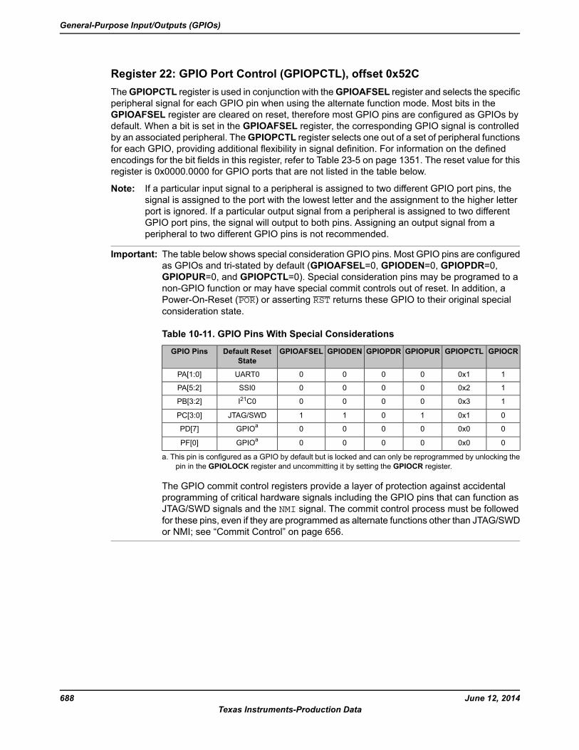
Register 22: GPIO Port Control (GPIOPCTL), offset 0x52C
TheGPIOPCTL register is used in conjunction with theGPIOAFSEL register and selects the specific
peripheral signal for each GPIO pin when using the alternate function mode. Most bits in the
GPIOAFSEL register are cleared on reset, therefore most GPIO pins are configured as GPIOs by
default. When a bit is set in the GPIOAFSEL register, the corresponding GPIO signal is controlled
by an associated peripheral. TheGPIOPCTL register selects one out of a set of peripheral functions
for each GPIO, providing additional flexibility in signal definition. For information on the defined
encodings for the bit fields in this register, refer to Table 23-5 on page 1351. The reset value for this
register is 0x0000.0000 for GPIO ports that are not listed in the table below.
Note: If a particular input signal to a peripheral is assigned to two different GPIO port pins, the
signal is assigned to the port with the lowest letter and the assignment to the higher letter
port is ignored. If a particular output signal from a peripheral is assigned to two different
GPIO port pins, the signal will output to both pins. Assigning an output signal from a
peripheral to two different GPIO pins is not recommended.
Important: The table below shows special consideration GPIO pins. Most GPIO pins are configured
as GPIOs and tri-stated by default (GPIOAFSEL=0, GPIODEN=0, GPIOPDR=0,
GPIOPUR=0, and GPIOPCTL=0). Special consideration pins may be programed to a
non-GPIO function or may have special commit controls out of reset. In addition, a
Power-On-Reset (POR) or asserting RST returns these GPIO to their original special
consideration state.
Table 10-11. GPIO Pins With Special Considerations
GPIOCRGPIOPCTLGPIOPURGPIOPDRGPIODENGPIOAFSELDefault Reset
State
GPIO Pins
10x10000UART0PA[1:0]
10x20000SSI0PA[5:2]
10x30000I21C0PB[3:2]
00x11011JTAG/SWDPC[3:0]
00x00000GPIOa
PD[7]
00x00000GPIOa
PF[0]
a. This pin is configured as a GPIO by default but is locked and can only be reprogrammed by unlocking the
pin in the GPIOLOCK register and uncommitting it by setting the GPIOCR register.
The GPIO commit control registers provide a layer of protection against accidental
programming of critical hardware signals including the GPIO pins that can function as
JTAG/SWD signals and the NMI signal. The commit control process must be followed
for these pins, even if they are programmed as alternate functions other than JTAG/SWD
or NMI; see “Commit Control” on page 656.
June 12, 2014688
Texas Instruments-Production Data
General-Purpose Input/Outputs (GPIOs)

GPIO Port Control (GPIOPCTL)
GPIO Port A (APB) base: 0x4000.4000GPIO Port A (AHB) base: 0x4005.8000GPIO Port B (APB) base: 0x4000.5000GPIO Port B (AHB) base: 0x4005.9000GPIO Port C (APB) base: 0x4000.6000GPIO Port C (AHB) base: 0x4005.A000GPIO Port D (APB) base: 0x4000.7000GPIO Port D (AHB) base: 0x4005.B000GPIO Port E (APB) base: 0x4002.4000GPIO Port E (AHB) base: 0x4005.C000GPIO Port F (APB) base: 0x4002.5000GPIO Port F (AHB) base: 0x4005.D000Offset 0x52CType RW, reset -
16171819202122232425262728293031
PMC4PMC5PMC6PMC7
RWRWRWRWRWRWRWRWRWRWRWRWRWRWRWRWType
----------------Reset
0123456789101112131415
PMC0PMC1PMC2PMC3
RWRWRWRWRWRWRWRWRWRWRWRWRWRWRWRWType
----------------Reset
DescriptionResetTypeNameBit/Field
Port Mux Control 7
This field controls the configuration for GPIO pin 7.
-RWPMC731:28
Port Mux Control 6
This field controls the configuration for GPIO pin 6.
-RWPMC627:24
Port Mux Control 5
This field controls the configuration for GPIO pin 5.
-RWPMC523:20
Port Mux Control 4
This field controls the configuration for GPIO pin 4.
-RWPMC419:16
Port Mux Control 3
This field controls the configuration for GPIO pin 3.
-RWPMC315:12
Port Mux Control 2
This field controls the configuration for GPIO pin 2.
-RWPMC211:8
Port Mux Control 1
This field controls the configuration for GPIO pin 1.
-RWPMC17:4
Port Mux Control 0
This field controls the configuration for GPIO pin 0.
-RWPMC03:0
689June 12, 2014
Texas Instruments-Production Data
Tiva™ TM4C123GH6PM Microcontroller

Register 23: GPIO ADC Control (GPIOADCCTL), offset 0x530
This register is used to configure a GPIO pin as a source for the ADC trigger.
Note that if the Port BGPIOADCCTL register is cleared, PB4 can still be used as an external trigger
for the ADC. This is a legacy mode which allows code written for previous devices to operate on
this microcontroller.
GPIO ADC Control (GPIOADCCTL)
GPIO Port A (APB) base: 0x4000.4000GPIO Port A (AHB) base: 0x4005.8000GPIO Port B (APB) base: 0x4000.5000GPIO Port B (AHB) base: 0x4005.9000GPIO Port C (APB) base: 0x4000.6000GPIO Port C (AHB) base: 0x4005.A000GPIO Port D (APB) base: 0x4000.7000GPIO Port D (AHB) base: 0x4005.B000GPIO Port E (APB) base: 0x4002.4000GPIO Port E (AHB) base: 0x4005.C000GPIO Port F (APB) base: 0x4002.5000GPIO Port F (AHB) base: 0x4005.D000Offset 0x530Type RW, reset 0x0000.0000
16171819202122232425262728293031
reserved
ROROROROROROROROROROROROROROROROType
0000000000000000Reset
0123456789101112131415
ADCENreserved
RWRWRWRWRWRWRWRWROROROROROROROROType
0000000000000000Reset
DescriptionResetTypeNameBit/Field
Software should not rely on the value of a reserved bit. To provide
compatibility with future products, the value of a reserved bit should be
preserved across a read-modify-write operation.
0x0000.00ROreserved31:8
ADC Trigger Enable
DescriptionValue
The corresponding pin is not used to trigger the ADC.0
The corresponding pin is used to trigger the ADC.1
0x00RWADCEN7:0
June 12, 2014690
Texas Instruments-Production Data
General-Purpose Input/Outputs (GPIOs)

Register 24: GPIO DMA Control (GPIODMACTL), offset 0x534
This register is used to configure a GPIO pin as a source for the μDMA trigger.
GPIO DMA Control (GPIODMACTL)
GPIO Port A (APB) base: 0x4000.4000GPIO Port A (AHB) base: 0x4005.8000GPIO Port B (APB) base: 0x4000.5000GPIO Port B (AHB) base: 0x4005.9000GPIO Port C (APB) base: 0x4000.6000GPIO Port C (AHB) base: 0x4005.A000GPIO Port D (APB) base: 0x4000.7000GPIO Port D (AHB) base: 0x4005.B000GPIO Port E (APB) base: 0x4002.4000GPIO Port E (AHB) base: 0x4005.C000GPIO Port F (APB) base: 0x4002.5000GPIO Port F (AHB) base: 0x4005.D000Offset 0x534Type RW, reset 0x0000.0000
16171819202122232425262728293031
reserved
ROROROROROROROROROROROROROROROROType
0000000000000000Reset
0123456789101112131415
DMAENreserved
RWRWRWRWRWRWRWRWROROROROROROROROType
0000000000000000Reset
DescriptionResetTypeNameBit/Field
Software should not rely on the value of a reserved bit. To provide
compatibility with future products, the value of a reserved bit should be
preserved across a read-modify-write operation.
0x0000.00ROreserved31:8
μDMA Trigger Enable
DescriptionValue
The corresponding pin is not used to trigger the μDMA.0
The corresponding pin is used to trigger the μDMA.1
0x00RWDMAEN7:0
691June 12, 2014
Texas Instruments-Production Data
Tiva™ TM4C123GH6PM Microcontroller

Register 25: GPIO Peripheral Identification 4 (GPIOPeriphID4), offset 0xFD0
The GPIOPeriphID4, GPIOPeriphID5, GPIOPeriphID6, and GPIOPeriphID7 registers can
conceptually be treated as one 32-bit register; each register contains eight bits of the 32-bit register,
used by software to identify the peripheral.
GPIO Peripheral Identification 4 (GPIOPeriphID4)
GPIO Port A (APB) base: 0x4000.4000GPIO Port A (AHB) base: 0x4005.8000GPIO Port B (APB) base: 0x4000.5000GPIO Port B (AHB) base: 0x4005.9000GPIO Port C (APB) base: 0x4000.6000GPIO Port C (AHB) base: 0x4005.A000GPIO Port D (APB) base: 0x4000.7000GPIO Port D (AHB) base: 0x4005.B000GPIO Port E (APB) base: 0x4002.4000GPIO Port E (AHB) base: 0x4005.C000GPIO Port F (APB) base: 0x4002.5000GPIO Port F (AHB) base: 0x4005.D000Offset 0xFD0Type RO, reset 0x0000.0000
16171819202122232425262728293031
reserved
ROROROROROROROROROROROROROROROROType
0000000000000000Reset
0123456789101112131415
PID4reserved
ROROROROROROROROROROROROROROROROType
0000000000000000Reset
DescriptionResetTypeNameBit/Field
Software should not rely on the value of a reserved bit. To provide
compatibility with future products, the value of a reserved bit should be
preserved across a read-modify-write operation.
0x0000.00ROreserved31:8
GPIO Peripheral ID Register [7:0]0x00ROPID47:0
June 12, 2014692
Texas Instruments-Production Data
General-Purpose Input/Outputs (GPIOs)

Register 26: GPIO Peripheral Identification 5 (GPIOPeriphID5), offset 0xFD4
The GPIOPeriphID4, GPIOPeriphID5, GPIOPeriphID6, and GPIOPeriphID7 registers can
conceptually be treated as one 32-bit register; each register contains eight bits of the 32-bit register,
used by software to identify the peripheral.
GPIO Peripheral Identification 5 (GPIOPeriphID5)
GPIO Port A (APB) base: 0x4000.4000GPIO Port A (AHB) base: 0x4005.8000GPIO Port B (APB) base: 0x4000.5000GPIO Port B (AHB) base: 0x4005.9000GPIO Port C (APB) base: 0x4000.6000GPIO Port C (AHB) base: 0x4005.A000GPIO Port D (APB) base: 0x4000.7000GPIO Port D (AHB) base: 0x4005.B000GPIO Port E (APB) base: 0x4002.4000GPIO Port E (AHB) base: 0x4005.C000GPIO Port F (APB) base: 0x4002.5000GPIO Port F (AHB) base: 0x4005.D000Offset 0xFD4Type RO, reset 0x0000.0000
16171819202122232425262728293031
reserved
ROROROROROROROROROROROROROROROROType
0000000000000000Reset
0123456789101112131415
PID5reserved
ROROROROROROROROROROROROROROROROType
0000000000000000Reset
DescriptionResetTypeNameBit/Field
Software should not rely on the value of a reserved bit. To provide
compatibility with future products, the value of a reserved bit should be
preserved across a read-modify-write operation.
0x0000.00ROreserved31:8
GPIO Peripheral ID Register [15:8]0x00ROPID57:0
693June 12, 2014
Texas Instruments-Production Data
Tiva™ TM4C123GH6PM Microcontroller

Register 27: GPIO Peripheral Identification 6 (GPIOPeriphID6), offset 0xFD8
The GPIOPeriphID4, GPIOPeriphID5, GPIOPeriphID6, and GPIOPeriphID7 registers can
conceptually be treated as one 32-bit register; each register contains eight bits of the 32-bit register,
used by software to identify the peripheral.
GPIO Peripheral Identification 6 (GPIOPeriphID6)
GPIO Port A (APB) base: 0x4000.4000GPIO Port A (AHB) base: 0x4005.8000GPIO Port B (APB) base: 0x4000.5000GPIO Port B (AHB) base: 0x4005.9000GPIO Port C (APB) base: 0x4000.6000GPIO Port C (AHB) base: 0x4005.A000GPIO Port D (APB) base: 0x4000.7000GPIO Port D (AHB) base: 0x4005.B000GPIO Port E (APB) base: 0x4002.4000GPIO Port E (AHB) base: 0x4005.C000GPIO Port F (APB) base: 0x4002.5000GPIO Port F (AHB) base: 0x4005.D000Offset 0xFD8Type RO, reset 0x0000.0000
16171819202122232425262728293031
reserved
ROROROROROROROROROROROROROROROROType
0000000000000000Reset
0123456789101112131415
PID6reserved
ROROROROROROROROROROROROROROROROType
0000000000000000Reset
DescriptionResetTypeNameBit/Field
Software should not rely on the value of a reserved bit. To provide
compatibility with future products, the value of a reserved bit should be
preserved across a read-modify-write operation.
0x0000.00ROreserved31:8
GPIO Peripheral ID Register [23:16]0x00ROPID67:0
June 12, 2014694
Texas Instruments-Production Data
General-Purpose Input/Outputs (GPIOs)
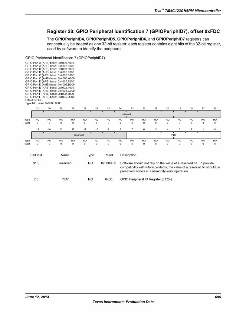
Register 28: GPIO Peripheral Identification 7 (GPIOPeriphID7), offset 0xFDC
The GPIOPeriphID4, GPIOPeriphID5, GPIOPeriphID6, and GPIOPeriphID7 registers can
conceptually be treated as one 32-bit register; each register contains eight bits of the 32-bit register,
used by software to identify the peripheral.
GPIO Peripheral Identification 7 (GPIOPeriphID7)
GPIO Port A (APB) base: 0x4000.4000GPIO Port A (AHB) base: 0x4005.8000GPIO Port B (APB) base: 0x4000.5000GPIO Port B (AHB) base: 0x4005.9000GPIO Port C (APB) base: 0x4000.6000GPIO Port C (AHB) base: 0x4005.A000GPIO Port D (APB) base: 0x4000.7000GPIO Port D (AHB) base: 0x4005.B000GPIO Port E (APB) base: 0x4002.4000GPIO Port E (AHB) base: 0x4005.C000GPIO Port F (APB) base: 0x4002.5000GPIO Port F (AHB) base: 0x4005.D000Offset 0xFDCType RO, reset 0x0000.0000
16171819202122232425262728293031
reserved
ROROROROROROROROROROROROROROROROType
0000000000000000Reset
0123456789101112131415
PID7reserved
ROROROROROROROROROROROROROROROROType
0000000000000000Reset
DescriptionResetTypeNameBit/Field
Software should not rely on the value of a reserved bit. To provide
compatibility with future products, the value of a reserved bit should be
preserved across a read-modify-write operation.
0x0000.00ROreserved31:8
GPIO Peripheral ID Register [31:24]0x00ROPID77:0
695June 12, 2014
Texas Instruments-Production Data
Tiva™ TM4C123GH6PM Microcontroller

Register 29: GPIO Peripheral Identification 0 (GPIOPeriphID0), offset 0xFE0
The GPIOPeriphID0, GPIOPeriphID1, GPIOPeriphID2, and GPIOPeriphID3 registers can
conceptually be treated as one 32-bit register; each register contains eight bits of the 32-bit register,
used by software to identify the peripheral.
GPIO Peripheral Identification 0 (GPIOPeriphID0)
GPIO Port A (APB) base: 0x4000.4000GPIO Port A (AHB) base: 0x4005.8000GPIO Port B (APB) base: 0x4000.5000GPIO Port B (AHB) base: 0x4005.9000GPIO Port C (APB) base: 0x4000.6000GPIO Port C (AHB) base: 0x4005.A000GPIO Port D (APB) base: 0x4000.7000GPIO Port D (AHB) base: 0x4005.B000GPIO Port E (APB) base: 0x4002.4000GPIO Port E (AHB) base: 0x4005.C000GPIO Port F (APB) base: 0x4002.5000GPIO Port F (AHB) base: 0x4005.D000Offset 0xFE0Type RO, reset 0x0000.0061
16171819202122232425262728293031
reserved
ROROROROROROROROROROROROROROROROType
0000000000000000Reset
0123456789101112131415
PID0reserved
ROROROROROROROROROROROROROROROROType
1000011000000000Reset
DescriptionResetTypeNameBit/Field
Software should not rely on the value of a reserved bit. To provide
compatibility with future products, the value of a reserved bit should be
preserved across a read-modify-write operation.
0x0000.00ROreserved31:8
GPIO Peripheral ID Register [7:0]
Can be used by software to identify the presence of this peripheral.
0x61ROPID07:0
June 12, 2014696
Texas Instruments-Production Data
General-Purpose Input/Outputs (GPIOs)

Register 30: GPIO Peripheral Identification 1 (GPIOPeriphID1), offset 0xFE4
The GPIOPeriphID0, GPIOPeriphID1, GPIOPeriphID2, and GPIOPeriphID3 registers can
conceptually be treated as one 32-bit register; each register contains eight bits of the 32-bit register,
used by software to identify the peripheral.
GPIO Peripheral Identification 1 (GPIOPeriphID1)
GPIO Port A (APB) base: 0x4000.4000GPIO Port A (AHB) base: 0x4005.8000GPIO Port B (APB) base: 0x4000.5000GPIO Port B (AHB) base: 0x4005.9000GPIO Port C (APB) base: 0x4000.6000GPIO Port C (AHB) base: 0x4005.A000GPIO Port D (APB) base: 0x4000.7000GPIO Port D (AHB) base: 0x4005.B000GPIO Port E (APB) base: 0x4002.4000GPIO Port E (AHB) base: 0x4005.C000GPIO Port F (APB) base: 0x4002.5000GPIO Port F (AHB) base: 0x4005.D000Offset 0xFE4Type RO, reset 0x0000.0000
16171819202122232425262728293031
reserved
ROROROROROROROROROROROROROROROROType
0000000000000000Reset
0123456789101112131415
PID1reserved
ROROROROROROROROROROROROROROROROType
0000000000000000Reset
DescriptionResetTypeNameBit/Field
Software should not rely on the value of a reserved bit. To provide
compatibility with future products, the value of a reserved bit should be
preserved across a read-modify-write operation.
0x0000.00ROreserved31:8
GPIO Peripheral ID Register [15:8]
Can be used by software to identify the presence of this peripheral.
0x00ROPID17:0
697June 12, 2014
Texas Instruments-Production Data
Tiva™ TM4C123GH6PM Microcontroller

Register 31: GPIO Peripheral Identification 2 (GPIOPeriphID2), offset 0xFE8
The GPIOPeriphID0, GPIOPeriphID1, GPIOPeriphID2, and GPIOPeriphID3 registers can
conceptually be treated as one 32-bit register; each register contains eight bits of the 32-bit register,
used by software to identify the peripheral.
GPIO Peripheral Identification 2 (GPIOPeriphID2)
GPIO Port A (APB) base: 0x4000.4000GPIO Port A (AHB) base: 0x4005.8000GPIO Port B (APB) base: 0x4000.5000GPIO Port B (AHB) base: 0x4005.9000GPIO Port C (APB) base: 0x4000.6000GPIO Port C (AHB) base: 0x4005.A000GPIO Port D (APB) base: 0x4000.7000GPIO Port D (AHB) base: 0x4005.B000GPIO Port E (APB) base: 0x4002.4000GPIO Port E (AHB) base: 0x4005.C000GPIO Port F (APB) base: 0x4002.5000GPIO Port F (AHB) base: 0x4005.D000Offset 0xFE8Type RO, reset 0x0000.0018
16171819202122232425262728293031
reserved
ROROROROROROROROROROROROROROROROType
0000000000000000Reset
0123456789101112131415
PID2reserved
ROROROROROROROROROROROROROROROROType
0001100000000000Reset
DescriptionResetTypeNameBit/Field
Software should not rely on the value of a reserved bit. To provide
compatibility with future products, the value of a reserved bit should be
preserved across a read-modify-write operation.
0x0000.00ROreserved31:8
GPIO Peripheral ID Register [23:16]
Can be used by software to identify the presence of this peripheral.
0x18ROPID27:0
June 12, 2014698
Texas Instruments-Production Data
General-Purpose Input/Outputs (GPIOs)

Register 32: GPIO Peripheral Identification 3 (GPIOPeriphID3), offset 0xFEC
The GPIOPeriphID0, GPIOPeriphID1, GPIOPeriphID2, and GPIOPeriphID3 registers can
conceptually be treated as one 32-bit register; each register contains eight bits of the 32-bit register,
used by software to identify the peripheral.
GPIO Peripheral Identification 3 (GPIOPeriphID3)
GPIO Port A (APB) base: 0x4000.4000GPIO Port A (AHB) base: 0x4005.8000GPIO Port B (APB) base: 0x4000.5000GPIO Port B (AHB) base: 0x4005.9000GPIO Port C (APB) base: 0x4000.6000GPIO Port C (AHB) base: 0x4005.A000GPIO Port D (APB) base: 0x4000.7000GPIO Port D (AHB) base: 0x4005.B000GPIO Port E (APB) base: 0x4002.4000GPIO Port E (AHB) base: 0x4005.C000GPIO Port F (APB) base: 0x4002.5000GPIO Port F (AHB) base: 0x4005.D000Offset 0xFECType RO, reset 0x0000.0001
16171819202122232425262728293031
reserved
ROROROROROROROROROROROROROROROROType
0000000000000000Reset
0123456789101112131415
PID3reserved
ROROROROROROROROROROROROROROROROType
1000000000000000Reset
DescriptionResetTypeNameBit/Field
Software should not rely on the value of a reserved bit. To provide
compatibility with future products, the value of a reserved bit should be
preserved across a read-modify-write operation.
0x0000.00ROreserved31:8
GPIO Peripheral ID Register [31:24]
Can be used by software to identify the presence of this peripheral.
0x01ROPID37:0
699June 12, 2014
Texas Instruments-Production Data
Tiva™ TM4C123GH6PM Microcontroller

Register 33: GPIO PrimeCell Identification 0 (GPIOPCellID0), offset 0xFF0
TheGPIOPCellID0,GPIOPCellID1,GPIOPCellID2, andGPIOPCellID3 registers are four 8-bit wide
registers, that can conceptually be treated as one 32-bit register. The register is used as a standard
cross-peripheral identification system.
GPIO PrimeCell Identification 0 (GPIOPCellID0)
GPIO Port A (APB) base: 0x4000.4000GPIO Port A (AHB) base: 0x4005.8000GPIO Port B (APB) base: 0x4000.5000GPIO Port B (AHB) base: 0x4005.9000GPIO Port C (APB) base: 0x4000.6000GPIO Port C (AHB) base: 0x4005.A000GPIO Port D (APB) base: 0x4000.7000GPIO Port D (AHB) base: 0x4005.B000GPIO Port E (APB) base: 0x4002.4000GPIO Port E (AHB) base: 0x4005.C000GPIO Port F (APB) base: 0x4002.5000GPIO Port F (AHB) base: 0x4005.D000Offset 0xFF0Type RO, reset 0x0000.000D
16171819202122232425262728293031
reserved
ROROROROROROROROROROROROROROROROType
0000000000000000Reset
0123456789101112131415
CID0reserved
ROROROROROROROROROROROROROROROROType
1011000000000000Reset
DescriptionResetTypeNameBit/Field
Software should not rely on the value of a reserved bit. To provide
compatibility with future products, the value of a reserved bit should be
preserved across a read-modify-write operation.
0x0000.00ROreserved31:8
GPIO PrimeCell ID Register [7:0]
Provides software a standard cross-peripheral identification system.
0x0DROCID07:0
June 12, 2014700
Texas Instruments-Production Data
General-Purpose Input/Outputs (GPIOs)
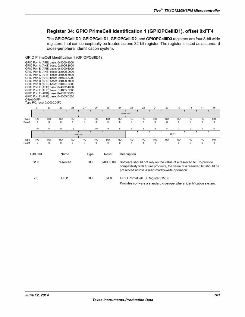
Register 34: GPIO PrimeCell Identification 1 (GPIOPCellID1), offset 0xFF4
TheGPIOPCellID0,GPIOPCellID1,GPIOPCellID2, andGPIOPCellID3 registers are four 8-bit wide
registers, that can conceptually be treated as one 32-bit register. The register is used as a standard
cross-peripheral identification system.
GPIO PrimeCell Identification 1 (GPIOPCellID1)
GPIO Port A (APB) base: 0x4000.4000GPIO Port A (AHB) base: 0x4005.8000GPIO Port B (APB) base: 0x4000.5000GPIO Port B (AHB) base: 0x4005.9000GPIO Port C (APB) base: 0x4000.6000GPIO Port C (AHB) base: 0x4005.A000GPIO Port D (APB) base: 0x4000.7000GPIO Port D (AHB) base: 0x4005.B000GPIO Port E (APB) base: 0x4002.4000GPIO Port E (AHB) base: 0x4005.C000GPIO Port F (APB) base: 0x4002.5000GPIO Port F (AHB) base: 0x4005.D000Offset 0xFF4Type RO, reset 0x0000.00F0
16171819202122232425262728293031
reserved
ROROROROROROROROROROROROROROROROType
0000000000000000Reset
0123456789101112131415
CID1reserved
ROROROROROROROROROROROROROROROROType
0000111100000000Reset
DescriptionResetTypeNameBit/Field
Software should not rely on the value of a reserved bit. To provide
compatibility with future products, the value of a reserved bit should be
preserved across a read-modify-write operation.
0x0000.00ROreserved31:8
GPIO PrimeCell ID Register [15:8]
Provides software a standard cross-peripheral identification system.
0xF0ROCID17:0
701June 12, 2014
Texas Instruments-Production Data
Tiva™ TM4C123GH6PM Microcontroller

Register 35: GPIO PrimeCell Identification 2 (GPIOPCellID2), offset 0xFF8
TheGPIOPCellID0,GPIOPCellID1,GPIOPCellID2, andGPIOPCellID3 registers are four 8-bit wide
registers, that can conceptually be treated as one 32-bit register. The register is used as a standard
cross-peripheral identification system.
GPIO PrimeCell Identification 2 (GPIOPCellID2)
GPIO Port A (APB) base: 0x4000.4000GPIO Port A (AHB) base: 0x4005.8000GPIO Port B (APB) base: 0x4000.5000GPIO Port B (AHB) base: 0x4005.9000GPIO Port C (APB) base: 0x4000.6000GPIO Port C (AHB) base: 0x4005.A000GPIO Port D (APB) base: 0x4000.7000GPIO Port D (AHB) base: 0x4005.B000GPIO Port E (APB) base: 0x4002.4000GPIO Port E (AHB) base: 0x4005.C000GPIO Port F (APB) base: 0x4002.5000GPIO Port F (AHB) base: 0x4005.D000Offset 0xFF8Type RO, reset 0x0000.0005
16171819202122232425262728293031
reserved
ROROROROROROROROROROROROROROROROType
0000000000000000Reset
0123456789101112131415
CID2reserved
ROROROROROROROROROROROROROROROROType
1010000000000000Reset
DescriptionResetTypeNameBit/Field
Software should not rely on the value of a reserved bit. To provide
compatibility with future products, the value of a reserved bit should be
preserved across a read-modify-write operation.
0x0000.00ROreserved31:8
GPIO PrimeCell ID Register [23:16]
Provides software a standard cross-peripheral identification system.
0x05ROCID27:0
June 12, 2014702
Texas Instruments-Production Data
General-Purpose Input/Outputs (GPIOs)

Register 36: GPIO PrimeCell Identification 3 (GPIOPCellID3), offset 0xFFC
TheGPIOPCellID0,GPIOPCellID1,GPIOPCellID2, andGPIOPCellID3 registers are four 8-bit wide
registers, that can conceptually be treated as one 32-bit register. The register is used as a standard
cross-peripheral identification system.
GPIO PrimeCell Identification 3 (GPIOPCellID3)
GPIO Port A (APB) base: 0x4000.4000GPIO Port A (AHB) base: 0x4005.8000GPIO Port B (APB) base: 0x4000.5000GPIO Port B (AHB) base: 0x4005.9000GPIO Port C (APB) base: 0x4000.6000GPIO Port C (AHB) base: 0x4005.A000GPIO Port D (APB) base: 0x4000.7000GPIO Port D (AHB) base: 0x4005.B000GPIO Port E (APB) base: 0x4002.4000GPIO Port E (AHB) base: 0x4005.C000GPIO Port F (APB) base: 0x4002.5000GPIO Port F (AHB) base: 0x4005.D000Offset 0xFFCType RO, reset 0x0000.00B1
16171819202122232425262728293031
reserved
ROROROROROROROROROROROROROROROROType
0000000000000000Reset
0123456789101112131415
CID3reserved
ROROROROROROROROROROROROROROROROType
1000110100000000Reset
DescriptionResetTypeNameBit/Field
Software should not rely on the value of a reserved bit. To provide
compatibility with future products, the value of a reserved bit should be
preserved across a read-modify-write operation.
0x0000.00ROreserved31:8
GPIO PrimeCell ID Register [31:24]
Provides software a standard cross-peripheral identification system.
0xB1ROCID37:0
703June 12, 2014
Texas Instruments-Production Data
Tiva™ TM4C123GH6PM Microcontroller