Embed Size (px)
Citation preview

TMP814
Vm
Speed Setting
Vover
Lock Detection
Speed Output
Frequency Set
Current Limit
H+
H-
RF
Limit Vcc(Optional)
Product
Folder
Sample &Buy
Technical
Documents
Tools &
Software
Support &Community
TMP814SLDS151A –MAY 2009–REVISED JUNE 2015
TMP814 Variable Speed Single-phase Full-wave Fan Motor Predriver1
1 Features• Predriver for Single-Phase Full-Wave Drive • Lock Protection and Automatic Reset Functions
Incorporated– PNP-NMOS is Used as an External Power TR,• FG (Rotation Speed Detection) and RD (LockEnabling High-Efficiency Low-Consumption
Detection) OutputDrive by Means of the Low-Saturation Outputand Single-Phase Full-Wave Drive (PMOS-
2 ApplicationsNMOS Also Applicable)• External PWM Input Enabling Variable Speed • Server Fans (Up to 48 V)
Control • Appliance Fans (Up to 48 V)– Separately-Excited Upper Direct PWM (f = 25
kHz) Control Method, Enabling Highly Silent 3 DescriptionSpeed Control The TMP814 is a single-phase bipolar variable speed
fan motor predriver that works with an external PWM• Compatible with 12-V, 24-V, and 48-V Powersignal. A highly efficient, quiet and low-powerSuppliesconsumption motor driver circuit, with a large variable• Current Limiter Circuit Incorporated speed, can be implemented by adding a small
– Chopper Type Current Limit at Start number of external components.• Reactive Current Cut Circuit Incorporated This device is optimal for driving large scale fan
– Reactive Current Before Phase Change is Cut motors (with large air volume and large current) suchto Enable Silent and Low-Consumption Drive as those used in servers and consumer products.
• Minimum Speed Setting PinDevice Information(1)
– Minimum Speed Can Be Set With ExternalPART NUMBER PACKAGE BODY SIZE (NOM)Resistor. Start Assistance Circuit Enables Start
TMP814 TSSOP (PW) 4.40 mm x 6.50 mmat Extremely Low Speed.(1) For all available packages, see the orderable addendum at• Constant-Voltage Output Pin for Hall Bias
the end of the data sheet.
Simplified Schematic
1
An IMPORTANT NOTICE at the end of this data sheet addresses availability, warranty, changes, use in safety-critical applications,intellectual property matters and other important disclaimers. PRODUCTION DATA.

TMP814SLDS151A –MAY 2009–REVISED JUNE 2015 www.ti.com
Table of Contents7.3 Feature Description................................................... 81 Features .................................................................. 17.4 Device Functional Modes........................................ 102 Applications ........................................................... 1
8 Application and Implementation ........................ 113 Description ............................................................. 18.1 Application Information............................................ 114 Revision History..................................................... 28.2 Typical Applications ............................................... 125 Pin Configuration and Functions ......................... 3
9 Power Supply Recommendations ...................... 156 Specifications......................................................... 410 Layout................................................................... 156.1 Absolute Maximum Ratings ..................................... 4
10.1 Layout Guidelines ................................................. 156.2 ESD Ratings ............................................................ 410.2 Layout Example .................................................... 156.3 Recommended Operating Conditions....................... 4
11 Device and Documentation Support ................. 166.4 Thermal Information .................................................. 411.1 Community Resources.......................................... 166.5 Electrical Characteristics........................................... 511.2 Trademarks ........................................................... 166.6 Typical Characteristics .............................................. 711.3 Electrostatic Discharge Caution............................ 167 Detailed Description .............................................. 811.4 Glossary ................................................................ 167.1 Overview ................................................................... 8
12 Mechanical, Packaging, and Orderable7.2 Functional Block Diagram ......................................... 8Information ........................................................... 16
4 Revision History
Changes from Original (May 2009) to Revision A Page
• Added ESD Ratings table, Feature Description section, Device Functional Modes, Application and Implementationsection, Power Supply Recommendations section, Layout section, Device and Documentation Support section, andMechanical, Packaging, and Orderable Information section. ................................................................................................. 1
2 Submit Documentation Feedback Copyright © 2009–2015, Texas Instruments Incorporated
Product Folder Links: TMP814

1
2
3
4
5
6
7
8
9
10 11
12
13
14
15
16
17
18
19
20OUT2P
OUT2N
VCC
VLIM
SENSE
RMI
VTH
CPWM
FG
RD
OUT1P
OUT1N
VOVER
SGND
6VREG
ROFF
CT
IN+
HB
IN–
TMP814www.ti.com SLDS151A –MAY 2009–REVISED JUNE 2015
5 Pin Configuration and Functions
PW Package20-Pin TSSOP
Top View
Pin FunctionsPIN
I/O DESCRIPTIONNO. NAME1 OUT2P O Upper-side driver output2 OUT2N O Lower-side driver output
Power supply. For the CM capacitor that is a power stabilization capacitor for PWM drive and forabsorption of kickback, the capacitance of 0.1 μF to 1 μF is used. In this device, the lower TR
3 VCC performs current regeneration by switching the upper TR. Connect CM between VCC and GND,with the thick pattern and along the shortest route. Use a zener diode if kickback causesexcessive increase of the supply voltage, because such increase may damage the device.Activates the current limiter when SENSE voltage is greater than VLIM voltage. Connect to4 VLIM I 6VREG when not used.
5 SENSE I Sense input. Connect to GND when not used.Minimum speed setting. Connect to 6VREG when not used. If device power can be removed
6 RMI I before power is removed from RMI, insert a current limiting resistor to prevent inflow of largecurrent.
7 VTH I VTH : Connect to GND if not used (Full Speed).Connect to capacitor CP to set the PWM oscillation frequency. With CP = 100 pF, oscillation8 CPWM O occurs at 25 kHz and provides the basic frequency of PWM.Open collector output, which can detect the rotation speed using the FG output according to the9 FG O phase shift. Leave open when not used.
10 RD O Open collector output. Outputs low during rotation and high at stop. Leave open when not used.11 IN– I Hall input12 HB O This is a Hall element bias, that is, the 1.5-V constant-voltage output.
Hall input. Make connecting traces as short as possible to prevent carrying of noise. To futherlimit noise, insert a capacitor between IN+ and IN–. The Hall input circuit is a comparator having13 IN+ I a hysteresis of 20 mV. The application should ensure that the Hall input level more than threetimes (60 mVp-p) this hysteresis.
14 CT O Lock detection time setting. Capacitor CT is connected.Sets the soft switching time to cut the reactive current before phase change. Connect to 6VREG15 ROFF I when not used.
16 6VREG O 6-V regulator output17 SGND Connected to the control circuit power supply system.
Constant-voltage bias and should be used for application of 24 V and 48 V (see Figure 7). A18 VOVER O current limiting resistor should be used. Leave open when not used.19 OUT1N O Lower-side driver output20 OUT1P O Upper-side driver output
Copyright © 2009–2015, Texas Instruments Incorporated Submit Documentation Feedback 3
Product Folder Links: TMP814

TMP814SLDS151A –MAY 2009–REVISED JUNE 2015 www.ti.com
6 Specifications
6.1 Absolute Maximum Ratingsover operating free-air temperature range (unless otherwise noted) (1)
MIN MAX UNITVCC Supply voltage 18 VVOUT Output voltage OUT1P, OUT1N, OUT2P, OUT2N 18 VIOUT Continuous output current OUT1P, OUT1N, OUT2P, OUT2N 50 mAIHB Continuous output current HB 10 mAVTH Input voltage VTH 8 VVRD Output voltage RD, FG 18 VVFG
IRD Continuous output current RD, FG 10 mAIFG
Tstg Storage temperature –65 150 °C
(1) Stresses beyond those listed under "absolute maximum ratings" may cause permanent damage to the device. These are stress ratingsonly, and functional operation of the device at these or any other conditions beyond those indicated under "recommended operatingconditions" is not implied. Exposure to absolute-maximum-rated conditions for extended periods may affect device reliability.
6.2 ESD RatingsVALUE UNIT
Human body model (HBM), per ANSI/ESDA/JEDEC JS-001, all pins (1) ±2500V(ESD) Electrostatic discharge VCharged device model (CDM), per JEDEC specification JESD22-C101, all ±1000pins (2)
(1) JEDEC document JEP155 states that 500-V HBM allows safe manufacturing with a standard ESD control process.(2) JEDEC document JEP157 states that 250-V CDM allows safe manufacturing with a standard ESD control process.
6.3 Recommended Operating ConditionsTA = 25°C
MIN MAX UNITVCC Supply voltage 6 16 VVTH VTH input voltage Full-speed mode 0 7 VVICM Hall input common phase input voltage 0.2 3 VTA Operating free-air temperature –30 95 °C
6.4 Thermal InformationTMP814
THERMAL METRIC (1) PW (TSSOP) UNIT20 PINS
RθJA Junction-to-ambient thermal resistance 83 °C/WRθJC(top) Junction-to-case (top) thermal resistance 90.6 °C/WRθJB Junction-to-board thermal resistance 42.1 °C/WψJT Junction-to-top characterization parameter 24.3 °C/WψJB Junction-to-board characterization parameter 0.9 °C/WRθJC(bot) Junction-to-case (bottom) thermal resistance 41.5 °C/W
(1) For more information about traditional and new thermal metrics, see the Semiconductor and IC Package Thermal Metrics applicationreport, SPRA953.
4 Submit Documentation Feedback Copyright © 2009–2015, Texas Instruments Incorporated
Product Folder Links: TMP814
TMP814www.ti.com SLDS151A –MAY 2009–REVISED JUNE 2015
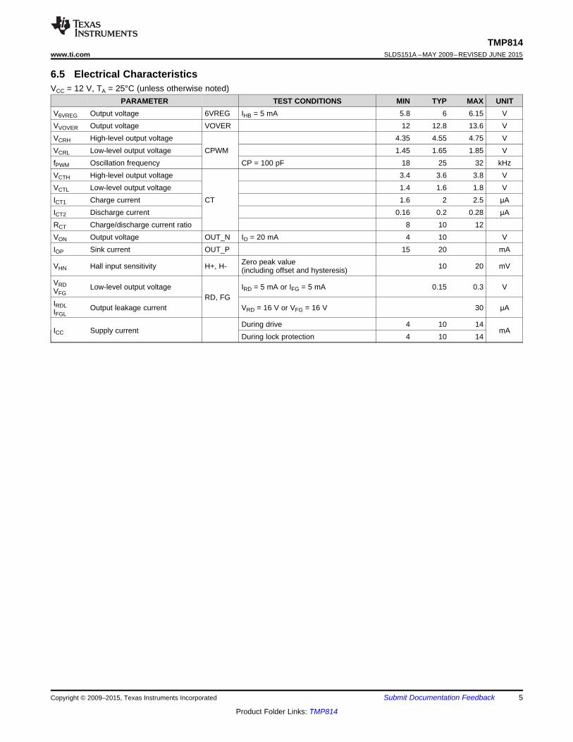
6.5 Electrical CharacteristicsVCC = 12 V, TA = 25°C (unless otherwise noted)
PARAMETER TEST CONDITIONS MIN TYP MAX UNITV6VREG Output voltage 6VREG IHB = 5 mA 5.8 6 6.15 VVVOVER Output voltage VOVER 12 12.8 13.6 VVCRH High-level output voltage 4.35 4.55 4.75 VVCRL Low-level output voltage CPWM 1.45 1.65 1.85 VfPWM Oscillation frequency CP = 100 pF 18 25 32 kHzVCTH High-level output voltage 3.4 3.6 3.8 VVCTL Low-level output voltage 1.4 1.6 1.8 VICT1 Charge current CT 1.6 2 2.5 μAICT2 Discharge current 0.16 0.2 0.28 μARCT Charge/discharge current ratio 8 10 12VON Output voltage OUT_N IO = 20 mA 4 10 VIOP Sink current OUT_P 15 20 mA
Zero peak valueVHN Hall input sensitivity H+, H- 10 20 mV(including offset and hysteresis)VRD Low-level output voltage IRD = 5 mA or IFG = 5 mA 0.15 0.3 VVFG RD, FGIRDL Output leakage current VRD = 16 V or VFG = 16 V 30 μAIFGL
During drive 4 10 14ICC Supply current mA
During lock protection 4 10 14
Copyright © 2009–2015, Texas Instruments Incorporated Submit Documentation Feedback 5
Product Folder Links: TMP814

0 V
CPWM
VCC
FG
0 V
VTH voltage
RMI voltage
4.55 V
1.65 V
PWM-IN disconnected
ON duty small
f = 25 kHz (CP = 100 pF) ON duty large
PWM controlvariable speed
Full speed
12 V
Rotation set tominimum speed
(stop mode)
Low speed High speed
TMP814SLDS151A –MAY 2009–REVISED JUNE 2015 www.ti.com
A. Minimum speed setting (stop) modePWM-IN input is filtered to generate the VTH voltage. At low speed, the fan rotates with the minimum speed set withRMI during low speed. If the minimum speed is not set (RMI = 6VREG), the fan stops.
B. Low ↔ high speed modePWM control is made through comparison of oscillation and VTH voltages with CPWM changing between 1.6 V ↔ 4.6V.Upper and lower TRs are turned ON when the VTH voltage is greater. The upper output TR is turned OFF when theVTH voltage is lower, and the coil current is regenerated in the lower TR. Therefore, as the VTH voltage lowers, theoutput ON duty increases, increasing the coil current and raising the motor speed. The rotation speed is fed back bythe FG output.
C. Full speed modeThe full-speed mode becomes effective with the VTH voltage of 1.65 V or less. (VTH must be equal to GND when thespeed control is not used.)
D. PWM-IN input disconnection modeWhen the PWM-IN input pin is disconnected, VTH becomes 1.65 V or less and the output enables full drive at 100%.The fan runs at full speed (see Figure 3).
Figure 1. Control Timing
6 Submit Documentation Feedback Copyright © 2009–2015, Texas Instruments Incorporated
Product Folder Links: TMP814

Output Current (mA)
6VR
EG
OU
T (
V)
0 5 10 15 20 25 304
4.5
5
5.5
6
6.5
D001
6VREG Output-9V6VREG Output-12V6VREG Output-15V
TMP814www.ti.com SLDS151A –MAY 2009–REVISED JUNE 2015
6.6 Typical Characteristics
Figure 2. 6VREGOUT Load Regulation
Copyright © 2009–2015, Texas Instruments Incorporated Submit Documentation Feedback 7
Product Folder Links: TMP814

0.47 µFto 1 µF
VCC
6VREG
ROFF
HB
IN+
IN–
RMI CPWM VLIM SENSE SGND
OUT2P
OUT2N
OUT1P
OUT1N
RD
FG
Discharge Circuit
DischargePulse
6VREG
Hall Bias
HysteresisAmplifier
Thermal Shutdown Oscillator
Controller
CT
Hall
VTH
TMP814SLDS151A –MAY 2009–REVISED JUNE 2015 www.ti.com
7 Detailed Description
7.1 OverviewThe TMP814 device is a single phase bipolar predriver which uses the hall sensor & speed control inputs fordriving the single phase motor connected through H Bridge. The predriver outputs are designed for driving topside P-type devices and bottom side N-channel FETs in the bridge. Multiple protections like overcurrent, soft-start, speed control, lock detect, speed feedback and minimum speed are incorporated in the device. The circuitcan be used for driving the 24-V or 48-V system using a VOVER pin, which protects the VCC to be less than thelimit of 18 V.
7.2 Functional Block Diagram
7.3 Feature Description
7.3.1 Speed ControlThe speed control functionality is obtained by VTH pin of the device. For pulsed inputs user can supply a 20 kHz-100 kHz frequency input (20 kHz to 50 kHz recommended on the pin with a current limiting resistor in between. Ifnot used, this pin needs to be connected to ground for full speed.
8 Submit Documentation Feedback Copyright © 2009–2015, Texas Instruments Incorporated
Product Folder Links: TMP814

TMP814www.ti.com SLDS151A –MAY 2009–REVISED JUNE 2015
Feature Description (continued)7.3.2 Constant Voltage BiasConstant Voltage Bias is provided through VOVER Pin. This must be used for applications of 24 V and 48 V.See Figure 3. This drive limits the VCC under permissible values even when Vm > 18 V. Leave this pin openwhen not in use.
7.3.3 Soft-StartSoft-Start Time can be using the ROFF pin. Connect 6 to 6VREG is not used.
7.3.4 Lock DetectionWhen the rotor is locked by external means or load conditions, The lock detection feature helps to protect thecircuit by not allowing the current to rise beyond control. A hiccup mechanism is also provided. The lockdetection is enabled by a connection to the lock detection capacitor. When the pin voltage rises to 1.2 V, theconstant current charge and discharge circuits cause the drive to and enables it back when voltage reaches 0. Iflock detection feature is not desired in the application, then this pin must be connected to ground.
7.3.5 Current LimitCurrent limit resistor is connected in a return path of H Bridge connection. This input is connected to the SENSEpin where the Current is limited when the voltage across this resistor crosses the voltage at VLIM Pin. If notused, this pin needs to be connected to ground.
7.3.6 Minimum Speed SettingMinimum speed setting feature is used with the RMI pin in the device. Connect to 6VREG with a pullup resistor ifnot used.
7.3.7 Speed OutputThe speed of the motor while running can be observed at the FG pin which is an open collector output andneeds to be pulled high for using it.
7.3.8 Drive Frequency SelectionThe P channel switches in the device are switched with higher frequency whose duty cycle is decided by thespeed control input. The frequency of the operation can be decided by the capacitor connected at the CPWMpin. As this is used also for the current limiting canceling signal, be sure to connect the capacitor even whenspeed control is not used.
Copyright © 2009–2015, Texas Instruments Incorporated Submit Documentation Feedback 9
Product Folder Links: TMP814

TMP814SLDS151A –MAY 2009–REVISED JUNE 2015 www.ti.com
7.4 Device Functional Modes
Table 1. Truth Table (1)
IN– IN+ CT OUT1P OUT1N OUT2P OUT2N FG RD MODEH L L L – – H L L OUT1 → 2 driveL H – H L – OFF OUT2 → 1 driveH L H OFF – – H L OFF Lock protectionL H – H OFF – OFF
(1) During full-speed rotation
VTH CPWM IN– IN+ OUT1P OUT1N OUT2P OUT2N MODEH L L – – H OUT1 → 2 Drive
L HL H – H L – OUT2 → 1 DriveH L OFF – – H During rotation,H L regeneration in lower TRL H – H OFF –
10 Submit Documentation Feedback Copyright © 2009–2015, Texas Instruments Incorporated
Product Folder Links: TMP814
TMP814www.ti.com SLDS151A –MAY 2009–REVISED JUNE 2015
8 Application and Implementation
NOTEInformation in the following applications sections is not part of the TI componentspecification, and TI does not warrant its accuracy or completeness. TI’s customers areresponsible for determining suitability of components for their purposes. Customers shouldvalidate and test their design implementation to confirm system functionality.
8.1 Application InformationThe TMP814 device requires few external components for the features described in Feature Description. Thedevice needs a 1-uF or more capacitor connected at VCC. The device generates 6-V regulated output which canbe used for pullups in the circuit as well as the Hall sensor.
Copyright © 2009–2015, Texas Instruments Incorporated Submit Documentation Feedback 11
Product Folder Links: TMP814

SOP8901
RF
CB = ~ 0.022 µF
RB = 10 k
ROUT = 100
W
W
VCC
VOVER
HB
IN–
IN+
RMI
VTH
CPWM
CT
SGND
OUT2N
OUT2P
OUT1N
OUT1P
ROFF
6VREG
VLIM
SENSE
FG
RD
R , R = 10 k to 100FG RD W W
CT = 0.47 µF
CP = 100 pF
25 kHz
R = 0 to 5 kW
H
6VREG
PWM-IN
TMP814SLDS151A –MAY 2009–REVISED JUNE 2015 www.ti.com
8.2 Typical Applications
8.2.1 12-V Sample Application Circuit
Figure 3. 12-V Sample Application Circuit
8.2.1.1 Design RequirementsInput Voltage: 6 to 16 V
VCC capacitor: 1 uF or more
H Bridge top side: P-channel FETs
H Bridge bottom side: N-channel FETs
8.2.1.2 Detailed Design ProcedurePins:• CPWM Capacitor: 100 pF for 25 kHz switching or appropriate.
12 Submit Documentation Feedback Copyright © 2009–2015, Texas Instruments Incorporated
Product Folder Links: TMP814

TMP814www.ti.com SLDS151A –MAY 2009–REVISED JUNE 2015
Typical Applications (continued)• VTH Pin connected to Ground for Full speed or supplied with pulsed input.• RMI Pin Pulled high to 6VREG output or external connection if required.• ROFF pulled to 6VREG.• 6VREG connected to Hall Sensor. Hall sensor differential inputs connected to IN+ and IN-.• SENSE pin or GND.• CT connected to Lock Detection capacitor (0.47uF or calculated values)or to GND.• Drive outputs connected to the Gates of the H bridge switches.• Pullup on FG.• VLIM and VOVER kept open.
Power Supply:• Make sure the power supply has set with sufficient current limit at the decided at the motor voltage.
Build the circuit with previously recommended connections at the pins.
Test the motor circuit with hardware connected to it.
8.2.1.3 Application Curves
Figure 4. Start-up at 12 V Figure 5. Motor Outputs and Phase Current at 100% DutyCycle
Figure 6. Lock Detection Waveform
Copyright © 2009–2015, Texas Instruments Incorporated Submit Documentation Feedback 13
Product Folder Links: TMP814
RF
VCC
VOVER
HB
IN–
IN+
RMI
VTH
CPWM
CT
SGND
OUT2N
OUT2P
OUT1N
OUT1P
ROFF
6VREG
VLIM
SENSE
FG
RD
CT = 0.47 µF
CP = 100 pF
H
6VREG
PWM-IN
TMP814SLDS151A –MAY 2009–REVISED JUNE 2015 www.ti.com
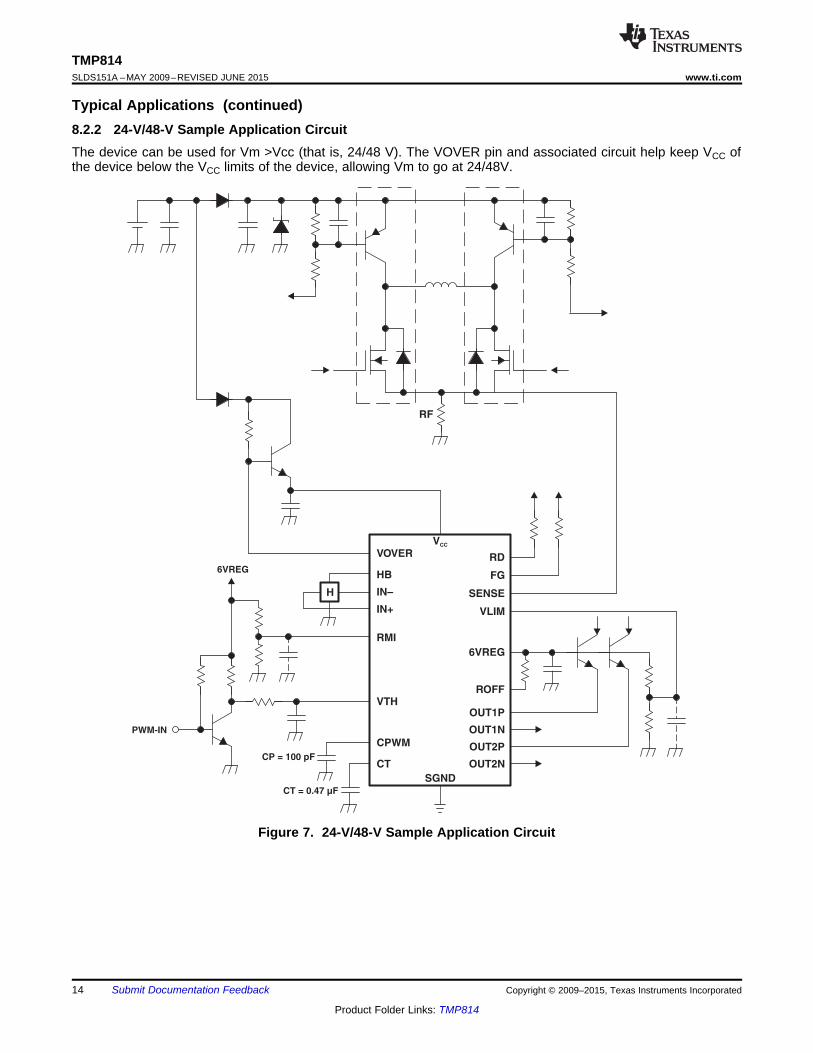
Typical Applications (continued)8.2.2 24-V/48-V Sample Application CircuitThe device can be used for Vm >Vcc (that is, 24/48 V). The VOVER pin and associated circuit help keep VCC ofthe device below the VCC limits of the device, allowing Vm to go at 24/48V.
Figure 7. 24-V/48-V Sample Application Circuit
14 Submit Documentation Feedback Copyright © 2009–2015, Texas Instruments Incorporated
Product Folder Links: TMP814

6VREG
OUT2P
OUT2N
VCC
VLIM
SENSE
OUT1P
OUT1N
VOVER
SGND
6VREG
TMP814
GND
RMI
VTH
CPWM
ROFF
CT
IN+
>1uF
FG HB
IN±
TMP814www.ti.com SLDS151A –MAY 2009–REVISED JUNE 2015
9 Power Supply RecommendationsFor testing purposes, a current limited source can be connected with voltage from 6 V to 16 V on printed-circuit-board. Use a 1-µF capacitor (minimum) to take care of load transient requirements.
10 Layout
10.1 Layout GuidelinesConnect a minimum of 1-µF or greater capacitor close to the power supply pins. Connect other capacitors andresistors according to the calculations (for example, the pullup resistors should be connected at various pins, thec capacitors should be connected at lock detect, and so forth.)
10.2 Layout Example
Figure 8. Recommended Layout
Copyright © 2009–2015, Texas Instruments Incorporated Submit Documentation Feedback 15
Product Folder Links: TMP814

TMP814SLDS151A –MAY 2009–REVISED JUNE 2015 www.ti.com
11 Device and Documentation Support
11.1 Community ResourcesThe following links connect to TI community resources. Linked contents are provided "AS IS" by the respectivecontributors. They do not constitute TI specifications and do not necessarily reflect TI's views; see TI's Terms ofUse.
TI E2E™ Online Community TI's Engineer-to-Engineer (E2E) Community. Created to foster collaborationamong engineers. At e2e.ti.com, you can ask questions, share knowledge, explore ideas and helpsolve problems with fellow engineers.
Design Support TI's Design Support Quickly find helpful E2E forums along with design support tools andcontact information for technical support.
11.2 TrademarksE2E is a trademark of Texas Instruments.All other trademarks are the property of their respective owners.
11.3 Electrostatic Discharge CautionThese devices have limited built-in ESD protection. The leads should be shorted together or the device placed in conductive foamduring storage or handling to prevent electrostatic damage to the MOS gates.
11.4 GlossarySLYZ022 — TI Glossary.
This glossary lists and explains terms, acronyms, and definitions.
12 Mechanical, Packaging, and Orderable InformationThe following pages include mechanical, packaging, and orderable information. This information is the mostcurrent data available for the designated devices. This data is subject to change without notice and revision ofthis document. For browser-based versions of this data sheet, refer to the left-hand navigation.
16 Submit Documentation Feedback Copyright © 2009–2015, Texas Instruments Incorporated
Product Folder Links: TMP814

TAPE AND REEL INFORMATION
*All dimensions are nominal
Device PackageType
PackageDrawing
Pins SPQ ReelDiameter
(mm)
ReelWidth
W1 (mm)
A0(mm)
B0(mm)
K0(mm)
P1(mm)
W(mm)
Pin1Quadrant
TMP814PWR TSSOP PW 20 2000 330.0 16.4 6.95 7.1 1.6 8.0 16.0 Q1
PACKAGE MATERIALS INFORMATION
www.ti.com 29-May-2015
Pack Materials-Page 1

*All dimensions are nominal
Device Package Type Package Drawing Pins SPQ Length (mm) Width (mm) Height (mm)
TMP814PWR TSSOP PW 20 2000 367.0 367.0 38.0
PACKAGE MATERIALS INFORMATION
www.ti.com 29-May-2015
Pack Materials-Page 2


IMPORTANT NOTICE
Texas Instruments Incorporated and its subsidiaries (TI) reserve the right to make corrections, enhancements, improvements and otherchanges to its semiconductor products and services per JESD46, latest issue, and to discontinue any product or service per JESD48, latestissue. Buyers should obtain the latest relevant information before placing orders and should verify that such information is current andcomplete. All semiconductor products (also referred to herein as “components”) are sold subject to TI’s terms and conditions of salesupplied at the time of order acknowledgment.TI warrants performance of its components to the specifications applicable at the time of sale, in accordance with the warranty in TI’s termsand conditions of sale of semiconductor products. Testing and other quality control techniques are used to the extent TI deems necessaryto support this warranty. Except where mandated by applicable law, testing of all parameters of each component is not necessarilyperformed.TI assumes no liability for applications assistance or the design of Buyers’ products. Buyers are responsible for their products andapplications using TI components. To minimize the risks associated with Buyers’ products and applications, Buyers should provideadequate design and operating safeguards.TI does not warrant or represent that any license, either express or implied, is granted under any patent right, copyright, mask work right, orother intellectual property right relating to any combination, machine, or process in which TI components or services are used. Informationpublished by TI regarding third-party products or services does not constitute a license to use such products or services or a warranty orendorsement thereof. Use of such information may require a license from a third party under the patents or other intellectual property of thethird party, or a license from TI under the patents or other intellectual property of TI.Reproduction of significant portions of TI information in TI data books or data sheets is permissible only if reproduction is without alterationand is accompanied by all associated warranties, conditions, limitations, and notices. TI is not responsible or liable for such altereddocumentation. Information of third parties may be subject to additional restrictions.Resale of TI components or services with statements different from or beyond the parameters stated by TI for that component or servicevoids all express and any implied warranties for the associated TI component or service and is an unfair and deceptive business practice.TI is not responsible or liable for any such statements.Buyer acknowledges and agrees that it is solely responsible for compliance with all legal, regulatory and safety-related requirementsconcerning its products, and any use of TI components in its applications, notwithstanding any applications-related information or supportthat may be provided by TI. Buyer represents and agrees that it has all the necessary expertise to create and implement safeguards whichanticipate dangerous consequences of failures, monitor failures and their consequences, lessen the likelihood of failures that might causeharm and take appropriate remedial actions. Buyer will fully indemnify TI and its representatives against any damages arising out of the useof any TI components in safety-critical applications.In some cases, TI components may be promoted specifically to facilitate safety-related applications. With such components, TI’s goal is tohelp enable customers to design and create their own end-product solutions that meet applicable functional safety standards andrequirements. Nonetheless, such components are subject to these terms.No TI components are authorized for use in FDA Class III (or similar life-critical medical equipment) unless authorized officers of the partieshave executed a special agreement specifically governing such use.Only those TI components which TI has specifically designated as military grade or “enhanced plastic” are designed and intended for use inmilitary/aerospace applications or environments. Buyer acknowledges and agrees that any military or aerospace use of TI componentswhich have not been so designated is solely at the Buyer's risk, and that Buyer is solely responsible for compliance with all legal andregulatory requirements in connection with such use.TI has specifically designated certain components as meeting ISO/TS16949 requirements, mainly for automotive use. In any case of use ofnon-designated products, TI will not be responsible for any failure to meet ISO/TS16949.
Products ApplicationsAudio www.ti.com/audio Automotive and Transportation www.ti.com/automotiveAmplifiers amplifier.ti.com Communications and Telecom www.ti.com/communicationsData Converters dataconverter.ti.com Computers and Peripherals www.ti.com/computersDLP® Products www.dlp.com Consumer Electronics www.ti.com/consumer-appsDSP dsp.ti.com Energy and Lighting www.ti.com/energyClocks and Timers www.ti.com/clocks Industrial www.ti.com/industrialInterface interface.ti.com Medical www.ti.com/medicalLogic logic.ti.com Security www.ti.com/securityPower Mgmt power.ti.com Space, Avionics and Defense www.ti.com/space-avionics-defenseMicrocontrollers microcontroller.ti.com Video and Imaging www.ti.com/videoRFID www.ti-rfid.comOMAP Applications Processors www.ti.com/omap TI E2E Community e2e.ti.comWireless Connectivity www.ti.com/wirelessconnectivity
Mailing Address: Texas Instruments, Post Office Box 655303, Dallas, Texas 75265Copyright © 2015, Texas Instruments Incorporated