Embed Size (px)
Citation preview

Multicore Fixed and Floating-Point Digital Signal Processor
TMS320C6678
An IMPORTANT NOTICE at the end of this data sheet addresses availability, warranty, changes, use in safety-critical applications, intellectual property matters and other important disclaimers. PRODUCTION DATA.
Check for Evaluation Modules (EVM): TMS320C6678
SPRS691E—November 2010—Revised March 2014
1 TMS320C6678 Features and Description
1.1 Features
• Eight TMS320C66x™ DSP Core Subsystems (C66x CorePacs), Each with– 1.0 GHz, 1.25 GHz, or 1.4 GHz C66x
Fixed/Floating-Point CPU Core› 44.8 GMAC/Core for Fixed Point @ 1.4 GHz› 22.4 GFLOP/Core for Floating Point @ 1.4 GHz
– Memory › 32K Byte L1P Per Core› 32K Byte L1D Per Core› 512K Byte Local L2 Per Core
• Multicore Shared Memory Controller (MSMC)– 4096KB MSM SRAM Memory Shared by Eight DSP
C66x CorePacs– Memory Protection Unit for Both MSM SRAM and
DDR3_EMIF
• Multicore Navigator– 8192 Multipurpose Hardware Queues with Queue
Manager– Packet-Based DMA for Zero-Overhead Transfers
• Network Coprocessor– Packet Accelerator Enables Support for
› Transport Plane IPsec, GTP-U, SCTP, PDCP› L2 User Plane PDCP (RoHC, Air Ciphering)› 1-Gbps Wire-Speed Throughput at 1.5 MPackets
Per Second– Security Accelerator Engine Enables Support for
› IPSec, SRTP, 3GPP, WiMAX Air Interface, and SSL/TLS Security
› ECB, CBC, CTR, F8, A5/3, CCM, GCM, HMAC, CMAC, GMAC, AES, DES, 3DES, Kasumi, SNOW 3G, SHA-1, SHA-2 (256-bit Hash), MD5
› Up to 2.8 Gbps Encryption Speed
• Peripherals– Four Lanes of SRIO 2.1
› 1.24/2.5/3.125/5 GBaud Operation Supported Per Lane
› Supports Direct I/O, Message Passing› Supports Four 1×, Two 2×, One 4×, and Two 1× +
One 2× Link Configurations– PCIe Gen2
› Single Port Supporting 1 or 2 Lanes› Supports Up To 5 GBaud Per Lane
– HyperLink› Supports Connections to Other KeyStone
Architecture Devices Providing Resource Scalability
› Supports up to 50 Gbaud– Gigabit Ethernet (GbE) Switch Subsystem
› Two SGMII Ports› Supports 10/100/1000 Mbps Operation
– 64-Bit DDR3 Interface (DDR3-1600)› 8G Byte Addressable Memory Space
– 16-Bit EMIF– Two Telecom Serial Ports (TSIP)
› Supports 1024 DS0s Per TSIP› Supports 2/4/8 Lanes at 32.768/16.384/8.192 Mbps
Per Lane– UART Interface– I2C Interface– 16 GPIO Pins– SPI Interface– Semaphore Module– Sixteen 64-Bit Timers– Three On-Chip PLLs
• Commercial Temperature: – 0°C to 85°C
• Extended Temperature: – -40°C to 100°C

2 TMS320C6678 Features and Description Copyright 2014 Texas Instruments Incorporated
SPRS691E—March 2014Multicore Fixed and Floating-Point Digital Signal ProcessorTMS320C6678
Submit Documentation Feedback
1.2 Applications • Mission-Critical Systems• High-Performance Computing Systems• Communications• Audio• Video Infrastructure• Imaging• Analytics• Networking• Media Processing• Industrial Automation• Automation and Process Control
1.3 KeyStone ArchitectureTI’s KeyStone Multicore Architecture provides a high-performance structure for integrating RISC and DSP cores with application-specific coprocessors and I/O. KeyStone is the first of its kind that provides adequate internal bandwidth for nonblocking access to all processing cores, peripherals, coprocessors, and I/O. This is achieved with four main hardware elements: Multicore Navigator, TeraNet, Multicore Shared Memory Controller, and HyperLink.
Multicore Navigator is an innovative packet-based manager that controls 8192 queues. When tasks are allocated to the queues, Multicore Navigator provides hardware-accelerated dispatch that directs tasks to the appropriate available hardware. The packet-based system on a chip (SoC) uses the two Tbps capacity of the TeraNet switched central resource to move packets. The Multicore Shared Memory Controller enables processing cores to access shared memory directly without drawing from TeraNet’s capacity, so packet movement cannot be blocked by memory access.
HyperLink provides a 50-Gbaud chip-level interconnect that allows SoCs to work in tandem. Its low-protocol overhead and high throughput make HyperLink an ideal interface for chip-to-chip interconnections. Working with Multicore Navigator, HyperLink dispatches tasks to tandem devices transparently and executes tasks as if they are running on local resources.
1.4 Device DescriptionThe TMS320C6678 DSP is a highest-performance fixed/floating-point DSP that is based on TI's KeyStone multicore architecture. Incorporating the new and innovative C66x DSP core, this device can run at a core speed of up to 1.4 GHz. For developers of a broad range of applications, such as mission-critical systems, medical imaging, test and automation, and other applications requiring high performance, TI's TMS320C6678 DSP offers 11.2 GHz cumulative DSP and enables a platform that is power-efficient and easy to use. In addition, it is fully backward compatible with all existing C6000 family fixed and floating point DSPs.
TI's KeyStone architecture provides a programmable platform integrating various subsystems (C66x cores, memory subsystem, peripherals, and accelerators) and uses several innovative components and techniques to maximize intra-device and inter-device communication that allows the various DSP resources to operate efficiently and seamlessly. Central to this architecture are key components such as Multicore Navigator that allows for efficient data management between the various device components. The TeraNet is a non-blocking switch fabric enabling fast and contention-free internal data movement. The multicore shared memory controller allows access to shared and external memory directly without drawing from switch fabric capacity.
Multicore Fixed and Floating-Point Digital Signal Processor
Copyright 2014 Texas Instruments Incorporated TMS320C6678 Features and Description 3
SPRS691E—March 2014
TMS320C6678
Submit Documentation Feedback
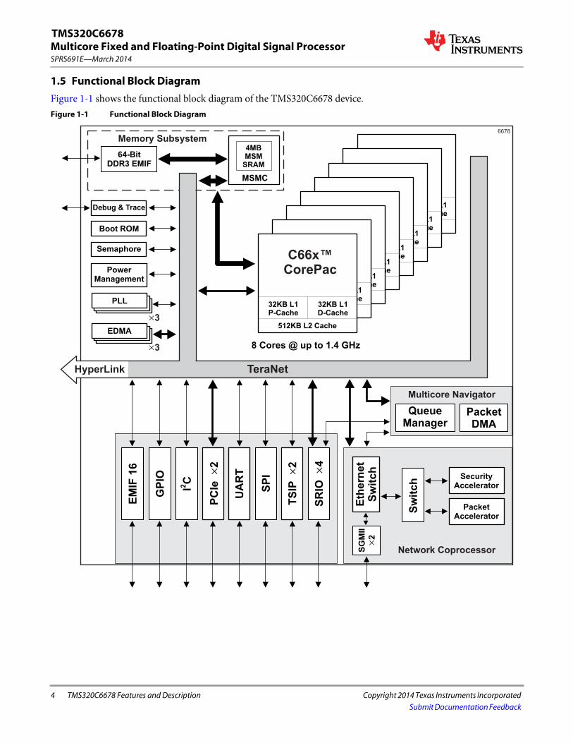
For fixed-point use, the C66x core has 4× the multiply accumulate (MAC) capability of C64x+ cores. In addition, the C66x core integrates floating point capability and the per-core raw computational performance in an industry-leading 44.8 GMACS/core and 22.4 GFLOPS/core (@1.4 GHz operating frequency). It can execute 8 single-precision floating point MAC operations per cycle and can perform double- and mixed-precision operations, and is IEEE754 compliant. The C66x core incorporates 90 new instructions (compared to the C64x+ core) targeted for floating point and vector math oriented processing. These enhancements yield sizeable performance improvements in popular DSP kernels used in signal processing, mathematical, and image acquisition functions. The C66x core is backwards code-compatible with TI's previous generation C6000 fixed and floating point DSP cores, ensuring software portability and shortened software development cycles for applications migrating to faster hardware.
The C6678 DSP integrates a large amount of on-chip memory. In addition to 32KB of L1 program and data cache, there is 512KB of dedicated memory per core that can be configured as mapped RAM or cache. The device also integrates 4096KB of Multicore Shared Memory that can be used as a shared L2 SRAM and/or shared L3 SRAM. All L2 memories incorporate error detection and error correction. For fast access to external memory, this device includes a 64-bit DDR-3 external memory interface (EMIF) running at 1600 MHz and has ECC DRAM support.
This family supports a plethora of high speed standard interfaces including RapidIO ver 2, PCI Express Gen2, and Gigabit Ethernet, as well as an integrated Ethernet switch. It also includes I2C, UART, Telecom Serial Interface Port (TSIP), and a 16-bit EMIF, along with general purpose CMOS IO. For high throughput, low latency communication between devices or with an FPGA, this device also sports a 50-Gbaud full-duplex interface called HyperLink. Adding to the network awareness of this device is a network co-processor that includes both packet and optional security acceleration. The packet accelerator can process up to 1.5 M packets/s and enables a single IP address to be used for the entire multicore C6678 device. It also provides L2 to L4 classification, along with checksum and QoS capabilities.
The C6678 device has a complete set of development tools, which includes: an enhanced C compiler, an assembly optimizer to simplify programming and scheduling, and a Windows® debugger interface for visibility into source code execution.
4 TMS320C6678 Features and Description Copyright 2014 Texas Instruments Incorporated
SPRS691E—March 2014Multicore Fixed and Floating-Point Digital Signal ProcessorTMS320C6678
Submit Documentation Feedback
1.5 Functional Block DiagramFigure 1-1 shows the functional block diagram of the TMS320C6678 device. Figure 1-1 Functional Block Diagram
8 Cores @ up to 1.4 GHz
PowerManagement
Debug & Trace
Boot ROM
Semaphore
SR
IO4
�
PC
Ie2
�
UA
RT
TS
IP�
2
SP
I
IC
2
PacketDMA
Multicore Navigator
QueueManager
GP
IO
�3
PLL
EDMA
�3
EM
IF 1
6
4MBMSM
SRAM
64-BitDDR3 EMIF
Memory Subsystem
MSMC
C66x™CorePac
32KB L1P-Cache
32KB L1D-Cache
512KB L2 Cache
C66x™CorePac
32KB L1P-Cache
32KB L1D-Cache
512KB L2 Cache
C66x™CorePac
32KB L1P-Cache
32KB L1D-Cache
512KB L2 Cache
C66x™CorePac
32KB L1P-Cache
32KB L1D-Cache
512KB L2 Cache
C66x™CorePac
32KB L1P-Cache
32KB L1D-Cache
512KB L2 Cache
C66x™CorePac
32KB L1P-Cache
32KB L1D-Cache
512KB L2 Cache
C66x™CorePac
32KB L1P-Cache
32KB L1D-Cache
512KB L2 Cache
C66x™CorePac
32KB L1P-Cache
32KB L1D-Cache
512KB L2 Cache
TeraNetHyperLink TeraNet
Network Coprocessor
Sw
itch
Eth
ern
et
Sw
itch
SG
MII
2�
PacketAccelerator
SecurityAccelerator
6678
Multicore Fixed and Floating-Point Digital Signal Processor
Copyright 2014 Texas Instruments Incorporated TMS320C6678 Features and Description 5
SPRS691E—March 2014
TMS320C6678
Submit Documentation Feedback
1.6 Release History
For detailed revision information, see ‘‘Revision History’’ on page 236.
Revision Date Description/Comments
SPRS691E March 2014 • Added 1.4-GHz support • Added GYP package support• Added DSP_SUSP_CTL register section• Updated Core Before IO Power Sequencing diagram, changing clock signal SYSCLK1P&N to REFCLK1P&N • Updated the Trace timing diagram • Updated Parameter Table Index bit field in I2C boot configuration • Updated PKTDMA_PRI_ALLOC register to be CHIP_MSIC_CTL register with new bit field added. • Updated OUTPUT_DIVIDE default value and PLL clock formula in PLL Settings section• Updated Chip Select field description in SPI boot device configuration table• Corrections applied to EMIF16 Boot Device Configuration Bit Fields • Restored Parameter Information section
SPRS691D April 2013 • Added Initial Startup row for CVDD in Recommended Operating Conditions table • Added DDR3PLLCTL1 and PASSPLLCTL1 registers to Device Status Control Registers table • Added CVDD and SmartReflex voltage parameter in SmartReflex switching table• Added HOUT timing diagram in Host Interrupt Output section • Added MPU Registers Reset Values section• Corrected PASSCLK(N/P) max cycle time from 6.4 ns to 25 ns• Corrected Reserved to be Assert local reset to all CorePacs in LRESET and NMI decoding table• Corrected PASS PLL clock to SRIOSGMIICLK in the boot device values table for Ethernet. • Updated the Timer numbering across the whole document• Updated DDR3 PLL initialization sequence
SPRS691C February 2012 • Added TeraNet connection figures and added bridge numbers to the connection tables• Changed TPCC to EDMA3CC and TPTC to EDMA3TC• Changed chip level interrupt controller name from INTC to CIC• Added the DDR3 PLL and PASS PLL Initialization Sequence• Added DEVSPEED Register section• Updated device frequency in the feature section• Corrected the SPI, DDR3, and Hyperbridge config/data memory map addresses• Restricted Output Divide of SECCTL Register to max value of divide by 2
SPRS691B August 2011 • Updated the timing and electrical sections of several peripherals • Updated the core-specific and general-purpose timer numbers • Updated the connection matrix tables in chapter 4 “System Interconnection” • Updated device boot configuration tables and figures • Updated DDR3 and PASS PLL timing figures • Removed section 7.1 “Parameter Information”
SPRS691A July 2011 • Added sections: NMI and LRSET• Added Pin Map diagrams• Added MAINPLLCTL1, DDR3PLLCTL1 and PAPLLCTL1 registers• Changed PLL diagrams of MAIN PLL, DDR3 PLL and PASS PLL• Changed C66x DSP System PLL Configuration table to include 1000 MHz and 1250 MHz columns• Corrected items in the Memory Map Summary table• Changed all occurrences of PA_SS to Network Coprocessor• Updated the complete Power-up sequencing section. RESETFULL must always de-assert after POR
SPRS691 November 2010 Initial release

6 TMS320C6678 Features and Description Copyright 2014 Texas Instruments Incorporated
SPRS691E—March 2014Multicore Fixed and Floating-Point Digital Signal ProcessorTMS320C6678
Submit Documentation Feedback

TMS320C6678SPRS691E—November 2010—Revised March 2014
Copyright 2014 Texas Instruments Incorporated Contents 7Submit Documentation Feedback
Contents
1 TMS320C6678 Features and Description . . . . . . . . . . . . .11.1 Features . . . . . . . . . . . . . . . . . . . . . . . . . . . . . . . . . . . . . . . . . . . . .11.2 Applications. . . . . . . . . . . . . . . . . . . . . . . . . . . . . . . . . . . . . . . . . .21.3 KeyStone Architecture . . . . . . . . . . . . . . . . . . . . . . . . . . . . . . . .21.4 Device Description . . . . . . . . . . . . . . . . . . . . . . . . . . . . . . . . . . .21.5 Functional Block Diagram. . . . . . . . . . . . . . . . . . . . . . . . . . . . .41.6 Release History . . . . . . . . . . . . . . . . . . . . . . . . . . . . . . . . . . . . . . .5
2 Device Overview . . . . . . . . . . . . . . . . . . . . . . . . . . . . . . . . . . 132.1 Device Characteristics . . . . . . . . . . . . . . . . . . . . . . . . . . . . . . 132.2 DSP Core Description . . . . . . . . . . . . . . . . . . . . . . . . . . . . . . . 142.3 Memory Map Summary. . . . . . . . . . . . . . . . . . . . . . . . . . . . . 172.4 Boot Sequence . . . . . . . . . . . . . . . . . . . . . . . . . . . . . . . . . . . . . 232.5 Boot Modes Supported and PLL Settings . . . . . . . . . . . . 24
2.5.1 Boot Device Field . . . . . . . . . . . . . . . . . . . . . . . . . . . . . 252.5.2 Device Configuration Field . . . . . . . . . . . . . . . . . . . . 262.5.3 Boot Parameter Table . . . . . . . . . . . . . . . . . . . . . . . . . 312.5.4 PLL Boot Configuration Settings . . . . . . . . . . . . . . . 38
2.6 Second-Level Bootloaders . . . . . . . . . . . . . . . . . . . . . . . . . . 382.7 Terminals . . . . . . . . . . . . . . . . . . . . . . . . . . . . . . . . . . . . . . . . . . 39
2.7.1 Package Terminals . . . . . . . . . . . . . . . . . . . . . . . . . . . . 392.7.2 Pin Map . . . . . . . . . . . . . . . . . . . . . . . . . . . . . . . . . . . . . . 39
2.8 Terminal Functions . . . . . . . . . . . . . . . . . . . . . . . . . . . . . . . . . 442.9 Development and Support . . . . . . . . . . . . . . . . . . . . . . . . . 70
2.9.1 Development Support . . . . . . . . . . . . . . . . . . . . . . . . 702.9.2 Device Support . . . . . . . . . . . . . . . . . . . . . . . . . . . . . . . 70
2.10 Related Documentation from Texas Instruments . . . 723 Device Configuration . . . . . . . . . . . . . . . . . . . . . . . . . . . . . . 73
3.1 Device Configuration at Device Reset . . . . . . . . . . . . . . . 733.2 Peripheral Selection After Device Reset. . . . . . . . . . . . . . 743.3 Device State Control Registers . . . . . . . . . . . . . . . . . . . . . . 74
3.3.1 Device Status Register . . . . . . . . . . . . . . . . . . . . . . . . 783.3.2 Device Configuration Register (DEVCFG). . . . . . . 793.3.3 JTAG ID Register (JTAGID) Description . . . . . . . . . 793.3.4 Kicker Mechanism Register
(KICK0 and KICK1) . . . . . . . . . . . . . . . . . . . . . . . . . . . . 803.3.5 DSP Boot Address Register
(DSP_BOOT_ADDRn) . . . . . . . . . . . . . . . . . . . . . . . . . 803.3.6 LRESETNMI PIN Status Register
(LRSTNMIPINSTAT) . . . . . . . . . . . . . . . . . . . . . . . . . . . 803.3.7 LRESETNMI PIN Status Clear Register
(LRSTNMIPINSTAT_CLR) . . . . . . . . . . . . . . . . . . . . . . 813.3.8 Reset Status Register (RESET_STAT) . . . . . . . . . . . . 833.3.9 Reset Status Clear Register
(RESET_STAT_CLR) . . . . . . . . . . . . . . . . . . . . . . . . . . . 843.3.10 Boot Complete Register
(BOOTCOMPLETE) . . . . . . . . . . . . . . . . . . . . . . . . . . . . 853.3.11 Power State Control Register
(PWRSTATECTL) . . . . . . . . . . . . . . . . . . . . . . . . . . . . . . 863.3.12 NMI Event Generation to CorePac Register
(NMIGRx). . . . . . . . . . . . . . . . . . . . . . . . . . . . . . . . . . . . . 863.3.13 IPC Generation Registers (IPCGRx) . . . . . . . . . . . . 873.3.14 IPC Acknowledgement Registers (IPCARx) . . . . 883.3.15 IPC Generation Host Register (IPCGRH) . . . . . . . 883.3.16 IPC Acknowledgement Host Register
(IPCARH) . . . . . . . . . . . . . . . . . . . . . . . . . . . . . . . . . . . . . 893.3.17 Timer Input Selection Register (TINPSEL) . . . . . 90
3.3.18 Timer Output Selection Register (TOUTPSEL) . . . . . . . . . . . . . . . . . . . . . . . . . . . . . . . . . . .93
3.3.19 Reset Mux Register (RSTMUXx). . . . . . . . . . . . . . . .943.3.20 DSP Suspension Control Register
(DSP_SUSP_CTL) . . . . . . . . . . . . . . . . . . . . . . . . . . . . . .953.3.21 Device Speed Register (DEVSPEED) . . . . . . . . . . .963.3.22 Chip Miscellaneous Control Register
(CHIP_MISC_CTL) . . . . . . . . . . . . . . . . . . . . . . . . . . . . .963.4 Pullup/Pulldown Resistors . . . . . . . . . . . . . . . . . . . . . . . . . . .97
4 System Interconnect . . . . . . . . . . . . . . . . . . . . . . . . . . . . . . . 984.1 Internal Buses and Switch Fabrics . . . . . . . . . . . . . . . . . . . .984.2 Switch Fabric Connections . . . . . . . . . . . . . . . . . . . . . . . . . .994.3 Bus Priorities . . . . . . . . . . . . . . . . . . . . . . . . . . . . . . . . . . . . . . .107
5 C66x CorePac . . . . . . . . . . . . . . . . . . . . . . . . . . . . . . . . . . . . .1085.1 Memory Architecture. . . . . . . . . . . . . . . . . . . . . . . . . . . . . . .109
5.1.1 L1P Memory. . . . . . . . . . . . . . . . . . . . . . . . . . . . . . . . . .1095.1.2 L1D Memory . . . . . . . . . . . . . . . . . . . . . . . . . . . . . . . . .1105.1.3 L2 Memory . . . . . . . . . . . . . . . . . . . . . . . . . . . . . . . . . . .1115.1.4 MSM SRAM . . . . . . . . . . . . . . . . . . . . . . . . . . . . . . . . . . .1125.1.5 L3 Memory . . . . . . . . . . . . . . . . . . . . . . . . . . . . . . . . . . .112
5.2 Memory Protection . . . . . . . . . . . . . . . . . . . . . . . . . . . . . . . .1135.3 Bandwidth Management . . . . . . . . . . . . . . . . . . . . . . . . . . .1145.4 Power-Down Control. . . . . . . . . . . . . . . . . . . . . . . . . . . . . . .1145.5 C66x CorePac Revision . . . . . . . . . . . . . . . . . . . . . . . . . . . . .1155.6 C66x CorePac Register Descriptions. . . . . . . . . . . . . . . . .115
6 Device Operating Conditions . . . . . . . . . . . . . . . . . . . . . .1166.1 Absolute Maximum Ratings . . . . . . . . . . . . . . . . . . . . . . . .1166.2 Recommended Operating Conditions . . . . . . . . . . . . . .1176.3 Electrical Characteristics . . . . . . . . . . . . . . . . . . . . . . . . . . . .1186.4 Power Supply to Peripheral I/O Mapping. . . . . . . . . . . .119
7 Peripheral Information and Electrical Specifications . . . . . . . . . . . . . . . . . . . . . . . . . . . . . . . . . . .120
7.1 Parameter Information . . . . . . . . . . . . . . . . . . . . . . . . . . . . .1207.1.1 Timing Parameters and Board Routing
Analysis . . . . . . . . . . . . . . . . . . . . . . . . . . . . . . . . . . . . .1207.1.2 1.8-V LVCMOS Signal Transition Levels . . . . . . . .120
7.2 Recommended Clock and Control Signal Transition Behavior . . . . . . . . . . . . . . . . . . . . . . . . . . . . . .120
7.3 Power Supplies . . . . . . . . . . . . . . . . . . . . . . . . . . . . . . . . . . . .1217.3.1 Power-Supply Sequencing . . . . . . . . . . . . . . . . . . . .1227.3.2 Power-Down Sequence . . . . . . . . . . . . . . . . . . . . . . .1277.3.3 Power Supply Decoupling and
Bulk Capacitors . . . . . . . . . . . . . . . . . . . . . . . . . . . . . .1277.3.4 SmartReflex . . . . . . . . . . . . . . . . . . . . . . . . . . . . . . . . . .128
7.4 Power Sleep Controller (PSC) . . . . . . . . . . . . . . . . . . . . . . .1297.4.1 Power Domains . . . . . . . . . . . . . . . . . . . . . . . . . . . . . .1297.4.2 Clock Domains . . . . . . . . . . . . . . . . . . . . . . . . . . . . . . .1307.4.3 PSC Register Memory Map . . . . . . . . . . . . . . . . . . . .131
7.5 Reset Controller . . . . . . . . . . . . . . . . . . . . . . . . . . . . . . . . . . . .1337.5.1 Power-on Reset. . . . . . . . . . . . . . . . . . . . . . . . . . . . . . .1347.5.2 Hard Reset . . . . . . . . . . . . . . . . . . . . . . . . . . . . . . . . . . .1357.5.3 Soft Reset . . . . . . . . . . . . . . . . . . . . . . . . . . . . . . . . . . . .1367.5.4 Local Reset . . . . . . . . . . . . . . . . . . . . . . . . . . . . . . . . . . .1377.5.5 Reset Priority . . . . . . . . . . . . . . . . . . . . . . . . . . . . . . . . .1377.5.6 Reset Controller Register. . . . . . . . . . . . . . . . . . . . . .1377.5.7 Reset Electrical Data / Timing . . . . . . . . . . . . . . . . .138
7.6 Main PLL and PLL Controller . . . . . . . . . . . . . . . . . . . . . . . .140

TMS320C6678SPRS691E—November 2010—Revised March 2014
8 Contents Copyright 2014 Texas Instruments Incorporated Submit Documentation Feedback
7.6.1 Main PLL Controller Device-Specific Information . . . . . . . . . . . . . . . . . . . . . . . . . . . . . . . . . 141
7.6.2 PLL Controller Memory Map. . . . . . . . . . . . . . . . . . 1437.6.3 Main PLL Control Register . . . . . . . . . . . . . . . . . . . . 1507.6.4 Main PLL and PLL Controller Initialization
Sequence . . . . . . . . . . . . . . . . . . . . . . . . . . . . . . . . . . . 1517.6.5 Main PLL Controller/SRIO/HyperLink/PCIe
Clock Input Electrical Data/Timing . . . . . . . . . . . 1517.7 DD3 PLL. . . . . . . . . . . . . . . . . . . . . . . . . . . . . . . . . . . . . . . . . . . 153
7.7.1 DDR3 PLL Control Register . . . . . . . . . . . . . . . . . . . 1537.7.2 DDR3 PLL Device-Specific Information. . . . . . . . 1547.7.3 DDR3 PLL Initialization Sequence. . . . . . . . . . . . . 1547.7.4 DDR3 PLL Input Clock Electrical
Data/Timing . . . . . . . . . . . . . . . . . . . . . . . . . . . . . . . . 1557.8 PASS PLL . . . . . . . . . . . . . . . . . . . . . . . . . . . . . . . . . . . . . . . . . . 156
7.8.1 PASS PLL Control Register . . . . . . . . . . . . . . . . . . . . 1567.8.2 PASS PLL Device-Specific Information . . . . . . . . 1577.8.3 PASS PLL Initialization Sequence . . . . . . . . . . . . . 1577.8.4 PASS PLL Input Clock Electrical
Data/Timing . . . . . . . . . . . . . . . . . . . . . . . . . . . . . . . . 1587.9 Enhanced Direct Memory Access (EDMA3)
Controller. . . . . . . . . . . . . . . . . . . . . . . . . . . . . . . . . . . . . . . 1597.9.1 EDMA3 Device-Specific Information . . . . . . . . . . 1607.9.2 EDMA3 Channel Controller Configuration . . . . 1607.9.3 EDMA3 Transfer Controller Configuration. . . . . 1607.9.4 EDMA3 Channel Synchronization Events. . . . . . 161
7.10 Interrupts . . . . . . . . . . . . . . . . . . . . . . . . . . . . . . . . . . . . . . . . 1657.10.1 Interrupt Sources and Interrupt Controller . . . 1657.10.2 CIC Registers . . . . . . . . . . . . . . . . . . . . . . . . . . . . . . . 1837.10.3 Inter-Processor Register Map. . . . . . . . . . . . . . . . 1887.10.4 NMI and LRESET . . . . . . . . . . . . . . . . . . . . . . . . . . . . 1897.10.5 External Interrupts Electrical Data/Timing . . . 1907.10.6 Host Interrupt Output. . . . . . . . . . . . . . . . . . . . . . . 191
7.11 Memory Protection Unit (MPU) . . . . . . . . . . . . . . . . . . . 1927.11.1 MPU Registers . . . . . . . . . . . . . . . . . . . . . . . . . . . . . . 1957.11.2 MPU Programmable Range Registers . . . . . . . . 200
7.12 DDR3 Memory Controller . . . . . . . . . . . . . . . . . . . . . . . . . 2057.12.1 DDR3 Memory Controller Device-Specific
Information . . . . . . . . . . . . . . . . . . . . . . . . . . . . . . . . . 205
7.12.2 DDR3 Memory Controller Race Condition Consideration. . . . . . . . . . . . . . . . . . . . . . . . . . . . . . . .205
7.12.3 DDR3 Memory Controller Electrical Data/Timing . . . . . . . . . . . . . . . . . . . . . . . . . . . . . . . . .206
7.13 I2C Peripheral . . . . . . . . . . . . . . . . . . . . . . . . . . . . . . . . . . . . .2077.13.1 I2C Device-Specific Information . . . . . . . . . . . . . .2077.13.2 I2C Peripheral Register Description(s) . . . . . . . .2087.13.3 I2C Electrical Data/Timing. . . . . . . . . . . . . . . . . . . .209
7.14 SPI Peripheral . . . . . . . . . . . . . . . . . . . . . . . . . . . . . . . . . . . . .2127.14.1 SPI Electrical Data/Timing. . . . . . . . . . . . . . . . . . . .212
7.15 HyperLink Peripheral. . . . . . . . . . . . . . . . . . . . . . . . . . . . . .2157.15.1 HyperLink Device-Specific Interrupt Event. . . .2157.15.2 HyperLink Electrical Data/Timing . . . . . . . . . . . .217
7.16 UART Peripheral . . . . . . . . . . . . . . . . . . . . . . . . . . . . . . . . . .2197.17 PCIe Peripheral . . . . . . . . . . . . . . . . . . . . . . . . . . . . . . . . . . .2207.18 TSIP Peripheral. . . . . . . . . . . . . . . . . . . . . . . . . . . . . . . . . . . .221
7.18.1 TSIP Electrical Data/Timing . . . . . . . . . . . . . . . . . .2217.19 EMIF16 Peripheral. . . . . . . . . . . . . . . . . . . . . . . . . . . . . . . . .223
7.19.1 EMIF16 Electrical Data/Timing . . . . . . . . . . . . . . .2237.20 Packet Accelerator . . . . . . . . . . . . . . . . . . . . . . . . . . . . . . . .2257.21 Security Accelerator. . . . . . . . . . . . . . . . . . . . . . . . . . . . . . .2257.22 Gigabit Ethernet (GbE) Switch Subsystem. . . . . . . . . .2267.23 Management Data Input/Output (MDIO) . . . . . . . . . .2287.24 Timers . . . . . . . . . . . . . . . . . . . . . . . . . . . . . . . . . . . . . . . . . . . .229
7.24.1 Timers Device-Specific Information . . . . . . . . . .2297.24.2 Timers Electrical Data/Timing . . . . . . . . . . . . . . . .230
7.25 Serial RapidIO (SRIO) Port . . . . . . . . . . . . . . . . . . . . . . . . .2307.26 General-Purpose Input/Output (GPIO) . . . . . . . . . . . . .231
7.26.1 GPIO Device-Specific Information . . . . . . . . . . . .2317.26.2 GPIO Electrical Data/Timing. . . . . . . . . . . . . . . . . .231
7.27 Semaphore2 . . . . . . . . . . . . . . . . . . . . . . . . . . . . . . . . . . . . . .2327.28 Emulation Features and Capability . . . . . . . . . . . . . . . .232
7.28.1 Advanced Event Triggering (AET) . . . . . . . . . . . .2327.28.2 Trace. . . . . . . . . . . . . . . . . . . . . . . . . . . . . . . . . . . . . . . .2337.28.3 IEEE 1149.1 JTAG . . . . . . . . . . . . . . . . . . . . . . . . . . . .234
8 Revision History . . . . . . . . . . . . . . . . . . . . . . . . . . . . . . . . . . .2369 Mechanical Data . . . . . . . . . . . . . . . . . . . . . . . . . . . . . . . . . .241
9.1 Thermal Data . . . . . . . . . . . . . . . . . . . . . . . . . . . . . . . . . . . . . .2419.2 Packaging Information . . . . . . . . . . . . . . . . . . . . . . . . . . . . .241

TMS320C6678SPRS691E—November 2010—Revised March 2014
Copyright 2014 Texas Instruments Incorporated List of Figures 9Submit Documentation Feedback
List of Figures
Figure 1-1 Functional Block Diagram . . . . . . . . . . . . . . . . . . . . . . .4Figure 2-1 DSP Core Data Paths . . . . . . . . . . . . . . . . . . . . . . . . . . 16Figure 2-2 Boot Mode Pin Decoding . . . . . . . . . . . . . . . . . . . . . . 24Figure 2-3 No Boot/ EMIF16 Configuration Fields. . . . . . . . . . 26Figure 2-4 Serial Rapid I/O Device Configuration Fields . . . . 26Figure 2-5 Ethernet (SGMII) Device Configuration Fields . . . 27Figure 2-6 PCI Device Configuration Fields. . . . . . . . . . . . . . . . 27Figure 2-7 I2C Master Mode Device Configuration
Bit Fields . . . . . . . . . . . . . . . . . . . . . . . . . . . . . . . . . . . . . . 28Figure 2-8 I2C Passive Mode Device Configuration
Bit Fields . . . . . . . . . . . . . . . . . . . . . . . . . . . . . . . . . . . . . . 29Figure 2-9 SPI Device Configuration Bit Fields . . . . . . . . . . . . . 29Figure 2-10 HyperLink Boot Device Configuration Fields. . . . 30Figure 2-11 CYP 841-Pin BGA Package (Bottom View). . . . . . . 39Figure 2-12 Pin Map Quadrants (Bottom View) . . . . . . . . . . . . . 39Figure 2-13 Upper Left Quadrant—A (Bottom View). . . . . . . . 40Figure 2-14 Upper Right Quadrant—B (Bottom View) . . . . . . 41Figure 2-15 Lower Right Quadrant—C (Bottom View) . . . . . . 42Figure 2-16 Lower Left Quadrant—D (Bottom View). . . . . . . . 43Figure 2-17 C66x DSP Device Nomenclature (including
the TMS320C6678) . . . . . . . . . . . . . . . . . . . . . . . . . . . . 71Figure 3-1 Device Status Register . . . . . . . . . . . . . . . . . . . . . . . . . 78Figure 3-2 Device Configuration Register (DEVCFG) . . . . . . . 79Figure 3-3 JTAG ID Register (JTAGID) . . . . . . . . . . . . . . . . . . . . . 79Figure 3-4 DSP BOOT Address Register
(DSP_BOOT_ADDRn) . . . . . . . . . . . . . . . . . . . . . . . . . . 80Figure 3-5 LRESETNMI PIN Status Register
(LRSTNMIPINSTAT) . . . . . . . . . . . . . . . . . . . . . . . . . . . . 80Figure 3-6 LRESETNMI PIN Status Clear Register
(LRSTNMIPINSTAT_CLR) . . . . . . . . . . . . . . . . . . . . . . . 81Figure 3-7 Reset Status Register (RESET_STAT) . . . . . . . . . . . . 83Figure 3-8 Reset Status Clear Register (RESET_STAT_CLR). . 84Figure 3-9 Boot Complete Register (BOOTCOMPLETE) . . . . . 85Figure 3-10 Power State Control Register (PWRSTATECTL) . . 86Figure 3-11 NMI Generation Register (NMIGRx). . . . . . . . . . . . . 86Figure 3-12 IPC Generation (IPCGRx) Registers . . . . . . . . . . . . . 87Figure 3-13 IPC Acknowledgement (IPCARx) Registers. . . . . . 88Figure 3-14 IPC Generation (IPCGRH) Registers . . . . . . . . . . . . . 88Figure 3-15 IPC Acknowledgement Register (IPCARH) . . . . . . 89Figure 3-16 Timer Input Selection Register (TINPSEL) . . . . . . . 90Figure 3-17 Timer Output Selection Register
(TOUTPSEL) . . . . . . . . . . . . . . . . . . . . . . . . . . . . . . . . . . . 93Figure 3-18 Reset Mux Register (RSTMUXx). . . . . . . . . . . . . . . . . 94Figure 3-19 DSP Suspension Control Register
(DSP_SUSP_CTL) . . . . . . . . . . . . . . . . . . . . . . . . . . . . . . 95Figure 3-20 Device Speed Register (DEVSPEED) . . . . . . . . . . . . 96Figure 3-21 Chip Miscellaneous Control Register
(CHIP_MISC_CTL). . . . . . . . . . . . . . . . . . . . . . . . . . . . . . 96Figure 4-1 TeraNet 2A for C6678. . . . . . . . . . . . . . . . . . . . . . . . . . 99Figure 4-2 TeraNet 3A for C6678. . . . . . . . . . . . . . . . . . . . . . . . . 100Figure 4-3 TeraNet 3P_A & B for C6678 . . . . . . . . . . . . . . . . . . 102Figure 4-4 TeraNet 6P_B and 3P_Tracer for C6678. . . . . . . . 103Figure 5-1 C66x CorePac Block Diagram . . . . . . . . . . . . . . . . . 108
Figure 5-2 L1P Memory Configurations . . . . . . . . . . . . . . . . . . .109Figure 5-3 L1D Memory Configurations . . . . . . . . . . . . . . . . . .110Figure 5-4 L2 Memory Configurations . . . . . . . . . . . . . . . . . . . .111Figure 5-5 CorePac Revision ID Register (MM_REVID)
Address - 0181 2000h . . . . . . . . . . . . . . . . . . . . . . . . .115Figure 7-1 Input and Output Voltage Reference
Levels for AC Timing Measurements . . . . . . . . . . .120Figure 7-2 Rise and Fall Transition Time Voltage
Reference Levels . . . . . . . . . . . . . . . . . . . . . . . . . . . . .120Figure 7-3 Core Before IO Power Sequencing . . . . . . . . . . . .123Figure 7-4 IO Before Core Power Sequencing . . . . . . . . . . . .125Figure 7-5 SmartReflex 4-Pin VID Interface Timing . . . . . . . .128Figure 7-6 RESETFULL Reset Timing . . . . . . . . . . . . . . . . . . . . . .138Figure 7-7 Soft/Hard-Reset Timing . . . . . . . . . . . . . . . . . . . . . . .138Figure 7-8 Boot Configuration Timing . . . . . . . . . . . . . . . . . . . .139Figure 7-9 Main PLL and PLL Controller . . . . . . . . . . . . . . . . . .140Figure 7-10 PLL Secondary Control Register (SECCTL)) . . . . .144Figure 7-11 PLL Controller Divider Register (PLLDIVn) . . . . . .145Figure 7-12 PLL Controller Clock Align Control Register
(ALNCTL) . . . . . . . . . . . . . . . . . . . . . . . . . . . . . . . . . . . . .145Figure 7-13 PLLDIV Divider Ratio Change Status Register
(DCHANGE) . . . . . . . . . . . . . . . . . . . . . . . . . . . . . . . . . . .146Figure 7-14 SYSCLK Status Register (SYSTAT) . . . . . . . . . . . . . .146Figure 7-15 Reset Type Status Register (RSTYPE) . . . . . . . . . . .147Figure 7-16 Reset Control Register (RSTCTRL) . . . . . . . . . . . . . .148Figure 7-17 Reset Configuration Register (RSTCFG). . . . . . . . .148Figure 7-18 Reset Isolation Register (RSISO) . . . . . . . . . . . . . . . .149Figure 7-19 Main PLL Control Register 0 (MAINPLLCTL0) . . .150Figure 7-20 Main PLL Control Register 1 (MAINPLLCTL1) . . .150Figure 7-21 Main PLL Controller/SRIO/HyperLink/PCIe
Clock Input Timing. . . . . . . . . . . . . . . . . . . . . . . . . . . .152Figure 7-22 Main PLL Clock Input Transition Time . . . . . . . . .152Figure 7-23 DDR3 PLL Block Diagram . . . . . . . . . . . . . . . . . . . . . .153Figure 7-24 DDR3 PLL Control Register 0 (DDR3PLLCTL0). . .153Figure 7-25 DDR3 PLL Control Register 1 (DDR3PLLCTL1). . .154Figure 7-26 DDR3 PLL DDRCLK Timing. . . . . . . . . . . . . . . . . . . . .155Figure 7-27 PASS PLL Block Diagram . . . . . . . . . . . . . . . . . . . . . .156Figure 7-28 PASS PLL Control Register 0 (PASSPLLCTL0) . . . .156Figure 7-29 PASS PLL Control Register 1 (PASSPLLCTL1) . . . .157Figure 7-30 PASS PLL Timing . . . . . . . . . . . . . . . . . . . . . . . . . . . . . .158Figure 7-31 TMS320C6678 Interrupt Topology . . . . . . . . . . . . .166Figure 7-32 TMS320C6678 System Event Inputs —
C66x CorePac Primary Interrupts . . . . . . . . . . . . . .167Figure 7-33 NMI and Local Reset Timing . . . . . . . . . . . . . . . . . . .190Figure 7-34 HOUT Timing . . . . . . . . . . . . . . . . . . . . . . . . . . . . . . . . .191Figure 7-35 Configuration Register (CONFIG) . . . . . . . . . . . . . .199Figure 7-36 Programmable Range n Start Address
Register (PROGn_MPSAR) . . . . . . . . . . . . . . . . . . . . .200Figure 7-37 Programmable Range n End Address
Register (PROGn_MPEAR) . . . . . . . . . . . . . . . . . . . . .200Figure 7-38 Programmable Range n Memory Protection
Page Attribute Register (PROGn_MPPA) . . . . . . .201Figure 7-39 I2C Module Block Diagram. . . . . . . . . . . . . . . . . . . . .208Figure 7-40 I2C Receive Timings . . . . . . . . . . . . . . . . . . . . . . . . . . .210

TMS320C6678SPRS691E—November 2010—Revised March 2014
10 List of Figures Copyright 2014 Texas Instruments Incorporated Submit Documentation Feedback
Figure 7-41 I2C Transmit Timings . . . . . . . . . . . . . . . . . . . . . . . . . 211Figure 7-42 SPI Master Mode Timing Diagrams —
Base Timings for 3 Pin Mode . . . . . . . . . . . . . . . . . . 214Figure 7-43 SPI Additional Timings for 4 Pin Master
Mode with Chip Select Option . . . . . . . . . . . . . . . . 214Figure 7-44 HyperLink Station Management Clock
Timing . . . . . . . . . . . . . . . . . . . . . . . . . . . . . . . . . . . . . . . 218Figure 7-45 HyperLink Station Management Transmit
Timing . . . . . . . . . . . . . . . . . . . . . . . . . . . . . . . . . . . . . . . 218Figure 7-46 HyperLink Station Management Receive
Timing . . . . . . . . . . . . . . . . . . . . . . . . . . . . . . . . . . . . . . . 218Figure 7-47 UART Receive Timing Waveform . . . . . . . . . . . . . . 219Figure 7-48 UART CTS (Clear-to-Send Input) —
Autoflow Timing Waveform . . . . . . . . . . . . . . . . . . 219Figure 7-49 UART Transmit Timing Waveform . . . . . . . . . . . . . 220Figure 7-50 UART RTS (Request-to-Send Output) —
Autoflow Timing Waveform . . . . . . . . . . . . . . . . . . 220
Figure 7-51 TSIP 2x Timing Diagram(1) . . . . . . . . . . . . . . . . . . . . .221Figure 7-52 TSIP 1x Timing Diagram(1) . . . . . . . . . . . . . . . . . . . . .222Figure 7-53 EMIF16 Asynchronous Memory Read
Timing Diagram . . . . . . . . . . . . . . . . . . . . . . . . . . . . . .224Figure 7-54 EMIF16 Asynchronous Memory Write
Timing Diagram . . . . . . . . . . . . . . . . . . . . . . . . . . . . . .224Figure 7-55 EMIF16 EM_WAIT Read Timing Diagram . . . . . . .225Figure 7-56 EMIF16 EM_WAIT Write Timing Diagram . . . . . . .225Figure 7-57 MACID1 Register . . . . . . . . . . . . . . . . . . . . . . . . . . . . . .226Figure 7-58 MACID2 Register . . . . . . . . . . . . . . . . . . . . . . . . . . . . . .226Figure 7-59 CPTS_RFTCLK_SEL Register. . . . . . . . . . . . . . . . . . . .227Figure 7-60 MDIO Input Timing . . . . . . . . . . . . . . . . . . . . . . . . . . .228Figure 7-61 MDIO Output Timing. . . . . . . . . . . . . . . . . . . . . . . . . .228Figure 7-62 Timer Timing . . . . . . . . . . . . . . . . . . . . . . . . . . . . . . . . .230Figure 7-63 GPIO Timing . . . . . . . . . . . . . . . . . . . . . . . . . . . . . . . . . .231Figure 7-64 Trace Timing . . . . . . . . . . . . . . . . . . . . . . . . . . . . . . . . .233Figure 7-65 JTAG Test-Port Timing . . . . . . . . . . . . . . . . . . . . . . . .235

TMS320C6678SPRS691E—November 2010—Revised March 2014
Copyright 2014 Texas Instruments Incorporated List of Tables 11Submit Documentation Feedback
List of Tables
Table 2-1 Device Characteristics . . . . . . . . . . . . . . . . . . . . . . . . . 13Table 2-2 Memory Map Summary. . . . . . . . . . . . . . . . . . . . . . . . 17Table 2-3 Bootloader section in L2 SRAM . . . . . . . . . . . . . . . . 23Table 2-4 Boot Mode Pins: Boot Device Values . . . . . . . . . . . 25Table 2-5 Extended Boot Modes . . . . . . . . . . . . . . . . . . . . . . . . . 25Table 2-6 No Boot / EMIF16 Configuration
Field Descriptions . . . . . . . . . . . . . . . . . . . . . . . . . . . . . 26Table 2-7 Serial Rapid I/O Configuration
Field Descriptions . . . . . . . . . . . . . . . . . . . . . . . . . . . . . 26Table 2-8 Ethernet (SGMII) Configuration
Field Descriptions . . . . . . . . . . . . . . . . . . . . . . . . . . . . . 27Table 2-9 PCI Device Configuration Field Descriptions. . . . 27Table 2-10 BAR Config / PCIe Window Sizes . . . . . . . . . . . . . . . 28Table 2-11 I2C Master Mode Device Configuration
Field Descriptions . . . . . . . . . . . . . . . . . . . . . . . . . . . . . 28Table 2-12 I2C Passive Mode Device Configuration
Field Descriptions . . . . . . . . . . . . . . . . . . . . . . . . . . . . . 29Table 2-13 SPI Device Configuration Field Descriptions . . . . 29Table 2-14 HyperLink Boot Device Configuration
Field Descriptions . . . . . . . . . . . . . . . . . . . . . . . . . . . . . 30Table 2-15 Boot Parameter Table Common Parameters . . . . 31Table 2-16 EMIF16 Boot Mode Parameter Table . . . . . . . . . . . 31Table 2-17 SRIO Boot Mode Parameter Table . . . . . . . . . . . . . . 32Table 2-18 Ethernet Boot Mode Parameter Table . . . . . . . . . . 32Table 2-19 PCIe Boot Mode Parameter Table . . . . . . . . . . . . . . 34Table 2-20 I2C Boot Mode Parameter Table. . . . . . . . . . . . . . . . 34Table 2-21 SPI Boot Mode Parameter Table. . . . . . . . . . . . . . . . 35Table 2-22 HyperLink Boot Mode Parameter Table . . . . . . . . 36Table 2-23 DDR3 Boot Parameter Table . . . . . . . . . . . . . . . . . . . 37Table 2-24 C66x DSP System PLL Configuration . . . . . . . . . . . 38Table 2-25 I/O Functional Symbol Definitions . . . . . . . . . . . . . 44Table 2-26 Terminal Functions — Signals and Control
by Function . . . . . . . . . . . . . . . . . . . . . . . . . . . . . . . . . . . 44Table 2-27 Terminal Functions — Power and Ground. . . . . . 57Table 2-28 Terminal Functions — By Signal Name . . . . . . . . . 58Table 2-29 Terminal Functions — By Ball Number . . . . . . . . . 63Table 3-1 TMS320C6678 Device Configuration Pins . . . . . . 73Table 3-2 Device State Control Registers . . . . . . . . . . . . . . . . . 74Table 3-3 Device Status Register Field Descriptions. . . . . . . 78Table 3-4 Device Configuration Register (DEVCFG)
Field Descriptions . . . . . . . . . . . . . . . . . . . . . . . . . . . . . 79Table 3-5 JTAG ID Register (JTAGID) Field Descriptions . . . 79Table 3-6 DSP BOOT Address Register
(DSP_BOOT_ADDRn) Field Descriptions . . . . . . . . 80Table 3-7 LRESETNMI PIN Status Register
(LRSTNMIPINSTAT) Field Descriptions . . . . . . . . . . 81Table 3-8 LRESETNMI PIN Status Clear Register
(LRSTNMIPINSTAT_CLR) Field Descriptions . . . . . 81Table 3-9 Reset Status Register (RESET_STAT) Field
Descriptions . . . . . . . . . . . . . . . . . . . . . . . . . . . . . . . . . . 83Table 3-10 Reset Status Clear Register
(RESET_STAT_CLR) Field Descriptions . . . . . . . . . . 84Table 3-11 Boot Complete Register (BOOTCOMPLETE)
Field Descriptions . . . . . . . . . . . . . . . . . . . . . . . . . . . . . 85
Table 3-12 Power State Control Register (PWRSTATECTL) Field Descriptions . . . . . . . . . . . . . . . . . . . . . . . . . . . . . .86
Table 3-13 NMI Generation Register (NMIGRx) Field Descriptions . . . . . . . . . . . . . . . . . . . . . . . . . . . . . .87
Table 3-14 IPC Generation Registers (IPCGRx) Field Descriptions . . . . . . . . . . . . . . . . . . . . . . . . . . . . . .87
Table 3-15 IPC Acknowledgement Registers (IPCARx) Field Descriptions . . . . . . . . . . . . . . . . . . . . . . . . . . . . . .88
Table 3-16 IPC Generation Registers (IPCGRH) Field Descriptions . . . . . . . . . . . . . . . . . . . . . . . . . . . . . .89
Table 3-17 IPC Acknowledgement Register (IPCARH) Field Descriptions . . . . . . . . . . . . . . . . . . . . . . . . . . . . . .89
Table 3-18 Timer Input Selection Field Description (TINPSEL) . . . . . . . . . . . . . . . . . . . . . . . . . . . . . . . . . . . . . .90
Table 3-19 Timer Output Selection Register (TOUTPSEL) Field Description. . . . . . . . . . . . . . . . . . . . . . . . . . . . . . .93
Table 3-20 Reset Mux Register (RSTMUXx) Field Descriptions . . . . . . . . . . . . . . . . . . . . . . . . . . . . . .94
Table 3-21 DSP Suspension Control Register (DSP_SUSP_CTL) Field Descriptions. . . . . . . . . . . . .95
Table 3-22 Device Speed Register (DEVSPEED) Field Descriptions . . . . . . . . . . . . . . . . . . . . . . . . . . . . . .96
Table 3-23 Chip Miscellaneous Control Register (CHIP_MISC_CTL) Field Descriptions . . . . . . . . . . . .96
Table 4-1 Switch Fabric Connection Matrix Section 1. . . . .101Table 4-2 Switch Fabric Connection Matrix Section 2. . . . .104Table 4-3 Switch Fabric Connection Matrix Section 3. . . . .105Table 5-1 Available Memory Page Protection Schemes . . .113Table 5-2 CorePac Revision ID Register (MM_REVID)
Field Descriptions . . . . . . . . . . . . . . . . . . . . . . . . . . . . .115Table 6-1 Absolute Maximum Ratings . . . . . . . . . . . . . . . . . . .116Table 6-2 Recommended Operating Conditions . . . . . . . . .117Table 6-3 Electrical Characteristics. . . . . . . . . . . . . . . . . . . . . . .118Table 6-4 Power Supply to Peripheral I/O Mapping . . . . . .119Table 7-1 Power Supply Rails on the TMS320C6678 . . . . . .121Table 7-2 Core Before IO Power Sequencing . . . . . . . . . . . . .124Table 7-3 IO Before Core Power Sequencing . . . . . . . . . . . . .126Table 7-4 Clock Sequencing. . . . . . . . . . . . . . . . . . . . . . . . . . . . .127Table 7-5 SmartReflex 4-Pin VID Interface Switching
Characteristics . . . . . . . . . . . . . . . . . . . . . . . . . . . . . . . .128Table 7-6 Power Domains . . . . . . . . . . . . . . . . . . . . . . . . . . . . . . .129Table 7-7 Clock Domains. . . . . . . . . . . . . . . . . . . . . . . . . . . . . . . .130Table 7-8 PSC Register Memory Map . . . . . . . . . . . . . . . . . . . .131Table 7-9 Reset Types . . . . . . . . . . . . . . . . . . . . . . . . . . . . . . . . . . .133Table 7-10 Reset Timing Requirements . . . . . . . . . . . . . . . . . . .138Table 7-11 Reset Switching Characteristics Over
Recommended Operating Conditions . . . . . . . . .138Table 7-12 Boot Configuration Timing Requirements. . . . . .139Table 7-13 Main PLL Stabilization, Lock, and Reset Times . .142Table 7-14 PLL Controller Registers (Including Reset
Controller) . . . . . . . . . . . . . . . . . . . . . . . . . . . . . . . . . . . .143Table 7-15 PLL Secondary Control Register (SECCTL)
Field Descriptions . . . . . . . . . . . . . . . . . . . . . . . . . . . . .144
TMS320C6678SPRS691E—November 2010—Revised March 2014
12 List of Tables Copyright 2014 Texas Instruments Incorporated Submit Documentation Feedback
Table 7-16 PLL Controller Divider Register (PLLDIVn) Field Descriptions . . . . . . . . . . . . . . . . . . . . . . . . . . . . 145
Table 7-17 PLL Controller Clock Align Control Register (ALNCTL) Field Descriptions . . . . . . . . . . . . . . . . . . 146
Table 7-18 PLLDIV Divider Ratio Change Status Register (DCHANGE) Field Descriptions . . . . . . . . . . . . . . . . 146
Table 7-19 SYSCLK Status Register (SYSTAT) Field Descriptions . . . . . . . . . . . . . . . . . . . . . . . . . . . . 147
Table 7-20 Reset Type Status Register (RSTYPE) Field Descriptions . . . . . . . . . . . . . . . . . . . . . . . . . . . . 147
Table 7-21 Reset Control Register (RSTCTRL) Field Descriptions . . . . . . . . . . . . . . . . . . . . . . . . . . . . 148
Table 7-22 Reset Configuration Register (RSTCFG) Field Descriptions . . . . . . . . . . . . . . . . . . . . . . . . . . . . 148
Table 7-23 Reset Isolation Register (RSISO) Field Descriptions . . . . . . . . . . . . . . . . . . . . . . . . . . . . 149
Table 7-24 Main PLL Control Register 0 (MAINPLLCTL0) Field Descriptions . . . . . . . . . . . . . . . . . . . . . . . . . . . . 150
Table 7-25 Main PLL Control Register 1 (MAINPLLCTL1) Field Descriptions . . . . . . . . . . . . . . . . . . . . . . . . . . . . 150
Table 7-26 Main PLL Controller/SRIO/HyperLink/PCIe Clock Input Timing Requirements. . . . . . . . . . . . . 151
Table 7-27 DDR3 PLL Control Register 0 Field Descriptions . . . . . . . . . . . . . . . . . . . . . . . . . . . . 153
Table 7-28 DDR3 PLL Control Register 1 Field Descriptions . . . . . . . . . . . . . . . . . . . . . . . . . . . . 154
Table 7-29 DDR3 PLL DDRSYSCLK1(N|P) Timing Requirements . . . . . . . . . . . . . . . . . . . . . . . . 155
Table 7-30 PASS PLL Control Register 0 Field Descriptions . . . . . . . . . . . . . . . . . . . . . . . . . . . . 157
Table 7-31 PASS PLL Control Register 1 Field Descriptions . . . . . . . . . . . . . . . . . . . . . . . . . . . . 157
Table 7-32 PASS PLL Timing Requirements . . . . . . . . . . . . . . . 158Table 7-33 EDMA3 Channel Controller Configuration . . . . . 160Table 7-34 EDMA3 Transfer Controller Configuration . . . . . 161Table 7-35 EDMA3CC0 Events for C6678 . . . . . . . . . . . . . . . . . 161Table 7-36 EDMA3CC1 Events for C6678 . . . . . . . . . . . . . . . . . 161Table 7-37 EDMA3CC2 Events for C6678 . . . . . . . . . . . . . . . . . 163Table 7-38 CIC0 Event Inputs (Secondary Interrupts
for C66x CorePacs) . . . . . . . . . . . . . . . . . . . . . . . . . . . 170Table 7-39 CIC1 Event Inputs (Secondary Interrupts
for C66x CorePacs) . . . . . . . . . . . . . . . . . . . . . . . . . . . 174Table 7-40 CIC2 Event Inputs (Secondary Events for
EDMA3CC1 and EDMA3CC2). . . . . . . . . . . . . . . . . . 178Table 7-41 CIC3 Event Inputs (Secondary Events for
EDMA3CC0 and HyperLink) . . . . . . . . . . . . . . . . . . . 181Table 7-42 CIC0/CIC1 Register . . . . . . . . . . . . . . . . . . . . . . . . . . . 183Table 7-43 CIC2 Register. . . . . . . . . . . . . . . . . . . . . . . . . . . . . . . . . 185Table 7-44 CIC3 Register. . . . . . . . . . . . . . . . . . . . . . . . . . . . . . . . . 187Table 7-45 IPC Generation Registers (IPCGRx) . . . . . . . . . . . . 188Table 7-46 LRESET and NMI Decoding. . . . . . . . . . . . . . . . . . . . 189Table 7-47 NMI and Local Reset Timing Requirements . . . . 190Table 7-48 HOUT Switching Characteristics . . . . . . . . . . . . . . 191Table 7-49 MPU Default Configuration . . . . . . . . . . . . . . . . . . . 192Table 7-50 MPU Memory Regions . . . . . . . . . . . . . . . . . . . . . . . . 192Table 7-51 Privilege ID Settings . . . . . . . . . . . . . . . . . . . . . . . . . . 192
Table 7-52 Master ID Settings . . . . . . . . . . . . . . . . . . . . . . . . . . .193Table 7-53 MPU0 Registers . . . . . . . . . . . . . . . . . . . . . . . . . . . . . . .195Table 7-54 MPU1 Registers . . . . . . . . . . . . . . . . . . . . . . . . . . . . . . .196Table 7-55 MPU2 Registers . . . . . . . . . . . . . . . . . . . . . . . . . . . . . . .197Table 7-56 MPU3 Registers . . . . . . . . . . . . . . . . . . . . . . . . . . . . . . .198Table 7-57 Configuration Register (CONFIG)
Field Descriptions . . . . . . . . . . . . . . . . . . . . . . . . . . . . .199Table 7-58 Programmable Range n Start Address Register
(PROGn_MPSAR) Field Descriptions. . . . . . . . . . . .200Table 7-59 Programmable Range n End Address Register
(PROGn_MPEAR) Field Descriptions. . . . . . . . . . . .200Table 7-60 Programmable Range n Memory Protection
Page Attribute Register (PROGn_MPPA) Field Descriptions . . . . . . . . . . . . . . . . . . . . . . . . . . . . .201
Table 7-61 Programmable Range n Registers Reset Values for MPU0 . . . . . . . . . . . . . . . . . . . . . . . . . . . . . .203
Table 7-62 Programmable Range n Registers Reset Values for MPU1 . . . . . . . . . . . . . . . . . . . . . . . . . . . . . .203
Table 7-63 Programmable Range n Registers Reset Values for MPU2 . . . . . . . . . . . . . . . . . . . . . . . . . . . . . .204
Table 7-64 Programmable Range n Registers Reset Values for MPU3 . . . . . . . . . . . . . . . . . . . . . . . . . . . . . .204
Table 7-65 I2C Registers . . . . . . . . . . . . . . . . . . . . . . . . . . . . . . . . . .208Table 7-66 I2C Timing Requirements. . . . . . . . . . . . . . . . . . . . . .209Table 7-67 I2C Switching Characteristics . . . . . . . . . . . . . . . . . .210Table 7-68 SPI Timing Requirements. . . . . . . . . . . . . . . . . . . . . .212Table 7-69 SPI Switching Characteristics . . . . . . . . . . . . . . . . . .212Table 7-70 HyperLink Events for C6678 . . . . . . . . . . . . . . . . . . .215Table 7-71 HyperLink Peripheral Timing
Requirements. . . . . . . . . . . . . . . . . . . . . . . . . . . . . . . . .217Table 7-72 HyperLink Peripheral Switching
Characteristics . . . . . . . . . . . . . . . . . . . . . . . . . . . . . . . .217Table 7-73 UART Timing Requirements . . . . . . . . . . . . . . . . . . .219Table 7-74 UART Switching Characteristics. . . . . . . . . . . . . . . .220Table 7-75 Timing Requirements for TSIP 2x Mode . . . . . . . .221Table 7-76 Timing Requirements for TSIP 1x Mode . . . . . . . .222Table 7-77 EMIF16 Asynchronous Memory Timing
Requirements. . . . . . . . . . . . . . . . . . . . . . . . . . . . . . . . .223Table 7-78 MACID1 Register Field Descriptions. . . . . . . . . . . .226Table 7-79 MACID2 Register Field Descriptions. . . . . . . . . . . .226Table 7-80 CPTS_RFTCLK_SEL Register
Field Descriptions . . . . . . . . . . . . . . . . . . . . . . . . . . . . .227Table 7-81 MDIO Timing Requirements . . . . . . . . . . . . . . . . . . .228Table 7-82 MDIO Switching Characteristics . . . . . . . . . . . . . . .228Table 7-83 Timer Input Timing Requirements . . . . . . . . . . . . .230Table 7-84 Timer Output Switching Characteristics. . . . . . . .230Table 7-85 GPIO Input Timing Requirements . . . . . . . . . . . . . .231Table 7-86 GPIO Output Switching Characteristics . . . . . . . .231Table 7-87 DSP Trace Switching Characteristics . . . . . . . . . . .233Table 7-88 STM Trace Switching Characteristics . . . . . . . . . .233Table 7-89 JTAG Test Port Timing Requirements . . . . . . . . . .234Table 7-90 JTAG Test Port Switching Characteristics . . . . . . .234Table 9-1 Thermal Resistance Characteristics for
CYP (PBGA 841-Pin Package) . . . . . . . . . . . . . . . . . .241Table 9-2 Thermal Resistance Characteristics for
GYP (PBGA 841-Pin Package) . . . . . . . . . . . . . . . . . .241
Multicore Fixed and Floating-Point Digital Signal Processor
Copyright 2014 Texas Instruments Incorporated Device Overview 13
SPRS691E—March 2014
TMS320C6678
Submit Documentation Feedback
2 Device Overview
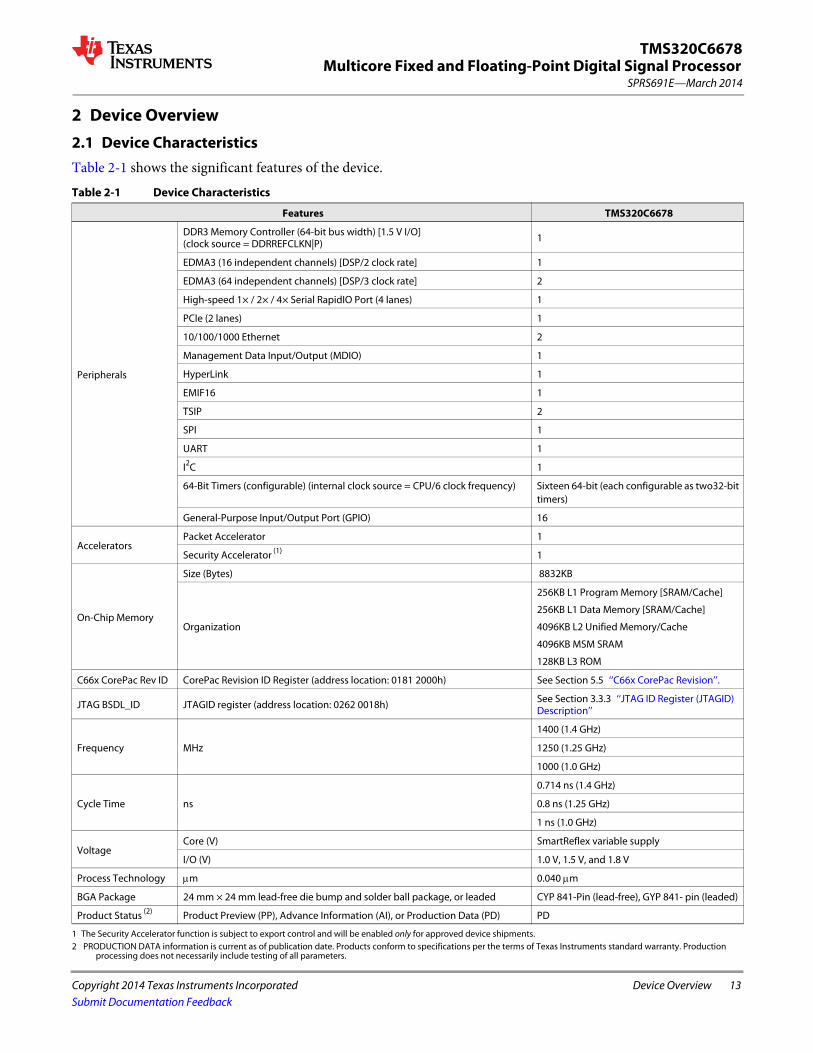
2.1 Device Characteristics Table 2-1 shows the significant features of the device.Table 2-1 Device Characteristics
Features TMS320C6678
Peripherals
DDR3 Memory Controller (64-bit bus width) [1.5 V I/O] (clock source = DDRREFCLKN|P) 1
EDMA3 (16 independent channels) [DSP/2 clock rate] 1
EDMA3 (64 independent channels) [DSP/3 clock rate] 2
High-speed 1× / 2× / 4× Serial RapidIO Port (4 lanes) 1
PCIe (2 lanes) 1
10/100/1000 Ethernet 2
Management Data Input/Output (MDIO) 1
HyperLink 1
EMIF16 1
TSIP 2
SPI 1
UART 1
I2C 1
64-Bit Timers (configurable) (internal clock source = CPU/6 clock frequency) Sixteen 64-bit (each configurable as two32-bit timers)
General-Purpose Input/Output Port (GPIO) 16
AcceleratorsPacket Accelerator 1
Security Accelerator (1)
1 The Security Accelerator function is subject to export control and will be enabled only for approved device shipments.
1
On-Chip Memory
Size (Bytes) 8832KB
Organization
256KB L1 Program Memory [SRAM/Cache]
256KB L1 Data Memory [SRAM/Cache]
4096KB L2 Unified Memory/Cache
4096KB MSM SRAM
128KB L3 ROM
C66x CorePac Rev ID CorePac Revision ID Register (address location: 0181 2000h) See Section 5.5 ‘‘C66x CorePac Revision’’.
JTAG BSDL_ID JTAGID register (address location: 0262 0018h) See Section 3.3.3 ‘‘JTAG ID Register (JTAGID) Description’’
Frequency MHz
1400 (1.4 GHz)
1250 (1.25 GHz)
1000 (1.0 GHz)
Cycle Time ns
0.714 ns (1.4 GHz)
0.8 ns (1.25 GHz)
1 ns (1.0 GHz)
Voltage Core (V) SmartReflex variable supply
I/O (V) 1.0 V, 1.5 V, and 1.8 V
Process Technology m 0.040 m
BGA Package 24 mm × 24 mm lead-free die bump and solder ball package, or leaded CYP 841-Pin (lead-free), GYP 841- pin (leaded)
Product Status (2)
2 PRODUCTION DATA information is current as of publication date. Products conform to specifications per the terms of Texas Instruments standard warranty. Production processing does not necessarily include testing of all parameters.
Product Preview (PP), Advance Information (AI), or Production Data (PD) PD

14 Device Overview Copyright 2014 Texas Instruments Incorporated
SPRS691E—March 2014Multicore Fixed and Floating-Point Digital Signal ProcessorTMS320C6678
Submit Documentation Feedback
2.2 DSP Core DescriptionThe C66x Digital Signal Processor (DSP) extends the performance of the C64x+ and C674x DSPs through enhancements and new features. Many of the new features target increased performance for vector processing. The C64x+ and C674x DSPs support 2-way SIMD operations for 16-bit data and 4-way SIMD operations for 8-bit data. On the C66x DSP, the vector processing capability is improved by extending the width of the SIMD instructions. C66x DSPs can execute instructions that operate on 128-bit vectors. For example the QMPY32 instruction is able to perform the element-to-element multiplication between two vectors of four 32-bit data each. The C66x DSP also supports SIMD for floating-point operations. Improved vector processing capability (each instruction can process multiple data in parallel) combined with the natural instruction level parallelism of C6000 architecture (e.g execution of up to 8 instructions per cycle) results in a very high level of parallelism that can be exploited by DSP programmers through the use of TI's optimized C/C++ compiler.
The C66x DSP consists of eight functional units, two register files, and two data paths as shown in Figure 2-1. The two general-purpose register files (A and B) each contain thirty-two 32-bit registers for a total of 64 registers. The general-purpose registers can be used for data or can be data address pointers. The data types supported include packed 8-bit data, packed 16-bit data, 32-bit data, 40-bit data, and 64-bit data. Multiplies also support 128-bit data. 40-bit-long or 64-bit-long values are stored in register pairs, with the 32 LSBs of data placed in an even register and the remaining 8 or 32 MSBs in the next upper register (which is always an odd-numbered register). 128-bit data values are stored in register quadruplets, with the 32 LSBs of data placed in a register that is a multiple of 4 and the remaining 96 MSBs in the next 3 upper registers.
The eight functional units (.M1, .L1, .D1, .S1, .M2, .L2, .D2, and .S2) are each capable of executing one instruction every clock cycle. The .M functional units perform all multiply operations. The .S and .L units perform a general set of arithmetic, logical, and branch functions. The .D units primarily load data from memory to the register file and store results from the register file into memory.
Each C66x .M unit can perform one of the following fixed-point operations each clock cycle: four 32 × 32 bit multiplies, sixteen 16 × 16 bit multiplies, four 16 × 32 bit multiplies, four 8 × 8 bit multiplies, four 8 × 8 bit multiplies with add operations, and four 16 × 16 multiplies with add/subtract capabilities. There is also support for Galois field multiplication for 8-bit and 32-bit data. Many communications algorithms such as FFTs and modems require complex multiplication. Each C66x .M unit can perform one 16 × 16 bit complex multiply with or without rounding capabilities, two 16 × 16 bit complex multiplies with rounding capability, and a 32 × 32 bit complex multiply with rounding capability. The C66x can also perform two 16 × 16 bit and one 32 × 32 bit complex multiply instructions that multiply a complex number with a complex conjugate of another number with rounding capability. Communication signal processing also requires an extensive use of matrix operations. Each C66x .M unit is capable of multiplying a [1 × 2] complex vector by a [2 × 2] complex matrix per cycle with or without rounding capability. A version also exists allowing multiplication of the conjugate of a [1 × 2] vector with a [2 × 2] complex matrix.
Each C66x .M unit also includes IEEE floating-point multiplication operations from the C674x DSP, which includes one single-precision multiply each cycle and one double-precision multiply every 4 cycles. There is also a mixed-precision multiply that allows multiplication of a single-precision value by a double-precision value and an operation allowing multiplication of two single-precision numbers resulting in a double-precision number. The C66x DSP improves the performance over the C674x double-precision multiplies by adding a instruction allowing one double-precision multiply per cycle and also reduces the number of delay slots from 10 down to 4. Each C66x .M unit can also perform one the following floating-point operations each clock cycle: one, two, or four single-precision multiplies or a complex single-precision multiply.
The .L and .S units can now support up to 64-bit operands. This allows for new versions of many of the arithmetic, logical, and data packing instructions to allow for more parallel operations per cycle. Additional instructions were added yielding performance enhancements of the floating point addition and subtraction instructions, including the ability to perform one double precision addition or subtraction per cycle. Conversion to/from integer and

Multicore Fixed and Floating-Point Digital Signal Processor
Copyright 2014 Texas Instruments Incorporated Device Overview 15
SPRS691E—March 2014
TMS320C6678
Submit Documentation Feedback
single-precision values can now be done on both .L and .S units on the C66x. Also, by taking advantage of the larger operands, instructions were also added to double the number of these conversions that can be done. The .L unit also has additional instructions for logical AND and OR instructions, as well as, 90 degree or 270 degree rotation of complex numbers (up to two per cycle). Instructions have also been added that allow for the computing the conjugate of a complex number.
The MFENCE instruction is a new instruction introduced on the C66x DSP. This instruction will create a DSP stall until the completion of all the DSP-triggered memory transactions, including:
• Cache line fills• Writes from L1D to L2 or from the CorePac to MSMC and/or other system endpoints • Victim write backs • Block or global coherence operations • Cache mode changes • Outstanding XMC prefetch requests
This is useful as a simple mechanism for programs to wait for these requests to reach their endpoint. It also provides ordering guarantees for writes arriving at a single endpoint via multiple paths, multiprocessor algorithms that depend on ordering, and manual coherence operations.
For more details on the C66x DSP and its enhancements over the C64x+ and C674x architectures, see the following documents:
• C66x DSP CPU and Instruction Set Reference Guide in ‘‘Related Documentation from Texas Instruments’’ on page 72.
• C66x DSP Cache User Guide in ‘‘Related Documentation from Texas Instruments’’ on page 72.• C66x DSP CorePac User Guide in ‘‘Related Documentation from Texas Instruments’’ on page 72.

16 Device Overview Copyright 2014 Texas Instruments Incorporated
SPRS691E—March 2014Multicore Fixed and Floating-Point Digital Signal ProcessorTMS320C6678
Submit Documentation Feedback
Figure 2-1 shows the DSP core functional units and data paths.Figure 2-1 DSP Core Data Paths
Data Path B
Data Path A
.D1
src2
src1
dst
.S1
src1
src2
dst
.L1
dst
src1
src2
.D2
src2Register
File B(B0, B1, B2,
...B31)
RegisterFile A
(A0, A1, A2,...A31)
src1
dst
.S2
.L2
src1
src2
dst
dst
src1
src2
ControlRegister
2�
1�
LD2
ST2
DA2
DA1
LD1
ST1
32
32
32
32
Note:Default bus widthis 64 bits(i.e. a register pair)
32
32
3232
32
32
32 32
32
.M1src2
src1
dst1
dst2
src1_hi
src2_hi
.M2src2
src1
dst1
dst2
src1_hi
src2_hi

Multicore Fixed and Floating-Point Digital Signal Processor
Copyright 2014 Texas Instruments Incorporated Device Overview 17
SPRS691E—March 2014
TMS320C6678
Submit Documentation Feedback
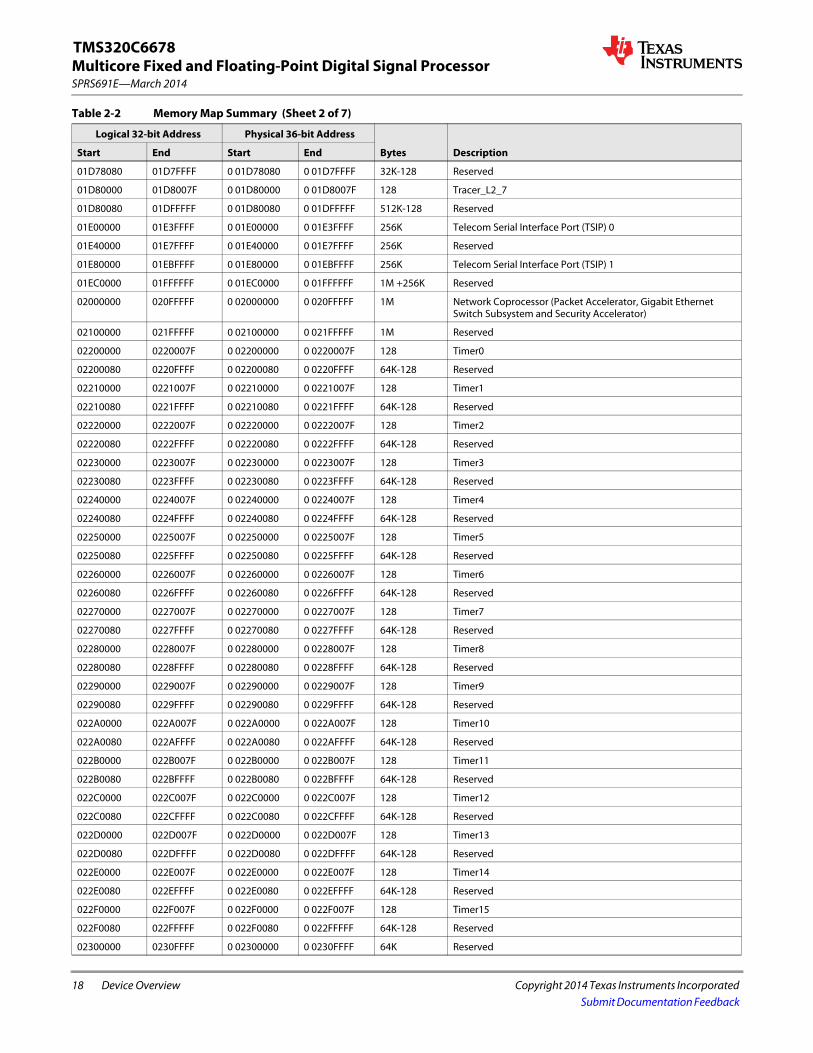
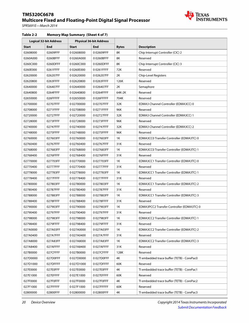
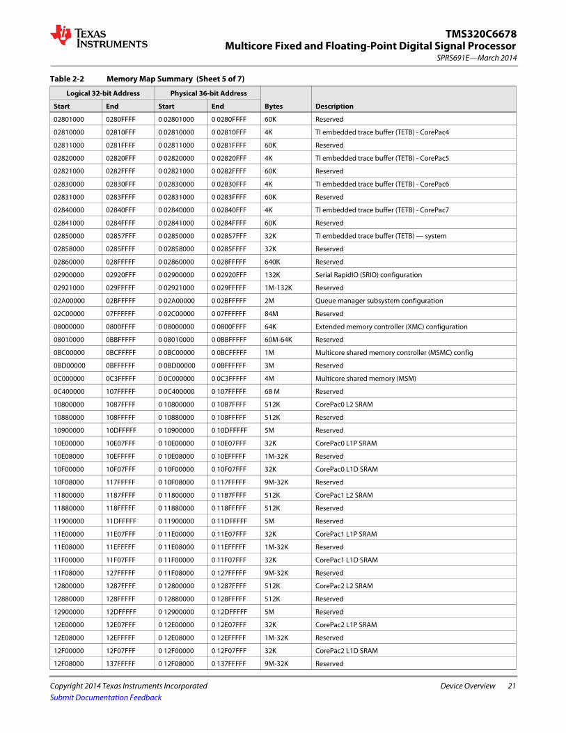
2.3 Memory Map SummaryTable 2-2 shows the memory map address ranges of the TMS320C6678 device. Table 2-2 Memory Map Summary (Sheet 1 of 7)
Logical 32-bit Address Physical 36-bit Address
Bytes DescriptionStart End Start End
00000000 007FFFFF 0 00000000 0 007FFFFF 8M Reserved
00800000 0087FFFF 0 00800000 0 0087FFFF 512K Local L2 SRAM
00880000 00DFFFFF 0 00880000 0 00DFFFFF 5M+512K Reserved
00E00000 00E07FFF 0 00E00000 0 00E07FFF 32K Local L1P SRAM
00E08000 00EFFFFF 0 00E08000 0 00EFFFFF 1M-32K Reserved
00F00000 00F07FFF 0 00F00000 0 00F07FFF 32K Local L1D SRAM
00F08000 017FFFFF 0 00F08000 0 017FFFFF 9M-32K Reserved
01800000 01BFFFFF 0 01800000 0 01BFFFFF 4M C66x CorePac Registers
01C00000 01CFFFFF 0 01C00000 0 01CFFFFF 1M Reserved
01D00000 01D0007F 0 01D00000 0 01D0007F 128 Tracer_MSMC_0
01D00080 01D07FFF 0 01D00080 0 01D07FFF 32K-128 Reserved
01D08000 01D0807F 0 01D08000 0 01D0807F 128 Tracer_MSMC_1
01D08080 01D0FFFF 0 01D08080 0 01D0FFFF 32K-128 Reserved
01D10000 01D1007F 0 01D10000 0 01D1007F 128 Tracer_MSMC_2
01D10080 01D17FFF 0 01D10080 0 01D17FFF 32K-128 Reserved
01D18000 01D1807F 0 01D18000 0 01D1807F 128 Tracer_MSMC_3
01D18080 01D1FFFF 0 01D18080 0 01D1FFFF 32K-128 Reserved
01D20000 01D2007F 0 01D20000 0 01D2007F 128 Tracer_QM_DMA
01D20080 01D27FFF 0 01D20080 0 01D27FFF 32K-128 Reserved
01D28000 01D2807F 0 01D28000 0 01D2807F 128 Tracer_DDR
01D28080 01D2FFFF 0 01D28080 0 01D2FFFF 32K-128 Reserved
01D30000 01D3007F 0 01D30000 0 01D3007F 128 Tracer_SM
01D30080 01D37FFF 0 01D30080 0 01D37FFF 32K-128 Reserved
01D38000 01D3807F 0 01D38000 0 01D3807F 128 Tracer_QM_CFG
01D38080 01D3FFFF 0 01D38080 0 01D3FFFF 32K-128 Reserved
01D40000 01D4007F 0 01D40000 0 01D4007F 128 Tracer_CFG
01D40080 01D47FFF 0 01D40080 0 01D47FFF 32K-128 Reserved
01D48000 01D4807F 0 01D48000 0 01D4807F 128 Tracer_L2_0
01D48080 01D4FFFF 0 01D48080 0 01D4FFFF 32K-128 Reserved
01D50000 01D5007F 0 01D50000 0 01D5007F 128 Tracer_L2_1
01D50080 01D57FFF 0 01D50080 0 01D57FFF 32K-128 Reserved
01D58000 01D5807F 0 01D58000 0 01D5807F 128 Tracer_L2_2
01D58080 01D5FFFF 0 01D58080 0 01D5FFFF 32K-128 Reserved
01D60000 01D6007F 0 01D60000 0 01D6007F 128 Tracer_L2_3
01D60080 01D67FFF 0 01D60080 0 01D67FFF 32K-128 Reserved
01D68000 01D6807F 0 01D68000 0 01D6807F 128 Tracer_L2_4
01D68080 01D6FFFF 0 01D68080 0 01D6FFFF 32K-128 Reserved
01D70000 01D7007F 0 01D70000 0 01D7007F 128 Tracer_L2_5
01D70080 01D77FFF 0 01D70080 0 01D77FFF 32K-128 Reserved
01D78000 01D7807F 0 01D78000 0 01D7807F 128 Tracer_L2_6
18 Device Overview Copyright 2014 Texas Instruments Incorporated
SPRS691E—March 2014Multicore Fixed and Floating-Point Digital Signal ProcessorTMS320C6678
Submit Documentation Feedback
01D78080 01D7FFFF 0 01D78080 0 01D7FFFF 32K-128 Reserved
01D80000 01D8007F 0 01D80000 0 01D8007F 128 Tracer_L2_7
01D80080 01DFFFFF 0 01D80080 0 01DFFFFF 512K-128 Reserved
01E00000 01E3FFFF 0 01E00000 0 01E3FFFF 256K Telecom Serial Interface Port (TSIP) 0
01E40000 01E7FFFF 0 01E40000 0 01E7FFFF 256K Reserved
01E80000 01EBFFFF 0 01E80000 0 01EBFFFF 256K Telecom Serial Interface Port (TSIP) 1
01EC0000 01FFFFFF 0 01EC0000 0 01FFFFFF 1M +256K Reserved
02000000 020FFFFF 0 02000000 0 020FFFFF 1M Network Coprocessor (Packet Accelerator, Gigabit Ethernet Switch Subsystem and Security Accelerator)
02100000 021FFFFF 0 02100000 0 021FFFFF 1M Reserved
02200000 0220007F 0 02200000 0 0220007F 128 Timer0
02200080 0220FFFF 0 02200080 0 0220FFFF 64K-128 Reserved
02210000 0221007F 0 02210000 0 0221007F 128 Timer1
02210080 0221FFFF 0 02210080 0 0221FFFF 64K-128 Reserved
02220000 0222007F 0 02220000 0 0222007F 128 Timer2
02220080 0222FFFF 0 02220080 0 0222FFFF 64K-128 Reserved
02230000 0223007F 0 02230000 0 0223007F 128 Timer3
02230080 0223FFFF 0 02230080 0 0223FFFF 64K-128 Reserved
02240000 0224007F 0 02240000 0 0224007F 128 Timer4
02240080 0224FFFF 0 02240080 0 0224FFFF 64K-128 Reserved
02250000 0225007F 0 02250000 0 0225007F 128 Timer5
02250080 0225FFFF 0 02250080 0 0225FFFF 64K-128 Reserved
02260000 0226007F 0 02260000 0 0226007F 128 Timer6
02260080 0226FFFF 0 02260080 0 0226FFFF 64K-128 Reserved
02270000 0227007F 0 02270000 0 0227007F 128 Timer7
02270080 0227FFFF 0 02270080 0 0227FFFF 64K-128 Reserved
02280000 0228007F 0 02280000 0 0228007F 128 Timer8
02280080 0228FFFF 0 02280080 0 0228FFFF 64K-128 Reserved
02290000 0229007F 0 02290000 0 0229007F 128 Timer9
02290080 0229FFFF 0 02290080 0 0229FFFF 64K-128 Reserved
022A0000 022A007F 0 022A0000 0 022A007F 128 Timer10
022A0080 022AFFFF 0 022A0080 0 022AFFFF 64K-128 Reserved
022B0000 022B007F 0 022B0000 0 022B007F 128 Timer11
022B0080 022BFFFF 0 022B0080 0 022BFFFF 64K-128 Reserved
022C0000 022C007F 0 022C0000 0 022C007F 128 Timer12
022C0080 022CFFFF 0 022C0080 0 022CFFFF 64K-128 Reserved
022D0000 022D007F 0 022D0000 0 022D007F 128 Timer13
022D0080 022DFFFF 0 022D0080 0 022DFFFF 64K-128 Reserved
022E0000 022E007F 0 022E0000 0 022E007F 128 Timer14
022E0080 022EFFFF 0 022E0080 0 022EFFFF 64K-128 Reserved
022F0000 022F007F 0 022F0000 0 022F007F 128 Timer15
022F0080 022FFFFF 0 022F0080 0 022FFFFF 64K-128 Reserved
02300000 0230FFFF 0 02300000 0 0230FFFF 64K Reserved
Table 2-2 Memory Map Summary (Sheet 2 of 7)
Logical 32-bit Address Physical 36-bit Address
Bytes DescriptionStart End Start End

Multicore Fixed and Floating-Point Digital Signal Processor
Copyright 2014 Texas Instruments Incorporated Device Overview 19
SPRS691E—March 2014
TMS320C6678
Submit Documentation Feedback
02310000 023101FF 0 02310000 0 023101FF 512 PLL Controller
02310200 0231FFFF 0 02310200 0 0231FFFF 64K-512 Reserved
02320000 023200FF 0 02320000 0 023200FF 256 GPIO
02320100 0232FFFF 0 02320100 0 0232FFFF 64K-256 Reserved
02330000 023303FF 0 02330000 0 023303FF 1K SmartReflex
02330400 0234FFFF 0 02330400 0 0234FFFF 127K Reserved
02350000 02350FFF 0 02350000 0 02350FFF 4K Power Sleep Controller (PSC)
02351000 0235FFFF 0 02351000 0 0235FFFF 64K-4K Reserved
02360000 023603FF 0 02360000 0 023603FF 1K Memory Protection Unit (MPU) 0
02360400 02367FFF 0 02360400 0 02367FFF 31K Reserved
02368000 023683FF 0 02368000 0 023683FF 1K Memory Protection Unit (MPU) 1
02368400 0236FFFF 0 02368400 0 0236FFFF 31K Reserved
02370000 023703FF 0 02370000 0 023703FF 1K Memory Protection Unit (MPU) 2
02370400 02377FFF 0 02370400 0 02377FFF 31K Reserved
02378000 023783FF 0 02378000 0 023783FF 1K Memory Protection Unit (MPU) 3
02378400 023FFFFF 0 02378400 0 023FFFFF 543K Reserved
02400000 0243FFFF 0 02400000 0 0243FFFF 256K Debug Subsystem Configuration
02440000 02443FFF 0 02440000 0 02443FFF 16K DSP trace formatter 0
02444000 0244FFFF 0 02444000 0 0244FFFF 48K Reserved
02450000 02453FFF 0 02450000 0 02453FFF 16K DSP trace formatter 1
02454000 0245FFFF 0 02454000 0 0245FFFF 48K Reserved
02460000 02463FFF 0 02460000 0 02463FFF 16K DSP trace formatter 2
02464000 0246FFFF 0 02464000 0 0246FFFF 48K Reserved
02470000 02473FFF 0 02470000 0 02473FFF 16K DSP trace formatter 3
02474000 0247FFFF 0 02474000 0 0247FFFF 48K Reserved
02480000 02483FFF 0 02480000 0 02483FFF 16K DSP trace formatter 4
02484000 0248FFFF 0 02484000 0 0248FFFF 48K Reserved
02490000 02493FFF 0 02490000 0 02493FFF 16K DSP trace formatter 5
02494000 0249FFFF 0 02494000 0 0249FFFF 48K Reserved
024A0000 024A3FFF 0 024A0000 0 024A3FFF 16K DSP trace formatter 6
024A4000 024AFFFF 0 024A4000 0 024AFFFF 48K Reserved
024B0000 024B3FFF 0 024B0000 0 024B3FFF 16K DSP trace formatter 7
024B4000 024BFFFF 0 024B4000 0 024BFFFF 48K Reserved
024C0000 0252FFFF 0 024C0000 0 0252FFFF 448K Reserved
02530000 0253007F 0 02530000 0 0253007F 128 I2C data & control
02530080 0253FFFF 0 02530080 0 0253FFFF 64K-128 Reserved
02540000 0254003F 0 02540000 0 0254003F 64 UART
02540400 0254FFFF 0 02540400 0 0254FFFF 64K-64 Reserved
02550000 025FFFFF 0 02550000 0 025FFFFF 704K Reserved
02600000 02601FFF 0 02600000 0 02601FFF 8K Chip Interrupt Controller (CIC) 0
02602000 02603FFF 0 02602000 0 02603FFF 8K Reserved
02604000 02605FFF 0 02604000 0 02605FFF 8K Chip Interrupt Controller (CIC) 1
02606000 02607FFF 0 02606000 0 02607FFF 8K Reserved
Table 2-2 Memory Map Summary (Sheet 3 of 7)
Logical 32-bit Address Physical 36-bit Address
Bytes DescriptionStart End Start End
20 Device Overview Copyright 2014 Texas Instruments Incorporated
SPRS691E—March 2014Multicore Fixed and Floating-Point Digital Signal ProcessorTMS320C6678
Submit Documentation Feedback
02608000 02609FFF 0 02608000 0 02609FFF 8K Chip Interrupt Controller (CIC) 2
0260A000 0260BFFF 0 0260A000 0 0260BFFF 8K Reserved
0260C000 0260DFFF 0 0260C000 0 0260DFFF 8K Chip Interrupt Controller (CIC) 3
0260E000 0261FFFF 0 0260E000 0 0261FFFF 72K Reserved
02620000 026207FF 0 02620000 0 026207FF 2K Chip-Level Registers
02620800 0263FFFF 0 02620800 0 0263FFFF 126K Reserved
02640000 026407FF 0 02640000 0 026407FF 2K Semaphore
02640800 0264FFFF 0 02640800 0 0264FFFF 64K-2K Reserved
02650000 026FFFFF 0 02650000 0 026FFFFF 704K Reserved
02700000 02707FFF 0 02700000 0 02707FFF 32K EDMA3 Channel Controller (EDMA3CC) 0
02708000 0271FFFF 0 02708000 0 0271FFFF 96K Reserved
02720000 02727FFF 0 02720000 0 02727FFF 32K EDMA3 Channel Controller (EDMA3CC) 1
02728000 0273FFFF 0 02728000 0 0273FFFF 96K Reserved
02740000 02747FFF 0 02740000 0 02747FFF 32K EDMA3 Channel Controller (EDMA3CC) 2
02748000 0275FFFF 0 02748000 0 0275FFFF 96K Reserved
02760000 027603FF 0 02760000 0 027603FF 1K EDMA3CC0 Transfer Controller (EDMA3TC) 0
02760400 02767FFF 0 02760400 0 02767FFF 31K Reserved
02768000 027683FF 0 02768000 0 027683FF 1K EDMA3CC0 Transfer Controller (EDMA3TC) 1
02768400 0276FFFF 0 02768400 0 0276FFFF 31K Reserved
02770000 027703FF 0 02770000 0 027703FF 1K EDMA3CC1 Transfer Controller (EDMA3TC) 0
02770400 02777FFF 0 02770400 0 02777FFF 31K Reserved
02778000 027783FF 0 02778000 0 027783FF 1K EDMA3CC1 Transfer Controller (EDMA3TC) 1
02778400 0277FFFF 0 02778400 0 0277FFFF 31K Reserved
02780000 027803FF 0 02780000 0 027803FF 1K EDMA3CC1 Transfer Controller (EDMA3TC) 2
02780400 02787FFF 0 02780400 0 02787FFF 31K Reserved
02788000 027883FF 0 02788000 0 027883FF 1K EDMA3CC1 Transfer Controller (EDMA3TC) 3
02788400 0278FFFF 0 02788400 0 0278FFFF 31K Reserved
02790000 027903FF 0 02790000 0 027903FF 1K EDMA3PCC2 Transfer Controller (EDMA3TC) 0
02790400 02797FFF 0 02790400 0 02797FFF 31K Reserved
02798000 027983FF 0 02798000 0 027983FF 1K EDMA3CC2 Transfer Controller (EDMA3TC) 1
02798400 0279FFFF 0 02798400 0 0279FFFF 31K Reserved
027A0000 027A03FF 0 027A0000 0 027A03FF 1K EDMA3CC2 Transfer Controller (EDMA3TC) 2
027A0400 027A7FFF 0 027A0400 0 027A7FFF 31K Reserved
027A8000 027A83FF 0 027A8000 0 027A83FF 1K EDMA3CC2 Transfer Controller (EDMA3TC) 3
027A8400 027AFFFF 0 027A8400 0 027AFFFF 31K Reserved
027B0000 027CFFFF 0 027B0000 0 027CFFFF 128K Reserved
027D0000 027D0FFF 0 027D0000 0 027D0FFF 4K TI embedded trace buffer (TETB) - CorePac0
027D1000 027DFFFF 0 027D1000 0 027DFFFF 60K Reserved
027E0000 027E0FFF 0 027E0000 0 027E0FFF 4K TI embedded trace buffer (TETB) - CorePac1
027E1000 027EFFFF 0 027E1000 0 027EFFFF 60K Reserved
027F0000 027F0FFF 0 027F0000 0 027F0FFF 4K TI embedded trace buffer (TETB) - CorePac2
027F1000 027FFFFF 0 027F1000 0 027FFFFF 60K Reserved
02800000 02800FFF 0 02800000 0 02800FFF 4K TI embedded trace buffer (TETB) - CorePac3
Table 2-2 Memory Map Summary (Sheet 4 of 7)
Logical 32-bit Address Physical 36-bit Address
Bytes DescriptionStart End Start End
Multicore Fixed and Floating-Point Digital Signal Processor
Copyright 2014 Texas Instruments Incorporated Device Overview 21
SPRS691E—March 2014
TMS320C6678
Submit Documentation Feedback
02801000 0280FFFF 0 02801000 0 0280FFFF 60K Reserved
02810000 02810FFF 0 02810000 0 02810FFF 4K TI embedded trace buffer (TETB) - CorePac4
02811000 0281FFFF 0 02811000 0 0281FFFF 60K Reserved
02820000 02820FFF 0 02820000 0 02820FFF 4K TI embedded trace buffer (TETB) - CorePac5
02821000 0282FFFF 0 02821000 0 0282FFFF 60K Reserved
02830000 02830FFF 0 02830000 0 02830FFF 4K TI embedded trace buffer (TETB) - CorePac6
02831000 0283FFFF 0 02831000 0 0283FFFF 60K Reserved
02840000 02840FFF 0 02840000 0 02840FFF 4K TI embedded trace buffer (TETB) - CorePac7
02841000 0284FFFF 0 02841000 0 0284FFFF 60K Reserved
02850000 02857FFF 0 02850000 0 02857FFF 32K TI embedded trace buffer (TETB) — system
02858000 0285FFFF 0 02858000 0 0285FFFF 32K Reserved
02860000 028FFFFF 0 02860000 0 028FFFFF 640K Reserved
02900000 02920FFF 0 02900000 0 02920FFF 132K Serial RapidIO (SRIO) configuration
02921000 029FFFFF 0 02921000 0 029FFFFF 1M-132K Reserved
02A00000 02BFFFFF 0 02A00000 0 02BFFFFF 2M Queue manager subsystem configuration
02C00000 07FFFFFF 0 02C00000 0 07FFFFFF 84M Reserved
08000000 0800FFFF 0 08000000 0 0800FFFF 64K Extended memory controller (XMC) configuration
08010000 0BBFFFFF 0 08010000 0 0BBFFFFF 60M-64K Reserved
0BC00000 0BCFFFFF 0 0BC00000 0 0BCFFFFF 1M Multicore shared memory controller (MSMC) config
0BD00000 0BFFFFFF 0 0BD00000 0 0BFFFFFF 3M Reserved
0C000000 0C3FFFFF 0 0C000000 0 0C3FFFFF 4M Multicore shared memory (MSM)
0C400000 107FFFFF 0 0C400000 0 107FFFFF 68 M Reserved
10800000 1087FFFF 0 10800000 0 1087FFFF 512K CorePac0 L2 SRAM
10880000 108FFFFF 0 10880000 0 108FFFFF 512K Reserved
10900000 10DFFFFF 0 10900000 0 10DFFFFF 5M Reserved
10E00000 10E07FFF 0 10E00000 0 10E07FFF 32K CorePac0 L1P SRAM
10E08000 10EFFFFF 0 10E08000 0 10EFFFFF 1M-32K Reserved
10F00000 10F07FFF 0 10F00000 0 10F07FFF 32K CorePac0 L1D SRAM
10F08000 117FFFFF 0 10F08000 0 117FFFFF 9M-32K Reserved
11800000 1187FFFF 0 11800000 0 1187FFFF 512K CorePac1 L2 SRAM
11880000 118FFFFF 0 11880000 0 118FFFFF 512K Reserved
11900000 11DFFFFF 0 11900000 0 11DFFFFF 5M Reserved
11E00000 11E07FFF 0 11E00000 0 11E07FFF 32K CorePac1 L1P SRAM
11E08000 11EFFFFF 0 11E08000 0 11EFFFFF 1M-32K Reserved
11F00000 11F07FFF 0 11F00000 0 11F07FFF 32K CorePac1 L1D SRAM
11F08000 127FFFFF 0 11F08000 0 127FFFFF 9M-32K Reserved
12800000 1287FFFF 0 12800000 0 1287FFFF 512K CorePac2 L2 SRAM
12880000 128FFFFF 0 12880000 0 128FFFFF 512K Reserved
12900000 12DFFFFF 0 12900000 0 12DFFFFF 5M Reserved
12E00000 12E07FFF 0 12E00000 0 12E07FFF 32K CorePac2 L1P SRAM
12E08000 12EFFFFF 0 12E08000 0 12EFFFFF 1M-32K Reserved
12F00000 12F07FFF 0 12F00000 0 12F07FFF 32K CorePac2 L1D SRAM
12F08000 137FFFFF 0 12F08000 0 137FFFFF 9M-32K Reserved
Table 2-2 Memory Map Summary (Sheet 5 of 7)
Logical 32-bit Address Physical 36-bit Address
Bytes DescriptionStart End Start End

22 Device Overview Copyright 2014 Texas Instruments Incorporated
SPRS691E—March 2014Multicore Fixed and Floating-Point Digital Signal ProcessorTMS320C6678
Submit Documentation Feedback
13800000 1387FFFF 0 13800000 0 1387FFFF 512K CorePac3 L2 SRAM
13880000 138FFFFF 0 13880000 0 138FFFFF 512K Reserved
13900000 13DFFFFF 0 13900000 0 13DFFFFF 5M Reserved
13E00000 13E07FFF 0 13E00000 0 13E07FFF 32K CorePac3 L1P SRAM
13E08000 13EFFFFF 0 13E08000 0 13EFFFFF 1M-32K Reserved
13F00000 13F07FFF 0 13F00000 0 13F07FFF 32K CorePac3 L1D SRAM
13F08000 147FFFFF 0 13F08000 0 147FFFFF 9M-32K Reserved
14800000 1487FFFF 0 14800000 0 1487FFFF 512K CorePac4 L2 SRAM
14880000 148FFFFF 0 14880000 0 148FFFFF 512K Reserved
14900000 14DFFFFF 0 14900000 0 14DFFFFF 5M Reserved
14E00000 14E07FFF 0 14E00000 0 14E07FFF 32K CorePac4 L1P SRAM
14E08000 14EFFFFF 0 14E08000 0 14EFFFFF 1M-32K Reserved
14F00000 14F07FFF 0 14F00000 0 14F07FFF 32K CorePac4 L1D SRAM
14F08000 157FFFFF 0 14F08000 0 157FFFFF 9M-32K Reserved
15800000 1587FFFF 0 15800000 0 1587FFFF 512K CorePac5 L2 SRAM
15880000 158FFFFF 0 15880000 0 158FFFFF 512K Reserved
15900000 15DFFFFF 0 15900000 0 15DFFFFF 5M Reserved
15E00000 15E07FFF 0 15E00000 0 15E07FFF 32K CorePac5 L1P SRAM
15E08000 15EFFFFF 0 15E08000 0 15EFFFFF 1M-32K Reserved
15F00000 15F07FFF 0 15F00000 0 15F07FFF 32K CorePac5 L1D SRAM
15F08000 167FFFFF 0 15F08000 0 167FFFFF 9M-32K Reserved
16800000 1687FFFF 0 16800000 0 1687FFFF 512K CorePac6 L2 SRAM
16880000 168FFFFF 0 16880000 0 168FFFFF 512K Reserved
16900000 16DFFFFF 0 16900000 0 16DFFFFF 5M Reserved
16E00000 16E07FFF 0 16E00000 0 16E07FFF 32K CorePac6 L1P SRAM
16E08000 16EFFFFF 0 16E08000 0 16EFFFFF 1M-32K Reserved
16F00000 16F07FFF 0 16F00000 0 16F07FFF 32K CorePac6 L1D SRAM
16F08000 177FFFFF 0 16F08000 0 177FFFFF 9M-32K Reserved
17800000 1787FFFF 0 17800000 0 1787FFFF 512K CorePac7 L2 SRAM
17880000 178FFFFF 0 17880000 0 178FFFFF 512K Reserved
17900000 17DFFFFF 0 17900000 0 17DFFFFF 5M Reserved
17E00000 17E07FFF 0 17E00000 0 17E07FFF 32K CorePac7 L1P SRAM
17E08000 17EFFFFF 0 17E08000 0 17EFFFFF 1M-32K Reserved
17F00000 17F07FFF 0 17F00000 0 17F07FFF 32K CorePac7 L2 SRAM
17F08000 1FFFFFFF 0 17F08000 0 1FFFFFFF 129M-32K Reserved
20000000 200FFFFF 0 20000000 0 200FFFFF 1M System trace manager (STM) configuration
20100000 20AFFFFF 0 20100000 0 20AFFFFF 10M Reserved
20B00000 20B1FFFF 0 20B00000 0 20B1FFFF 128K Boot ROM
20B20000 20BEFFFF 0 20B20000 0 20BEFFFF 832K Reserved
20BF0000 20BF01FF 0 20BF0000 0 20BF01FF 512 SPI
20BF0200 20BFFFFF 0 20BF0200 0 20BFFFFF 64K-512 Reserved
20C00000 20C000FF 0 20C00000 0 20C000FF 256 EMIF16 config
20C00100 20FFFFFF 0 20C00100 0 20FFFFFF 12M - 256 Reserved
Table 2-2 Memory Map Summary (Sheet 6 of 7)
Logical 32-bit Address Physical 36-bit Address
Bytes DescriptionStart End Start End
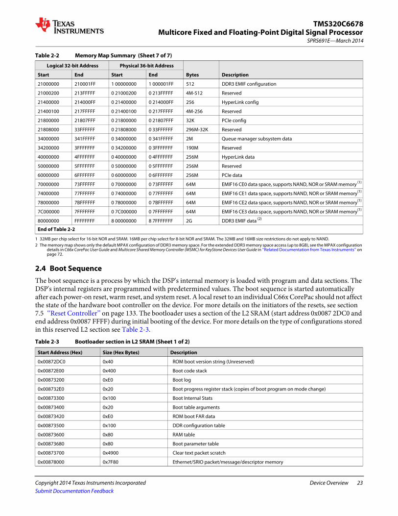
Multicore Fixed and Floating-Point Digital Signal Processor
Copyright 2014 Texas Instruments Incorporated Device Overview 23
SPRS691E—March 2014
TMS320C6678
Submit Documentation Feedback
2.4 Boot SequenceThe boot sequence is a process by which the DSP's internal memory is loaded with program and data sections. The DSP's internal registers are programmed with predetermined values. The boot sequence is started automatically after each power-on reset, warm reset, and system reset. A local reset to an individual C66x CorePac should not affect the state of the hardware boot controller on the device. For more details on the initiators of the resets, see section 7.5 ‘‘Reset Controller’’ on page 133. The bootloader uses a section of the L2 SRAM (start address 0x0087 2DC0 and end address 0x0087 FFFF) during initial booting of the device. For more details on the type of configurations stored in this reserved L2 section see Table 2-3.
21000000 210001FF 1 00000000 1 000001FF 512 DDR3 EMIF configuration
21000200 213FFFFF 0 21000200 0 213FFFFF 4M-512 Reserved
21400000 214000FF 0 21400000 0 214000FF 256 HyperLink config
21400100 217FFFFF 0 21400100 0 217FFFFF 4M-256 Reserved
21800000 21807FFF 0 21800000 0 21807FFF 32K PCIe config
21808000 33FFFFFF 0 21808000 0 33FFFFFF 296M-32K Reserved
34000000 341FFFFF 0 34000000 0 341FFFFF 2M Queue manager subsystem data
34200000 3FFFFFFF 0 34200000 0 3FFFFFFF 190M Reserved
40000000 4FFFFFFF 0 40000000 0 4FFFFFFF 256M HyperLink data
50000000 5FFFFFFF 0 50000000 0 5FFFFFFF 256M Reserved
60000000 6FFFFFFF 0 60000000 0 6FFFFFFF 256M PCIe data
70000000 73FFFFFF 0 70000000 0 73FFFFFF 64M EMIF16 CE0 data space, supports NAND, NOR or SRAM memory (1)
74000000 77FFFFFF 0 74000000 0 77FFFFFF 64M EMIF16 CE1 data space, supports NAND, NOR or SRAM memory(1)
78000000 7BFFFFFF 0 78000000 0 7BFFFFFF 64M EMIF16 CE2 data space, supports NAND, NOR or SRAM memory(1)
7C000000 7FFFFFFF 0 7C000000 0 7FFFFFFF 64M EMIF16 CE3 data space, supports NAND, NOR or SRAM memory(1)
80000000 FFFFFFFF 8 00000000 8 7FFFFFFF 2G DDR3 EMIF data (2)
End of Table 2-2
1 32MB per chip select for 16-bit NOR and SRAM. 16MB per chip select for 8-bit NOR and SRAM. The 32MB and 16MB size restrictions do not apply to NAND.2 The memory map shows only the default MPAX configuration of DDR3 memory space. For the extended DDR3 memory space access (up to 8GB), see the MPAX configuration
details in C66x CorePac User Guide and Multicore Shared Memory Controller (MSMC) for KeyStone Devices User Guide in ‘‘Related Documentation from Texas Instruments’’ on page 72.
Table 2-3 Bootloader section in L2 SRAM (Sheet 1 of 2)
Start Address (Hex) Size (Hex Bytes) Description
0x00872DC0 0x40 ROM boot version string (Unreserved)
0x00872E00 0x400 Boot code stack
0x00873200 0xE0 Boot log
0x008732E0 0x20 Boot progress register stack (copies of boot program on mode change)
0x00873300 0x100 Boot Internal Stats
0x00873400 0x20 Boot table arguments
0x00873420 0xE0 ROM boot FAR data
0x00873500 0x100 DDR configuration table
0x00873600 0x80 RAM table
0x00873680 0x80 Boot parameter table
0x00873700 0x4900 Clear text packet scratch
0x00878000 0x7F80 Ethernet/SRIO packet/message/descriptor memory
Table 2-2 Memory Map Summary (Sheet 7 of 7)
Logical 32-bit Address Physical 36-bit Address
Bytes DescriptionStart End Start End

24 Device Overview Copyright 2014 Texas Instruments Incorporated
SPRS691E—March 2014Multicore Fixed and Floating-Point Digital Signal ProcessorTMS320C6678
Submit Documentation Feedback
The C6678 supports several boot processes that begins execution at the ROM base address, which contains the bootloader code necessary to support various device boot modes. The boot processes are software-driven and use the BOOTMODE[12:0] device configuration inputs to determine the software configuration that must be completed. For more details on Boot Sequence see the DSP Bootloader for KeyStone Devices User Guide in ‘‘Related Documentation from Texas Instruments’’ on page 72.
2.5 Boot Modes Supported and PLL SettingsThe device supports several boot processes, which leverage the internal boot ROM. Most boot processes are software driven, using the BOOTMODE[3:0] device configuration inputs to determine the software configuration that must be completed. From a hardware perspective, there are two possible boot modes:
• Public ROM Boot - C66x CorePac0 is released from reset and begins executing from the L3 ROM base address. After performing the boot process (e.g., from I2C ROM, Ethernet, or RapidIO), C66x CorePac0 then begins execution from the provided boot entry point. Other C66x CorePacs are released from reset and begin executing an IDLE from the L3 ROM. They are then released from IDLE based on interrupts generated by C66x CorePac0. See the DSP Bootloader for KeyStone Devices User Guide in ‘‘Related Documentation from Texas Instruments’’ on page 72 for more details.
• Secure ROM Boot - On secure devices, the C66x CorePac0 is released from reset and begin executing from secure ROM. Software in the secure ROM will free up internal RAM pages, after which C66x CorePac0 initiates the boot process. The C66x CorePac0 performs any authentication and decryption required on the bootloaded image prior to beginning execution.
The boot process performed by the C66x CorePac0 in public ROM boot and secure ROM boot are determined by the BOOTMODE[12:0] value in the DEVSTAT register. The C66x CorePac0 reads this value, and then executes the associated boot process in software. Figure 2-2 shows the bits associated with BOOTMODE[12:0].
0x0087FF80 0x40 Small stack
0x0087FFC0 0x3C Not used
0x0087FFFC 0x4 Boot magic address
End of Table 2-3
Figure 2-2 Boot Mode Pin Decoding
Boot Mode Pins
12 11 10 9 8 7 6 5 4 3 2 1 0
PLL Mult I2C /SPI Ext Dev Cfg Device Configuration Boot Device
Table 2-3 Bootloader section in L2 SRAM (Sheet 2 of 2)
Start Address (Hex) Size (Hex Bytes) Description

Multicore Fixed and Floating-Point Digital Signal Processor
Copyright 2014 Texas Instruments Incorporated Device Overview 25
SPRS691E—March 2014
TMS320C6678
Submit Documentation Feedback
2.5.1 Boot Device Field
The Boot Device field BOOTMODE[2:0] defines the boot device that is chosen. Table 2-4 shows the supported boot modes.
Internally, these boot modes are translated by RBL into the extended boot mode value that is used in the boot parameter table. Table 2-5 shows the details of extended boot mode values.
Table 2-4 Boot Mode Pins: Boot Device Values
Bit Field Description
2-0 Boot Device Device boot mode0 = EMIF16 / No Boot1 = Serial Rapid I/O2 = Ethernet (SGMII) (PASS PLL configuration assumes input rate same as CORECLK(P|N); BOOTMODE[12:10] values drive
the PASS PLL configuration during boot)3 = Ethernet (SGMII) (PASS PLL configuration assumes input rate same as SRIOSGMIICLK(P|N); BOOTMODE[9:8] values
drive the PASS PLL configuration during boot)4 = PCIe5 = I2C6 = SPI7 = HyperLink
End of Table 2-4
Table 2-5 Extended Boot Modes
Boot Type Extended Boot Mode Value (Decimal)
Ethernet Boot Mode 10
SRIO Boot Mode 20
PCIe Boot Mode 30
I2C Master Boot Mode 40
I2C Passive Boot Mode 41
SPI Boot Mode 50
HyperLink Boot Mode 60
EMIF 16 Boot Mode 70
Sleep Boot Mode 100
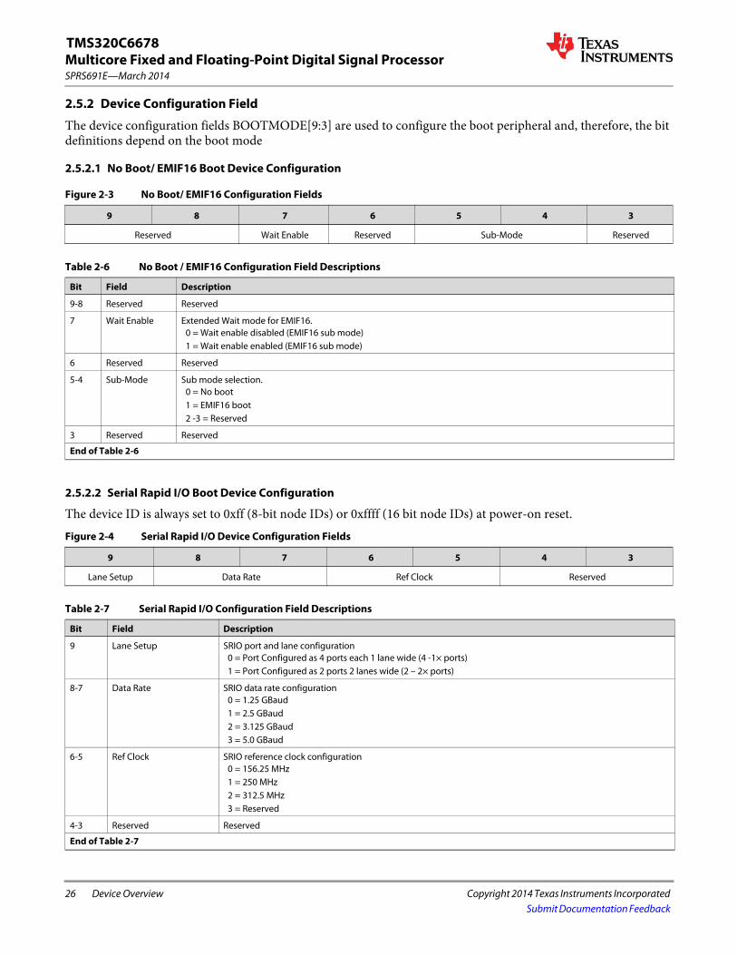
26 Device Overview Copyright 2014 Texas Instruments Incorporated
SPRS691E—March 2014Multicore Fixed and Floating-Point Digital Signal ProcessorTMS320C6678
Submit Documentation Feedback
2.5.2 Device Configuration Field
The device configuration fields BOOTMODE[9:3] are used to configure the boot peripheral and, therefore, the bit definitions depend on the boot mode
2.5.2.1 No Boot/ EMIF16 Boot Device Configuration
2.5.2.2 Serial Rapid I/O Boot Device Configuration
The device ID is always set to 0xff (8-bit node IDs) or 0xffff (16 bit node IDs) at power-on reset.
Figure 2-3 No Boot/ EMIF16 Configuration Fields
9 8 7 6 5 4 3
Reserved Wait Enable Reserved Sub-Mode Reserved
Table 2-6 No Boot / EMIF16 Configuration Field Descriptions
Bit Field Description
9-8 Reserved Reserved
7 Wait Enable Extended Wait mode for EMIF16. 0 = Wait enable disabled (EMIF16 sub mode)1 = Wait enable enabled (EMIF16 sub mode)
6 Reserved Reserved
5-4 Sub-Mode Sub mode selection.0 = No boot1 = EMIF16 boot2 -3 = Reserved
3 Reserved Reserved
End of Table 2-6
Figure 2-4 Serial Rapid I/O Device Configuration Fields
9 8 7 6 5 4 3
Lane Setup Data Rate Ref Clock Reserved
Table 2-7 Serial Rapid I/O Configuration Field Descriptions
Bit Field Description
9 Lane Setup SRIO port and lane configuration0 = Port Configured as 4 ports each 1 lane wide (4 -1× ports)1 = Port Configured as 2 ports 2 lanes wide (2 – 2× ports)
8-7 Data Rate SRIO data rate configuration0 = 1.25 GBaud1 = 2.5 GBaud2 = 3.125 GBaud3 = 5.0 GBaud
6-5 Ref Clock SRIO reference clock configuration0 = 156.25 MHz1 = 250 MHz2 = 312.5 MHz3 = Reserved
4-3 Reserved Reserved
End of Table 2-7

Multicore Fixed and Floating-Point Digital Signal Processor
Copyright 2014 Texas Instruments Incorporated Device Overview 27
SPRS691E—March 2014
TMS320C6678
Submit Documentation Feedback
In SRIO boot mode, the message mode will be enabled by default. If use of the memory reserved for received messages is required and reception of messages cannot be prevented, the master can disable the message mode by writing to the boot table and generating a boot restart.
2.5.2.3 Ethernet (SGMII) Boot Device Configuration
Note—Both of the SGMII ports have been initialized for boot. The device can boot through either of the ports. If only one SGMII port is used, then the other port will time out before the boot process completes.
2.5.2.4 PCI Boot Device Configuration
Extra device configuration is provided by the PCI bits in the DEVSTAT register.
Figure 2-5 Ethernet (SGMII) Device Configuration Fields
9 8 7 6 5 4 3
SerDes Clock Mult Ext connection Device ID
Table 2-8 Ethernet (SGMII) Configuration Field Descriptions
Bit Field Description
9-8 SerDes Clock Mult SGMII SerDes input clock. The output frequency of the PLL must be 1.25 GBs.0 = ×8 for input clock of 156.25 MHz1 = ×5 for input clock of 250 MHz2 = ×4 for input clock of 312.5 MHz3 = Reserved
7-6 Ext connection External connection mode0 = MAC to MAC connection, master with auto negotiation1 = MAC to MAC connection, slave, and MAC to PHY2 = MAC to MAC, forced link3 = MAC to fiber connection
5-3 Device ID This value can range from 0 to 7 is used in the device ID field of the Ethernet-ready frame.
End of Table 2-8
Figure 2-6 PCI Device Configuration Fields
9 8 7 6 5 4 3
Reserved BAR Config Reserved
Table 2-9 PCI Device Configuration Field Descriptions
Bit Field Description
9 Reserved Reserved
8-5 BAR Config PCIe BAR registers configuration
This value can range from 0 to 0xf. See Table 2-10.
4-3 Reserved Reserved
End of Table 2-9

28 Device Overview Copyright 2014 Texas Instruments Incorporated
SPRS691E—March 2014Multicore Fixed and Floating-Point Digital Signal ProcessorTMS320C6678
Submit Documentation Feedback
2.5.2.5 I2C Boot Device Configuration
2.5.2.5.1 I2C Master Mode
In master mode, the I2C device configuration uses ten bits of device configuration instead of seven as used in other boot modes. In this mode, the device will make the initial read of the I2C EEPROM while the PLL is in bypass mode. The initial read will contain the desired clock multiplier, which will be set up prior to any subsequent reads.
Table 2-10 BAR Config / PCIe Window Sizes
BAR cfg BAR0
32-Bit Address Translation 64-Bit Address Translation
BAR1 BAR2 BAR3 BAR4 BAR5 BAR2/3 BAR4/5
0b0000
PCIe MMRs
32 32 32 32
Clone of BAR4
0b0001 16 16 32 64
0b0010 16 32 32 64
0b0011 32 32 32 64
0b0100 16 16 64 64
0b0101 16 32 64 64
0b0110 32 32 64 64
0b0111 32 32 64 128
0b1000 64 64 128 256
0b1001 4 128 128 128
0b1010 4 128 128 256
0b1011 4 128 256 256
0b1100 256 256
0b1101 512 512
0b1110 1024 1024
0b1111 2048 2048
End of Table 2-10
Figure 2-7 I2C Master Mode Device Configuration Bit Fields
12 11 10 9 8 7 6 5 4 3
Reserved Speed Address Mode Parameter Index
Table 2-11 I2C Master Mode Device Configuration Field Descriptions (Sheet 1 of 2)
Bit Field Description
12 Reserved Reserved
11 Speed I2C data rate configuration0 = I2C slow mode. Initial data rate is CORECLK/5000 until PLLs and clocks are programmed1 = I2C fast mode. Initial data rate is CORECLK/250 until PLLs and clocks are programmed
10 Address I2C bus address configuration0 = Boot from I2C EEPROM at I2C bus address 0x501 = Boot from I2C EEPROM at I2C bus address 0x51
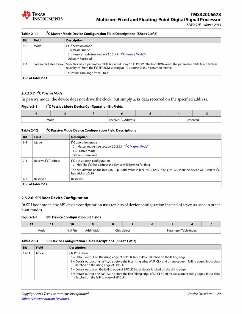
Multicore Fixed and Floating-Point Digital Signal Processor
Copyright 2014 Texas Instruments Incorporated Device Overview 29
SPRS691E—March 2014
TMS320C6678
Submit Documentation Feedback
2.5.2.5.2 I2C Passive Mode
In passive mode, the device does not drive the clock, but simply acks data received on the specified address.
2.5.2.6 SPI Boot Device Configuration
In SPI boot mode, the SPI device configuration uses ten bits of device configuration instead of seven as used in other boot modes.
9-8 Mode I2C operation mode0 = Master mode3 = Passive mode (see section 2.5.2.5.2 ‘‘I2C Passive Mode’’)Others = Reserved
7-3 Parameter Table Index Specifies which parameter table is loaded from I2C EEPROM. The boot ROM reads the parameter table (each table is 0x80 bytes) from the I2C EEPROM starting at I2C address (0x80 * parameter index).
This value can range from 0 to 31.
End of Table 2-11
Figure 2-8 I2C Passive Mode Device Configuration Bit Fields
9 8 7 6 5 4 3
Mode Receive I2C Address Reserved
Table 2-12 I2C Passive Mode Device Configuration Field Descriptions
Bit Field Description
9-8 Mode I2C operation mode0 = Master mode (see section 2.5.2.5.1 ‘‘I2C Master Mode’’)3 = Passive modeOthers = Reserved
7-5 Receive I2C Address I2C bus address configuration0 - 7h= The I2C Bus address the device will listen to for data
The actual value on the bus is 0x19 plus the value in bits [7:5]. For Ex. if bits[7:5] = 0 then the device will listen to I2C bus address 0x19.
4-3 Reserved Reserved
End of Table 2-12
Figure 2-9 SPI Device Configuration Bit Fields
12 11 10 9 8 7 6 5 4 3
Mode 4, 5 Pin Addr Width Chip Select Parameter Table Index
Table 2-13 SPI Device Configuration Field Descriptions (Sheet 1 of 2)
Bit Field Description
12-11 Mode Clk Pol / Phase0 = Data is output on the rising edge of SPICLK. Input data is latched on the falling edge.1 = Data is output one half-cycle before the first rising edge of SPICLK and on subsequent falling edges. Input data
is latched on the rising edge of SPICLK.2 = Data is output on the falling edge of SPICLK. Input data is latched on the rising edge.3 = Data is output one half-cycle before the first falling edge of SPICLK and on subsequent rising edges. Input data
is latched on the falling edge of SPICLK.
Table 2-11 I2C Master Mode Device Configuration Field Descriptions (Sheet 2 of 2)
Bit Field Description
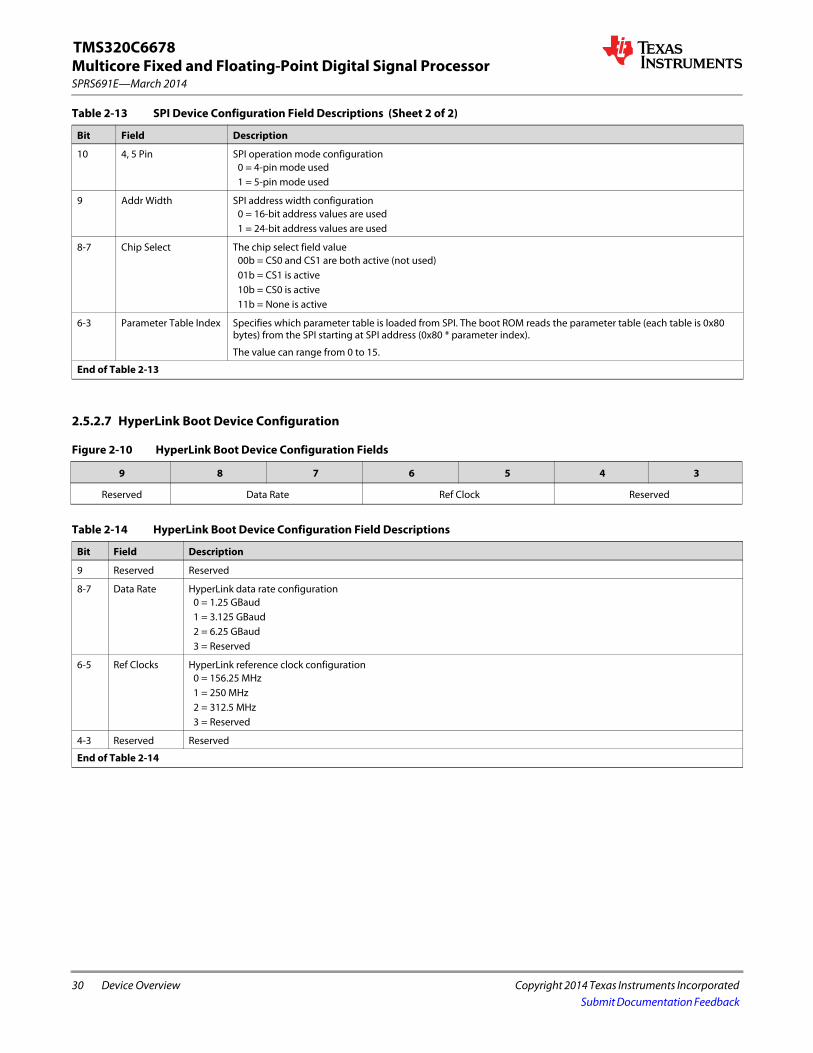
30 Device Overview Copyright 2014 Texas Instruments Incorporated
SPRS691E—March 2014Multicore Fixed and Floating-Point Digital Signal ProcessorTMS320C6678
Submit Documentation Feedback
2.5.2.7 HyperLink Boot Device Configuration
10 4, 5 Pin SPI operation mode configuration0 = 4-pin mode used1 = 5-pin mode used
9 Addr Width SPI address width configuration0 = 16-bit address values are used1 = 24-bit address values are used
8-7 Chip Select The chip select field value00b = CS0 and CS1 are both active (not used)01b = CS1 is active10b = CS0 is active11b = None is active
6-3 Parameter Table Index Specifies which parameter table is loaded from SPI. The boot ROM reads the parameter table (each table is 0x80 bytes) from the SPI starting at SPI address (0x80 * parameter index).
The value can range from 0 to 15.
End of Table 2-13
Figure 2-10 HyperLink Boot Device Configuration Fields
9 8 7 6 5 4 3
Reserved Data Rate Ref Clock Reserved
Table 2-14 HyperLink Boot Device Configuration Field Descriptions
Bit Field Description
9 Reserved Reserved
8-7 Data Rate HyperLink data rate configuration0 = 1.25 GBaud1 = 3.125 GBaud2 = 6.25 GBaud3 = Reserved
6-5 Ref Clocks HyperLink reference clock configuration0 = 156.25 MHz1 = 250 MHz2 = 312.5 MHz3 = Reserved
4-3 Reserved Reserved
End of Table 2-14
Table 2-13 SPI Device Configuration Field Descriptions (Sheet 2 of 2)
Bit Field Description

Multicore Fixed and Floating-Point Digital Signal Processor
Copyright 2014 Texas Instruments Incorporated Device Overview 31
SPRS691E—March 2014
TMS320C6678
Submit Documentation Feedback
2.5.3 Boot Parameter Table
The ROM Bootloader (RBL) uses a set of tables to carry out the boot process. The boot parameter table is the most common format the RBL employs to determine the boot flow. These boot parameter tables have certain parameters common across all the boot modes, while the rest of the parameters are unique to the boot modes. The common entries in the boot parameter table are shown in the table below:
2.5.3.1 EMIF16 Boot Parameter Table
Table 2-15 Boot Parameter Table Common Parameters
Byte Offset Name Description
0 Length The length of the table, including the length field, in bytes.
2 Checksum The 16 bits ones complement of the ones complement of the entire table. A value of 0 will disable checksum verification of the table by the boot ROM.
4 Boot Mode Internal values used by RBL for different boot modes.
6 Port Num Identifies the device port number to boot from, if applicable
8 SW PLL, MSW PLL configuration, MSW
10 SW PLL, LSW PLL configuration, LSW
End of Table 2-15
Table 2-16 EMIF16 Boot Mode Parameter Table
Byte Offset Name Description
Configured Through Boot Configuration Pins
12 Options Option for EMIF16 boot (currently none) -
14 Type Boot only from NOR flash is supported for C6678 -
16 Branch Address MSW Most significant bit for Branch address (depends on chip select) -
18 Branch Address LSW Least significant bit for Branch address (depends on chip select) -
20 Chip Select Chip Select for the NOR flash -
22 Memory Width Memory width of the Emif16 bus (16 bits) -
24 Wait Enable Extended wait mode enabled0 = Wait enable is disabled1 = Wait enable is enabled
YES
End of Table 2-16

32 Device Overview Copyright 2014 Texas Instruments Incorporated
SPRS691E—March 2014Multicore Fixed and Floating-Point Digital Signal ProcessorTMS320C6678
Submit Documentation Feedback
2.5.3.2 SRIO Boot Parameter Table
2.5.3.3 Ethernet Boot Parameter Table
Table 2-17 SRIO Boot Mode Parameter Table
Byte Offset Name Description
Configured Through Boot Configuration Pins
12 Options Bit 0 TX enable0 = SRIO transmit disable1 = SRIO transmit enable
Bit 1 Mailbox enable0 = Mailbox mode disabled. SRIO boot is in directIO mode).1 = Mailbox mode enabled. SRIO boot is in messaging mode).
Bit 2 Bypass configuration0 = Configure the SRIO1 = Bypass SRIO configuration
Bit 15-3 = Reserved
-
14 Lane Setup SRIO lane setup0 = SRIO configured as 4 1x ports1 = SRIO configured as 3 ports (2x, 1x, 1x)2 = SRIO configured as 3 ports (1x, 1x, 2x)3 = SRIO configured as 2 ports (2x, 2x)4 = SRIO configured as 1 4x portOthers = Reserved
YES
(but not all lane setup are possible through the boot configuration pins)
16 Config Index Specifies the template used for RapidIO configuration.
Must be 0 for KeyStone architecture
-
18 Node ID The node ID value to set for this device -
20 SerDes ref clk The SerDes reference clock frequency, in 1/100 MHz YES
22 Link Rate Link rate, MHz YES
24 PF Low Packet forward address range, low value -
26 PF High Packet forward address range, high value -
End of Table 2-17
Table 2-18 Ethernet Boot Mode Parameter Table (Sheet 1 of 2)
Byte Offset Name Description
Configured Through Boot Configuration Pins
12 Options Bits 2-0 Interface 101b = SGMIIOthers = Reserved
Bit 3 Half or Full duplex0 = Half Duplex1 = Full Duplex
Bit 4 Skip TX0 = Send Ethernet ready frame every 3 seconds1 = Don't send Ethernet ready frame
Bits 6-5 Initialize config00b = Switch, SerDes, SGMII and PASS are configured01b = Only SGMII and PASS are configured10b= Reserved11b = None of the Ethernet system is configured.
Bits 15-7 = Reserved
-
14 MAC High The 16 MSBs of the MAC address to receive during boot -
16 MAC Med The 16 middle bits of the MAC address to receive during boot -
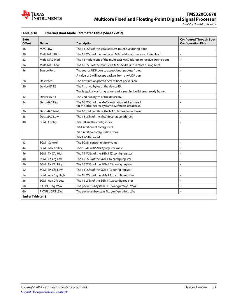
Multicore Fixed and Floating-Point Digital Signal Processor
Copyright 2014 Texas Instruments Incorporated Device Overview 33
SPRS691E—March 2014
TMS320C6678
Submit Documentation Feedback
18 MAC Low The 16 LSBs of the MAC address to receive during boot -
20 Multi MAC High The 16 MSBs of the multi-cast MAC address to receive during boot -
22 Multi MAC Med The 16 middle bits of the multi-cast MAC address to receive during boot -
24 Multi MAC Low The 16 LSBs of the multi-cast MAC address to receive during boot -
26 Source Port The source UDP port to accept boot packets from.
A value of 0 will accept packets from any UDP port
-
28 Dest Port The destination port to accept boot packets on. -
30 Device ID 12 The first two bytes of the device ID.
This is typically a string value, and is sent in the Ethernet ready frame
-
32 Device ID 34 The 2nd two bytes of the device ID. -
34 Dest MAC High The 16 MSBs of the MAC destination address usedfor the Ethernet ready frame. Default is broadcast.
-
36 Dest MAC Med The 16 middle bits of the MAC destination address -
38 Dest MAC Low The 16 LSBs of the MAC destination address -
40 SGMII Config Bits 3-0 are the config index
Bit 4 set if direct config used
Bit 5 set if no configuration done
Bits 15-6 Reserved
-
42 SGMII Control The SGMII control register value -
44 SGMII Adv Ability The SGMII ADV Ability register value -
46 SGMII TX Cfg High The 16 MSBs of the SGMII TX config register -
48 SGMII TX Cfg Low The 16 LSBs of the SGMII TX config register -
50 SGMII RX Cfg High The 16 MSBs of the SGMII RX config register -
52 SGMII RX Cfg Low The 16 LSBs of the SGMII RX config register -
54 SGMII Aux Cfg High The 16 MSBs of the SGMII Aux config register -
56 SGMII Aux Cfg Low The 16 LSBs of the SGMII Aux config register -
58 PKT PLL Cfg MSW The packet subsystem PLL configuration, MSW -
60 PKT PLL CFG LSW The packet subsystem PLL configuration, LSW -
End of Table 2-18
Table 2-18 Ethernet Boot Mode Parameter Table (Sheet 2 of 2)
Byte Offset Name Description
Configured Through Boot Configuration Pins

34 Device Overview Copyright 2014 Texas Instruments Incorporated
SPRS691E—March 2014Multicore Fixed and Floating-Point Digital Signal ProcessorTMS320C6678
Submit Documentation Feedback
2.5.3.4 PCIe Boot Parameter Table
2.5.3.5 I2C Boot Parameter Table
Table 2-19 PCIe Boot Mode Parameter Table
Byte Offset Name Description
Configured Through Boot Configuration Pins
12 Options Bit 0 Mode0 = Host mode (direct boot mode)1 = Boot table boot mode
Bit 1 Configuration of PCIe0 = PCIe is configured by RBL1 = PCIe is not configured by RBL
Bits 3-2 Reserved
Bit 4 Multiplier0 = SerDes PLL configuration is done based on SerDes register values1 = SerDes PLL configuration based on the reference clock values
Bits 15-5 Reserved
-
14 Address Width PCI address width, can be 32 or 64 -
16 Link Rate SerDes frequency, in Mbps. Can be 2500 or 5000 -
18 Reference clock Reference clock frequency, in units of 10 kHz. Value values are 10000 (100 MHz), 12500 (125 MHz), 15625 (156.25 MHz), 25000 (250 MHz), and 31250 (312.5 MHz). A value of 0 means that value is already in the SerDes configuration parameters and will not be computed by the boot ROM.
-
20 Window 1 Size Window 1 size. YES
22 Window 2 Size Window 2 size. YES
24 Window 3 Size Window 3 size. Valid only if address width is 32. YES
26 Window 4 Size Window 4 Size. Valid only if the address width is 32. YES
28 Vendor ID Vendor ID -
30 Device ID Device ID -
32 Class code Rev ID MSW Class code revision ID MSW -
34 Class code Rev ID LSW Class code revision ID LSW -
36 SerDes Cfg MSW PCIe SerDes config word, MSW -
38 SerDes Cfg LSW PCIe SerDes config word, LSW -
40 SerDes lane 0 Cfg MSW SerDes lane config word, MSW, lane 0 -
42 SerDes lane 0 Cfg LSW SerDes lane config word, LSW, lane 0 -
44 SerDes lane 1 Cfg MSW SerDes lane config word, MSW, lane 1 -
46 SerDes lane 1 Cfg LSW SerDes lane config word, LSW, lane 1 -
End of Table 2-19
Table 2-20 I2C Boot Mode Parameter Table (Sheet 1 of 2)
Byte Offset Name DescriptionConfigured Through Boot Configuration Pins
12 Option Bits 1-0 Mode00b = Boot Parameter Table Mode01b = Boot Table Mode10b = Boot Config Mode11b = Slave Receive Boot Config
Bits 15-2 Reserved
YES
14 Boot Dev Addr The I2C device address to boot from YES
16 Boot Dev Addr Ext Extended boot device address YES

Multicore Fixed and Floating-Point Digital Signal Processor
Copyright 2014 Texas Instruments Incorporated Device Overview 35
SPRS691E—March 2014
TMS320C6678
Submit Documentation Feedback
2.5.3.6 SPI Boot Parameter Table
18 Broadcast Addr I2C address used to send data in the I2C master broadcast mode. -
20 Local Address The I2C address of this device -
22 Device Freq The operating frequency of the device (MHz) -
24 Bus Frequency The desired I2C data rate (kHz) YES
26 Next Dev Addr The next device address to boot (Used only if boot config option is selected) -
28 Next Dev Addr Ext The extended next device address to boot (Used only if boot config option is selected) -
30 Address Delay The number of CPU cycles to delay between writing the address to an I2C EEPROM and reading data.
-
End of Table 2-20
Table 2-21 SPI Boot Mode Parameter Table
Byte Offset Name DescriptionConfigured Through Boot Configuration Pins
12 Options Bits 1-0 Modes00b = Load a boot parameter table from the SPI (Default mode)01b = Load boot records from the SPI (boot tables)10b = Load boot config records from the SPI (boot config tables)11b = Reserved
Bits 15-2 Reserved
-
14 Address Width The number of bytes in the SPI device address. Can be 16 or 24 bit. YES
16 NPin The operational mode, 4 or 5 pin YES
18 Chipsel The chip select used (valid in 4-pin mode only). Can be 0-3. YES
20 Mode Standard SPI mode (0-3) YES
22 C2Delay Setup time between chip assert and transaction -
24 CPU Freq MHz The speed of the CPU, in MHz -
26 Bus Freq, MHz The MHz portion of the SPI bus frequency. Default = 5 MHz -
28 Bus Freq, kHz The kHz portion of the SPI buf frequency. Default = 0 -
30 Read Addr MSW The first address to read from, MSW (valid for 24-bit address width only) YES
32 Read Addr LSW The first address to read from, LSW YES
28 Next Chip Select Next Chip Select to be used (Used only in boot config mode) -
30 Next Read Addr MSW The Next read address (used in boot config mode only) -
32 Next Read Addr LSW The Next read address (used in boot config mode only) -
End of Table 2-21
Table 2-20 I2C Boot Mode Parameter Table (Sheet 2 of 2)
Byte Offset Name DescriptionConfigured Through Boot Configuration Pins

36 Device Overview Copyright 2014 Texas Instruments Incorporated
SPRS691E—March 2014Multicore Fixed and Floating-Point Digital Signal ProcessorTMS320C6678
Submit Documentation Feedback
2.5.3.7 HyperLink Boot Parameter Table
Table 2-22 HyperLink Boot Mode Parameter Table
Byte Offset Name DescriptionConfigured Through Boot Configuration Pins
12 Options Bit 0 Mode0 = Host Mode (Direct boot mode)1 = Boot Table Boot Mode
Bit 1 Configuration of PCIe0 = HyperLink is configured by RBL1 = HyperLink is not configured by RBL
Bits 15-2 Reserved
-
14 Number of Lanes Number of lanes to be configured -
16 SerDes cfg msw HyperLink SerDes config word, MSW -
18 SerDes cfg lsw HyperLink SerDes config word, LSW -
20 SerDes CFG RX lane 0 cfg msw SerDes RX lane config word, MSW lane 0 -
22 SerDes CFG RXlane 0 cfg lsw SerDes RX lane config word, LSW, lane 0 -
24 SerDes CFG TX lane 0 cfg msw SerDes TX lane config word, MSW lane 0 -
26 SerDes CFG TXlane 0 cfg lsw SerDes TX lane config word, LSW, lane 0 -
28 SerDes CFG RX lane 1 cfg msw SerDes RX lane config word, MSW lane 1 -
30 SerDes CFG RXlane 1 cfg lsw SerDes RX lane config word, LSW, lane 1 -
32 SerDes CFG TX lane 1 cfg msw SerDes TX lane config word, MSW lane 1 -
34 SerDes CFG TXlane 1 cfg lsw SerDes TX lane config word, LSW, lane 1 -
36 SerDes CFG RX lane 2 cfg msw SerDes RX lane config word, MSW lane 2 -
38 SerDes CFG RXlane 2 cfg lsw SerDes RX lane config word, LSW, lane 2 -
40 SerDes CFG TX lane 2 cfg msw SerDes TX lane config word, MSW lane 2 -
42 SerDes CFG TXlane 2 cfg lsw SerDes TX lane config word, LSW, lane 2 -
44 SerDes CFG RX lane 3 cfg msw SerDes RX lane config word, MSW lane 3 -
46 SerDes CFG RXlane 3 cfg lsw SerDes RX lane config word, LSW, lane 3 -
48 SerDes CFG TX lane 3 cfg msw SerDes TX lane config word, MSW lane 3 -
50 SerDes CFG TXlane 3 cfg lsw SerDes TX lane config word, LSW, lane 3 -
End of Table 2-22
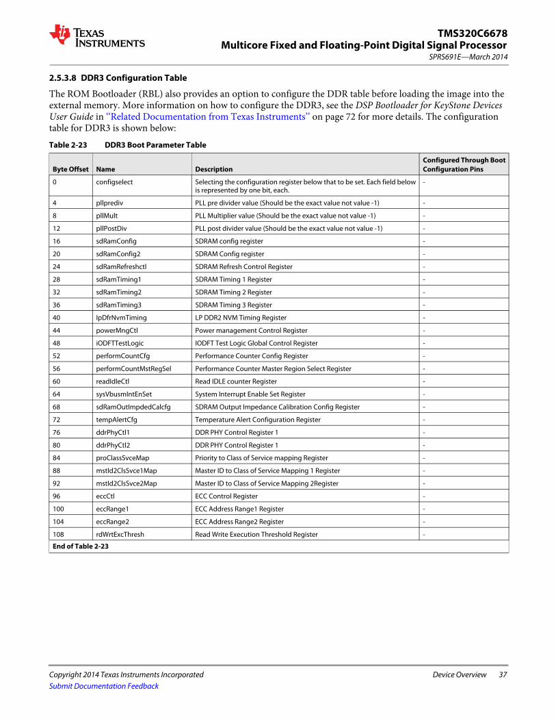
Multicore Fixed and Floating-Point Digital Signal Processor
Copyright 2014 Texas Instruments Incorporated Device Overview 37
SPRS691E—March 2014
TMS320C6678
Submit Documentation Feedback
2.5.3.8 DDR3 Configuration Table
The ROM Bootloader (RBL) also provides an option to configure the DDR table before loading the image into the external memory. More information on how to configure the DDR3, see the DSP Bootloader for KeyStone Devices User Guide in ‘‘Related Documentation from Texas Instruments’’ on page 72 for more details. The configuration table for DDR3 is shown below:Table 2-23 DDR3 Boot Parameter Table
Byte Offset Name DescriptionConfigured Through Boot Configuration Pins
0 configselect Selecting the configuration register below that to be set. Each field below is represented by one bit, each.
-
4 pllprediv PLL pre divider value (Should be the exact value not value -1) -
8 pllMult PLL Multiplier value (Should be the exact value not value -1) -
12 pllPostDiv PLL post divider value (Should be the exact value not value -1) -
16 sdRamConfig SDRAM config register -
20 sdRamConfig2 SDRAM Config register -
24 sdRamRefreshctl SDRAM Refresh Control Register -
28 sdRamTiming1 SDRAM Timing 1 Register -
32 sdRamTiming2 SDRAM Timing 2 Register -
36 sdRamTiming3 SDRAM Timing 3 Register -
40 IpDfrNvmTiming LP DDR2 NVM Timing Register -
44 powerMngCtl Power management Control Register -
48 iODFTTestLogic IODFT Test Logic Global Control Register -
52 performCountCfg Performance Counter Config Register -
56 performCountMstRegSel Performance Counter Master Region Select Register -
60 readIdleCtl Read IDLE counter Register -
64 sysVbusmIntEnSet System Interrupt Enable Set Register -
68 sdRamOutImpdedCalcfg SDRAM Output Impedance Calibration Config Register -
72 tempAlertCfg Temperature Alert Configuration Register -
76 ddrPhyCtl1 DDR PHY Control Register 1 -
80 ddrPhyCtl2 DDR PHY Control Register 1 -
84 proClassSvceMap Priority to Class of Service mapping Register -
88 mstId2ClsSvce1Map Master ID to Class of Service Mapping 1 Register -
92 mstId2ClsSvce2Map Master ID to Class of Service Mapping 2Register -
96 eccCtl ECC Control Register -
100 eccRange1 ECC Address Range1 Register -
104 eccRange2 ECC Address Range2 Register -
108 rdWrtExcThresh Read Write Execution Threshold Register -
End of Table 2-23

38 Device Overview Copyright 2014 Texas Instruments Incorporated
SPRS691E—March 2014Multicore Fixed and Floating-Point Digital Signal ProcessorTMS320C6678
Submit Documentation Feedback
2.5.4 PLL Boot Configuration Settings
The PLL default settings are determined by the BOOTMODE[12:10] bits. The table below shows settings for various input clock frequencies.
OUTPUT_DIVIDE is the value of the field of SECCTL[22:19]. This will set the PLL to the maximum clock setting for the device (with OUTPUT_DIVIDE=1, by default).
CLK = CLKIN × ((PLLM+1) ÷ ((OUTPUT_DIVIDE+1) × (PLLD+1)))The configuration for the PASS PLL is also shown. The PASS PLL is configured with these values only if the Ethernet boot mode is selected with the input clock set to match the main PLL clock (not the PASS clock). See Table 2-4 for details on configuring Ethernet boot mode. The output from the PASS PLL goes through an on-chip divider to reduce the operating frequency before reaching the NETCP. The PASS PLL generates 1050 MHz, and after the chip divider (=3), feeds 350 MHz to the NETCP.
The Main PLL is controlled using a PLL controller and a chip-level MMR. The DDR3 PLL and PASS PLL are controlled by chip level MMRs. For details on how to set up the PLL see section 7.6 ‘‘Main PLL and PLL Controller’’ on page 140. For details on the operation of the PLL controller module, see the Phase Locked Loop (PLL) for KeyStone Devices User Guide in ‘‘Related Documentation from Texas Instruments’’ on page 72.
2.6 Second-Level BootloadersAny of the boot modes can be used to download a second-level bootloader. A second-level bootloader allows for any level of customization to current boot methods as well as the definition of a completely customized boot.
Table 2-24 C66x DSP System PLL Configuration (1)
1 The PLL boot configuration of initial silicon 1.0 may support only 800 MHz, 1000 MHz, and 1200 MHz frequencies by default.
BOOTMODE[12:10]
Input ClockFreq (MHz)
800 MHz Device 1000 MHz Device 1200 MHz Device 1250 MHz Device PASS PLL = 350 MHz (2)
2 The PASS PLL generates 1050 MHz and is internally divided by 3 to supply 350 MHz to the packet accelerator.
PLLD
PLLM
DSP
Fre
q(M
Hz)
PLLD
PLLM
DSP
Fre
q(M
Hz)
PLLD
PLLM
DSP
Fre
q(M
Hz)
PLLD
PLLM
DSP
Fre
q(M
Hz)
PLLD
PLLM
DSP
Fre
q(M
Hz)
0b000 50.00 0 31 800 0 39 1000 0 47 1200 0 49 1250 0 41 1050
0b001 66.67 0 23 800.04 0 29 1000.05 0 35 1200.06 1 74 1250.06 1 62 1050.053
0b010 80.00 0 19 800 0 24 1000 0 29 1200 3 124 1250 3 104 1050
0b011 100.00 0 15 800 0 19 1000 0 23 1200 0 24 1250 0 20 1050
0b100 156.25 24 255 800 4 63 1000 24 383 1200 0 15 1250 24 335 1050
0b101 250.00 4 31 800 0 7 1000 4 47 1200 0 9 1250 4 41 1050
0b110 312.50 24 127 800 4 31 1000 24 191 1200 0 7 1250 24 167 1050
0b111 122.88 47 624 800 28 471 999.989 31 624 1200 2 60 1249.28 11 204 1049.6
End of Table 2-24
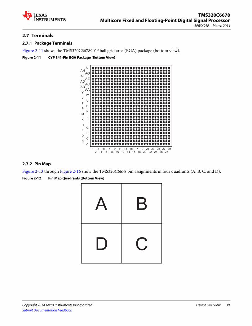
Multicore Fixed and Floating-Point Digital Signal Processor
Copyright 2014 Texas Instruments Incorporated Device Overview 39
SPRS691E—March 2014
TMS320C6678
Submit Documentation Feedback
2.7 Terminals2.7.1 Package Terminals
Figure 2-11 shows the TMS320C6678CYP ball grid area (BGA) package (bottom view).Figure 2-11 CYP 841-Pin BGA Package (Bottom View)
2.7.2 Pin Map
Figure 2-13 through Figure 2-16 show the TMS320C6678 pin assignments in four quadrants (A, B, C, and D).Figure 2-12 Pin Map Quadrants (Bottom View)
AD
B
D
F
H
K
M
P
T
V
Y
AB
AF
AH
A
C
E
G
J
L
N
R
U
W
AA
AC
AE
AG
AJ
2 4 6 8 10 12 14 16 18 20 22 24 26 281 3 5 7 9 11 13 15 17 19 21 23 25 27 29
A B
CD
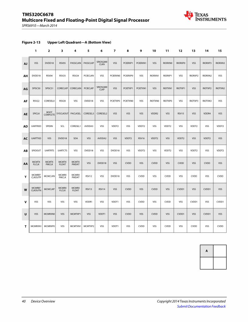
40 Device Overview Copyright 2014 Texas Instruments Incorporated
SPRS691E—March 2014Multicore Fixed and Floating-Point Digital Signal ProcessorTMS320C6678
Submit Documentation Feedback
Figure 2-13 Upper Left Quadrant—A (Bottom View)
1 2 3 4 5 6 7 8 9 10 11 12 13 14 15
AJ VSS DVDD18 RSV05 PASSCLKN PASSCLKP SRIOSGMIICLKN VSS PCIERXP1 PCIERXN1 VSS RIORXN0 RIORXP0 VSS RIORXP3 RIORXN3
AH DVDD18 RSV04 RSV25 RSV24 PCIECLKN VSS PCIERXN0 PCIERXP0 VSS RIORXN1 RIORXP1 VSS RIORXP2 RIORXN2 VSS
AG SPISCS0 SPISCS1 CORECLKP CORECLKN PCIECLKP SRIOSGMIICLKP VSS PCIETXP1 PCIETXN1 VSS RIOTXN1 RIOTXP1 VSS RIOTXP2 RIOTXN2
AF RSV22 CORESEL0 RSV20 VSS DVDD18 VSS PCIETXP0 PCIETXN0 VSS RIOTXN0 RIOTXP0 VSS RIOTXP3 RIOTXN3 VSS
AE SPICLK BOOTCOMPLETE SYSCLKOUT PACLKSEL CORESEL3 CORESEL2 VSS VSS VSS VDDR2 VSS RSV15 VSS VDDR4 VSS
AD UARTRXD SPIDIN SCL CORESEL1 AVDDA3 VSS VDDT2 VSS VDDT2 VSS VDDT2 VSS VDDT2 VSS VDDT2
AC UARTTXD VSS DVDD18 SDA VSS AVDDA2 VSS VDDT2 RSV16 VDDT2 VSS VDDT2 VSS VDDT2 VSS
AB SPIDOUT UARTRTS UARTCTS VSS DVDD18 VSS DVDD18 VSS VDDT2 VSS VDDT2 VSS VDDT2 VSS VDDT2
AAMCMTXFLCLK
MCMTXPMCLK
MCMTXFLDAT
MCMTXPMDAT VSS DVDD18 VSS CVDD VSS CVDD VSS CVDD VSS CVDD VSS
YMCMREFCLKOUTP MCMCLKN MCMRX
PMCLKMCMRXPMDAT RSV12 VSS DVDD18 VSS CVDD VSS CVDD VSS CVDD VSS CVDD
WMCMREFCLKOUTN MCMCLKP MCMRX
FLCLKMCMRXFLDAT RSV13 RSV14 VSS CVDD VSS CVDD VSS CVDD1 VSS CVDD1 VSS
V VSS VSS VSS VSS VDDR1 VSS VDDT1 VSS CVDD VSS CVDD VSS CVDD1 VSS CVDD1
U VSS MCMRXN0 VSS MCMTXP1 VSS VDDT1 VSS CVDD VSS CVDD VSS CVDD1 VSS CVDD1 VSS
T MCMRXN1 MCMRXP0 VSS MCMTXN1 MCMTXP2 VSS VDDT1 VSS CVDD VSS CVDD VSS CVDD VSS CVDD
A
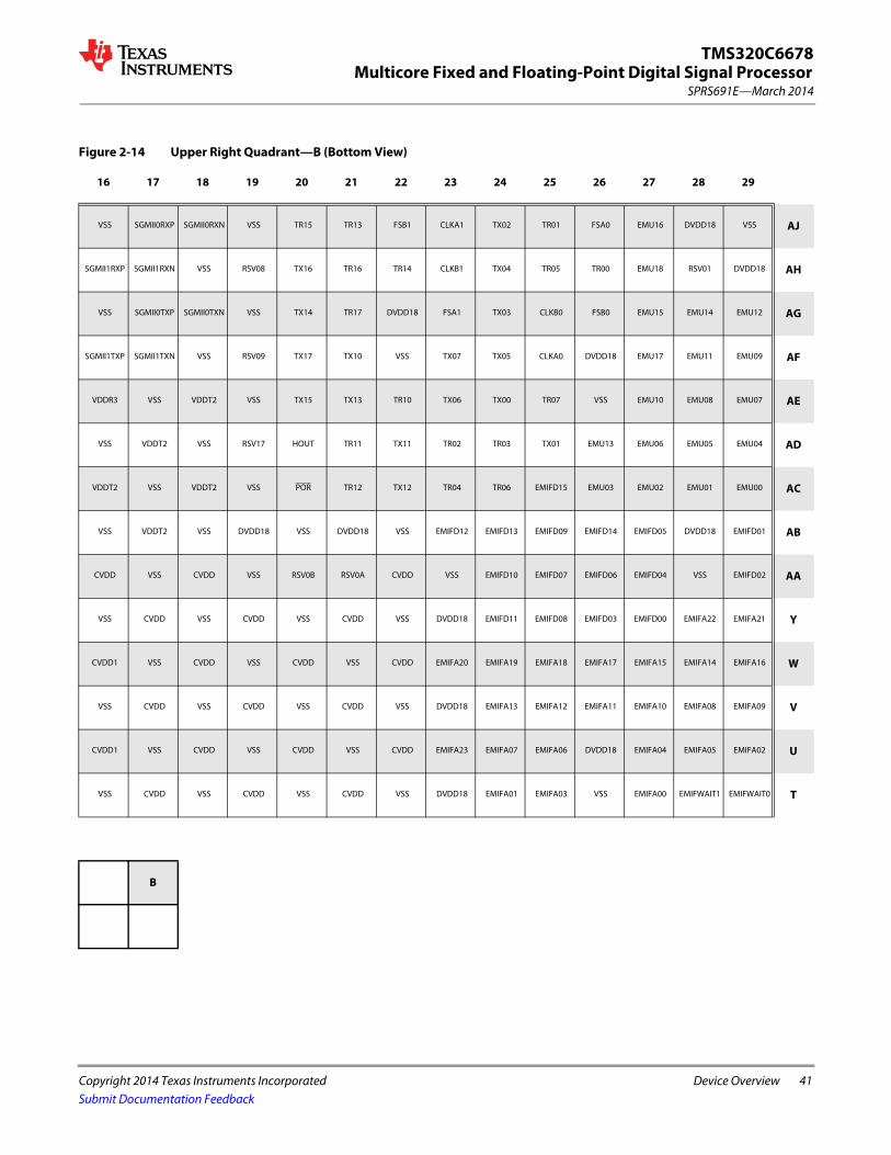
Multicore Fixed and Floating-Point Digital Signal Processor
Copyright 2014 Texas Instruments Incorporated Device Overview 41
SPRS691E—March 2014
TMS320C6678
Submit Documentation Feedback
Figure 2-14 Upper Right Quadrant—B (Bottom View)
16 17 18 19 20 21 22 23 24 25 26 27 28 29
VSS SGMII0RXP SGMII0RXN VSS TR15 TR13 FSB1 CLKA1 TX02 TR01 FSA0 EMU16 DVDD18 VSS AJ
SGMII1RXP SGMII1RXN VSS RSV08 TX16 TR16 TR14 CLKB1 TX04 TR05 TR00 EMU18 RSV01 DVDD18 AH
VSS SGMII0TXP SGMII0TXN VSS TX14 TR17 DVDD18 FSA1 TX03 CLKB0 FSB0 EMU15 EMU14 EMU12 AG
SGMII1TXP SGMII1TXN VSS RSV09 TX17 TX10 VSS TX07 TX05 CLKA0 DVDD18 EMU17 EMU11 EMU09 AF
VDDR3 VSS VDDT2 VSS TX15 TX13 TR10 TX06 TX00 TR07 VSS EMU10 EMU08 EMU07 AE
VSS VDDT2 VSS RSV17 HOUT TR11 TX11 TR02 TR03 TX01 EMU13 EMU06 EMU05 EMU04 AD
VDDT2 VSS VDDT2 VSS POR TR12 TX12 TR04 TR06 EMIFD15 EMU03 EMU02 EMU01 EMU00 AC
VSS VDDT2 VSS DVDD18 VSS DVDD18 VSS EMIFD12 EMIFD13 EMIFD09 EMIFD14 EMIFD05 DVDD18 EMIFD01 AB
CVDD VSS CVDD VSS RSV0B RSV0A CVDD VSS EMIFD10 EMIFD07 EMIFD06 EMIFD04 VSS EMIFD02 AA
VSS CVDD VSS CVDD VSS CVDD VSS DVDD18 EMIFD11 EMIFD08 EMIFD03 EMIFD00 EMIFA22 EMIFA21 Y
CVDD1 VSS CVDD VSS CVDD VSS CVDD EMIFA20 EMIFA19 EMIFA18 EMIFA17 EMIFA15 EMIFA14 EMIFA16 W
VSS CVDD VSS CVDD VSS CVDD VSS DVDD18 EMIFA13 EMIFA12 EMIFA11 EMIFA10 EMIFA08 EMIFA09 V
CVDD1 VSS CVDD VSS CVDD VSS CVDD EMIFA23 EMIFA07 EMIFA06 DVDD18 EMIFA04 EMIFA05 EMIFA02 U
VSS CVDD VSS CVDD VSS CVDD VSS DVDD18 EMIFA01 EMIFA03 VSS EMIFA00 EMIFWAIT1 EMIFWAIT0 T
B
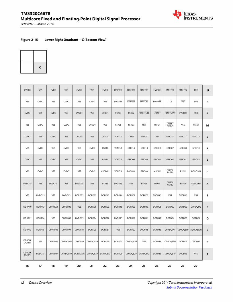
42 Device Overview Copyright 2014 Texas Instruments Incorporated
SPRS691E—March 2014Multicore Fixed and Floating-Point Digital Signal ProcessorTMS320C6678
Submit Documentation Feedback
Figure 2-15 Lower Right Quadrant—C (Bottom View)
C
CVDD1 VSS CVDD VSS CVDD VSS CVDD EMIFBE1 EMIFBE0 EMIFCE3 EMIFOE EMIFCE1 EMIFCE2 TDO R
VSS CVDD VSS CVDD VSS CVDD VSS DVDD18 EMIFWE EMIFCE0 EMIFRW TDI TRST TMS P
CVDD VSS CVDD VSS CVDD1 VSS CVDD1 RSV03 RSV02 RESETFULL LRESET RESETSTAT DVDD18 TCK N
VSS CVDD VSS CVDD VSS CVDD1 VSS RSV26 RSV27 NMI TIMO1 LRESETNMIEN VSS RESET M
CVDD VSS CVDD VSS CVDD1 VSS CVDD1 VCNTL0 TIMI0 TIMO0 TIMI1 GPIO15 GPIO11 GPIO12 L
VSS CVDD VSS CVDD VSS CVDD RSV10 VCNTL1 GPIO14 GPIO13 GPIO09 GPIO07 GPIO08 GPIO10 K
CVDD VSS CVDD VSS CVDD VSS RSV11 VCNTL2 GPIO06 GPIO04 GPIO03 GPIO05 GPIO01 GPIO02 J
VSS CVDD VSS CVDD VSS CVDD AVDDA1 VCNTL3 DVDD18 GPIO00 MDCLK DDRSLRATE1 RSV06 DDRCLKN H
DVDD15 VSS DVDD15 VSS DVDD15 VSS PTV15 DVDD15 VSS RSV21 MDIO DDRSLRATE0 RSV07 DDRCLKP G
VSS DVDD15 VSS DVDD15 DDRD25 DDRD27 DDRD17 DDRD16 DDRD08 DDRD07 DVDD15 VSS DVDD15 VSS F
DDRA10 DDRA12 DDRCKE1 DDRCB00 VSS DDRD26 DDRD23 DDRD19 DDRD09 DDRD10 DDRD06 DDRD02 DDRD00 DDRDQM0 E
DDRA11 DDRA14 VSS DDRCB02 DVDD15 DDRD24 DDRD28 DVDD15 DDRD18 DDRD11 DDRD12 DDRD04 DDRD03 DDRD01 D
DDRA13 DDRA15 DDRCB05 DDRCB04 DDRCB01 DDRD29 DDRD31 VSS DDRD22 DVDD15 DDRD13 DDRDQM1 DDRDQS0P DDRDQS0N C
DDRCLKOUTN1 VSS DDRCB06 DDRDQS8N DDRCB03 DDRDQS3N DDRD30 DDRD21 DDRDQS2N VSS DDRD14 DDRDQS1N DDRD05 DVDD15 B
DDRCLKOUTP1 DVDD15 DDRCB07 DDRDQS8P DDRDQM8 DDRDQS3P DDRDQM3 DDRD20 DDRDQS2P DDRDQM2 DDRD15 DDRDQS1P DVDD15 VSS A
16 17 18 19 20 21 22 23 24 25 26 27 28 29
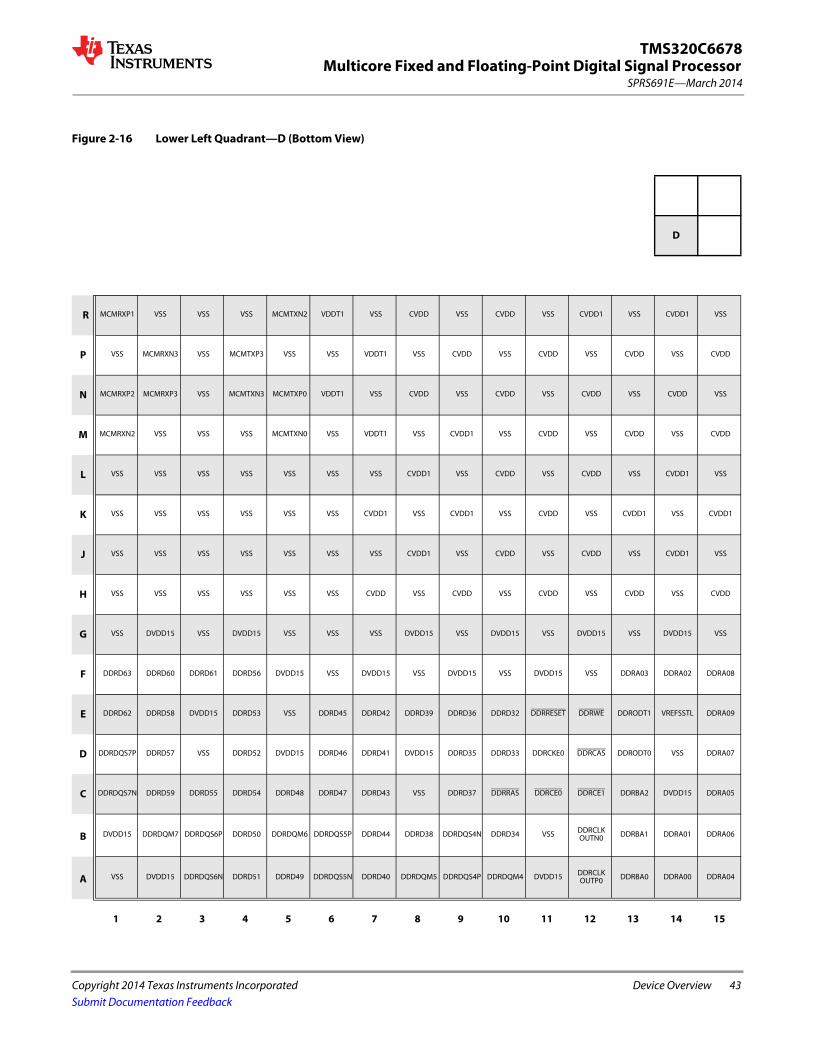
Multicore Fixed and Floating-Point Digital Signal Processor
Copyright 2014 Texas Instruments Incorporated Device Overview 43
SPRS691E—March 2014
TMS320C6678
Submit Documentation Feedback
Figure 2-16 Lower Left Quadrant—D (Bottom View)
D
R MCMRXP1 VSS VSS VSS MCMTXN2 VDDT1 VSS CVDD VSS CVDD VSS CVDD1 VSS CVDD1 VSS
P VSS MCMRXN3 VSS MCMTXP3 VSS VSS VDDT1 VSS CVDD VSS CVDD VSS CVDD VSS CVDD
N MCMRXP2 MCMRXP3 VSS MCMTXN3 MCMTXP0 VDDT1 VSS CVDD VSS CVDD VSS CVDD VSS CVDD VSS
M MCMRXN2 VSS VSS VSS MCMTXN0 VSS VDDT1 VSS CVDD1 VSS CVDD VSS CVDD VSS CVDD
L VSS VSS VSS VSS VSS VSS VSS CVDD1 VSS CVDD VSS CVDD VSS CVDD1 VSS
K VSS VSS VSS VSS VSS VSS CVDD1 VSS CVDD1 VSS CVDD VSS CVDD1 VSS CVDD1
J VSS VSS VSS VSS VSS VSS VSS CVDD1 VSS CVDD VSS CVDD VSS CVDD1 VSS
H VSS VSS VSS VSS VSS VSS CVDD VSS CVDD VSS CVDD VSS CVDD VSS CVDD
G VSS DVDD15 VSS DVDD15 VSS VSS VSS DVDD15 VSS DVDD15 VSS DVDD15 VSS DVDD15 VSS
F DDRD63 DDRD60 DDRD61 DDRD56 DVDD15 VSS DVDD15 VSS DVDD15 VSS DVDD15 VSS DDRA03 DDRA02 DDRA08
E DDRD62 DDRD58 DVDD15 DDRD53 VSS DDRD45 DDRD42 DDRD39 DDRD36 DDRD32 DDRRESET DDRWE DDRODT1 VREFSSTL DDRA09
D DDRDQS7P DDRD57 VSS DDRD52 DVDD15 DDRD46 DDRD41 DVDD15 DDRD35 DDRD33 DDRCKE0 DDRCAS DDRODT0 VSS DDRA07
C DDRDQS7N DDRD59 DDRD55 DDRD54 DDRD48 DDRD47 DDRD43 VSS DDRD37 DDRRAS DDRCE0 DDRCE1 DDRBA2 DVDD15 DDRA05
B DVDD15 DDRDQM7 DDRDQS6P DDRD50 DDRDQM6 DDRDQS5P DDRD44 DDRD38 DDRDQS4N DDRD34 VSS DDRCLKOUTN0 DDRBA1 DDRA01 DDRA06
A VSS DVDD15 DDRDQS6N DDRD51 DDRD49 DDRDQS5N DDRD40 DDRDQM5 DDRDQS4P DDRDQM4 DVDD15 DDRCLKOUTP0 DDRBA0 DDRA00 DDRA04
1 2 3 4 5 6 7 8 9 10 11 12 13 14 15

44 Device Overview Copyright 2014 Texas Instruments Incorporated
SPRS691E—March 2014Multicore Fixed and Floating-Point Digital Signal ProcessorTMS320C6678
Submit Documentation Feedback
2.8 Terminal FunctionsThe terminal functions table (Table 2-26) identifies the external signal names, the associated pin (ball) numbers, the pin type (I, O/Z, or I/O/Z), whether the pin has any internal pullup/pulldown resistors, and gives functional pin descriptions. This table is arranged by function. The power terminal functions table (Table 2-27) lists the various power supply pins and ground pins and gives functional pin descriptions. Table 2-28 shows all pins arranged by signal name. Table 2-29 shows all pins arranged by ball number.
There are 17 pins that have a secondary function as well as a primary function. The secondary function is indicated with a dagger (†).
For more detailed information on device configuration, peripheral selection, multiplexed/shared pins, and pullup/pulldown resistors, see section 3.4 ‘‘Pullup/Pulldown Resistors’’ on page 97.
Use the symbol definitions in Table 2-25 when reading Table 2-26.Table 2-25 I/O Functional Symbol Definitions
Functional Symbol Definition
Table 2-26Column Heading
IPD or IPU
Internal 100-μA pulldown or pullup is provided for this terminal. In most systems, a 1-k resistor can be used to oppose the IPD/IPU. For more detailed information on pulldown/pullup resistors and situations in which external pulldown/pullup resistors are required, see the Hardware Design Guide for KeyStone I Devices in ‘‘Related Documentation from Texas Instruments’’ on page 72.
IPD/IPU
A Analog signal Type
GND Ground Type
I Input terminal Type
O Output terminal Type
S Supply voltage Type
Z Three-state terminal or high impedance Type
End of Table 2-25
Table 2-26 Terminal Functions — Signals and Control by Function (Sheet 1 of 13)
Signal Name Ball No. Type IPD/IPU Description
Boot Configuration Pins
LENDIAN † H25 IOZ UP Endian configuration pin (Pin shared with GPIO[0])
BOOTMODE00 † J28 IOZ Down
See Section 2.5 ‘‘Boot Modes Supported and PLL Settings’’ on page 24 for more details
(Pins shared with GPIO[1:13])
BOOTMODE01† J29 IOZ Down
BOOTMODE02 † J26 IOZ Down
BOOTMODE03 † J25 IOZ Down
BOOTMODE04 † J27 IOZ Down
BOOTMODE05 † J24 IOZ Down
BOOTMODE06 † K27 IOZ Down
BOOTMODE07 † K28 IOZ Down
BOOTMODE08 † K26 IOZ Down
BOOTMODE09 † K29 IOZ Down
BOOTMODE10 † L28 IOZ Down
BOOTMODE11 † L29 IOZ Down
BOOTMODE12 † K25 IOZ Down

Multicore Fixed and Floating-Point Digital Signal Processor
Copyright 2014 Texas Instruments Incorporated Device Overview 45
SPRS691E—March 2014
TMS320C6678
Submit Documentation Feedback
PCIESSMODE0 † K24 IOZ DownPCIe Mode selection pins (Pins shared with GPIO[14:15])
PCIESSMODE1 † L27 IOZ Down
PCIESSEN † L24 I Down PCIe module enable (Pin shared with TIMI0)
Clock / Reset
CORECLKP AG3 ICore Clock Input to main PLL.
CORECLKN AG4 I
SRIOSGMIICLKP AG6 IRapidIO/SGMII Reference Clock to drive the RapidIO and SGMII SerDes
SRIOSGMIICLKN AJ6 I
DDRCLKP G29 IDDR Reference Clock Input to DDR PLL (
DDRCLKN H29 I
PCIECLKP AG5 IPCIe Clock Input to drive PCIe SerDes
PCIECLKN AH5 I
MCMCLKP W2 IHyperLink Reference Clock to drive the HyperLink SerDes
MCMCLKN Y2 I
PASSCLKP AJ5 INetwork Coprocessor (PASS PLL) Reference Clock
PASSCLKN AJ4 I
AVDDA1 H22 P SYS_CLK PLL Power Supply Pin
AVDDA2 AC6 P DDR_CLK PLL Power Supply Pin
AVDDA3 AD5 P PASS_CLK PLL Power Supply Pin
SYSCLKOUT AE3 OZ Down System Clock Output to be used as a general purpose output clock for debug purposes
PACLKSEL AE4 I Down PA clock select to choose between core clock and PASSCLK pins
HOUT AD20 OZ UP Interrupt output pulse created by IPCGRH
NMI M25 I UP Non-maskable Interrupt
LRESET N26 I UP Warm Reset
LRESETNMIEN M27 I UP Enable for core selects
CORESEL0 AF2 I Down
Select for the target core for LRESET and NMI. For more details see Table 7-47‘‘NMI and Local Reset Timing Requirements’’ on page 190
CORESEL1 AD4 I Down
CORESEL2 AE6 I Down
CORESEL3 AE5 I Down
RESETFULL N25 I UP Full Reset
RESET M29 I UP Warm Reset of non isolated portion on the IC
POR AC20 I Power-on Reset
RESETSTAT N27 O UP Reset Status Output
BOOTCOMPLETE AE2 OZ Down Boot progress indication output
PTV15 G22 A PTV Compensation NMOS Reference Input. A precision resistor placed between the PTV15 pin and ground is used to closely tune the output impedance of the DDR interface drivers to 50 . Presently the recommended value for this 1% resistor is 45.3 .
Table 2-26 Terminal Functions — Signals and Control by Function (Sheet 2 of 13)
Signal Name Ball No. Type IPD/IPU Description
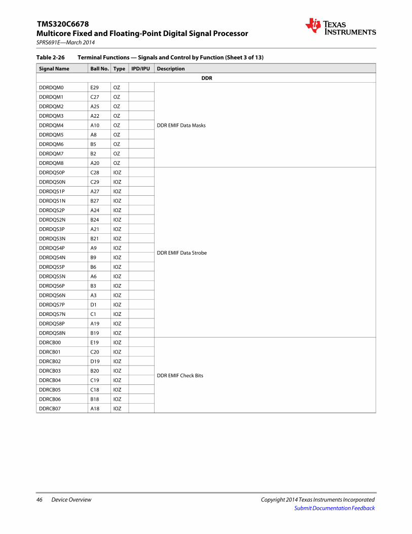
46 Device Overview Copyright 2014 Texas Instruments Incorporated
SPRS691E—March 2014Multicore Fixed and Floating-Point Digital Signal ProcessorTMS320C6678
Submit Documentation Feedback
DDR
DDRDQM0 E29 OZ
DDR EMIF Data Masks
DDRDQM1 C27 OZ
DDRDQM2 A25 OZ
DDRDQM3 A22 OZ
DDRDQM4 A10 OZ
DDRDQM5 A8 OZ
DDRDQM6 B5 OZ
DDRDQM7 B2 OZ
DDRDQM8 A20 OZ
DDRDQS0P C28 IOZ
DDR EMIF Data Strobe
DDRDQS0N C29 IOZ
DDRDQS1P A27 IOZ
DDRDQS1N B27 IOZ
DDRDQS2P A24 IOZ
DDRDQS2N B24 IOZ
DDRDQS3P A21 IOZ
DDRDQS3N B21 IOZ
DDRDQS4P A9 IOZ
DDRDQS4N B9 IOZ
DDRDQS5P B6 IOZ
DDRDQS5N A6 IOZ
DDRDQS6P B3 IOZ
DDRDQS6N A3 IOZ
DDRDQS7P D1 IOZ
DDRDQS7N C1 IOZ
DDRDQS8P A19 IOZ
DDRDQS8N B19 IOZ
DDRCB00 E19 IOZ
DDR EMIF Check Bits
DDRCB01 C20 IOZ
DDRCB02 D19 IOZ
DDRCB03 B20 IOZ
DDRCB04 C19 IOZ
DDRCB05 C18 IOZ
DDRCB06 B18 IOZ
DDRCB07 A18 IOZ
Table 2-26 Terminal Functions — Signals and Control by Function (Sheet 3 of 13)
Signal Name Ball No. Type IPD/IPU Description
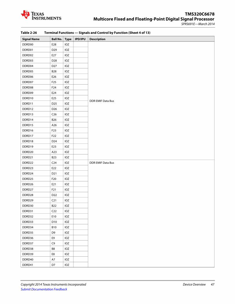
Multicore Fixed and Floating-Point Digital Signal Processor
Copyright 2014 Texas Instruments Incorporated Device Overview 47
SPRS691E—March 2014
TMS320C6678
Submit Documentation Feedback
DDRD00 E28 IOZ
DDR EMIF Data Bus
DDRD01 D29 IOZ
DDRD02 E27 IOZ
DDRD03 D28 IOZ
DDRD04 D27 IOZ
DDRD05 B28 IOZ
DDRD06 E26 IOZ
DDRD07 F25 IOZ
DDRD08 F24 IOZ
DDRD09 E24 IOZ
DDRD10 E25 IOZ
DDRD11 D25 IOZ
DDRD12 D26 IOZ
DDRD13 C26 IOZ
DDRD14 B26 IOZ
DDRD15 A26 IOZ
DDRD16 F23 IOZ
DDRD17 F22 IOZ
DDRD18 D24 IOZ
DDRD19 E23 IOZ
DDRD20 A23 IOZ
DDRD21 B23 IOZ
DDRD22 C24 IOZ DDR EMIF Data Bus
DDRD23 E22 IOZ
DDRD24 D21 IOZ
DDRD25 F20 IOZ
DDRD26 E21 IOZ
DDRD27 F21 IOZ
DDRD28 D22 IOZ
DDRD29 C21 IOZ
DDRD30 B22 IOZ
DDRD31 C22 IOZ
DDRD32 E10 IOZ
DDRD33 D10 IOZ
DDRD34 B10 IOZ
DDRD35 D9 IOZ
DDRD36 E9 IOZ
DDRD37 C9 IOZ
DDRD38 B8 IOZ
DDRD39 E8 IOZ
DDRD40 A7 IOZ
DDRD41 D7 IOZ
Table 2-26 Terminal Functions — Signals and Control by Function (Sheet 4 of 13)
Signal Name Ball No. Type IPD/IPU Description

48 Device Overview Copyright 2014 Texas Instruments Incorporated
SPRS691E—March 2014Multicore Fixed and Floating-Point Digital Signal ProcessorTMS320C6678
Submit Documentation Feedback
DDRD42 E7 IOZ
DDR EMIF Data Bus
DDRD43 C7 IOZ
DDRD44 B7 IOZ
DDRD45 E6 IOZ
DDRD46 D6 IOZ
DDRD47 C6 IOZ
DDRD48 C5 IOZ
DDRD49 A5 IOZ
DDRD50 B4 IOZ
DDRD51 A4 IOZ
DDRD52 D4 IOZ
DDRD53 E4 IOZ
DDRD54 C4 IOZ
DDRD55 C3 IOZ
DDRD56 F4 IOZ
DDRD57 D2 IOZ
DDRD58 E2 IOZ
DDRD59 C2 IOZ
DDRD60 F2 IOZ
DDRD61 F3 IOZ
DDRD62 E1 IOZ
DDRD63 F1 IOZ
DDRCE0 C11 OZDDR EMIF Chip Enables
DDRCE1 C12 OZ
DDRBA0 A13 OZ
DDR EMIF Bank AddressDDRBA1 B13 OZ
DDRBA2 C13 OZ
DDRA00 A14 OZ
DDR EMIF Address Bus
DDRA01 B14 OZ
DDRA02 F14 OZ
DDRA03 F13 OZ
DDRA04 A15 OZ
DDRA05 C15 OZ
DDRA06 B15 OZ
DDRA07 D15 OZ
DDRA08 F15 OZ
DDRA09 E15 OZ
DDRA10 E16 OZ
DDRA11 D16 OZ
DDRA12 E17 OZ
DDRA13 C16 OZ
DDRA14 D17 OZ
DDRA15 C17 OZ
Table 2-26 Terminal Functions — Signals and Control by Function (Sheet 5 of 13)
Signal Name Ball No. Type IPD/IPU Description

Multicore Fixed and Floating-Point Digital Signal Processor
Copyright 2014 Texas Instruments Incorporated Device Overview 49
SPRS691E—March 2014
TMS320C6678
Submit Documentation Feedback
DDRCAS D12 OZ DDR EMIF Column Address Strobe
DDRRAS C10 OZ DDR EMIF Row Address Strobe
DDRWE E12 OZ DDR EMIF Write Enable
DDRCKE0 D11 OZ DDR EMIF Clock Enable
DDRCKE1 E18 OZ DDR EMIF Clock Enable
DDRCLKOUTP0 A12 OZ
DDR EMIF Output Clocks to drive SDRAMs (one clock pair per SDRAM)DDRCLKOUTN0 B12 OZ
DDRCLKOUTP1 A16 OZ
DDRCLKOUTN1 B16 OZ
DDRODT0 D13 OZ DDR EMIF On Die Termination Outputs used to set termination on the SDRAMs
DDRODT1 E13 OZ DDR EMIF On Die Termination Outputs used to set termination on the SDRAMs
DDRRESET E11 OZ DDR Reset signal
DDRSLRATE0 G27 I DownDDR Slew rate control
DDRSLRATE1 H27 I Down
VREFSSTL E14 P Reference Voltage Input for SSTL15 buffers used by DDR EMIF (VDDS15 ÷ 2)
EMIF16
EMIFRW P26 OZ UP
EMIF16 Control Signals
EMIFCE0 P25 OZ UP
EMIFCE1 R27 OZ UP
EMIFCE2 R28 OZ UP
EMIFCE3 R25 OZ UP
EMIFOE R26 OZ UP
EMIFWE P24 OZ UP
EMIFBE0 R24 OZ UP
EMIFBE1 R23 OZ UP
EMIFWAIT0 T29 I Down
EMIFWAIT1 T28 I Down
Table 2-26 Terminal Functions — Signals and Control by Function (Sheet 6 of 13)
Signal Name Ball No. Type IPD/IPU Description

50 Device Overview Copyright 2014 Texas Instruments Incorporated
SPRS691E—March 2014Multicore Fixed and Floating-Point Digital Signal ProcessorTMS320C6678
Submit Documentation Feedback
EMIFA00 T27 OZ Down
EMIF16 Address
EMIFA01 T24 OZ Down
EMIFA02 U29 OZ Down
EMIFA03 T25 OZ Down
EMIFA04 U27 OZ Down
EMIFA05 U28 OZ Down
EMIFA06 U25 OZ Down
EMIFA07 U24 OZ Down
EMIFA08 V28 OZ Down
EMIFA09 V29 OZ Down
EMIFA10 V27 OZ Down
EMIFA11 V26 OZ Down
EMIFA12 V25 OZ Down
EMIFA13 V24 OZ Down
EMIFA14 W28 OZ Down
EMIFA15 W27 OZ Down
EMIFA16 W29 OZ Down
EMIFA17 W26 OZ Down
EMIFA18 W25 OZ Down
EMIFA19 W24 OZ Down
EMIFA20 W23 OZ Down
EMIFA21 Y29 OZ Down
EMIFA22 Y28 OZ Down
EMIFA23 U23 OZ Down
EMIFD00 Y27 IOZ Down
EMIF16 Data
EMIFD01 AB29 IOZ Down
EMIFD02 AA29 IOZ Down
EMIFD03 Y26 IOZ Down
EMIFD04 AA27 IOZ Down
EMIFD05 AB27 IOZ Down
EMIFD06 AA26 IOZ Down
EMIFD07 AA25 IOZ Down
EMIFD08 Y25 IOZ Down
EMIFD09 AB25 IOZ Down
EMIFD10 AA24 IOZ Down
EMIFD11 Y24 IOZ Down
EMIFD12 AB23 IOZ Down
EMIFD13 AB24 IOZ Down
EMIFD14 AB26 IOZ Down
EMIFD15 AC25 IOZ Down
Table 2-26 Terminal Functions — Signals and Control by Function (Sheet 7 of 13)
Signal Name Ball No. Type IPD/IPU Description

Multicore Fixed and Floating-Point Digital Signal Processor
Copyright 2014 Texas Instruments Incorporated Device Overview 51
SPRS691E—March 2014
TMS320C6678
Submit Documentation Feedback
EMU
EMU00 AC29 IOZ UP
Emulation and Trace Port
EMU01 AC28 IOZ UP
EMU02 AC27 IOZ UP
EMU03 AC26 IOZ UP
EMU04 AD29 IOZ UP
EMU05 AD28 IOZ UP
EMU06 AD27 IOZ UP
EMU07 AE29 IOZ UP
EMU08 AE28 IOZ UP
EMU09 AF29 IOZ UP
EMU10 AE27 IOZ UP
EMU11 AF28 IOZ UP
EMU12 AG29 IOZ UP
EMU13 AD26 IOZ UP
EMU14 AG28 IOZ UP
EMU15 AG27 IOZ UP
EMU16 AJ27 IOZ UP
EMU17 AF27 IOZ UP
EMU18 AH27 IOZ UP
General Purpose Input/Output (GPIO)
GPIO00 H25 IOZ UP
General Purpose Input/Output
These GPIO pins have secondary functions assigned to them as mentioned in the ‘‘Boot Configuration Pins’’ on page 44.
GPIO01 J28 IOZ Down
GPIO02 J29 IOZ Down
GPIO03 J26 IOZ Down
GPIO04 J25 IOZ Down
GPIO05 J27 IOZ Down
GPIO06 J24 IOZ Down
GPIO07 K27 IOZ Down
GPIO08 K28 IOZ Down
GPIO09 K26 IOZ Down
GPIO10 K29 IOZ Down
GPIO11 L28 IOZ Down
GPIO12 L29 IOZ Down
GPIO13 K25 IOZ Down
GPIO14 K24 IOZ Down
GPIO15 L27 IOZ Down
Table 2-26 Terminal Functions — Signals and Control by Function (Sheet 8 of 13)
Signal Name Ball No. Type IPD/IPU Description

52 Device Overview Copyright 2014 Texas Instruments Incorporated
SPRS691E—March 2014Multicore Fixed and Floating-Point Digital Signal ProcessorTMS320C6678
Submit Documentation Feedback
HyperLink
MCMRXN0 U2 I
Serial HyperLink Receive Data
MCMRXP0 T2 I
MCMRXN1 T1 I
MCMRXP1 R1 I
MCMRXN2 M1 I
MCMRXP2 N1 I
MCMRXN3 P2 I
MCMRXP3 N2 I
MCMTXN0 M5 O
Serial HyperLink Transmit Data
MCMTXP0 N5 O
MCMTXN1 T4 O
MCMTXP1 U4 O
MCMTXN2 R5 O
MCMTXP2 T5 O
MCMTXN3 N4 O
MCMTXP3 P4 O
MCMRXFLCLK W3 O Down
Serial HyperLink Sideband Signals
MCMRXFLDAT W4 O Down
MCMTXFLCLK AA1 I Down
MCMTXFLDAT AA3 I Down
MCMRXPMCLK Y3 I Down
MCMRXPMDAT Y4 I Down
MCMTXPMCLK AA2 O Down
MCMTXPMDAT AA4 O Down
MCMREFCLKOUTP Y1 O HyperLink Reference clock output for daisy chain connection
MCMREFCLKOUTN W1 O
I2C
SCL AD3 IOZ I2C Clock
SDA AC4 IOZ I2C Data
JTAG
TCK N29 I UP JTAG Clock Input
TDI P27 I UP JTAG Data Input
TDO R29 OZ UP JTAG Data Output
TMS P29 I UP JTAG Test Mode Input
TRST P28 I Down JTAG Reset
MDIO
MDIO G26 IOZ UP MDIO Data
MDCLK H26 O Down MDIO Clock
Table 2-26 Terminal Functions — Signals and Control by Function (Sheet 9 of 13)
Signal Name Ball No. Type IPD/IPU Description

Multicore Fixed and Floating-Point Digital Signal Processor
Copyright 2014 Texas Instruments Incorporated Device Overview 53
SPRS691E—March 2014
TMS320C6678
Submit Documentation Feedback
PCIe
PCIERXN0 AH7 I
PCIexpress Receive Data (2 links)PCIERXP0 AH8 I
PCIERXN1 AJ9 I
PCIERXP1 AJ8 I
PCIETXN0 AF8 O
PCIexpress Transmit Data (2 links)PCIETXP0 AF7 O
PCIETXN1 AG9 O
PCIETXP1 AG8 O
Serial RapidIO
RIORXN0 AJ11 I
Serial RapidIO Receive Data (2 links)RIORXP0 AJ12 I
RIORXN1 AH10 I
RIORXP1 AH11 I
RIORXN2 AH14 I
Serial RapidIO Receive Data (2 links)RIORXP2 AH13 I
RIORXN3 AJ15 I
RIORXP3 AJ14 I
RIOTXN0 AF10 O
Serial RapidIO Transmit Data (2 links)RIOTXP0 AF11 O
RIOTXN1 AG11 O
RIOTXP1 AG12 O
RIOTXN2 AG15 O
Serial RapidIO Transmit Data (2 links)RIOTXP2 AG14 O
RIOTXN3 AF14 O
RIOTXP3 AF13 O
SGMII
SGMII0RXN AJ18 IEthernet MAC SGMII Receive Data
SGMII0RXP AJ17 I
SGMII0TXN AG18 OEthernet MAC SGMII Transmit Data
SGMII0TXP AG17 O
SGMII1RXN AH17 IEthernet MAC SGMII Receive Data
SGMII1RXP AH16 I
SGMII1TXN AF17 OEthernet MAC SGMII Transmit Data
SGMII1TXP AF16 O
SmartReflex
VCNTL0 L23 OZ
Voltage Control Outputs to variable core power supply. These are open-drain output buffers. VCNTL1 K23 OZ
VCNTL2 J23 OZ
VCNTL3 H23 OZ
Table 2-26 Terminal Functions — Signals and Control by Function (Sheet 10 of 13)
Signal Name Ball No. Type IPD/IPU Description

54 Device Overview Copyright 2014 Texas Instruments Incorporated
SPRS691E—March 2014Multicore Fixed and Floating-Point Digital Signal ProcessorTMS320C6678
Submit Documentation Feedback
SPI
SPISCS0 AG1 OZ UP SPI Interface Enable 0
SPISCS1 AG2 OZ UP SPI Interface Enable 1
SPICLK AE1 OZ Down SPI Clock
SPIDIN AD2 I Down SPI Data In
SPIDOUT AB1 OZ Down SPI Data Out
Timer
TIMI0 L24 I DownTimer Inputs
TIMI1 L26 I Down
TIMO0 L25 OZ DownTimer Outputs
TIMO1 M26 OZ Down
TSIP
CLKA0 AF25 I Down TSIP0 external clock A
CLKB0 AG25 I Down TSIP0 external clock B
FSA0 AJ26 I Down TSIP0 frame sync A
FSB0 AG26 I Down TSIP0 frame sync B
TR00 AH26 I Down
TSIP0 receive data
TR01 AJ25 I Down
TR02 AD23 I Down
TR03 AD24 I Down
TR04 AC23 I Down
TR05 AH25 I Down
TR06 AC24 I Down
TR07 AE25 I Down
TX00 AE24 OZ Down
TSIP0 transmit data
TX01 AD25 OZ Down
TX02 AJ24 OZ Down
TX03 AG24 OZ Down
TX04 AH24 OZ Down
TX05 AF24 OZ Down
TX06 AE23 OZ Down
TX07 AF23 OZ Down
CLKA1 AJ23 I Down TSIP1 external clock A
CLKB1 AH23 I Down TSIP1 external clock B
FSA1 AG23 I Down TSIP1 frame sync A
FSB1 AJ22 I Down TSIP1 frame sync B
Table 2-26 Terminal Functions — Signals and Control by Function (Sheet 11 of 13)
Signal Name Ball No. Type IPD/IPU Description

Multicore Fixed and Floating-Point Digital Signal Processor
Copyright 2014 Texas Instruments Incorporated Device Overview 55
SPRS691E—March 2014
TMS320C6678
Submit Documentation Feedback
TR10 AE22 I Down
TSIP1 receive data
TR11 AD21 I Down
TR12 AC21 I Down
TR13 AJ21 I Down
TR14 AH22 I Down
TR15 AJ20 I Down
TR16 AH21 I Down
TR17 AG21 I Down
TX10 AF21 OZ Down
TSIP1 transmit data
TX11 AD22 OZ Down
TX12 AC22 OZ Down
TX13 AE21 OZ Down
TX14 AG20 OZ Down
TX15 AE20 OZ Down
TX16 AH20 OZ Down
TX17 AF20 OZ Down
UART
UARTRXD AD1 I Down UART Serial Data In
UARTTXD AC1 OZ Down UART Serial Data Out
UARTCTS AB3 I Down UART Clear To Send
UARTRTS AB2 OZ Down UART Request To Send
Reserved
RSV01 AH28 IOZ Down Reserved - Pullup to DVDD18
RSV02 N24 OZ Down Reserved - leave unconnected
RSV03 N23 OZ Down Reserved - leave unconnected
RSV04 AH2 O Reserved - leave unconnected
RSV05 AJ3 O Reserved - leave unconnected
RSV06 H28 O Reserved - leave unconnected
RSV07 G28 O Reserved - leave unconnected
RSV08 AH19 A Reserved - Connect to GND
RSV09 AF19 A Reserved - leave unconnected
RSV10 K22 A Reserved - leave unconnected
RSV11 J22 A Reserved - leave unconnected
RSV12 Y5 A Reserved - leave unconnected
RSV13 W5 A Reserved - leave unconnected
RSV14 W6 A Reserved - leave unconnected
RSV15 AE12 A Reserved - leave unconnected
RSV16 AC9 A Reserved - leave unconnected
RSV17 AD19 A Reserved - leave unconnected
RSV20 AF3 OZ Down Reserved - leave unconnected
RSV21 G25 OZ Down Reserved - leave unconnected
RSV22 AF1 OZ Down Reserved - leave unconnected
RSV24 AH4 O Reserved - leave unconnected
Table 2-26 Terminal Functions — Signals and Control by Function (Sheet 12 of 13)
Signal Name Ball No. Type IPD/IPU Description

56 Device Overview Copyright 2014 Texas Instruments Incorporated
SPRS691E—March 2014Multicore Fixed and Floating-Point Digital Signal ProcessorTMS320C6678
Submit Documentation Feedback
RSV25 AH3 O Reserved - leave unconnected
RSV26 M23 IOZ Reserved - leave unconnected
RSV27 M24 IOZ Reserved - leave unconnected
RSV0A AA21 A Reserved - leave unconnected
RSV0B AA20 A Reserved - leave unconnected
End of Table 2-26
Table 2-26 Terminal Functions — Signals and Control by Function (Sheet 13 of 13)
Signal Name Ball No. Type IPD/IPU Description
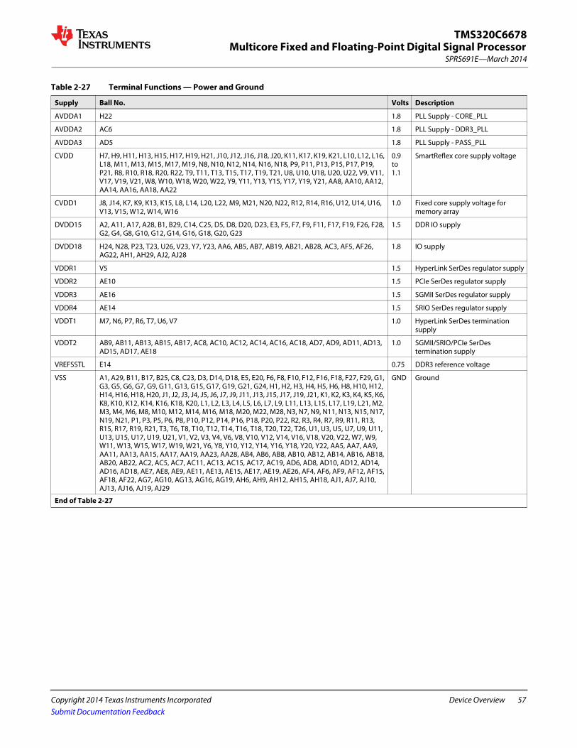
Multicore Fixed and Floating-Point Digital Signal Processor
Copyright 2014 Texas Instruments Incorporated Device Overview 57
SPRS691E—March 2014
TMS320C6678
Submit Documentation Feedback
Table 2-27 Terminal Functions — Power and Ground
Supply Ball No. Volts Description
AVDDA1 H22 1.8 PLL Supply - CORE_PLL
AVDDA2 AC6 1.8 PLL Supply - DDR3_PLL
AVDDA3 AD5 1.8 PLL Supply - PASS_PLL
CVDD H7, H9, H11, H13, H15, H17, H19, H21, J10, J12, J16, J18, J20, K11, K17, K19, K21, L10, L12, L16, L18, M11, M13, M15, M17, M19, N8, N10, N12, N14, N16, N18, P9, P11, P13, P15, P17, P19, P21, R8, R10, R18, R20, R22, T9, T11, T13, T15, T17, T19, T21, U8, U10, U18, U20, U22, V9, V11, V17, V19, V21, W8, W10, W18, W20, W22, Y9, Y11, Y13, Y15, Y17, Y19, Y21, AA8, AA10, AA12, AA14, AA16, AA18, AA22
0.9 to1.1
SmartReflex core supply voltage
CVDD1 J8, J14, K7, K9, K13, K15, L8, L14, L20, L22, M9, M21, N20, N22, R12, R14, R16, U12, U14, U16, V13, V15, W12, W14, W16
1.0 Fixed core supply voltage for memory array
DVDD15 A2, A11, A17, A28, B1, B29, C14, C25, D5, D8, D20, D23, E3, F5, F7, F9, F11, F17, F19, F26, F28, G2, G4, G8, G10, G12, G14, G16, G18, G20, G23
1.5 DDR IO supply
DVDD18 H24, N28, P23, T23, U26, V23, Y7, Y23, AA6, AB5, AB7, AB19, AB21, AB28, AC3, AF5, AF26, AG22, AH1, AH29, AJ2, AJ28
1.8 IO supply
VDDR1 V5 1.5 HyperLink SerDes regulator supply
VDDR2 AE10 1.5 PCIe SerDes regulator supply
VDDR3 AE16 1.5 SGMII SerDes regulator supply
VDDR4 AE14 1.5 SRIO SerDes regulator supply
VDDT1 M7, N6, P7, R6, T7, U6, V7 1.0 HyperLink SerDes termination supply
VDDT2 AB9, AB11, AB13, AB15, AB17, AC8, AC10, AC12, AC14, AC16, AC18, AD7, AD9, AD11, AD13, AD15, AD17, AE18
1.0 SGMII/SRIO/PCIe SerDes termination supply
VREFSSTL E14 0.75 DDR3 reference voltage
VSS A1, A29, B11, B17, B25, C8, C23, D3, D14, D18, E5, E20, F6, F8, F10, F12, F16, F18, F27, F29, G1, G3, G5, G6, G7, G9, G11, G13, G15, G17, G19, G21, G24, H1, H2, H3, H4, H5, H6, H8, H10, H12, H14, H16, H18, H20, J1, J2, J3, J4, J5, J6, J7, J9, J11, J13, J15, J17, J19, J21, K1, K2, K3, K4, K5, K6, K8, K10, K12, K14, K16, K18, K20, L1, L2, L3, L4, L5, L6, L7, L9, L11, L13, L15, L17, L19, L21, M2, M3, M4, M6, M8, M10, M12, M14, M16, M18, M20, M22, M28, N3, N7, N9, N11, N13, N15, N17, N19, N21, P1, P3, P5, P6, P8, P10, P12, P14, P16, P18, P20, P22, R2, R3, R4, R7, R9, R11, R13, R15, R17, R19, R21, T3, T6, T8, T10, T12, T14, T16, T18, T20, T22, T26, U1, U3, U5, U7, U9, U11, U13, U15, U17, U19, U21, V1, V2, V3, V4, V6, V8, V10, V12, V14, V16, V18, V20, V22, W7, W9, W11, W13, W15, W17, W19, W21, Y6, Y8, Y10, Y12, Y14, Y16, Y18, Y20, Y22, AA5, AA7, AA9, AA11, AA13, AA15, AA17, AA19, AA23, AA28, AB4, AB6, AB8, AB10, AB12, AB14, AB16, AB18, AB20, AB22, AC2, AC5, AC7, AC11, AC13, AC15, AC17, AC19, AD6, AD8, AD10, AD12, AD14, AD16, AD18, AE7, AE8, AE9, AE11, AE13, AE15, AE17, AE19, AE26, AF4, AF6, AF9, AF12, AF15, AF18, AF22, AG7, AG10, AG13, AG16, AG19, AH6, AH9, AH12, AH15, AH18, AJ1, AJ7, AJ10, AJ13, AJ16, AJ19, AJ29
GND Ground
End of Table 2-27

Multicore Fixed and Floating-Point Digital Signal Processor
Copyright 2014 Texas Instruments Incorporated Device Overview 58
SPRS691E—March 2014
TMS320C6678
Submit Documentation Feedback
Table 2-28 Terminal Functions — By Signal Name (Sheet 1 of 13)
Signal Name Ball Number
AVDDA1 H22
AVDDA2 AC6
AVDDA3 AD5
BOOTCOMPLETE AE2
BOOTMODE00 † J28
BOOTMODE01† J29
BOOTMODE02 † J26
BOOTMODE03 † J25
BOOTMODE04 † J27
BOOTMODE05 † J24
BOOTMODE06 † K27
BOOTMODE07 † K28
BOOTMODE08 † K26
BOOTMODE09 † K29
BOOTMODE10 † L28
BOOTMODE11 † L29
BOOTMODE12 † K25
CLKA0 AF25
CLKA1 AJ23
CLKB0 AG25
CLKB1 AH23
CORECLKN AG4
CORECLKP AG3
CORESEL0 AF2
CORESEL1 AD4
CORESEL2 AE6
CORESEL3 AE5
CVDD H7, H9, H11, H13, H15, H17, H19, H21, J10, J12, J16, J18, J20, K11, K17, K19, K21, L10, L12, L16, L18, M11, M13, M15, M17, M19, N8, N10, N12, N14,
CVDD N16, N18, P9, P11, P13, P15, P17, P19, P21, R8, R10, R18, R20, R22, T9, T11, T13, T15, T17, T19, T21, U8, U10, U18, U20, U22, V9, V11, V17, V19, V21, W8,
CVDD W10, W18, W20, W22, Y9, Y11, Y13, Y15, Y17, Y19, Y21, AA8, AA10, AA12, AA14, AA16, AA18, AA22
CVDD1 J8, J14, K7, K9, K13, K15, L8, L14, L20, L22, M9, M21, N20, N22, R12, R14, R16, U12, U14, U16, V13, V15, W12, W14, W16
DDRA00 A14
DDRA01 B14
DDRA02 F14
DDRA03 F13
DDRA04 A15
DDRA05 C15
DDRA06 B15
DDRA07 D15
DDRA08 F15
DDRA09 E15
DDRA10 E16
DDRA11 D16
DDRA12 E17
DDRA13 C16
DDRA14 D17
DDRA15 C17
DDRBA0 A13
DDRBA1 B13
DDRBA2 C13
DDRCAS D12
DDRCB00 E19
DDRCB01 C20
DDRCB02 D19
DDRCB03 B20
DDRCB04 C19
DDRCB05 C18
DDRCB06 B18
DDRCB07 A18
DDRCE0 C11
DDRCE1 C12
DDRCKE0 D11
DDRCKE1 E18
DDRCLKN H29
Table 2-28 Terminal Functions — By Signal Name (Sheet 2 of 13)
Signal Name Ball Number
DDRCLKOUTN0 B12
DDRCLKOUTN1 B16
DDRCLKOUTP0 A12
DDRCLKOUTP1 A16
DDRCLKP G29
DDRD00 E28
DDRD01 D29
DDRD02 E27
DDRD03 D28
DDRD04 D27
DDRD05 B28
DDRD06 E26
DDRD07 F25
DDRD08 F24
DDRD09 E24
DDRD10 E25
DDRD11 D25
DDRD12 D26
DDRD13 C26
DDRD14 B26
DDRD15 A26
DDRD16 F23
DDRD17 F22
DDRD18 D24
DDRD19 E23
DDRD20 A23
DDRD21 B23
DDRD22 C24
DDRD23 E22
DDRD24 D21
DDRD25 F20
DDRD26 E21
DDRD27 F21
DDRD28 D22
DDRD29 C21
DDRD30 B22
DDRD31 C22
DDRD32 E10
DDRD33 D10
DDRD34 B10
DDRD35 D9
DDRD36 E9
Table 2-28 Terminal Functions — By Signal Name (Sheet 3 of 13)
Signal Name Ball Number

59 Device Overview Copyright 2014 Texas Instruments Incorporated
SPRS691E—March 2014Multicore Fixed and Floating-Point Digital Signal ProcessorTMS320C6678
Submit Documentation Feedback
DDRD37 C9
DDRD38 B8
DDRD39 E8
DDRD40 A7
DDRD41 D7
DDRD42 E7
DDRD43 C7
DDRD44 B7
DDRD45 E6
DDRD46 D6
DDRD47 C6
DDRD48 C5
DDRD49 A5
DDRD50 B4
DDRD51 A4
DDRD52 D4
DDRD53 E4
DDRD54 C4
DDRD55 C3
DDRD56 F4
DDRD57 D2
DDRD58 E2
DDRD59 C2
DDRD60 F2
DDRD61 F3
DDRD62 E1
DDRD63 F1
DDRDQM0 E29
DDRDQM1 C27
DDRDQM2 A25
DDRDQM3 A22
DDRDQM4 A10
DDRDQM5 A8
DDRDQM6 B5
DDRDQM7 B2
DDRDQM8 A20
DDRDQS0N C29
DDRDQS0P C28
DDRDQS1N B27
DDRDQS1P A27
DDRDQS2N B24
DDRDQS2P A24
Table 2-28 Terminal Functions — By Signal Name (Sheet 4 of 13)
Signal Name Ball Number
DDRDQS3N B21
DDRDQS3P A21
DDRDQS4N B9
DDRDQS4P A9
DDRDQS5N A6
DDRDQS5P B6
DDRDQS6N A3
DDRDQS6P B3
DDRDQS7N C1
DDRDQS7P D1
DDRDQS8N B19
DDRDQS8P A19
DDRODT0 D13
DDRODT1 E13
DDRRAS C10
DDRRESET E11
DDRSLRATE0 G27
DDRSLRATE1 H27
DDRWE E12
DVDD15 A2, A11, A17, A28, B1, B29, C14, C25, D5, D8, D20, D23, E3, F5, F7, F9, F11, F17, F19, F26, F28, G2, G4, G8, G10, G12, G14, G16, G18, G20, G23
DVDD18 H24, N28, P23, T23, U26, V23, Y7, Y23, AA6, AB5, AB7, AB19, AB21, AB28, AC3, AF5, AF26, AG22, AH1, AH29, AJ2, AJ28
EMIFA00 T27
EMIFA01 T24
EMIFA02 U29
EMIFA03 T25
EMIFA04 U27
EMIFA05 U28
EMIFA06 U25
EMIFA07 U24
EMIFA08 V28
EMIFA09 V29
EMIFA10 V27
EMIFA11 V26
EMIFA12 V25
Table 2-28 Terminal Functions — By Signal Name (Sheet 5 of 13)
Signal Name Ball Number
EMIFA13 V24
EMIFA14 W28
EMIFA15 W27
EMIFA16 W29
EMIFA17 W26
EMIFA18 W25
EMIFA19 W24
EMIFA20 W23
EMIFA21 Y29
EMIFA22 Y28
EMIFA23 U23
EMIFBE0 R24
EMIFBE1 R23
EMIFCE0 P25
EMIFCE1 R27
EMIFCE2 R28
EMIFCE3 R25
EMIFD00 Y27
EMIFD01 AB29
EMIFD02 AA29
EMIFD03 Y26
EMIFD04 AA27
EMIFD05 AB27
EMIFD06 AA26
EMIFD07 AA25
EMIFD08 Y25
EMIFD09 AB25
EMIFD10 AA24
EMIFD11 Y24
EMIFD12 AB23
EMIFD13 AB24
EMIFD14 AB26
EMIFD15 AC25
EMIFOE R26
EMIFRW P26
EMIFWAIT0 T29
EMIFWAIT1 T28
EMIFWE P24
EMU00 AC29
EMU01 AC28
EMU02 AC27
EMU03 AC26
Table 2-28 Terminal Functions — By Signal Name (Sheet 6 of 13)
Signal Name Ball Number

Multicore Fixed and Floating-Point Digital Signal Processor
Copyright 2014 Texas Instruments Incorporated Device Overview 60
SPRS691E—March 2014
TMS320C6678
Submit Documentation Feedback
EMU04 AD29
EMU05 AD28
EMU06 AD27
EMU07 AE29
EMU08 AE28
EMU09 AF29
EMU10 AE27
EMU11 AF28
EMU12 AG29
EMU13 AD26
EMU14 AG28
EMU15 AG27
EMU16 AJ27
EMU17 AF27
EMU18 AH27
FSA0 AJ26
FSA1 AG23
FSB0 AG26
FSB1 AJ22
GPIO00 H25
GPIO01 J28
GPIO02 J29
GPIO03 J26
GPIO04 J25
GPIO05 J27
GPIO06 J24
GPIO07 K27
GPIO08 K28
GPIO09 K26
GPIO10 K29
GPIO11 L28
GPIO12 L29
GPIO13 K25
GPIO14 K24
GPIO15 L27
HOUT AD20
LENDIAN † H25
LRESETNMIEN M27
LRESET N26
MCMCLKN Y2
MCMCLKP W2
MCMREFCLKOUTN W1
Table 2-28 Terminal Functions — By Signal Name (Sheet 7 of 13)
Signal Name Ball Number
MCMREFCLKOUTP Y1
MCMRXFLCLK W3
MCMRXFLDAT W4
MCMRXN0 U2
MCMRXN1 T1
MCMRXN2 M1
MCMRXN3 P2
MCMRXP0 T2
MCMRXP1 R1
MCMRXP2 N1
MCMRXP3 N2
MCMRXPMCLK Y3
MCMRXPMDAT Y4
MCMTXFLCLK AA1
MCMTXFLDAT AA3
MCMTXN0 M5
MCMTXN1 T4
MCMTXN2 R5
MCMTXN3 N4
MCMTXP0 N5
MCMTXP1 U4
MCMTXP2 T5
MCMTXP3 P4
MCMTXPMCLK AA2
MCMTXPMDAT AA4
MDCLK H26
MDIO G26
NMI M25
PACLKSEL AE4
PASSCLKN AJ4
PASSCLKP AJ5
PCIECLKN AH5
PCIECLKP AG5
PCIERXN0 AH7
PCIERXN1 AJ9
PCIERXP0 AH8
PCIERXP1 AJ8
PCIESSMODE0 † K24
PCIESSMODE1 † L27
PCIESSEN † L24
PCIETXN0 AF8
PCIETXN1 AG9
Table 2-28 Terminal Functions — By Signal Name (Sheet 8 of 13)
Signal Name Ball Number
PCIETXP0 AF7
PCIETXP1 AG8
POR AC20
PTV15 G22
RESETFULL N25
RESETSTAT N27
RESET M29
RIORXN0 AJ11
RIORXN1 AH10
RIORXN2 AH14
RIORXN3 AJ15
RIORXP0 AJ12
RIORXP1 AH11
RIORXP2 AH13
RIORXP3 AJ14
RIOTXN0 AF10
RIOTXN1 AG11
RIOTXN2 AG15
RIOTXN3 AF14
RIOTXP0 AF11
RIOTXP1 AG12
RIOTXP2 AG14
RIOTXP3 AF13
RSV01 AH28
RSV02 N24
RSV03 N23
RSV04 AH2
RSV05 AJ3
RSV06 H28
RSV07 G28
RSV08 AH19
RSV09 AF19
RSV0A AA21
RSV0B AA20
RSV10 K22
RSV11 J22
RSV12 Y5
RSV13 W5
RSV14 W6
RSV15 AE12
RSV16 AC9
RSV17 AD19
Table 2-28 Terminal Functions — By Signal Name (Sheet 9 of 13)
Signal Name Ball Number

61 Device Overview Copyright 2014 Texas Instruments Incorporated
SPRS691E—March 2014Multicore Fixed and Floating-Point Digital Signal ProcessorTMS320C6678
Submit Documentation Feedback
RSV20 AF3
RSV21 G25
RSV22 AF1
RSV24 AH4
RSV25 AH3
SCL AD3
SDA AC4
SGMII0RXN AJ18
SGMII0RXP AJ17
SGMII0TXN AG18
SGMII0TXP AG17
SGMII1RXN AH17
SGMII1RXP AH16
SGMII1TXN AF17
SGMII1TXP AF16
SPICLK AE1
SPIDIN AD2
SPIDOUT AB1
SPISCS0 AG1
SPISCS1 AG2
SRIOSGMIICLKN AJ6
SRIOSGMIICLKP AG6
SYSCLKOUT AE3
TCK N29
TDI P27
TDO R29
TIMI0 L24
TIMI1 L26
TIMO0 L25
TIMO1 M26
TMS P29
TR00 AH26
TR01 AJ25
TR02 AD23
TR03 AD24
TR04 AC23
TR05 AH25
TR06 AC24
TR07 AE25
TR10 AE22
TR11 AD21
TR12 AC21
Table 2-28 Terminal Functions — By Signal Name (Sheet 10 of 13)
Signal Name Ball Number
TR13 AJ21
TR14 AH22
TR15 AJ20
TR16 AH21
TR17 AG21
TRST P28
TX00 AE24
TX01 AD25
TX02 AJ24
TX03 AG24
TX04 AH24
TX05 AF24
TX06 AE23
TX07 AF23
TX10 AF21
TX11 AD22
TX12 AC22
TX13 AE21
TX14 AG20
TX15 AE20
TX16 AH20
TX17 AF20
UARTCTS AB3
UARTRTS AB2
UARTRXD AD1
UARTTXD AC1
VCNTL0 L23
VCNTL1 K23
VCNTL2 J23
VCNTL3 H23
VDDR1 V5
VDDR2 AE10
VDDR3 AE16
VDDR4 AE14
VDDT1 M7, N6, P7, R6, T7, U6, V7
VDDT2 AB9, AB11, AB13, AB15, AB17, AC8, AC10, AC12, AC14, AC16, AC18, AD7, AD9, AD11, AD13, AD15, AD17, AE18
VREFSSTL E14
Table 2-28 Terminal Functions — By Signal Name (Sheet 11 of 13)
Signal Name Ball Number
VSS A1, A29, B11, B17, B25, C8, C23, D3, D14, D18, E5, E20, F6, F8, F10, F12, F16, F18, F27, F29, G1, G3, G5, G6, G7, G9, G11, G13, G15, G17, G19, G21, G24,
VSS H1, H2, H3, H4, H5, H6, H8, H10, H12, H14, H16, H18, H20, J1, J2, J3, J4, J5, J6, J7, J9, J11, J13, J15, J17, J19, J21, K1, K2, K3, K4, K5, K6, K8, K10, K12, K14, K16,
VSS K18, K20, L1, L2, L3, L4, L5, L6, L7, L9, L11, L13, L15, L17, L19, L21, M2, M3, M4, M6, M8, M10, M12, M14, M16, M18, M20, M22, M28, N3, N7, N9,
VSS N11, N13, N15, N17, N19, N21, P1, P3, P5, P6, P8, P10, P12, P14, P16, P18, P20, P22, R2, R3, R4, R7, R9, R11, R13, R15, R17, R19, R21, T3, T6, T8, T10, T12,
VSS T14, T16, T18, T20, T22, T26, U1, U3, U5, U7, U9, U11, U13, U15, U17, U19, U21, V1, V2, V3, V4, V6, V8, V10, V12, V14, V16, V18, V20, V22, W7, W9, W11,
VSS W13, W15, W17, W19, W21, Y6, Y8, Y10, Y12, Y14, Y16, Y18, Y20, Y22, AA5, AA7, AA9, AA11, AA13, AA15, AA17, AA19, AA23, AA28, AB4, AB6, AB8,
VSS AB10, AB12, AB14, AB16, AB18, AB20, AB22, AC2, AC5, AC7, AC11, AC13, AC15, AC17, AC19, AD6, AD8, AD10, AD12, AD14, AD16, AD18, AE7, AE8,
Table 2-28 Terminal Functions — By Signal Name (Sheet 12 of 13)
Signal Name Ball Number

Multicore Fixed and Floating-Point Digital Signal Processor
Copyright 2014 Texas Instruments Incorporated Device Overview 62
SPRS691E—March 2014
TMS320C6678
Submit Documentation Feedback
VSS AE9, AE11, AE13, AE15, AE17, AE19, AE26, AF4, AF6, AF9, AF12, AF15, AF18, AF22AG7, AG10, AG13, AG16, AG19, AH6, AH9, AH12, AH15, AH18,
VSS AJ1, AJ7, AJ10, AJ13, AJ16, AJ19, AJ29
End of Table 2-28
Table 2-28 Terminal Functions — By Signal Name (Sheet 13 of 13)
Signal Name Ball Number
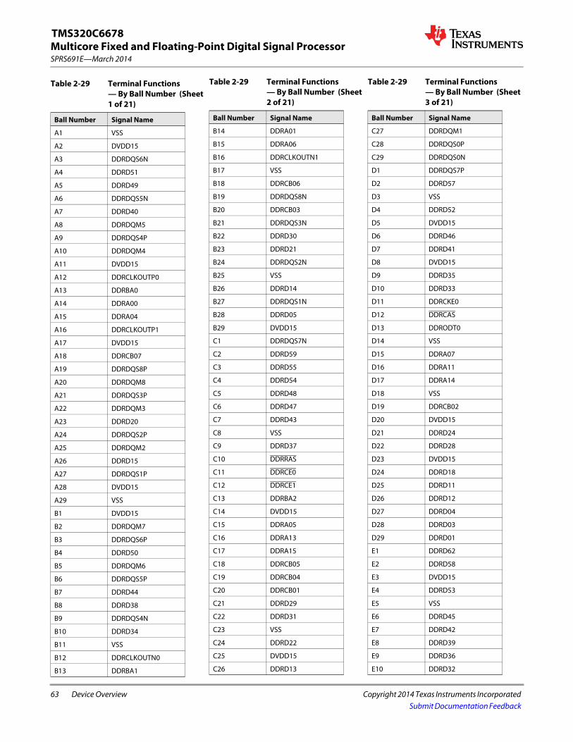
63 Device Overview Copyright 2014 Texas Instruments Incorporated
SPRS691E—March 2014Multicore Fixed and Floating-Point Digital Signal ProcessorTMS320C6678
Submit Documentation Feedback
Table 2-29 Terminal Functions — By Ball Number (Sheet 1 of 21)
Ball Number Signal Name
A1 VSS
A2 DVDD15
A3 DDRDQS6N
A4 DDRD51
A5 DDRD49
A6 DDRDQS5N
A7 DDRD40
A8 DDRDQM5
A9 DDRDQS4P
A10 DDRDQM4
A11 DVDD15
A12 DDRCLKOUTP0
A13 DDRBA0
A14 DDRA00
A15 DDRA04
A16 DDRCLKOUTP1
A17 DVDD15
A18 DDRCB07
A19 DDRDQS8P
A20 DDRDQM8
A21 DDRDQS3P
A22 DDRDQM3
A23 DDRD20
A24 DDRDQS2P
A25 DDRDQM2
A26 DDRD15
A27 DDRDQS1P
A28 DVDD15
A29 VSS
B1 DVDD15
B2 DDRDQM7
B3 DDRDQS6P
B4 DDRD50
B5 DDRDQM6
B6 DDRDQS5P
B7 DDRD44
B8 DDRD38
B9 DDRDQS4N
B10 DDRD34
B11 VSS
B12 DDRCLKOUTN0
B13 DDRBA1
B14 DDRA01
B15 DDRA06
B16 DDRCLKOUTN1
B17 VSS
B18 DDRCB06
B19 DDRDQS8N
B20 DDRCB03
B21 DDRDQS3N
B22 DDRD30
B23 DDRD21
B24 DDRDQS2N
B25 VSS
B26 DDRD14
B27 DDRDQS1N
B28 DDRD05
B29 DVDD15
C1 DDRDQS7N
C2 DDRD59
C3 DDRD55
C4 DDRD54
C5 DDRD48
C6 DDRD47
C7 DDRD43
C8 VSS
C9 DDRD37
C10 DDRRAS
C11 DDRCE0
C12 DDRCE1
C13 DDRBA2
C14 DVDD15
C15 DDRA05
C16 DDRA13
C17 DDRA15
C18 DDRCB05
C19 DDRCB04
C20 DDRCB01
C21 DDRD29
C22 DDRD31
C23 VSS
C24 DDRD22
C25 DVDD15
C26 DDRD13
Table 2-29 Terminal Functions — By Ball Number (Sheet 2 of 21)
Ball Number Signal Name
C27 DDRDQM1
C28 DDRDQS0P
C29 DDRDQS0N
D1 DDRDQS7P
D2 DDRD57
D3 VSS
D4 DDRD52
D5 DVDD15
D6 DDRD46
D7 DDRD41
D8 DVDD15
D9 DDRD35
D10 DDRD33
D11 DDRCKE0
D12 DDRCAS
D13 DDRODT0
D14 VSS
D15 DDRA07
D16 DDRA11
D17 DDRA14
D18 VSS
D19 DDRCB02
D20 DVDD15
D21 DDRD24
D22 DDRD28
D23 DVDD15
D24 DDRD18
D25 DDRD11
D26 DDRD12
D27 DDRD04
D28 DDRD03
D29 DDRD01
E1 DDRD62
E2 DDRD58
E3 DVDD15
E4 DDRD53
E5 VSS
E6 DDRD45
E7 DDRD42
E8 DDRD39
E9 DDRD36
E10 DDRD32
Table 2-29 Terminal Functions — By Ball Number (Sheet 3 of 21)
Ball Number Signal Name
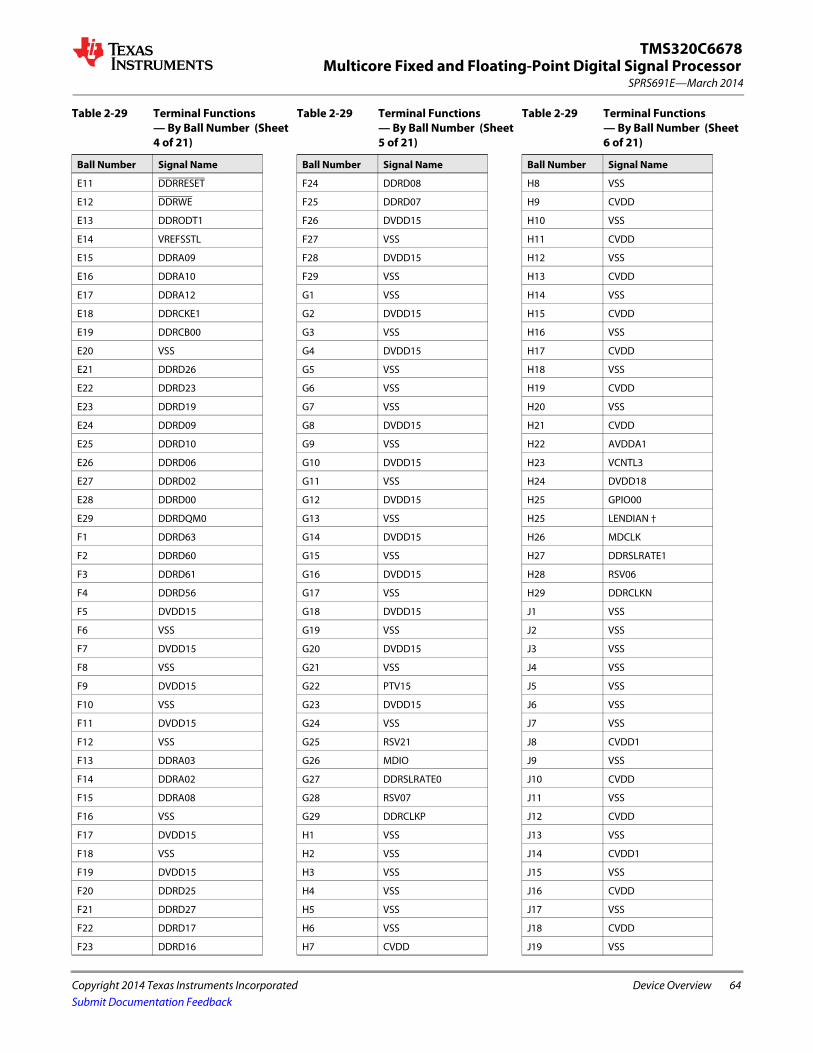
Multicore Fixed and Floating-Point Digital Signal Processor
Copyright 2014 Texas Instruments Incorporated Device Overview 64
SPRS691E—March 2014
TMS320C6678
Submit Documentation Feedback
E11 DDRRESET
E12 DDRWE
E13 DDRODT1
E14 VREFSSTL
E15 DDRA09
E16 DDRA10
E17 DDRA12
E18 DDRCKE1
E19 DDRCB00
E20 VSS
E21 DDRD26
E22 DDRD23
E23 DDRD19
E24 DDRD09
E25 DDRD10
E26 DDRD06
E27 DDRD02
E28 DDRD00
E29 DDRDQM0
F1 DDRD63
F2 DDRD60
F3 DDRD61
F4 DDRD56
F5 DVDD15
F6 VSS
F7 DVDD15
F8 VSS
F9 DVDD15
F10 VSS
F11 DVDD15
F12 VSS
F13 DDRA03
F14 DDRA02
F15 DDRA08
F16 VSS
F17 DVDD15
F18 VSS
F19 DVDD15
F20 DDRD25
F21 DDRD27
F22 DDRD17
F23 DDRD16
Table 2-29 Terminal Functions — By Ball Number (Sheet 4 of 21)
Ball Number Signal Name
F24 DDRD08
F25 DDRD07
F26 DVDD15
F27 VSS
F28 DVDD15
F29 VSS
G1 VSS
G2 DVDD15
G3 VSS
G4 DVDD15
G5 VSS
G6 VSS
G7 VSS
G8 DVDD15
G9 VSS
G10 DVDD15
G11 VSS
G12 DVDD15
G13 VSS
G14 DVDD15
G15 VSS
G16 DVDD15
G17 VSS
G18 DVDD15
G19 VSS
G20 DVDD15
G21 VSS
G22 PTV15
G23 DVDD15
G24 VSS
G25 RSV21
G26 MDIO
G27 DDRSLRATE0
G28 RSV07
G29 DDRCLKP
H1 VSS
H2 VSS
H3 VSS
H4 VSS
H5 VSS
H6 VSS
H7 CVDD
Table 2-29 Terminal Functions — By Ball Number (Sheet 5 of 21)
Ball Number Signal Name
H8 VSS
H9 CVDD
H10 VSS
H11 CVDD
H12 VSS
H13 CVDD
H14 VSS
H15 CVDD
H16 VSS
H17 CVDD
H18 VSS
H19 CVDD
H20 VSS
H21 CVDD
H22 AVDDA1
H23 VCNTL3
H24 DVDD18
H25 GPIO00
H25 LENDIAN †
H26 MDCLK
H27 DDRSLRATE1
H28 RSV06
H29 DDRCLKN
J1 VSS
J2 VSS
J3 VSS
J4 VSS
J5 VSS
J6 VSS
J7 VSS
J8 CVDD1
J9 VSS
J10 CVDD
J11 VSS
J12 CVDD
J13 VSS
J14 CVDD1
J15 VSS
J16 CVDD
J17 VSS
J18 CVDD
J19 VSS
Table 2-29 Terminal Functions — By Ball Number (Sheet 6 of 21)
Ball Number Signal Name
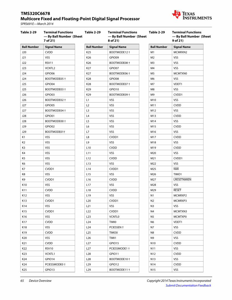
65 Device Overview Copyright 2014 Texas Instruments Incorporated
SPRS691E—March 2014Multicore Fixed and Floating-Point Digital Signal ProcessorTMS320C6678
Submit Documentation Feedback
J20 CVDD
J21 VSS
J22 RSV11
J23 VCNTL2
J24 GPIO06
J24 BOOTMODE05 †
J25 GPIO04
J25 BOOTMODE03 †
J26 GPIO03
J26 BOOTMODE02 †
J27 GPIO05
J27 BOOTMODE04 †
J28 GPIO01
J28 BOOTMODE00 †
J29 GPIO02
J29 BOOTMODE01†
K1 VSS
K2 VSS
K3 VSS
K4 VSS
K5 VSS
K6 VSS
K7 CVDD1
K8 VSS
K9 CVDD1
K10 VSS
K11 CVDD
K12 VSS
K13 CVDD1
K14 VSS
K15 CVDD1
K16 VSS
K17 CVDD
K18 VSS
K19 CVDD
K20 VSS
K21 CVDD
K22 RSV10
K23 VCNTL1
K24 GPIO14
K24 PCIESSMODE0 †
K25 GPIO13
Table 2-29 Terminal Functions — By Ball Number (Sheet 7 of 21)
Ball Number Signal Name
K25 BOOTMODE12 †
K26 GPIO09
K26 BOOTMODE08 †
K27 GPIO07
K27 BOOTMODE06 †
K28 GPIO08
K28 BOOTMODE07 †
K29 GPIO10
K29 BOOTMODE09 †
L1 VSS
L2 VSS
L3 VSS
L4 VSS
L5 VSS
L6 VSS
L7 VSS
L8 CVDD1
L9 VSS
L10 CVDD
L11 VSS
L12 CVDD
L13 VSS
L14 CVDD1
L15 VSS
L16 CVDD
L17 VSS
L18 CVDD
L19 VSS
L20 CVDD1
L21 VSS
L22 CVDD1
L23 VCNTL0
L24 TIMI0
L24 PCIESSEN †
L25 TIMO0
L26 TIMI1
L27 GPIO15
L27 PCIESSMODE1 †
L28 GPIO11
L28 BOOTMODE10 †
L29 GPIO12
L29 BOOTMODE11 †
Table 2-29 Terminal Functions — By Ball Number (Sheet 8 of 21)
Ball Number Signal Name
M1 MCMRXN2
M2 VSS
M3 VSS
M4 VSS
M5 MCMTXN0
M6 VSS
M7 VDDT1
M8 VSS
M9 CVDD1
M10 VSS
M11 CVDD
M12 VSS
M13 CVDD
M14 VSS
M15 CVDD
M16 VSS
M17 CVDD
M18 VSS
M19 CVDD
M20 VSS
M21 CVDD1
M22 VSS
M25 NMI
M26 TIMO1
M27 LRESETNMIEN
M28 VSS
M29 RESET
N1 MCMRXP2
N2 MCMRXP3
N3 VSS
N4 MCMTXN3
N5 MCMTXP0
N6 VDDT1
N7 VSS
N8 CVDD
N9 VSS
N10 CVDD
N11 VSS
N12 CVDD
N13 VSS
N14 CVDD
N15 VSS
Table 2-29 Terminal Functions — By Ball Number (Sheet 9 of 21)
Ball Number Signal Name
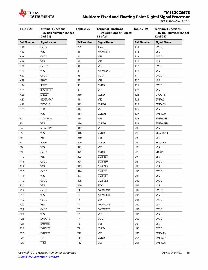
Multicore Fixed and Floating-Point Digital Signal Processor
Copyright 2014 Texas Instruments Incorporated Device Overview 66
SPRS691E—March 2014
TMS320C6678
Submit Documentation Feedback
N16 CVDD
N17 VSS
N18 CVDD
N19 VSS
N20 CVDD1
N21 VSS
N22 CVDD1
N23 RSV03
N24 RSV02
N25 RESETFULL
N26 LRESET
N27 RESETSTAT
N28 DVDD18
N29 TCK
P1 VSS
P2 MCMRXN3
P3 VSS
P4 MCMTXP3
P5 VSS
P6 VSS
P7 VDDT1
P8 VSS
P9 CVDD
P10 VSS
P11 CVDD
P12 VSS
P13 CVDD
P14 VSS
P15 CVDD
P16 VSS
P17 CVDD
P18 VSS
P19 CVDD
P20 VSS
P21 CVDD
P22 VSS
P23 DVDD18
P24 EMIFWE
P25 EMIFCE0
P26 EMIFRW
P27 TDI
P28 TRST
Table 2-29 Terminal Functions — By Ball Number (Sheet 10 of 21)
Ball Number Signal Name
P29 TMS
R1 MCMRXP1
R2 VSS
R3 VSS
R4 VSS
R5 MCMTXN2
R6 VDDT1
R7 VSS
R8 CVDD
R9 VSS
R10 CVDD
R11 VSS
R12 CVDD1
R13 VSS
R14 CVDD1
R15 VSS
R16 CVDD1
R17 VSS
R18 CVDD
R19 VSS
R20 CVDD
R21 VSS
R22 CVDD
R23 EMIFBE1
R24 EMIFBE0
R25 EMIFCE3
R26 EMIFOE
R27 EMIFCE1
R28 EMIFCE2
R29 TDO
T1 MCMRXN1
T2 MCMRXP0
T3 VSS
T4 MCMTXN1
T5 MCMTXP2
T6 VSS
T7 VDDT1
T8 VSS
T9 CVDD
T10 VSS
T11 CVDD
T12 VSS
Table 2-29 Terminal Functions — By Ball Number (Sheet 11 of 21)
Ball Number Signal Name
T13 CVDD
T14 VSS
T15 CVDD
T16 VSS
T17 CVDD
T18 VSS
T19 CVDD
T20 VSS
T21 CVDD
T22 VSS
T23 DVDD18
T24 EMIFA01
T25 EMIFA03
T26 VSS
T27 EMIFA00
T28 EMIFWAIT1
T29 EMIFWAIT0
U1 VSS
U2 MCMRXN0
U3 VSS
U4 MCMTXP1
U5 VSS
U6 VDDT1
U7 VSS
U8 CVDD
U9 VSS
U10 CVDD
U11 VSS
U12 CVDD1
U13 VSS
U14 CVDD1
U15 VSS
U16 CVDD1
U17 VSS
U18 CVDD
U19 VSS
U20 CVDD
U21 VSS
U22 CVDD
U23 EMIFA23
U24 EMIFA07
U25 EMIFA06
Table 2-29 Terminal Functions — By Ball Number (Sheet 12 of 21)
Ball Number Signal Name

67 Device Overview Copyright 2014 Texas Instruments Incorporated
SPRS691E—March 2014Multicore Fixed and Floating-Point Digital Signal ProcessorTMS320C6678
Submit Documentation Feedback
U26 DVDD18
U27 EMIFA04
U28 EMIFA05
U29 EMIFA02
V1 VSS
V2 VSS
V3 VSS
V4 VSS
V5 VDDR1
V6 VSS
V7 VDDT1
V8 VSS
V9 CVDD
V10 VSS
V11 CVDD
V12 VSS
V13 CVDD1
V14 VSS
V15 CVDD1
V16 VSS
V17 CVDD
V18 VSS
V19 CVDD
V20 VSS
V21 CVDD
V22 VSS
V23 DVDD18
V24 EMIFA13
V25 EMIFA12
V26 EMIFA11
V27 EMIFA10
V28 EMIFA08
V29 EMIFA09
W1 MCMREFCLKOUTN
W2 MCMCLKP
W3 MCMRXFLCLK
W4 MCMRXFLDAT
W5 RSV13
W6 RSV14
W7 VSS
W8 CVDD
W9 VSS
Table 2-29 Terminal Functions — By Ball Number (Sheet 13 of 21)
Ball Number Signal Name
W10 CVDD
W11 VSS
W12 CVDD1
W13 VSS
W14 CVDD1
W15 VSS
W16 CVDD1
W17 VSS
W18 CVDD
W19 VSS
W20 CVDD
W21 VSS
W22 CVDD
W23 EMIFA20
W24 EMIFA19
W25 EMIFA18
W26 EMIFA17
W27 EMIFA15
W28 EMIFA14
W29 EMIFA16
Y1 MCMREFCLKOUTP
Y2 MCMCLKN
Y3 MCMRXPMCLK
Y4 MCMRXPMDAT
Y5 RSV12
Y6 VSS
Y7 DVDD18
Y8 VSS
Y9 CVDD
Y10 VSS
Y11 CVDD
Y12 VSS
Y13 CVDD
Y14 VSS
Y15 CVDD
Y16 VSS
Y17 CVDD
Y18 VSS
Y19 CVDD
Y20 VSS
Y21 CVDD
Y22 VSS
Table 2-29 Terminal Functions — By Ball Number (Sheet 14 of 21)
Ball Number Signal Name
Y23 DVDD18
Y24 EMIFD11
Y25 EMIFD08
Y26 EMIFD03
Y27 EMIFD00
Y28 EMIFA22
Y29 EMIFA21
AA1 MCMTXFLCLK
AA2 MCMTXPMCLK
AA3 MCMTXFLDAT
AA4 MCMTXPMDAT
AA5 VSS
AA6 DVDD18
AA7 VSS
AA8 CVDD
AA9 VSS
AA10 CVDD
AA11 VSS
AA12 CVDD
AA13 VSS
AA14 CVDD
AA15 VSS
AA16 CVDD
AA17 VSS
AA18 CVDD
AA19 VSS
AA20 RSV0B
AA21 RSV0A
AA22 CVDD
AA23 VSS
AA24 EMIFD10
AA25 EMIFD07
AA26 EMIFD06
AA27 EMIFD04
AA28 VSS
AA29 EMIFD02
AB1 SPIDOUT
AB2 UARTRTS
AB3 UARTCTS
AB4 VSS
AB5 DVDD18
AB6 VSS
Table 2-29 Terminal Functions — By Ball Number (Sheet 15 of 21)
Ball Number Signal Name
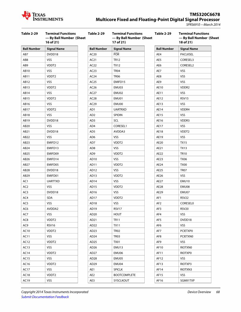
Multicore Fixed and Floating-Point Digital Signal Processor
Copyright 2014 Texas Instruments Incorporated Device Overview 68
SPRS691E—March 2014
TMS320C6678
Submit Documentation Feedback
AB7 DVDD18
AB8 VSS
AB9 VDDT2
AB10 VSS
AB11 VDDT2
AB12 VSS
AB13 VDDT2
AB14 VSS
AB15 VDDT2
AB16 VSS
AB17 VDDT2
AB18 VSS
AB19 DVDD18
AB20 VSS
AB21 DVDD18
AB22 VSS
AB23 EMIFD12
AB24 EMIFD13
AB25 EMIFD09
AB26 EMIFD14
AB27 EMIFD05
AB28 DVDD18
AB29 EMIFD01
AC1 UARTTXD
AC2 VSS
AC3 DVDD18
AC4 SDA
AC5 VSS
AC6 AVDDA2
AC7 VSS
AC8 VDDT2
AC9 RSV16
AC10 VDDT2
AC11 VSS
AC12 VDDT2
AC13 VSS
AC14 VDDT2
AC15 VSS
AC16 VDDT2
AC17 VSS
AC18 VDDT2
AC19 VSS
Table 2-29 Terminal Functions — By Ball Number (Sheet 16 of 21)
Ball Number Signal Name
AC20 POR
AC21 TR12
AC22 TX12
AC23 TR04
AC24 TR06
AC25 EMIFD15
AC26 EMU03
AC27 EMU02
AC28 EMU01
AC29 EMU00
AD1 UARTRXD
AD2 SPIDIN
AD3 SCL
AD4 CORESEL1
AD5 AVDDA3
AD6 VSS
AD7 VDDT2
AD8 VSS
AD9 VDDT2
AD10 VSS
AD11 VDDT2
AD12 VSS
AD13 VDDT2
AD14 VSS
AD15 VDDT2
AD16 VSS
AD17 VDDT2
AD18 VSS
AD19 RSV17
AD20 HOUT
AD21 TR11
AD22 TX11
AD23 TR02
AD24 TR03
AD25 TX01
AD26 EMU13
AD27 EMU06
AD28 EMU05
AD29 EMU04
AE1 SPICLK
AE2 BOOTCOMPLETE
AE3 SYSCLKOUT
Table 2-29 Terminal Functions — By Ball Number (Sheet 17 of 21)
Ball Number Signal Name
AE4 PACLKSEL
AE5 CORESEL3
AE6 CORESEL2
AE7 VSS
AE8 VSS
AE9 VSS
AE10 VDDR2
AE11 VSS
AE12 RSV15
AE13 VSS
AE14 VDDR4
AE15 VSS
AE16 VDDR3
AE17 VSS
AE18 VDDT2
AE19 VSS
AE20 TX15
AE21 TX13
AE22 TR10
AE23 TX06
AE24 TX00
AE25 TR07
AE26 VSS
AE27 EMU10
AE28 EMU08
AE29 EMU07
AF1 RSV22
AF2 CORESEL0
AF3 RSV20
AF4 VSS
AF5 DVDD18
AF6 VSS
AF7 PCIETXP0
AF8 PCIETXN0
AF9 VSS
AF10 RIOTXN0
AF11 RIOTXP0
AF12 VSS
AF13 RIOTXP3
AF14 RIOTXN3
AF15 VSS
AF16 SGMII1TXP
Table 2-29 Terminal Functions — By Ball Number (Sheet 18 of 21)
Ball Number Signal Name

69 Device Overview Copyright 2014 Texas Instruments Incorporated
SPRS691E—March 2014Multicore Fixed and Floating-Point Digital Signal ProcessorTMS320C6678
Submit Documentation Feedback
AF17 SGMII1TXN
AF18 VSS
AF19 RSV09
AF20 TX17
AF21 TX10
AF22 VSS
AF23 TX07
AF24 TX05
AF25 CLKA0
AF26 DVDD18
AF27 EMU17
AF28 EMU11
AF29 EMU09
AG1 SPISCS0
AG2 SPISCS1
AG3 CORECLKP
AG4 CORECLKN
AG5 PCIECLKP
AG6 SRIOSGMIICLKP
AG7 VSS
AG8 PCIETXP1
AG9 PCIETXN1
AG10 VSS
AG11 RIOTXN1
AG12 RIOTXP1
AG13 VSS
AG14 RIOTXP2
AG15 RIOTXN2
AG16 VSS
AG17 SGMII0TXP
AG18 SGMII0TXN
AG19 VSS
AG20 TX14
AG21 TR17
AG22 DVDD18
AG23 FSA1
AG24 TX03
AG25 CLKB0
AG26 FSB0
AG27 EMU15
AG28 EMU14
AG29 EMU12
Table 2-29 Terminal Functions — By Ball Number (Sheet 19 of 21)
Ball Number Signal Name
AH1 DVDD18
AH2 RSV04
AH3 RSV25
AH4 RSV24
AH5 PCIECLKN
AH6 VSS
AH7 PCIERXN0
AH8 PCIERXP0
AH9 VSS
AH10 RIORXN1
AH11 RIORXP1
AH12 VSS
AH13 RIORXP2
AH14 RIORXN2
AH15 VSS
AH16 SGMII1RXP
AH17 SGMII1RXN
AH18 VSS
AH19 RSV08
AH20 TX16
AH21 TR16
AH22 TR14
AH23 CLKB1
AH24 TX04
AH25 TR05
AH26 TR00
AH27 EMU18
AH28 RSV01
AH29 DVDD18
AJ1 VSS
AJ2 DVDD18
AJ3 RSV05
AJ4 PASSCLKN
AJ5 PASSCLKP
AJ6 SRIOSGMIICLKN
AJ7 VSS
AJ8 PCIERXP1
AJ9 PCIERXN1
AJ10 VSS
AJ11 RIORXN0
AJ12 RIORXP0
AJ13 VSS
Table 2-29 Terminal Functions — By Ball Number (Sheet 20 of 21)
Ball Number Signal Name
AJ14 RIORXP3
AJ15 RIORXN3
AJ16 VSS
AJ17 SGMII0RXP
AJ18 SGMII0RXN
AJ19 VSS
AJ20 TR15
AJ21 TR13
AJ22 FSB1
AJ23 CLKA1
AJ24 TX02
AJ25 TR01
AJ26 FSA0
AJ27 EMU16
AJ28 DVDD18
AJ29 VSS
End of Table 2-29
Table 2-29 Terminal Functions — By Ball Number (Sheet 21 of 21)
Ball Number Signal Name

70 Device Overview Copyright 2014 Texas Instruments Incorporated
SPRS691E—March 2014Multicore Fixed and Floating-Point Digital Signal ProcessorTMS320C6678
Submit Documentation Feedback
2.9 Development and Support2.9.1 Development Support
In case the customer would like to develop their own features and software on the C6678 device, TI offers an extensive line of development tools for the TMS320C6000™ DSP platform, including tools to evaluate the performance of the processors, generate code, develop algorithm implementations, and fully integrate and debug software and hardware modules. The tool's support documentation is electronically available within the Code Composer Studio™ Integrated Development Environment (IDE).
The following products support development of C6000™ DSP-based applications:• Software Development Tools:
– Code Composer Studio™ Integrated Development Environment (IDE), including Editor C/C++/Assembly Code Generation, and Debug plus additional development tools.
– Scalable, Real-Time Foundation Software (DSP/BIOS™), which provides the basic run-time target software needed to support any DSP application.
• Hardware Development Tools: – Extended Development System (XDS™) Emulator (supports C6000™ DSP multiprocessor system debug) – EVM (Evaluation Module)
2.9.2 Device Support
2.9.2.1 Device and Development-Support Tool Nomenclature
To designate the stages in the product development cycle, TI assigns prefixes to the part numbers of all DSP devices and support tools. Each DSP commercial family member has one of three prefixes: TMX, TMP, or TMS (e.g., TMX320CMH). Texas Instruments recommends two of three possible prefix designators for its support tools: TMDX and TMDS. These prefixes represent evolutionary stages of product development from engineering prototypes (TMX/TMDX) through fully qualified production devices/tools (TMS/TMDS).
Device development evolutionary flow:• TMX: Experimental device that is not necessarily representative of the final device's electrical specifications• TMP: Final silicon die that conforms to the device's electrical specifications but has not completed quality and
reliability verification• TMS: Fully qualified production device
Support tool development evolutionary flow:• TMDX: Development-support product that has not yet completed Texas Instruments internal qualification
testing.• TMDS: Fully qualified development-support product
TMX and TMP devices and TMDX development-support tools are shipped with the following disclaimer:"Developmental product is intended for internal evaluation purposes."
TMS devices and TMDS development-support tools have been characterized fully, and the quality and reliability of the device have been demonstrated fully. TI's standard warranty applies.
Predictions show that prototype devices (TMX or TMP) have a greater failure rate than the standard production devices. Texas Instruments recommends that these devices not be used in any production system because their expected end-use failure rate still is undefined. Only qualified production devices are to be used.
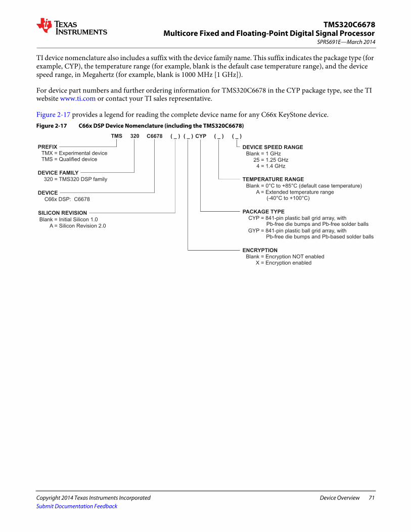
Multicore Fixed and Floating-Point Digital Signal Processor
Copyright 2014 Texas Instruments Incorporated Device Overview 71
SPRS691E—March 2014
TMS320C6678
Submit Documentation Feedback
TI device nomenclature also includes a suffix with the device family name. This suffix indicates the package type (for example, CYP), the temperature range (for example, blank is the default case temperature range), and the device speed range, in Megahertz (for example, blank is 1000 MHz [1 GHz]).
For device part numbers and further ordering information for TMS320C6678 in the CYP package type, see the TI website www.ti.com or contact your TI sales representative.
Figure 2-17 provides a legend for reading the complete device name for any C66x KeyStone device.Figure 2-17 C66x DSP Device Nomenclature (including the TMS320C6678)
C66x DSP: C6678
Blank = Initial Silicon 1.0
PREFIX
TMS 320 C6678 CYP
TMX = Experimental deviceTMS = Qualified device
DEVICE FAMILY
320 = TMS320 DSP family
DEVICE
DEVICE SPEED RANGE
( _ )
Blank = 1 GHz
( _ )
TEMPERATURE RANGE
PACKAGE TYPE
CYP = 841-pin plastic ball grid array, withand Pb-free solder ballsPb-free die bumps
A = Extended temperature range(-40°C to +100°C)
( _ )
SILICON REVISION
Blank = 0°C to +85°C (default case temperature)
( _ )
ENCRYPTIONBlank = Encryption NOT enabled
X = Encryption enabled
25 = 1.25 GHz
A = Silicon Revision 2.0GYP = 841-pin plastic ball grid array, with
Pb-free die bumps and Pb-based solder balls
4 = 1.4 GHz
72 Device Overview Copyright 2014 Texas Instruments Incorporated
SPRS691E—March 2014Multicore Fixed and Floating-Point Digital Signal ProcessorTMS320C6678
Submit Documentation Feedback
2.10 Related Documentation from Texas InstrumentsThese documents describe the TMS320C6678 Multicore Fixed and Floating-Point Digital Signal Processor. Copies of these documents are available on the Internet at www.ti.com
C66x DSP CorePac User Guide SPRUGW0
C66x DSP CPU and Instruction Set Reference Guide SPRUGH7
C66x DSP Cache User Guide SPRUGY8
Chip Interrupt Controller (CIC) for KeyStone Devices User Guide SPRUGW4
DDR3 Design Requirements for KeyStone Devices SPRABI1
DDR3 Memory Controller for KeyStone Devices User Guide SPRUGV8
Debug and Trace for KeyStone I Devices User Guide SPRUGZ2
DSP Bootloader for KeyStone Devices User Guide SPRUGY5
Emulation and Trace Headers Technical Reference SPRU655
Enhanced Direct Memory Access 3 (EDMA3) Controller for KeyStone Devices User Guide SPRUGS5
External Memory Interface (EMIF16) for KeyStone Devices User Guide SPRUGZ3
General Purpose Input/Output (GPIO) for KeyStone Devices User Guide SPRUGV1
Gigabit Ethernet (GbE) Switch Subsystem for KeyStone Devices User Guide SPRUGV9
Hardware Design Guide for KeyStone I Devices SPRABI2
HyperLink for KeyStone Devices User Guide SPRUGW8
Inter -IC Control Bus (I2C) for KeyStone Devices User Guide SPRUGV3
Memory Protection Unit (MPU) for KeyStone Devices User Guide SPRUGW5
Multicore Navigator for KeyStone Devices User Guide SPRUGR9
Multicore Shared Memory Controller (MSMC) for KeyStone Devices User Guide SPRUGW7
Network Coprocessor (NETCP) for KeyStone Devices User Guide SPRUGZ6
Packet Accelerator (PA) for KeyStone Devices User Guide SPRUGS4
Peripheral Component Interconnect Express (PCIe) for KeyStone Devices User Guide SPRUGS6
Phase Locked Loop (PLL) for KeyStone Devices User Guide SPRUGV2
Power Consumption Summary for KeyStone C66x Devices SPRABL5
Power Sleep Controller (PSC) for KeyStone Devices User Guide SPRUGV4
Security Accelerator (SA) for KeyStone Devices User Guide SPRUGY6
Semaphore2 Hardware Module for KeyStone Devices User Guide SPRUGS3
Serial Peripheral Interface (SPI) for KeyStone Devices User Guide SPRUGP2
Serial RapidIO (SRIO) for KeyStone Devices User Guide SPRUGW1
Telecom Serial Interface Port (TSIP) for the C66x DSP User Guide SPRUGY4
Timer64P for KeyStone Devices User Guide SPRUGV5
Universal Asynchronous Receiver/Transmitter (UART) for KeyStone Devices User Guide SPRUGP1
Using Advanced Event Triggering to Debug Real-Time Problems in High Speed Embedded Microprocessor Systems SPRA387
Using Advanced Event Triggering to Find and Fix Intermittent Real-Time Bugs SPRA753
Using IBIS Models for Timing Analysis SPRA839
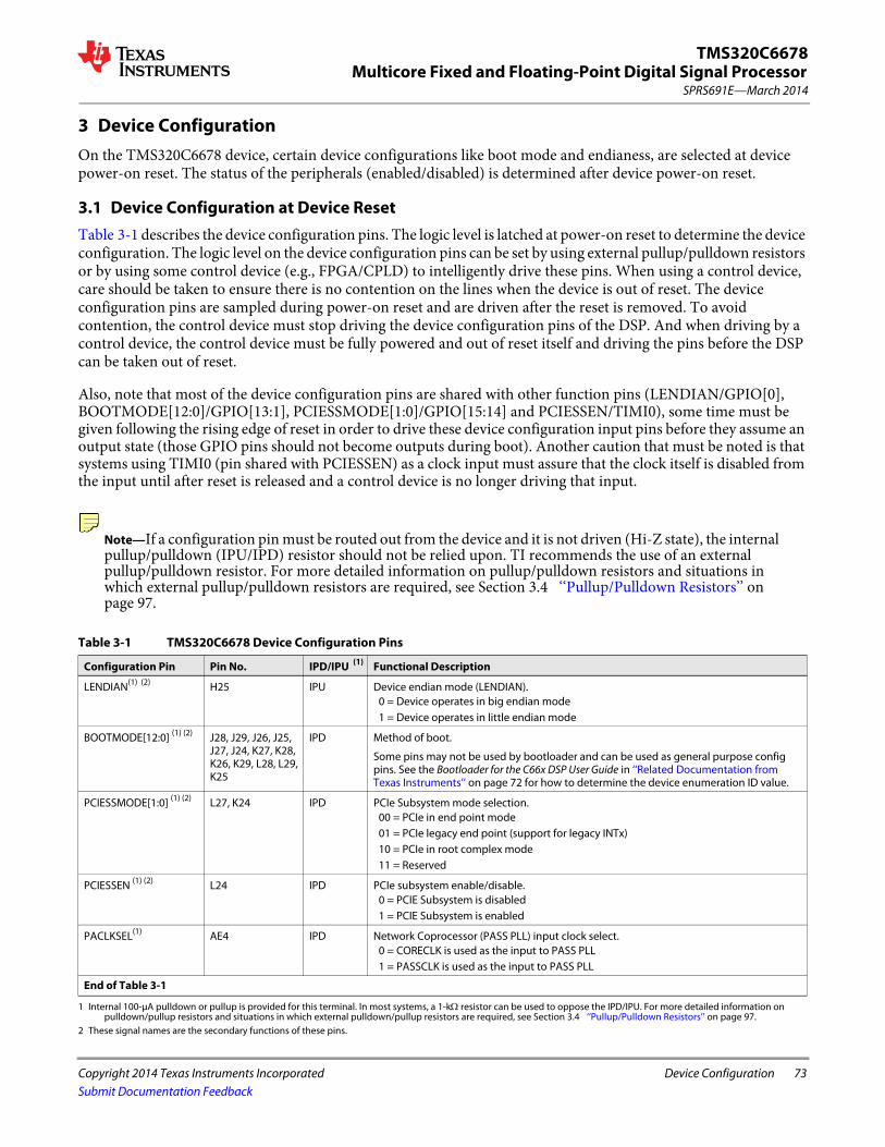
Multicore Fixed and Floating-Point Digital Signal Processor
Copyright 2014 Texas Instruments Incorporated Device Configuration 73
SPRS691E—March 2014
TMS320C6678
Submit Documentation Feedback
3 Device ConfigurationOn the TMS320C6678 device, certain device configurations like boot mode and endianess, are selected at device power-on reset. The status of the peripherals (enabled/disabled) is determined after device power-on reset.
3.1 Device Configuration at Device Reset Table 3-1 describes the device configuration pins. The logic level is latched at power-on reset to determine the device configuration. The logic level on the device configuration pins can be set by using external pullup/pulldown resistors or by using some control device (e.g., FPGA/CPLD) to intelligently drive these pins. When using a control device, care should be taken to ensure there is no contention on the lines when the device is out of reset. The device configuration pins are sampled during power-on reset and are driven after the reset is removed. To avoid contention, the control device must stop driving the device configuration pins of the DSP. And when driving by a control device, the control device must be fully powered and out of reset itself and driving the pins before the DSP can be taken out of reset.
Also, note that most of the device configuration pins are shared with other function pins (LENDIAN/GPIO[0], BOOTMODE[12:0]/GPIO[13:1], PCIESSMODE[1:0]/GPIO[15:14] and PCIESSEN/TIMI0), some time must be given following the rising edge of reset in order to drive these device configuration input pins before they assume an output state (those GPIO pins should not become outputs during boot). Another caution that must be noted is that systems using TIMI0 (pin shared with PCIESSEN) as a clock input must assure that the clock itself is disabled from the input until after reset is released and a control device is no longer driving that input.
Note—If a configuration pin must be routed out from the device and it is not driven (Hi-Z state), the internal pullup/pulldown (IPU/IPD) resistor should not be relied upon. TI recommends the use of an external pullup/pulldown resistor. For more detailed information on pullup/pulldown resistors and situations in which external pullup/pulldown resistors are required, see Section 3.4 ‘‘Pullup/Pulldown Resistors’’ on page 97.
Table 3-1 TMS320C6678 Device Configuration Pins
Configuration Pin Pin No. IPD/IPU (1)
1 Internal 100-μA pulldown or pullup is provided for this terminal. In most systems, a 1-k resistor can be used to oppose the IPD/IPU. For more detailed information on pulldown/pullup resistors and situations in which external pulldown/pullup resistors are required, see Section 3.4 ‘‘Pullup/Pulldown Resistors’’ on page 97.
Functional Description
LENDIAN(1) (2)
2 These signal names are the secondary functions of these pins.
H25 IPU Device endian mode (LENDIAN).0 = Device operates in big endian mode 1 = Device operates in little endian mode
BOOTMODE[12:0] (1) (2) J28, J29, J26, J25, J27, J24, K27, K28, K26, K29, L28, L29, K25
IPD Method of boot.
Some pins may not be used by bootloader and can be used as general purpose config pins. See the Bootloader for the C66x DSP User Guide in ‘‘Related Documentation from Texas Instruments’’ on page 72 for how to determine the device enumeration ID value.
PCIESSMODE[1:0] (1) (2) L27, K24 IPD PCIe Subsystem mode selection.00 = PCIe in end point mode01 = PCIe legacy end point (support for legacy INTx)10 = PCIe in root complex mode11 = Reserved
PCIESSEN (1) (2) L24 IPD PCIe subsystem enable/disable. 0 = PCIE Subsystem is disabled1 = PCIE Subsystem is enabled
PACLKSEL(1) AE4 IPD Network Coprocessor (PASS PLL) input clock select. 0 = CORECLK is used as the input to PASS PLL1 = PASSCLK is used as the input to PASS PLL
End of Table 3-1
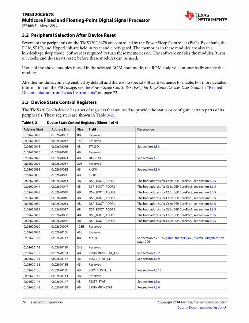
74 Device Configuration Copyright 2014 Texas Instruments Incorporated
SPRS691E—March 2014Multicore Fixed and Floating-Point Digital Signal ProcessorTMS320C6678
Submit Documentation Feedback
3.2 Peripheral Selection After Device ResetSeveral of the peripherals on the TMS320C6678 are controlled by the Power Sleep Controller (PSC). By default, the PCIe, SRIO, and HyperLink are held in reset and clock-gated. The memories in these modules are also in a low-leakage sleep mode. Software is required to turn these memories on. The software enables the modules (turns on clocks and de-asserts reset) before these modules can be used.
If one of the above modules is used in the selected ROM boot mode, the ROM code will automatically enable the module.
All other modules come up enabled by default and there is no special software sequence to enable. For more detailed information on the PSC usage, see the Power Sleep Controller (PSC) for KeyStone Devices User Guide in ‘‘Related Documentation from Texas Instruments’’ on page 72.
3.3 Device State Control RegistersThe TMS320C6678 device has a set of registers that are used to provide the status or configure certain parts of its peripherals. These registers are shown in Table 3-2.Table 3-2 Device State Control Registers (Sheet 1 of 4)
Address Start Address End Size Field Description
0x02620000 0x02620007 8B Reserved
0x02620008 0x02620017 16B Reserved
0x02620018 0x0262001B 4B JTAGID See section 3.3.3
0x0262001C 0x0262001F 4B Reserved
0x02620020 0x02620023 4B DEVSTAT See section 3.3.1
0x02620024 0x02620037 20B Reserved
0x02620038 0x0262003B 4B KICK0 See section 3.3.4
0x0262003C 0x0262003F 4B KICK1
0x02620040 0x02620043 4B DSP_BOOT_ADDR0 The boot address for C66x DSP CorePac0, see section 3.3.5
0x02620044 0x02620047 4B DSP_BOOT_ADDR1 The boot address for C66x DSP CorePac1, see section 3.3.5
0x02620048 0x0262004B 4B DSP_BOOT_ADDR2 The boot address for C66x DSP CorePac2, see section 3.3.5
0x0262004C 0x0262004F 4B DSP_BOOT_ADDR3 The boot address for C66x DSP CorePac3, see section 3.3.5
0x02620050 0x02620053 4B DSP_BOOT_ADDR4 The boot address for C66x DSP CorePac4, see section 3.3.5
0x02620054 0x02620057 4B DSP_BOOT_ADDR5 The boot address for C66x DSP CorePac5, see section 3.3.5
0x02620058 0x0262005B 4B DSP_BOOT_ADDR6 The boot address for C66x DSP CorePac6, see section 3.3.5
0x0262005C 0x0262005F 4B DSP_BOOT_ADDR7 The boot address for C66x DSP CorePac7, see section 3.3.5
0x02620060 0x026200DF 128B Reserved
0x026200E0 0x0262010F 48B Reserved
0x02620110 0x02620117 8B MACID See section 7.22 ‘‘Gigabit Ethernet (GbE) Switch Subsystem’’ on page 226
0x02620118 0x0262012F 24B Reserved
0x02620130 0x02620133 4B LRSTNMIPINSTAT_CLR See section 3.3.7
0x02620134 0x02620137 4B RESET_STAT_CLR See section 3.3.9
0x02620138 0x0262013B 4B Reserved
0x0262013C 0x0262013F 4B BOOTCOMPLETE See section 3.3.10
0x02620140 0x02620143 4B Reserved
0x02620144 0x02620147 4B RESET_STAT See section 3.3.8
0x02620148 0x0262014B 4B LRSTNMIPINSTAT See section 3.3.6

Multicore Fixed and Floating-Point Digital Signal Processor
Copyright 2014 Texas Instruments Incorporated Device Configuration 75
SPRS691E—March 2014
TMS320C6678
Submit Documentation Feedback
0x0262014C 0x0262014F 4B DEVCFG See section 3.3.2
0x02620150 0x02620153 4B PWRSTATECTL See section 3.3.11
0x02620154 0x02620157 4B SRIO_SERDES_STS See ‘‘Related Documentation from Texas Instruments’’ on page 72
0x02620158 0x0262015B 4B SMGII_SERDES_STS
0x0262015C 0x0262015F 4B PCIE_SERDES_STS
0x02620160 0x02620163 4B HYPERLINK_SERDES_STS
0x02620164 0x02620167 4B Reserved
0x02620168 0x0262016B 4B Reserved
0x0262016C 0x0262017F 20B Reserved
0x02620180 0x02620183 4B Reserved
0x02620184 0x0262018F 12B Reserved
0x02620190 0x02620193 4B Reserved
0x02620194 0x02620197 4B Reserved
0x02620198 0x0262019B 4B Reserved
0x0262019C 0x0262019F 4B Reserved
0x026201A0 0x026201A3 4B Reserved
0x026201A4 0x026201A7 4B Reserved
0x026201A8 0x026201AB 4B Reserved
0x026201AC 0x026201AF 4B Reserved
0x026201B0 0x026201B3 4B Reserved
0x026201B4 0x026201B7 4B Reserved
0x026201B8 0x026201BB 4B Reserved
0x026201BC 0x026201BF 4B Reserved
0x026201C0 0x026201C3 4B Reserved
0x026201C4 0x026201C7 4B Reserved
0x026201C8 0x026201CB 4B Reserved
0x026201CC 0x026201CF 4B Reserved
0x026201D0 0x026201FF 48B Reserved
0x02620200 0x02620203 4B NMIGR0 See section 3.3.12
0x02620204 0x02620207 4B NMIGR1
0x02620208 0x0262020B 4B NMIGR2
0x0262020C 0x0262020F 4B NMIGR3
0x02620210 0x02620213 4B NMIGR4
0x02620214 0x02620217 4B NMIGR5
0x02620218 0x0262021B 4B NMIGR6
0x0262021C 0x0262021F 4B NMIGR7
0x02620220 0x0262023F 32B Reserved
Table 3-2 Device State Control Registers (Sheet 2 of 4)
Address Start Address End Size Field Description

76 Device Configuration Copyright 2014 Texas Instruments Incorporated
SPRS691E—March 2014Multicore Fixed and Floating-Point Digital Signal ProcessorTMS320C6678
Submit Documentation Feedback
0x02620240 0x02620243 4B IPCGR0 See section 3.3.13
0x02620244 0x02620247 4B IPCGR1
0x02620248 0x0262024B 4B IPCGR2
0x0262024C 0x0262024F 4B IPCGR3
0x02620250 0x02620253 4B IPCGR4
0x02620254 0x02620257 4B IPCGR5
0x02620258 0x0262025B 4B IPCGR6
0x0262025C 0x0262025F 4B IPCGR7
0x02620260 0x0262027B 28B Reserved
0x0262027C 0x0262027F 4B IPCGRH See section 3.3.15
0x02620280 0x02620283 4B IPCAR0 See section 3.3.14
0x02620284 0x02620287 4B IPCAR1
0x02620288 0x0262028B 4B IPCAR2
0x0262028C 0x0262028F 4B IPCAR3
0x02620290 0x02620293 4B IPCAR4
0x02620294 0x02620297 4B IPCAR5
0x02620298 0x0262029B 4B IPCAR6
0x0262029C 0x0262029F 4B IPCAR7
0x026202A0 0x026202BB 28B Reserved
0x026202BC 0x026202BF 4B IPCARH See section 3.3.16
0x026202C0 0x026202FF 64B Reserved
0x02620300 0x02620303 4B TINPSEL See section 3.3.17
See section 3.3.180x02620304 0x02620307 4B TOUTPSEL
0x02620308 0x0262030B 4B RSTMUX0 See section 3.3.19
0x0262030C 0x0262030F 4B RSTMUX1
0x02620310 0x02620313 4B RSTMUX2
0x02620314 0x02620317 4B RSTMUX3
0x02620318 0x0262031B 4B RSTMUX4
0x0262031C 0x0262031F 4B RSTMUX5
0x02620320 0x02620323 4B RSTMUX6
0x02620324 0x02620327 4B RSTMUX7
0x02620328 0x0262032B 4B MAINPLLCTL0 See section 7.6 ‘‘Main PLL and PLL Controller’’ on page 140
0x0262032C 0x0262032F 4B MAINPLLCTL1
0x02620330 0x02620333 4B DDR3PLLCTL0 See section 7.7 ‘‘DD3 PLL’’ on page 153
0x02620334 0x02620337 4B DDR3PLLCTL1
0x02620338 0x0262033B 4B PASSPLLCTL0 See section 7.8 ‘‘PASS PLL’’ on page 156
0x0262033C 0x0262033F 4B PASSPLLCTL1
Table 3-2 Device State Control Registers (Sheet 3 of 4)
Address Start Address End Size Field Description

Multicore Fixed and Floating-Point Digital Signal Processor
Copyright 2014 Texas Instruments Incorporated Device Configuration 77
SPRS691E—March 2014
TMS320C6678
Submit Documentation Feedback
0x02620340 0x02620343 4B SGMII_SERDES_CFGPLL See ‘‘Related Documentation from Texas Instruments’’ on page 72
0x02620344 0x02620347 4B SGMII_SERDES_CFGRX0
0x02620348 0x0262034B 4B SGMII_SERDES_CFGTX0
0x0262034C 0x0262034F 4B SGMII_SERDES_CFGRX1
0x02620350 0x02620353 4B SGMII_SERDES_CFGTX1
0x02620354 0x02620357 4B Reserved
0x02620358 0x0262035B 4B PCIE_SERDES_CFGPLL
0x0262035C 0x0262035F 4B Reserved
0x02620360 0x02620363 4B SRIO_SERDES_CFGPLL
0x02620364 0x02620367 4B SRIO_SERDES_CFGRX0
0x02620368 0x0262036B 4B SRIO_SERDES_CFGTX0
0x0262036C 0x0262036F 4B SRIO_SERDES_CFGRX1
0x02620370 0x02620373 4B SRIO_SERDES_CFGTX1
0x02620374 0x02620377 4B SRIO_SERDES_CFGRX2
0x02620378 0x0262037B 4B SRIO_SERDES_CFGTX2
0x0262037C 0x0262037F 4B SRIO_SERDES_CFGRX3
0x02620380 0x02620383 4B SRIO_SERDES_CFGTX3
0x02620384 0x0262038B 8B Reserved
0x0262038C 0x0262038F 4B DSP_SUSP_CTL See section 3.3.20
0x02620390 0x026203B3 36B Reserved
0x026203B4 0x026203B7 4B HYPERLINK_SERDES_CFGPLL See ‘‘Related Documentation from Texas Instruments’’ on page 72
0x026203B8 0x026203BB 4B HYPERLINK_SERDES_CFGRX0
0x026203BC 0x026203BF 4B HYPERLINK_SERDES_CFGTX0
0x026203C0 0x026203C3 4B HYPERLINK_SERDES_CFGRX1
0x026203C4 0x026203C7 4B HYPERLINK_SERDES_CFGTX1
0x026203C8 0x026203CB 4B HYPERLINK_SERDES_CFGRX2
0x026203CC 0x026203CF 4B HYPERLINK_SERDES_CFGTX2
0x026203D0 0x026203D3 4B HYPERLINK_SERDES_CFGRX3
0x026203D4 0x026203D7 4B HYPERLINK_SERDES_CFGTX3
0x026203D8 0x026203DB 4B Reserved
0x026203DC 0x026203F7 28B Reserved
0x026203F8 0x026203FB 4B DEVSPEED See section 3.3.21
0x026203FC 0x026203FF 4B Reserved
0x02620400 0x02620403 4B CHIP_MISC_CTL See section 3.3.22
0x02620404 0x02620467 100B Reserved
End of Table 3-2
Table 3-2 Device State Control Registers (Sheet 4 of 4)
Address Start Address End Size Field Description
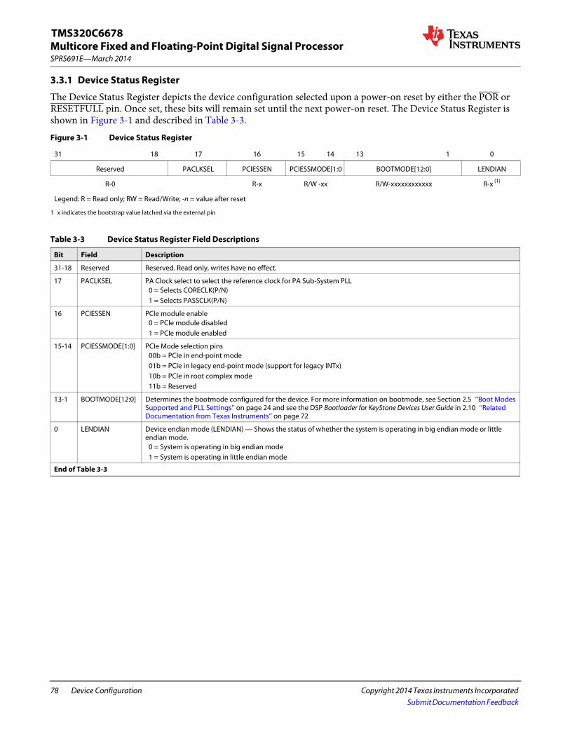
78 Device Configuration Copyright 2014 Texas Instruments Incorporated
SPRS691E—March 2014Multicore Fixed and Floating-Point Digital Signal ProcessorTMS320C6678
Submit Documentation Feedback
3.3.1 Device Status Register
The Device Status Register depicts the device configuration selected upon a power-on reset by either the POR or RESETFULL pin. Once set, these bits will remain set until the next power-on reset. The Device Status Register is shown in Figure 3-1 and described in Table 3-3.Figure 3-1 Device Status Register
31 18 17 16 15 14 13 1 0
Reserved PACLKSEL PCIESSEN PCIESSMODE[1:0 BOOTMODE[12:0] LENDIAN
R-0 R-x R/W -xx R/W-xxxxxxxxxxxx R-x (1)
1 x indicates the bootstrap value latched via the external pin
Legend: R = Read only; RW = Read/Write; -n = value after reset
Table 3-3 Device Status Register Field Descriptions
Bit Field Description
31-18 Reserved Reserved. Read only, writes have no effect.
17 PACLKSEL PA Clock select to select the reference clock for PA Sub-System PLL0 = Selects CORECLK(P/N)1 = Selects PASSCLK(P/N)
16 PCIESSEN PCIe module enable0 = PCIe module disabled1 = PCIe module enabled
15-14 PCIESSMODE[1:0] PCIe Mode selection pins00b = PCIe in end-point mode01b = PCIe in legacy end-point mode (support for legacy INTx)10b = PCIe in root complex mode11b = Reserved
13-1 BOOTMODE[12:0] Determines the bootmode configured for the device. For more information on bootmode, see Section 2.5 ‘‘Boot Modes Supported and PLL Settings’’ on page 24 and see the DSP Bootloader for KeyStone Devices User Guide in 2.10 ‘‘Related Documentation from Texas Instruments’’ on page 72
0 LENDIAN Device endian mode (LENDIAN) — Shows the status of whether the system is operating in big endian mode or little endian mode.
0 = System is operating in big endian mode1 = System is operating in little endian mode
End of Table 3-3

Multicore Fixed and Floating-Point Digital Signal Processor
Copyright 2014 Texas Instruments Incorporated Device Configuration 79
SPRS691E—March 2014
TMS320C6678
Submit Documentation Feedback
3.3.2 Device Configuration Register (DEVCFG)
The Device Configuration Register is one-time writeable through software. The register is reset on all hard resets and is locked after the first write. The Device Configuration Register is shown in Figure 3-2 and described in Table 3-4.
3.3.3 JTAG ID Register (JTAGID) Description
The JTAG ID register is a read-only register that identifies to the customer the JTAG/Device ID. For the device, the JTAG ID register resides at address location 0x0262 0018. The JTAG ID Register is shown in Figure 3-3 and described in Table 3-5.
Note—The value of the VARIANT and PART NUMBER fields depend on the silicon revision being used. See the Silicon Errata for details.
Figure 3-2 Device Configuration Register (DEVCFG)
31 1 0
Reserved SYSCLKOUTEN
R-0 R/W-1
Legend: R = Read only; RW = Read/Write; -n = value after reset
Table 3-4 Device Configuration Register (DEVCFG) Field Descriptions
Bit Field Description
31-1 Reserved Reserved. Read only, writes have no effect.
0 SYSCLKOUTEN SYSCLKOUT Enable0 = No clock output 1 = Clock output enabled (default)
End of Table 3-4
Figure 3-3 JTAG ID Register (JTAGID)
31 28 27 12 11 1 0
VARIANT PART NUMBER MANUFACTURER LSB
R-xxxxb R-0000 0000 1001 1110b 0000 0010 111b R-1
Legend: RW = Read/Write; R = Read only; -n = value after reset
Table 3-5 JTAG ID Register (JTAGID) Field Descriptions
Bit Field Value Description
31-28 VARIANT xxxxb Variant (4-bit) value.
27-12 PART NUMBER 0000 0000 1001 1110b Part number for boundary scan
11-1 MANUFACTURER 0000 0010 111b Manufacturer
0 LSB 1b This bit is read as a 1 for TMS320C6678
End of Table 3-5

80 Device Configuration Copyright 2014 Texas Instruments Incorporated
SPRS691E—March 2014Multicore Fixed and Floating-Point Digital Signal ProcessorTMS320C6678
Submit Documentation Feedback
3.3.4 Kicker Mechanism Register (KICK0 and KICK1)
The Bootcfg module contains a kicker mechanism to prevent any spurious writes from changing any of the Bootcfg MMR values. When the kicker is locked (which it is initially after power on reset) none of the Bootcfg MMRs are writable (they are only readable). This mechanism requires two MMR writes to the KICK0 and KICK1 registers with exact data values before the kicker lock mechanism is un-locked. See Table 3-2 ‘‘Device State Control Registers’’ on page 74 for the address location. Once released then all the Bootcfg MMRs having “write” permissions are writable (the read-only MMRs are still read only). The first KICK0 data is 0x83e70b13. The second KICK1 data is 0x95a4f1e0. Writing any other data value to either of these kick MMRs will lock the kicker mechanism and block any writes to Bootcfg MMRs.
The kicker mechanism is unlocked by the ROM code. Do not write any other different values afterward to these registers because that will lock the kicker mechanism and block any writes to Bootcfg registers.
3.3.5 DSP Boot Address Register (DSP_BOOT_ADDRn)
The DSP_BOOT_ADDRn register stores the initial boot fetch address of CorePac_n (n = core number). The fetch address is the public ROM base address (for any boot mode) by default. DSP_BOOT_ADDRn register access should be permitted to any master or emulator when the device is non-secure. CorePac will boot from that address when a reset is performed. The DSP_BOOT_ADDRn register is shown in Figure 3-4 and described in Table 3-6.
3.3.6 LRESETNMI PIN Status Register (LRSTNMIPINSTAT)
The LRSTNMIPINSTAT Register is created in Boot Configuration to latch the status of LRESET and NMI based on CORESEL. The LRESETNMI PIN Status Register is shown in Figure 3-5 and described in Table 3-7.
Figure 3-4 DSP BOOT Address Register (DSP_BOOT_ADDRn)
31 10 9 0
DSP_BOOT_ADDR Reserved
RW-0010000010110000000000 R-0
Legend: R = Read only; RW = Read/Write; -n = value after reset
Table 3-6 DSP BOOT Address Register (DSP_BOOT_ADDRn) Field Descriptions
Bit Field Description
31-10 DSP_BOOT_ADDR Boot address of CorePac. CorePac will boot from that address when a reset is performed.
The reset value is 22 MSBs of ROM base address = 0x20B00000.
9-0 Reserved Reserved
End of Table 3-6
Figure 3-5 LRESETNMI PIN Status Register (LRSTNMIPINSTAT)
31 16 15 14 13 12 11 10 9 8 7 6 5 4 3 2 1 0
Reserved NMI7 NMI6 NMI5 NMI4 NMI3 NMI2 NMI1 NMI0 LR7 LR6 LR5 LR4 LR3 LR2 LR1 LR0
R -0000 0000 0000 0000 R-0 R-0 R-0 R-0 R-0 R-0 R-0 R-0 R-0 R-0 R-0 R-0 R-0 R-0 R-0 R-0
Legend: R = Read only; -n = value after reset

Multicore Fixed and Floating-Point Digital Signal Processor
Copyright 2014 Texas Instruments Incorporated Device Configuration 81
SPRS691E—March 2014
TMS320C6678
Submit Documentation Feedback
3.3.7 LRESETNMI PIN Status Clear Register (LRSTNMIPINSTAT_CLR)
The LRSTNMIPINSTAT_CLR Register is used to clear the status of LRESET and NMI based on CORESEL. The LRESETNMI PIN Status Clear Register is shown in Figure 3-6 and described in Table 3-8
Table 3-7 LRESETNMI PIN Status Register (LRSTNMIPINSTAT) Field Descriptions
Bit Field Description
31-16 Reserved Reserved
15 NMI7 CorePac7 in NMI
14 NMI6 CorePac6 in NMI
13 NMI5 CorePac5 in NMI
12 NMI4 CorePac4 in NMI
11 NMI3 CorePac3 in NMI
10 NMI2 CorePac2 in NMI
9 NMI1 CorePac1 in NMI
8 NMI0 CorePac0 in NMI
7 LR7 CorePac7 in local reset
6 LR6 CorePac6 in local reset
5 LR5 CorePac5 in local reset
4 LR4 CorePac4 in local reset
3 LR3 CorePac3 in local reset
2 LR2 CorePac2 in local reset
1 LR1 CorePac1 in local reset
0 LR0 CorePac0 in local reset
End of Table 3-7
Figure 3-6 LRESETNMI PIN Status Clear Register (LRSTNMIPINSTAT_CLR)
31 16 15 14 13 12 11 10 9 8 7 6 5 4 3 2 1 0
Reserved NMI7 NMI6 NMI5 NMI4 NMI3 NMI2 NMI1 NMI0 LR7 LR6 LR5 LR4 LR3 LR2 LR1 LR0
R -0000 0000 0000 0000 WC-0
WC-0
WC -0
WC-0
WC-0
WC -0
WC -0
WC -0
WC -0
WC -0
WC -0
WC -0
WC -0
WC -0
WC -0
WC -0
Legend: R = Read only; -n = value after reset; WC = Write 1 to Clear
Table 3-8 LRESETNMI PIN Status Clear Register (LRSTNMIPINSTAT_CLR) Field Descriptions (Sheet 1 of 2)
Bit Field Description
31-16 Reserved Reserved
15 NMI7 CorePac7 in NMI clear
14 NMI6 CorePac6 in NMI clear
13 NMI5 CorePac5 in NMI clear
12 NMI4 CorePac4 in NMI clear
11 NMI3 CorePac3 in NMI clear
10 NMI2 CorePac2 in NMI clear
9 NMI1 CorePac1 in NMI clear
8 NMI0 CorePac0 in NMI clear
7 LR7 CorePac7 in local reset clear
6 LR6 CorePac6 in local reset clear

82 Device Configuration Copyright 2014 Texas Instruments Incorporated
SPRS691E—March 2014Multicore Fixed and Floating-Point Digital Signal ProcessorTMS320C6678
Submit Documentation Feedback
5 LR5 CorePac5 in local reset clear
4 LR4 CorePac4 in local reset clear
3 LR3 CorePac3 in local reset clear
2 LR2 CorePac2 in local reset clear
1 LR1 CorePac1 in local reset clear
0 LR0 CorePac0 in local reset clear
End of Table 3-8
Table 3-8 LRESETNMI PIN Status Clear Register (LRSTNMIPINSTAT_CLR) Field Descriptions (Sheet 2 of 2)
Bit Field Description
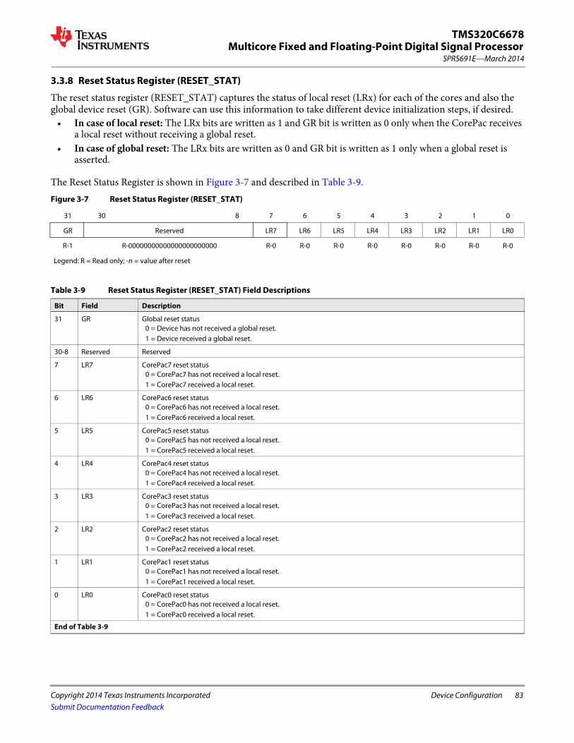
Multicore Fixed and Floating-Point Digital Signal Processor
Copyright 2014 Texas Instruments Incorporated Device Configuration 83
SPRS691E—March 2014
TMS320C6678
Submit Documentation Feedback
3.3.8 Reset Status Register (RESET_STAT)
The reset status register (RESET_STAT) captures the status of local reset (LRx) for each of the cores and also the global device reset (GR). Software can use this information to take different device initialization steps, if desired.
• In case of local reset: The LRx bits are written as 1 and GR bit is written as 0 only when the CorePac receives a local reset without receiving a global reset.
• In case of global reset: The LRx bits are written as 0 and GR bit is written as 1 only when a global reset is asserted.
The Reset Status Register is shown in Figure 3-7 and described in Table 3-9.Figure 3-7 Reset Status Register (RESET_STAT)
31 30 8 7 6 5 4 3 2 1 0
GR Reserved LR7 LR6 LR5 LR4 LR3 LR2 LR1 LR0
R-1 R-00000000000000000000000 R-0 R-0 R-0 R-0 R-0 R-0 R-0 R-0
Legend: R = Read only; -n = value after reset
Table 3-9 Reset Status Register (RESET_STAT) Field Descriptions
Bit Field Description
31 GR Global reset status0 = Device has not received a global reset.1 = Device received a global reset.
30-8 Reserved Reserved
7 LR7 CorePac7 reset status0 = CorePac7 has not received a local reset.1 = CorePac7 received a local reset.
6 LR6 CorePac6 reset status0 = CorePac6 has not received a local reset.1 = CorePac6 received a local reset.
5 LR5 CorePac5 reset status0 = CorePac5 has not received a local reset.1 = CorePac5 received a local reset.
4 LR4 CorePac4 reset status0 = CorePac4 has not received a local reset.1 = CorePac4 received a local reset.
3 LR3 CorePac3 reset status0 = CorePac3 has not received a local reset.1 = CorePac3 received a local reset.
2 LR2 CorePac2 reset status0 = CorePac2 has not received a local reset.1 = CorePac2 received a local reset.
1 LR1 CorePac1 reset status0 = CorePac1 has not received a local reset.1 = CorePac1 received a local reset.
0 LR0 CorePac0 reset status0 = CorePac0 has not received a local reset.1 = CorePac0 received a local reset.
End of Table 3-9

84 Device Configuration Copyright 2014 Texas Instruments Incorporated
SPRS691E—March 2014Multicore Fixed and Floating-Point Digital Signal ProcessorTMS320C6678
Submit Documentation Feedback
3.3.9 Reset Status Clear Register (RESET_STAT_CLR)
The RESET_STAT bits can be cleared by writing 1 to the corresponding bit in the RESET_STAT_CLR register. The Reset Status Clear Register is shown in Figure 3-8 and described in Table 3-10.Figure 3-8 Reset Status Clear Register (RESET_STAT_CLR)
31 30 8 7 6 5 4 3 2 1 0
GR Reserved LR7 LR6 LR5 LR4 LR3 LR2 LR1 LR0
RW-0 R - 000 0000 0000 0000 0000 0000 RW-0 RW-0 RW-0 RW-0 RW-0 RW-0 RW-0 RW-0
Legend: R = Read only; RW = Read/Write; -n = value after reset
Table 3-10 Reset Status Clear Register (RESET_STAT_CLR) Field Descriptions
Bit Field Description
31 GR Global reset clear bit0 = Writing a 0 has no effect.1 = Writing a 1 to the GR bit clears the corresponding bit in the RESET_STAT register.
30-8 Reserved Reserved.
7 LR7 CorePac7 reset clear bit0 = Writing a 0 has no effect.1 = Writing a 1 to the LR3 bit clears the corresponding bit in the RESET_STAT register.
6 LR6 CorePac6 reset clear bit0 = Writing a 0 has no effect.1 = Writing a 1 to the LR3 bit clears the corresponding bit in the RESET_STAT register.
5 LR5 CorePac5 reset clear bit0 = Writing a 0 has no effect.1 = Writing a 1 to the LR3 bit clears the corresponding bit in the RESET_STAT register.
4 LR4 CorePac4 reset clear bit0 = Writing a 0 has no effect.1 = Writing a 1 to the LR3 bit clears the corresponding bit in the RESET_STAT register.
3 LR3 CorePac3 reset clear bit0 = Writing a 0 has no effect.1 = Writing a 1 to the LR3 bit clears the corresponding bit in the RESET_STAT register.
2 LR2 CorePac2 reset clear bit0 = Writing a 0 has no effect.1 = Writing a 1 to the LR2 bit clears the corresponding bit in the RESET_STAT register.
1 LR1 CorePac1 reset clear bit0 = Writing a 0 has no effect.1 = Writing a 1 to the LR1 bit clears the corresponding bit in the RESET_STAT register.
0 LR0 CorePac0 reset clear bit0 = Writing a 0 has no effect.1 = Writing a 1 to the LR0 bit clears the corresponding bit in the RESET_STAT register.
End of Table 3-10
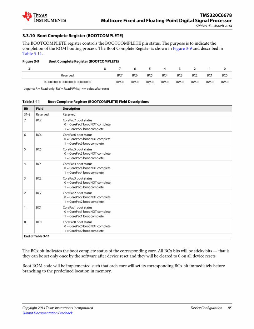
Multicore Fixed and Floating-Point Digital Signal Processor
Copyright 2014 Texas Instruments Incorporated Device Configuration 85
SPRS691E—March 2014
TMS320C6678
Submit Documentation Feedback
3.3.10 Boot Complete Register (BOOTCOMPLETE)
The BOOTCOMPLETE register controls the BOOTCOMPLETE pin status. The purpose is to indicate the completion of the ROM booting process. The Boot Complete Register is shown in Figure 3-9 and described in Table 3-11.
The BCx bit indicates the boot complete status of the corresponding core. All BCx bits will be sticky bits — that is they can be set only once by the software after device reset and they will be cleared to 0 on all device resets.
Boot ROM code will be implemented such that each core will set its corresponding BCx bit immediately before branching to the predefined location in memory.
Figure 3-9 Boot Complete Register (BOOTCOMPLETE)
31 8 7 6 5 4 3 2 1 0
Reserved BC7 BC6 BC5 BC4 BC3 BC2 BC1 BC0
R-0000 0000 0000 0000 0000 0000 RW-0 RW-0 RW-0 RW-0 RW-0 RW-0 RW-0 RW-0
Legend: R = Read only; RW = Read/Write; -n = value after reset
Table 3-11 Boot Complete Register (BOOTCOMPLETE) Field Descriptions
Bit Field Description
31-8 Reserved Reserved.
7 BC7 CorePac7 boot status0 = CorePac7 boot NOT complete1 = CorePac7 boot complete
6 BC6 CorePac6 boot status0 = CorePac6 boot NOT complete1 = CorePac6 boot complete
5 BC5 CorePac5 boot status0 = CorePac5 boot NOT complete1 = CorePac5 boot complete
4 BC4 CorePac4 boot status0 = CorePac4 boot NOT complete1 = CorePac4 boot complete
3 BC3 CorePac3 boot status0 = CorePac3 boot NOT complete1 = CorePac3 boot complete
2 BC2 CorePac2 boot status0 = CorePac2 boot NOT complete1 = CorePac2 boot complete
1 BC1 CorePac1 boot status0 = CorePac1 boot NOT complete1 = CorePac1 boot complete
0 BC0 CorePac0 boot status0 = CorePac0 boot NOT complete1 = CorePac0 boot complete
End of Table 3-11
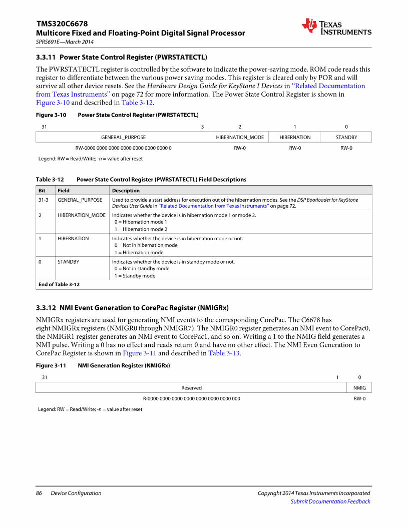
86 Device Configuration Copyright 2014 Texas Instruments Incorporated
SPRS691E—March 2014Multicore Fixed and Floating-Point Digital Signal ProcessorTMS320C6678
Submit Documentation Feedback
3.3.11 Power State Control Register (PWRSTATECTL)
The PWRSTATECTL register is controlled by the software to indicate the power-saving mode. ROM code reads this register to differentiate between the various power saving modes. This register is cleared only by POR and will survive all other device resets. See the Hardware Design Guide for KeyStone I Devices in ‘‘Related Documentation from Texas Instruments’’ on page 72 for more information. The Power State Control Register is shown in Figure 3-10 and described in Table 3-12.
3.3.12 NMI Event Generation to CorePac Register (NMIGRx)
NMIGRx registers are used for generating NMI events to the corresponding CorePac. The C6678 has eight NMIGRx registers (NMIGR0 through NMIGR7). The NMIGR0 register generates an NMI event to CorePac0, the NMIGR1 register generates an NMI event to CorePac1, and so on. Writing a 1 to the NMIG field generates a NMI pulse. Writing a 0 has no effect and reads return 0 and have no other effect. The NMI Even Generation to CorePac Register is shown in Figure 3-11 and described in Table 3-13.
Figure 3-10 Power State Control Register (PWRSTATECTL)
31 3 2 1 0
GENERAL_PURPOSE HIBERNATION_MODE HIBERNATION STANDBY
RW-0000 0000 0000 0000 0000 0000 0000 0 RW-0 RW-0 RW-0
Legend: RW = Read/Write; -n = value after reset
Table 3-12 Power State Control Register (PWRSTATECTL) Field Descriptions
Bit Field Description
31-3 GENERAL_PURPOSE Used to provide a start address for execution out of the hibernation modes. See the DSP Bootloader for KeyStone Devices User Guide in ‘‘Related Documentation from Texas Instruments’’ on page 72.
2 HIBERNATION_MODE Indicates whether the device is in hibernation mode 1 or mode 2.0 = Hibernation mode 11 = Hibernation mode 2
1 HIBERNATION Indicates whether the device is in hibernation mode or not.0 = Not in hibernation mode1 = Hibernation mode
0 STANDBY Indicates whether the device is in standby mode or not.0 = Not in standby mode1 = Standby mode
End of Table 3-12
Figure 3-11 NMI Generation Register (NMIGRx)
31 1 0
Reserved NMIG
R-0000 0000 0000 0000 0000 0000 0000 000 RW-0
Legend: RW = Read/Write; -n = value after reset

Multicore Fixed and Floating-Point Digital Signal Processor
Copyright 2014 Texas Instruments Incorporated Device Configuration 87
SPRS691E—March 2014
TMS320C6678
Submit Documentation Feedback
3.3.13 IPC Generation Registers (IPCGRx)
IPCGRx are the IPC interrupt generation registers to facilitate inter CorePac interrupts.
The C6678 has eight IPCGRx registers (IPCGR0 through IPCGR7). These registers can be used by external hosts or CorePacs to generate interrupts to other CorePacs. A write of 1 to IPCG field of IPCGRx register will generate an interrupt pulse to CorePacx (0 <= x <= 7).
These registers also provide a Source ID facility by which up to 28 different sources of interrupts can be identified. Allocation of source bits to source processor and meaning is entirely based on software convention. The register field descriptions are given in the following tables. Virtually anything can be a source for these registers as this is completely controlled by software. Any master that has access to BOOTCFG module space can write to these registers. The IPC Generation Register is shown in Figure 3-12 and described in Table 3-14.
Table 3-13 NMI Generation Register (NMIGRx) Field Descriptions
Bit Field Description
31-1 Reserved Reserved
0 NMIG NMI pulse generation.
Reads return 0
Writes:0 = No effect1 = Creates NMI pulse to the corresponding CorePac — CorePac0 for NMIGR0, etc.
End of Table 3-13
Figure 3-12 IPC Generation (IPCGRx) Registers
31 30 29 28 27 8 7 6 5 4 3 1 0
SRCS27 SRCS26 SRCS25 SRCS24 SRCS23 – SRCS4 SRCS3 SRCS2 SRCS1 SRCS0 Reserved IPCG
RW-0 RW-0 RW-0 RW-0 RW-0 (per bit field) RW-0 RW-0 RW-0 RW-0 R-000 RW-0
Legend: R = Read only; RW = Read/Write; -n = value after reset
Table 3-14 IPC Generation Registers (IPCGRx) Field Descriptions
Bit Field Description
31-4 SRCSx Interrupt source indication.
Reads return current value of internal register bit.
Writes:0 = No effect1 = Sets both SRCSx and the corresponding SRCCx.
3-1 Reserved Reserved
0 IPCG Inter-DSP interrupt generation.
Reads return 0.
Writes:0 = No effect1 = Creates an Inter-DSP interrupt.
End of Table 3-14

88 Device Configuration Copyright 2014 Texas Instruments Incorporated
SPRS691E—March 2014Multicore Fixed and Floating-Point Digital Signal ProcessorTMS320C6678
Submit Documentation Feedback
3.3.14 IPC Acknowledgement Registers (IPCARx)
IPCARx are the IPC interrupt-acknowledgement registers to facilitate inter-CorePac core interrupts.
The C6678 has eight IPCARx registers (IPCAR0 through IPCAR7). These registers also provide a Source ID facility by which up to 28 different sources of interrupts can be identified. Allocation of source bits to source processor and meaning is entirely based on software convention. The register field descriptions are shown in the following tables. Virtually anything can be a source for these registers as this is completely controlled by software. Any master that has access to BOOTCFG module space can write to these registers. The IPC Acknowledgement Register is shown in Figure 3-13 and described in Table 3-15.
3.3.15 IPC Generation Host Register (IPCGRH)
The IPCGRH register facilitates interrupts to external hosts. Operation and use of the IPCGRH register is the same as for other IPCGR registers. The interrupt output pulse created by the IPCGRH register appears on device pin HOUT.
The host interrupt output pulse is stretched so that it is asserted for four bootcfg clock (CPU/6) cycles followed by a deassertion of four bootcfg clock cycles. Generating the pulse results in a pulse-blocking window that is eight CPU/6-cycles long. Back to back writes to the IPCRGH register with the IPCG bit (bit 0) set, generates only one pulse if the back-to-back writes to IPCGRH are less than the eight CPU/6 cycle window -- the pulse blocking window. In order to generate back-to-back pulses, the back-to-back writes to the IPCGRH register must be greater than eight CPU/6 cycle window. The IPC Generation Host Register is shown in Figure 3-14 and described in Table 3-16.
Figure 3-13 IPC Acknowledgement (IPCARx) Registers
31 30 29 28 27 8 7 6 5 4 3 0
SRCC27 SRCC26 SRCC25 SRCC24 SRCC23 – SRCC4 SRCC3 SRCC2 SRCC1 SRCC0 Reserved
RW-0 RW-0 RW-0 RW-0 RW-0 (per bit field) RW-0 RW-0 RW-0 RW-0 R-0000
Legend: R = Read only; RW = Read/Write; -n = value after reset
Table 3-15 IPC Acknowledgement Registers (IPCARx) Field Descriptions
Bit Field Description
31-4 SRCCx Interrupt source acknowledgement.
Reads return current value of internal register bit.
Writes:0 = No effect1 = Clears both SRCCx and the corresponding SRCSx
3-0 Reserved Reserved
End of Table 3-15
Figure 3-14 IPC Generation (IPCGRH) Registers
31 30 29 28 27 8 7 6 5 4 3 1 0
SRCS27 SRCS26 SRCS25 SRCS24 SRCS23 – SRCS4 SRCS3 SRCS2 SRCS1 SRCS0 Reserved IPCG
RW-0 RW-0 RW-0 RW-0 RW-0 (per bit field) RW-0 RW-0 RW-0 RW-0 R-000 RW-0
Legend: R = Read only; RW = Read/Write; -n = value after reset

Multicore Fixed and Floating-Point Digital Signal Processor
Copyright 2014 Texas Instruments Incorporated Device Configuration 89
SPRS691E—March 2014
TMS320C6678
Submit Documentation Feedback
3.3.16 IPC Acknowledgement Host Register (IPCARH)
IPCARH registers are provided to facilitate host DSP interrupt. Operation and use of IPCARH is the same as other IPCAR registers. The IPC Acknowledgement Host Register is shown in Figure 3-15 and described in Table 3-17.
Table 3-16 IPC Generation Registers (IPCGRH) Field Descriptions
Bit Field Description
31-4 SRCSx Interrupt source indication.
Reads return current value of internal register bit.
Writes:0 = No effect1 = Sets both SRCSx and the corresponding SRCCx.
3-1 Reserved Reserved
0 IPCG Host interrupt generation.
Reads return 0.
Writes:0 = No effect1 = Creates an interrupt pulse on device pin (host interrupt/event output in HOUT pin)
End of Table 3-16
Figure 3-15 IPC Acknowledgement Register (IPCARH)
31 30 29 28 27 8 7 6 5 4 3 0
SRCC27 SRCC26 SRCC25 SRCC24 SRCC23 – SRCC4 SRCC3 SRCC2 SRCC1 SRCC0 Reserved
RW-0 RW-0 RW-0 RW-0 RW-0 (per bit field) RW-0 RW-0 RW-0 RW-0 R-0000
Legend: R = Read only; RW = Read/Write; -n = value after reset
Table 3-17 IPC Acknowledgement Register (IPCARH) Field Descriptions
Bit Field Description
31-4 SRCCx Interrupt source acknowledgement.
Reads return current value of internal register bit.
Writes:0 = No effect1 = Clears both SRCCx and the corresponding SRCSx
3-0 Reserved Reserved
End of Table 3-17

90 Device Configuration Copyright 2014 Texas Instruments Incorporated
SPRS691E—March 2014Multicore Fixed and Floating-Point Digital Signal ProcessorTMS320C6678
Submit Documentation Feedback
3.3.17 Timer Input Selection Register (TINPSEL)
Timer input selection is handled within the control register TINPSEL. The Timer Input Selection Register is shown in Figure 3-16 and described in Table 3-18Figure 3-16 Timer Input Selection Register (TINPSEL)
31 30 29 28 27 26 25 24 23 22 21 20 19 18 17 16
TINPHSEL15
TINPLSEL15
TINPHSEL14
TINPLSEL14
TINPHSEL13
TINPLSEL13
TINPHSEL12
TINPLSEL12
TINPHSEL11
TINPLSEL11
TINPHSEL10
TINPLSEL10
TINPHSEL9
TINPLSEL9
TINPHSEL8
TINPLSEL8
RW-1 RW-0 RW-1 RW-0 RW-1 RW-0 RW-1 RW-0 RW-1 RW-0 RW-1 RW-0 RW-1 RW-1 RW-1 RW-0spacer
15 14 13 12 11 10 9 8 7 6 5 4 3 2 1 0
TINPHSEL7
TINPLSEL7
TINPHSEL6
TINPLSEL6
TINPHSEL5
TINPLSEL5
TINPHSEL4
TINPLSEL4
TINPHSEL3
TINPLSEL3
TINPHSEL2
TINPLSEL2
TINPHSEL1
TINPLSEL1
TINPHSEL0
TINPLSEL0
RW-1 RW-0 RW-1 RW-0 RW-1 RW-0 RW-1 RW-0 RW-1 RW-0 RW-1 RW-0 RW-1 RW-1 RW-1 RW-0
Legend: R = Read only; RW = Read/Write; -n = value after reset
Table 3-18 Timer Input Selection Field Description (TINPSEL) (Sheet 1 of 3)
Bit Field Description
31 TINPHSEL15 Input select for TIMER15 high.0 = TIMI01 = TIMI1
30 TINPLSEL15 Input select for TIMER15 low.0 = TIMI01 = TIMI1
29 TINPHSEL14 Input select for TIMER14 high.0 = TIMI01 = TIMI1
28 TINPLSEL14 Input select for TIMER14 low.0 = TIMI01 = TIMI1
27 TINPHSEL13 Input select for TIMER13 high.0 = TIMI01 = TIMI1
26 TINPLSEL13 Input select for TIMER13 low.0 = TIMI01 = TIMI1
25 TINPHSEL12 Input select for TIMER12 high.0 = TIMI01 = TIMI1
24 TINPLSEL12 Input select for TIMER12 low.0 = TIMI01 = TIMI1
23 TINPHSEL11 Input select for TIMER11 high.0 = TIMI01 = TIMI1
22 TINPLSEL11 Input select for TIMER11 low.0 = TIMI01 = TIMI1
21 TINPHSEL10 Input select for TIMER10 high.0 = TIMI01 = TIMI1

Multicore Fixed and Floating-Point Digital Signal Processor
Copyright 2014 Texas Instruments Incorporated Device Configuration 91
SPRS691E—March 2014
TMS320C6678
Submit Documentation Feedback
20 TINPLSEL10 Input select for TIMER10 low.0 = TIMI01 = TIMI1
19 TINPHSEL9 Input select for TIMER9 high.0 = TIMI01 = TIMI1
18 TINPLSEL9 Input select for TIMER9 low.0 = TIMI01 = TIMI1
17 TINPHSEL8 Input select for TIMER8 high.0 = TIMI01 = TIMI1
16 TINPLSEL8 Input select for TIMER8 low.0 = TIMI01 = TIMI1
15 TINPHSEL7 Input select for TIMER7 high.0 = TIMI01 = TIMI1
14 TINPLSEL7 Input select for TIMER7 low.0 = TIMI01 = TIMI1
13 TINPHSEL6 Input select for TIMER6 high.0 = TIMI01 = TIMI1
12 TINPLSEL6 Input select for TIMER6 low.0 = TIMI01 = TIMI1
11 TINPHSEL5 Input select for TIMER5 high.0 = TIMI01 = TIMI1
10 TINPLSEL5 Input select for TIMER5 low.0 = TIMI01 = TIMI1
9 TINPHSEL4 Input select for TIMER4 high.0 = TIMI01 = TIMI1
8 TINPLSEL4 Input select for TIMER4 low.0 = TIMI01 = TIMI1
7 TINPHSEL3 Input select for TIMER3 high.0 = TIMI01 = TIMI1
6 TINPLSEL3 Input select for TIMER3 low.0 = TIMI01 = TIMI1
5 TINPHSEL2 Input select for TIMER2 high.0 = TIMI01 = TIMI1
4 TINPLSEL2 Input select for TIMER2 low.0 = TIMI01 = TIMI1
Table 3-18 Timer Input Selection Field Description (TINPSEL) (Sheet 2 of 3)
Bit Field Description

92 Device Configuration Copyright 2014 Texas Instruments Incorporated
SPRS691E—March 2014Multicore Fixed and Floating-Point Digital Signal ProcessorTMS320C6678
Submit Documentation Feedback
3 TINPHSEL1 Input select for TIMER1 high.0 = TIMI01 = TIMI1
2 TINPLSEL1 Input select for TIMER1 low.0 = TIMI01 = TIMI1
1 TINPHSEL0 Input select for TIMER0 high.0 = TIMI01 = TIMI1
0 TINPLSEL0 Input select for TIMER0 low.0 = TIMI01 = TIMI1
End of Table 3-18
Table 3-18 Timer Input Selection Field Description (TINPSEL) (Sheet 3 of 3)
Bit Field Description
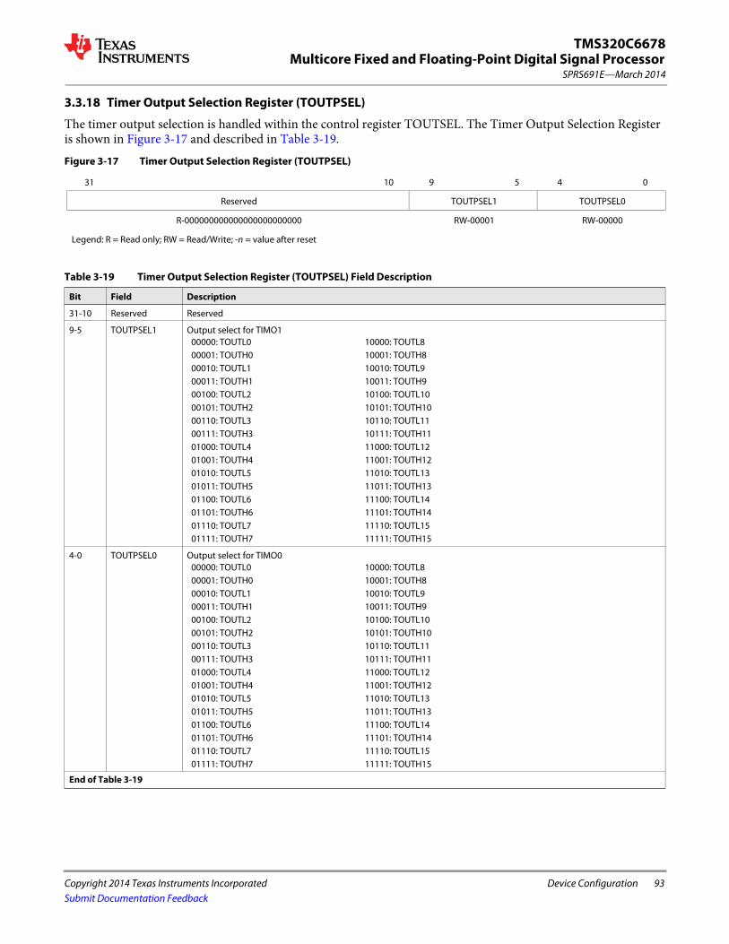
Multicore Fixed and Floating-Point Digital Signal Processor
Copyright 2014 Texas Instruments Incorporated Device Configuration 93
SPRS691E—March 2014
TMS320C6678
Submit Documentation Feedback
3.3.18 Timer Output Selection Register (TOUTPSEL)
The timer output selection is handled within the control register TOUTSEL. The Timer Output Selection Register is shown in Figure 3-17 and described in Table 3-19.Figure 3-17 Timer Output Selection Register (TOUTPSEL)
31 10 9 5 4 0
Reserved TOUTPSEL1 TOUTPSEL0
R-000000000000000000000000 RW-00001 RW-00000
Legend: R = Read only; RW = Read/Write; -n = value after reset
Table 3-19 Timer Output Selection Register (TOUTPSEL) Field Description
Bit Field Description
31-10 Reserved Reserved
9-5 TOUTPSEL1 Output select for TIMO100000: TOUTL0 00001: TOUTH000010: TOUTL100011: TOUTH100100: TOUTL200101: TOUTH200110: TOUTL300111: TOUTH301000: TOUTL401001: TOUTH401010: TOUTL501011: TOUTH501100: TOUTL601101: TOUTH601110: TOUTL701111: TOUTH7
10000: TOUTL8 10001: TOUTH810010: TOUTL910011: TOUTH910100: TOUTL1010101: TOUTH1010110: TOUTL1110111: TOUTH1111000: TOUTL1211001: TOUTH1211010: TOUTL1311011: TOUTH1311100: TOUTL1411101: TOUTH1411110: TOUTL1511111: TOUTH15
4-0 TOUTPSEL0 Output select for TIMO000000: TOUTL0 00001: TOUTH000010: TOUTL100011: TOUTH100100: TOUTL200101: TOUTH200110: TOUTL300111: TOUTH301000: TOUTL401001: TOUTH401010: TOUTL501011: TOUTH501100: TOUTL601101: TOUTH601110: TOUTL701111: TOUTH7
10000: TOUTL8 10001: TOUTH810010: TOUTL910011: TOUTH910100: TOUTL1010101: TOUTH1010110: TOUTL1110111: TOUTH1111000: TOUTL1211001: TOUTH1211010: TOUTL1311011: TOUTH1311100: TOUTL1411101: TOUTH1411110: TOUTL1511111: TOUTH15
End of Table 3-19
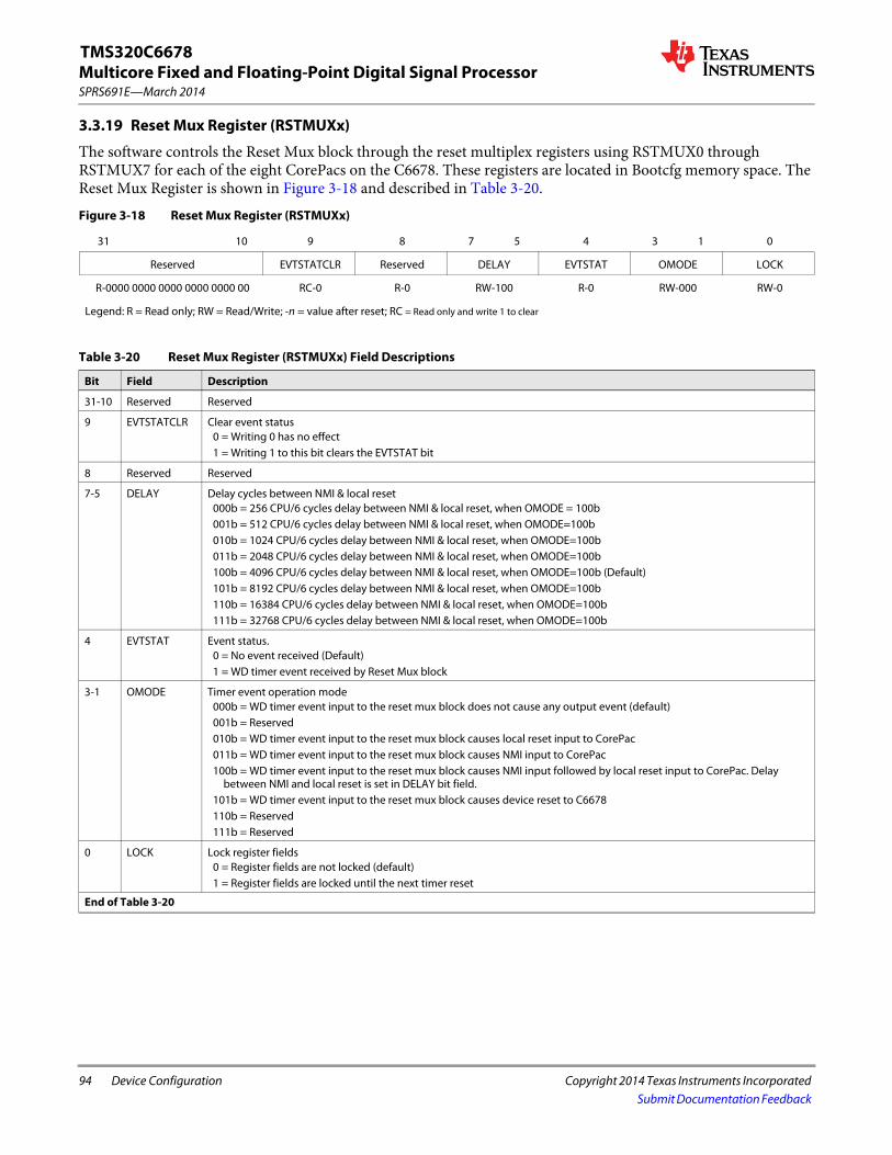
94 Device Configuration Copyright 2014 Texas Instruments Incorporated
SPRS691E—March 2014Multicore Fixed and Floating-Point Digital Signal ProcessorTMS320C6678
Submit Documentation Feedback
3.3.19 Reset Mux Register (RSTMUXx)
The software controls the Reset Mux block through the reset multiplex registers using RSTMUX0 through RSTMUX7 for each of the eight CorePacs on the C6678. These registers are located in Bootcfg memory space. The Reset Mux Register is shown in Figure 3-18 and described in Table 3-20.Figure 3-18 Reset Mux Register (RSTMUXx)
31 10 9 8 7 5 4 3 1 0
Reserved EVTSTATCLR Reserved DELAY EVTSTAT OMODE LOCK
R-0000 0000 0000 0000 0000 00 RC-0 R-0 RW-100 R-0 RW-000 RW-0
Legend: R = Read only; RW = Read/Write; -n = value after reset; RC = Read only and write 1 to clear
Table 3-20 Reset Mux Register (RSTMUXx) Field Descriptions
Bit Field Description
31-10 Reserved Reserved
9 EVTSTATCLR Clear event status0 = Writing 0 has no effect1 = Writing 1 to this bit clears the EVTSTAT bit
8 Reserved Reserved
7-5 DELAY Delay cycles between NMI & local reset000b = 256 CPU/6 cycles delay between NMI & local reset, when OMODE = 100b001b = 512 CPU/6 cycles delay between NMI & local reset, when OMODE=100b010b = 1024 CPU/6 cycles delay between NMI & local reset, when OMODE=100b011b = 2048 CPU/6 cycles delay between NMI & local reset, when OMODE=100b100b = 4096 CPU/6 cycles delay between NMI & local reset, when OMODE=100b (Default)101b = 8192 CPU/6 cycles delay between NMI & local reset, when OMODE=100b110b = 16384 CPU/6 cycles delay between NMI & local reset, when OMODE=100b111b = 32768 CPU/6 cycles delay between NMI & local reset, when OMODE=100b
4 EVTSTAT Event status.0 = No event received (Default)1 = WD timer event received by Reset Mux block
3-1 OMODE Timer event operation mode000b = WD timer event input to the reset mux block does not cause any output event (default)001b = Reserved010b = WD timer event input to the reset mux block causes local reset input to CorePac011b = WD timer event input to the reset mux block causes NMI input to CorePac100b = WD timer event input to the reset mux block causes NMI input followed by local reset input to CorePac. Delay
between NMI and local reset is set in DELAY bit field.101b = WD timer event input to the reset mux block causes device reset to C6678110b = Reserved111b = Reserved
0 LOCK Lock register fields0 = Register fields are not locked (default)1 = Register fields are locked until the next timer reset
End of Table 3-20
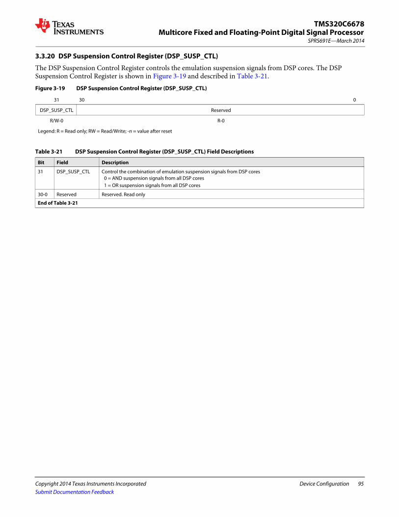
Multicore Fixed and Floating-Point Digital Signal Processor
Copyright 2014 Texas Instruments Incorporated Device Configuration 95
SPRS691E—March 2014
TMS320C6678
Submit Documentation Feedback
3.3.20 DSP Suspension Control Register (DSP_SUSP_CTL)
The DSP Suspension Control Register controls the emulation suspension signals from DSP cores. The DSP Suspension Control Register is shown in Figure 3-19 and described in Table 3-21.Figure 3-19 DSP Suspension Control Register (DSP_SUSP_CTL)
31 30 0
DSP_SUSP_CTL Reserved
R/W-0 R-0
Legend: R = Read only; RW = Read/Write; -n = value after reset
Table 3-21 DSP Suspension Control Register (DSP_SUSP_CTL) Field Descriptions
Bit Field Description
31 DSP_SUSP_CTL Control the combination of emulation suspension signals from DSP cores 0 = AND suspension signals from all DSP cores1 = OR suspension signals from all DSP cores
30-0 Reserved Reserved. Read only
End of Table 3-21
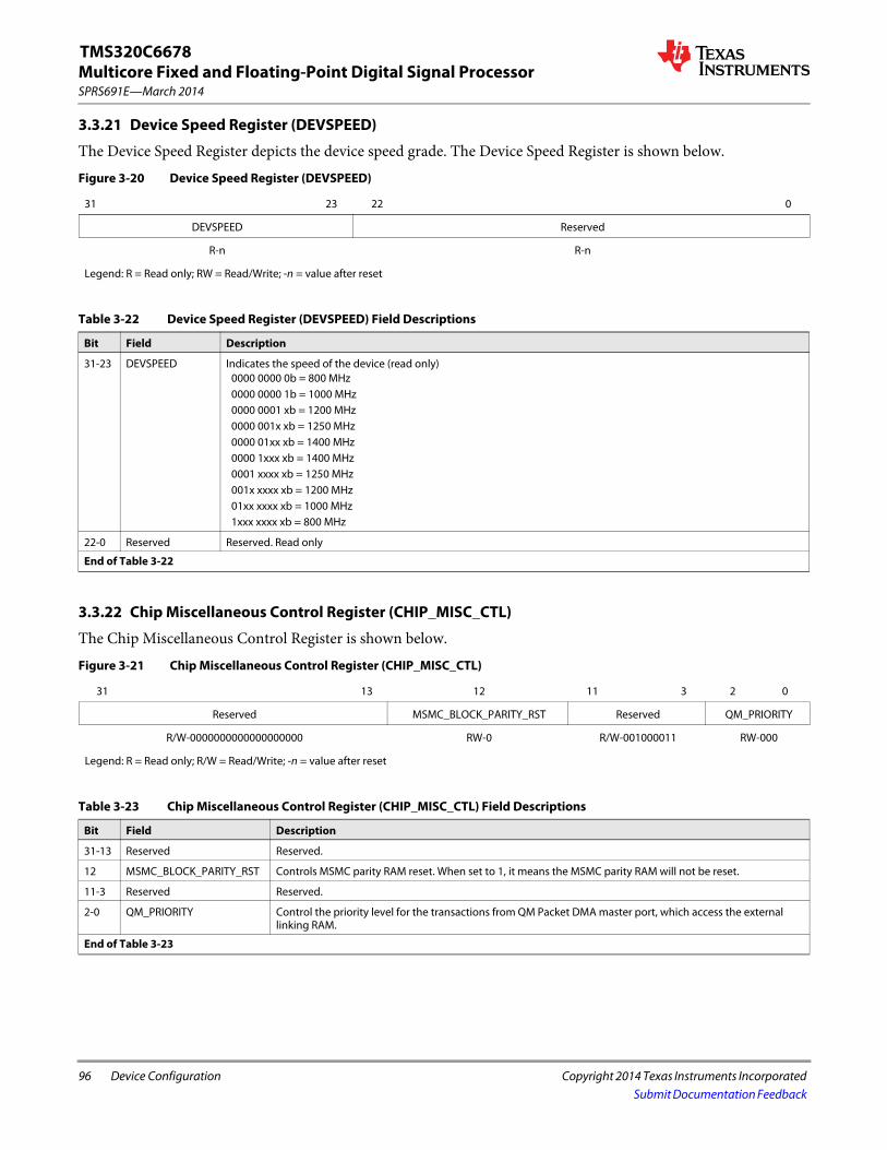
96 Device Configuration Copyright 2014 Texas Instruments Incorporated
SPRS691E—March 2014Multicore Fixed and Floating-Point Digital Signal ProcessorTMS320C6678
Submit Documentation Feedback
3.3.21 Device Speed Register (DEVSPEED)
The Device Speed Register depicts the device speed grade. The Device Speed Register is shown below.
3.3.22 Chip Miscellaneous Control Register (CHIP_MISC_CTL)
The Chip Miscellaneous Control Register is shown below.
Figure 3-20 Device Speed Register (DEVSPEED)
31 23 22 0
DEVSPEED Reserved
R-n R-n
Legend: R = Read only; RW = Read/Write; -n = value after reset
Table 3-22 Device Speed Register (DEVSPEED) Field Descriptions
Bit Field Description
31-23 DEVSPEED Indicates the speed of the device (read only)0000 0000 0b = 800 MHz0000 0000 1b = 1000 MHz 0000 0001 xb = 1200 MHz0000 001x xb = 1250 MHz0000 01xx xb = 1400 MHz0000 1xxx xb = 1400 MHz0001 xxxx xb = 1250 MHz001x xxxx xb = 1200 MHz01xx xxxx xb = 1000 MHz1xxx xxxx xb = 800 MHz
22-0 Reserved Reserved. Read only
End of Table 3-22
Figure 3-21 Chip Miscellaneous Control Register (CHIP_MISC_CTL)
31 13 12 11 3 2 0
Reserved MSMC_BLOCK_PARITY_RST Reserved QM_PRIORITY
R/W-0000000000000000000 RW-0 R/W-001000011 RW-000
Legend: R = Read only; R/W = Read/Write; -n = value after reset
Table 3-23 Chip Miscellaneous Control Register (CHIP_MISC_CTL) Field Descriptions
Bit Field Description
31-13 Reserved Reserved.
12 MSMC_BLOCK_PARITY_RST Controls MSMC parity RAM reset. When set to 1, it means the MSMC parity RAM will not be reset.
11-3 Reserved Reserved.
2-0 QM_PRIORITY Control the priority level for the transactions from QM Packet DMA master port, which access the external linking RAM.
End of Table 3-23

Multicore Fixed and Floating-Point Digital Signal Processor
Copyright 2014 Texas Instruments Incorporated Device Configuration 97
SPRS691E—March 2014
TMS320C6678
Submit Documentation Feedback
3.4 Pullup/Pulldown ResistorsProper board design should ensure that input pins to the device always be at a valid logic level and not floating. This may be achieved via pullup/pulldown resistors. The device features internal pullup (IPU) and internal pulldown (IPD) resistors on most pins to eliminate the need, unless otherwise noted, for external pullup/pulldown resistors.
An external pullup/pulldown resistor must be used in the following situations: • Device Configuration Pins: If the pin is both routed out and are not driven (in Hi-Z state), an external
pullup/pulldown resistor must be used, even if the IPU/IPD matches the desired value/state. • Other Input Pins: If the IPU/IPD does not match the desired value/state, use an external pullup/pulldown
resistor to pull the signal to the opposite rail.
For the device configuration pins (listed in Table 3-1), if they are both routed out and are not driven (in Hi-Z state), it is strongly recommended that an external pullup/pulldown resistor be implemented. Although, internal pullup/pulldown resistors exist on these pins and they may match the desired configuration value, providing external connectivity can help ensure that valid logic levels are latched on these device configuration pins. In addition, applying external pullup/pulldown resistors on the device configuration pins adds convenience to the user in debugging and flexibility in switching operating modes.
Tips for choosing an external pullup/pulldown resistor: • Consider the total amount of current that may pass through the pullup or pulldown resistor. Make sure to
include the leakage currents of all the devices connected to the net, as well as any internal pullup or pulldown resistors.
• Decide a target value for the net. For a pulldown resistor, this should be below the lowest VIL level of all inputs connected to the net. For a pullup resistor, this should be above the highest VIH level of all inputs on the net. A reasonable choice would be to target the VOL or VOH levels for the logic family of the limiting device; which, by definition, have margin to the VIL and VIH levels.
• Select a pullup/pulldown resistor with the largest possible value that can still ensure that the net will reach the target pulled value when maximum current from all devices on the net is flowing through the resistor. The current to be considered includes leakage current plus, any other internal and external pullup/pulldown resistors on the net.
• For bidirectional nets, there is an additional consideration that sets a lower limit on the resistance value of the external resistor. Verify that the resistance is small enough that the weakest output buffer can drive the net to the opposite logic level (including margin).
• Remember to include tolerances when selecting the resistor value. • For pullup resistors, also remember to include tolerances on the DVDD rail.
For most systems:• A 1-k resistor can be used to oppose the IPU/IPD while meeting the above criteria. Users should confirm this
resistor value is correct for their specific application. • A 20-k resistor can be used to compliment the IPU/IPD on the device configuration pins while meeting the
above criteria. Users should confirm this resistor value is correct for their specific application.
For more detailed information on input current (II), and the low-level/high-level input voltages (VIL and VIH) for the TMS320C6678 device, see Section 6.3 ‘‘Electrical Characteristics’’ on page 118.
To determine which pins on the device include internal pullup/pulldown resistors, see Table 2-26 ‘‘Terminal Functions — Signals and Control by Function’’ on page 44.

98 System Interconnect Copyright 2014 Texas Instruments Incorporated
SPRS691E—March 2014Multicore Fixed and Floating-Point Digital Signal ProcessorTMS320C6678
Submit Documentation Feedback
4 System InterconnectOn the TMS320C6678 device, the C66x CorePacs, the EDMA3 transfer controllers, and the system peripherals are interconnected through the TeraNet, which is a non-blocking switch fabric enabling fast and contention-free internal data movement. The TeraNet allows for low-latency, concurrent data transfers between master peripherals and slave peripherals. The TeraNet also allows for seamless arbitration between the system masters when accessing system slaves.
4.1 Internal Buses and Switch Fabrics Two types of buses exist in the device: data buses and configuration buses. Some peripherals have both a data bus and a configuration bus interface, while others have only one type of interface. Further, the bus interface width and speed varies from peripheral to peripheral. Configuration buses are mainly used to access the register space of a peripheral and the data buses are used mainly for data transfers.
The C66x CorePacs, the EDMA3 traffic controllers, and the various system peripherals can be classified into two categories: masters and slaves. Masters are capable of initiating read and write transfers in the system and do not rely on the EDMA3 for their data transfers. Slaves, on the other hand, rely on the masters to perform transfers to and from them. Examples of masters include the EDMA3 traffic controllers, SRIO, and Network Coprocessor packet DMA. Examples of slaves include the SPI, UART, and I2C.
The masters and slaves in the device are communicating through the TeraNet (switch fabric). The device contains two switch fabrics. The data switch fabric (data TeraNet) and the configuration switch fabric (configuration TeraNet). The data TeraNet, is a high-throughput interconnect mainly used to move data across the system. The data TeraNet connects masters to slaves via data buses. Some peripherals require a bridge to connect to the data TeraNet. The configuration TeraNet, is mainly used to access peripheral registers. The configuration TeraNet connects masters to slaves via configuration buses. As with the data TeraNet, some peripherals require the use of a bridge to interface to the configuration TeraNet. Note that the data TeraNet also connects to the configuration TeraNet. For more details see 4.2 ‘‘Switch Fabric Connections’’.
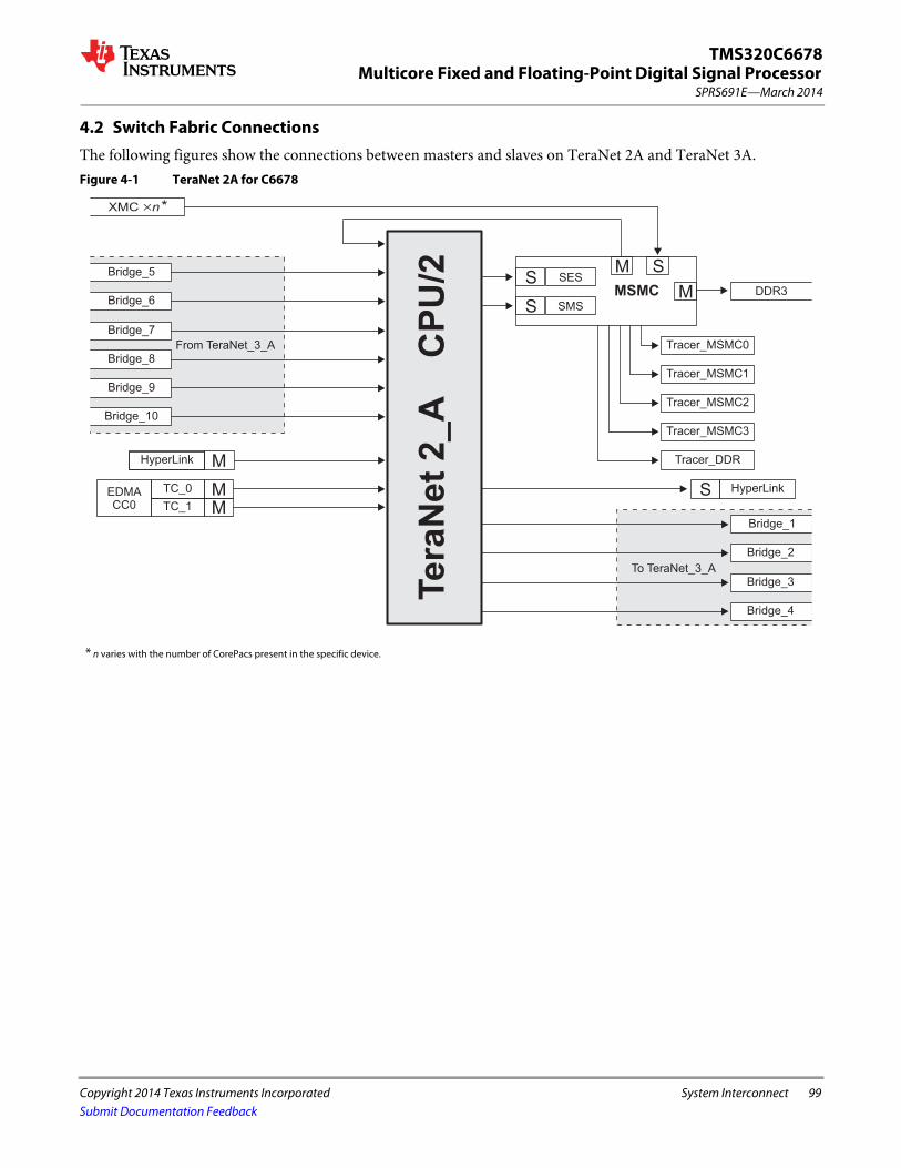
Multicore Fixed and Floating-Point Digital Signal Processor
Copyright 2014 Texas Instruments Incorporated System Interconnect 99
SPRS691E—March 2014
TMS320C6678
Submit Documentation Feedback
4.2 Switch Fabric ConnectionsThe following figures show the connections between masters and slaves on TeraNet 2A and TeraNet 3A. Figure 4-1 TeraNet 2A for C6678
* n varies with the number of CorePacs present in the specific device.
Te
raN
et
2_
AC
PU
/2
Bridge_1
Bridge_2
Bridge_3
Bridge_4
To TeraNet_3_A
Tracer_MSMC0
EDMACC0 TC_1 M
TC_0 M
HyperLink M
Bridge_5
Bridge_6
Bridge_7
Bridge_8From TeraNet_3_A
Bridge_9
Bridge_10
Tracer_MSMC1
Tracer_MSMC2
Tracer_MSMC3
Tracer_DDR
XMC �n*
SESS
SMSSMSMC M
M S
DDR3
HyperLinkS

100 System Interconnect Copyright 2014 Texas Instruments Incorporated
SPRS691E—March 2014Multicore Fixed and Floating-Point Digital Signal ProcessorTMS320C6678
Submit Documentation Feedback
Figure 4-2 TeraNet 3A for C6678
* n varies with the number of CorePacs present in the specific device.
Te
raN
et
3_
AC
PU
/3
TSIP0 M
TSIP1 M
Bridge_1
Bridge_2
Bridge_3
Bridge_4
From TeraNet_2_A
Bridge_5
Bridge_6
Bridge_7
Bridge_8
To TeraNet_2_A
Bridge_9
Bridge_10
Bridge_12
Bridge_13
Bridge_14
To TeraNet_3P_A
Boot_ROMS
SPISTNet_6P_A
CPU/3
PCIeS
SRIOS
QM_SSSTracer_QM_M
MPU_1
CorePac_ *nSTracer_L2_ *n
EMIF16S
TC_3 M
EDMACC1 TC_2 M
TC_1 M
TC_0 M
TC_3 M
EDMACC2 TC_2 M
TC_1 M
TC_0 M
SRIOPacket DMA M
QM_SSPacket DMA M
QM_SSSecond M
Debug_SS M
TNet_3_DCPU/3
PCIe M
SRIO_M M
NETCP M
TNet_3_CCPU/3

Multicore Fixed and Floating-Point Digital Signal Processor
Copyright 2014 Texas Instruments Incorporated System Interconnect 101
SPRS691E—March 2014
TMS320C6678
Submit Documentation Feedback
Allowed connections on TeraNet 2A and TeraNet 3A are summarized in the table below.
Intersecting cells may contain one of the following:• Y — There is a direct connection between this master and that slave.• - — There is NO connection between this master and that slave.• n — A numeric value indicates that the path between this master and that slave goes through bridge n.
Table 4-1 Switch Fabric Connection Matrix Section 1
Masters
SlavesH
yper
Link
_Sla
ve
MSM
C_SE
S
MSM
C_SM
S
Core
Pac0
_SD
MA
Core
Pac1
_SD
MA
Core
Pac2
_SD
MA
Core
Pac3
_SD
MA
Core
Pac4
_SD
MA
Core
Pac5
_SD
MA
Core
Pac6
_SD
MA
Core
Pac7
_SD
MA
SRIO
_Sla
ve
Boot
_RO
M
SPI
EMIF
16
PCIe
_Sla
ve
QM
_Sla
ve
HyperLink_Master - Y Y 1 1 1 1 1 1 1 1 1 1 1 1 1 1
EDMA3CC0_TC0_RD Y Y Y 2 2 2 2 2 2 2 2 2 2 2 2 2 -
EDMA3CC0_TC0_WR Y Y Y 2 2 2 2 2 2 2 2 2 - 2 2 2 -
EDMA3CC0_TC1_RD Y Y Y 3 3 3 3 3 3 3 3 3 3 3 3 3 -
EDMA3CC0_TC1_WR Y Y Y 3 3 3 3 3 3 3 3 3 - 3 3 3 -
EDMA3CC1_TC0_RD 5 5 5 Y Y Y Y Y Y Y Y Y Y Y Y Y -
EDMA3CC1_TC0_WR 5 5 5 Y Y Y Y Y Y Y Y Y - Y Y Y -
EDMA3CC1_TC1_RD 6 6 6 Y Y Y Y Y Y Y Y Y Y Y Y Y Y
EDMA3CC1_TC1_WR 6 6 6 Y Y Y Y Y Y Y Y Y - Y Y Y Y
EDMA3CC1_TC2_RD 7 7 7 Y Y Y Y Y Y Y Y Y Y Y Y Y -
EDMA3CC1_TC2_WR 7 7 7 Y Y Y Y Y Y Y Y Y - Y Y Y -
EDMA3CC1_TC3_RD 8 8 8 Y Y Y Y Y Y Y Y Y Y Y Y Y -
EDMA3CC1_TC3_WR 8 8 8 Y Y Y Y Y Y Y Y Y - Y Y Y -
EDMA3CC2_TC0_RD 9 9 9 Y Y Y Y Y Y Y Y Y Y Y Y Y -
EDMA3CC2_TC0_WR 9 9 9 Y Y Y Y Y Y Y Y Y - Y Y Y -
EDMA3CC2_TC1_RD 10 10 10 Y Y Y Y Y Y Y Y Y Y Y Y Y Y
EDMA3CC2_TC1_WR 10 10 10 Y Y Y Y Y Y Y Y Y - Y Y Y Y
EDMA3CC2_TC2_RD 5 5 5 Y Y Y Y Y Y Y Y Y Y Y Y Y -
EDMA3CC2_TC2_WR 5 5 5 Y Y Y Y Y Y Y Y Y - Y Y Y -
EDMA3CC2_TC3_RD 6 6 6 Y Y Y Y Y Y Y Y Y Y Y Y Y -
EDMA3CC2_TC3_WR 6 6 6 Y Y Y Y Y Y Y Y Y - Y Y Y -
SRIO packet DMA - 9 9 Y Y Y Y Y Y Y Y - - - Y - Y
SRIO_Master 9 9 9 Y Y Y Y Y Y Y Y - - Y Y - Y
PCIe_Master 7 7 7 Y Y Y Y Y Y Y Y - - Y Y - Y
NETCP packet DMA - 10 10 Y Y Y Y Y Y Y Y - - - - - Y
MSMC_Data_Master Y - - 4 4 4 4 4 4 4 4 4 4 4 4 4 4
QM Packet DMA 8 8 8 Y Y Y Y Y Y Y Y - - - - - Y
QM Second 8 8 8 Y Y Y Y Y Y Y Y - - - - - -
DebugSS_Master 10 10 10 Y Y Y Y Y Y Y Y Y Y Y Y Y Y
TSIP0_Master - 5 5 Y Y Y Y Y Y Y Y - - - - - -
TSIP1_Master - 5 5 Y Y Y Y Y Y Y Y - - - - - -
End of Table 4-1

102 System Interconnect Copyright 2014 Texas Instruments Incorporated
SPRS691E—March 2014Multicore Fixed and Floating-Point Digital Signal ProcessorTMS320C6678
Submit Documentation Feedback
The following figure shows the connection between masters and slaves on TeraNet 3P and TeraNet 6P. Figure 4-3 TeraNet 3P_A & B for C6678
* n varies with the number of CorePacs present in the specific device.
Te
raN
et
3P
_A
CP
U/3
To TeraNet_3P_Tracer
Bridge_12
Bridge_13
Bridge_14
From TeraNet_3_A
CorePac_ *n M
TETB (Debug_SS)
TETB (for core)
S
STNet_3P_D
CPU/3
S
STNet_3P_C
CPU/3
CC0S
TC ( 2)×STNet_2PCPU/2
SemaphoreSTracer_SM
MPU_3
QM_SSSTracer_QM_CFG
MPU_2
MPU ( 4)×S
Te
raN
et
3P
_B
CP
U/3
TSIP1S
NETCPS
TracerS
SRIOS
Bridge_20To TeraNet_6P_B
TSIP0S
Tracer_CFGMPU_0
CC1
TC ( 4)×
TC ( 4)×
CC2

Multicore Fixed and Floating-Point Digital Signal Processor
Copyright 2014 Texas Instruments Incorporated System Interconnect 103
SPRS691E—March 2014
TMS320C6678
Submit Documentation Feedback
Figure 4-4 TeraNet 6P_B and 3P_Tracer for C6678
* n varies with the number of CorePacs present in the specific device.
Te
raN
et
6P
_B
CP
U/6
Bridge_20
From TeraNet_3P_B GPIOS
SmartReflexS
TimerS
CICS
PLL_CTLS
PSCS
BOOTCFGS
UARTS
I C2S
Debug_SSS
Te
raN
et
3P
_T
rac
er
CP
U/3
Tracer_SM M
Tracer_DDR M
Tracer_L2_ *n
Tracer_QM_P M
Tracer_QM_M M
Tracer_CFG M
Tracer_MSMC_3 M
Tracer_MSMC_2 M
Tracer_MSMC_1 M
Tracer_MSMC_0 M
Debug_SSSTMS
Debug_SSTETBS
M
From TeraNet_3P_A
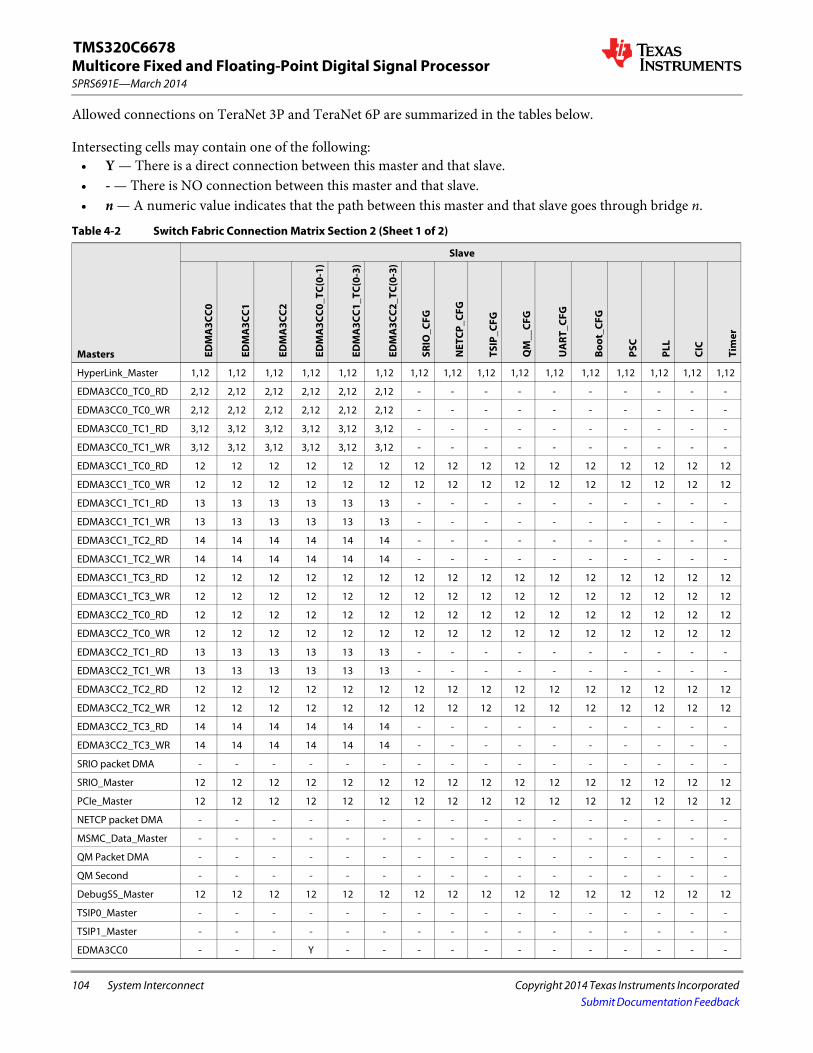
104 System Interconnect Copyright 2014 Texas Instruments Incorporated
SPRS691E—March 2014Multicore Fixed and Floating-Point Digital Signal ProcessorTMS320C6678
Submit Documentation Feedback
Allowed connections on TeraNet 3P and TeraNet 6P are summarized in the tables below.
Intersecting cells may contain one of the following:• Y — There is a direct connection between this master and that slave.• - — There is NO connection between this master and that slave.• n — A numeric value indicates that the path between this master and that slave goes through bridge n.
Table 4-2 Switch Fabric Connection Matrix Section 2 (Sheet 1 of 2)
Masters
Slave
EDM
A3C
C0
EDM
A3C
C1
EDM
A3C
C2
EDM
A3C
C0_T
C(0-
1)
EDM
A3C
C1_T
C(0-
3)
EDM
A3C
C2_T
C(0-
3)
SRIO
_CFG
NET
CP_C
FG
TSIP
_CFG
QM
__CF
G
UA
RT_C
FG
Boot
_CFG
PSC
PLL
CIC
Tim
er
HyperLink_Master 1,12 1,12 1,12 1,12 1,12 1,12 1,12 1,12 1,12 1,12 1,12 1,12 1,12 1,12 1,12 1,12
EDMA3CC0_TC0_RD 2,12 2,12 2,12 2,12 2,12 2,12 - - - - - - - - - -
EDMA3CC0_TC0_WR 2,12 2,12 2,12 2,12 2,12 2,12 - - - - - - - - - -
EDMA3CC0_TC1_RD 3,12 3,12 3,12 3,12 3,12 3,12 - - - - - - - - - -
EDMA3CC0_TC1_WR 3,12 3,12 3,12 3,12 3,12 3,12 - - - - - - - - - -
EDMA3CC1_TC0_RD 12 12 12 12 12 12 12 12 12 12 12 12 12 12 12 12
EDMA3CC1_TC0_WR 12 12 12 12 12 12 12 12 12 12 12 12 12 12 12 12
EDMA3CC1_TC1_RD 13 13 13 13 13 13 - - - - - - - - - -
EDMA3CC1_TC1_WR 13 13 13 13 13 13 - - - - - - - - - -
EDMA3CC1_TC2_RD 14 14 14 14 14 14 - - - - - - - - - -
EDMA3CC1_TC2_WR 14 14 14 14 14 14 - - - - - - - - - -
EDMA3CC1_TC3_RD 12 12 12 12 12 12 12 12 12 12 12 12 12 12 12 12
EDMA3CC1_TC3_WR 12 12 12 12 12 12 12 12 12 12 12 12 12 12 12 12
EDMA3CC2_TC0_RD 12 12 12 12 12 12 12 12 12 12 12 12 12 12 12 12
EDMA3CC2_TC0_WR 12 12 12 12 12 12 12 12 12 12 12 12 12 12 12 12
EDMA3CC2_TC1_RD 13 13 13 13 13 13 - - - - - - - - - -
EDMA3CC2_TC1_WR 13 13 13 13 13 13 - - - - - - - - - -
EDMA3CC2_TC2_RD 12 12 12 12 12 12 12 12 12 12 12 12 12 12 12 12
EDMA3CC2_TC2_WR 12 12 12 12 12 12 12 12 12 12 12 12 12 12 12 12
EDMA3CC2_TC3_RD 14 14 14 14 14 14 - - - - - - - - - -
EDMA3CC2_TC3_WR 14 14 14 14 14 14 - - - - - - - - - -
SRIO packet DMA - - - - - - - - - - - - - - - -
SRIO_Master 12 12 12 12 12 12 12 12 12 12 12 12 12 12 12 12
PCIe_Master 12 12 12 12 12 12 12 12 12 12 12 12 12 12 12 12
NETCP packet DMA - - - - - - - - - - - - - - - -
MSMC_Data_Master - - - - - - - - - - - - - - - -
QM Packet DMA - - - - - - - - - - - - - - - -
QM Second - - - - - - - - - - - - - - - -
DebugSS_Master 12 12 12 12 12 12 12 12 12 12 12 12 12 12 12 12
TSIP0_Master - - - - - - - - - - - - - - - -
TSIP1_Master - - - - - - - - - - - - - - - -
EDMA3CC0 - - - Y - - - - - - - - - - - -

Multicore Fixed and Floating-Point Digital Signal Processor
Copyright 2014 Texas Instruments Incorporated System Interconnect 105
SPRS691E—March 2014
TMS320C6678
Submit Documentation Feedback
EDMA3CC1 - - - - Y - - - - - - - - - - -
EDMA3CC2 - - - - - Y - - - - - - - - - -
CorePac0_CFG Y Y Y Y Y Y Y Y Y Y Y Y Y Y Y Y
CorePac1_CFG Y Y Y Y Y Y Y Y Y Y Y Y Y Y Y Y
CorePac2_CFG Y Y Y Y Y Y Y Y Y Y Y Y Y Y Y Y
CorePac3_CFG Y Y Y Y Y Y Y Y Y Y Y Y Y Y Y Y
CorePac4_CFG Y Y Y Y Y Y Y Y Y Y Y Y Y Y Y Y
CorePac5_CFG Y Y Y Y Y Y Y Y Y Y Y Y Y Y Y Y
CorePac6_CFG Y Y Y Y Y Y Y Y Y Y Y Y Y Y Y Y
CorePac7_CFG Y Y Y Y Y Y Y Y Y Y Y Y Y Y Y Y
End of Table 4-2
Table 4-3 Switch Fabric Connection Matrix Section 3 (Sheet 1 of 2)
Masters
Slave
GPI
O
I2 C
Sem
apho
re
Smar
tRef
lex
MPU
Trac
er
Deb
ug_S
S_CF
G
TETB
_Sys
tem
TETB
0
TETB
1
TETB
2
TETB
3
TETB
4
TETB
5
TETB
6
TETB
7
HyperLink_Master 1,12 1,12 1,12 1,12 1,12 1,12 1,12 - - - - - - - - -
EDMA3CC0_TC0_RD - - - - - - - 2,12 - - - - 2,12 2,12
EDMA3CC0_TC0_WR - - - - - - - - - - - - - - - -
EDMA3CC0_TC1_RD - - - - - - - 3,12 - - - - 3,12 3,12 - -
EDMA3CC0_TC1_WR - - - - - - - - - - - - - - - -
EDMA3CC1_TC0_RD 12 12 12 12 12 12 12 12 - - - - 12 12 - -
EDMA3CC1_TC0_WR 12 12 12 12 12 12 12 - - - - - - - - -
EDMA3CC1_TC1_RD - - - - - - - - 13 13 - - - - 13 -
EDMA3CC1_TC1_WR - - - - - - - - - - - - - - - -
EDMA3CC1_TC2_RD - - - - - - - - - - 14 14 - - - 14
EDMA3CC1_TC2_WR - - - - - - - - - - - - - - - -
EDMA3CC1_TC3_RD 12 12 12 12 12 12 12 12 - - - - 12 12 - -
EDMA3CC1_TC3_WR 12 12 12 12 12 12 12 - - - - - - - - -
EDMA3CC2_TC0_RD 12 12 12 12 12 12 12 12 - - - - 12 12 - -
EDMA3CC2_TC0_WR 12 12 12 12 12 12 12 - - - - - - - - -
EDMA3CC2_TC1_RD - - - - - - - - 13 13 - - - - 13 -
EDMA3CC2_TC1_WR - - - - - - - - - - - - - - - -
EDMA3CC2_TC2_RD 12 12 12 12 12 12 12 12 - - - - 12 12 - -
EDMA3CC2_TC2_WR 12 12 12 12 12 12 12 - - - - - - - - -
Table 4-2 Switch Fabric Connection Matrix Section 2 (Sheet 2 of 2)
Masters
Slave
EDM
A3C
C0
EDM
A3C
C1
EDM
A3C
C2
EDM
A3C
C0_T
C(0-
1)
EDM
A3C
C1_T
C(0-
3)
EDM
A3C
C2_T
C(0-
3)
SRIO
_CFG
NET
CP_C
FG
TSIP
_CFG
QM
__CF
G
UA
RT_C
FG
Boot
_CFG
PSC
PLL
CIC
Tim
er

106 System Interconnect Copyright 2014 Texas Instruments Incorporated
SPRS691E—March 2014Multicore Fixed and Floating-Point Digital Signal ProcessorTMS320C6678
Submit Documentation Feedback
EDMA3CC2_TC3_RD - - - - - - - - - - 14 14 - - - 14
EDMA3CC2_TC3_WR - - - - - - - - - - - - - - - -
SRIO packet DMA - - - - - - - - - - - - - - - -
SRIO_Master 12 12 12 12 12 12 12 12 12 12 12 12 12 12 12 12
PCIe_Master 12 12 12 12 12 12 12 12 12 12 12 12 12 12 12 12
NETCP packet DMA - - - - - - - - - - - - - - - -
MSMC_Data_Master - - - - - - - - - - - - - - - -
QM Packet DMA - - - - - - - - - - - - - - - -
QM Second - - - - - - - - - - - - - - - -
DebugSS_Master 12 12 12 12 12 12 12 12 12 12 12 12 12 12 12 12
TSIP0_Master - - - - - - - - - - - - - - - -
TSIP1_Master - - - - - - - - - - - - - - - -
EDMA3CC0 - - - - - - - - - - - - - - - -
EDMA3CC1 - - - - - - - - - - - - - - - -
EDMA3CC2 - - - - - - - - - - - - - - - -
CorePac0_CFG Y Y Y Y Y Y Y Y Y Y Y Y Y Y Y Y
CorePac1_CFG Y Y Y Y Y Y Y Y Y Y Y Y Y Y Y Y
CorePac2_CFG Y Y Y Y Y Y Y Y Y Y Y Y Y Y Y Y
CorePac3_CFG Y Y Y Y Y Y Y Y Y Y Y Y Y Y Y Y
CorePac4_CFG Y Y Y Y Y Y Y Y Y Y Y Y Y Y Y Y
CorePac5_CFG Y Y Y Y Y Y Y Y Y Y Y Y Y Y Y Y
CorePac6_CFG Y Y Y Y Y Y Y Y Y Y Y Y Y Y Y Y
CorePac7_CFG Y Y Y Y Y Y Y Y Y Y Y Y Y Y Y Y
End of Table 4-3
Table 4-3 Switch Fabric Connection Matrix Section 3 (Sheet 2 of 2)
Masters
Slave
GPI
O
I2 C
Sem
apho
re
Smar
tRef
lex
MPU
Trac
er
Deb
ug_S
S_CF
G
TETB
_Sys
tem
TETB
0
TETB
1
TETB
2
TETB
3
TETB
4
TETB
5
TETB
6
TETB
7

Multicore Fixed and Floating-Point Digital Signal Processor
Copyright 2014 Texas Instruments Incorporated System Interconnect 107
SPRS691E—March 2014
TMS320C6678
Submit Documentation Feedback
4.3 Bus PrioritiesThe priority level of all master peripheral traffic is defined at the TeraNet boundary. User programmable priority registers allow software configuration of the data traffic through the TeraNet. Note that a lower number means higher priority - PRI = 000b = urgent, PRI = 111b = low.
All other masters provide their priority directly and do not need a default priority setting. Examples include the CorePacs, whose priorities are set through software in the UMC control registers. All the packet-DMA-based peripherals also have internal registers to define the priority level of their initiated transactions.
The QM Packet DMA master port is one master port that does not have priority allocation register inside the IP. The priority level for transaction from this master port is described by QM_PRIORITY bit field in CHIP_MISC_CTL register in section 3.3.22 .
For all other modules, see the respective User Guides in “Related Documentation from Texas Instruments” on page 72 for programmable priority registers.

108 C66x CorePac Copyright 2014 Texas Instruments Incorporated
SPRS691E—March 2014Multicore Fixed and Floating-Point Digital Signal ProcessorTMS320C6678
Submit Documentation Feedback
5 C66x CorePac The C66x CorePac consists of several components:
• The C66x DSP and associated C66x CorePac core• Level-one and level-two memories (L1P, L1D, L2) • Data Trace Formatter (DTF)• Embedded Trace Buffer (ETB)• Interrupt Controller• Power-down controller• External Memory Controller• Extended Memory Controller• A dedicated power/sleep controller (LPSC)
The C66x CorePac also provides support for memory protection, bandwidth management (for resources local to the C66x CorePac) and address extension. Figure 5-1 shows a block diagram of the C66x CorePac.Figure 5-1 C66x CorePac Block Diagram
For more detailed information on the TMS320C66x CorePac on the C6678 device, see the C66x DSP CorePac User Guide in ‘‘Related Documentation from Texas Instruments’’ on page 72.
BootController
LPSCPLLC
GPSC
.L1 .S1.M1xxxx
.D1 .D2.M2xxxx
.S2 .L2
Data Memory Controller (DMC) WithMemory Protect/Bandwidth Mgmt
32KB L1D
CFG SwitchFabric
Data Path A
A Register File
A31-A16
A15-A0
Data Path B
B Register File
B31-B16
B15-B0
C66x DSP Core
Instruction Fetch
16-/32-bit Instruction Dispatch
Control Registers
In-Circuit Emulation
Instruction Decode
32KB L1P
Program Memory Controller (PMC) WithMemory Protect/Bandwidth Mgmt
L2 Cache/SRAM512KB
Inte
rru
pt
an
dE
xc
ep
tio
nC
on
tro
lle
r Un
ifie
dM
em
ory
Co
ntr
oll
er
(UM
C)
Ex
tern
al
Me
mo
ryC
on
tro
lle
r(E
MC
)E
xte
nd
ed
Me
mo
ryC
on
tro
lle
r(X
MC
)
DMA SwitchFabric
MSMSRAM
4096KB
DDR3SRAM
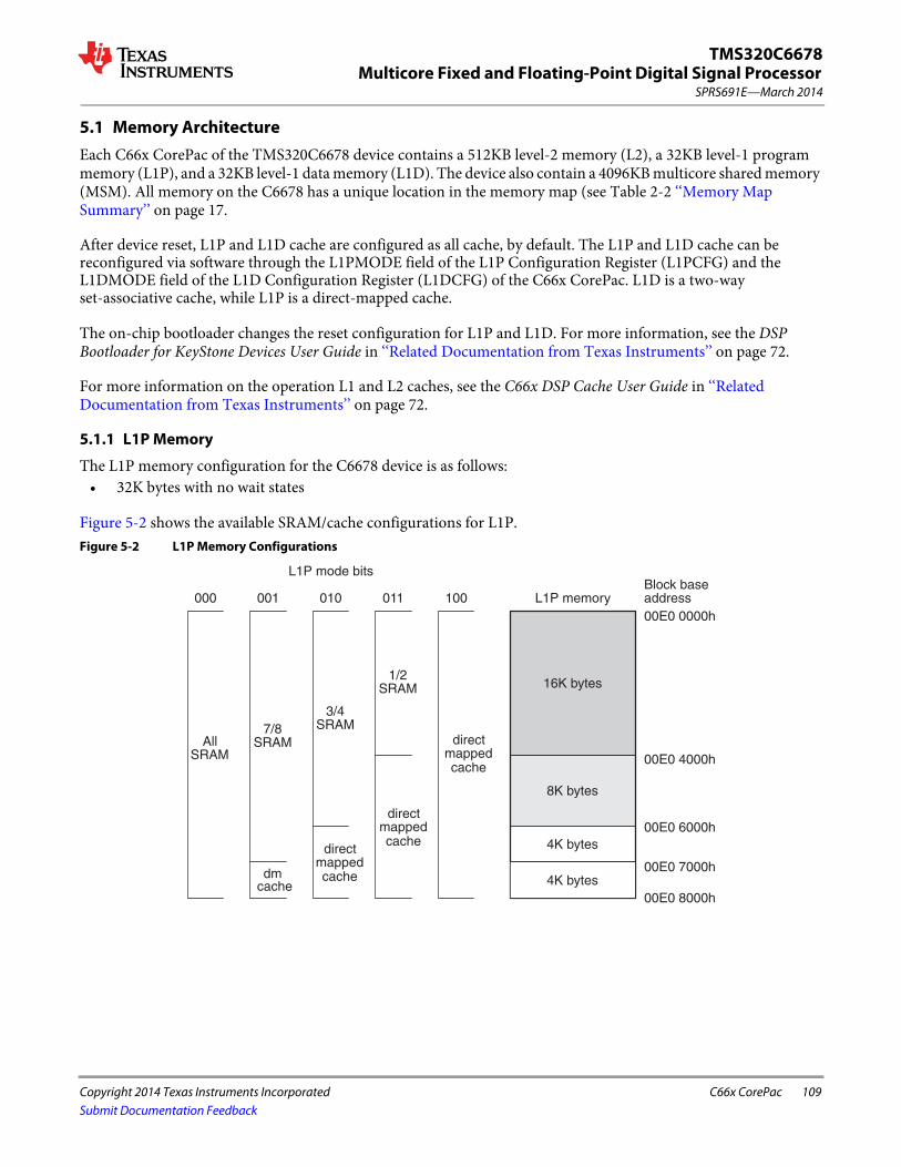
Multicore Fixed and Floating-Point Digital Signal Processor
Copyright 2014 Texas Instruments Incorporated C66x CorePac 109
SPRS691E—March 2014
TMS320C6678
Submit Documentation Feedback
5.1 Memory Architecture Each C66x CorePac of the TMS320C6678 device contains a 512KB level-2 memory (L2), a 32KB level-1 program memory (L1P), and a 32KB level-1 data memory (L1D). The device also contain a 4096KB multicore shared memory (MSM). All memory on the C6678 has a unique location in the memory map (see Table 2-2 ‘‘Memory Map Summary’’ on page 17.
After device reset, L1P and L1D cache are configured as all cache, by default. The L1P and L1D cache can be reconfigured via software through the L1PMODE field of the L1P Configuration Register (L1PCFG) and the L1DMODE field of the L1D Configuration Register (L1DCFG) of the C66x CorePac. L1D is a two-way set-associative cache, while L1P is a direct-mapped cache.
The on-chip bootloader changes the reset configuration for L1P and L1D. For more information, see the DSP Bootloader for KeyStone Devices User Guide in ‘‘Related Documentation from Texas Instruments’’ on page 72.
For more information on the operation L1 and L2 caches, see the C66x DSP Cache User Guide in ‘‘Related Documentation from Texas Instruments’’ on page 72.
5.1.1 L1P Memory
The L1P memory configuration for the C6678 device is as follows: • 32K bytes with no wait states
Figure 5-2 shows the available SRAM/cache configurations for L1P. Figure 5-2 L1P Memory Configurations
4K bytes
8K bytes
16K bytes
L1P memory00E0 0000h
00E0 4000h
00E0 6000h
00E0 7000h
00E0 8000h
directmapped
SRAM1/2
dm
3/4SRAM
SRAM7/8
AllSRAM
000 001 010 011 100Block baseaddress
L1P mode bits
cache 4K bytescache
directmappedcache
directmappedcache

110 C66x CorePac Copyright 2014 Texas Instruments Incorporated
SPRS691E—March 2014Multicore Fixed and Floating-Point Digital Signal ProcessorTMS320C6678
Submit Documentation Feedback
5.1.2 L1D Memory
The L1D memory configuration for the C6678 device is as follows:• 32K bytes with no wait states
Figure 5-3 shows the available SRAM/cache configurations for L1D. Figure 5-3 L1D Memory Configurations
4K bytes
8K bytes
16K bytes
L1D memory00F0 0000h
00F0 4000h
00F0 6000h
00F0 7000h
00F0 8000h
2-way
SRAM1/2
2-way
3/4SRAM
SRAM7/8
AllSRAM
000 001 010 011 100Block baseaddress
L1D mode bits
cache 4K bytescache
2-waycache
2-waycache
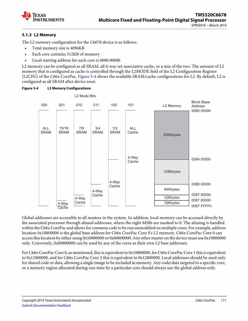
Multicore Fixed and Floating-Point Digital Signal Processor
Copyright 2014 Texas Instruments Incorporated C66x CorePac 111
SPRS691E—March 2014
TMS320C6678
Submit Documentation Feedback
5.1.3 L2 Memory
The L2 memory configuration for the C6678 device is as follows: • Total memory size is 4096KB • Each core contains 512KB of memory• Local starting address for each core is 0080 0000h
L2 memory can be configured as all SRAM, all 4-way set-associative cache, or a mix of the two. The amount of L2 memory that is configured as cache is controlled through the L2MODE field of the L2 Configuration Register (L2CFG) of the C66x CorePac. Figure 5-4 shows the available SRAM/cache configurations for L2. By default, L2 is configured as all SRAM after device reset. Figure 5-4 L2 Memory Configurations
Global addresses are accessible to all masters in the system. In addition, local memory can be accessed directly by the associated processor through aliased addresses, where the eight MSBs are masked to 0. The aliasing is handled within the C66x CorePac and allows for common code to be run unmodified on multiple cores. For example, address location 0x10800000 is the global base address for C66x CorePac Core 0's L2 memory. C66x CorePac Core 0 can access this location by either using 0x10800000 or 0x00800000. Any other master on the device must use 0x10800000 only. Conversely, 0x00800000 can by used by any of the cores as their own L2 base addresses.
For C66x CorePac Core 0, as mentioned, this is equivalent to 0x10800000, for C66x CorePac Core 1 this is equivalent to 0x11800000, and for C66x CorePac Core 2 this is equivalent to 0x12800000. Local addresses should be used only for shared code or data, allowing a single image to be included in memory. Any code/data targeted to a specific core, or a memory region allocated during run-time by a particular core should always use the global address only.
L2 Memory
0084 0000h
0086 0000h
0087 0000h
0087 8000h
0087 FFFFh
000 001 010 011 100Block BaseAddress
L2 Mode Bits
1/2SRAM
4-WayCache
101
0080 0000h
4-WayCache4-Way
Cache
ALLSRAM
4-WayCache
4-WayCache
3/4SRAM
7/8SRAM
15/16SRAM
256Kbytes
128Kbytes
64Kbytes
32Kbytes
32Kbytes
ALLCache

112 C66x CorePac Copyright 2014 Texas Instruments Incorporated
SPRS691E—March 2014Multicore Fixed and Floating-Point Digital Signal ProcessorTMS320C6678
Submit Documentation Feedback
5.1.4 MSM SRAM
The MSM SRAM configuration for the C6678 device is as follows: • Memory size is 4096KB • The MSM SRAM can be configured as shared L2 and/or shared L3 memory• Allows extension of external addresses from 2GB to up to 8GB• Has built in memory protection features
The MSM SRAM is always configured as all SRAM. When configured as a shared L2, its contents can be cached in L1P and L1D. When configured in shared L3 mode, it’s contents can be cached in L2 also. For more details on external memory address extension and memory protection features, see the Multicore Shared Memory Controller (MSMC) for KeyStone Devices User Guide in ‘‘Related Documentation from Texas Instruments’’ on page 72.
5.1.5 L3 Memory
The L3 ROM on the device is 128KB. The ROM contains software used to boot the device. There is no requirement to block accesses from this portion to the ROM.
Multicore Fixed and Floating-Point Digital Signal Processor
Copyright 2014 Texas Instruments Incorporated C66x CorePac 113
SPRS691E—March 2014
TMS320C6678
Submit Documentation Feedback
5.2 Memory ProtectionMemory protection allows an operating system to define who or what is authorized to access L1D, L1P, and L2 memory. To accomplish this, the L1D, L1P, and L2 memories are divided into pages. There are 16 pages of L1P (2KB each), 16 pages of L1D (2KB each), and 32 pages of L2 (16KB each). The L1D, L1P, and L2 memory controllers in the C66x CorePac are equipped with a set of registers that specify the permissions for each memory page.
Each page may be assigned with fully orthogonal user and supervisor read, write, and execute permissions. In addition, a page may be marked as either (or both) locally accessible or globally accessible. A local access is a direct DSP access to L1D, L1P, and L2, while a global access is initiated by a DMA (either IDMA or the EDMA3) or by other system masters. Note that EDMA or IDMA transfers programmed by the DSP count as global accesses. On a secure device, pages can be restricted to secure access only (default) or opened up for public, non-secure access.
The DSP and each of the system masters on the device are all assigned a privilege ID. It is possible to specify whether memory pages are locally or globally accessible.
The AIDx and LOCAL bits of the memory protection page attribute registers specify the memory page protection scheme, see Table 5-1.
Faults are handled by software in an interrupt (or an exception, programmable within the C66x CorePac interrupt controller) service routine. A DSP or DMA access to a page without the proper permissions will:
• Block the access — reads return 0, writes are ignored• Capture the initiator in a status register — ID, address, and access type are stored• Signal event to DSP interrupt controller
The software is responsible for taking corrective action to respond to the event and resetting the error status in the memory controller. For more information on memory protection for L1D, L1P, and L2, see the C66x DSP CorePac User Guide in ‘‘Related Documentation from Texas Instruments’’ on page 72.
Table 5-1 Available Memory Page Protection Schemes
AIDx Bit Local Bit Description
0 0 No access to memory page is permitted.
0 1 Only direct access by DSP is permitted.
1 0 Only accesses by system masters and IDMA are permitted (includes EDMA and IDMA accesses initiated by the DSP).
1 1 All accesses permitted.
End of Table 5-1

114 C66x CorePac Copyright 2014 Texas Instruments Incorporated
SPRS691E—March 2014Multicore Fixed and Floating-Point Digital Signal ProcessorTMS320C6678
Submit Documentation Feedback
5.3 Bandwidth Management When multiple requestors contend for a single C66x CorePac resource, the conflict is resolved by granting access to the highest priority requestor. The following four resources are managed by the Bandwidth Management control hardware:
• Level 1 Program (L1P) SRAM/Cache • Level 1 Data (L1D) SRAM/Cache • Level 2 (L2) SRAM/Cache • Memory-mapped registers configuration bus
The priority level for operations initiated within the C66x CorePac are declared through registers in the C66x CorePac. These operations are:
• DSP-initiated transfers• User-programmed cache coherency operations• IDMA-initiated transfers
The priority level for operations initiated outside the C66x CorePac by system peripherals is declared through the Priority Allocation Register (PRI_ALLOC), see section 4.3 ‘‘Bus Priorities’’ on page 107 for more details. System peripherals with no fields in the PRI_ALLOC have their own registers to program their priorities.
More information on the bandwidth management features of the C66x CorePac can be found in the C66x DSP CorePac User Guide in ‘‘Related Documentation from Texas Instruments’’ on page 72.
5.4 Power-Down ControlThe C66x CorePac supports the ability to power down various parts of the C66x CorePac. The power down controller (PDC) of the C66x CorePac can be used to power down L1P, the cache control hardware, the DSP, and the entire C66x CorePac. These power-down features can be used to design systems for lower overall system power requirements.
Note—The C6678 does not support power-down modes for the L2 memory at this time.
More information on the power-down features of the C66x CorePac can be found in the C66x DSP CorePac User Guide in ‘‘Related Documentation from Texas Instruments’’ on page 72.

Multicore Fixed and Floating-Point Digital Signal Processor
Copyright 2014 Texas Instruments Incorporated C66x CorePac 115
SPRS691E—March 2014
TMS320C6678
Submit Documentation Feedback
5.5 C66x CorePac Revision The version and revision of the C66x CorePac can be read from the CorePac Revision ID Register (MM_REVID) located at address 0181 2000h. The MM_REVID register is shown in Figure 5-5 and described in Table 5-2. The C66x CorePac revision is dependant on the silicon revision being used.
5.6 C66x CorePac Register DescriptionsSee the C66x DSP CorePac User Guide in ‘‘Related Documentation from Texas Instruments’’ on page 72 for register offsets and definitions.
Figure 5-5 CorePac Revision ID Register (MM_REVID) Address - 0181 2000h
31 16 15 0
VERSION REVISION
R-n R-n
Legend: R = Read; -n = value after reset
Table 5-2 CorePac Revision ID Register (MM_REVID) Field Descriptions
Bit Field Description
31-16 VERSION Version of the C66x CorePac implemented on the device.
15-0 REVISION Revision of the C66x CorePac version implemented on the device.
End of Table 5-2

116 Device Operating Conditions Copyright 2014 Texas Instruments Incorporated
SPRS691E—March 2014Multicore Fixed and Floating-Point Digital Signal ProcessorTMS320C6678
Submit Documentation Feedback
6 Device Operating Conditions
6.1 Absolute Maximum Ratings
Table 6-1 Absolute Maximum Ratings (1)
Over Operating Case Temperature Range (Unless Otherwise Noted)
1 Stresses beyond those listed under "absolute maximum ratings" may cause permanent damage to the device. These are stress ratings only, and functional operation of the device at these or any other conditions beyond those indicated under "recommended operating conditions" is not implied. Exposure to absolute-maximum-rated conditions for extended periods may affect device reliability.
Supply voltage range (2):
2 All voltage values are with respect to VSS.
CVDD -0.3 V to 1.3 V
CVDD1 -0.3 V to 1.3 V
DVDD15 -0.3 V to 2.45 V
DVDD18 -0.3 V to 2.45 V
VREFSSTL 0.49 × DVDD15 to 0.51 × DVDD15
VDDT1, VDDT2 -0.3 V to 1.3 V
VDDR1, VDDR2, VDDR3, VDDR4 -0.3 V to 2.45 V
AVDDA1, AVDDA2, AVDDA3 -0.3 V to 2.45 V
VSS Ground 0 V
Input voltage (VI) range:
LVCMOS (1.8V) -0.3 V to DVDD18+0.3 V
DDR3 -0.3 V to 2.45 V
I2C -0.3 V to 2.45 V
LVDS -0.3 V to DVDD18+0.3 V
LJCB -0.3 V to 1.3 V
SerDes -0.3 V to CVDD1+0.3 V
Output voltage (VO) range:
LVCMOS (1.8V) -0.3 V to DVDD18+0.3 V
DDR3 -0.3 V to 2.45 V
I2C -0.3 V to 2.45 V
SerDes -0.3 V to CVDD1+0.3 V
Operating case temperature range, TC: Commercial 0°C to 85°C
Extended -40°C to 100°C
ESD stress voltage, VESD (3):
3 Electrostatic discharge (ESD) to measure device sensitivity/immunity to damage caused by electrostatic discharges into the device.
HBM (human body model) (4)
4 Level listed above is the passing level per ANSI/ESDA/JEDEC JS-001-2010. JEDEC document JEP155 states that 500 V HBM allows safe manufacturing with a standard ESD control process, and manufacturing with less than 500 V HBM is possible if necessary precautions are taken. Pins listed as 1000 V may actually have higher performance.
±1000 V
CDM (charged device model) (5)
5 Level listed above is the passing level per EIA-JEDEC JESD22-C101E. JEDEC document JEP157 states that 250 V CDM allows safe manufacturing with a standard ESD control process. Pins listed as 250 V may actually have higher performance.
±250 V
Overshoot/undershoot (6)
6 Overshoot/Undershoot percentage relative to I/O operating values - for example the maximum overshoot value for 1.8-V LVCMOS signals is DVDD18 + 0.20 × DVDD18 and maximum undershoot value would be VSS - 0.20 × DVDD18
LVCMOS (1.8V)20% Overshoot/Undershoot for 20% of
Signal Duty CycleDDR3
I2C
Storage temperature range, Tstg: -65°C to 150°C
End of Table 6-1

Multicore Fixed and Floating-Point Digital Signal Processor
Copyright 2014 Texas Instruments Incorporated Device Operating Conditions 117
SPRS691E—March 2014
TMS320C6678
Submit Documentation Feedback
6.2 Recommended Operating Conditions
Table 6-2 Recommended Operating Conditions (1) (2)
1 All differential clock inputs comply with the LVDS Electrical Specification, IEEE 1596.3-1996 and all SerDes I/Os comply with the XAUI Electrical Specification, IEEE 802.3ae-2002.
2 All SerDes I/Os comply with the XAUI Electrical Specification, IEEE 802.3ae-2002.
Min Nom Max Unit
CVDD SR Core Supply
Initial Startup VINITnom × 0.95 1.1or 1.15 (3)
3 The initial CVDD voltage at power on must be 1.1 V nominal (for 1000-MHz and 1250-MHz devices) or 1.15 V nominal (for 1400-MHz device) and it must transition to the VID set value immediately after being presented on the VCNTL pins. This is required to maintain full-power functionality and reliability targets specified by TI.
VINITnom × 1.05
V1000MHz - Device SRVnom (4) × 0.95
4 SRVnom refers to the unique SmartReflex core supply voltage set from the factory for each individual device.
0.85-1.1 SRVnom × 1.05
1250MHz - Device SRVnom × 0.95 0.9-1.1 SRVnom × 1.05
1400MHz - Device SRVnom × 0.95 0.95-1.15 SRVnom × 1.05
CVDD1 Core supply voltage for memory array 0.95 1 1.05 V
DVDD18 1.8-V supply I/O voltage 1.71 1.8 1.89 V
DVDD15 1.5-V supply I/O voltage 1.425 1.5 1.575 V
VREFSSTL DDR3 reference voltage 0.49 × DVDD15 0.5 × DVDD15 0.51 × DVDD15 V
VDDRx (5)
5 Where x = 1, 2, 3, 4... to indicate all supplies of the same kind.
SerDes regulator supply 1.425 1.5 1.575 V
VDDAx PLL analog supply 1.71 1.8 1.89 V
VDDTx SerDes termination supply 0.95 1 1.05 V
VSS Ground 0 0 0 V
VIH High-level input voltage
LVCMOS (1.8 V) 0.65 × DVDD18 V
I2C 0.7 × DVDD18 V
DDR3 EMIF VREFSSTL + 0.1 V
VIL Low-level input voltage
LVCMOS (1.8 V) 0.35 × DVDD18 V
DDR3 EMIF -0.3 VREFSSTL - 0.1 V
I2C 0.3 × DVDD18 V
TC Operating case temperature Commercial 0 85 °C
Extended -40 100 °C
End of Table 6-2
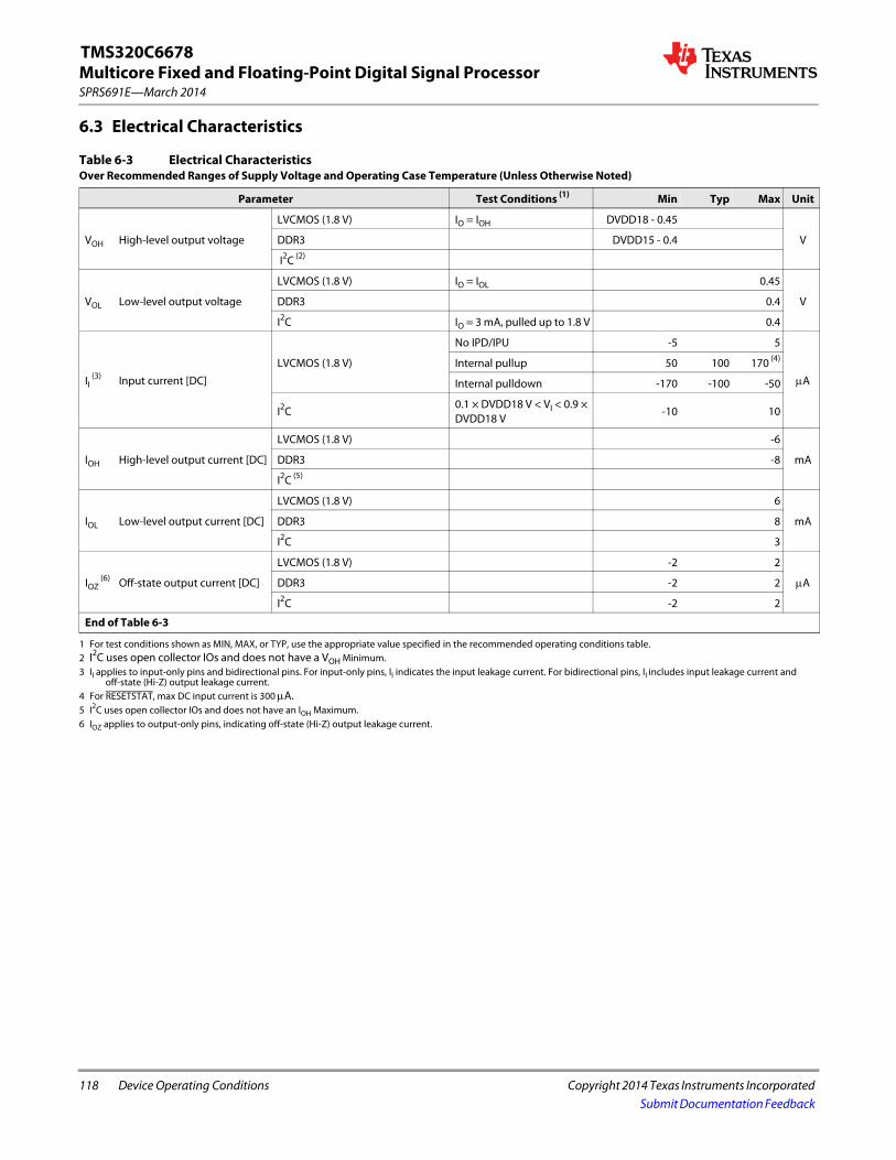
118 Device Operating Conditions Copyright 2014 Texas Instruments Incorporated
SPRS691E—March 2014Multicore Fixed and Floating-Point Digital Signal ProcessorTMS320C6678
Submit Documentation Feedback
6.3 Electrical Characteristics
Table 6-3 Electrical Characteristics Over Recommended Ranges of Supply Voltage and Operating Case Temperature (Unless Otherwise Noted)
Parameter Test Conditions (1)
1 For test conditions shown as MIN, MAX, or TYP, use the appropriate value specified in the recommended operating conditions table.
Min Typ Max Unit
VOH High-level output voltage
LVCMOS (1.8 V) IO = IOH DVDD18 - 0.45
VDDR3 DVDD15 - 0.4
I2C (2)
2 I2C uses open collector IOs and does not have a VOH Minimum.
VOL Low-level output voltage
LVCMOS (1.8 V) IO = IOL 0.45
VDDR3 0.4
I2C IO = 3 mA, pulled up to 1.8 V 0.4
II (3)
3 II applies to input-only pins and bidirectional pins. For input-only pins, II indicates the input leakage current. For bidirectional pins, II includes input leakage current and off-state (Hi-Z) output leakage current.
Input current [DC]
LVCMOS (1.8 V)
No IPD/IPU -5 5
A
Internal pullup 50 100 170 (4)
4 For RESETSTAT, max DC input current is 300 A.
Internal pulldown -170 -100 -50
I2C0.1 × DVDD18 V < VI < 0.9 × DVDD18 V
-10 10
IOH High-level output current [DC]
LVCMOS (1.8 V) -6
mADDR3 -8
I2C (5)
5 I2C uses open collector IOs and does not have an IOH Maximum.
IOL Low-level output current [DC]
LVCMOS (1.8 V) 6
mA DDR3 8
I2C 3
IOZ (6)
6 IOZ applies to output-only pins, indicating off-state (Hi-Z) output leakage current.
Off-state output current [DC]
LVCMOS (1.8 V) -2 2
A DDR3 -2 2
I2C -2 2
End of Table 6-3

Multicore Fixed and Floating-Point Digital Signal Processor
Copyright 2014 Texas Instruments Incorporated Device Operating Conditions 119
SPRS691E—March 2014
TMS320C6678
Submit Documentation Feedback
6.4 Power Supply to Peripheral I/O Mapping
Table 6-4 Power Supply to Peripheral I/O Mapping (1) (2)
Over Recommended Ranges of Supply Voltage and Operating Case Temperature (Unless Otherwise Noted)
1 Note that this table does not attempt to describe all functions of all power supply terminals, but only those whose purpose it is to power peripheral I/O buffers and clock input buffers.
2 See the Hardware Design Guide for KeyStone I Devices in ‘‘Related Documentation from Texas Instruments’’ on page 72 for more information about individual peripheral I/O.
Power Supply I/O Buffer Type Associated Peripheral
CVDD Supply Core Voltage LJCB
CORECLK(P|N) PLL input buffers
SRIOSGMIICLK(P|N) SerDes PLL input buffers
DDRCLK(P|N) PLL input buffers
PCIECLK(P|N) SerDes PLL input buffers
MCMCLK(P|N) SerDes PLL input buffers
PASSCLK(P|N) PLL input buffers
DVDD15 1.5-V supply I/O voltage DDR3 (1.5 V) All DDR3 memory controller peripheral I/O buffers
DVDD18 1.8-V supply I/O voltage
LVCMOS (1.8 V)
All GPIO peripheral I/O buffers
All JTAG and EMU peripheral I/O buffers
All Timer peripheral I/O buffers
All SPI peripheral I/O buffers
All RESETs, NMI, Control peripheral I/O buffers
All Hyperlink sideband peripheral I/O buffers
All MDIO peripheral I/O buffers
All UART peripheral I/O buffers
All TSIP0 and TSIP1 peripheral I/O buffers
All EMIF16 peripheral I/O buffers
Open-drain (1.8V)All I2C peripheral I/O buffers
All SmartReflex peripheral I/O buffers
VDDT1 Hyperlink SerDes termination and analog front-end supply SerDes/CML Hyperlink SerDes CML IO buffers
VDDT2 SRIO/SGMII/PCIE SerDes termination and analog front-end supply SerDes/CML SRIO/SGMII/PCIE SerDes CML IO buffers
End of Table 6-4

120 Peripheral Information and Electrical Specifications Copyright 2014 Texas Instruments Incorporated
SPRS691E—March 2014Multicore Fixed and Floating-Point Digital Signal ProcessorTMS320C6678
Submit Documentation Feedback
7 Peripheral Information and Electrical SpecificationsThis chapter covers the various peripherals on the TMS320C6678 DSP. Peripheral-specific information, timing diagrams, electrical specifications, and register memory maps are described in this chapter.
7.1 Parameter Information This section describes the conditions used to capture the electrical data seen in this chapter.
7.1.1 Timing Parameters and Board Routing Analysis
The timing parameter values specified in this data manual do not include delays caused by board routings. As a good board design practice, such delays must always be taken into account. Timing values may be adjusted by increasing/decreasing such delays. TI recommends using the available I/O buffer information specification (IBIS) models to analyze the timing characteristics correctly. To properly use IBIS models to attain accurate timing analysis for a given system, see the Using IBIS Models for Timing Analysis application report in ‘‘Related Documentation from Texas Instruments’’ on page 72. If needed, external logic hardware such as buffers may be used to compensate any timing differences.
7.1.2 1.8-V LVCMOS Signal Transition Levels
All input and output timing parameters are referenced to VDD/2 for both 0 and 1 logic levels.Figure 7-1 Input and Output Voltage Reference Levels for AC Timing Measurements
All rise and fall transition timing parameters are referenced to VIL MAX and VIH MIN for input clocks, VOL MAX and VOH MIN for output clocks. Figure 7-2 Rise and Fall Transition Time Voltage Reference Levels
7.2 Recommended Clock and Control Signal Transition BehaviorAll clocks and control signals must transition between VIH and VIL (or between VIL and VIH) in a monotonic manner.
V = VDD / 2ref
V = V MIN (or V MIN)ref IH OH
V = V MAX (or V MAX)ref IL OL
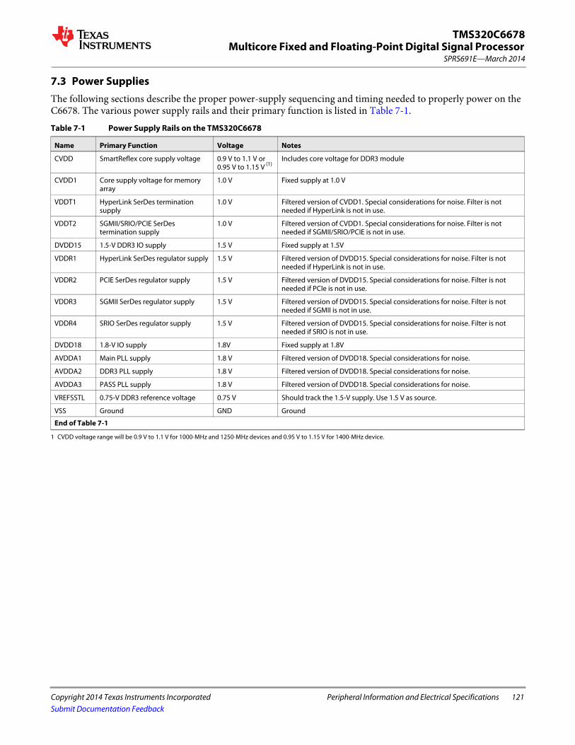
Multicore Fixed and Floating-Point Digital Signal Processor
Copyright 2014 Texas Instruments Incorporated Peripheral Information and Electrical Specifications 121
SPRS691E—March 2014
TMS320C6678
Submit Documentation Feedback
7.3 Power SuppliesThe following sections describe the proper power-supply sequencing and timing needed to properly power on the C6678. The various power supply rails and their primary function is listed in Table 7-1.Table 7-1 Power Supply Rails on the TMS320C6678
Name Primary Function Voltage Notes
CVDD SmartReflex core supply voltage 0.9 V to 1.1 V or 0.95 V to 1.15 V (1)
1 CVDD voltage range will be 0.9 V to 1.1 V for 1000-MHz and 1250-MHz devices and 0.95 V to 1.15 V for 1400-MHz device.
Includes core voltage for DDR3 module
CVDD1 Core supply voltage for memory array
1.0 V Fixed supply at 1.0 V
VDDT1 HyperLink SerDes termination supply
1.0 V Filtered version of CVDD1. Special considerations for noise. Filter is not needed if HyperLink is not in use.
VDDT2 SGMII/SRIO/PCIE SerDes termination supply
1.0 V Filtered version of CVDD1. Special considerations for noise. Filter is not needed if SGMII/SRIO/PCIE is not in use.
DVDD15 1.5-V DDR3 IO supply 1.5 V Fixed supply at 1.5V
VDDR1 HyperLink SerDes regulator supply 1.5 V Filtered version of DVDD15. Special considerations for noise. Filter is not needed if HyperLink is not in use.
VDDR2 PCIE SerDes regulator supply 1.5 V Filtered version of DVDD15. Special considerations for noise. Filter is not needed if PCIe is not in use.
VDDR3 SGMII SerDes regulator supply 1.5 V Filtered version of DVDD15. Special considerations for noise. Filter is not needed if SGMII is not in use.
VDDR4 SRIO SerDes regulator supply 1.5 V Filtered version of DVDD15. Special considerations for noise. Filter is not needed if SRIO is not in use.
DVDD18 1.8-V IO supply 1.8V Fixed supply at 1.8V
AVDDA1 Main PLL supply 1.8 V Filtered version of DVDD18. Special considerations for noise.
AVDDA2 DDR3 PLL supply 1.8 V Filtered version of DVDD18. Special considerations for noise.
AVDDA3 PASS PLL supply 1.8 V Filtered version of DVDD18. Special considerations for noise.
VREFSSTL 0.75-V DDR3 reference voltage 0.75 V Should track the 1.5-V supply. Use 1.5 V as source.
VSS Ground GND Ground
End of Table 7-1
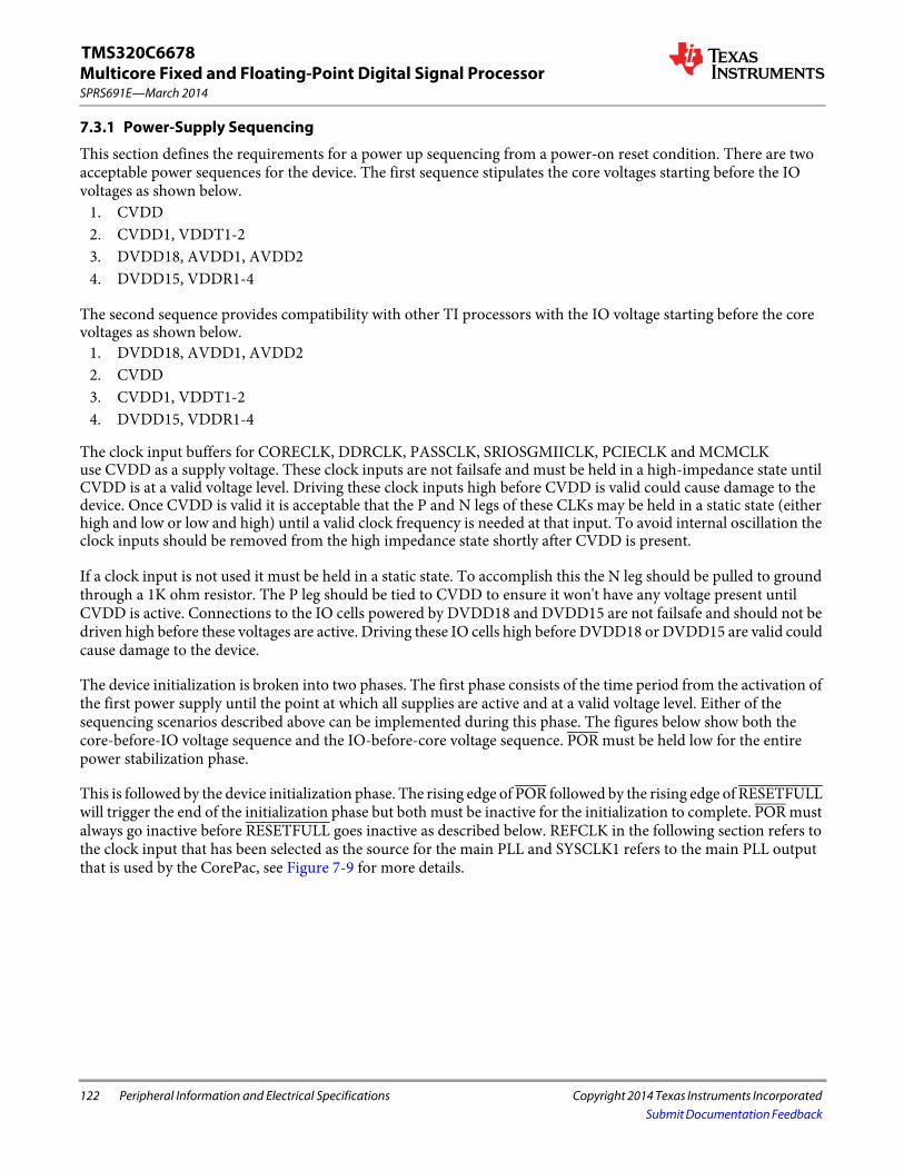
122 Peripheral Information and Electrical Specifications Copyright 2014 Texas Instruments Incorporated
SPRS691E—March 2014Multicore Fixed and Floating-Point Digital Signal ProcessorTMS320C6678
Submit Documentation Feedback
7.3.1 Power-Supply Sequencing
This section defines the requirements for a power up sequencing from a power-on reset condition. There are two acceptable power sequences for the device. The first sequence stipulates the core voltages starting before the IO voltages as shown below.
1. CVDD 2. CVDD1, VDDT1-23. DVDD18, AVDD1, AVDD24. DVDD15, VDDR1-4
The second sequence provides compatibility with other TI processors with the IO voltage starting before the core voltages as shown below.
1. DVDD18, AVDD1, AVDD22. CVDD 3. CVDD1, VDDT1-24. DVDD15, VDDR1-4
The clock input buffers for CORECLK, DDRCLK, PASSCLK, SRIOSGMIICLK, PCIECLK and MCMCLK use CVDD as a supply voltage. These clock inputs are not failsafe and must be held in a high-impedance state until CVDD is at a valid voltage level. Driving these clock inputs high before CVDD is valid could cause damage to the device. Once CVDD is valid it is acceptable that the P and N legs of these CLKs may be held in a static state (either high and low or low and high) until a valid clock frequency is needed at that input. To avoid internal oscillation the clock inputs should be removed from the high impedance state shortly after CVDD is present.
If a clock input is not used it must be held in a static state. To accomplish this the N leg should be pulled to ground through a 1K ohm resistor. The P leg should be tied to CVDD to ensure it won't have any voltage present until CVDD is active. Connections to the IO cells powered by DVDD18 and DVDD15 are not failsafe and should not be driven high before these voltages are active. Driving these IO cells high before DVDD18 or DVDD15 are valid could cause damage to the device.
The device initialization is broken into two phases. The first phase consists of the time period from the activation of the first power supply until the point at which all supplies are active and at a valid voltage level. Either of the sequencing scenarios described above can be implemented during this phase. The figures below show both the core-before-IO voltage sequence and the IO-before-core voltage sequence. POR must be held low for the entire power stabilization phase.
This is followed by the device initialization phase. The rising edge of POR followed by the rising edge of RESETFULL will trigger the end of the initialization phase but both must be inactive for the initialization to complete. POR must always go inactive before RESETFULL goes inactive as described below. REFCLK in the following section refers to the clock input that has been selected as the source for the main PLL and SYSCLK1 refers to the main PLL output that is used by the CorePac, see Figure 7-9 for more details.

Multicore Fixed and Floating-Point Digital Signal Processor
Copyright 2014 Texas Instruments Incorporated Peripheral Information and Electrical Specifications 123
SPRS691E—March 2014
TMS320C6678
Submit Documentation Feedback
7.3.1.1 Core-Before-IO Power Sequencing
Figure 7-3 shows the power sequencing and reset control of TMS320C6678 for device initialization. POR may be removed after the power has been stable for the required 100 μsec. RESETFULL must be held low for a period after the rising edge of POR but may be held low for longer periods if necessary. The configuration bits shared with the GPIO pins will be latched on the rising edge of RESETFULL and must meet the setup and hold times specified. REFCLK must always be active before POR can be removed. Core-before-IO power sequencing is defined in Table 7-2.
Note—TI recommends a maximum of 100 ms between one power rail being valid, and the next power rail in the sequence starting to ramp. Each supply must ramp monotonically and must reach a stable valid level within 20ms.
Figure 7-3 Core Before IO Power Sequencing
RESET
RESETFULL
POR
CVDD
CVDD1
DVDD18
DVDD15
REFCLKP&N
DDRCLKP&N
RESETSTAT
Power Stabilization Phase Device Initialization Phase
6
5
4a
4b
2a
3
2c
GPIO ConfigBits
8
7
9 10
2b
1

124 Peripheral Information and Electrical Specifications Copyright 2014 Texas Instruments Incorporated
SPRS691E—March 2014Multicore Fixed and Floating-Point Digital Signal ProcessorTMS320C6678
Submit Documentation Feedback
Table 7-2 Core Before IO Power Sequencing
Time System State
1 Begin Power Stabilization Phase • CVDD (core AVS) ramps up. • POR must be held low through the power stabilization phase. Because POR is low, all the core logic that has async reset (created from
POR) is put into the reset state.• Once enabled, the power supply should ramp to its valid voltage level within 20 ms.
2a • CVDD1 (core constant) ramps at the same time or shortly following CVDD. Although ramping CVDD1 and CVDD simultaneously is permitted, the voltage for CVDD1 must never exceed CVDD until after CVDD has reached a valid voltage.
• The purpose of ramping up the core supplies close to each other is to reduce crowbar current. CVDD1 should trail CVDD as this will ensure that the WLs in the memories are turned off and there is no current through the memory bit cells. If, however, CVDD1 (core constant) ramps up before CVDD (core AVS), then the worst-case current could be on the order of twice the specified draw of CVDD1.
• The maximum duration is 100 ms.
2b • Once CVDD is valid, the clock drivers should be enabled. Although the clock inputs are not necessary at this time, they should either be driven with a valid clock or be held in a static state with one leg high and one leg low.
2c • The DDRCLK and REFCLK may begin to toggle anytime between when CVDD is at a valid level and the setup time before POR goes high specified by t6.
3 • Filtered versions of 1.8 V can ramp simultaneously with DVDD18. • RESETSTAT is driven low once the DVDD18 supply is available.• All LVCMOS input and bidirectional pins must not be driven or pulled high until DVDD18 is present. Driving an input or bidirectional pin
before DVDD18 is valid could cause damage to the device.
4a • DVDD15 (1.5 V) supply is ramped up after DVDD18 is valid. Although ramping DVDD18 and DVDD15 simultaneously is permitted, the voltage for DVDD15 must never exceed DVDD18.
4b • RESET may be driven high any time after DVDD18 is at a valid level. In a POR-controlled boot, RESET must be high before POR is driven high.
5 • POR must continue to remain low for at least 100 μs after power has stabilized.
End Power Stabilization Phase
6 • Device initialization requires 500 REFCLK periods after the Power Stabilization Phase. The maximum clock period is 33.33 nsec, so a delay of an additional 16 μs is required before a rising edge of POR. The clock must be active during the entire 16 μs.
7 • RESETFULL must be held low for at least 24 transitions of the REFCLK after POR has stabilized at a high level.
8 • The rising edge of the RESETFULL will remove the reset to the efuse farm allowing the scan to begin.• Once device initialization and the efuse farm scan are complete, the RESETSTAT signal is driven high. This delay will be 10000 to 50000
clock cycles.
End Device Initialization Phase
9 • GPIO configuration bits must be valid for at least 12 transitions of the REFCLK before the rising edge of RESETFULL
10 • GPIO configuration bits must be held valid for at least 12 transitions of the REFCLK after the rising edge of RESETFULL
End of Table 7-2

Multicore Fixed and Floating-Point Digital Signal Processor
Copyright 2014 Texas Instruments Incorporated Peripheral Information and Electrical Specifications 125
SPRS691E—March 2014
TMS320C6678
Submit Documentation Feedback
7.3.1.2 IO-Before-Core Power Sequencing
The timing diagram for IO-before-core power sequencing is shown in Figure 7-4 and defined in Table 7-3.
Note—TI recommends a maximum of 100 ms between one power rail being valid, and the next power rail in the sequence starting to ramp. Each supply must ramp monotonically and must reach a stable valid level within 20 ms.
Figure 7-4 IO Before Core Power Sequencing
RESET
RESETFULL
1
POR
CVDD
CVDD1
DVDD18
DVDD15
REFCLKP&N
DDRCLKP&N
RESETSTAT
Power Stabilization Phase Device Initialization Phase
6
2a
2b
GPIO ConfigBits
8
7
9 10
3a
3b
3c
4
5
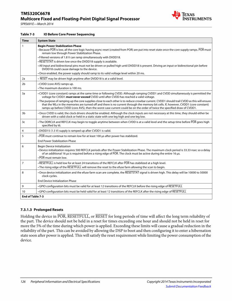
126 Peripheral Information and Electrical Specifications Copyright 2014 Texas Instruments Incorporated
SPRS691E—March 2014Multicore Fixed and Floating-Point Digital Signal ProcessorTMS320C6678
Submit Documentation Feedback
7.3.1.3 Prolonged Resets
Holding the device in POR, RESETFULL, or RESET for long periods of time will affect the long term reliability of the part. The device should not be held in a reset for times exceeding one hour and should not be held in reset for more the 5% of the time during which power is applied. Exceeding these limits will cause a gradual reduction in the reliability of the part. This can be avoided by allowing the DSP to boot and then configuring it to enter a hibernation state soon after power is applied. This will satisfy the reset requirement while limiting the power consumption of the device.
Table 7-3 IO Before Core Power Sequencing
Time System State
1 Begin Power Stabilization Phase • Because POR is low, all the core logic having async reset (created from POR) are put into reset state once the core supply ramps. POR must
remain low through Power Stabilization Phase. • Filtered versions of 1.8 V can ramp simultaneously with DVDD18. • RESETSTAT is driven low once the DVDD18 supply is available.• All input and bidirectional pins must not be driven or pulled high until DVDD18 is present. Driving an input or bidirectional pin before
DVDD18 could cause damage to the device.• Once enabled, the power supply should ramp to its valid voltage level within 20 ms.
2a • RESET may be driven high anytime after DVDD18 is at a valid level.
2b • CVDD (core AVS) ramps up.• The maximum duration is 100 ms.
3a • CVDD1 (core constant) ramps at the same time or following CVDD. Although ramping CVDD1 and CVDD simultaneously is permitted the voltage for CVDD1 must never exceed CVDD until after CVDD has reached a valid voltage.
• The purpose of ramping up the core supplies close to each other is to reduce crowbar current. CVDD1 should trail CVDD as this will ensure that the WLs in the memories are turned off and there is no current through the memory bit cells. If, however, CVDD1 (core constant) ramps up before CVDD (core AVS), then the worst case current could be on the order of twice the specified draw of CVDD1.
3b • Once CVDD is valid, the clock drivers should be enabled. Although the clock inputs are not necessary at this time, they should either be driven with a valid clock or held in a static state with one leg high and one leg low.
3c • The DDRCLK and REFCLK may begin to toggle anytime between when CVDD is at a valid level and the setup time before POR goes high specified by t6.
4 • DVDD15 (1.5 V) supply is ramped up after CVDD1 is valid.
5 • POR must continue to remain low for at least 100 μs after power has stabilized.
End Power Stabilization Phase
6 Begin Device Initialization• Device initialization requires 500 REFCLK periods after the Power Stabilization Phase. The maximum clock period is 33.33 nsec so a delay
of an additional 16 μs is required before a rising edge of POR. The clock must be active during the entire 16 μs. • POR must remain low.
7 • RESETFULL is held low for at least 24 transitions of the REFCLK after POR has stabilized at a high level.• The rising edge of the RESETFULL will remove the reset to the efuse farm allowing the scan to begin.
8 • Once device initialization and the efuse farm scan are complete, the RESETSTAT signal is driven high. This delay will be 10000 to 50000 clock cycles.
End Device Initialization Phase
9 • GPIO configuration bits must be valid for at least 12 transitions of the REFCLK before the rising edge of RESETFULL
10 • GPIO configuration bits must be held valid for at least 12 transitions of the REFCLK after the rising edge of RESETFULL
End of Table 7-3

Multicore Fixed and Floating-Point Digital Signal Processor
Copyright 2014 Texas Instruments Incorporated Peripheral Information and Electrical Specifications 127
SPRS691E—March 2014
TMS320C6678
Submit Documentation Feedback
7.3.1.4 Clocking During Power Sequencing
Some of the clock inputs are required to be present for the device to initialize correctly, but behavior of many of the clocks is contingent on the state of the boot configuration pins. Table 7-4 describes the clock sequencing and the conditions that affect the clock operation. Note that all clock drivers should be in a high-impedance state until CVDD is at a valid level and that all clock inputs either be active or in a static state with one leg pulled low and the other connected to CVDD.
7.3.2 Power-Down Sequence
The power down sequence is the exact reverse of the power-up sequence described above. The goal is to prevent a large amount of static current and to prevent overstress of the device. A power-good circuit that monitors all the supplies for the device should be used in all designs. If a catastrophic power supply failure occurs on any voltage rail, POR should transition to low to prevent over-current conditions that could possibly impact device reliability.
A system power monitoring solution is needed to shut down power to the board if a power supply fails. Long-term exposure to an environment in which one of the power supply voltages is no longer present will affect the reliability of the device. Holding the device in reset is not an acceptable solution because prolonged periods of time with an active reset can also affect long term reliability.
7.3.3 Power Supply Decoupling and Bulk Capacitors
In order to properly decouple the supply planes on the PCB from system noise, decoupling and bulk capacitors are required. Bulk capacitors are used to minimize the effects of low frequency current transients and decoupling or bypass capacitors are used to minimize higher frequency noise. For recommendations on selection of Power Supply Decoupling and Bulk capacitors see the Hardware Design Guide for KeyStone I Devices in ‘‘Related Documentation from Texas Instruments’’ on page 72.
Table 7-4 Clock Sequencing
Clock Condition Sequencing
DDRCLK None Must be present 16 μsec before POR transitions high.
CORECLK None CORECLK used to clock the core PLL. It must be present 16 μsec before POR transitions high.
PASSCLKPASSCLKSEL = 0 PASSCLK is not used and should be tied to a static state.
PASSCLKSEL = 1 PASSCLK is used as a source for the PASS PLL. It must be present before the PASS PLL is removed from reset and programmed.
SRIOSGMIICLK
An SGMII port will be used. SRIOSGMIICLK must be present 16 μsec before POR transitions high.
SGMII will not be used. SRIO will be used as a boot device.
SRIOSGMIICLK must be present 16 μsec before POR transitions high.
SGMII will not be used. SRIO will be used after boot.
SRIOSGMIICLK is used as a source to the SRIO SerDes PLL. It must be present before the SRIO is removed from reset and programmed.
SGMII will not be used. SRIO will not be used.
SRIOSGMIICLK is not used and should be tied to a static state.
PCIECLK
PCIE will be used as a boot device.
PCIECLK must be present 16 μsec before POR transitions high.
PCIE will be used after boot. PCIECLK is used as a source to the PCIE SerDes PLL. It must be present before the PCIE is removed from reset and programmed.
PCIE will not be used. PCIECLK is not used and should be tied to a static state.
MCMCLK
HyperLink will be used as a boot device.
MCMCLK must be present 16usec before POR transitions high.
HyperLink will be used after boot.
MCMCLK is used as a source to the MCM SerDes PLL. It must be present before the HyperLink is removed from reset and programmed.
HyperLink will not be used. MCMCLK is not used and should be tied to a static state.
End of Table 7-4
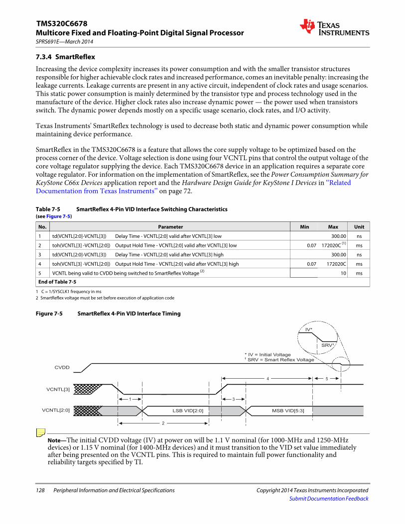
128 Peripheral Information and Electrical Specifications Copyright 2014 Texas Instruments Incorporated
SPRS691E—March 2014Multicore Fixed and Floating-Point Digital Signal ProcessorTMS320C6678
Submit Documentation Feedback
7.3.4 SmartReflex
Increasing the device complexity increases its power consumption and with the smaller transistor structures responsible for higher achievable clock rates and increased performance, comes an inevitable penalty: increasing the leakage currents. Leakage currents are present in any active circuit, independent of clock rates and usage scenarios. This static power consumption is mainly determined by the transistor type and process technology used in the manufacture of the device. Higher clock rates also increase dynamic power — the power used when transistors switch. The dynamic power depends mostly on a specific usage scenario, clock rates, and I/O activity.
Texas Instruments' SmartReflex technology is used to decrease both static and dynamic power consumption while maintaining device performance.
SmartReflex in the TMS320C6678 is a feature that allows the core supply voltage to be optimized based on the process corner of the device. Voltage selection is done using four VCNTL pins that control the output voltage of the core voltage regulator supplying the device. Each TMS320C6678 device in an application requires a separate core voltage regulator. For information on the implementation of SmartReflex, see the Power Consumption Summary for KeyStone C66x Devices application report and the Hardware Design Guide for KeyStone I Devices in ‘‘Related Documentation from Texas Instruments’’ on page 72.
Figure 7-5 SmartReflex 4-Pin VID Interface Timing
Note—The initial CVDD voltage (IV) at power on will be 1.1 V nominal (for 1000-MHz and 1250-MHz devices) or 1.15 V nominal (for 1400-MHz devices) and it must transition to the VID set value immediately after being presented on the VCNTL pins. This is required to maintain full power functionality and reliability targets specified by TI.
Table 7-5 SmartReflex 4-Pin VID Interface Switching Characteristics(see Figure 7-5)
No. Parameter Min Max Unit
1 td(VCNTL[2:0]-VCNTL[3]) Delay Time - VCNTL[2:0] valid after VCNTL[3] low 300.00 ns
2 toh(VCNTL[3] -VCNTL[2:0]) Output Hold Time - VCNTL[2:0] valid after VCNTL[3] low 0.07 172020C (1)
1 C = 1/SYSCLK1 frequency in ms
ms
3 td(VCNTL[2:0]-VCNTL[3]) Delay Time - VCNTL[2:0] valid after VCNTL[3] high 300.00 ns
4 toh(VCNTL[3] -VCNTL[2:0]) Output Hold Time - VCNTL[2:0] valid after VCNTL[3] high 0.07 172020C ms
5 VCNTL being valid to CVDD being switched to SmartReflex Voltage (2)
2 SmartReflex voltage must be set before execution of application code
10 ms
End of Table 7-5
VCNTL[2:0]
VCNTL[3]
1
2
4
LSB VID[2:0] MSB VID[5:3]
3
5
IV*
SRV†
CVDD
* IV = Initial VoltageSRV = Smart Reflex Voltage
†

Multicore Fixed and Floating-Point Digital Signal Processor
Copyright 2014 Texas Instruments Incorporated Peripheral Information and Electrical Specifications 129
SPRS691E—March 2014
TMS320C6678
Submit Documentation Feedback
7.4 Power Sleep Controller (PSC)The Power Sleep Controller (PSC) controls overall device power by turning off unused power domains and gating off clocks to individual peripherals and modules. The PSC provides the user with an interface to control several important power and clock operations.
For information on the Power Sleep Controller, see the Power Sleep Controller (PSC) for KeyStone Devices User Guide in ‘‘Related Documentation from Texas Instruments’’ on page 72.
7.4.1 Power Domains
The device has several power domains that can be turned on for operation or off to minimize power dissipation. The global power/sleep controller (GPSC) is used to control the power gating of various power domains.
Table 7-6 shows the TMS320C6678 power domains. Table 7-6 Power Domains
Domain Block(s) Note Power Connection
0 Most peripheral logic Cannot be disabled Always on
1 Per-core TETB and System TETB RAMs can be powered down Software control
2 Packet Coprocessor Logic can be powered down Software control
3 PCIe Logic can be powered down Software control
4 SRIO Logic can be powered down Software control
5 HyperLink Logic can be powered down Software control
6 Reserved Reserved Reserved
7 MSMC RAM MSMC RAM can be powered down Software control
8 C66x CorePac0, L1/L2 RAMs L2 RAMs can sleep
Software control via C66x core. For details, see the C66x DSP CorePac User Guide.
9 C66x CorePac1, L1/L2 RAMs L2 RAMs can sleep
10 C66x CorePac2, L1/L2 RAMs L2 RAMs can sleep
11 C66x CorePac3, L1/L2 RAMs L2 RAMs can sleep
12 C66x CorePac4, L1/L2 RAMs L2 RAMs can sleep
13 C66x CorePac5, L1/L2 RAMs L2 RAMs can sleep
14 C66x CorePac6, L1/L2 RAMs L2 RAMs can sleep
15 C66x CorePac7, L1/L2 RAMs L2 RAMs can sleep
End of Table 7-6
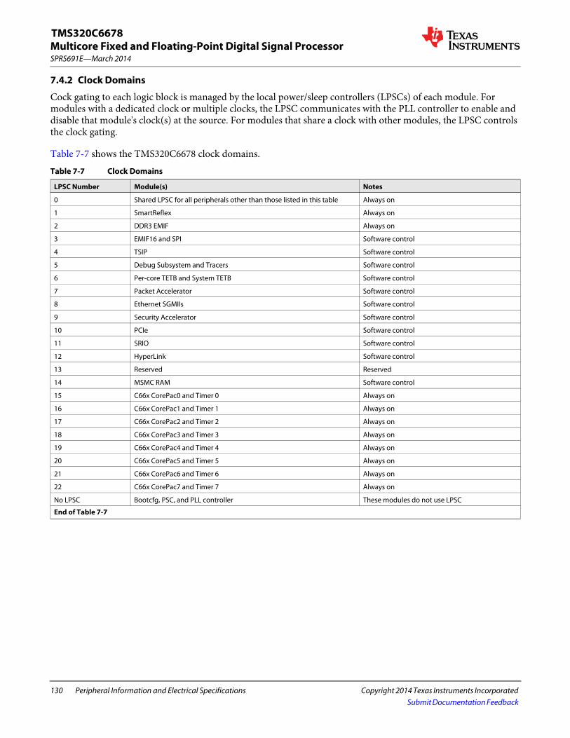
130 Peripheral Information and Electrical Specifications Copyright 2014 Texas Instruments Incorporated
SPRS691E—March 2014Multicore Fixed and Floating-Point Digital Signal ProcessorTMS320C6678
Submit Documentation Feedback
7.4.2 Clock Domains
Cock gating to each logic block is managed by the local power/sleep controllers (LPSCs) of each module. For modules with a dedicated clock or multiple clocks, the LPSC communicates with the PLL controller to enable and disable that module's clock(s) at the source. For modules that share a clock with other modules, the LPSC controls the clock gating.
Table 7-7 shows the TMS320C6678 clock domains. Table 7-7 Clock Domains
LPSC Number Module(s) Notes
0 Shared LPSC for all peripherals other than those listed in this table Always on
1 SmartReflex Always on
2 DDR3 EMIF Always on
3 EMIF16 and SPI Software control
4 TSIP Software control
5 Debug Subsystem and Tracers Software control
6 Per-core TETB and System TETB Software control
7 Packet Accelerator Software control
8 Ethernet SGMIIs Software control
9 Security Accelerator Software control
10 PCIe Software control
11 SRIO Software control
12 HyperLink Software control
13 Reserved Reserved
14 MSMC RAM Software control
15 C66x CorePac0 and Timer 0 Always on
16 C66x CorePac1 and Timer 1 Always on
17 C66x CorePac2 and Timer 2 Always on
18 C66x CorePac3 and Timer 3 Always on
19 C66x CorePac4 and Timer 4 Always on
20 C66x CorePac5 and Timer 5 Always on
21 C66x CorePac6 and Timer 6 Always on
22 C66x CorePac7 and Timer 7 Always on
No LPSC Bootcfg, PSC, and PLL controller These modules do not use LPSC
End of Table 7-7

Multicore Fixed and Floating-Point Digital Signal Processor
Copyright 2014 Texas Instruments Incorporated Peripheral Information and Electrical Specifications 131
SPRS691E—March 2014
TMS320C6678
Submit Documentation Feedback
7.4.3 PSC Register Memory Map
Table 7-8 shows the PSC Register memory map.Table 7-8 PSC Register Memory Map (Sheet 1 of 3)
Offset Register Description
0x000 PID Peripheral Identification Register
0x004 - 0x010 Reserved Reserved
0x014 VCNTLID Voltage Control Identification Register (1)
0x018 - 0x11C Reserved Reserved
0x120 PTCMD Power Domain Transition Command Register
0x124 Reserved Reserved
0x128 PTSTAT Power Domain Transition Status Register
0x12C - 0x1FC Reserved Reserved
0x200 PDSTAT0 Power Domain Status Register 0 (AlwaysOn)
0x204 PDSTAT1 Power Domain Status Register 1 (Per-core TETB and System TETB)
0x208 PDSTAT2 Power Domain Status Register 2 (Packet Coprocessor)
0x20C PDSTAT3 Power Domain Status Register 3 (PCIe)
0x210 PDSTAT4 Power Domain Status Register 4 (SRIO)
0x214 PDSTAT5 Power Domain Status Register 5 (HyperLink)
0x218 PDSTAT6 Power Domain Status Register 6 (Reserved)
0x21C PDSTAT7 Power Domain Status Register 7 (MSMC RAM)
0x220 PDSTAT8 Power Domain Status Register 8 (C66x CorePac0)
0x224 PDSTAT9 Power Domain Status Register 9 (C66x CorePac1)
0x228 PDSTAT10 Power Domain Status Register 10 (C66x CorePac2)
0x22C PDSTAT11 Power Domain Status Register 11 (C66x CorePac3)
0x230 PDSTAT12 Power Domain Status Register 12 (C66x CorePac4)
0x234 PDSTAT13 Power Domain Status Register 13 (C66x CorePac5)
0x238 PDSTAT14 Power Domain Status Register 14 (C66x CorePac6)
0x23C PDSTAT15 Power Domain Status Register 15 (C66x CorePac7)
0x240 - 0x2FC Reserved Reserved
0x300 PDCTL0 Power Domain Control Register 0 (AlwaysOn)
0x304 PDCTL1 Power Domain Control Register 1 (Per-core TETB and System TETB)
0x308 PDCTL2 Power Domain Control Register 2 (Packet Coprocessor)
0x30C PDCTL3 Power Domain Control Register 3 (PCIe)
0x310 PDCTL4 Power Domain Control Register 4 (SRIO)
0x314 PDCTL5 Power Domain Control Register 5 (HyperLink)
0x318 PDCTL6 Power Domain Control Register 6 (Reserved)
0x31C PDCTL7 Power Domain Control Register 7 (MSMC RAM)
0x320 PDCTL8 Power Domain Control Register 8 (C66x CorePac0)
0x324 PDCTL9 Power Domain Control Register 9 (C66x CorePac1)
0x328 PDCTL10 Power Domain Control Register 10 (C66x CorePac2)
0x32C PDCTL11 Power Domain Control Register 11 (C66x CorePac3)
0x330 PDCTL12 Power Domain Control Register 12 (C66x CorePac4)
0x334 PDCTL13 Power Domain Control Register 13 (C66x CorePac5)
0x338 PDCTL14 Power Domain Control Register 14 (C66x CorePac6)
0x33C PDCTL15 Power Domain Control Register 15 (C66x CorePac7)
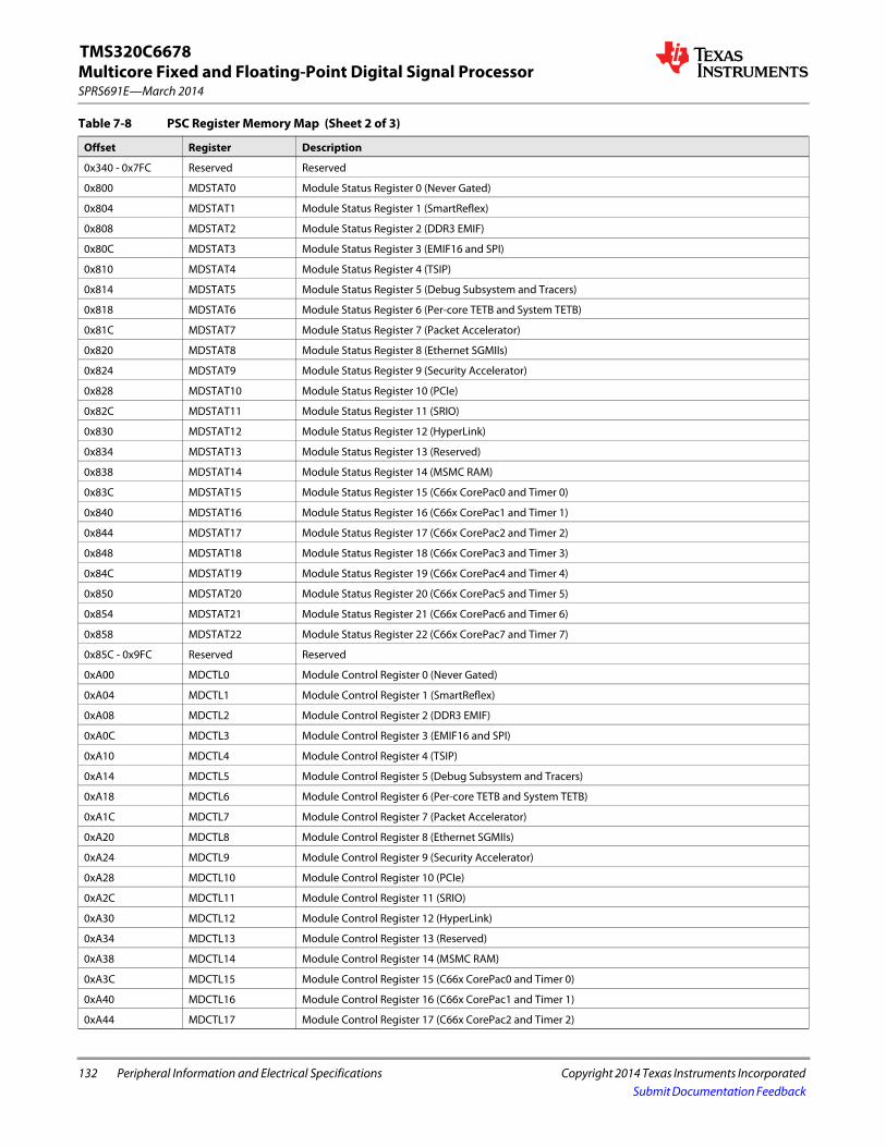
132 Peripheral Information and Electrical Specifications Copyright 2014 Texas Instruments Incorporated
SPRS691E—March 2014Multicore Fixed and Floating-Point Digital Signal ProcessorTMS320C6678
Submit Documentation Feedback
0x340 - 0x7FC Reserved Reserved
0x800 MDSTAT0 Module Status Register 0 (Never Gated)
0x804 MDSTAT1 Module Status Register 1 (SmartReflex)
0x808 MDSTAT2 Module Status Register 2 (DDR3 EMIF)
0x80C MDSTAT3 Module Status Register 3 (EMIF16 and SPI)
0x810 MDSTAT4 Module Status Register 4 (TSIP)
0x814 MDSTAT5 Module Status Register 5 (Debug Subsystem and Tracers)
0x818 MDSTAT6 Module Status Register 6 (Per-core TETB and System TETB)
0x81C MDSTAT7 Module Status Register 7 (Packet Accelerator)
0x820 MDSTAT8 Module Status Register 8 (Ethernet SGMIIs)
0x824 MDSTAT9 Module Status Register 9 (Security Accelerator)
0x828 MDSTAT10 Module Status Register 10 (PCIe)
0x82C MDSTAT11 Module Status Register 11 (SRIO)
0x830 MDSTAT12 Module Status Register 12 (HyperLink)
0x834 MDSTAT13 Module Status Register 13 (Reserved)
0x838 MDSTAT14 Module Status Register 14 (MSMC RAM)
0x83C MDSTAT15 Module Status Register 15 (C66x CorePac0 and Timer 0)
0x840 MDSTAT16 Module Status Register 16 (C66x CorePac1 and Timer 1)
0x844 MDSTAT17 Module Status Register 17 (C66x CorePac2 and Timer 2)
0x848 MDSTAT18 Module Status Register 18 (C66x CorePac3 and Timer 3)
0x84C MDSTAT19 Module Status Register 19 (C66x CorePac4 and Timer 4)
0x850 MDSTAT20 Module Status Register 20 (C66x CorePac5 and Timer 5)
0x854 MDSTAT21 Module Status Register 21 (C66x CorePac6 and Timer 6)
0x858 MDSTAT22 Module Status Register 22 (C66x CorePac7 and Timer 7)
0x85C - 0x9FC Reserved Reserved
0xA00 MDCTL0 Module Control Register 0 (Never Gated)
0xA04 MDCTL1 Module Control Register 1 (SmartReflex)
0xA08 MDCTL2 Module Control Register 2 (DDR3 EMIF)
0xA0C MDCTL3 Module Control Register 3 (EMIF16 and SPI)
0xA10 MDCTL4 Module Control Register 4 (TSIP)
0xA14 MDCTL5 Module Control Register 5 (Debug Subsystem and Tracers)
0xA18 MDCTL6 Module Control Register 6 (Per-core TETB and System TETB)
0xA1C MDCTL7 Module Control Register 7 (Packet Accelerator)
0xA20 MDCTL8 Module Control Register 8 (Ethernet SGMIIs)
0xA24 MDCTL9 Module Control Register 9 (Security Accelerator)
0xA28 MDCTL10 Module Control Register 10 (PCIe)
0xA2C MDCTL11 Module Control Register 11 (SRIO)
0xA30 MDCTL12 Module Control Register 12 (HyperLink)
0xA34 MDCTL13 Module Control Register 13 (Reserved)
0xA38 MDCTL14 Module Control Register 14 (MSMC RAM)
0xA3C MDCTL15 Module Control Register 15 (C66x CorePac0 and Timer 0)
0xA40 MDCTL16 Module Control Register 16 (C66x CorePac1 and Timer 1)
0xA44 MDCTL17 Module Control Register 17 (C66x CorePac2 and Timer 2)
Table 7-8 PSC Register Memory Map (Sheet 2 of 3)
Offset Register Description

Multicore Fixed and Floating-Point Digital Signal Processor
Copyright 2014 Texas Instruments Incorporated Peripheral Information and Electrical Specifications 133
SPRS691E—March 2014
TMS320C6678
Submit Documentation Feedback
7.5 Reset ControllerThe reset controller detects the different type of resets supported on the TMS320C6678 device and manages the distribution of those resets throughout the device.
The device has several types of resets: • Power-on reset• Hard reset• Soft reset• CPU local reset
Table 7-9 explains further the types of reset, the reset initiator, and the effects of each reset on the device. For more information on the effects of each reset on the PLL controllers and their clocks, see Section ‘‘Reset Electrical Data / Timing’’ on page 138
0xA48 MDCTL18 Module Control Register 18 (C66x CorePac3 and Timer 3)
0xA4C MDCTL19 Module Control Register 19 (C66x CorePac4 and Timer 4)
0xA50 MDCTL20 Module Control Register 20 (C66x CorePac5 and Timer 5)
0xA54 MDCTL21 Module Control Register 21 (C66x CorePac6 and Timer 6)
0xA58 MDCTL22 Module Control Register 22 (C66x CorePac7 and Timer 7)
0xA5C - 0xFFC Reserved Reserved
End of Table 7-8
1 VCNTLID register is available for debug purposes only.
Table 7-9 Reset Types
Reset Type Initiator Effect on Device When Reset Occurs RESETSTAT Pin Status
POR (Power On Reset) POR pin active low
RESETFULL pin active low
Total reset of the chip. Everything on the device is reset to its default state in response to this. Activates the POR signal on chip, which is used to reset test/emu logic. Boot configurations are latched. ROM boot process is initiated.
Toggles RESETSTAT pin
Hard Reset RESET pin active low
Emulation
PLLCTL register (RSCTRL)
Watchdog timers
Resets everything except for test/emu logic and reset isolation modules. Emulator and reset Isolation modules stay alive during this reset. This reset is also different from POR in that the PLLCTL assumes power and clocks are stable when device reset is asserted. Boot configurations are not latched. ROM boot process is initiated.
Toggles RESETSTAT pin
Soft Reset RESET pin active low
PLLCTL register (RSCTRL)
Watchdog timers
Software can program these initiators to be hard or soft. Hard reset is the default, but can be programmed to be soft reset. Soft reset will behave like hard reset except that EMIF16 MMRs, DDR3 EMIF MMRs, the sticky bits in PCIe MMRs, and external memory contents are retained. Boot configurations are not latched. ROM boot process is initiated.
Toggles RESETSTAT pin
C66x CorePac local reset
Software (through LPSC MMR)
Watchdog timersLRESET pin
MMR bit in LPSC controls C66x CorePac local reset. Used by watchdog timers (in the event of a timeout) to reset C66x CorePac. Can also be initiated by LRESET device pin. C66x CorePac memory system and slave DMA port are still alive when C66x CorePac is in local reset. Provides a local reset of the C66x CorePac, without destroying clock alignment or memory contents. Does not initiate ROM boot process.
Does not toggle RESETSTAT pin
End of Table 7-9
Table 7-8 PSC Register Memory Map (Sheet 3 of 3)
Offset Register Description

134 Peripheral Information and Electrical Specifications Copyright 2014 Texas Instruments Incorporated
SPRS691E—March 2014Multicore Fixed and Floating-Point Digital Signal ProcessorTMS320C6678
Submit Documentation Feedback
7.5.1 Power-on Reset
Power-on reset is used to reset the entire device, including the test and emulation logic.
Power-on reset is initiated by the following1. POR pin 2. RESETFULL pin
During power-up, the POR pin must be asserted (driven low) until the power supplies have reached their normal operating conditions. A RESETFULL pin is also provided to allow the on-board host to reset the entire device including the reset isolated logic. The assumption is that, device is already powered up and hence unlike POR, RESETFULL pin will be driven by the on-board host control other than the power good circuitry. For power-on reset, the Main PLL Controller comes up in bypass mode and the PLL is not enabled. Other resets do not affect the state of the PLL or the dividers in the PLL controller.
The following sequence must be followed during a power-on reset: 1. Wait for all power supplies to reach normal operating conditions while keeping the POR pin asserted (driven
low). While POR is asserted, all pins except RESETSTAT will be set to high-impedance. After the POR pin is de-asserted (driven high), all Z group pins, low group pins, and high group pins are set to their reset state and will remain at their reset state until otherwise configured by their respective peripheral. All peripherals that are power managed, are disabled after a Power-on Reset and must be enabled through the Device State Control registers (for more details, see Section Table 3-2 ‘‘Device State Control Registers’’ on page 74).
2. Clocks are reset, and they are propagated throughout the chip to reset any logic that was using reset synchronously. All logic is now reset and RESETSTAT will be driven low indicating that the device is in reset.
3. POR must be held active until all supplies on the board are stable then for at least an additional time for the Chip level PLLs to lock.
4. The POR pin can now be de-asserted. Reset sampled pin values are latched at this point. The Chip level PLLs is taken out of reset and begins its locking sequence, and all power-on device initialization also begins.
5. After device initialization is complete, the RESETSTAT pin is de-asserted (driven high). By this time, DDR3 PLL has already completed its locking sequence and is outputting a valid clock. The system clocks of both PLL controllers are allowed to finish their current cycles and then paused for 10 cycles of their respective system reference clocks. After the pause, the system clocks are restarted at their default divide by settings.
6. The device is now out of reset and device execution begins as dictated by the selected boot mode.
Note—To most of the device, reset is de-asserted only when the POR and RESET pins are both de-asserted (driven high). Therefore, in the sequence described above, if the RESET pin is held low past the low period of the POR pin, most of the device will remain in reset. The RESET pin should not be tied together with the POR pin.

Multicore Fixed and Floating-Point Digital Signal Processor
Copyright 2014 Texas Instruments Incorporated Peripheral Information and Electrical Specifications 135
SPRS691E—March 2014
TMS320C6678
Submit Documentation Feedback
7.5.2 Hard Reset
A hard reset will reset everything on the device except the PLLs, test, emulation logic, and reset isolation modules. POR should also remain de-asserted during this time.
Hard reset is initiated by the following• RESET pin• RSCTRL register in PLLCTL • Watchdog timer• Emulation
All the above initiators by default are configured to act as hard reset. Except emulation, all the other 3 initiators can be configured as soft resets in the RSCFG register in PLLCTL.
The following sequence must be followed during a hard reset: 1. The RESET pin is pulled active low for a minimum of 24 CLKIN1 cycles. During this time the RESET signal is
able to propagate to all modules (except those specifically mentioned above). All I/O are Hi-Z for modules affected by RESET, to prevent off-chip contention during the warm reset.
2. Once all logic is reset, RESETSTAT is driven active to denote that the device is in reset. 3. The RESET pin can now be released. A minimal device initialization begins to occur. Note that configuration
pins are not re-latched and clocking is unaffected within the device. 4. After device initialization is complete, the RESETSTAT pin is de-asserted (driven high).
Note—The POR pin should be held inactive (high) throughout the warm reset sequence. Otherwise, if POR is activated (brought low), the minimum POR pulse width must be met. The RESET pin should not be tied together with the POR pin.

136 Peripheral Information and Electrical Specifications Copyright 2014 Texas Instruments Incorporated
SPRS691E—March 2014Multicore Fixed and Floating-Point Digital Signal ProcessorTMS320C6678
Submit Documentation Feedback
7.5.3 Soft Reset
A soft reset will behave like a hard reset except that EMIF16 MMRs, DDR3 EMIF MMRs and the PCIe MMRs sticky bits, and external memory contents are retained. POR should also remain de-asserted during this time.
Soft reset is initiated by the following• RESET pin• RSCTRL register in PLLCTL • Watchdog timer
All the above initiators by default are configured to act as hard reset. Except emulation, all the other 3 initiators can be configured as soft resets in the RSCFG register in PLLCTL.
In the case of a soft reset, the clock logic or the power control logic of the peripherals are not affected, and, therefore, the enabled/disabled state of the peripherals is not affected. On a soft reset, the DDR3 memory controller registers are not reset. In addition, the DDR3 SDRAM memory content is retained if the user places the DDR3 SDRAM in self-refresh mode before invoking the soft reset.
During a soft reset, the following happens: 1. The RESETSTAT pin goes low to indicate an internal reset is being generated. The reset is allowed to propagate
through the system. Internal system clocks are not affected. PLLs also remain locked. 2. After device initialization is complete, the RESETSTAT pin is deasserted (driven high). In addition, the PLL
controllers pause their system clocks for about 8 cycles. At this point: › The state of the peripherals before the soft reset is not changed. › The I/O pins are controlled as dictated by the DEVSTAT register. › The DDR3 MMRs and the PCIe MMRs sticky bits retain their previous values. Only the DDR3
Memory Controller and PCIe state machines are reset by the soft reset. › The PLL controllers are operating in the mode prior to soft reset. System clocks are unaffected.
The boot sequence is started after the system clocks are restarted. Because the configuration pins are not latched with a System Reset, the previous values, as shown in the DEVSTAT register, are used to select the boot mode.

Multicore Fixed and Floating-Point Digital Signal Processor
Copyright 2014 Texas Instruments Incorporated Peripheral Information and Electrical Specifications 137
SPRS691E—March 2014
TMS320C6678
Submit Documentation Feedback
7.5.4 Local Reset
The local reset can be used to reset a particular CorePac without resetting any other chip components.
Local reset is initiated by the following (for more details see the Phase Locked Loop (PLL) for KeyStone Devices User Guide in ‘‘Related Documentation from Texas Instruments’’ on page 72:
• LRESET pin• Watchdog timer should cause one of the below based on the setting of the CORESEL[2:0] and RSTCFG
register in the PLL controller. See ‘‘Reset Configuration Register (RSTCFG)’’ on page 148 and ‘‘CIC Registers’’ on page 183:– Local reset– NMI– NMI followed by a time delay and then a local reset for the CorePac selected– Hard Reset by requesting reset via PLLCTL
• LPSC MMRs (memory-mapped registers)
7.5.5 Reset Priority
If any of the above reset sources occur simultaneously, the PLLCTL processes only the highest priority reset request. The reset request priorities are as follows (high to low):
• Power-on reset • Hard/soft reset
7.5.6 Reset Controller Register
The reset controller register are part of the PLLCTL MMRs. All C6678 device-specific MMRs are covered in Section 7.6.3 ‘‘Main PLL Control Register’’ on page 150. For more details on these registers and how to program them, see the Phase Locked Loop (PLL) for KeyStone Devices User Guide in ‘‘Related Documentation from Texas Instruments’’ on page 72.

138 Peripheral Information and Electrical Specifications Copyright 2014 Texas Instruments Incorporated
SPRS691E—March 2014Multicore Fixed and Floating-Point Digital Signal ProcessorTMS320C6678
Submit Documentation Feedback
7.5.7 Reset Electrical Data / Timing
Figure 7-6 RESETFULL Reset Timing
Figure 7-7 Soft/Hard-Reset Timing
Table 7-10 Reset Timing Requirements (1)
(see Figure 7-6 and Figure 7-7)
1 C = 1/SYSCLK1 frequency in ns.
No. Min Max Unit
RESETFULL Pin Reset
1 tw(RESETFULL) Pulse width - Pulse width RESETFULL low 500C ns
Soft/Hard-Reset
2 tw(RESET) Pulse width - Pulse width RESET low 500C ns
End of Table 7-10
Table 7-11 Reset Switching Characteristics Over Recommended Operating Conditions (1)
(see Figure 7-6 and Figure 7-7)
1 C = 1/SYSCLK1 frequency in ns.
No. Parameter Min Max Unit
RESETFULL Pin Reset
3 td(RESETFULLH-RESETSTATH) Delay time - RESETSTAT high after RESETFULL high 50000C ns
Soft/Hard Reset
4 td(RESETH-RESETSTATH) Delay time - RESETSTAT high after RESET high 50000C ns
End of Table 7-11
3
POR
RESET
RESETFULL
RESETSTAT
1
4
POR
RESET
RESETFULL
RESETSTAT
2

Multicore Fixed and Floating-Point Digital Signal Processor
Copyright 2014 Texas Instruments Incorporated Peripheral Information and Electrical Specifications 139
SPRS691E—March 2014
TMS320C6678
Submit Documentation Feedback
Figure 7-8 Boot Configuration Timing
Table 7-12 Boot Configuration Timing Requirements (1) (See Figure 7-8)
1 C = 1/SYSCLK1 frequency in ns.
No. Min Max Unit
1 tsu(GPIOn-RESETFULL) Setup time - GPIO valid before RESETFULL asserted 12C ns
2 th(RESETFULL-GPIOn) Hold time - GPIO valid after RESETFULL asserted 12C ns
End of Table 7-12
1
RESETFULL
GPIO[15:0]
2
POR

140 Peripheral Information and Electrical Specifications Copyright 2014 Texas Instruments Incorporated
SPRS691E—March 2014Multicore Fixed and Floating-Point Digital Signal ProcessorTMS320C6678
Submit Documentation Feedback
7.6 Main PLL and PLL ControllerThis section provides a description of the Main PLL and the PLL Controller. For details on the operation of the PLL Controller module, see the Phase Locked Loop (PLL) for KeyStone Devices User Guide in ‘‘Related Documentation from Texas Instruments’’ on page 72.
The Main PLL is controlled by the standard PLL Controller. The PLL controller manages the clock ratios, alignment, and gating for the system clocks to the device. Figure 7-9 shows a block diagram of the main PLL and the PLL Controller. Figure 7-9 Main PLL and PLL Controller
1
0
OUTPUTDIVIDE
CORECLK(N|P)
xPLLMPLLD
PLL
BYPASS
OUTPUTDIVIDE
PLLOUT
SYSCLK11/6
PLLDIV11
To Switch Fabric,Peripherals,Accelerators
PLL Controller
SYSCLK8/z
PLLDIV8
SYSCLK2/x
PLLDIV2
SYSCLK3/2
PLLDIV3
SYSCLK4/3
PLLDIV4
SYSCLK5/y
PLLDIV5
SYSCLK6/64
PLLDIV6
SYSCLK7/6
PLLDIV7
SYSCLK9/12
PLLDIV9
SYSCLK10/3
PLLDIV10
C66xCorePac
SYSCLK1/1PLLDIV1
1
0
1
0
0
PLLEN
PLLENSRC
Multicore Fixed and Floating-Point Digital Signal Processor
Copyright 2014 Texas Instruments Incorporated Peripheral Information and Electrical Specifications 141
SPRS691E—March 2014
TMS320C6678
Submit Documentation Feedback
Note—The Main PLL Controller registers can be accessed by any master in the device. The PLLM[5:0] bits of the multiplier are controlled by the PLLM register inside the PLL controller and PLLM[12:6] bits are controlled by the chip-level MAINPLLCTL0 register. The Output Divide and Bypass logic of the PLL are controlled by fields in the SECCTL register in the PLL controller. Only PLLDIV2, PLLDIV5, and PLLDIV8 are programmable on the C6678 device. See the Phase Locked Loop (PLL) for KeyStone Devices User Guide in ‘‘Related Documentation from Texas Instruments’’ on page 72 for more details on how to program the PLL controller.
The multiplication and division ratios within the PLL and the post-division for each of the chip-level clocks are determined by a combination of this PLL and the PLL Controller. The PLL controller also controls reset propagation through the chip, clock alignment, and test points. The PLL controller monitors the PLL status and provides an output signal indicating when the PLL is locked.
Main PLL power is supplied externally via the Main PLL power-supply pin (AVDDA1). An external EMI filter circuit must be added to all PLL supplies. See the Hardware Design Guide for KeyStone I Devices in ‘‘Related Documentation from Texas Instruments’’ on page 72 for detailed recommendations. For the best performance, TI recommends that all the PLL external components be on a single side of the board without jumpers, switches, or components other than those shown. For reduced PLL jitter, maximize the spacing between switching signal traces and the PLL external components (C1, C2, and the EMI Filter).
The minimum SYSCLK rise and fall times should also be observed. For the input clock timing requirements, see Section 7.6.5 ‘‘Main PLL Controller/SRIO/HyperLink/PCIe Clock Input Electrical Data/Timing’’.
Note—The PLL controller module as described in the see the Phase Locked Loop (PLL) for KeyStone Devices User Guide in ‘‘Related Documentation from Texas Instruments’’ on page 72 includes a superset of features, some of which are not supported on the TMS320C6678 device. The following sections describe the registers that are supported; it should be assumed that any registers not included in these sections is not supported by the device. Furthermore, only the bits within the registers described here are supported. Avoid writing to any reserved memory location or changing the value of reserved bits.
7.6.1 Main PLL Controller Device-Specific Information
7.6.1.1 Internal Clocks and Maximum Operating Frequencies
The Main PLL, used to drive the CorePacs, the switch fabric, and a majority of the peripheral clocks (all but the DDR3 and the network coprocessor (PASS)) requires a PLL controller to manage the various clock divisions, gating, and synchronization. The Main PLL Controller has several SYSCLK outputs that are listed below, along with the clock description. Each SYSCLK has a corresponding divider that divides down the output clock of the PLL. Note that dividers are not programmable unless explicitly mentioned in the description below.
• SYSCLK1: Full-rate clock for the CorePacs. • SYSCLK2: 1/x-rate clock for CorePac (emulation). Default rate for this is 1/3. This is programmable from /1
to /32, where this clock does not violate the max of 350 MHz. The SYSCLK2 can be turned off by software.• SYSCLK3: 1/2-rate clock used to clock the MSMC, HyperLink, CPU/2 TeraNet, DDR EMIF and CPU/2
EDMA.• SYSCLK4: 1/3-rate clock for the switch fabrics and fast peripherals. The Debug_SS and ETBs use this as well.• SYSCLK5: 1/y-rate clock for system trace module, only. Default rate for this is 1/5. It is configurable and the
max configurable clock is 210 MHz and min configuration clock is 32 MHz. The SYSCLK5 can be turned off by software.

142 Peripheral Information and Electrical Specifications Copyright 2014 Texas Instruments Incorporated
SPRS691E—March 2014Multicore Fixed and Floating-Point Digital Signal ProcessorTMS320C6678
Submit Documentation Feedback
• SYSCLK6: 1/64-rate clock. 1/64 rate clock (emif_ptv) used to clock the PVT compensated buffers for DDR3 EMIF.
• SYSCLK7: 1/6-rate clock for slow peripherals (GPIO, UART, Timer, I2C, SPI, EMIF16, etc.) and sources the SYSCLKOUT output pin.
• SYSCLK8: 1/z-rate clock. This clock is used as slow_sysclk in the system. Default for this will be 1/64. This is programmable from /24 to /80.
• SYSCLK9: 1/12-rate clock for SmartReflex.• SYSCLK10: 1/3-rate clock for SRIO only.• SYSCLK11: 1/6-rate clock for PSC only.
Only SYSCLK2, SYSCLK5, and SYSCLK8 are programmable on the TMS320C6678 device.
Note—In case any of the other programmable SYSCLKs are set slower than 1/64 rate, then SYSCLK8 (SLOW_SYSCLK) must be programmed to either match, or be slower than, the slowest SYSCLK in the system.
7.6.1.2 Main PLL Controller Operating Modes
The Main PLL Controller has two modes of operation: bypass mode and PLL mode. The mode of operation is determined by BYPASS bit of the PLL Secondary control register (SECCTL). In PLL mode, SYSCLK1 is generated from the PLL output using the values set in PLLM and PLLD bit fields in the MAINPLLCTL0 register. In bypass mode, PLL input is fed directly out as SYSCLK1.
All hosts must hold off accesses to the DSP while the frequency of its internal clocks is changing. A mechanism must be in place such that the DSP notifies the host when the PLL configuration has completed.
7.6.1.3 Main PLL Stabilization, Lock, and Reset Times
The PLL stabilization time is the amount of time that must be allotted for the internal PLL regulators to become stable after device powerup. The PLL should not be operated until this stabilization time has elapsed.
The PLL reset time is the amount of wait time needed when resetting the PLL (writing PLLRST = 1), in order for the PLL to properly reset, before bringing the PLL out of reset (writing PLLRST = 0). For the Main PLL reset time value, see Table 7-13.
The PLL lock time is the amount of time needed from when the PLL is taken out of reset (PLLRST = 1) to when to when the PLL Controller can be switched to PLL mode. The Main PLL lock time is given in Table 7-13.Table 7-13 Main PLL Stabilization, Lock, and Reset Times
Min Typ Max Unit
PLL stabilization time 100 μs
PLL lock time 500×(PLLD (1)+1)×C (2)
1 PLLD is the value in PLLD bit fields of MAINPLLCTL0 register2 C = SYSCLK1 cycle time in ns.
PLL reset time 1000 ns
End of Table 7-13
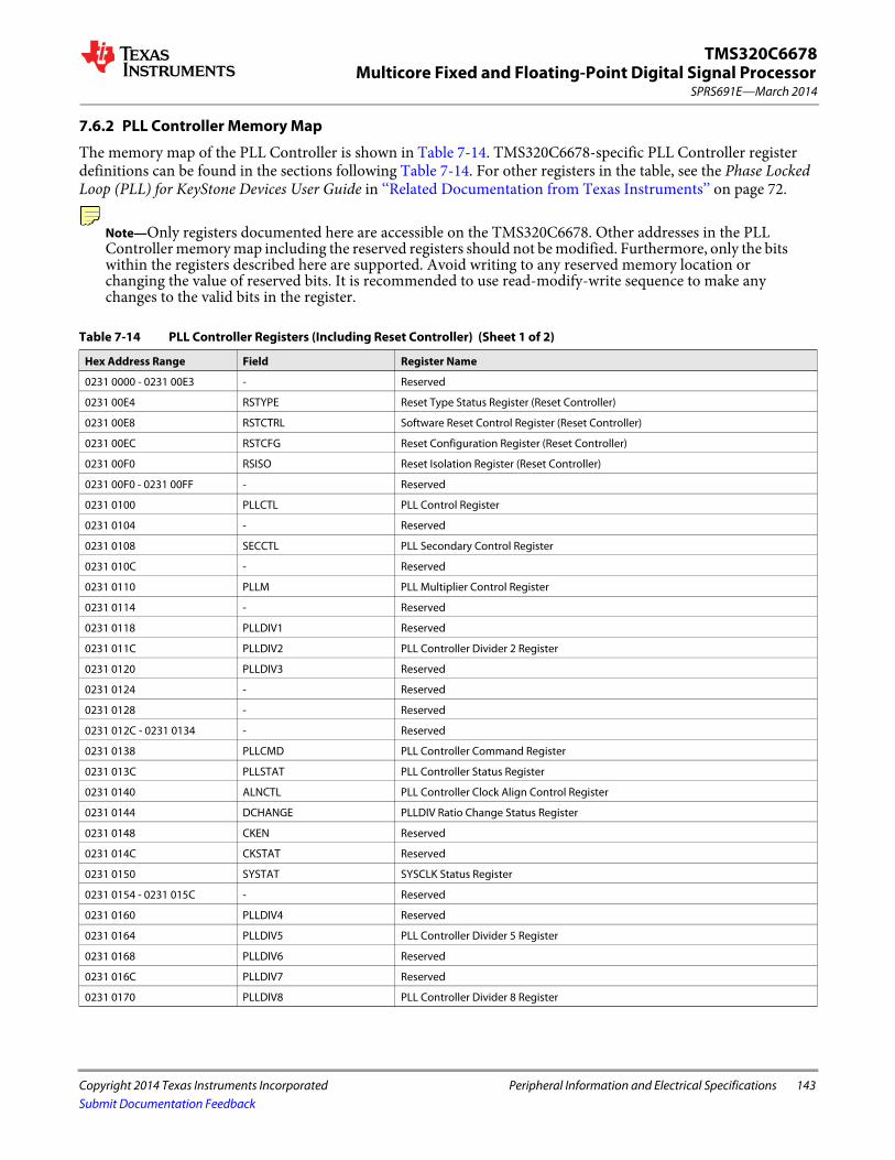
Multicore Fixed and Floating-Point Digital Signal Processor
Copyright 2014 Texas Instruments Incorporated Peripheral Information and Electrical Specifications 143
SPRS691E—March 2014
TMS320C6678
Submit Documentation Feedback
7.6.2 PLL Controller Memory Map
The memory map of the PLL Controller is shown in Table 7-14. TMS320C6678-specific PLL Controller register definitions can be found in the sections following Table 7-14. For other registers in the table, see the Phase Locked Loop (PLL) for KeyStone Devices User Guide in ‘‘Related Documentation from Texas Instruments’’ on page 72.
Note—Only registers documented here are accessible on the TMS320C6678. Other addresses in the PLL Controller memory map including the reserved registers should not be modified. Furthermore, only the bits within the registers described here are supported. Avoid writing to any reserved memory location or changing the value of reserved bits. It is recommended to use read-modify-write sequence to make any changes to the valid bits in the register.
Table 7-14 PLL Controller Registers (Including Reset Controller) (Sheet 1 of 2)
Hex Address Range Field Register Name
0231 0000 - 0231 00E3 - Reserved
0231 00E4 RSTYPE Reset Type Status Register (Reset Controller)
0231 00E8 RSTCTRL Software Reset Control Register (Reset Controller)
0231 00EC RSTCFG Reset Configuration Register (Reset Controller)
0231 00F0 RSISO Reset Isolation Register (Reset Controller)
0231 00F0 - 0231 00FF - Reserved
0231 0100 PLLCTL PLL Control Register
0231 0104 - Reserved
0231 0108 SECCTL PLL Secondary Control Register
0231 010C - Reserved
0231 0110 PLLM PLL Multiplier Control Register
0231 0114 - Reserved
0231 0118 PLLDIV1 Reserved
0231 011C PLLDIV2 PLL Controller Divider 2 Register
0231 0120 PLLDIV3 Reserved
0231 0124 - Reserved
0231 0128 - Reserved
0231 012C - 0231 0134 - Reserved
0231 0138 PLLCMD PLL Controller Command Register
0231 013C PLLSTAT PLL Controller Status Register
0231 0140 ALNCTL PLL Controller Clock Align Control Register
0231 0144 DCHANGE PLLDIV Ratio Change Status Register
0231 0148 CKEN Reserved
0231 014C CKSTAT Reserved
0231 0150 SYSTAT SYSCLK Status Register
0231 0154 - 0231 015C - Reserved
0231 0160 PLLDIV4 Reserved
0231 0164 PLLDIV5 PLL Controller Divider 5 Register
0231 0168 PLLDIV6 Reserved
0231 016C PLLDIV7 Reserved
0231 0170 PLLDIV8 PLL Controller Divider 8 Register
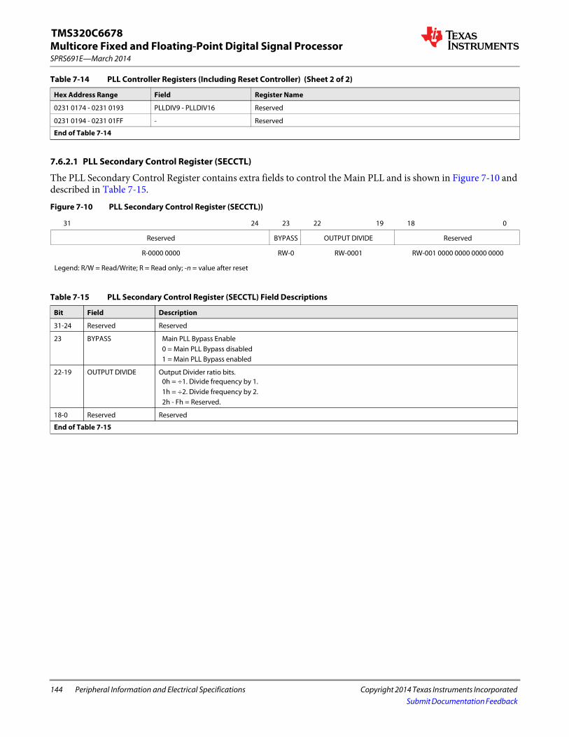
144 Peripheral Information and Electrical Specifications Copyright 2014 Texas Instruments Incorporated
SPRS691E—March 2014Multicore Fixed and Floating-Point Digital Signal ProcessorTMS320C6678
Submit Documentation Feedback
7.6.2.1 PLL Secondary Control Register (SECCTL)
The PLL Secondary Control Register contains extra fields to control the Main PLL and is shown in Figure 7-10 and described in Table 7-15.
0231 0174 - 0231 0193 PLLDIV9 - PLLDIV16 Reserved
0231 0194 - 0231 01FF - Reserved
End of Table 7-14
Figure 7-10 PLL Secondary Control Register (SECCTL))
31 24 23 22 19 18 0
Reserved BYPASS OUTPUT DIVIDE Reserved
R-0000 0000 RW-0 RW-0001 RW-001 0000 0000 0000 0000
Legend: R/W = Read/Write; R = Read only; -n = value after reset
Table 7-15 PLL Secondary Control Register (SECCTL) Field Descriptions
Bit Field Description
31-24 Reserved Reserved
23 BYPASS Main PLL Bypass Enable0 = Main PLL Bypass disabled1 = Main PLL Bypass enabled
22-19 OUTPUT DIVIDE Output Divider ratio bits. 0h = ÷1. Divide frequency by 1. 1h = ÷2. Divide frequency by 2. 2h - Fh = Reserved.
18-0 Reserved Reserved
End of Table 7-15
Table 7-14 PLL Controller Registers (Including Reset Controller) (Sheet 2 of 2)
Hex Address Range Field Register Name

Multicore Fixed and Floating-Point Digital Signal Processor
Copyright 2014 Texas Instruments Incorporated Peripheral Information and Electrical Specifications 145
SPRS691E—March 2014
TMS320C6678
Submit Documentation Feedback
7.6.2.2 PLL Controller Divider Register (PLLDIV2, PLLDIV5, PLLDIV8)
The PLL controller divider registers (PLLDIV2, PLLDIV5, and PLLDIV8) are shown in Figure 7-11 and described in Table 7-16. The default values of the RATIO field on a reset for PLLDIV2, PLLDIV5, and PLLDIV8 are different and mentioned in the footnote of Figure 7-11.
7.6.2.3 PLL Controller Clock Align Control Register (ALNCTL)
The PLL Controller clock align control register (ALNCTL) is shown in Figure 7-12 and described in Table 7-17.
Figure 7-11 PLL Controller Divider Register (PLLDIVn)
31 16 15 14 8 7 0
Reserved Dn (1) EN
1 D2EN for PLLDIV2; D5EN for PLLDIV5; D8EN for PLLDIV8
Reserved RATIO
R-0 R/W-1 R-0 R/W-n (2)
2 n=02h for PLLDIV2; n=04h for PLLDIV5; n=3Fh for PLLDIV8
Legend: R/W = Read/Write; R = Read only; -n = value after reset
Table 7-16 PLL Controller Divider Register (PLLDIVn) Field Descriptions
Bit Field Description
31-16 Reserved Reserved.
15 DnEN Divider Dn enable bit. (see footnote of Figure 7-11)0 = Divider n is disabled. 1 = No clock output. Divider n is enabled.
14-8 Reserved Reserved. The reserved bit location is always read as 0. A value written to this field has no effect.
7-0 RATIO Divider ratio bits. (see footnote of Figure 7-11)0h = ÷1. Divide frequency by 1. 1h = ÷2. Divide frequency by 2. 2h = ÷3. Divide frequency by 3. 3h = ÷4. Divide frequency by 4. 4h - 4Fh = ÷5 to ÷80. Divide frequency by 5 to divide frequency by 80.
End of Table 7-16
Figure 7-12 PLL Controller Clock Align Control Register (ALNCTL)
31 8 7 6 5 4 3 2 1 0
Reserved ALN8 Reserved ALN5 Reserved ALN2 Reserved
R-0 R/W-1 R-0 R/W-1 R-0 R/W-1 R-0
Legend: R/W = Read/Write; R = Read only; -n = value after reset, for reset value

146 Peripheral Information and Electrical Specifications Copyright 2014 Texas Instruments Incorporated
SPRS691E—March 2014Multicore Fixed and Floating-Point Digital Signal ProcessorTMS320C6678
Submit Documentation Feedback
7.6.2.4 PLLDIV Divider Ratio Change Status Register (DCHANGE)
Whenever a different ratio is written to the PLLDIVn registers, the PLLCTL flags the change in the DCHANGE status register. During the GO operation, the PLL Controller will change only the divide ratio of the SYSCLKs with the bit set in DCHANGE. Note that the ALNCTL register determines if that clock also needs to be aligned to other clocks. The PLLDIV divider ratio change status register is shown in Figure 7-13 and described in Table 7-18.
7.6.2.5 SYSCLK Status Register (SYSTAT)
The SYSCLK status register (SYSTAT) shows the status of SYSCLK[11:1]. SYSTAT is shown in Figure 7-14 and described in Table 7-19.
Table 7-17 PLL Controller Clock Align Control Register (ALNCTL) Field Descriptions
Bit Field Description
31-8
6-5
3-2
0
Reserved Reserved. The reserved bit location is always read as 0. A value written to this field has no effect.
7
4
1
ALN8
ALN5
ALN2
SYSCLKn alignment. Do not change the default values of these fields. 0 = Do not align SYSCLKn to other SYSCLKs during GO operation. If SYSn in DCHANGE is set, SYSCLKn switches to the new
ratio immediately after the GOSET bit in PLLCMD is set. 1 = Align SYSCLKn to other SYSCLKs selected in ALNCTL when the GOSET bit in PLLCMD is set and SYSn in DCHANGE is 1.
The SYSCLKn rate is set to the ratio programmed in the RATIO bit in PLLDIVn.
End of Table 7-17
Figure 7-13 PLLDIV Divider Ratio Change Status Register (DCHANGE)
31 8 7 6 5 4 3 2 1 0
Reserved SYS8 Reserved SYS5 Reserved SYS2 Reserved
R-0 R/W-0 R-0 R/W-0 R-0 R/W-0 R-0
Legend: R/W = Read/Write; R = Read only; -n = value after reset, for reset value
Table 7-18 PLLDIV Divider Ratio Change Status Register (DCHANGE) Field Descriptions
Bit Field Description
31-8
6-5
3-2
0
Reserved Reserved. The reserved bit location is always read as 0. A value written to this field has no effect.
7
4
1
SYS8
SYS5
SYS2
Identifies when the SYSCLKn divide ratio has been modified. 0 = SYSCLKn ratio has not been modified. When GOSET is set, SYSCLKn will not be affected. 1 = SYSCLKn ratio has been modified. When GOSET is set, SYSCLKn will change to the new ratio.
End of Table 7-18
Figure 7-14 SYSCLK Status Register (SYSTAT)
31 11 10 9 8 7 6 5 4 3 2 1 0
Reserved SYS11ON SYS10ON SYS9ON SYS8ON SYS7ON SYS6ON SYS5ON SYS4ON SYS3ON SYS2ON SYS1ON
R-n R-1 R-1 R-1 R-1 R-1 R-1 R-1 R-1 R-1 R-1 R-1
Legend: R/W = Read/Write; R = Read only; -n = value after reset

Multicore Fixed and Floating-Point Digital Signal Processor
Copyright 2014 Texas Instruments Incorporated Peripheral Information and Electrical Specifications 147
SPRS691E—March 2014
TMS320C6678
Submit Documentation Feedback
7.6.2.6 Reset Type Status Register (RSTYPE)
The reset type status (RSTYPE) register latches the cause of the last reset. If multiple reset sources occur simultaneously, this register latches the highest priority reset source. The Reset Type Status Register is shown in Figure 7-15 and described in Table 7-20.
Table 7-19 SYSCLK Status Register (SYSTAT) Field Descriptions
Bit Field Description
31-11 Reserved Reserved. The reserved bit location is always read as 0. A value written to this field has no effect.
10-0 SYS[N (1)]ON
1 Where N = 1, 2, 3,....N (Not all these output clocks may be used on a specific device. For more information, see the device-specific data manual)
SYSCLK[N] on status. 0 = SYSCLK[N] is gated. 1 = SYSCLK[N] is on.
End of Table 7-19
Figure 7-15 Reset Type Status Register (RSTYPE)
31 29 28 27 12 11 8 7 3 2 1 0
Reserved EMU-RST Reserved WDRST[N] Reserved PLLCTRLRST RESET POR
R-0 R-0 R-0 R-0 R-0 R-0 R-0 R-0
Legend: R = Read only; -n = value after reset
Table 7-20 Reset Type Status Register (RSTYPE) Field Descriptions
Bit Field Description
31-29 Reserved Reserved. Read only. Always reads as 0. Writes have no effect.
28 EMU-RST Reset initiated by emulation.0 = Not the last reset to occur.1 = The last reset to occur.
27-12 Reserved Reserved. Read only. Always reads as 0. Writes have no effect.
11
10
9
8
WDRST3
WDRST2
WDRST1
WDRST0
Reset initiated by watchdog timer[N].0 = Not the last reset to occur.1 = The last reset to occur.
7-3 Reserved Reserved. Read only. Always reads as 0. Writes have no effect.
2 PLLCTLRST Reset initiated by PLLCTL.0 = Not the last reset to occur.1 = The last reset to occur.
1 RESET RESET reset.0 = RESET was not the last reset to occur.1 = RESET was the last reset to occur.
0 POR Power-on reset.0 = Power-on reset was not the last reset to occur.1 = Power-on reset was the last reset to occur.
End of Table 7-20

148 Peripheral Information and Electrical Specifications Copyright 2014 Texas Instruments Incorporated
SPRS691E—March 2014Multicore Fixed and Floating-Point Digital Signal ProcessorTMS320C6678
Submit Documentation Feedback
7.6.2.7 Reset Control Register (RSTCTRL)
This register contains a key that enables writes to the MSB of this register and the RSTCFG register. The key value is 0x5A69. A valid key will be stored as 0x000C, any other key value is invalid. When the RSTCTRL or the RSTCFG is written, the key is invalidated. Every write must be set up with a valid key. The Software Reset Control Register (RSTCTRL) is shown in Figure 7-16 and described in Table 7-21.
7.6.2.8 Reset Configuration Register (RSTCFG)
This register is used to configure the type of reset initiated by RESET, watchdog timer and the PLL Controller’s RSTCTRL Register; i.e., a hard reset or a soft reset. By default, these resets will be hard resets. The Reset Configuration Register (RSTCFG) is shown in Figure 7-17 and described in Table 7-22.
Figure 7-16 Reset Control Register (RSTCTRL)
31 17 16 15 0
Reserved SWRST KEY
R-0x0000 R/W-0x (1)
1 Writes are conditional based on valid key.
R/W-0x0003
Legend: R = Read only; -n = value after reset;
Table 7-21 Reset Control Register (RSTCTRL) Field Descriptions
Bit Field Description
31-17 Reserved Reserved.
16 SWRST Software reset0 = Reset1 = Not reset
15-0 KEY Key used to enable writes to RSTCTRL and RSTCFG.
End of Table 7-21
Figure 7-17 Reset Configuration Register (RSTCFG)
31 14 13 12 11 4 3 0
Reserved PLLCTLRSTTYPE RESETTYPE Reserved WDTYPE[N (1)]
1 Where N = 1, 2, 3,....N (Not all these output may be used on a specific device. For more information, see the device-specific data manual)
R-0 R/W-0 (2)
2 Writes are conditional based on valid key. For details, see Section 7.6.2.7 ‘‘Reset Control Register (RSTCTRL)’’.
R/W-02 R-0 R/W-02
Legend: R = Read only; R/W = Read/Write; -n = value after reset
Table 7-22 Reset Configuration Register (RSTCFG) Field Descriptions (Sheet 1 of 2)
Bit Field Description
31-14 Reserved Reserved.
13 PLLCTLRSTTYPE PLL Controller initiates a software-driven reset of type:0 = Hard reset (default)1 = Soft reset
12 RESETTYPE RESET initiates a reset of type:0 = Hard reset (default)1 = Soft reset

Multicore Fixed and Floating-Point Digital Signal Processor
Copyright 2014 Texas Instruments Incorporated Peripheral Information and Electrical Specifications 149
SPRS691E—March 2014
TMS320C6678
Submit Documentation Feedback
7.6.2.9 Reset Isolation Register (RSISO)
This register is used to select the module clocks that must maintain their clocking without pausing through non power-on reset. Setting any of these bits effectively blocks reset to all PLLCTL registers in order to maintain current values of PLL multiplier, divide ratios and other settings. Along with setting module specific bit in RSISO, the corresponding MDCTLx[12] bit also must be set in PSC to reset isolate a particular module. For more information on MDCTLx register see the Power Sleep Controller (PSC) for KeyStone Devices User Guide in ‘‘Related Documentation from Texas Instruments’’ on page 72. The Reset Isolation Register (RSTCTRL) is shown in Figure 7-18 and described in Table 7-23.
Note—The boot ROM code will enable the reset isolation for both SRIO and SmartReflex modules during boot with the Reset Isolation Register. It is up to the user application to disable.
11-4 Reserved Reserved.
3
2
1
0
WDTYPE3
WDTYPE2
WDTYPE1
WDTYPE0
Watchdog timer [N] initiates a reset of type:0 = Hard reset (default)1 = Soft reset
End of Table 7-22
Figure 7-18 Reset Isolation Register (RSISO)
31 10 9 8 7 0
Reserved SRIOISO SRISO Reserved
R-0 R/W-0 R/W-0 R-0
Legend: R = Read only; R/W = Read/Write; -n = value after reset
Table 7-23 Reset Isolation Register (RSISO) Field Descriptions
Bit Field Description
31-10 Reserved Reserved.
9 SRIOISO Isolate SRIO module0 = Not reset isolated1 = Reset Isolated
8 SRISO Isolate SmartReflex0 = Not reset isolated1 = Reset Isolated
7-0 Reserved Reserved.
End of Table 7-23
Table 7-22 Reset Configuration Register (RSTCFG) Field Descriptions (Sheet 2 of 2)
Bit Field Description

150 Peripheral Information and Electrical Specifications Copyright 2014 Texas Instruments Incorporated
SPRS691E—March 2014Multicore Fixed and Floating-Point Digital Signal ProcessorTMS320C6678
Submit Documentation Feedback
7.6.3 Main PLL Control Register
The Main PLL uses two chip-level registers (MAINPLLCTL0 and MAINPLLCTL1) along with the PLL Controller for its configuration. These MMRs exist inside the Bootcfg space. To write to these registers, software should go through an un-locking sequence using KICK0/KICK1 registers. For valid configurable values into the MAINPLLCTL0 and MAINPLLCTL1 registers see Section 2.5.4 ‘‘PLL Boot Configuration Settings’’ on page 38. See section 3.3.4 ‘‘Kicker Mechanism Register (KICK0 and KICK1)’’ on page 80 for the address location of the registers and locking and unlocking sequences for accessing the registers. The registers are reset on POR only. Figure 7-19 Main PLL Control Register 0 (MAINPLLCTL0)
31 24 23 19 18 12 11 6 5 0
BWADJ[7:0] Reserved PLLM[12:6] Reserved PLLD
RW-0000 0101 RW-0000 0 RW-0000000 RW-000000 RW-000000
Legend: RW = Read/Write; -n = value after reset
Table 7-24 Main PLL Control Register 0 (MAINPLLCTL0) Field Descriptions
Bit Field Description
31-24 BWADJ[7:0] BWADJ[11:8] and BWADJ[7:0] are located in MAINPLLCTL0 and MAINPLLCTL1 registers. The combination (BWADJ[11:0]) should be programmed to a value related to PLLM[12:0] value based on the equation: BWADJ = ((PLLM+1)>>1) - 1
23-19 Reserved Reserved
18-12 PLLM[12:6] A 13-bit bus that selects the values for the multiplication factor (see Note— below)
11-6 Reserved Reserved
5-0 PLLD A 6-bit bus that selects the values for the reference divider
End of Table 7-24
Figure 7-20 Main PLL Control Register 1 (MAINPLLCTL1)
31 7 6 5 4 3 0
Reserved ENSAT Reserved BWADJ[11:8]
RW-0000000000000000000000000 RW-0 RW-00 RW-0000
Legend: RW = Read/Write; -n = value after reset
Table 7-25 Main PLL Control Register 1 (MAINPLLCTL1) Field Descriptions
Bit Field Description
31-7 Reserved Reserved
6 ENSAT Must be set to 1 for proper operation of PLL
5-4 Reserved Reserved
3-0 BWADJ[11:8] BWADJ[11:8] and BWADJ[7:0] are located in MAINPLLCTL0 and MAINPLLCTL1 registers. The combination (BWADJ[11:0]) should be programmed to a value related to PLLM[12:0] value based on the equation: BWADJ = ((PLLM+1)>>1) - 1
End of Table 7-25

Multicore Fixed and Floating-Point Digital Signal Processor
Copyright 2014 Texas Instruments Incorporated Peripheral Information and Electrical Specifications 151
SPRS691E—March 2014
TMS320C6678
Submit Documentation Feedback
Note—PLLM[5:0] bits of the multiplier is controlled by the PLLM register inside the PLL Controller and PLLM[12:6] bits are controlled by the MAINPLLCTL0 chip-level register. The MAINPLLCTL0 register PLLM[12:6] bits should be written just before writing to the PLLM register PLLM[5:0] bits in the controller to have the complete 13 bit value latched when the GO operation is initiated in the PLL controller. See the Phase Locked Loop (PLL) for KeyStone Devices User Guide in ‘‘Related Documentation from Texas Instruments’’ on page 72 for the recommended programming sequence. Output divide ratio and Bypass enable/disable of the Main PLL is controlled by the SECCTL register in the PLL Controller. See the 7.6.2.1 ‘‘PLL Secondary Control Register (SECCTL)’’ for more details.
7.6.4 Main PLL and PLL Controller Initialization Sequence
See the Phase Locked Loop (PLL) for KeyStone Devices User Guide in ‘‘Related Documentation from Texas Instruments’’ on page 72 for details on the initialization sequence for Main PLL and PLL Controller.
7.6.5 Main PLL Controller/SRIO/HyperLink/PCIe Clock Input Electrical Data/Timing
Table 7-26 Main PLL Controller/SRIO/HyperLink/PCIe Clock Input Timing Requirements (1) (Sheet 1 of 2)(see Figure 7-21 and Figure 7-22)
No. Min Max Unit
CORECLK[P:N]
1 tc(CORCLKN) Cycle time _ CORECLKN cycle time 3.2 25 ns
1 tc(CORECLKP) Cycle time _ CORECLKP cycle time 3.2 25 ns
3 tw(CORECLKN) Pulse width _ CORECLKN high 0.45*tc(CORECLKN) 0.55*tc(CORECLKN) ns
2 tw(CORECLKN) Pulse width _ CORECLKN low 0.45*tc(CORECLKN) 0.55*tc(CORECLKN) ns
2 tw(CORECLKP) Pulse width _ CORECLKP high 0.45*tc(CORECLKP) 0.55*tc(CORECLKP) ns
3 tw(CORECLKP) Pulse width _ CORECLKP low 0.45*tc(CORECLKP) 0.55*tc(CORECLKP) ns
4 tr(CORECLK_250mv) Transition time _ CORECLK differential rise time (250mV) 50 350 ps
4 tf(CORECLK_250mv) Transition time _ CORECLK differential fall time (250mV) 50 350 ps
5 tj(CORECLKN) Jitter, peak_to_peak _ periodic CORECLKN 0.02*tc(CORECLKN) ps
5 tj(CORECLKP) Jitter, peak_to_peak _ periodic CORECLKP 0.02*tc(CORECLKP) ps
SRIOSGMIICLK[P:N]
1 tc(SRIOSGMIICLKN) Cycle time _ SRIOSGMIICLKN cycle time 3.2 or 4 or 6.4 ns
1 tc(SRIOSGMIICLKP) Cycle time _ SRIOSGMIICLKP cycle time 3.2 or 4 or 6.4 ns
3 tw(SRIOSGMIICLKN) Pulse width _ SRIOSGMIICLKN high 0.45*tc(SRIOSGMIICLKN) 0.55*tc(SRIOSGMIICLKN) ns
2 tw(SRIOSGMIICLKN) Pulse width _ SRIOSGMIICLKN low 0.45*tc(SRIOSGMIICLKN) 0.55*tc(SRIOSGMIICLKN) ns
2 tw(SRIOSGMIICLKP) Pulse width _ SRIOSGMIICLKP high 0.45*tc(SRIOSGMIICLKP) 0.55*tc(SRIOSGMIICLKP) ns
3 tw(SRIOSGMIICLKP) Pulse width _ SRIOSGMIICLKP low 0.45*tc(SRIOSGMIICLKP) 0.55*tc(SRIOSGMIICLKP) ns
4 tr(SRIOSGMIICLK_250mv)
Transition time _ SRIOSGMIICLK differential rise time (250 mV) 50 350 ps
4 tf(SRIOSGMIICLK_250mv)
Transition time _ SRIOSGMIICLK differential fall time (250 mV) 50 350 ps
5 tj(SRIOSGMIICLKN) Jitter, peak_to_peak _ periodic SRIOSGMIICLKN 4 (2) ps,RMS
5 tj(SRIOSGMIICLKP) Jitter, peak_to_peak _ periodic SRIOSGMIICLKP 4 (2) ps,RMS
5 tj(SRIOSGMIICLKN) Jitter, peak_to_peak _ periodic SRIOSGMIICLKN (SRIO not used) 8 (2) ps,RMS
5 tj(SRIOSGMIICLKP) Jitter, peak_to_peak _ periodic SRIOSGMIICLKP (SRIO not used) 8 (2) ps,RMS

152 Peripheral Information and Electrical Specifications Copyright 2014 Texas Instruments Incorporated
SPRS691E—March 2014Multicore Fixed and Floating-Point Digital Signal ProcessorTMS320C6678
Submit Documentation Feedback
Figure 7-21 Main PLL Controller/SRIO/HyperLink/PCIe Clock Input Timing
Figure 7-22 Main PLL Clock Input Transition Time
HyperLinkCLK[P:N]
1 tc(MCMCLKN) Cycle time _ MCMCLKN cycle time 3.2 or 4 or 6.4 ns
1 tc(MCMCLKP) Cycle time _ MCMCLKP cycle time 3.2 or 4 or 6.4 ns
3 tw(MCMCLKN) Pulse width _ MCMCLKN high 0.45*tc(MCMCLKN) 0.55*tc(MCMCLKN) ns
2 tw(MCMCLKN) Pulse width _ MCMCLKN low 0.45*tc(MCMCLKN) 0.55*tc(MCMCLKN) ns
2 tw(MCMCLKP) Pulse width _ MCMCLKP high 0.45*tc(MCMCLKP) 0.55*tc(MCMCLKP) ns
3 tw(MCMCLKP) Pulse width _ MCMCLKP low 0.45*tc(MCMCLKP) 0.55*tc(MCMCLKP) ns
4 tr(MCMCLK_250mv) Transition time _ MCMCLK differential rise time (250mV) 50 350 ps
4 tf(MCMCLK_250mv) Transition time _ MCMCLK differential fall time (250mV) 50 350 ps
5 tj(MCMCLKN) Jitter, peak_to_peak _ periodic MCMCLKN 4 (2) ps,RMS
5 tj(MCMCLKP) Jitter, peak_to_peak _ periodic MCMCLKP 4 (2) ps,RMS
PCIECLK[P:N]
1 tc(PCIECLKN) Cycle time _ PCIECLKN cycle time 3.2 or 4 or 6.4 or 10 ns
1 tc(PCIECLKP) Cycle time _ PCIECLKP cycle time 3.2 or 4 or 6.4 or 10 ns
3 tw(PCIECLKN) Pulse width _ PCIECLKN high 0.45*tc(PCIECLKN) 0.55*tc(PCIECLKN) ns
2 tw(PCIECLKN) Pulse width _ PCIECLKN low 0.45*tc(PCIECLKN) 0.55*tc(PCIECLKN) ns
2 tw(PCIECLKP) Pulse width _ PCIECLKP high 0.45*tc(PCIECLKP) 0.55*tc(PCIECLKP) ns
3 tw(PCIECLKP) Pulse width _ PCIECLKP low 0.45*tc(PCIECLKP) 0.55*tc(PCIECLKP) ns
4 tr(PCIECLK_250mv) Transition time _ PCIECLK differential rise time (250 mV) 50 350 ps
4 tf(PCIECLK_250mv) Transition time _ PCIECLK differential fall time (250 mV) 50 350 ps
5 tj(PCIECLKN) Jitter, peak_to_peak _ periodic PCIECLKN 4 (2) ps,RMS
5 tj(PCIECLKP) Jitter, peak_to_peak _ periodic PCIECLKP 4 (2) ps,RMS
End of Table 7-26
1 See the Hardware Design Guide for KeyStone I Devices in ‘‘Related Documentation from Texas Instruments’’ on page 72 for detailed recommendations.2 The jitter frequency mask shown in the Hardware Design Guide for KeyStone Devices in ‘‘Related Documentation from Texas Instruments’’ on page 72 must also be met for
the specific operating mode chosen.
Table 7-26 Main PLL Controller/SRIO/HyperLink/PCIe Clock Input Timing Requirements (1) (Sheet 2 of 2)(see Figure 7-21 and Figure 7-22)
No. Min Max Unit
4
32
1
5
<CLK_NAME>CLKN
<CLK_NAME>CLKP
peak-to-peak Differential InputVoltage (250 mV to 2 V)
200 mV Transition Voltage Range0
T = 50 ps Min to 350 ps Max
for the 200-mVR
Transition Voltage Range
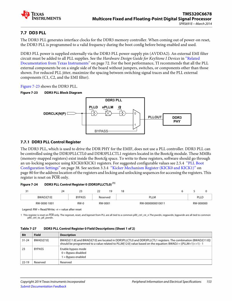
Multicore Fixed and Floating-Point Digital Signal Processor
Copyright 2014 Texas Instruments Incorporated Peripheral Information and Electrical Specifications 153
SPRS691E—March 2014
TMS320C6678
Submit Documentation Feedback
7.7 DD3 PLLThe DDR3 PLL generates interface clocks for the DDR3 memory controller. When coming out of power-on reset, the DDR3 PLL is programmed to a valid frequency during the boot config before being enabled and used.
DDR3 PLL power is supplied externally via the DDR3 PLL power-supply pin (AVDDA2). An external EMI filter circuit must be added to all PLL supplies. See the Hardware Design Guide for KeyStone I Devices in ‘‘Related Documentation from Texas Instruments’’ on page 72. For the best performance, TI recommends that all the PLL external components be on a single side of the board without jumpers, switches, or components other than those shown. For reduced PLL jitter, maximize the spacing between switching signal traces and the PLL external components (C1, C2, and the EMI filter).
Figure 7-23 shows the DDR3 PLL.Figure 7-23 DDR3 PLL Block Diagram
7.7.1 DDR3 PLL Control Register
The DDR3 PLL, which is used to drive the DDR PHY for the EMIF, does not use a PLL controller. DDR3 PLL can be controlled using the DDR3PLLCTL0 and DDR3PLLCTL1 registers located in the Bootcfg module. These MMRs (memory-mapped registers) exist inside the Bootcfg space. To write to these registers, software should go through an un-locking sequence using KICK0/KICK1 registers. For suggested configurable values see 2.5.4 ‘‘PLL Boot Configuration Settings’’ on page 38. See section 3.3.4 ‘‘Kicker Mechanism Register (KICK0 and KICK1)’’ on page 80 for the address location of the registers and locking and unlocking sequences for accessing the registers. This register is reset on POR only..Figure 7-24 DDR3 PLL Control Register 0 (DDR3PLLCTL0) (1)
1 This register is reset on POR only. The regreset, reset, and bgreset from PLL are all tied to a common pll0_ctrl_rst_n The pwrdn, regpwrdn, bgpwrdn are all tied to common pll0_ctrl_to_pll_pwrdn.
31 24 23 22 19 18 6 5 0
BWADJ[7:0] BYPASS Reserved PLLM PLLD
RW-0000 1001 RW-0 RW-0001 RW-0000000010011 RW-000000
Legend: RW = Read/Write; -n = value after reset
Table 7-27 DDR3 PLL Control Register 0 Field Descriptions (Sheet 1 of 2)
Bit Field Description
31-24 BWADJ[7:0] BWADJ[11:8] and BWADJ[7:0] are located in DDR3PLLCTL0 and DDR3PLLCTL1 registers. The combination (BWADJ[11:0]) should be programmed to a value related to PLLM[12:0] value based on the equation: BWADJ = ((PLLM+1)>>1) - 1
23 BYPASS Enable bypass mode0 = Bypass disabled1 = Bypass enabled
22-19 Reserved Reserved
DDR3PHY
DDRCLK(N|P)
1
0
/2xPLLMPLLD
BYPASS
/2
PLLOUT
DDR3 PLL

154 Peripheral Information and Electrical Specifications Copyright 2014 Texas Instruments Incorporated
SPRS691E—March 2014Multicore Fixed and Floating-Point Digital Signal ProcessorTMS320C6678
Submit Documentation Feedback
7.7.2 DDR3 PLL Device-Specific Information
As shown in Figure 7-23, the output of DDR3 PLL (PLLOUT) is divided by 2 and directly fed to the DDR3 memory controller. The DDR3 PLL is affected by power-on reset. During power-on resets, the internal clocks of the DDR3 PLL are affected as described in Section 7.5 ‘‘Reset Controller’’ on page 133. DDR3 PLL is unlocked only during the power-up sequence and is locked by the time the RESETSTAT pin goes high. It does not lose lock during any of the other resets.
7.7.3 DDR3 PLL Initialization Sequence
See the Phase Locked Loop (PLL) for KeyStone Devices User Guide in ‘‘Related Documentation from Texas Instruments’’ on page 72 for details on the initialization sequence for DDR3 PLL.
Note—The DDR3 interface must reset every time the DDR3 PLL is re-programmed.
18-6 PLLM A 13-bit bus that selects the values for the multiplication factor
5-0 PLLD A 6-bit bus that selects the values for the reference divider
End of Table 7-27
Figure 7-25 DDR3 PLL Control Register 1 (DDR3PLLCTL1)
31 14 13 12 7 6 5 4 3 0
Reserved PLLRST Reserved ENSAT Reserved BWADJ[11:8]
RW-000000000000000000 RW-0 RW-000000 RW-0 R-0 RW-0000
Legend: RW = Read/Write; -n = value after reset
Table 7-28 DDR3 PLL Control Register 1 Field Descriptions
Bit Field Description
31-14 Reserved Reserved
13 PLLRST PLL reset bit.0 = PLL reset is released.1 = PLL reset is asserted.
12-7 Reserved Reserved
6 ENSAT Must be set to 1 for proper operation of PLL
5-4 Reserved Reserved
3-0 BWADJ[11:8] BWADJ[11:8] and BWADJ[7:0] are located in DDR3PLLCTL0 and DDR3PLLCTL1 registers. The combination (BWADJ[11:0]) should be programmed to a value related to PLLM[12:0] value based on the equation: BWADJ = ((PLLM+1)>>1) - 1
End of Table 7-28
Table 7-27 DDR3 PLL Control Register 0 Field Descriptions (Sheet 2 of 2)
Bit Field Description

Multicore Fixed and Floating-Point Digital Signal Processor
Copyright 2014 Texas Instruments Incorporated Peripheral Information and Electrical Specifications 155
SPRS691E—March 2014
TMS320C6678
Submit Documentation Feedback
7.7.4 DDR3 PLL Input Clock Electrical Data/Timing
Figure 7-26 DDR3 PLL DDRCLK Timing
Table 7-29 DDR3 PLL DDRSYSCLK1(N|P) Timing Requirements (see Figure 7-26 and Figure 7-22)
No. Min Max Unit
DDRCLK[P:N]
1 tc(DDRCLKN) Cycle time _ DDRCLKN cycle time 3.2 25 ns
1 tc(DDRCLKP) Cycle time _ DDRCLKP cycle time 3.2 25 ns
3 tw(DDRCLKN) Pulse width _ DDRCLKN high 0.45*tc(DDRCLKN) 0.55*tc(DDRCLKN) ns
2 tw(DDRCLKN) Pulse width _ DDRCLKN low 0.45*tc(DDRCLKN) 0.55*tc(DDRCLKN) ns
2 tw(DDRCLKP) Pulse width _ DDRCLKP high 0.45*tc(DDRCLKP) 0.55*tc(DDRCLKP) ns
3 tw(DDRCLKP) Pulse width _ DDRCLKP low 0.45*tc(DDRCLKP) 0.55*tc(DDRCLKP) ns
4 tr(DDRCLK_250mv) Transition time _ DDRCLK differential rise time (250 mV) 50 350 ps
4 tf(DDRCLK_250mv) Transition time _ DDRCLK differential fall time (250 mV) 50 350 ps
5 tj(DDRCLKN) Jitter, peak_to_peak _ periodic DDRCLKN 0.02*tc(DDRCLKN) ps
5 tj(DDRCLKP) Jitter, peak_to_peak _ periodic DDRCLKP 0.02*tc(DDRCLKP) ps
End of Table 7-29
4
32
1
5
DDRCLKN
DDRCLKP
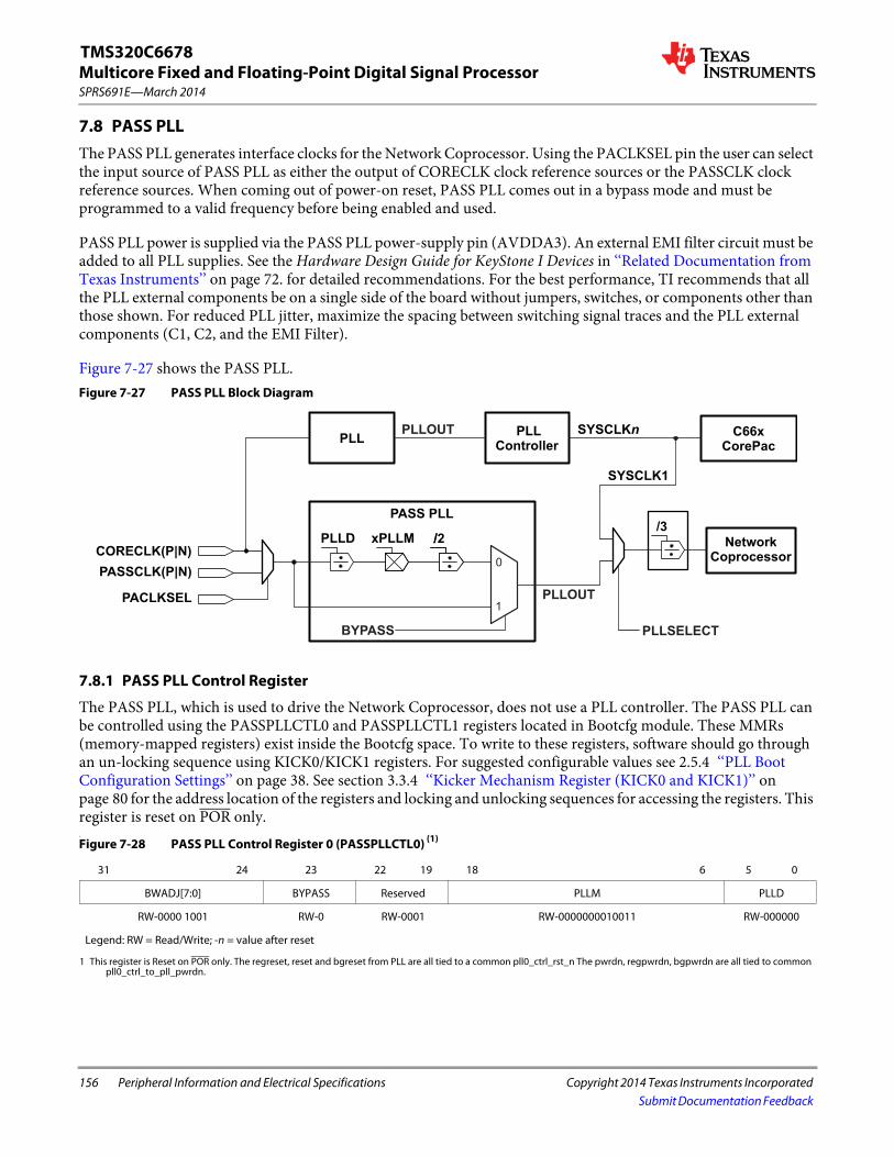
156 Peripheral Information and Electrical Specifications Copyright 2014 Texas Instruments Incorporated
SPRS691E—March 2014Multicore Fixed and Floating-Point Digital Signal ProcessorTMS320C6678
Submit Documentation Feedback
7.8 PASS PLLThe PASS PLL generates interface clocks for the Network Coprocessor. Using the PACLKSEL pin the user can select the input source of PASS PLL as either the output of CORECLK clock reference sources or the PASSCLK clock reference sources. When coming out of power-on reset, PASS PLL comes out in a bypass mode and must be programmed to a valid frequency before being enabled and used.
PASS PLL power is supplied via the PASS PLL power-supply pin (AVDDA3). An external EMI filter circuit must be added to all PLL supplies. See the Hardware Design Guide for KeyStone I Devices in ‘‘Related Documentation from Texas Instruments’’ on page 72. for detailed recommendations. For the best performance, TI recommends that all the PLL external components be on a single side of the board without jumpers, switches, or components other than those shown. For reduced PLL jitter, maximize the spacing between switching signal traces and the PLL external components (C1, C2, and the EMI Filter).
Figure 7-27 shows the PASS PLL.Figure 7-27 PASS PLL Block Diagram
7.8.1 PASS PLL Control Register
The PASS PLL, which is used to drive the Network Coprocessor, does not use a PLL controller. The PASS PLL can be controlled using the PASSPLLCTL0 and PASSPLLCTL1 registers located in Bootcfg module. These MMRs (memory-mapped registers) exist inside the Bootcfg space. To write to these registers, software should go through an un-locking sequence using KICK0/KICK1 registers. For suggested configurable values see 2.5.4 ‘‘PLL Boot Configuration Settings’’ on page 38. See section 3.3.4 ‘‘Kicker Mechanism Register (KICK0 and KICK1)’’ on page 80 for the address location of the registers and locking and unlocking sequences for accessing the registers. This register is reset on POR only..Figure 7-28 PASS PLL Control Register 0 (PASSPLLCTL0) (1)
1 This register is Reset on POR only. The regreset, reset and bgreset from PLL are all tied to a common pll0_ctrl_rst_n The pwrdn, regpwrdn, bgpwrdn are all tied to common pll0_ctrl_to_pll_pwrdn.
31 24 23 22 19 18 6 5 0
BWADJ[7:0] BYPASS Reserved PLLM PLLD
RW-0000 1001 RW-0 RW-0001 RW-0000000010011 RW-000000
Legend: RW = Read/Write; -n = value after reset
PASSCLK(P|N)
PACLKSEL
C66xCorePac
NetworkCoprocessor
SYSCLKn
/3
PLLOUT PLLController
PLL
1
0
/2xPLLMPLLD
PASS PLL
BYPASS
/
PLLOUT
SYSCLK1
PLLSELECT
CORECLK(P|N)

Multicore Fixed and Floating-Point Digital Signal Processor
Copyright 2014 Texas Instruments Incorporated Peripheral Information and Electrical Specifications 157
SPRS691E—March 2014
TMS320C6678
Submit Documentation Feedback
7.8.2 PASS PLL Device-Specific Information
As shown in Figure 7-27, the output of PASS PLL (PLLOUT) is divided by 2 and directly fed to the Network Coprocessor. The PASS PLL is affected by power-on reset. During power-on resets, the internal clocks of the PASS PLL are affected as described in Section 7.5 ‘‘Reset Controller’’ on page 133. The PASS PLL is unlocked only during the power-up sequence and is locked by the time the RESETSTAT pin goes high. It does not lose lock during any of the other resets.
7.8.3 PASS PLL Initialization Sequence
See the Phase Locked Loop (PLL) for KeyStone Devices User Guide in ‘‘Related Documentation from Texas Instruments’’ on page 72 for details on the initialization sequence for PASS PLL.
Table 7-30 PASS PLL Control Register 0 Field Descriptions
Bit Field Description
31-24 BWADJ[7:0] BWADJ[11:8] and BWADJ[7:0] are located in PASSPLLCTL0 and PASSPLLCTL1 registers. The combination (BWADJ[11:0]) should be programmed to a value related to PLLM[12:0] value based on the equation: BWADJ = ((PLLM+1)>>1) - 1
23 BYPASS Enable bypass mode0 = Bypass disabled1 = Bypass enabled
22-19 Reserved Reserved
18-6 PLLM A 13-bit bus that selects the values for the multiplication factor
5-0 PLLD A 6-bit bus that selects the values for the reference divider
End of Table 7-30
Figure 7-29 PASS PLL Control Register 1 (PASSPLLCTL1)
31 15 14 13 12 7 6 5 4 3 0
Reserved PLLRST PLLSELECT Reserved ENSAT Reserved BWADJ[11:8]
RW-00000000000000000 RW-0 RW-0 RW-000000 RW-0 R-0 RW-0000
Legend: RW = Read/Write; -n = value after reset
Table 7-31 PASS PLL Control Register 1 Field Descriptions
Bit Field Description
31-15 Reserved Reserved
14 PLLRST PLL reset bit.0 = PLL reset is released1 = PLL reset is asserted
13 PLLSELECT PASS PLL select bit. Note that this bit must be set before the Ethernet subsystem is configured and used.0 = Reserved1 = PASS PLL output clock is used as the input to PASS
12-7 Reserved Reserved
6 ENSAT Must be set to 1 for proper operation of the PLL
5-4 Reserved Reserved
3-0 BWADJ[11:8] BWADJ[11:8] and BWADJ[7:0] are located in PASSPLLCTL0 and PASSPLLCTL1 registers. The combination (BWADJ[11:0]) should be programmed to a value related to PLLM[12:0] value based on the equation: BWADJ = ((PLLM+1)>>1) - 1
End of Table 7-31

158 Peripheral Information and Electrical Specifications Copyright 2014 Texas Instruments Incorporated
SPRS691E—March 2014Multicore Fixed and Floating-Point Digital Signal ProcessorTMS320C6678
Submit Documentation Feedback
7.8.4 PASS PLL Input Clock Electrical Data/Timing
Figure 7-30 PASS PLL Timing
Table 7-32 PASS PLL Timing Requirements(See Figure 7-30 and Figure 7-22)
No. Min Max Unit
PASSCLK[P:N]
1 tc(PASSCLKN) Cycle Time _ PASSCLKN cycle time 3.2 25 ns
1 tc(PASSCLKP) Cycle Time _ PASSCLKP cycle time 3.2 25 ns
3 tw(PASSCLKN) Pulse Width _ PASSCLKN high 0.45*tc(PASSCLKN) 0.55*tc(PASSCLKN) ns
2 tw(PASSCLKN) Pulse Width _ PASSCLKN low 0.45*tc(PASSCLKN) 0.55*tc(PASSCLKN) ns
2 tw(PASSCLKP) Pulse Width _ PASSCLKP high 0.45*tc(PASSCLKP) 0.55*tc(PASSCLKP) ns
3 tw(PASSCLKP) Pulse Width _ PASSCLKP low 0.45*tc(PASSCLKP) 0.55*tc(PASSCLKP) ns
4 tr(PASSCLK_250mv) Transition time _ PASSCLK differential rise time (250 mV) 50 350 ps
4 tf(PASSCLK_250mv) Transition time _ PASSCLK differential fall time (250 mV) 50 350 ps
5 tj(PASSCLKN) Jitter, peak_to_peak _ periodic PASSCLKN 0.02*tc(PASSCLKN) ps, pk-pk
5 tj(PASSCLKP) Jitter, peak_to_peak _ periodic PASSCLKP 0.02*tc(PASSCLKP) ps, pk-pk
4
32
1
5
PASSCLKN
PASSCLKP
Multicore Fixed and Floating-Point Digital Signal Processor
Copyright 2014 Texas Instruments Incorporated Peripheral Information and Electrical Specifications 159
SPRS691E—March 2014
TMS320C6678
Submit Documentation Feedback
7.9 Enhanced Direct Memory Access (EDMA3) ControllerThe primary purpose of the EDMA3 is to service user-programmed data transfers between two memory-mapped slave endpoints on the device. The EDMA3 services software-driven paging transfers (e.g., data movement between external memory and internal memory), performs sorting or subframe extraction of various data structures, services event driven peripherals, and offloads data transfers from the device CPU.
There are 3 EDMA Channel Controllers on the C6678 DSP, EDMA3CC0, EDMA3CC1, and EDMA3CC2.• EDMA3CC0 has two transfer controllers: EDMA3TC1 and EDMA3TC2. • EDMA3CC1 has four transfer controllers: EDMA3TC0, EDMA3TC1, EDMA3TC2, and EDMA3TC3. • EDMA3CC2 has four transfer controllers: EDMA3TC0, EDMA3TC1, EDMA3TC2, and EDMA3TC3.
In the context of this document, EDMA3TCx associated with EDMA3CCy, and is referred to as EDMA3CCy TCx. Each of the transfer controllers has a direct connection to the switch fabric. Section 4.2 ‘‘Switch Fabric Connections’’ lists the peripherals that can be accessed by the transfer controllers.
EDMA3CC0 is optimized to be used for transfers to/from/within the MSMC and DDR-3 subsytems. The others are to be used for the remaining traffic.
Each EDMA3 Channel Controller includes the following features: • Fully orthogonal transfer description
– Three transfer dimensions: › Array (multiple bytes)› Frame (multiple arrays)› Block (multiple frames)
– Single event can trigger transfer of array, frame, or entire block – Independent indexes on source and destination
• Flexible transfer definition:– Increment or FIFO transfer addressing modes – Linking mechanism allows for ping-pong buffering, circular buffering, and repetitive/continuous
transfers, all with no CPU intervention – Chaining allows multiple transfers to execute with one event
• 128 PaRAM entries for EDMA3CC0, 512 each for EDMA3CC1 and EDMA3CC2– Used to define transfer context for channels – Each PaRAM entry can be used as a DMA entry, QDMA entry, or link entry
• 16 DMA channels for EDMA3CC0, 64 each for EDMA3CC1 and EDMA3CC2– Manually triggered (CPU writes to channel controller register), external event triggered, and chain
triggered (completion of one transfer triggers another)• 8 Quick DMA (QDMA) channels per EDMA 3 Channel Controller
– Used for software-driven transfers– Triggered upon writing to a single PaRAM set entry
• Two transfer controllers and two event queues with programmable system-level priority for EDMA3CC0, four transfer controllers and four event queues with programmable system-level priority per channel controller for EDMA3CC1 and EDMA3CC2
• Interrupt generation for transfer completion and error conditions
160 Peripheral Information and Electrical Specifications Copyright 2014 Texas Instruments Incorporated
SPRS691E—March 2014Multicore Fixed and Floating-Point Digital Signal ProcessorTMS320C6678
Submit Documentation Feedback
• Debug visibility– Queue watermarking/threshold allows detection of maximum usage of event queues– Error and status recording to facilitate debug
7.9.1 EDMA3 Device-Specific Information
The EDMA supports two addressing modes: constant addressing and increment addressing mode. Constant addressing mode is applicable to a very limited set of use cases. For most applications, increment mode must be used. For more information on these two addressing modes, see the Enhanced Direct Memory Access 3 (EDMA3) Controller for KeyStone Devices User Guide in ‘‘Related Documentation from Texas Instruments’’ on page 72.
For the range of memory addresses that include EDMA3 channel controller (EDMA3CC) control registers and EDMA3 transfer controller (EDMA3TC) control register see Section Table 2-2‘‘Memory Map Summary’’ on page 17. For memory offsets and other details on EDMA3CC and EDMA3TC control registers entries, see the Enhanced Direct Memory Access 3 (EDMA3) Controller for KeyStone Devices User Guide in ‘‘Related Documentation from Texas Instruments’’ on page 72.
7.9.2 EDMA3 Channel Controller Configuration
Table 7-33 shows the configuration for each of the EDMA3 channel controllers present on the device.
7.9.3 EDMA3 Transfer Controller Configuration
Each transfer controller on a device is designed differently based on considerations like performance requirements, system topology (like main TeraNet bus width, external memory bus width), etc. The parameters that determine the transfer controller configurations are:
• FIFOSIZE: Determines the size in bytes for the data FIFO that is the temporary buffer for the in-flight data. The data FIFO is where the read return data read by the TC read controller from the source endpoint is stored and subsequently written out to the destination endpoint by the TC write controller.
• BUSWIDTH: The width of the read and write data buses in bytes, for the TC read and write controller, respectively. This is typically equal to the bus width of the main TeraNet interface.
• Default Burst Size (DBS): The DBS is the maximum number of bytes per read/write command issued by a transfer controller.
• DSTREGDEPTH: This determines the number of destination FIFO register set. The number of destination FIFO register set for a transfer controller determines the maximum number of outstanding transfer requests.
All four parameters listed above are fixed by the design of the device.
Table 7-34 shows the configuration for each of the EDMA3 transfer controllers present on the device.
Table 7-33 EDMA3 Channel Controller Configuration
Description EDMA3 CC0 EDMA3 CC1 EDMA3 CC2
Number of DMA channels in Channel Controller 16 64 64
Number of QDMA channels 8 8 8
Number of interrupt channels 16 64 64
Number of PaRAM set entries 128 512 512
Number of event queues 2 4 4
Number of Transfer Controllers 2 4 4
Memory Protection Existence Yes Yes Yes
Number of Memory Protection and Shadow Regions 8 8 8
End of Table 7-33

Multicore Fixed and Floating-Point Digital Signal Processor
Copyright 2014 Texas Instruments Incorporated Peripheral Information and Electrical Specifications 161
SPRS691E—March 2014
TMS320C6678
Submit Documentation Feedback
7.9.4 EDMA3 Channel Synchronization Events
The EDMA3 supports up to 16 DMA channels for EDMA3CC0, 64 each for EDMA3CC1 and EDMA3CC2 that can be used to service system peripherals and to move data between system memories. DMA channels can be triggered by synchronization events generated by system peripherals. The following tables lists the source of the synchronization event associated with each of the EDMA EDMA3CC DMA channels. On the C6678, the association of each synchronization event and DMA channel is fixed and cannot be reprogrammed.
For more detailed information on the EDMA3 module and how EDMA3 events are enabled, captured, processed, prioritized, linked, chained, and cleared, etc., see the Enhanced Direct Memory Access 3 (EDMA3) Controller for KeyStone Devices User Guide in ‘‘Related Documentation from Texas Instruments’’ on page 72.
Table 7-34 EDMA3 Transfer Controller Configuration
Parameter
EDMA3 CC0 EDMA3 CC1 EDMA3 CC2
TC0 TC1 TC0 TC1 TC2 TC3 TC0 TC1 TC2 TC3
FIFOSIZE 1024 bytes 1024 bytes 1024 bytes 512 bytes 1024 bytes 512 bytes 1024 bytes 512 bytes 512 bytes 1024 bytes
BUSWIDTH 32 bytes 32 bytes 16 bytes 16 bytes 16 bytes 16 bytes 16 bytes 16 bytes 16 bytes 16 bytes
DSTREGDEPTH 4 entries 4 entries 4 entries 4 entries 4 entries 4 entries 4 entries 4 entries 4 entries 4 entries
DBS 128 bytes 128 bytes 128 bytes 64 bytes 128 bytes 64 bytes 128 bytes 64 bytes 64 bytes 128 bytes
End of Table 7-34
Table 7-35 EDMA3CC0 Events for C6678
Event Number Event Event Description
0 TINT8L Timer interrupt low
1 TINT8H Timer interrupt high
2 TINT9L Timer interrupt low
3 TINT9H Timer interrupt high
4 TINT10L Timer interrupt low
5 TINT10H Timer interrupt high
6 TINT11L Timer interrupt low
7 TINT11H Timer interrupt high
8 CIC3_OUT0 Interrupt Controller output
9 CIC3_OUT1 Interrupt Controller output
10 CIC3_OUT2 Interrupt Controller output
11 CIC3_OUT3 Interrupt Controller output
12 CIC3_OUT4 Interrupt Controller output
13 CIC3_OUT5 Interrupt Controller output
14 CIC3_OUT6 Interrupt Controller output
15 CIC3_OUT7 Interrupt Controller output
End of Table 7-35
Table 7-36 EDMA3CC1 Events for C6678 (Sheet 1 of 3)
Event Number Event Event Description
0 SPIINT0 SPI interrupt
1 SPIINT1 SPI interrupt
2 SPIXEVT Transmit event
3 SPIREVT Receive event
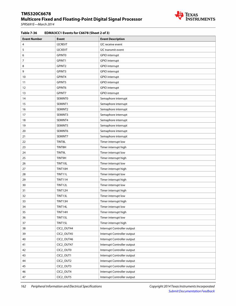
162 Peripheral Information and Electrical Specifications Copyright 2014 Texas Instruments Incorporated
SPRS691E—March 2014Multicore Fixed and Floating-Point Digital Signal ProcessorTMS320C6678
Submit Documentation Feedback
4 I2CREVT I2C receive event
5 I2CXEVT I2C transmit event
6 GPINT0 GPIO interrupt
7 GPINT1 GPIO interrupt
8 GPINT2 GPIO interrupt
9 GPINT3 GPIO interrupt
10 GPINT4 GPIO interrupt
11 GPINT5 GPIO interrupt
12 GPINT6 GPIO interrupt
13 GPINT7 GPIO interrupt
14 SEMINT0 Semaphore interrupt
15 SEMINT1 Semaphore interrupt
16 SEMINT2 Semaphore interrupt
17 SEMINT3 Semaphore interrupt
18 SEMINT4 Semaphore interrupt
19 SEMINT5 Semaphore interrupt
20 SEMINT6 Semaphore interrupt
21 SEMINT7 Semaphore interrupt
22 TINT8L Timer interrupt low
23 TINT8H Timer interrupt high
24 TINT9L Timer interrupt low
25 TINT9H Timer interrupt high
26 TINT10L Timer interrupt low
27 TINT10H Timer interrupt high
28 TINT11L Timer interrupt low
29 TINT11H Timer interrupt high
30 TINT12L Timer interrupt low
31 TINT12H Timer interrupt high
32 TINT13L Timer interrupt low
33 TINT13H Timer interrupt high
34 TINT14L Timer interrupt low
35 TINT14H Timer interrupt high
36 TINT15L Timer interrupt low
37 TINT15L Timer interrupt high
38 CIC2_OUT44 Interrupt Controller output
39 CIC2_OUT45 Interrupt Controller output
40 CIC2_OUT46 Interrupt Controller output
41 CIC2_OUT47 Interrupt Controller output
42 CIC2_OUT0 Interrupt Controller output
43 CIC2_OUT1 Interrupt Controller output
44 CIC2_OUT2 Interrupt Controller output
45 CIC2_OUT3 Interrupt Controller output
46 CIC2_OUT4 Interrupt Controller output
47 CIC2_OUT5 Interrupt Controller output
Table 7-36 EDMA3CC1 Events for C6678 (Sheet 2 of 3)
Event Number Event Event Description
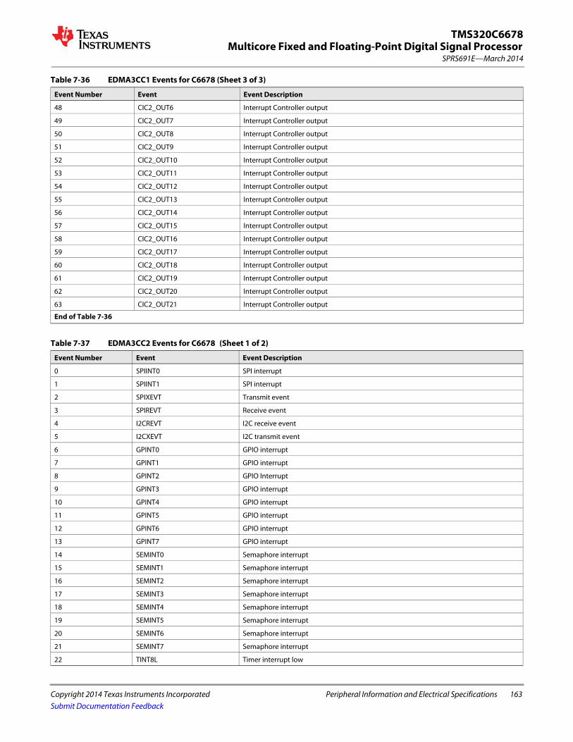
Multicore Fixed and Floating-Point Digital Signal Processor
Copyright 2014 Texas Instruments Incorporated Peripheral Information and Electrical Specifications 163
SPRS691E—March 2014
TMS320C6678
Submit Documentation Feedback
48 CIC2_OUT6 Interrupt Controller output
49 CIC2_OUT7 Interrupt Controller output
50 CIC2_OUT8 Interrupt Controller output
51 CIC2_OUT9 Interrupt Controller output
52 CIC2_OUT10 Interrupt Controller output
53 CIC2_OUT11 Interrupt Controller output
54 CIC2_OUT12 Interrupt Controller output
55 CIC2_OUT13 Interrupt Controller output
56 CIC2_OUT14 Interrupt Controller output
57 CIC2_OUT15 Interrupt Controller output
58 CIC2_OUT16 Interrupt Controller output
59 CIC2_OUT17 Interrupt Controller output
60 CIC2_OUT18 Interrupt Controller output
61 CIC2_OUT19 Interrupt Controller output
62 CIC2_OUT20 Interrupt Controller output
63 CIC2_OUT21 Interrupt Controller output
End of Table 7-36
Table 7-37 EDMA3CC2 Events for C6678 (Sheet 1 of 2)
Event Number Event Event Description
0 SPIINT0 SPI interrupt
1 SPIINT1 SPI interrupt
2 SPIXEVT Transmit event
3 SPIREVT Receive event
4 I2CREVT I2C receive event
5 I2CXEVT I2C transmit event
6 GPINT0 GPIO interrupt
7 GPINT1 GPIO interrupt
8 GPINT2 GPIO Interrupt
9 GPINT3 GPIO interrupt
10 GPINT4 GPIO interrupt
11 GPINT5 GPIO interrupt
12 GPINT6 GPIO interrupt
13 GPINT7 GPIO interrupt
14 SEMINT0 Semaphore interrupt
15 SEMINT1 Semaphore interrupt
16 SEMINT2 Semaphore interrupt
17 SEMINT3 Semaphore interrupt
18 SEMINT4 Semaphore interrupt
19 SEMINT5 Semaphore interrupt
20 SEMINT6 Semaphore interrupt
21 SEMINT7 Semaphore interrupt
22 TINT8L Timer interrupt low
Table 7-36 EDMA3CC1 Events for C6678 (Sheet 3 of 3)
Event Number Event Event Description

164 Peripheral Information and Electrical Specifications Copyright 2014 Texas Instruments Incorporated
SPRS691E—March 2014Multicore Fixed and Floating-Point Digital Signal ProcessorTMS320C6678
Submit Documentation Feedback
23 TINT8H Timer interrupt high
24 TINT9L Timer interrupt low
25 TINT9H Timer interrupt high
26 TINT10L Timer interrupt low
27 TINT10H Timer interrupt high
28 TINT11L Timer interrupt low
29 TINT11H Timer interrupt high
30 TINT12L Timer interrupt low
31 TINT12H Timer interrupt high
32 TINT13L Timer interrupt low
33 TINT13H Timer interrupt high
34 TINT14L Timer interrupt low
35 TINT14H Timer interrupt high
36 TINT15L Timer interrupt low
37 TINT15H Timer interrupt high
38 CIC2_OUT48 Interrupt Controller output
39 CIC2_OUT49 Interrupt Controller output
40 URXEVT UART receive event
41 UTXEVT UART transmit event
42 CIC2_OUT22 Interrupt Controller output
43 CIC2_OUT23 Interrupt Controller output
44 CIC2_OUT24 Interrupt Controller output
45 CIC2_OUT25 Interrupt Controller output
46 CIC2_OUT26 Interrupt Controller output
47 CIC2_OUT27 Interrupt Controller output
48 CIC2_OUT28 Interrupt Controller output
49 CIC2_OUT29 Interrupt Controller output
50 CIC2_OUT30 Interrupt Controller output
51 CIC2_OUT31 Interrupt Controller output
52 CIC2_OUT32 Interrupt Controller output
53 CIC2_OUT33 Interrupt Controller output
54 CIC2_OUT34 Interrupt Controller output
55 CIC2_OUT35 Interrupt Controller output
56 CIC2_OUT36 Interrupt Controller output
57 CIC2_OUT37 Interrupt Controller output
58 CIC2_OUT38 Interrupt Controller output
59 CIC2_OUT39 Interrupt Controller output
60 CIC2_OUT40 Interrupt Controller output
61 CIC2_OUT41 Interrupt Controller output
62 CIC2_OUT42 Interrupt Controller output
63 CIC2_OUT43 Interrupt Controller output
End of Table 7-37
Table 7-37 EDMA3CC2 Events for C6678 (Sheet 2 of 2)
Event Number Event Event Description

Multicore Fixed and Floating-Point Digital Signal Processor
Copyright 2014 Texas Instruments Incorporated Peripheral Information and Electrical Specifications 165
SPRS691E—March 2014
TMS320C6678
Submit Documentation Feedback
7.10 Interrupts7.10.1 Interrupt Sources and Interrupt Controller
The CPU interrupts on the C6678 device are configured through the C66x CorePac Interrupt Controller. The interrupt controller allows for up to 128 system events to be programmed to any of the twelve CPU interrupt inputs (CPUINT4 - CPUINT15), the CPU exception input (EXCEP), or the advanced emulation logic. The 128 system events consist of both internally-generated events (within the CorePac) and chip-level events.
Additional system events are routed to each of the C66x CorePacs to provide chip-level events that are not required as CPU interrupts/exceptions to be routed to the interrupt controller as emulation events. Additionally, error-class events or infrequently used events are also routed through the system event router to offload the C66x CorePac interrupt selector. This is accomplished through chip interrupt controller (CIC) blocks. This is clocked using CPU/6.
The event controllers consist of simple combination logic to provide additional events to each C66x CorePac, plus the EDMA3CC, CIC0, and CIC1 provide 17 additional events as well as 8 broadcast events to each of the C66x CorePacs, CIC2 provides 26 and 24 additional events to EDMA3CC1 and EDMA3CC2 respectively, and CIC3 provides 8 and 32 additional events to EDMA3CC0 and HyperLink respectively.
There are a large number of events at the chip level. The chip level CIC provides a flexible way to combine and remap those events. Multiple events can be combined to a single event through chip level CIC. However, an event can be mapped only to a single event output from the chip level CIC. The chip level CIC also allows the software to trigger system event through memory writes. The broadcast events to C66x CorePacs can be used for synchronization among multiple cores or inter-processor communication purpose and etc. For more details on the CIC features, see the Chip Interrupt Controller (CIC) for KeyStone Devices User Guide in ‘‘Related Documentation from Texas Instruments’’ on page 72.
Note—Modules such as MPU, Tracer, and BOOT_CFG have level interrupts and EOI handshaking interface. The EOI value is 0 for MPU, Tracer, and BOOT_CFG.

166 Peripheral Information and Electrical Specifications Copyright 2014 Texas Instruments Incorporated
SPRS691E—March 2014Multicore Fixed and Floating-Point Digital Signal ProcessorTMS320C6678
Submit Documentation Feedback
Figure 7-31 shows the C6678 interrupt topology.Figure 7-31 TMS320C6678 Interrupt Topology
CIC2
63 Common Events
HyperLink
26 Secondary Events
32 Secondary Events
8 Secondary Events
88 EDMA3CC-onlySecondary Events
38 Primary Events
40 Primary Events
24 Secondary Events
CIC3
8 Primary Events63 Events
9 Reserved Secondary Events
17 Reserved Secondary Events
EDMA3CC0
EDMA3CC2
EDMA3CC1
CIC1
8 Broadcast Events from CIC1
Core5
Core6
Core7
Core4
98 Primary Events
17 Secondary Events
17 Secondary Events
17 Secondary Events
17 Secondary Events
98 Primary Events
98 Primary Events
98 Primary Events
5 Reserved Primary Events
5 Reserved Primary Events
5 Reserved Primary Events
5 Reserved Primary Events
89 Core-only Secondary Events
63 Common Events
8 Reserved Secondary Events
32 Primary Events
CIC0
8 Broadcast Events from CIC0
Core1
Core2
Core3
Core0
98 Primary Events
17 Secondary Events
17 Secondary Events
17 Secondary Events
17 Secondary Events
98 Primary Events
98 Primary Events
98 Primary Events
5 Reserved Primary Events
5 Reserved Primary Events
5 Reserved Primary Events
5 Reserved Primary Events
89 Core-only Secondary Events
63 Common Events
8 Reserved Secondary Events
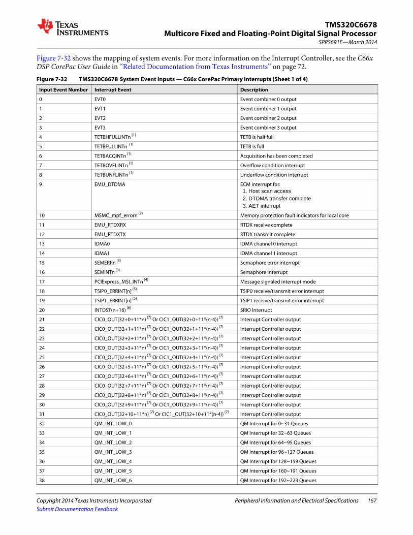
Multicore Fixed and Floating-Point Digital Signal Processor
Copyright 2014 Texas Instruments Incorporated Peripheral Information and Electrical Specifications 167
SPRS691E—March 2014
TMS320C6678
Submit Documentation Feedback
Figure 7-32 shows the mapping of system events. For more information on the Interrupt Controller, see the C66x DSP CorePac User Guide in ‘‘Related Documentation from Texas Instruments’’ on page 72.Figure 7-32 TMS320C6678 System Event Inputs — C66x CorePac Primary Interrupts (Sheet 1 of 4)
Input Event Number Interrupt Event Description
0 EVT0 Event combiner 0 output
1 EVT1 Event combiner 1 output
2 EVT2 Event combiner 2 output
3 EVT3 Event combiner 3 output
4 TETBHFULLINTn (1) TETB is half full
5 TETBFULLINTn (1) TETB is full
6 TETBACQINTn (1) Acquisition has been completed
7 TETBOVFLINTn (1) Overflow condition interrupt
8 TETBUNFLINTn (1) Underflow condition interrupt
9 EMU_DTDMA ECM interrupt for:1. Host scan access2. DTDMA transfer complete3. AET interrupt
10 MSMC_mpf_errorn (2) Memory protection fault indicators for local core
11 EMU_RTDXRX RTDX receive complete
12 EMU_RTDXTX RTDX transmit complete
13 IDMA0 IDMA channel 0 interrupt
14 IDMA1 IDMA channel 1 interrupt
15 SEMERRn (3) Semaphore error interrupt
16 SEMINTn (3) Semaphore interrupt
17 PCIExpress_MSI_INTn (4) Message signaled interrupt mode
18 TSIP0_ERRINT[n] (5) TSIP0 receive/transmit error interrupt
19 TSIP1_ERRINT[n] (5) TSIP1 receive/transmit error interrupt
20 INTDST(n+16) (6) SRIO Interrupt
21 CIC0_OUT(32+0+11*n) (7) Or CIC1_OUT(32+0+11*(n-4)) (7) Interrupt Controller output
22 CIC0_OUT(32+1+11*n) (7) Or CIC1_OUT(32+1+11*(n-4)) (7) Interrupt Controller output
23 CIC0_OUT(32+2+11*n) (7) Or CIC1_OUT(32+2+11*(n-4)) (7) Interrupt Controller output
24 CIC0_OUT(32+3+11*n) (7) Or CIC1_OUT(32+3+11*(n-4)) (7) Interrupt Controller output
25 CIC0_OUT(32+4+11*n) (7) Or CIC1_OUT(32+4+11*(n-4)) (7) Interrupt Controller output
26 CIC0_OUT(32+5+11*n) (7) Or CIC1_OUT(32+5+11*(n-4)) (7) Interrupt Controller output
27 CIC0_OUT(32+6+11*n) (7) Or CIC1_OUT(32+6+11*(n-4)) (7) Interrupt Controller output
28 CIC0_OUT(32+7+11*n) (7) Or CIC1_OUT(32+7+11*(n-4)) (7) Interrupt Controller output
29 CIC0_OUT(32+8+11*n) (7) Or CIC1_OUT(32+8+11*(n-4)) (7) Interrupt Controller output
30 CIC0_OUT(32+9+11*n) (7) Or CIC1_OUT(32+9+11*(n-4)) (7) Interrupt Controller output
31 CIC0_OUT(32+10+11*n) (7) Or CIC1_OUT(32+10+11*(n-4)) (7) Interrupt Controller output
32 QM_INT_LOW_0 QM Interrupt for 0~31 Queues
33 QM_INT_LOW_1 QM Interrupt for 32~63 Queues
34 QM_INT_LOW_2 QM Interrupt for 64~95 Queues
35 QM_INT_LOW_3 QM Interrupt for 96~127 Queues
36 QM_INT_LOW_4 QM Interrupt for 128~159 Queues
37 QM_INT_LOW_5 QM Interrupt for 160~191 Queues
38 QM_INT_LOW_6 QM Interrupt for 192~223 Queues
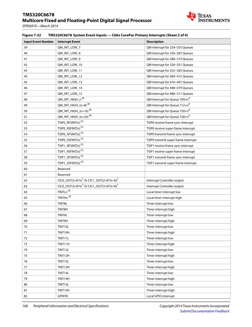
168 Peripheral Information and Electrical Specifications Copyright 2014 Texas Instruments Incorporated
SPRS691E—March 2014Multicore Fixed and Floating-Point Digital Signal ProcessorTMS320C6678
Submit Documentation Feedback
39 QM_INT_LOW_7 QM Interrupt for 224~255 Queues
40 QM_INT_LOW_8 QM Interrupt for 256~287 Queues
41 QM_INT_LOW_9 QM Interrupt for 288~319 Queues
42 QM_INT_LOW_10 QM Interrupt for 320~351 Queues
43 QM_INT_LOW_11 QM Interrupt for 352~383 Queues
44 QM_INT_LOW_12 QM Interrupt for 384~415 Queues
45 QM_INT_LOW_13 QM Interrupt for 416~447 Queues
46 QM_INT_LOW_14 QM Interrupt for 448~479 Queues
47 QM_INT_LOW_15 QM Interrupt for 480~511 Queues
48 QM_INT_HIGH_n (8) QM Interrupt for Queue 704+n8
49 QM_INT_HIGH_(n+8) (8) QM Interrupt for Queue 712+n8
50 QM_INT_HIGH_(n+16) (8) QM Interrupt for Queue 720+n8
51 QM_INT_HIGH_(n+24) (8) QM Interrupt for Queue 728+n8
52 TSIP0_RFSINT[n] (5) TSIP0 receive frame sync interrupt
53 TSIP0_RSFINT[n] (5) TSIP0 receive super frame interrupt
54 TSIP0_XFSINT[n] (5) TSIP0 transmit frame sync interrupt
55 TSIP0_XSFINT[n] (5) TSIP0 transmit super frame interrupt
56 TSIP1_RFSINT[n] (5) TSIP1 receive frame sync interrupt
57 TSIP1_RSFINT[n] (5) TSIP1 receive super frame interrupt
58 TSIP1_XFSINT[n] (5) TSIP1 transmit frame sync interrupt
59 TSIP1_XSFINT[n] (5) TSIP1 transmit super frame interrupt
60 Reserved
61 Reserved
62 CIC0_OUT(2+8*n)7 Or CIC1_OUT(2+8*(n-4))7 Interrupt Controller output
63 CIC0_OUT(3+8*n)7 Or CIC1_OUT(3+8*(n-4))7 Interrupt Controller output
64 TINTLn (9) Local timer interrupt low
65 TINTHn (9) Local timer interrupt high
66 TINT8L Timer interrupt low
67 TINT8H Timer interrupt high
68 TINT9L Timer interrupt low
69 TINT9H Timer interrupt high
70 TINT10L Timer interrupt low
71 TINT10H Timer interrupt high
72 TINT11L Timer interrupt low
73 TINT11H Timer interrupt high
74 TINT12L Timer interrupt low
75 TINT12H Timer interrupt high
76 TINT13L Timer interrupt low
77 TINT13H Timer interrupt high
78 TINT14L Timer interrupt low
79 TINT14H Timer interrupt high
80 TINT15L Timer interrupt low
81 TINT15H Timer interrupt high
82 GPINT8 Local GPIO interrupt
Figure 7-32 TMS320C6678 System Event Inputs — C66x CorePac Primary Interrupts (Sheet 2 of 4)
Input Event Number Interrupt Event Description

Multicore Fixed and Floating-Point Digital Signal Processor
Copyright 2014 Texas Instruments Incorporated Peripheral Information and Electrical Specifications 169
SPRS691E—March 2014
TMS320C6678
Submit Documentation Feedback
83 GPINT9 Local GPIO interrupt
84 GPINT10 Local GPIO interrupt
85 GPINT11 Local GPIO interrupt
86 GPINT12 Local GPIO interrupt
87 GPINT13 Local GPIO interrupt
88 GPINT14 Local GPIO interrupt
89 GPINT15 Local GPIO interrupt
90 GPINTn (10) Local GPIO interrupt
91 IPC_LOCAL Inter DSP interrupt from IPCGRn
92 CIC0_OUT(4+8*n) (7) Or CIC1_OUT(4+8*(n-4)) (7) Interrupt Controller output
93 CIC0_OUT(5+8*n) (7) Or CIC1_OUT(5+8*(n-4)) (7) Interrupt Controller output
94 CIC0_OUT(6+8*n) (7) Or CIC1_OUT(6+8*(n-4)) (7) Interrupt Controller output
95 CIC0_OUT(7+8*n) (7) Or CIC1_OUT(7+8*(n-4)) (7) Interrupt Controller output
96 INTERR Dropped CPU interrupt event
97 EMC_IDMAERR Invalid IDMA parameters
98 Reserved
99 Reserved
100 EFIINTA EFI Interrupt from side A
101 EFIINTB EFI Interrupt from side B
102 CIC0_OUT0 or CIC1_OUT0 Interrupt Controller output
103 CIC0_OUT1 or CIC1_OUT1 Interrupt Controller output
104 CIC0_OUT8 or CIC1_OUT8 Interrupt Controller output
105 CIC0_OUT9 or CIC1_OUT9 Interrupt Controller output
106 CIC0_OUT16 or CIC1_OUT16 Interrupt Controller output
107 CIC0_OUT17 or CIC1_OUT17 Interrupt Controller output
108 CIC0_OUT24 or CIC1_OUT24 Interrupt Controller output
109 CIC0_OUT25 or CIC1_OUT25 Interrupt Controller output
110 MDMAERREVT VbusM error event
111 Reserved
112 EDMA3CC0_EDMACC_AETEVT EDMA3CC0 AET event
113 PMC_ED Single bit error detected during DMA read
114 EDMA3CC1_EDMACC_AETEVT EDMA3CC1 AET Event
115 EDMA3CC2_EDMACC_AETEVT EDMA3CC2 AET Event
116 UMC_ED1 Corrected bit error detected
117 UMC_ED2 Uncorrected bit error detected
118 PDC_INT Power down sleep interrupt
119 SYS_CMPA SYS CPU memory protection fault event
120 PMC_CMPA PMC CPU memory protection fault event
121 PMC_DMPA PMC DMA memory protection fault event
122 DMC_CMPA DMC CPU memory protection fault event
123 DMC_DMPA DMC DMA memory protection fault event
124 UMC_CMPA UMC CPU memory protection fault event
125 UMC_DMPA UMC DMA memory protection fault event
Figure 7-32 TMS320C6678 System Event Inputs — C66x CorePac Primary Interrupts (Sheet 3 of 4)
Input Event Number Interrupt Event Description

170 Peripheral Information and Electrical Specifications Copyright 2014 Texas Instruments Incorporated
SPRS691E—March 2014Multicore Fixed and Floating-Point Digital Signal ProcessorTMS320C6678
Submit Documentation Feedback
126 EMC_CMPA EMC CPU memory protection fault event
127 EMC_BUSERR EMC bus error interrupt
End of Table 7-37
1 CorePac[n] will receive TETBHFULLINTn, TETBFULLINTn, TETBACQINTn, TETBOVFLINTn, and TETBUNFLINTn.2 CorePac[n] will receive MSMC_mpf_errorn.CIC.3 CorePac[n] will receive SEMINTn and SEMERRn.4 CorePac[n] will receive PCIEXpress_MSI_INTn.5 CorePac[n] will receive TSIPx_xxx[n].6 CorePac[n] will receive INTDST(n+16).7 n is core number.8 n is core number.9 CorePac[n] will receive TINTLn and TINTHn.10 CorePac[n] will receive GPINTn.
Table 7-38 CIC0 Event Inputs (Secondary Interrupts for C66x CorePacs) (Sheet 1 of 5)
Input Event# on CIC System Interrupt Description
0 EDMA3CC1 CC_ERRINT EDMA3CC1 error interrupt
1 EDMA3CC1 CC_MPINT EDMA3CC1 memory protection interrupt
2 EDMA3CC1 TC_ERRINT0 EDMA3CC1 TC0 error interrupt
3 EDMA3CC1 TC_ERRINT1 EDMA3CC1 TC1 error interrupt
4 EDMA3CC1 TC_ERRINT2 EDMA3CC1 TC2 error interrupt
5 EDMA3CC1 TC_ERRINT3 EDMA3CC1 TC3 error interrupt
6 EDMA3CC1 CC_GINT EDMA3CC1 GINT
7 Reserved
8 EDMA3CC1 CCINT0 EDMA3CC1 individual completion interrupt
9 EDMA3CC1 CCINT1 EDMA3CC1 individual completion interrupt
10 EDMA3CC1 CCINT2 EDMA3CC1 individual completion interrupt
11 EDMA3CC1 CCINT3 EDMA3CC1 individual completion interrupt
12 EDMA3CC1 CCINT4 EDMA3CC1 individual completion interrupt
13 EDMA3CC1 CCINT5 EDMA3CC1 individual completion interrupt
14 EDMA3CC1 CCINT6 EDMA3CC1 individual completion interrupt
15 EDMA3CC1 CCINT7 EDMA3CC1 individual completion interrupt
16 EDMA3CC2 CC_ERRINT EDMA3CC2 error interrupt
17 EDMA3CC2 CC_MPINT EDMA3CC2 memory protection interrupt
18 EDMA3CC2 TC_ERRINT0 EDMA3CC2 TC0 error interrupt
19 EDMA3CC2 TC_ERRINT1 EDMA3CC2 TC1 error interrupt
20 EDMA3CC2 TC_ERRINT2 EDMA3CC2 TC2 error interrupt
21 EDMA3CC2 TC_ERRINT3 EDMA3CC2 TC3 error interrupt
22 EDMA3CC2 CC_GINT EDMA3CC2 GINT
23 Reserved
24 EDMA3CC2 CCINT0 EDMA3CC2 individual completion interrupt
25 EDMA3CC2 CCINT1 EDMA3CC2 individual completion interrupt
26 EDMA3CC2 CCINT2 EDMA3CC2 individual completion interrupt
27 EDMA3CC2 CCINT3 EDMA3CC2 individual completion interrupt
28 EDMA3CC2 CCINT4 EDMA3CC2 individual completion interrupt
29 EDMA3CC2 CCINT5 EDMA3CC2 individual completion interrupt
Figure 7-32 TMS320C6678 System Event Inputs — C66x CorePac Primary Interrupts (Sheet 4 of 4)
Input Event Number Interrupt Event Description

Multicore Fixed and Floating-Point Digital Signal Processor
Copyright 2014 Texas Instruments Incorporated Peripheral Information and Electrical Specifications 171
SPRS691E—March 2014
TMS320C6678
Submit Documentation Feedback
30 EDMA3CC2 CCINT6 EDMA3CC2 individual completion interrupt
31 EDMA3CC2 CCINT7 EDMA3CC2 individual completion interrupt
32 EDMA3CC0 CC_ERRINT EDMA3CC0 error interrupt
33 EDMA3CC0 CC_MPINT EDMA3CC0 memory protection interrupt
34 EDMA3CC0 TC_ERRINT0 EDMA3CC0 TC0 error interrupt
35 EDMA3CC0 TC_ERRINT1 EDMA3CC0 TC1 error interrupt
36 EDMA3CC0 CC_GINT EDMA3CC0 GINT
37 Reserved
38 EDMA3CC0 CCINT0 EDMA3CC0 individual completion interrupt
39 EDMA3CC0 CCINT1 EDMA3CC0 individual completion interrupt
40 EDMA3CC0 CCINT2 EDMA3CC0 individual completion interrupt
41 EDMA3CC0 CCINT3 EDMA3CC0 individual completion interrupt
42 EDMA3CC0 CCINT4 EDMA3CC0 individual completion interrupt
43 EDMA3CC0 CCINT5 EDMA3CC0 individual completion interrupt
44 EDMA3CC0 CCINT6 EDMA3CC0 individual completion interrupt
45 EDMA3CC0 CCINT7 EDMA3CC0 individual completion interrupt
46 Reserved
47 QM_INT_PASS_TXQ_PEND_12 Queue manager pend event
48 PCIEXpress_ERR_INT Protocol error interrupt
49 PCIEXpress_PM_INT Power management interrupt
50 PCIEXpress_Legacy_INTA Legacy interrupt mode
51 PCIEXpress_Legacy_INTB Legacy interrupt mode
52 PCIEXpress_Legacy_INTC Legacy interrupt mode
53 PCIEXpress_Legacy_INTD Legacy interrupt mode
54 SPIINT0 SPI interrupt0
55 SPIINT1 SPI interrupt1
56 SPIXEVT Transmit event
57 SPIREVT Receive event
58 I2CINT I2C interrupt
59 I2CREVT I2C receive event
60 I2CXEVT I2C transmit event
61 Reserved
62 Reserved
63 TETBHFULLINT TETB is half full
64 TETBFULLINT TETB is full
65 TETBACQINT Acquisition has been completed
66 TETBOVFLINT Overflow condition occur
67 TETBUNFLINT Underflow condition occur
68 MDIO_LINK_INTR0 Network coprocessor MDIO interrupt
69 MDIO_LINK_INTR1 Network coprocessor MDIO interrupt
70 MDIO_USER_INTR0 Network coprocessor MDIO interrupt
71 MDIO_USER_INTR1 Network coprocessor MDIO interrupt
72 MISC_INTR Network coprocessor MISC interrupt
Table 7-38 CIC0 Event Inputs (Secondary Interrupts for C66x CorePacs) (Sheet 2 of 5)
Input Event# on CIC System Interrupt Description

172 Peripheral Information and Electrical Specifications Copyright 2014 Texas Instruments Incorporated
SPRS691E—March 2014Multicore Fixed and Floating-Point Digital Signal ProcessorTMS320C6678
Submit Documentation Feedback
73 TRACER_CORE_0_INTD Tracer sliding time window interrupt for individual core
74 TRACER_CORE_1_INTD Tracer sliding time window interrupt for individual core
75 TRACER_CORE_2_INTD Tracer sliding time window interrupt for individual core
76 TRACER_CORE_3_INTD Tracer sliding time window interrupt for individual core
77 TRACER_DDR_INTD Tracer sliding time window interrupt for DDR3 EMIF1
78 TRACER_MSMC_0_INTD Tracer sliding time window interrupt for MSMC SRAM bank0
79 TRACER_MSMC_1_INTD Tracer sliding time window interrupt for MSMC SRAM bank1
80 TRACER_MSMC_2_INTD Tracer sliding time window interrupt for MSMC SRAM bank2
81 TRACER_MSMC_3_INTD Tracer sliding time window interrupt for MSMC SRAM bank3
81 TRACER_CFG_INTD Tracer sliding time window interrupt for CFG0 TeraNet
82 TRACER_QM_CFG_INTD Tracer sliding time window interrupt for QM_SS CFG
84 TRACER_QM_DMA_INTD Tracer sliding time window interrupt for QM_SS slave
85 TRACER_SM_INTD Tracer sliding time window interrupt for semaphore
86 PSC_ALLINT Power/sleep controller interrupt
87 MSMC_SCRUB_CERROR Correctable (1-bit) soft error detected during scrub cycle
88 BOOTCFG_INTD Chip-level MMR error register
89 Reserved
90 MPU0_INTD (MPU0_ADDR_ERR_INT and MPU0_PROT_ERR_INT combined)
MPU0 addressing violation interrupt and protection violation interrupt.
91 QM_INT_PASS_TXQ_PEND_13 Queue manager pend event
92 MPU1_INTD (MPU1_ADDR_ERR_INT and MPU1_PROT_ERR_INT combined)
MPU1 addressing violation interrupt and protection violation interrupt.
93 QM_INT_PASS_TXQ_PEND_14 Queue manager pend event
94 MPU2_INTD (MPU2_ADDR_ERR_INT and MPU2_PROT_ERR_INT combined)
MPU2 addressing violation interrupt and protection violation interrupt.
95 QM_INT_PASS_TXQ_PEND_15 Queue manager pend event
96 MPU3_INTD (MPU3_ADDR_ERR_INT and MPU3_PROT_ERR_INT combined)
MPU3 addressing violation interrupt and protection violation interrupt.
97 QM_INT_PASS_TXQ_PEND_16 Queue manager pend event
98 MSMC_dedc_cerror Correctable (1-bit) soft error detected on SRAM read
99 MSMC_dedc_nc_error Non-correctable (2-bit) soft error detected on SRAM read
100 MSMC_scrub_nc_error Non-correctable (2-bit) soft error detected during scrub cycle
101 Reserved
102 MSMC_mpf_error8 Memory protection fault indicators for each system master PrivID
103 MSMC_mpf_error9 Memory protection fault indicators for each system master PrivID
104 MSMC_mpf_error10 Memory protection fault indicators for each system master PrivID
105 MSMC_mpf_error11 Memory protection fault indicators for each system master PrivID
105 MSMC_mpf_error12 Memory protection fault indicators for each system master PrivID
107 MSMC_mpf_error13 Memory protection fault indicators for each system master PrivID
108 MSMC_mpf_error14 Memory protection fault indicators for each system master PrivID
109 MSMC_mpf_error15 Memory protection fault indicators for each system master PrivID
110 DDR3_ERR DDR3 EMIF error interrupt
111 VUSR_INT_O HyperLink interrupt
112 INTDST0 RapidIO interrupt
113 INTDST1 RapidIO interrupt
Table 7-38 CIC0 Event Inputs (Secondary Interrupts for C66x CorePacs) (Sheet 3 of 5)
Input Event# on CIC System Interrupt Description

Multicore Fixed and Floating-Point Digital Signal Processor
Copyright 2014 Texas Instruments Incorporated Peripheral Information and Electrical Specifications 173
SPRS691E—March 2014
TMS320C6678
Submit Documentation Feedback
114 INTDST2 RapidIO interrupt
115 INTDST3 RapidIO interrupt
116 INTDST4 RapidIO interrupt
117 INTDST5 RapidIO interrupt
118 INTDST6 RapidIO interrupt
119 INTDST7 RapidIO interrupt
120 INTDST8 RapidIO interrupt
121 INTDST9 RapidIO interrupt
122 INTDST10 RapidIO interrupt
123 INTDST11 RapidIO interrupt
124 INTDST12 RapidIO interrupt
125 INTDST13 RapidIO interrupt
126 INTDST14 RapidIO interrupt
127 INTDST15 RapidIO interrupt
128 EASYNCERR EMIF16 error interrupt
129 TRACER_CORE_4_INTD Tracer sliding time window interrupt for individual core
130 TRACER_CORE_5_INTD Tracer sliding time window interrupt for individual core
131 TRACER_CORE_6_INTD Tracer sliding time window interrupt for individual core
132 TRACER_CORE_7_INTD Tracer sliding time window interrupt for individual core
133 QM_INT_PKTDMA_0 Queue manager Interrupt for packet DMA starvation
134 QM_INT_PKTDMA_1 Queue manager Interrupt for packet DMA starvation
135 RapidIO_INT_PKTDMA_0 RapidIO Interrupt for packet DMA starvation
136 PASS_INT_PKTDMA_0 Network coprocessor Interrupt for packet DMA starvation
137 SmartReflex_intrreq0 SmartReflex sensor interrupt
138 SmartReflex_intrreq1 SmartReflex sensor interrupt
139 SmartReflex_intrreq2 SmartReflex sensor interrupt
140 SmartReflex_intrreq3 SmartReflex sensor interrupt
141 VPNoSMPSAck VPVOLTUPDATE has been asserted but SMPS has not been responded to in a defined time interval
142 VPEqValue SRSINTERUPTZ is asserted, but the new voltage is not different from the current SMPS voltage
143 VPMaxVdd The new voltage required is equal to or greater than MaxVdd.
144 VPMinVdd The new voltage required is equal to or less than MinVdd.
145 VPINIDLE The FSM of Voltage processor is in idle.
146 VPOPPChangeDone The average frequency error is within the desired limit.
147 Reserved
148 UARTINT UART interrupt
149 URXEVT UART receive event
150 UTXEVT UART transmit event
151 QM_INT_PASS_TXQ_PEND_17 Queue manager pend event
152 QM_INT_PASS_TXQ_PEND_18 Queue manager pend event
153 QM_INT_PASS_TXQ_PEND_19 Queue manager pend event
154 QM_INT_PASS_TXQ_PEND_20 Queue manager pend event
155 QM_INT_PASS_TXQ_PEND_21 Queue manager pend event
Table 7-38 CIC0 Event Inputs (Secondary Interrupts for C66x CorePacs) (Sheet 4 of 5)
Input Event# on CIC System Interrupt Description

174 Peripheral Information and Electrical Specifications Copyright 2014 Texas Instruments Incorporated
SPRS691E—March 2014Multicore Fixed and Floating-Point Digital Signal ProcessorTMS320C6678
Submit Documentation Feedback
156 QM_INT_PASS_TXQ_PEND_22 Queue manager pend event
157 QM_INT_PASS_TXQ_PEND_23 Queue manager pend event
158 QM_INT_PASS_TXQ_PEND_24 Queue manager pend event
159 QM_INT_PASS_TXQ_PEND_25 Queue manager pend event
End of Table 7-38
Table 7-39 CIC1 Event Inputs (Secondary Interrupts for C66x CorePacs) (Sheet 1 of 4)
Input Event# on CIC System Interrupt Description
0 EDMA3CC1 CC_ERRINT EDMA3CC1 error interrupt
1 EDMA3CC1 CC_MPINT EDMA3CC1 memory protection interrupt
2 EDMA3CC1 TC_ERRINT0 EDMA3CC1 TC0 error interrupt
3 EDMA3CC1 TC_ERRINT1 EDMA3CC1 TC1 error interrupt
4 EDMA3CC1 TC_ERRINT2 EDMA3CC1 TC2 error interrupt
5 EDMA3CC1 TC_ERRINT3 EDMA3CC1 TC3 error interrupt
6 EDMA3CC1 CC_GINT EDMA3CC1 GINT
7 Reserved
8 EDMA3CC1 CCINT0 EDMA3CC1 individual completion interrupt
9 EDMA3CC1 CCINT1 EDMA3CC1 individual completion interrupt
10 EDMA3CC1 CCINT2 EDMA3CC1 individual completion interrupt
11 EDMA3CC1 CCINT3 EDMA3CC1 individual completion interrupt
12 EDMA3CC1 CCINT4 EDMA3CC1 individual completion interrupt
13 EDMA3CC1 CCINT5 EDMA3CC1 individual completion interrupt
14 EDMA3CC1 CCINT6 EDMA3CC1 individual completion interrupt
15 EDMA3CC1 CCINT7 EDMA3CC1 individual completion interrupt
16 EDMA3CC2 CC_ERRINT EDMA3CC2 error interrupt
17 EDMA3CC2 CC_MPINT EDMA3CC2 memory protection interrupt
18 EDMA3CC2 TC_ERRINT0 EDMA3CC2 TC0 error interrupt
19 EDMA3CC2 TC_ERRINT1 EDMA3CC2 TC1 error interrupt
20 EDMA3CC2 TC_ERRINT2 EDMA3CC2 TC2 error interrupt
21 EDMA3CC2 TC_ERRINT3 EDMA3CC2 TC3 error interrupt
22 EDMA3CC2 CC_GINT EDMA3CC2 GINT
23 Reserved
24 EDMA3CC2 CCINT0 EDMA3CC2 individual completion interrupt
25 EDMA3CC2 CCINT1 EDMA3CC2 individual completion interrupt
26 EDMA3CC2 CCINT2 EDMA3CC2 individual completion interrupt
27 EDMA3CC2 CCINT3 EDMA3CC2 individual completion interrupt
28 EDMA3CC2 CCINT4 EDMA3CC2 individual completion interrupt
29 EDMA3CC2 CCINT5 EDMA3CC2 individual completion interrupt
30 EDMA3CC2 CCINT6 EDMA3CC2 individual completion interrupt
31 EDMA3CC2 CCINT7 EDMA3CC2 individual completion interrupt
32 EDMA3CC0 CC_ERRINT EDMA3CC0 error interrupt
33 EDMA3CC0 CC_MPINT EDMA3CC0 memory protection interrupt
34 EDMA3CC0 TC_ERRINT0 EDMA3CC0 TC0 error interrupt
Table 7-38 CIC0 Event Inputs (Secondary Interrupts for C66x CorePacs) (Sheet 5 of 5)
Input Event# on CIC System Interrupt Description
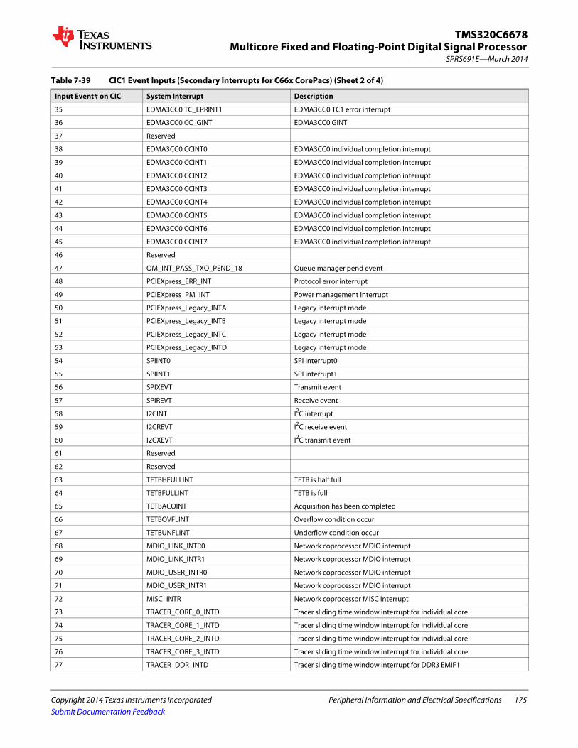
Multicore Fixed and Floating-Point Digital Signal Processor
Copyright 2014 Texas Instruments Incorporated Peripheral Information and Electrical Specifications 175
SPRS691E—March 2014
TMS320C6678
Submit Documentation Feedback
35 EDMA3CC0 TC_ERRINT1 EDMA3CC0 TC1 error interrupt
36 EDMA3CC0 CC_GINT EDMA3CC0 GINT
37 Reserved
38 EDMA3CC0 CCINT0 EDMA3CC0 individual completion interrupt
39 EDMA3CC0 CCINT1 EDMA3CC0 individual completion interrupt
40 EDMA3CC0 CCINT2 EDMA3CC0 individual completion interrupt
41 EDMA3CC0 CCINT3 EDMA3CC0 individual completion interrupt
42 EDMA3CC0 CCINT4 EDMA3CC0 individual completion interrupt
43 EDMA3CC0 CCINT5 EDMA3CC0 individual completion interrupt
44 EDMA3CC0 CCINT6 EDMA3CC0 individual completion interrupt
45 EDMA3CC0 CCINT7 EDMA3CC0 individual completion interrupt
46 Reserved
47 QM_INT_PASS_TXQ_PEND_18 Queue manager pend event
48 PCIEXpress_ERR_INT Protocol error interrupt
49 PCIEXpress_PM_INT Power management interrupt
50 PCIEXpress_Legacy_INTA Legacy interrupt mode
51 PCIEXpress_Legacy_INTB Legacy interrupt mode
52 PCIEXpress_Legacy_INTC Legacy interrupt mode
53 PCIEXpress_Legacy_INTD Legacy interrupt mode
54 SPIINT0 SPI interrupt0
55 SPIINT1 SPI interrupt1
56 SPIXEVT Transmit event
57 SPIREVT Receive event
58 I2CINT I2C interrupt
59 I2CREVT I2C receive event
60 I2CXEVT I2C transmit event
61 Reserved
62 Reserved
63 TETBHFULLINT TETB is half full
64 TETBFULLINT TETB is full
65 TETBACQINT Acquisition has been completed
66 TETBOVFLINT Overflow condition occur
67 TETBUNFLINT Underflow condition occur
68 MDIO_LINK_INTR0 Network coprocessor MDIO interrupt
69 MDIO_LINK_INTR1 Network coprocessor MDIO interrupt
70 MDIO_USER_INTR0 Network coprocessor MDIO interrupt
71 MDIO_USER_INTR1 Network coprocessor MDIO interrupt
72 MISC_INTR Network coprocessor MISC Interrupt
73 TRACER_CORE_0_INTD Tracer sliding time window interrupt for individual core
74 TRACER_CORE_1_INTD Tracer sliding time window interrupt for individual core
75 TRACER_CORE_2_INTD Tracer sliding time window interrupt for individual core
76 TRACER_CORE_3_INTD Tracer sliding time window interrupt for individual core
77 TRACER_DDR_INTD Tracer sliding time window interrupt for DDR3 EMIF1
Table 7-39 CIC1 Event Inputs (Secondary Interrupts for C66x CorePacs) (Sheet 2 of 4)
Input Event# on CIC System Interrupt Description

176 Peripheral Information and Electrical Specifications Copyright 2014 Texas Instruments Incorporated
SPRS691E—March 2014Multicore Fixed and Floating-Point Digital Signal ProcessorTMS320C6678
Submit Documentation Feedback
78 TRACER_MSMC_0_INTD Tracer sliding time window interrupt for MSMC SRAM bank0
79 TRACER_MSMC_1_INTD Tracer sliding time window interrupt for MSMC SRAM bank1
80 TRACER_MSMC_2_INTD Tracer sliding time window interrupt for MSMC SRAM bank2
81 TRACER_MSMC_3_INTD Tracer sliding time window interrupt for MSMC SRAM bank3
82 TRACER_CFG_INTD Tracer sliding time window interrupt for CFG0 TeraNet
83 TRACER_QM_CFG_INTD Tracer sliding time window interrupt for QM_SS CFG
84 TRACER_QM_DMA_INTD Tracer sliding time window interrupt for QM_SS slave
85 TRACER_SM_INTD Tracer sliding time window interrupt for semaphore
86 PSC_ALLINT Power/sleep controller interrupt
87 MSMC_SCRUB_CERROR Correctable (1-bit) soft error detected during scrub cycle
88 BOOTCFG_INTD BOOTCFG Interrupt BOOTCFG_ERR and BOOTCFG_PROT
89 Reserved
90 MPU0_INTD (MPU0_ADDR_ERR_INT and MPU0_PROT_ERR_INT combined)
MPU0 addressing violation interrupt and protection violation interrupt.
91 QM_INT_PASS_TXQ_PEND_19 Queue manager pend event
92 MPU1_INTD (MPU1_ADDR_ERR_INT and MPU1_PROT_ERR_INT combined)
MPU1 addressing violation interrupt and protection violation interrupt.
93 QM_INT_PASS_TXQ_PEND_20 Queue manager pend event
94 MPU2_INTD (MPU2_ADDR_ERR_INT and MPU2_PROT_ERR_INT combined)
MPU2 addressing violation interrupt and protection violation interrupt.
95 QM_INT_PASS_TXQ_PEND_21 Queue manager pend event
96 MPU3_INTD (MPU3_ADDR_ERR_INT and MPU3_PROT_ERR_INT combined)
MPU3 addressing violation interrupt and protection violation interrupt.
97 QM_INT_PASS_TXQ_PEND_22 Queue manager pend event
98 MSMC_dedc_cerror Correctable (1-bit) soft error detected on SRAM read
99 MSMC_dedc_nc_error Non-correctable (2-bit) soft error detected on SRAM read
100 MSMC_scrub_nc_error Non-correctable (2-bit) soft error detected during scrub cycle
101 Reserved
102 MSMC_mpf_error8 Memory protection fault indicators for each system master PrivID
103 MSMC_mpf_error9 Memory protection fault indicators for each system master PrivID
104 MSMC_mpf_error10 Memory protection fault indicators for each system master PrivID
105 MSMC_mpf_error11 Memory protection fault indicators for each system master PrivID
106 MSMC_mpf_error12 Memory protection fault indicators for each system master PrivID
107 MSMC_mpf_error13 Memory protection fault indicators for each system master PrivID
108 MSMC_mpf_error14 Memory protection fault indicators for each system master PrivID
109 MSMC_mpf_error15 Memory protection fault indicators for each system master PrivID
110 DDR3_ERR DDR3 EMIF error interrupt
111 VUSR_INT_O HyperLink interrupt
112 INTDST0 RapidIO interrupt
113 INTDST1 RapidIO interrupt
114 INTDST2 RapidIO interrupt
115 INTDST3 RapidIO interrupt
116 INTDST4 RapidIO interrupt
117 INTDST5 RapidIO interrupt
118 INTDST6 RapidIO interrupt
Table 7-39 CIC1 Event Inputs (Secondary Interrupts for C66x CorePacs) (Sheet 3 of 4)
Input Event# on CIC System Interrupt Description
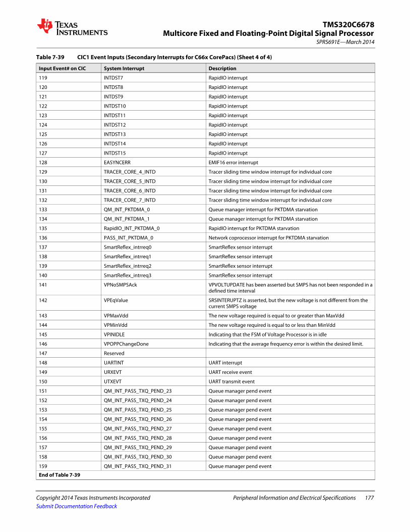
Multicore Fixed and Floating-Point Digital Signal Processor
Copyright 2014 Texas Instruments Incorporated Peripheral Information and Electrical Specifications 177
SPRS691E—March 2014
TMS320C6678
Submit Documentation Feedback
119 INTDST7 RapidIO interrupt
120 INTDST8 RapidIO interrupt
121 INTDST9 RapidIO interrupt
122 INTDST10 RapidIO interrupt
123 INTDST11 RapidIO interrupt
124 INTDST12 RapidIO interrupt
125 INTDST13 RapidIO interrupt
126 INTDST14 RapidIO interrupt
127 INTDST15 RapidIO interrupt
128 EASYNCERR EMIF16 error interrupt
129 TRACER_CORE_4_INTD Tracer sliding time window interrupt for individual core
130 TRACER_CORE_5_INTD Tracer sliding time window interrupt for individual core
131 TRACER_CORE_6_INTD Tracer sliding time window interrupt for individual core
132 TRACER_CORE_7_INTD Tracer sliding time window interrupt for individual core
133 QM_INT_PKTDMA_0 Queue manager interrupt for PKTDMA starvation
134 QM_INT_PKTDMA_1 Queue manager interrupt for PKTDMA starvation
135 RapidIO_INT_PKTDMA_0 RapidIO interrupt for PKTDMA starvation
136 PASS_INT_PKTDMA_0 Network coprocessor interrupt for PKTDMA starvation
137 SmartReflex_intrreq0 SmartReflex sensor interrupt
138 SmartReflex_intrreq1 SmartReflex sensor interrupt
139 SmartReflex_intrreq2 SmartReflex sensor interrupt
140 SmartReflex_intrreq3 SmartReflex sensor interrupt
141 VPNoSMPSAck VPVOLTUPDATE has been asserted but SMPS has not been responded in a defined time interval
142 VPEqValue SRSINTERUPTZ is asserted, but the new voltage is not different from the current SMPS voltage
143 VPMaxVdd The new voltage required is equal to or greater than MaxVdd
144 VPMinVdd The new voltage required is equal to or less than MinVdd
145 VPINIDLE Indicating that the FSM of Voltage Processor is in idle
146 VPOPPChangeDone Indicating that the average frequency error is within the desired limit.
147 Reserved
148 UARTINT UART interrupt
149 URXEVT UART receive event
150 UTXEVT UART transmit event
151 QM_INT_PASS_TXQ_PEND_23 Queue manager pend event
152 QM_INT_PASS_TXQ_PEND_24 Queue manager pend event
153 QM_INT_PASS_TXQ_PEND_25 Queue manager pend event
154 QM_INT_PASS_TXQ_PEND_26 Queue manager pend event
155 QM_INT_PASS_TXQ_PEND_27 Queue manager pend event
156 QM_INT_PASS_TXQ_PEND_28 Queue manager pend event
157 QM_INT_PASS_TXQ_PEND_29 Queue manager pend event
158 QM_INT_PASS_TXQ_PEND_30 Queue manager pend event
159 QM_INT_PASS_TXQ_PEND_31 Queue manager pend event
End of Table 7-39
Table 7-39 CIC1 Event Inputs (Secondary Interrupts for C66x CorePacs) (Sheet 4 of 4)
Input Event# on CIC System Interrupt Description
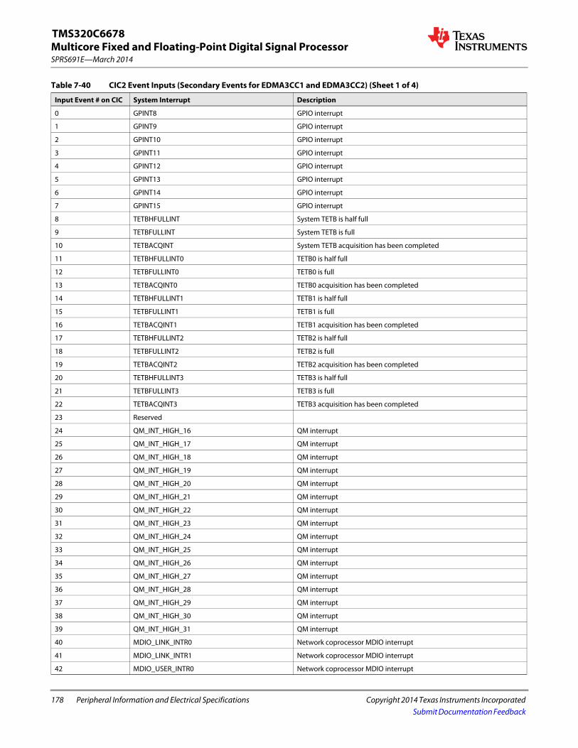
178 Peripheral Information and Electrical Specifications Copyright 2014 Texas Instruments Incorporated
SPRS691E—March 2014Multicore Fixed and Floating-Point Digital Signal ProcessorTMS320C6678
Submit Documentation Feedback
Table 7-40 CIC2 Event Inputs (Secondary Events for EDMA3CC1 and EDMA3CC2) (Sheet 1 of 4)
Input Event # on CIC System Interrupt Description
0 GPINT8 GPIO interrupt
1 GPINT9 GPIO interrupt
2 GPINT10 GPIO interrupt
3 GPINT11 GPIO interrupt
4 GPINT12 GPIO interrupt
5 GPINT13 GPIO interrupt
6 GPINT14 GPIO interrupt
7 GPINT15 GPIO interrupt
8 TETBHFULLINT System TETB is half full
9 TETBFULLINT System TETB is full
10 TETBACQINT System TETB acquisition has been completed
11 TETBHFULLINT0 TETB0 is half full
12 TETBFULLINT0 TETB0 is full
13 TETBACQINT0 TETB0 acquisition has been completed
14 TETBHFULLINT1 TETB1 is half full
15 TETBFULLINT1 TETB1 is full
16 TETBACQINT1 TETB1 acquisition has been completed
17 TETBHFULLINT2 TETB2 is half full
18 TETBFULLINT2 TETB2 is full
19 TETBACQINT2 TETB2 acquisition has been completed
20 TETBHFULLINT3 TETB3 is half full
21 TETBFULLINT3 TETB3 is full
22 TETBACQINT3 TETB3 acquisition has been completed
23 Reserved
24 QM_INT_HIGH_16 QM interrupt
25 QM_INT_HIGH_17 QM interrupt
26 QM_INT_HIGH_18 QM interrupt
27 QM_INT_HIGH_19 QM interrupt
28 QM_INT_HIGH_20 QM interrupt
29 QM_INT_HIGH_21 QM interrupt
30 QM_INT_HIGH_22 QM interrupt
31 QM_INT_HIGH_23 QM interrupt
32 QM_INT_HIGH_24 QM interrupt
33 QM_INT_HIGH_25 QM interrupt
34 QM_INT_HIGH_26 QM interrupt
35 QM_INT_HIGH_27 QM interrupt
36 QM_INT_HIGH_28 QM interrupt
37 QM_INT_HIGH_29 QM interrupt
38 QM_INT_HIGH_30 QM interrupt
39 QM_INT_HIGH_31 QM interrupt
40 MDIO_LINK_INTR0 Network coprocessor MDIO interrupt
41 MDIO_LINK_INTR1 Network coprocessor MDIO interrupt
42 MDIO_USER_INTR0 Network coprocessor MDIO interrupt

Multicore Fixed and Floating-Point Digital Signal Processor
Copyright 2014 Texas Instruments Incorporated Peripheral Information and Electrical Specifications 179
SPRS691E—March 2014
TMS320C6678
Submit Documentation Feedback
43 MDIO_USER_INTR0 Network coprocessor MDIO interrupt
44 MISC_INTR Network coprocessor MISC interrupt
45 TRACER_CORE_0_INTD Tracer sliding time window interrupt for individual core
46 TRACER_CORE_1_INTD Tracer sliding time window interrupt for individual core
47 TRACER_CORE_2_INTD Tracer sliding time window interrupt for individual core
48 TRACER_CORE_3_INTD Tracer sliding time window interrupt for individual core
49 TRACER_DDR_INTD Tracer sliding time window interrupt for DDR3 EMIF
50 TRACER_MSMC_0_INTD Tracer sliding time window interrupt for MSMC SRAM bank0
51 TRACER_MSMC_1_INTD Tracer sliding time window interrupt for MSMC SRAM bank1
52 TRACER_MSMC_2_INTD Tracer sliding time window interrupt for MSMC SRAM bank2
53 TRACER_MSMC_3_INTD Tracer sliding time window interrupt for MSMC SRAM bank3
54 TRACER_CFG_INTD Tracer sliding time window interrupt for CFG0 TeraNet
55 TRACER_QM_CFG_INTD Tracer sliding time window interrupt for QM_SS CFG
56 TRACER_QM_DMA_INTD Tracer sliding time window interrupt for QM_SS slave port
57 TRACER_SM_INTD Tracer sliding time window interrupt for semaphore
58 SEMERR0 Semaphore interrupt
59 SEMERR1 Semaphore interrupt
60 SEMERR2 Semaphore interrupt
61 SEMERR3 Semaphore interrupt
62 BOOTCFG_INTD BOOTCFG interrupt BOOTCFG_ERR and BOOTCFG_PROT
63 PASS_INT_PKTDMA_0 Network coprocessor interrupt for packet DMA starvation
64 MPU0_INTD (MPU0_ADDR_ERR_INT and MPU0_PROT_ERR_INT combined)
MPU0 addressing violation interrupt and protection violation interrupt.
65 MSMC_scrub_cerror Correctable (1-bit) soft error detected during scrub cycle
66 MPU1_INTD (MPU1_ADDR_ERR_INT and MPU1_PROT_ERR_INT combined)
MPU1 addressing violation interrupt and protection violation interrupt.
67 RapidIO_INT_PKTDMA_0 RapidIO interrupt for packet DMA starvation
68 MPU2_INTD (MPU2_ADDR_ERR_INT and MPU2_PROT_ERR_INT combined)
MPU2 addressing violation interrupt and protection violation interrupt.
69 QM_INT_PKTDMA_0 QM interrupt for packet DMA starvation
70 MPU3_INTD (MPU3_ADDR_ERR_INT and MPU3_PROT_ERR_INT combined)
MPU3 addressing violation interrupt and protection violation interrupt.
71 QM_INT_PKTDMA_1 QM interrupt for packet DMA starvation
72 MSMC_dedc_cerror Correctable (1-bit) soft error detected on SRAM read
73 MSMC_dedc_nc_error Non-correctable (2-bit) soft error detected on SRAM read
74 MSMC_scrub_nc_error Non-correctable (2-bit) soft error detected during scrub cycle
75 Reserved
76 MSMC_mpf_error0 Memory protection fault indicators for each system master PrivID
77 MSMC_mpf_error1 Memory protection fault indicators for each system master PrivID
78 MSMC_mpf_error2 Memory protection fault indicators for each system master PrivID
79 MSMC_mpf_error3 Memory protection fault indicators for each system master PrivID
80 MSMC_mpf_error4 Memory protection fault indicators for each system master PrivID
81 MSMC_mpf_error5 Memory protection fault indicators for each system master PrivID
82 MSMC_mpf_error6 Memory protection fault indicators for each system master PrivID
83 MSMC_mpf_error7 Memory protection fault indicators for each system master PrivID
Table 7-40 CIC2 Event Inputs (Secondary Events for EDMA3CC1 and EDMA3CC2) (Sheet 2 of 4)
Input Event # on CIC System Interrupt Description

180 Peripheral Information and Electrical Specifications Copyright 2014 Texas Instruments Incorporated
SPRS691E—March 2014Multicore Fixed and Floating-Point Digital Signal ProcessorTMS320C6678
Submit Documentation Feedback
84 MSMC_mpf_error8 Memory protection fault indicators for each system master PrivID
85 MSMC_mpf_error9 Memory protection fault indicators for each system master PrivID
86 MSMC_mpf_error10 Memory protection fault indicators for each system master PrivID
87 MSMC_mpf_error11 Memory protection fault indicators for each system master PrivID
88 MSMC_mpf_error12 Memory protection fault indicators for each system master PrivID
89 MSMC_mpf_error13 Memory protection fault indicators for each system master PrivID
90 MSMC_mpf_error14 Memory protection fault indicators for each system master PrivID
91 MSMC_mpf_error15 Memory protection fault indicators for each system master PrivID
92 Reserved
93 INTDST0 RapidIO interrupt
94 INTDST1 RapidIO interrupt
95 INTDST2 RapidIO interrupt
96 INTDST3 RapidIO interrupt
97 INTDST4 RapidIO interrupt
98 INTDST5 RapidIO interrupt
99 INTDST6 RapidIO interrupt
100 INTDST7 RapidIO interrupt
101 INTDST8 RapidIO interrupt
102 INTDST9 RapidIO interrupt
103 INTDST10 RapidIO interrupt
104 INTDST11 RapidIO interrupt
105 INTDST12 RapidIO interrupt
106 INTDST13 RapidIO interrupt
107 INTDST14 RapidIO interrupt
108 INTDST15 RapidIO interrupt
109 INTDST16 RapidIO interrupt
110 INTDST17 RapidIO interrupt
111 INTDST18 RapidIO interrupt
112 INTDST19 RapidIO interrupt
113 INTDST20 RapidIO interrupt
114 INTDST21 RapidIO interrupt
115 INTDST22 RapidIO interrupt
116 INTDST23 RapidIO interrupt
117 EASYNCERR EMIF16 error interrupt
118 TETBHFULLINT4 TETB4 is half full
119 TETBFULLINT4 TETB4 is full
120 TETBACQINT4 TETB4 acquisition has been completed
121 TETBHFULLINT5 TETB5 is half full
122 TETBFULLINT5 TETB5 is full
123 TETBACQINT5 TETB5 acquisition has been completed
124 TETBHFULLINT6 TETB6 is half full
125 TETBFULLINT6 TETB6 is full
126 TETBACQINT6 TETB6 acquisition has been completed
127 TETBHFULLINT7 TETB7 is half full
Table 7-40 CIC2 Event Inputs (Secondary Events for EDMA3CC1 and EDMA3CC2) (Sheet 3 of 4)
Input Event # on CIC System Interrupt Description
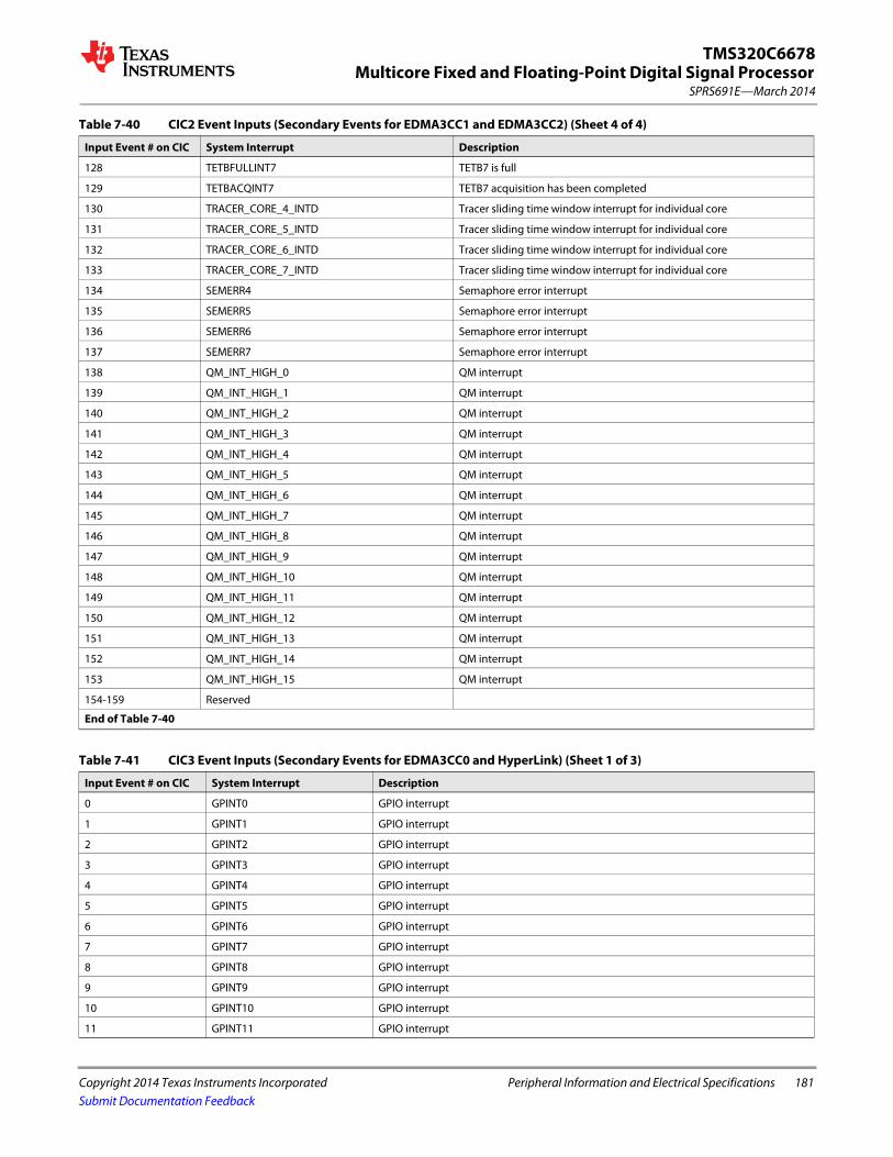
Multicore Fixed and Floating-Point Digital Signal Processor
Copyright 2014 Texas Instruments Incorporated Peripheral Information and Electrical Specifications 181
SPRS691E—March 2014
TMS320C6678
Submit Documentation Feedback
128 TETBFULLINT7 TETB7 is full
129 TETBACQINT7 TETB7 acquisition has been completed
130 TRACER_CORE_4_INTD Tracer sliding time window interrupt for individual core
131 TRACER_CORE_5_INTD Tracer sliding time window interrupt for individual core
132 TRACER_CORE_6_INTD Tracer sliding time window interrupt for individual core
133 TRACER_CORE_7_INTD Tracer sliding time window interrupt for individual core
134 SEMERR4 Semaphore error interrupt
135 SEMERR5 Semaphore error interrupt
136 SEMERR6 Semaphore error interrupt
137 SEMERR7 Semaphore error interrupt
138 QM_INT_HIGH_0 QM interrupt
139 QM_INT_HIGH_1 QM interrupt
140 QM_INT_HIGH_2 QM interrupt
141 QM_INT_HIGH_3 QM interrupt
142 QM_INT_HIGH_4 QM interrupt
143 QM_INT_HIGH_5 QM interrupt
144 QM_INT_HIGH_6 QM interrupt
145 QM_INT_HIGH_7 QM interrupt
146 QM_INT_HIGH_8 QM interrupt
147 QM_INT_HIGH_9 QM interrupt
148 QM_INT_HIGH_10 QM interrupt
149 QM_INT_HIGH_11 QM interrupt
150 QM_INT_HIGH_12 QM interrupt
151 QM_INT_HIGH_13 QM interrupt
152 QM_INT_HIGH_14 QM interrupt
153 QM_INT_HIGH_15 QM interrupt
154-159 Reserved
End of Table 7-40
Table 7-41 CIC3 Event Inputs (Secondary Events for EDMA3CC0 and HyperLink) (Sheet 1 of 3)
Input Event # on CIC System Interrupt Description
0 GPINT0 GPIO interrupt
1 GPINT1 GPIO interrupt
2 GPINT2 GPIO interrupt
3 GPINT3 GPIO interrupt
4 GPINT4 GPIO interrupt
5 GPINT5 GPIO interrupt
6 GPINT6 GPIO interrupt
7 GPINT7 GPIO interrupt
8 GPINT8 GPIO interrupt
9 GPINT9 GPIO interrupt
10 GPINT10 GPIO interrupt
11 GPINT11 GPIO interrupt
Table 7-40 CIC2 Event Inputs (Secondary Events for EDMA3CC1 and EDMA3CC2) (Sheet 4 of 4)
Input Event # on CIC System Interrupt Description
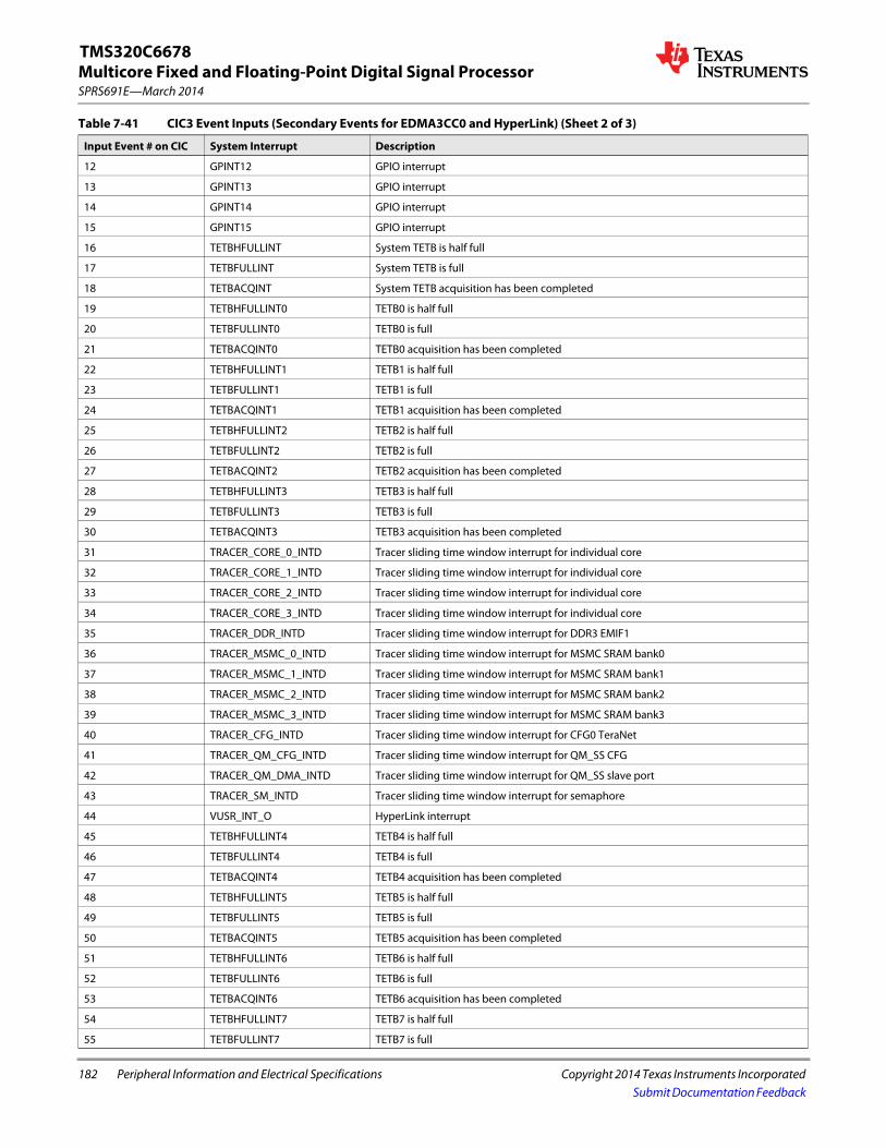
182 Peripheral Information and Electrical Specifications Copyright 2014 Texas Instruments Incorporated
SPRS691E—March 2014Multicore Fixed and Floating-Point Digital Signal ProcessorTMS320C6678
Submit Documentation Feedback
12 GPINT12 GPIO interrupt
13 GPINT13 GPIO interrupt
14 GPINT14 GPIO interrupt
15 GPINT15 GPIO interrupt
16 TETBHFULLINT System TETB is half full
17 TETBFULLINT System TETB is full
18 TETBACQINT System TETB acquisition has been completed
19 TETBHFULLINT0 TETB0 is half full
20 TETBFULLINT0 TETB0 is full
21 TETBACQINT0 TETB0 acquisition has been completed
22 TETBHFULLINT1 TETB1 is half full
23 TETBFULLINT1 TETB1 is full
24 TETBACQINT1 TETB1 acquisition has been completed
25 TETBHFULLINT2 TETB2 is half full
26 TETBFULLINT2 TETB2 is full
27 TETBACQINT2 TETB2 acquisition has been completed
28 TETBHFULLINT3 TETB3 is half full
29 TETBFULLINT3 TETB3 is full
30 TETBACQINT3 TETB3 acquisition has been completed
31 TRACER_CORE_0_INTD Tracer sliding time window interrupt for individual core
32 TRACER_CORE_1_INTD Tracer sliding time window interrupt for individual core
33 TRACER_CORE_2_INTD Tracer sliding time window interrupt for individual core
34 TRACER_CORE_3_INTD Tracer sliding time window interrupt for individual core
35 TRACER_DDR_INTD Tracer sliding time window interrupt for DDR3 EMIF1
36 TRACER_MSMC_0_INTD Tracer sliding time window interrupt for MSMC SRAM bank0
37 TRACER_MSMC_1_INTD Tracer sliding time window interrupt for MSMC SRAM bank1
38 TRACER_MSMC_2_INTD Tracer sliding time window interrupt for MSMC SRAM bank2
39 TRACER_MSMC_3_INTD Tracer sliding time window interrupt for MSMC SRAM bank3
40 TRACER_CFG_INTD Tracer sliding time window interrupt for CFG0 TeraNet
41 TRACER_QM_CFG_INTD Tracer sliding time window interrupt for QM_SS CFG
42 TRACER_QM_DMA_INTD Tracer sliding time window interrupt for QM_SS slave port
43 TRACER_SM_INTD Tracer sliding time window interrupt for semaphore
44 VUSR_INT_O HyperLink interrupt
45 TETBHFULLINT4 TETB4 is half full
46 TETBFULLINT4 TETB4 is full
47 TETBACQINT4 TETB4 acquisition has been completed
48 TETBHFULLINT5 TETB5 is half full
49 TETBFULLINT5 TETB5 is full
50 TETBACQINT5 TETB5 acquisition has been completed
51 TETBHFULLINT6 TETB6 is half full
52 TETBFULLINT6 TETB6 is full
53 TETBACQINT6 TETB6 acquisition has been completed
54 TETBHFULLINT7 TETB7 is half full
55 TETBFULLINT7 TETB7 is full
Table 7-41 CIC3 Event Inputs (Secondary Events for EDMA3CC0 and HyperLink) (Sheet 2 of 3)
Input Event # on CIC System Interrupt Description
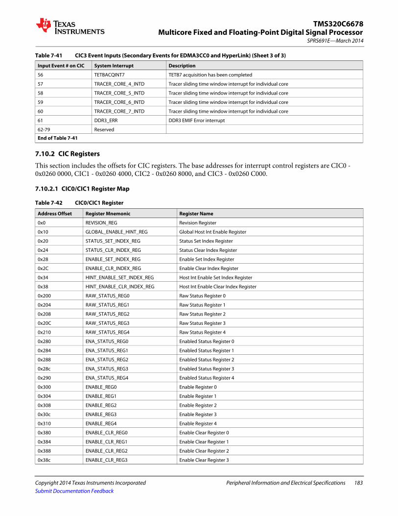
Multicore Fixed and Floating-Point Digital Signal Processor
Copyright 2014 Texas Instruments Incorporated Peripheral Information and Electrical Specifications 183
SPRS691E—March 2014
TMS320C6678
Submit Documentation Feedback
7.10.2 CIC Registers
This section includes the offsets for CIC registers. The base addresses for interrupt control registers are CIC0 - 0x0260 0000, CIC1 - 0x0260 4000, CIC2 - 0x0260 8000, and CIC3 - 0x0260 C000.
7.10.2.1 CIC0/CIC1 Register Map
56 TETBACQINT7 TETB7 acquisition has been completed
57 TRACER_CORE_4_INTD Tracer sliding time window interrupt for individual core
58 TRACER_CORE_5_INTD Tracer sliding time window interrupt for individual core
59 TRACER_CORE_6_INTD Tracer sliding time window interrupt for individual core
60 TRACER_CORE_7_INTD Tracer sliding time window interrupt for individual core
61 DDR3_ERR DDR3 EMIF Error interrupt
62-79 Reserved
End of Table 7-41
Table 7-42 CIC0/CIC1 Register
Address Offset Register Mnemonic Register Name
0x0 REVISION_REG Revision Register
0x10 GLOBAL_ENABLE_HINT_REG Global Host Int Enable Register
0x20 STATUS_SET_INDEX_REG Status Set Index Register
0x24 STATUS_CLR_INDEX_REG Status Clear Index Register
0x28 ENABLE_SET_INDEX_REG Enable Set Index Register
0x2C ENABLE_CLR_INDEX_REG Enable Clear Index Register
0x34 HINT_ENABLE_SET_INDEX_REG Host Int Enable Set Index Register
0x38 HINT_ENABLE_CLR_INDEX_REG Host Int Enable Clear Index Register
0x200 RAW_STATUS_REG0 Raw Status Register 0
0x204 RAW_STATUS_REG1 Raw Status Register 1
0x208 RAW_STATUS_REG2 Raw Status Register 2
0x20C RAW_STATUS_REG3 Raw Status Register 3
0x210 RAW_STATUS_REG4 Raw Status Register 4
0x280 ENA_STATUS_REG0 Enabled Status Register 0
0x284 ENA_STATUS_REG1 Enabled Status Register 1
0x288 ENA_STATUS_REG2 Enabled Status Register 2
0x28c ENA_STATUS_REG3 Enabled Status Register 3
0x290 ENA_STATUS_REG4 Enabled Status Register 4
0x300 ENABLE_REG0 Enable Register 0
0x304 ENABLE_REG1 Enable Register 1
0x308 ENABLE_REG2 Enable Register 2
0x30c ENABLE_REG3 Enable Register 3
0x310 ENABLE_REG4 Enable Register 4
0x380 ENABLE_CLR_REG0 Enable Clear Register 0
0x384 ENABLE_CLR_REG1 Enable Clear Register 1
0x388 ENABLE_CLR_REG2 Enable Clear Register 2
0x38c ENABLE_CLR_REG3 Enable Clear Register 3
Table 7-41 CIC3 Event Inputs (Secondary Events for EDMA3CC0 and HyperLink) (Sheet 3 of 3)
Input Event # on CIC System Interrupt Description

184 Peripheral Information and Electrical Specifications Copyright 2014 Texas Instruments Incorporated
SPRS691E—March 2014Multicore Fixed and Floating-Point Digital Signal ProcessorTMS320C6678
Submit Documentation Feedback
0x390 ENABLE_CLR_REG4 Enable Clear Register 4
0x400 CH_MAP_REG0 Interrupt Channel Map Register for 0 to 0+3
0x404 CH_MAP_REG1 Interrupt Channel Map Register for 4 to 4+3
0x408 CH_MAP_REG2 Interrupt Channel Map Register for 8 to 8+3
0x40c CH_MAP_REG3 Interrupt Channel Map Register for 12 to 12+3
0x410 CH_MAP_REG4 Interrupt Channel Map Register for 16 to 16+3
0x414 CH_MAP_REG5 Interrupt Channel Map Register for 20 to 20+3
0x418 CH_MAP_REG6 Interrupt Channel Map Register for 24 to 24+3
0x41c CH_MAP_REG7 Interrupt Channel Map Register for 28 to 28+3
0x420 CH_MAP_REG8 Interrupt Channel Map Register for 32 to 32+3
0x424 CH_MAP_REG9 Interrupt Channel Map Register for 36 to 36+3
0x428 CH_MAP_REG10 Interrupt Channel Map Register for 40 to 40+3
0x42c CH_MAP_REG11 Interrupt Channel Map Register for 44 to 44+3
0x430 CH_MAP_REG12 Interrupt Channel Map Register for 48 to 48+3
0x434 CH_MAP_REG13 Interrupt Channel Map Register for 52 to 52+3
0x438 CH_MAP_REG14 Interrupt Channel Map Register for 56 to 56+3
0x43c CH_MAP_REG15 Interrupt Channel Map Register for 60 to 60+3
0x440 CH_MAP_REG16 Interrupt Channel Map Register for 64 to 64+3
0x444 CH_MAP_REG17 Interrupt Channel Map Register for 68 to 68+3
0x448 CH_MAP_REG18 Interrupt Channel Map Register for 72 to 72+3
0x44c CH_MAP_REG19 Interrupt Channel Map Register for 76 to 76+3
0x450 CH_MAP_REG20 Interrupt Channel Map Register for 80 to 80+3
0x454 CH_MAP_REG21 Interrupt Channel Map Register for 84 to 84+3
0x458 CH_MAP_REG22 Interrupt Channel Map Register for 88 to 88+3
0x45c CH_MAP_REG23 Interrupt Channel Map Register for 92 to 92+3
0x460 CH_MAP_REG24 Interrupt Channel Map Register for 96 to 96+3
0x464 CH_MAP_REG25 Interrupt Channel Map Register for 100 to 100+3
0x468 CH_MAP_REG26 Interrupt Channel Map Register for 104 to 104+3
0x46c CH_MAP_REG27 Interrupt Channel Map Register for 108 to 108+3
0x470 CH_MAP_REG28 Interrupt Channel Map Register for 112 to 112+3
0x474 CH_MAP_REG29 Interrupt Channel Map Register for 116 to 116+3
0x478 CH_MAP_REG30 Interrupt Channel Map Register for 120 to 120+3
0x47c CH_MAP_REG31 Interrupt Channel Map Register for 124 to 124+3
0x480 CH_MAP_REG32 Interrupt Channel Map Register for 128 to 128+3
0x484 CH_MAP_REG33 Interrupt Channel Map Register for 132 to 132+3
0x488 CH_MAP_REG34 Interrupt Channel Map Register for 136 to 136+3
0x48c CH_MAP_REG35 Interrupt Channel Map Register for 140 to 140+3
0x490 CH_MAP_REG36 Interrupt Channel Map Register for 144 to 144+3
0x494 CH_MAP_REG37 Interrupt Channel Map Register for 148 to 148+3
0x498 CH_MAP_REG38 Interrupt Channel Map Register for 152 to 152+3
0x49c CH_MAP_REG39 Interrupt Channel Map Register for 156 to 156+3
0x800 HINT_MAP_REG0 Host Interrupt Map Register for 0 to 0+3
0x804 HINT_MAP_REG1 Host Interrupt Map Register for 4 to 4+3
Table 7-42 CIC0/CIC1 Register
Address Offset Register Mnemonic Register Name

Multicore Fixed and Floating-Point Digital Signal Processor
Copyright 2014 Texas Instruments Incorporated Peripheral Information and Electrical Specifications 185
SPRS691E—March 2014
TMS320C6678
Submit Documentation Feedback
7.10.2.2 CIC2 Register Map
0x808 HINT_MAP_REG2 Host Interrupt Map Register for 8 to 8+3
0x80c HINT_MAP_REG3 Host Interrupt Map Register for 12 to 12+3
0x810 HINT_MAP_REG4 Host Interrupt Map Register for 16 to 16+3
0x814 HINT_MAP_REG5 Host Interrupt Map Register for 20 to 20+3
0x818 HINT_MAP_REG6 Host Interrupt Map Register for 24 to 24+3
0x81c HINT_MAP_REG7 Host Interrupt Map Register for 28 to 28+3
0x820 HINT_MAP_REG8 Host Interrupt Map Register for 32 to 32+3
0x824 HINT_MAP_REG9 Host Interrupt Map Register for 36 to 36+3
0x828 HINT_MAP_REG10 Host Interrupt Map Register for 40 to 40+3
0x82c HINT_MAP_REG11 Host Interrupt Map Register for 44 to 44+3
0x830 HINT_MAP_REG12 Host Interrupt Map Register for 48 to 48+3
0x834 HINT_MAP_REG13 Host Interrupt Map Register for 52 to 52+3
0x838 HINT_MAP_REG14 Host Interrupt Map Register for 56 to 56+3
0x83c HINT_MAP_REG15 Host Interrupt Map Register for 60 to 60+3
0x840 HINT_MAP_REG16 Host Interrupt Map Register for 64 to 64+3
0x844 HINT_MAP_REG17 Host Interrupt Map Register for 68 to 68+3
0x848 HINT_MAP_REG18 Host Interrupt Map Register for 72 to 72+3
0x1500 ENABLE_HINT_REG0 Host Int Enable Register 0
0x1504 ENABLE_HINT_REG1 Host Int Enable Register 1
0x1508 ENABLE_HINT_REG2 Host Int Enable Register 2
End of Table 7-42
Table 7-43 CIC2 Register
Address Offset Register Mnemonic Register Name
0x0 REVISION_REG Revision Register
0x10 GLOBAL_ENABLE_HINT_REG Global Host Int Enable Register
0x20 STATUS_SET_INDEX_REG Status Set Index Register
0x24 STATUS_CLR_INDEX_REG Status Clear Index Register
0x28 ENABLE_SET_INDEX_REG Enable Set Index Register
0x2c ENABLE_CLR_INDEX_REG Enable Clear Index Register
0x34 HINT_ENABLE_SET_INDEX_REG Host Int Enable Set Index Register
0x38 HINT_ENABLE_CLR_INDEX_REG Host Int Enable Clear Index Register
0x200 RAW_STATUS_REG0 Raw Status Register 0
0x204 RAW_STATUS_REG1 Raw Status Register 1
0x208 RAW_STATUS_REG2 Raw Status Register 2
0x20c RAW_STATUS_REG3 Raw Status Register 3
0x210 RAW_STATUS_REG4 Raw Status Register 4
0x280 ENA_STATUS_REG0 Enabled Status Register 0
0x284 ENA_STATUS_REG1 Enabled Status Register 1
0x288 ENA_STATUS_REG2 Enabled Status Register 2
0x28c ENA_STATUS_REG3 Enabled Status Register 3
0x290 ENA_STATUS_REG4 Enabled Status Register 4
Table 7-42 CIC0/CIC1 Register
Address Offset Register Mnemonic Register Name
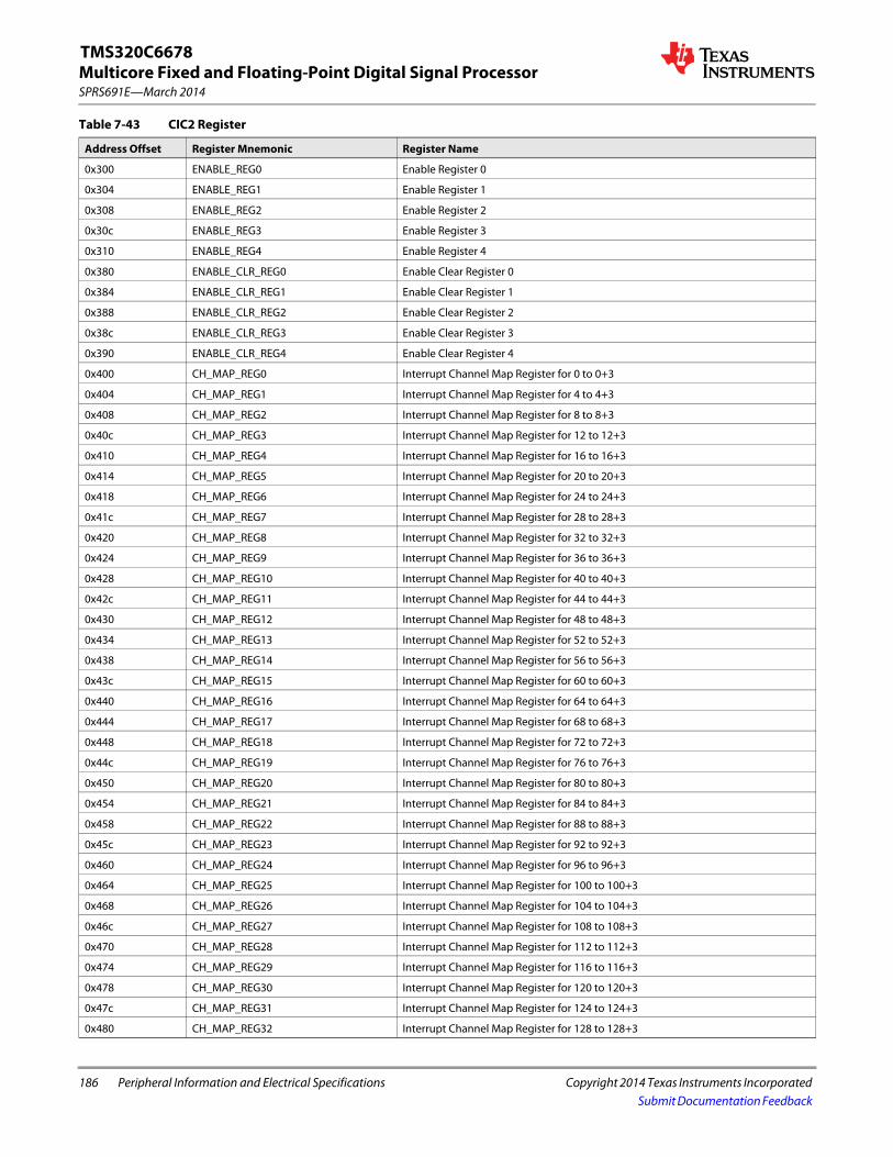
186 Peripheral Information and Electrical Specifications Copyright 2014 Texas Instruments Incorporated
SPRS691E—March 2014Multicore Fixed and Floating-Point Digital Signal ProcessorTMS320C6678
Submit Documentation Feedback
0x300 ENABLE_REG0 Enable Register 0
0x304 ENABLE_REG1 Enable Register 1
0x308 ENABLE_REG2 Enable Register 2
0x30c ENABLE_REG3 Enable Register 3
0x310 ENABLE_REG4 Enable Register 4
0x380 ENABLE_CLR_REG0 Enable Clear Register 0
0x384 ENABLE_CLR_REG1 Enable Clear Register 1
0x388 ENABLE_CLR_REG2 Enable Clear Register 2
0x38c ENABLE_CLR_REG3 Enable Clear Register 3
0x390 ENABLE_CLR_REG4 Enable Clear Register 4
0x400 CH_MAP_REG0 Interrupt Channel Map Register for 0 to 0+3
0x404 CH_MAP_REG1 Interrupt Channel Map Register for 4 to 4+3
0x408 CH_MAP_REG2 Interrupt Channel Map Register for 8 to 8+3
0x40c CH_MAP_REG3 Interrupt Channel Map Register for 12 to 12+3
0x410 CH_MAP_REG4 Interrupt Channel Map Register for 16 to 16+3
0x414 CH_MAP_REG5 Interrupt Channel Map Register for 20 to 20+3
0x418 CH_MAP_REG6 Interrupt Channel Map Register for 24 to 24+3
0x41c CH_MAP_REG7 Interrupt Channel Map Register for 28 to 28+3
0x420 CH_MAP_REG8 Interrupt Channel Map Register for 32 to 32+3
0x424 CH_MAP_REG9 Interrupt Channel Map Register for 36 to 36+3
0x428 CH_MAP_REG10 Interrupt Channel Map Register for 40 to 40+3
0x42c CH_MAP_REG11 Interrupt Channel Map Register for 44 to 44+3
0x430 CH_MAP_REG12 Interrupt Channel Map Register for 48 to 48+3
0x434 CH_MAP_REG13 Interrupt Channel Map Register for 52 to 52+3
0x438 CH_MAP_REG14 Interrupt Channel Map Register for 56 to 56+3
0x43c CH_MAP_REG15 Interrupt Channel Map Register for 60 to 60+3
0x440 CH_MAP_REG16 Interrupt Channel Map Register for 64 to 64+3
0x444 CH_MAP_REG17 Interrupt Channel Map Register for 68 to 68+3
0x448 CH_MAP_REG18 Interrupt Channel Map Register for 72 to 72+3
0x44c CH_MAP_REG19 Interrupt Channel Map Register for 76 to 76+3
0x450 CH_MAP_REG20 Interrupt Channel Map Register for 80 to 80+3
0x454 CH_MAP_REG21 Interrupt Channel Map Register for 84 to 84+3
0x458 CH_MAP_REG22 Interrupt Channel Map Register for 88 to 88+3
0x45c CH_MAP_REG23 Interrupt Channel Map Register for 92 to 92+3
0x460 CH_MAP_REG24 Interrupt Channel Map Register for 96 to 96+3
0x464 CH_MAP_REG25 Interrupt Channel Map Register for 100 to 100+3
0x468 CH_MAP_REG26 Interrupt Channel Map Register for 104 to 104+3
0x46c CH_MAP_REG27 Interrupt Channel Map Register for 108 to 108+3
0x470 CH_MAP_REG28 Interrupt Channel Map Register for 112 to 112+3
0x474 CH_MAP_REG29 Interrupt Channel Map Register for 116 to 116+3
0x478 CH_MAP_REG30 Interrupt Channel Map Register for 120 to 120+3
0x47c CH_MAP_REG31 Interrupt Channel Map Register for 124 to 124+3
0x480 CH_MAP_REG32 Interrupt Channel Map Register for 128 to 128+3
Table 7-43 CIC2 Register
Address Offset Register Mnemonic Register Name

Multicore Fixed and Floating-Point Digital Signal Processor
Copyright 2014 Texas Instruments Incorporated Peripheral Information and Electrical Specifications 187
SPRS691E—March 2014
TMS320C6678
Submit Documentation Feedback
7.10.2.3 CIC3 Register Map
0x484 CH_MAP_REG33 Interrupt Channel Map Register for 132 to 132+3
0x488 CH_MAP_REG34 Interrupt Channel Map Register for 136 to 136+3
0x48c CH_MAP_REG35 Interrupt Channel Map Register for 140 to 140+3
0x490 CH_MAP_REG36 Interrupt Channel Map Register for 144 to 144+3
0x494 CH_MAP_REG37 Interrupt Channel Map Register for 148 to 148+3
0x498 CH_MAP_REG38 Interrupt Channel Map Register for 152 to 152+3
0x49c CH_MAP_REG39 Interrupt Channel Map Register for 156 to 156+3
0x800 HINT_MAP_REG0 Host Interrupt Map Register for 0 to 0+3
0x804 HINT_MAP_REG1 Host Interrupt Map Register for 4 to 4+3
0x808 HINT_MAP_REG2 Host Interrupt Map Register for 8 to 8+3
0x80c HINT_MAP_REG3 Host Interrupt Map Register for 12 to 12+3
0x810 HINT_MAP_REG4 Host Interrupt Map Register for 16 to 16+3
0x814 HINT_MAP_REG5 Host Interrupt Map Register for 20 to 20+3
0x818 HINT_MAP_REG6 Host Interrupt Map Register for 24 to 24+3
0x81c HINT_MAP_REG7 Host Interrupt Map Register for 28 to 28+3
0x820 HINT_MAP_REG8 Host Interrupt Map Register for 32 to 32+3
0x824 HINT_MAP_REG9 Host Interrupt Map Register for 36 to 36+3
0x828 HINT_MAP_REG10 Host Interrupt Map Register for 40 to 40+3
0x82c HINT_MAP_REG11 Host Interrupt Map Register for 44 to 44+3
0x830 HINT_MAP_REG12 Host Interrupt Map Register for 48 to 48+3
0x1500 ENABLE_HINT_REG0 Host Int Enable Register 0
0x1504 ENABLE_HINT_REG1 Host Int Enable Register 1
End of Table 7-43
Table 7-44 CIC3 Register
Address Offset Register Mnemonic Register Name
0x0 REVISION_REG Revision Register
0x10 GLOBAL_ENABLE_HINT_REG Global Host Int Enable Register
0x20 STATUS_SET_INDEX_REG Status Set Index Register
0x24 STATUS_CLR_INDEX_REG Status Clear Index Register
0x28 ENABLE_SET_INDEX_REG Enable Set Index Register
0x2c ENABLE_CLR_INDEX_REG Enable Clear Index Register
0x34 HINT_ENABLE_SET_INDEX_REG Host Int Enable Set Index Register
0x38 HINT_ENABLE_CLR_INDEX_REG Host Int Enable Clear Index Register
0x200 RAW_STATUS_REG0 Raw Status Register 0
0x204 RAW_STATUS_REG1 Raw Status Register 1
0x280 ENA_STATUS_REG0 Enabled Status Register 0
0x284 ENA_STATUS_REG1 Enabled Status Register 1
0x300 ENABLE_REG0 Enable Register 0
0x304 ENABLE_REG1 Enable Register 1
0x380 ENABLE_CLR_REG0 Enable Clear Register 0
0x384 ENABLE_CLR_REG1 Enable Clear Register 1
Table 7-43 CIC2 Register
Address Offset Register Mnemonic Register Name

188 Peripheral Information and Electrical Specifications Copyright 2014 Texas Instruments Incorporated
SPRS691E—March 2014Multicore Fixed and Floating-Point Digital Signal ProcessorTMS320C6678
Submit Documentation Feedback
7.10.3 Inter-Processor Register Map
0x400 CH_MAP_REG0 Interrupt Channel Map Register for 0 to 0+3
0x404 CH_MAP_REG1 Interrupt Channel Map Register for 4 to 4+3
0x408 CH_MAP_REG2 Interrupt Channel Map Register for 8 to 8+3
0x40c CH_MAP_REG3 Interrupt Channel Map Register for 12 to 12+3
0x410 CH_MAP_REG4 Interrupt Channel Map Register for 16 to 16+3
0x414 CH_MAP_REG5 Interrupt Channel Map Register for 20 to 20+3
0x418 CH_MAP_REG6 Interrupt Channel Map Register for 24 to 24+3
0x41c CH_MAP_REG7 Interrupt Channel Map Register for 28 to 28+3
0x420 CH_MAP_REG8 Interrupt Channel Map Register for 32 to 32+3
0x424 CH_MAP_REG9 Interrupt Channel Map Register for 36 to 36+3
0x428 CH_MAP_REG10 Interrupt Channel Map Register for 40 to 40+3
0x42c CH_MAP_REG11 Interrupt Channel Map Register for 44 to 44+3
0x430 CH_MAP_REG12 Interrupt Channel Map Register for 48 to 48+3
0x434 CH_MAP_REG13 Interrupt Channel Map Register for 52 to 52+3
0x438 CH_MAP_REG14 Interrupt Channel Map Register for 56 to 56+3
0x43c CH_MAP_REG15 Interrupt Channel Map Register for 60 to 60+3
0x800 HINT_MAP_REG0 Host Interrupt Map Register for 0 to 0+3
0x804 HINT_MAP_REG1 Host Interrupt Map Register for 4 to 4+3
0x808 HINT_MAP_REG2 Host Interrupt Map Register for 8 to 8+3
0x80c HINT_MAP_REG3 Host Interrupt Map Register for 12 to 12+3
0x810 HINT_MAP_REG4 Host Interrupt Map Register for 16 to 16+3
0x814 HINT_MAP_REG5 Host Interrupt Map Register for 20 to 20+3
0x818 HINT_MAP_REG6 Host Interrupt Map Register for 24 to 24+3
0x81c HINT_MAP_REG7 Host Interrupt Map Register for 28 to 28+3
0x820 HINT_MAP_REG8 Host Interrupt Map Register for 32 to 32+3
0x824 HINT_MAP_REG9 Host Interrupt Map Register for 36 to 36+3
0x1500 ENABLE_HINT_REG0 Host Int Enable Register 0
0x1504 ENABLE_HINT_REG1 Host Int Enable Register 1
End of Table 7-44
Table 7-45 IPC Generation Registers (IPCGRx) (Sheet 1 of 2)
Address Start Address End Size Register Name Description
0x02620200 0x02620203 4B NMIGR0 NMI Event Generation Register for CorePac0
0x02620204 0x02620207 4B NMIGR1 NMI Event Generation Register for CorePac1
0x02620208 0x0262020B 4B NMIGR2 NMI Event Generation Register for CorePac2
0x0262020C 0x0262020F 4B NMIGR3 NMI Event Generation Register for CorePac3
0x02620210 0x02620213 4B NMIGR4 NMI Event Generation Register for CorePac4
0x02620214 0x02620217 4B NMIGR5 NMI Event Generation Register for CorePac5
0x02620218 0x0262021B 4B NMIGR6 NMI Event Generation Register for CorePac6
0x0262021C 0x0262021F 4B NMIGR7 NMI Event Generation Register for CorePac7
0x02620220 0x0262023F 32B Reserved Reserved
0x02620240 0x02620243 4B IPCGR0 IPC Generation Register for CorePac0
Table 7-44 CIC3 Register
Address Offset Register Mnemonic Register Name
Multicore Fixed and Floating-Point Digital Signal Processor
Copyright 2014 Texas Instruments Incorporated Peripheral Information and Electrical Specifications 189
SPRS691E—March 2014
TMS320C6678
Submit Documentation Feedback
7.10.4 NMI and LRESET
Non-maskable interrupts (NMI) can be generated by chip-level registers and the LRESET can be generated by software writing into LPSC registers. LRESET and NMI can also be asserted by device pins or watchdog timers. One NMI pin and one LRESET pin are shared by all CorePacs on the device. The CORESEL[3:0] pins can be configured to select between the CorePacs available as shown in Table 7-46.
0x02620244 0x02620247 4B IPCGR1 IPC Generation Register for CorePac1
0x02620248 0x0262024B 4B IPCGR2 IPC Generation Register for CorePac2
0x0262024C 0x0262024F 4B IPCGR3 IPC Generation Register for CorePac3
0x02620250 0x02620253 4B IPCGR4 IPC Generation Register for CorePac4
0x02620254 0x02620257 4B IPCGR5 IPC Generation Register for CorePac5
0x02620258 0x0262025B 4B IPCGR6 IPC Generation Register for CorePac6
0x0262025C 0x0262025F 4B IPCGR7 IPC Generation Register for CorePac7
0x02620260 0x0262027B 28B Reserved Reserved
0x0262027C 0x0262027F 4B IPCGRH IPC Generation Register for Host
0x02620280 0x02620283 4B IPCAR0 IPC Acknowledgement Register for CorePac0
0x02620284 0x02620287 4B IPCAR1 IPC Acknowledgement Register for CorePac1
0x02620288 0x0262028B 4B IPCAR2 IPC Acknowledgement Register for CorePac2
0x0262028C 0x0262028F 4B IPCAR3 IPC Acknowledgement Register for CorePac3
0x02620290 0x02620293 4B IPCAR4 IPC Acknowledgement Register for CorePac4
0x02620294 0x02620297 4B IPCAR5 IPC Acknowledgement Register for CorePac5
0x02620298 0x0262029B 4B IPCAR6 IPC Acknowledgement Register for CorePac6
0x0262029C 0x0262029F 4B IPCAR7 IPC Acknowledgement Register for CorePac7
0x026202A0 0x026202BB 28B Reserved Reserved
0x026202BC 0x026202BF 4B IPCARH IPC Acknowledgement Register for Host
End of Table 7-45
Table 7-46 LRESET and NMI Decoding (Sheet 1 of 2)
CORESEL[3:0] Pin Input LRESET Pin Input NMI Pin Input LRESETNMIEN Pin Input Reset Mux Block Output
XXXX X X 1 No local reset or NMI assertion.
0000 0 X 0 Assert local reset to CorePac0
0001 0 X 0 Assert local reset to CorePac1
0010 0 X 0 Assert local reset to CorePac2
0011 0 X 0 Assert local reset to CorePac3
0100 0 X 0 Assert local reset to CorePac4
0101 0 X 0 Assert local reset to CorePac5
0110 0 X 0 Assert local reset to CorePac6
0111 0 X 0 Assert local reset to CorePac7
1xxx 0 X 0 Assert local reset to all CorePacs
0000 1 1 0 De-assert local reset & NMI to CorePac0
0001 1 1 0 De-assert local reset & NMI to CorePac1
0010 1 1 0 De-assert local reset & NMI to CorePac2
0011 1 1 0 De-assert local reset & NMI to CorePac3
Table 7-45 IPC Generation Registers (IPCGRx) (Sheet 2 of 2)
Address Start Address End Size Register Name Description

190 Peripheral Information and Electrical Specifications Copyright 2014 Texas Instruments Incorporated
SPRS691E—March 2014Multicore Fixed and Floating-Point Digital Signal ProcessorTMS320C6678
Submit Documentation Feedback
7.10.5 External Interrupts Electrical Data/Timing
Figure 7-33 NMI and Local Reset Timing
0100 1 1 0 De-assert local reset & NMI to CorePac4
0101 1 1 0 De-assert local reset & NMI to CorePac5
0110 1 1 0 De-assert local reset & NMI to CorePac6
0111 1 1 0 De-assert local reset & NMI to CorePac7
1xxx 1 1 0 De-assert local reset & NMI to all CorePacs
0000 1 0 0 Assert NMI to CorePac0
0001 1 0 0 Assert NMI to CorePac1
0010 1 0 0 Assert NMI to CorePac2
0011 1 0 0 Assert NMI to CorePac3
0100 1 0 0 Assert NMI to CorePac4
0101 1 0 0 Assert NMI to CorePac5
0110 1 0 0 Assert NMI to CorePac6
0111 1 0 0 Assert NMI to CorePac7
1xxx 1 0 0 Assert NMI to all CorePacs
End of Table 7-46
Table 7-47 NMI and Local Reset Timing Requirements (1) (see Figure 7-33)
1 P = 1/SYSCLK1 frequency in ns.
No. Min Max Unit
1 tsu(LRESET-LRESETNMIENL) Setup Time - LRESET valid before LRESETNMIEN low 12*P ns
1 tsu(NMI-LRESETNMIENL) Setup Time - NMI valid before LRESETNMIEN low 12*P ns
1 tsu(CORESELn-LRESETNMIENL) Setup Time - CORESEL[2:0] valid before LRESETNMIEN low 12*P ns
2 th(LRESETNMIENL-LRESET) Hold Time - LRESET valid after LRESETNMIEN high 12*P ns
2 th(LRESETNMIENL-NMI) Hold Time - NMI valid after LRESETNMIEN high 12*P ns
2 th(LRESETNMIENL-CORESELn) Hold Time - CORESEL[2:0] valid after LRESETNMIEN high 12*P ns
3 tw(LRESETNMIEN) Pulse Width - LRESETNMIEN low width 12*P ns
End of Table 7-47
Table 7-46 LRESET and NMI Decoding (Sheet 2 of 2)
CORESEL[3:0] Pin Input LRESET Pin Input NMI Pin Input LRESETNMIEN Pin Input Reset Mux Block Output
3
LRESETNMIEN
CORESEL[3:0]//LRESET
NMI
1 2
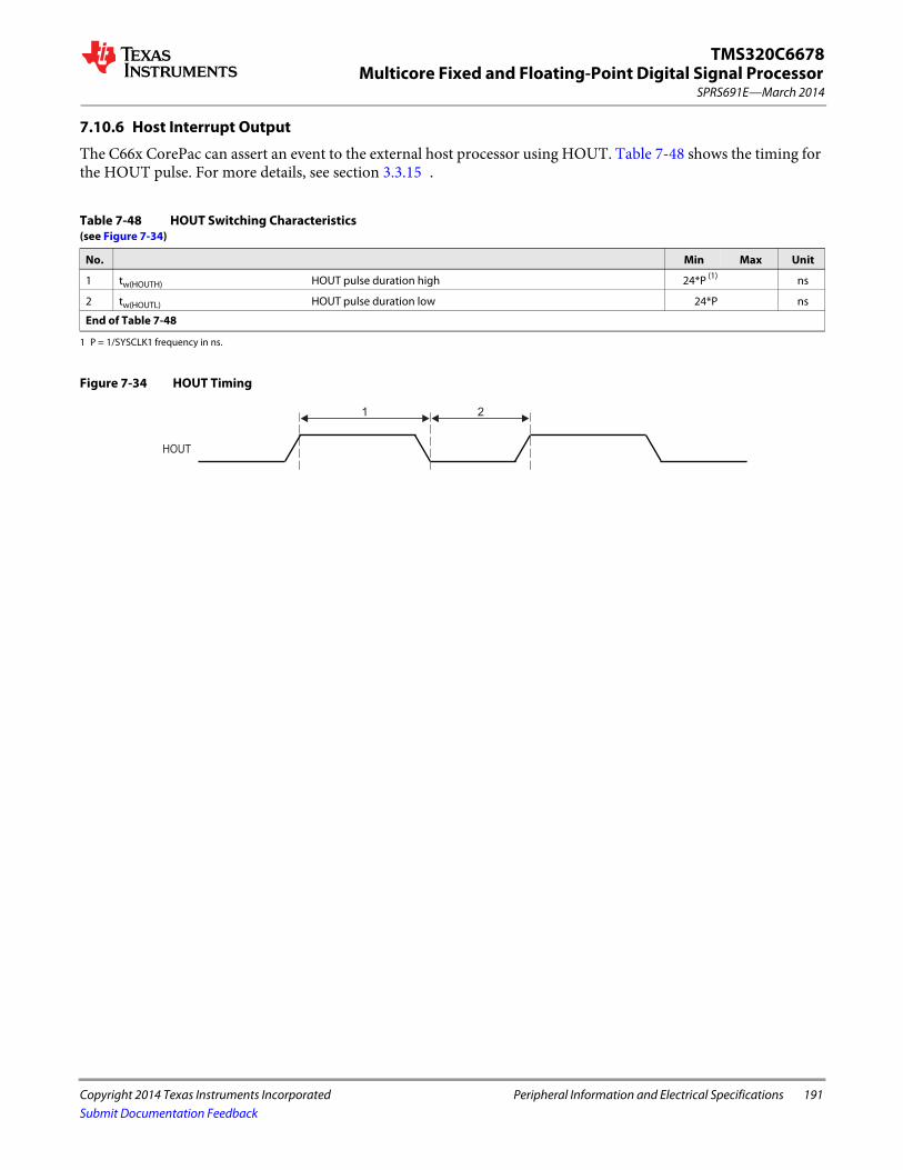
Multicore Fixed and Floating-Point Digital Signal Processor
Copyright 2014 Texas Instruments Incorporated Peripheral Information and Electrical Specifications 191
SPRS691E—March 2014
TMS320C6678
Submit Documentation Feedback
7.10.6 Host Interrupt Output
The C66x CorePac can assert an event to the external host processor using HOUT. Table 7-48 shows the timing for the HOUT pulse. For more details, see section 3.3.15 .
Figure 7-34 HOUT Timing
Table 7-48 HOUT Switching Characteristics (see Figure 7-34)
No. Min Max Unit
1 tw(HOUTH) HOUT pulse duration high 24*P (1)
1 P = 1/SYSCLK1 frequency in ns.
ns
2 tw(HOUTL) HOUT pulse duration low 24*P ns
End of Table 7-48
HOUT
21

192 Peripheral Information and Electrical Specifications Copyright 2014 Texas Instruments Incorporated
SPRS691E—March 2014Multicore Fixed and Floating-Point Digital Signal ProcessorTMS320C6678
Submit Documentation Feedback
7.11 Memory Protection Unit (MPU)The C6678 supports four MPUs:
• One MPU is used to protect the main CORE/3 CFG TeraNet (the CFG space of all slave devices on the TeraNet is protected by the MPU).
• Two MPUs are used for QM_SS (one for the DATA PORT port and one for the CFG PORT port).• One MPU is used for Semaphore.
This section contains MPU register map and details of device-specific MPU registers only. For MPU features and details of generic MPU registers, see the Memory Protection Unit (MPU) for KeyStone Devices User Guide in ‘‘Related Documentation from Texas Instruments’’ on page 72.
The following tables show the configuration of each MPU and the memory regions protected by each MPU.
Table 7-51 shows the privilege ID of each CORE and every mastering peripheral. Table 7-51 also shows the privilege level (supervisor vs. user), security level (secure vs. non-secure), and access type (instruction read vs. data/DMA read or write) of each master on the device. In some cases, a particular setting depends on software being executed at the time of the access or the configuration of the master peripheral.
Table 7-49 MPU Default Configuration
SettingMPU0(Main CFG TeraNet)
MPU1(QM_SS DATA PORT)
MPU2(QM_SS CFG PORT)
MPU3(Semaphore)
Default permission Assume allowed Assume allowed Assume allowed Assume allowed
Number of allowed IDs supported 16 16 16 16
Number of programmable ranges supported 16 5 16 1
Compare width 1KB granularity 1KB granularity 1KB granularity 1KB granularity
End of Table 7-49
Table 7-50 MPU Memory Regions
Memory Protection Start Address End Address
MPU0 Main CFG TeraNet 0x01D00000 0x026207FF
MPU1 QM_SS DATA PORT 0x34000000 0x340BFFFF
MPU2 QM_SS CFG PORT 0x02A00000 0x02ABFFFF
MPU3 Semaphore 0x02640000 0x026407FF
Table 7-51 Privilege ID Settings (Sheet 1 of 2)
Privilege ID Master Privilege Level Security Level Access Type
0 CorePac0 SW dependant, driven by MSMC SW dependant DMA
1 CorePac1 SW dependant, driven by MSMC SW dependant DMA
2 CorePac2 SW dependant, driven by MSMC SW dependant DMA
3 CorePac3 SW dependant, driven by MSMC SW dependant DMA
4 CorePac4 SW dependant, driven by MSMC SW dependant DMA
5 CorePac5 SW dependant, driven by MSMC SW dependant DMA
6 CorePac6 SW dependant, driven by MSMC SW dependant DMA
7 CorePac7 SW dependant, driven by MSMC SW dependant DMA
8 Network Coprocessor Packet DMA
User Non-secure DMA

Multicore Fixed and Floating-Point Digital Signal Processor
Copyright 2014 Texas Instruments Incorporated Peripheral Information and Electrical Specifications 193
SPRS691E—March 2014
TMS320C6678
Submit Documentation Feedback
Table 7-52 shows the master ID of each CorePac and every mastering peripheral. Master IDs are used to determine allowed connections between masters and slaves. Unlike privilege IDs, which can be shared across different masters, master IDs are unique to each master.
9 SRIO Packet DMA/SRIO_M User/Driven by SRIO block, User mode and supervisor mode is determined on a per-transaction basis. Only the transaction with source ID matching the value in the SupervisorID register is granted supervisor mode.
Non-secure DMA
10 QM_SS Packet DMA/QM_SS Second
User Non-secure DMA
11 PCIe Driven by PCIe module Non-secure DMA
12 Debug_SS Driven by Debug_SS Driven by Debug_SS DMA
13 HyperLink Driven by HyperLink Non-secure DMA
14 HyperLink Supervisor Non-secure DMA
15 TSIP0/1 User Non-secure DMA
End of Table 7-51
Table 7-52 Master ID Settings (Sheet 1 of 3) (1)
Master ID Master
0 CorePac0
1 CorePac1
2 CorePac2
3 CorePac3
4 CorePac4
5 CorePac5
6 CorePac6
7 CorePac7
8 CorePac0_CFG
9 CorePac1_CFG
10 CorePac2_CFG
11 CorePac3_CFG
12 CorePac4_CFG
13 CorePac5_CFG
14 CorePac6_CFG
15 CorePac7_CFG
16 EDMA0_TC0 read
17 EDMA0_TC0 write
18 EDMA0_TC1 read
19 EDMA0_TC1 write
20 EDMA1_TC0 read
21 EDMA1_TC0 write
22 EDMA1_TC1 read
23 EDMA1_TC1 write
24 EDMA1_TC2 read
25 EDMA1_TC2 write
Table 7-51 Privilege ID Settings (Sheet 2 of 2)
Privilege ID Master Privilege Level Security Level Access Type

194 Peripheral Information and Electrical Specifications Copyright 2014 Texas Instruments Incorporated
SPRS691E—March 2014Multicore Fixed and Floating-Point Digital Signal ProcessorTMS320C6678
Submit Documentation Feedback
26 EDMA1_TC3 read
27 EDMA1_TC3 write
28 EDMA2_TC0 read
29 EDMA2_TC0 write
30 EDMA2_TC1 read
31 EDMA2_TC1 write
32 EDMA2_TC2 read
33 EDMA2_TC2 write
34 EDMA2_TC3 read
35 EDMA2_TC3 write
36 - 37 Reserved
38 - 39 SRIO Packet DMA
40 - 47 Reserved
48 Debug SS
49 EDMA3CC0
50 EDMA3CC1
51 EDMA3CC2
52 MSMC (2)
53 PCIe
54 SRIO_Master
55 HyperLink
56 - 59 Network Coprocessor Packet DMA
60 - 85 Reserved
86 TSIP0
87 TSIP1
88 - 91 Queue Manager Packet DMA
92 - 93 Queue Manager Second
94 - 127 Reserved
128 Tracer_core_0 (3)
129 Tracer_core_1
130 Tracer_core_2
131 Tracer_core_3
132 Tracer_core_4
133 Tracer_core_5
134 Tracer_core_6
135 Tracer_core_7
136 Tracer_MSMC0
137 Tracer_MSMC1
138 Tracer_MSMC2
139 Tracer_MSMC3
140 Tracer_DDR
141 Tracer_SM
142 Tracer_QM_CFG
Table 7-52 Master ID Settings (Sheet 2 of 3) (1)
Master ID Master

Multicore Fixed and Floating-Point Digital Signal Processor
Copyright 2014 Texas Instruments Incorporated Peripheral Information and Electrical Specifications 195
SPRS691E—March 2014
TMS320C6678
Submit Documentation Feedback
7.11.1 MPU Registers
This section includes the offsets for MPU registers and definitions for device-specific MPU registers.
7.11.1.1 MPU Register Map
143 Tracer_QM_DMA
144 Tracer_CFG
End of Table 7-52
1 Some of the Packet DMA-based peripherals require multiple master IDs. Queue Manager Packet DMA is assigned with 88, 89, 90, 91, but only 88 - 89 are actually used. For the network coprocessor packet DMA port, 56, 57, 58, and 59 are assigned, while only one (56) is actually used. There are two master ID values assigned for the queue manager second master port: one master ID for external linking RAM and the other master ID for PDSP/MCDM accesses.
2 The master ID for MSMC is for the transactions initiated by MSMC internally and sent to the DDR.3 All traces are set to the same master ID and bit 7 of the master ID must be 1.
Table 7-53 MPU0 Registers (Sheet 1 of 2)
Offset Name Description
0h REVID Revision ID
4h CONFIG Configuration
10h IRAWSTAT Interrupt raw status/set
14h IENSTAT Interrupt enable status/clear
18h IENSET Interrupt enable
1Ch IENCLR Interrupt enable clear
20h EOI End of interrupt
200h PROG0_MPSAR Programmable range 0, start address
204h PROG0_MPEAR Programmable range 0, end address
208h PROG0_MPPA Programmable range 0, memory page protection attributes
210h PROG1_MPSAR Programmable range 1, start address
214h PROG1_MPEAR Programmable range 1, end address
218h PROG1_MPPA Programmable range 1, memory page protection attributes
220h PROG2_MPSAR Programmable range 2, start address
224h PROG2_MPEAR Programmable range 2, end address
228h PROG2_MPPA Programmable range 2, memory page protection attributes
230h PROG3_MPSAR Programmable range 3, start address
234h PROG3_MPEAR Programmable range 3, end address
238h PROG3_MPPA Programmable range 3, memory page protection attributes
240h PROG4_MPSAR Programmable range 4, start address
244h PROG4_MPEAR Programmable range 4, end address
248h PROG4_MPPA Programmable range 4, memory page protection attributes
250h PROG5_MPSAR Programmable range 5, start address
254h PROG5_MPEAR Programmable range 5, end address
258h PROG5_MPPA Programmable range 5, memory page protection attributes
260h PROG6_MPSAR Programmable range 6, start address
264h PROG6_MPEAR Programmable range 6, end address
268h PROG6_MPPA Programmable range 6, memory page protection attributes
270h PROG7_MPSAR Programmable range 7, start address
Table 7-52 Master ID Settings (Sheet 3 of 3) (1)
Master ID Master

196 Peripheral Information and Electrical Specifications Copyright 2014 Texas Instruments Incorporated
SPRS691E—March 2014Multicore Fixed and Floating-Point Digital Signal ProcessorTMS320C6678
Submit Documentation Feedback
274h PROG7_MPEAR Programmable range 7, end address
278h PROG7_MPPA Programmable range 7, memory page protection attributes
280h PROG8_MPSAR Programmable range 8, start address
284h PROG8_MPEAR Programmable range 8, end address
288h PROG8_MPPA Programmable range 8, memory page protection attributes
290h PROG9_MPSAR Programmable range 9, start address
294h PROG9_MPEAR Programmable range 9, end address
298h PROG9_MPPA Programmable range 9, memory page protection attributes
2A0h PROG10_MPSAR Programmable range 10, start address
2A4h PROG10_MPEAR Programmable range 10, end address
2A8h PROG10_MPPA Programmable range 10, memory page protection attributes
2B0h PROG11_MPSAR Programmable range 11, start address
2B4h PROG11_MPEAR Programmable range 11, end address
2B8h PROG11_MPPA Programmable range 11, memory page protection attributes
2C0h PROG12_MPSAR Programmable range 12, start address
2C4h PROG12_MPEAR Programmable range 12, end address
2C8h PROG12_MPPA Programmable range 12, memory page protection attributes
2D0h PROG13_MPSAR Programmable range 13, start address
2D4h PROG13_MPEAR Programmable range 13, end address
2Dh PROG13_MPPA Programmable range 13, memory page protection attributes
2E0h PROG14_MPSAR Programmable range 14, start address
2E4h PROG14_MPEAR Programmable range 14, end address
2E8h PROG14_MPPA Programmable range 14, memory page protection attributes
2F0h PROG15_MPSAR Programmable range 15, start address
2F4h PROG15_MPEAR Programmable range 15, end address
2F8h PROG15_MPPA Programmable range 15, memory page protection attributes
300h FLTADDRR Fault address
304h FLTSTAT Fault status
308h FLTCLR Fault clear
End of Table 7-53
Table 7-54 MPU1 Registers (Sheet 1 of 2)
Offset Name Description
0h REVID Revision ID
4h CONFIG Configuration
10h IRAWSTAT Interrupt raw status/set
14h IENSTAT Interrupt enable status/clear
18h IENSET Interrupt enable
1Ch IENCLR Interrupt enable clear
20h EOI End of interrupt
200h PROG0_MPSAR Programmable range 0, start address
204h PROG0_MPEAR Programmable range 0, end address
208h PROG0_MPPA Programmable range 0, memory page protection attributes
Table 7-53 MPU0 Registers (Sheet 2 of 2)
Offset Name Description

Multicore Fixed and Floating-Point Digital Signal Processor
Copyright 2014 Texas Instruments Incorporated Peripheral Information and Electrical Specifications 197
SPRS691E—March 2014
TMS320C6678
Submit Documentation Feedback
210h PROG1_MPSAR Programmable range 1, start address
214h PROG1_MPEAR Programmable range 1, end address
218h PROG1_MPPA Programmable range 1, memory page protection attributes
220h PROG2_MPSAR Programmable range 2, start address
224h PROG2_MPEAR Programmable range 2, end address
228h PROG2_MPPA Programmable range 2, memory page protection attributes
230h PROG3_MPSAR Programmable range 3, start address
234h PROG3_MPEAR Programmable range 3, end address
238h PROG3_MPPA Programmable range 3, memory page protection attributes
240h PROG4_MPSAR Programmable range 4, start address
244h PROG4_MPEAR Programmable range 4, end address
248h PROG4_MPPA Programmable range 4, memory page protection attributes
300h FLTADDRR Fault address
304h FLTSTAT Fault status
308h FLTCLR Fault clear
End of Table 7-54
Table 7-55 MPU2 Registers (Sheet 1 of 2)
Offset Name Description
0h REVID Revision ID
4h CONFIG Configuration
10h IRAWSTAT Interrupt raw status/set
14h IENSTAT Interrupt enable status/clear
18h IENSET Interrupt enable
1Ch IENCLR Interrupt enable clear
20h EOI End of interrupt
200h PROG0_MPSAR Programmable range 0, start address
204h PROG0_MPEAR Programmable range 0, end address
208h PROG0_MPPA Programmable range 0, memory page protection attributes
210h PROG1_MPSAR Programmable range 1, start address
214h PROG1_MPEAR Programmable range 1, end address
218h PROG1_MPPA Programmable range 1, memory page protection attributes
220h PROG2_MPSAR Programmable range 2, start address
224h PROG2_MPEAR Programmable range 2, end address
228h PROG2_MPPA Programmable range 2, memory page protection attributes
230h PROG3_MPSAR Programmable range 3, start address
234h PROG3_MPEAR Programmable range 3, end address
238h PROG3_MPPA Programmable range 3, memory page protection attributes
240h PROG4_MPSAR Programmable range 4, start address
244h PROG4_MPEAR Programmable range 4, end address
248h PROG4_MPPA Programmable range 4, memory page protection attributes
250h PROG5_MPSAR Programmable range 5, start address
254h PROG5_MPEAR Programmable range 5, end address
Table 7-54 MPU1 Registers (Sheet 2 of 2)
Offset Name Description

198 Peripheral Information and Electrical Specifications Copyright 2014 Texas Instruments Incorporated
SPRS691E—March 2014Multicore Fixed and Floating-Point Digital Signal ProcessorTMS320C6678
Submit Documentation Feedback
258h PROG5_MPPA Programmable range 5, memory page protection attributes
260h PROG6_MPSAR Programmable range 6, start address
264h PROG6_MPEAR Programmable range 6, end address
268h PROG6_MPPA Programmable range 6, memory page protection attributes
270h PROG7_MPSAR Programmable range 7, start address
274h PROG7_MPEAR Programmable range 7, end address
278h PROG7_MPPA Programmable range 7, memory page protection attributes
280h PROG8_MPSAR Programmable range 8, start address
284h PROG8_MPEAR Programmable range 8, end address
288h PROG8_MPPA Programmable range 8, memory page protection attributes
290h PROG9_MPSAR Programmable range 9, start address
294h PROG9_MPEAR Programmable range 9, end address
298h PROG9_MPPA Programmable range 9, memory page protection attributes
2A0h PROG10_MPSAR Programmable range 10, start address
2A4h PROG10_MPEAR Programmable range 10, end address
2A8h PROG10_MPPA Programmable range 10, memory page protection attributes
2B0h PROG11_MPSAR Programmable range 11, start address
2B4h PROG11_MPEAR Programmable range 11, end address
2B8h PROG11_MPPA Programmable range 11, memory page protection attributes
2C0h PROG12_MPSAR Programmable range 12, start address
2C4h PROG12_MPEAR Programmable range 12, end address
2C8h PROG12_MPPA Programmable range 12, memory page protection attributes
2D0h PROG13_MPSAR Programmable range 13, start address
2D4h PROG13_MPEAR Programmable range 13, end address
2Dh PROG13_MPPA Programmable range 13, memory page protection attributes
2E0h PROG14_MPSAR Programmable range 14, start address
2E4h PROG14_MPEAR Programmable range 14, end address
2E8h PROG14_MPPA Programmable range 14, memory page protection attributes
2F0h PROG15_MPSAR Programmable range 15, start address
2F4h PROG15_MPEAR Programmable range 15, end address
2F8h PROG15_MPPA Programmable range 15, memory page protection attributes
300h FLTADDRR Fault address
304h FLTSTAT Fault status
308h FLTCLR Fault clear
End of Table 7-55
Table 7-56 MPU3 Registers (Sheet 1 of 2)
Offset Name Description
0h REVID Revision ID
4h CONFIG Configuration
10h IRAWSTAT Interrupt raw status/set
14h IENSTAT Interrupt enable status/clear
18h IENSET Interrupt enable
Table 7-55 MPU2 Registers (Sheet 2 of 2)
Offset Name Description
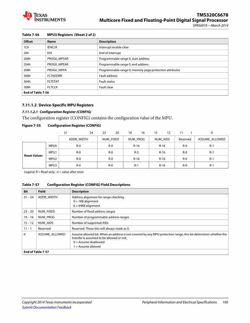
Multicore Fixed and Floating-Point Digital Signal Processor
Copyright 2014 Texas Instruments Incorporated Peripheral Information and Electrical Specifications 199
SPRS691E—March 2014
TMS320C6678
Submit Documentation Feedback
7.11.1.2 Device-Specific MPU Registers
7.11.1.2.1 Configuration Register (CONFIG)
The configuration register (CONFIG) contains the configuration value of the MPU.
1Ch IENCLR Interrupt enable clear
20h EOI End of interrupt
200h PROG0_MPSAR Programmable range 0, start address
204h PROG0_MPEAR Programmable range 0, end address
208h PROG0_MPPA Programmable range 0, memory page protection attributes
300h FLTADDRR Fault address
304h FLTSTAT Fault status
308h FLTCLR Fault clear
End of Table 7-56
Figure 7-35 Configuration Register (CONFIG)
31 24 23 20 19 16 15 12 11 1 0
ADDR_WIDTH NUM_FIXED NUM_PROG NUM_AIDS Reserved ASSUME_ALLOWED
Reset Values
MPU0 R-0 R-0 R-16 R-16 R-0 R-1
MPU1 R-0 R-0 R-5 R-16 R-0 R-1
MPU2 R-0 R-0 R-16 R-16 R-0 R-1
MPU3 R-0 R-0 R-1 R-16 R-0 R-1
Legend: R = Read only; -n = value after reset
Table 7-57 Configuration Register (CONFIG) Field Descriptions
Bit Field Description
31 – 24 ADDR_WIDTH Address alignment for range checking0 = 1KB alignment6 = 64KB alignment
23 – 20 NUM_FIXED Number of fixed address ranges
19 – 16 NUM_PROG Number of programmable address ranges
15 – 12 NUM_AIDS Number of supported AIDs
11 – 1 Reserved Reserved. These bits will always reads as 0.
0 ASSUME_ALLOWED Assume allowed bit. When an address is not covered by any MPU protection range, this bit determines whether the transfer is assumed to be allowed or not.
0 = Assume disallowed1 = Assume allowed
End of Table 7-57
Table 7-56 MPU3 Registers (Sheet 2 of 2)
Offset Name Description

200 Peripheral Information and Electrical Specifications Copyright 2014 Texas Instruments Incorporated
SPRS691E—March 2014Multicore Fixed and Floating-Point Digital Signal ProcessorTMS320C6678
Submit Documentation Feedback
7.11.2 MPU Programmable Range Registers
7.11.2.1 Programmable Range n Start Address Register (PROGn_MPSAR)
The programmable address start register holds the start address for the range. This register is writeable only by a supervisor entity. If NS = 0 (non-secure mode) in the associated MPPA register, then the register is also writeable only by a secure entity.
The start address must be aligned on a page boundary. The size of the page is 1K byte. The size of the page determines the width of the address field in MPSAR and MPEAR.
7.11.2.2 Programmable Range n End Address Register (PROGn_MPEAR)
The programmable address end register holds the end address for the range. This register is writeable only by a supervisor entity. If NS = 0 (non-secure mode) in the associated MPPA register, then the register is also writeable only by a secure entity.
The end address must be aligned on a page boundary. The size of the page depends on the MPU number. The page size for MPU1 is 1K byte and for MPU2 it is 64K bytes. The size of the page determines the width of the address field in MPSAR and MPEAR
Figure 7-36 Programmable Range n Start Address Register (PROGn_MPSAR)
31 10 9 0
START_ADDR Reserved
R/W R
Legend: R = Read only; R/W = Read/Write
Table 7-58 Programmable Range n Start Address Register (PROGn_MPSAR) Field Descriptions
Bit Field Description
31 – 10 START_ADDR Start address for range n.
9 – 0 Reserved Reserved and these bits always read as 0.
End of Table 7-58
Figure 7-37 Programmable Range n End Address Register (PROGn_MPEAR)
31 10 9 0
END_ADDR Reserved
R/W R
Legend: R = Read only; R/W = Read/Write
Table 7-59 Programmable Range n End Address Register (PROGn_MPEAR) Field Descriptions
Bit Field Description
31 – 10 END_ADDR End address for range n.
9 – 0 Reserved Reserved and these bits always read as 3FFh.
End of Table 7-59

Multicore Fixed and Floating-Point Digital Signal Processor
Copyright 2014 Texas Instruments Incorporated Peripheral Information and Electrical Specifications 201
SPRS691E—March 2014
TMS320C6678
Submit Documentation Feedback
7.11.2.3 Programmable Range n Memory Protection Page Attribute Register (PROGn_MPPA)
The programmable address memory protection page attribute register holds the permissions for the region. This register is writeable only by a non-debug supervisor entity. If NS = 0 (secure mode), then the register is also writeable only by a non-debug secure entity. The NS bit is writeable only by a non-debug secure entity. For debug accesses, the register is writeable only when NS = 1 or EMU = 1.Figure 7-38 Programmable Range n Memory Protection Page Attribute Register (PROGn_MPPA)
31 26 25 24 23 22 21 20 19 18 17 16 15
Reserved AID15 AID14 AID13 AID12 AID11 AID10 AID9 AID8 AID7 AID6 AID5
R R/W R/W R/W R/W R/W R/W R/W R/W R/W R/W R/W
14 13 12 11 10 9 8 7 6 5 4 3 2 1 0
AID4 AID3 AID2 AID1 AID0 AIDX Reserved NS EMU SR SW SX UR UW UX
R/W R/W R/W R/W R/W R/W R R/W R/W R/W R/W R/W R/W R/W R/W
Legend: R = Read only; R/W = Read/Write
Table 7-60 Programmable Range n Memory Protection Page Attribute Register (PROGn_MPPA) Field Descriptions (Sheet 1 of 2)
Bit Field Description
31 – 26 Reserved Reserved. These bits will always reads as 0.
25 AID15 Controls permission check of ID = 150 = AID is not checked for permissions1 = AID is checked for permissions
24 AID14 Controls permission check of ID = 140 = AID is not checked for permissions1 = AID is checked for permissions
23 AID13 Controls permission check of ID = 130 = AID is not checked for permissions1 = AID is checked for permissions
22 AID12 Controls permission check of ID = 120 = AID is not checked for permissions1 = AID is checked for permissions
21 AID11 Controls permission check of ID = 110 = AID is not checked for permissions1 = AID is checked for permissions
20 AID10 Controls permission check of ID = 100 = AID is not checked for permissions1 = AID is checked for permissions
19 AID9 Controls permission check of ID = 90 = AID is not checked for permissions1 = AID is checked for permissions
18 AID8 Controls permission check of ID = 80 = AID is not checked for permissions1 = AID is checked for permissions
17 AID7 Controls permission check of ID = 70 = AID is not checked for permissions1 = AID is checked for permissions
16 AID6 Controls permission check of ID = 60 = AID is not checked for permissions1 = AID is checked for permissions

202 Peripheral Information and Electrical Specifications Copyright 2014 Texas Instruments Incorporated
SPRS691E—March 2014Multicore Fixed and Floating-Point Digital Signal ProcessorTMS320C6678
Submit Documentation Feedback
15 AID5 Controls permission check of ID = 50 = AID is not checked for permissions1 = AID is checked for permissions
14 AID4 Controls permission check of ID = 40 = AID is not checked for permissions1 = AID is checked for permissions
13 AID3 Controls permission check of ID = 30 = AID is not checked for permissions1 = AID is checked for permissions
12 AID2 Controls permission check of ID = 20 = AID is not checked for permissions1 = AID is checked for permissions
11 AID1 Controls permission check of ID = 10 = AID is not checked for permissions1 = AID is checked for permissions
10 AID0 Controls permission check of ID = 00 = AID is not checked for permissions1 = AID is checked for permissions
9 AIDX Controls permission check of ID > 150 = AID is not checked for permissions1 = AID is checked for permissions
8 Reserved Always reads as 0.
7 NS Non-secure access permission0 = Only secure access allowed.1 = Non-secure access allowed.
6 EMU Emulation (debug) access permission. This bit is ignored if NS = 10 = Debug access not allowed.1 = Debug access allowed.
5 SR Supervisor Read permission0 = Access not allowed.1 = Access allowed.
4 SW Supervisor Write permission0 = Access not allowed.1 = Access allowed.
3 SX Supervisor Execute permission0 = Access not allowed.1 = Access allowed.
2 UR User Read permission0 = Access not allowed.1 = Access allowed
1 UW User Write permission0 = Access not allowed.1 = Access allowed.
0 UX User Execute permission
0 = Access not allowed.
1 = Access allowed.
End of Table 7-601
Table 7-60 Programmable Range n Memory Protection Page Attribute Register (PROGn_MPPA) Field Descriptions (Sheet 2 of 2)
Bit Field Description
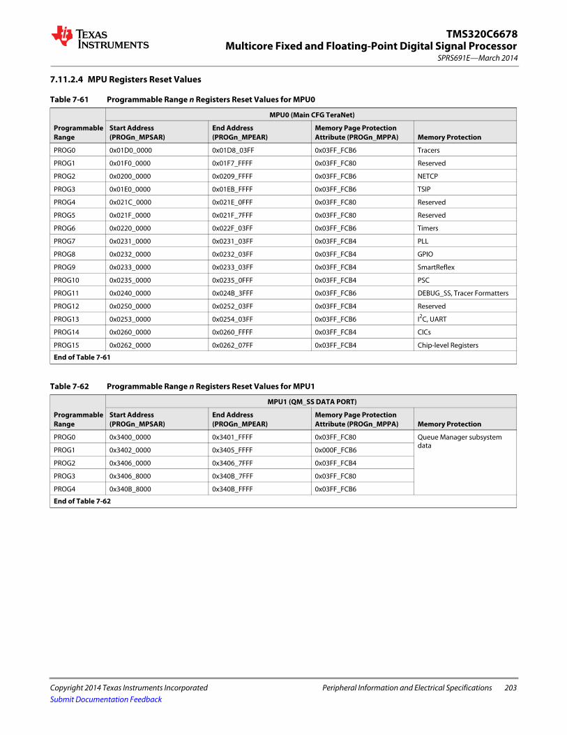
Multicore Fixed and Floating-Point Digital Signal Processor
Copyright 2014 Texas Instruments Incorporated Peripheral Information and Electrical Specifications 203
SPRS691E—March 2014
TMS320C6678
Submit Documentation Feedback
7.11.2.4 MPU Registers Reset Values
Table 7-61 Programmable Range n Registers Reset Values for MPU0
Programmable Range
MPU0 (Main CFG TeraNet)
Start Address (PROGn_MPSAR)
End Address (PROGn_MPEAR)
Memory Page Protection Attribute (PROGn_MPPA) Memory Protection
PROG0 0x01D0_0000 0x01D8_03FF 0x03FF_FCB6 Tracers
PROG1 0x01F0_0000 0x01F7_FFFF 0x03FF_FC80 Reserved
PROG2 0x0200_0000 0x0209_FFFF 0x03FF_FCB6 NETCP
PROG3 0x01E0_0000 0x01EB_FFFF 0x03FF_FCB6 TSIP
PROG4 0x021C_0000 0x021E_0FFF 0x03FF_FC80 Reserved
PROG5 0x021F_0000 0x021F_7FFF 0x03FF_FC80 Reserved
PROG6 0x0220_0000 0x022F_03FF 0x03FF_FCB6 Timers
PROG7 0x0231_0000 0x0231_03FF 0x03FF_FCB4 PLL
PROG8 0x0232_0000 0x0232_03FF 0x03FF_FCB4 GPIO
PROG9 0x0233_0000 0x0233_03FF 0x03FF_FCB4 SmartReflex
PROG10 0x0235_0000 0x0235_0FFF 0x03FF_FCB4 PSC
PROG11 0x0240_0000 0x024B_3FFF 0x03FF_FCB6 DEBUG_SS, Tracer Formatters
PROG12 0x0250_0000 0x0252_03FF 0x03FF_FCB4 Reserved
PROG13 0x0253_0000 0x0254_03FF 0x03FF_FCB6 I2C, UART
PROG14 0x0260_0000 0x0260_FFFF 0x03FF_FCB4 CICs
PROG15 0x0262_0000 0x0262_07FF 0x03FF_FCB4 Chip-level Registers
End of Table 7-61
Table 7-62 Programmable Range n Registers Reset Values for MPU1
Programmable Range
MPU1 (QM_SS DATA PORT)
Start Address (PROGn_MPSAR)
End Address (PROGn_MPEAR)
Memory Page Protection Attribute (PROGn_MPPA) Memory Protection
PROG0 0x3400_0000 0x3401_FFFF 0x03FF_FC80 Queue Manager subsystem data
PROG1 0x3402_0000 0x3405_FFFF 0x000F_FCB6
PROG2 0x3406_0000 0x3406_7FFF 0x03FF_FCB4
PROG3 0x3406_8000 0x340B_7FFF 0x03FF_FC80
PROG4 0x340B_8000 0x340B_FFFF 0x03FF_FCB6
End of Table 7-62

204 Peripheral Information and Electrical Specifications Copyright 2014 Texas Instruments Incorporated
SPRS691E—March 2014Multicore Fixed and Floating-Point Digital Signal ProcessorTMS320C6678
Submit Documentation Feedback
Table 7-63 Programmable Range n Registers Reset Values for MPU2
Programmable Range
MPU2 (QM_SS CFG PORT)
Start Address (PROGn_MPSAR)
End Address (PROGn_MPEAR)
Memory Page Protection Attribute (PROGn_MPPA) Memory Protection
PROG0 0x02A0_0000 0x02A1_FFFF 0x03FF_FCA4 Queue Manager subsystem configuration
PROG1 0x02A2_0000 0x02A3_FFFF 0x000F_FCB6
PROG2 0x02A4_0000 0x02A5_FFFF 0x000F_FCB6
PROG3 0x02A6_0000 0x02A6_7FFF 0x03FF_FCB4
PROG4 0x02A6_8000 0x02A6_8FFF 0x03FF_FCB4
PROG5 0x02A6_9000 0x02A6_9FFF 0x03FF_FCB4
PROG6 0x02A6_A000 0x02A6_AFFF 0x03FF_FCB4
PROG7 0x02A6_B000 0x02A6_BFFF 0x03FF_FCB4
PROG8 0x02A6_C000 0x02A6_DFFF 0x03FF_FCB4
PROG9 0x02A6_E000 0x02A6_FFFF 0x03FF_FCB4
PROG10 0x02A8_0000 0x02A8_FFFF 0x03FF_FCA4
PROG11 0x02A9_0000 0x02A9_FFFF 0x03FF_FCB4
PROG12 0x02AA_0000 0x02AA_7FFF 0x03FF_FCB4
PROG13 0x02AA_8000 0x02AA_FFFF 0x03FF_FCB4
PROG14 0x02AB_0000 0x02AB_7FFF 0x03FF_FCB4
PROG15 0x02AB_8000 0x02AB_FFFF 0x03FF_FCB6
End of Table 7-63
Table 7-64 Programmable Range n Registers Reset Values for MPU3
Programmable Range
MPU3 (Semaphore)
Start Address (PROGn_MPSAR)
End Address (PROGn_MPEAR)
Memory Page Protection Attributes (PROGn_MPPA) Memory Protection
PROG0 0x0264_0000 0x0264_07FF 0x0003_FCB6 Semaphore
End of Table 7-64

Multicore Fixed and Floating-Point Digital Signal Processor
Copyright 2014 Texas Instruments Incorporated Peripheral Information and Electrical Specifications 205
SPRS691E—March 2014
TMS320C6678
Submit Documentation Feedback
7.12 DDR3 Memory ControllerThe 64-bit DDR3 Memory Controller bus of the TMS320C6678 is used to interface to JEDEC standard-compliant DDR3 SDRAM devices. The DDR3 external bus interfaces only to DDR3 SDRAM devices; it does not share the bus with any other types of peripherals.
7.12.1 DDR3 Memory Controller Device-Specific Information
The TMS320C6678 includes one 64-bit wide 1.5-V DDR3 SDRAM EMIF interface. The DDR3 interface can operate at 800 Mega Transfers per Second (MTS), 1066 MTS, 1333 MTS, and 1600 MTS.
Due to the complicated nature of the interface, a limited number of topologies are supported to provide a 16-bit, 32-bit, or 64-bit interface.
The DDR3 electrical requirements are fully specified in the DDR Jedec Specification JESD79-3C. Standard DDR3 SDRAMs are available in 8- and 16-bit versions, allowing for the following bank topologies to be supported by the interface:
• 72-bit: Five 16-bit SDRAMs (including 8 bits of ECC)• 72-bit: Nine 8-bit SDRAMs (including 8 bits of ECC)• 36-bit: Three 16-bit SDRAMs (including 4 bits of ECC)• 36-bit: Five 8-bit SDRAMs (including 4 bits of ECC)• 64-bit: Four 16-bit SDRAMs• 64-bit: Eight 8-bit SDRAMs• 32-bit: Two 16-bit SDRAMs• 32-bit: Four 8-bit SDRAMs• 16-bit: One 16-bit SDRAM• 16-bit: Two 8-bit SDRAM
The approach to specifying interface timing for the DDR3 memory bus is different than on other interfaces such as I2C or SPI. For these other interfaces, the device timing was specified in terms of data manual specifications and I/O buffer information specification (IBIS) models. For the DDR3 memory bus, the approach is to specify compatible DDR3 devices and provide the printed circuit board (PCB) solution and guidelines directly to the user.
7.12.2 DDR3 Memory Controller Race Condition Consideration
A race condition may exist when certain masters write data to the DDR3 memory controller. For example, if master A passes a software message via a buffer in external memory and does not wait for an indication that the write completes, before signaling to master B that the message is ready, when master B attempts to read the software message, then the master B read may bypass the master A write and, thus, master B may read stale data and, therefore, receive an incorrect message.
Some master peripherals (e.g., EDMA3 transfer controllers with TCCMOD=0) will always wait for the write to complete before signaling an interrupt to the system, thus avoiding this race condition. For masters that do not have a hardware specification of write-read ordering, it may be necessary to specify data ordering via software.
If master A does not wait for indication that a write is complete, it must perform the following workaround: 1. Perform the required write to DDR3 memory space. 2. Perform a dummy write to the DDR3 memory controller module ID and revision register. 3. Perform a dummy read to the DDR3 memory controller module ID and revision register. 4. Indicate to master B that the data is ready to be read after completion of the read in step 3. The completion of
the read in step 3 ensures that the previous write was done.
206 Peripheral Information and Electrical Specifications Copyright 2014 Texas Instruments Incorporated
SPRS691E—March 2014Multicore Fixed and Floating-Point Digital Signal ProcessorTMS320C6678
Submit Documentation Feedback
7.12.3 DDR3 Memory Controller Electrical Data/Timing
The DDR3 Design Requirements for KeyStone Devices in ‘‘Related Documentation from Texas Instruments’’ on page 72 specifies a complete DDR3 interface solution as well as a list of compatible DDR3 devices. The DDR3 electrical requirements are fully specified in the DDR3 Jedec Specification JESD79-3C. TI has performed the simulation and system characterization to ensure all DDR3 interface timings in this solution are met; therefore, no electrical data/timing information is supplied here for this interface.
Note—TI supports only designs that follow the board design guidelines outlined in the application report.

Multicore Fixed and Floating-Point Digital Signal Processor
Copyright 2014 Texas Instruments Incorporated Peripheral Information and Electrical Specifications 207
SPRS691E—March 2014
TMS320C6678
Submit Documentation Feedback
7.13 I2C PeripheralThe inter-integrated circuit (I2C) module provides an interface between DSP and other devices compliant with Philips Semiconductors Inter-IC bus (I2C bus) specification version 2.1 and connected by way of an I2C bus. External components attached to this 2-wire serial bus can transmit/receive up to 8-bit data to/from the DSP through the I2C module.
7.13.1 I2C Device-Specific Information
The TMS320C6678 device includes an I2C peripheral module.
Note—When using the I2C module, ensure there are external pullup resistors on the SDA and SCL pins.
The I2C modules on the C6678 may be used by the DSP to control local peripheral ICs (DACs, ADCs, etc.) or may be used to communicate with other controllers in a system or to implement a user interface.
The I2C port is compatible with Philips I2C specification revision 2.1 (January 2000) and supports:• Fast mode up to 400 Kbps (no fail-safe I/O buffers)• Noise filter to remove noise 50 ns or less• 7-bit and 10-bit device addressing modes• Multi-master (transmit/receive) and slave (transmit/receive) functionality• Events: DMA, interrupt, or polling• Slew-rate limited open-drain output buffers

208 Peripheral Information and Electrical Specifications Copyright 2014 Texas Instruments Incorporated
SPRS691E—March 2014Multicore Fixed and Floating-Point Digital Signal ProcessorTMS320C6678
Submit Documentation Feedback
Figure 7-39 shows a block diagram of the I2C module.Figure 7-39 I2C Module Block Diagram
7.13.2 I2C Peripheral Register Description(s)
Table 7-65 I2C Registers (Sheet 1 of 2)
Hex Address Range Register Register Name
0253 0000 ICOAR I2C Own Address Register
0253 0004 ICIMR I2C Interrupt Mask/Status Register
0253 0008 ICSTR I2C Interrupt Status Register
0253 000C ICCLKL I2C Clock Low-Time Divider Register
0253 0010 ICCLKH I2C Clock High-Time Divider Register
0253 0014 ICCNT I2C Data Count Register
0253 0018 ICDRR I2C Data Receive Register
0253 001C ICSAR I2C Slave Address Register
0253 0020 ICDXR I2C Data Transmit Register
0253 0024 ICMDR I2C Mode Register
0253 0028 ICIVR I2C Interrupt Vector Register
0253 002C ICEMDR I2C Extended Mode Register
ClockPrescale
I CPSC2
Peripheral Clock(CPU/6)
I CCLKH2
GeneratorBit Clock
I CCLKL2
NoiseFilter
SCL
I CXSR2
I CDXR2
Transmit
TransmitShift
TransmitBuffer
I CDRR2
ShiftI CRSR2
ReceiveBuffer
Receive
Receive
Filter
SDA
I C Data2 Noise
I COAR2
I CSAR2 SlaveAddress
Control
AddressOwn
I CMDR2
I CCNT2
Mode
DataCount
VectorInterrupt
InterruptStatus
I CIVR2
I CSTR2
Mask/StatusInterrupt
I CIMR2
Interrupt/DMA
I C Module2
I C Clock2
Shading denotes control/status registers.
I CEMDR2 ExtendedMode
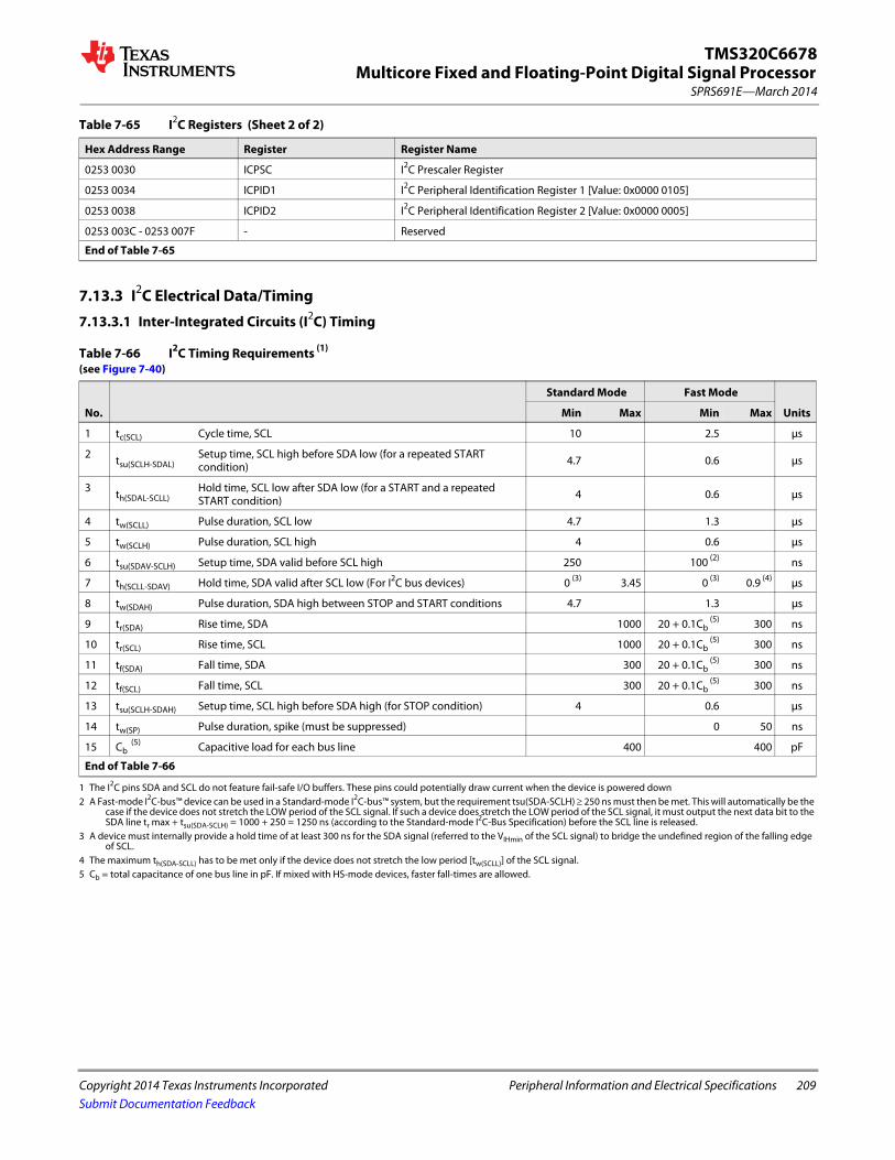
Multicore Fixed and Floating-Point Digital Signal Processor
Copyright 2014 Texas Instruments Incorporated Peripheral Information and Electrical Specifications 209
SPRS691E—March 2014
TMS320C6678
Submit Documentation Feedback
7.13.3 I2C Electrical Data/Timing
7.13.3.1 Inter-Integrated Circuits (I2C) Timing
0253 0030 ICPSC I2C Prescaler Register
0253 0034 ICPID1 I2C Peripheral Identification Register 1 [Value: 0x0000 0105]
0253 0038 ICPID2 I2C Peripheral Identification Register 2 [Value: 0x0000 0005]
0253 003C - 0253 007F - Reserved
End of Table 7-65
Table 7-66 I2C Timing Requirements (1) (see Figure 7-40)
1 The I2C pins SDA and SCL do not feature fail-safe I/O buffers. These pins could potentially draw current when the device is powered down
No.
Standard Mode Fast Mode
UnitsMin Max Min Max
1 tc(SCL) Cycle time, SCL 10 2.5 μs
2 tsu(SCLH-SDAL) Setup time, SCL high before SDA low (for a repeated START condition) 4.7 0.6 μs
3 th(SDAL-SCLL) Hold time, SCL low after SDA low (for a START and a repeated START condition) 4 0.6 μs
4 tw(SCLL) Pulse duration, SCL low 4.7 1.3 μs
5 tw(SCLH) Pulse duration, SCL high 4 0.6 μs
6 tsu(SDAV-SCLH) Setup time, SDA valid before SCL high 250 100 (2)
2 A Fast-mode I2C-bus™ device can be used in a Standard-mode I2C-bus™ system, but the requirement tsu(SDA-SCLH) 250 ns must then be met. This will automatically be the case if the device does not stretch the LOW period of the SCL signal. If such a device does stretch the LOW period of the SCL signal, it must output the next data bit to the SDA line tr max + tsu(SDA-SCLH) = 1000 + 250 = 1250 ns (according to the Standard-mode I2C-Bus Specification) before the SCL line is released.
ns
7 th(SCLL-SDAV) Hold time, SDA valid after SCL low (For I2C bus devices) 0 (3)
3 A device must internally provide a hold time of at least 300 ns for the SDA signal (referred to the VIHmin of the SCL signal) to bridge the undefined region of the falling edge of SCL.
3.45 0 (3) 0.9 (4)
4 The maximum th(SDA-SCLL) has to be met only if the device does not stretch the low period [tw(SCLL)] of the SCL signal.
μs
8 tw(SDAH) Pulse duration, SDA high between STOP and START conditions 4.7 1.3 μs
9 tr(SDA) Rise time, SDA 1000 20 + 0.1Cb (5)
5 Cb = total capacitance of one bus line in pF. If mixed with HS-mode devices, faster fall-times are allowed.
300 ns
10 tr(SCL) Rise time, SCL 1000 20 + 0.1Cb(5) 300 ns
11 tf(SDA) Fall time, SDA 300 20 + 0.1Cb(5) 300 ns
12 tf(SCL) Fall time, SCL 300 20 + 0.1Cb(5) 300 ns
13 tsu(SCLH-SDAH) Setup time, SCL high before SDA high (for STOP condition) 4 0.6 μs
14 tw(SP) Pulse duration, spike (must be suppressed) 0 50 ns
15 Cb (5) Capacitive load for each bus line 400 400 pF
End of Table 7-66
Table 7-65 I2C Registers (Sheet 2 of 2)
Hex Address Range Register Register Name

210 Peripheral Information and Electrical Specifications Copyright 2014 Texas Instruments Incorporated
SPRS691E—March 2014Multicore Fixed and Floating-Point Digital Signal ProcessorTMS320C6678
Submit Documentation Feedback
Figure 7-40 I2C Receive Timings
Table 7-67 I2C Switching Characteristics (1) (see Figure 7-41)
1 Cb = total capacitance of one bus line in pF. If mixed with HS-mode devices, faster fall-times are allowed.
No. Parameter
Standard Mode Fast Mode
UnitMin Max Min Max
16 tc(SCL) Cycle time, SCL 10 2.5 ms
17 tsu(SCLH-SDAL) Setup time, SCL high to SDA low (for a repeated START condition) 4.7 0.6 ms
18 th(SDAL-SCLL) Hold time, SDA low after SCL low (for a START and a repeated START condition) 4 0.6 ms
19 tw(SCLL) Pulse duration, SCL low 4.7 1.3 ms
20 tw(SCLH) Pulse duration, SCL high 4 0.6 ms
21 td(SDAV-SDLH) Delay time, SDA valid to SCL high 250 100 ns
22 tv(SDLL-SDAV) Valid time, SDA valid after SCL low (For I2C bus devices) 0 0 0.9 ms
23 tw(SDAH) Pulse duration, SDA high between STOP and START conditions 4.7 1.3 ms
24 tr(SDA) Rise time, SDA 1000 20 + 0.1Cb(1) 300 ns
25 tr(SCL) Rise time, SCL 1000 20 + 0.1Cb(1) 300 ns
26 tf(SDA) Fall time, SDA 300 20 + 0.1Cb(1) 300 ns
27 tf(SCL) Fall time, SCL 300 20 + 0.1Cb(1) 300 ns
28 td(SCLH-SDAH) Delay time, SCL high to SDA high (for STOP condition) 4 0.6 ms
29 Cp Capacitance for each I2C pin 10 10 pF
End of Table 7-67
10
8
4
37
12
5
6 14
2
3
13
Stop Start RepeatedStart
Stop
SDA
SCL
1
11 9
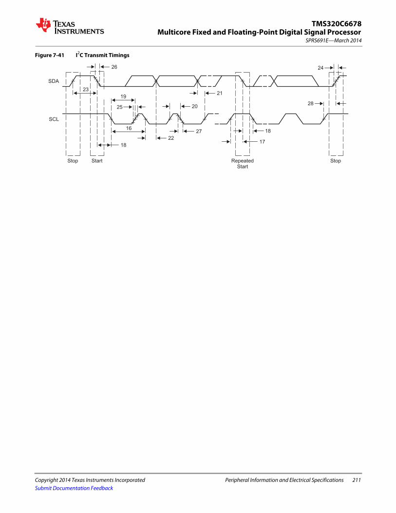
Multicore Fixed and Floating-Point Digital Signal Processor
Copyright 2014 Texas Instruments Incorporated Peripheral Information and Electrical Specifications 211
SPRS691E—March 2014
TMS320C6678
Submit Documentation Feedback
Figure 7-41 I2C Transmit Timings
25
23
19
18
22
27
20
21
17
18
28
Stop Start RepeatedStart
Stop
SDA
SCL
16
26 24

212 Peripheral Information and Electrical Specifications Copyright 2014 Texas Instruments Incorporated
SPRS691E—March 2014Multicore Fixed and Floating-Point Digital Signal ProcessorTMS320C6678
Submit Documentation Feedback
7.14 SPI PeripheralThe serial peripheral interconnect (SPI) module provides an interface between the DSP and other SPI-compliant devices. The primary intent of this interface is to allow for connection to a SPI ROM for boot. The SPI module on C6678 is supported only in master mode. Additional chip-level components can also be included, such as temperature sensors or an I/O expander.
The C6678 SPI supports two modes, 3-pin and 4-pin. For the 4-pin chip-select mode, the C6678 supports up to two chip selects.
7.14.1 SPI Electrical Data/Timing
7.14.1.1 SPI Timing
Table 7-68 SPI Timing Requirements See Figure 7-42)
No. Min Max Unit
Master Mode Timing Diagrams — Base Timings for 3 Pin Mode
7 tsu(SDI-SPC) Input Setup Time, SPIDIN valid before receive edge of SPICLK. Polarity = 0 Phase = 0 2 ns
7 tsu(SDI-SPC) Input Setup Time, SPIDIN valid before receive edge of SPICLK. Polarity = 0 Phase = 1 2 ns
7 tsu(SDI-SPC) Input Setup Time, SPIDIN valid before receive edge of SPICLK. Polarity = 1 Phase = 0 2 ns
7 tsu(SDI-SPC) Input Setup Time, SPIDIN valid before receive edge of SPICLK. Polarity = 1 Phase = 1 2 ns
8 th(SPC-SDI) Input Hold Time, SPIDIN valid after receive edge of SPICLK. Polarity = 0 Phase = 0 5 ns
8 th(SPC-SDI) Input Hold Time, SPIDIN valid after receive edge of SPICLK. Polarity = 0 Phase = 1 5 ns
8 th(SPC-SDI) Input Hold Time, SPIDIN valid after receive edge of SPICLK. Polarity = 1 Phase = 0 5 ns
8 th(SPC-SDI) Input Hold Time, SPIDIN valid after receive edge of SPICLK. Polarity = 1 Phase = 1 5 ns
End of Table 7-68
Table 7-69 SPI Switching Characteristics (Sheet 1 of 2)(See Figure 7-42 and Figure 7-43)
No. Parameter Min Max Unit
Master Mode Timing Diagrams — Base Timings for 3 Pin Mode
1 tc(SPC) Cycle Time, SPICLK, All Master Modes 3*P2 (1) ns
2 tw(SPCH) Pulse Width High, SPICLK, All Master Modes 0.5*tc - 1 ns
3 tw(SPCL) Pulse Width Low, SPICLK, All Master Modes 0.5*tc - 1 ns
4 td(SDO-SPC) Setup (Delay), initial data bit valid on SPIDOUT to initial edge on SPICLK. Polarity = 0, Phase = 0.
5 ns
4 td(SDO-SPC) Setup (Delay), initial data bit valid on SPIDOUT to initial edge on SPICLK. Polarity = 0, Phase = 1.
5 ns
4 td(SDO-SPC) Setup (Delay), initial data bit valid on SPIDOUT to initial edge on SPICLK Polarity = 1, Phase = 0
5 ns
4 td(SDO-SPC) Setup (Delay), initial data bit valid on SPIDOUT to initial edge on SPICLK Polarity = 1, Phase = 1
5 ns
5 td(SPC-SDO) Setup (Delay), subsequent data bits valid on SPIDOUT to initial edge on SPICLK. Polarity = 0 Phase = 0
2 ns
5 td(SPC-SDO) Setup (Delay), subsequent data bits valid on SPIDOUT to initial edge on SPICLK Polarity = 0 Phase = 1
2 ns
5 td(SPC-SDO) Setup (Delay), subsequent data bits valid on SPIDOUT to initial edge on SPICLK Polarity = 1 Phase = 0
2 ns
5 td(SPC-SDO) Setup (Delay), subsequent data bits valid on SPIDOUT to initial edge on SPICLK Polarity = 1 Phase = 1
2 ns
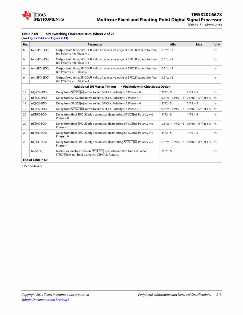
Multicore Fixed and Floating-Point Digital Signal Processor
Copyright 2014 Texas Instruments Incorporated Peripheral Information and Electrical Specifications 213
SPRS691E—March 2014
TMS320C6678
Submit Documentation Feedback
6 toh(SPC-SDO) Output hold time, SPIDOUT valid after receive edge of SPICLK except for final bit. Polarity = 0 Phase = 0
0.5*tc - 2 ns
6 toh(SPC-SDO) Output hold time, SPIDOUT valid after receive edge of SPICLK except for final bit. Polarity = 0 Phase = 1
0.5*tc - 2 ns
6 toh(SPC-SDO) Output hold time, SPIDOUT valid after receive edge of SPICLK except for final bit. Polarity = 1 Phase = 0
0.5*tc - 2 ns
6 toh(SPC-SDO) Output hold time, SPIDOUT valid after receive edge of SPICLK except for final bit. Polarity = 1 Phase = 1
0.5*tc - 2 ns
Additional SPI Master Timings — 4 Pin Mode with Chip Select Option
19 td(SCS-SPC) Delay from SPISCS[n] active to first SPICLK. Polarity = 0 Phase = 0 2*P2 - 5 2*P2 + 5 ns
19 td(SCS-SPC) Delay from SPISCS[n] active to first SPICLK. Polarity = 0 Phase = 1 0.5*tc + (2*P2) - 5 0.5*tc + (2*P2) + 5 ns
19 td(SCS-SPC) Delay from SPISCS[n] active to first SPICLK. Polarity = 1 Phase = 0 2*P2 - 5 2*P2 + 5 ns
19 td(SCS-SPC) Delay from SPISCS[n] active to first SPICLK. Polarity = 1 Phase = 1 0.5*tc + (2*P2) - 5 0.5*tc + (2*P2) + 5 ns
20 td(SPC-SCS) Delay from final SPICLK edge to master deasserting SPISCS[n]. Polarity = 0 Phase = 0
1*P2 - 5 1*P2 + 5 ns
20 td(SPC-SCS) Delay from final SPICLK edge to master deasserting SPISCS[n]. Polarity = 0 Phase = 1
0.5*tc + (1*P2) - 5 0.5*tc + (1*P2) + 5 ns
20 td(SPC-SCS) Delay from final SPICLK edge to master deasserting SPISCS[n]. Polarity = 1 Phase = 0
1*P2 - 5 1*P2 + 5 ns
20 td(SPC-SCS) Delay from final SPICLK edge to master deasserting SPISCS[n]. Polarity = 1 Phase = 1
0.5*tc + (1*P2) - 5 0.5*tc + (1*P2) + 5 ns
tw(SCSH) Minimum inactive time on SPISCS[n] pin between two transfers when SPISCS[n] is not held using the CSHOLD feature.
2*P2 - 5 ns
End of Table 7-69
1 P2 = 1/SYSCLK7
Table 7-69 SPI Switching Characteristics (Sheet 2 of 2)(See Figure 7-42 and Figure 7-43)
No. Parameter Min Max Unit

214 Peripheral Information and Electrical Specifications Copyright 2014 Texas Instruments Incorporated
SPRS691E—March 2014Multicore Fixed and Floating-Point Digital Signal ProcessorTMS320C6678
Submit Documentation Feedback
Figure 7-42 SPI Master Mode Timing Diagrams — Base Timings for 3 Pin Mode
Figure 7-43 SPI Additional Timings for 4 Pin Master Mode with Chip Select Option
SPICLK
SPIDOUT
SPIDIN
SPICLK
SPIDOUT
SPIDIN
SPICLK
SPIDOUT
SPIDIN
SPICLK
SPIDOUT
SPIDIN
MO(0) MO(1) MO(n−1) MO(n)
MI(0) MI(1) MI(n−1) MI(n)
MO(0) MO(1) MO(n−1) MO(n)
MI(0) MI(1) MI(n−1) MI(n)
MO(0) MO(1) MO(n−1) MO(n)
MI(0) MI(1) MI(n−1) MI(n)
MO(0) MO(1) MO(n−1) MO(n)
MI(0) MI(1) MI(n−1) MI(n)
6
6
7
7
7
7
8
8
8
8
32
6
1
4
4
4
4 5
5
5 6
MASTER MODE
POLARITY = 0 PHASE = 0
MASTER MODE
POLARITY = 0 PHASE = 1
MASTER MODE
POLARITY = 1 PHASE = 0
MASTER MODE
POLARITY = 1 PHASE = 1
5
MASTER MODE 4 PIN WITH CHIP SELECT
SPICLK
SPIDOUT
SPIDIN
SPISCSx
MO(0) MO(1) MO(n−1) MO(n)
MI(0) MI(1) MI(n−1) MI(n)
19 20

Multicore Fixed and Floating-Point Digital Signal Processor
Copyright 2014 Texas Instruments Incorporated Peripheral Information and Electrical Specifications 215
SPRS691E—March 2014
TMS320C6678
Submit Documentation Feedback
7.15 HyperLink PeripheralThe TMS320C6678 includes the HyperLink bus for companion chip/die interfaces. This is a four-lane SerDes interface designed to operate at up to 12.5 Gbaud per lane. The supported data rates include 1.25 Gbaud, 3.125 Gbaud, 6.25 Gbaud, 10 Gbaud and 12.5 Gbaud. The interface is used to connect with external accelerators. The HyperLink links must be connected with DC coupling.
The interface includes the Serial Station Management Interfaces used to send power management and flow messages between devices. This consists of four LVCMOS inputs and four LVCMOS outputs configured as two 2-wire output buses and two 2-wire input buses. Each 2-wire bus includes a data signal and a clock signal.
7.15.1 HyperLink Device-Specific Interrupt Event
The HyperLink has 64 input events. Events 0 to 31come from the chip level interrupt controller and events 32 to 63 are from queue-pending signals from the Queue Manager to monitor some of the transmission queue status.
Table 7-70 HyperLink Events for C6678 (Sheet 1 of 2)
Event Number Event Event Description
0 CIC3_OUT8 Interrupt Controller output
1 CIC3_OUT9 Interrupt Controller output
2 CIC3_OUT10 Interrupt Controller output
3 CIC3_OUT11 Interrupt Controller output
4 CIC3_OUT12 Interrupt Controller output
5 CIC3_OUT13 Interrupt Controller output
6 CIC3_OUT14 Interrupt Controller output
7 CIC3_OUT15 Interrupt Controller output
8 CIC3_OUT16 Interrupt Controller output
9 CIC3_OUT17 Interrupt Controller output
10 CIC3_OUT18 Interrupt Controller output
11 CIC3_OUT19 Interrupt Controller output
12 CIC3_OUT20 Interrupt Controller output
13 CIC3_OUT21 Interrupt Controller output
14 CIC3_OUT22 Interrupt Controller output
15 CIC3_OUT23 Interrupt Controller output
16 CIC3_OUT24 Interrupt Controller output
17 CIC3_OUT25 Interrupt Controller output
18 CIC3_OUT26 Interrupt Controller output
19 CIC3_OUT27 Interrupt Controller output
20 CIC3_OUT28 Interrupt Controller output
21 CIC3_OUT29 Interrupt Controller output
22 CIC3_OUT30 Interrupt Controller output
23 CIC3_OUT31 Interrupt Controller output
24 CIC3_OUT32 Interrupt Controller output
25 CIC3_OUT33 Interrupt Controller output
26 CIC3_OUT34 Interrupt Controller output
27 CIC3_OUT35 Interrupt Controller output
28 CIC3_OUT36 Interrupt Controller output
29 CIC3_OUT37 Interrupt Controller output

216 Peripheral Information and Electrical Specifications Copyright 2014 Texas Instruments Incorporated
SPRS691E—March 2014Multicore Fixed and Floating-Point Digital Signal ProcessorTMS320C6678
Submit Documentation Feedback
30 CIC3_OUT38 Interrupt Controller output
31 CIC3_OUT39 Interrupt Controller output
32 QM_INT_PEND_864 Queue manager pend event
33 QM_INT_PEND_865 Queue manager pend event
34 QM_INT_PEND_866 Queue manager pend event
35 QM_INT_PEND_867 Queue manager pend event
36 QM_INT_PEND_868 Queue manager pend event
37 QM_INT_PEND_869 Queue manager pend event
38 QM_INT_PEND_870 Queue manager pend event
39 QM_INT_PEND_871 Queue manager pend event
40 QM_INT_PEND_872 Queue manager pend event
41 QM_INT_PEND_873 Queue manager pend event
42 QM_INT_PEND_874 Queue manager pend event
43 QM_INT_PEND_875 Queue manager pend event
44 QM_INT_PEND_876 Queue manager pend event
45 QM_INT_PEND_877 Queue manager pend event
46 QM_INT_PEND_878 Queue manager pend event
47 QM_INT_PEND_879 Queue manager pend event
48 QM_INT_PEND_880 Queue manager pend event
49 QM_INT_PEND_881 Queue manager pend event
50 QM_INT_PEND_882 Queue manager pend event
51 QM_INT_PEND_883 Queue manager pend event
52 QM_INT_PEND_884 Queue manager pend event
53 QM_INT_PEND_885 Queue manager pend event
54 QM_INT_PEND_886 Queue manager pend event
55 QM_INT_PEND_887 Queue manager pend event
56 QM_INT_PEND_888 Queue manager pend event
57 QM_INT_PEND_889 Queue manager pend event
58 QM_INT_PEND_890 Queue manager pend event
59 QM_INT_PEND_891 Queue manager pend event
60 QM_INT_PEND_892 Queue manager pend event
61 QM_INT_PEND_893 Queue manager pend event
62 QM_INT_PEND_894 Queue manager pend event
63 QM_INT_PEND_895 Queue manager pend event
End of Table 7-70
Table 7-70 HyperLink Events for C6678 (Sheet 2 of 2)
Event Number Event Event Description
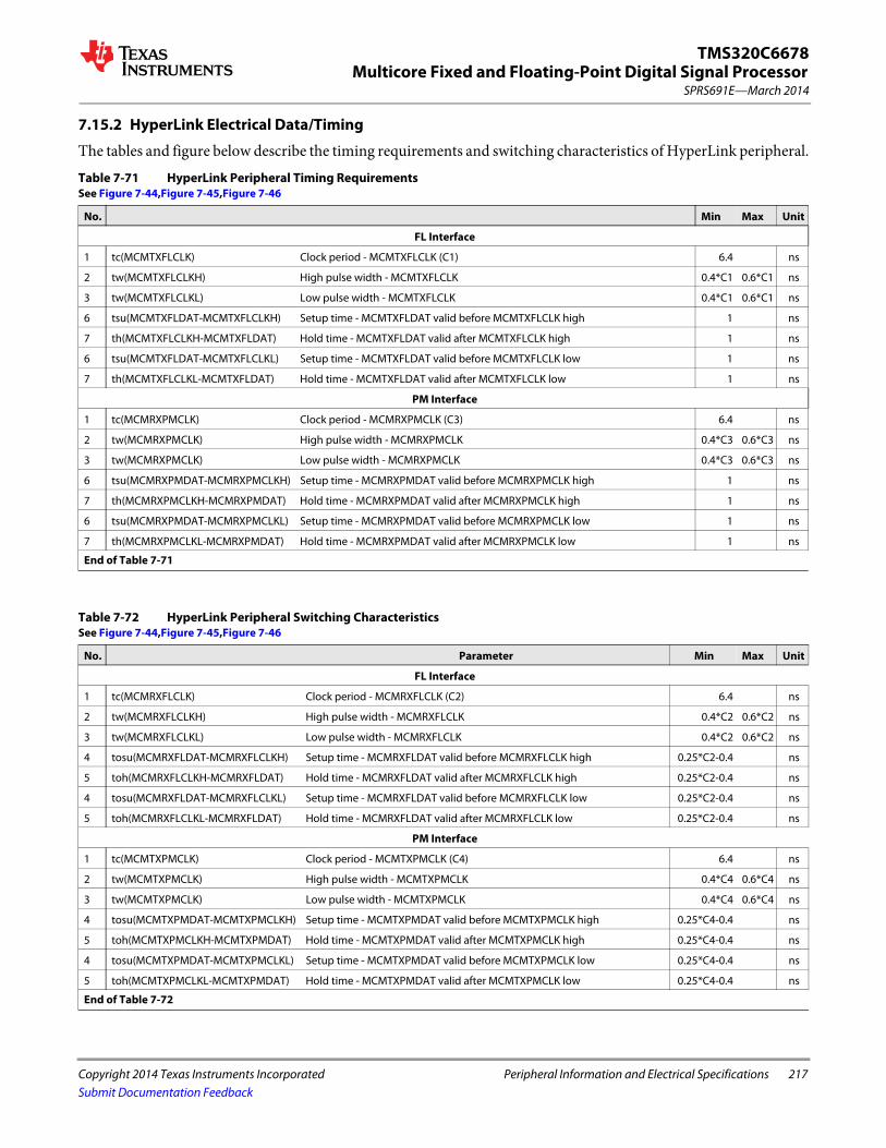
Multicore Fixed and Floating-Point Digital Signal Processor
Copyright 2014 Texas Instruments Incorporated Peripheral Information and Electrical Specifications 217
SPRS691E—March 2014
TMS320C6678
Submit Documentation Feedback
7.15.2 HyperLink Electrical Data/Timing
The tables and figure below describe the timing requirements and switching characteristics of HyperLink peripheral.Table 7-71 HyperLink Peripheral Timing Requirements See Figure 7-44,Figure 7-45,Figure 7-46
No. Min Max Unit
FL Interface
1 tc(MCMTXFLCLK) Clock period - MCMTXFLCLK (C1) 6.4 ns
2 tw(MCMTXFLCLKH) High pulse width - MCMTXFLCLK 0.4*C1 0.6*C1 ns
3 tw(MCMTXFLCLKL) Low pulse width - MCMTXFLCLK 0.4*C1 0.6*C1 ns
6 tsu(MCMTXFLDAT-MCMTXFLCLKH) Setup time - MCMTXFLDAT valid before MCMTXFLCLK high 1 ns
7 th(MCMTXFLCLKH-MCMTXFLDAT) Hold time - MCMTXFLDAT valid after MCMTXFLCLK high 1 ns
6 tsu(MCMTXFLDAT-MCMTXFLCLKL) Setup time - MCMTXFLDAT valid before MCMTXFLCLK low 1 ns
7 th(MCMTXFLCLKL-MCMTXFLDAT) Hold time - MCMTXFLDAT valid after MCMTXFLCLK low 1 ns
PM Interface
1 tc(MCMRXPMCLK) Clock period - MCMRXPMCLK (C3) 6.4 ns
2 tw(MCMRXPMCLK) High pulse width - MCMRXPMCLK 0.4*C3 0.6*C3 ns
3 tw(MCMRXPMCLK) Low pulse width - MCMRXPMCLK 0.4*C3 0.6*C3 ns
6 tsu(MCMRXPMDAT-MCMRXPMCLKH) Setup time - MCMRXPMDAT valid before MCMRXPMCLK high 1 ns
7 th(MCMRXPMCLKH-MCMRXPMDAT) Hold time - MCMRXPMDAT valid after MCMRXPMCLK high 1 ns
6 tsu(MCMRXPMDAT-MCMRXPMCLKL) Setup time - MCMRXPMDAT valid before MCMRXPMCLK low 1 ns
7 th(MCMRXPMCLKL-MCMRXPMDAT) Hold time - MCMRXPMDAT valid after MCMRXPMCLK low 1 ns
End of Table 7-71
Table 7-72 HyperLink Peripheral Switching Characteristics See Figure 7-44,Figure 7-45,Figure 7-46
No. Parameter Min Max Unit
FL Interface
1 tc(MCMRXFLCLK) Clock period - MCMRXFLCLK (C2) 6.4 ns
2 tw(MCMRXFLCLKH) High pulse width - MCMRXFLCLK 0.4*C2 0.6*C2 ns
3 tw(MCMRXFLCLKL) Low pulse width - MCMRXFLCLK 0.4*C2 0.6*C2 ns
4 tosu(MCMRXFLDAT-MCMRXFLCLKH) Setup time - MCMRXFLDAT valid before MCMRXFLCLK high 0.25*C2-0.4 ns
5 toh(MCMRXFLCLKH-MCMRXFLDAT) Hold time - MCMRXFLDAT valid after MCMRXFLCLK high 0.25*C2-0.4 ns
4 tosu(MCMRXFLDAT-MCMRXFLCLKL) Setup time - MCMRXFLDAT valid before MCMRXFLCLK low 0.25*C2-0.4 ns
5 toh(MCMRXFLCLKL-MCMRXFLDAT) Hold time - MCMRXFLDAT valid after MCMRXFLCLK low 0.25*C2-0.4 ns
PM Interface
1 tc(MCMTXPMCLK) Clock period - MCMTXPMCLK (C4) 6.4 ns
2 tw(MCMTXPMCLK) High pulse width - MCMTXPMCLK 0.4*C4 0.6*C4 ns
3 tw(MCMTXPMCLK) Low pulse width - MCMTXPMCLK 0.4*C4 0.6*C4 ns
4 tosu(MCMTXPMDAT-MCMTXPMCLKH) Setup time - MCMTXPMDAT valid before MCMTXPMCLK high 0.25*C4-0.4 ns
5 toh(MCMTXPMCLKH-MCMTXPMDAT) Hold time - MCMTXPMDAT valid after MCMTXPMCLK high 0.25*C4-0.4 ns
4 tosu(MCMTXPMDAT-MCMTXPMCLKL) Setup time - MCMTXPMDAT valid before MCMTXPMCLK low 0.25*C4-0.4 ns
5 toh(MCMTXPMCLKL-MCMTXPMDAT) Hold time - MCMTXPMDAT valid after MCMTXPMCLK low 0.25*C4-0.4 ns
End of Table 7-72

218 Peripheral Information and Electrical Specifications Copyright 2014 Texas Instruments Incorporated
SPRS691E—March 2014Multicore Fixed and Floating-Point Digital Signal ProcessorTMS320C6678
Submit Documentation Feedback
Figure 7-44 HyperLink Station Management Clock Timing
Figure 7-45 HyperLink Station Management Transmit Timing
<xx> represents the interface that is being used: PM or FL
Figure 7-46 HyperLink Station Management Receive Timing
<xx> represents the interface that is being used: PM or FL
2 3
1
5454
MCMTX<xx>CLK
MCMTX<xx>DAT
7676
MCMRX<xx>CLK
MCMRX<xx>DAT

Multicore Fixed and Floating-Point Digital Signal Processor
Copyright 2014 Texas Instruments Incorporated Peripheral Information and Electrical Specifications 219
SPRS691E—March 2014
TMS320C6678
Submit Documentation Feedback
7.16 UART PeripheralThe universal asynchronous receiver/transmitter (UART) module provides an interface between the DSP and UART terminal interface or other UART-based peripheral. The UART is based on the industry standard TL16C550 asynchronous communications element, which, in turn, is a functional upgrade of the TL16C450. Functionally similar to the TL16C450 on power up (single character or TL16C450 mode), the UART can be placed in an alternate FIFO (TL16C550) mode. This relieves the DSP of excessive software overhead by buffering received and transmitted characters. The receiver and transmitter FIFOs store up to 16 bytes including three additional bits of error status per byte for the receiver FIFO.
The UART performs serial-to-parallel conversions on data received from a peripheral device and parallel-to-serial conversion on data received from the DSP. The DSP can read the UART status at any time. The UART includes control capability and a processor interrupt system that can be tailored to minimize software management of the communications link. For more information on UART, see the Universal Asynchronous Receiver/Transmitter (UART) for KeyStone Devices User Guide in ‘‘Related Documentation from Texas Instruments’’ on page 72.
Figure 7-47 UART Receive Timing Waveform
Figure 7-48 UART CTS (Clear-to-Send Input) — Autoflow Timing Waveform
Table 7-73 UART Timing Requirements(see Figure 7-47 and Figure 7-48)
No. Min Max Unit
Receive Timing
4 tw(RXSTART) Pulse width, receive start bit 0.96U (1)
1 U = UART baud time = 1/programmed baud rate
1.05U ns
5 tw(RXH) Pulse width, receive data/parity bit high 0.96U 1.05U ns
5 tw(RXL) Pulse width, receive data/parity bit low 0.96U 1.05U ns
6 tw(RXSTOP1) Pulse width, receive stop bit 1 0.96U 1.05U ns
6 tw(RXSTOP15) Pulse width, receive stop bit 1.5 1.5*(0.96U) 1.5*(1.05U) ns
6 tw(RXSTOP2) Pulse width, receive stop bit 2 2*(0.96U) 2*(1.05U) ns
Autoflow Timing Requirements
8 td(CTSL-TX) Delay time, CTS asserted to START bit transmit P (2)
2 P = 1/SYSCLK7
5P ns
End of Table 7-73
6554
Stop/IdleRXD Start Bit 0 Bit 1 Bit N-1 Bit N Parity Stop Idle Start
8
TXD Bit N-1 Bit N Stop Start Bit 0
CTS
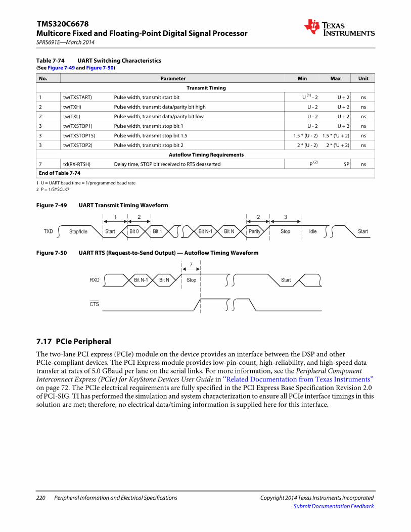
220 Peripheral Information and Electrical Specifications Copyright 2014 Texas Instruments Incorporated
SPRS691E—March 2014Multicore Fixed and Floating-Point Digital Signal ProcessorTMS320C6678
Submit Documentation Feedback
Figure 7-49 UART Transmit Timing Waveform
Figure 7-50 UART RTS (Request-to-Send Output) — Autoflow Timing Waveform
7.17 PCIe PeripheralThe two-lane PCI express (PCIe) module on the device provides an interface between the DSP and other PCIe-compliant devices. The PCI Express module provides low-pin-count, high-reliability, and high-speed data transfer at rates of 5.0 GBaud per lane on the serial links. For more information, see the Peripheral Component Interconnect Express (PCIe) for KeyStone Devices User Guide in ‘‘Related Documentation from Texas Instruments’’ on page 72. The PCIe electrical requirements are fully specified in the PCI Express Base Specification Revision 2.0 of PCI-SIG. TI has performed the simulation and system characterization to ensure all PCIe interface timings in this solution are met; therefore, no electrical data/timing information is supplied here for this interface.
Table 7-74 UART Switching Characteristics (See Figure 7-49 and Figure 7-50)
No. Parameter Min Max Unit
Transmit Timing
1 tw(TXSTART) Pulse width, transmit start bit U (1) - 2
1 U = UART baud time = 1/programmed baud rate
U + 2 ns
2 tw(TXH) Pulse width, transmit data/parity bit high U - 2 U + 2 ns
2 tw(TXL) Pulse width, transmit data/parity bit low U - 2 U + 2 ns
3 tw(TXSTOP1) Pulse width, transmit stop bit 1 U - 2 U + 2 ns
3 tw(TXSTOP15) Pulse width, transmit stop bit 1.5 1.5 * (U - 2) 1.5 * ('U + 2) ns
3 tw(TXSTOP2) Pulse width, transmit stop bit 2 2 * (U - 2) 2 * ('U + 2) ns
Autoflow Timing Requirements
7 td(RX-RTSH) Delay time, STOP bit received to RTS deasserted P (2)
2 P = 1/SYSCLK7
5P ns
End of Table 7-74
3221
Stop/IdleTXD Start Bit 0 Bit 1 Bit N-1 Bit N Parity Stop Idle Start
7
RXD Bit N-1 Bit N Stop Start
CTS
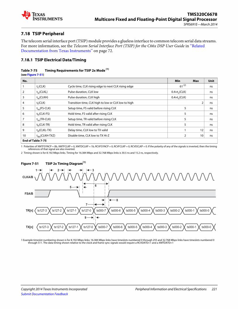
Multicore Fixed and Floating-Point Digital Signal Processor
Copyright 2014 Texas Instruments Incorporated Peripheral Information and Electrical Specifications 221
SPRS691E—March 2014
TMS320C6678
Submit Documentation Feedback
7.18 TSIP PeripheralThe telecom serial interface port (TSIP) module provides a glueless interface to common telecom serial data streams. For more information, see the Telecom Serial Interface Port (TSIP) for the C66x DSP User Guide in ‘‘Related Documentation from Texas Instruments’’ on page 72.
7.18.1 TSIP Electrical Data/Timing
Figure 7-51 TSIP 2x Timing Diagram(1)
1 Example timeslot numbering shown is for 8.192 Mbps links; 16.384 Mbps links have timeslots numbered 0 through 255 and 32.768 Mbps links have timeslots numbered 0 through 511. The data timing shown relative to the clock and frame sync signals would require a RCVDATD=1 and a XMTDATD=1
Table 7-75 Timing Requirements for TSIP 2x Mode (1)
(see Figure 7-51)
1 Polarities of XMTFSYNCP = 0b, XMTFCLKP = 0, XMTDCLKP = 1b, RCVFSYNCP = 0, RCVFCLKP = 0, RCVDCLKP = 0. If the polarity of any of the signals is inverted, then the timing references of that signal are also inverted.
No. Min Max Unit
1 tc(CLK) Cycle time, CLK rising edge to next CLK rising edge 61 (2)
2 Timing shown is for 8.192 Mbps links. Timing for 16.384 Mbps and 32.768 Mbps links is 30.5 ns and 15.2 ns, respectively.
ns
2 tw(CLKL) Pulse duration, CLK low 0.4×tc(CLK) ns
3 tw(CLKH) Pulse duration, CLK high 0.4×tc(CLK) ns
4 tt(CLK) Transition time, CLK high to low or CLK low to high 2 ns
5 tsu(FS-CLK) Setup time, FS valid before rising CLK 5 ns
6 th(CLK-FS) Hold time, FS valid after rising CLK 5 ns
7 tsu(TR-CLK) Setup time, TR valid before rising CLK 5 ns
8 th(CLK-TR) Hold time, TR valid after rising CLK 5 ns
9 td(CLKL-TX) Delay time, CLK low to TX valid 1 12 ns
10 tdis(CLKH-TXZ) Disable time, CLK low to TX Hi-Z 2 10 ns
End of Table 7-75
ts127-2ts127-3 ts127-0ts127-1 ts000-7 ts000-6 ts000-1ts000-3ts000-5 ts000-4 ts000-2 ts000-0
ts000-3ts127-2ts127-3 ts000-7ts127-1 ts127-0 ts000-5ts000-6 ts000-4 ts000-0ts000-2 ts000-1
CLKA/B
FSA/B
TR[n]
TX[n]
5
2
6
8
9
7
31

222 Peripheral Information and Electrical Specifications Copyright 2014 Texas Instruments Incorporated
SPRS691E—March 2014Multicore Fixed and Floating-Point Digital Signal ProcessorTMS320C6678
Submit Documentation Feedback
Figure 7-52 TSIP 1x Timing Diagram(1)
1 Example timeslot numbering shown is for 8.192 Mbps links; 16.384 Mbps links have timeslots numbered 0 through 255 and 32.768 Mbps links have timeslots numbered 0 through 511. The data timing shown relative to the clock and frame sync signals would require a RCVDATD=1023 and a XMTDATD=1023.
Table 7-76 Timing Requirements for TSIP 1x Mode (1)
(see Figure 7-52)
1 Polarities of XMTFSYNCP = 0b, XMTFCLKP = 0, XMTDCLKP = 0b, RCVFSYNCP = 0, RCVFCLKP = 0, RCVDCLKP = 1. If the polarity of any of the signals is inverted, then the timing references of that signal are also inverted.
No. Min Max Unit
11 tc(CLK) Cycle time, CLK rising edge to next CLK rising edge 122.1 (2)
2 Timing shown is for 8.192 Mbps links. Timing for 16.384 Mbps and 32.768 Mbps links is 61 ns and 30.5 ns, respectively.
ns
12 tw(CLKL) Pulse duration, CLK low 0.4×tc(CLK) ns
13 tw(CLKH) Pulse duration, CLK high 0.4×tc(CLK) ns
14 tt(CLK) Transition time, CLK high to low or CLK low to high 2 ns
15 tsu(FS-CLK) Setup time, FS valid before rising CLK 5 ns
16 th(CLK-FS) Hold time, FS valid after rising CLK 5 ns
17 tsu(TR-CLK) Setup time, TR valid before rising CLK 5 ns
18 th(CLK-TR) Hold time, TR valid after rising CLK 5 ns
19 td(CLKL-TX) Delay time, CLK low to TX valid 1 12 ns
20 tdis(CLKH-TXZ) Disable time, CLK low to TX Hi-Z 2 10 ns
End of Table 7-76
ts127-2ts127-3 ts127-0ts127-1 ts000-7 ts000-6 ts000-1ts000-3ts000-5 ts000-4 ts000-2 ts000-0
ts000-3ts127-2ts127-3 ts000-7ts127-1 ts127-0 ts000-5ts000-6 ts000-4 ts000-0ts000-2 ts000-1
11 12 13
15
16
1817
19
CLKA/B
FSA/B
TR[n]
TX[n]

Multicore Fixed and Floating-Point Digital Signal Processor
Copyright 2014 Texas Instruments Incorporated Peripheral Information and Electrical Specifications 223
SPRS691E—March 2014
TMS320C6678
Submit Documentation Feedback
7.19 EMIF16 PeripheralThe EMIF16 module provides an interface between DSP and external memories such as NAND and NOR flash. For more information, see the External Memory Interface (EMIF16) for KeyStone Devices User Guide in ‘‘Related Documentation from Texas Instruments’’ on page 72.
7.19.1 EMIF16 Electrical Data/Timing
Table 7-77 EMIF16 Asynchronous Memory Timing Requirements (1) (2)
(see Figure 7-53 and Figure 7-54)
No. Min Max Unit
General Timing
2 tw(WAIT) Pulse duration, WAIT assertion and deassertion minimum time 2E ns
28 td(WAIT-WEH) Setup time, WAIT asserted before WE high 4E + 3 ns
14 td(WAIT-OEH) Setup time, WAIT asserted before OE high 4E + 3 ns
Read Timing
3tC(CEL)
EMIF read cycle time when ew = 0, meaning not in extended wait mode (RS+RST+RH+3)*E-3
(RS+RST+RH+3)*E+3
ns
3tC(CEL)
EMIF read cycle time when ew =1, meaning extended wait mode enabled (RS+RST+WAIT+RH+3)* E-3
(RS+RST+WAIT+RH+3)* E+3
ns
4 tosu(CEL-OEL) Output setup time from CE low to OE low. SS = 0, not in select strobe mode (RS+1) * E - 3 (RS+1) * E + 3 ns
5 toh(OEH-CEH) Output hold time from OE high to CE high. SS = 0, not in select strobe mode (RH+1) * E - 3 (RH+1) * E + 3 ns
4 tosu(CEL-OEL) Output setup time from CE low to OE low in select strobe mode, SS = 1 (RS+1) * E - 3 (RS+1) * E + 3 ns
5 toh(OEH-CEH) Output hold time from OE high to CE high in select strobe mode, SS = 1 (RH+1) * E - 3 (RH+1) * E + 3 ns
6 tosu(BEV-OEL) Output setup time from BE valid to OE low (RS+1) * E - 3 (RS+1) * E + 3 ns
7 toh(OEH-BEIV) Output hold time from OE high to BE invalid (RH+1) * E - 3 (RH+1) * E + 3 ns
8 tosu(AV-OEL) Output setup time from A valid to OE low (RS+1) * E - 3 (RS+1) * E + 3 ns
9 toh(OEH-AIV) Output hold time from OE high to A invalid (RH+1) * E - 3 (RH+1) * E + 3 ns
10 tw(OEL) OE active time low, when ew = 0. Extended wait mode is disabled. (RST+1) * E - 3 (RST+1) * E + 3 ns
10 tw(OEL) OE active time low, when ew = 1. Extended wait mode is enabled. (RST+1) * E - 3 (RST+1) * E + 3 ns
11 td(WAITH-OEH) Delay time from WAIT deasserted to OE# high 4E + 3 ns
12 tsu(D-OEH) Input setup time from D valid to OE high 3 ns
13 th(OEH-D) Input hold time from OE high to D invalid 0.5 ns
Write Timing
15tc(CEL)
EMIF write cycle time when ew = 0, meaning not in extended wait mode (WS+WST+WH+3)* E-3
(WS+WST+WH+3)* E+3
ns
15tc(CEL)
EMIF write cycle time when ew =1., meaning extended wait mode is enabled (WS+WST+WAIT+WH+3)* E-3
(WS+WST+WAIT+WH+3)* E+3
ns
16 tosu(CEL-WEL) Output setup time from CE low to WE low. SS = 0, not in select strobe mode (WS+1) * E - 3 ns
17 toh(WEH-CEH) Output hold time from WE high to CE high. SS = 0, not in select strobe mode (WH+1) * E - 3 ns
16 tosu(CEL-WEL) Output setup time from CE low to WE low in select strobe mode, SS = 1 (WS+1) * E - 3 ns
17 toh(WEH-CEH) Output hold time from WE high to CE high in select strobe mode, SS = 1 (WH+1) * E - 3 ns
18 tosu(RNW-WEL) Output setup time from RNW valid to WE low (WS+1) * E - 3 ns
19 toh(WEH-RNW) Output hold time from WE high to RNW invalid (WH+1) * E - 3 ns
20 tosu(BEV-WEL) Output setup time from BE valid to WE low (WS+1) * E - 3 ns
21 toh(WEH-BEIV) Output hold time from WE high to BE invalid (WH+1) * E - 3 ns
22 tosu(AV-WEL) Output setup time from A valid to WE low (WS+1) * E - 3 ns
23 toh(WEH-AIV) Output hold time from WE high to A invalid (WH+1) * E - 3 ns

224 Peripheral Information and Electrical Specifications Copyright 2014 Texas Instruments Incorporated
SPRS691E—March 2014Multicore Fixed and Floating-Point Digital Signal ProcessorTMS320C6678
Submit Documentation Feedback
Figure 7-53 EMIF16 Asynchronous Memory Read Timing Diagram
Figure 7-54 EMIF16 Asynchronous Memory Write Timing Diagram
24 tw(WEL) WE active time low, when ew = 0. Extended wait mode is disabled. (WST+1) * E - 3 ns
24 tw(WEL) WE active time low, when ew = 1. Extended wait mode is enabled. (WST+1) * E - 3 ns
26 tosu(DV-WEL) Output setup time from D valid to WE low (WS+1) * E - 3 ns
27 toh(WEH-DIV) Output hold time from WE high to D invalid (WH+1) * E - 3 ns
25 td(WAITH-WEH) Delay time from WAIT deasserted to WE# high 4E + 3 ns
End of Table 7-77
1 E = 1/SYSCLK7, RS = Read Setup, RST = Read Strobe, RH = Read Hold, WS = Write Setup, WST = Write Strobe, WH = Write Hold.2 WAIT = number of cycles wait is asserted between the programmed end of the strobe period and wait de-assertion.
Table 7-77 EMIF16 Asynchronous Memory Timing Requirements (1) (2)
(see Figure 7-53 and Figure 7-54)
No. Min Max Unit
68
475
9
10
12 13
3
EMIFCE[3:0]
EMIFR/W
EMIFBE[1:0]
EMIFA[21:0]
EMIFOE
EMIFD[15:0]
EMIFWE
2022
18 2123
19
24
15
EMIFCE[3:0]
EMIFR/W
EMIFBE[1:0]
EMIFA[21:0]
EMIFWE
EMIFD[15:0]
EMIFOE
16
17
26
27

Multicore Fixed and Floating-Point Digital Signal Processor
Copyright 2014 Texas Instruments Incorporated Peripheral Information and Electrical Specifications 225
SPRS691E—March 2014
TMS320C6678
Submit Documentation Feedback
Figure 7-55 EMIF16 EM_WAIT Read Timing Diagram
Figure 7-56 EMIF16 EM_WAIT Write Timing Diagram
7.20 Packet AcceleratorThe packet accelerator provides L2 to L4 classification functionalities. It supports classification for Ethernet, VLAN, MPLS over Ethernet, IPv4/6, GRE over IP, and other session identification over IP such as TCP and UDP ports. It maintains 8K multiple-in, multiple-out hardware queues. It also provides checksum capability as well as some QoS capabilities. It enables a single IP address to be used for a multi-core device. It can process up to 1.5 M pps. The packet accelerator is coupled with the network coprocessor. For more information, see the Packet Accelerator (PA) for KeyStone Devices User Guide in ‘‘Related Documentation from Texas Instruments’’ on page 72.
7.21 Security AcceleratorThe security accelerator provides wire-speed processing on 1-Gbps Ethernet traffic on IPSec, SRTP, and 3GPP Air interface security protocols. It functions on the packet level with the packet and the associated security context being one of these above three types. The security accelerator is coupled with network coprocessor, and receives the packet descriptor containing the security context in the buffer descriptor, and the data to be encrypted/decrypted in the linked buffer descriptor. For more information, see the Security Accelerator (SA) for KeyStone Devices User Guide in ‘‘Related Documentation from Texas Instruments’’ on page 72.
14
EMIFCE[3:0]
EMIFOE
2
EMIFA[21:0]
EMIFBE[1:0]
EMIFD[15:0]
EMIFWAIT Asserted Deasserted
211
StrobeSetup Extended Due to EM_WAIT HoldStrobe
28
EMIFCE[3:0]
EMIFWE
2
EMIFA[21:0]
EMIFBE[1:0]
EMIFD[15:0]
EMIFWAIT Asserted Deasserted
225
StrobeSetup Extended Due to EM_WAIT HoldStrobe

226 Peripheral Information and Electrical Specifications Copyright 2014 Texas Instruments Incorporated
SPRS691E—March 2014Multicore Fixed and Floating-Point Digital Signal ProcessorTMS320C6678
Submit Documentation Feedback
7.22 Gigabit Ethernet (GbE) Switch SubsystemThe Gigabit Ethernet (GbE) switch subsystem provide an efficient interface between the TMS320C6678 DSP and the networked community. The GbE switch subsystem supports 10Base-T (10 Mbits/second [Mbps]), and 100BaseTX (100 Mbps), in half- or full-duplex mode, and 1000BaseT (1000 Mbps) in full-duplex mode, with hardware flow control and quality-of-service (QOS) support. The GbE switch subsystem is coupled with network coprocessor. For more information, see the Gigabit Ethernet (GbE) Switch Subsystem for KeyStone Devices User Guide in ‘‘Related Documentation from Texas Instruments’’ on page 72.
Each device has a unique MAC address. There are two registers to hold these values, MACID1 (0x02620110) and MACID2 (0x02620114). All bits of these registers are defined as follows:Figure 7-57 MACID1 Register
31 0
MACID[31:0]
R-xxxx xxxx xxxx xxxx xxxx xxxx xxxx xxxx
Legend: R = Read only; -x, value is indeterminate
Table 7-78 MACID1 Register Field Descriptions
Bit Field Description
31-0 MAC ID[31-0] MAC ID. A range will be assigned to this device. Each device will consume only one MAC address.
End of Table 7-78
Figure 7-58 MACID2 Register
31 24 23 18 17 16 15 0
Reserved Reserved FLOW BCAST MACID[47:32]
R-xxxx xxxx R-0 R-z R-y R-xxxx xxxx xxxx xxxx
Legend: R = Read only; -x, value is indeterminate
Table 7-79 MACID2 Register Field Descriptions
Bit Field Description
31-24 Reserved Reserved. Values will vary.
23-18 Reserved Reserved. Read as 0.
17 FLOW MAC flow control0 = Off1 = On
16 BCAST Default m/b-cast reception0 = Broadcast1 = Disabled
15-0 MAC ID[47-0] MAC ID
End of Table 7-79
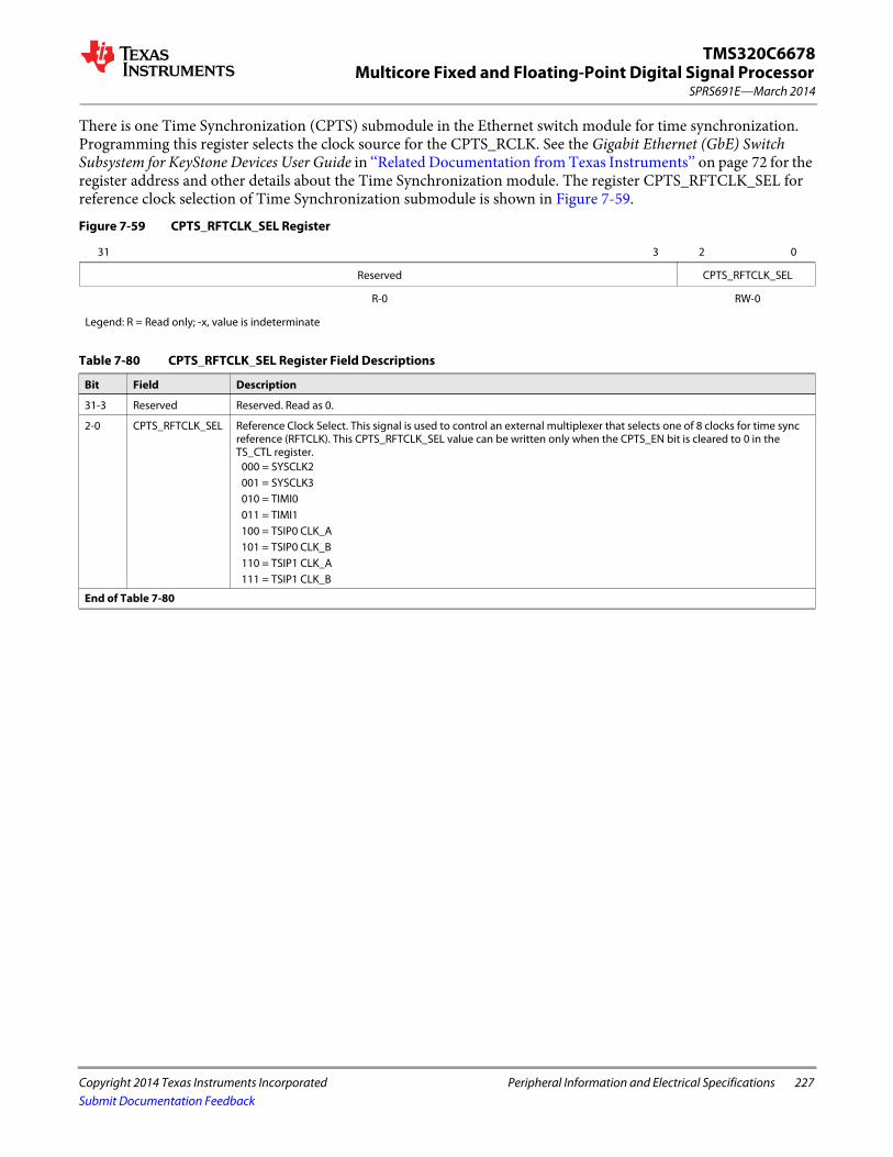
Multicore Fixed and Floating-Point Digital Signal Processor
Copyright 2014 Texas Instruments Incorporated Peripheral Information and Electrical Specifications 227
SPRS691E—March 2014
TMS320C6678
Submit Documentation Feedback
There is one Time Synchronization (CPTS) submodule in the Ethernet switch module for time synchronization. Programming this register selects the clock source for the CPTS_RCLK. See the Gigabit Ethernet (GbE) Switch Subsystem for KeyStone Devices User Guide in ‘‘Related Documentation from Texas Instruments’’ on page 72 for the register address and other details about the Time Synchronization module. The register CPTS_RFTCLK_SEL for reference clock selection of Time Synchronization submodule is shown in Figure 7-59.Figure 7-59 CPTS_RFTCLK_SEL Register
31 3 2 0
Reserved CPTS_RFTCLK_SEL
R-0 RW-0
Legend: R = Read only; -x, value is indeterminate
Table 7-80 CPTS_RFTCLK_SEL Register Field Descriptions
Bit Field Description
31-3 Reserved Reserved. Read as 0.
2-0 CPTS_RFTCLK_SEL Reference Clock Select. This signal is used to control an external multiplexer that selects one of 8 clocks for time sync reference (RFTCLK). This CPTS_RFTCLK_SEL value can be written only when the CPTS_EN bit is cleared to 0 in the TS_CTL register.
000 = SYSCLK2001 = SYSCLK3010 = TIMI0011 = TIMI1100 = TSIP0 CLK_A101 = TSIP0 CLK_B110 = TSIP1 CLK_A111 = TSIP1 CLK_B
End of Table 7-80
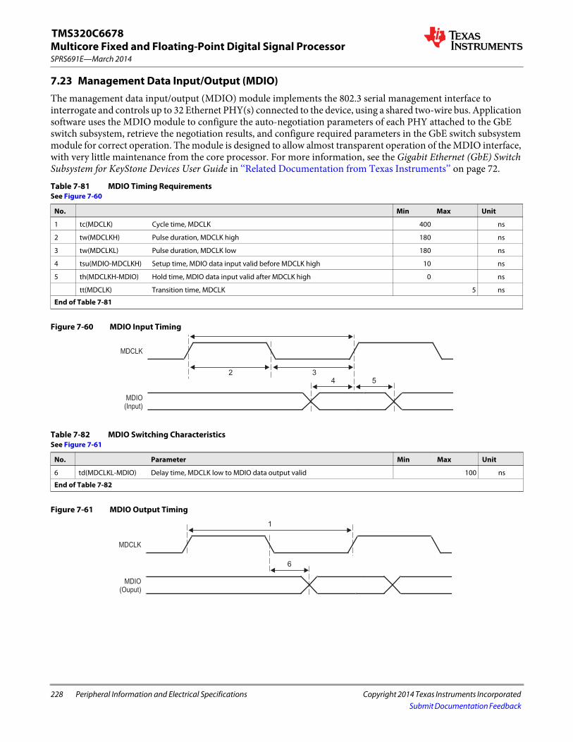
228 Peripheral Information and Electrical Specifications Copyright 2014 Texas Instruments Incorporated
SPRS691E—March 2014Multicore Fixed and Floating-Point Digital Signal ProcessorTMS320C6678
Submit Documentation Feedback
7.23 Management Data Input/Output (MDIO)The management data input/output (MDIO) module implements the 802.3 serial management interface to interrogate and controls up to 32 Ethernet PHY(s) connected to the device, using a shared two-wire bus. Application software uses the MDIO module to configure the auto-negotiation parameters of each PHY attached to the GbE switch subsystem, retrieve the negotiation results, and configure required parameters in the GbE switch subsystem module for correct operation. The module is designed to allow almost transparent operation of the MDIO interface, with very little maintenance from the core processor. For more information, see the Gigabit Ethernet (GbE) Switch Subsystem for KeyStone Devices User Guide in ‘‘Related Documentation from Texas Instruments’’ on page 72.
Figure 7-60 MDIO Input Timing
Figure 7-61 MDIO Output Timing
Table 7-81 MDIO Timing Requirements See Figure 7-60
No. Min Max Unit
1 tc(MDCLK) Cycle time, MDCLK 400 ns
2 tw(MDCLKH) Pulse duration, MDCLK high 180 ns
3 tw(MDCLKL) Pulse duration, MDCLK low 180 ns
4 tsu(MDIO-MDCLKH) Setup time, MDIO data input valid before MDCLK high 10 ns
5 th(MDCLKH-MDIO) Hold time, MDIO data input valid after MDCLK high 0 ns
tt(MDCLK) Transition time, MDCLK 5 ns
End of Table 7-81
Table 7-82 MDIO Switching CharacteristicsSee Figure 7-61
No. Parameter Min Max Unit
6 td(MDCLKL-MDIO) Delay time, MDCLK low to MDIO data output valid 100 ns
End of Table 7-82
MDIO(Input)
54
MDCLK
2 3
MDIO(Ouput)
1
6
MDCLK
Multicore Fixed and Floating-Point Digital Signal Processor
Copyright 2014 Texas Instruments Incorporated Peripheral Information and Electrical Specifications 229
SPRS691E—March 2014
TMS320C6678
Submit Documentation Feedback
7.24 TimersThe timers can be used to: time events, count events, generate pulses, interrupt the CPU and send synchronization events to the EDMA3 channel controller.
7.24.1 Timers Device-Specific Information
The TMS320C6678 device has sixteen 64-bit timers in total. Timer0 through Timer7 are dedicated to each of the eight CorePacs as a watchdog timer and can also be used as general-purpose timers. Each of the other eight timers can also be configured as a general-purpose timer only, with each timer programmed as a 64-bit timer or as two separate 32-bit timers.
When operating in 64-bit mode, the timer counts either VBUS clock cycles or input (TINPLx) pulses (rising edge) and generates an output pulse/waveform (TOUTLx) plus an internal event (TINTLx) on a software-programmable period.
When operating in 32-bit mode, the timer is split into two independent 32-bit timers. Each timer is made up of two 32-bit counters: a high counter and a low counter. The timer pins, TINPLx and TOUTLx are connected to the low counter. The timer pins, TINPHx and TOUTHx are connected to the high counter.
When operating in watchdog mode, the timer counts down to 0 and generates an event. It is a requirement that software writes to the timer before the count expires, after which the count begins again. If the count ever reaches 0, the timer event output is asserted. Reset initiated by a watchdog timer can be set by programming ‘‘Reset Type Status Register (RSTYPE)’’ on page 147 and the type of reset initiated can set by programming ‘‘Reset Configuration Register (RSTCFG)’’ on page 148. For more information, see the Timer64P for KeyStone Devices User Guide in ‘‘Related Documentation from Texas Instruments’’ on page 72.

230 Peripheral Information and Electrical Specifications Copyright 2014 Texas Instruments Incorporated
SPRS691E—March 2014Multicore Fixed and Floating-Point Digital Signal ProcessorTMS320C6678
Submit Documentation Feedback
7.24.2 Timers Electrical Data/Timing
The tables and figure below describe the timing requirements and switching characteristics of Timer0 through Timer15 peripherals.
Figure 7-62 Timer Timing
7.25 Serial RapidIO (SRIO) PortThe SRIO port on the TMS320C6678 device is a high-performance, low pin-count interconnect aimed for embedded markets. The use of the RapidIO interconnect in a baseband board design can create a homogeneous interconnect environment, providing even more connectivity and control among the components. RapidIO is based on the memory and device addressing concepts of processor buses where the transaction processing is managed completely by hardware. This enables the RapidIO interconnect to lower the system cost by providing lower latency, reduced overhead of packet data processing, and higher system bandwidth, all of which are key for wireless interfaces. For more information, see the Serial RapidIO (SRIO) for KeyStone Devices User Guide in ‘‘Related Documentation from Texas Instruments’’ on page 72.
Table 7-83 Timer Input Timing Requirements (1)
(see Figure 7-62)
1 C = 1/SYSCLK1 frequency in ns.
No. Min Max Unit
1 tw(TINPH) Pulse duration, high 12C ns
2 tw(TINPL) Pulse duration, low 12C ns
End of Table 7-83
Table 7-84 Timer Output Switching Characteristics (1)
(see Figure 7-62)
1 C = 1/SYSCLK1 frequency in ns.
No. Parameter Min Max Unit
3 tw(TOUTH) Pulse duration, high 12C - 3 ns
4 tw(TOUTL) Pulse duration, low 12C - 3 ns
End of Table 7-84
TIMIx
1 2
TIMOx
3 4

Multicore Fixed and Floating-Point Digital Signal Processor
Copyright 2014 Texas Instruments Incorporated Peripheral Information and Electrical Specifications 231
SPRS691E—March 2014
TMS320C6678
Submit Documentation Feedback
7.26 General-Purpose Input/Output (GPIO)7.26.1 GPIO Device-Specific Information
On the TMS320C6678, the GPIO peripheral pins GP[15:0] are also used to latch configuration pins. For more detailed information on device/peripheral configuration and the C6678 device pin muxing, see ‘‘Device Configuration’’ on page 73. For more information on GPIO, see the General Purpose Input/Output (GPIO) for KeyStone Devices User Guide ‘‘Related Documentation from Texas Instruments’’ on page 72.
7.26.2 GPIO Electrical Data/Timing
Figure 7-63 GPIO Timing
Table 7-85 GPIO Input Timing Requirements
No. Min Max Unit
1 tw(GPOH) Pulse duration, GPOx high 12C (1)
1 C = 1/SYSCLK1 frequency in ns.
ns
2 tw(GPOL) Pulse duration, GPOx low 12C ns
End of Table 7-85
Table 7-86 GPIO Output Switching Characteristics
No. Parameter Min Max Unit
3 tw(GPOH) Pulse duration, GPOx high 36C (1) - 8
1 C = 1/SYSCLK1 frequency in ns.
ns
4 tw(GPOL) Pulse duration, GPOx low 36C - 8 ns
End of Table 7-86
GPIx
1 2
GPOx
3 4
232 Peripheral Information and Electrical Specifications Copyright 2014 Texas Instruments Incorporated
SPRS691E—March 2014Multicore Fixed and Floating-Point Digital Signal ProcessorTMS320C6678
Submit Documentation Feedback
7.27 Semaphore2The device contains an enhanced semaphore module for the management of shared resources of the DSP C66x CorePacs. The semaphore enforces atomic accesses to shared chip-level resources so that the read-modify-write sequence is not broken. The semaphore block has unique interrupts to each of the cores to identify when that core has acquired the resource.
Semaphore resources within the module are not tied to specific hardware resources. It is a software requirement to allocate semaphore resources to the hardware resource(s) to be arbitrated.
The semaphore module supports 8 masters and contains 32 semaphores to be used within the system.
The semaphore module is accessible only by masters with privilege ID (privID) 0 to 7, which means only CorePac 0 to 7 or the EDMA transactions initiated by CorePac 0 to 7 can access the semaphore module.
If the remote device wants to access the semaphore module, the HyperLink configuration register must be appropriately configured, so the remote device can send transactions with the desired privID value to the local semaphore module. For more information on HyperLink configuration, see the HyperLink for KeyStone Devices User Guide in ‘‘Related Documentation from Texas Instruments’’ on page 72.
There are two methods of accessing a semaphore resource:• Direct Access: A core directly accesses a semaphore resource. If free, the semaphore will be granted. If not, the
semaphore is not granted.• Indirect Access: A core indirectly accesses a semaphore resource by writing it. Once it is free, an interrupt
notifies the CPU that it is available.
7.28 Emulation Features and Capability7.28.1 Advanced Event Triggering (AET)
The TMS320C6678 device supports advanced event triggering (AET). This capability can be used to debug complex problems as well as understand performance characteristics of user applications. AET provides the following capabilities:
• Hardware Program Breakpoints: specify addresses or address ranges that can generate events such as halting the processor or triggering the trace capture.
• Data Watchpoints: specify data variable addresses, address ranges, or data values that can generate events such as halting the processor or triggering the trace capture.
• Counters: count the occurrence of an event or cycles for performance monitoring.• State Sequencing: allows combinations of hardware program breakpoints and data watchpoints to precisely
generate events for complex sequences.
For more information on AET, see the following documents in ‘‘Related Documentation from Texas Instruments’’ on page 72:
• Using Advanced Event Triggering to Find and Fix Intermittent Real-Time Bugs application report• Using Advanced Event Triggering to Debug Real-Time Problems in High Speed Embedded Microprocessor
Systems application report
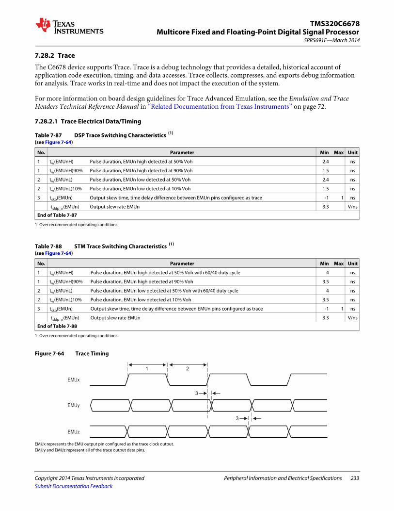
Multicore Fixed and Floating-Point Digital Signal Processor
Copyright 2014 Texas Instruments Incorporated Peripheral Information and Electrical Specifications 233
SPRS691E—March 2014
TMS320C6678
Submit Documentation Feedback
7.28.2 Trace
The C6678 device supports Trace. Trace is a debug technology that provides a detailed, historical account of application code execution, timing, and data accesses. Trace collects, compresses, and exports debug information for analysis. Trace works in real-time and does not impact the execution of the system.
For more information on board design guidelines for Trace Advanced Emulation, see the Emulation and Trace Headers Technical Reference Manual in ‘‘Related Documentation from Texas Instruments’’ on page 72.
7.28.2.1 Trace Electrical Data/Timing
Figure 7-64 Trace Timing
EMUx represents the EMU output pin configured as the trace clock output.EMUy and EMUz represent all of the trace output data pins.
Table 7-87 DSP Trace Switching Characteristics (1) (see Figure 7-64)
1 Over recommended operating conditions.
No. Parameter Min Max Unit
1 tw(EMUnH) Pulse duration, EMUn high detected at 50% Voh 2.4 ns
1 tw(EMUnH)90% Pulse duration, EMUn high detected at 90% Voh 1.5 ns
2 tw(EMUnL) Pulse duration, EMUn low detected at 50% Voh 2.4 ns
2 tw(EMUnL)10% Pulse duration, EMUn low detected at 10% Voh 1.5 ns
3 tsko(EMUn) Output skew time, time delay difference between EMUn pins configured as trace -1 1 ns
tsldp_(EMUn) Output slew rate EMUn 3.3 V/ns
End of Table 7-87
Table 7-88 STM Trace Switching Characteristics (1) (see Figure 7-64)
1 Over recommended operating conditions.
No. Parameter Min Max Unit
1 tw(EMUnH) Pulse duration, EMUn high detected at 50% Voh with 60/40 duty cycle 4 ns
1 tw(EMUnH)90% Pulse duration, EMUn high detected at 90% Voh 3.5 ns
2 tw(EMUnL) Pulse duration, EMUn low detected at 50% Voh with 60/40 duty cycle 4 ns
2 tw(EMUnL)10% Pulse duration, EMUn low detected at 10% Voh 3.5 ns
3 tsko(EMUn) Output skew time, time delay difference between EMUn pins configured as trace -1 1 ns
tsldp_(EMUn) Output slew rate EMUn 3.3 V/ns
End of Table 7-88
1
EMUx
EMUy
EMUz
2
3
3
234 Peripheral Information and Electrical Specifications Copyright 2014 Texas Instruments Incorporated
SPRS691E—March 2014Multicore Fixed and Floating-Point Digital Signal ProcessorTMS320C6678
Submit Documentation Feedback
7.28.3 IEEE 1149.1 JTAG
The JTAG interface is used to support boundary scan and emulation of the device. The boundary scan supported allows for an asynchronous TRST and only the 5 baseline JTAG signals (e.g., no EMU[1:0]) required for boundary scan. Most interfaces on the device follow the Boundary Scan Test Specification (IEEE1149.1), while all of the SerDes (SRIO and SGMII) support the AC-coupled net test defined in AC-Coupled Net Test Specification (IEEE1149.6).
It is expected that all compliant devices are connected through the same JTAG interface, in daisy-chain fashion, in accordance with the specification. The JTAG interface uses 1.8-V LVCMOS buffers, compliant with the Power Supply Voltage and Interface Standard for Nonterminated Digital Integrated Circuit Specification (EAI/JESD8-5).
7.28.3.1 IEEE 1149.1 JTAG Compatibility Statement
For maximum reliability, the C6678 DSP includes an internal pulldown (IPD) on the TRST pin to ensure that TRST will always be asserted upon power up and the DSP's internal emulation logic will always be properly initialized when this pin is not routed out. JTAG controllers from Texas Instruments actively drive TRST high. However, some third-party JTAG controllers may not drive TRST high but expect the use of an external pullup resistor on TRST. When using this type of JTAG controller, assert TRST to initialize the DSP after powerup and externally drive TRST high before attempting any emulation or boundary scan operations.
7.28.3.2 JTAG Electrical Data/Timing
Table 7-89 JTAG Test Port Timing Requirements (see Figure 7-65)
No. Min Max Unit
1 tc(TCK) Cycle time, TCK 34 ns
1a tw(TCKH) Pulse duration, TCK high (40% of tc) 13.6 ns
1b tw(TCKL) Pulse duration, TCK low(40% of tc) 13.6 ns
3 tsu(TDI-TCK) input setup time, TDI valid to TCK high 3.4 ns
3 tsu(TMS-TCK) input setup time, TMS valid to TCK high 3.4 ns
4 th(TCK-TDI) input hold time, TDI valid from TCK high 17 ns
4 th(TCK-TMS) input hold time, TMS valid from TCK high 17 ns
End of Table 7-89
Table 7-90 JTAG Test Port Switching Characteristics (1) (see Figure 7-65)
1 Over recommended operating conditions.
No. Parameter Min Max Unit
2 td(TCKL-TDOV) Delay time, TCK low to TDO valid 13.6 ns
End of Table 7-90

Multicore Fixed and Floating-Point Digital Signal Processor
Copyright 2014 Texas Instruments Incorporated Peripheral Information and Electrical Specifications 235
SPRS691E—March 2014
TMS320C6678
Submit Documentation Feedback
Figure 7-65 JTAG Test-Port Timing
TDI / TMS
1a
1
3
TCK
4
TDO
1b
2

236 Revision History Copyright 2014 Texas Instruments Incorporated
SPRS691E—March 2014Multicore Fixed and Floating-Point Digital Signal ProcessorTMS320C6678
Submit Documentation Feedback
8 Revision History
Revision EUpdated EDMA addressing mode descriptions. (Page 160)Updated BWADJ value setting description in MAIN/DDR3/PASS PLL registers (Page 150)Added info for output clocks to 1.8-V LVCMOS Signal Transition Levels paragraph (Page 120)Updated Main PLL and PLL Controller figure: removed /2 label from PLL object (Page 140)Updated Rise and Fall Transition Time Voltage Reference Levels figure to include label for lower transition (Page 120)Clarified SmartReflex pin output type (Page 53)Clarified table caption and first column heading (Page 167)Corrected SmartReflex peripheral I/O Buffer Type from LVCMOS category to Open drain (Page 119)Revised Main PLL Clock Input Transition Time figure (Page 152)Corrected EMIF16 Boot Device Configuration Bit Fields (Page 26)Added 1.4-GHz support for C6678 device across entire document (Page 1)Added GYP package to Device Characteristics table (Page 13)Added GYP package to Mechanical Data Chapter (Page 241)Restored Parameter Information section (Page 120)Updated Core Before IO Power Sequencing diagram, changing clock signal SYSCLK1P&N to REFCLK1P&N (Page 123)Updated IO Before Core Power Sequencing diagram, changing clock signal SYSCLK1P&N to REFCLK1P&N (Page 125)Updated the PASS PLL Block Diagram (Page 156)Updated the Trace timing diagram (Page 233)Updated Parameter Table Index bit field in I2C boot configuration (Page 29)Updated Parameter Table Index bit field in SPI boot configuration (Page 30)Updated PKTDMA_PRI_ALLOC register to be CHIP_MSIC_CTL register with new bit field added. (Page 77)Updated OUTPUT_DIVIDE default value and PLL clock formula in PLL Settings section (Page 38)Updated slow peripherals in SYSCLK7 description (Page 142)Updated Chip Select field description in SPI boot device configuration table (Page 30)Added DSP_SUSP_CTL register section (Page 77)
Revision DCorrected NMI7-0 from bit fields 23-16 to bit fields 15-8 in LRSTNMIPINSTAT and LRSTNMIPINSTAT_CLR registers (Page 80)Added Extended Boot Mode table in Boot Device Field section (Page 25)Updated event PO_VP_SMPSACK_INTR to be Reserved in CIC3 event table (Page 183)Updated Trace Electrical Timing tables and Timing diagrams (Page 233)Updated event PO_VCON_SMPSERR_INTR be Reserved in CIC0/1 Event Inputs table (Page 172)Added Boot Parameter Table section (Page 31)Added new section DDR3 Memory Controller Race Condition Consideration to include the last 3 paragraphs originally in section 7.11.1
(Page 205)Added REFCLK description in power sequencing section (Page 122)Added table of Bootloader section in L2 SRAM in Boot Sequence section (Page 23)Updated SYSCLK1 to REFCLK in power sequencing section to refer to the clock source of main PLL (Page 123)Updated note in power sequencing that each supply must ramp monotonically and must reach a stable valid level within 20 ms
(Page 123)Corrected differential clock rise and fall time in the PLL timing table for the clock inputs that feed into the LJCB clock buffers (Page 151)Changed all footnote references from CORECLK to SYSCLK1 (Page 231)Updated PCIe privilege level from "Supervisor" to "Driven by PCIe module" (Page 193)Corrected "Reserved" to be "Assert local reset to all CorePacs" in LRESET and NMI Decoding table (Page 189)Added MPU Registers Reset Values section (Page 203)Added "Initial Startup" row for CVDD in Recommended Operating Conditions table (Page 117)Added DDR3PLLCTL1 and PASSPLLCTL1 registers to Device Status Control Registers table (Page 76)Updated all SerDes clocks to discrete frequencies in the Clock Input Timing Requirements table (Page 151)Corrected tj(CORECLKN/P) max value from 100 to 0.02*tc(CORECLKN/P) (Page 151)Corrected tj(DDRCLKN/P) max value from 0.025*tc(DDRCLKN/P) to 0.02*tc(DDRCLKN/P) (Page 155)

Multicore Fixed and Floating-Point Digital Signal Processor
Copyright 2014 Texas Instruments Incorporated Revision History 237
SPRS691E—March 2014
TMS320C6678
Submit Documentation Feedback
Corrected tj(PASSCLKN/P) max value from 100 to 0.02*tc(PASSCLKN/P) (Page 158)Updated the descriptions of how Semaphore module is accessible (Page 232)Added Debug Subsystem Configuration region to memory map table (Page 19)Added HOUT timing diagram in Host Interrupt Output section (Page 191)Added note to DDR3 PLL initialization sequence (Page 154)Corrected MPU0 Memory Protection End Address from 0x026203FF to 0x026207FF (Page 192)Revised IPCGRH register description (Page 88)Corrected DDR3 transfer rate from 1033 MTS to 1066 MTS (Page 205)Added CVDD and SmartReflex voltage parameter in SmartReflex switching table (Page 128)Removed DDR3 PLL initialization sequence from data manual to PLL controller user guide (Page 154)Removed PASS PLL initialization sequence from data manual to PLL controller user guide (Page 157)Updated chip select from CS[5:2] to CE[3:0] in EMIF16 Peripheral section (Page 223)Updated EMIF chip select from CS[5:2] to CE[3:0] in Memory Map Summary table (Page 23)Updated DDR3 PLL initialization sequence (Page 155)Added footnote for DDR3 EMIF data in memory map summary table (Page 23)Updated Tracer descriptions across the data manual (Page 17)Corrected PASSCLK(N/P) max cycle time from 6.4 ns to 25 ns (Page 158)Updated the Timer numbering across the whole document (Page 18)Corrected PASS PLL clock to SRIOSGMIICLK in the boot device values table for Ethernet. (Page 25)Added clarification for RESETSTATz input current (Page 118)Added note for VCNTLID register that it is available for debug purpose only (Page 131)Added STM Trace Switching Characteristics table (Page 233)Removed the incorrect description of 16-Bit EMIF in Features section (Page 1)Updated th(MDCLKH-MDIO) value from 10 ns to 0 ns in MDIO Timing Requirements table (Page 228)Updated the description of NAND in the footnote of memory map summary table (Page 23)Updated tw(DPnH) and tw(DPnL) descriptions in Trace Switching Characteristics tables (Page 233)Updated I2C master mode table that bits[9:8] are used for mode selection (Page 28)Updated the I2C passive mode table that bits[9:8] are used for mode selection and actual value on the bus is 0x19+bits[7:5] (Page 29)Updated I2C data rate configuration descriptions in I2C Master Mode Configuration table (Page 28)Added PLLSELECT bit to PASSPLLCTL1 Register (Page 157)Added SPI device-specific support details (Page 212)Corrected that only the sticky bits in PCIe MMRs will be retained after soft reset (Page 136)
Revision CAdded note stating that both SGMII ports can be used for boot (Page 27)Updated the DDR3 MMR descriptions and deleted the unrelated PCIe MMR descriptions for soft reset. (Page 136)Corrected physical 36-bit addresses of DDR3 EMIF configuration/data (Page 23)Added TeraNet connection figures and added bridge numbers to the connection tables. (Page 99)Restricted Output Divide of SECCTL register to max value of divide by 2 (Page 144)Updated DEVSPEED register for both silicon rev1.0 and 2.0 (Page 96)Removed RESETFULLz parameter from 4b timing description (Page 124)Added supported data rates for HyperLink (Page 215)Changed chip level interrupt controller name from INTC to CIC (Page 165)Changed TPCC to EDMA3CC and TPTC to EDMA3TC (Page 159)Added PLLRST bit to DDR3PLLCTL1 register (Page 154)Added PLLRST bit to PASSPLLCTL1 register (Page 157)Deleted INTC0 register map address offset 0x4 and 0x8, which are Reserved (Page 183)Corrected the SGMII SerDes clock to PASS clock in PASS PLL configuration description (Page 38)Corrected PASS PLL clock from SRIOSGMIICLK to PASSCLK in the boot device values table for Ethernet. (Page 25)Corrected the SPI and DDR3/HyperLink Config end addressed (Page 23)Added the DDR3 PLL Initialization Sequence (Page 154)Added the Main PLL and PLL Controller Initialization Sequence (Page 151)Added the PASS PLL Initialization Sequence (Page 157)

238 Revision History Copyright 2014 Texas Instruments Incorporated
SPRS691E—March 2014Multicore Fixed and Floating-Point Digital Signal ProcessorTMS320C6678
Submit Documentation Feedback
Added HyperLink interrupt event section (Page 215)Added events #144-159 to INTC2 event input table (Page 178)Added DEVSPEED Register section. (Page 96)Added more description to Boot Sequence section (Page 23)Corrected a typo, changed DDRCLKN to DDRCLKP (Page 155)
Revision BRemoved section 7.1 Parameter Information (Page 120)Corrected PASS PLL clock source description from Main PLL mux to CORECLK clock reference sources (Page 156)Corrected MACID2 address from 0x02600114 to 0x02620114 (Page 226)Added EMIF16 Electrical Data/Timing section (Page 223)Added TSIP Electrical Data/Timing section (Page 221)Updated SPI Timing section (Page 212)Changed Data Rate 3 to Reserved from 12.5GBs in HyperLink configuration field table (Page 30)Corrected the Device ID field to be bits 5 to 3 in Ethernet Configuration Field figure and table (Page 27)Corrected the field bits of No Boot/EMIF16 configuration field figure and table (Page 26)
Revision AAdded note to RSISO register that both SRIOISO and SRISO will be set by boot ROM code during boot (Page 149)Removed AIF2ISO from Reset Isolation Register (Page 149)Added information of on-chip divider (=3) for PA in the PLL Boot Configuration Settings section (Page 38)Changed "no support for MSI" to "support for legacy INTx" for PCIe in legacy EP mode description in Device Status Register Field Descrip-
tions table (Page 78)Changed "no support for MSI" to "support for legacy INTx" for PCIe legacy end point description in Device Configuration Pins table
(Page 73)Added "The packet accelerator is coupled with network coprocessor" in the Packet Accelerator section (Page 225)Added Network Coprocessor document link (Page 72)Changed 2 to OUTPUT_DIVIDE in the clock formula in PLL Boot Configuration Settings section (Page 38)Changed EMAC to GbE switch subsystem (Page 226)Changed EMAC to Gigabit Ethernet (GbE) Switch Subsystem (Page 228)Changed EMAC to Gigabit Ethernet Switch (Page 72)Changed EMAC to Network Coprocessor Packet DMA (Page 98)Changed PA_SS into Network Coprocessor Packet DMA in Device Master Settings table (Page 192)Changed PA_SS into PASS in the Clock Sequencing table (Page 127)Changed Packet Accelerator into Network Coprocessor and corrected the memory address in the memory map summary table (Page 17)Changed Packet Accelerator into network coprocessor in Security Accelerator section (Page 225)Changed Packet Accelerator into Network Coprocessor in the Device Configuration Pins table. (Page 73)Changed Packet Accelerator subsystem into Network Coprocessor (Page 156)Changed Packet Subsystem to Network Coprocessor (PASS PLL) in Terminal Functions table (Page 44)Changed PASS into Network Coprocessor (PASS) (Page 141)Changed PS_SS_CLK PLL to PASS_CLK PLL in Terminal Functions table (Page 44)Deleted section 5.5 "C66x CorePac Resets" to avoid confusion and the reset details are covered in "Reset Controller" section (Page 108)Removed EMAC in Characteristics of the device Processor table (Page 13)Added BGA Package row into Characteristics of Processor table (Page 13)Corrected End and Bytes of DDR3 EMIF Configuration section in Memory Map Summary table (Page 17)Corrected BAR number from BAR1/2 to BAR2/3 and BAR3/4 to BAR4/5 in PCIe Window Sizes table (Page 28)Deleted EDMA3 Peripheral Register Description section, which is covered in EDMA user guide (Page 159)Added SerDes PLL Status and Config registers (Page 74)Added "to DDR3 memory space" to the first step of workaround (Page 205)Added "with TCCMOD=0" after "e.g. EDMA3 transfer controllers" (Page 205)Added CPTS_RFTCLK_SEL register in GbE Switch Subsystem section (Page 226)Changed "DSP/2" to "CPU/2" and "DSP/3" to "CPU/3" (Page 98)Changed the word "can" to "must" in the sentence "for most applications increment mode can be used" to specify it is a hard rule.
(Page 160)

Multicore Fixed and Floating-Point Digital Signal Processor
Copyright 2014 Texas Instruments Incorporated Revision History 239
SPRS691E—March 2014
TMS320C6678
Submit Documentation Feedback
Corrected the tw(RXSTOP15) and tw(RXSTOP2) values in UART Timing Requirements table (Page 219)Changed "sleep boot" to "No boot" in Sub-Mode field of No boot/EMIF16 Configuration Bit Field Descriptions table (Page 26)Changed Section 2.5.2.1 title from "Sleep/EMIF16" to "No Boot/EMIF16" (Page 26)Corrections Applied to I2C Passive Mode Device Configuration Bit Fields (Page 29)Corrections Applied to I2C Passive Mode Device Configuration Field Descriptions (Page 29)Modified description of value 0 to EMIF16/No Boot in Boot Device Values table (Page 25)Corrected SRIO configuration memory map from 0x02900000~0x02907FFF to 0x02900000~0x02920FFF (Page 17)Added thermal values into the Thermal Resistance Characteristics table. (Page 241)Added DDR3PLLCTL1 register and field description table (Page 154)Added more description to pin PTV15 in the Terminal Functions table (Page 45)Added PASSPLLCTL1 register and field descriptions (Page 157)Added Master ID Settings table. (Page 193)Added the table of Power Supply to Peripheral I/O Mapping (Page 119)Changed PROGn_MPEAR register table format and reset value format (Page 200)Changed PROGn_MPSAR registers table format and reset value format (Page 200)Modified the figure of SmartReflex 4-Pin VID Interface Timing (Page 128)Modified the table of SmartReflex 4-Pin VID Interface Switching Characteristics (Page 128)Added PROG4 registers set into MPU1 Registers table (Page 196)Changed number of programmable ranges supported from 4 to 5 for MPU1 (Page 192)Modified reset values in MPU Configuration Register table (Page 199)Modified Table 2-13 to include 1000 MHz and 1250 MHz columns. (Page 38)Added BWADJ[11:8] to MAINPLLCTL1 register table and description. (Page 150)Changed Privilege ID from the second column to the first column (Page 192)Changed PROG3_MPEA to PROG3_MPEAR in MPU1 Registers table (Page 196)Changed Programmable range enumeration from 1-N based to 0-N based in MPU Register Map. (Page 195)Changed SRIO_CPPI and SRIO_M rows to the single row (Page 192)Changed the master from Reserved to HyperLink with Privilege ID 13 and 14 (Page 192)Modified BWADJ descriptions in MAINPLLCTL0 and MAINPLLCTL1 registers (Page 150)Modified SECCTL register reference place in the note. (Page 151)Corrected Clock Sequencing table - Removed ALTCORECLK reference, Corrected SYSCLK as CORECLK. (Page 127)Corrections Applied to I2C Boot Device Configuration Bit Fields (Page 28)Corrections Applied to Sleep / EMIF16 Boot Device Configuration Bit Fields (Page 26)Updated Device Configuration Pins Table; PACLKSEL Functional Description (Page 73)Updated Reset Electrical Data / Timing section. Included updated reset requirements. (Page 138)Updated Reset Electrical Data; Included updated Reset Requirements. (Page 138)Updated Table 2-3 Boot Mode Pins: Boot Device Values description of the Ethernet (SGMII) boots. (Page 25)Removed the SRIOSMGIICLK, MCMCLK, and PCIECLK transition timing values with respect to VOH and VOL within the Main PLL Controller
timing requirements. (Page 151)Updated Terminal Descriptions of TSIP Pins (Page 54)Updated EMIF16 timing requirements table (Page 223)Added MAINPLLCTL1, Renamed DDR3PLLCTL0 to DDR3PLLCT, Renamed PAPLLCTL0 to PAPLLCTL (Page 74)Corrected the size of TETBs for the 4 cores from 16k to 4k (Page 17)Corrected the size of TETBs for the 4 cores from 16k to 4k (Page 17)Updated the complete Power-up sequencing section. RESETFULL must always de-assert after POR (Page 122)Added section NMI and LRSET. (Page 189)Corrected Extended Temperature range - Changed 105C to 100C for the top end. (Page 1)Added BWADJ bit field to DDR3 PLL Control Register. (Page 153)Added BWADJ bit field to PASS PLL Control Register. (Page 156)Added MAINPLLCTL1 register table and description. (Page 150)Added more detailed information on valid levels for CLKs and IOs during the power sequencing. (Page 122)Added Note on level interrupts and use of EOI handshaking. (Page 165)Corrected Address Range of I2C MMRs (Page 208)Corrected PACLKSEL bitfield description. (Page 78)
240 Revision History Copyright 2014 Texas Instruments Incorporated
SPRS691E—March 2014Multicore Fixed and Floating-Point Digital Signal ProcessorTMS320C6678
Submit Documentation Feedback
Corrected RSV01 should be pulled up to 1.8 V and RSV08 should be tied to GND (Page 55)Changed CVDD Range; Corrected CVDD and CVDD1 Descriptions (CVDD: Core Supply -> SR Core Supply) (CVDD1: SR Core Supply -> Core
Supply) (Page 117)Added more detailed information on valid levels for CLKs and IOs during the power sequencing. (Page 122)Added to table "Terminal Functions - Signals and Control by Function", signals - RSV0A and RSV0B. (Page 44)Corrected the timing pointers to point the correct figure (Page 138)Changed incorrect reserved address in Memory Map Summary - 02780400 -> 02778400 (Page 17)Corrected Commercial Temperature range - Changed 100C to 85C for the top end. (Page 1)

Multicore Fixed and Floating-Point Digital Signal Processor
Copyright 2014 Texas Instruments Incorporated Mechanical Data 241
SPRS691E—March 2014
TMS320C6678
Submit Documentation Feedback
9 Mechanical Data
9.1 Thermal DataTable 9-1 shows the thermal resistance characteristics for the CYP PBGA 841-pin package with Pb-free die bumps and Pb-free solder balls.
Table 9-2 shows the thermal resistance characteristics for the GYP PBGA 841-pin package with Pb-free die bumps and Pb-based solder balls.
9.2 Packaging InformationThe following packaging information reflects the most current released data available for the designated device(s). This data is subject to change without notice and without revision of this document.
Table 9-1 Thermal Resistance Characteristics for CYP (PBGA 841-Pin Package)
No. °C/W
1 RJC Junction-to-case 0.18
2 RJB Junction-to-board 3.71
End of Table 9-1
Table 9-2 Thermal Resistance Characteristics for GYP (PBGA 841-Pin Package)
No. °C/W
1 RJC Junction-to-case 0.18
2 RJB Junction-to-board 3.71
End of Table 9-2

242 Mechanical Data Copyright 2014 Texas Instruments Incorporated
SPRS691E—March 2014Multicore Fixed and Floating-Point Digital Signal ProcessorTMS320C6678
Submit Documentation Feedback
PACKAGE OPTION ADDENDUM
www.ti.com 21-Jul-2017
Addendum-Page 1
PACKAGING INFORMATION
Orderable Device Status(1)
Package Type PackageDrawing
Pins PackageQty
Eco Plan(2)
Lead/Ball Finish(6)
MSL Peak Temp(3)
Op Temp (°C) Device Marking(4/5)
Samples
SM320C6678ACYPW ACTIVE FCBGA CYP 841 44 Green (RoHS& no Sb/Br)
SNAGCU Level-4-245C-72HR -55 to 115 SM320C6678ACYP@2010 TIW
TMS320C6678ACYP ACTIVE FCBGA CYP 841 44 Green (RoHS& no Sb/Br)
SNAGCU Level-4-245C-72HR 0 to 85 TMS320C6678CYP@2010 TI
TMS320C6678ACYP25 ACTIVE FCBGA CYP 841 44 Green (RoHS& no Sb/Br)
SNAGCU Level-4-245C-72HR 0 to 85 TMS320C6678CYP@2010 TI1.25GHZ
TMS320C6678ACYP4 ACTIVE FCBGA CYP 841 44 Green (RoHS& no Sb/Br)
SNAGCU Level-4-245C-72HR 0 to 85 TMS320C6678CYP@2010 TI1.4GHZ
TMS320C6678ACYPA ACTIVE FCBGA CYP 841 44 Green (RoHS& no Sb/Br)
SNAGCU Level-4-245C-72HR -40 to 100 TMS320C6678CYP@2010 TIA
TMS320C6678ACYPA25 ACTIVE FCBGA CYP 841 44 Green (RoHS& no Sb/Br)
SNAGCU Level-4-245C-72HR -40 to 100 TMS320C6678CYP@2010 TIA1.25GHZ
TMS320C6678AGYPA ACTIVE FCBGA GYP 841 44 TBD SNPB Level-4-245C-72 HR -40 to 100 TMS320C6678GYP@2010 TIA
TMS320C6678AXCYP ACTIVE FCBGA CYP 841 44 Green (RoHS& no Sb/Br)
SNAGCU Level-4-245C-72HR 0 to 85 TMS320C6678XCYP@2010 TI
TMS320C6678AXCYP25 ACTIVE FCBGA CYP 841 44 Green (RoHS& no Sb/Br)
SNAGCU Level-4-245C-72HR 0 to 85 TMS320C6678XCYP@2010 TI1.25GHZ
TMS320C6678AXCYPA ACTIVE FCBGA CYP 841 44 Green (RoHS& no Sb/Br)
SNAGCU Level-4-245C-72HR -40 to 100 TMS320C6678XCYP@2010 TIA
(1) The marketing status values are defined as follows:ACTIVE: Product device recommended for new designs.LIFEBUY: TI has announced that the device will be discontinued, and a lifetime-buy period is in effect.NRND: Not recommended for new designs. Device is in production to support existing customers, but TI does not recommend using this part in a new design.PREVIEW: Device has been announced but is not in production. Samples may or may not be available.OBSOLETE: TI has discontinued the production of the device.

PACKAGE OPTION ADDENDUM
www.ti.com 21-Jul-2017
Addendum-Page 2
(2) RoHS: TI defines "RoHS" to mean semiconductor products that are compliant with the current EU RoHS requirements for all 10 RoHS substances, including the requirement that RoHS substancedo not exceed 0.1% by weight in homogeneous materials. Where designed to be soldered at high temperatures, "RoHS" products are suitable for use in specified lead-free processes. TI mayreference these types of products as "Pb-Free".RoHS Exempt: TI defines "RoHS Exempt" to mean products that contain lead but are compliant with EU RoHS pursuant to a specific EU RoHS exemption.Green: TI defines "Green" to mean the content of Chlorine (Cl) and Bromine (Br) based flame retardants meet JS709B low halogen requirements of <=1000ppm threshold. Antimony trioxide basedflame retardants must also meet the <=1000ppm threshold requirement.
(3) MSL, Peak Temp. - The Moisture Sensitivity Level rating according to the JEDEC industry standard classifications, and peak solder temperature.
(4) There may be additional marking, which relates to the logo, the lot trace code information, or the environmental category on the device.
(5) Multiple Device Markings will be inside parentheses. Only one Device Marking contained in parentheses and separated by a "~" will appear on a device. If a line is indented then it is a continuationof the previous line and the two combined represent the entire Device Marking for that device.
(6) Lead/Ball Finish - Orderable Devices may have multiple material finish options. Finish options are separated by a vertical ruled line. Lead/Ball Finish values may wrap to two lines if the finishvalue exceeds the maximum column width.
Important Information and Disclaimer:The information provided on this page represents TI's knowledge and belief as of the date that it is provided. TI bases its knowledge and belief on informationprovided by third parties, and makes no representation or warranty as to the accuracy of such information. Efforts are underway to better integrate information from third parties. TI has taken andcontinues to take reasonable steps to provide representative and accurate information but may not have conducted destructive testing or chemical analysis on incoming materials and chemicals.TI and TI suppliers consider certain information to be proprietary, and thus CAS numbers and other limited information may not be available for release.
In no event shall TI's liability arising out of such information exceed the total purchase price of the TI part(s) at issue in this document sold by TI to Customer on an annual basis.


IMPORTANT NOTICE
Texas Instruments Incorporated (TI) reserves the right to make corrections, enhancements, improvements and other changes to itssemiconductor products and services per JESD46, latest issue, and to discontinue any product or service per JESD48, latest issue. Buyersshould obtain the latest relevant information before placing orders and should verify that such information is current and complete.TI’s published terms of sale for semiconductor products (http://www.ti.com/sc/docs/stdterms.htm) apply to the sale of packaged integratedcircuit products that TI has qualified and released to market. Additional terms may apply to the use or sale of other types of TI products andservices.Reproduction of significant portions of TI information in TI data sheets is permissible only if reproduction is without alteration and isaccompanied by all associated warranties, conditions, limitations, and notices. TI is not responsible or liable for such reproduceddocumentation. Information of third parties may be subject to additional restrictions. Resale of TI products or services with statementsdifferent from or beyond the parameters stated by TI for that product or service voids all express and any implied warranties for theassociated TI product or service and is an unfair and deceptive business practice. TI is not responsible or liable for any such statements.Buyers and others who are developing systems that incorporate TI products (collectively, “Designers”) understand and agree that Designersremain responsible for using their independent analysis, evaluation and judgment in designing their applications and that Designers havefull and exclusive responsibility to assure the safety of Designers' applications and compliance of their applications (and of all TI productsused in or for Designers’ applications) with all applicable regulations, laws and other applicable requirements. Designer represents that, withrespect to their applications, Designer has all the necessary expertise to create and implement safeguards that (1) anticipate dangerousconsequences of failures, (2) monitor failures and their consequences, and (3) lessen the likelihood of failures that might cause harm andtake appropriate actions. Designer agrees that prior to using or distributing any applications that include TI products, Designer willthoroughly test such applications and the functionality of such TI products as used in such applications.TI’s provision of technical, application or other design advice, quality characterization, reliability data or other services or information,including, but not limited to, reference designs and materials relating to evaluation modules, (collectively, “TI Resources”) are intended toassist designers who are developing applications that incorporate TI products; by downloading, accessing or using TI Resources in anyway, Designer (individually or, if Designer is acting on behalf of a company, Designer’s company) agrees to use any particular TI Resourcesolely for this purpose and subject to the terms of this Notice.TI’s provision of TI Resources does not expand or otherwise alter TI’s applicable published warranties or warranty disclaimers for TIproducts, and no additional obligations or liabilities arise from TI providing such TI Resources. TI reserves the right to make corrections,enhancements, improvements and other changes to its TI Resources. TI has not conducted any testing other than that specificallydescribed in the published documentation for a particular TI Resource.Designer is authorized to use, copy and modify any individual TI Resource only in connection with the development of applications thatinclude the TI product(s) identified in such TI Resource. NO OTHER LICENSE, EXPRESS OR IMPLIED, BY ESTOPPEL OR OTHERWISETO ANY OTHER TI INTELLECTUAL PROPERTY RIGHT, AND NO LICENSE TO ANY TECHNOLOGY OR INTELLECTUAL PROPERTYRIGHT OF TI OR ANY THIRD PARTY IS GRANTED HEREIN, including but not limited to any patent right, copyright, mask work right, orother intellectual property right relating to any combination, machine, or process in which TI products or services are used. Informationregarding or referencing third-party products or services does not constitute a license to use such products or services, or a warranty orendorsement thereof. Use of TI Resources may require a license from a third party under the patents or other intellectual property of thethird party, or a license from TI under the patents or other intellectual property of TI.TI RESOURCES ARE PROVIDED “AS IS” AND WITH ALL FAULTS. TI DISCLAIMS ALL OTHER WARRANTIES ORREPRESENTATIONS, EXPRESS OR IMPLIED, REGARDING RESOURCES OR USE THEREOF, INCLUDING BUT NOT LIMITED TOACCURACY OR COMPLETENESS, TITLE, ANY EPIDEMIC FAILURE WARRANTY AND ANY IMPLIED WARRANTIES OFMERCHANTABILITY, FITNESS FOR A PARTICULAR PURPOSE, AND NON-INFRINGEMENT OF ANY THIRD PARTY INTELLECTUALPROPERTY RIGHTS. TI SHALL NOT BE LIABLE FOR AND SHALL NOT DEFEND OR INDEMNIFY DESIGNER AGAINST ANY CLAIM,INCLUDING BUT NOT LIMITED TO ANY INFRINGEMENT CLAIM THAT RELATES TO OR IS BASED ON ANY COMBINATION OFPRODUCTS EVEN IF DESCRIBED IN TI RESOURCES OR OTHERWISE. IN NO EVENT SHALL TI BE LIABLE FOR ANY ACTUAL,DIRECT, SPECIAL, COLLATERAL, INDIRECT, PUNITIVE, INCIDENTAL, CONSEQUENTIAL OR EXEMPLARY DAMAGES INCONNECTION WITH OR ARISING OUT OF TI RESOURCES OR USE THEREOF, AND REGARDLESS OF WHETHER TI HAS BEENADVISED OF THE POSSIBILITY OF SUCH DAMAGES.Unless TI has explicitly designated an individual product as meeting the requirements of a particular industry standard (e.g., ISO/TS 16949and ISO 26262), TI is not responsible for any failure to meet such industry standard requirements.Where TI specifically promotes products as facilitating functional safety or as compliant with industry functional safety standards, suchproducts are intended to help enable customers to design and create their own applications that meet applicable functional safety standardsand requirements. Using products in an application does not by itself establish any safety features in the application. Designers mustensure compliance with safety-related requirements and standards applicable to their applications. Designer may not use any TI products inlife-critical medical equipment unless authorized officers of the parties have executed a special contract specifically governing such use.Life-critical medical equipment is medical equipment where failure of such equipment would cause serious bodily injury or death (e.g., lifesupport, pacemakers, defibrillators, heart pumps, neurostimulators, and implantables). Such equipment includes, without limitation, allmedical devices identified by the U.S. Food and Drug Administration as Class III devices and equivalent classifications outside the U.S.TI may expressly designate certain products as completing a particular qualification (e.g., Q100, Military Grade, or Enhanced Product).Designers agree that it has the necessary expertise to select the product with the appropriate qualification designation for their applicationsand that proper product selection is at Designers’ own risk. Designers are solely responsible for compliance with all legal and regulatoryrequirements in connection with such selection.Designer will fully indemnify TI and its representatives against any damages, costs, losses, and/or liabilities arising out of Designer’s non-compliance with the terms and provisions of this Notice.
Mailing Address: Texas Instruments, Post Office Box 655303, Dallas, Texas 75265Copyright © 2017, Texas Instruments Incorporated