Embed Size (px)
Citation preview

www.ti.com
1 TMS320DM355 Digital Media System-on-Chip (DMSoC)
1.1 Features
TMS320DM355Digital Media System-on-Chip (DMSoC)SPRS463D–SEPTEMBER 2007–REVISED FEBRUARY 2008
• 8-/16-bit YCC and Up to 18-Bit RGB666• High-Performance Digital MediaDigital OutputSystem-on-Chip
• BT.601/BT.656 Digital YCbCr 4:2:2– 216- and 270-MHz ARM926EJ-S Clock Rate(8-/16-Bit) Interface– Fully Software-Compatible With ARM9
• Supports digital HDTV (720p/1080i)• ARM926EJ-S Core output for connection to external– Support for 32-Bit and 16-Bit (Thumb Mode) encoderInstruction Sets• External Memory Interfaces (EMIFs)– DSP Instruction Extensions and Single – DDR2 and mDDR SDRAM 16-bit wide EMIFCycle MAC With 256 MByte Address Space (1.8-V I/O)– ARM Jazelle Technology – Asynchronous16-/8-bit Wide EMIF (AEMIF)– EmbeddedICE-RT Logic for Real-Time
• Flash Memory InterfacesDebug– NAND (8-/16-bit Wide Data)• ARM9 Memory Architecture– OneNAND(16-bit Wide Data)– 16K-Byte Instruction Cache
• Flash Card Interfaces– 8K-Byte Data Cache– Two Multimedia Card (MMC) / Secure– 32K-Byte RAM Digital (SD/SDIO)– 8K-Byte ROM – SmartMedia– Little Endian
• Enhanced Direct-Memory-Access (EDMA)• MPEG4/JPEG Coprocessor Controller (64 Independent Channels)– Fixed Function Coprocessor Supports: • USB Port with Integrated 2.0 High-Speed PHY
• MPEG4 SP Codec at HD (720p), D1, that SupportsVGA, SIF – USB 2.0 Full and High-Speed Device
• JPEG Codec up to 50M Pixels per – USB 2.0 Low, Full, and High-Speed HostSecond• Three 64-Bit General-Purpose Timers (each• Video Processing Subsystem configurable as two 32-bit timers)
– Front End Provides: • One 64-Bit Watch Dog Timer• Hardware IPIPE for Real-Time Image
• Three UARTs (One fast UART with RTS andProcessing CTS Flow Control)• CCD and CMOS Imager Interface• Three Serial Port Interfaces (SPI) each with• 14-Bit Parallel AFE (Analog Front End) two Chip-SelectsInterface Up to 75 MHz• One Master/Slave Inter-Integrated Circuit• Glueless Interface to Common Video (I2C) Bus™Decoders• Two Audio Serial Port (ASP)• BT.601/BT.656 Digital YCbCr 4:2:2
– I2S and TDM I2S(8-/16-Bit) Interface– AC97 Audio Codec Interface• Histogram Module– S/PDIF via Software• Resize Engine– Standard Voice Codec Interface (AIC12)– Resize Images From 1/16x to 8x– SPI Protocol (Master Mode Only)– Separate Horizontal/Vertical Control
• Four Pulse Width Modulator (PWM) Outputs– Two Simultaneous Output Paths• Four RTO (Real Time Out) Outputs– Back End Provides:• Up to 104 General-Purpose I/O (GPIO) Pins• Hardware On-Screen Display (OSD)
(Multiplexed with Other Device Functions)• Composite NTSC/PAL video encoderoutput • On-Chip ARM ROM Bootloader (RBL) to Boot
Please be aware that an important notice concerning availability, standard warranty, and use in critical applications of TexasInstruments semiconductor products and disclaimers thereto appears at the end of this document.
I2C-bus is a trademark of Texas Instruments.Windows is a trademark of Microsoft.All other trademarks are the property of their respective owners.
PRODUCTION DATA information is current as of publication date. Copyright © 2007–2008, Texas Instruments IncorporatedProducts conform to specifications per the terms of the TexasInstruments standard warranty. Production processing does notnecessarily include testing of all parameters.

www.ti.com
TMS320DM355Digital Media System-on-Chip (DMSoC)SPRS463D–SEPTEMBER 2007–REVISED FEBRUARY 2008
From NAND Flash, MMC/SD, or UART – ETB (Embedded Trace Buffer) with4K-Bytes Trace Buffer memory• Configurable Power-Saving Modes
– Device Revision ID Readable by ARM• Crystal or External Clock Input (typically• 337-Pin Ball Grid Array (BGA) Package24 MHz or 36 MHz)
(ZCE Suffix), 0.65-mm Ball Pitch• Flexible PLL Clock Generators• 90nm Process Technology• Debug Interface Support• 3.3-V and 1.8-V I/O, 1.3-V Internal– IEEE-1149.1 (JTAG)
Boundary-Scan-Compatible
2 TMS320DM355 Digital Media System-on-Chip (DMSoC) Submit Documentation Feedback

www.ti.com
1.2 Description
TMS320DM355Digital Media System-on-Chip (DMSoC)SPRS463D–SEPTEMBER 2007–REVISED FEBRUARY 2008
The DM355 is a highly integrated, programmable platform for digital still camera, digital photo frames, IPsecurity cameras, 4-channel digital video recorders, video door bell application, and other low costportable digital video applications. Designed to offer portable video designers and manufacturers theability to produce affordable portable digital video solutions with high picture quality, the DM355 combineshigh performance MPEG4 HD (720p) codecs and JPEG codecs up to 50M pixels per second, high quality,and low power consumption at a very low price point. The DM355 also enables seamless interface to mostadditional external devices required for a complete digital camera implementation. The interface is flexibleenough to support various types of CCD and CMOS sensors, signal conditioning circuits, powermanagement, DDR/mDDR memory, SRAM, NAND, shutter, Iris and auto-focus motor controls, etc.
The DM355 processor core is an ARM926EJ-S RISC processor. The ARM926EJ-S is a 32-bit processorcore that performs 32-bit and 16-bit instructions and processes 32-bit, 16-bit, and 8-bit data. The coreuses pipelining so that all parts of the processor and memory system can operate continuously. The ARMcore incorporates:• A coprocessor 15 (CP15) and protection module• Data and program Memory Management Units (MMUs) with table look-aside buffers.• Separate 16K-byte instruction and 8K-byte data caches. Both are four-way associative with virtual
index virtual tag (VIVT).
DM355 performance is enhanced by its MPEG4/JPEG coprocessor. The MPEG4/JPEG coprocessorperforms the computational operations required for image processing; JPEG compression and MPEG4video and imaging standard. The MPEG4/JPEG coprocessor supports MPEG4 SP at HD (720p), D1,VGA, SIF encode/decode resolutions and JPEG encode/decode up to 50M pixels per second.
The DM355 device has a Video Processing Subsystem (VPSS) with two configurable video/imagingperipherals:• A Video Processing Front-End (VPFE)• A Video Processing Back-End (VPBE)
The VPFE port provides an interface for CCD/CMOS imager modules and video decoders. The VPBEprovides hardware On Screen Display (OSD) support and composite NTSC/PAL and digital LCD output.
The DM355 peripheral set includes:• An inter-integrated circuit (I2C) Bus interface• Two audio serial ports (ASP)• Three 64-bit general-purpose timers each configurable as two independent 32-bit timers• A 64-bit watchdog timer• Up to 104-pins of general-purpose input/output (GPIO) with programmable interrupt/event generation
modes, multiplexed with other peripherals• Three UARTs with hardware handshaking support on one UART• Three serial port Interfaces (SPI)• Four pulse width modulator (PWM) peripherals• Four real time out (RTO) outputs• Two Multi-Media Card / Secure Digital (MMC/SD) interfaces• A USB 2.0 full and high-speed device and host interface• Two external memory interfaces:
– An asynchronous external memory interface (AEMIF) for slower memories/peripherals such asNAND and OneNAND,
– A high speed synchronous memory interface for DDR2/mDDR.
Submit Documentation Feedback TMS320DM355 Digital Media System-on-Chip (DMSoC) 3

www.ti.com
1.3 Functional Block Diagram
Peripherals64bit DMA/Data Bus
JTAG 24 MHzor 36 MHz
27 MHz(optional)
CCD/CMOSModule
DDR2/mDDR 16
CLOCK
PLLCLOCK ctrl
PLLs
JTAJTAGI/F
Clocks
ARM
z )
ARM926EJ-S_Z8
I-cach
e16 K
B
l-cache16KB
B
RA
M32 K
B
RAM32KB
BD-
cach
e8KD-cache
8KB
RO
M8 KROM8KB
CCD
C
3AH3A
DMA /Data and configuration busDMA/Data and configuration bus
DDR
MH
z )
DDRcontroller
DLDLL/PHY
16 bit
32bit Configuration Bus
CCDCIPIPE
VPBE
Vide
oEncod
er
VideoEncoder
10bDAC OS
D
OSD
erc
ARMARM INTC
Enhanced
channels3PCC /TC
(100 MHz
Enhanced DMA64 channels
Composite video
Digital RGB/YUV
Nand /Nand/SM/Async/One Nand
(AEMIF)
USB 2.0USB2.0 PHY
Speakermicrophone
ASP (2x)
Bu
ffer
Lo
gic
VPSS
MMC/SD (x2)
SPI I/F (x3)
UART (x3)
I2C
Timer/WDT (x4 - 64)
GIO
PWM (x4)
RTO
VPFE
Enhanced
channels3PCC /TC
(100 MHz
MPEG4/JPEGCoprocessor
TMS320DM355Digital Media System-on-Chip (DMSoC)SPRS463D–SEPTEMBER 2007–REVISED FEBRUARY 2008
For software development support the DM355 has a complete set of ARM development tools whichinclude: C compilers, assembly optimizers to simplify programming and scheduling, and a Windows™debugger interface for visibility into source code execution.
Figure 1-1 shows the functional block diagram of the DM355 device.
Figure 1-1. Functional Block Diagram
TMS320DM355 Digital Media System-on-Chip (DMSoC)4 Submit Documentation Feedback

www.ti.com
Contents
TMS320DM355Digital Media System-on-Chip (DMSoC)SPRS463D–SEPTEMBER 2007–REVISED FEBRUARY 2008
1 TMS320DM355 Digital Media System-on-Chip 4.2 Recommended Operating Conditions............... 92(DMSoC) ................................................... 1 4.3 Electrical Characteristics Over Recommended
Ranges of Supply Voltage and Operating Case1.1 Features .............................................. 1Temperature (Unless Otherwise Noted) ............ 931.2 Description............................................ 3
5 DM355 Peripheral Information and Electrical1.3 Functional Block Diagram ............................ 4 Specifications ........................................... 942 Device Overview ......................................... 6
5.1 Parameter Information Device-Specific Information 942.1 Device Characteristics................................ 6 5.2 Recommended Clock and Control Signal Transition2.2 Memory Map Summary............................... 7 Behavior ............................................. 962.3 Pin Assignments...................................... 9 5.3 Power Supplies...................................... 962.4 Pin Functions........................................ 13 5.4 Reset ................................................ 982.5 Pin List .............................................. 36 5.5 Oscillators and Clocks............................... 992.6 Device Support ...................................... 55 5.6 General-Purpose Input/Output (GPIO)............. 104
3 Detailed Device Description.......................... 59 5.7 External Memory Interface (EMIF)................. 1063.1 ARM Subsystem Overview.......................... 59 5.8 MMC/SD ........................................... 1133.2 ARM926EJ-S RISC CPU............................ 60 5.9 Video Processing Sub-System (VPSS) Overview . 1153.3 Memory Mapping.................................... 62 5.10 USB 2.0 ............................................ 1273.4 ARM Interrupt Controller (AINTC)................... 63 5.11 Universal Asynchronous Receiver/Transmitter
(UART) ............................................. 1293.5 Device Clocking ..................................... 655.12 Serial Port Interface (SPI).......................... 1313.6 PLL Controller (PLLC)............................... 735.13 Inter-Integrated Circuit (I2C) ....................... 1343.7 Power and Sleep Controller (PSC).................. 775.14 Audio Serial Port (ASP)............................ 1373.8 System Control Module ............................. 775.15 Timer ............................................... 1453.9 Pin Multiplexing...................................... 785.16 Pulse Width Modulator (PWM)..................... 1463.10 Device Reset ........................................ 795.17 Real Time Out (RTO) .............................. 1483.11 Default Device Configurations....................... 805.18 IEEE 1149.1 JTAG ................................ 1493.12 Device Boot Modes ................................. 83
6 Revision History (Revision D)...................... 1523.13 Power Management................................. 857 Mechanical Data....................................... 1533.14 64-Bit Crossbar Architecture ........................ 87
7.1 Thermal Data for ZCE ............................. 1533.15 MPEG4/JPEG Overview ............................ 907.1.1 Packaging Information............................. 1534 Device Operating Conditions ........................ 91
4.1 Absolute Maximum Ratings Over Operating CaseTemperature Range(Unless Otherwise Noted) .......................... 91
Submit Documentation Feedback Contents 5

www.ti.com
2 Device Overview
2.1 Device Characteristics
TMS320DM355Digital Media System-on-Chip (DMSoC)SPRS463D–SEPTEMBER 2007–REVISED FEBRUARY 2008
Table 2-1 provides an overview of the DMSoC. The table shows significant features of the device,including the peripherals, capacity of on-chip RAM, ARM operating frequency, the package type with pincount, etc.
Table 2-1. Characteristics of the ProcessorHARDWARE FEATURES DM355
DDR2 / mDDR Memory Controller DDR2 / mDDR (16-bit bus width)Asynchronous (8/16-bit bus width)Asynchronous EMIF (AEMIF) RAM, Flash (NAND, OneNAND)
Two MMC/SDFlash Card Interfaces One SmartMedia/xD64 independent DMA channelsEDMA Eight EDMA channels
Three 64-Bit General Purpose (eachconfigurable as two separate 32-bitTimers timers)Peripherals
One 64-Bit Watch DogNot all peripherals pins are
Three (one with RTS and CTS flowavailable at the same time UART control)(For more detail, see theDevice Configuration Three (each supports two slaveSPIsection). devices)
I2C One (Master/Slave)Audio Serial Port [ASP] Two ASPGeneral-Purpose Input/Output Port Up to 104Pulse width modulator (PWM) Four outputs
One Input (VPFE)Configurable Video Ports One Output (VPBE)High, Full Speed DeviceUSB 2.0 High, Full, Low Speed Host
ARMOn-Chip CPU Memory Organization 16-KB I-cache, 8-KB D-cache,
32-KB RAM, 8-KB ROMJTAG BSDL_ID JTAGID register (address location: 0x01C4 0028) 0x0B73B01FCPU Frequency (Maximum) MHz ARM 216 MHz and 270 MHz
Core (V) 1.3 VVoltage
I/O (V) 3.3 V, 1.8 VReference frequency options 24 MHz (typical), 36 MHzPLL Options Configurable PLL controller PLL bypass, programmable PLL
BGA Package 13 x 13 mm 337-Pin BGA (ZCE)Process Technology 90 nm
Product Preview (PP),Product Status (1) Advance Information (AI), PD
or Production Data (PD)
(1) PRODUCTION DATA information is current as of publication date. Products conform to specifications per the terms of the TexasInstruments standard warranty. Production processing does not necessarily include testing of all parameters.
Device Overview6 Submit Documentation Feedback
www.ti.com
2.2 Memory Map Summary
TMS320DM355Digital Media System-on-Chip (DMSoC)SPRS463D–SEPTEMBER 2007–REVISED FEBRUARY 2008
Table 2-3 shows the memory map address ranges of the device. Table 2-3 depicts the expanded map ofthe Configuration Space (0x01C0 0000 through 0x01FF FFFF). The device has multiple on-chip memoriesassociated with its processor and various subsystems. To help simplify software development a unifiedmemory map is used where possible to maintain a consistent view of device resources across all busmasters. The bus masters are the ARM, EDMA, USB, and VPSS.
Table 2-2. DM355 Memory MapStart Address End Address Size (Bytes) ARM EDMA USB VPSS
Mem Map Mem Map Mem Map Mem Map0x0000 0000 0x0000 3FFF 16K ARM RAM0
(Instruction)0x0000 4000 0x0000 7FFF 16K ARM RAM1 Reserved Reserved(Instruction)0x0000 8000 0x0000 FFFF 32K ARM ROM
(Instruction)- only 8K used
0x0001 0000 0x0001 3FFF 16K ARM RAM0 (Data) ARM RAM0 ARM RAM00x0001 4000 0x0001 7FFF 16K ARM RAM1 (Data) ARM RAM1 ARM RAM10x0001 8000 0x0001 FFFF 32K ARM ROM (Data) ARM ROM ARM ROM
- only 8K used0x0002 0000 0x000F FFFF 896K Reserved0x0010 0000 0x01BB FFFF 26M0x01BC 0000 0x01BC 0FFF 4K ARM ETB Mem0x01BC 1000 0x01BC 17FF 2K ARM ETB Reg Reserved0x01BC 1800 0x01BC 18FF 256 ARM IceCrusher Reserved0x01BC 1900 0x01BC FFFF 59136 Reserved0x01BD 0000 0x01BF FFFF 192K0x01C0 0000 0x01FF FFFF 4M CFG Bus CFG Bus ReservedPeripherals Peripherals0x0200 0000 0x09FF FFFF 128M ASYNC EMIF (Data) ASYNC EMIF (Data)0x0A00 0000 0x11EF FFFF 127M - 16K0x11F0 0000 0x11F1 FFFF 128K Reserved Reserved0x11F2 0000 0x1FFF FFFF 141M-64K0x2000 0000 0x2000 7FFF 32K DDR EMIF Control DDR EMIF Control
Regs Regs0x2000 8000 0x41FF FFFF 544M-32K Reserved0x4200 0000 0x49FF FFFF 128M Reserved AEMIF - shadow0x4A00 0000 0x7FFF FFFF 864M Reserved0x8000 0000 0x8FFF FFFF 256M DDR EMIF DDR EMIF DDR EMIF DDR EMIF0x9000 0000 0xFFFF FFFF 1792M Reserved Reserved Reserved Reserved
Table 2-3. DM355 ARM Configuration Bus Access to PeripheralsAddress Accessibility
Region Start End Size ARM EDMAEDMA CC 0x01C0 0000 0x01C0 FFFF 64K √ √
EDMA TC0 0x01C1 0000 0x01C1 03FF 1K √ √
EDMA TC1 0x01C1 0400 0x01C1 07FF 1K √ √
Reserved 0x01C1 8800 0x01C1 9FFF 6K √ √
Reserved 0x01C1 A000 0x01C1 FFFF 24K √ √
UART0 0x01C2 0000 0x01C2 03FF 1K √ √
Submit Documentation Feedback Device Overview 7

www.ti.com
TMS320DM355Digital Media System-on-Chip (DMSoC)SPRS463D–SEPTEMBER 2007–REVISED FEBRUARY 2008
Table 2-3. DM355 ARM Configuration Bus Access to Peripherals (continued)Address Accessibility
UART1 0x01C2 0400 0x01C2 07FF 1K √ √
Timer4/5 0x01C2 0800 0x01C2 0BFF 1K √ √
Real-time out 0x01C2 0C00 0x01C2 0FFF 1K √ √
I2C 0x01C2 1000 0x01C2 13FF 1K √ √
Timer0/1 0x01C2 1400 0x01C2 17FF 1K √ √
Timer2/3 0x01C2 1800 0x01C2 1BFF 1K √ √
WatchDog Timer 0x01C2 1C00 0x01C2 1FFF 1K √ √
PWM0 0x01C2 2000 0x01C2 23FF 1K √ √
PWM1 0x01C2 2400 0x01C2 27FF 1K √ √
PWM2 0x01C2 2800 0x01C2 2BFF 1K √ √
PWM3 0x01C2 2C00 0x01C2 2FFF 1K √ √
System Module 0x01C4 0000 0x01C4 07FF 2K √ √
PLL Controller 0 0x01C4 0800 0x01C4 0BFF 1K √ √
PLL Controller 1 0x01C4 0C00 0x01C4 0FFF 1K √ √
Power/Sleep Controller 0x01C4 1000 0x01C4 1FFF 4K √ √
ARM Interrupt Controller 0x01C4 8000 0x01C4 83FF 1K √ √
USB OTG 2.0 Regs / RAM 0x01C6 4000 0x01C6 5FFF 8K √ √
SPI0 0x01C6 6000 0x01C6 67FF 2K √ √
SPI1 0x01C6 6800 0x01C6 6FFF 2K √ √
GPIO 0x01C6 7000 0x01C6 77FF 2K √ √
SPI2 0x01C6 7800 0x01C6 FFFF 2K √ √
VPSS Subsystem 0x01C7 0000 0x01C7 FFFF 64K √ √
VPSS Clock Control 0x01C7 0000 0x01C7 007F 128 √ √
Hardware 3A 0x01C7 0080 0x01C7 00FF 128 √ √
Image Pipe (IPIPE) Interface 0x01C7 0100 0x01C7 01FF 256 √ √
On Screen Display 0x01C7 0200 0x01C7 02FF 256 √ √
High Speed Serial IF 0x01C7 0300 0x01C7 03FF 256 √ √
Video Encoder 0x01C7 0400 0x01C7 05FF 512 √ √
CCD Controller 0x01C7 0600 0x01C7 07FF 256 √ √
VPSS Buffer Logic 0x01C7 0800 0x01C7 08FF 256 √ √
Reserved 0x01C7 0900 0x01C7 09FF 256 √ √
Image Pipe (IPIPE) 0x01C7 1000 0x01C7 3FFF 12K √ √
Reserved 0x01CC 0000 0x01CD FFFF 128K √ √
Multimedia / SD 1 0x01E0 0000 0x01E0 1FFF 8K √ √
ASP0 0x01E0 2000 0x01E0 3FFF 8K √ √
ASP1 0x01E0 4000 0x01E0 5FFF 8K √ √
UART2 0x01E0 6000 0x01E0 63FF 1K √ √
Reserved 0x01E0 6400 0x01E0 FFFF 39K √ √
ASYNC EMIF Control 0x01E1 0000 0x01E1 0FFF 4K √ √
Multimedia / SD 0 0x01E1 1000 0x01E1 FFFF 60K √ √
Reserved 0x01E2 0000 0x01FF FFFF 1792K √ √
ASYNC EMIF Data (CE0) 0x0200 0000 0x03FF FFFF 32M √ √
ASYNC EMIF Data (CE1) 0x0400 0000 0x05FF FFFF 32M √ √
Reserved 0x0A00 0000 0x0BFF FFFF 32M √ √
Reserved 0x0C00 0000 0x0FFF FFFF 64M √ √
Device Overview8 Submit Documentation Feedback

www.ti.com
2.3 Pin Assignments
2.3.1 Pin Map (Bottom View)
9
J
8
VSSA_PLL2
7
VDDA33_USB
65431
H
G
VDDA13_USB
VSS
F
E
D
CIN2
C
B
A
VREFCIN3CIN0
VDDA_PLL2VSSLCD_OEFIELDVCLKVSS
VSSCVDDVSYNCEXTCLKVFB
VDD_VOUTVDD_VOUTVDD_VOUTHSYNCCOUT0COUT1TVOUT
TDOEMU0EMU1VSS_USBUSB_VBUSCOUT2COUT3IOUT
TDITMSVSS_USBUSB_IDCOUT4VSS
TRSTVSS_USB_REFUSB_R1VDDD13_USBUSB_DRV
VBUSCVDDYOUT7COUT5
MXO1VSSVSS_USBVDDA33_USB_
PLLVSSYOUT5YOUT4YOUT0
MXI1VSSUSB_DPUSB_DMVSSYOUT6YOUT2CVDD
2
VSS
VSS
VSS
IBIAS
VSS
COUT6
COUT7
YOUT3
YOUT1
RSV01
VDD
VDD
NC
TMS320DM355Digital Media System-on-Chip (DMSoC)SPRS463D–SEPTEMBER 2007–REVISED FEBRUARY 2008
Extensive use of pin multiplexing is used to accommodate the largest number of peripheral functions inthe smallest possible package. Pin multiplexing is controlled using a combination of hardwareconfiguration at device reset and software programmable register settings.
Figure 2-1 through Figure 2-4 show the pin assignments in four quadrants (A, B, C, and D). Note thatmicro-vias are not required. Contact your TI representative for routing recommendations.
Figure 2-1. Pin Map [Quadrant A]
Submit Documentation Feedback Device Overview 9

www.ti.com
W
9
DDR_CLK
8
DDR_CLK
7654
DDR_A05
32
DDR_A02
1
V DDR_A07DDR_A04DDR_A00
U VSS
T PCLK
R
P
N
M
L
K
DDR_A11DDR_A09DDR_A08VSS
DDR_CASDDR_BA[2]DDR_A12DDR_A10DDR_A01VSS
DDR_BA[0]DDR_BA[1]DDR_A13DDR_A06
DDR_A03
VSSVSSVSSVSS
DDR_ZNDDR_CSDDR_RASVSSVSSMXO2
VDD_DDRCVDDCVDDVSSCAM_WEN_FIELD
CAM_VDYIN3VSSMXI2
VDD_DDRVDD_VINYIN0YIN2YIN4YIN1VSS_MX2
VSSVSSCVDDCAM_HDCIN7RSV05VSS
VDD_DDRVSSVSSVSSYIN5YIN6CIN5RSV06RSV04
VSSVSS_DACVDDA18V_DACVDDYIN7CIN4CIN1VSSRSV03
VSSVDDCVDDCIN6VSSRSV07RSV02
VDD_VINVDD_VIN
TMS320DM355Digital Media System-on-Chip (DMSoC)SPRS463D–SEPTEMBER 2007–REVISED FEBRUARY 2008
Figure 2-2. Pin Map [Quadrant B]
Device Overview10 Submit Documentation Feedback

www.ti.com
CVDD
19
W
18
DDR_DQGATE0
17
DDR_DQ15
16
DDR_DQ13
15
DDR_DQ11
14
DDR_DQ10
13
DDR_DQ07
12
DDR_DQ05
11
DDR_DQ01
10
DDR_WE
EM_A13 VVSSDDR_
DQGATE1DDR_DQ14DDR_DQS[1]DDR_DQ09DDR_DQ06DDR_DQS[0]DDR_DQ00DDR_CKE
EM_A12 UUART0_RXDVSSDDR_DQ12DDR_DQM[1]VSSDDR_DQ08DDR_DQ04DDR_DQ02DDR_VREF
EM_A08 TUART0_TXDCVDDVSSVDD_DDRDDR_DQM[0]DDR_DQ03
EM_A05 REM_A10UART1_TXDEM_A11UART1_RXDI2C_SCLI2C_SDAVDD_DDRVSSA_DLLVDDA33_DDRDLL
EM_BA1 PEM_A06EM_A09EM_A07EM_A04VDD_DDR
EM_BA0 NEM_A03EM_A01EM_A02VSSVDDVDD
EM_D14 MEM_D15VSSEM_A00EM_D13VSSVDD
EM_D10 LEM_D12EM_D11EM_D08EM_D04CVDDVSS
EM_D07 KEM_D09EM_D06
VDD_DDR VDD_DDR VDD_DDR VDD_DDR
VDDVDDVDD
CVDD VDD
VSS CVDD CVDD
VSS
VSS VDD
TMS320DM355Digital Media System-on-Chip (DMSoC)SPRS463D–SEPTEMBER 2007–REVISED FEBRUARY 2008
Figure 2-3. Pin Map [Quadrant C]
Submit Documentation Feedback Device Overview 11

www.ti.com
19181716151413121110
EM_D05 J
EM_D02 H
EM_CE1 G
F
E
D
C
VDD
B
A
EM_D03EM_D01EM_CE0EM_WEVSS
EM_D00EM_ADVASP0_DXVSSA_PLL1CVDD
EM_WAITASP0_FSXGIO003VDDA_PLL1
EM_OEASP0_CLKXASP0_CLKRASP0_FSRGIO002
EM_CLKASP0_DRASP1_FSRASP1_FSXGIO001SPI1_
SDENA[0]SPI1_SDORTCKTCK
ASP1_CLKXASP1_CLKRASP1_CLKSGIO005MMCSD0_
DATA1CLKOUT1RESET
ASP1_DRASP1_DXGIO007GIO000MMCSD1_CLKMMCSD0_CMDSPI1_SCLKSPI0_SCLKCLKOUT3VSS_MX1
GIO006
MMCSD1_DATA0
MMCSD1_DATA3
MMCSD1_DATA2
GIO004
MMCSD1_CMD
MMCSD1_DATA1
MMCSD0_CLK
MMCSD0_DATA0
MMCSD0_DATA3
MMCSD0_DATA2
SPI1_SDI
SPI0_SDENA[0]
SPI0_SDI
SPI0_SDO
CLKOUT2
VSS
CVDD CVDD CVDD VSS
CVDD VSS CVDD
CVDD
VDDVDDVDDVDDVDD
VSS
CVDDVSS
VSSCVDD
TMS320DM355Digital Media System-on-Chip (DMSoC)SPRS463D–SEPTEMBER 2007–REVISED FEBRUARY 2008
Figure 2-4. Pin Map [Quadrant D]
Device Overview12 Submit Documentation Feedback
www.ti.com
2.4 Pin Functions
2.4.1 Image Data Input - Video Processing Front End
TMS320DM355Digital Media System-on-Chip (DMSoC)SPRS463D–SEPTEMBER 2007–REVISED FEBRUARY 2008
The pin functions tables (Table 2-4 through Table 2-22) identify the external signal names, the associatedpin (ball) numbers along with the mechanical package designator, the pin type, whether the pin has anyinternal pullup or pulldown resistors, and a functional pin description. For more detailed information ondevice configuration, peripheral selection, multiplexed/shared pins, and debugging considerations, seeSection 3. For the list of all pin in chronological order see Section 2.5
The CCD Controller module in the Video Processing Front End has an external signal interface for imagedata input. It supports YUV (YC) inputs as well as Bayer RGB and complementary input signals (I.e.,image data input).
The definition of the CCD controller data input signals depend on the input mode selected.• In 16-bit YCbCr mode, the Cb and Cr signals are multiplexed on the Cl signals and the order is
configurable (i.e., Cb first or Cr first).• In 8-bit YCbCr mode, the Y, Cb, and Cr signals are multiplexed and not only is the order selectable,
but also the half of the bus used.
Table 2-4. CCD Controller Signals for Each Input ModePIN NAME CCD 16-BIT YCbCr 8-BIT YCbCr
Cl7 Cb7,Cr7 Y7,Cb7,Cr7Cl6 Cb6,Cr6 Y6,Cb6,Cr6Cl5 CCD13 Cb5,Cr5 Y5,Cb5,Cr5Cl4 CCD12 Cb4,Cr4 Y4,Cb4,Cr4Cl3 CCD11 Cb3,Cr3 Y3,Cb3,Cr3Cl2 CCD10 Cb2,Cr2 Y2,Cb2,Cr2Cl1 CCD9 Cb1,Cr1 Y1,Cb1,Cr1Cl0 CCD8 Cb0,Cr0 Y0,Cb0,Cr0Yl7 CCD7 Y7 Y7,Cb7,Cr7Yl6 CCD6 Y6 Y6,Cb6,Cr6Yl5 CCD5 Y5 Y5,Cb5,Cr5Yl4 CCD4 Y4 Y4,Cb4,Cr4Yl3 CCD3 Y3 Y3,Cb3,Cr3Yl2 CCD2 Y2 Y2,Cb2,Cr2Yl1 CCD1 Y1 Y1,Cb1,Cr1Yl0 CCD0 Y0 Y0,Cb0,Cr0
Submit Documentation Feedback Device Overview 13

www.ti.com
TMS320DM355Digital Media System-on-Chip (DMSoC)SPRS463D–SEPTEMBER 2007–REVISED FEBRUARY 2008
Table 2-5. CCD Controller/Video Input Terminal FunctionsTERMINAL
TYPE (1) OTHER (2) (3) DESCRIPTIONNAME NO.
Standard CCD Analog Front End (AFE): NOT USED• YCC 16-bit: Time multiplexed between chroma: CB/SR[07]CIN7/ PD • YCC 8-bit (which allows for two simultaneous decoder inputs), it is timeGIO101/ N3 I/O/Z VDD_VIN multiplexed between luma and chroma of the upper channel. Y/CB/CR[07]SPI2_SCLKSPI: SPI2 ClockGIO: GIO[101]Standard CCD Analog Front End (AFE): NOT USED• YCC 16-bit: Time multiplexed between chroma: CB/SR[06]CIN6/ PD • YCC 8-bit (which allows for two simultaneous decoder inputs), it is timeGIO100/ K5 I/O/Z VDD_VIN multiplexed between luma and chroma of the upper channel. Y/CB/CR[06]SPI2_SDOSPI: SPI2 Data OutGIO: GIO[100]Standard CCD Analog Front End (AFE): Raw[13]
CIN5/ • YCC 16-bit: Time multiplexed between chroma: CB/SR[05]GIO099/ PD • YCC 8-bit (which allows for two simultaneous decoder inputs), it is timeM3 I/O/ZSPI2_SDEN VDD_VIN multiplexed between luma and chroma of the upper channel. Y/CB/CR[05]A[0] SPI: SPI2 Chip Select
GIO: GIO[099]Standard CCD Analog Front End (AFE): Raw[12]
CIN4/ • YCC 16-bit: Time multiplexed between chroma: CB/SR[04]GIO098/ PD • YCC 8-bit (which allows for two simultaneous decoder inputs), it is timeL4 I/O/ZSPI2_SDEN VDD_VIN multiplexed between luma and chroma of the upper channel. Y/CB/CR[04]A[1] SPI: SPI2 Data In
GIO: GIO[098]Standard CCD Analog Front End (AFE): Raw[11]• YCC 16-bit: Time multiplexed between chroma: CB/SR[03]CIN3/ PDJ4 I/O/Z • YCC 8-bit (which allows for two simultaneous decoder inputs), it is timeGIO097/ VDD_VIN multiplexed between luma and chroma of the upper channel. Y/CB/CR[03]GIO: GIO[097]Standard CCD Analog Front End (AFE): Raw[10]• YCC 16-bit: Time multiplexed between chroma: CB/SR[02]CIN2/ PDJ5 I/O/Z • YCC 8-bit (which allows for two simultaneous decoder inputs), it is timeGIO096/ VDD_VIN multiplexed between luma and chroma of the upper channel. Y/CB/CR[02]GIO: GIO[097]Standard CCD Analog Front End (AFE): Raw[09]• YCC 16-bit: Time multiplexed between chroma: CB/SR[01]CIN1/ PDL3 I/O/Z • YCC 8-bit (which allows for two simultaneous decoder inputs), it is timeGIO095/ VDD_VIN multiplexed between luma and chroma of the upper channel. Y/CB/CR[01]GIO: GIO[095]Standard CCD Analog Front End (AFE): Raw[08]• YCC 16-bit: Time multiplexed between chroma: CB/SR[00]CIN0/ PDJ3 I/O/Z • YCC 8-bit (which allows for two simultaneous decoder inputs), it is timeGIO094/ VDD_VIN multiplexed between luma and chroma of the upper channel. Y/CB/CR[00]GIO: GIO[094]Standard CCD Analog Front End (AFE): Raw[07]• YCC 16-bit: Time multiplexed between chroma: Y[07]YIN7/ PDL5 I/O/Z • YCC 8-bit (which allows for two simultaneous decoder inputs), it is timeGIO093 VDD_VIN multiplexed between luma and chroma of the upper channel. Y/CB/CR[07]GIO: GIO[093]Standard CCD Analog Front End (AFE): Raw[06]• YCC 16-bit: Time multiplexed between chroma: Y[06]YIN6/ PDM4 I/O/Z • YCC 8-bit (which allows for two simultaneous decoder inputs), it is timeGIO092 VDD_VIN multiplexed between luma and chroma of the upper channel. Y/CB/CR[06]GIO: GIO[092]
(1) I = Input, O = Output, Z = High impedance, S = Supply voltage, GND = Ground, A = Analog signal.(2) PD = internal pull-down, PU = internal pull-up. (To pull up a signal to the opposite supply rail, a 1 kΩ resistor should be used.)(3) Specifies the operating I/O supply voltage for each signal. See Section 5.3, Power Supplies for more detail.
Device Overview14 Submit Documentation Feedback

www.ti.com
2.4.2 Image Data Output - Video Processing Back End (VPBE)
TMS320DM355Digital Media System-on-Chip (DMSoC)SPRS463D–SEPTEMBER 2007–REVISED FEBRUARY 2008
Table 2-5. CCD Controller/Video Input Terminal Functions (continued)TERMINAL
TYPE (1) OTHER (2) (3) DESCRIPTIONNAME NO.
Standard CCD Analog Front End (AFE): Raw[05]• YCC 16-bit: Time multiplexed between chroma: Y[05]YIN5/ PDM5 I/O/Z • YCC 8-bit (which allows for two simultaneous decoder inputs), it is timeGIO091 VDD_VIN multiplexed between luma and chroma of the upper channel. Y/CB/CR[05]GIO: GIO[091]Standard CCD Analog Front End (AFE): Raw[04]• YCC 16-bit: Time multiplexed between chroma: Y[04]YIN4/ PDP3 I/O/Z • YCC 8-bit (which allows for two simultaneous decoder inputs), it is timeGIO090 VDD_VIN multiplexed between luma and chroma of the upper channel. Y/CB/CR[04]GIO: GIO[090]Standard CCD Analog Front End (AFE): Raw[03]• YCC 16-bit: Time multiplexed between chroma: Y[03]YIN3/ PDR3 I/O/Z • YCC 8-bit (which allows for two simultaneous decoder inputs), it is timeGIO089 VDD_VIN multiplexed between luma and chroma of the upper channel. Y/CB/CR[03]GIO: GIO[089]Standard CCD Analog Front End (AFE): Raw[02]• YCC 16-bit: Time multiplexed between chroma: Y[02]YIN2/ PDP4 I/O/Z • YCC 8-bit (which allows for two simultaneous decoder inputs), it is timeGIO088 VDD_VIN multiplexed between luma and chroma of the upper channel. Y/CB/CR[02]GIO: GIO[088]Standard CCD Analog Front End (AFE): Raw[01]• YCC 16-bit: Time multiplexed between chroma: Y[01]YIN1/ PDP2 I/O/Z • YCC 8-bit (which allows for two simultaneous decoder inputs), it is timeGIO087 VDD_VIN multiplexed between luma and chroma of the upper channel. Y/CB/CR[01]GIO: GIO[087]Standard CCD Analog Front End (AFE): Raw[00]• YCC 16-bit: Time multiplexed between chroma: Y[00]YIN0/ PDP5 I/O/Z • YCC 8-bit (which allows for two simultaneous decoder inputs), it is timeGIO086 VDD_VIN multiplexed between luma and chroma of the upper channel. Y/CB/CR[00]GIO: GIO[086]Horizontal synchronization signal that can be either an input (slave mode) or anCAM_HD/ PDN5 I/O/Z output (master mode). Tells the CCDC when a new line starts.GIO085 VDD_VIN GIO: GIO[085]Vertical synchronization signal that can be either an input (slave mode) or an outputCAM_VD PDR4 I/O/Z (master mode). Tells the CCDC when a new frame starts.GIO084 VDD_VIN GIO: GIO[084]Write enable input signal is used by external device (AFE/TG) to gate the DDRoutput of the CCDC module. Alternately, the field identification input signal is usedCAM_WEN PD by external device (AFE/TG) to indicate which of two frames is input to the CCDC_FIELD\ R5 I/O/Z VDD_VIN module for sensors with interlaced output. CCDC handles 1- or 2-field sensors inGIO083 hardware.GIO: GIO[083]
PCLK/ PD Pixel clock input (strobe for lines C17 through Y10)T3 I/O/ZGIO082 VDD_VIN GIO: GIO[0082]
The Video Encoder/Digital LCD interface module in the video processing back end has an external signalinterface for digital image data output as described in Table 2-7 and Table 2-8.
The digital image data output signals support multiple functions / interfaces, depending on the displaymode selected. The following table describes these modes. Parallel RGB mode with more than RGB565signals requires enabling pin multiplexing to support (i.e., for RGB666 mode).
Submit Documentation Feedback Device Overview 15

www.ti.com
TMS320DM355Digital Media System-on-Chip (DMSoC)SPRS463D–SEPTEMBER 2007–REVISED FEBRUARY 2008
Table 2-6. Signals for VPBE Display ModesPIN NAME YCC16 YCC8/ PRGB SRGB
REC656HSYNC HSYNC HSYNC HSYNC HSYNCGIO073VSYNC VSYNC VSYNC VSYNC VSYNCGIO072LCD_OE As needed As needed As needed As neededGIO071FIELD As needed As needed As needed As needed
GIO070R2
PWM3CEXTCLK As needed As needed As needed As neededGIO069
B2PWM3DVCLK VCLK VCLK VCLK VCLK
GIO068YOUT7 Y7 Y7,Cb7,Cr7 R7 Data7YOUT6 Y6 Y6,Cb6,Cr6 R6 Data6YOUT5 Y5 Y5,Cb5,Cr5 R5 Data5YOUT4 Y4 Y4,Cb4,Cr4 R4 Data4YOUT3 Y3 Y3,Cb3,Cr3 R3 Data3YOUT2 Y2 Y2,Cb2,Cr2 G7 Data2YOUT1 Y1 Y1,Cb1,Cr1 G6 Data1YOUT0 Y0 Y0,Cb0,Cr0 G5 Data0COUT7 C7 LCD_AC G4 LCD_ACGIO081PWM0COUT6 C6 LCD_OE G3 LCD_OEGIO080PWM1COUT5 C5 BRIGHT G2 BRIGHTGIO079PWM2ARTO0
COUT4 C4 PWM B7 PWMGIO078PWM2BRTO1
COUT3 C3 CSYNC B6 CSYNCGIO077PWM2CRTO2
COUT2 C2 - B5 -GIO076PWM2DRTO3
COUT1 C1 - B4 -GIO075PWM3ACOUT0 C0 - B3 -GIO074PWM3B
Device Overview16 Submit Documentation Feedback

www.ti.com
TMS320DM355Digital Media System-on-Chip (DMSoC)SPRS463D–SEPTEMBER 2007–REVISED FEBRUARY 2008
Table 2-7. Digital Video Terminal FunctionsTERMINAL
TYPE (1) OTHER (2) (3) DESCRIPTION (4)NAME NO.YOUT7-R7 C3 I/O/Z VDD_VOUT Digital Video Out: VENC settings determine functionYOUT6-R6 A4 I/O/Z VDD_VOUT Digital Video Out: VENC settings determine functionYOUT5-R5 B4 I/O/Z VDD_VOUT Digital Video Out: VENC settings determine functionYOUT4-R4 B3 I/O/Z VDD_VOUT Digital Video Out: VENC settings determine functionYOUT3-R3 B2 I/O/Z VDD_VOUT Digital Video Out: VENC settings determine functionYOUT2-G7 A3 I/O/Z VDD_VOUT Digital Video Out: VENC settings determine functionYOUT1-G6 A2 I/O/Z VDD_VOUT Digital Video Out: VENC settings determine functionYOUT0-G5 B1 I/O/Z VDD_VOUT Digital Video Out: VENC settings determine functionCOUT7-G4/GIO081 C2 I/O/Z VDD_VOUT Digital Video Out: VENC settings determine function GIO: GIO[081] PWM0/PWM0COUT6-G3/GIO080 D2 I/O/Z VDD_VOUT Digital Video Out: VENC settings determine function GIO: GIO[080] PWM1/PWM1COUT5-G2/ GIO079 / C1 I/O/Z VDD_VOUT Digital Video Out: VENC settings determine function GIO: GIO[079] PWM2A RTO0PWM2A /RTO0COUT4-B7 /GIO078 / D3 I/O/Z VDD_VOUT Digital Video Out: VENC settings determine function GIO: GIO[078] PWM2B RTO1PWM2B /RTO1COUT3-B6 /GIO077 / E3 I/O/Z VDD_VOUT Digital Video Out: VENC settings determine function GIO: GIO[077] PWM2C RTO2PWM2C /RTO2COUT2-B5 /GIO076 / E4 I/O/Z VDD_VOUT Digital Video Out: VENC settings determine function GIO: GIO[076] PWM2D RTO3PWM2D /RTO3COUT1-B4 / Digital Video Out: VENC settings determine functionGIO075 / F3 I/O/Z VDD_VOUT GIO: GIO[075]PWM3A PWM3ACOUT0-B3 / Digital Video Out: VENC settings determine functionGIO074 / F4 I/O/Z VDD_VOUT GIO: GIO[074]PWM3B PWM3BHSYNC / PD Video Encoder: Horizontal SyncF5 I/O/ZGIO073 VDD_VOUT GIO: GIO[073]VSYNC / PD Video Encoder: Vertical SyncG5 I/O/ZGIO072 VDD_VOUT GIO: GIO[072]FIELD / Video Encoder: Field identifier for interlaced display formatsGIO070 / GIO: GIO[070]H4 I/O/Z VDD_VOUTR2 / Digital Video Out: R2PWM3C PWM3C
Video Encoder: External clock input, used if clock rates > 27 MHz are needed, e.g.EXTCLK / 74.25 MHz for HDTV digital outputGIO069 / PDG3 I/O/Z GIO: GIO[069]B2 / VDD_VOUT Digital Video Out: B2PWM3D PWM3DVCLK / Video Encoder: Video Output ClockH3 I/O/Z VDD_VOUTGIO068 GIO: GIO[068]
(1) I = Input, O = Output, Z = High impedance, S = Supply voltage, GND = Ground, A = Analog signal.(2) Specifies the operating I/O supply voltage for each signal. See Section 5.3, Power Supplies for more detail.(3) PD = pull-down, PU = pull-up. (To pull up a signal to the opposite supply rail, a 1 kΩ resistor should be used.)(4) To reduce EMI and reflections, depending on the trace length, approximately 22 Ω to 50 Ω damping resistors are recommend on the
following outputs placed near the DM355: YOUT(0-7),COUT(0-7), HSYNC,VSYNC,LCD_OE,FIELD,EXTCLK,VCLK. The trace lengthsshould be minimized.
Submit Documentation Feedback Device Overview 17
www.ti.com
2.4.3 Asynchronous External Memory Interface (AEMIF)
TMS320DM355Digital Media System-on-Chip (DMSoC)SPRS463D–SEPTEMBER 2007–REVISED FEBRUARY 2008
Table 2-8. Analog Video Terminal FunctionsTERMINAL
TYPE (1) OTHER (2) DESCRIPTIONNAME NO.
Video DAC: Reference voltage output (0.45V, 0.1uF to GND). When the DAC is notVREF J7 A I/O/Z used, the VREF signal should be connected to VSS.Video DAC: Pre video buffer DAC output (1000 ohm to VFB). When the DAC is notIOUT E1 A I/O/Z used, the IOUT signal should be connected to VSS.Video DAC: External resistor (2550 Ohms to GND) connection for current bias
IBIAS F2 A I/O/Z configuration. When the DAC is not used, the IBIAS signal should be connected toVSS.Video DAC: Pre video buffer DAC output (1000 Ohms to IOUT, 1070 Ohms toVFB G1 A I/O/Z TVOUT). When the DAC is not used, the VFB signal should be connected to VSS.Video DAC: Analog Composite NTSC/PAL output (SeeFigure 5-31 andFigure 5-32 for
TVOUT F1 A I/O/Z V circuit connection). When the DAC is not used, the TVOUT signal should be left as aNo Connect or connected to VSS.Video DAC: Analog 1.8V power. When the DAC is not used, the VDDA18_DAC signalVDDA18_DAC L7 PWR should be connected to VSS.Video DAC: Analog 1.8V ground. When the DAC is not used, the VSSA_DAC signalVSSA_DAC L8 GND should be connected to VSS.
(1) I = Input, O = Output, Z = High impedance, S = Supply voltage, GND = Ground, A = Analog signal. Specifies the operating I/O supplyvoltage for each signal. See Section 5.3, Power Supplies for more detail.
(2) PD = pull-down, PU = pull-up. (To pull up a signal to the opposite supply rail, a 1 kΩ resistor should be used.)
The Asynchronous External Memory Interface (AEMIF) signals support AEMIF, NAND, and OneNAND.
Table 2-9. Asynchronous EMIF/NAND/OneNAND Terminal FunctionsTERMINAL
TYPE (1) OTHER (2) (3) DESCRIPTIONNAME NO.
Async EMIF: Address bus bit[13]EM_A13/ PD GIO: GIO[67]GIO067/ V19 I/O/Z VDD System: BTSEL[1:0] sampled at power-on-reset to determine boot method. UsedBTSEL[1] to drive boot status LED signal (active low) in ROM boot modes.EM_A12/ Async EMIF: Address bus bit[12]PDGIO066/ U19 I/O/Z GIO: GIO[66]VDDBTSEL[0] System: BTSEL[1:0] sampled at power-on-reset to determine boot method.
Async EMIF: Address bus bit[11]EM_A11/ PU GIO: GIO[65]GIO065/ R16 I/O/Z VDD AECFG[3:0] sampled at power-on-reset to AECFG configuration. AECFG[3] setsAECFG[3] default for PinMux2_EM_D15_8: AEMIF default bus width (16 or 8 bits)Async EMIF: Address bus bit[10]
EM_A10/ GIO: GIO[64]PUGIO064/ R18 I/O/Z AECFG[3:0] sampled at power-on-reset to AECFG configuration. AECFG[2:1]VDDAECFG[2] sets default for PinMux2_EM_BA0: AEMIF EM_BA0 definition (EM_BA0,EM_A14, GIO[054], rsvd)Async EMIF: Address bus bit[09]
EM_A09/ GIO: GIO[63]PDGIO063/ P17 I/O/Z AECFG[3:0] sampled at power-on-reset to AECFG configuration. AECFG[2:1]VDDAECFG[1] sets default for PinMux2_EM_BA0: AEMIF EM_BA0 definition (EM_BA0,EM_A14, GIO[054], rsvd)Async EMIF: Address bus bit[08]GIO: GIO[62]EM_A08/ PD AECFG[0] sets default for:GIO062/ T19 I/O/Z VDDAECFG[0] • PinMux2_EM_A0_BA1: AEMIF address width (OneNAND or NAND)• PinMux2_EM_A13_3: AEMIF address width (OneNAND or NAND)
EM_A07/ Async EMIF: Address bus bit[07]P16 I/O/Z VDDGIO061 GIO: GIO[61]
(1) I = Input, O = Output, Z = High impedance, S = Supply voltage, GND = Ground, A = Analog signal.(2) Specifies the operating I/O supply voltage for each signal. See Section 5.3, Power Supplies for more detail.(3) PD = pull-down, PU = pull-up. (To pull up a signal to the opposite supply rail, a 1 kΩ resistor should be used.)
Device Overview18 Submit Documentation Feedback

www.ti.com
TMS320DM355Digital Media System-on-Chip (DMSoC)SPRS463D–SEPTEMBER 2007–REVISED FEBRUARY 2008
Table 2-9. Asynchronous EMIF/NAND/OneNAND Terminal Functions (continued)TERMINAL
TYPE (1) OTHER (2) (3) DESCRIPTIONNAME NO.EM_A06/ Async EMIF: Address bus bit[06]P18 I/O/Z VDDGIO060 GIO: GIO[60]EM_A05/ Async EMIF: Address bus bit[05]R19 I/O/Z VDDGIO059 GIO: GIO[59]EM_A04/ Async EMIF: Address bus bit[04]P15 I/O/Z VDDGIO058 GIO: GIO[58]EM_A03/ Async EMIF: Address bus bit[03]N18 I/O/Z VDDGIO057 GIO: GIO[57]
Async EMIF: Address bus bit[02]EM_A02/ N15 I/O/Z VDD NAND/SM/xD: CLE - Command latch enable outputAsync EMIF: Address bus bit[01]EM_A01/ N17 I/O/Z VDD NAND/SM/xD: ALE - Address latch enable output
EM_A00/ Async EMIF: Address bus bit[00]M16 I/O/Z VDDGIO056 GIO: GIO[56]Async EMIF: Bank address 1 signal - 16-bit address:
EM_BA1/ • In 16-bit mode, lowest address bit.P19 I/O/Z VDDGIO055 • In 8-bit mode, second lowest address bit.GIO: GIO[055]Async EMIF: Bank address 0 signal - 8-bit address:
EM_BA0/• In 8-bit mode, lowest address bit. or can be used as an extra address lineGIO054 N19 I/O/Z VDD (bit14) when using 16-bit memories.EM_A14GIO: GIO[054]
EM_D15/ Async EMIF: Data bus bit 15M18 I/O/Z VDDGIO053 GIO: GIO[053]EM_D14/ Async EMIF: Data bus bit 14M19 I/O/Z VDDGIO052 GIO: GIO[052]EM_D13/ Async EMIF: Data bus bit 13M15 I/O/Z VDDGIO051 GIO: GIO[051]EM_D12/ Async EMIF: Data bus bit 12L18 I/O/Z VDDGIO050 GIO: GIO[050]EM_D11/ Async EMIF: Data bus bit 11L17 I/O/Z VDDGIO049 GIO: GIO[049]EM_D10/ Async EMIF: Data bus bit 10L19 I/O/Z VDDGIO048 GIO: GIO[048]EM_D09/ Async EMIF: Data bus bit 09K18 I/O/Z VDDGIO047 GIO: GIO[047]EM_D08/ Async EMIF: Data bus bit 08L16 I/O/Z VDDGIO046 GIO: GIO[046]EM_D07/ Async EMIF: Data bus bit 07K19 I/O/Z VDDGIO045 GIO: GIO[045]EM_D06/ Async EMIF: Data bus bit 06K17 I/O/Z VDDGIO044 GIO: GIO[044]EM_D05/ Async EMIF: Data bus bit 05J19 I/O/Z VDDGIO043 GIO: GIO[043]EM_D04/ Async EMIF: Data bus bit 04L15 I/O/Z VDDGIO042 GIO: GIO[042]EM_D03/ Async EMIF: Data bus bit 03J18 I/O/Z VDDGIO041 GIO: GIO[041]EM_D02/ Async EMIF: Data bus bit 02H19 I/O/Z VDDGIO040 GIO: GIO[040]EM_D01/ Async EMIF: Data bus bit 01J17 I/O/Z VDDGIO039 GIO: GIO[039]EM_D00/ Async EMIF: Data bus bit 00H18 I/O/Z VDDGIO038 GIO: GIO[038]
Submit Documentation Feedback Device Overview 19

www.ti.com
2.4.4 DDR Memory Interface
TMS320DM355Digital Media System-on-Chip (DMSoC)SPRS463D–SEPTEMBER 2007–REVISED FEBRUARY 2008
Table 2-9. Asynchronous EMIF/NAND/OneNAND Terminal Functions (continued)TERMINAL
TYPE (1) OTHER (2) (3) DESCRIPTIONNAME NO.
Async EMIF: Lowest numbered chip select. Can be programmed to be used forEM_CE0/ standard asynchronous memories (example: flash), OneNAND, or NANDJ16 I/O/Z VDDGIO037 memory. Used for the default boot and ROM boot modes.
GIO: GIO[037]Async EMIF: Second chip select. Can be programmed to be used for standardEM_CE1/ G19 I/O/Z VDD asynchronous memories(example: flash), OneNAND, or NAND memory.GIO036 GIO: GIO[036]Async EMIF: Write EnableEM_WE/ J15 I/O/Z VDD NAND/SM/xD: WE (Write Enable) outputGIO035 GIO: GIO[035]Async EMIF: Output EnableEM_OE/ F19 I/O/Z VDD NAND/SM/xD: RE (Read Enable) outputGIO034 GIO: GIO[034]Async EMIF: Async WAITEM_WAIT/ G18 I/O/Z VDD NAND/SM/xD: RDY/ BSY inputGIO033 GIO: GIO[033]
EM_ADV/ OneNAND: Address valid detect for OneNAND interfaceH16 I/O/Z VDDGIO032 GIO: GIO[032]EM_CLK/ OneNAND: Clock for OneNAND flash interfaceE19 I/O/Z VDDGIO031 GIO: GIO[031]
The DDR EMIF supports DDR2 and mobile DDR.
Table 2-10. DDR Terminal FunctionsTERMINAL
TYPE (1) OTHER (2) (3) DESCRIPTIONNAME NO.DDR_CLK W9 I/O/Z VDD_DDR DDR Data ClockDDR_CLK W8 I/O/Z VDD_DDR DDR Complementary Data ClockDDR_RAS T6 I/O/Z VDD_DDR DDR Row Address StrobeDDR_CAS V9 I/O/Z VDD_DDR DDR Column Address StrobeDDR_WE W10 I/O/Z VDD_DDR DDR Write EnableDDR_CS T8 I/O/Z VDD_DDR DDR Chip SelectDDR_CKE V10 I/O/Z VDD_DDR DDR Clock EnableDDR_DQM[1] U15 I/O/Z VDD_DDR Data mask outputs:
• DDR_DQM[1] - For DDR_DQ[15:8]DDR_DQM[0] T12 I/O/Z VDD_DDR • DDR_DQM[0] - For DDR_DQ[7:0]DDR_DQS[1] V15 I/O/Z VDD_DDR Data strobe input/outputs for each byte of the 16-bit data bus used to
synchronize the data transfers. Output to DDR when writing and inputs whenreading.
DDR_DQS[0] V12 I/O/Z VDD_DDR • DDR_DQS[1] - For DDR_DQ[15:8]• DDR_DQS[0] - For DDR_DQ[7:0]
DDR_BA[2] V8 I/O/Z VDD_DDR Bank select outputs. Two are required for 1Gb DDR2 memories.DDR_BA[1] U7 I/O/Z VDD_DDR Bank select outputs. Two are required for 1Gb DDR2 memories.DDR_BA[0] U8 I/O/Z VDD_DDR Bank select outputs. Two are required for 1Gb DDR2 memories.DDR_A13 U6 I/O/Z VDD_DDR DDR Address Bus bit 13DDR_A12 V7 I/O/Z VDD_DDR DDR Address Bus bit 12DDR_A11 W7 I/O/Z VDD_DDR DDR Address Bus bit 11DDR_A10 V6 I/O/Z VDD_DDR DDR Address Bus bit 10
(1) I = Input, O = Output, Z = High impedance, S = Supply voltage, GND = Ground, A = Analog signal.(2) Specifies the operating I/O supply voltage for each signal. See Section 5.3, Power Supplies for more detail.(3) PD = pull-down, PU = pull-up. (To pull up a signal to the opposite supply rail, a 1 kΩ resistor should be used.)
Device Overview20 Submit Documentation Feedback

www.ti.com
TMS320DM355Digital Media System-on-Chip (DMSoC)SPRS463D–SEPTEMBER 2007–REVISED FEBRUARY 2008
Table 2-10. DDR Terminal Functions (continued)TERMINAL
TYPE (1) OTHER (2) (3) DESCRIPTIONNAME NO.DDR_A09 W6 I/O/Z VDD_DDR DDR Address Bus bit 09DDR_A08 W5 I/O/Z VDD_DDR DDR Address Bus bit 08DDR_A07 V5 I/O/Z VDD_DDR DDR Address Bus bit 07DDR_A06 U5 I/O/Z VDD_DDR DDR Address Bus bit 06DDR_A05 W4 I/O/Z VDD_DDR DDR Address Bus bit 05DDR_A04 V4 I/O/Z VDD_DDR DDR Address Bus bit 04DDR_A03 W3 I/O/Z VDD_DDR DDR Address Bus bit 03DDR_A02 W2 I/O/Z VDD_DDR DDR Address Bus bit 02DDR_A01 V3 I/O/Z VDD_DDR DDR Address Bus bit 01DDR_A00 V2 I/O/Z VDD_DDR DDR Address Bus bit 00DDR_DQ15 W17 I/O/Z VDD_DDR DDR Data Bus bit 15DDR_DQ14 V16 I/O/Z VDD_DDR DDR Data Bus bit 14DDR_DQ13 W16 I/O/Z VDD_DDR DDR Data Bus bit 13DDR_DQ12 U16 I/O/Z VDD_DDR DDR Data Bus bit 12DDR_DQ11 W15 I/O/Z VDD_DDR DDR Data Bus bit 11DDR_DQ10 W14 I/O/Z VDD_DDR DDR Data Bus bit 10DDR_DQ09 V14 I/O/Z VDD_DDR DDR Data Bus bit 09DDR_DQ08 U13 I/O/Z VDD_DDR DDR Data Bus bit 08DDR_DQ07 W13 I/O/Z VDD_DDR DDR Data Bus bit 07DDR_DQ06 V13 I/O/Z VDD_DDR DDR Data Bus bit 06DDR_DQ05 W12 I/O/Z VDD_DDR DDR Data Bus bit 05DDR_DQ04 U12 I/O/Z VDD_DDR DDR Data Bus bit 04DDR_DQ03 T11 I/O/Z VDD_DDR DDR Data Bus bit 03DDR_DQ02 U11 I/O/Z VDD_DDR DDR Data Bus bit 02DDR_DQ01 W11 I/O/Z VDD_DDR DDR Data Bus bit 01DDR_DQ00 V11 I/O/Z VDD_DDR DDR Data Bus bit 00DDR_ DDR: Loopback signal for external DQS gating. Route to DDR and back toW18 I/O/Z VDD_DDRDQGATE0 DDR_DQGATE1 with same constraints as used for DDR clock and data.DDR_ DDR: Loopback signal for external DQS gating. Route to DDR and back toV17 I/O/Z VDD_DDRDQGATE1 DDR_DQGATE0 with same constraints as used for DDR clock and data.
DDR: Voltage input for the SSTL_18 I/O buffers. Note even in the case ofDDR_VREF U10 I/O/Z VDD_DDR mDDR an external resistor divider connected to this pin is necessary.VSSA_DLL R11 I/O/Z VDD_DDR DDR: Ground for the DDR DLLVDDA33_DDRDL R10 I/O/Z VDD_DDR DDR: Power (3.3 V) for the DDR DLLL
DDR: Reference output for drive strength calibration of N and P channelDDR_ZN T9 I/O/Z VDD_DDR outputs. Tie to ground via 50 ohm resistor @ 0.5% tolerance.
Submit Documentation Feedback Device Overview 21

www.ti.com
2.4.5 GPIO
TMS320DM355Digital Media System-on-Chip (DMSoC)SPRS463D–SEPTEMBER 2007–REVISED FEBRUARY 2008
The General Purpose I/O signals provide generic I/O to external devices. Most of the GIO signals aremultiplexed with other functions.
Table 2-11. GPIO Terminal FunctionsTERMINAL
TYPE (1) OTHER (2) (3) DESCRIPTIONNAME NO.
GIO: GIO[000] Active low during MMC/SD boot (can be used as MMC/SD powerGIO000 C16 I/O/Z VDD control).
Can be used as external clock input for Timer 3.GIO001 E14 I/O/Z VDD GIO: GIO[001] Can be used as external clock input for Timer 3.GIO002 F15 I/O/Z VDD GIO: GIO[002] Can be used as external clock input for Timer 3.GIO003 G15 I/O/Z VDD GIO: GIO[003] Can be used as external clock input for Timer 3.GIO004 B17 I/O/Z VDD GIO: GIO[004]GIO005 D15 I/O/Z VDD GIO: GIO[005]GIO006 B18 I/O/Z VDD GIO: GIO[006]GIO007 / GIO: GIO[007]SPI0_SDE C17 I/O/Z VDD SPI0: Chip Select 1NA[1]SPI1_SD SPI1: Data OutO / E12 I/O/Z VDD GIO: GIO[008]GIO008SPI1_SDI/ GIO009 / A13 I/O/Z VDD SPI1: Data In -OR- SPI1: Chip Select 1 GIO: GIO[009]SPI1_SDENA[1]SPI1_SCL SPI1: Clock GIO:K / C13 I/O/Z VDD GIO[010]GIO010SPI1_SDE SPI1: Chip Select 0NA[0] / E13 I/O/Z VDD GIO: GIO[011]GIO011UART1_T UART1: Transmit DataXD / R17 I/O/Z VDD GIO: GIO[012]GIO012UART1_R UART1: Receive DataXD / R15 I/O/Z VDD GIO: GIO[013]GIO013I2C_SCL / I2C: Serial Clock GIO:R14 I/O/Z VDDGIO014 GIO[014]I2C_SDA / I2C: Serial DataR13 I/O/Z VDDGIO015 GIO: GIO[015]CLKOUT3 CLKOUT: Output Clock 3C11 I/O/Z VDD/ GIO016 GIO: GIO[016]CLKOUT2 CLKOUT: Output Clock 2A11 I/O/Z VDD/ GIO017 GIO: GIO[017]CLKOUT1 CLKOUT: Output Clock 1D12 I/O/Z VDD/ GIO018 GIO: GIO[018]MMCSD1_DATA0 / MMCSD1: DATA0GIO019 / A18 I/O/Z VDD GIO: GIO[019]UART2_T UART2: Transmit DataXD
(1) I = Input, O = Output, Z = High impedance, S = Supply voltage, GND = Ground, A = Analog signal.(2) Specifies the operating I/O supply voltage for each signal. See Section 5.3, Power Supplies for more detail.(3) PD = pull-down, PU = pull-up. (To pull up a signal to the opposite supply rail, a 1 kΩ resistor should be used.)
Device Overview22 Submit Documentation Feedback

www.ti.com
TMS320DM355Digital Media System-on-Chip (DMSoC)SPRS463D–SEPTEMBER 2007–REVISED FEBRUARY 2008
Table 2-11. GPIO Terminal Functions (continued)TERMINAL
TYPE (1) OTHER (2) (3) DESCRIPTIONNAME NO.MMCSD1_DATA1 / MMCSD1: DATA1GIO020 / B15 I/O/Z VDD GIO: GIO[020]UART2_R UART2: Receive DataXDMMCSD1_DATA2 / MMCSD1: DATA2GIO021 / A16 I/O/Z VDD GIO: GIO[021]UART2_C UART2: CTSTSMMCSD1_DATA3 / MMCSD1: DATA3GIO022 / B16 I/O/Z VDD GIO: GIO[022]UART2_R UART2: RTSTSMMCSD1 MMCSD1: Command_CMD / A17 I/O/Z VDD GIO: GIO[023]GIO023MMCSD1 MMCSD1: Clock_CLK / C15 I/O/Z VDD GIO: GIO[024]GIO024ASP0_FS ASP0: Receive Frame SynchR / F16 I/O/Z VDD GIO: GIO[025]GIO025ASP0_CL ASP0: Receive ClockKR / F17 I/O/Z VDD GIO: GIO[026]GIO026ASP0_DR ASP0: Receive DataE18 I/O/Z VDD/ GIO027 GIO: GIO[027]ASP0_FS ASP0: Transmit Frame SynchX / G17 I/O/Z VDD GIO: GIO[028]GIO028ASP0_CL ASP0: Transmit ClockKX / F18 I/O/Z VDD GIO: GIO[029]GIO029ASP0_DX ASP0: Transmit DataH15 I/O/Z VDD/ GIO030 GIO: GIO[030]EM_CLK / E19 I/O/Z VDD OneNAND: Clock signal for OneNAND flash interface GIO: GIO[031]GIO031EM_ADV / PD OneNAND: Address Valid Detect for OneNAND interfaceH16 I/O/ZGIO032 VDD GIO: GIO[032]EM_WAIT PU Async EMIF: Async WAIT NAND/SM/xD: RDY/_BSY inputG18 I/O/Z/ GIO033 VDD GIO: GIO[033]
Async EMIF: Output EnableEM_OE / F19 I/O/Z VDD NAND/SM/xD: RE (Read Enable) outputGIO034 GIO: GIO[034]Async EMIF: Write EnableEM_WE / J15 I/O/Z VDD NAND/SM/xD: WE (Write Enable) outputGIO035 GIO: GIO[035]Async EMIF: Second Chip Select., Can be programmed to be used for standardEM_CE1 / G19 I/O/Z VDD asynchronous memories (example: flash), OneNand or NAND memory.GIO036 GIO: GIO[036]Async EMIF: Lowest numbered Chip Select. Can be programmed to be used for
EM_CE0 / standard asynchronous memories (example: flash), OneNand or NAND memory.J16 I/O/Z VDDGIO037 Used for the default boot and ROM boot modes.GIO: GIO[037]
EM_D00 / Async EMIF: Data Bus bit[00]H18 I/O/Z VDDGIO038 GIO: GIO[038]
Submit Documentation Feedback Device Overview 23

www.ti.com
TMS320DM355Digital Media System-on-Chip (DMSoC)SPRS463D–SEPTEMBER 2007–REVISED FEBRUARY 2008
Table 2-11. GPIO Terminal Functions (continued)TERMINAL
TYPE (1) OTHER (2) (3) DESCRIPTIONNAME NO.EM_D01 / Async EMIF: Data Bus bit[01]J17 I/O/Z VDDGIO039 GIO: GIO[039]EM_D02 / Async EMIF: Data Bus bit[02]H19 I/O/Z VDDGIO040 GIO: GIO[040]EM_D03 / Async EMIF: Data Bus bit[03]J18 I/O/Z VDDGIO041 GIO: GIO[041]EM_D04 / Async EMIF: Data Bus bit[04]L15 I/O/Z VDDGIO042 GIO: GIO[042]EM_D05 / Async EMIF: Data Bus bit[05]J19 I/O/Z VDDGIO043 GIO: GIO[043]EM_D06 / Async EMIF: Data Bus bit[06]K17 I/O/Z VDDGIO044 GIO: GIO[044]EM_D07 / Async EMIF: Data Bus bit[07]K19 I/O/Z VDDGIO045 GIO: GIO[045]EM_D08 / Async EMIF: Data Bus bit[08]L16 I/O/Z VDDGIO046 GIO: GIO[046]EM_D09 / Async EMIF: Data Bus bit[09]K18 I/O/Z VDDGIO047 GIO: GIO[047]EM_D10 / Async EMIF: Data Bus bit[10]L19 I/O/Z VDDGIO048 GIO: GIO[048]EM_D11 / Async EMIF: Data Bus bit[11]L17 I/O/Z VDDGIO049 GIO: GIO[049]EM_D12 / Async EMIF: Data Bus bit[12]L18 I/O/Z VDDGIO050 GIO: GIO[050]EM_D13 / Async EMIF: Data Bus bit[13]M15 I/O/Z VDDGIO051 GIO: GIO[051]EM_D14 / Async EMIF: Data Bus bit[14]M19 I/O/Z VDDGIO052 GIO: GIO[052]EM_D15 / Async EMIF: Data Bus bit[15]M18 I/O/Z VDDGIO053 GIO: GIO[053]
Async EMIF: Bank Address 0 signal = 8-bit address. In 8-bit mode, lowestEM_BA0 / address bit. Or, can be used as an extra Address line (bit[14] when using 16-bitGIO054 / N19 I/O/Z VDD memories.EM_A14 GIO: GIO[054]Async EMIF: Bank Address 1 signal = 16-bit address. In 16-bit mode, lowestEM_BA1 / P19 I/O/Z VDD address bit. In 8-bit mode, second lowest address bitGIO055 GIO: GIO[055]Async EMIF: Address Bus bit[00] Note that the EM_A0 is always a 32-bitEM_A00 / M16 I/O/Z VDD addressGIO056 GIO: GIO[056]
EM_A03 / Async EMIF: Address Bus bit[03]N18 I/O/Z VDDGIO057 GIO: GIO[057]EM_A04 / Async EMIF: Address Bus bit[04]P15 I/O/Z VDDGIO058 GIO: GIO[058]EM_A05 / Async EMIF: Address Bus bit[05]R19 I/O/Z VDDGIO059 GIO: GIO[059]EM_A06 / Async EMIF: Address Bus bit[06]P18 I/O/Z VDDGIO060 GIO: GIO[060]EM_A07 / Async EMIF: Address Bus bit[07]P16 I/O/Z VDDGIO061 GIO: GIO[061] - Used by ROM Bootloader to provide progress status via LED
Async EMIF: Address Bus bit[08]EM_A08 / PU GIO: GIO[062] AECFG[0] sets default for - PinMux2.EM_A0_BA1: AEMIFGIO062 / T19 I/O/Z VDD Address Width (OneNAND or NAND) - PinMux2.EM_A13_3: AEMIF AddressAECFG[0] Width (OneNAND or NAND)
Device Overview24 Submit Documentation Feedback

www.ti.com
TMS320DM355Digital Media System-on-Chip (DMSoC)SPRS463D–SEPTEMBER 2007–REVISED FEBRUARY 2008
Table 2-11. GPIO Terminal Functions (continued)TERMINAL
TYPE (1) OTHER (2) (3) DESCRIPTIONNAME NO.
Async EMIF: Address Bus bit[09]EM_A09 / PD GIO: GIO[063] System: AECFG[3:0] sampled at Power-on-Reset to set AEMIFGIO063 / P17 I/O/Z VDD Configuration AECFG[2:1] sets default for PinMux2.EM_BA0: AEMIF EM_BA0AECFG[1] Definition (EM_BA0, EM_A14, GIO[054], rsvd)Async EMIF: Address Bus bit[10]EM_A10 / PU GIO: GIO[064] System: AECFG[3:0] sampled at Power-on-Reset to set AEMIFGIO064 / R18 I/O/Z VDD Configuration AECFG[2:1] sets default for PinMux2.EM_BA0: AEMIF EM_BA0AECFG[2] Definition (EM_BA0, EM_A14, GIO[054], rsvd)Async EMIF: Address Bus bit[11]EM_A11 / PU GIO: GIO[065] System: AECFG[3:0] sampled at Power-on-Reset to set AEMIFGIO065 / R16 I/O/Z VDD Configuration AECFG[3] sets default for PinMux2.EM_D15_8: AEMIF DefaultAECFG[3] Bus Width (16 or 8 bits)
EM_A12 / Async EMIF: Address Bus bit[12]PDGIO066 / U19 I/O/Z GIO: GIO[066] System: BTSEL[1:0] sampled at Power-on-Reset to determineVDDBTSEL[0] Boot methodAsync EMIF: Address Bus bit[13]EM_A13 / PD GIO: GIO[067] System: BTSEL[1:0] sampled at Power-on-Reset to determineGIO067 / V19 I/O/Z VDD Boot method Used to drive Boot Status LED signal (active low) in ROM bootBTSEL[1] modes
VCLK / Video Encoder: Video Output ClockH3 I/O/Z VDD_VOUTGIO068 GIO: GIO[068]EXTCLK / Video Encoder: External clock input, used if clock rates > 27 MHz are needed,GIO069 / PDG3 I/O/Z e.g. 74.25 MHz for HDTV digital outputB2 / VDD_VOUT GIO: GIO[069] Digital Video Out: B2 PWM3DPWM3DFIELD /GIO070 / Video Encoder: Field identifier for interlaced display formatsH4 I/O/Z VDD_VOUTR2 / GIO: GIO[070] Digital Video Out: R2 PWM3CPWM3CVSYNC / PD Video Encoder: Vertical SyncG5 I/O/ZGIO072 VDD_VOUT GIO: GIO[072]HSYNC / PD Video Encoder: Horizontal SyncF5 I/O/ZGIO073 VDD_VOUT GIO: GIO[073]COUT0-B3 / Digital Video Out: VENC settings determine function GIO: GIO[074]F4 I/O/Z VDD_VOUTGIO074 / PWM3BPWM3BCOUT1-B4 / Digital Video Out: VENC settings determine function GIO: GIO[075]F3 I/O/Z VDD_VOUTGIO075 / PWM3APWM3ACOUT2-B5 / Digital Video Out: VENC settings determine function GIO: GIO[076] PWM2DGIO076 / E4 I/O/Z VDD_VOUT RTO3PWM2D /RTO3COUT3-B6 / Digital Video Out: VENC settings determine function GIO: GIO[077] PWM2CGIO077 / E3 I/O/Z VDD_VOUT RTO2PWM2C /RTO2COUT4-B7 / Digital Video Out: VENC settings determine function GIO: GIO[078] PWM2BGIO078 / D3 I/O/Z VDD_VOUT RTO1PWM2B /RTO1
Submit Documentation Feedback Device Overview 25

www.ti.com
TMS320DM355Digital Media System-on-Chip (DMSoC)SPRS463D–SEPTEMBER 2007–REVISED FEBRUARY 2008
Table 2-11. GPIO Terminal Functions (continued)TERMINAL
TYPE (1) OTHER (2) (3) DESCRIPTIONNAME NO.COUT5-G2 / Digital Video Out: VENC settings determine function GIO: GIO[079] PWM2AGIO079 / C1 I/O/Z VDD_VOUT RTO0PWM2A /RTO0COUT6-G3 / Digital Video Out: VENC settings determine function GIO: GIO[080]D2 I/O/Z VDD_VOUTGIO080 / PWM1PWM1COUT7-G4 / Digital Video Out: VENC settings determine function GIO: GIO[081]C2 I/O/Z VDD_VOUTGIO081 / PWM0PWM0PCLK / PDT3 I/O/Z Pixel clock input (strobe for lines CI7 through YI0) GIO: GIO[082]GIO082 VDD_VIN
Write enable input signal is used by external device (AFE/TG) to gate the DDRCAM_WE output of the CCDC module. Alternately, the field identification input signal isPDN_FIELD / R5 I/O/Z used by external device (AFE/TG) to indicate the which of two frames is input toVDD_VINGIO083 the CCDC module for sensors with interlaced output. CCDC handles 1- or 2-field
sensors in hardware. GIO: GIO[083]Vertical synchronization signal that can be either an input (slave mode) or anCAM_VD / PDR4 I/O/Z output (master mode). Tells the CCDC when a new frame starts.GIO084 VDD_VIN GIO: GIO[084]Horizontal synchronization signal that can be either an input (slave mode) or anCAM_HD / PDN5 I/O/Z output (master mode). Tells the CCDC when a new line starts.GIO085 VDD_VIN GIO: GIO[085]Standard CCD Analog Front End (AFE): raw[00] YCC 16-bit: time multiplexedbetween luma: Y[00] YCC 08-bit (which allows for 2 simultaneous decoderYIN0 / PDP5 I/O/Z inputs), it is time multiplexed between luma and chroma of the lower channel.GIO086 VDD_VIN Y/CB/CR[00]GIO: GIO[086]Standard CCD Analog Front End (AFE): raw[01] YCC 16-bit: time multiplexedbetween luma: Y[01] YCC 08-bit (which allows for 2 simultaneous decoderYIN1 / PDP2 I/O/Z inputs), it is time multiplexed between luma and chroma of the lower channel.GIO087 VDD_VIN Y/CB/CR[01]GIO: GIO[087]Standard CCD Analog Front End (AFE): raw[02] YCC 16-bit: time multiplexedbetween luma: Y[02] YCC 08-bit (which allows for 2 simultaneous decoderYIN2 / PDP4 I/O/Z inputs), it is time multiplexed between luma and chroma of the lower channel.GIO088 VDD_VIN Y/CB/CR[02]GIO: GIO[088]Standard CCD Analog Front End (AFE): raw[03] YCC 16-bit: time multiplexedbetween luma: Y[03] YCC 08-bit (which allows for 2 simultaneous decoderYIN3 / PDR3 I/O/Z inputs), it is time multiplexed between luma and chroma of the lower channel.GIO089 VDD_VIN Y/CB/CR[03]GIO: GIO[089]Standard CCD Analog Front End (AFE): raw[04] YCC 16-bit: time multiplexedbetween luma: Y[04] YCC 08-bit (which allows for 2 simultaneous decoderYIN4 / PDP3 I/O/Z inputs), it is time multiplexed between luma and chroma of the lower channel.GIO090 VDD_VIN Y/CB/CR[04]GIO: GIO[090]Standard CCD Analog Front End (AFE): raw[05] YCC 16-bit: time multiplexedbetween luma: Y[05] YCC 08-bit (which allows for 2 simultaneous decoderYIN5 / PDM5 I/O/Z inputs), it is time multiplexed between luma and chroma of the lower channel.GIO091 VDD_VIN Y/CB/CR[05]GIO: GIO[091]Standard CCD Analog Front End (AFE): raw[06] YCC 16-bit: time multiplexedbetween luma: Y[06] YCC 08-bit (which allows for 2 simultaneous decoderYIN6 / PDM4 I/O/Z inputs), it is time multiplexed between luma and chroma of the lower channel.GIO092 VDD_VIN Y/CB/CR[06]GIO: GIO[092]
Device Overview26 Submit Documentation Feedback

www.ti.com
TMS320DM355Digital Media System-on-Chip (DMSoC)SPRS463D–SEPTEMBER 2007–REVISED FEBRUARY 2008
Table 2-11. GPIO Terminal Functions (continued)TERMINAL
TYPE (1) OTHER (2) (3) DESCRIPTIONNAME NO.
Standard CCD Analog Front End (AFE): raw[07] YCC 16-bit: time multiplexedbetween luma: Y[07] YCC 08-bit (which allows for 2 simultaneous decoderYIN7 / PDL5 I/O/Z inputs), it is time multiplexed between luma and chroma of the lower channel.GIO093 VDD_VIN Y/CB/CR[07]GIO: GIO[093]Standard CCD Analog Front End (AFE): raw[08] YCC 16-bit: time multiplexedbetween chroma: CB/CR[00] YCC 08-bit (which allows for 2 simultaneousCIN0 / PDJ3 I/O/Z decoder inputs), it is time multiplexed between luma and chroma of the upperGIO094 VDD_VIN channel. Y/CB/CR[00]GIO: GIO[094]Standard CCD Analog Front End (AFE): raw[09] YCC 16-bit: time multiplexedbetween chroma: CB/CR[01] YCC 08-bit (which allows for 2 simultaneousCIN1 / PDL3 I/O/Z decoder inputs), it is time multiplexed between luma and chroma of the upperGIO095 VDD_VIN channel. Y/CB/CR[01]GIO: GIO[095]Standard CCD Analog Front End (AFE): raw[10] YCC 16-bit: time multiplexedbetween chroma: CB/CR[02] YCC 08-bit (which allows for 2 simultaneousCIN2 / PDJ5 I/O/Z decoder inputs), it is time multiplexed between luma and chroma of the upperGIO096 VDD_VIN channel. Y/CB/CR[02]GIO: GIO[096]Standard CCD Analog Front End (AFE): raw[11] YCC 16-bit: time multiplexedbetween chroma: CB/CR[03] YCC 08-bit (which allows for 2 simultaneousCIN3 / PDJ4 I/O/Z decoder inputs), it is time multiplexed between luma and chroma of the upperGIO097 VDD_VIN channel. Y/CB/CR[03]GIO: GIO[097]
CIN4 / Standard CCD Analog Front End (AFE): raw[12] YCC 16-bit: time multiplexedGIO098 / between chroma: CB/CR[04] YCC 08-bit (which allows for 2 simultaneousSPI2_SDI PDL4 I/O/Z decoder inputs), it is time multiplexed between luma and chroma of the upper/ VDD_VIN channel. Y/CB/CR[04] SPI: SPI2 Data In -OR- SPI2 Chip select 1.SPI2_SDE GIO: GIO[098]NA[1]Standard CCD Analog Front End (AFE): raw[13] YCC 16-bit: time multiplexedCIN5 / between chroma: CB/CR[05] YCC 08-bit (which allows for 2 simultaneousGIO099 / PDM3 I/O/Z decoder inputs), it is time multiplexed between luma and chroma of the upperSPI2_SDE VDD_VIN channel. Y/CB/CR[05] SPI: SPI2 Chip Select 0.NA[0] GIO: GIO[99]Standard CCD Analog Front End (AFE): NOT USED YCC 16-bit: timeCIN6 / multiplexed between chroma: CB/CR[06] YCC 08-bit (which allows for 2GIO100 / PDK5 I/O/Z simultaneous decoder inputs), it is time multiplexed between luma and chroma ofSPI2_SD VDD_VIN the upper channel. Y/CB/CR[06] SPI: SPI2 Data OutO GIO: GIO[100]Standard CCD Analog Front End (AFE): NOT USED YCC 16-bit: timeCIN7 / multiplexed between chroma: CB/CR[07] YCC 08-bit (which allows for 2GIO101 / PDN3 I/O/Z simultaneous decoder inputs), it is time multiplexed between luma and chroma ofSPI2_SCL VDD_VIN the upper channel. Y/CB/CR[07] SPI: SPI2 ClockK GIO: GIO[101]
SPI0_SDI SPI0: Data InA12 I/O/Z VDD/ GIO102 GIO: GIO[102]SPI0_SDE SPI0: Chip Select 0NA[0] / B12 I/O/Z VDD GIO: GIO[103]GIO103
Submit Documentation Feedback Device Overview 27

www.ti.com
2.4.6 Multi-Media Card/Secure Digital (MMC/SD) Interfaces
TMS320DM355Digital Media System-on-Chip (DMSoC)SPRS463D–SEPTEMBER 2007–REVISED FEBRUARY 2008
The DM355 includes two Multi-Media Card/Secure Digital card interfaces that are compatible with theMMC/SD and SDIO protocol.
Table 2-12. MMC/SD Terminal FunctionsTERMINAL
TYPE (1) OTHER (2) (3) DESCRIPTIONNAME NO.MMCSD0_ A15 I/O/Z VDD MMCSD0: ClockCLKMMCSD0_ C14 I/O/Z VDD MMCSD0: CommandCMDMMCSD0_ B14 I/O/Z VDD MMCSD0: DATA0DATA0MMCSD0_ D14 I/O/Z VDD MMCSD0: DATA1DATA1MMCSD0_ B13 I/O/Z VDD MMCSD0: DATA2DATA2MMCSD0_ A14 I/O/Z VDD MMCSD0: DATA3DATA3MMCSD1_ MMCSD1: ClockCLK/ C15 I/O/Z VDD GIO: GIO[024]GIO024MMCSD1_ MMCSD1: CommandCMD/ A17 I/O/Z VDD GIO: GIO[023]GIO023MMCSD1_DATA0/ MMCSD1: DATA0GIO019/ A18 I/O/Z VDD GIO: GIO[019]UART2_T UART2: Transmit dataXDMMCSD1_DATA1/ MMCSD1: DATA1GIO020/ B15 I/O/Z VDD GIO: GIO[020]UART2_R UART2: Receive dataXDMMCSD1_DATA2/ MMCSD1: DATA2GIO021/ A16 I/O/Z VDD GIO: GIO[021]UART2_C UART2: CTSTSMMCSD1_DATA3/ MMCSD1: DATA3GIO022/ B16 I/O/Z VDD GIO: GIO[022]UART2_R UART2: RTSTS
(1) I = Input, O = Output, Z = High impedance, S = Supply voltage, GND = Ground, A = Analog signal.(2) Specifies the operating I/O supply voltage for each signal. See Section 5.3, Power Supplies for more detail.(3) PD = pull-down, PU = pull-up. (To pull up a signal to the opposite supply rail, a 1 kΩ resistor should be used.)
Device Overview28 Submit Documentation Feedback

www.ti.com
2.4.7 Universal Serial Bus (USB) Interface
2.4.8 Audio Interfaces
TMS320DM355Digital Media System-on-Chip (DMSoC)SPRS463D–SEPTEMBER 2007–REVISED FEBRUARY 2008
The Universal Serial Bus (USB) interface supports the USB2.0 High-Speed protocol and includes dual-roleHost/Slave support. However, no charge pump is included.
Table 2-13. USB Terminal FunctionsTERMINAL
TYPE (1) OTHER (2) (3) DESCRIPTIONNAME NO.
USB D+ (differential signal pair).USB_DP A7 A I/O/Z VDDA33_USB When USB is not used, this signal should be connected to VSS_USB.USB D- (differential signal pair).USB_DM A6 A I/O/Z VDDA33_USB When USB is not used, this signal should be connected to VSS_USB.USB reference current outputConnect to VSS_USB_REF via 10K ohm , 1% resistor placed as close to the deviceUSB_R1 C7 A I/O/Z as possible.When USB is not used, this signal should be connected to VSS_USB.USB operating mode identification pinFor Device mode operation only, pull up this pin to VDD with a 1.5K ohm resistor.For Host mode operation only, pull down this pin to ground (VSS) with a 1.5K ohm
USB_ID D5 A I/O/Z VDDA33_USB resistor.If using an OTG or mini-USB connector, this pin will be set properly via thecable/connector configuration.When USB is not used, this signal should be connected to VSS_USB.For host or device mode operation, tie the VBUS/USB power signal to the USBconnector.
USB_VBUS E5 A I/O/Z VDD When used in OTG mode operation, tie VBUS to the external charge pump andto the VBUS signal on the USB connector.When the USB is not used, tie VBUS to VSS_USB.Digital output to control external 5 V supplyUSB_DRVVBUS C5 O/Z VDD When USB is not used, this signal should be left as a No Connect.USB Ground Reference
VSS_USB_REF C8 GND VDD Connect directly to ground and to USB_R1 via 10K ohm, 1% resistor placed asclose to the device as possible.Analog 3.3 V power USBPHYVDDA33_USB J8 PWR VDD When USB is not used, this signal should be connected to VSS_USB.Common mode 3.3 V power for USB PHY (PLL)VDDA33_USB_PLL B6 PWR VDD When USB is not used, this signal should be connected to VSS_USB.Analog 1.3 V power for USB PHYVDDA13_USB H7 PWR VDD When USB is not used, this signal should be connected to VSS_USB.Digital 1.3 V power for USB PHYVDDD13_USB C6 PWR VDD When USB is not used, this signal should be connected to VSS_USB.
(1) I = Input, O = Output, Z = High impedance, S = Supply voltage, GND = Ground, A = Analog signal.(2) Specifies the operating I/O supply voltage for each signal. See Section 5.3 , Power Supplies for more detail.(3) PD = pull-down, PU = pull-up. (To pull up a signal to the opposite supply rail, a 1 kΩ resistor should be used.)
The DM355 includes two Audio Serial Ports (ASP ports), which are backward compatible with other TIASP serial ports and provide I2S audio interface. One interface is multiplexed with GIO signals.
Table 2-14. ASP Terminal FunctionsTERMINAL
TYPE (1) OTHER (2) (3) DESCRIPTIONNAME NO.ASP0_CL ASP0: Receive ClockKR/ F17 I/O/Z VDD GIO: GIO[026]GIO026
(1) I = Input, O = Output, Z = High impedance, S = Supply voltage, GND = Ground, A = Analog signal.(2) Specifies the operating I/O supply voltage for each signal. See Section 5.3, Power Supplies for more detail.(3) PD = pull-down, PU = pull-up. (To pull up a signal to the opposite supply rail, a 1 kΩ resistor should be used.)
Submit Documentation Feedback Device Overview 29

www.ti.com
2.4.9 UART Interface
TMS320DM355Digital Media System-on-Chip (DMSoC)SPRS463D–SEPTEMBER 2007–REVISED FEBRUARY 2008
Table 2-14. ASP Terminal Functions (continued)TERMINAL
TYPE (1) OTHER (2) (3) DESCRIPTIONNAME NO.ASP0_CL ASP0: Transmit ClockKX / F18 I/O/Z VDD GIO: GIO[029]GIO029ASP0_DR ASP0: Receive DataF/ E18 I/O/Z VDD GIO: GIO[027]GIO027ASP0_DX ASP0: Transmit Data/ H15 I/O/Z VDD GIO: GIO[030]GIO030ASP0_FS ASP0: Receive Frame SynchR / F16 I/O/Z VDD GIO: GIO[025]GIO025ASP0_FSX / G17 I/O/Z VDD ASP0: Transmit Frame SynchGIO: GIO[028]GIO028ASP1_CL D18 I/O/Z VDD ASP1: Receive ClockKRASP1_CL D17 I/Z VDD ASP1: Master ClockKSASP1_CL D19 I/O/Z VDD ASP1: Transmit ClockKXASP1_DR C19 I/O/Z VDD ASP1: Receive DataASP1_DX C18 I/O/Z VDD ASP1: Transmit DataASP1_FS E17 I/O/Z VDD ASP1: Receive Frame SynchRASP1_FS E16 I/O/Z VDD ASP1: Transmit Frame SyncX
The DM355 includes three UART ports. These ports are multiplexed with GIO and other signals.
Table 2-15. UART Terminal FunctionsTERMINAL
TYPE (1) OTHER (2) (3) DESCRIPTIONNAME NO.UART0_RXD U18 I VDD UART0: Receive data. Used for UART boot modeUART0_TXD T18 O VDD UART0: Transmit data. Used for UART boot modeUART1_RXD/ UART1: Receive data.R15 I/O/Z VDDGIO013 GIO: GIO013UART1_TXD/ UART1: Transmit data.R17 I/O/Z VDDGIO012 GIO: GIO012MMCSD1_DA MMCSD1: DATA2TA2/ A16 I/O/Z VDD GIO: GIO021GIO021/ UART2: CTSUART2_CTSMMCSD1_DA MMCSD1: DATA3TA3/ B16 I/O/Z VDD GIO: GIO022GIO022/ UART2: RTSUART2_RTSMMCSD1_DA MMCSD1: DATA1TA1/ B15 I/O/Z VDD GIO: GIO020GIO020/ UART2: RXDUART2_RXD
(1) I = Input, O = Output, Z = High impedance, S = Supply voltage, GND = Ground, A = Analog signal.(2) Specifies the operating I/O supply voltage for each signal. See Section 5.3, Power Supplies for more detail.(3) PD = pull-down, PU = pull-up. (To pull up a signal to the opposite supply rail, a 1 kΩ resistor should be used.)
Device Overview30 Submit Documentation Feedback
www.ti.com
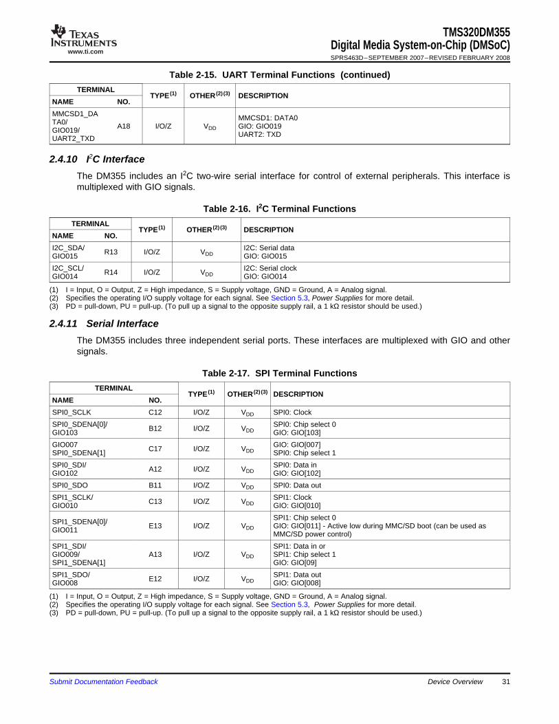
2.4.10 I2C Interface
2.4.11 Serial Interface
TMS320DM355Digital Media System-on-Chip (DMSoC)SPRS463D–SEPTEMBER 2007–REVISED FEBRUARY 2008
Table 2-15. UART Terminal Functions (continued)TERMINAL
TYPE (1) OTHER (2) (3) DESCRIPTIONNAME NO.MMCSD1_DA MMCSD1: DATA0TA0/ A18 I/O/Z VDD GIO: GIO019GIO019/ UART2: TXDUART2_TXD
The DM355 includes an I2C two-wire serial interface for control of external peripherals. This interface ismultiplexed with GIO signals.
Table 2-16. I2C Terminal FunctionsTERMINAL
TYPE (1) OTHER (2) (3) DESCRIPTIONNAME NO.I2C_SDA/ I2C: Serial dataR13 I/O/Z VDDGIO015 GIO: GIO015I2C_SCL/ I2C: Serial clockR14 I/O/Z VDDGIO014 GIO: GIO014
(1) I = Input, O = Output, Z = High impedance, S = Supply voltage, GND = Ground, A = Analog signal.(2) Specifies the operating I/O supply voltage for each signal. See Section 5.3, Power Supplies for more detail.(3) PD = pull-down, PU = pull-up. (To pull up a signal to the opposite supply rail, a 1 kΩ resistor should be used.)
The DM355 includes three independent serial ports. These interfaces are multiplexed with GIO and othersignals.
Table 2-17. SPI Terminal FunctionsTERMINAL
TYPE (1) OTHER (2) (3) DESCRIPTIONNAME NO.SPI0_SCLK C12 I/O/Z VDD SPI0: ClockSPI0_SDENA[0]/ SPI0: Chip select 0B12 I/O/Z VDDGIO103 GIO: GIO[103]GIO007 GIO: GIO[007]C17 I/O/Z VDDSPI0_SDENA[1] SPI0: Chip select 1SPI0_SDI/ SPI0: Data inA12 I/O/Z VDDGIO102 GIO: GIO[102]SPI0_SDO B11 I/O/Z VDD SPI0: Data outSPI1_SCLK/ SPI1: ClockC13 I/O/Z VDDGIO010 GIO: GIO[010]
SPI1: Chip select 0SPI1_SDENA[0]/ E13 I/O/Z VDD GIO: GIO[011] - Active low during MMC/SD boot (can be used asGIO011 MMC/SD power control)SPI1_SDI/ SPI1: Data in orGIO009/ A13 I/O/Z VDD SPI1: Chip select 1SPI1_SDENA[1] GIO: GIO[09]SPI1_SDO/ SPI1: Data outE12 I/O/Z VDDGIO008 GIO: GIO[008]
(1) I = Input, O = Output, Z = High impedance, S = Supply voltage, GND = Ground, A = Analog signal.(2) Specifies the operating I/O supply voltage for each signal. See Section 5.3, Power Supplies for more detail.(3) PD = pull-down, PU = pull-up. (To pull up a signal to the opposite supply rail, a 1 kΩ resistor should be used.)
Submit Documentation Feedback Device Overview 31
www.ti.com
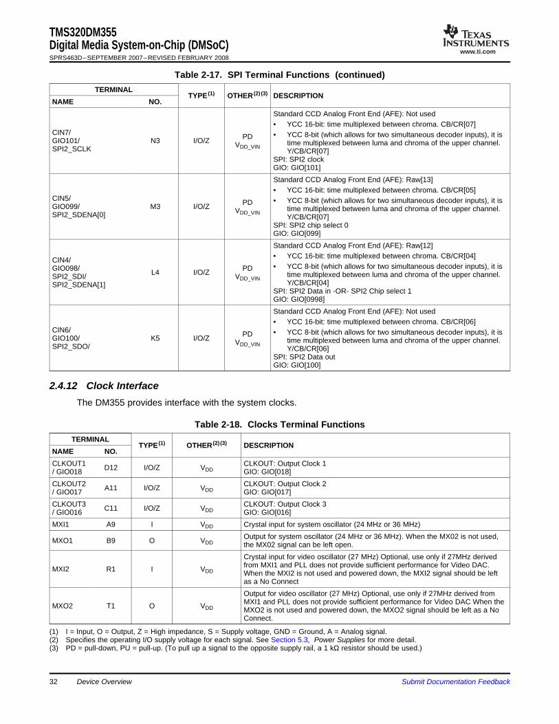
2.4.12 Clock Interface
TMS320DM355Digital Media System-on-Chip (DMSoC)SPRS463D–SEPTEMBER 2007–REVISED FEBRUARY 2008
Table 2-17. SPI Terminal Functions (continued)TERMINAL
TYPE (1) OTHER (2) (3) DESCRIPTIONNAME NO.
Standard CCD Analog Front End (AFE): Not used• YCC 16-bit: time multiplexed between chroma. CB/CR[07]
CIN7/ • YCC 8-bit (which allows for two simultaneous decoder inputs), it isPDGIO101/ N3 I/O/Z time multiplexed between luma and chroma of the upper channel.VDD_VINSPI2_SCLK Y/CB/CR[07]SPI: SPI2 clockGIO: GIO[101]Standard CCD Analog Front End (AFE): Raw[13]• YCC 16-bit: time multiplexed between chroma. CB/CR[05]
CIN5/ • YCC 8-bit (which allows for two simultaneous decoder inputs), it isPDGIO099/ M3 I/O/Z time multiplexed between luma and chroma of the upper channel.VDD_VINSPI2_SDENA[0] Y/CB/CR[07]SPI: SPI2 chip select 0GIO: GIO[099]Standard CCD Analog Front End (AFE): Raw[12]• YCC 16-bit: time multiplexed between chroma. CB/CR[04]CIN4/• YCC 8-bit (which allows for two simultaneous decoder inputs), it isGIO098/ PDL4 I/O/Z time multiplexed between luma and chroma of the upper channel.SPI2_SDI/ VDD_VIN Y/CB/CR[04]SPI2_SDENA[1]SPI: SPI2 Data in -OR- SPI2 Chip select 1GIO: GIO[0998]Standard CCD Analog Front End (AFE): Not used• YCC 16-bit: time multiplexed between chroma. CB/CR[06]
CIN6/ • YCC 8-bit (which allows for two simultaneous decoder inputs), it isPDGIO100/ K5 I/O/Z time multiplexed between luma and chroma of the upper channel.VDD_VINSPI2_SDO/ Y/CB/CR[06]SPI: SPI2 Data outGIO: GIO[100]
The DM355 provides interface with the system clocks.
Table 2-18. Clocks Terminal FunctionsTERMINAL
TYPE (1) OTHER (2) (3) DESCRIPTIONNAME NO.CLKOUT1 CLKOUT: Output Clock 1D12 I/O/Z VDD/ GIO018 GIO: GIO[018]CLKOUT2 CLKOUT: Output Clock 2A11 I/O/Z VDD/ GIO017 GIO: GIO[017]CLKOUT3 CLKOUT: Output Clock 3C11 I/O/Z VDD/ GIO016 GIO: GIO[016]MXI1 A9 I VDD Crystal input for system oscillator (24 MHz or 36 MHz)
Output for system oscillator (24 MHz or 36 MHz). When the MX02 is not used,MXO1 B9 O VDD the MX02 signal can be left open.Crystal input for video oscillator (27 MHz) Optional, use only if 27MHz derivedfrom MXI1 and PLL does not provide sufficient performance for Video DAC.MXI2 R1 I VDD When the MXI2 is not used and powered down, the MXI2 signal should be leftas a No ConnectOutput for video oscillator (27 MHz) Optional, use only if 27MHz derived fromMXI1 and PLL does not provide sufficient performance for Video DAC When theMXO2 T1 O VDD MXO2 is not used and powered down, the MXO2 signal should be left as a NoConnect.
(1) I = Input, O = Output, Z = High impedance, S = Supply voltage, GND = Ground, A = Analog signal.(2) Specifies the operating I/O supply voltage for each signal. See Section 5.3, Power Supplies for more detail.(3) PD = pull-down, PU = pull-up. (To pull up a signal to the opposite supply rail, a 1 kΩ resistor should be used.)
Device Overview32 Submit Documentation Feedback

www.ti.com
2.4.13 Real Time Output (RTO) Interface
2.4.14 Pulse Width Modulator (PWM) Interface
TMS320DM355Digital Media System-on-Chip (DMSoC)SPRS463D–SEPTEMBER 2007–REVISED FEBRUARY 2008
The DM355 provides Real Time Output (RTO) interface.
Table 2-19. RTO Terminal FunctionsTERMINAL
TYPE (1) OTHER (2) (3) DESCRIPTIONNAME NO.COUT5-G2 / Digital Video Out: VENC settings determine function GIO: GIO[079]GIO079 / C1 I/O/Z VDD_VOUT PWM2APWM2A / RTO0RTO0COUT4-B7 / Digital Video Out: VENC settings determine function GIO: GIO[078]GIO078 / D3 I/O/Z VDD_VOUT PWM2BPWM2B / RTO1RTO1COUT3-B6 / Digital Video Out: VENC settings determine function GIO: GIO[077]GIO077 / E3 I/O/Z VDD_VOUT PWM2CPWM2C / RTO2RTO2COUT2-B5 / Digital Video Out: VENC settings determine function GIO: GIO[076]GIO076 / E4 I/O/Z VDD_VOUT PWM2DPWM2D / RTO3RTO3
(1) I = Input, O = Output, Z = High impedance, S = Supply voltage, GND = Ground, A = Analog signal.(2) Specifies the operating I/O supply voltage for each signal. See Section 5.3, Power Supplies for more detail.(3) PD = pull-down, PU = pull-up. (To pull up a signal to the opposite supply rail, a 1 kΩ resistor should be used.)
The DM355 provides Pulse Width Modulator (PWM) interface.
Table 2-20. PWM Terminal FunctionsTERMINAL
TYPE (1) OTHER (2) (3) DESCRIPTIONNAME NO.COUT7-G4 / Digital Video Out: VENC settings determine function GIO: GIO[081]C2 I/O/Z VDD_VOUTGIO081 / PWM0PWM0COUT6-G3 / Digital Video Out: VENC settings determine function GIO: GIO[080]D2 I/O/Z VDD_VOUTGIO080 / PWM1PWM1COUT5-G2 / Digital Video Out: VENC settings determine function GIO: GIO[079]GIO079 / C1 I/O/Z VDD_VOUT PWM2APWM2A / RTO0RTO0COUT4-B7 / Digital Video Out: VENC settings determine function GIO: GIO[078]GIO078 / D3 I/O/Z VDD_VOUT PWM2BPWM2B / RTO1RTO1
(1) I = Input, O = Output, Z = High impedance, S = Supply voltage, GND = Ground, A = Analog signal.(2) Specifies the operating I/O supply voltage for each signal. See Section 5.3, Power Supplies for more detail.(3) PD = pull-down, PU = pull-up. (To pull up a signal to the opposite supply rail, a 1 kΩ resistor should be used.)
Submit Documentation Feedback Device Overview 33

www.ti.com
2.4.15 System Configuration Interface
TMS320DM355Digital Media System-on-Chip (DMSoC)SPRS463D–SEPTEMBER 2007–REVISED FEBRUARY 2008
Table 2-20. PWM Terminal Functions (continued)TERMINAL
TYPE (1) OTHER (2) (3) DESCRIPTIONNAME NO.COUT3-B6 / Digital Video Out: VENC settings determine function GIO: GIO[077]GIO077 / E3 I/O/Z VDD_VOUT PWM2CPWM2C / RTO2RTO2COUT2-B5 / Digital Video Out: VENC settings determine function GIO: GIO[076]GIO076 / E4 I/O/Z VDD_VOUT PWM2DPWM2D / RTO3RTO3COUT1-B4 / Digital Video Out: VENC settings determine function GIO: GIO[075]F3 I/O/Z VDD_VOUTGIO075 / PWM3APWM3ACOUT0-B3 / Digital Video Out: VENC settings determine function GIO: GIO[074]F4 I/O/Z VDD_VOUTGIO074 / PWM3BPWM3BFIELD / Video Encoder: Field identifier for interlaced display formats GIO: GIO[070]GIO070 / H4 I/O/Z VDD_VOUT Digital Video Out: R2R2 / PWM3CPWM3CEXTCLK / Video Encoder: External clock input, used if clock rates > 27 MHz are needed,GIO069 / PDG3 I/O/Z e.g. 74.25 MHz for HDTV digital output GIO: GIO[069] Digital Video Out: B2B2 / VDD_VOUT PWM3DPWM3D
The DM355 provides interfaces for system configuration and boot load.
Table 2-21. System/Boot Terminal FunctionsTERMINAL
TYPE (1) OTHER (2) (3) DESCRIPTIONNAME NO.
Async EMIF: Address bus bit 13EM_A13/ PD GIO: GIO[067]GIO067/ V19 I/O/Z VDD System: BTSEL[1:0] sampled at power-on-reset to determine boot method. UsedBTSEL[1] to drive boot status LED signal (active low) in ROM boot modes.EM_A12/ Async EMIF: Address bus bit 12PDGIO066/ U19 I/O/Z GIO: GIO[066]VDDBTSEL[0] System: BTSEL[1:0] sampled at power-on-reset to determine boot method.
Async EMIF: Address bus bit 11EM_A11/ GIO: GIO[065]PUGIO065/ R16 I/O/Z System: AECFG[3:0] sampled a power-on-reset to set AEMIF configuration.VDDAECFG[3] AECFG[3] sets default fo PinMux2.EM_D15_8. AEMIF default bus width (16 or 8
bits).Async EMIF: Address bus bit 10
EM_A10/ GIO: GIO[064]PUGIO064/ R18 I/O/Z System: AECFG[3:0] sampled a power-on-reset to set AEMIF configuration.VDDAECFG[2] AECFG[2:1] sets default fo PinMux2.EM_BA0. AEMIF EM_BA0 definition:(EM,_BA0, EM_A14, GIO[054], rsvd)Async EMIF: Address bus bit 09
EM_A09/ GIO: GIO[063]PDGIO063/ P17 I/O/Z System: AECFG[3:0] sampled a power-on-reset to set AEMIF configuration.VDDAECFG[1] AECFG[2:1] sets default fo PinMux2.EM_BA0. AEMIF EM_BA0 definition:(EM,_BA0, EM_A14, GIO[054], rsvd)
(1) I = Input, O = Output, Z = High impedance, S = Supply voltage, GND = Ground, A = Analog signal.(2) Specifies the operating I/O supply voltage for each signal. See Section 5.3, Power Supplies for more detail.(3) PD = pull-down, PU = pull-up. (To pull up a signal to the opposite supply rail, a 1 kΩ resistor should be used.)
Device Overview34 Submit Documentation Feedback

www.ti.com
2.4.16 Emulation
TMS320DM355Digital Media System-on-Chip (DMSoC)SPRS463D–SEPTEMBER 2007–REVISED FEBRUARY 2008
Table 2-21. System/Boot Terminal Functions (continued)TERMINAL
TYPE (1) OTHER (2) (3) DESCRIPTIONNAME NO.
Async EMIF: Address bus bit 08GIO: GIO[062]EM_A08/ PD System: AECFG[0] sets default for:GIO062/ T19 I/O/Z VDDAECFG[0] • PinMux2.EM_A0_BA1 - AEMIF address width (OneNAND, or NAND)• PinMux2.EM_A13_3 - AEMIF address width (OneNAND, or NAND)
The emulation interface allow software and hardware debugging.
Table 2-22. Emulation Terminal FunctionsTERMINAL
TYPE (1) OTHER (2) (3) DESCRIPTIONNAME NO.TCK E10 I VDD JTAG test clock input
PUTDI D9 I JTAG test data inputVDD
TDO E9 O VDD JTAG test data outputPUTMS D8 I JTAG test mode selectVDD
PDTRST C9 I JTAG test logic reset (active low)VDD
RTCK E11 O VDD JTAG test clock outputJTAG emulation 0 I/OPUEMU0 E8 I/O/Z EMU[1:0] = 00 - Force Debug Scan chain (ARM and ARM ETB TAPs connected)VDD EMU[1:0] = 11 - Normal Scan chain (ICEpick only)JTAG emulation 1 I/OPUEMU1 E7 I/O/Z EMU[1:0] = 00 - Force Debug Scan chain (ARM and ARM ETB TAPs connected)VDD EMU[1:0] = 11 - Normal Scan chain (ICEpick only)
(1) I = Input, O = Output, Z = High impedance, S = Supply voltage, GND = Ground, A = Analog signal.(2) Specifies the operating I/O supply voltage for each signal. See Section 5.3, Power Supplies for more detail.(3) PD = pull-down, PU = pull-up. (To pull up a signal to the opposite supply rail, a 1 kΩ resistor should be used.)
Submit Documentation Feedback Device Overview 35

www.ti.com
2.5 Pin List
TMS320DM355Digital Media System-on-Chip (DMSoC)SPRS463D–SEPTEMBER 2007–REVISED FEBRUARY 2008
Table 2-23 provides a complete pin description list in pin number order.
Table 2-23. DM355 Pin DescriptionsName BGA Type Group Power PU Reset Description (4) Mux Control
ID (1) Supply (2) PD (3) StateCIN7 / GIO101 / N3 I/O CCDC VDD_VIN PD in Standard CCD Analog Front End (AFE): PINMUX0[1:0].CIN_SPI2_SCLK / GIO / NOT USED 7
SPI2 YCC 16-bit: time multiplexed betweenchroma: CB/CR[07]YCC 08-bit (which allows for 2 simultaneousdecoder inputs), it is time multiplexedbetweenluma and chroma of the upper channel.Y/CB/CR[07]SPI: SPI2 ClockGIO: GIO[101]
CIN6 / GIO100 / K5 I/O CCDC VDD_VIN PD in Standard CCD Analog Front End (AFE): PINMUX0[3:2].CIN_SPI2_SDO / GIO / NOT USED 6
SPI2 YCC 16-bit: time multiplexed betweenchroma: CB/CR[06]YCC 08-bit (which allows for 2 simultaneousdecoder inputs), it is time multiplexedbetween luma and chroma of the upperchannel. Y/CB/CR[06]SPI: SPI2 Data OutGIO: GIO[100]
CIN5 / GIO099 / M3 I/O CCDC VDD_VIN PD in Standard CCD Analog Front End (AFE): PINMUX0[5:4].CIN_SPI2_SDENA[0] / GIO / raw[13] 5
SPI2YCC 16-bit: time multiplexed betweenchroma: CB/CR[05]YCC 08-bit (which allows for 2 simultaneousdecoder inputs), it is time multiplexedbetween luma and chroma of the upperchannel. Y/CB/CR[05]SPI: SPI2 Chip Select 0GIO: GIO[99]
CIN4 / GIO098 / L4 I/O CCDC VDD_VIN PD in Standard CCD Analog Front End (AFE): PINMUX0[7:6].CIN_SPI2_SDI / / GIO / raw[12] 4SPI2_SDENA[1] SPI2 /
SPI2YCC 16-bit: time multiplexed betweenchroma: CB/CR[04]YCC 08-bit (which allows for 2 simultaneousdecoder inputs), it is time multiplexedbetween luma and chroma of the upperchannel. Y/CB/CR[04]SPI: SPI2 Data In -OR- SPI2 Chip select 1GIO: GIO[098]
(1) I = Input, O = Output, Z = High impedance, S = Supply voltage, GND = Ground, A = Analog signal.(2) Specifies the operating I/O supply voltage for each signal. See Section 5.3, Power Supplies for more detail.(3) PD = pull-down, PU = pull-up. (To pull up a signal to the opposite supply rail, a 1 kΩ resistor should be used.)(4) To reduce EMI and reflections, depending on the trace length, approximately 22 Ω to 50 Ω damping resistors are recommend on the
following outputs placed near the DM355: YOUT(0-7),COUT(0-7), HSYNC,VSYNC,LCD_OE,FIELD,EXTCLK,VCLK. The trace lengthsshould be minimized.
Device Overview36 Submit Documentation Feedback

www.ti.com
TMS320DM355Digital Media System-on-Chip (DMSoC)SPRS463D–SEPTEMBER 2007–REVISED FEBRUARY 2008
Table 2-23. DM355 Pin Descriptions (continued)Name BGA Type Group Power PU Reset Description (4) Mux Control
ID (1) Supply (2) PD (3) StateCIN3 / GIO097 J4 I/O CCDC VDD_VIN PD in Standard CCD Analog Front End (AFE): PINMUX0[8].CIN_32
/ GIO raw[11]YCC 16-bit: time multiplexed betweenchroma: CB/CR[03]YCC 08-bit (which allows for 2 simultaneousdecoder inputs), it is time multiplexedbetween luma and chroma of the upperchannel. Y/CB/CR[03]GIO: GIO[097]
CIN2 / GIO096 J5 I/O CCDC VDD_VIN PD in Standard CCD Analog Front End (AFE): PINMUX0[8].CIN_32/ GIO raw[10]
YCC 16-bit: time multiplexed betweenchroma: CB/CR[02]YCC 08-bit (which allows for 2 simultaneousdecoder inputs), it is time multiplexedbetween luma and chroma of the upperchannel. Y/CB/CR[02]GIO: GIO[096]
CIN1 / GIO095 L3 I/O CCDC VDD_VIN PD in Standard CCD Analog Front End (AFE): PINMUX0[9].CIN_10/ GIO raw[09]
YCC 16-bit: time multiplexed betweenchroma: CB/CR[01]YCC 08-bit (which allows for 2 simultaneousdecoder inputs), it is time multiplexedbetween luma and chroma of the upperchannel. Y/CB/CR[01]GIO: GIO[095]
CIN0 / GIO094 J3 I/O CCDC VDD_VIN PD in Standard CCD Analog Front End (AFE): PINMUX0[9].CIN_10/ GIO raw[08]
YCC 16-bit: time multiplexed betweenchroma: CB/CR[00]YCC 08-bit (which allows for 2 simultaneousdecoder inputs), it is time multiplexedbetween luma and chroma of the upperchannel. Y/CB/CR[00]GIO: GIO[094]
YIN7 / GIO093 L5 I/O CCDC VDD_VIN PD in Standard CCD Analog Front End (AFE): PINMUX0[10].YIN_7/ GIO raw[07] 0
YCC 16-bit: time multiplexed between luma:Y[07]YCC 08-bit (which allows for 2 simultaneousdecoder inputs), it is time multiplexedbetween luma and chroma of the lowerchannel. Y/CB/CR[07]GIO: GIO[093]
YIN6 / GIO092 M4 I/O CCDC VDD_VIN PD in Standard CCD Analog Front End (AFE): PINMUX0[10].YIN_7/ GIO raw[06] 0
YCC 16-bit: time multiplexed between luma:Y[06]YCC 08-bit (which allows for 2 simultaneousdecoder inputs), it is time multiplexedbetween luma and chroma of the lowerchannel. Y/CB/CR[06]GIO: GIO[092]
Submit Documentation Feedback Device Overview 37

www.ti.com
TMS320DM355Digital Media System-on-Chip (DMSoC)SPRS463D–SEPTEMBER 2007–REVISED FEBRUARY 2008
Table 2-23. DM355 Pin Descriptions (continued)Name BGA Type Group Power PU Reset Description (4) Mux Control
ID (1) Supply (2) PD (3) StateYIN5 / GIO091 M5 I/O CCDC VDD_VIN PD in Standard CCD Analog Front End (AFE): PINMUX0[10].YIN_7
/ GIO raw[05] 0YCC 16-bit: time multiplexed between luma:Y[05]YCC 08-bit (which allows for 2 simultaneousdecoder inputs), it is time multiplexedbetween luma and chroma of the lowerchannel. Y/CB/CR[05]GIO: GIO[091]
YIN4 / GIO090 P3 I/O CCDC VDD_VIN PD in Standard CCD Analog Front End (AFE): PINMUX0[10].YIN_7/ GIO raw[04] 0
YCC 16-bit: time multiplexed between luma:Y[04]YCC 08-bit (which allows for 2 simultaneousdecoder inputs), it is time multiplexedbetween luma and chroma of the lowerchannel. Y/CB/CR[04]GIO: GIO[090]
YIN3 / GIO089 R3 I/O CCDC VDD_VIN PD in Standard CCD Analog Front End (AFE): PINMUX0[10].YIN_7/ GIO raw[03] 0
YCC 16-bit: time multiplexed between luma:Y[03]YCC 08-bit (which allows for 2 simultaneousdecoder inputs), it is time multiplexedbetween luma and chroma of the lowerchannel. Y/CB/CR[03]GIO: GIO[089]
YIN2 / GIO088 P4 I/O CCDC VDD_VIN PD in Standard CCD Analog Front End (AFE): PINMUX0[10].YIN_7/ GIO raw[02] 0
YCC 16-bit: time multiplexed between luma:Y[02]YCC 08-bit (which allows for 2 simultaneousdecoder inputs), it is time multiplexedbetween luma and chroma of the lowerchannel. Y/CB/CR[02]GIO: GIO[088]
YIN1 / GIO087 P2 I/O CCDC VDD_VIN PD in Standard CCD Analog Front End (AFE): PINMUX0[10].YIN_7/ GIO raw[01] 0
YCC 16-bit: time multiplexed between luma:Y[01]YCC 08-bit (which allows for 2 simultaneousdecoder inputs), it is time multiplexedbetween luma and chroma of the lowerchannel. Y/CB/CR[01]GIO: GIO[087]
YIN0 / GIO086 P5 I/O CCDC VDD_VIN PD in Standard CCD Analog Front End (AFE): PINMUX0[10].YIN_7/ GIO raw[00] 0
YCC 16-bit: time multiplexed between luma:Y[00]YCC 08-bit (which allows for 2 simultaneousdecoder inputs), it is time multiplexedbetween luma and chroma of the lowerchannel. Y/CB/CR[00]GIO: GIO[086]
Device Overview38 Submit Documentation Feedback

www.ti.com
TMS320DM355Digital Media System-on-Chip (DMSoC)SPRS463D–SEPTEMBER 2007–REVISED FEBRUARY 2008
Table 2-23. DM355 Pin Descriptions (continued)Name BGA Type Group Power PU Reset Description (4) Mux Control
ID (1) Supply (2) PD (3) StateCAM_HD / N5 I/O CCDC VDD_VIN PD in Horizontal synchronization signal that can be PINMUX0[11].CAM_GIO085 / GIO either an input (slave mode) or an output HD
(master mode). Tells the CCDC when a newline starts.GIO: GIO[085]
CAM_VD / R4 I/O CCDC VDD_VIN PD in Vertical synchronization signal that can be PINMUX0[12].CAM_GIO084 / GIO either an input (slave mode) or an output VD
(master mode). Tells the CCDC when a newframe starts.GIO: GIO[084]
CAM_WEN_FIE R5 I/O CCDC VDD_VIN PD in Write enable input signal is used by external PINMUX0[13].CAM_LD / GIO083 / GIO device (AFE/TG) to gate the DDR output of WEN
the CCDC module.Alternately, the field identification input plussignal is used by external device (AFE/TG)to indicate the which of two frames is inputto the CCDC module for sensors withinterlaced output. CCDC handles 1- or2-field sensors in hardware.GIO: GIO[083] CCDC.MODE[7].CC
DMD &CCDC.MODE[5].SWEN
PCLK / GIO082 T3 I/O CCDC VDD_VIN PD in Pixel clock input (strobe for lines CI7 through PINMUX0[14].PCLK/ GIO YI0)
GIO: GIO[082]YOUT7-R7 C3 I/O VENC VDD_VOUT in Digital Video Out: VENC settings determine
function (4)
YOUT6-R6 A4 I/O VENC VDD_VOUT in Digital Video Out: VENC settings determinefunction (4)
YOUT5-R5 B4 I/O VENC VDD_VOUT in Digital Video Out: VENC settings determinefunction (4)
YOUT4-R4 B3 I/O VENC VDD_VOUT in Digital Video Out: VENC settings determinefunction (4)
YOUT3-R3 B2 I/O VENC VDD_VOUT in Digital Video Out: VENC settings determinefunction (4)
YOUT2-G7 A3 I/O VENC VDD_VOUT in Digital Video Out: VENC settings determinefunction (4)
YOUT1-G6 A2 I/O VENC VDD_VOUT in Digital Video Out: VENC settings determinefunction (4)
YOUT0-G5 B1 I/O VENC VDD_VOUT in Digital Video Out: VENC settings determinefunction (4)
COUT7-G4 / C2 I/O VENC VDD_VOUT in Digital Video Out: VENC settings determine PINMUX1[1:0].COUGIO081 / PWM0 / GIO / function T_7
PWM0GIO: GIO[081]PWM0
COUT6-G3 / D2 I/O VENC VDD_VOUT in Digital Video Out: VENC settings determine PINMUX1[3:2].COUGIO080 / PWM1 / GIO / function T_6
PWM1GIO: GIO[080]PWM1 (4)
Submit Documentation Feedback Device Overview 39

www.ti.com
TMS320DM355Digital Media System-on-Chip (DMSoC)SPRS463D–SEPTEMBER 2007–REVISED FEBRUARY 2008
Table 2-23. DM355 Pin Descriptions (continued)Name BGA Type Group Power PU Reset Description (4) Mux Control
ID (1) Supply (2) PD (3) StateCOUT5-G2 / C1 I/O VENC VDD_VOUT in Digital Video Out: VENC settings determine PINMUX1[5:4].COUGIO079 / / GIO / function T_5PWM2A / RTO0 PWM2
/ RTOGIO: GIO[079]PWM2ARTO0 (4)
COUT4-B7 / D3 I/O VENC VDD_VOUT in Digital Video Out: VENC settings determine PINMUX1[7:6].COUGIO078 / / GIO / function T_4PWM2B / RTO1 PWM2
/ RTOGIO: GIO[078]PWM2BRTO1 (4)
COUT3-B6 / E3 I/O VENC VDD_VOUT in Digital Video Out: VENC settings determine PINMUX1[9:8].COUGIO077 / / GIO / function T_3PWM2C / RTO2 PWM2
/ RTOGIO: GIO[077]PWM2CRTO2 (4)
COUT2-B5 / E4 I/O VENC VDD_VOUT in Digital Video Out: VENC settings determine PINMUX1[11:10].COGIO076 / / GIO / function UT_2PWM2D / RTO3 PWM2
/ RTOGIO: GIO[076]PWM2DRTO3 (4)
COUT1-B4 / F3 I/O VENC VDD_VOUT in Digital Video Out: VENC settings determine PINMUX1[13:12].COGIO075 / / GIO / function UT_1PWM3A PWM3
GIO: GIO[075]PWM3A (4)
COUT0-B3 / F4 I/O VENC VDD_VOUT in Digital Video Out: VENC settings determine PINMUX1[15:14].COGIO074 / / GIO / function UT_0PWM3B PWM3
GIO: GIO[074]PWM3B (4)
HSYNC / F5 I/O VENC VDD_VOUT PD in Video Encoder: Horizontal Sync PINMUX1[16].HVSYGIO073 / GIO NC
GIO: GIO[073] (4)
VSYNC / G5 I/O VENC VDD_VOUT PD in Video Encoder: Vertical Sync PINMUX1[16].HVSYGIO072 / GIO NC
GIO: GIO[072] (4)
LCD_OE / H5 I/O VENC VDD_VOUT in Video Encoder: LCD Output Enable or PINMUX1[17].DLCDGIO071 / GIO BRIGHT signal
GIO: GIO[071] (4)
Device Overview40 Submit Documentation Feedback

www.ti.com
TMS320DM355Digital Media System-on-Chip (DMSoC)SPRS463D–SEPTEMBER 2007–REVISED FEBRUARY 2008
Table 2-23. DM355 Pin Descriptions (continued)Name BGA Type Group Power PU Reset Description (4) Mux Control
ID (1) Supply (2) PD (3) StateFIELD / GIO070 H4 I/O VENC VDD_VOUT in Video Encoder: Field identifier for interlaced PINMUX1[19:18].FI/ R2 / PWM3C / GIO / display formats ELD
VENC/PWM3
GIO: GIO[070]Digital Video Out: R2PWM3C (4)
EXTCLK / G3 I/O VENC VDD_VOUT PD in Video Encoder: External clock input, used if PINMUX1[21:20].EXGIO069 / B2 / / GIO / clock rates > 27 MHz are needed, e.g. 74.25 TCLKPWM3D VENC MHz for HDTV digital output
/PWM3
GIO: GIO[069]Digital Video Out: B2PWM3D (4)
VCLK / GIO068 H3 I/O VENC VDD_VOUT out L Video Encoder: Video Output Clock PINMUX1[22].VCLK/ GIO
GIO: GIO[068] (4)
VREF J7 A I/O Video Video DAC: Reference voltage outputDAC (0.45V, 0.1uF to GND)
IOUT E1 A I/O Video Video DAC: Pre video buffer DAC outputDAC (1000 ohm to VFB)
IBIAS F2 A I/O Video Video DAC: External resistor (2550 Ohms toDAC GND) connection for current bias
configurationVFB G1 A I/O Video Video DAC: Pre video buffer DAC output
DAC (1000 ohm to IOUT, 1070 ohm to TVOUT)TVOUT F1 A I/O Video VDDA18_DAC Video DAC: Analog Composite NTSC/PAL
DAC output (SeeFigure 5-31 andFigure 5-32 forcircuit connection)
VDDA18V_DAC L7 PWR Video Video DAC: Analog 1.8V powerDAC
VSSA_DAC L8 GND Video Video DAC: Analog 1.8V groundDAC
DDR_CLK W9 I/O DDR VDD_DDR out L DDR Data ClockDDR_CLK W8 I/O DDR VDD_DDR out H DDR Complementary Data ClockDDR_RAS T6 I/O DDR VDD_DDR out H DDR Row Address StrobeDDR_CAS V9 I/O DDR VDD_DDR out H DDR Column Address StrobeDDR_WE W10 I/O DDR VDD_DDR out H DDR Write Enable (active low)DDR_CS T8 I/O DDR VDD_DDR out H DDR Chip Select (active low)DDR_CKE V10 I/O DDR VDD_DDR out L DDR Clock EnableDDR_DQM[1] U15 I/O DDR VDD_DDR out L Data mask outputs: DDR_DQM1: For
DDR_DQ[15:8]DDR_DQM[0] T12 I/O DDR VDD_DDR out L Data mask outputs: DDR_DQM0: For
DDR_DQ[7:0]DDR_DQS[1] V15 I/O DDR VDD_DDR in Data strobe input/outputs for each byte of
the 16 bit data bus used to synchronize thedata transfers. Output to DDR when writingand inputs when reading.DDR_DQS1: For DDR_DQ[15:8]
Submit Documentation Feedback Device Overview 41

www.ti.com
TMS320DM355Digital Media System-on-Chip (DMSoC)SPRS463D–SEPTEMBER 2007–REVISED FEBRUARY 2008
Table 2-23. DM355 Pin Descriptions (continued)Name BGA Type Group Power PU Reset Description (4) Mux Control
ID (1) Supply (2) PD (3) StateDDR_DQS[0] V12 I/O DDR VDD_DDR in Data strobe input/outputs for each byte of
the 16 bit data bus used to synchronize thedata transfers. Output to DDR when writingand inputs when reading.DDR_DQS0: For DDR_DQ[7:0]
DDR_BA[2] V8 I/O DDR VDD_DDR out L Bank select outputs. Two are required for1Gb DDR2 memories.
DDR_BA[1] U7 I/O DDR VDD_DDR out L Bank select outputs. Two are required for1Gb DDR2 memories.
DDR_BA[0] U8 I/O DDR VDD_DDR out L Bank select outputs. Two are required for1Gb DDR2 memories.
DDR_A13 U6 I/O DDR VDD_DDR out L DDR Address Bus bit 13DDR_A12 V7 I/O DDR VDD_DDR out L DDR Address Bus bit 12DDR_A11 W7 I/O DDR VDD_DDR out L DDR Address Bus bit 11DDR_A10 V6 I/O DDR VDD_DDR out L DDR Address Bus bit 10DDR_A09 W6 I/O DDR VDD_DDR out L DDR Address Bus bit 09DDR_A08 W5 I/O DDR VDD_DDR out L DDR Address Bus bit 08DDR_A07 V5 I/O DDR VDD_DDR out L DDR Address Bus bit 07DDR_A06 U5 I/O DDR VDD_DDR out L DDR Address Bus bit 06DDR_A05 W4 I/O DDR VDD_DDR out L DDR Address Bus bit 05DDR_A04 V4 I/O DDR VDD_DDR out L DDR Address Bus bit 04DDR_A03 W3 I/O DDR VDD_DDR out L DDR Address Bus bit 03DDR_A02 W2 I/O DDR VDD_DDR out L DDR Address Bus bit 02DDR_A01 V3 I/O DDR VDD_DDR out L DDR Address Bus bit 01DDR_A00 V2 I/O DDR VDD_DDR out L DDR Address Bus bit 00DDR_DQ15 W17 I/O DDR VDD_DDR in DDR Data Bus bit 15DDR_DQ14 V16 I/O DDR VDD_DDR in DDR Data Bus bit 14DDR_DQ13 W16 I/O DDR VDD_DDR in DDR Data Bus bit 13DDR_DQ12 U16 I/O DDR VDD_DDR in DDR Data Bus bit 12DDR_DQ11 W15 I/O DDR VDD_DDR in DDR Data Bus bit 11DDR_DQ10 W14 I/O DDR VDD_DDR in DDR Data Bus bit 10DDR_DQ09 V14 I/O DDR VDD_DDR in DDR Data Bus bit 09DDR_DQ08 U13 I/O DDR VDD_DDR in DDR Data Bus bit 08DDR_DQ07 W13 I/O DDR VDD_DDR in DDR Data Bus bit 07DDR_DQ06 V13 I/O DDR VDD_DDR in DDR Data Bus bit 06DDR_DQ05 W12 I/O DDR VDD_DDR in DDR Data Bus bit 05DDR_DQ04 U12 I/O DDR VDD_DDR in DDR Data Bus bit 04DDR_DQ03 T11 I/O DDR VDD_DDR in DDR Data Bus bit 03DDR_DQ02 U11 I/O DDR VDD_DDR in DDR Data Bus bit 02DDR_DQ01 W11 I/O DDR VDD_DDR in DDR Data Bus bit 01DDR_DQ00 V11 I/O DDR VDD_DDR in DDR Data Bus bit 00DDR_ W18 I/O DDR VDD_DDR DDR: Loopback signal for external DQSDQGATE0 gating. Route to DDR and back to
DDR_DQGATE1 with same constraints asused for DDR clock and data.
DDR_ V17 I/O DDR VDD_DDR DDR: Loopback signal for external DQSDQGATE1 gating. Route to DDR and back to
DDR_DQGATE0 with same constraints asused for DDR clock and data.
Device Overview42 Submit Documentation Feedback

www.ti.com
TMS320DM355Digital Media System-on-Chip (DMSoC)SPRS463D–SEPTEMBER 2007–REVISED FEBRUARY 2008
Table 2-23. DM355 Pin Descriptions (continued)Name BGA Type Group Power PU Reset Description (4) Mux Control
ID (1) Supply (2) PD (3) StateDDR_VREF U10 PWR DDRI VDD_DDR DDR: Voltage input for the SSTL_18 IO
O buffersVSSA_DLL R11 GND DDRD VDD_DDR DDR: Ground for the DDR DLL
LLVDDA33_DDRDLL R10 PWR DDRD VDD_DDR DDR: Power (3.3 Volts) for the DDR DLL
LLDDR_ZN T9 I/O DDRI VDD_DDR DDR: Reference output for drive strength
O calibration of N and P channel outputs. Tieto ground via 50 ohm resistor @ 0.5%tolerance.
EM_A13 / V19 I/O AEMI VDD PD in L Async EMIF: Address Bus bit[13] PINMUX2[0].EM_A1GIO067 / F / 3_3,BTSEL[1] GIO /
system
GIO: GIO[067] default set byAECFG[0]
System: BTSEL[1:0] sampled atPower-on-Reset to determine Boot method(00:NAND, 01:Flash, 10:MMC/SD, 11:UART)
EM_A12 / U19 I/O AEMI VDD PD in L Async EMIF: Address Bus bit[12] PINMUX2[0].EM_A1GIO066 / F / 3_3,BTSEL[0] GIO /
system
GIO: GIO[066] default set byAECFG[0]
System: BTSEL[1:0] sampled atPower-on-Reset to determine Boot method(00:NAND, 01:Flash, 10:MMC/SD, 11:UART)
EM_A11 / R16 I/O AEMI VDD PU in H Async EMIF: Address Bus bit[11] PINMUX2[0].EM_A1GIO065 / F / 3_3,AECFG[3] GIO /
system
GIO: GIO[065] default set byAECFG[0]
System: AECFG[3:0] sampled atPower-on-Reset to set AEMIF ConfigurationAECFG[3] sets default forPinMux2.EM_D15_8: AEMIF Default BusWidth (0:16 or 1:8 bits)
EM_A10 / R18 I/O AEMI VDD PU in H Async EMIF: Address Bus bit[10] PINMUX2[0].EM_A1GIO064 / F / 3_3,AECFG[2] GIO /
system
GIO: GIO[064] default set byAECFG[0]
System: AECFG[3:0] sampled atPower-on-Reset to set AEMIF ConfigurationAECFG[2:1] sets default forPinMux2.EM_BA0: AEMIF EM_BA0Definition (00: EM_BA0, 01: EM_A14,10:GIO[054], 11:rsvd)
Submit Documentation Feedback Device Overview 43

www.ti.com
TMS320DM355Digital Media System-on-Chip (DMSoC)SPRS463D–SEPTEMBER 2007–REVISED FEBRUARY 2008
Table 2-23. DM355 Pin Descriptions (continued)Name BGA Type Group Power PU Reset Description (4) Mux Control
ID (1) Supply (2) PD (3) StateEM_A09 / P17 I/O AEMI VDD PD in L Async EMIF: Address Bus bit[09] PINMUX2[0].EM_A1GIO063 / F / 3_3,AECFG[1] GIO /
system
GIO: GIO[063] default set byAECFG[0]
System: AECFG[3:0] sampled atPower-on-Reset to set AEMIF ConfigurationAECFG[2:1] sets default forPinMux2.EM_BA0: AEMIF EM_BA0Definition (00: EM_BA0, 01: EM_A14,10:GIO[054], 11:rsvd)
EM_A08 / T19 I/O AEMI VDD PU in H Async EMIF: Address Bus bit[08] PINMUX2[0].EM_A1GIO062 / F / 3_3,AECFG[0] GIO /
system
GIO: GIO[062] default set byAECFG[0]
AECFG[0] sets default for- PinMux2.EM_A0_BA1: AEMIF AddressWidth (OneNAND or NAND)- PinMux2.EM_A13_3: AEMIF AddressWidth (OneNAND or NAND)(0:AEMIF address bits, 1:GIO[67:57])
EM_A07 / P16 I/O AEMI VDD out L Async EMIF: Address Bus bit[07] PINMUX2[0].EM_A1GIO061 F / 3_3,
GIOGIO: GIO[061] - Used by ROM Bootloader to default set byprovide progress status via LED (active low) AECFG[0]
EM_A06 / P18 I/O AEMI VDD out L Async EMIF: Address Bus bit[06] PINMUX2[0].EM_A1GIO060 F / 3_3,
GIOGIO: GIO[060] default set by
AECFG[0]EM_A05 / R19 I/O AEMI VDD out L Async EMIF: Address Bus bit[05] PINMUX2[0].EM_A1GIO059 F / 3_3,
GIOGIO: GIO[059] default set by
AECFG[0]EM_A04 / P15 I/O AEMI VDD out L Async EMIF: Address Bus bit[04] PINMUX2[0].EM_A1GIO058 F / 3_3,
GIOGIO: GIO[058] default set by
AECFG[0]EM_A03 / N18 I/O AEMI VDD out L Async EMIF: Address Bus bit[03] PINMUX2[0].EM_A1GIO057 F / 3_3,
GIOGIO: GIO[057] default set by
AECFG[0]EM_A02 N15 I/O AEMI VDD out L Async EMIF: Address Bus bit[02]
FNAND/SM/xD: CLE - Command LatchEnable output
Device Overview44 Submit Documentation Feedback
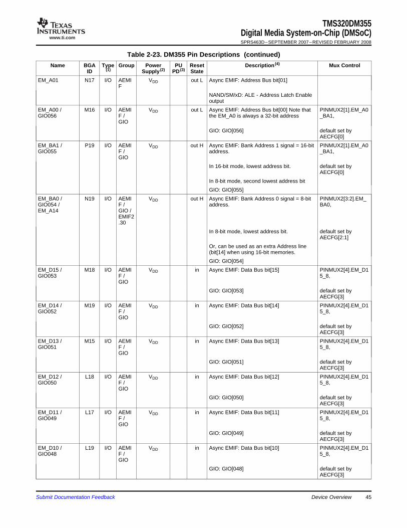
www.ti.com
TMS320DM355Digital Media System-on-Chip (DMSoC)SPRS463D–SEPTEMBER 2007–REVISED FEBRUARY 2008
Table 2-23. DM355 Pin Descriptions (continued)Name BGA Type Group Power PU Reset Description (4) Mux Control
ID (1) Supply (2) PD (3) StateEM_A01 N17 I/O AEMI VDD out L Async EMIF: Address Bus bit[01]
FNAND/SM/xD: ALE - Address Latch Enableoutput
EM_A00 / M16 I/O AEMI VDD out L Async EMIF: Address Bus bit[00] Note that PINMUX2[1].EM_A0GIO056 F / the EM_A0 is always a 32-bit address _BA1,
GIOGIO: GIO[056] default set by
AECFG[0]EM_BA1 / P19 I/O AEMI VDD out H Async EMIF: Bank Address 1 signal = 16-bit PINMUX2[1].EM_A0GIO055 F / address. _BA1,
GIOIn 16-bit mode, lowest address bit. default set by
AECFG[0]In 8-bit mode, second lowest address bitGIO: GIO[055]
EM_BA0 / N19 I/O AEMI VDD out H Async EMIF: Bank Address 0 signal = 8-bit PINMUX2[3:2].EM_GIO054 / F / address. BA0,EM_A14 GIO /
EMIF2.30
In 8-bit mode, lowest address bit. default set byAECFG[2:1]
Or, can be used as an extra Address line(bit[14] when using 16-bit memories.GIO: GIO[054]
EM_D15 / M18 I/O AEMI VDD in Async EMIF: Data Bus bit[15] PINMUX2[4].EM_D1GIO053 F / 5_8,
GIOGIO: GIO[053] default set by
AECFG[3]EM_D14 / M19 I/O AEMI VDD in Async EMIF: Data Bus bit[14] PINMUX2[4].EM_D1GIO052 F / 5_8,
GIOGIO: GIO[052] default set by
AECFG[3]EM_D13 / M15 I/O AEMI VDD in Async EMIF: Data Bus bit[13] PINMUX2[4].EM_D1GIO051 F / 5_8,
GIOGIO: GIO[051] default set by
AECFG[3]EM_D12 / L18 I/O AEMI VDD in Async EMIF: Data Bus bit[12] PINMUX2[4].EM_D1GIO050 F / 5_8,
GIOGIO: GIO[050] default set by
AECFG[3]EM_D11 / L17 I/O AEMI VDD in Async EMIF: Data Bus bit[11] PINMUX2[4].EM_D1GIO049 F / 5_8,
GIOGIO: GIO[049] default set by
AECFG[3]EM_D10 / L19 I/O AEMI VDD in Async EMIF: Data Bus bit[10] PINMUX2[4].EM_D1GIO048 F / 5_8,
GIOGIO: GIO[048] default set by
AECFG[3]
Submit Documentation Feedback Device Overview 45

www.ti.com
TMS320DM355Digital Media System-on-Chip (DMSoC)SPRS463D–SEPTEMBER 2007–REVISED FEBRUARY 2008
Table 2-23. DM355 Pin Descriptions (continued)Name BGA Type Group Power PU Reset Description (4) Mux Control
ID (1) Supply (2) PD (3) StateEM_D09 / K18 I/O AEMI VDD in Async EMIF: Data Bus bit[09] PINMUX2[4].EM_D1GIO047 F / 5_8,
GIOGIO: GIO[047] default set by
AECFG[3]EM_D08 / L16 I/O AEMI VDD in Async EMIF: Data Bus bit[08] PINMUX2[4].EM_D1GIO046 F / 5_8,
GIOGIO: GIO[046] default set by
AECFG[3]EM_D07 / K19 I/O AEMI VDD in Async EMIF: Data Bus bit[07] PINMUX2[5].EM_D7GIO045 F / _0
GIOGIO: GIO[045]
EM_D06 / K17 I/O AEMI VDD in Async EMIF: Data Bus bit[06] PINMUX2[5].EM_D7GIO044 F / _0
GIOGIO: GIO[044]
EM_D05 / J19 I/O AEMI VDD in Async EMIF: Data Bus bit[05] PINMUX2[5].EM_D7GIO043 F / _0
GIOGIO: GIO[043]
EM_D04 / L15 I/O AEMI VDD in Async EMIF: Data Bus bit[04] PINMUX2[5].EM_D7GIO042 F / _0
GIOGIO: GIO[042]
EM_D03 / J18 I/O AEMI VDD in Async EMIF: Data Bus bit[03] PINMUX2[5].EM_D7GIO041 F / _0
GIOGIO: GIO[041]
EM_D02 / H19 I/O AEMI VDD in Async EMIF: Data Bus bit[02] PINMUX2[5].EM_D7GIO040 F / _0
GIOGIO: GIO[040]
EM_D01 / J17 I/O AEMI VDD in Async EMIF: Data Bus bit[01] PINMUX2[5].EM_D7GIO039 F / _0
GIOGIO: GIO[039]
EM_D00 / H18 I/O AEMI VDD in Async EMIF: Data Bus bit[00] PINMUX2[5].EM_D7GIO038 F / _0
GIOGIO: GIO[038]
EM_CE0 / J16 I/O AEMI VDD out H Async EMIF: Lowest numbered Chip Select. PINMUX2[6].EM_CEGIO037 F / Can be programmed to be used for standard 0
GIO asynchronous memories (example:flash),OneNand or NAND memory. Used for thedefault boot and ROM boot modes.GIO: GIO[037]
EM_CE1 / G19 I/O AEMI VDD out H Async EMIF: Second Chip Select., Can be PINMUX2[7].EM_CEGIO036 F / programmed to be used for standard 1
GIO asynchronous memories (example: flash),OneNand or NAND memory.GIO: GIO[036]
Device Overview46 Submit Documentation Feedback
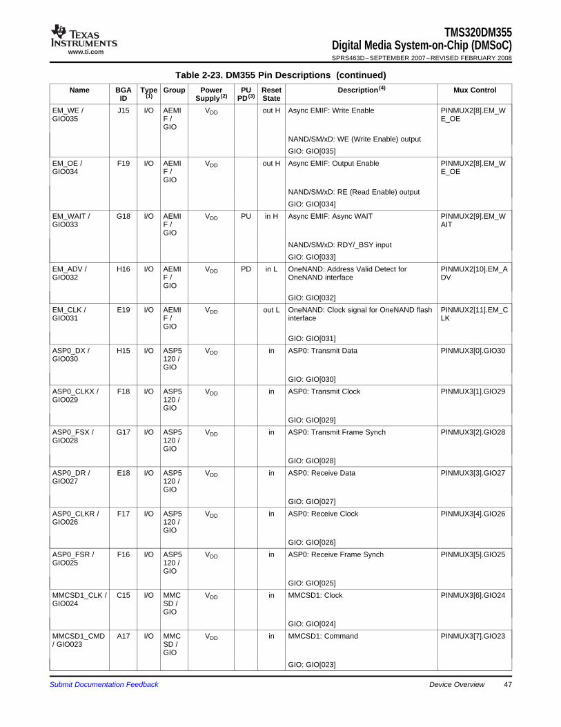
www.ti.com
TMS320DM355Digital Media System-on-Chip (DMSoC)SPRS463D–SEPTEMBER 2007–REVISED FEBRUARY 2008
Table 2-23. DM355 Pin Descriptions (continued)Name BGA Type Group Power PU Reset Description (4) Mux Control
ID (1) Supply (2) PD (3) StateEM_WE / J15 I/O AEMI VDD out H Async EMIF: Write Enable PINMUX2[8].EM_WGIO035 F / E_OE
GIONAND/SM/xD: WE (Write Enable) outputGIO: GIO[035]
EM_OE / F19 I/O AEMI VDD out H Async EMIF: Output Enable PINMUX2[8].EM_WGIO034 F / E_OE
GIONAND/SM/xD: RE (Read Enable) outputGIO: GIO[034]
EM_WAIT / G18 I/O AEMI VDD PU in H Async EMIF: Async WAIT PINMUX2[9].EM_WGIO033 F / AIT
GIONAND/SM/xD: RDY/_BSY inputGIO: GIO[033]
EM_ADV / H16 I/O AEMI VDD PD in L OneNAND: Address Valid Detect for PINMUX2[10].EM_AGIO032 F / OneNAND interface DV
GIOGIO: GIO[032]
EM_CLK / E19 I/O AEMI VDD out L OneNAND: Clock signal for OneNAND flash PINMUX2[11].EM_CGIO031 F / interface LK
GIOGIO: GIO[031]
ASP0_DX / H15 I/O ASP5 VDD in ASP0: Transmit Data PINMUX3[0].GIO30GIO030 120 /
GIOGIO: GIO[030]
ASP0_CLKX / F18 I/O ASP5 VDD in ASP0: Transmit Clock PINMUX3[1].GIO29GIO029 120 /
GIOGIO: GIO[029]
ASP0_FSX / G17 I/O ASP5 VDD in ASP0: Transmit Frame Synch PINMUX3[2].GIO28GIO028 120 /
GIOGIO: GIO[028]
ASP0_DR / E18 I/O ASP5 VDD in ASP0: Receive Data PINMUX3[3].GIO27GIO027 120 /
GIOGIO: GIO[027]
ASP0_CLKR / F17 I/O ASP5 VDD in ASP0: Receive Clock PINMUX3[4].GIO26GIO026 120 /
GIOGIO: GIO[026]
ASP0_FSR / F16 I/O ASP5 VDD in ASP0: Receive Frame Synch PINMUX3[5].GIO25GIO025 120 /
GIOGIO: GIO[025]
MMCSD1_CLK / C15 I/O MMC VDD in MMCSD1: Clock PINMUX3[6].GIO24GIO024 SD /
GIOGIO: GIO[024]
MMCSD1_CMD A17 I/O MMC VDD in MMCSD1: Command PINMUX3[7].GIO23/ GIO023 SD /
GIOGIO: GIO[023]
Submit Documentation Feedback Device Overview 47

www.ti.com
TMS320DM355Digital Media System-on-Chip (DMSoC)SPRS463D–SEPTEMBER 2007–REVISED FEBRUARY 2008
Table 2-23. DM355 Pin Descriptions (continued)Name BGA Type Group Power PU Reset Description (4) Mux Control
ID (1) Supply (2) PD (3) StateMMCSD1_DAT B16 I/O MMC VDD in MMCSD1: DATA3 PINMUX3[9:8].GIO2A3 / GIO022 / SD / 2UART2_RTS GIO /
UART2
GIO: GIO[022]UART2: RTS
MMCSD1_DAT A16 I/O MMC VDD in MMCSD1: DATA2 PINMUX3[11:10].GIA2 / GIO021 / SD / O21UART2_CTS GIO /
UART2
GIO: GIO[021]UART2: CTS
MMCSD1_DAT B15 I/O MMC VDD in MMCSD1: DATA1 PINMUX3[13:12].GIA1 / GIO020 / SD / O20UART2_RXD GIO /
UART2
GIO: GIO[020]UART2: Receive Data
MMCSD1_DAT A18 I/O MMC VDD in MMCSD1: DATA0 PINMUX3[15:14].GIA0 / GIO019 / SD / O19UART2_TXD GIO /
UART2
GIO: GIO[019]UART2: Transmit Data
CLKOUT1 / D12 I/O Clocks VDD in CLKOUT: Output Clock 1 PINMUX3[16].GIO1GIO018 / GIO 8
GIO: GIO[018]CLKOUT2 / A11 I/O Clocks VDD in CLKOUT: Output Clock 2 PINMUX3[17].GIO1GIO017 / GIO 7
GIO: GIO[017]CLKOUT3 / C11 I/O Clocks VDD in CLKOUT: Output Clock 3 PINMUX3[18].GIO1GIO016 / GIO 6
GIO: GIO[016]I2C_SDA / R13 I/O I2C / VDD in I2C: Serial Data PINMUX3[19].GIO1GIO015 GIO 5
GIO: GIO[015]I2C_SCL / R14 I/O I2C / VDD in I2C: Serial Clock PINMUX3[20].GIO1GIO014 GIO 4
GIO: GIO[014]UART1_RXD / R15 I/O UART VDD in UART1: Receive Data PINMUX3[21].GIO1GIO013 1 / 3
GIOGIO: GIO[013]
UART1_TXD / R17 I/O UART VDD in UART1: Transmit Data PINMUX3[22].GIO1GIO012 1 / 2
GIOGIO: GIO[012]
SPI1_SDENA[0] E13 I/O SPI1 / VDD in SPI1: Chip Select 0 PINMUX3[23].GIO1/ GIO011 GIO 1
GIO: GIO[011]
Device Overview48 Submit Documentation Feedback

www.ti.com
TMS320DM355Digital Media System-on-Chip (DMSoC)SPRS463D–SEPTEMBER 2007–REVISED FEBRUARY 2008
Table 2-23. DM355 Pin Descriptions (continued)Name BGA Type Group Power PU Reset Description (4) Mux Control
ID (1) Supply (2) PD (3) StateSPI1_SCLK / C13 I/O SPI1 / VDD in SPI1: Clock PINMUX3[24].GIO1GIO010 GIO 0
GIO: GIO[010]SPI1_SDI / A13 I/O SPI1 / VDD in SPI1: Data In -OR- SPI1: Chip Select 1 PINMUX3[26:25].GIGIO009 / GIO / O9SPI1_SDENA[1] SPI1
GIO: GIO[009]SPI1_SDO / E12 I/O SPI1 / VDD in SPI1: Data Out PINMUX3[27].GIO8GIO008 GIO
GIO: GIO[008]GIO007 / C17 I/O GIO VDD in GIO: GIO[007] PINMUX3[28].GIO7SPI0_SDENA[1] debou
nce /SPI0
SPI0: Chip Select 1GIO006 B18 I/O GIO VDD in GIO: GIO[006]
debounce
GIO005 D15 I/O GIO VDD in GIO: GIO[005]debounce
GIO004 B17 I/O GIO VDD in GIO: GIO[004]debounce
GIO003 G15 I/O GIO VDD in GIO: GIO[003]debounce
GIO002 F15 I/O GIO VDD in GIO: GIO[002]debounce
GIO001 E14 I/O GIO VDD in GIO: GIO[001]debounce
GIO000 C16 I/O GIO VDD in GIO: GIO[000]debounce
USB_DP A7 A I/O USBP VDDA33_USB USB D+ (differential signal pair)HY
USB_DM A6 A I/O USBP VDDA33_USB USB D- (differential signal pair)HY
USB_R1 C7 A I/O USBP USB Reference current outputHY
Connect to VSS_USB_REF via 10K Ω ±1%resistor placed as close to the device aspossible.
USB_ID D5 A I/O USBP VDDA33_USB USB operating mode identification pinHY
For Device mode operation only, pull up thispin to VDD with a 1.5K ohm resistor.For Host mode operation only, pull down thispin to ground (VSS) with a 1.5K ohm resistor.If using an OTG or mini-USB connector, thispin will be set properly via thecable/connector configuration.
Submit Documentation Feedback Device Overview 49
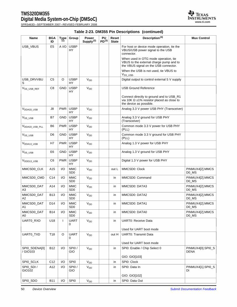
www.ti.com
TMS320DM355Digital Media System-on-Chip (DMSoC)SPRS463D–SEPTEMBER 2007–REVISED FEBRUARY 2008
Table 2-23. DM355 Pin Descriptions (continued)Name BGA Type Group Power PU Reset Description (4) Mux Control
ID (1) Supply (2) PD (3) StateUSB_VBUS E5 A I/O USBP For host or device mode operation, tie the
HY VBUS/USB power signal to the USBconnector.When used in OTG mode operation, tieVBUS to the external charge pump and tothe VBUS signal on the USB connector.When the USB is not used, tie VBUS toVSS_USB.
USB_DRVVBU C5 O USBP VDD Digital output to control external 5 V supplyS HYVSS_USB_REF C8 GND USBP VDD USB Ground Reference
HYConnect directly to ground and to USB_R1via 10K Ω ±1% resistor placed as close tothe device as possible.
VDDA33_USB J8 PWR USBP VDD Analog 3.3 V power USB PHY (Transceiver)HY
VSS_USB B7 GND USBP VDD Analog 3.3 V ground for USB PHYHY (Transceiver)
VDDA33_USB_PLL B6 PWR USBP VDD Common mode 3.3 V power for USB PHYHY (PLL)
VSS_USB D6 GND USBP VDD Common mode 3.3 V ground for USB PHYHY (PLL)
VDDA13_USB H7 PWR USBP VDD Analog 1.3 V power for USB PHYHY
VSS_USB E6 GND USBP VDD Analog 1.3 V ground for USB PHYHY
VDDD13_USB C6 PWR USBP VDD Digital 1.3 V power for USB PHYHY
MMCSD0_CLK A15 I/O MMC VDD out L MMCSD0: Clock PINMUX4[2].MMCSSD0 D0_MS
MMCSD0_CMD C14 I/O MMC VDD in MMCSD0: Command PINMUX4[2].MMCSSD0 D0_MS
MMCSD0_DAT A14 I/O MMC VDD in MMCSD0: DATA3 PINMUX4[2].MMCSA3 SD0 D0_MSMMCSD0_DAT B13 I/O MMC VDD in MMCSD0: DATA2 PINMUX4[2].MMCSA2 SD0 D0_MSMMCSD0_DAT D14 I/O MMC VDD in MMCSD0: DATA1 PINMUX4[2].MMCSA1 SD0 D0_MSMMCSD0_DAT B14 I/O MMC VDD in MMCSD0: DATA0 PINMUX4[2].MMCSA0 SD0 D0_MSUART0_RXD U18 I UART VDD in UART0: Receive Data
0Used for UART boot mode
UART0_TXD T18 O UART VDD out H UART0: Transmit Data0
Used for UART boot modeSPI0_SDENA[0] B12 I/O SPI0 / VDD in SPI0: Enable / Chip Select 0 PINMUX4[0].SPI0_S/ GIO103 GIO DENA
GIO: GIO[103]SPI0_SCLK C12 I/O SPI0 VDD in SPI0: ClockSPI0_SDI / A12 I/O SPI0 / VDD in SPI0: Data In PINMUX4[1].SPI0_SGIO102 GIO DI
GIO: GIO[102]SPI0_SDO B11 I/O SPI0 VDD in SPI0: Data Out
Device Overview50 Submit Documentation Feedback

www.ti.com
TMS320DM355Digital Media System-on-Chip (DMSoC)SPRS463D–SEPTEMBER 2007–REVISED FEBRUARY 2008
Table 2-23. DM355 Pin Descriptions (continued)Name BGA Type Group Power PU Reset Description (4) Mux Control
ID (1) Supply (2) PD (3) StateASP1_DX C18 I/O ASP5 VDD in ASP1: Transmit Data
121ASP1_CLKX D19 I/O ASP5 VDD in ASP1: Transmit Clock
121ASP1_FSX E16 I/O ASP5 VDD in ASP1: Transmit Frame Sync
121ASP1_DR C19 I/O ASP5 VDD in ASP1: Receive Data
121ASP1_CLKR D18 I/O ASP5 VDD in ASP1: Receive Clock
121ASP1_FSR E17 I/O ASP5 VDD in ASP1: Receive Frame Synch
121ASP1_CLKS D17 I ASP5 VDD in ASP1: Master Clock
121RESET D11 I VDD PU in Global Chip Reset (active low)MXI1 A9 I Clocks VDD in Crystal input for system oscillator (24 MHz)MXO1 B9 O Clocks VDD out Output for system oscillator (24 MHz)MXI2 R1 I Clocks VDD in Crystal input for video oscillator (27 MHz).
This crystal is not requiredVDD
MXO2 T1 O Clocks VDD out Output for video oscillator (27 MHz). Thiscrystal is not required.VDD
TCK E10 I EMUL VDD PU in JTAG test clock inputATION
TDI D9 I EMUL VDD PU in JTAG test data inputATION
TDO E9 O EMUL VDD out L JTAG test data outputATION
TMS D8 I EMUL VDD PU in JTAG test mode selectATION
TRST C9 I EMUL VDD PD in JTAG test logic reset (active low)ATION
RTCK E11 O EMUL VDD out L JTAG test clock outputATION
EMU0 E8 I/O EMUL VDD PU in JTAG emulation 0 I/OATIO VDDN
VDD
EMU1 E7 I/O EMUL VDD PU in JTAG emulation 1 I/OATIO EMU[1:0] = 00 - Force Debug Scan chainN (ARM and ARM ETB TAPs connected)
EMU[1:0] = 11 - Normal Scan chain (ICEpickonly)
RSV01 J1 A Reserved. This signal should be left as a NoI/O/Z Connect or connected to VSS.
RSV02 K1 A Reserved. This signal should be left as a NoI/O/Z Connect or connected to VSS.
RSV03 L1 A Reserved. This signal should be left as a NoI/O/Z Connect or connected to VSS.
Submit Documentation Feedback Device Overview 51

www.ti.com
TMS320DM355Digital Media System-on-Chip (DMSoC)SPRS463D–SEPTEMBER 2007–REVISED FEBRUARY 2008
Table 2-23. DM355 Pin Descriptions (continued)Name BGA Type Group Power PU Reset Description (4) Mux Control
ID (1) Supply (2) PD (3) StateRSV04 M1 A Reserved. This signal should be left as a No
I/O/Z Connect or connected to VSS.RSV05 N2 A Reserved. This signal should be connected
I/O/Z to VSS.RSV06 M2 PWR Reserved. This signal should be connected
to VSS.RSV07 K2 GND Reserved. This signal should be connected
to VSS.NC H8 No connectVDD_VIN P6 PWR Power for Digital Video Input IO (3.3 V)VDD_VIN P7 PWR Power for Digital Video Input IO (3.3 V)VDD_VIN P8 PWR Power for Digital Video Input IO (3.3 V)VDD_VOUT F6 PWR Power for Digital Video Output IO (3.3 V)VDD_VOUT F7 PWR Power for Digital Video Output IO (3.3 V)VDD_VOUT F8 PWR Power for Digital Video Output IO (3.3 V)VDD_DDR M9 PWR Power for DDR I/O (1.8 V)VDD_DDR P9 PWR Power for DDR I/O (1.8 V)VDD_DDR P10 PWR Power for DDR I/O (1.8 V)VDD_DDR P11 PWR Power for DDR I/O (1.8 V)VDD_DDR P12 PWR Power for DDR I/O (1.8 V)VDD_DDR P13 PWR Power for DDR I/O (1.8 V)VDD_DDR P14 PWR Power for DDR I/O (1.8 V)VDD_DDR R9 PWR Power for DDR I/O (1.8 V)VDD_DDR R12 PWR Power for DDR I/O (1.8 V)VDD_DDR T14 PWR Power for DDR I/O (1.8 V)VDDA_PLL1 G12 PWR Analog Power for PLL1 (1.3 V)VDDA_PLL2 H9 PWR Analog Power for PLL2 (1.3 V)CVDD A1 PWR Core power (1.3 V)CVDD A10 PWR Core power (1.3 V)CVDD B19 PWR Core power (1.3 V)CVDD C4 PWR Core power (1.3 V)CVDD G6 PWR Core power (1.3 V)CVDD G11 PWR Core power (1.3 V)CVDD H10 PWR Core power (1.3 V)CVDD H13 PWR Core power (1.3 V)CVDD H17 PWR Core power (1.3 V)CVDD J11 PWR Core power (1.3 V)CVDD J12 PWR Core power (1.3 V)CVDD J13 PWR Core power (1.3 V)CVDD K6 PWR Core power (1.3 V)CVDD K11 PWR Core power (1.3 V)CVDD K12 PWR Core power (1.3 V)CVDD L11 PWR Core power (1.3 V)CVDD L12 PWR Core power (1.3 V)CVDD N6 PWR Core power (1.3 V)CVDD R7 PWR Core power (1.3 V)CVDD R8 PWR Core power (1.3 V)CVDD T17 PWR Core power (1.3 V)
Device Overview52 Submit Documentation Feedback

www.ti.com
TMS320DM355Digital Media System-on-Chip (DMSoC)SPRS463D–SEPTEMBER 2007–REVISED FEBRUARY 2008
Table 2-23. DM355 Pin Descriptions (continued)Name BGA Type Group Power PU Reset Description (4) Mux Control
ID (1) Supply (2) PD (3) StateCVDD W19 PWR Core power (1.3 V)VDD F9 PWR Power for Digital IO (3.3 V)VDD F10 PWR Power for Digital IO (3.3 V)VDD F11 PWR Power for Digital IO (3.3 V)VDD F12 PWR Power for Digital IO (3.3 V)VDD F13 PWR Power for Digital IO (3.3 V)VDD F14 PWR Power for Digital IO (3.3 V)VDD G8 PWR Power for Digital IO (3.3 V)VDD G14 PWR Power for Digital IO (3.3 V)VDD K8 PWR Power for Digital IO (3.3 V)VDD K15 PWR Power for Digital IO (3.3 V)VDD L6 PWR Power for Digital IO (3.3 V)VDD L13 PWR Power for Digital IO (3.3 V)VDD M10 PWR Power for Digital IO (3.3 V)VDD M11 PWR Power for Digital IO (3.3 V)VDD M12 PWR Power for Digital IO (3.3 V)VDD M13 PWR Power for Digital IO (3.3 V)VDD N11 PWR Power for Digital IO (3.3 V)VDD N12 PWR Power for Digital IO (3.3 V)VSS_MX1 C10 GND System oscillator (24 MHz) - groundVSS_MX2 P1 GND Video oscillator (27 MHz) - groundVSSA_PLL1 H12 GND Analog Ground for PLL1VSSA_PLL2 J9 GND Analog Ground for PLL2VSS A5 GND Digital groundVSS A8 GND Digital groundVSS A19 GND Digital groundVSS B5 GND Digital groundVSS B8 GND Digital groundVSS B10 GND Digital groundVSS D1 GND Digital groundVSS E2 GND Digital groundVSS E15 GND Digital groundVSS G2 GND Digital groundVSS G9 GND Digital groundVSS H1 GND Digital groundVSS H2 GND Digital groundVSS H6 GND Digital groundVSS H11 GND Digital groundVSS H14 GND Digital groundVSS J2 GND Digital groundVSS J6 GND Digital groundVSS J10 GND Digital groundVSS J14 GND Digital groundVSS K3 GND Digital groundVSS K9 GND Digital groundVSS K10 GND Digital ground
Submit Documentation Feedback Device Overview 53

www.ti.com
TMS320DM355Digital Media System-on-Chip (DMSoC)SPRS463D–SEPTEMBER 2007–REVISED FEBRUARY 2008
Table 2-23. DM355 Pin Descriptions (continued)Name BGA Type Group Power PU Reset Description (4) Mux Control
ID (1) Supply (2) PD (3) StateVSS K14 GND Digital groundVSS L2 GND Digital groundVSS L9 GND Digital groundVSS L10 GND Digital groundVSS L14 GND Digital groundVSS M6 GND Digital groundVSS M7 GND Digital groundVSS M8 GND Digital groundVSS M14 GND Digital groundVSS M17 GND Digital groundVSS N1 GND Digital groundVSS N8 GND Digital groundVSS N9 GND Digital groundVSS N14 GND Digital groundVSS R2 GND Digital groundVSS R6 GND Digital groundVSS T2 GND Digital groundVSS T5 GND Digital groundVSS T15 GND Digital groundVSS U1 GND Digital groundVSS U2 GND Digital groundVSS U3 GND Digital groundVSS U4 GND Digital groundVSS U9 GND Digital groundVSS U14 GND Digital groundVSS U17 GND Digital groundVSS V1 GND Digital groundVSS V18 GND Digital groundVSS W1 GND Digital ground
Device Overview54 Submit Documentation Feedback

www.ti.com
2.6 Device Support
2.6.1 Development Tools
2.6.2 Device Nomenclature
TMS320DM355Digital Media System-on-Chip (DMSoC)SPRS463D–SEPTEMBER 2007–REVISED FEBRUARY 2008
TI offers an extensive line of development tools for DM355 systems, including tools to evaluate theperformance of the processors, generate code, develop algorithm implementations, and fully integrate anddebug software and hardware modules. The tools support documentation is electronically available withinthe Code Composer Studio™ Integrated Development Environment (IDE).
The following products support development of DM355 based applications:
Software Development Tools:Code Composer Studio™ Integrated Development Environment (IDE): including EditorC/C++/Assembly Code Generation, and Debug plus additional development tools
Hardware Development Tools:Extended Development System (XDS™) Emulator (supports TMS320DM355 DMSoC multiprocessorsystem debug) EVM (Evaluation Module)For a complete listing of development-support tools for the TMS320DM355 DMSoC platform, visit theTexas Instruments web site on the Worldwide Web at http://www.ti.com. For information on pricing andavailability, contact the nearest TI field sales office or authorized distributor.
To designate the stages in the product development cycle, TI assigns prefixes to the part numbers of allDSP devices and support tools. Each DSP commercial family member has one of three prefixes: TMX,TMP, or TMS (e.g., ). Texas Instruments recommends two of three possible prefix designators for itssupport tools: TMDX and TMDS. These prefixes represent evolutionary stages of product developmentfrom engineering prototypes (TMX/TMDX) through fully qualified production devices/tools (TMS/TMDS).
Device development evolutionary flow:
TMX Experimental device that is not necessarily representative of the final device's electricalspecifications.
TMP Final silicon die that conforms to the device's electrical specifications but has not completedquality and reliability verification.
TMS Fully-qualified production device.
Support tool development evolutionary flow:
TMDX Development-support product that has not yet completed Texas Instruments internalqualification testing.
TMDS Fully qualified development-support product.
TMX and TMP devices and TMDX development-support tools are shipped against the followingdisclaimer:
"Developmental product is intended for internal evaluation purposes."
TMS devices and TMDS development-support tools have been characterized fully, and the quality andreliability of the device have been demonstrated fully. TI's standard warranty applies.
Predictions show that prototype devices (TMX or TMP) have a greater failure rate than the standardproduction devices. Texas Instruments recommends that these devices not be used in any productionsystem because their expected end-use failure rate is undefined. Only qualified production devices are tobe used in production.
Submit Documentation Feedback Device Overview 55
www.ti.com
DM355
PREFIX
TMX 320 DM355 ZCE
TMX = Experimental deviceTMS = Qualified device
DEVICE FAMILY320 = TMS320 DSP family
PACKAGE TYPE (A)
ZCE = 337-pin plastic BGA, with Pb-free soldered balls
DEVICE(B)
A. BGA = Ball Grid Array
B.
( )
SILICON REVISION
Blank = Initial Silicon1.1
SPEED GRADE216 MHz270 MHz
216
2.6.3 Device Documentation
2.6.3.1 Related Documentation From Texas Instruments
TMS320DM355Digital Media System-on-Chip (DMSoC)SPRS463D–SEPTEMBER 2007–REVISED FEBRUARY 2008
TI device nomenclature also includes a suffix with the device family name. This suffix indicates thepackage type (for example, ZCE), the temperature range (for example, "Blank" is the commercialtemperature range), and the device speed range in megahertz (for example, 202 is 202.5 MHz). Thefollowing figure provides a legend for reading the complete device name for any TMS320DM355 DMSoCplatform member.
Figure 2-5. Device Nomenclature
The following documents describe the TMS320DM35x Digital Media System-on-Chip (DMSoC). Copies ofthese documents are available on the internet at www.ti.com.
SPRS463 TMS320DM355 Digital Media System-on-Chip (DMSoC) Data Manual This documentdescribes the overall TMS320DM355 system, including device architecture and features,memory map, pin descriptions, timing characteristics and requirements, device mechanicals,etc.
SPRZ264 TMS320DM355 DMSoC Silicon Errata Describes the known exceptions to the functionalspecifications for the TMS320DM355 DMSoC.
SPRUFB3 TMS320DM35x Digital Media System-on-Chip (DMSoC) ARM Subsystem ReferenceGuide This document describes the ARM Subsystem in the TMS320DM35x Digital MediaSystem-on-Chip (DMSoC). The ARM subsystem is designed to give the ARM926EJ-S(ARM9) master control of the device. In general, the ARM is responsible for configurationand control of the device; including the components of the ARM Subsystem, the peripherals,and the external memories.
SPRUED1 TMS320DM35x Digital Media System-on-Chip (DMSoC) Asynchronous ExternalMemory Interface (EMIF) Reference Guide This document describes the asynchronousexternal memory interface (EMIF) in the TMS320DM35x Digital Media System-on-Chip(DMSoC). The EMIF supports a glueless interface to a variety of external devices.
SPRUED2 TMS320DM35x Digital Media System-on-Chip (DMSoC) Universal Serial Bus (USB)Controller Reference Guide This document describes the universal serial bus (USB)controller in the TMS320DM35x Digital Media System-on-Chip (DMSoC). The USB controllersupports data throughput rates up to 480 Mbps. It provides a mechanism for data transferbetween USB devices and also supports host negotiation.
SPRUED3 TMS320DM35x Digital Media System-on-Chip (DMSoC) Audio Serial Port (ASP)Reference Guide This document describes the operation of the audio serial port (ASP)
Device Overview56 Submit Documentation Feedback

www.ti.com
TMS320DM355Digital Media System-on-Chip (DMSoC)SPRS463D–SEPTEMBER 2007–REVISED FEBRUARY 2008
audio interface in the TMS320DM35x Digital Media System-on-Chip (DMSoC). The primaryaudio modes that are supported by the ASP are the AC97 and IIS modes. In addition to theprimary audio modes, the ASP supports general serial port receive and transmit operation,but is not intended to be used as a high-speed interface.
SPRUED4 TMS320DM35x Digital Media System-on-Chip (DMSoC) Serial Peripheral Interface (SPI)Reference Guide This document describes the serial peripheral interface (SPI) in theTMS320DM35x Digital Media System-on-Chip (DMSoC). The SPI is a high-speedsynchronous serial input/output port that allows a serial bit stream of programmed length (1to 16 bits) to be shifted into and out of the device at a programmed bit-transfer rate. The SPIis normally used for communication between the DMSoC and external peripherals. Typicalapplications include an interface to external I/O or peripheral expansion via devices such asshift registers, display drivers, SPI EPROMs and analog-to-digital converters.
SPRUED9 TMS320DM35x Digital Media System-on-Chip (DMSoC) Universal AsynchronousReceiver/Transmitter (UART) Reference Guide This document describes the universalasynchronous receiver/transmitter (UART) peripheral in the TMS320DM35x Digital MediaSystem-on-Chip (DMSoC). The UART peripheral performs serial-to-parallel conversion ondata received from a peripheral device, and parallel-to-serial conversion on data receivedfrom the CPU.
SPRUEE0 TMS320DM35x Digital Media System-on-Chip (DMSoC) Inter-Integrated Circuit (I2C)Peripheral Reference Guide This document describes the inter-integrated circuit (I2C)peripheral in the TMS320DM35x Digital Media System-on-Chip (DMSoC). The I2C peripheralprovides an interface between the DMSoC and other devices compliant with the I2C-busspecification and connected by way of an I2C-bus. External components attached to this2-wire serial bus can transmit and receive up to 8-bit wide data to and from the DMSoCthrough the I2C peripheral. This document assumes the reader is familiar with the I2C-busspecification.
SPRUEE2 TMS320DM35x Digital Media System-on-Chip (DMSoC) Multimedia Card (MMC)/SecureDigital (SD) Card Controller Reference Guide This document describes the multimediacard (MMC)/secure digital (SD) card controller in the TMS320DM35x Digital MediaSystem-on-Chip (DMSoC). The MMC/SD card is used in a number of applications to provideremovable data storage. The MMC/SD controller provides an interface to external MMC andSD cards. The communication between the MMC/SD controller and MMC/SD card(s) isperformed by the MMC/SD protocol.
SPRUEE4 TMS320DM35x Digital Media System-on-Chip (DMSoC) Enhanced Direct MemoryAccess (EDMA) Controller Reference Guide This document describes the operation of theenhanced direct memory access (EDMA3) controller in the TMS320DM35x Digital MediaSystem-on-Chip (DMSoC). The EDMA controller's primary purpose is to serviceuser-programmed data transfers between two memory-mapped slave endpoints on theDMSoC.
SPRUEE5 TMS320DM35x Digital Media System-on-Chip (DMSoC) 64-bit Timer Reference GuideThis document describes the operation of the software-programmable 64-bit timers in theTMS320DM35x Digital Media System-on-Chip (DMSoC). Timer 0, Timer 1, and Timer 3 areused as general-purpose (GP) timers and can be programmed in 64-bit mode, dual 32-bitunchained mode, or dual 32-bit chained mode; Timer 2 is used only as a watchdog timer.The GP timer modes can be used to generate periodic interrupts or enhanced direct memoryaccess (EDMA) synchronization events and Real Time Output (RTO) events (Timer 3 only).The watchdog timer mode is used to provide a recovery mechanism for the device in theevent of a fault condition, such as a non-exiting code loop.
SPRUEE6 TMS320DM35x Digital Media System-on-Chip (DMSoC) General-Purpose Input/Output(GPIO) Reference Guide This document describes the general-purpose input/output (GPIO)peripheral in the TMS320DM35x Digital Media System-on-Chip (DMSoC). The GPIO
Submit Documentation Feedback Device Overview 57

www.ti.com
TMS320DM355Digital Media System-on-Chip (DMSoC)SPRS463D–SEPTEMBER 2007–REVISED FEBRUARY 2008
peripheral provides dedicated general-purpose pins that can be configured as either inputsor outputs. When configured as an input, you can detect the state of the input by reading thestate of an internal register. When configured as an output, you can write to an internalregister to control the state driven on the output pin.
SPRUEE7 TMS320DM35x Digital Media System-on-Chip (DMSoC) Pulse-Width Modulator (PWM)Reference Guide This document describes the pulse-width modulator (PWM) peripheral inthe TMS320DM35x Digital Media System-on-Chip (DMSoC).
SPRUEH7 TMS320DM35x Digital Media System-on-Chip (DMSoC) DDR2/Mobile DDR(DDR2/mDDR) Memory Controller Reference Guide This document describes theDDR2/mDDR memory controller in the TMS320DM35x Digital Media System-on-Chip(DMSoC). The DDR2/mDDR memory controller is used to interface with JESD79D-2Astandard compliant DDR2 SDRAM and mobile DDR devices.
SPRUF71 TMS320DM35x Digital Media System-on-Chip (DMSoC) Video Processing Front End(VPFE) Reference Guide This document describes the Video Processing Front End (VPFE)in the TMS320DM35x Digital Media System-on-Chip (DMSoC).
SPRUF72 TMS320DM35x Digital Media System-on-Chip (DMSoC) Video Processing Back End(VPBE) Reference Guide This document describes the Video Processing Back End (VPBE)in the TMS320DM35x Digital Media System-on-Chip (DMSoC).
SPRUF74 TMS320DM35x Digital Media System-on-Chip (DMSoC) Real-Time Out (RTO) ControllerReference Guide This document describes the Real Time Out (RTO) controller in theTMS320DM35x Digital Media System-on-Chip (DMSoC).
SPRUFC8 TMS320DM35x Digital Media System-on-Chip (DMSoC) Peripherals OverviewReference Guide This document provides an overview of the peripherals in theTMS320DM35x Digital Media System-on-Chip (DMSoC).
SPRAAR3 Implementing DDR2/mDDR PCB Layout on the TMS320DM35x DMSoC This providesboard design recommendations and guidelines for DDR2 and mobile DDR.
SPRAAR7 USB 2.0 Board Design and Layout Guidelines This provides board designrecommendations and guidelines for high speed USB.
58 Device Overview Submit Documentation Feedback

www.ti.com
3 Detailed Device Description
3.1 ARM Subsystem Overview
3.1.1 Components of the ARM Subsystem
TMS320DM355Digital Media System-on-Chip (DMSoC)SPRS463D–SEPTEMBER 2007–REVISED FEBRUARY 2008
This section provides a detailed overview of the DM355 device.
The ARM Subsystem contains components required to provide the ARM926EJ-S (ARM) master control ofthe overall DM355 system, including the components of the ARM Subsystem, the peripherals, and theexternal memories.
The ARM is responsible for handling system functions such as system-level initialization, configuration,user interface, user command execution, connectivity functions, interface and control of the subsystem,etc. The ARM is master and performs these functions because it has a large program memory space andfast context switching capability, and is thus suitable for complex, multi-tasking, and general-purposecontrol tasks.
The ARM Subsystem in DM355 consists of the following components:• ARM926EJ-S RISC processor, including:
– coprocessor 15 (CP15)– MMU– 16KB Instruction cache– 8KB Data cache– Write Buffer– Java accelerator
• ARM Internal Memories– 32KB Internal RAM (32-bit wide access)– 8KB Internal ROM (ARM bootloader for non-AEMIF boot options)
• Embedded Trace Module and Embedded Trace Buffer (ETM/ETB)• System Control Peripherals
– ARM Interrupt Controller– PLL Controller– Power and Sleep Controller– System Control Module
The ARM also manages/controls all the device peripherals:• DDR2 / mDDR EMIF Controller• AEMIF Controller, including the OneNAND and NAND flash interface• Enhanced DMA (EDMA)• UART• Timers• Real Time Out (RTO)• Pulse Width Modulator (PWM)• Inter-IC Communication (I2C)• Multi-Media Card/Secure Digital (MMC/SD)• Audio Serial Port (ASP)• Universal Serial Bus Controller (USB)• Serial Port Interface (SPI)• Video Processing Front End (VPFE)
– CCD Controller (CCDC)
Submit Documentation Feedback Detailed Device Description 59

www.ti.com
ARM926EJ-S
16K I$
8K D$ MMU
CP15
Arbiter Arbiter
I-AHB
D-AHB
Master
IF
DM
AB
us
I-TCM
D-TCM
16K
RAM0RAM1
16K
ROM
8K
ArbiterSlave
IF
Master IF
CF
G B
us
ARM
Interrupt
Controller
(AINTC)
Control
System
PLLC2
PLLC1
(PSC)
Controller
Sleep
Power
Peripherals...
3.2 ARM926EJ-S RISC CPU
TMS320DM355Digital Media System-on-Chip (DMSoC)SPRS463D–SEPTEMBER 2007–REVISED FEBRUARY 2008
– Image Pipe (IPIPE)– H3A Engine (Hardware engine for computing Auto-focus, Auto white balance, and Auto exposure)
• Video Processing Back End (VPBE)– On Screen Display (OSD)– Video Encoder Engine (VENC)
Figure 3-1 shows the functional block diagram of the DM355 ARM Subsystem.
Figure 3-1. DM355 ARM Subsystem Block Diagram
The ARM Subsystem integrates the ARM926EJ-S processor. The ARM926EJ-S processor is a member ofARM9 family of general-purpose microprocessors. This processor is targeted at multi-tasking applicationswhere full memory management, high performance, low die size, and low power are all important. TheARM926EJ-S processor supports the 32-bit ARM and 16 bit THUMB instruction sets, enabling the user totrade off between high performance and high code density. Specifically, the ARM926EJ-S processorsupports the ARMv5TEJ instruction set, which includes features for efficient execution of Java byte codes,providing Java performance similar to Just in Time (JIT) Java interpreter, but without associated codeoverhead.
The ARM926EJ-S processor supports the ARM debug architecture and includes logic to assist in bothhardware and software debug. The ARM926EJ-S processor has a Harvard architecture and provides acomplete high performance subsystem, including:• ARM926EJ -S integer core• CP15 system control coprocessor• Memory Management Unit (MMU)• Separate instruction and data Caches• Write buffer• Separate instruction and data Tightly-Coupled Memories (TCMs) [internal RAM] interfaces• Separate instruction and data AHB bus interfaces
Detailed Device Description60 Submit Documentation Feedback

www.ti.com
3.2.1 CP15
3.2.2 MMU
3.2.3 Caches and Write Buffer
TMS320DM355Digital Media System-on-Chip (DMSoC)SPRS463D–SEPTEMBER 2007–REVISED FEBRUARY 2008
• Embedded Trace Module and Embedded Trace Buffer (ETM/ETB)
For more complete details on the ARM9, refer to the ARM926EJ-S Technical Reference Manual, availableat http://www.arm.com
The ARM926EJ-S system control coprocessor (CP15) is used to configure and control instruction anddata caches, Tightly-Coupled Memories (TCMs), Memory Management Unit (MMU), and other ARMsubsystem functions. The CP15 registers are programmed using the MRC and MCR ARM instructions,when the ARM in a privileged mode such as supervisor or system mode.
The ARM926EJ-S MMU provides virtual memory features required by operating systems such as Linux,WindowCE, ultron, ThreadX, etc. A single set of two level page tables stored in main memory is used tocontrol the address translation, permission checks and memory region attributes for both data andinstruction accesses. The MMU uses a single unified Translation Lookaside Buffer (TLB) to cache theinformation held in the page tables. The MMU features are:• Standard ARM architecture v4 and v5 MMU mapping sizes, domains and access protection scheme.• Mapping sizes are:
– 1MB (sections)– 64KB (large pages)– 4KB (small pages)– 1KB (tiny pages)
• Access permissions for large pages and small pages can be specified separately for each quarter ofthe page (subpage permissions)
• Hardware page table walks• Invalidate entire TLB, using CP15 register 8• Invalidate TLB entry, selected by MVA, using CP15 register 8• Lockdown of TLB entries, using CP15 register 10
The size of the Instruction Cache is 16KB, Data cache is 8KB. Additionally, the Caches have the followingfeatures:• Virtual index, virtual tag, and addressed using the Modified Virtual Address (MVA)• Four-way set associative, with a cache line length of eight words per line (32-bytes per line) and with
two dirty bits in the Dcache• Dcache supports write-through and write-back (or copy back) cache operation, selected by memory
region using the C and B bits in the MMU translation tables.• Critical-word first cache refilling• Cache lockdown registers enable control over which cache ways are used for allocation on a line fill,
providing a mechanism for both lockdown, and controlling cache corruption• Dcache stores the Physical Address TAG (PA TAG) corresponding to each Dcache entry in the TAG
RAM for use during the cache line write-backs, in addition to the Virtual Address TAG stored in theTAG RAM. This means that the MMU is not involved in Dcache write-back operations, removing thepossibility of TLB misses related to the write-back address.
• Cache maintenance operations provide efficient invalidation of, the entire Dcache or Icache, regions ofthe Dcache or Icache, and regions of virtual memory.
Submit Documentation Feedback Detailed Device Description 61

www.ti.com
3.2.4 Tightly Coupled Memory (TCM)
3.2.5 Advanced High-performance Bus (AHB)
3.2.6 Embedded Trace Macrocell (ETM) and Embedded Trace Buffer (ETB)
3.3 Memory Mapping
3.3.1 ARM Internal Memories
3.3.2 External Memories
TMS320DM355Digital Media System-on-Chip (DMSoC)SPRS463D–SEPTEMBER 2007–REVISED FEBRUARY 2008
The write buffer is used for all writes to a noncachable bufferable region, write-through region and writemisses to a write-back region. A separate buffer is incorporated in the Dcache for holding write-back forcache line evictions or cleaning of dirty cache lines. The main write buffer has 16-word data buffer and afour-address buffer. The Dcache write-back has eight data word entries and a single address entry.
ARM internal RAM is provided for storing real-time and performance-critical code/data and the InterruptVector table. ARM internal ROM boot options include—NAND, UART, and MMC/SD. The RAM and ROMmemories interfaced to the ARM926EJ-S via the tightly coupled memory interface that provides forseparate instruction and data bus connections. Since the ARM TCM does not allow instructions on theD-TCM bus or data on the I-TCM bus, an arbiter is included so that both data and instructions can bestored in the internal RAM/ROM. The arbiter also allows accesses to the RAM/ROM from extra-ARMsources (e.g., EDMA or other masters). The ARM926EJ-S has built-in DMA support for direct accesses tothe ARM internal memory from a non-ARM master. Because of the time-critical nature of the TCM link tothe ARM internal memory, all accesses from non-ARM devices are treated as DMA transfers.
Instruction and Data accesses are differentiated via accessing different memory map regions, with theinstruction region from 0x0000 through 0x7FFF and data from 0x10000 through 0x17FFF. Placing theinstruction region at 0x0000 is necessary to allow the ARM Interrupt Vector table to be placed at 0x0000,as required by the ARM architecture. The internal 32-KB RAM is split into two physical banks of 16KBeach, which allows simultaneous instruction and data accesses to be accomplished if the code and dataare in separate banks.
The ARM Subsystem uses the AHB port of the ARM926EJ-S to connect the ARM to the configuration busand the external memories. Arbiters are employed to arbitrate access to the separate D-AHB and I-AHBby the configuration bus and the external memories bus.
To support real-time trace, the ARM926EJ-S processor provides an interface to enable connection of anEmbedded Trace Macrocell (ETM). The ARM926ES-J Subsystem in DM355 also includes the EmbeddedTrace Buffer (ETB). The ETM consists of two parts:• Trace Port provides real-time trace capability for the ARM9.• Triggering facilities provide trigger resources, which include address and data comparators, counter,
and sequencers.
The DM355 trace port is not pinned out and is instead only connected to the Embedded Trace Buffer. TheETB has a 4KB buffer memory. ETB enabled debug tools are required to read/interpret the captured tracedata.
The ARM memory map is shown in Table 2-2 and Table 2-3. This section describes the memories andinterfaces within the ARM's memory map.
The ARM has access to the following ARM internal memories:• 32KB ARM Internal RAM on TCM interface, logically separated into two 16KB pages to allow
simultaneous access on any given cycle if there are separate accesses for code (I-TCM bus) and data(D-TCM) to the different memory regions.
• 8KB ARM Internal ROM
The ARM has access to the following External memories:
Detailed Device Description62 Submit Documentation Feedback

www.ti.com
3.3.3 Peripherals
3.4 ARM Interrupt Controller (AINTC)
3.4.1 Interrupt Mapping
TMS320DM355Digital Media System-on-Chip (DMSoC)SPRS463D–SEPTEMBER 2007–REVISED FEBRUARY 2008
• DDR2 / mDDR Synchronous DRAM• Asynchronous EMIF / OneNAND• NAND Flash• Flash card devices:
– MMC/SD– xD– SmartMedia
The ARM has access to all of the peripherals on the DM355 device.
The DM355 ARM Interrupt Controller (AINTC) has the following features:• Supports up to 64 interrupt channels (16 external channels)• Interrupt mask for each channel• Each interrupt channel can be mapped to a Fast Interrupt Request (FIQ) or to an Interrupt Request
(IRQ) type of interrupt.• Hardware prioritization of simultaneous interrupts• Configurable interrupt priority (2 levels of FIQ and 6 levels of IRQ)• Configurable interrupt entry table (FIQ and IRQ priority table entry) to reduce interrupt processing time
The ARM core supports two interrupt types: FIQ and IRQ. See the ARM926EJ-S Technical ReferenceManual for detailed information about the ARM’s FIQ and IRQ interrupts. Each interrupt channel ismappable to an FIQ or to an IRQ type of interrupt, and each channel can be enabled or disabled. TheINTC supports user-configurable interrupt-priority and interrupt entry addresses. Entry addresses minimizethe time spent jumping to interrupt service routines (ISRs). When an interrupt occurs, the correspondinghighest priority ISR’s address is stored in the INTC’s ENTRY register. The IRQ or FIQ interrupt routine canread the ENTRY register and jump to the corresponding ISR directly. Thus, the ARM does not require asoftware dispatcher to determine the asserted interrupt.
The AINTC takes up to 64 ARM device interrupts and maps them to either the IRQ or to the FIQ of theARM. Each interrupt is also assigned one of 8 priority levels (2 for FIQ, 6 for IRQ). For interrupts with thesame priority level, the priority is determined by the hardware interrupt number (the lowest number has thehighest priority). Table 3-1 shows the connection of device interrupts to the ARM.
Table 3-1. AINTC Interrupt Connections (1)
Interrupt Acronym Source Interrupt Acronym SourceNumber Number
0 VPSSINT0 VPSS - INT0, 32 TINT0 Timer 0 - TINT12Configurable viaVPSSBL register:INTSEL
1 VPSSINT1 VPSS - INT1 33 TINT1 Timer 0 - TINT342 VPSSINT2 VPSS - INT2 34 TINT2 Timer 1 - TINT123 VPSSINT3 VPSS - INT3 35 TINT3 Timer 1 - TINT344 VPSSINT4 VPSS - INT4 36 PWMINT0 PWM05 VPSSINT5 VPSS - INT5 37 PWMINT1 PWM 1
(1) The total number of interrupts in DM355 exceeds 64, which is the maximum value of the AINTC module. Therefore, several interruptsare multiplexed and you must use the register ARM_INTMUX in the System Control Module to select the interrupt source for multiplexedinterrupts. Refer to TMS320DM35x Digital Media System-on-Chip (DMSoC) ARM Subsystem Reference Guide (literature numberSPRUFB3) for more information on the System Control Module register ARM_INTMUX.
Submit Documentation Feedback Detailed Device Description 63

www.ti.com
TMS320DM355Digital Media System-on-Chip (DMSoC)SPRS463D–SEPTEMBER 2007–REVISED FEBRUARY 2008
Table 3-1. AINTC Interrupt Connections (continued)Interrupt Acronym Source Interrupt Acronym SourceNumber Number
6 VPSSINT6 VPSS - INT6 38 PWMINT2 PWM27 VPSSINT7 VPSS - INT7 39 I2CINT I2C8 VPSSINT8 VPSS - INT8 40 UARTINT0 UART09 Reserved 41 UARTINT1 UART110 Reserved 42 SPINT0-0 SPI011 Reserved 43 SPINT0-1 SPI012 USBINT USB OTG Collector 44 GPIO0 GPIO13 RTOINT or RTO or 45 GPIO1 GPIO
TINT4 Timer 2 - TINT12SYS.ARM_INTMUX
14 UARTINT2 or UART2 or 46 GPIO2 GPIOTINT5 Timer 2 - TINT34
15 TINT6 Timer 3 TINT12 47 GPIO3 GPIO16 CCINT0 EDMA CC Region 0 48 GPIO4 GPIO17 SPINT1-0 or SPI1 or 49 GPIO5 GPIO
CCERRINT EDMA CC Error18 SPINT1-1 or SPI1 or 50 GPIO6 GPIO
TCERRINT0 EDMA TC0 Error19 SPINT2-0 or SPI2 or 51 GPIO7 GPIO
TCERRINT1 EDMA TC1 Error20 PSCINT PSC - ALLINT 52 GPIO8 GPIO21 SPINT2-1 SPI2 53 GPIO9 GPIO22 TINT7 Timer3 - TINT34 54 GPIOBNK0 GPIO23 SDIOINT0 MMC/SD0 55 GPIOBNK1 GPIO24 MBXINT0 or ASP0 or 56 GPIOBNK2 GPIO
MBXINT1 ASP125 MBRINT0 or ASP0 or 57 GPIOBNK3 GPIO
MBRINT1 ASP126 MMCINT0 MMC/SD0 58 GPIOBNK4 GPIO27 MMCINT1 MMC/SC1 59 GPIOBNK5 GPIO28 PWMINT3 PWM3 60 GPIOBNK6 GPIO29 DDRINT DDR EMIF 61 COMMTX ARMSS30 AEMIFINT Async EMIF 62 COMMRX ARMSS31 SDIOINT1 SDIO1 63 EMUINT E2ICE
Detailed Device Description64 Submit Documentation Feedback

www.ti.com
3.5 Device Clocking
3.5.1 Overview
TMS320DM355Digital Media System-on-Chip (DMSoC)SPRS463D–SEPTEMBER 2007–REVISED FEBRUARY 2008
The DM355 requires one primary reference clock . The reference clock frequency may be generatedeither by crystal input or by external oscillator. The reference clock is the clock at the pins namedMXI1/MXO1. The reference clock drives two separate PLL controllers (PLLC1 and PLLC2). PLLC1generates the clocks required by the ARM, MPEG4 and JPEG coprocessor, VPBE, VPSS, andperipherals. PLL2 generates the clock required by the DDR PHY. A block diagram of DM355's clockingarchitecture is shown in Figure 3-2. The PLLs are described further in Section 3.6.
Submit Documentation Feedback Detailed Device Description 65

www.ti.com
ARM Subsystem
MPEG/JPEGCoprocessor
SYSCLK1
SYSCLK2
VPFE
VPBE
DAC
DDR PHY
DDR
PLLDIV1 (/1)
BPDIV (/8)
PLL Controller 2
PLL Controller 1
PLLDIV3 (/n)
PLLDIV2 (/4)
PLLDIV1 (/2)
SYSCLK3
I2C
Timers (x4)
PWMs (x4)
SPI (x3)
MMC/SD (x2)
EMIF/NAND
ASP (x2)
GPIO
UART2
ARM INTC
USB
60 MHz
ReferenceClock(MXI/MXO)(24 MHz or36 MHz)
Reference Clock(MXI/MXO)
24 MHz or 36 MHz
PCLK
AUXCLK (/1)
BPDIV (/3)
SYSCLK1
CLKOUT3SYSCLKBP
CLKOUT2
EDMA
Bus Logic
Sys Logic
PSC
IcePick
EXTCLK
RTO
USB Phy
SYSCLKBP
AUXCLK
PLLDIV4 (/4 or /2) VPSS
UART0, 1
CLKOUT1
Sequencer
SYSCLK4
TMS320DM355Digital Media System-on-Chip (DMSoC)SPRS463D–SEPTEMBER 2007–REVISED FEBRUARY 2008
Figure 3-2. Device Clocking Block Diagram
Detailed Device Description66 Submit Documentation Feedback

www.ti.com
3.5.2 Supported Clocking Configurations for DM355-216
3.5.2.1 Supported Clocking Configurations for DM355-216 (24 MHz reference)
TMS320DM355Digital Media System-on-Chip (DMSoC)SPRS463D–SEPTEMBER 2007–REVISED FEBRUARY 2008
This section describes the only supported device clocking configurations for DM355-216. The DM355supports either 24 MHz (typical) or 36 MHz reference clock (crystal or external oscillator input).Configurations are shown for both cases.
3.5.2.1.1 DM355-216 PLL1 (24 MHz reference)
All supported clocking configurations for DM355-216 PLL1 with 24 MHz reference clock are shown inTable 3-2
Table 3-2. PLL1 Supported Clocking Configurations for DM355-216 (24 MHz reference)PREDI PLLM POSTDIV PLL1 ARM / Peripherals VENC VPSS
V VCO MPEG4 andJPEG
Coprocessor(/8 (m (/2 or /1 (MHz) PLLDIV SYSC PLLDIV SYSCLK2 PLLDIV3 SYSCL PLLDIV4 SYSCLK
fixed) programmable programma 1 LK1 2 (MHz) (/n K3 (/4 or /2 4) ble) (/2 (MHz) (/4 programma (MHz) programmable (MHz)
fixed) fixed) ble) )bypass bypass bypass bypas 2 12 4 6 10 2.4 4 6
s8 144 1 432 2 216 4 108 16 27 4 1088 135 1 405 2 202.5 4 101.25 15 27 4 101.258 126 1 378 2 189 4 94.5 14 27 4 94.58 117 1 351 2 175.5 4 87.75 13 27 4 87.758 108 1 324 2 162 4 81 12 27 4 818 99 1 297 2 148.5 4 74.25 11 27 4 74.258 180 2 270 2 135 4 67.5 10 27 2 1358 162 2 243 2 121.5 4 60.75 9 27 2 121.58 144 2 216 2 108 4 54 8 27 2 1088 126 2 189 2 94.5 4 47.25 7 27 2 94.58 108 2 162 2 81 4 40.5 6 27 2 81
3.5.2.1.2 DM355-216 PLL2 (24 MHz reference)
All supported clocking configurations for DM355-216 PLL2 with 24 MHz reference clock are shown inTable 3-3
Table 3-3. PLL2 Supported Clocking Configurations for DM355-216 (24 MHz reference)PREDIV PLLM POSTDIV PLL2 VCO DDR PHY DDR Clock
(/n programmable) (m (/1 fixed) (MHz) PLLDIV1 SYSCLK1 DDR_CLKprogrammable) (/1 fixed) (MHz) (MHz)
bypass bypass bypass bypass 1 24 128 114 1 342 1 342 1718 108 1 324 1 324 1628 102 1 306 1 306 1538 96 1 288 1 288 14412 133 1 266 1 266 13312 100 1 200 1 200 10015 100 1 160 1 160 80
Submit Documentation Feedback Detailed Device Description 67

www.ti.com
3.5.2.2 Supported Clocking Configurations for DM355-216 (36 MHz reference)
TMS320DM355Digital Media System-on-Chip (DMSoC)SPRS463D–SEPTEMBER 2007–REVISED FEBRUARY 2008
3.5.2.2.1 DM355-216 PLL1 (36 MHz reference)
All supported clocking configurations for DM355-216 PLL1 with 36 MHz reference clock are shown inTable 3-4
Table 3-4. PLL1 Supported Clocking Configurations DM355-216 (36 MHz reference)PREDI PLLM POSTDIV PLL1 ARM / Peripherals VENC VPSS
V VCO MPEG4 andJPEG
Coprocessor(/8 (m (/2 or /1 (MHz) PLLDIV SYSCL PLLDIV SYSCLK PLLDIV3 SYSCLK PLLDIV4 SYSCLK
fixed) programmable programma 1 K1 2 2 (/n 3 (/4 or /2 4) ble) (/2 (MHz) (/4 (MHz) programma (MHz) programmable (MHz)
fixed) fixed) ble) )bypass bypass bypass bypass 2 18 4 9 10 3.6 4 9
8 96 1 432 2 216 4 108 16 27 4 1088 180 2 405 2 202.5 4 101.25 15 27 4 101.258 168 2 378 2 189 4 94.5 14 27 4 94.58 156 2 351 2 175.5 4 87.75 13 27 4 87.758 144 2 324 2 162 4 81 12 27 4 818 132 2 297 2 148.5 4 74.25 11 27 4 74.258 120 2 270 2 135 4 67.5 10 27 2 1358 108 2 243 2 121.5 4 60.75 9 27 2 121.58 96 2 216 2 108 4 54 8 27 2 108
3.5.2.2.2 DM355-216 PLL2 (36 MHz reference)
All supported clocking configurations for DM355-216 PLL2 with 36 MHz reference clock are shown inTable 3-5
Table 3-5. PLL2 Supported Clocking Configurations for DM355-216 (36 MHz reference)PREDIV PLLM POSTDIV PLL2 VCO DDR PHY DDR Clock
(/n programmable) (m (/1 fixed) (MHz) PLLDIV1 SYSCLK1 DDR_CLKprogrammable) (/1 fixed) (MHz) (MHz)
bypass bypass bypass bypass 1 36 1812 114 1 342 1 342 17112 108 1 324 1 324 16212 102 1 306 1 306 15312 96 1 288 1 288 14418 133 1 266 1 266 13327 150 1 200 1 200 10027 120 1 160 1 160 80
Detailed Device Description68 Submit Documentation Feedback

www.ti.com
3.5.3 Supported Clocking Configurations for DM355-270
3.5.3.1 Supported Clocking Configurations for DM355-270 (24 MHz reference)
TMS320DM355Digital Media System-on-Chip (DMSoC)SPRS463D–SEPTEMBER 2007–REVISED FEBRUARY 2008
This section describes the only supported device clocking configurations for DM355-270. The DM355supports either 24 MHz (typical) or 36 MHz reference clock (crystal or external oscillator input).Configurations are shown for both cases.
3.5.3.1.1 DM355-270 PLL1 (24 MHz reference)
All supported clocking configurations for DM355-270 PLL1 with 24 MHz reference clock are shown inTable 3-2
Table 3-6. PLL1 Supported Clocking Configurations for DM355-270 (24 MHz reference)PRED PLLM POSTDIV PLL1 ARM / Peripherals VENC VPSS
IV VCO MPEG4 andJPEG
Coprocessor(/8 (m (/2 fixed) (MHz) PLLDIV1 SYSC PLLDI SYSCLK2 PLLDIV3 SYSCLK PLLDIV4 SYSCLK4
fixed) programmable) (/2 fixed) LK1 V2 (MHz) (/n 3 (/4 or /2 (MHz)(MHz) (/4 programmable) (MHz) program
fixed) mable)bypas bypass bypass bypas 2 12 4 6 10 2.4 4 6
s s8 180 1 540 2 270 4 135 20 27 4 1358 171 1 513 2 256.5 4 128.25 19 27 4 128.258 162 1 486 2 243 4 121.5 18 27 4 121.58 153 1 459 2 229.5 4 114.75 17 27 4 114.758 144 1 432 2 216 4 108 16 27 4 1088 135 1 405 2 202.5 4 101.25 15 27 4 101.258 126 1 378 2 189 4 94.5 14 27 4 94.58 117 1 351 2 175.5 4 87.75 13 27 4 87.758 108 1 324 2 162 4 81 12 27 4 818 99 1 297 2 148.5 4 74.25 11 27 4 74.258 180 2 270 2 135 4 67.5 10 27 2 1358 162 2 243 2 121.5 4 60.75 9 27 2 121.58 144 2 216 2 108 4 54 8 27 2 1088 126 2 189 2 94.5 4 47.25 7 27 2 94.58 108 2 162 2 81 4 40.5 6 27 2 81
3.5.3.1.2 DM355-270 PLL2 (24 MHz reference)
All supported clocking configurations for DM355-270 PLL2 with 24 MHz reference clock are shown inTable 3-3
Table 3-7. PLL2 Supported Clocking Configurations for DM355-270 (24 MHz reference)PREDIV PLLM POSTDIV PLL2 VCO DDR PHY DDR Clock
(/n programmable) (m (/1 fixed) (MHz) PLLDIV1 SYSCLK1 DDR_CLKprogrammable) (/1 fixed) (MHz) (MHz)
bypass bypass bypass bypass 1 24 128 144 1 432 1 432 2168 138 1 414 1 414 2078 132 1 396 1 396 1988 126 1 378 1 378 1898 120 1 360 1 360 1808 114 1 342 1 342 171
Submit Documentation Feedback Detailed Device Description 69

www.ti.com
3.5.3.2 Supported Clocking Configurations for DM355-270 (36 MHz reference)
TMS320DM355Digital Media System-on-Chip (DMSoC)SPRS463D–SEPTEMBER 2007–REVISED FEBRUARY 2008
Table 3-7. PLL2 Supported Clocking Configurations for DM355-270 (24 MHz reference) (continued)PREDIV PLLM POSTDIV PLL2 VCO DDR PHY DDR Clock
8 108 1 324 1 324 1628 102 1 306 1 306 1538 96 1 288 1 288 14412 133 1 266 1 266 13312 100 1 200 1 200 10015 100 1 160 1 160 80
3.5.3.2.1 DM355-270 PLL1 (36 MHz reference)
All supported clocking configurations for DM355-270 PLL1 with 36 MHz reference clock are shown inTable 3-4
Table 3-8. PLL1 Supported Clocking Configurations for DM355-270 (36 MHz reference)PREDI PLLM POSTDI PLL1 ARM / Peripherals VENC VPSS
V V VCO MPEG4 andJPEG
Coprocessor(/8 (m (/2 fixed) (MHz) PLLDIV SYSC PLLDIV SYSCLK2 PLLDIV3 SYSCL PLLDIV4 SYSCLK4
fixed) programmable) 1 LK1 2 (MHz) (/n K3 (/4 or /2 (MHz)(/2 (MHz) (/4 programmable) (MHz) program
fixed) fixed) mable)bypas bypass bypass bypas 2 18 4 9 10 3.6 4 18
s s8 120 1 540 2 270 4 135 20 27 4 1358 114 1 513 2 256.5 4 128.25 19 27 4 128.258 108 1 486 2 243 4 121.5 18 27 4 121.58 102 1 459 2 229.5 4 114.75 17 27 4 114.758 96 2 432 2 216 4 108 16 27 4 1088 180 2 405 2 202.5 4 101.25 15 27 2 202.58 168 2 378 2 189 4 94.5 14 27 2 1898 156 2 351 2 175.5 4 87.75 13 27 2 175.58 144 2 324 2 162 4 81 12 27 2 1628 132 2 297 2 148.5 4 74.25 11 27 2 148.58 120 2 270 2 135 4 67.5 10 27 2 1358 108 2 243 2 121.5 4 60.75 9 27 2 121.58 96 2 216 2 108 4 54 8 27 2 108
Detailed Device Description70 Submit Documentation Feedback

www.ti.com
3.5.4 Peripheral Clocking Considerations
3.5.4.1 Video Processing Back End Clocking
3.5.4.2 USB Clocking
TMS320DM355Digital Media System-on-Chip (DMSoC)SPRS463D–SEPTEMBER 2007–REVISED FEBRUARY 2008
3.5.3.2.2 DM355-270 PLL2 (36 MHz reference)
All supported clocking configurations for DM355-270 PLL2 with 36 MHz reference clock are shown inTable 3-5
Table 3-9. PLL2 Supported Clocking Configurations for DM355-270 (36 MHz reference)PREDIV PLLM POSTDIV PLL2 VCO DDR PHY DDR Clock
(/n programmable) (m (/1 fixed) (MHz) PLLDIV1 SYSCLK1 DDR_CLKprogrammable) (/1 fixed) (MHz) (MHz)
bypass bypass bypass bypass 1 36 1812 144 1 432 1 432 21612 138 1 414 1 414 20712 132 1 396 1 396 19812 126 1 378 1 378 18912 120 1 360 1 360 18012 114 1 342 1 342 17112 108 1 324 1 324 16212 102 1 306 1 306 15312 96 1 288 1 288 14418 133 1 266 1 266 13327 150 1 200 1 200 10027 120 1 160 1 160 80
The Video Processing Back End (VPBE) is a sub-module of the Video Processing Subsystem (VPSS).
The VPBE is designed to interface with a variety of LCDs and an internal DAC module. There are twoasynchronous clock domains in the VPBE: an internal clock domain and an external clock domain. Theinternal clock domain is driven by the VPSS clock (PLL1 SYSCLK4). The external clock domain isconfigurable; you can select one of five source:• 24 MHz crystal input at MXI1• 27 MHz crystal input at MXI2 (optional feature, not typically used)• PLL1 SYSCLK3• EXTCLK pin (external VPBE clock input pin)• PCLK pin (VPFE pixel clock input pin)
See the TMS320DM35x Digital Media System-on-Chip Video Processing Back End (VPBE) ReferenceGuide (literature number SPRUF72) for complete information on VPBE clocking.
The USB Controller is driven by two clocks: an output clock of PLL1 (SYSCLK2) and an output clock ofthe USB PHY.
NOTEFor proper USB 2.0 function, SYSCLK2 must be greater than 60 MHz.
The USB PHY takes an input clock that is configurable by the USB PHY clock source bits (PHYCLKSRC)in the USB PHY control register (USB_PHY_CTL) in the System Control Module. When a 24 MHz crystalis used at MXI1/MXO1, set PHYCLKSRC to 0. This will present a 24 MHz clock to the USB PHY. When a36 MHz crystal is used at MXI1/MXO1, set PHYCLKSRC to 1. This will present a 12 MHz clock (36 MHz
Submit Documentation Feedback Detailed Device Description 71
www.ti.com
TMS320DM355Digital Media System-on-Chip (DMSoC)SPRS463D–SEPTEMBER 2007–REVISED FEBRUARY 2008
divided internally by three) to the USB PHY. The USB PHY is capable of accepting only 24 MHz and 12MHz; thus you must use either a 24 MHz or 36 MHz crystal at MXI1/MXO1. See the TMS320DM355DMSoC Univeral Serial Bus (USB) Controller User's Guide (SPRUED2) for more information. See theTMS320DM35x Digital Media System-on-Chip (DMSoC) ARM Subsystem Reference Guide (literaturenumber SPRUFB3) for more information on the System Control Module.
Detailed Device Description72 Submit Documentation Feedback

www.ti.com
3.6 PLL Controller (PLLC)
3.6.1 PLL Controller Module
TMS320DM355Digital Media System-on-Chip (DMSoC)SPRS463D–SEPTEMBER 2007–REVISED FEBRUARY 2008
This section describes the PLL Controllers for PLL1 and PLL2. See the TMS320DM35x Digital MediaSystem-on-Chip (DMSoC) ARM Subsystem Reference Guide (literature number SPRUFB3) for moreinformation on the PLL controllers.
The DM355 has two PLL controllers that provide clocks to different components of the chip. PLL controller1 (PLLC1) provides clocks to most of the components of the chip. PLL controller 2 (PLLC2) providesclocks to the DDR PHY.
As a module, the PLL controller provides the following:• Glitch-free transitions (on changing PLL settings)• Domain clocks alignment• Clock gating• PLL bypass• PLL power down
The various clock outputs given by the PLL controller are as follows:• Domain clocks: SYSCLKn• Bypass domain clock: SYSCLKBP• Auxiliary clock from reference clock: AUXCLK
Various dividers that can be used are as follows:• Pre-PLL divider: PREDIV• Post-PLL divider: POSTDIV• SYSCLK divider: PLLDIV1, …, PLLDIVn• SYSCLKBP divider: BPDIV
Multipliers supported are as follows:• PLL multiplier control: PLLM
Submit Documentation Feedback Detailed Device Description 73

www.ti.com
3.6.2 PLLC1
TMS320DM355Digital Media System-on-Chip (DMSoC)SPRS463D–SEPTEMBER 2007–REVISED FEBRUARY 2008
PLLC1 provides most of the DM355 clocks. Software controls PLLC1 operation through the PLLC1registers. The following list, Table 3-10, and Figure 3-3 describe the customizations of PLLC1 in theDM355.• Provides primary DM355 system clock• Software configurable• Accepts clock input or internal oscillator input• PLL pre-divider value is fixed to (/8)• PLL multiplier value is programmable• PLL post-divider• Only SYSCLK[4:1] are used• SYSCLK1 divider value is fixed to (/2)• SYSCLK2 divider value is fixed to (/4)• SYSCLK3 divider value is programmable• SYSCLK4 divider value is programmable to (/4) or (/2)• SYSCLKBP divider value is fixed to (/3)• SYSCLK1 is routed to the ARM Subsystem• SYSCLK2 is routed to peripherals• SYSCLK3 is routed to the VPBE module• SYSCLK4 is routed to the VPSS module• AUXCLK is routed to peripherals with fixed clock domain and also to the output pin CLKOUT1• SYSCLKBP is routed to the output pin CLKOUT2
Table 3-10. PLLC1 Output ClocksOutput Clock Used By PLLDIV Notes
DividerSYSCLK1 ARM Subsystem / MPEG4 and JPEG Coprocessor /2 Fixed dividerSYSCLK2 Peripherals /4 Fixed dividerSYSCLK3 VPBE (VENC module) /n Programmable divider (used to get 27
MHz for VENC)SYSCLK4 VPSS /4 or /2 Programmable dividerAUXCLK Peripherals, CLKOUT1 none No divider
SYSCLKBP CLKOUT2 /3 Fixed divider
Detailed Device Description74 Submit Documentation Feedback
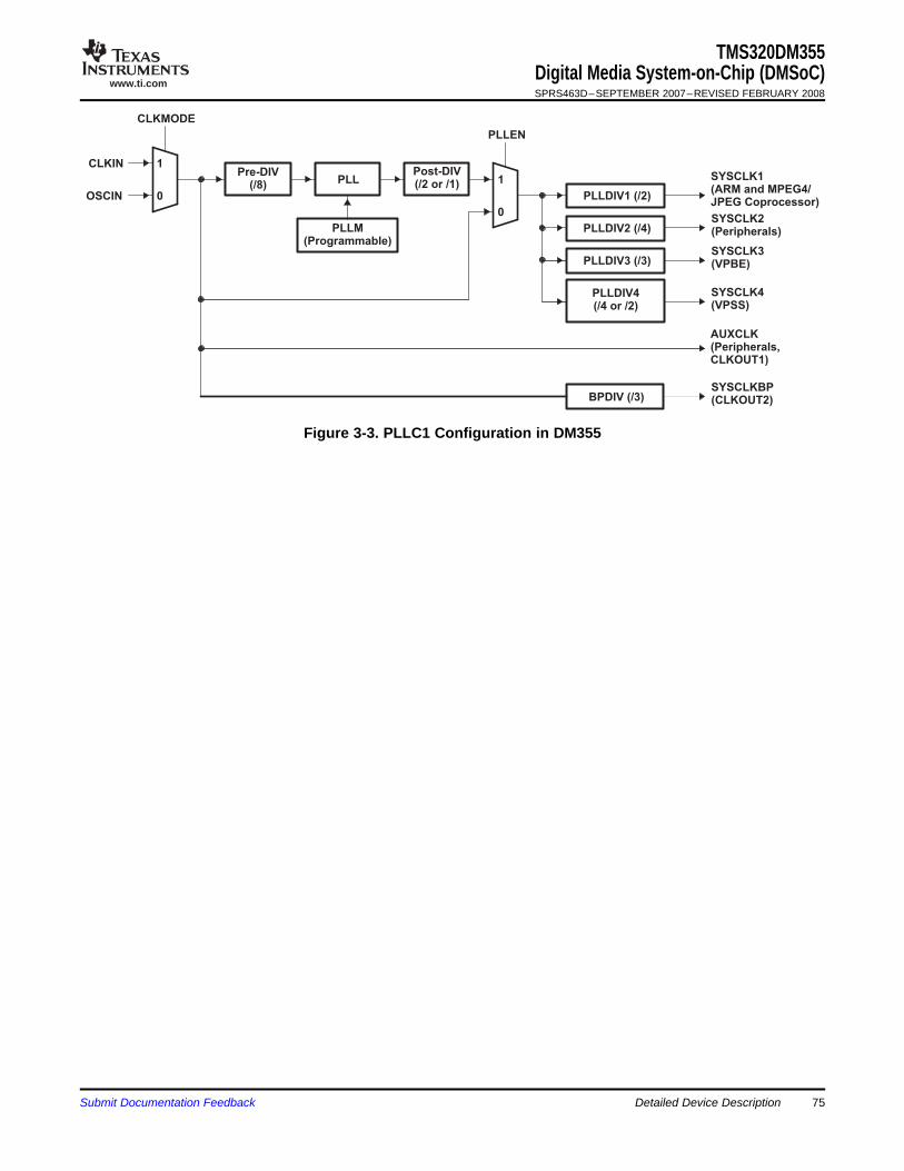
www.ti.com
PLLDIV1 (/2)
PLLDIV2 (/4)
PLLDIV3 (/3)
SYSCLK1(ARM and MPEG4/JPEG Coprocessor)
SYSCLK2(Peripherals)
SYSCLK3(VPBE)
1
0
PLL
0
1
CLKMODE
CLKIN
OSCIN
PLLEN
AUXCLK(Peripherals,CLKOUT1)
SYSCLKBP(CLKOUT2)
Pre-DIV(/8)
Post-DIV(/2 or /1)
PLLM(Programmable)
BPDIV (/3)
PLLDIV4(/4 or /2)
SYSCLK4(VPSS)
TMS320DM355Digital Media System-on-Chip (DMSoC)SPRS463D–SEPTEMBER 2007–REVISED FEBRUARY 2008
Figure 3-3. PLLC1 Configuration in DM355
Submit Documentation Feedback Detailed Device Description 75

www.ti.com
3.6.3 PLLC2
PLLDIV1 (/1)
1
0
PLL
0
1
CLKMODE
CLKIN
OSCIN
PLLEN
SYSCLK1
(DDR PHY)
SYSCLKBP
(CLKOUT3)BPDIV (/8)
PLLM(Programmable)
Pre-DIV(Programmable)
Post-DIV(/1)
TMS320DM355Digital Media System-on-Chip (DMSoC)SPRS463D–SEPTEMBER 2007–REVISED FEBRUARY 2008
PLLC2 provides the DDR PHY clock and CLKOUT3. Software controls PLLC2 operation through thePLLC2 registers. The following list, Table 3-11, and Figure 3-4 describe the customizations of PLLC2 inthe DM355.• Provides DDR PHY clock and CLKOUT3• Software configurable• Accepts clock input or internal oscillator input (same input as PLLC1)• PLL pre-divider value is programmable• PLL multiplier value is programmable• PLL post-divider value is fixed to (/1)• Only SYSCLK[1] is used• SYSCLK1 divider value is fixed to (/1)• SYSCLKBP divider value is fixed to (/8)• SYSCLK1 is routed to the DDR PHY• SYSCLKBP is routed to the output pin CLKOUT3• AUXCLK is not used.
Table 3-11. PLLC2 Output ClocksOutput Clock Used by PLLDIV Divider Notes
SYSCLK1 DDR PHY /1 Fixed dividerSYSCLKBP CLKOUT3 /8 Fixed divider
Figure 3-4. PLLC2 Configuration in DM355
Detailed Device Description76 Submit Documentation Feedback

www.ti.com
3.7 Power and Sleep Controller (PSC)
arm_clock
arm_mreset
arm_power
AINTC
ARM
module_power
module_mreset
MODxmodule_clock
Always on
domain
Interrupt
PSC
clksPLLC
Emulation
RESET
VDD
DMSoC
3.8 System Control Module
TMS320DM355Digital Media System-on-Chip (DMSoC)SPRS463D–SEPTEMBER 2007–REVISED FEBRUARY 2008
In the DM355 system, the Power and Sleep Controller (PSC) is responsible for managing transitions ofsystem power on/off, clock on/off, and reset. A block diagram of the PSC is shown in Figure 3-5. Many ofthe operations of the PSC are transparent to software, such as power-on-reset operations. However, thePSC provides you with an interface to control several important clock and reset operations.
The PSC includes the following features:• Manages chip power-on/off, clock on/off, and resets• Provides a software interface to:
– Control module clock ON/OFF– Control module resets
• Supports IcePick emulation features: power, clock, and reset
For more information on the PSC, see the TMS320DM35x Digital Media System-on-Chip (DMSoC) ARMSubsystem Reference Guide (literature number SPRUFB3) .
Figure 3-5. DM355 Power and Sleep Controller (PSC)
The DM355’s system control module is a system-level module containing status and top-level control logicrequired by the device. The system control module consists of a miscellaneous set of status and controlregisters, accessible by the ARM and supporting all of the following system features and operations:• Device identification• Device configuration
– Pin multiplexing control– Device boot configuration status
• ARM interrupt and EDMA event multiplexing control• Special peripheral status and control
– Timer64+– USB PHY control– VPSS clock and video DAC control and status– DDR VTP control– Clockout circuitry– GIO de-bounce control
Submit Documentation Feedback Detailed Device Description 77

www.ti.com
3.9 Pin Multiplexing
3.9.1 Hardware Controlled Pin Multiplexing
TMS320DM355Digital Media System-on-Chip (DMSoC)SPRS463D–SEPTEMBER 2007–REVISED FEBRUARY 2008
• Power management– Deep sleep and fast NAND boot control
• Bandwidth Management– Bus master DMA priority controlFor more information on the System Control Module refer to TMS320DM35x Digital MediaSystem-on-Chip (DMSoC) ARM Subsystem Reference Guide (literature number SPRUFB3) .
The DM355 makes extensive use of pin multiplexing to accommodate the large number of peripheralfunctions in the smallest possible package. In order to accomplish this, pin multiplexing is controlled usinga combination of hardware configuration (at device reset) and software control. No attempt is made by theDM355 hardware to ensure that the proper pin muxing has been selected for the peripherals or interfacemode being used, thus proper pin muxing configuration is the responsibility of the board and softwaredesigners. An overview of the pin multiplexing is shown in Table 3-12.
Table 3-12. Peripheral Pin Mux OverviewPeripheral Muxed With Primary Function Secondary Function Tertiary FunctionVPFE (video in) GPIO and SPI2 VPFE (video in) SPI2 GPIOVPBE (video out) GPIO, PWM, and RTO VPBE (video out) PWM and RTO GPIOAEMIF GPIO AEMIF GPIO noneASP0 GPIO ASP0 GPIO noneMMC/SD1 GPIO and UART2 MMC/SD1 GPIO UART2CLKOUT GPIO CLKOUT GPIO noneI2C GPIO I2C GPIO noneUART1 GPIO UART1 GPIO noneSPI1 GPIO SPI1 GPIO noneSPI0 GPIO SPI0 GPIO none
Use the Asynchronous EMIF configuration pins (AECFG[3:0]) for hardware pin mux control. AECFG[3:0]control the partitioning of the AEMIF addresses and GPIOs at reset, which allows you to properlyconfigure the number of AEMIF address pins required by the boot device while unused addresses pins areavailable as GPIOs. These settings may be changed by software after reset by programming the PinMux2register The PinMux2 register is in the System Control Module. As shown in Table 3-13, the number ofaddress bits enabled on the AEMIF is selectable from 0 to 16. Pins that are not assigned to anotherperipheral and not enabled as address signals become GPIOs (except EM_A[2:1]). The enabled addresssignals are always contiguous from EM_BA[1] upwards; bits cannot be skipped. The exception to this areEM_A[2:1]. These signals (can be used to) represent the ALE and CLE signals for the NAND Flash modeof the AEMIF and are always enabled. Note that EM_A[0] does not represent the lowest AEMIF addressbit. DM355 supports only 16-bit and 8-bit data widths for the AEMIF. In 16-bit mode, EM_BA[1] representsthe LS address bit (the half-word address) and EM_BA[0] represents the MS address bit (A[14]). In 8-bitmode, EM_BA[1:0] represent the 2 LS address bits. Note that additional selections are available byprogramming the PinMux2 register in software after boot. Note that AECFG selection of ‘0010’ selectsOneNAND interface. The AEMIF needs to operate in the half-rate mode (full_rate = 0) to meet frequencyrequirements. Software should not change the PINMUX2 register setting to affect the AEMIF rateoperation. A soft reset of the AEMIF should be performed any time a rate change is made.
Detailed Device Description78 Submit Documentation Feedback

www.ti.com
3.9.2 Software Controlled Pin Multiplexing
3.10 Device Reset
TMS320DM355Digital Media System-on-Chip (DMSoC)SPRS463D–SEPTEMBER 2007–REVISED FEBRUARY 2008
Table 3-13. AECFG (Async EMIF Configuration) Pin Mux Coding1101(NAND) 1100 1010 (OneNAND) 1000 (8-bit SRAM) 0010 (16-bit SRAM) 0000
GPIO[54] GPIO[54] EM_A[14] EM_BA[0] EM_A[14] EM_BA[0]GPIO[55] EM_BA[1] EM_BA[1] EM_BA[1] EM_BA[1] EM_BA[1]GPIO[56] EM_A[0] EM_A[0] EM_A[0] EM_A[0] EM_A[0]EM_A[1] EM_A[1] EM_A[1] EM_A[1] EM_A[1] EM_A[1]EM_A[2] EM_A[2] EM_A[2] EM_A[2] EM_A[2] EM_A[2]GPIO[57] EM_A[3] EM_A[3] EM_A[3] EM_A[3] EM_A[3]GPIO[58] EM_A[4] EM_A[4] EM_A[4] EM_A[4] EM_A[4]GPIO[59] EM_A[5] EM_A[5] EM_A[5] EM_A[5] EM_A[5]GPIO[60] EM_A[6] EM_A[6] EM_A[6] EM_A[6] EM_A[6]GPIO[61] EM_A[7] EM_A[7] EM_A[7] EM_A[7] EM_A[7]GPIO[62] EM_A[8] EM_A[8] EM_A[8] EM_A[8] EM_A[8]GPIO[63] EM_A[9] EM_A[9] EM_A[9] EM_A[9] EM_A[9]GPIO[64] EM_A[10] EM_A[10] EM_A[10] EM_A[10] EM_A[10]GPIO[65] EM_A[11] EM_A[11] EM_A[11] EM_A[11] EM_A[11]GPIO[66] EM_A[12] EM_A[12] EM_A[12] EM_A[12] EM_A[12]GPIO[67] EM_A[13] EM_A[13] EM_A[13] EM_A[13] EM_A[13]GPIO[46] GPIO[46] GPIO[46] GPIO[46] EM_D[8] EM_D[8]GPIO[47] GPIO[47] GPIO[47] GPIO[47] EM_D[9] EM_D[9]GPIO[48] GPIO[48] GPIO[48] GPIO[48] EM_D[10] EM_D[10]GPIO[49] GPIO[49] GPIO[49] GPIO[49] EM_D[11] EM_D[11]GPIO[50] GPIO[50] GPIO[50] GPIO[50] EM_D[12] EM_D[12]GPIO[51] GPIO[51] GPIO[51] GPIO[51] EM_D[13] EM_D[13]GPIO[52] GPIO[52] GPIO[52] GPIO[52] EM_D[14] EM_D[14]GPIO[53] GPIO[53] GPIO[53] GPIO[53] EM_D[15] EM_D[15]
All pin multiplexing options are configurable by software via pin mux registers that reside in the SystemControl Module. The PinMux0 Register controls the Video In muxing, PinMux1 register controls Video Outsignals, PinMux2 register controls AEMIF signals, PinMux3 registers control the multiplexing of the GIOsignals, the PinMux4 register controls the SPI and MMC/SD0 signals. Refer to TMS320DM35x DigitalMedia System-on-Chip (DMSoC) ARM Subsystem Reference Guide (literature numberSPRUFB3) forcomplete descriptions of the pin mux registers.
There are five types of reset in DM355. The types of reset differ by how they are initiated and/or by theireffect on the chip. Each type is briefly described in Table 3-14 and further described in TMS320DM35xDigital Media System-on-Chip (DMSoC) ARM Subsystem Reference Guide (literature number SPRUFB3).
Table 3-14. Reset TypesType Initiator EffectPOR (Power-On-Reset) RESET pin low and TRST low Total reset of the chip (cold reset). Resets all modules
including memory and emulation.Warm Reset RESET pin low and TRST high (initiated by ARM Resets all modules including memory, except ARM
emulator). emulation.Max Reset ARM emulator or Watchdog Timer (WDT). Same effect as warm reset.System Reset ARM emulator Resets all modules except memory and ARM
emulation. It is a soft reset that maintains memorycontents and does not affect or reset clocks or powerstates.
Submit Documentation Feedback Detailed Device Description 79

www.ti.com
3.11 Default Device Configurations
3.11.1 Device Configuration Pins
TMS320DM355Digital Media System-on-Chip (DMSoC)SPRS463D–SEPTEMBER 2007–REVISED FEBRUARY 2008
Table 3-14. Reset Types (continued)Type Initiator EffectModule Reset ARM software Resets a specific module. Allows the ARM to
independently reset any module. Module reset isintended as a debug tool not as a tool to use inproduction.
After POR, warm reset, and max reset, the chip is in its default configuration. This section highlights thedefault configurations associated with PLLs, clocks, ARM boot mode, and AEMIF.
NOTEDefault configuration is the configuration immediately after POR, warm reset, and maxreset and just before the boot process begins. The boot ROM updates the configuration.See Section 3.12 for more information on the boot process.
The device configuration pins are described in Table 3-15. The device configuration pins are latched atreset and allow you to configure all of the following options at reset:• ARM Boot Mode• Asynchronous EMIF pin configuration
These pins are described further in the following sections.
NOTEThe device configuration pins are multiplexed with AEMIF pins. After the deviceconfiguration pins are sampled at reset, they automatically change to function as AEMIFpins. Pin multiplexing is described in Section 3.8.
Table 3-15. Device ConfigurationDefault Setting (by
internalDevice Sampled pull-up/
Configuration Input Function Pin pull-down) Device Configuration AffectedBTSEL[1:0] Selects ARM boot mode EM_A[13:12] 00 If any ROM boot mode is selected, GIO61
00 = Boot from ROM (NAND) (NAND) is used to indicated boot status.01 = Boot from AEMIF If NAND boot is selected, CE0 is used for10 = Boot from ROM NAND. Use AECFG[3:0] to configure(MMC/SD) AEMIF pins for NAND.11 = Boot from ROM (UART) If AEMIF boot is selected, CE0 is used for
AEMIF device (OneNAND, ROM). UseAECFG[3:0] to configure AEMIF pins forNAND.If MMC/SD boot is selected, MMC/SD0 isused.
AECFG[3:0] Selects AEMIF pin EM_A[11:8] 1101 Selects the AEMIF pin configuration. Referconfiguration (NAND) to pin-muxing information in Section 3.9.1.
Note that AECFG[3:0] affects both AEMIF(BTSEL[1:0]=01) and NAND(BTSEL[1:0]=00) boot modes.
Detailed Device Description80 Submit Documentation Feedback

www.ti.com
3.11.2 PLL Configuration
3.11.3 Power Domain and Module State Configuration
TMS320DM355Digital Media System-on-Chip (DMSoC)SPRS463D–SEPTEMBER 2007–REVISED FEBRUARY 2008
After POR, warm reset, and max reset, the PLLs and clocks are set to their default configurations. ThePLLs are in bypass mode and disabled by default. This means that the input reference clock at MXI1(typically 24 MHz) drives the chip after reset. For more information on device clocking, see Section 3.5and Section 3.6. The default state of the PLLs is reflected in the default state of the register bits in thePLLC registers. Refer to TMS320DM35x Digital Media System-on-Chip (DMSoC) ARM SubsystemReference Guide (literature number SPRUFB3) for PLLC register descriptions.
Only a subset of modules are enabled after reset by default. Table 3-16 shows which modules areenabled after reset. Table 3-16 as shows that the following modules are enabled depending on thesampled state of the device configuration pins: EDMA (CC and TC0), AEMIF, MMC/SD0, UART0, andTimer0. For example, UART0 is enabled after reset when the device configuration pins (BTSEL[1:0] = 11 -Enable UART) select UART boot mode. For more information on module configuration refer to .
Submit Documentation Feedback Detailed Device Description 81

www.ti.com
TMS320DM355Digital Media System-on-Chip (DMSoC)SPRS463D–SEPTEMBER 2007–REVISED FEBRUARY 2008
Table 3-16. Module ConfigurationDefault States
Module Module Name Power Domain Power Domain State Module StateNumber
0 VPSS Master AlwaysOn ON SyncRst1 VPSS Slave AlwaysOn ON SyncRst2 EDMA (CC) AlwaysOn ON BTSEL[1:0] = 00 – Enable (NAND)
BTSEL[1:0] = 01 – Enable (OneNAND)3 EDMA (TC0) AlwaysOn ON BTSEL[1:0] = 10 – SyncRst (MMC/SD)
BTSEL[1:0] = 11 – Enable (UART)4 EDMA (TC1) AlwaysOn ON SyncRst5 Timer3 AlwaysOn ON SyncRst6 SPI1 AlwaysOn ON SyncRst7 MMC/SD1 AlwaysOn ON SyncRst8 ASP1 AlwaysOn ON SyncRst9 USB AlwaysOn ON SyncRst10 PWM3 AlwaysOn ON SyncRst11 SPI2 AlwaysOn ON SyncRst12 RTO AlwaysOn ON SyncRst13 DDR EMIF AlwaysOn ON SyncRst14 AEMIF AlwaysOn ON BTSEL[1:0] = 00 – Enable (NAND)
BTSEL[1:0] = 01 – Enable (OneNAND)BTSEL[1:0] = 10 – SyncRst (MMC/SD)BTSEL[1:0] = 11 – Enable (UART)
15 MMC/SD0 AlwaysOn ON BTSEL[1:0] = 00 – Enable (NAND)BTSEL[1:0] = 01 – Enable (OneNAND)BTSEL[1:0] = 10 – SyncRst (MMC/SD)BTSEL[1:0] = 11 – Enable (UART)
16 Reserved17 ASP AlwaysOn ON SyncRst18 I2C AlwaysOn ON SyncRst19 UART0 AlwaysOn ON BTSEL[1:0] = 00 – Enable (NAND)
BTSEL[1:0] = 01 – Enable (OneNAND)BTSEL[1:0] = 10 – SyncRst (MMC/SD)BTSEL[1:0] = 11 – Enable (UART)
20 UART1 AlwaysOn ON SyncRst21 UART2 AlwaysOn ON SyncRst22 SPI0 AlwaysOn ON SyncRst23 PWM0 AlwaysOn ON SyncRst24 PWM1 AlwaysOn ON SyncRst25 PWM2 AlwaysOn ON SyncRst26 GPIO AlwaysOn ON SyncRst27 TIMER0 AlwaysOn ON BTSEL[1:0] = 00 – Enable (NAND)
BTSEL[1:0] = 01 – Enable (OneNAND)BTSEL[1:0] = 10 – SyncRst (MMC/SD)BTSEL[1:0] = 11 – Enable (UART)
28 TIMER1 AlwaysOn ON SyncRst29 TIMER2 AlwaysOn ON Enable30 System Module AlwaysOn ON Enable
Detailed Device Description82 Submit Documentation Feedback

www.ti.com
3.11.4 ARM Boot Mode Configuration
3.11.5 AEMIF Configuration
3.11.5.1 AEMIF Pin Configuration
3.11.5.2 AEMIF Timing Configuration
3.12 Device Boot Modes
TMS320DM355Digital Media System-on-Chip (DMSoC)SPRS463D–SEPTEMBER 2007–REVISED FEBRUARY 2008
Table 3-16. Module Configuration (continued)Default States
31 ARM AlwaysOn ON Enable32 BUS AlwaysOn ON Enable33 BUS AlwaysOn ON Enable34 BUS AlwaysOn ON Enable35 BUS AlwaysOn ON Enable36 BUS AlwaysOn ON Enable37 BUS AlwaysOn ON Enable38 BUS AlwaysOn ON Enable39 Reserved Reserved Reserved Reserved40 VPSS DAC Always On ON SyncRst
The input pins BTSEL[1:0] determine whether the ARM will boot from its ROM or from the AsynchronousEMIF (AEMIF). When ROM boot is selected (BTSEL[1:0] = 00, 10, or 11), a jump to the start of internalROM (address 0x0000: 8000) is forced into the first fetched instruction word. The embedded ROM bootloader code (RBL) then performs certain configuration steps, reads the BOOTCFG register to determinethe desired boot method, and branches to the appropriate boot routine (i.e., a NAND, MMC/SD, or UARTloader routine).
If AEMIF boot is selected (BTSEL[1:0] = 01), a jump to the start of AEMIF (address 0x0200: 0000) isforced into the first fetched instruction word. The ARM then continues executing from externalasynchronous memory using the default AEMIF timings until modified by software.
NOTEFor AEMIF boot, the OneNAND must be connected to the first AEMIF chip select space(EM_CE0). Also, the AEMIF does not support direct execution from NAND Flash.
Boot modes are further described in Section 3.12.
The input pins AECFG[3:0] determine the AEMIF configuration immediately after reset. Use AECFG[3:0]to properly configure the pins of the AEMIF. Refer to the section on pin multiplexing in Section 3.9.
Also, see the Asynchronous External Memory Interface (AEMIF) Peripheral Reference Guide (SPRUEE8)for more information on the AEMIF.
When AEMIF is enabled, the wait state registers are reset to the slowest possible configuration, which is88 cycles per access (16 cycles of setup, 64 cycles of strobe, and 8 cycles of hold). Thus, with a 24 MHzclock at MXI1, the AEMIF is configured to run at 6 MHz/88 which equals approximately 68 kHz by default.See the Asynchronous External Memory Interface (AEMIF) Peripheral Reference Guide for moreinformation on the AEMIF.
The DM355 ARM can boot from either Async EMIF (AEMIF/OneNand) or from ARM ROM, as determinedby the setting of the device configuration pins BTSEL[1:0]. The BTSEL[1:0] pins can define the ROM bootmode further as well.
Submit Documentation Feedback Detailed Device Description 83

www.ti.com
3.12.1 Boot Modes Overview
TMS320DM355Digital Media System-on-Chip (DMSoC)SPRS463D–SEPTEMBER 2007–REVISED FEBRUARY 2008
The boot selection pins (BTSEL[1:0]) determine the ARM boot process. After reset (POR, warm reset, ormax reset), ARM program execution begins in ARM ROM at 0x0000: 8000, except when BTSEL[1:0] = 01,indicating AEMIF (AEMIF/OneNand) boot. See Section 3.11.1 for information on the boot selection pins.
DM355’s ARM ROM boot loader (RBL) executes when the BOOTSEL[1:0] pins indicate a condition otherthan the normal ARM EMIF boot.• If BTSEL[1:0] = 01 - Asynchronous EMIF (AEMIF) boot. This mode is handled by hardware control and
does not involve the ROM. In the case of OneNAND, the user is responsible for putting any necessaryboot code in the OneNAND's boot page. This code shall configure the AEMIF module for theOneNAND device. After the AEMIF module is configured, booting will continue immediately after theOneNAND’s boot page with the AEMIF module managing pages thereafter. Furthermore, in case ofFast Boot from AEMIF/OneNAND, the user is responsible for checking the state of the FASTBOOT bitin the BOOTCFG register in the System Module in order to respond properly by executing any requireddevice init, bringing mDDR out of self-refresh, and branching to user entry point in mDDR.
• The RBL supports 3 distinct boot modes:– BTSEL[1:0] = 00 - ARM NAND Boot– BTSEL[1:0] = 10 - ARM MMC/SD Boot– BTSEL[1:0] = 11 - ARM UART Boot
• If NAND boot fails, then MMC/SD mode is tried.• If MMC/SD boot fails, then MMC/SD boot is tried again.• If UART boot fails, then UART boot is tried again.• RBL uses GIO61 to indicate boot status (can use to blink LED):
– After reset, GIO61 is initially driven low (e.g LED off)– If NAND boot fails and then MMC/SD boot fails, then GIO61 shall toggle at 4Hz while MMC/SD
boot is retried.– If MMC/SD boot fails, then GIO61 shall toggle at 4Hz while MMC/SD boot is retried– If UART boot fails, then GIO61 shall toggle at 2Hz while UART boot is retried– When boot is successful, just before program control is given to UBL, GIO61 is driven high (e.g.
LED on)– DM355 Timer0 shall be used to accurately toggle GIO61 at 4Hz and 2Hz
• ARM ROM Boot - NAND Mode– No support for a full firmware boot. Instead, copies a second stage user boot loader (UBL) from
NAND flash to ARM internal RAM (AIM) and transfers control to the user-defined UBL.– Support for NAND with page sizes up to 2048 bytes.– Support for magic number error detection and retry (up to 24 times) when loading UBL– Support for up to 30KB UBL (32KB IRAM - ~2KB for RBL stack)– Optional, user-selectable, support for use of DMA and I-cache during RBL execution (i.e.,while
loading UBL)– Supports booting from 8-bit NAND devices (16-bit NAND devices are not supported)– Supports 4-bit ECC (1-bit ECC is not supported)– Supports NAND flash that requires chip select to stay low during the tR read time– Supports Fast Boot option, which allows you to quickly boot and recover from a low power mode
• ARM ROM Boot - MMC/SD Mode– No support for a full firmware boot. Instead, copies a second stage Uwer Boot Loader (UBL) from
MMC/SD to ARm Internal RAM (AIM) and transfers control to the user software.– Support for MMC/SD Native protocol (MMC/SD SPI protocol is not supported)– Support for descriptor error detection and retry (up to 24 times) when loading UBL– Support for up to 30KB UBL (32KB - ~2KB for RBL stack)
Detailed Device Description84 Submit Documentation Feedback

www.ti.com
Bootmode
?
Reset
Bootmode
?
Boot fromNAND flash
Internal ROM
Boot OK ? No
Yes
Boot fromUART
Boot fromMMC/SD
Boot OK ?
Boot OK ?
Yes
No
Invoke loadedProgram
InvokeOneNAND
No
Yes
3.13 Power Management
TMS320DM355Digital Media System-on-Chip (DMSoC)SPRS463D–SEPTEMBER 2007–REVISED FEBRUARY 2008
• ARM ROM Boot - UART mode– No support for a full firmware boot. Instead, loads a second stage user boot loader (UBL) via UART
to ARM internal RAM (AIM) and transfers control to the user software.– Support for up to 30KB UBL (32KB - ~2KB for RBL stack)
The general boot sequence is shown in Figure 3-6. For more information, refer to TMS320DM35x DigitalMedia System-on-Chip (DMSoC) ARM Subsystem Reference Guide (literature number SPRUFB3) .
Figure 3-6. Boot Mode Functional Block Diagram
The DM355 is designed for minimal power consumption. There are two components to powerconsumption: active power and leakage power. Active power is the power consumed to perform work andscales with clock frequency and the amount of computations being performed. Active power can bereduced by controlling the clocks in such a way as to either operate at a clock setting just high enough tocomplete the required operation in the required timeline or to run at a clock setting until the work iscomplete and then drastically cut the clocks (e.g. to PLL Bypass mode) until additional work must beperformed. Leakage power is due to static current leakage and occurs regardless of the clock rate.
Submit Documentation Feedback Detailed Device Description 85

www.ti.com
TMS320DM355Digital Media System-on-Chip (DMSoC)SPRS463D–SEPTEMBER 2007–REVISED FEBRUARY 2008
Leakage, or standby power, is unavoidable while power is applied and scales roughly with the operatingjunction temperatures. Leakage power can only be avoided by removing power completely from a deviceor subsystem. The DM355 includes several power management features which are briefly described inTable 3-17. Refer to TMS320DM35x Digital Media System-on-Chip (DMSoC) ARM Subsystem ReferenceGuide (literature number SPRUFB3) for more information on power management.
Table 3-17. Power Management FeaturesPower Management Features Description
Clock ManagementModule clock disable Module clocks can be disabled to reduce switching powerModule clock frequency scaling Module clock frequency can be scaled to reduce switching powerPLL power-down The PLLs can be powered-down when not in use to reduce
switching powerARM Sleep Mode
ARM Wait-for-Interrupt sleep mode Disable ARM clock to reduce active powerSystem Sleep Modes
Deep Sleep mode Stop all device clocks and power down internal oscillators to reduceactive power to a minimum. Registers and memory are preserved.
I/O ManagementUSB Phy power-down The USB Phy can be powered-down to reduce USB I/O powerDAC power-down The DAC's can be powered-down to reduce DAC powerDDR self-refresh and power down The DDR / mDDR device can be put into self-refresh and power
down states
Detailed Device Description86 Submit Documentation Feedback

www.ti.com
3.14 64-Bit Crossbar Architecture
3.14.1 Crossbar Connections
3.14.2 EDMA Controller
TMS320DM355Digital Media System-on-Chip (DMSoC)SPRS463D–SEPTEMBER 2007–REVISED FEBRUARY 2008
The DM355 uses a 64-bit crossbar architecture to control access between device processors, subsystemsand peripherals. It includes an EDMA Controller consisting of a DMA Transfer Controller (TC) and a DMAChannel Controller (CC). The TC provides two DMA channels for transfer between slave peripherals. TheCC provides a user and event interface to the EDMA system. It includes up to 64 event channels to whichall system synchronization events can be mapped and 8 auto submit “quick” channels (QDMA). In mostways, these channels are identical. A channel refers to a specific ‘event’ that can cause a transfer to besubmitted to the TC as a Transfer Request.
There are five transfer masters (TCs have separate read and write connections) connected to thecrossbar; ARM, the Video Processing Sub-system (VPSS), the master peripherals (USB), and two EDMAtransfer controllers. These can be connected to four separate slave ports; ARM, the DDR EMIF, and CFGbus peripherals. Not all masters may connect to all slaves. Connection paths are indicated by √ atintersection points shown in Table 3-18
Table 3-18. Crossbar Connection MatrixSlave Module
DMA Master ARM Internal MPEG4/JPEG Config Bus Registers and DDR EMIF MemoryMemory Coprocessor Memory
MemoryARM √ √ √ √
VPSS √
DMA Master Peripherals (USB) √ √
EDMA3TC0 √ √ √ √
EDMA3TC1 √ √ √ √
The EDMA controller handles all data transfers between memories and the device slave peripherals onthe DM355 device. These are summarized as follows:• Transfer to/from on-chip memories
– ARM program/data RAM– MPEG4/JPEG Coprocessor memory
• Transfer to/from external storage– DDR2 / mDDR SDRAM– Asynchronous EMIF– OneNAND flash– NAND flash– Smart Media, SD, MMC, xD media storage
• Transfer to/from peripherals– ASP– SPI– I2C– PWM– RTO– GPIO– Timer/WDT– UART– MMC/SD
Submit Documentation Feedback Detailed Device Description 87

www.ti.com
TMS320DM355Digital Media System-on-Chip (DMSoC)SPRS463D–SEPTEMBER 2007–REVISED FEBRUARY 2008
The EDMA Controller consists of two major blocks: the Transfer Controller (TC) and the ChannelController (CC). The CC is a highly flexible Channel Controller that serves as the user interface and eventinterface for the EDMA system. The CC supports 64-event channels and 8 QDMA channels. The CCconsists of a scalable Parameter RAM (PaRAM) that supports flexible ping-pong, circular buffering,channel-chaining, auto-reloading, and memory protection.
The EDMA Channel Controller has the following features:• Fully orthogonal transfer description
– Three transfer dimensions– A-synchronized transfers: one dimension serviced per event– AB- synchronized transfers: two dimensions serviced per event– Independent indexes on source and destination– Chaining feature allows 3-D transfer based on single event
• Flexible transfer definition– Increment and constant addressing modes– Linking mechanism allows automatic PaRAM set update– Chaining allows multiple transfers to execute with one event
• Interrupt generation for:– DMA completion– Error conditions
• Debug visibility– Queue watermarking/threshold– Error and status recording to facilitate debug
• 64 DMA channels– Event synchronization– Manual synchronization (CPU(s) write to event set register)– Chain synchronization (completion of one transfer chains to next)
• 8 QDMA channels– QDMA channels are triggered automatically upon writing to a PaRAM set entry– Support for programmable QDMA channel to PaRAM mapping
• 128 PaRAM sets– Each PaRAM set can be used for a DMA channel, QDMA channel, or link set (remaining)
• Two transfer controllers/event queues. The system-level priority of these queues is user programmable• 16 event entries per event queue• External events (for example, ASP TX Evt and RX Evt)The EDMA Transfer Controller has the following features:
• Two transfer controllers• 64-bit wide read and write ports per channel• Up to four in-flight transfer requests (TR)• Programmable priority level• Supports two dimensional transfers with independent indexes on source and destination (EDMA3CC
manages the 3rd dimension)• Support for increment and constant addressing modes• Interrupt and error support
Parameter RAM: Each EDMA is specified by an eight word (32-byte) parameter table contained inParameter RAM (PaRAM) within the CC. DM355 provides 128 PaRAM entries, one for each of the 64DMA channels and for 64 QDMA / Linked DMA entries.
Detailed Device Description88 Submit Documentation Feedback

www.ti.com
3.14.2.1 EDMA Channel Synchronization Events
TMS320DM355Digital Media System-on-Chip (DMSoC)SPRS463D–SEPTEMBER 2007–REVISED FEBRUARY 2008
DMA Channels: Can be triggered by: " External events (for example, ASP TX Evt and RX Evt), " Softwarewriting a '1' to the given bit location, or channel, of the Event Set register, or, " Chaining to other DMAs.
QDMA: The Quick DMA (QDMA) function is contained within the CC. DM355 implements 8 QDMAchannels. Each QDMA channel has a selectable PaRAM entry used to specify the transfer. A QDMAtransfer is submitted immediately upon writing of the "trigger" parameter (as opposed to the occurrence ofan event as with EDMA). The QDMA parameter RAM may be written by any Config bus master throughthe Config Bus and by DMAs through the Config Bus bridge.
QDMA Channels: Triggered by a configuration bus write to a designated 'QDMA trigger word'. QDMAsallow a minimum number of linear writes (optimized for GEM IDMA feature) to be issued to the CC toforce a series of transfers to take place.
The EDMA supports up to 64 EDMA channels which service peripheral devices and external memory.Table 3-19 lists the source of EDMA synchronization events associated with each of the programmableEDMA channels. For the DM355 device, the association of an event to a channel is fixed; each of theEDMA channels has one specific event associated with it. These specific events are captured in theEDMA event registers (ER, ERH) even if the events are disabled by the EDMA event enable registers(EER, EERH). For more detailed information on the EDMA module and how EDMA events are enabled,captured, processed, linked, chained, and cleared, etc., see the Document Support section for theEnhanced Direct Memory Access (EDMA) Controller Reference Guide.
Table 3-19. DM355 EDMA Channel Synchronization Events (1) (2)
EDMA EVENT NAME EVENT DESCRIPTIONCHANNEL0 TIMER3: TINT6 Timer 3 Interrupt (TINT6) Event1 TIMER3 TINT7 Timer 3 Interrupt (TINT7) Event2 ASP0: XEVT ASP0 Transmit Event3 ASP0: REVT ASP0 Receive Event4 VPSS: EVT1 VPSS Event 15 VPSS: EVT2 VPSS Event 26 VPSS: EVT3 VPSS Event 37 VPSS: EVT4 VPSS Event 4
ASP1: XEVT or TIMER2:8 ASP1 Transmit Event or Timer 2 interrupt (TINT4) EventTINT4ASP1: REVT or TIMER2:9 ASP1 Receive Event or Timer 2 interrupt (TINT5) EventTINT5
10 SPI2: SPI2XEVT SPI2 Transmit Event11 SPI2: SPI2REVT SPI2 Receive Event12 Reserved13 Reserved14 SPI1: SPI1XEVT SPI1 Transmit Event15 SPI1: SPI1REVT SPI1 Receive Event16 SPI0: SPI0XEVT SP0I Transmit Event17 SPI0: SPI0REVT SPI0 Receive Event18 UART0: URXEVT0 UART 0 Receive Event19 UART0: UTXEVT0 UART 0 Transmit Event
(1) In addition to the events shown in this table, each of the 64 channels can also be synchronized with the transfer completion orintermediate transfer completion events. For more detailed information on EDMA event-transfer chaining, see the Document Supportsection for the Enhanced Direct Memory Access (EDMA) Controller Reference Guide.
(2) The total number of EDMA events in DM355 exceeds 64, which is the maximum value of the EDMA module. Therefore, several eventsare multiplexed and you must use the register EDMA_EVTMUX in the System Control Module to select the event source for multiplexedevents. Refer to TMS320DM35x Digital Media System-on-Chip (DMSoC) ARM Subsystem Reference Guide (literature numberSPRUFB3) for more information on the System Control Module register EDMA_EVTMUX.
Submit Documentation Feedback Detailed Device Description 89
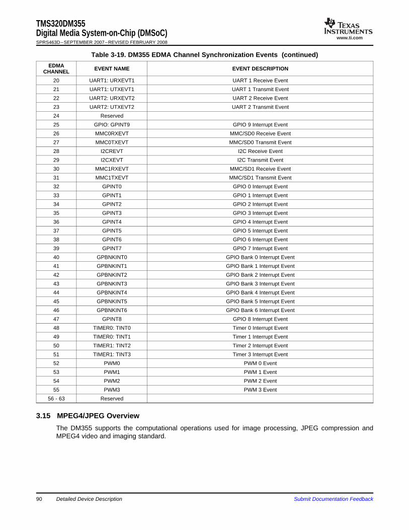
www.ti.com
3.15 MPEG4/JPEG Overview
TMS320DM355Digital Media System-on-Chip (DMSoC)SPRS463D–SEPTEMBER 2007–REVISED FEBRUARY 2008
Table 3-19. DM355 EDMA Channel Synchronization Events (continued)EDMA EVENT NAME EVENT DESCRIPTIONCHANNEL
20 UART1: URXEVT1 UART 1 Receive Event21 UART1: UTXEVT1 UART 1 Transmit Event22 UART2: URXEVT2 UART 2 Receive Event23 UART2: UTXEVT2 UART 2 Transmit Event24 Reserved25 GPIO: GPINT9 GPIO 9 Interrupt Event26 MMC0RXEVT MMC/SD0 Receive Event27 MMC0TXEVT MMC/SD0 Transmit Event28 I2CREVT I2C Receive Event29 I2CXEVT I2C Transmit Event30 MMC1RXEVT MMC/SD1 Receive Event31 MMC1TXEVT MMC/SD1 Transmit Event32 GPINT0 GPIO 0 Interrupt Event33 GPINT1 GPIO 1 Interrupt Event34 GPINT2 GPIO 2 Interrupt Event35 GPINT3 GPIO 3 Interrupt Event36 GPINT4 GPIO 4 Interrupt Event37 GPINT5 GPIO 5 Interrupt Event38 GPINT6 GPIO 6 Interrupt Event39 GPINT7 GPIO 7 Interrupt Event40 GPBNKINT0 GPIO Bank 0 Interrupt Event41 GPBNKINT1 GPIO Bank 1 Interrupt Event42 GPBNKINT2 GPIO Bank 2 Interrupt Event43 GPBNKINT3 GPIO Bank 3 Interrupt Event44 GPBNKINT4 GPIO Bank 4 Interrupt Event45 GPBNKINT5 GPIO Bank 5 Interrupt Event46 GPBNKINT6 GPIO Bank 6 Interrupt Event47 GPINT8 GPIO 8 Interrupt Event48 TIMER0: TINT0 Timer 0 Interrupt Event49 TIMER0: TINT1 Timer 1 Interrupt Event50 TIMER1: TINT2 Timer 2 Interrupt Event51 TIMER1: TINT3 Timer 3 Interrupt Event52 PWM0 PWM 0 Event53 PWM1 PWM 1 Event54 PWM2 PWM 2 Event55 PWM3 PWM 3 Event
56 - 63 Reserved
The DM355 supports the computational operations used for image processing, JPEG compression andMPEG4 video and imaging standard.
90 Detailed Device Description Submit Documentation Feedback

www.ti.com
4 Device Operating Conditions
4.1 Absolute Maximum Ratings Over Operating Case Temperature Range
TMS320DM355Digital Media System-on-Chip (DMSoC)SPRS463D–SEPTEMBER 2007–REVISED FEBRUARY 2008
(Unless Otherwise Noted) (1) (2)
All 1.3 V supplies -0.5 V to 1.7 VAll digital 1.8 V supplies -0.5 V to 2.5 V
Supply voltage rangesAll analog 1.8 V supplies -0.5 V to 1.89 VAll 3.3 V supplies -0.5 V to 4.4 VAll 1.8 V I/Os -0.5 V to 2.3 V
Input voltage ranges All 3.3 V I/Os -0.5 V to 3.8 VVBUS 0.0 V to 5.5 V
Clamp current for input or output (3) Iclamp -20 mA to 20 mAOperating case temperature ranges Tc -0°C to 85 °CStorage temperature ranges Tstg -65°C to 150 °C
(1) Stresses beyond those listed under "absolute maximum ratings" may cause permanent damage to the device. These are stress ratingsonly, and functional operation of the device at these or any other conditions beyond those indicated under "recommended operatingconditions" is not implied. Exposure to absolute-maximum-rated conditions for extended periods may affect device reliability.
(2) All voltage values are with respect to VSS.(3) Clamp current flows from an input or output pad to a supply rail through a clamp circuit or an intrinsic diode. Positive current results from
an applied input or output voltage that is more than 0.5 V higher (more positive) than the supply voltage,VDD/VDDA_PLL1/2/VDD_USB/VDD_DDR for dual-supply macros. Negative current results from an applied voltage that is more than 0.5 V less(more negative) than the VSS voltage..
Submit Documentation Feedback Device Operating Conditions 91

www.ti.com
4.2 Recommended Operating Conditions
TMS320DM355Digital Media System-on-Chip (DMSoC)SPRS463D–SEPTEMBER 2007–REVISED FEBRUARY 2008
MIN NOM MAX UNITCVDD Supply voltage, Core 1.235 1.3 1.365 VVDDA_PLL1 Supply voltage, PLL1 1.235 1.3 1.365 VVDDA_PLL2 Supply voltage, PLL2 1.235 1.3 1.365 VVDDD13_USB Supply voltage, USB Digital 1.235 1.3 1.365 VVDDA13_USB Supply voltage, USB Analog 1.235 1.3 1.365 VVDDA33_USB Supply voltage, USB Analog 3.135 3.3 3.465 V
Supply Voltage VDDA33_USB_PLL Supply voltage, USB Common PLL 3.135 3.3 3.465 VVDD_DDR Supply voltage, DDR2 / MDDR 1.71 1.8 1.89 VVDDA33_DDRDLL Supply voltage, DDR DLL Analog 3.135 3.3 3.465 VVDD_VIN Supply voltage, Digital video In 3.135 3.3 3.465 VVDD_VOUT Supply voltage, Digital Video Out 3.135 3.3 3.465 VVDDA18_DAC Supply voltage, DAC Analog 1.71 1.8 1.89 VVDD Supply voltage, I/Os 3.135 3.3 3.465 VVSS Supply ground, Core, USB Digital 0 0 0 VVSSA_PLL1 Supply ground, PLL1 0 0 0 VVSSA_PLL2 Supply ground, PLL2 0 0 0 VVSS_USB Supply ground, USB 0 0 0 V
Supply GroundVSSA_DLL Supply ground, DLL 0 0 0 VVSSA_DAC Supply ground, DAC Analog 0 0 0 VVSS_MX1 MXI1 osc ground (1) 0 0 0 VVSS_MX2 MXI2 osc ground (1) 0 0 0 V
Voltage Input High VIH High-level input voltage (2) 2 VVoltage Input Low VIL Low-level input voltage (2) 0.8 V
VREF DAC reference voltage 450 mVRBIAS DAC full-scale current adjust resistor 2550 Ω
DAC (3)RLOAD Output resistor 499 Ω
CBG Bypass capacitor 0.1 µFOutput resistor (ROUT), between TVOUT andROUT 1070VFB pins Ω
RFB Feedback resistor, between VFB and IOUT pins. 1000Video Buffer (3)
RBIAS DAC full-scale current adjust resistor 2550 Ω
CBG Bypass capacitor 0.1 µAUSB_VBUS USB external charge pump input 4.85 5 5.25 V
USBR1 USB reference resistor (4) 9.9 10 10.1 kΩ
Temperature Tc Operating case temperature rage 0 85 °C
(1) Oscillator ground must be kept separate from other grounds and connected directly to the crystal load capacitor ground (seeSection 5.5.1).
(2) These I/O specifications apply to regular 3.3 V I/Os and do not apply to DDR2/mDDR, USB I/Os. DDR2/mDDR I/Os are 1.8 V I/Os andadhere to JESD79-2A standard, USB I/Os adhere to USB2.0 spec.
(3) See Section 5.9.2.4. Also, resistors should be E-96 spec line (3 digits with 1% accuracy).(4) Connect USB_R1 to VSS_USB_REF via 10K ohm, 1% resistor placed as close to the device as possible.
Device Operating Conditions92 Submit Documentation Feedback

www.ti.com
4.3 Electrical Characteristics Over Recommended Ranges of Supply Voltage and Operating
TMS320DM355Digital Media System-on-Chip (DMSoC)SPRS463D–SEPTEMBER 2007–REVISED FEBRUARY 2008
Case Temperature (Unless Otherwise Noted)PARAMETER TEST CONDITIONS (1) MIN TYP MAX UNIT
VOH High-level output voltage (2) VDD=MIN, IOH=MAX 2.4Voltage VOutput VOL Low-level output voltage (2) VDD=MIN, IOL=MAX 0.6Input current for I/O withoutII VI = VSS to VDD -1 1internal pull-up/pull-downInput current for I/O with internalII(pullup) VI = VSS to VDD 40 190pull-up (3) (4)
Current Input current for I/O with internalII(pulldown) VI = VSS to VDD -190 -40Input/Outp µApull-down (3) (4)ut
IOH High-level output current -100IOL Low-level output current 4000
VO = VDD or VSS; internal pullIOZ I/O off-state output current ±10disabledCI Input capacitance 4Capacitan pFce CO Output capacitance 4Resolution Resolution 10 Bits
RLOAD = 499 Ω, Video bufferINL Integral non-linearity, best fit 1 LSBdisabledDAC
RLOAD = 499 Ω, Video bufferDNL Differential non-linearity 0.5 LSBdisabledCompliance Output compliance range IFS = 1.4 mA, RLOAD = 499 Ω 0 0.700 V
Output high voltage (top of 75%VOH(VIDBUF) 1.55NTSC or PAL colorbar) (5)Video VBuffer Outpupt low voltage (bottom ofVOL(VIDBUF) 0.470sync tip)
(1) For test conditions shown as MIN, MAX, or NOM, use the appropriate value specified in the recommended operating conditions table.(2) These I/O specifications apply to regular 3.3 V I/Os and do not apply to DDR2/mDDR, USB I/Os. DDR2/mDDR I/Os are 1.8 V I/Os and
adhere to JESD79-2A standard, USB I/Os adhere to USB2.0 spec.(3) This specification applies only to pins with an internal pullup (PU) or pulldown (PD). See Section 2.4 or Section 2.5 for pin descriptions.(4) To pull up a signal to the opposite supply rail, a 1 kΩ resistor is recommended.(5) 100% color bars are not supported. 100% color bars require 1.2 V peak-to-peak. The video buffer only provides 1.0 V peak-to-peak.
Submit Documentation Feedback Device Operating Conditions 93

www.ti.com
5 DM355 Peripheral Information and Electrical Specifications
5.1 Parameter Information Device-Specific Information
Transmission Line
4.0 pF 1.85 pF
Z0 = 50 Ω(see note)
Tester Pin Electronics Data Sheet Timing Reference Point
OutputUnderTest
42 Ω 3.5 nH
Device Pin(see note)
5.1.1 Signal Transition Levels
Vref
Vref = VIL MAX (or VOL MAX)
Vref = VIH MIN (or VOH MIN)
5.1.2 Timing Parameters and Board Routing Analysis
TMS320DM355Digital Media System-on-Chip (DMSoC)SPRS463D–SEPTEMBER 2007–REVISED FEBRUARY 2008
A. The data sheet provides timing at the device pin. For output timing analysis, the tester pin electronics and itstransmission line effects must be taken into account. A transmission line with a delay of 2 ns or longer can be used toproduce the desired transmission line effect. The transmission line is intended as a load only. It is not necessary toadd or subtract the transmission line delay (2 ns or longer) from the data sheet timings.Input requirements in this data sheet are tested with an input slew rate of < 4 Volts per nanosecond (4 V/ns) at thedevice pin.
Figure 5-1. Test Load Circuit for AC Timing Measurements
The load capacitance value stated is only for characterization and measurement of AC timing signals. Thisload capacitance value does not indicate the maximum load the device is capable of driving.
All input and output timing parameters are referenced to Vref for both "0" and "1" logic levels. For 3.3 V I/O,Vref = 1.65 V. For 1.8 V I/O, Vref = 0.9 V.
Figure 5-2. Input and Output Voltage Reference Levels for AC Timing Measurements
All rise and fall transition timing parameters are referenced to VIL MAX and VIH MIN for input clocks,VOLMAX and VOH MIN for output clocks.
Figure 5-3. Rise and Fall Transition Time Voltage Reference Levels
The timing parameter values specified in this data sheet do not include delays by board routings. As agood board design practice, such delays must always be taken into account. Timing values may be
DM355 Peripheral Information and Electrical Specifications94 Submit Documentation Feedback

www.ti.com
TMS320DM355Digital Media System-on-Chip (DMSoC)SPRS463D–SEPTEMBER 2007–REVISED FEBRUARY 2008
adjusted by increasing/decreasing such delays. TI recommends utilizing the available I/O bufferinformation specification (IBIS) models to analyze the timing characteristics correctly. To properly use IBISmodels to attain accurate timing analysis for a given system, see the Using IBIS Models for TimingAnalysis application report (literature number SPRA839). If needed, external logic hardware such asbuffers may be used to compensate any timing differences.
Submit Documentation Feedback DM355 Peripheral Information and Electrical Specifications 95

www.ti.com
5.2 Recommended Clock and Control Signal Transition Behavior
5.3 Power Supplies
TMS320DM355Digital Media System-on-Chip (DMSoC)SPRS463D–SEPTEMBER 2007–REVISED FEBRUARY 2008
All clocks and control signals should transition between VIH and VIL (or between VIL and VIH) in amonotonic manner.
The power supplies of DM355 are summarized in Table 5-1.
Table 5-1. Power SuppliesCustomer Tolerance Package Chip Plane Description Comments
Board Plane NameSupply1.3 V ±5% 1.3 V CVDD Core VDD
VDDA_PLL1 PLL1 VDDA
VDDA_PLL2 PLL2 VDDA
VDDD13_USB USB 1.3 V supplyVDDA13_USB USB 1.3 V supply
3.3 V ±5% 3.3 V VDD IO VDD for LVCMOS VDDSHV
VDD IO VDD for MXI/O1 VDDSHV
VDD IO VDD for MXI/O2 VDDSHV1
VDD IO VDD for ISB DRVVBUS VDDSHV2
VDDA33_DDRDLL DDR DLL analog VDD
VDDA33_USB Analog 3.3 V power USB PHYVDDA33_USB_PLL Common mode 3.3 V power for USB
PHY (PLL)VDD IO VDD for peripherals
3.3 V ±5% 3.3 V VDD_VIN IO VDD for VideoIN I/FVDD_VOUT IO VDD for VideoOUT I/F
1.8 V ±5% 1.8 V VDD_DDR
1.8 V ±5% 1.8 V VDDA18 Analog 1.8 V power1.8 V ±5% 1.8 V VDDA18_DAC Place decoupling caps (0.1µF/10µf) close
to chip0 V n/a 0 V VSS_MX1 Connect to external crystal capacitor
ground0 V n/a 0 V VSS_MX2 Connect to external crystal capacitor
ground0 V n/a 0 V VSS Chip ground
USB ESD groundground VSS
0 V n/a 0 V VSSA ground Keep separate from digital ground VSS
0 V n/a 0 V VSSA_PLL1 PLL1 VSSA
0 V n/a 0 V VSSA_PLL2 PLL2 VSSA
0 V n/a 0 V VSSA_DLL DLL ground0 V n/a 0 V VSS_USB USB ground VSSA13_USB
VSSA13_USB
VSSA33_USB
VSSA33_USB_PLL
0 V n/a 0 V VSS_USB_REF USB PHY reference ground VSSREF
0 V n/a 0 V VSSA_DAC DAC ground Keep separate from digital ground VSS
VDDS*0.5 VDDS*0.5 VREFSSTL DRR ref voltage VDDS divided by 2, through board resistors5 V 5 V USB_VBUS VBUS Connect to external charge pump
DM355 Peripheral Information and Electrical Specifications96 Submit Documentation Feedback

www.ti.com
5.3.1 Power-Supply Sequencing
5.3.1.1 Power-Supply Design Considerations
5.3.1.2 Power-Supply Decoupling
TMS320DM355Digital Media System-on-Chip (DMSoC)SPRS463D–SEPTEMBER 2007–REVISED FEBRUARY 2008
In order to ensure device reliability, the DM355 requires the following power supply power-on andpower-off sequences. See table Table 5-1 for a description of DM355 power supplies.
Power-On:1. Power on 1.3 V: CVDD, VDDA_PLL1/2, VDDD13_USB, VDDA13_USB
2. Power on 1.8 V: VDD_DDR, VDDA18_DAC
3. Power on 3.3 V: DVDD, VDDA33_DDRDLL, VDDA33_USB, VDDA33_USB_PLL, VDD_VIN, VDD_VOUT
You may power-on the 1.8 V and 3.3 V power supplies simultaneously.
Power-Off:1. Power off 3.3 V: DVDD, VDDA33_DDRDLL, VDDA33_USB, VDDA33_USB_PLL, VDD_VIN, VDD_VOUT
2. Power off 1.8 V: VDD_DDR, VDDA18_DAC
3. Power off 1.3 V: CVDD, VDDA_PLL1/2, VDDD13_USB, VDDA13_USB
You may power-off the 1.8 V and 3.3 V power supplies simultaneously.
Power-off the 1.8v/3.3V supply before or within 10usec of power-off of the 1.3 V supply.
Note that when booting the DM355 from OneNAND, you must ensure that the OneNAND device is readywith valid program instructions before the DM355 attempts to read program instructions from it. Inparticular, before you release DM355 reset, you must allow time for OneNAND device power to stabilizeand for the OneNAND device to complete its internal copy routine. During the internal copy routine, theOneNAND device copies boot code from its internal non-volatile memory to its internal boot memorysection. Board designers typically achieve this requirement by design of the system power and resetsupervisor circuit. Refer to your OneNAND device datasheet for OneNAND power ramp and stabilizationtimes and for OneNAND boot copy times.
Core and I/O supply voltage regulators should be located close to the DM355 to minimize inductance andresistance in the power delivery path. Additionally, when designing for high-performance applicationsutilizing the DM355 device, the PC board should include separate power planes for core, I/O, and ground,all bypassed with high-quality low-ESL/ESR capacitors.
In order to properly decouple the supply planes from system noise, place as many capacitors (caps) aspossible close to DM355. These caps need to be close to the DM355 power pins, no more than 1.25 cmmaximum distance to be effective. Physically smaller caps, such as 0402, are better because of theirlower parasitic inductance. Proper capacitance values are also important. Small bypass caps (near 560pF) should be closest to the power pins. Medium bypass caps (220 nF or as large as can be obtained in asmall package) should be next closest. TI recommends no less than 8 small and 8 medium caps persupply be placed immediately next to the BGA vias, using the "interior" BGA space and at least thecorners of the "exterior".
Larger caps for each supply can be placed further away for bulk decoupling. Large bulk caps (on the orderof 100 µF) should be furthest away, but still as close as possible. Large caps for each supply should beplaced outside of the BGA footprint.
Any cap selection needs to be evaluated from a yield/manufacturing point-of-view. As with the selection ofany component, verification of capacitor availability over the product’s production lifetime should beconsidered. See also Section 5.5.1 and Section 5.5.2 for additional recommendations on power suppliesfor the oscillator/PLL supplies.
Submit Documentation Feedback DM355 Peripheral Information and Electrical Specifications 97
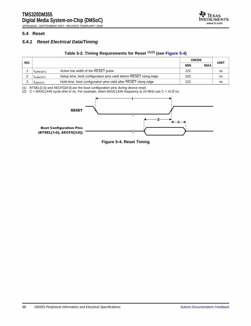
www.ti.com
5.4 Reset
5.4.1 Reset Electrical Data/Timing
1
23
RESET
Boot Configuration Pins
(BTSEL[1:0], AECFG[3:0])
TMS320DM355Digital Media System-on-Chip (DMSoC)SPRS463D–SEPTEMBER 2007–REVISED FEBRUARY 2008
Table 5-2. Timing Requirements for Reset (1) (2) (see Figure 5-4)DM355
NO. UNITMIN MAX
1 tw(RESET) Active low width of the RESET pulse 12C ns2 tsu(BOOT) Setup time, boot configuration pins valid before RESET rising edge 12C ns3 th(BOOT) Hold time, boot configuration pins valid after RESET rising edge 12C ns
(1) BTSEL[1:0] and AECFG[4:0] are the boot configuration pins during device reset.(2) C = MXI/CLKIN cycle time in ns. For example, when MXI/CLKIN frequency is 24 MHz use C = 41.6 ns.
Figure 5-4. Reset Timing
DM355 Peripheral Information and Electrical Specifications98 Submit Documentation Feedback

www.ti.com
5.5 Oscillators and Clocks
5.5.1 MXI1 (24-MHz) Oscillator
Crystal24 MHz or36 MHz
C1 C2
MXI1/CLKIN MXO1 VSS_MX1
0.1 F
1 F
L1
VDDA_PLL1 VSSA_PLL1
CL
C1C2
(C1 C2)
TMS320DM355Digital Media System-on-Chip (DMSoC)SPRS463D–SEPTEMBER 2007–REVISED FEBRUARY 2008
DM355 has two oscillator input/output pairs (MXI1/MXO1 and MXI2/MXO2) usable with external crystalsor ceramic resonators to provide clock inputs. The optimal frequencies for the crystals are 24 MHz(MXI1/MXO1) and 27 MHz (MXI2/MXO2). Optionally, the oscillator inputs are configurable for use withexternal clock oscillators. If external clock oscillators are used, to minimize the clock jitter, a single cleanpower supply should power both the DM355 and the external oscillator circuit and the minimum CLKINrise and fall times must be observed. The electrical requirements and characteristics are described in thissection.
The timing parameters for CLKOUT[3:1] are also described in this section. The DM355 has three outputclock pins (CLKOUT[3:1]). See Section 3.5 and Section 3.6 for more information on CLKOUT[3:1].
The MXI1 (typically 24 MHz, can also be 36 MHz) oscillator provides the primary reference clock for theDM355 device. The on-chip oscillator requires an external crystal connected across the MXI1 and MXO1pins, along with two load capacitors, as shown in Figure 5-5. The external crystal load capacitors must beconnected only to the oscillator ground pin (VSS_MX1). Do not connect to board ground (VSS). Also, the PLLpower pin (VDDA_PLL1) should be connected to the power supply through a ferrite bead, L1 in the examplecircuit shown in Figure 5-5.
Figure 5-5. MXI1 (24-MHz) Oscillator
The load capacitors, C1 and C2, should be chosen such that the equation is satisfied (typical values areC1 = C2 = 10 pF). CL in the equation is the load specified by the crystal manufacturer. All discretecomponents used to implement the oscillator circuit should be placed as close as possible to theassociated oscillator pins (MXI1 and MXO1) and to the VSS_MX1 pin.
Submit Documentation Feedback DM355 Peripheral Information and Electrical Specifications 99

www.ti.com
5.5.2 MXI2 (27-MHz) Oscillator (optional oscillator)
Crystal
27 MHz
C1 C2
MXI2 MXO2 VSS_MX2
L1
VDDA_PLL2 VSSA_PLL2
0.1 F
1 F
CL
C1C2
(C1 C2)
TMS320DM355Digital Media System-on-Chip (DMSoC)SPRS463D–SEPTEMBER 2007–REVISED FEBRUARY 2008
Table 5-3. Switching Characteristics Over Recommended Operating Conditions for 24-MHz SystemOscillator
PARAMETER MIN TYP MAX UNITStart-up time (from power up until oscillating at stable frequency) 4 msOscillation frequency 24 or 36 MHzESR 60 Ω
Frequency stability +/-50 ppm
The MXI2 (27 MHz) oscillator provides an optional reference clock for the DM355's VPSS module. Theon-chip oscillator requires an external 27-MHz crystal connected across the MXI2 and MXO2 pins, alongwith two load capacitors, as shown in Figure 5-6. The external crystal load capacitors must be connectedonly to the 27-MHz oscillator ground pin (VSS_MX2). Do not connect to board ground (VSS). Also, the PLLpower pin (VDDA_PLL2) should be connected to the power supply through a ferrite bead, L1 in the examplecircuit shown in Figure 5-6.
Figure 5-6. MXI2 (27-MHz) System Oscillator
The load capacitors, C1 and C2, should be chosen such that the equation is satisfied (typical values areC1 = C2 = 10 pF). CL in the equation is the load specified by the crystal manufacturer. All discretecomponents used to implement the oscillator circuit should be placed as close as possible to theassociated oscillator pins (MXI and MXO) and to the VSS_MX2 pin.
Table 5-4. Switching Characteristics Over Recommended Operating Conditions for 27-MHz SystemOscillator
PARAMETER MIN TYP MAX UNITStart-up time (from power up until oscillating at stable frequency) 4 msOscillation frequency 27 MHzESR 60 Ω
Frequency stability +/-50 ppm
DM355 Peripheral Information and Electrical Specifications100 Submit Documentation Feedback

www.ti.com
5.5.3 Clock PLL Electrical Data/Timing (Input and Output Clocks)
MXI/CLKIN
2
3
4
4
5 1
MXI/CLKIN
2
3
4
4
5 1
TMS320DM355Digital Media System-on-Chip (DMSoC)SPRS463D–SEPTEMBER 2007–REVISED FEBRUARY 2008
Table 5-5. Timing Requirements for MXI1/CLKIN1 (1) (2) (see Figure 5-7)DM355NO UNIT. MIN TYP MAX
1 tc(MXI1) Cycle time, MXI1/CLKIN1 27.7 (3) 41.6 (3) ns2 tw(MXI1H) Pulse duration, MXI1/CLKIN1 high 0.45C 0.55C ns3 tw(MXI1L) Pulse duration, MXI1/CLKIN1 low 0.45C 0.55C ns4 tt(MXI1) Transition time, MXI1/CLKIN1 0.05C ns5 tJ(MXI1) Period jitter, MXI1/CLKIN1 0.02C ns
(1) The reference points for the rise and fall transitions are measured at VIL MAX and VIH MIN.(2) C = MXI1/CLKIN1 cycle time in ns. For example, when MXI1/CLKIN1 frequency is 24 MHz use C = 41.6 ns.(3) tc(MXI1) = 41.6 ns and tc(MXI1) = 27.7 ns are the only supported cycle times for MXI1/CLKIN1.
Figure 5-7. MXI1/CLKIN1 Timing
Table 5-6. Timing Requirements for MXI2/CLKIN2 (1) (2) (see Figure 5-7)NO. DM355 UNIT
MIN TYP MAX1 tc(MXI2) Cycle time, MXI2/CLKIN2 37.037 (3) 37.037 (3) ns2 tw(MXI2H) Pulse duration, MXI2/CLKIN2 high 0.45C 0.55C ns3 tw(MXI2L) Pulse duration, MXI2/CLKIN2 low 0.45C 0.55C ns4 tt(MXI2) Transition time, MXI2/CLKIN2 0.05C ns5 tJ(MXI2) Period jitter, MXI2/CLKIN2 0.02C ns
(1) The reference points for the rise and fall transitions are measured at VIL MAX and VIH MIN.(2) C = MXI2/CLKIN2 cycle time in ns. For example, when MXI2/CLKIN2 frequency is 27 MHz use C = 37.037 ns.(3) tc(MXI2) = 37.037 ns is the only supported cycle time for MXI2/CLKIN2.
Figure 5-8. MXI2/CLKIN2 Timing
Submit Documentation Feedback DM355 Peripheral Information and Electrical Specifications 101
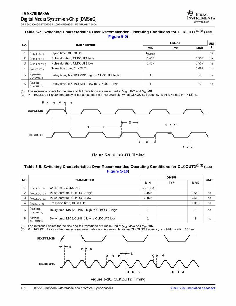
www.ti.com
CLKOUT1
1
24
4
MXI/CLKIN
5 6
3
MXI/CLKIN
CLKOUT2
12
3
4
56
4
TMS320DM355Digital Media System-on-Chip (DMSoC)SPRS463D–SEPTEMBER 2007–REVISED FEBRUARY 2008
Table 5-7. Switching Characteristics Over Recommended Operating Conditions for CLKOUT1 (1) (2) (seeFigure 5-9)
DM355 UNINO. PARAMETER TMIN TYP MAX1 tC(CLKOUT1) Cycle time, CLKOUT1 tc(MXI1) ns2 tw(CLKOUT1H) Pulse duration, CLKOUT1 high 0.45P 0.55P ns3 tw(CLKOUT1L) Pulse duration, CLKOUT1 low 0.45P 0.55P ns4 tt(CLKOUT1) Transition time, CLKOUT1 0.05P ns
td(MXI1H-5 Delay time, MXI1/CLKIN1 high to CLKOUT1 high 1 8 nsCLKOUT1H)
td(MXI1L-6 Delay time, MXI1/CLKIN1I low to CLKOUT1 low 1 8 nsCLKOUT1L)
(1) The reference points for the rise and fall transitions are measured at VOL MAX and VOHMIN.(2) P = 1/CLKOUT1 clock frequency in nanoseconds (ns). For example, when CLKOUT1 frequency is 24 MHz use P = 41.6 ns.
Figure 5-9. CLKOUT1 Timing
Table 5-8. Switching Characteristics Over Recommended Operating Conditions for CLKOUT2 (1) (2) (seeFigure 5-10)
DM355NO. PARAMETER UNIT
MIN TYP MAX1 tC(CLKOUT2) Cycle time, CLKOUT2 tc(MXI1) /32 tw(CLKOUT2H) Pulse duration, CLKOUT2 high 0.45P 0.55P ns3 tw(CLKOUT2L) Pulse duration, CLKOUT2 low 0.45P 0.55P ns4 tt(CLKOUT2) Transition time, CLKOUT2 0.05P ns
td(MXI1H-5 Delay time, MXI1/CLKIN1 high to CLKOUT2 high 1 8 nsCLKOUT2H)
td(MXI1L-6 Delay time, MXI1/CLKIN1 low to CLKOUT2 low 1 8 nsCLKOUT2L)
(1) The reference points for the rise and fall transitions are measured at VOL MAX and VOHMIN.(2) P = 1/CLKOUT2 clock frequency in nanoseconds (ns). For example, when CLKOUT2 frequency is 8 MHz use P = 125 ns.
Figure 5-10. CLKOUT2 Timing
DM355 Peripheral Information and Electrical Specifications102 Submit Documentation Feedback

www.ti.com
5 6
1
2 3
4
4
MXI/CLKIN
CLKOUT3
TMS320DM355Digital Media System-on-Chip (DMSoC)SPRS463D–SEPTEMBER 2007–REVISED FEBRUARY 2008
Table 5-9. Switching Characteristics Over Recommended Operating Conditions for CLKOUT3 (1) (2) (seeFigure 5-11)
DM355NO. PARAMETER UNIT
MIN TYP MAX1 tC(CLKOUT3) Cycle time, CLKOUT3 tc(MXI1) /82 tw(CLKOUT3H) Pulse duration, CLKOUT3 high 0.45P 0.55P ns3 tw(CLKOUT3L) Pulse duration, CLKOUT3 low 0.45P 0.55P ns4 tt(CLKOUT3) Transition time, CLKOUT3 0.05P ns
td(MXI2H-5 Delay time, CLKIN/MXI high to CLKOUT3 high 1 8 nsCLKOUT3H)
td(MXI2L-6 Delay time, CLKIN/MXI low to CLKOUT3 low 1 8 nsCLKOUT3L)
(1) The reference points for the rise and fall transitions are measured at VOL MAX and VOHMIN.(2) P = 1/CLKOUT3 clock frequency in nanoseconds (ns). For example, when CLKOUT3 frequency is 3 MHz use P = 333.3 ns.
Figure 5-11. CLKOUT3 Timing
Submit Documentation Feedback DM355 Peripheral Information and Electrical Specifications 103

www.ti.com
5.6 General-Purpose Input/Output (GPIO)
5.6.1 GPIO Peripheral Input/Output Electrical Data/Timing
TMS320DM355Digital Media System-on-Chip (DMSoC)SPRS463D–SEPTEMBER 2007–REVISED FEBRUARY 2008
The GPIO peripheral provides general-purpose pins that can be configured as either inputs or outputs.When configured as an output, a write to an internal register can control the state driven on the output pin.When configured as an input, the state of the input is detectable by reading the state of an internalregister. In addition, the GPIO peripheral can produce CPU interrupts and EDMA events in differentinterrupt/event generation modes. The GPIO peripheral provides generic connections to external devices.The GPIO pins are grouped into banks of 16 pins per bank (i.e., bank 0 consists of GPIO [0:15]). Thereare a total of 7 GPIO banks in the DM355, because the DM355 has 104 GPIOs.
The DM355 GPIO peripheral supports the following:• Up to 104 3.3v GPIO pins, GPIO[103:0]• Interrupts:
– Up to 10 unique GPIO[9:0] interrupts from Bank 0– Up to 7 GPIO (bank aggregated) interrupt signals, one from each of the 7 banks of GPIOs– Interrupts can be triggered by rising and/or falling edge, specified for each interrupt capable GPIO
signal• DMA events:
– Up to 10 unique GPIO DMA events from Bank 0– Up to 7 GPIO (bank aggregated) DMA event signals, one from each of the 7 banks of GPIOs
• Set/clear functionality: Firmware writes 1 to corresponding bit position(s) to set or to clear GPIOsignal(s). This allows multiple firmware processes to toggle GPIO output signals without critical sectionprotection (disable interrupts, program GPIO, re-enable interrupts, to prevent context switching toanther process during GPIO programming).
• Separate Input/Output registers• Output register in addition to set/clear so that, if preferred by firmware, some GPIO output signals can
be toggled by direct write to the output register(s).• Output register, when read, reflects output drive status. This, in addition to the input register reflecting
pin status and open-drain I/O cell, allows wired logic be implemented.
For more detailed information on GPIOs, see the Documentation Support section for the General-PurposeInput/Output (GPIO) Reference Guide.
Table 5-10. Timing Requirements for GPIO Inputs (see Figure 5-12)DM355
NO. UNITMIN MAX
1 tw(GPIH) Pulse duration, GPIx high 52 ns2 tw(GPIL) Pulse duration, GPIx low 52 ns
Table 5-11. Switching Characteristics Over Recommended Operating Conditions for GPIO Outputs(see Figure 5-12)
DM355NO. PARAMETER UNIT
MIN MAX3 tw(GPOH) Pulse duration, GPOx high 26 (1) ns4 tw(GPOL) Pulse duration, GPOx low 26 (1) ns
(1) This parameter value should not be used as a maximum performance specification. Actual performance of back-to-back accesses of theGPIO is dependent upon internal bus activity.
DM355 Peripheral Information and Electrical Specifications104 Submit Documentation Feedback

www.ti.com
GPIx
GPOx
4
3
2
1
5.6.2 GPIO Peripheral External Interrupts Electrical Data/Timing
EXT_INTx
2
1
TMS320DM355Digital Media System-on-Chip (DMSoC)SPRS463D–SEPTEMBER 2007–REVISED FEBRUARY 2008
Figure 5-12. GPIO Port Timing
Table 5-12. Timing Requirements for External Interrupts/EDMA Events (1) (see Figure 5-13)DM355
NO. UNITMIN MAX
1 tw(ILOW) Width of the external interrupt pulse low 52 ns2 tw(IHIGH) Width of the external interrupt pulse high 52 ns
(1) The pulse width given is sufficient to generate an interrupt or an EDMA event. However, if a user wants to have DM355 to recognize theGPIO changes through software polling of the GPIO register, the GPIO duration must be extended to allow DM355 enough time toaccess the GPIO register through the internal bus.
Figure 5-13. GPIO External Interrupt Timing
Submit Documentation Feedback DM355 Peripheral Information and Electrical Specifications 105

www.ti.com
5.7 External Memory Interface (EMIF)
5.7.1 Asynchronous EMIF (AEMIF)
5.7.1.1 NAND (NAND, SmartMedia, xD)
5.7.1.2 OneNAND
TMS320DM355Digital Media System-on-Chip (DMSoC)SPRS463D–SEPTEMBER 2007–REVISED FEBRUARY 2008
DM355 supports several memory and external device interfaces, including:• Asynchronous EMIF (AEMIF) for interfacing to SRAM.
– OneNAND flash memories– NAND flash memories
• DDR2/mDDR Memory Controller for interfacing to SDRAM.
The EMIF supports the following features:• SRAM, etc. on up to 2 asynchronous chip selects addressable up to 64KB each• Supports 8-bit or 16-bit data bus widths• Programmable asynchronous cycle timings• Supports extended wait mode• Supports Select Strobe mode
The NAND features of the EMIF are as follows:• NAND flash on up to 2 asynchronous chip selects• 8 and 16-bit data bus widths• Programmable cycle timings• Performs 1-bit and 4-bit ECC calculation• NAND Mode also supports SmartMedia/SSFDC (Solid State Floppy Disk Controller) and xD memory
cards
The OneNAND features supported are as follows.• NAND flash on up to 2 asynchronous chip selects• Only 16-bit data bus widths• Supports asynchronous writes and reads• Supports synchronous reads with continuous linear burst mode (Does not support synchronous reads
with wrap burst modes)• Programmable cycle timings for each chip select in asynchronous mode
DM355 Peripheral Information and Electrical Specifications106 Submit Documentation Feedback

www.ti.com
5.7.1.3 AEMIF Electrical Data/Timing
TMS320DM355Digital Media System-on-Chip (DMSoC)SPRS463D–SEPTEMBER 2007–REVISED FEBRUARY 2008
Table 5-13. Timing Requirements for Asynchronous Memory Cycles for AEMIF Module (1) (see Figure 5-14and Figure 5-15)
DM355NO UNIT. MIN Nom MAXREADS and WRITES
Pulse duration, EM_WAIT assertion and2 tw(EM_WAIT) 2E nsdeassertionREADS
12 tsu(EMDV-EMOEH) Setup time, EM_D[15:0] valid before EM_OE high 5 ns13 th(EMOEH-EMDIV) Hold time, EM_D[15:0] valid after EM_OE high 0 ns
tsu(EMOEL- Delay time from EM_OE low to EM_WAIT14 4E nsEMWAIT) asserted (2)
READS (OneNAND Synchronous Burst Read)Setup time, EM_D[15:0] valid before EM_CLK30 tsu(EMDV-EMCLKH) 4 nshigh
31 th(EMCLKH-EMDIV) Hold time, EM_D[15:0] valid after EM_CLK high 4 nsWRITES
tsu(EMWEL- Delay time from EM_WE low to EM_WAIT28 4E nsEMWAIT) asserted (2)
(1) E = PLLC1 SYSCLK2 period in ns. SYSCLK2 is the EMIF peripheral clock. SYSCLK2 is one-fourth the PLLC output clock. For example,when PLLC output clock = 432 MHz, E = 9.259 ns. See Section 3.5 for more information.
(2) Setup before end of STROBE phase (if no extended wait states are inserted) by which EM_WAIT must be asserted to add extendedwait states. Figure 5-16 and Figure 5-17 describe EMIF transactions that include extended wait states inserted during the STROBEphase. However, cycles inserted as part of this extended wait period should not be counted; the 4E requirement is to the start of wherethe HOLD phase would begin if there were no extended wait cycles.
Table 5-14. Switching Characteristics Over Recommended Operating Conditions for AsynchronousMemory Cycles for AEMIF Module (1) (2) (3) (see Figure 5-14 and Figure 5-15)
DM355 UNINO. PARAMETER TMIN Nom MAXREADS and WRITES
1 td(TURNAROUND) Turn around time (TA)*E nsREADS
EMIF read cycle time (EW = 0) (RS+RST+RH)*E ns3 tc(EMRCYCLE) (RS+RST+RH+(EWC*EMIF read cycle time (EW = 1) ns16))*E
Output setup time, EM_CE[1:0] low to (RS)*E nsEM_OE low (SS = 0)4 tsu(EMCEL-EMOEL) Output setup time, EM_CE[1:0] low to 0 nsEM_OE low (SS = 1)
Output hold time, EM_OE high to (RH)*E nsEM_CE[1:0] high (SS = 0)5 th(EMOEH-EMCEH) Output hold time, EM_OE high to 0 nsEM_CE[1:0] high (SS = 1)
(1) TA = Turn around, RS = Read setup, RST = Read strobe, RH = Read hold, WS = Write setup, WST = Write strobe, WH = Write hold,MEWC = Maximum external wait cycles. These parameters are programmed via the Asynchronous Bank and Asynchronous Wait CycleConfiguration Registers. These support the following range of values: TA[4-1], RS[16-1], RST[64-1], RH[8-1], WS[16-1], WST[64-1],WH[8-1], and MEW[1-256]. See the TMS320DM355 DMSoC Asynchronous External Memory Interface (EMIF) User's Guide (SPRUED1)for more information.
(2) E = PLLC1 SYSCLK2 period in ns. SYSCLK2 is the EMIF peripheral clock. SYSCLK2 is one-fourth the PLLC output clock. For example,when PLLC output clock = 432 MHz, E = 9.259 ns. See Section 3.5 for more information
(3) EWC = external wait cycles determined by EM_WAIT input signal. EWC supports the following range of values EWC[256-1]. Note thatthe maximum wait time before timeout is specified by bit field MEWC in the Asynchronous Wait Cycle Configuration Register. See theTMS320DM355 DMSoC Asynchronous External Memory Interface (EMIF) User's Guide (SPRUED1) for more information.
Submit Documentation Feedback DM355 Peripheral Information and Electrical Specifications 107
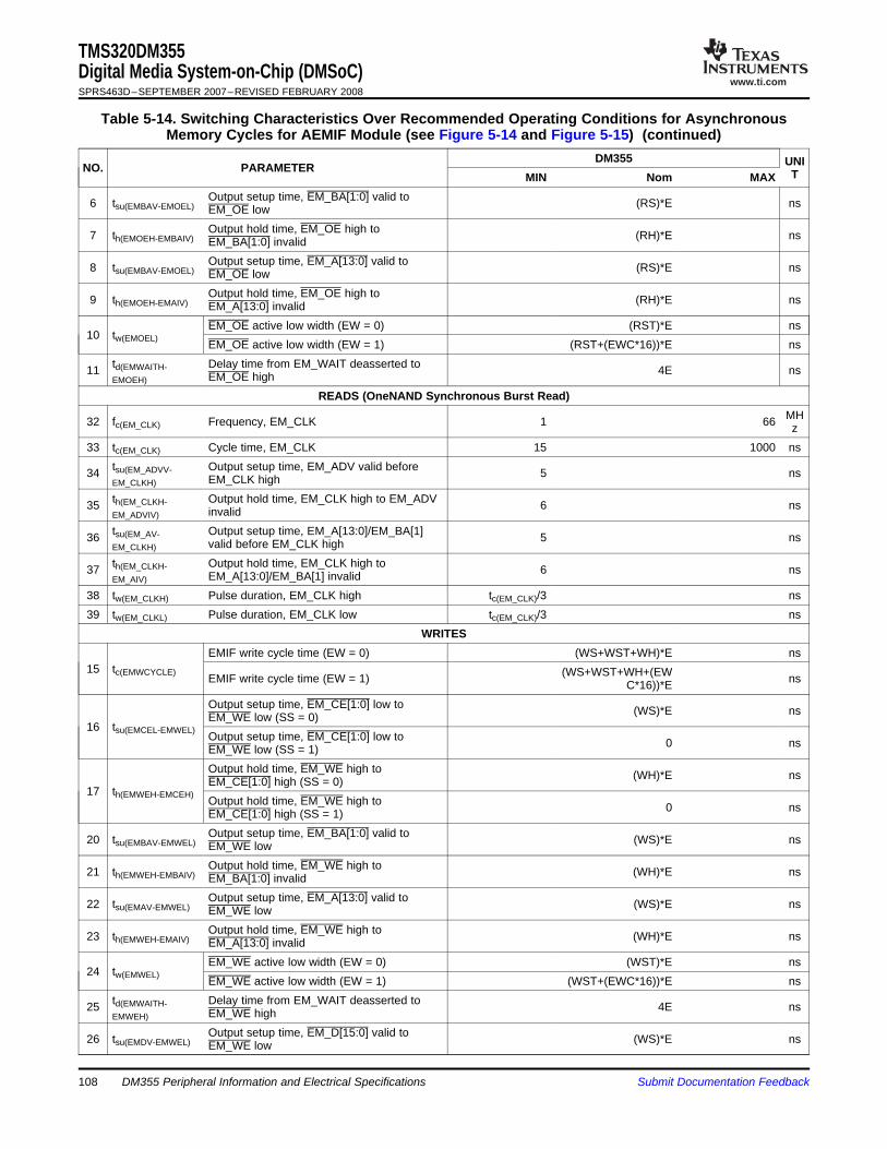
www.ti.com
TMS320DM355Digital Media System-on-Chip (DMSoC)SPRS463D–SEPTEMBER 2007–REVISED FEBRUARY 2008
Table 5-14. Switching Characteristics Over Recommended Operating Conditions for AsynchronousMemory Cycles for AEMIF Module (see Figure 5-14 and Figure 5-15) (continued)
DM355 UNINO. PARAMETER TMIN Nom MAXOutput setup time, EM_BA[1:0] valid to6 tsu(EMBAV-EMOEL) (RS)*E nsEM_OE lowOutput hold time, EM_OE high to7 th(EMOEH-EMBAIV) (RH)*E nsEM_BA[1:0] invalidOutput setup time, EM_A[13:0] valid to8 tsu(EMBAV-EMOEL) (RS)*E nsEM_OE lowOutput hold time, EM_OE high to9 th(EMOEH-EMAIV) (RH)*E nsEM_A[13:0] invalidEM_OE active low width (EW = 0) (RST)*E ns
10 tw(EMOEL) EM_OE active low width (EW = 1) (RST+(EWC*16))*E nstd(EMWAITH- Delay time from EM_WAIT deasserted to11 4E nsEMOEH) EM_OE high
READS (OneNAND Synchronous Burst Read)MH32 fc(EM_CLK) Frequency, EM_CLK 1 66 z
33 tc(EM_CLK) Cycle time, EM_CLK 15 1000 nstsu(EM_ADVV- Output setup time, EM_ADV valid before34 5 nsEM_CLKH) EM_CLK highth(EM_CLKH- Output hold time, EM_CLK high to EM_ADV35 6 nsEM_ADVIV) invalidtsu(EM_AV- Output setup time, EM_A[13:0]/EM_BA[1]36 5 nsEM_CLKH) valid before EM_CLK highth(EM_CLKH- Output hold time, EM_CLK high to37 6 nsEM_AIV) EM_A[13:0]/EM_BA[1] invalid
38 tw(EM_CLKH) Pulse duration, EM_CLK high tc(EM_CLK)/3 ns39 tw(EM_CLKL) Pulse duration, EM_CLK low tc(EM_CLK)/3 ns
WRITESEMIF write cycle time (EW = 0) (WS+WST+WH)*E ns
15 tc(EMWCYCLE) (WS+WST+WH+(EWEMIF write cycle time (EW = 1) nsC*16))*EOutput setup time, EM_CE[1:0] low to (WS)*E nsEM_WE low (SS = 0)
16 tsu(EMCEL-EMWEL) Output setup time, EM_CE[1:0] low to 0 nsEM_WE low (SS = 1)Output hold time, EM_WE high to (WH)*E nsEM_CE[1:0] high (SS = 0)
17 th(EMWEH-EMCEH) Output hold time, EM_WE high to 0 nsEM_CE[1:0] high (SS = 1)Output setup time, EM_BA[1:0] valid to20 tsu(EMBAV-EMWEL) (WS)*E nsEM_WE lowOutput hold time, EM_WE high to21 th(EMWEH-EMBAIV) (WH)*E nsEM_BA[1:0] invalidOutput setup time, EM_A[13:0] valid to22 tsu(EMAV-EMWEL) (WS)*E nsEM_WE lowOutput hold time, EM_WE high to23 th(EMWEH-EMAIV) (WH)*E nsEM_A[13:0] invalidEM_WE active low width (EW = 0) (WST)*E ns
24 tw(EMWEL) EM_WE active low width (EW = 1) (WST+(EWC*16))*E nstd(EMWAITH- Delay time from EM_WAIT deasserted to25 4E nsEMWEH) EM_WE high
Output setup time, EM_D[15:0] valid to26 tsu(EMDV-EMWEL) (WS)*E nsEM_WE low
DM355 Peripheral Information and Electrical Specifications108 Submit Documentation Feedback
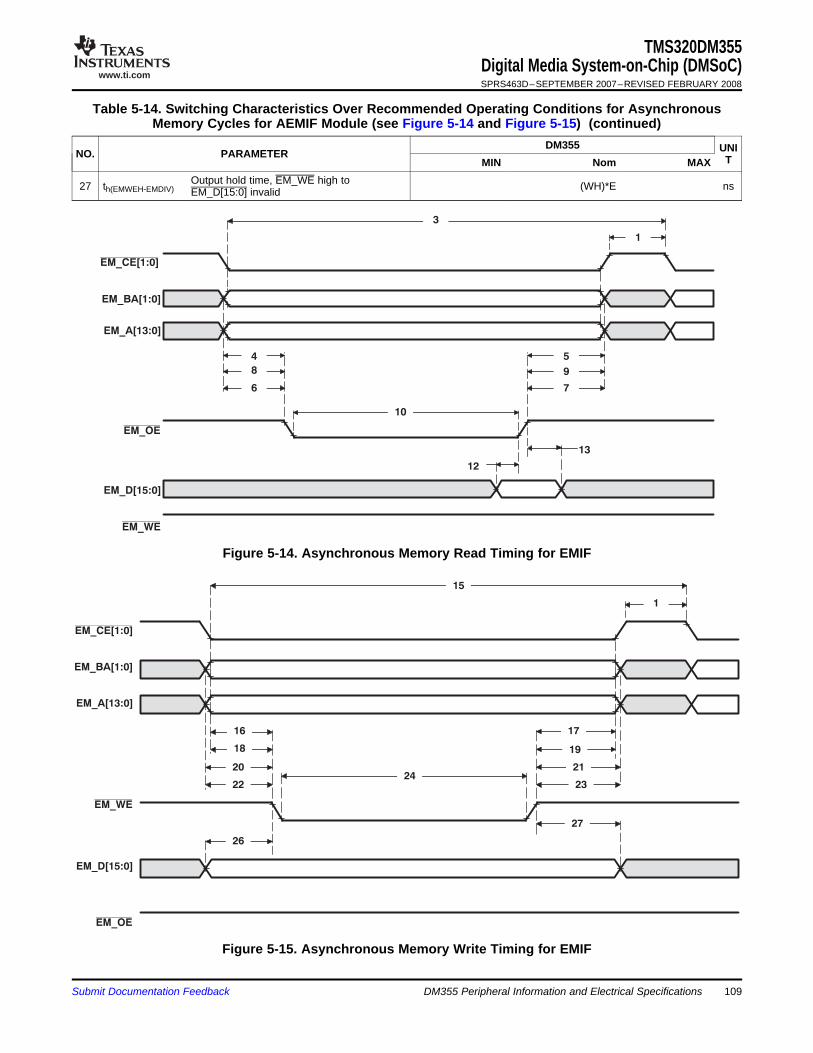
www.ti.com
EM_CE[1:0]
EM_BA[1:0]
13
12
EM_A[13:0]
EM_OE
EM_D[15:0]
EM_WE
10
5
9
7
4
8
6
3
1
EM_CE[1:0]
EM_BA[1:0]
EM_A[13:0]
EM_WE
EM_D[15:0]
EM_OE
15
1
16
18
20
2224
17
19
21
23
26
27
TMS320DM355Digital Media System-on-Chip (DMSoC)SPRS463D–SEPTEMBER 2007–REVISED FEBRUARY 2008
Table 5-14. Switching Characteristics Over Recommended Operating Conditions for AsynchronousMemory Cycles for AEMIF Module (see Figure 5-14 and Figure 5-15) (continued)
DM355 UNINO. PARAMETER TMIN Nom MAXOutput hold time, EM_WE high to27 th(EMWEH-EMDIV) (WH)*E nsEM_D[15:0] invalid
Figure 5-14. Asynchronous Memory Read Timing for EMIF
Figure 5-15. Asynchronous Memory Write Timing for EMIF
Submit Documentation Feedback DM355 Peripheral Information and Electrical Specifications 109

www.ti.com
EM_CE[1:0]
11
Asserted Deasserted
22
14
EM_BA[1:0]
EM_A[13:0]
EM_D[15:0]
EM_OE
EM_WAIT
SETUP STROBE Extended Due to EM_WAIT STROBE HOLD
EM_CE[1:0]
25
Asserted Deasserted
22
EM_BA[1:0]
EM_A[13:0]
EM_D[15:0]
EM_WE
EM_WAIT
SETUP STROBE Extended Due to EM_WAIT STROBE HOLD
28
TMS320DM355Digital Media System-on-Chip (DMSoC)SPRS463D–SEPTEMBER 2007–REVISED FEBRUARY 2008
Figure 5-16. EM_WAIT Read Timing Requirements
Figure 5-17. EM_WAIT Write Timing Requirements
DM355 Peripheral Information and Electrical Specifications110 Submit Documentation Feedback

www.ti.com
34
33
35
36
37 30
31
Da Da+1 Da+2 Da+3 Da+4 Da+5 Da+n
Da+n+1
EM_CLK
EM_CE[1:0]
EM_ADV
EM_BA0,EM_A[13:0],
EM_BA1
EM_D[15:0]
EM_OE
EM_WAIT
38
39
TMS320DM355Digital Media System-on-Chip (DMSoC)SPRS463D–SEPTEMBER 2007–REVISED FEBRUARY 2008
Figure 5-18. Synchronous OneNAND Flash Read Timing
Submit Documentation Feedback DM355 Peripheral Information and Electrical Specifications 111
www.ti.com
5.7.2 DDR2/mDDR Memory Controller
5.7.2.1 DDR2/mDDR Memory Controller Electrical Data/Timing
TMS320DM355Digital Media System-on-Chip (DMSoC)SPRS463D–SEPTEMBER 2007–REVISED FEBRUARY 2008
The DDR2 / mDDR Memory Controller is a dedicated interface to DDR2 / mDDR SDRAM. It supportsJESD79D-2A standard compliant DDR2 SDRAM devices and compliant Mobile DDR SDRAM devices.DDR2 / mDDR SDRAM plays a key role in a DM355-based system. Such a system is expected to requirea significant amount of high-speed external memory for all of the following functions:• Buffering of input image data from sensors or video sources• Intermediate buffering for processing/resizing of image data in the VPFE• Numerous OSD display buffers• Intermediate buffering for large raw Bayer data image files while performing image processing
functions• Buffering for intermediate data while performing video encode and decode functions• Storage of executable code for the ARM
The DDR2 / mDDR Memory Controller supports the following features:• JESD79D-2A standard compliant DDR2 SDRAM• Mobile DDR SDRAM• 256 MByte memory space• Data bus width 16 bits• CAS latencies:
– DDR2: 2, 3, 4, and 5– mDDR: 2 and 3
• Internal banks:– DDR2: 1, 2, 4, and 8– mDDR: 1, 2, and 4
• Burst length: 8
• Burst type: sequential
• 1 CS signal• Page sizes: 256, 512, 1024, and 2048• SDRAM autoinitialization• Self-refresh mode• Partial array self-refresh (for mDDR)• Power down mode• Prioritized refresh• Programmable refresh rate and backlog counter• Programmable timing parameters• Little endian
For details on the DDR2 Memory Controller, refer to TMS320DM35x Digital Media System-on-Chip(DMSoC) DDR2/mDDR Memory Controller Reference Guide (literature number SPRUEH7).
The Implementing DDR2/mDDR PCB Layout on the TMS320DM35x DMSoC Application Report (literaturenumber SPRAAR3) specifies a complete DDR2 and mDDR interface solution for the DM355 as well as alist of compatible DDR2/mDDR devices. TI has performed the simulation and system characterization toensure all DDR2 and mDDR interface timings in this solution are met.
TI only supports board designs that follow the guidelines outlined in the Implementing DDR2/mDDR PCBLayout on the TMS320DM35x DMSoC Application Report (literature number SPRAAR3).
DM355 Peripheral Information and Electrical Specifications112 Submit Documentation Feedback

www.ti.com
5.8 MMC/SD
5.8.1 MMC/SD Electrical Data/Timing
TMS320DM355Digital Media System-on-Chip (DMSoC)SPRS463D–SEPTEMBER 2007–REVISED FEBRUARY 2008
The DM355 includes two separate MMC/SD Controllers which are compliant with MMC V3.31, SecureDigital Part 1 Physical Layer Specification V1.1 and Secure Digital Input Output (SDIO) V1.0specifications.
The DM355 MMC/SD Controller has following features:• MultiMediaCard (MMC).• Secure Digital (SD) Memory Card.• MMC/SD protocol support.• SDIO protocol support.• Programmable clock frequency.• 256 bit Read/Write FIFO to lower system overhead.• Slave EDMA transfer capability.
The DM355 MMC/SD Controller does not support SPI mode.
Table 5-15. Timing Requirements for MMC/SD Module(see Figure 5-20 and Figure 5-22)
DM355NO. FAST MODE STANDARD MODE UNIT
MIN MAX MIN MAX1 tsu(CMDV-CLKH) Setup time, SD_CMD valid before SD_CLK high 6 5 ns2 th(CLKH-CMDV) Hold time, SD_CMD valid after SD_CLK high 2.5 (1) 5 ns3 tsu(DATV-CLKH) Setup time, SD_DATx valid before SD_CLK high 6 5 ns4 th(CLKH-DATV) Hold time, SD_DATx valid after SD_CLK high 2.5 5 ns
(1) For this parameter, you may include margin in your board design so that the toh = 2.5 ns of the MMC/SD device is not degraded at theDM355 input pin.
Table 5-16. Switching Characteristics Over Recommended Operating Conditions for MMC/SD Module(see Figure 5-19 through Figure 5-22)
DM355STANDARDNO. PARAMETER FAST MODE UNITMODE
MIN MAX MIN MAX7 f(CLK) Operating frequency, SD_CLK 0 50 0 25 MHz8 f(CLK_ID) Identification mode frequency, SD_CLK 0 400 0 400 KHz9 tW(CLKL) Pulse width, SD_CLK low 7 10 ns
10 tW(CLKH) Pulse width, SD_CLK high 7 10 ns11 tr(CLK) Rise time, SD_CLK 3 10 ns12 tf(CLK) Fall time, SD_CLK 3 10 ns
td(CLKL-13 Delay time, SD_CLK low to SD_CMD transition -7.5 4 -7.5 14 nsCMD)
14 td(CLKL-DAT) Delay time, SD_CLK low to SD_DATx transition -7.5 4 -7.5 14 ns
Submit Documentation Feedback DM355 Peripheral Information and Electrical Specifications 113
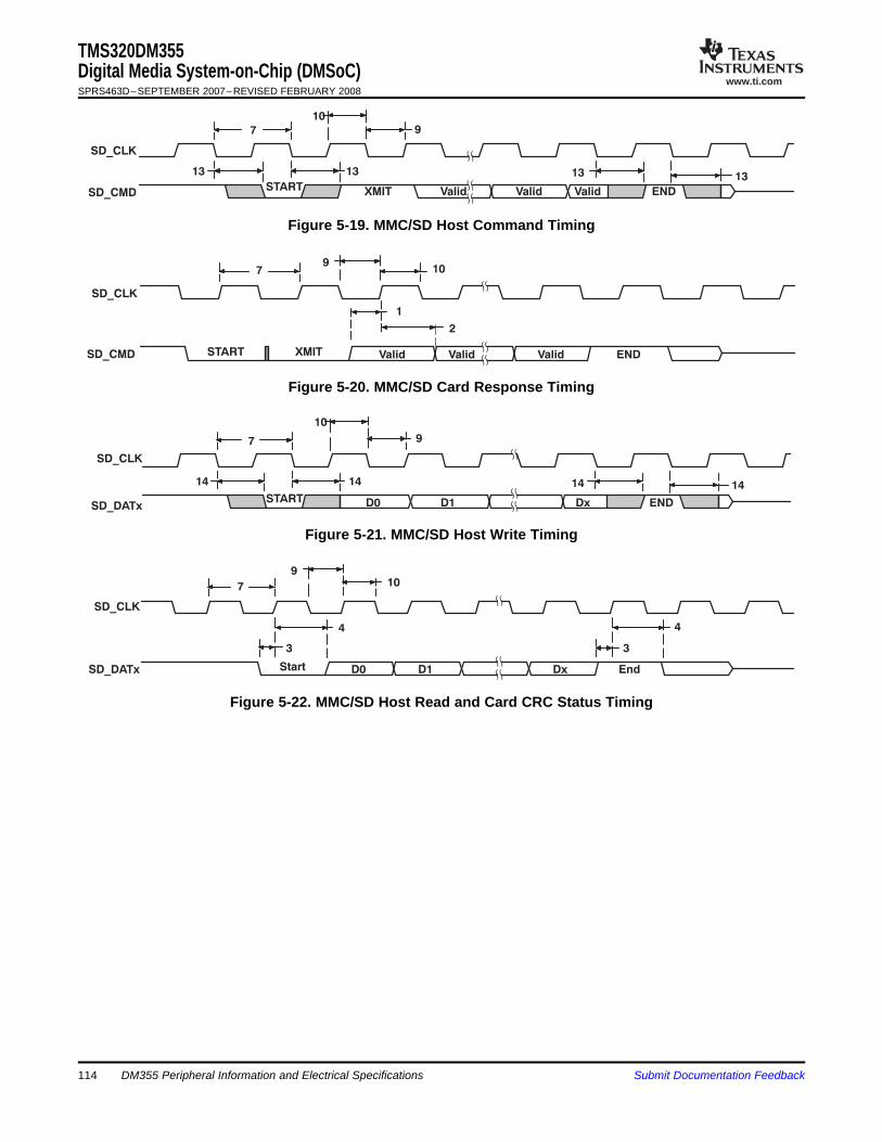
www.ti.com
START XMIT Valid Valid Valid END
SD_CLK
SD_CMD
13
7
109
13 13 13
START XMIT Valid Valid Valid END
SD_CLK
SD_CMD
109
7
1
2
START D0 D1 Dx END
SD_CLK
SD_DATx
7
1414
10
9
14 14
Start D0 D1 Dx End
7
SD_CLK
SD_DATx
910
4
3 3
4
TMS320DM355Digital Media System-on-Chip (DMSoC)SPRS463D–SEPTEMBER 2007–REVISED FEBRUARY 2008
Figure 5-19. MMC/SD Host Command Timing
Figure 5-20. MMC/SD Card Response Timing
Figure 5-21. MMC/SD Host Write Timing
Figure 5-22. MMC/SD Host Read and Card CRC Status Timing
DM355 Peripheral Information and Electrical Specifications114 Submit Documentation Feedback

www.ti.com
5.9 Video Processing Sub-System (VPSS) Overview
5.9.1 Video Processing Front-End (VPFE)
5.9.1.1 CCD Controller (CCDC)
TMS320DM355Digital Media System-on-Chip (DMSoC)SPRS463D–SEPTEMBER 2007–REVISED FEBRUARY 2008
The DM355 contains a Video Processing Sub-System (VPSS) that provides an input interface (VideoProcessing Front End or VPFE) for external imaging peripherals such as image sensors, video decoders,etc.; and an output interface (Video Processing Back End or VPBE) for display devices, such as analogSDTV displays, digital LCD panels, HDTV video encoders, etc.
In addition to these peripherals, there is a set of common buffer memory and DMA control to ensureefficient use of the DDR2 burst bandwidth. The shared buffer logic/memory is a unique block that istailored for seamlessly integrating the VPSS into an image/video processing system. It acts as the primarysource or sink to all the VPFE and VPBE modules that are either requesting or transferring data from/toDDR2. In order to efficiently utilize the external DDR2 bandwidth, the shared buffer logic/memoryinterfaces with the DMA system via a high bandwidth bus (64-bit wide). The shared buffer logic/memoryalso interfaces with all the VPFE and VPBE modules via a 128-bit wide bus. The shared bufferlogic/memory (divided into the read & write buffers and arbitration logic) is capable of performing thefollowing functions. It is imperative that the VPSS utilize DDR2 bandwidth efficiently due to both its largebandwidth requirements and the real-time requirements of the VPSS modules. Because it is possible toconfigure the VPSS modules in such a way that DDR2 bandwidth is exceeded, a set of user accessibleregisters is provided to monitor overflows or failures in data transfers.
The VPFE or Video Processing Front-End block is comprised of the CCD Controller (CCDC), Image Pipe(IPIPE), and Hardware 3A Statistic Generator (H3A). These modules are described in the sections thatfollow.
The CCDC is responsible for accepting raw (unprocessed) image/video data from a sensor (CMOS orCCD). In addition, the CCDC can accept YUV video data in numerous formats, typically from so-calledvideo decoder devices. In the case of raw inputs, the CCDC output requires additional image processingto transform the raw input image to the final processed image. This processing can be done eitheron-the-fly in the Preview Engine hardware ISP or in software on the ARM and MPEG4/JPEG coprocessorsubsystems. In parallel, raw data input to the CCDC can also used for computing various statistics (3A,Histogram) to eventually control the image/video tuning parameters. The CCDC is programmed via controland parameter registers. DM355 performance is enhanced by its dedicated hard-wired MPEG4/JPEGcoprocessor (MJCP). The MJCP performs all the computational operations required for JPEG and MPEG4compression. These operations can be invoked using the xDM (xDIAS for Digital Media) APIs. For moreinformation, refer to the xDIAS-DM (xDIAS for Digital Media) User's Guide (SPRUEC8). The followingfeatures are supported by the CCDC module.• Support for conventional Bayer pattern.• Generates HD/VD timing signals and field ID to an external timing generator or can synchronize to the
external timing generator.• Support for progressive and interlaced sensors (hardware support for up to 2 fields and firmware
support for higher number of fields, typically 3-, 4-, and 5-field sensors).• Support for up to 75-MHZ sensor pixel clock if H3A is not used, otherwise the pixel clock must be less
than 67.5 MHZ• Support for ITU-R BT.656 standard format, either 8-bit or 16-bit.• Support for YCbCr 422 format, either 8- or 16-bit with discrete H and VSYNC signals.• Support for up to 14-bit input.• Support for color space conversion• Generates optical black clamping signals.• Support for shutter signal control.• Support for digital clamping and black level compensation.• Fault pixel correction based on a lookup table that contains row and column position of the pixel to be
Submit Documentation Feedback DM355 Peripheral Information and Electrical Specifications 115

www.ti.com
5.9.1.2 IPIPE - Image Pipe
TMS320DM355Digital Media System-on-Chip (DMSoC)SPRS463D–SEPTEMBER 2007–REVISED FEBRUARY 2008
corrected.• Support for program lens shading correction.• Support for 10-bit to 8-bit A-law compression.• Support for a low-pass filter prior to writing to SDRAM. If this filter is enabled, 2 pixels each in the left
and right edges of each line are cropped from the output.• Support for generating output to range from 14-bits to 8-bits wide (8-bits wide allows for 50% saving in
storage area).• Support for down sampling via programmable culling patterns.• Ability to control output to the DDR2 via an external write enable signal.• Support for up to 32K pixels (image size) in both the horizontal and vertical direction.
The hardware Image Pipe (IPIPE) is a programmable hardware image processing module that isresponsible for transforming raw (unprocessed) image/video data from a sensor (CMOS or CCD) intoYCbCr 422 data that is amenable for compression or display. The IPIPE can also be configured to operatein a resize only mode, which allows YCbCr 422 to be resized without applying the processing of everymodule in the IPIPE. Typically, the output of the IPIPE is used for both video compression and displayingit on an external display device such as a NTSC/PAL analog encoder or a digital LCD. The IPIPE isprogrammed via control and parameter registers. The following features are supported by the IPIPE.• The input interface extracts valid raw data from the CCD raw data, and then various modules in IPIPE
process the raw CCD data.• The 2D noise filter module reduces impulse noise in the raw data and adjusts the resolution of the
input image.• The 2D pre-filter adjusts the resolution of the input image and remove line crawl noise.• The white balance module applies two gain adjustments to the data: a digital gain (total gain) and a
white balance gain.• The Color Filter Array (CFA) interpolation module implements CFA interpolation. The output from the
CFA interpolation module is always RGB formatted data.• The RGB2RGB blending module applies a 3x3 matrix transform to the RGB data generated by the
CFA interpolation module.• The gamma correction module independently applies gamma correction to each RGB component.
Gamma is implemented using a piece-wise linear interpolation approach with a 512 entry look up tablefor each color.
• The RGB2YCbCr conversion module applies 3x3 matrix transformation to the RGB data to convert it toYCbCr data. This module also implements offset.
• The 4:2:2 conversion module applies the chroma low pass filter and down samples Cb and Cr, so thatIPIPE output data is in YCbCr-4:2:2 format.
• The 2D edge enhancer module improves image clarity with luminance non-linear filter. This modulealso has contrast and brightness adjustment functions.
• The chroma suppression module reduces faulty-color using luminance (Y) value or high-pass-filtering Yvalue. The H-resizer and V-resizer modules resize horizontal and vertical image sizes, respectively.
• The output interface module transfers data from IPIPE to SDRAM, in the form of YCbCr-422 or RGB(32bit/16bit).
• The histogram function can record histograms of up to 4 distinct areas into up to 256 bins.• IPIPE has three different processing paths:
– Case 1: The CCD raw data directly leads to IPIPE and stores the YCbCr (or RGB) data to SDRAM.– Case 2: IPIPE reads CCD raw data and stores the Bayer pattern data after white balance to
SDRAM.– Case 3: IPIPE reads YCbCr-422 data and apply edge enhance, chroma suppression and Resize to
output YCbCr (or RGB) data to SDRAM.
DM355 Peripheral Information and Electrical Specifications116 Submit Documentation Feedback

www.ti.com
5.9.1.3 Hardware 3A (H3A)
TMS320DM355Digital Media System-on-Chip (DMSoC)SPRS463D–SEPTEMBER 2007–REVISED FEBRUARY 2008
The H3A module is designed to support the control loops for Auto Focus, Auto White Balance and AutoExposure by collecting metrics about the imaging/video data. The metrics are to adjust the variousparameters for processing the imaging/video data. There are 2 main blocks in the H3A module:• Auto Focus (AF) engine• Auto Exposure (AE) Auto White Balance (AWB) engine
The AF engine extracts and filters the red, green, and blue data from the input image/video data andprovides either the accumulation or peaks of the data in a specified region. The specified region is atwo-dimensional block of data and is referred to as a "paxel" for the case of AF.
The AE/AWB Engine accumulates the values and checks for saturated values in a sub sampling of thevideo data. In the case of the AE/AWB, the two-dimensional block of data is referred to as a "window".Thus, other than referring them by different names, a paxel and a window are essentially the same thing.However, the number, dimensions, and starting position of the AF paxels and the AE/AWB windows areseparately programmable.
The following features are supported by the AF engine:• Support for input from DDR2 / mDDR SDRAM (in addition to the CCDC port)• Support for a Peak Mode in a Paxel (a Paxel is defined as a two dimensional block of pixels).• Accumulate the maximum Focus Value of each line in a Paxel• Support for an Accumulation/Sum Mode (instead of Peak mode).• Accumulate Focus Value in a Paxel.• Support for up to 36 Paxels in the horizontal direction and up to 128 Paxels in the vertical direction.
The number of horizontal paxels is limited by the memory size (and cost), while the vertical number ofpaxels is not. Therefore, the number of paxels in horizontal direction is smaller than the number ofpaxels in vertical direction.
• Programmable width and height for the Paxel. All paxels in the frame will be of same size.• Programmable red, green, and blue position within a 2x2 matrix.• Separate horizontal start for paxel and filtering.• Programmable vertical line increments within a paxel.• Parallel IIR filters configured in a dual-biquad configuration with individual coefficients (2 filters with 11
coefficients each). The filters are intended to compute the sharpness/peaks in the frame to focus on.The following features are supported by the AE/AWB engine:• Support for input from DDR2 / mDDR SDRAM (in addition to the CCDC port)• Accumulate clipped pixels along with all non-saturated pixels• Support for up to 36 horizontal windows.• Support for up to 128 vertical windows.• Programmable width and height for the windows. All windows in the frame will be of same size.• Separate vertical start co-ordinate and height for a black row of paxels that is different than the
remaining color paxels.• Programmable Horizontal Sampling Points in a window• Programmable Vertical Sampling Points in a window
Submit Documentation Feedback DM355 Peripheral Information and Electrical Specifications 117

www.ti.com
5.9.1.4 VPFE Electrical Data/Timing
PCLK
2
1
3
4
4
TMS320DM355Digital Media System-on-Chip (DMSoC)SPRS463D–SEPTEMBER 2007–REVISED FEBRUARY 2008
Table 5-17. Timing Requirements for VPFE PCLK Master/Slave Mode (1) (see Figure 5-23)NO. MIN MAX UNIT
H3A not used 13.33 or P (2) 100 ns1 tc(PCLK) Cycle time, PCLK
H3A used 2P + 1 100 ns2 tw(PCLKH) Pulse duration, PCLK high 5.7 ns3 tw(PCLKL) Pulse duration, PCLK low 5.7 ns4 tt(PCLK) Transition time, PCLK 3 ns
(1) P = 1/SYSCLK4 in nanoseconds (ns). For example, if the SYSCLK4 frequency is 135 MHz, use P = 7.41 ns. See Section 3.5, DeviceClocking, for more information on the supported clock configurations of the DM355.
(2) Use whichever value is greater.
Figure 5-23. VPFE PCLK Timing
Table 5-18. Timing Requirements for VPFE (CCD) Slave Mode (see Figure 5-24)DM355
NO. UNITMIN MAX
5 tsu(CCDV-PCLK) Setup time, CCD valid before PCLK edge 3 ns6 th(PCLK-CCDV) Hold time, CCD valid after PCLK edge 2 ns7 tsu(HDV-PCLK) Setup time, HD valid before PCLK edge 3 ns8 th(PCLK-HDV) Hold time, HD valid after PCLK edge 2 ns9 tsu(VDV-PCLK) Setup time, VD valid before PCLK edge 3 ns10 th(PCLK-VDV) Hold time, VD valid after PCLK edge 2 ns11 tsu(C_WEV-PCLK) Setup time, C_WE valid before PCLK edge 3 ns12 th(PCLK-C_WEV) Hold time, C_WE valid after PCLK edge 2 ns13 tsu(C_FIELDV-PCLK) Setup time, C_FIELD valid before PCLK edge 3 ns14 th(PCLK-C_FIELDV) Hold time, C_FIELD valid after PCLK edge 2 ns
DM355 Peripheral Information and Electrical Specifications118 Submit Documentation Feedback

www.ti.com
PCLK(Positive Edge Clocking)
PCLK(Negative Edge Clocking)
7, 9
HD/VD
CI[7:0]/YI[7:0]/CCD[13:0]
8, 10
11, 13
12, 14
5
6
C_WE/C_FIELD
PCLK(Positive Edge Clocking)
1516
2324
CI[7:0]/YI[7:0]/CCD[13:0]
C_WE/C_FIELD
PCLK(Positive Edge Clocking)
TMS320DM355Digital Media System-on-Chip (DMSoC)SPRS463D–SEPTEMBER 2007–REVISED FEBRUARY 2008
Figure 5-24. VPFE (CCD) Slave Mode Input Data Timing
Table 5-19. Timing Requirements for VPFE (CCD) Master Mode (1) (see Figure 5-25)DM355
NO. UNITMIN MAX
15 tsu(CCDV-PCLK) Setup time, CCD valid before PCLK edge 3 ns16 th(PCLK-CCDV) Hold time, CCD valid after PCLK edge 2 ns23 tsu(CWEV-PCLK) Setup time, C_WE valid before PCLK edge 3 ns24 th(PCLK-CWEV) Hold time, C_WE valid after PCLK edge 2 ns
(1) The VPFE may be configured to operate in either positive or negative edge clocking mode. When in positive edge clocking mode therising edge of PCLK is referenced. When in negative edge clocking mode the falling edge of PCLK is referenced.
Figure 5-25. VPFE (CCD) Master Mode Input Data Timing
Submit Documentation Feedback DM355 Peripheral Information and Electrical Specifications 119

www.ti.com
PCLK
(Positive Edge Clocking)18
20
HD
VD
PCLK
(Negative Edge Clocking)
5.9.2 Video Processing Back-End (VPBE)
5.9.2.1 On-Screen Display (OSD)
TMS320DM355Digital Media System-on-Chip (DMSoC)SPRS463D–SEPTEMBER 2007–REVISED FEBRUARY 2008
Table 5-20. Switching Characteristics Over Recommended Operating Conditions for VPFE (CCD) MasterMode (see Figure 5-26)
DM355NO. PARAMETER UNIT
MIN MAX18 td(PCLKL-HDIV) Delay time, PCLK edge to HD invalid 3 11 ns20 td(PCLKL-VDIV) Delay time, PCLK edge to VD invalid 3 11 ns
Figure 5-26. VPFE (CCD) Master Mode Control Output Data Timing
The Video Processing Back-End of VPBE module is comprised of the On Screen Display (OSD) moduleand the Video Encoder / Digital LCD Controller (VENC/DLCD).
The primary function of the OSD module is to gather and blend video data and display/bitmap data andthen pass it to the Video Encoder (VENC) in YCbCr format. The video and display data is read fromexternal DDR2/mDDR memory. The OSD is programmed via control and parameter registers. Thefollowing are the primary features that are supported by the OSD.• Support for two video windows and two OSD bitmapped windows that can be displayed simultaneously
(VIDWIN0/VIDWIN1 and OSDWIN0/OSDWIN1).• Video windows supports YCbCr data in 422 format from external memory, with the ability to
interchange the order of the CbCr component in the 32-bit word• OSD bitmap windows support 1/2/4/8 bit width index data of color palette• In addition one OSD bitmap window at a time can be configured to one of the following:
– YUV422 (same as video data)– RGB format data in 16-bit mode (R=5bit, G=6bit, B=5bit)– 24-bit mode (each R/G/B=8bit) with pixel level blending with video windows
• Programmable color palette with the ability to select between a RAM/ROM table with support for 256colors.
• Support for 2 ROM tables, one of which can be selected at a given time• Separate enable/disable control for each window• Programmable width, height, and base starting coordinates for each window• External memory address and offset registers for each window• Support for x2 and x4 zoom in both the horizontal and vertical direction• Pixel-level blending/transparency/blinking attributes can be defined for OSDWIN0 when OSDWIN1 is
configured as an attribute window for OSDWIN0.• Support for blinking intervals to the attribute window• Ability to select either field/frame mode for the windows (interlaced/progressive)• An eight step blending process between the bitmap and video windows• Transparency support for the bitmap and video data (when a bitmap pixel is zero, there will be no
DM355 Peripheral Information and Electrical Specifications120 Submit Documentation Feedback

www.ti.com
5.9.2.2 Video Encoder / Digital LCD Controller (VENC/DLCD)
TMS320DM355Digital Media System-on-Chip (DMSoC)SPRS463D–SEPTEMBER 2007–REVISED FEBRUARY 2008
blending for that corresponding video pixel)• Ability to resize from VGA to NTSC/PAL (640x480 to 720x576) for both the OSD and video windows• Horizontal rescaling x1.5 is supported• Support for a rectangular cursor window and a programmable background color selection.• The width, height, and color of the cursor is selectable• The display priority is: Rectangular-Cursor > OSDWIN1 > OSDWIN0 > VIDWIN1 > VIDWIN0 >
background color• Support for attenuation of the YCbCr values for the REC601 standard.
The following restrictions exist in the OSD module.• If the vertical resize filter is enabled for either of the video windows, the maximum horizontal window
dimension cannot be greater than 720 currently. This is due to the limitation in the size of the linememory.
• It is not possible to use both of the CLUT ROMs at the same time. However, a window can use RAMwhile another uses ROM.
The VENC/DLCD consists of three major blocks; a) the video encoder that generates analog video output,b) the digital LCD controller that generates digital RGB/YCbCr data output and timing signals, and c) thetiming generator.
The video encoder for analog video supports the following features:• Master Clock Input - 27 MHz (x2 Upsampling)• Programmable Timing Generator• SDTV Support
– Composite NTSC-M, PAL-B/D/G/H/I– Non-Interlace option– CGMS/WSS– Line 21 Closed Caption Data Encoding– Chroma Low Pass Filter 1.5MHz/3MHz– Programmable SC-H phase
• 10-bit Over-Sampling D/A Converter (27MHz)• Internal analog video buffer• Optional 7.5% Pedestal• 16-235/0-255 Input Amplitude Selectable• Programmable Luma Delay• Master/Slave Operation• Internal Color Bar Generation (75%)
The digital LCD controller supports the following features:• Programmable DCLK• Programmable Timing Generator• Various Output Format
– YCbCr 16bit– YCbCr 8bit– ITU-R BT. 656– Parallel RGB 16-bit/18-bit– Serial 8-bit RGB
• Low Pass Filter for Digital RGB Output• Master/Slave Operation
Submit Documentation Feedback DM355 Peripheral Information and Electrical Specifications 121

www.ti.com
5.9.2.3 VPBE Electrical Data/Timing
1
PCLK
2
3
75
64
8
EXTCLK
4
8
TMS320DM355Digital Media System-on-Chip (DMSoC)SPRS463D–SEPTEMBER 2007–REVISED FEBRUARY 2008
• Internal Color Bar Generation (100%/75%)• YUV/RGB modes support HDTV output (720p/1080i) with 74.25 MHz external clock input
Table 5-21. Timing Requirements for VPBE CLK Inputs (see Figure 5-27)DM355
NO. UNITMIN MAX
1 tc(PCLK) Cycle time, PCLK (1) 13.33 160 ns2 tw(PCLKH) Pulse duration, PCLK high 5.7 ns3 tw(PCLKL) Pulse duration, PCLK low 5.7 ns4 tt(PCLK) Transition time, PCLK 3 ns5 tc(EXTCLK) Cycle time, EXTCLK 13.33 160 ns6 tw(EXTCLKH) Pulse duration, EXTCLK high 5.7 ns7 tw(EXTCLKL) Pulse duration, EXTCLK low 5.7 ns8 tt(EXTCLK) Transition time, EXTCLK 3 ns
(1) For timing specifications relating to PCLK see Table 5-17, Timing Requirements for VPFE PCLK Master/Slave Mode.
Figure 5-27. VPBE PCLK and EXTCLK Timing
Table 5-22. Timing Requirements for VPBE Control Input With Respect to PCLK and EXTCLK (1) (2) (3) (seeFigure 5-28)
DM355NO. UNIT
MIN MAX9 tsu(VCTLV-VCLKIN) Setup time, VCTL valid before VCLKIN edge 2 ns10 th(VCLKIN-VCTLV) Hold time, VCTL valid after VCLKIN edge 1 ns
(1) The VPBE may be configured to operate in either positive or negative edge clocking mode. When in positive edge clocking mode, therising edge of VCLKIN is referenced. When in negative edge clocking mode, the falling edge of VCLKIN is referenced.
(2) VCTL = HSYNC, VSYNC, and FIELD(3) VCLKIN = PCLK or EXTCLK
DM355 Peripheral Information and Electrical Specifications122 Submit Documentation Feedback
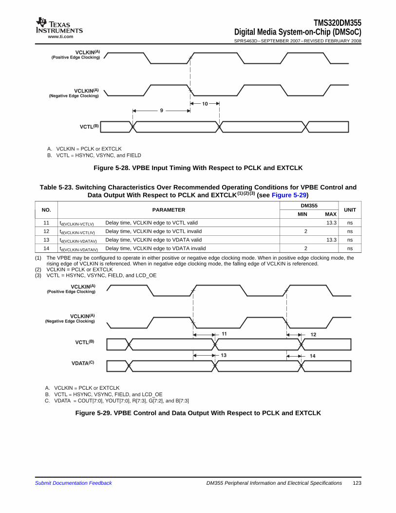
www.ti.com
VCLKIN(A)
(Positive Edge Clocking)
9
VCLKIN(A)
(Negative Edge Clocking)
10
VCTL(B)
A. VCLKIN = PCLK or EXTCLK
B. VCTL = HSYNC, VSYNC, and FIELD
VCLKIN(A)
(Positive Edge Clocking)
13
VCLKIN(A)
(Negative Edge Clocking)
11
VCTL(B)
A. VCLKIN = PCLK or EXTCLK
B. VCTL = HSYNC, VSYNC, FIELD, and LCD_OE
C. VDATA = COUT[7:0], YOUT[7:0], R[7:3], G[7:2], and B[7:3]
VDATA(C)
14
12
TMS320DM355Digital Media System-on-Chip (DMSoC)SPRS463D–SEPTEMBER 2007–REVISED FEBRUARY 2008
Figure 5-28. VPBE Input Timing With Respect to PCLK and EXTCLK
Table 5-23. Switching Characteristics Over Recommended Operating Conditions for VPBE Control andData Output With Respect to PCLK and EXTCLK (1) (2) (3) (see Figure 5-29)
DM355NO. PARAMETER UNIT
MIN MAX11 td(VCLKIN-VCTLV) Delay time, VCLKIN edge to VCTL valid 13.3 ns12 td(VCLKIN-VCTLIV) Delay time, VCLKIN edge to VCTL invalid 2 ns13 td(VCLKIN-VDATAV) Delay time, VCLKIN edge to VDATA valid 13.3 ns14 td(VCLKIN-VDATAIV) Delay time, VCLKIN edge to VDATA invalid 2 ns
(1) The VPBE may be configured to operate in either positive or negative edge clocking mode. When in positive edge clocking mode, therising edge of VCLKIN is referenced. When in negative edge clocking mode, the falling edge of VCLKIN is referenced.
(2) VCLKIN = PCLK or EXTCLK(3) VCTL = HSYNC, VSYNC, FIELD, and LCD_OE
Figure 5-29. VPBE Control and Data Output With Respect to PCLK and EXTCLK
Submit Documentation Feedback DM355 Peripheral Information and Electrical Specifications 123

www.ti.com
VCLK(Positive Edge
Clocking)
VCLK(Negative Edge
Clocking)
17
VCTL(B)
VDATA(C)
191822
21
23 24
25 26
VCLKIN(A)
A. VCLKIN = PCLK or EXTCLK
B. VCTL = HSYNC, VSYNC, FIELD, and LCD_OE
C. VDATA = COUT[7:0], YOUT[7:0], R[7:3], G[7:2], and B[7:3]
2020
5.9.2.4 DAC and Video Buffer Electrical Data/Timing
TMS320DM355Digital Media System-on-Chip (DMSoC)SPRS463D–SEPTEMBER 2007–REVISED FEBRUARY 2008
Table 5-24. Switching Characteristics Over Recommended Operating Conditions for VPBE Control andData Output With Respect to VCLK (1) (2) (see Figure 5-30)
DM355NO. PARAMETER UNIT
MIN MAX17 tc(VCLK) Cycle time, VCLK 13.33 160 ns18 tw(VCLKH) Pulse duration, VCLK high 5.7 ns19 tw(VCLKL) Pulse duration, VCLK low 5.7 ns20 tt(VCLK) Transition time, VCLK 3 ns21 td(VCLKINH-VCLKH) Delay time, VCLKIN high to VCLK high 2 12 ns22 td(VCLKINL-VCLKL) Delay time, VCLKIN low to VCLK low 2 12 ns23 td(VCLK-VCTLV) Delay time, VCLK edge to VCTL valid 4 ns24 td(VCLK-VCTLIV) Delay time, VCLK edge to VCTL invalid 0 ns25 td(VCLK-VDATAV) Delay time, VCLK edge to VDATA valid 4 ns26 td(VCLK-VDATAIV) Delay time, VCLK edge to VDATA invalid 0 ns
(1) The VPBE may be configured to operate in either positive or negative edge clocking mode. When in positive edge clocking mode, therising edge of VCLK is referenced. When in negative edge clocking mode, the falling edge of VCLK is referenced.
(2) VCLKIN = PCLK or EXTCLK. For timing specifications relating to PCLK, see Table 5-17, Timing Requirements for VPFE PCLKMaster/Slave Mode.
Figure 5-30. VPBE Control and Data Output Timing With Respect to VCLK
The DAC and video buffer can be configured in a DAC only configuration or in a DAC and video bufferconfiguration. In the DAC only configuration the internal video buffer is not used and an external videobuffer is attached to the DAC. In the DAC and video buffer configuration, the DAC and internal videobuffer are both used and a TV cable may be attached directly to the output of the video buffer. SeeFigure 5-31 and Figure 5-32 for recommenced circuits for each configuration.
DM355 Peripheral Information and Electrical Specifications124 Submit Documentation Feedback

www.ti.com
DIN <9:0>
MSB
LSB
DAC Digital Input
Example for External Circuit
Iout [mA]
1.4 mA
0
DAC Output Current
CBG0.1 Fm
VREF
Video DAC
RBIAS2550W
IBIAS
RLOAD499W
IOUT
Buffer
VFB TVOUT
TMS320DM355Digital Media System-on-Chip (DMSoC)SPRS463D–SEPTEMBER 2007–REVISED FEBRUARY 2008
A. Connect IOUT to a high-impedance video buffer device.B. Place capacitors and resistors as close as possible to the DM355.C. Configure the VDAC_CONFIG register in the system control module as follows: DINV = 0, PWD_GBZ = 1,
PWD_VBUFZ = 0, ACCUP_EN = X. See the TMS320DM35x Digital Media System-on-Chip (DMSoC) ARMSubsystem Reference Guide (literature number SPRUFB3) and the TMS320DM35x Digital Media System-on-ChipVideo Processing Back End (VPBE) Reference Guide (literature number SPRUF72) for more information onVDAC_CONFIG.
Figure 5-31. DAC Only Application Example
Submit Documentation Feedback DM355 Peripheral Information and Electrical Specifications 125

www.ti.com
DIN <9:0>
DAC Digital Input
CBG0.1 Fm
VREF
Video DAC and Buffer
RBIAS2550 Ω
IBIAS
Rfb = 1000 Ω
IOUT VFB TVOUT
Rout = 1070 Ω
TV monitor
TVOUT [V]
Video Buffer Output Voltage
MSB
LSBVOL(VIDBUF)
VOH(VIDBUF)
0
TMS320DM355Digital Media System-on-Chip (DMSoC)SPRS463D–SEPTEMBER 2007–REVISED FEBRUARY 2008
A. Place capacitors and resistors as close as possible to the DM355.B. You must use the circuit shown in this diagram. Also you must configure the VDAC_CONFIG register in the System
Control module as follows: TRESB4R4 = 0x3, TRESB4R2 = 0x8, TRESB4R1 = 0x8, TRIMBITS = 0x34, PWD_BGZ =1 (power up VREF), SPEED = 1 (faster), TVINT = don't care, PWD_VBUFZ = 1 (power up video buffer), VREFSET =don't care, ACCUP_EN = 0 (no A/C coupling), DINV = 1 (invert). See TMS320DM35x Digital Media System-on-Chip(DMSoC) ARM Subsystem Reference Guide (literature number SPRUFB3) and the TMS320DM35x Digital MediaSystem-on-Chip Video Processing Back End (VPBE) Reference Guide (literature number SPRUF72) for moreinformation on the VDAC_CONFIG register and Video Buffer.
C. For proper TVOUT voltage, you must connect the pin TVOUT directly to the TV. No A/C coupling capacitor ortermination resistor is necessary on your DM355 board. Also, it is assumed that the TV has no internal A/C couplingcapacitor but does have an internal termination resistor, as shown in this diagram. TVOUT voltage will range fromVOL(VIDBUF) to VOH(VIDBUF). See Section 4.3 for the voltage specifications.
Figure 5-32. DAC With Buffer Circuit
DM355 Peripheral Information and Electrical Specifications126 Submit Documentation Feedback

www.ti.com
5.10 USB 2.0
5.10.1 USB2.0 Electrical Data/Timing
trtf
VCRS90% VOH
10% VOL
USB_DM
USB_DP
tper − tjr
TMS320DM355Digital Media System-on-Chip (DMSoC)SPRS463D–SEPTEMBER 2007–REVISED FEBRUARY 2008
The DM355 USB2.0 peripheral supports the following features:• USB 2.0 peripheral at speeds high speed (HS: 480 Mb/s) and full speed (FS: 12 Mb/s)• USB 2.0 host at speeds HS, FS, and low speed (LS: 1.5 Mb/s)• All transfer modes (control, bulk, interrupt, and isochronous)• Four Transmit (TX) and four Receive (RX) endpoints in addition to endpoint 0• FIFO RAM
– 4K bytes shared by all endpoints.– Programmable FIFO size
• Includes a DMA sub-module that supports four TX and four RX channels of CPPI 3.0 DMAs• RNDIS mode for accelerating RNDIS type protocols using short packet termination over USB• USB OTG extensions, i.e. session request protocol (SRP) and host negotiation protocol (HNP)
The DM355 USB2.0 peripheral does not support the following features:• On-chip charge pump• High bandwidth ISO mode is not supported (triple buffering)• RNDIS mode acceleration for USB sizes that are not multiples of 64 bytes• Endpoint max USB packet sizes that do not conform to the USB 2.0 spec (for FS/LS: 8, 16, 32, 64,
and 1023 are defined; for HS: 64, 128, 512, and 1024 are defined)
Table 5-25. Switching Characteristics Over Recommended Operating Conditions for USB2.0 (seeFigure 5-33)
DM355LOW SPEED FULL SPEED HIGH SPEED (1)
NO. PARAMETER UNIT1.5 Mbps 12 Mbps 480 MbpsMIN MAX MIN MAX MIN MAX
1 tr(D) Rise time, USB_DP and USB_DM signals (2) 75 300 4 20 0.5 ns2 tf(D) Fall time, USB_DP and USB_DM signals (2) 75 300 4 20 0.5 ns3 tfrfm Rise/Fall time, matching (3) 80 125 90 111.11 %4 VCRS Output signal cross-over voltage (2) 1.3 2 1.3 2 V5 tjr(source)NT Source (Host) Driver jitter, next transition 2 2 ns
tjr(FUNC)NT Function Driver jitter, next transition 25 2 ns6 tjr(source)PT Source (Host) Driver jitter, paired transition (4) 1 1 ns
tjr(FUNC)PT Function Driver jitter, paired transition 10 1 ns7 tw(EOPT) Pulse duration, EOP transmitter 1250 1500 160 175 ns8 tw(EOPR) Pulse duration, EOP receiver 670 82 ns9 t(DRATE) Data Rate 1.5 12 480 Mb/s
10 ZDRV Driver Output Resistance – – 28 49.5 40.5 49.5 Ω
(1) For more detailed specification information, see the Universal Serial Bus Specification Revision 2.0, Chapter 7. Electrical.(2) Low Speed: CL = 200 pF, Full Speed: CL = 50 pF, High Speed: CL = 50 pF(3) tfrfm = (tr/tf) x 100. [Excluding the first transaction from the Idle state.](4) tjr = tpx(1) - tpx(0)
Figure 5-33. USB2.0 Integrated Transceiver Interface Timing
Submit Documentation Feedback DM355 Peripheral Information and Electrical Specifications 127

www.ti.com
VSS_USB_REF USB_R1
USB
10 K ±1%Ω
TMS320DM355Digital Media System-on-Chip (DMSoC)SPRS463D–SEPTEMBER 2007–REVISED FEBRUARY 2008
Figure 5-34. USB Reference Resistor Routing
DM355 Peripheral Information and Electrical Specifications128 Submit Documentation Feedback

www.ti.com
5.11 Universal Asynchronous Receiver/Transmitter (UART)
5.11.1 UART Electrical Data/Timing
TMS320DM355Digital Media System-on-Chip (DMSoC)SPRS463D–SEPTEMBER 2007–REVISED FEBRUARY 2008
The DM355 contains 3 separate UART modules (1 with hardware flow control). These modules performsserial-to-parallel conversion on data received from a peripheral device or modem, and parallel-to-serialconversion on data received from the CPU. Each UART also includes a programmable baud rategenerator capable of dividing the 24MHz reference clock by divisors from 1 to 65,535 to produce a 16 xclock driving the internal logic. The UART modules support the following features:• Frequency pre-scale values from 1 to 65,535 to generate appropriate baud rates• 16-byte storage space for both the transmitter and receiver FIFOs• Unique interrupts, one for each UART• Unique EDMA events, both received and transmitted data for each UART• 1, 4, 8, or 14 byte selectable receiver FIFO trigger level for autoflow control and DMA• Programmable auto-rts and auto-cts for autoflow control (supported on UART2)• Programmable serial data formats
– 5, 6, 7, or 8-bit characters– Even, odd, or no parity bit generation and detection– 1, 1.5, or 2 stop bit generation
• False start bit detection• Line break generation and detection• Internal diagnostic capabilities
– Loopback controls for communications link fault isolation– Break, parity, overrun, and framing error simulation
• Modem control functions: CTS, RTS (supported on UART2)
Table 5-26. Timing Requirements for UARTx Receive (see Figure 5-35)DM355
NO. UNITMIN MAX
4 tw(URXDB) Pulse duration, receive data bit (RXDn) 0.99U (1) 1.05U (1) ns5 tw(URXSB) Pulse duration, receive start bit 0.99U (1) 1.05U (1) ns
(1) U = UART baud time = 1/programmed baud rate.
Table 5-27. Switching Characteristics Over Recommended Operating Conditions for UARTx Transmit(see Figure 5-35)
DM355NO. PARAMETER UNIT
MIN MAXUART0/1 Maximum programmable baud rate 1.5
1 f(baud) MHzUART2 Maximum programmable baud rate 5
2 tw(UTXDB) Pulse duration, transmit data bit (TXDn) U - 2 (1) U + 2 (1) ns3 tw(UTXSB) Pulse duration, transmit start bit U - 2 (1) U + 2 (1) ns
(1) U = UART baud time = 1/programmed baud rate.
Submit Documentation Feedback DM355 Peripheral Information and Electrical Specifications 129

www.ti.com
3
2Start
Bit
Data Bits
UART_TXDn
UART_RXDn
5
Data Bits
Bit
Start
4
TMS320DM355Digital Media System-on-Chip (DMSoC)SPRS463D–SEPTEMBER 2007–REVISED FEBRUARY 2008
Figure 5-35. UART Transmit/Receive Timing
DM355 Peripheral Information and Electrical Specifications130 Submit Documentation Feedback

www.ti.com
5.12 Serial Port Interface (SPI)
5.12.1 SPI Electrical Data/Timing
SPIx_CLK
(Clock Polarity = 0)
1
23
SPIx_CLK
(Clock Polarity = 1)
TMS320DM355Digital Media System-on-Chip (DMSoC)SPRS463D–SEPTEMBER 2007–REVISED FEBRUARY 2008
The DM355 contains 3 separate SPI modules. These modules provide a programmable length shiftregister which allows serial communication with other SPI devices through a 3 or 4 wire interface (Clock,Data In, Data Out, and Enable). The SPI supports the following features:• Master mode operation• 2 chip selects for interfacing to multiple slave SPI devices.• 3 or 4 wire interface (Clock, Data In, Data Out, and Enable)• Unique interrupt for each SPI port• Separate DMA events for SPI Receive and Transmit• 16-bit shift register• Receive buffer register• Programmable character length (2 to 16 bits)• Programmable SPI clock frequency range• 8-bit clock prescaler• Programmable clock phase (delay or no delay)• Programmable clock polarity
The SPI modules do not support the following features:• Slave mode. Only Master mode is supported in DM355 (Master mode means that DM355 provides the
serial clock).• GPIO mode. GPIO functionality is supported by the GIO modules for those SPI pins that are
multiplexed with GPIO signals.
Table 5-28. Timing Requirements for SPI (All Modes) (1) (see Figure 5-36)DM355
NO. UNITMIN MAX
1 tc(CLK) Cycle time, SPI_CLK 37.037 ns ns2 tw(CLKH) Pulse duration, SPI_CLK high (All Master Modes) 0.45*T 0.55*T ns3 tw(CLKL) Pulse duration, SPI_CLK low (All Master Modes 0.45*T 0.55*T ns
(1) T = tc(CLK) = SPI_CLK period is equal to the SPI module clock divided by a configurable divider.
Figure 5-36. SPI_CLK Timing
Submit Documentation Feedback DM355 Peripheral Information and Electrical Specifications 131

www.ti.com
SPI_CLK(Clock Polarity = 0)
SPI_CLK(Clock Polarity = 1)
SPI_DI(Input)
SPI_DO(Output)
4
MSB IN DATA LSB IN
LSB OUTMSB OUT DATA
9
10
8
65
7
SPI_EN
11
TMS320DM355Digital Media System-on-Chip (DMSoC)SPRS463D–SEPTEMBER 2007–REVISED FEBRUARY 2008
SPI Master Mode Timings (Clock Phase = 0)
Table 5-29. Timing Requirements for SPI Master Mode [Clock Phase = 0] (1)(see Figure 5-37)DM355
NO. UNITMIN MAX
Setup time, SPI_DI (input) valid before SPI_CLK (output)4 tsu(DIV-CLKL) Clock Polarity = 0 .5P + 3 nsfalling edgeSetup time, SPI_DI (in put) valid before SPI_CLK (output)5 tsu(DIV-CLKH) Clock Polarity = 1 .5P + 3 nsrising edgeHold time, SPI_DI (input) valid after SPI_CLK (output) falling6 th(CLKL-DIV) Clock Polarity = 0 .5P + 3 nsedgeHold time, SPI_DI (input) valid after SPI_CLK (output) rising7 th(CLKH-DIV) Clock Polarity = 1 2.5P + 3 nsedge
(1) P = 1/SYSCLK2 in nanoseconds (ns). For example, if the SYSCLK2 frequency is 135 MHz, use P = 7.41 ns. See Section 3.5, DeviceClocking, for more information on the supported clock configurations of the DM355.
Table 5-30. Switching Characteristics Over Recommended Operating Conditions for SPI Master Mode[Clock Phase = 0] (see Figure 5-37)
DM355NO. PARAMETER UNIT
MIN MAXDelay time, SPI_CLK (output) rising edge to SPI_DO8 td(CLKH-DOV) Clock Polarity = 0 -4 5 ns(output) transitionDelay time, SPI_CLK (output) falling edge to SPI_DO9 td(CLKL-DOV) Clock Polarity = 1 -4 5 ns(output) transitionDelay time, SPI_EN[1:0] (output) falling edge to first SPI_CLK (output) rising or falling10 td(ENL-CLKH/L) 2P (1) (1) nsedge
P+.5C (211 td(CLKH/L-ENH) Delay time, SPI_CLK (output) rising or falling edge to SPI_EN[1:0] (output) rising edge (2) ns)
(1) The delay time can be adjusted using the SPI module register C2TDELAY. See the TMS320DM355 DMSoC Serial Peripheral Interface(SPI) User's Guide (SPRUED4).
(2) The delay time can be adjusted using the SPI module register T2CDELAY. See the TMS320DM355 DMSoC Serial Peripheral Interface(SPI) User's Guide (SPRUED4).
Figure 5-37. SPI Master Mode External Timing (Clock Phase = 0)
DM355 Peripheral Information and Electrical Specifications132 Submit Documentation Feedback

www.ti.com
SPI_CLK(Clock Polarity = 0)
SPI_CLK(Clock Polarity = 1)
SPI_DI(Input)
SPI_DO(Output)
13
MSB IN DATA LSB IN
LSB OUTMSB OUT DATA
17
15
1416
SPI_EN
19
18
TMS320DM355Digital Media System-on-Chip (DMSoC)SPRS463D–SEPTEMBER 2007–REVISED FEBRUARY 2008
SPI Master Mode Timings (Clock Phase = 1)
Table 5-31. Timing Requirements for SPI Master Mode [Clock Phase = 1] (see Figure 5-38)DM355
NO. UNITMIN MAX
Setup time, SPI_DI (input) valid before SPI_CLK (output)13 tsu(DIV-CLKL) Clock Polarity = 0 .5P + 3 nsrising edgeSetup time, SPI_DI (in put) valid before SPI_CLK (output)14 tsu(DIV-CLKH) Clock Polarity = 1 .5P + 3 nsfalling edgeHold time, SPI_DI (input) valid after SPI_CLK (output) rising15 th(CLKL-DIV) Clock Polarity = 0 .5P + 3 nsedgeHold time, SPI_DI (input) valid after SPI_CLK (output) falling16 th(CLKH-DIV) Clock Polarity = 1 .5P + 3 nsedge
Table 5-32. Switching Characteristics Over Recommended Operating Conditions for SPI Master Mode[Clock Phase = 1] (see Figure 5-38)
DM355NO. PARAMETER UNIT
MIN MAXDelay time, SPI_CLK (output) falling edge to SPI_DO17 td(CLKL-DOV) Clock Polarity = 0 -4 5 ns(output) transitionDelay time, SPI_CLK (output) rising edge to SPI_DO18 td(CLKH-DOV) Clock Polarity = 1 -4 5 ns(output) transitionDelay time, SPI_EN[1:0] (output) falling edge to first SPI_CLK (output) rising or falling 2P+.5C19 td(ENL-CLKH/L)
(1) nsedge (1)
20 td(CLKL/H-DOHz) Delay time, SPI_CLK (output) falling or rising edge to SPI_DO (output) high impedance P (2) (2) ns
(1) The delay time can be adjusted using the SPI module register C2TDELAY. See the TMS320DM355 DMSoC Serial Peripheral Interface(SPI) User's Guide (SPRUED4).
(2) The delay time can be adjusted using the SPI module register T2CDELAY. See the TMS320DM355 DMSoC Serial Peripheral Interface(SPI) User's Guide (SPRUED4).
Figure 5-38. SPI Master Mode External Timing (Clock Phase = 1)
Submit Documentation Feedback DM355 Peripheral Information and Electrical Specifications 133
www.ti.com
5.13 Inter-Integrated Circuit (I2C)
TMS320DM355Digital Media System-on-Chip (DMSoC)SPRS463D–SEPTEMBER 2007–REVISED FEBRUARY 2008
The inter-integrated circuit (I2C) module provides an interface between DM355 and other devicescompliant with Philips Semiconductors Inter-IC bus (I2C-bus) specification version 2.1 and connected byway of an I2C-bus. External components attached to this 2-wire serial bus can transmit/receive up to 8-bitdata to/from the DM355 through the I2C module.
The I2C port supports:• Compatible with Philips I2C Specification Revision 2.1 (January 2000)• Fast Mode up to 400 Kbps (no fail-safe I/O buffers)• Noise Filter to Remove Noise 50 ns or less• Seven- and Ten-Bit Device Addressing Modes• Master (Transmit/Receive) and Slave (Transmit/Receive) Functionality• Events: DMA, Interrupt, or Polling• Slew-Rate Limited Open-Drain Output Buffers
For more detailed information on the I2C peripheral, see the Documentation Support section for theDM355 Inter-Integrated Circuit (I2C) Module Reference Guide.
DM355 Peripheral Information and Electrical Specifications134 Submit Documentation Feedback

www.ti.com
5.13.1 I2C Electrical Data/Timing
5.13.1.1 Inter-Integrated Circuits (I2C) Timing
10
8
4
3
7
12
5
6 14
2
3
13
Stop Start RepeatedStart
Stop
SDA
SCL
1
11 9
TMS320DM355Digital Media System-on-Chip (DMSoC)SPRS463D–SEPTEMBER 2007–REVISED FEBRUARY 2008
Table 5-33. Timing Requirements for I2C Timings (1) (see Figure 5-39)DM355
STANDARDNO. FAST MODE UNITMODEMIN MAX MIN MAX
1 tc(SCL) Cycle time, SCL 10 2.5 µsSetup time, SCL high before SDA low (for a repeated START2 tsu(SCLH-SDAL) 4.7 0.6 µscondition)Hold time, SCL low after SDA low (for a START and a repeated3 th(SCLL-SDAL) 4 0.6 µsSTART condition)
4 tw(SCLL) Pulse duration, SCL low 4.7 1.3 µs5 tw(SCLH) Pulse duration, SCL high 4 0.6 µs6 tsu(SDAV-SCLH) Setup time, SDA valid before SCL high 250 100 (2) ns7 th(SDA-SCLL) Hold time, SDA valid after SCL low (For I2C bus™ devices) 0 (3) 0 (3) 0.9 (4) µs
Pulse duration, SDA high between STOP and START8 tw(SDAH) 4.7 1.3 µsconditions9 tr(SDA) Rise time, SDA 1000 20 + 0.1Cb
(5) 300 ns10 tr(SCL) Rise time, SCL 1000 20 + 0.1Cb
(5) 300 ns11 tf(SDA) Fall time, SDA 300 20 + 0.1Cb
(5) 300 ns12 tf(SCL) Fall time, SCL 300 20 + 0.1Cb
(5) 300 ns13 tsu(SCLH-SDAH) Setup time, SCL high before SDA high (for STOP condition) 4 0.6 µs14 tw(SP) Pulse duration, spike (must be suppressed) 0 50 ns15 Cb
(5) Capacitive load for each bus line 400 400 pF
(1) The I2C pins SDA and SCL do not feature fail-safe I/O buffers. These pins could potentially draw current when the device is powereddown.
(2) A Fast-mode I2C-bus™ device can be used in a Standard-mode I2C-bus™ system, but the requirement tsu(SDA-SCLH)≥ 250 ns must thenbe met. This will automatically be the case if the device does not stretch the LOW period of the SCL signal. If such a device does stretchthe LOW period of the SCL signal, it must output the next data bit to the SDA line tr max + tsu(SDA-SCLH)= 1000 + 250 = 1250 ns(according to the Standard-mode I2C-Bus Specification) before the SCL line is released.
(3) A device must internally provide a hold time of at least 300 ns for the SDA signal (referred to the VIHmin of the SCL signal) to bridge theundefined region of the falling edge of SCL.
(4) The maximum th(SDA-SCLL) has only to be met if the device does not stretch the low period [tw(SCLL)] of the SCL signal.(5) Cb = total capacitance of one bus line in pF. If mixed with HS-mode devices, faster fall-times are allowed.
Figure 5-39. I2C Receive Timings
Submit Documentation Feedback DM355 Peripheral Information and Electrical Specifications 135

www.ti.com
23
19
18
22
20
21
17
18
28
Stop Start RepeatedStart
Stop
SDA
SCL
16
TMS320DM355Digital Media System-on-Chip (DMSoC)SPRS463D–SEPTEMBER 2007–REVISED FEBRUARY 2008
Table 5-34. Switching Characteristics for I2C Timings (1) (see Figure 5-40)DM355
STANDARDNO. PARAMETER FAST MODE UNITMODEMIN MAX MIN MAX
16 tc(SCL) Cycle time, SCL 10 2.5 µsDelay time, SCL high to SDA low (for a repeated START17 td(SCLH-SDAL) 4.7 0.6 µscondition)Delay time, SDA low to SCL low (for a START and a repeated18 td(SDAL-SCLL) 4 0.6 µsSTART condition)
19 tw(SCLL) Pulse duration, SCL low 4.7 1.3 µs20 tw(SCLH) Pulse duration, SCL high 4 0.6 µs21 td(SDAV-SCLH) Delay time, SDA valid to SCL high 250 100 ns22 tv(SCLL-SDAV) Valid time, SDA valid after SCL low (For I2C devices) 0 0 0.9 µs
Pulse duration, SDA high between STOP and START23 tw(SDAH) 4.7 1.3 µsconditions28 td(SCLH-SDAH) Delay time, SCL high to SDA high (for STOP condition) 4 0.6 µs29 Cp Capacitance for each I2C pin 10 10 pF
(1) Cb = total capacitance of one bus line in pF. If mixed with HS-mode devices, faster fall-times are allowed.
CAUTIONThe DM355 I2C pins use a standard ±4-mA LVCMOS buffer, not the slow I/OP bufferdefined in the I2C specification. Series resistors may be necessary to reduce noise atthe system level.
Figure 5-40. I2C Transmit Timings
DM355 Peripheral Information and Electrical Specifications136 Submit Documentation Feedback
www.ti.com
5.14 Audio Serial Port (ASP)
TMS320DM355Digital Media System-on-Chip (DMSoC)SPRS463D–SEPTEMBER 2007–REVISED FEBRUARY 2008
DM355 includes two separate ASP controllers. The primary use for the audio serial port (ASP) is for audiointerface purposes. The primary audio modes that are supported by the ASP are the AC97 and IIS modes.In addition to the primary audio modes, the ASP supports general serial port receive and transmitoperation, but is not intended to be used as a high-speed interface. The ASP is backward compatible withother TI ASPs. The ASP supports the following features:• Full-duplex communication• Double-buffered data registers, which allow a continuous data stream• Independent framing and clocking for receive and transmit• External shift clock generation or an internal programmable frequency shift clock• Double-buffered data registers, which allow a continuous data stream• Independent framing and clocking for receive and transmit• Direct interface to industry-standard codecs, analog interface chips (AICs), and other serially
connected analog-to-digital (A/D) and digital-to-analog (D/A) devices• Direct interface to AC97 compliant devices (the necessary multiphase frame synchronization capability
is provided)• Direct interface to IIS compliant devices• Direct interface to SPI protocol in master mode only• A wide selection of data sizes, including 8, 12, 16, 20, 24, and 32 bits• µ-Law and A-Law companding• 8-bit data transfers with the option of LSB or MSB first• Programmable polarity for both frame synchronization and data clocks• Highly programmable internal clock and frame generation
For more detailed information on the ASP peripheral, see the Documentation Support section for theAudio Serial Port (ASP) Reference Guide.
Submit Documentation Feedback DM355 Peripheral Information and Electrical Specifications 137

www.ti.com
5.14.1 ASP Electrical Data/Timing
5.14.1.1 Audio Serial Port (ASP) Timing
TMS320DM355Digital Media System-on-Chip (DMSoC)SPRS463D–SEPTEMBER 2007–REVISED FEBRUARY 2008
Table 5-35. Timing Requirements for ASP (1) (see Figure 5-41)DM355
NO. UNITMIN MAX
15 tc(CLK) Cycle time, CLK CLK ext 38.5 or 2P (2) (3) ns16 OTG(CLKS) Pulse duration, CLKR/X high or CLKR/X low CLKS ext 19.25 or P (2) (3) (4) ns
CLKR int 215 tsu(FRH-CKRL) Setup time, external FSR high before CLKR low ns
CLKR ext 6CLKR int 0
6 th(CKRL-FRH) Hold time, external FSR high after CLKR low nsCLKR ext 6CLKR int 21
7 tsu(DRV-CKRL) Setup time, DR valid before CLKR low nsCLKR ext 6CLKR int 0
8 th(CKRL-DRV) Hold time, DR valid after CLKR low nsCLKR ext 6CLKX int 21
10 tsu(FXH-CKXL) Setup time, external FSX high before CLKX low nsCLKX ext 6CLKX int 0
11 th(CKXL-FXH) Hold time, external FSX high after CLKX low nsCLKX ext 10
(1) CLKRP = CLKXP = FSRP = FSXP = 0. If polarity of any of the signals is inverted, then the timing references of that signal are alsoinverted.
(2) P = (1/SYSCLK2), where SYSCLK2 is an output clock of PLLC1 (see Section 3.5) .(3) Use which ever value is greater.(4) The ASP does not have a duty cycle specification, just ensure that the minimum pulse duration specification is met.
DM355 Peripheral Information and Electrical Specifications138 Submit Documentation Feedback

www.ti.com
TMS320DM355Digital Media System-on-Chip (DMSoC)SPRS463D–SEPTEMBER 2007–REVISED FEBRUARY 2008
Table 5-36. Switching Characteristics Over Recommended Operating Conditions for ASP (1) (2)
(see Figure 5-41)DM355
NO. PARAMETER UNITMIN MAX
2 tc(CKRX) Cycle time, CLKR/X CLKR/X int 38.5 or 2P (3) (4) (5) ns17 td(CLKS-CLKRX) Delay time, CLKS high to internal CLKR/X CLKR/X int 1 243 tw(CKRX) Pulse duration, CLKR/X high or CLKR/X low CLKR/X int C - 1 (6) C + 1 (6) ns
CLKR int 3 254 td(CKRH-FRV) Delay time, CLKR high to internal FSR valid ns
CLKR ext 3 25CLKX int -4 8
9 td(CKXH-FXV) Delay time, CLKX high to internal FSX valid nsCLKX ext 3 25CLKX int 12 nstdis(CKXH- Disable time, DX high impedance following last data12 DXHZ) bit from CLKX high CLKX ext 12 nsCLKX int -5 12 ns
13 td(CKXH-DXV) Delay time, CLKX high to DX validCLKX ext 3 25 ns
Delay time, FSX high to DX valid FSX int 1414 td(FXH-DXV) ONLY applies when in data ns
FSX ext 25delay 0 (XDATDLY = 00b) mode
(1) CLKRP = CLKXP = FSRP = FSXP = 0. If polarity of any of the signals is inverted, then the timing references of that signal are alsoinverted.
(2) Minimum delay times also represent minimum output hold times.(3) Minimum CLKR/X cycle times must be met, even when CLKR/X is generated by an internal clock source. Minimum CLKR/X cycle times
are based on internal logic speed; the maximum usable speed may be lower due to EDMA limitations and AC timing requirements.(4) P = (1/SYSCLK2), where SYSCLK2 is an output clock of PLLC1 (see Section 3.5) .(5) Use which ever value is greater.(6) C = H or L
S = sample rate generator input clock = P if CLKSM = 1 (P = 1/SYSCLK2, where SYSCLK2 is an output of PLLC1 (see Section 3.5) )S = sample rate generator input clock = CLKS if CLKSM = 0H = CLKX high pulse width = (CLKGDV/2 + 1) * S if CLKGDV is evenH = (CLKGDV + 1)/2 * S if CLKGDV is odd or zeroL = CLKX low pulse width = (CLKGDV/2) * S if CLKGDV is evenL = (CLKGDV + 1)/2 * S if CLKGDV is odd or zeroCLKGDV should be set appropriately to ensure the ASP bit rate does not exceed the maximum limit (see footnote (3) above).
Submit Documentation Feedback DM355 Peripheral Information and Electrical Specifications 139

www.ti.com
Bit(n-1) (n-2) (n-3)
Bit 0 Bit(n-1) (n-2) (n-3)
14
1110
9
3
3
2
8
65
44
13(A)
13(A)
A. Parameter No. 13 applies to the first data bitonly when XDATDLY ≠ 0.
CLKR
FSR (int)
FSR (ext)
DR
CLKX
FSX (int)
FSX (ext)
FSX
(XDATDLY=00b)
DX
15
CLKS
1616
17
17
32
3
7
12
TMS320DM355Digital Media System-on-Chip (DMSoC)SPRS463D–SEPTEMBER 2007–REVISED FEBRUARY 2008
Figure 5-41. ASP Timing
Table 5-37. ASP as SPI Timing RequirementsCLKSTP = 10b, CLKXP = 0 (see Figure 5-42)
MASTERNO. UNIT
MIN MAXM30 tsu(DRV-CKXL) Setup time, DR valid before CLKX low 11 nsM31 th(CKXL-DRV) Hold time, DR valid after CLKX low 0 ns
Table 5-38. ASP as SPI Switching Characteristics (1) (2)
CLKSTP = 10b, CLKXP = 0 (see Figure 5-42)
MASTERNO. PARAMETER UNIT
MIN MAX38.5 orM33 tc(CKX) Cycle time, CLKX ns2P (1) (3)
M24 td(CKXL-FXH) Delay time, CLKX low to FSX high (2) T – 2 T + 3 nsM25 td(FXL-CKXH) Delay time, FSX low to CLKX high (4) L1 – 2 L1 + 2 nsM26 td(CKXH-DXV) Delay time, CLKX high to DX valid –2 6 nsM27 tdis(CKXL-DXHZ) Disable time, DX high impedance following last data bit from CLKX low L1 – 3 L1 +3 ns
(1) P = (1/SYSCLK2), where SYSCLK2 is an output clock of PLLC1 (see Section 3.5) .(2) T = CLKX period = (1 + CLKGDV) × 2P
L1 = CLKX low pulse width = T/2 when CLKGDV is odd or zero and = (CLKGDV/2) × 2P when CLKGDV is even(3) Use which ever value is greater.(4) FSX should be low before the rising edge of clock to enable slave devices and then begin a SPI transfer at the rising edge of the master
clock (CLKX).
DM355 Peripheral Information and Electrical Specifications140 Submit Documentation Feedback

www.ti.com
Bit 0 Bit(n-1) (n-2) (n-3) (n-4)
Bit 0 Bit(n-1) (n-2) (n-3) (n-4)
M31M30
M26M27
M25M24
CLKX
FSX
DX
DR
M33
TMS320DM355Digital Media System-on-Chip (DMSoC)SPRS463D–SEPTEMBER 2007–REVISED FEBRUARY 2008
Figure 5-42. ASP as SPI: CLKSTP = 10b, CLKXP = 0
Submit Documentation Feedback DM355 Peripheral Information and Electrical Specifications 141
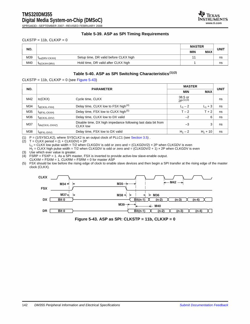
www.ti.com
Bit 0 Bit(n-1) (n-2) (n-3) (n-4)
Bit 0 Bit(n-1) (n-2) (n-3) (n-4)
M39
M36M38M37
M35M34
CLKX
FSX
DX
DR
M40
M42
TMS320DM355Digital Media System-on-Chip (DMSoC)SPRS463D–SEPTEMBER 2007–REVISED FEBRUARY 2008
Table 5-39. ASP as SPI Timing RequirementsCLKSTP = 11b, CLKXP = 0
MASTERNO. UNIT
MIN MAXM39 tsu(DRV-CKXH) Setup time, DR valid before CLKX high 11 nsM40 th(CKXH-DRV) Hold time, DR valid after CLKX high 1 ns
Table 5-40. ASP as SPI Switching Characteristics (1) (2)
CLKSTP = 11b, CLKXP = 0 (see Figure 5-43)
MASTERNO. PARAMETER UNIT
MIN MAX38.5 orM42 tc(CKX) Cycle time, CLKX ns2P (1) (3)
M34 td(CKXL-FXH) Delay time, CLKX low to FSX high (4) L1 – 2 L1 + 3 nsM35 td(FXL-CKXH) Delay time, FSX low to CLKX high (5) T – 2 T + 2 nsM36 td(CKXL-DXV) Delay time, CLKX low to DX valid –2 6 ns
Disable time, DX high impedance following last data bit fromM37 tdis(CKXL-DXHZ) –3 3 nsCLKX lowM38 td(FXL-DXV) Delay time, FSX low to DX valid H1 – 2 H1 + 10 ns
(1) P = (1/SYSCLK2), where SYSCLK2 is an output clock of PLLC1 (see Section 3.5) .(2) T = CLKX period = (1 + CLKGDV) × 2P
L1 = CLKX low pulse width = T/2 when CLKGDV is odd or zero and = (CLKGDV/2) × 2P when CLKGDV is evenH1 = CLKX high pulse width = T/2 when CLKGDV is odd or zero and = (CLKGDV/2 + 1) × 2P when CLKGDV is even
(3) Use which ever value is greater.(4) FSRP = FSXP = 1. As a SPI master, FSX is inverted to provide active-low slave-enable output.
CLKXM = FSXM = 1, CLKRM = FSRM = 0 for master ASP(5) FSX should be low before the rising edge of clock to enable slave devices and then begin a SPI transfer at the rising edge of the master
clock (CLKX).
Figure 5-43. ASP as SPI: CLKSTP = 11b, CLKXP = 0
142 DM355 Peripheral Information and Electrical Specifications Submit Documentation Feedback
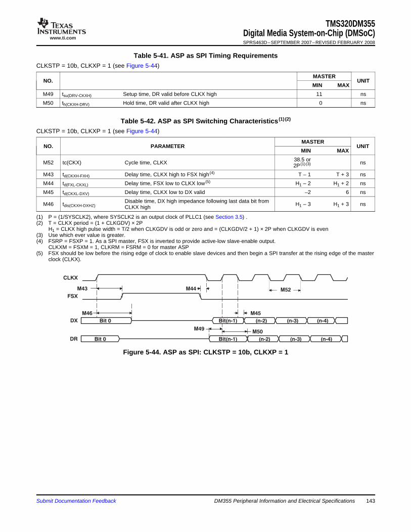
www.ti.com
Bit 0 Bit(n-1) (n-2) (n-3) (n-4)
Bit 0 Bit(n-1) (n-2) (n-3) (n-4)
M50M49
M45M46
M44M43
CLKX
FSX
DX
DR
M52
TMS320DM355Digital Media System-on-Chip (DMSoC)SPRS463D–SEPTEMBER 2007–REVISED FEBRUARY 2008
Table 5-41. ASP as SPI Timing RequirementsCLKSTP = 10b, CLKXP = 1 (see Figure 5-44)
MASTERNO. UNIT
MIN MAXM49 tsu(DRV-CKXH) Setup time, DR valid before CLKX high 11 nsM50 th(CKXH-DRV) Hold time, DR valid after CLKX high 0 ns
Table 5-42. ASP as SPI Switching Characteristics (1) (2)
CLKSTP = 10b, CLKXP = 1 (see Figure 5-44)
MASTERNO. PARAMETER UNIT
MIN MAX38.5 orM52 tc(CKX) Cycle time, CLKX ns2P (1) (3)
M43 td(CKXH-FXH) Delay time, CLKX high to FSX high (4) T – 1 T + 3 nsM44 td(FXL-CKXL) Delay time, FSX low to CLKX low (5) H1 – 2 H1 + 2 nsM45 td(CKXL-DXV) Delay time, CLKX low to DX valid –2 6 ns
Disable time, DX high impedance following last data bit fromM46 tdis(CKXH-DXHZ) H1 – 3 H1 + 3 nsCLKX high
(1) P = (1/SYSCLK2), where SYSCLK2 is an output clock of PLLC1 (see Section 3.5) .(2) T = CLKX period = (1 + CLKGDV) × 2P
H1 = CLKX high pulse width = T/2 when CLKGDV is odd or zero and = (CLKGDV/2 + 1) × 2P when CLKGDV is even(3) Use which ever value is greater.(4) FSRP = FSXP = 1. As a SPI master, FSX is inverted to provide active-low slave-enable output.
CLKXM = FSXM = 1, CLKRM = FSRM = 0 for master ASP(5) FSX should be low before the rising edge of clock to enable slave devices and then begin a SPI transfer at the rising edge of the master
clock (CLKX).
Figure 5-44. ASP as SPI: CLKSTP = 10b, CLKXP = 1
Submit Documentation Feedback DM355 Peripheral Information and Electrical Specifications 143
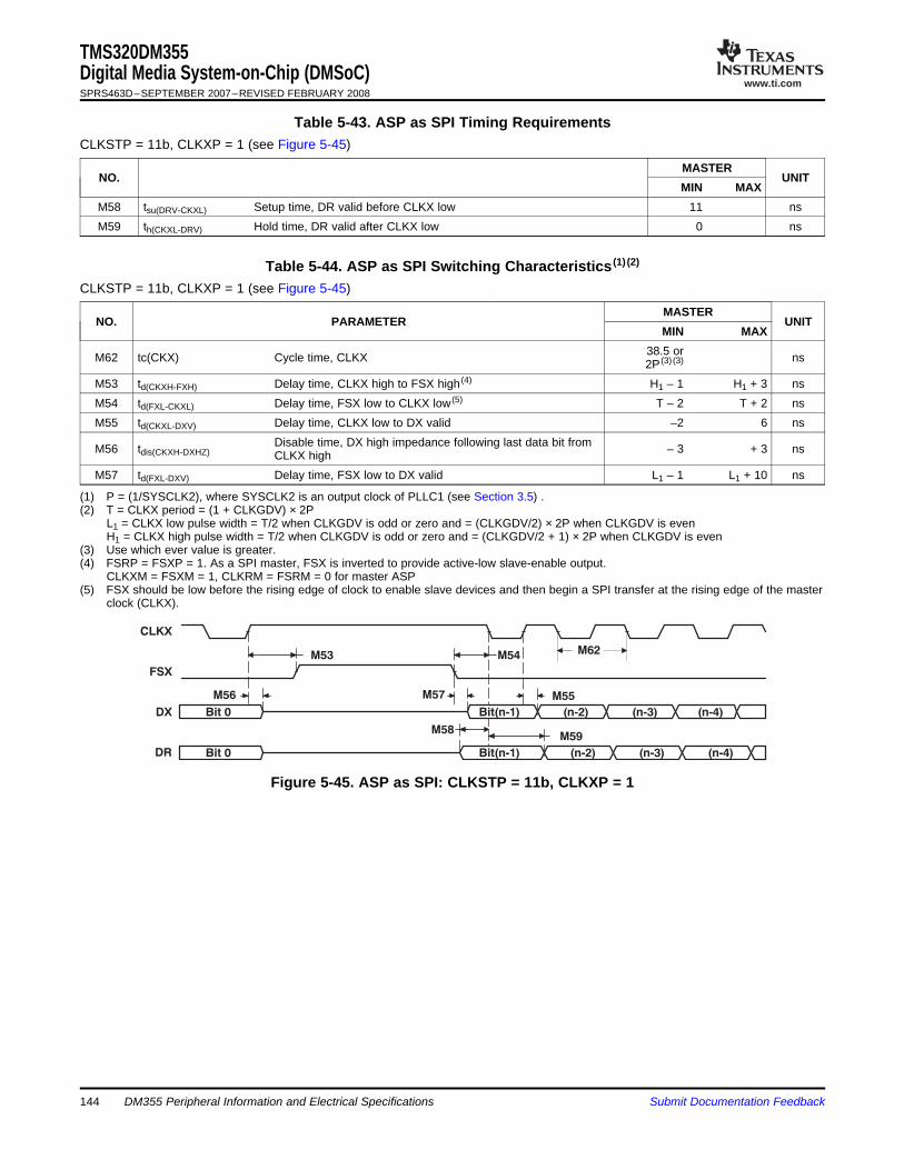
www.ti.com
Bit 0 Bit(n-1) (n-2) (n-3) (n-4)
Bit 0 Bit(n-1) (n-2) (n-3) (n-4)
M59M58
M55M57M56
M54M53
CLKX
FSX
DX
DR
M62
TMS320DM355Digital Media System-on-Chip (DMSoC)SPRS463D–SEPTEMBER 2007–REVISED FEBRUARY 2008
Table 5-43. ASP as SPI Timing RequirementsCLKSTP = 11b, CLKXP = 1 (see Figure 5-45)
MASTERNO. UNIT
MIN MAXM58 tsu(DRV-CKXL) Setup time, DR valid before CLKX low 11 nsM59 th(CKXL-DRV) Hold time, DR valid after CLKX low 0 ns
Table 5-44. ASP as SPI Switching Characteristics (1) (2)
CLKSTP = 11b, CLKXP = 1 (see Figure 5-45)
MASTERNO. PARAMETER UNIT
MIN MAX38.5 orM62 tc(CKX) Cycle time, CLKX ns2P (3) (3)
M53 td(CKXH-FXH) Delay time, CLKX high to FSX high (4) H1 – 1 H1 + 3 nsM54 td(FXL-CKXL) Delay time, FSX low to CLKX low (5) T – 2 T + 2 nsM55 td(CKXL-DXV) Delay time, CLKX low to DX valid –2 6 ns
Disable time, DX high impedance following last data bit fromM56 tdis(CKXH-DXHZ) – 3 + 3 nsCLKX highM57 td(FXL-DXV) Delay time, FSX low to DX valid L1 – 1 L1 + 10 ns
(1) P = (1/SYSCLK2), where SYSCLK2 is an output clock of PLLC1 (see Section 3.5) .(2) T = CLKX period = (1 + CLKGDV) × 2P
L1 = CLKX low pulse width = T/2 when CLKGDV is odd or zero and = (CLKGDV/2) × 2P when CLKGDV is evenH1 = CLKX high pulse width = T/2 when CLKGDV is odd or zero and = (CLKGDV/2 + 1) × 2P when CLKGDV is even
(3) Use which ever value is greater.(4) FSRP = FSXP = 1. As a SPI master, FSX is inverted to provide active-low slave-enable output.
CLKXM = FSXM = 1, CLKRM = FSRM = 0 for master ASP(5) FSX should be low before the rising edge of clock to enable slave devices and then begin a SPI transfer at the rising edge of the master
clock (CLKX).
Figure 5-45. ASP as SPI: CLKSTP = 11b, CLKXP = 1
DM355 Peripheral Information and Electrical Specifications144 Submit Documentation Feedback

www.ti.com
5.15 Timer
5.15.1 Timer Electrical Data/Timing
1
2
44
3
TIM_IN
TMS320DM355Digital Media System-on-Chip (DMSoC)SPRS463D–SEPTEMBER 2007–REVISED FEBRUARY 2008
The DM355 contains four software-programmable timers. Timer 0, Timer 1, and Timer 3 (general-purposetimers) can be programmed in 64-bit mode, dual 32-bit unchained mode, or dual 32-bit chained mode.Timer 3 supports additional features over the other timers: external clock/event input, period reload, outputevent tied to Real Time Out (RTO) module, external event capture, and timer counter register read reset.Timer 2 is used only as a watchdog timer. Timer 2 is tied to device reset.• 64-bit count-up counter• Timer modes:
– 64-bit general-purpose timer mode (Timer 0, 1, 3)– Dual 32-bit general-purpose timer mode (Timer 0, 1, 3)– Watchdog timer mode (Timer 2)
• Two possible clock sources:– Internal clock– External clock/event input via timer input pins (Timer 3)
• Three possible operation modes:– One-time operation (timer runs for one period then stops)– Continuous operation (timer automatically resets after each period)– Continuous operation with period reload (Timer 3)
• Generates interrupts to the ARM CPU• Generates sync event to EDMA• Generates output event to device reset (Timer 2)• Generates output event to Real Timer Out (RTO) module (Timer 3)• External event capture via timer input pins (Timer 3)
For more detailed information, see the TMS320DM355 DMSoC 64-bit Timer User's Guide for moreinformation (SPRUEE5).
Table 5-45. Timing Requirements for Timer Input (1) (2) (3) (see Figure 5-46)DM355
NO. UNITMIN MAX
1 tc(TIN) Cycle time, TIM_IN 4P ns2 tw(TINPH) Pulse duration, TIM_IN high 0.45C 0.55C ns3 tw(TINPL) Pulse duration, TIM_IN low 0.45C 0.55C ns4 tt(TIN) Transition time, TIM_IN 0.05C ns
(1) GPIO000, GPIO001, GPIO002, and GPIO003 can be used as external clock inputs for Timer 3. See the TMS320DM355 DMSoC 64-bitTimer User's Guide for more information (SPRUEE5).
(2) P = MXI1/CLKIN cycle time in ns. For example, when MXI1/CLKIN frequency is 24 MHz use P = 41.6 ns.(3) C = TIM_IN cycle time in ns. For example, when TIM_IN frequency is 24 MHz use C = 41.6 ns
Figure 5-46. Timer Input Timing
Submit Documentation Feedback DM355 Peripheral Information and Electrical Specifications 145

www.ti.com
5.16 Pulse Width Modulator (PWM)
5.16.1 PWM0/1/2/3 Electrical/Timing Data
PWM0/1/2/3
1
3
3
2
TMS320DM355Digital Media System-on-Chip (DMSoC)SPRS463D–SEPTEMBER 2007–REVISED FEBRUARY 2008
The DM355 contains 4 separate Pulse Width Modulator (PWM) modules. The pulse width modulator(PWM) feature is very common in embedded systems. It provides a way to generate a pulse periodicwaveform for motor control or can act as a digital-to-analog converter with some external components.This PWM peripheral is basically a timer with a period counter and a first-phase duration comparator,where bit width of the period and first-phase duration are both programmable. The Pulse Width Modulator(PWM) modules support the following features:• 32-bit period counter• 32-bit first-phase duration counter• 8-bit repeat count for one-shot operation. One-shot operation will produce N + 1 periods of the
waveform, where N is the repeat counter value.• Configurable to operate in either one-shot or continuous mode• Buffered period and first-phase duration registers• One-shot operation triggerable by hardware events with programmable edge transitions. (low-to-high or
high-to-low).• One-shot operation triggerable by the CCD VSYNC output of the video processing subsystem (VPSS),
which allows any of the PWM instantiations to be used as a CCD timer. This allows the DM355 moduleto support the functions provided by the CCD timer feature (generating strobe and shutter signals).
• One-shot operation generates N+1 periods of waveform, N being the repeat count register value• Configurable PWM output pin inactive state• Interrupt and EDMA synchronization events
Table 5-46. Switching Characteristics Over Recommended Operating Conditions for PWM0/1/2/3Outputs (1) (see Figure 5-47 and Figure 5-48)
DM355NO. PARAMETER UNIT
MIN MAX1 tw(PWMH) Pulse duration, PWMx high P ns2 tw(PWML) Pulse duration, PWMx low P ns3 tt(PWM) Transition time, PWMx .05P ns4 td(CCDC-PWMV) Delay time, CCDC(VD) trigger event to PWMx valid 10 ns
(1) P = MXI1/CLKIN cycle time in ns. For example, when MXI1/CLKIN frequency is 24 MHz use P = 41.6 ns.
Figure 5-47. PWM Output Timing
DM355 Peripheral Information and Electrical Specifications146 Submit Documentation Feedback

www.ti.com
4
VD(CCDC)
4
4
INVALID
INVALID
INVALID
VALID
VALID
VALID
PWM0
PWM1
PWM2
4
INVALID VALIDPWM3
TMS320DM355Digital Media System-on-Chip (DMSoC)SPRS463D–SEPTEMBER 2007–REVISED FEBRUARY 2008
Figure 5-48. PWM Output Delay Timing
Submit Documentation Feedback DM355 Peripheral Information and Electrical Specifications 147

www.ti.com
5.17 Real Time Out (RTO)
5.17.1 RTO Electrical/Timing Data
RTO0/1/2/3
1
3
3
2
4
TINT12/TINT34
(Timer3)
4
4
INVALID
INVALID
INVALID
VALID
VALID
VALID
RTO0
4
INVALID VALID
RTO1
RTO2
RTO3
TMS320DM355Digital Media System-on-Chip (DMSoC)SPRS463D–SEPTEMBER 2007–REVISED FEBRUARY 2008
The DM355 Real Time Out (RTO) peripheral supports the following features:• Four separate outputs• Trigger on Timer3 event
Table 5-47. Switching Characteristics Over Recommended Operating Conditions for RTO Outputs (seeFigure 5-49 and Figure 5-50)
DM355NO. PARAMETER UNIT
MIN MAX1 tw(RTOH) Pulse duration, RTOx high P ns2 tw(RTOL) Pulse duration, RTOx low P ns3 tt(RTO) Transition time, RTOx .1P ns4 td(TIMER3-RTOV) Delay time, Timer 3 (TINT12 or TINT34) trigger event to RTOx valid 10 ns
Figure 5-49. RTO Output Timing
Figure 5-50. RTO Output Delay Timing
DM355 Peripheral Information and Electrical Specifications148 Submit Documentation Feedback
www.ti.com
5.18 IEEE 1149.1 JTAG
TMS320DM355Digital Media System-on-Chip (DMSoC)SPRS463D–SEPTEMBER 2007–REVISED FEBRUARY 2008
The JTAG (1) interface is used for BSDL testing and emulation of the DM355 device.
The DM355 device requires that both TRST and RESET be asserted upon power up to be properlyinitialized. While RESET initializes the device, TRST initializes the device's emulation logic. Both resetsare required for proper operation.
While both TRST and RESET need to be asserted upon power up, only RESET needs to be released forthe device to boot properly. TRST may be asserted indefinitely for normal operation, keeping the JTAGport interface and device's emulation logic in the reset state.
TRST only needs to be released when it is necessary to use a JTAG controller to debug the device orexercise the device's boundary scan functionality. Note: TRST is synchronous and must be clocked byTCK; otherwise, the boundary scan logic may not respond as expected after TRST is asserted.
RESET must be released only in order for boundary-scan JTAG to read the variant field of IDCODEcorrectly. Other boundary-scan instructions work correctly independent of current state of RESET.
For maximum reliability, DM355 includes an internal pulldown (PD) on the TRST pin to ensure that TRSTwill always be asserted upon power up and the device's internal emulation logic will always be properlyinitialized.
JTAG controllers from Texas Instruments actively drive TRST high. However, some third-party JTAGcontrollers may not drive TRST high but expect the use of a pullup resistor on TRST.
When using this type of JTAG controller, assert TRST to intialize the device after powerup and externallydrive TRST high before attempting any emulation or boundary scan operations. Following the release ofRESET, the low-to-high transition of TRST must be "seen" to latch the state of EMU1 and EMU0. TheEMU[1:0] pins configure the device for either Boundary Scan mode or Emulation mode. For more detailedinformation, see the terminal functions section of this data sheet.
(1) IEEE Standard 1149.1-1990 Standard-Test-Access Port and Boundary Scan Architecture.
Submit Documentation Feedback DM355 Peripheral Information and Electrical Specifications 149

www.ti.com
5.18.1 JTAG Test-Port Electrical Data/Timing
RTCK
TDO
TDI
45
TMS
67
TCK
1
2 3
TMS320DM355Digital Media System-on-Chip (DMSoC)SPRS463D–SEPTEMBER 2007–REVISED FEBRUARY 2008
Table 5-48. Timing Requirements for JTAG Test Port (see Figure 5-51)DM355
NO. UNITMIN MAX
1 tc(TCK) Cycle time, TCK 20 ns2 tw(TCKH) Pulse duration, TCK high 8 ns3 tw(TCKL) Pulse duration, TCK low 8 ns4 tsu(TDIV-RTCKH) Setup time, TDI valid before RTCK high 10 ns5 th(RTCKH-TDIIV) Hold time, TDI valid after RTCK high 9 ns6 tsu(TMSV-RTCKH) Setup time, TMS valid before RTCK high 2 ns7 th(RTCKH-TMSIV) Hold time, TMS valid after RTCK high 5 ns
Figure 5-51. JTAG Input Timing
DM355 Peripheral Information and Electrical Specifications150 Submit Documentation Feedback
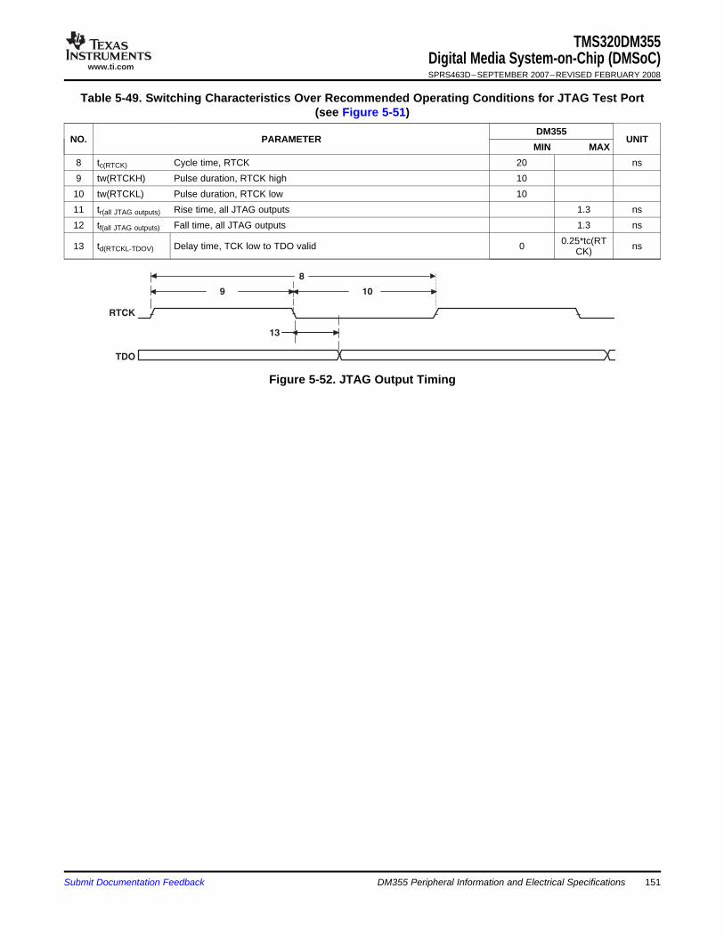
www.ti.com
RTCK
TDO
13
8
9 10
TMS320DM355Digital Media System-on-Chip (DMSoC)SPRS463D–SEPTEMBER 2007–REVISED FEBRUARY 2008
Table 5-49. Switching Characteristics Over Recommended Operating Conditions for JTAG Test Port(see Figure 5-51)
DM355NO. PARAMETER UNIT
MIN MAX8 tc(RTCK) Cycle time, RTCK 20 ns9 tw(RTCKH) Pulse duration, RTCK high 1010 tw(RTCKL) Pulse duration, RTCK low 1011 tr(all JTAG outputs) Rise time, all JTAG outputs 1.3 ns12 tf(all JTAG outputs) Fall time, all JTAG outputs 1.3 ns
0.25*tc(RT13 td(RTCKL-TDOV) Delay time, TCK low to TDO valid 0 nsCK)
Figure 5-52. JTAG Output Timing
Submit Documentation Feedback DM355 Peripheral Information and Electrical Specifications 151

www.ti.com
6 Revision History (Revision D)
TMS320DM355Digital Media System-on-Chip (DMSoC)SPRS463D–SEPTEMBER 2007–REVISED FEBRUARY 2008
This data sheet revision history highlights the technical changes made to the SPRS463C device-specificdata sheet to make it an SPRS463D revision.
Scope: Applicable updates to the DM35x DMSoC device family, specifically relating to theTMS320DM355 device, have been incorporated.• This device now supports MPEG4 only.
ADDS/CHANGES/DELETESGlobal: Updated/Changed "PRODUCT PREVIEW (PP)" to "Production Data (PD)".Global: Updated/Changed all references of "TMS320DM355 DMSoC Video Processing Back End (VPBE) User’s Guide" to "TMS320DM35xDigital Media System-on-Chip Video Processing Back End (VPBE) Reference Guide (literature number SPRUF72)".Global: Updated/Changed all references of "ARM Subsystem Reference/User guide" to "TMS320DM35x Digital Media System-on-Chip(DMSoC) ARM Subsystem Reference Guide (literature number SPRUFB3)".Global: Updated/Changed all references of "DDR/mDDR Peripheral Reference Guide" to "TMS320DM35x Digital Media System-on-Chip(DMSoC) DDR2/mDDR Memory Controller Reference Guide (literature number SPRUEH7).”Table 2-11 , GPIO Terminal Functions• Updated/Changed the description for pin L4 from “SPI: SPI2 Data In” to “SPI: SPI2 Data In-OR- SPI2 Chip select 1”.• Updated/Changed the description for pin M3 from "SPI2: Chip select” to “SPI2: Chip select 0".Table 2-17 , SPI Terminal Functions• Updated/Changed the description for pin A13 from “SPI1: Chip select” to “SPI1: Chip select 1".• Updated/Changed the description for pin M3 from “SPI1: Chip select” to “SPI1: Chip select 0”• Updated/Changed the description for pin L4 from “SPI: SPI2 Data In” to “SPI: SPI2 Data In-OR- SPI2 Chip select 1”Table 2-23 , DM355 Pin Descriptions• Updated/Changed the description for pin M3 from “SPI1: Chip select” to “SPI1: Chip select 0”• Updated/Changed the description for pin L4 from “SPI: SPI2 Data In” to “SPI: SPI2 Data In-OR- SPI2 Chip select 1”• Updated/Changed the DESCRIPTION text for DDR_DQM[1] (U15) from "Data mask outputs: DQM0: For DDR_DQ[7:0]" to "Data
mask outputs: DDR_DQM1: For DDR_DQ[15:8]".• Updated/Changed the DESCRIPTION text for DDR_DQM[0] (T12) from "Data mask outputs: DQM1: For DDR_DQ[15:8]" to "Data
mask outputs: DDR_DQM0: For DDR_DQ[7:0]".• Updated/Changed the DESCRIPTION text for pin DDR_DQS[1] (V15) from "DQS1: For DDR_DQ[15:8]" to " DDR_DQS1: For
DDR_DQ[15:8]".• Updated/Changed the DESCRIPTION text for pin DDR_DQS[0] (V12) from "DQS0: For DDR_DQ[7:0]" to "DDR_DQS0: For
DDR_DQ[7:0]".Table 3-19• Updated/Changed “MMC0RXEVT or MEMSTK:MSEVT” to "MMCORXEVT" for EDMA Channel 26Section 5.9.1.1 , CCD Controller (CCDC)• Updated/Changed the bullet "Support for ITU-R BT.656 standard format...".• Updated/Changed the bullet "Support for generating output to range from...".Section 5.10, USB 2.0• Updated/Changed "The DM355 USB2.0 ..." paragraph.• Updated/Changed "4K byte ..." bullet.Section 5.14 , Audio Serial Port (ASP)• Added the bullet "Direct interface to SPI protocol...".Section 5.16 , Pulse Width Modulator (PWM)• Deleted DM320 from the bullet "One-shot operation triggerable by the CCD VSYNC output of the video...".Section 7.1, Thermal Resistance Characteristics (PBGA Package) [ZCE]• Updated/Changed the thermal resistance characteristics.
Revision History (Revision D)152 Submit Documentation Feedback

www.ti.com
7 Mechanical Data
7.1 Thermal Data for ZCE
7.1.1 Packaging Information
TMS320DM355Digital Media System-on-Chip (DMSoC)SPRS463D–SEPTEMBER 2007–REVISED FEBRUARY 2008
The following table(s) show the thermal resistance characteristics for the PBGA – ZCE mechanicalpackage. Note that micro-vias are not required. Contact your TI representative for routingrecommendations.
The following table shows the thermal resistance characteristics for the PBGA – ZCE mechanicalpackage.
Table 7-1. Thermal Resistance Characteristics (PBGA Package) [ZCE]NO. °C/W (1)
1 RΘJC Junction-to-case 7.22 RΘJB Junction-to-board 11.43 RΘJA Junction-to-free air 27.04 PsiJT Junction-to-package top 0.15 PsiJB Junction-to-board 11.3
(1) The junction-to-case measurement was conducted in a JEDEC defined 2S2P system and will change based on environment as well asapplication. For more information, see these three EIA/JEDEC standards:• EIA/JESD51-2, Integrated Circuits Thermal Test Method Environment Conditions - Natural Convection (Still Air)• EIA/JESD51-3, Low Effective Thermal Conductivity Test Board for Leaded Surface Mount Packages• JESD51-7, High Effective Thermal Conductivity Test Board for Leaded Surface Mount Packages
The following packaging information and addendum reflect the most current data available for thedesignated device(s). This data is subject to change without notice and without revision of this document.Note that micro-vias are not required for this package.
Submit Documentation Feedback Mechanical Data 153

PACKAGING INFORMATION
Orderable Device Status (1) PackageType
PackageDrawing
Pins PackageQty
Eco Plan (2) Lead/Ball Finish MSL Peak Temp (3)
TMS320DM355ZCE216 ACTIVE BGA ZCE 337 200 Pb-Free(RoHS)
SNAGCU Level-3-260C-168 HR
TMS320DM355ZCE270 ACTIVE BGA ZCE 337 200 Pb-Free(RoHS)
SNAGCU Level-3-260C-168 HR
TMX320DM355ZCE216 ACTIVE BGA ZCE 337 TBD Call TI Call TI
TMX320DM355ZCE270 ACTIVE BGA ZCE 337 TBD Call TI Call TI
(1) The marketing status values are defined as follows:ACTIVE: Product device recommended for new designs.LIFEBUY: TI has announced that the device will be discontinued, and a lifetime-buy period is in effect.NRND: Not recommended for new designs. Device is in production to support existing customers, but TI does not recommend using this part ina new design.PREVIEW: Device has been announced but is not in production. Samples may or may not be available.OBSOLETE: TI has discontinued the production of the device.
(2) Eco Plan - The planned eco-friendly classification: Pb-Free (RoHS), Pb-Free (RoHS Exempt), or Green (RoHS & no Sb/Br) - please checkhttp://www.ti.com/productcontent for the latest availability information and additional product content details.TBD: The Pb-Free/Green conversion plan has not been defined.Pb-Free (RoHS): TI's terms "Lead-Free" or "Pb-Free" mean semiconductor products that are compatible with the current RoHS requirementsfor all 6 substances, including the requirement that lead not exceed 0.1% by weight in homogeneous materials. Where designed to be solderedat high temperatures, TI Pb-Free products are suitable for use in specified lead-free processes.Pb-Free (RoHS Exempt): This component has a RoHS exemption for either 1) lead-based flip-chip solder bumps used between the die andpackage, or 2) lead-based die adhesive used between the die and leadframe. The component is otherwise considered Pb-Free (RoHScompatible) as defined above.Green (RoHS & no Sb/Br): TI defines "Green" to mean Pb-Free (RoHS compatible), and free of Bromine (Br) and Antimony (Sb) based flameretardants (Br or Sb do not exceed 0.1% by weight in homogeneous material)
(3) MSL, Peak Temp. -- The Moisture Sensitivity Level rating according to the JEDEC industry standard classifications, and peak soldertemperature.
Important Information and Disclaimer:The information provided on this page represents TI's knowledge and belief as of the date that it isprovided. TI bases its knowledge and belief on information provided by third parties, and makes no representation or warranty as to theaccuracy of such information. Efforts are underway to better integrate information from third parties. TI has taken and continues to takereasonable steps to provide representative and accurate information but may not have conducted destructive testing or chemical analysis onincoming materials and chemicals. TI and TI suppliers consider certain information to be proprietary, and thus CAS numbers and other limitedinformation may not be available for release.
In no event shall TI's liability arising out of such information exceed the total purchase price of the TI part(s) at issue in this document sold by TIto Customer on an annual basis.
PACKAGE OPTION ADDENDUM
www.ti.com 28-Mar-2008
Addendum-Page 1
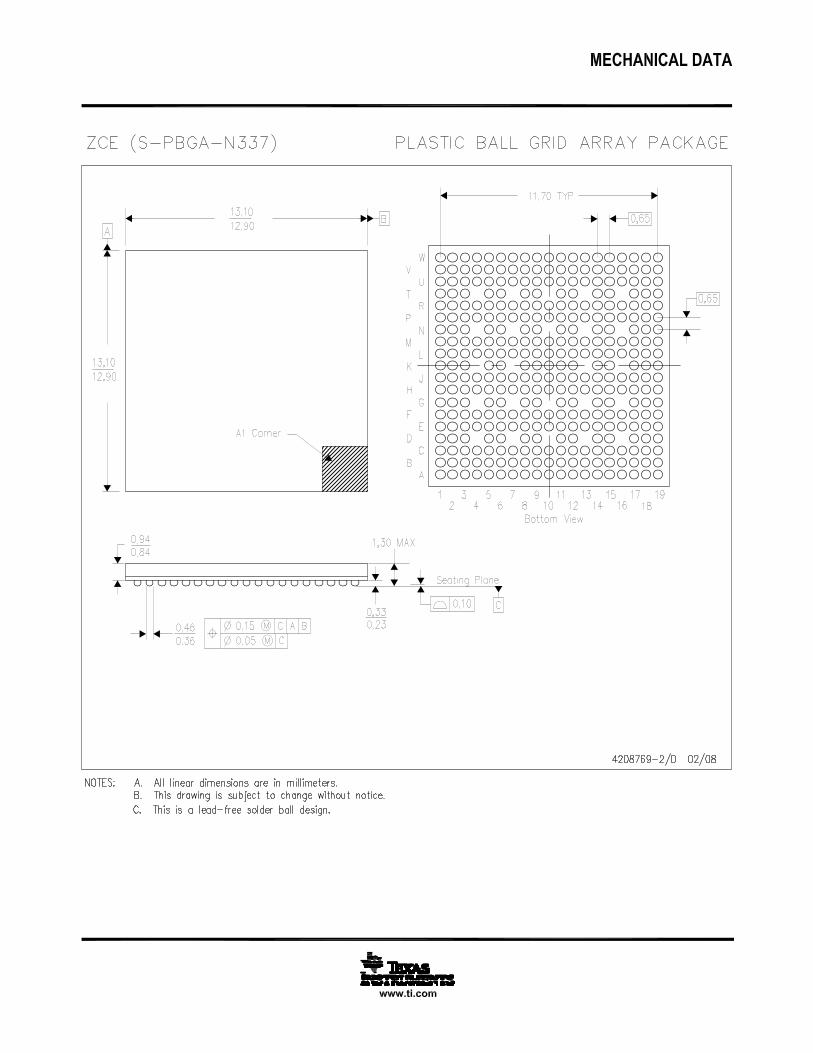

IMPORTANT NOTICETexas Instruments Incorporated and its subsidiaries (TI) reserve the right to make corrections, modifications, enhancements, improvements,and other changes to its products and services at any time and to discontinue any product or service without notice. Customers shouldobtain the latest relevant information before placing orders and should verify that such information is current and complete. All products aresold subject to TI’s terms and conditions of sale supplied at the time of order acknowledgment.TI warrants performance of its hardware products to the specifications applicable at the time of sale in accordance with TI’s standardwarranty. Testing and other quality control techniques are used to the extent TI deems necessary to support this warranty. Except wheremandated by government requirements, testing of all parameters of each product is not necessarily performed.TI assumes no liability for applications assistance or customer product design. Customers are responsible for their products andapplications using TI components. To minimize the risks associated with customer products and applications, customers should provideadequate design and operating safeguards.TI does not warrant or represent that any license, either express or implied, is granted under any TI patent right, copyright, mask work right,or other TI intellectual property right relating to any combination, machine, or process in which TI products or services are used. Informationpublished by TI regarding third-party products or services does not constitute a license from TI to use such products or services or awarranty or endorsement thereof. Use of such information may require a license from a third party under the patents or other intellectualproperty of the third party, or a license from TI under the patents or other intellectual property of TI.Reproduction of TI information in TI data books or data sheets is permissible only if reproduction is without alteration and is accompaniedby all associated warranties, conditions, limitations, and notices. Reproduction of this information with alteration is an unfair and deceptivebusiness practice. TI is not responsible or liable for such altered documentation. Information of third parties may be subject to additionalrestrictions.Resale of TI products or services with statements different from or beyond the parameters stated by TI for that product or service voids allexpress and any implied warranties for the associated TI product or service and is an unfair and deceptive business practice. TI is notresponsible or liable for any such statements.TI products are not authorized for use in safety-critical applications (such as life support) where a failure of the TI product would reasonablybe expected to cause severe personal injury or death, unless officers of the parties have executed an agreement specifically governingsuch use. Buyers represent that they have all necessary expertise in the safety and regulatory ramifications of their applications, andacknowledge and agree that they are solely responsible for all legal, regulatory and safety-related requirements concerning their productsand any use of TI products in such safety-critical applications, notwithstanding any applications-related information or support that may beprovided by TI. Further, Buyers must fully indemnify TI and its representatives against any damages arising out of the use of TI products insuch safety-critical applications.TI products are neither designed nor intended for use in military/aerospace applications or environments unless the TI products arespecifically designated by TI as military-grade or "enhanced plastic." Only products designated by TI as military-grade meet militaryspecifications. Buyers acknowledge and agree that any such use of TI products which TI has not designated as military-grade is solely atthe Buyer's risk, and that they are solely responsible for compliance with all legal and regulatory requirements in connection with such use.TI products are neither designed nor intended for use in automotive applications or environments unless the specific TI products aredesignated by TI as compliant with ISO/TS 16949 requirements. Buyers acknowledge and agree that, if they use any non-designatedproducts in automotive applications, TI will not be responsible for any failure to meet such requirements.Following are URLs where you can obtain information on other Texas Instruments products and application solutions:Products ApplicationsAmplifiers amplifier.ti.com Audio www.ti.com/audioData Converters dataconverter.ti.com Automotive www.ti.com/automotiveDSP dsp.ti.com Broadband www.ti.com/broadbandClocks and Timers www.ti.com/clocks Digital Control www.ti.com/digitalcontrolInterface interface.ti.com Medical www.ti.com/medicalLogic logic.ti.com Military www.ti.com/militaryPower Mgmt power.ti.com Optical Networking www.ti.com/opticalnetworkMicrocontrollers microcontroller.ti.com Security www.ti.com/securityRFID www.ti-rfid.com Telephony www.ti.com/telephonyRF/IF and ZigBee® Solutions www.ti.com/lprf Video & Imaging www.ti.com/video
Wireless www.ti.com/wireless
Mailing Address: Texas Instruments, Post Office Box 655303, Dallas, Texas 75265Copyright © 2008, Texas Instruments Incorporated