Embed Size (px)
Citation preview
TMS320F/C24x DSP ControllersReference Guide
CPU and Instruction Set
Literature Number: SPRU160CJune 1999
Printed on Recycled Paper
IMPORTANT NOTICE
Texas Instruments and its subsidiaries (TI) reserve the right to make changes to their productsor to discontinue any product or service without notice, and advise customers to obtain the latestversion of relevant information to verify, before placing orders, that information being relied onis current and complete. All products are sold subject to the terms and conditions of sale suppliedat the time of order acknowledgement, including those pertaining to warranty, patentinfringement, and limitation of liability.
TI warrants performance of its semiconductor products to the specifications applicable at thetime of sale in accordance with TI’s standard warranty. Testing and other quality controltechniques are utilized to the extent TI deems necessary to support this warranty. Specific testingof all parameters of each device is not necessarily performed, except those mandated bygovernment requirements.
CERTAIN APPLICATIONS USING SEMICONDUCTOR PRODUCTS MAY INVOLVEPOTENTIAL RISKS OF DEATH, PERSONAL INJURY, OR SEVERE PROPERTY ORENVIRONMENTAL DAMAGE (“CRITICAL APPLICATIONS”). TI SEMICONDUCTORPRODUCTS ARE NOT DESIGNED, AUTHORIZED, OR WARRANTED TO BE SUITABLE FORUSE IN LIFE-SUPPORT DEVICES OR SYSTEMS OR OTHER CRITICAL APPLICATIONS.INCLUSION OF TI PRODUCTS IN SUCH APPLICATIONS IS UNDERSTOOD TO BE FULLYAT THE CUSTOMER’S RISK.
In order to minimize risks associated with the customer’s applications, adequate design andoperating safeguards must be provided by the customer to minimize inherent or proceduralhazards.
TI assumes no liability for applications assistance or customer product design. TI does notwarrant or represent that any license, either express or implied, is granted under any patent right,copyright, mask work right, or other intellectual property right of TI covering or relating to anycombination, machine, or process in which such semiconductor products or services might beor are used. TI’s publication of information regarding any third party’s products or services doesnot constitute TI’s approval, warranty or endorsement thereof.
Copyright 1999, Texas Instruments Incorporated
iii
Preface
Read This First
About This Manual
The purpose of this user’s guide is to assist you, the hardware or software en-gineer, in developing applications using the TMS320F/C240,F/C24x digitalsignal processors (DSPs). This book provides CPU, hardware, and instructionset details for these devices, and explains the DSP core that is common to allTMS320F/C24x DSP controllers; and consequently, is common to the devicesdescribed in this manual.
Throughout this book, the TMS320F/C240,F/C24x devices are generally re-ferred to as ’24x.
For information about ’24x peripherals, see TMS320F/C240 DSP Controllers,Peripheral Library and Specific Devices (literature number SPRU161), orTMS320F243/F241/C242 DSP Controllers System and Peripherals Refer-ence Guide (literature number SPRU276).
Notational Conventions
This document uses the following conventions:
Program listings and program examples are shown in a special type-face .
Here is a segment of a program listing:
OUTPUT LDP #6 ;select data page 6BLDD #300, 20h ;move data at address 300h to 320hRET
Hexadecimal numbers are represented with a lowercase letter h followingthe number. For example, 7400h or 743Fh.
In syntax descriptions, the instruction is in a bold typeface andparameters are in an italic typeface. Portions of a syntax in bold must beentered as shown; portions of a syntax in italics describe the type ofinformation that you specify. Here is an example of an instruction syntax:
BLDD source, destination
BLDD is the instruction and has two parameters, source and destination.When you use BLDD , the first parameter must be an actual data memory
Information About Cautions
iv
source address and the second parameter must be a destination address.A comma and a space (optional) must separate the two addresses.
Square brackets, [ ], identify an optional parameter. If you use an optionalparameter, specify the information within the brackets; do not type thebrackets themselves. When you specify more than one optional parame-ter from a list, you separate them with a comma and a space. Here is asample syntax:
BLDD source, destination [, ARn]
BLDD is the instruction. The two required operands are source anddestination, and the optional operand is ARn. AR is bold and n is italic; ifyou choose to use ARn, you must type the letters A and R and then supplya chosen value for n (in this case, a value from 0 to 7). Here is an example:
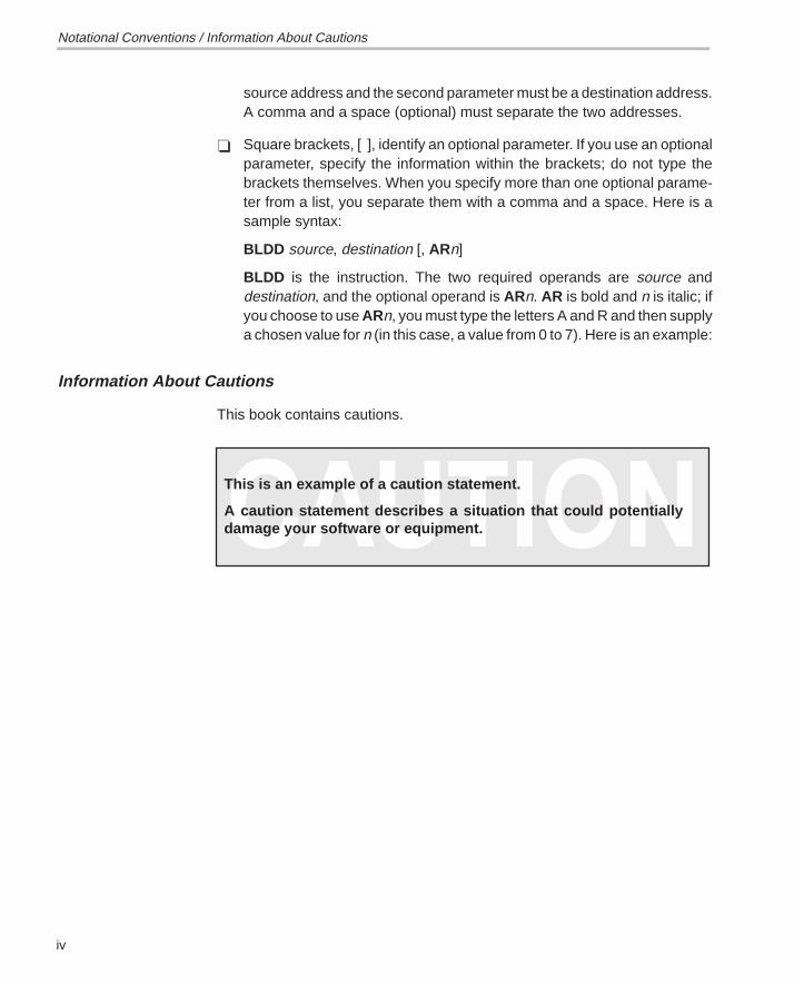
Information About Cautions
This book contains cautions.
This is an example of a caution statement.
A caution statement describes a situation that could potentiallydamage your software or equipment.
Notational Conventions / Information About Cautions
Related Documentation from Texas Instruments
vRead This First
Related Documentation from Texas Instruments
The following books describe the ’C24x and related support tools. To obtaina copy of any of these TI documents, call the Texas Instruments LiteratureResponse Center at (800) 477–8924. When ordering, please identify the bookby its title and literature number. Many of these documents are located on theinternet at http://www.ti.com.
TMS320F/C240 DSP Controllers Peripheral Library and Specific DevicesReference Guide (literature number SPRU161) describes theperipherals available on the TMS320F/C240 digital signal processorcontrollers and their operation. Also described are specific deviceconfigurations of the ’C24x family.
TMS320F243/F241/C242 DSP Controllers System and PeripheralsReference Guide (literature number SPRU276) describes thearchitecture, system hardware, peripherals, and general operation of theTMS320F243, ’F241, and ’C242 digital signal processor (DSP)controllers.
TMS320C240, TMS320F240 DSP Controllers (literature number SPRS042)data sheet contains the electrical and timing specifications for thesedevices, as well as signal descriptions and pinouts for all of the availablepackages.
TMS320F20x/F24x Embedded Flash Memory Technical Reference(literature number SPRU282) Describes the operation of the embeddedflash EEPROM module on the TMS320F20x/F24x digital signalprocessor (DSP) devices and provides sample code that you can use todevelop your own software.
TMS320C1x/C2x/C2xx/C5x Code Generation Tools Getting StartedGuide (literature number SPRU121) describes how to install theTMS320C1x, TMS320C2x, TMS320C2xx, and TMS320C5x assemblylanguage tools and the C compiler for the ’C1x, ’C2x, ’C2xx, and ’C5x de-vices. The installations for MS-DOS , OS/2 , SunOS , and Solarissystems are covered.
TMS320C1x/C2x/C2xx/C5x Assembly Language Tools User’s Guide (lit-erature number SPRU018) describes the assembly language tools (as-sembler, linker, and other tools used to develop assembly languagecode), assembler directives, macros, common object file format, andsymbolic debugging directives for the ’C1x, ’C2x, ’C2xx, and ’C5x gen-erations of devices.
Related Documentation from Texas Instruments
vi
TMS320C2x/C2xx/C5x Optimizing C Compiler User’s Guide (literaturenumber SPRU024) describes the ’C2x/C2xx/C5x C compiler. This Ccompiler accepts ANSI standard C source code and produces TMS320assembly language source code for the ’C2x, ’C2xx, and ’C5x genera-tions of devices.
TMS320C2xx C Source Debugger User’s Guide (literature numberSPRU151) tells you how to invoke the ’C2xx emulator and simulator ver-sions of the C source debugger interface. This book discusses variousaspects of the debugger interface, including window management, com-mand entry, code execution, data management, and breakpoints. It alsoincludes a tutorial that introduces basic debugger functionality.
TMS320C2xx Simulator Getting Started (literature number SPRU137)describes how to install the TMS320C2xx simulator and the C sourcedebugger for the ’C2xx. The installation for MS-DOS , PC-DOS ,SunOS , Solaris , and HP-UX systems is covered.
TMS320C2xx Emulator Getting Started Guide (literature numberSPRU209) tells you how to install the Windows 3.1 and Windows 95versions of the ’C2xx emulator and C source debugger interface.
XDS51x Emulator Installation Guide (literature number SPNU070)describes the installation of the XDS510 , XDS510PP , andXDS510WS emulator controllers. The installation of the XDS511emulator is also described.
XDS522/XDS522A Emulation System Installation Guide (literature num-ber SPRU171) describes the installation of the emulation system.Instructions include how to install the hardware and software for theXDS522 and XDS522A .
XDS522A Emulation System User’s Guide (literature number SPRU169)tells you how to use the XDS522A emulation system. This book de-scribes the operation of the breakpoint, tracing, and timing functionalityin the XDS522A emulation system. This book also discusses BTTsoftware interface and includes a tutorial that uses step-by-stepinstructions to demonstrate how to use the XDS522A emulation system.
XDS522A Emulation System Online Help (literature number SPRC002) isan online help file that provides descriptions of the BTT software user in-terface, menus, and dialog boxes.
JTAG/MPSD Emulation Technical Reference (literature number SPDU079)provides the design requirements of the XDS510 emulator controller,discusses JTAG designs (based on the IEEE 1149.1 standard), andmodular port scan device (MPSD) designs.
Related Technical Articles
viiRead This First
TMS320 DSP Development Support Reference Guide (literature numberSPRU011) describes the TMS320 family of digital signal processors andthe tools that support these devices. Included are code-generation tools(compilers, assemblers, linkers, etc.) and system integration and debugtools (simulators, emulators, evaluation modules, etc.). Also covered areavailable documentation, seminars, the university program, and factoryrepair and exchange.
TMS320 DSP Designer’s Notebook: Volume 1 (literature numberSPRT125) presents solutions to common design problems using ’C2x,’C3x, ’C4x, ’C5x, and other TI DSPs.
TMS320 Third-Party Support Reference Guide (literature numberSPRU052) alphabetically lists over 100 third parties that provide variousproducts that serve the family of TMS320 digital signal processors. Amyriad of products and applications are offered—software and hardwaredevelopment tools, speech recognition, image processing, noise can-cellation, modems, etc.
Related Technical Articles
The following technical articles contain useful information regarding designs,operations, and applications for signal-processing systems. These articlessupplement the material in this book.
“A Greener World Through DSP Controllers”, Panos Papamichalis, DSP &Multimedia Technology, September 1994.
“A Single-Chip Multiprocessor DSP for Image Processing—TMS320C80”,Dr. Ing. Dung Tu, Industrie Elektronik, Germany, March 1995.
“Application Guide with DSP Leading-Edge Technology”, Y. Nishikori,M. Hattori, T. Fukuhara, R.Tanaka, M. Shimoda, I. Kudo, A.Yanagitani,H. Miyaguchi, et al., Electronics Engineering, November 1995.
“Approaching the No-Power Barrier”, Jon Bradley and Gene Frantz, ElectronicDesign, January 9, 1995.
“Beware of BAT: DSPs Add Brilliance to New Weapons Systems”, PanosPapamichalis, DSP & Multimedia Technology, October 1994.
“Choose DSPs for PC Signal Processing”, Panos Papamichalis, DSP &Multimedia Technology, January/February 1995.
“Developing Nations Take Shine to Wireless”, Russell MacDonald, KaraSchmidt and Kim Higden, EE Times, October 2, 1995.
Related Documentation from Texas Instruments / Related Technical Articles
Related Technical Articles
viii
“Digital Signal Processing Solutions Target Vertical Application Markets”, RonWages, ECN, September 1995.
“Digital Signal Processors Boost Drive Performance”, Tim Adcock, DataStorage, September/October 1995.
“DSP and Speech Recognition, An Origin of the Species”, PanosPapamichalis, DSP & Multimedia Technology, July 1994.
“DSP Design Takes Top-Down Approach”, Andy Fritsch and Kim Asal, DSPSeries Part III, EE Times, July 17, 1995.
“DSPs Advance Low-Cost ‘Green’ Control”, Gregg Bennett, DSP Series PartII, EE Times, April 17, 1995.
“DSPs Do Best on Multimedia Applications”, Doug Rasor, Asian ComputerWorld, October 9–16, 1995.
“DSPs: Speech Recognition Technology Enablers”, Gene Frantz and GreggBennett, I&CS, May 1995.
“Easing JTAG Testing of Parallel-Processor Projects”, Tony Coomes, AndyFritsch, and Reid Tatge, Asian Electronics Engineer, Manila, Philippines,November 1995.
“Fixed or Floating? A Pointed Question in DSPs”, Jim Larimer and DanielChen, EDN, August 3, 1995.
“Function-Focused Chipsets: Up the DSP Integration Core”, PanosPapamichalis, DSP & Multimedia Technology, March/April 1995.
“GSM: Standard, Strategien und Systemchips”, Edgar Auslander, ElektronikPraxis, Germany, October 6, 1995.
“High Tech Copiers to Improve Images and Reduce Paperwork”, Karl Guttag,Document Management, July/August 1995.
“Host-Enabled Multimedia: Brought to You by DSP Solutions”, PanosPapamichalis, DSP & Multimedia Technology, September/October 1995.
“Integration Shrinks Digital Cellular Telephone Designs”, Fred Cohen andMike McMahan, Wireless System Design, November 1994.
“On-Chip Multiprocessing Melds DSPs”, Karl Guttag and Doug Deao, DSPSeries Part III, EE Times, July 18, 1994.
“Real-Time Control”, Gregg Bennett, Appliance Manufacturer, May 1995.
“Speech Recognition”, P.K. Rajasekaran and Mike McMahan, WirelessDesign & Development, May 1995.
Trademarks
ixRead This First
“Telecom Future Driven by Reduced Milliwatts per DSP Function”, PanosPapamichalis, DSP & Multimedia Technology, May/June 1995.
“The Digital Signal Processor Development Environment”, Greg Peake,Embedded System Engineering, United Kingdom, February 1995.
“The Growing Spectrum of Custom DSPs”, Gene Frantz and Kun Lin, DSPSeries Part II, EE Times, April 18, 1994.
“The Wide World of DSPs, ” Jim Larimer, Design News, June 27, 1994.
“Third-Party Support Drives DSP Development for Uninitiated and ExpertsAlike”, Panos Papamichalis, DSP & Multimedia Technology, December1994/January 1995.
“Toward an Era of Economical DSPs”, John Cooper, DSP Series Part I, EETimes, Jan. 23, 1995.
Trademarks
HP-UX is a trademark of Hewlett-Packard Company.
MS-DOS and Windows are registered trademarks of Microsoft Corporation.
OS/2, PC, and PC-DOS are trademarks of International Business MachinesCorporation.
PAL is a registered trademark of Advanced Micro Devices, Inc.
Solaris and SunOS are trademarks of Sun Microsystems, Inc.
320 Hotline On-line, TI, XDS510, XDS510PP, XDS510WS, XDS511, XDS522,and XDS522A are trademarks of Texas Instruments Incorporated.
Related Technical Articles / Trademarks
Contents
xi
Contents
1 Introduction 1-1. . . . . . . . . . . . . . . . . . . . . . . . . . . . . . . . . . . . . . . . . . . . . . . . . . . . . . . . . . . . . . . . . . . . . Summarizes the TMS320 family of products. Introduces the TMS320C24x DSP controller andlists its key features.
1.1 TMS320 Family Overview 1-2. . . . . . . . . . . . . . . . . . . . . . . . . . . . . . . . . . . . . . . . . . . . . . . . . . . 1.2 TMS320C24x Series of DSP Controllers 1-5. . . . . . . . . . . . . . . . . . . . . . . . . . . . . . . . . . . . . . .
2 Architectural Overview 2-1. . . . . . . . . . . . . . . . . . . . . . . . . . . . . . . . . . . . . . . . . . . . . . . . . . . . . . . . . . . Summarizes the TMS320C24x architecture and provides an overview of the CPU, address andbus structure, program-control logic, on-chip peripherals, and scanning logic.
2.1 Architecture Summary 2-2. . . . . . . . . . . . . . . . . . . . . . . . . . . . . . . . . . . . . . . . . . . . . . . . . . . . . . . 2.2 ’C24x CPU Internal Bus Structure 2-4. . . . . . . . . . . . . . . . . . . . . . . . . . . . . . . . . . . . . . . . . . . . . 2.3 Memory 2-5. . . . . . . . . . . . . . . . . . . . . . . . . . . . . . . . . . . . . . . . . . . . . . . . . . . . . . . . . . . . . . . . . . .
2.3.1 On-Chip Dual-Access RAM (DARAM) 2-5. . . . . . . . . . . . . . . . . . . . . . . . . . . . . . . . . . 2.3.2 Flash EEPROM 2-6. . . . . . . . . . . . . . . . . . . . . . . . . . . . . . . . . . . . . . . . . . . . . . . . . . . . . 2.3.3 Flash Serial Loader 2-6. . . . . . . . . . . . . . . . . . . . . . . . . . . . . . . . . . . . . . . . . . . . . . . . . . 2.3.4 Factory-Masked ROM 2-6. . . . . . . . . . . . . . . . . . . . . . . . . . . . . . . . . . . . . . . . . . . . . . . . 2.3.5 External Memory Interface Module 2-7. . . . . . . . . . . . . . . . . . . . . . . . . . . . . . . . . . . . .
2.4 Central Processing Unit 2-8. . . . . . . . . . . . . . . . . . . . . . . . . . . . . . . . . . . . . . . . . . . . . . . . . . . . . 2.4.1 Central Arithmetic Logic Unit (CALU) and Accumulator 2-8. . . . . . . . . . . . . . . . . . . 2.4.2 Scaling Shifters 2-8. . . . . . . . . . . . . . . . . . . . . . . . . . . . . . . . . . . . . . . . . . . . . . . . . . . . . 2.4.3 Multiplier 2-9. . . . . . . . . . . . . . . . . . . . . . . . . . . . . . . . . . . . . . . . . . . . . . . . . . . . . . . . . . . 2.4.4 Auxiliary Register Arithmetic Unit (ARAU) and Auxiliary Registers 2-9. . . . . . . . . .
2.5 Program Control 2-10. . . . . . . . . . . . . . . . . . . . . . . . . . . . . . . . . . . . . . . . . . . . . . . . . . . . . . . . . . . 2.6 Serial-Scan Emulation 2-10. . . . . . . . . . . . . . . . . . . . . . . . . . . . . . . . . . . . . . . . . . . . . . . . . . . . . .
3 Memory and I/O Spaces 3-1. . . . . . . . . . . . . . . . . . . . . . . . . . . . . . . . . . . . . . . . . . . . . . . . . . . . . . . . . . Describes the TMS320C24x memory and I/O space configuration and operation. Includes pro-gram and peripheral memory maps.
3.1 Overview of Memory and I/O Spaces 3-2. . . . . . . . . . . . . . . . . . . . . . . . . . . . . . . . . . . . . . . . . . 3.2 Program Memory 3-4. . . . . . . . . . . . . . . . . . . . . . . . . . . . . . . . . . . . . . . . . . . . . . . . . . . . . . . . . . .
3.2.1 Program Memory Configuration 3-5. . . . . . . . . . . . . . . . . . . . . . . . . . . . . . . . . . . . . . . 3.3 Data Memory 3-6. . . . . . . . . . . . . . . . . . . . . . . . . . . . . . . . . . . . . . . . . . . . . . . . . . . . . . . . . . . . . .
3.3.1 Data Page 0 Address Map 3-7. . . . . . . . . . . . . . . . . . . . . . . . . . . . . . . . . . . . . . . . . . . . 3.3.2 Data Memory Configuration 3-8. . . . . . . . . . . . . . . . . . . . . . . . . . . . . . . . . . . . . . . . . .
3.4 Global Data Memory 3-9. . . . . . . . . . . . . . . . . . . . . . . . . . . . . . . . . . . . . . . . . . . . . . . . . . . . . . . . 3.5 I/O Space 3-11. . . . . . . . . . . . . . . . . . . . . . . . . . . . . . . . . . . . . . . . . . . . . . . . . . . . . . . . . . . . . . . . .
Contents
xii
4 Central Processing Unit 4-1. . . . . . . . . . . . . . . . . . . . . . . . . . . . . . . . . . . . . . . . . . . . . . . . . . . . . . . . . . Describes the TMS320C24x CPU. Includes information about the central arithmetic logic unit,the accumulator, the shifters, the multiplier, and the auxiliary register arithmetic unit. Concludeswith a description of the status register bits.
4.1 Input Scaling Section 4-3. . . . . . . . . . . . . . . . . . . . . . . . . . . . . . . . . . . . . . . . . . . . . . . . . . . . . . . . 4.2 Multiplication Section 4-5. . . . . . . . . . . . . . . . . . . . . . . . . . . . . . . . . . . . . . . . . . . . . . . . . . . . . . . .
4.2.1 Multiplier 4-5. . . . . . . . . . . . . . . . . . . . . . . . . . . . . . . . . . . . . . . . . . . . . . . . . . . . . . . . . . . 4.2.2 Product-Scaling Shifter 4-6. . . . . . . . . . . . . . . . . . . . . . . . . . . . . . . . . . . . . . . . . . . . . . .
4.3 Central Arithmetic Logic Section 4-8. . . . . . . . . . . . . . . . . . . . . . . . . . . . . . . . . . . . . . . . . . . . . . 4.3.1 Central Arithmetic Logic Unit (CALU) 4-9. . . . . . . . . . . . . . . . . . . . . . . . . . . . . . . . . . . 4.3.2 Accumulator 4-9. . . . . . . . . . . . . . . . . . . . . . . . . . . . . . . . . . . . . . . . . . . . . . . . . . . . . . . . 4.3.3 Output Data-Scaling Shifter 4-11. . . . . . . . . . . . . . . . . . . . . . . . . . . . . . . . . . . . . . . . . .
4.4 Auxiliary Register Arithmetic Unit (ARAU) 4-12. . . . . . . . . . . . . . . . . . . . . . . . . . . . . . . . . . . . . 4.4.1 ARAU Functions 4-13. . . . . . . . . . . . . . . . . . . . . . . . . . . . . . . . . . . . . . . . . . . . . . . . . . . 4.4.2 Auxiliary Register Functions 4-14. . . . . . . . . . . . . . . . . . . . . . . . . . . . . . . . . . . . . . . . .
4.5 Status Registers ST0 and ST1 4-15. . . . . . . . . . . . . . . . . . . . . . . . . . . . . . . . . . . . . . . . . . . . . . 4.6 External Memory Interface Operation 4-18. . . . . . . . . . . . . . . . . . . . . . . . . . . . . . . . . . . . . . . . .
5 Program Control 5-1. . . . . . . . . . . . . . . . . . . . . . . . . . . . . . . . . . . . . . . . . . . . . . . . . . . . . . . . . . . . . . . . . Describes the TMS320C24x hardware and software features used to control program flow, in-cluding program-address generation logic, pipeline operation, and branches, calls, and re-turns.
5.1 Program-Address Generation 5-2. . . . . . . . . . . . . . . . . . . . . . . . . . . . . . . . . . . . . . . . . . . . . . . . 5.1.1 Program Counter (PC) 5-4. . . . . . . . . . . . . . . . . . . . . . . . . . . . . . . . . . . . . . . . . . . . . . . 5.1.2 Stack 5-4. . . . . . . . . . . . . . . . . . . . . . . . . . . . . . . . . . . . . . . . . . . . . . . . . . . . . . . . . . . . . . 5.1.3 Microstack (MSTACK) 5-6. . . . . . . . . . . . . . . . . . . . . . . . . . . . . . . . . . . . . . . . . . . . . . . .
5.2 Pipeline Operation 5-7. . . . . . . . . . . . . . . . . . . . . . . . . . . . . . . . . . . . . . . . . . . . . . . . . . . . . . . . . . 5.3 Branches, Calls, and Returns 5-8. . . . . . . . . . . . . . . . . . . . . . . . . . . . . . . . . . . . . . . . . . . . . . . .
5.3.1 Unconditional Branches 5-8. . . . . . . . . . . . . . . . . . . . . . . . . . . . . . . . . . . . . . . . . . . . . . 5.3.2 Unconditional Calls 5-8. . . . . . . . . . . . . . . . . . . . . . . . . . . . . . . . . . . . . . . . . . . . . . . . . . 5.3.3 Unconditional Returns 5-9. . . . . . . . . . . . . . . . . . . . . . . . . . . . . . . . . . . . . . . . . . . . . . . .
5.4 Conditional Branches, Calls, and Returns 5-10. . . . . . . . . . . . . . . . . . . . . . . . . . . . . . . . . . . . . 5.4.1 Using Multiple Conditions 5-10. . . . . . . . . . . . . . . . . . . . . . . . . . . . . . . . . . . . . . . . . . . . 5.4.2 Stabilization of Conditions 5-11. . . . . . . . . . . . . . . . . . . . . . . . . . . . . . . . . . . . . . . . . . . 5.4.3 Conditional Branches 5-11. . . . . . . . . . . . . . . . . . . . . . . . . . . . . . . . . . . . . . . . . . . . . . . 5.4.4 Conditional Calls 5-12. . . . . . . . . . . . . . . . . . . . . . . . . . . . . . . . . . . . . . . . . . . . . . . . . . . 5.4.5 Conditional Returns 5-12. . . . . . . . . . . . . . . . . . . . . . . . . . . . . . . . . . . . . . . . . . . . . . . . .
5.5 Repeating a Single Instruction 5-14. . . . . . . . . . . . . . . . . . . . . . . . . . . . . . . . . . . . . . . . . . . . . . . 5.6 Interrupts 5-15. . . . . . . . . . . . . . . . . . . . . . . . . . . . . . . . . . . . . . . . . . . . . . . . . . . . . . . . . . . . . . . . . 5.7 CPU Interrupt Registers 5-17. . . . . . . . . . . . . . . . . . . . . . . . . . . . . . . . . . . . . . . . . . . . . . . . . . . .
5.7.1 Interrupt Flag Register (IFR) 5-17. . . . . . . . . . . . . . . . . . . . . . . . . . . . . . . . . . . . . . . . . 5.7.2 Interrupt Mask Register (IMR) 5-19. . . . . . . . . . . . . . . . . . . . . . . . . . . . . . . . . . . . . . . .
Contents
xiiiContents
6 Addressing Modes 6-1. . . . . . . . . . . . . . . . . . . . . . . . . . . . . . . . . . . . . . . . . . . . . . . . . . . . . . . . . . . . . . Describes the operation and use of the TMS320C24x data-memory addressing modes.
6.1 Immediate Addressing Mode 6-2. . . . . . . . . . . . . . . . . . . . . . . . . . . . . . . . . . . . . . . . . . . . . . . . . 6.2 Direct Addressing Mode 6-4. . . . . . . . . . . . . . . . . . . . . . . . . . . . . . . . . . . . . . . . . . . . . . . . . . . . .
6.2.1 Using Direct Addressing Mode 6-6. . . . . . . . . . . . . . . . . . . . . . . . . . . . . . . . . . . . . . . . 6.2.2 Examples of Direct Addressing 6-6. . . . . . . . . . . . . . . . . . . . . . . . . . . . . . . . . . . . . . . .
6.3 Indirect Addressing Mode 6-9. . . . . . . . . . . . . . . . . . . . . . . . . . . . . . . . . . . . . . . . . . . . . . . . . . . . 6.3.1 Current Auxiliary Register 6-9. . . . . . . . . . . . . . . . . . . . . . . . . . . . . . . . . . . . . . . . . . . . 6.3.2 Indirect Addressing Options 6-9. . . . . . . . . . . . . . . . . . . . . . . . . . . . . . . . . . . . . . . . . . . 6.3.3 Next Auxiliary Register 6-11. . . . . . . . . . . . . . . . . . . . . . . . . . . . . . . . . . . . . . . . . . . . . . 6.3.4 Indirect Addressing Opcode Format 6-12. . . . . . . . . . . . . . . . . . . . . . . . . . . . . . . . . . . 6.3.5 Examples of Indirect Addressing 6-14. . . . . . . . . . . . . . . . . . . . . . . . . . . . . . . . . . . . . . 6.3.6 Modifying Auxiliary Register Content 6-16. . . . . . . . . . . . . . . . . . . . . . . . . . . . . . . . . .
7 Assembly Language Instructions 7-1. . . . . . . . . . . . . . . . . . . . . . . . . . . . . . . . . . . . . . . . . . . . . . . . . Describes the TMS320C24x assembly language instructions in alphabetical order. Begins witha summary of the TMS320C24x instructions.
7.1 Instruction Set Summary 7-2. . . . . . . . . . . . . . . . . . . . . . . . . . . . . . . . . . . . . . . . . . . . . . . . . . . . 7.2 How To Use the Instruction Descriptions 7-12. . . . . . . . . . . . . . . . . . . . . . . . . . . . . . . . . . . . . .
7.2.1 Syntax 7-12. . . . . . . . . . . . . . . . . . . . . . . . . . . . . . . . . . . . . . . . . . . . . . . . . . . . . . . . . . . . 7.2.2 Operands 7-14. . . . . . . . . . . . . . . . . . . . . . . . . . . . . . . . . . . . . . . . . . . . . . . . . . . . . . . . . 7.2.3 Opcode 7-14. . . . . . . . . . . . . . . . . . . . . . . . . . . . . . . . . . . . . . . . . . . . . . . . . . . . . . . . . . . 7.2.4 Execution 7-15. . . . . . . . . . . . . . . . . . . . . . . . . . . . . . . . . . . . . . . . . . . . . . . . . . . . . . . . . 7.2.5 Status Bits 7-15. . . . . . . . . . . . . . . . . . . . . . . . . . . . . . . . . . . . . . . . . . . . . . . . . . . . . . . . . 7.2.6 Description 7-15. . . . . . . . . . . . . . . . . . . . . . . . . . . . . . . . . . . . . . . . . . . . . . . . . . . . . . . . 7.2.7 Words 7-16. . . . . . . . . . . . . . . . . . . . . . . . . . . . . . . . . . . . . . . . . . . . . . . . . . . . . . . . . . . . 7.2.8 Cycles 7-16. . . . . . . . . . . . . . . . . . . . . . . . . . . . . . . . . . . . . . . . . . . . . . . . . . . . . . . . . . . . 7.2.9 Examples 7-18. . . . . . . . . . . . . . . . . . . . . . . . . . . . . . . . . . . . . . . . . . . . . . . . . . . . . . . . .
7.3 Instruction Descriptions 7-19. . . . . . . . . . . . . . . . . . . . . . . . . . . . . . . . . . . . . . . . . . . . . . . . . . . . .
A TMS320C1x/C2x/C20x/C5x Instruction Set Comparison A-1. . . . . . . . . . . . . . . . . . . . . . . . . . . . . Discusses the compatibility of program code among the following devices: TMS320C1x,TMS320C2x, TMS320C20x, and TMS320C5x.
A.1 Using the Instruction Set Comparison Table A-2. . . . . . . . . . . . . . . . . . . . . . . . . . . . . . . . . . . . A.1.1 An Example of a Table Entry A-2. . . . . . . . . . . . . . . . . . . . . . . . . . . . . . . . . . . . . . . . . . A.1.2 Symbols and Acronyms Used in the Table A-3. . . . . . . . . . . . . . . . . . . . . . . . . . . . . .
A.2 Enhanced Instructions A-5. . . . . . . . . . . . . . . . . . . . . . . . . . . . . . . . . . . . . . . . . . . . . . . . . . . . . . . A.3 Instruction Set Comparison Table A-6. . . . . . . . . . . . . . . . . . . . . . . . . . . . . . . . . . . . . . . . . . . . .
B Submitting ROM Codes to TI B-1. . . . . . . . . . . . . . . . . . . . . . . . . . . . . . . . . . . . . . . . . . . . . . . . . . . . . Explains the process for submitting custom program code to TI for designing masks for the on-chip ROM on a TMS320 DSP.
Contents
xiv
C Design Considerations for Using the XDS510 Emulator C-1. . . . . . . . . . . . . . . . . . . . . . . . . . . . Describes the JTAG emulator cable, how to construct a 14-pin connector on your target system,and how to connect the target system to the emulator.
C.1 Designing Your Target System’s Emulator Connector (14-Pin Header) C-2. . . . . . . . . . . . . C.2 Bus Protocol C-4. . . . . . . . . . . . . . . . . . . . . . . . . . . . . . . . . . . . . . . . . . . . . . . . . . . . . . . . . . . . . . . C.3 Emulator Cable Pod C-5. . . . . . . . . . . . . . . . . . . . . . . . . . . . . . . . . . . . . . . . . . . . . . . . . . . . . . . . C.4 Emulator Cable Pod Signal Timing C-6. . . . . . . . . . . . . . . . . . . . . . . . . . . . . . . . . . . . . . . . . . . . C.5 Emulation Timing Calculations C-7. . . . . . . . . . . . . . . . . . . . . . . . . . . . . . . . . . . . . . . . . . . . . . . . C.6 Connections Between the Emulator and the Target System C-10. . . . . . . . . . . . . . . . . . . . .
C.6.1 Buffering Signals C-10. . . . . . . . . . . . . . . . . . . . . . . . . . . . . . . . . . . . . . . . . . . . . . . . . . . C.6.2 Using a Target-System Clock C-12. . . . . . . . . . . . . . . . . . . . . . . . . . . . . . . . . . . . . . . . C.6.3 Configuring Multiple Processors C-13. . . . . . . . . . . . . . . . . . . . . . . . . . . . . . . . . . . . . .
C.7 Physical Dimensions for the 14-Pin Emulator Connector C-14. . . . . . . . . . . . . . . . . . . . . . . . C.8 Emulation Design Considerations C-16. . . . . . . . . . . . . . . . . . . . . . . . . . . . . . . . . . . . . . . . . . . .
C.8.1 Using Scan Path Linkers C-16. . . . . . . . . . . . . . . . . . . . . . . . . . . . . . . . . . . . . . . . . . . . C.8.2 Emulation Timing Calculations for a Scan Path Linker (SPL) C-18. . . . . . . . . . . . . C.8.3 Using Emulation Pins C-20. . . . . . . . . . . . . . . . . . . . . . . . . . . . . . . . . . . . . . . . . . . . . . . C.8.4 Performing Diagnostic Applications C-24. . . . . . . . . . . . . . . . . . . . . . . . . . . . . . . . . . .
D Glossary D-1. . . . . . . . . . . . . . . . . . . . . . . . . . . . . . . . . . . . . . . . . . . . . . . . . . . . . . . . . . . . . . . . . . . . . . . . Explains terms, abbreviations, and acronyms used throughout this book.
E Summary of Updates in This Document E-1. . . . . . . . . . . . . . . . . . . . . . . . . . . . . . . . . . . . . . . . . . . Provides a summary of the updates in this version of the document.
Figures
xvContents
Figures
1–1. DSP Product Generation 1-3. . . . . . . . . . . . . . . . . . . . . . . . . . . . . . . . . . . . . . . . . . . . . . . . . . . . . . . 1–2. TMS320 Device Nomenclature 1-4. . . . . . . . . . . . . . . . . . . . . . . . . . . . . . . . . . . . . . . . . . . . . . . . . . 2–1. TMS320C24x DSP Controller Functional Block Diagram 2-3. . . . . . . . . . . . . . . . . . . . . . . . . . . 2–2. ’C24x Address and Data Bus Structure 2-4. . . . . . . . . . . . . . . . . . . . . . . . . . . . . . . . . . . . . . . . . . 2–3. ’C24x ROM Memory Map 2-7. . . . . . . . . . . . . . . . . . . . . . . . . . . . . . . . . . . . . . . . . . . . . . . . . . . . . . 3–1. Generic Memory Maps for ’C24x DSP Controllers 3-3. . . . . . . . . . . . . . . . . . . . . . . . . . . . . . . . . 3–2. Program Memory Map for ’C24x 3-4. . . . . . . . . . . . . . . . . . . . . . . . . . . . . . . . . . . . . . . . . . . . . . . . 3–3. Pages of Data Memory 3-6. . . . . . . . . . . . . . . . . . . . . . . . . . . . . . . . . . . . . . . . . . . . . . . . . . . . . . . . 3–4. GREG Register Set to Configure 8K for Global Data Memory 3-10. . . . . . . . . . . . . . . . . . . . . . 3–5. Global and Local Data Memory for GREG = 11100000 3-10. . . . . . . . . . . . . . . . . . . . . . . . . . . . 3–6. I/O-Space Address Map for ’C24x 3-11. . . . . . . . . . . . . . . . . . . . . . . . . . . . . . . . . . . . . . . . . . . . . . 4–1. Block Diagram of the Input Scaling, Central Arithmetic Logic, and
Multiplication Sections of the CPU 4-2. . . . . . . . . . . . . . . . . . . . . . . . . . . . . . . . . . . . . . . . . . . . . . . 4–2. Block Diagram of the Input Scaling Section 4-3. . . . . . . . . . . . . . . . . . . . . . . . . . . . . . . . . . . . . . . 4–3. Operation of the Input Shifter for SXM = 0 4-4. . . . . . . . . . . . . . . . . . . . . . . . . . . . . . . . . . . . . . . . 4–4. Operation of the Input Shifter for SXM = 1 4-4. . . . . . . . . . . . . . . . . . . . . . . . . . . . . . . . . . . . . . . . 4–5. Block Diagram of the Multiplication Section 4-5. . . . . . . . . . . . . . . . . . . . . . . . . . . . . . . . . . . . . . . 4–6. Block Diagram of the Central Arithmetic Logic Section 4-8. . . . . . . . . . . . . . . . . . . . . . . . . . . . . 4–7. Shifting and Storing the High Word of the Accumulator 4-11. . . . . . . . . . . . . . . . . . . . . . . . . . . . 4–8. Shifting and Storing the Low Word of the Accumulator 4-11. . . . . . . . . . . . . . . . . . . . . . . . . . . . 4–9. ARAU and Related Logic 4-12. . . . . . . . . . . . . . . . . . . . . . . . . . . . . . . . . . . . . . . . . . . . . . . . . . . . . . 4–10. Status Register ST0 4-15. . . . . . . . . . . . . . . . . . . . . . . . . . . . . . . . . . . . . . . . . . . . . . . . . . . . . . . . . . 4–11. Status Register ST1 4-15. . . . . . . . . . . . . . . . . . . . . . . . . . . . . . . . . . . . . . . . . . . . . . . . . . . . . . . . . 4–12. External Interface Operation for Read-Read-Write (Zero Wait States) 4-18. . . . . . . . . . . . . . . 4–13. External Interface Operation for Write-Write-Read (Zero Wait States) 4-20. . . . . . . . . . . . . . . 4–14. External Interface Operation for Read-Write (One Wait State) 4-20. . . . . . . . . . . . . . . . . . . . . . 5–1. Program-Address Generation Block Diagram 5-2. . . . . . . . . . . . . . . . . . . . . . . . . . . . . . . . . . . . . 5–2. A Push Operation 5-5. . . . . . . . . . . . . . . . . . . . . . . . . . . . . . . . . . . . . . . . . . . . . . . . . . . . . . . . . . . . . 5–3. A Pop Operation 5-6. . . . . . . . . . . . . . . . . . . . . . . . . . . . . . . . . . . . . . . . . . . . . . . . . . . . . . . . . . . . . . 5–4. Four-Level Pipeline Operation 5-7. . . . . . . . . . . . . . . . . . . . . . . . . . . . . . . . . . . . . . . . . . . . . . . . . . 5–5. Interrupt Flag Register (IFR) — Address 0006h 5-18. . . . . . . . . . . . . . . . . . . . . . . . . . . . . . . . . . 5–6. Interrupt Mask Register (IMR) — Address 0004h 5-20. . . . . . . . . . . . . . . . . . . . . . . . . . . . . . . . . 6–1. Instruction Register Contents for Example 6–1 6-2. . . . . . . . . . . . . . . . . . . . . . . . . . . . . . . . . . . . 6–2. Two Words Loaded Consecutively to the Instruction Register in Example 6–2 6-3. . . . . . . . . 6–3. Pages of Data Memory 6-4. . . . . . . . . . . . . . . . . . . . . . . . . . . . . . . . . . . . . . . . . . . . . . . . . . . . . . . . 6–4. Instruction Register (IR) Contents in Direct Addressing Mode 6-5. . . . . . . . . . . . . . . . . . . . . . .
Figures
xvi
6–5. Generation of Data Addresses in Direct Addressing Mode 6-5. . . . . . . . . . . . . . . . . . . . . . . . . . 6–6. Instruction Register Content in Indirect Addressing 6-12. . . . . . . . . . . . . . . . . . . . . . . . . . . . . . . 7–1. Bit Numbers and Their Corresponding Bit Codes for BIT Instruction 7-44. . . . . . . . . . . . . . . . 7–2. Bit Numbers and Their Corresponding Bit Codes for BITT Instruction 7-46. . . . . . . . . . . . . . . 7–3. LST #0 Operation 7-86. . . . . . . . . . . . . . . . . . . . . . . . . . . . . . . . . . . . . . . . . . . . . . . . . . . . . . . . . . . . 7–4. LST #1 Operation 7-87. . . . . . . . . . . . . . . . . . . . . . . . . . . . . . . . . . . . . . . . . . . . . . . . . . . . . . . . . . . . B–1. TMS320 ROM Code Procedural Flow Chart B-2. . . . . . . . . . . . . . . . . . . . . . . . . . . . . . . . . . . . . . C–1. 14-Pin Header Signals and Header Dimensions C-2. . . . . . . . . . . . . . . . . . . . . . . . . . . . . . . . . . . C–2. Emulator Cable Pod Interface C-5. . . . . . . . . . . . . . . . . . . . . . . . . . . . . . . . . . . . . . . . . . . . . . . . . . . C–3. Emulator Cable Pod Timings C-6. . . . . . . . . . . . . . . . . . . . . . . . . . . . . . . . . . . . . . . . . . . . . . . . . . . C–4. Emulator Connections Without Signal Buffering C-10. . . . . . . . . . . . . . . . . . . . . . . . . . . . . . . . . . C–5. Emulator Connections With Signal Buffering C-11. . . . . . . . . . . . . . . . . . . . . . . . . . . . . . . . . . . . . C–6. Target-System-Generated Test Clock C-12. . . . . . . . . . . . . . . . . . . . . . . . . . . . . . . . . . . . . . . . . . . C–7. Multiprocessor Connections C-13. . . . . . . . . . . . . . . . . . . . . . . . . . . . . . . . . . . . . . . . . . . . . . . . . . . C–8. Pod/Connector Dimensions C-14. . . . . . . . . . . . . . . . . . . . . . . . . . . . . . . . . . . . . . . . . . . . . . . . . . . C–9. 14-Pin Connector Dimensions C-15. . . . . . . . . . . . . . . . . . . . . . . . . . . . . . . . . . . . . . . . . . . . . . . . . C–10. Connecting a Secondary JTAG Scan Path to a Scan Path Linker C-17. . . . . . . . . . . . . . . . . . . C–11. EMU0/1 Configuration to Meet Timing Requirements of Less Than 25 ns C-21. . . . . . . . . . . . C–12. Suggested Timings for the EMU0 and EMU1 Signals C-22. . . . . . . . . . . . . . . . . . . . . . . . . . . . . C–13. EMU0/1 Configuration With Additional AND Gate to Meet Timing
Requirements of Greater Than 25 ns C-23. . . . . . . . . . . . . . . . . . . . . . . . . . . . . . . . . . . . . . . . . . . C–14. EMU0/1 Configuration Without Global Stop C-24. . . . . . . . . . . . . . . . . . . . . . . . . . . . . . . . . . . . . . C–15. TBC Emulation Connections for n JTAG Scan Paths C-25. . . . . . . . . . . . . . . . . . . . . . . . . . . . . .
Tables
xviiContents
Tables
2–1. Where to Find Information About Program Control Features 2-10. . . . . . . . . . . . . . . . . . . . . . . 3–1. Data Page 0 Address Map 3-7. . . . . . . . . . . . . . . . . . . . . . . . . . . . . . . . . . . . . . . . . . . . . . . . . . . . . 3–2. Global Data Memory Configurations 3-9. . . . . . . . . . . . . . . . . . . . . . . . . . . . . . . . . . . . . . . . . . . . . 4–1. Product Shift Modes for the Product-Scaling Shifter 4-7. . . . . . . . . . . . . . . . . . . . . . . . . . . . . . . . 4–2. Bit Fields of Status Registers ST0 and ST1 4-16. . . . . . . . . . . . . . . . . . . . . . . . . . . . . . . . . . . . . 5–1. Program-Address Generation Summary 5-3. . . . . . . . . . . . . . . . . . . . . . . . . . . . . . . . . . . . . . . . . . 5–2. Address Loading to the Program Counter 5-4. . . . . . . . . . . . . . . . . . . . . . . . . . . . . . . . . . . . . . . . 5–3. Conditions for Conditional Calls and Returns 5-10. . . . . . . . . . . . . . . . . . . . . . . . . . . . . . . . . . . . 5–4. Groupings of Conditions 5-11. . . . . . . . . . . . . . . . . . . . . . . . . . . . . . . . . . . . . . . . . . . . . . . . . . . . . . 5–5. ’C24x Interrupt Locations and Priorities 5-15. . . . . . . . . . . . . . . . . . . . . . . . . . . . . . . . . . . . . . . . . 6–1. Indirect Addressing Operands 6-10. . . . . . . . . . . . . . . . . . . . . . . . . . . . . . . . . . . . . . . . . . . . . . . . . 6–2. Effects of the ARU Code on the Current Auxiliary Register 6-12. . . . . . . . . . . . . . . . . . . . . . . . . 6–3. Field Bits and Notation for Indirect Addressing 6-13. . . . . . . . . . . . . . . . . . . . . . . . . . . . . . . . . . . 7–1. Accumulator, Arithmetic, and Logic Instructions 7-5. . . . . . . . . . . . . . . . . . . . . . . . . . . . . . . . . . . 7–2. Auxiliary Register Instructions 7-7. . . . . . . . . . . . . . . . . . . . . . . . . . . . . . . . . . . . . . . . . . . . . . . . . . 7–3. TREG, PREG, and Multiply Instructions 7-8. . . . . . . . . . . . . . . . . . . . . . . . . . . . . . . . . . . . . . . . . 7–4. Branch Instructions 7-9. . . . . . . . . . . . . . . . . . . . . . . . . . . . . . . . . . . . . . . . . . . . . . . . . . . . . . . . . . . 7–5. Control Instructions 7-10. . . . . . . . . . . . . . . . . . . . . . . . . . . . . . . . . . . . . . . . . . . . . . . . . . . . . . . . . . 7–6. I/O and Memory Instructions 7-11. . . . . . . . . . . . . . . . . . . . . . . . . . . . . . . . . . . . . . . . . . . . . . . . . . 7–7. Product Shift Modes 7-36. . . . . . . . . . . . . . . . . . . . . . . . . . . . . . . . . . . . . . . . . . . . . . . . . . . . . . . . . . 7–8. Product Shift Modes 7-166. . . . . . . . . . . . . . . . . . . . . . . . . . . . . . . . . . . . . . . . . . . . . . . . . . . . . . . . . A–1. Symbols and Acronyms Used in the Instruction Set Comparison Table A-3. . . . . . . . . . . . . . . A–2. Summary of Enhanced Instructions A-5. . . . . . . . . . . . . . . . . . . . . . . . . . . . . . . . . . . . . . . . . . . . . . C–1. 14-Pin Header Signal Descriptions C-3. . . . . . . . . . . . . . . . . . . . . . . . . . . . . . . . . . . . . . . . . . . . . . C–2. Emulator Cable Pod Timing Parameters C-6. . . . . . . . . . . . . . . . . . . . . . . . . . . . . . . . . . . . . . . . .
Examples
xviii
Examples
6–1. RPT Instruction Using Short-Immediate Addressing 6-2. . . . . . . . . . . . . . . . . . . . . . . . . . . . . . . 6–2. ADD Instruction Using Long-Immediate Addressing 6-3. . . . . . . . . . . . . . . . . . . . . . . . . . . . . . . . 6–3. Using Direct Addressing with ADD (Shift of 0 to 15) 6-7. . . . . . . . . . . . . . . . . . . . . . . . . . . . . . . . 6–4. Using Direct Addressing with ADD (Shift of 16) 6-7. . . . . . . . . . . . . . . . . . . . . . . . . . . . . . . . . . . . 6–5. Using Direct Addressing with ADDC 6-8. . . . . . . . . . . . . . . . . . . . . . . . . . . . . . . . . . . . . . . . . . . . . 6–6. Selecting a New Current Auxiliary Register 6-11. . . . . . . . . . . . . . . . . . . . . . . . . . . . . . . . . . . . . . 6–7. Indirect Addressing—No Increment or Decrement 6-14. . . . . . . . . . . . . . . . . . . . . . . . . . . . . . . . 6–8. Indirect Addressing—Increment by 1 6-14. . . . . . . . . . . . . . . . . . . . . . . . . . . . . . . . . . . . . . . . . . . 6–9. Indirect Addressing—Decrement by 1 6-15. . . . . . . . . . . . . . . . . . . . . . . . . . . . . . . . . . . . . . . . . . . 6–10. Indirect Addressing—Increment by Index Amount 6-15. . . . . . . . . . . . . . . . . . . . . . . . . . . . . . . . 6–11. Indirect Addressing—Decrement by Index Amount 6-15. . . . . . . . . . . . . . . . . . . . . . . . . . . . . . . 6–12. Indirect Addressing—Increment by Index Amount With Reverse Carry Propagation 6-15. . . 6–13. Indirect Addressing—Decrement by Index Amount With Reverse Carry Propagation 6-15. . C–1. Key Timing for a Single-Processor System Without Buffers C-8. . . . . . . . . . . . . . . . . . . . . . . . . C–2. Key Timing for a Single-Processor System Without Buffering (SPL) C-19. . . . . . . . . . . . . . . . .
1-1Introduction
Introduction
The TMS320C24x is a member of the TMS320 family of digital signal proces-sors (DSPs). The ’C24x is designed to meet a wide range of digital motor con-trol (DMC) and embedded control applications. This chapter provides an over-view of the current TMS320 family, and describes the background and benefitsof the ’C24x DSP controller products.
Topic Page
1.1 TMS320 Family Overview 1-2. . . . . . . . . . . . . . . . . . . . . . . . . . . . . . . . . . . . . .
1.2 TMS320C24x Series of DSP Controllers 1-5. . . . . . . . . . . . . . . . . . . . . . . . .
Chapter 1
TMS320 Family Overview
1-2
1.1 TMS320 Family Overview
The TMS320 family consists of fixed-point, floating-point, multiprocessor digi-tal signal processors (DSPs), and fixed-point DSP controllers. TMS320 DSPshave an architecture designed specifically for real-time signal processing. The’C24x series of DSP controllers combines this real-time processing capabilitywith controller peripherals to create an ideal solution for control systemapplications. The following characteristics make the TMS320 family the rightchoice for a wide range of processing applications:
Very flexible instruction set Inherent operational flexibility High-speed performance Innovative parallel architecture Cost effectiveness
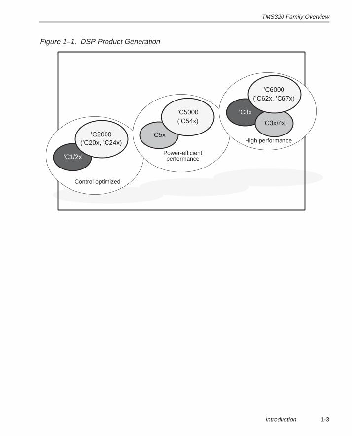
In 1982, Texas Instruments introduced the TMS32010, the first fixed-pointDSP in the TMS320 family. Before the end of the year, Electronic Productsmagazine awarded the TMS32010 the title “Product of the Year”. Today, theTMS320 family consists of the following generations shown in Figure 1–1:’C1x, ’C2x, ’C24x, ’C5x, ’C54x, and ’C6x fixed-point DSPs; ’C3x and ’C4x float-ing-point DSPs; and ’C8x multiprocessor DSPs. The ’C24x is considered partof the ’C24x family of fixed-point DSPs, and a member of the ’C2000 platform.
Devices within a generation of the TMS320 family have the same CPU struc-ture but different on-chip memory and peripheral configurations. Spin-offdevices use new combinations of on-chip memory and peripherals to satisfya wide range of needs in the worldwide electronics market. By integratingmemory and peripherals onto a single chip, TMS320 devices reduce systemcosts and save circuit board space.
TMS320 Family Overview
1-3Introduction
Figure 1–1. DSP Product Generation
Control optimized
’C1/2x
’C2000(’C20x, ’C24x)
performancePower-efficient
’C5xHigh performance
’C8x’C5000(’C54x)
(’C62x, ’C67x)’C6000
’C3x/4x
TMS320 Family Overview
1-4
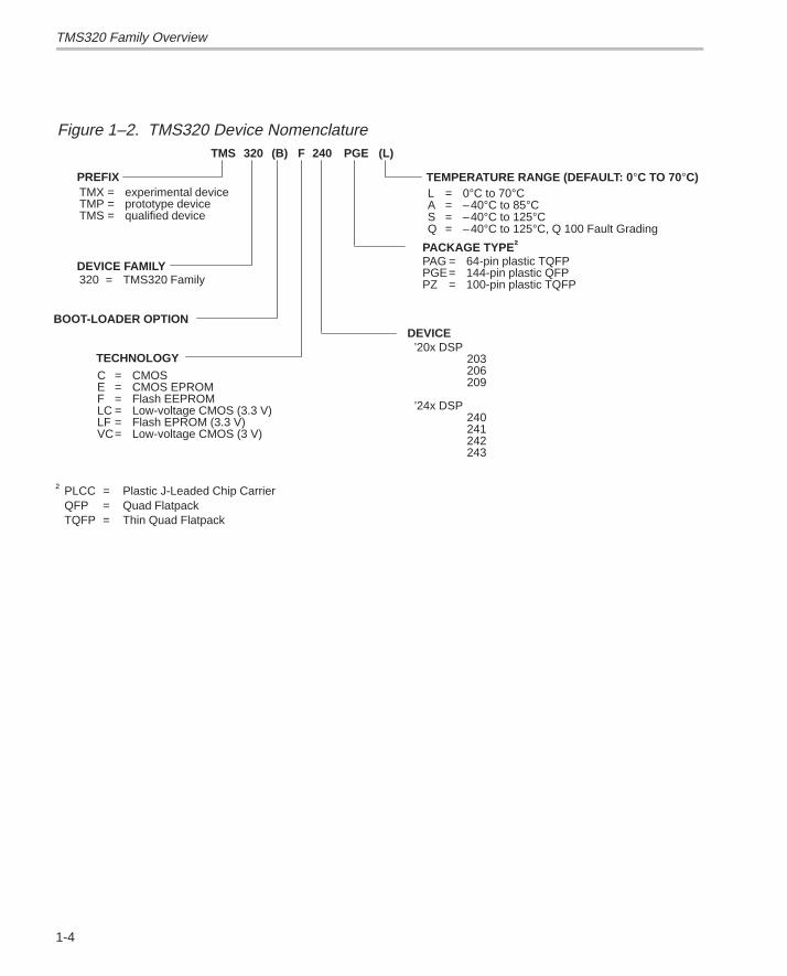
Figure 1–2. TMS320 Device Nomenclature
PREFIX TEMPERATURE RANGE (DEFAULT: 0 °C TO 70°C)
TMS 320 F 240 PGE (L)
TMX = experimental deviceTMP = prototype deviceTMS = qualified device
DEVICE FAMILY320 = TMS320 Family
TECHNOLOGY
L = 0°C to 70°CA = –40°C to 85°CS = –40°C to 125°CQ = –40°C to 125°C, Q 100 Fault Grading
PACKAGE TYPE †PAG = 64-pin plastic TQFPPGE= 144-pin plastic QFPPZ = 100-pin plastic TQFP
C = CMOSE = CMOS EPROMF = Flash EEPROMLC = Low-voltage CMOS (3.3 V)LF = Flash EPROM (3.3 V)VC= Low-voltage CMOS (3 V)
DEVICE’20x DSP
203206209
’24x DSP240241242243
(B)
BOOT-LOADER OPTION
† PLCC = Plastic J-Leaded Chip CarrierQFP = Quad FlatpackTQFP = Thin Quad Flatpack
TMS320C24x Series of DSP Controllers
1-5Introduction
1.2 TMS320C24x Series of DSP Controllers
Designers have recognized the opportunity to redesign existing DMC systemsto use advanced algorithms that yield better performance and reduce systemcomponent count. DSPs enable:
Design of robust controllers for a new generation of inexpensive motors,such as AC induction, DC permanent magnet, and switched-reluctancemotors
Full variable-speed control of brushless motor types that have lowermanufacturing cost and higher reliability
Energy savings through variable-speed control, saving up to 25% of theenergy used by fixed-speed controllers
Increased fuel economy, improved performance, and elimination ofhydraulic fluid in automotive electronic power steering (EPS) systems
Reduced manufacturing and maintenance costs by eliminating hydraulicfluids in automotive electronic braking systems
More efficient and quieter operation due to less generation of torqueripple, resulting in less loss of power, lower vibration, and longer life
Elimination or reduction of memory lookup tables through real-time poly-nomial calculation, thereby reducing system cost
Use of advanced algorithms that can reduce the number of sensorsrequired in a system
Control of power switching inverters, along with control algorithmprocessing
Single-processor control of multimotor systems
The ’C24x DSP controllers are designed to meet the needs of control-basedapplications. By integrating the high performance of a DSP core and theon-chip peripherals of a microcontroller into a single-chip solution, the ’C24xseries yields a device that is an affordable alternative to traditional microcon-troller units (MCUs) and expensive multichip designs. At 20 million instructionsper second (MIPS), the ’C24x DSP controllers offer significant performanceover traditional 16-bit microcontrollers and microprocessors. Future deriva-tives of these devices will run at speeds higher than 20 MIPS.
The 16-bit, fixed-point DSP core of the ’C24x device provides analog design-ers a digital solution that does not sacrifice the precision and performance of
TMS320C24x Series of DSP Controllers
1-6
their systems. In fact, system performance can be enhanced through the useof advanced control algorithms for techniques such as adaptive control,Kalman filtering, and state control. The ’C24x DSP controllers offer reliabilityand programmability. Analog control systems, on the other hand, are hard-wired solutions and can experience performance degradation due to aging,component tolerance, and drift.
The high-speed central processing unit (CPU) allows the digital designer toprocess algorithms in real time rather than approximate results with look-uptables. When the instruction set of these DSP controllers (which incorporatesboth signal processing instructions and general-purpose control functions) iscoupled with the extensive development support available for the ’C24x de-vices, it reduces development time and provides the same ease of use as tra-ditional 8- and 16-bit microcontrollers. The instruction set also allows you toretain your software investment when moving from other general-purposeTMS320 fixed-point DSPs. It is source- and object-code compatible with theother members of the ’C24x generation, source code compatible with the ’C2xgeneration, and upwardly source code compatible with the ’C5x generation ofDSPs from Texas Instruments.
The ’C24x architecture is also well-suited for processing control signals. Ituses a 16-bit word length along with 32-bit registers for storing intermediateresults, and has two hardware shifters available to scale numbers indepen-dently of the CPU. This combination minimizes quantization and truncationerrors, and increases processing power for additional functions. Two exam-ples of these additional functions are: a notch filter that cancels mechanicalresonances in a system, and an estimation technique that eliminates statesensors in a system.
The ’C24x DSP controllers take advantage of an existing set of peripheralfunctions that allow Texas Instruments to quickly configure various seriesmembers for different price/performance points or for application optimization.This library of both digital and mixed-signal peripherals includes:
Timers Serial communications ports (SCI, SPI) Analog-to-digital converters (ADC) Event manager System protection, such as watchdog timers CAN controller
The DSP controller peripheral library is continually growing and changing tosuit the needs of tomorrow’s embedded control marketplace.
2-1Architectural Overview
Architectural Overview
This chapter provides an overview of the architectural structure and compo-nents of the ’C24x DSP CPU. The ’C24x DSP uses an advanced, modifiedHarvard architecture that maximizes processing power by maintaining sepa-rate bus structures for program memory and data memory.
Topic Page
2.1 Architecture Summary 2-2. . . . . . . . . . . . . . . . . . . . . . . . . . . . . . . . . . . . . . . .
2.2 ’C24x CPU Internal Bus Structure 2-4. . . . . . . . . . . . . . . . . . . . . . . . . . . . . .
2.3 Memory 2-5. . . . . . . . . . . . . . . . . . . . . . . . . . . . . . . . . . . . . . . . . . . . . . . . . . . . . .
2.4 Central Processing Unit 2-8. . . . . . . . . . . . . . . . . . . . . . . . . . . . . . . . . . . . . . .
2.5 Program Control 2-10. . . . . . . . . . . . . . . . . . . . . . . . . . . . . . . . . . . . . . . . . . . . .
2.6 Serial-Scan Emulation 2-10. . . . . . . . . . . . . . . . . . . . . . . . . . . . . . . . . . . . . . . .
Chapter 2
Architecture Summary
2-2
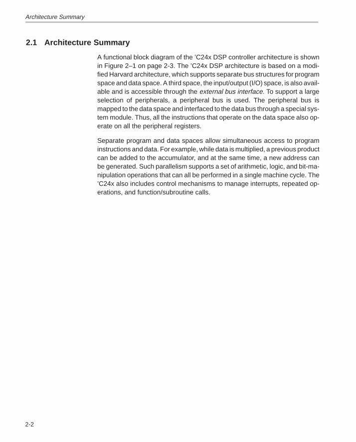
2.1 Architecture Summary
A functional block diagram of the ’C24x DSP controller architecture is shownin Figure 2–1 on page 2-3. The ’C24x DSP architecture is based on a modi-fied Harvard architecture, which supports separate bus structures for programspace and data space. A third space, the input/output (I/O) space, is also avail-able and is accessible through the external bus interface. To support a largeselection of peripherals, a peripheral bus is used. The peripheral bus ismapped to the data space and interfaced to the data bus through a special sys-tem module. Thus, all the instructions that operate on the data space also op-erate on all the peripheral registers.
Separate program and data spaces allow simultaneous access to programinstructions and data. For example, while data is multiplied, a previous productcan be added to the accumulator, and at the same time, a new address canbe generated. Such parallelism supports a set of arithmetic, logic, and bit-ma-nipulation operations that can all be performed in a single machine cycle. The’C24x also includes control mechanisms to manage interrupts, repeated op-erations, and function/subroutine calls.
Architecture Summary
2-3Architectural Overview
Figure 2–1. TMS320C24x DSP Controller Functional Block Diagram
ÁÁÁÁÁÁÁÁÁÁÁÁÁÁÁÁÁÁÁÁÁÁÁÁÁÁÁÁÁÁÁÁÁÁÁÁÁÁÁÁÁÁÁÁÁÁÁÁÁÁÁÁÁÁÁÁÁÁÁÁÁÁÁÁÁÁÁÁÁÁÁÁÁÁÁÁÁÁ
ÁÁÁÁÁÁÁÁÁÁÁÁÁÁÁÁÁÁÁÁÁÁÁÁÁÁÁÁÁÁÁÁÁÁÁÁ
ÁÁÁÁÁÁÁÁÁÁÁÁÁÁÁÁÁÁÁÁÁÁÁÁÁÁÁÁÁÁÁÁÁÁÁÁ
ÁÁÁÁÁÁÁÁÁÁÁÁÁÁÁÁÁÁÁÁÁÁÁÁÁÁÁÁÁÁÁÁÁÁÁÁ
ÁÁÁÁÁÁÁÁÁÁÁÁ
ÁÁÁÁÁÁÁÁÁÁÁÁÁÁÁÁÁÁÁÁÁÁÁÁÁ
ÁÁÁ
24ÁÁÁ
16ÁÁÁÁ
ÁÁ
PDPINTÁÁ
4
ÁÁÁ
ÁÁÁ4
9
ÁÁÁ
Á
ÁÁÁ41
7ÁÁÁÁ
ÁÁ
ÁÁ
ÁÁ
ÁÁ
ÁÁÁÁ
ÁÁÁÁÁÁÁÁÁÁÁÁÁÁÁÁÁÁÁÁÁÁÁÁ
ÁÁÁÁÁÁÁÁÁÁÁÁ
ÁÁÁÁÁÁÁÁÁÁÁÁÁÁÁÁ
ÁÁÁÁÁÁÁÁÁÁÁÁÁÁÁÁ
ÁÁÁÁÁÁÁÁÁÁÁÁÁÁÁÁÁÁÁÁÁÁÁÁ
ÁÁÁÁÁÁÁÁÁÁÁÁÁÁÁÁÁÁÁÁÁÁÁÁ
QuadratureEncoder
Pulse (QEP)
Capture/
UnitsCompare
TimersPurposeGeneral-
ManagerEvent
Generator
Wait-StateSoftware
InterfaceMemoryExternal
EmulationJTAG Test/
Peripheral Bus
ÁÁÁ
ÁÁÁ
ÁÁÁ
ÁÁÁÁÁÁ
ÁÁÁÁÁÁÁÁÁÁÁÁÁÁÁÁÁÁÁÁ
ÁÁÁÁÁÁÁÁÁÁÁÁÁÁÁÁÁÁÁÁÁÁÁÁÁÁÁÁ
ÁÁÁÁÁÁÁÁÁÁÁÁÁÁÁÁÁÁÁÁ
ÁÁÁÁÁÁÁÁÁÁÁÁÁÁÁÁÁÁÁÁ
TimerWatchdog
InterfaceCommunications
Serial-
InterfacePeripheral
Serial-
Converterto-DigitalAnalog-10–Bit
Data Bus
ÁÁÁ
ÁÁÁ
Á3
Á
Á
Reset
Digital Input/Output
Interrupts20
4
ÁÁÁÁÁÁ
Á
ÁÁÁ
ÁÁÁÁ
ÁÁÁÁÁÁÁÁÁÁÁÁÁÁÁÁÁÁÁÁÁÁÁÁÁÁÁÁÁÁÁÁÁÁÁÁ
ÁÁÁÁÁÁÁÁÁÁÁÁÁÁÁÁ
ModuleSystem-Interface
ModuleClock
Program Bus
ÁÁÁÁ
ÁÁ
ÁÁÁÁÁÁ
ÁÁÁÁÁÁÁÁÁÁ
ÁÁÁÁÁÁÁÁÁÁ
ÁÁÁÁÁÁÁÁÁÁ
B1/B2DARAM
B0DARAMROM or Flash
EEPROM†
Initialization
Interrupts
ControlMemory
ÁÁ
ÁÁ
ÁÁÁÁ
ÁÁÁ
ÁÁ
Á
ControllerProgram
CPU’C2xx
ÁÁÁÁÁÁÁÁÁÁÁÁ
ÁÁÁÁ
ÁÁ
ShifterProduct
PREG
TREG
Multiplier
ShifterOutput
Accumulator
ALU
ShifterInput
RegistersMapped
Memory-
RegistersAuxiliary
RegistersControlStatus/
ARAU
RegisterInstruction
Á
ÁÁ
† ’C24x devices contains ROM: ’F24x
devices contains Flash EEPROM.
WatchdogÁÁÁÁÁÁÁÁÁÁÁÁÁÁÁÁÁÁÁÁ
ÁÁ
ÁÁ
1 2Á Á
ÁÁÁÁCAN
ÁÁNote: The number ofPWMS/digital I/O, ADCchannels, and peripheralmodules are dependentupon the device family.
’C24x CPU Internal Bus Structure
2-4
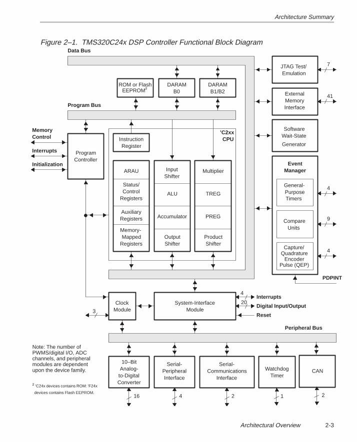
2.2 ’C24x CPU Internal Bus Structure
The ’C24x DSP, a member of the TMS320 family of DSPs, includes a ’C2xxDSP core designed using the ’2xLP ASIC core. The ’C2xx DSP core has aninternal data and program bus structure that is divided into six 16-bit buses(see Figure 2–2). The six buses are:
PAB. The program address bus provides addresses for both reads fromand writes to program memory.
DRAB. The data-read address bus provides addresses for reads fromdata memory.
DWAB. The data-write address bus provides addresses for writes to datamemory.
PRDB. The program read bus carries instruction code and immediate op-erands, as well as table information, from program memory to the CPU.
DRDB. The data-read bus carries data from data memory to the centralarithmetic logic unit (CALU) and the auxiliary register arithmetic unit(ARAU).
DWEB. The data-write bus carries data to both program memory and datamemory.
Having separate address buses for data reads (DRAB) and data writes(DWAB) allows the CPU to read and write in the same machine cycle.
Figure 2–2. ’C24x Address and Data Bus Structure
B0DARAM
Flash/ROM
B1, B2DARAM
Memory-mappedregisters
PAB
DRAB
DWAB
PRDB
DRDB
DWEB
Central processing unit (CPU)
Externaladdress bus
Externaldata bus
System moduleExternal businterface
Memory
2-5Architectural Overview
2.3 Memory
The ’C24x contains the following types of on-chip memory:
Dual-access RAM (DARAM) Flash EEPROM or ROM (masked)
The ’C24x memory is organized into four individually-selectable spaces:
Program (64K words) Local data (64K words) Global data (32K words) Input/Output (64K words)
These spaces form an address range of 224K words.
2.3.1 On-Chip Dual-Access RAM (DARAM)
The ’C24x has 544 words of on-chip DARAM, which can be accessed twiceper machine cycle. This memory is primarily intended to hold data, but whenneeded, can also be used to hold programs. The memory can be configuredin one of two ways, depending on the state of the CNF bit in status register ST1.
When CNF = 0, all 544 words are configured as data memory.
When CNF = 1, 288 words are configured as data memory and 256 wordsare configured as program memory.
Because DARAM can be accessed twice per cycle, it improves the speed ofthe CPU. The CPU operates within a 4-cycle pipeline. In this pipeline, the CPUreads data on the third cycle and writes data on the fourth cycle. However, DARAM allows the CPU to write and read in one cycle; the CPU writes toDARAM on the master phase of the cycle and reads from DARAM on the slavephase. For example, suppose two instructions, A and B, store the accumulatorvalue to DARAM and load the accumulator with a new value from DARAM.Instruction A stores the accumulator value during the master phase of the CPUcycle, and instruction B loads the new value in the accumulator during theslave phase. Because part of the dual-access operation is a write, it onlyapplies to RAM.
Memory
2-6
2.3.2 Flash EEPROM
Flash EEPROM provides an attractive alternative to masked program ROM.Like ROM, flash is a nonvolatile memory type; however, it has the advantageof in-target reprogrammability. The ’F24x incorporates one 16K/8K × 16-bitflash EEPROM module in program space. This type of memory expands thecapabilities of the ’F24x in the areas of prototyping, early field testing, andsingle-chip applications.
Unlike most discrete flash memory, the ’F24x flash does not require a dedi-cated state machine because the algorithms for programming and erasing theflash are executed by the DSP core. This enables several advantages, includ-ing reduced chip size and sophisticated adaptive algorithms. For productionprogramming, the IEEE Standard 1149.1 (JTAG) scan port provides easy ac-cess to on-chip RAM for downloading the algorithms and flash code. Other keyfeatures of the flash include zero-wait-state access rate and single 5-V powersupply.
An erased bit in the ’24x flash is read as a logic one, and a programmed bit isread as a logic zero. The flash requires a block-erase of the entire 16K/8Kmodule; however, any combination of bits can be programmed. The followingfour algorithms are required for flash operations: clear, erase, flash-write, andprogram. For an explanation of these algorithms and a complete descriptionof the flash EEPROM, see TMS320F20x/F24x DSPs Embedded FlashMemory Technical Reference (Literature number SPRU282).
2.3.3 Flash Serial Loader
Most of the on-chip flash devices are shipped with a serial bootloader codeprogrammed at the following addresses: 0x0000 – 0x00FFh. All other flash ad-dresses are in an erased state. The serial bootloader can be used to programthe on-chip flash memory with user’s code. During the flash programming se-quence, the on-chip data RAM is used to load and execute the clear, erase,and program algorithms.
2.3.4 Factory-Masked ROM
For large-volume applications consisting of stable software free of bugs, low-cost, masked ROM is available and supported up to 16K or 4K words. If youwant a custom ROM, you can provide the code or data to be programmed intothe ROM in object-file format, and Texas Instruments will generate the ap-propriate process mask to program the ROM. For details, see Appendix B,Submitting ROM Codes to TI.
A small portion of the ROM (128 or 64 words) is reserved by Texas Instrumentsfor test purposes. These reserved locations are at addresses 0x3F80 or 3FC0through 0x3FFF. This leaves about 16K words available for your code.
Memory
2-7Architectural Overview
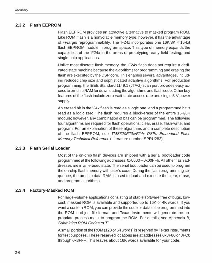
Figure 2–3. ’C24x ROM Memory Map
3FFF
for codeAvailable
3F80/3FC0
3F7F
0000
Reservedfor test
2.3.5 External Memory Interface Module
In addition to full, on-chip memory support, some of the ’C24x devices provideaccess to external memory by way of the External Memory Interface Module.This interface provides 16 external address lines, 16 external data lines, andrelevant control signals to select data, program, and I/O spaces. An on-chipwait-state generator allows interfacing with slower off-chip memory and pe-ripherals.
Central Processing Unit
2-8
2.4 Central Processing Unit
The ’C24x is based on TI’s ’C2xx CPU. It contains:
A 32-bit central arithmetic logic unit (CALU) A 32-bit accumulator Input and output data-scaling shifters for the CALU A 16-bit × 16-bit multiplier A product-scaling shifter Data-address generation logic, which includes eight auxiliary registers
and an auxiliary register arithmetic unit (ARAU) Program-address generation logic
2.4.1 Central Arithmetic Logic Unit (CALU) and Accumulator
The ’C24x performs 2s-complement arithmetic using the 32-bit CALU. TheCALU uses 16-bit words taken from data memory, derived from an immediateinstruction, or from the 32-bit multiplier result. In addition to arithmetic opera-tions, the CALU can perform Boolean operations.
The accumulator stores the output from the CALU; it can also provide a secondinput to the CALU. The accumulator is 32 bits wide and is divided into a high-order word (bits 31 through 16) and a low-order word (bits 15 through 0).Assembly language instructions are provided for storing the high- and low-order accumulator words to data memory.
2.4.2 Scaling Shifters
The ’C24x has three 32-bit shifters that allow for scaling, bit extraction,extended arithmetic, and overflow-prevention operations:
Input data-scaling shifter (input shifter). This shifter left-shifts 16-bit in-put data by 0 to 16 bits to align the data to the 32-bit input of the CALU.
Output data-scaling shifter (output shifter). This shifter left-shift outputfrom the accumulator by 0 to 7 bits before the output is stored to datamemory. The content of the accumulator remains unchanged.
Product-scaling shifter (product shifter) . The product register (PREG)receives the output of the multiplier. The product shifter shifts the outputof the PREG before that output is sent to the input of the CALU. The prod-uct shifter has four product shift modes (no shift, left shift by one bit, leftshift by four bits, and right shift by six bits), which are useful for performingmultiply/accumulate operations, performing fractional arithmetic, or justi-fying fractional products.
Central Processing Unit
2-9Architectural Overview
2.4.3 Multiplier
The on-chip multiplier performs 16-bit × 16-bit 2s-complement multiplicationwith a 32-bit result. In conjunction with the multiplier, the ’C24x uses the 16-bittemporary register (TREG) and the 32-bit product register (PREG); TREG al-ways supplies one of the values to be multiplied, and PREG receives the resultof each multiplication.
Using the multiplier, TREG, and PREG, the ’C24x efficiently performs funda-mental DSP operations such as convolution, correlation, and filtering. The ef-fective execution time of each multiplication instruction can be as short as oneCPU cycle.
2.4.4 Auxiliary Register Arithmetic Unit (ARAU) and Auxiliary Registers
The ARAU generates data memory addresses when an instruction uses indi-rect addressing (see Chapter 6, Addressing Modes) to access data memory.The ARAU is supported by eight auxiliary registers (AR0 through AR7), eachof which can be loaded with a 16-bit value from data memory or directly froman instruction word. Each auxiliary register value can also be stored in datamemory. The auxiliary registers are referenced by a 3-bit auxiliary registerpointer (ARP) embedded in status register ST0.
Program Control
2-10
2.5 Program Control
Several hardware and software mechanisms provide program control:
Program control logic decodes instructions, manages the 4-level pipeline,stores the status of operations, and decodes conditional operations. Hard-ware elements included in the program control logic are the programcounter, the status registers, the stack, and the address-generation logic.
Software mechanisms used for program control include branches, calls,conditional instructions, a repeat instruction, reset, interrupts, and power-down modes.
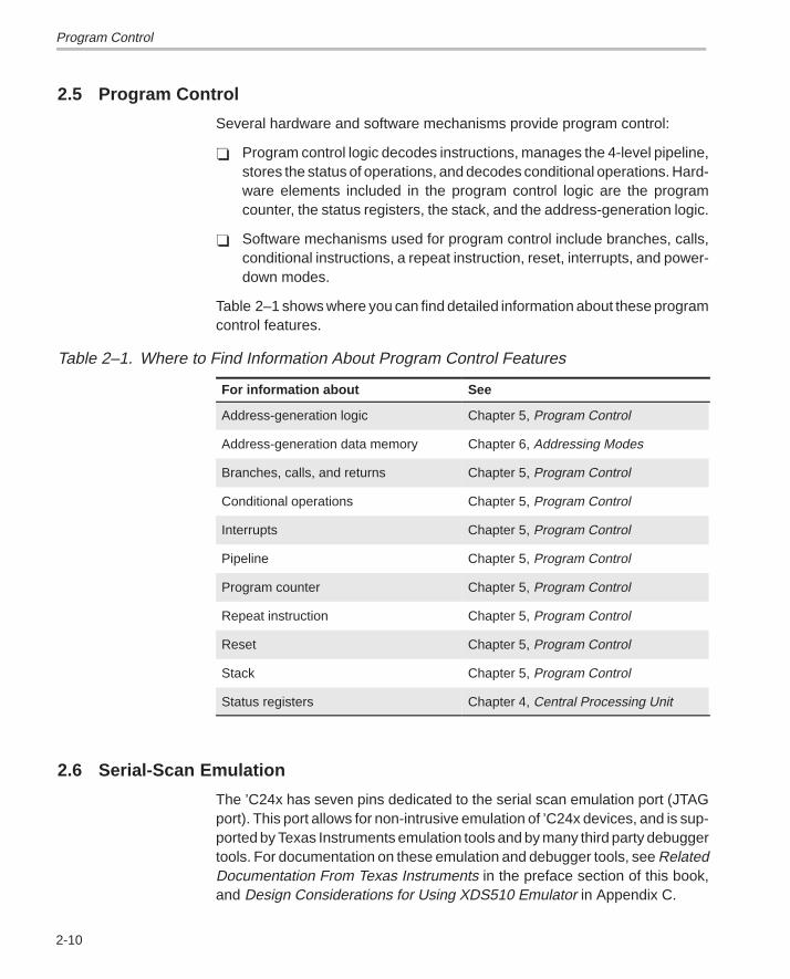
Table 2–1 shows where you can find detailed information about these programcontrol features.
Table 2–1. Where to Find Information About Program Control Features
For information about See
Address-generation logic Chapter 5, Program Control
Address-generation data memory Chapter 6, Addressing Modes
Branches, calls, and returns Chapter 5, Program Control
Conditional operations Chapter 5, Program Control
Interrupts Chapter 5, Program Control
Pipeline Chapter 5, Program Control
Program counter Chapter 5, Program Control
Repeat instruction Chapter 5, Program Control
Reset Chapter 5, Program Control
Stack Chapter 5, Program Control
Status registers Chapter 4, Central Processing Unit
2.6 Serial-Scan Emulation
The ’C24x has seven pins dedicated to the serial scan emulation port (JTAGport). This port allows for non-intrusive emulation of ’C24x devices, and is sup-ported by Texas Instruments emulation tools and by many third party debuggertools. For documentation on these emulation and debugger tools, see RelatedDocumentation From Texas Instruments in the preface section of this book,and Design Considerations for Using XDS510 Emulator in Appendix C.
3-1Memory and I/O Spaces
Memory and I/O Spaces
The ’C24x has a 16-bit address line that accesses four individually selectablespaces (224K words total):
A 64K-word program space A 64K-word local data space A 32K-word global data space A 64K-word I/O space
This chapter describes these four spaces and shows memory maps for pro-gram, data, and I/O spaces. It also describes available ’C24x memory configuration options.
Topic Page
3.1 Overview of Memory and I/O Spaces 3-2. . . . . . . . . . . . . . . . . . . . . . . . . . . .
3.2 Program Memory 3-4. . . . . . . . . . . . . . . . . . . . . . . . . . . . . . . . . . . . . . . . . . . . .
3.3 Data Memory 3-6. . . . . . . . . . . . . . . . . . . . . . . . . . . . . . . . . . . . . . . . . . . . . . . . .
3.4 Global Data Memory 3-9. . . . . . . . . . . . . . . . . . . . . . . . . . . . . . . . . . . . . . . . . . .
3.5 I/O Space 3-11. . . . . . . . . . . . . . . . . . . . . . . . . . . . . . . . . . . . . . . . . . . . . . . . . . . .
Chapter 3
Overview of Memory and I/O Spaces
3-2
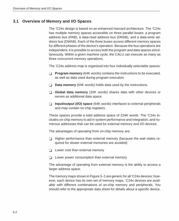
3.1 Overview of Memory and I/O Spaces
The ’C24x design is based on an enhanced Harvard architecture. The ’C24xhas multiple memory spaces accessible on three parallel buses: a programaddress bus (PAB), a data-read address bus (DRAB), and a data-write ad-dress bus (DWAB). Each of the three buses access different memory spacesfor different phases of the device’s operation. Because the bus operations areindependent, it is possible to access both the program and data spaces simul-taneously. Within a given machine cycle, the CALU can execute as many asthree concurrent memory operations.
The ’C24x address map is organized into four individually selectable spaces:
Program memory (64K words) contains the instructions to be executed,as well as data used during program execution.
Data memory (64K words) holds data used by the instructions.
Global data memory (32K words) shares data with other devices orserves as additional data space.
Input/output (I/O) space (64K words) interfaces to external peripheralsand may contain on-chip registers.
These spaces provide a total address space of 224K words. The ’C24x in-cludes on-chip memory to aid in system performance and integration, and nu-merous addresses that can be used for external memory and I/O devices.
The advantages of operating from on-chip memory are:
Higher performance than external memory (because the wait states re-quired for slower external memories are avoided)
Lower cost than external memory
Lower power consumption than external memory
The advantage of operating from external memory is the ability to access alarger address space.
The memory maps shown in Figure 3–1 are generic for all ’C24x devices; how-ever, each device has its own set of memory maps. ’C24x devices are avail-able with different combinations of on-chip memory and peripherals. Youshould refer to the appropriate data sheet for details about a specific device.
Overview of Memory and I/O Spaces
3-3Memory and I/O Spaces
Figure 3–1. Generic Memory Maps for ’C24x DSP Controllers
ÄÄÄÄÄÄÄÄÄÄÄÄÄÄÄÄÄÄÄÄÄ
ÄÄÄÄÄÄÄÄÄÄÄÄÄÄÄÄÄÄÄÄÄ
Reserved/illegal
ÂÂÂÂÂÂÂÂÂÂÂÂÂÂÂÂÂÂÂÂÂÂÂÂ
ÂÂÂÂÂÂÂÂÂÂÂÂ
Reserved/illegal
Reserved/illegal
ÂÂÂÂÂÂÂÂÂÂÂÂ
0000
005F0060
01FF
02FF0300
0200
03FF0400
7000 Peripheral memory-mapped registers(system,WD, ADC,SCI, SPI, CAN, I/O,
interrupts)73FF7400
743F7440
DataHex
007F0080
8000
External
FFFF
7FFF
Memory-mappedregisters/reserved
addresses
On-chipDARAM B2
On-chip DARAM(B0)‡ (CNF = 0)
reserved (CNF = 1)
On-chipDARAM (B1) §
6FFF
Peripheralmemory-mapped
registers(event manager)
0000
003F0040
FEFF
FDFFFE00
Hex
External
On-chip DARAM(B0)† (CNF = 1)
external (CNF = 0)
Program
FF00
FFFF
Illegal
Interruptvectors
Reserved †
(CNF = 1)external (CNF = 0)
On-chipFlash/ROM
0000
External
FF0E
I/OHex
FFFFWait-state generator
control register(on-chip)
Flash controlmode register
Reserved
FEFFFF00
FF10
FFFE
FF0F
On-chip FLASH memory, (16K or 8K) if MP/MC = 0external program memory, if MP/MC = 1
3FFF or 1FFF
4000 or 2000
† When CNF = 1, addresses FE00h–FEFFh and FF00h–FFFFh are mapped to the same physical block (B0) in program-memoryspace. For example, a write to FE00h will have the same effect as a write to FF00h. For simplicity, addresses FE00h–FEFFhare referred to as reserved when CNF = 1.
‡ When CNF = 0, addresses 0100h–01FFh and 0200h–02FFh are mapped to the same physical block (B0) in data-memoryspace. For example, a write to 0100h will have the same effect as a write to 0200h. For simplicity, addresses 0100h–01FFh arereferred to as reserved.
§ Addresses 0300h–03FFh and 0400h–04FFh are mapped to the same physical block (B1) in data-memory space. For example,a write to 0400h has the same effect as a write to 0300h. For simplicity, addresses 0400h–04FFh are referred to as reserved.
Program Memory
3-4
3.2 Program Memory
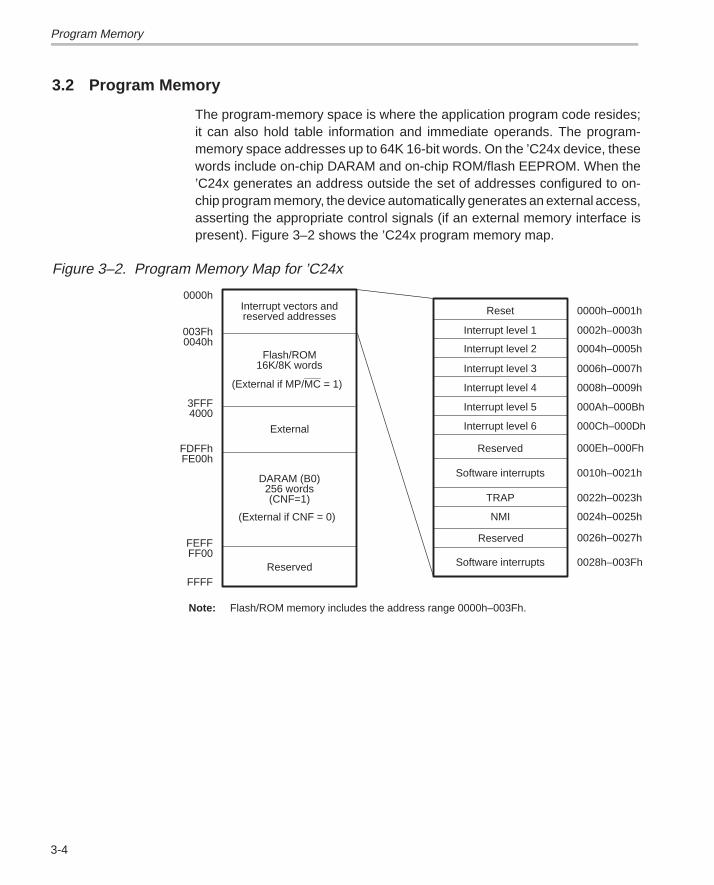
The program-memory space is where the application program code resides;it can also hold table information and immediate operands. The program-memory space addresses up to 64K 16-bit words. On the ’C24x device, thesewords include on-chip DARAM and on-chip ROM/flash EEPROM. When the’C24x generates an address outside the set of addresses configured to on-chip program memory, the device automatically generates an external access,asserting the appropriate control signals (if an external memory interface ispresent). Figure 3–2 shows the ’C24x program memory map.
Figure 3–2. Program Memory Map for ’C24x
0000h
003Fh0040h
FDFFhFE00h
FFFF
0000h–0001h
0002h–0003h
0004h–0005h
0006h–0007h
0008h–0009h
000Ah–000Bh
000Ch–000Dh
000Eh–000Fh
0022h–0023h
0024h–0025h
Interrupt vectors and
Flash/ROM16K/8K words
External
DARAM (B0)256 words
Reset
Interrupt level 1
Interrupt level 2
Interrupt level 3
Interrupt level 4
Interrupt level 5
Interrupt level 6
TRAP
NMI
(CNF=1)
0010h–0021hSoftware interrupts
Software interrupts 0028h–003Fh
Reserved
Reserved 0026h–0027h
reserved addresses
(External if MP/MC = 1)
(External if CNF = 0)
Note: Flash/ROM memory includes the address range 0000h–003Fh.
3FFF4000
FEFFFF00
Reserved
Program Memory
3-5Memory and I/O Spaces
3.2.1 Program Memory Configuration
Depending on which types of memory are included in a particular ’C24x de-vice, two factors contribute to the configuration of program memory:
CNF bit. The CNF bit (bit 12) of status register ST1 determines whetherthe addresses for DARAM B0 are available for program space:
CNF = 0. There is no addressable on-chip program DARAM.
CNF = 1. The 256 words of DARAM B0 are configured for programuse. At reset, any words of program/data DARAM are mapped into lo-cal data space (CNF = 0).
MP/MC pin. The level on the MP/MC pin determines whether programinstructions are read from on-chip ROM or flash EEPROM (if available) af-ter reset:
MP/MC = 0. The device is configured as a microcomputer. The on-chip ROM/flash EEPROM is accessible. The device fetches the resetvector from on-chip memory.
MP/MC = 1. The device is configured as a microprocessor. The devicefetches the reset vector from external memory.
Regardless of the value of MP/MC, the ’C24x fetches its reset vector atlocation 0000h of program memory.
Data Memory
3-6
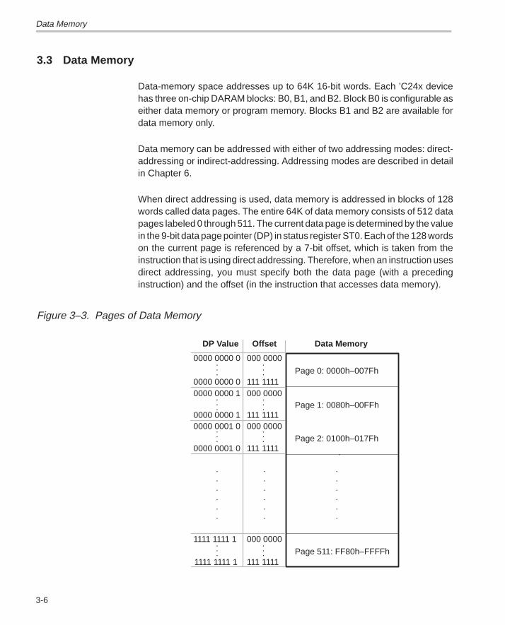
3.3 Data Memory
Data-memory space addresses up to 64K 16-bit words. Each ’C24x devicehas three on-chip DARAM blocks: B0, B1, and B2. Block B0 is configurable aseither data memory or program memory. Blocks B1 and B2 are available fordata memory only.
Data memory can be addressed with either of two addressing modes: direct-addressing or indirect-addressing. Addressing modes are described in detailin Chapter 6.
When direct addressing is used, data memory is addressed in blocks of 128words called data pages. The entire 64K of data memory consists of 512 datapages labeled 0 through 511. The current data page is determined by the valuein the 9-bit data page pointer (DP) in status register ST0. Each of the 128 wordson the current page is referenced by a 7-bit offset, which is taken from theinstruction that is using direct addressing. Therefore, when an instruction usesdirect addressing, you must specify both the data page (with a precedinginstruction) and the offset (in the instruction that accesses data memory).
Figure 3–3. Pages of Data Memory
Data Memory
Page 0: 0000h–007Fh
Page 1: 0080h–00FFh
Page 2: 0100h–017Fh
Page 511: FF80h–FFFFh
.
000 0000
OffsetDP Value
0000 0000 0
111 11110000 0000 00000 0000 1
0000 0000 1
1111 1111 1
1111 1111 1
000 0000
111 1111
000 0000
111 1111
0000 0001 0
000 0000
111 1111
.
.
.
.
.
.
.
.
.
.
.
.
.
.
.
.
.
.
..
.0000 0001 0
..
.
..
. ...
..
.
..
.
..
. ...
Data Memory
3-7Memory and I/O Spaces
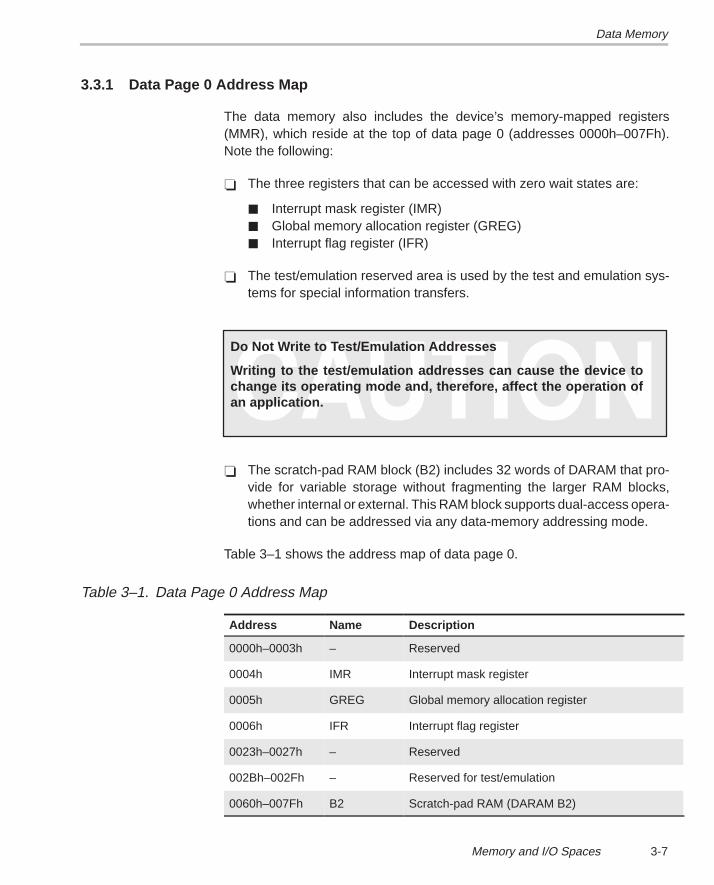
3.3.1 Data Page 0 Address Map
The data memory also includes the device’s memory-mapped registers(MMR), which reside at the top of data page 0 (addresses 0000h–007Fh).Note the following:
The three registers that can be accessed with zero wait states are:
Interrupt mask register (IMR) Global memory allocation register (GREG) Interrupt flag register (IFR)
The test/emulation reserved area is used by the test and emulation sys-tems for special information transfers.
Do Not Write to Test/Emulation Addresses
Writing to the test/emulation addresses can cause the device tochange its operating mode and, therefore, affect the operation ofan application.
The scratch-pad RAM block (B2) includes 32 words of DARAM that pro-vide for variable storage without fragmenting the larger RAM blocks,whether internal or external. This RAM block supports dual-access opera-tions and can be addressed via any data-memory addressing mode.
Table 3–1 shows the address map of data page 0.
Table 3–1. Data Page 0 Address Map
Address Name Description
0000h–0003h – Reserved
0004h IMR Interrupt mask register
0005h GREG Global memory allocation register
0006h IFR Interrupt flag register
0023h–0027h – Reserved
002Bh–002Fh – Reserved for test/emulation
0060h–007Fh B2 Scratch-pad RAM (DARAM B2)
Data Memory
3-8
3.3.2 Data Memory Configuration
The following contributes to the configuration of data memory:
CNF bit. The CNF bit (bit 12) of status register ST1 determines whetherthe on-chip DARAM B0 is mapped into local data space or into programspace.
CNF = 1. DARAM B0 is used for program space.
CNF = 0. B0 is used for data space.
At reset, B0 is mapped into local data space (CNF = 0).
Global Data Memory
3-9Memory and I/O Spaces
3.4 Global Data Memory
Addresses in the upper 32K words (8000h–FFFFh) of local data memory canbe used for global data memory. The global memory allocation register(GREG) determines the size of the global data-memory space, which is be-tween 256 and 32K words. The GREG is connected to the eight LSBs of theinternal data bus and is memory-mapped to data-memory location 0005h.Table 3–2 shows the allowable GREG values and shows the correspondingaddress range set aside for global data memory. Any remaining addresseswithin 8000h–FFFFh are available for local data memory.
Note:
Choose only the GREG values listed in Table 3–2. Other values lead to frag-mented memory maps.
Table 3–2. Global Data Memory Configurations
GREG Value Local Memory Global Memory
High Byte Low Byte Range Words Range Words
XXXX XXXX 0000 0000 0000h–FFFFh 65536 – 0
XXXX XXXX 1000 0000 0000h–7FFFh 32768 8000h–FFFFh 32768
XXXX XXXX 1100 0000 0000h–BFFFh 49152 C000h–FFFFh 16384
XXXX XXXX 1110 0000 0000h–DFFFh 57344 E000h–FFFFh 8192
XXXX XXXX 1111 0000 0000h–EFFFh 61440 F000h–FFFFh 4096
XXXX XXXX 1111 1000 0000h–F7FFh 63488 F800h–FFFFh 2048
XXXX XXXX 1111 1100 0000h–FBFFh 64512 FC00h–FFFFh 1024
XXXX XXXX 1111 1110 0000h–FDFFh 65024 FE00h–FFFFh 512
XXXX XXXX 1111 1111 0000h–FEFFh 65280 FF00h–FFFFh 256
Note: X = Don’t care
When a program accesses any data address, the ’C24x drives the DS signallow. If that address is within the range defined by the GREG as a global ad-dress, BR signal is also asserted. Because BR differentiates local and globalaccesses, the addresses configured by the GREG value are an additional dataspace. The external data-address range is extended by the selected amountof global space (up to 32K words).
Global memory is available only on devices with an external memory interface.In other devices, this space and the GREG register are reserved.
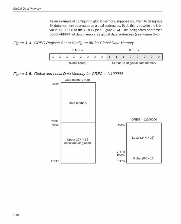
Global Data Memory
3-10
As an example of configuring global memory, suppose you want to designate8K data-memory addresses as global addresses. To do this, you write the 8-bitvalue 11100000 to the GREG (see Figure 3–4). This designates addressesE000h–FFFFh of data memory as global data addresses (see Figure 3–5).
Figure 3–4. GREG Register Set to Configure 8K for Global Data Memory
8 MSBs 8 LSBs
X X X X X X X X 1 1 1 0 0 0 0 0
(Don’t cares) Set for 8K of global data memory
Figure 3–5. Global and Local Data Memory for GREG = 11100000
Data memory map
FFFFh
8000h
0000h
Upper 32K × 16(local and/or global)
7FFFh
Data memory
GREG = 11100000
Global (8K × 16)
Local (24K × 16)
E000hDFFFh
8000h
FFFFh
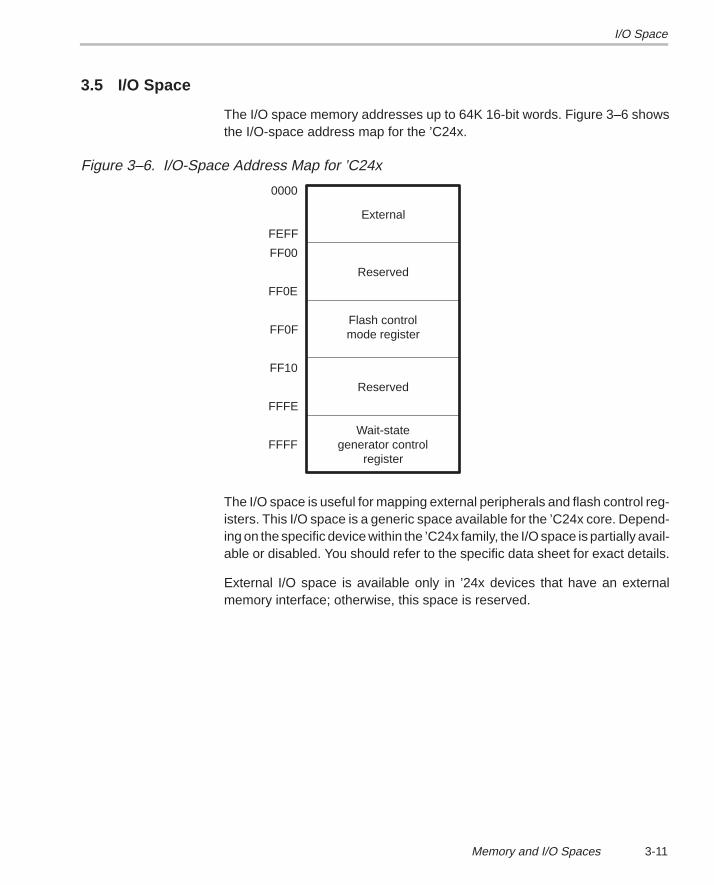
I/O Space
3-11Memory and I/O Spaces
3.5 I/O Space
The I/O space memory addresses up to 64K 16-bit words. Figure 3–6 showsthe I/O-space address map for the ’C24x.
Figure 3–6. I/O-Space Address Map for ’C24x
FFFF
FFFE
FF10
FF0F
FF0E
FF00
FEFF
0000
registergenerator control
Wait-state
Reserved
mode registerFlash control
Reserved
External
The I/O space is useful for mapping external peripherals and flash control reg-isters. This I/O space is a generic space available for the ’C24x core. Depend-ing on the specific device within the ’C24x family, the I/O space is partially avail-able or disabled. You should refer to the specific data sheet for exact details.
External I/O space is available only in ’24x devices that have an externalmemory interface; otherwise, this space is reserved.
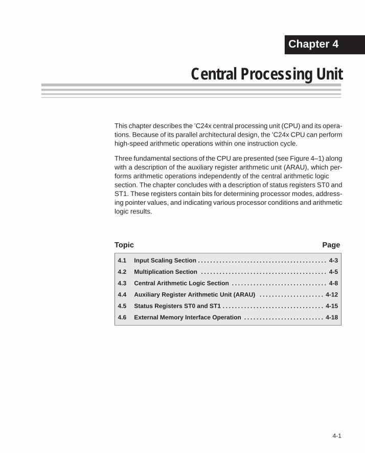
4-1
Central Processing Unit
This chapter describes the ’C24x central processing unit (CPU) and its opera-tions. Because of its parallel architectural design, the ’C24x CPU can performhigh-speed arithmetic operations within one instruction cycle.
Three fundamental sections of the CPU are presented (see Figure 4–1) alongwith a description of the auxiliary register arithmetic unit (ARAU), which per-forms arithmetic operations independently of the central arithmetic logic section. The chapter concludes with a description of status registers ST0 andST1. These registers contain bits for determining processor modes, address-ing pointer values, and indicating various processor conditions and arithmeticlogic results.
Topic Page
4.1 Input Scaling Section 4-3. . . . . . . . . . . . . . . . . . . . . . . . . . . . . . . . . . . . . . . . . .
4.2 Multiplication Section 4-5. . . . . . . . . . . . . . . . . . . . . . . . . . . . . . . . . . . . . . . . .
4.3 Central Arithmetic Logic Section 4-8. . . . . . . . . . . . . . . . . . . . . . . . . . . . . . .
4.4 Auxiliary Register Arithmetic Unit (ARAU) 4-12. . . . . . . . . . . . . . . . . . . . .
4.5 Status Registers ST0 and ST1 4-15. . . . . . . . . . . . . . . . . . . . . . . . . . . . . . . . .
4.6 External Memory Interface Operation 4-18. . . . . . . . . . . . . . . . . . . . . . . . . .
Chapter 4
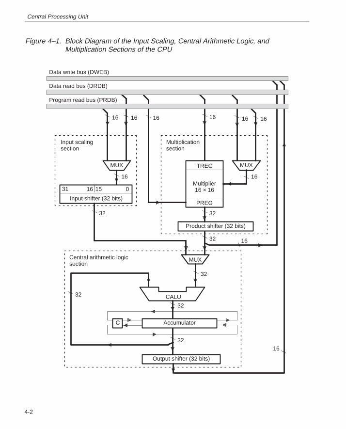
4-2
Figure 4–1. Block Diagram of the Input Scaling, Central Arithmetic Logic, andMultiplication Sections of the CPU
32
Input shifter (32 bits)
16
32
Output shifter (32 bits)
32
C Accumulator
CALU
32
32
MUX
32
16
MUX MUX
16 16
PREG
Multiplier16 × 16
16
Data write bus (DWEB)
Data read bus (DRDB)
TREG
1616
Program read bus (PRDB)
16
16
Product shifter (32 bits)
16
Central arithmetic logicsection
Multiplicationsection
31 016 15
32
Input scalingsection
Central Processing Unit
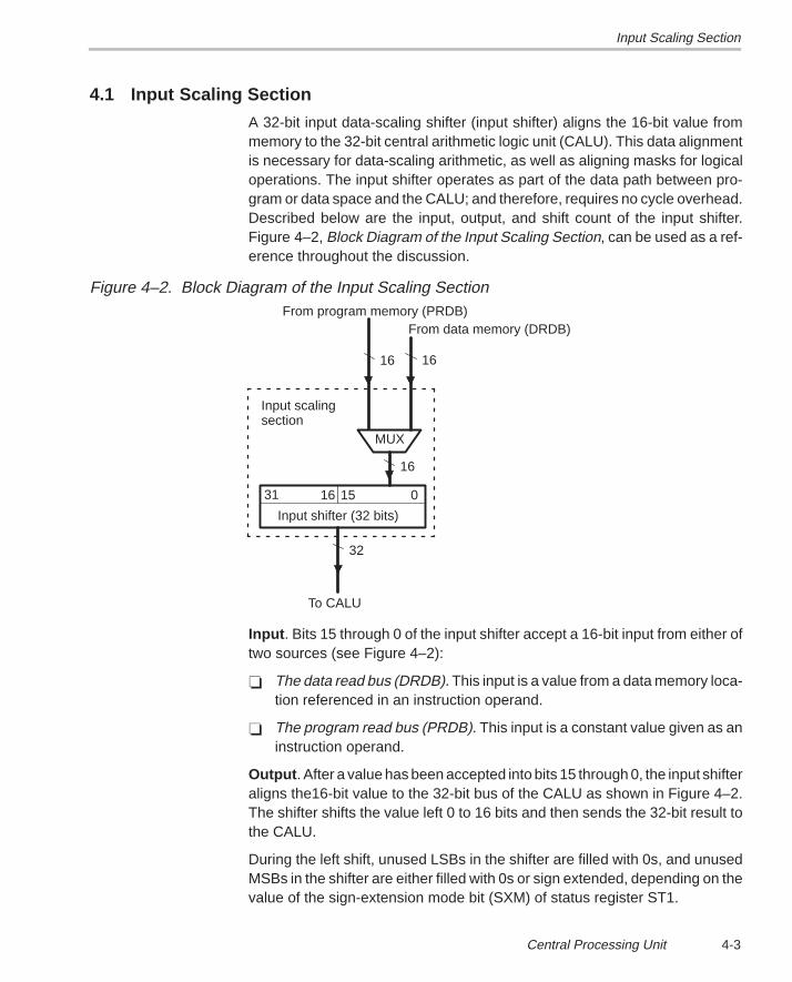
Input Scaling Section
4-3Central Processing Unit
4.1 Input Scaling Section
A 32-bit input data-scaling shifter (input shifter) aligns the 16-bit value frommemory to the 32-bit central arithmetic logic unit (CALU). This data alignmentis necessary for data-scaling arithmetic, as well as aligning masks for logicaloperations. The input shifter operates as part of the data path between pro-gram or data space and the CALU; and therefore, requires no cycle overhead.Described below are the input, output, and shift count of the input shifter.Figure 4–2, Block Diagram of the Input Scaling Section, can be used as a ref-erence throughout the discussion.
Figure 4–2. Block Diagram of the Input Scaling Section
Input shifter (32 bits)
16
32
16
MUX
31 016 15
Input scalingsection
16
From data memory (DRDB)From program memory (PRDB)
To CALU
Input . Bits 15 through 0 of the input shifter accept a 16-bit input from either oftwo sources (see Figure 4–2):
The data read bus (DRDB). This input is a value from a data memory loca-tion referenced in an instruction operand.
The program read bus (PRDB). This input is a constant value given as aninstruction operand.
Output . After a value has been accepted into bits 15 through 0, the input shifteraligns the16-bit value to the 32-bit bus of the CALU as shown in Figure 4–2.The shifter shifts the value left 0 to 16 bits and then sends the 32-bit result tothe CALU.
During the left shift, unused LSBs in the shifter are filled with 0s, and unusedMSBs in the shifter are either filled with 0s or sign extended, depending on thevalue of the sign-extension mode bit (SXM) of status register ST1.
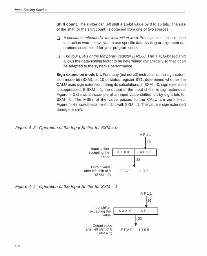
Input Scaling Section
4-4
Shift count . The shifter can left shift a 16-bit value by 0 to 16 bits. The sizeof the shift (or the shift count) is obtained from one of two sources:
A constant embedded in the instruction word. Putting the shift count in theinstruction word allows you to use specific data-scaling or alignment op-erations customized for your program code.
The four LSBs of the temporary register (TREG). The TREG-based shiftallows the data-scaling factor to be determined dynamically so that it canbe adapted to the system’s performance.
Sign-extension mode bit. For many (but not all) instructions, the sign-exten-sion mode bit (SXM), bit 10 of status register ST1, determines whether theCALU uses sign extension during its calculations. If SXM = 0, sign extensionis suppressed. If SXM = 1, the output of the input shifter is sign extended.Figure 4–3 shows an example of an input value shifted left by eight bits forSXM = 0. The MSBs of the value passed to the CALU are zero filled.Figure 4–4 shows the same shift but with SXM = 1. The value is sign extendedduring the shift.
Figure 4–3. Operation of the Input Shifter for SXM = 0
Output valueafter left shift of 8
(SXM = 0)
X X X X A F 1 1
16
Input shifteraccepting the
value32
0 0 A F 1 1 0 0
A F 1 1
Figure 4–4. Operation of the Input Shifter for SXM = 1
Output valueafter left shift of 8
(SXM = 1)
X X X X A F 1 1Input shifter
accepting thevalue
32
F F A F 1 1 0 0
A F 1 1
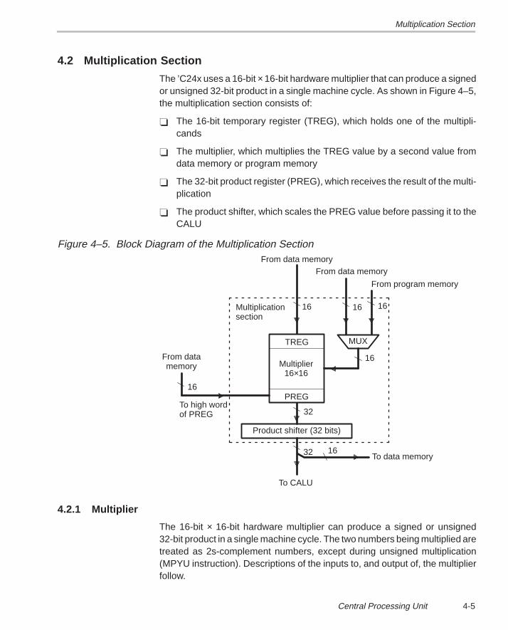
Multiplication Section
4-5Central Processing Unit
4.2 Multiplication Section
The ’C24x uses a 16-bit × 16-bit hardware multiplier that can produce a signedor unsigned 32-bit product in a single machine cycle. As shown in Figure 4–5,the multiplication section consists of:
The 16-bit temporary register (TREG), which holds one of the multipli-cands
The multiplier, which multiplies the TREG value by a second value fromdata memory or program memory
The 32-bit product register (PREG), which receives the result of the multi-plication
The product shifter, which scales the PREG value before passing it to theCALU
Figure 4–5. Block Diagram of the Multiplication Section
32
MUX
PREG
Multiplier16×16
16
TREG
Product shifter (32 bits)
Multiplicationsection
From data memory
16
From datamemory
16
From program memory
16
To CALU
32
From data memory
16
16To data memory
To high wordof PREG
4.2.1 Multiplier
The 16-bit × 16-bit hardware multiplier can produce a signed or unsigned32-bit product in a single machine cycle. The two numbers being multiplied aretreated as 2s-complement numbers, except during unsigned multiplication(MPYU instruction). Descriptions of the inputs to, and output of, the multiplierfollow.
Multiplication Section
4-6
Inputs . The multiplier accepts two 16-bit inputs:
One input is always from the 16-bit temporary register (TREG). The TREGis loaded before the multiplication with a data-value from the data read bus(DRDB).
The other input is one of the following:
A data-memory value from the data read bus (DRDB) A program memory value from the program read bus (PRDB)
Output . After the two 16-bit inputs are multiplied, the 32-bit result is stored inthe product register (PREG). The output of the PREG is connected to the 32-bitproduct-scaling shifter. Through this shifter, the product is transferred from thePREG to the CALU or to data memory (by the SPH and SPL instructions).
4.2.2 Product-Scaling Shifter
The product-scaling shifter (product shifter) facilitates scaling of the productregister (PREG) value. The shifter has a 32-bit input connected to the outputof the PREG and a 32-bit output connected to the input of the CALU.
Input . The shifter has a 32-bit input connected to the output of the PREG.
Output . After the shifter completes the shift, all 32 bits of the result can bepassed to the CALU, or 16 bits of the result can be stored to data memory.
Shift Modes . This shifter uses one of four product shift modes, summarizedin Table 4–1. As shown in the table, these modes are determined by the prod-uct shift mode (PM) bits of status register ST1. In the first shift mode (PM = 00),the shifter does not shift the product at all before giving it to the CALU or to datamemory. The next two modes cause left shifts (of one or four), which are usefulfor implementing fractional arithmetic or justifying products. The right-shiftmode shifts the product by six bits, enabling the execution of up to 128 consec-utive multiply-and-accumulate operations without causing the accumulator tooverflow. Note that the content of the PREG remains unchanged; the value iscopied to the product shifter and shifted there.
Note:
The right shift in the product shifter is always sign extended, regardless ofthe value of the sign-extension mode bit (SXM) of status register ST1.
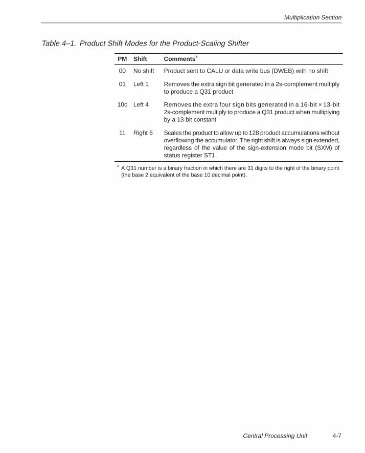
Multiplication Section
4-7Central Processing Unit
Table 4–1. Product Shift Modes for the Product-Scaling Shifter
ÁÁÁÁ
PMÁÁÁÁÁÁÁÁ
Shift ÁÁÁÁÁÁÁÁÁÁÁÁÁÁÁÁÁÁÁÁÁÁÁÁÁÁÁÁÁÁÁÁÁÁÁÁÁÁ
Comments †
ÁÁÁÁ
00ÁÁÁÁÁÁÁÁ
No shiftÁÁÁÁÁÁÁÁÁÁÁÁÁÁÁÁÁÁÁÁÁÁÁÁÁÁÁÁÁÁÁÁÁÁÁÁÁÁ
Product sent to CALU or data write bus (DWEB) with no shiftÁÁÁÁÁÁ
01ÁÁÁÁÁÁÁÁÁÁÁÁ
Left 1ÁÁÁÁÁÁÁÁÁÁÁÁÁÁÁÁÁÁÁÁÁÁÁÁÁÁÁÁÁÁÁÁÁÁÁÁÁÁÁÁÁÁÁÁÁÁÁÁÁÁÁÁÁÁÁÁÁ
Removes the extra sign bit generated in a 2s-complement multiplyto produce a Q31 product
ÁÁÁÁÁÁÁÁ
10cÁÁÁÁÁÁÁÁÁÁÁÁÁÁÁÁ
Left 4ÁÁÁÁÁÁÁÁÁÁÁÁÁÁÁÁÁÁÁÁÁÁÁÁÁÁÁÁÁÁÁÁÁÁÁÁÁÁÁÁÁÁÁÁÁÁÁÁÁÁÁÁÁÁÁÁÁÁÁÁÁÁÁÁÁÁÁÁÁÁÁÁÁÁÁÁ
Removes the extra four sign bits generated in a 16-bit × 13-bit2s-complement multiply to produce a Q31 product when multiplyingby a 13-bit constant
ÁÁÁÁÁÁÁÁ
11ÁÁÁÁÁÁÁÁÁÁÁÁÁÁÁÁ
Right 6ÁÁÁÁÁÁÁÁÁÁÁÁÁÁÁÁÁÁÁÁÁÁÁÁÁÁÁÁÁÁÁÁÁÁÁÁÁÁÁÁÁÁÁÁÁÁÁÁÁÁÁÁÁÁÁÁÁÁÁÁÁÁÁÁÁÁÁÁÁÁÁÁÁÁÁÁ
Scales the product to allow up to 128 product accumulations withoutoverflowing the accumulator. The right shift is always sign extended,regardless of the value of the sign-extension mode bit (SXM) ofstatus register ST1.
ÁÁÁÁÁÁÁÁÁÁÁÁÁÁÁÁÁÁÁÁÁÁÁÁÁÁÁÁÁÁÁÁÁÁÁÁÁÁÁÁÁÁÁÁÁÁÁÁÁÁÁÁÁÁÁÁÁÁÁÁÁÁÁÁÁÁÁÁÁ
† A Q31 number is a binary fraction in which there are 31 digits to the right of the binary point(the base 2 equivalent of the base 10 decimal point).
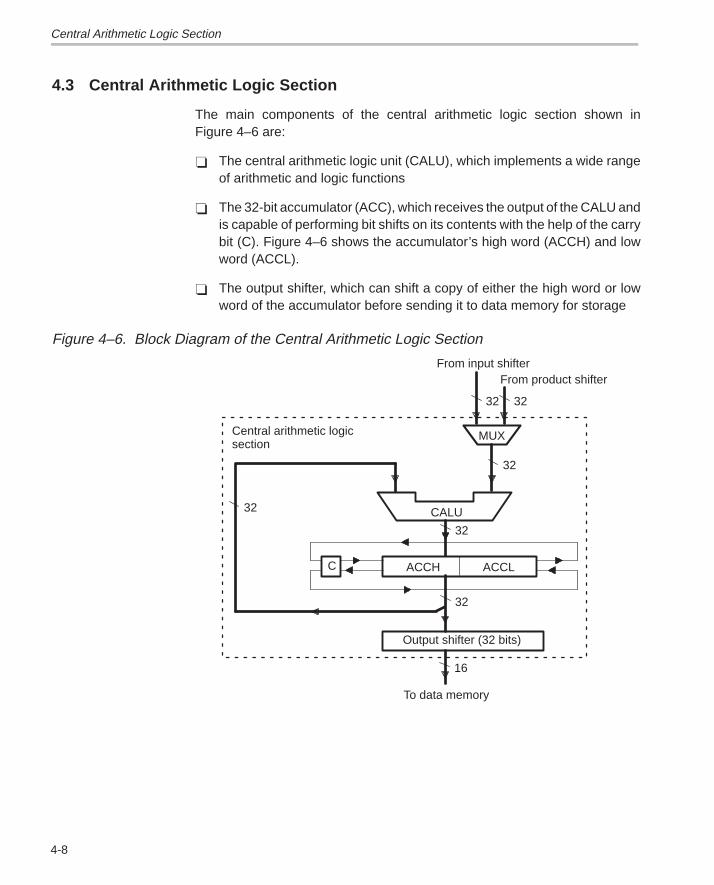
Central Arithmetic Logic Section
4-8
4.3 Central Arithmetic Logic Section
The main components of the central arithmetic logic section shown inFigure 4–6 are:
The central arithmetic logic unit (CALU), which implements a wide rangeof arithmetic and logic functions
The 32-bit accumulator (ACC), which receives the output of the CALU andis capable of performing bit shifts on its contents with the help of the carrybit (C). Figure 4–6 shows the accumulator’s high word (ACCH) and lowword (ACCL).
The output shifter, which can shift a copy of either the high word or lowword of the accumulator before sending it to data memory for storage
Figure 4–6. Block Diagram of the Central Arithmetic Logic Section
ACCH
32
32
Output shifter (32 bits)
32
C ACCL
CALU
MUXCentral arithmetic logicsection
32
From product shifterFrom input shifter
3232
To data memory
16
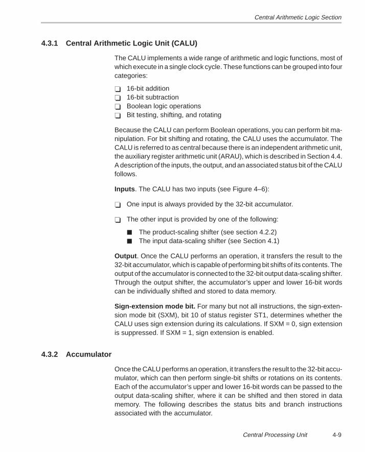
Central Arithmetic Logic Section
4-9Central Processing Unit
4.3.1 Central Arithmetic Logic Unit (CALU)
The CALU implements a wide range of arithmetic and logic functions, most ofwhich execute in a single clock cycle. These functions can be grouped into fourcategories:
16-bit addition 16-bit subtraction Boolean logic operations Bit testing, shifting, and rotating
Because the CALU can perform Boolean operations, you can perform bit ma-nipulation. For bit shifting and rotating, the CALU uses the accumulator. TheCALU is referred to as central because there is an independent arithmetic unit,the auxiliary register arithmetic unit (ARAU), which is described in Section 4.4.A description of the inputs, the output, and an associated status bit of the CALUfollows.
Inputs . The CALU has two inputs (see Figure 4–6):
One input is always provided by the 32-bit accumulator.
The other input is provided by one of the following:
The product-scaling shifter (see section 4.2.2) The input data-scaling shifter (see Section 4.1)
Output . Once the CALU performs an operation, it transfers the result to the32-bit accumulator, which is capable of performing bit shifts of its contents. Theoutput of the accumulator is connected to the 32-bit output data-scaling shifter.Through the output shifter, the accumulator’s upper and lower 16-bit wordscan be individually shifted and stored to data memory.
Sign-extension mode bit. For many but not all instructions, the sign-exten-sion mode bit (SXM), bit 10 of status register ST1, determines whether theCALU uses sign extension during its calculations. If SXM = 0, sign extensionis suppressed. If SXM = 1, sign extension is enabled.
4.3.2 Accumulator
Once the CALU performs an operation, it transfers the result to the 32-bit accu-mulator, which can then perform single-bit shifts or rotations on its contents.Each of the accumulator’s upper and lower 16-bit words can be passed to theoutput data-scaling shifter, where it can be shifted and then stored in datamemory. The following describes the status bits and branch instructionsassociated with the accumulator.
Central Arithmetic Logic Section
4-10
Status bits . Four status bits are associated with the accumulator:
Carry bit (C). C (bit 9 of status register ST1) is affected during:
Additions to and subtractions from the accumulator:
C = 0 When the result of a subtraction generates a borrow
When the result of an addition does not generate a carry(Exception: When the ADD instruction is used with a shiftof 16 and no carry is generated, the ADD instruction hasno effect on C.)
C = 1 When the result of an addition generates a carry
When the result of a subtraction does not generate a bor-row (Exception: When the SUB instruction is used with ashift of 16 and no borrow is generated, the SUB instructionhas no effect on C.)
Single-bit shifts and rotations of the accumulator value. During a leftshift or rotation, the MSB of the accumulator is passed to C; during aright shift or rotation, the LSB is passed to C.
Overflow mode bit (OVM). OVM (bit 11 of status register ST0) determineshow the accumulator reflects arithmetic overflows. When the processor isin overflow mode (OVM = 1) and an overflow occurs, the accumulator isfilled with one of two specific values:
If the overflow is in the positive direction, the accumulator is filled withits most positive value (7FFF FFFFh).
If the overflow is in the negative direction, the accumulator is filled withits most negative value (8000 0000h).
Overflow flag bit (OV). OV is bit 12 of status register ST0. When no accu-mulator overflow is detected, OV is latched at 0. When overflow (positiveor negative) occurs, OV is set to 1 and latched.
Test/control flag bit (TC). TC (bit 11 of status register ST1) is set to 0 or 1depending on the value of a tested bit. In the case of the NORM instruction,if the exclusive-OR of the two MSBs of the accumulator is true, TC is setto 1.
A number of branch instructions are implemented, based on the status of bitsC, OV, and TC, and on the value in the accumulator (as compared to 0). Formore information about these instructions, see Section 5.4, ConditionalBranches, Calls, and Returns, on page 5-10.
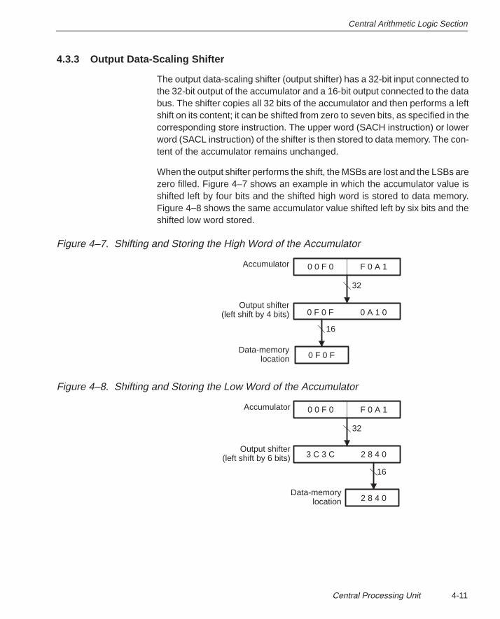
Central Arithmetic Logic Section
4-11Central Processing Unit
4.3.3 Output Data-Scaling Shifter
The output data-scaling shifter (output shifter) has a 32-bit input connected tothe 32-bit output of the accumulator and a 16-bit output connected to the databus. The shifter copies all 32 bits of the accumulator and then performs a leftshift on its content; it can be shifted from zero to seven bits, as specified in thecorresponding store instruction. The upper word (SACH instruction) or lowerword (SACL instruction) of the shifter is then stored to data memory. The con-tent of the accumulator remains unchanged.
When the output shifter performs the shift, the MSBs are lost and the LSBs arezero filled. Figure 4–7 shows an example in which the accumulator value isshifted left by four bits and the shifted high word is stored to data memory.Figure 4–8 shows the same accumulator value shifted left by six bits and theshifted low word stored.
Figure 4–7. Shifting and Storing the High Word of the Accumulator
Data-memorylocation
0 0 F 0 F 0 A 1
0 F 0 F 0 A 1 0
32
Output shifter(left shift by 4 bits)
Accumulator
16
0 F 0 F
Figure 4–8. Shifting and Storing the Low Word of the Accumulator
Data-memorylocation
0 0 F 0 F 0 A 1
3 C 3 C 2 8 4 0
32
Output shifter(left shift by 6 bits)
Accumulator
16
2 8 4 0
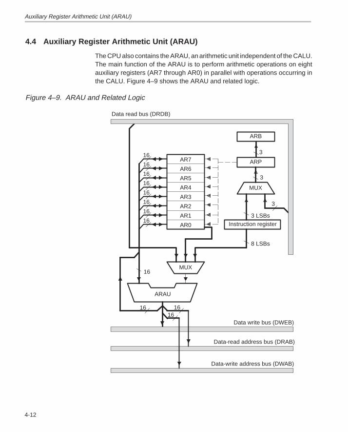
Auxiliary Register Arithmetic Unit (ARAU)
4-12
4.4 Auxiliary Register Arithmetic Unit (ARAU)
The CPU also contains the ARAU, an arithmetic unit independent of the CALU.The main function of the ARAU is to perform arithmetic operations on eightauxiliary registers (AR7 through AR0) in parallel with operations occurring inthe CALU. Figure 4–9 shows the ARAU and related logic.
Figure 4–9. ARAU and Related Logic
16
3
16
16
16
16
16
16
16
16
Data write bus (DWEB)
ARAU
ARB
3
8 LSBs
3 LSBsInstruction register
MUX
Data read bus (DRDB)
MUX
ARP
AR0
AR1
AR2
AR3
AR4
AR5
AR6
AR7
16
16
3
Data-read address bus (DRAB)
Data-write address bus (DWAB)
16
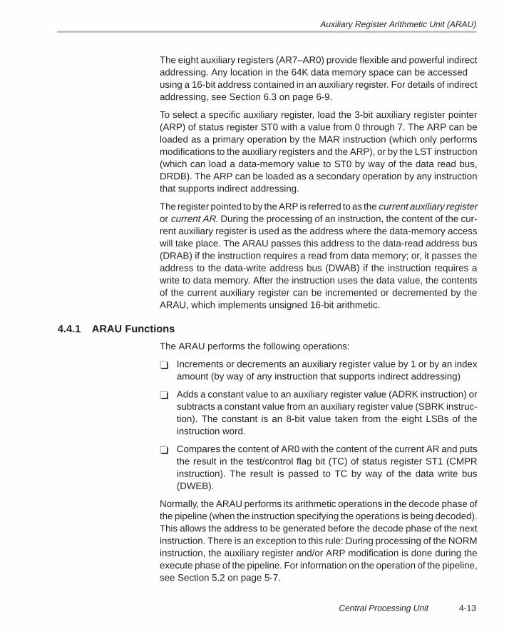
Auxiliary Register Arithmetic Unit (ARAU)
4-13Central Processing Unit
The eight auxiliary registers (AR7–AR0) provide flexible and powerful indirectaddressing. Any location in the 64K data memory space can be accessed using a 16-bit address contained in an auxiliary register. For details of indirectaddressing, see Section 6.3 on page 6-9.
To select a specific auxiliary register, load the 3-bit auxiliary register pointer(ARP) of status register ST0 with a value from 0 through 7. The ARP can beloaded as a primary operation by the MAR instruction (which only performsmodifications to the auxiliary registers and the ARP), or by the LST instruction(which can load a data-memory value to ST0 by way of the data read bus,DRDB). The ARP can be loaded as a secondary operation by any instructionthat supports indirect addressing.
The register pointed to by the ARP is referred to as the current auxiliary registeror current AR. During the processing of an instruction, the content of the cur-rent auxiliary register is used as the address where the data-memory accesswill take place. The ARAU passes this address to the data-read address bus(DRAB) if the instruction requires a read from data memory; or, it passes theaddress to the data-write address bus (DWAB) if the instruction requires awrite to data memory. After the instruction uses the data value, the contentsof the current auxiliary register can be incremented or decremented by theARAU, which implements unsigned 16-bit arithmetic.
4.4.1 ARAU Functions
The ARAU performs the following operations:
Increments or decrements an auxiliary register value by 1 or by an indexamount (by way of any instruction that supports indirect addressing)
Adds a constant value to an auxiliary register value (ADRK instruction) orsubtracts a constant value from an auxiliary register value (SBRK instruc-tion). The constant is an 8-bit value taken from the eight LSBs of theinstruction word.
Compares the content of AR0 with the content of the current AR and putsthe result in the test/control flag bit (TC) of status register ST1 (CMPRinstruction). The result is passed to TC by way of the data write bus(DWEB).
Normally, the ARAU performs its arithmetic operations in the decode phase ofthe pipeline (when the instruction specifying the operations is being decoded).This allows the address to be generated before the decode phase of the nextinstruction. There is an exception to this rule: During processing of the NORMinstruction, the auxiliary register and/or ARP modification is done during theexecute phase of the pipeline. For information on the operation of the pipeline,see Section 5.2 on page 5-7.
Auxiliary Register Arithmetic Unit (ARAU)
4-14
4.4.2 Auxiliary Register Functions
In addition to using the auxiliary registers to reference data-memory address-es, you can use them for other purposes. For example, you can:
Use the auxiliary registers to support conditional branches, calls, and re-turns by using the CMPR instruction. This instruction compares the con-tent of AR0 with the content of the current AR and puts the result in thetest/control flag bit (TC) of status register ST1.
Use the auxiliary registers for temporary storage by using the LAR instruc-tion to load values into the registers and the SAR instruction to store ARvalues to data memory
Use the auxiliary registers as software counters, incrementing or decre-menting them as necessary
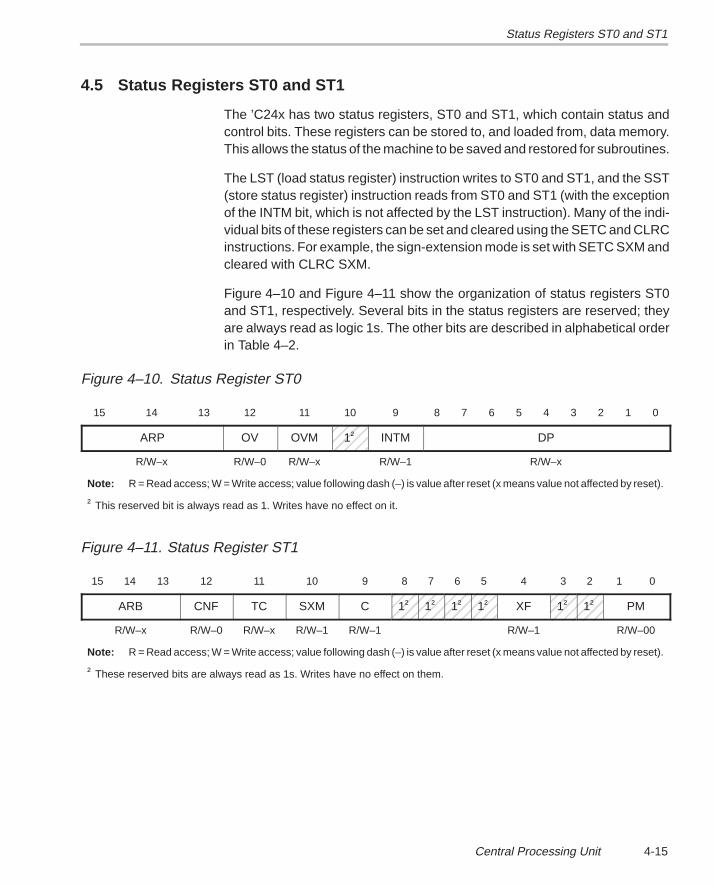
Status Registers ST0 and ST1
4-15Central Processing Unit
4.5 Status Registers ST0 and ST1
The ’C24x has two status registers, ST0 and ST1, which contain status andcontrol bits. These registers can be stored to, and loaded from, data memory.This allows the status of the machine to be saved and restored for subroutines.
The LST (load status register) instruction writes to ST0 and ST1, and the SST(store status register) instruction reads from ST0 and ST1 (with the exceptionof the INTM bit, which is not affected by the LST instruction). Many of the indi-vidual bits of these registers can be set and cleared using the SETC and CLRCinstructions. For example, the sign-extension mode is set with SETC SXM andcleared with CLRC SXM.
Figure 4–10 and Figure 4–11 show the organization of status registers ST0and ST1, respectively. Several bits in the status registers are reserved; theyare always read as logic 1s. The other bits are described in alphabetical orderin Table 4–2.
Figure 4–10. Status Register ST0
15 14 13 12 11 10 9 8 7 6 5 4 3 2 1 0
ARP OV OVMÉÉÉÉÉÉ
1† INTM DP
R/W–x R/W–0 R/W–x R/W–1 R/W–x
Note: R = Read access; W = Write access; value following dash (–) is value after reset (x means value not affected by reset).
† This reserved bit is always read as 1. Writes have no effect on it.
Figure 4–11. Status Register ST1
15 14 13 12 11 10 9 8 7 6 5 4 3 2 1 0
ARB CNF TC SXM C ÉÉÉÉ
1†ÉÉÉÉÉÉ
1† ÉÉÉÉ
1†ÉÉÉÉ
1† XF ÉÉÉÉ
1†ÉÉÉÉ
1† PM
R/W–x R/W–0 R/W–x R/W–1 R/W–1 R/W–1 R/W–00
Note: R = Read access; W = Write access; value following dash (–) is value after reset (x means value not affected by reset).
† These reserved bits are always read as 1s. Writes have no effect on them.
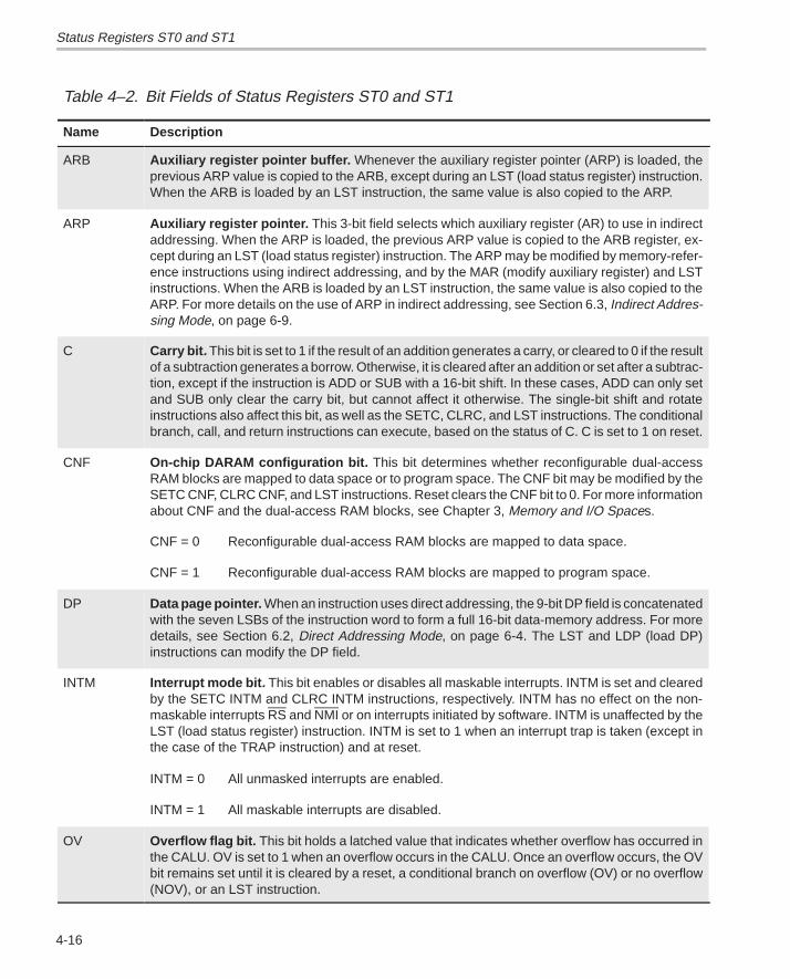
Status Registers ST0 and ST1
4-16
Table 4–2. Bit Fields of Status Registers ST0 and ST1
Name Description
ARB Auxiliary register pointer buffer. Whenever the auxiliary register pointer (ARP) is loaded, theprevious ARP value is copied to the ARB, except during an LST (load status register) instruction.When the ARB is loaded by an LST instruction, the same value is also copied to the ARP.
ARP Auxiliary register pointer. This 3-bit field selects which auxiliary register (AR) to use in indirectaddressing. When the ARP is loaded, the previous ARP value is copied to the ARB register, ex-cept during an LST (load status register) instruction. The ARP may be modified by memory-refer-ence instructions using indirect addressing, and by the MAR (modify auxiliary register) and LSTinstructions. When the ARB is loaded by an LST instruction, the same value is also copied to theARP. For more details on the use of ARP in indirect addressing, see Section 6.3, Indirect Addres-sing Mode, on page 6-9.
C Carry bit . This bit is set to 1 if the result of an addition generates a carry, or cleared to 0 if the resultof a subtraction generates a borrow. Otherwise, it is cleared after an addition or set after a subtrac-tion, except if the instruction is ADD or SUB with a 16-bit shift. In these cases, ADD can only setand SUB only clear the carry bit, but cannot affect it otherwise. The single-bit shift and rotateinstructions also affect this bit, as well as the SETC, CLRC, and LST instructions. The conditionalbranch, call, and return instructions can execute, based on the status of C. C is set to 1 on reset.
CNF On-chip DARAM configuration bit . This bit determines whether reconfigurable dual-accessRAM blocks are mapped to data space or to program space. The CNF bit may be modified by theSETC CNF, CLRC CNF, and LST instructions. Reset clears the CNF bit to 0. For more informationabout CNF and the dual-access RAM blocks, see Chapter 3, Memory and I/O Spaces.
CNF = 0 Reconfigurable dual-access RAM blocks are mapped to data space.
CNF = 1 Reconfigurable dual-access RAM blocks are mapped to program space.
DP Data page pointer. When an instruction uses direct addressing, the 9-bit DP field is concatenatedwith the seven LSBs of the instruction word to form a full 16-bit data-memory address. For moredetails, see Section 6.2, Direct Addressing Mode, on page 6-4. The LST and LDP (load DP)instructions can modify the DP field.
INTM Interrupt mode bit . This bit enables or disables all maskable interrupts. INTM is set and clearedby the SETC INTM and CLRC INTM instructions, respectively. INTM has no effect on the non-maskable interrupts RS and NMI or on interrupts initiated by software. INTM is unaffected by theLST (load status register) instruction. INTM is set to 1 when an interrupt trap is taken (except inthe case of the TRAP instruction) and at reset.
INTM = 0 All unmasked interrupts are enabled.
INTM = 1 All maskable interrupts are disabled.
OV Overflow flag bit. This bit holds a latched value that indicates whether overflow has occurred inthe CALU. OV is set to 1 when an overflow occurs in the CALU. Once an overflow occurs, the OVbit remains set until it is cleared by a reset, a conditional branch on overflow (OV) or no overflow(NOV), or an LST instruction.
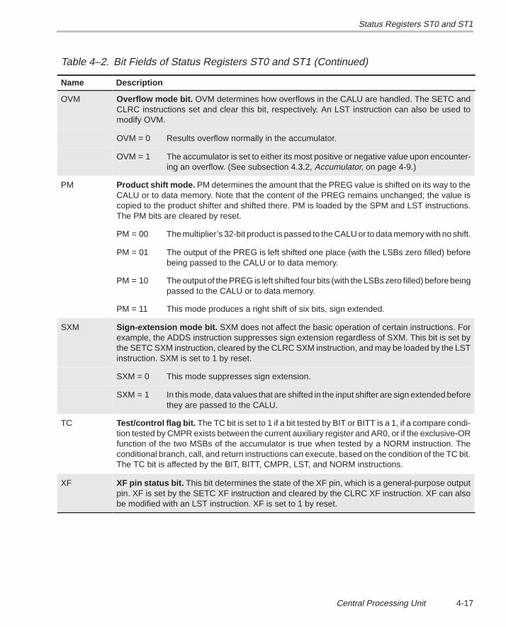
Status Registers ST0 and ST1
4-17Central Processing Unit
Table 4–2. Bit Fields of Status Registers ST0 and ST1 (Continued)
Name Description
OVM Overflow mode bit. OVM determines how overflows in the CALU are handled. The SETC andCLRC instructions set and clear this bit, respectively. An LST instruction can also be used tomodify OVM.
OVM = 0 Results overflow normally in the accumulator.
OVM = 1 The accumulator is set to either its most positive or negative value upon encounter-ing an overflow. (See subsection 4.3.2, Accumulator, on page 4-9.)
PM Product shift mode. PM determines the amount that the PREG value is shifted on its way to theCALU or to data memory. Note that the content of the PREG remains unchanged; the value iscopied to the product shifter and shifted there. PM is loaded by the SPM and LST instructions.The PM bits are cleared by reset.
PM = 00 The multiplier’s 32-bit product is passed to the CALU or to data memory with no shift.
PM = 01 The output of the PREG is left shifted one place (with the LSBs zero filled) beforebeing passed to the CALU or to data memory.
PM = 10 The output of the PREG is left shifted four bits (with the LSBs zero filled) before beingpassed to the CALU or to data memory.
PM = 11 This mode produces a right shift of six bits, sign extended.
SXM Sign-extension mode bit. SXM does not affect the basic operation of certain instructions. Forexample, the ADDS instruction suppresses sign extension regardless of SXM. This bit is set bythe SETC SXM instruction, cleared by the CLRC SXM instruction, and may be loaded by the LSTinstruction. SXM is set to 1 by reset.
SXM = 0 This mode suppresses sign extension.
SXM = 1 In this mode, data values that are shifted in the input shifter are sign extended beforethey are passed to the CALU.
TC Test/control flag bit. The TC bit is set to 1 if a bit tested by BIT or BITT is a 1, if a compare condi-tion tested by CMPR exists between the current auxiliary register and AR0, or if the exclusive-ORfunction of the two MSBs of the accumulator is true when tested by a NORM instruction. Theconditional branch, call, and return instructions can execute, based on the condition of the TC bit.The TC bit is affected by the BIT, BITT, CMPR, LST, and NORM instructions.
XF XF pin status bit . This bit determines the state of the XF pin, which is a general-purpose outputpin. XF is set by the SETC XF instruction and cleared by the CLRC XF instruction. XF can alsobe modified with an LST instruction. XF is set to 1 by reset.
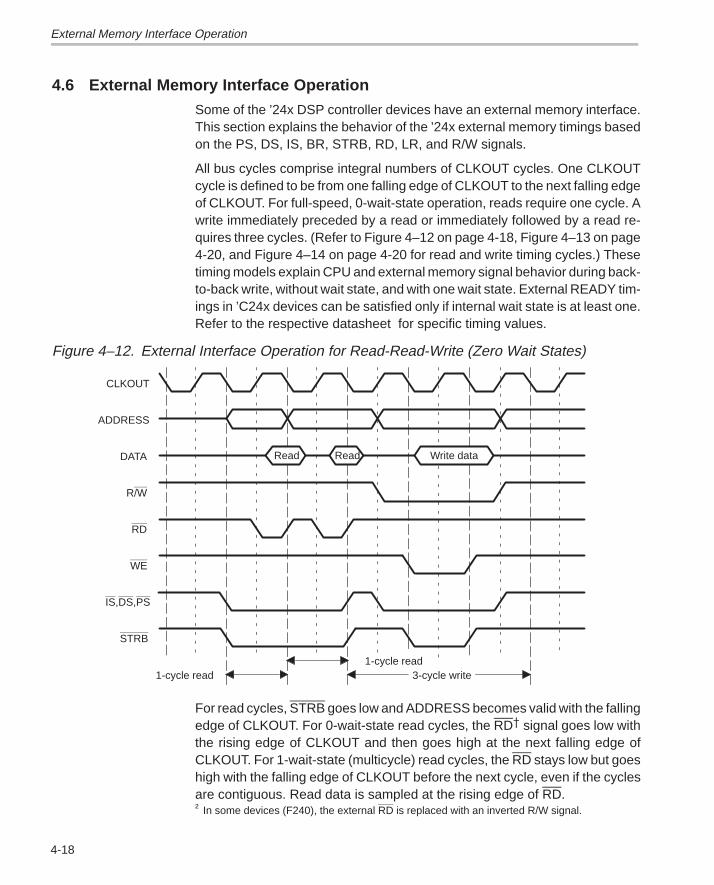
External Memory Interface Operation
4-18
4.6 External Memory Interface Operation
Some of the ’24x DSP controller devices have an external memory interface.This section explains the behavior of the ’24x external memory timings basedon the PS, DS, IS, BR, STRB, RD, LR, and R/W signals.
All bus cycles comprise integral numbers of CLKOUT cycles. One CLKOUTcycle is defined to be from one falling edge of CLKOUT to the next falling edgeof CLKOUT. For full-speed, 0-wait-state operation, reads require one cycle. Awrite immediately preceded by a read or immediately followed by a read re-quires three cycles. (Refer to Figure 4–12 on page 4-18, Figure 4–13 on page4-20, and Figure 4–14 on page 4-20 for read and write timing cycles.) Thesetiming models explain CPU and external memory signal behavior during back-to-back write, without wait state, and with one wait state. External READY tim-ings in ’C24x devices can be satisfied only if internal wait state is at least one.Refer to the respective datasheet for specific timing values.
Figure 4–12. External Interface Operation for Read-Read-Write (Zero Wait States)
1-cycle read1-cycle read
ReadRead
STRB
IS,DS,PS
WE
RD
R/W
DATA
ADDRESS
CLKOUT
3-cycle write
Write data
For read cycles, STRB goes low and ADDRESS becomes valid with the fallingedge of CLKOUT. For 0-wait-state read cycles, the RD signal goes low withthe rising edge of CLKOUT and then goes high at the next falling edge ofCLKOUT. For 1-wait-state (multicycle) read cycles, the RD stays low but goeshigh with the falling edge of CLKOUT before the next cycle, even if the cyclesare contiguous. Read data is sampled at the rising edge of RD.† In some devices (F240), the external RD is replaced with an inverted R/W signal.
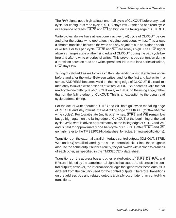
External Memory Interface Operation
4-19Central Processing Unit
The R/W signal goes high at least one-half cycle of CLKOUT before any readcycle; for contiguous read cycles, STRB stays low. At the end of a read cycleor sequence of reads, STRB and RD go high on the falling edge of CLKOUT.
Write cycles always have at least one inactive (pad) cycle of CLKOUT beforeand after the actual write operation, including contiguous writes. This allowsa smooth transition between the write and any adjacent bus operations or oth-er writes. For this pad cycle, STRB and WE are always high. The R/W signalalways changes state on the rising edge of CLKOUT during the pad cycle be-fore and after a write or series of writes. This prevents bus contention duringa transition between read and write operations. Note that for a series of writes,R/W stays low.
Timing of valid addresses for writes differs, depending on what activities occurbefore and after the write. Between writes, and for the first and last write in aseries, ADDRESS becomes valid on the rising edge of CLKOUT. If a read im-mediately follows a write or series of writes, ADDRESS becomes valid for thatread cycle one half-cycle of CLKOUT early — that is, on the rising edge, ratherthan on the falling edge, of CLKOUT. This is an exception to the usual readcycle address timing.
For the actual write operation, STRB and WE both go low on the falling edgeof CLKOUT and stay low until the next falling edge of CLKOUT (for 0-wait-statewrite cycles). For 1-wait-state (multicycle) writes, STRB and WE remain lowbut go high again on the falling edge of CLKOUT at the beginning of the padcycle. Write data is driven approximately at the falling edge of STRB and WEand is held for approximately one half-cycle of CLKOUT after STRB and WEgo high (refer to the TMS320C24x data sheet for actual timing specifications).
Transitions on the external parallel interface control outputs (CLKOUT, STRB,WE, and RD) are all initiated by the same internal clocks. Since these signalsalso use the same output buffer circuitry, they all switch within close tolerancesof each other, as specified in the TMS320C24x data sheet.
Transitions on the address bus and other related outputs (IS, PS, DS, R/W, andBR) are initiated by the same internal signals that cause transitions on the con-trol outputs; however, the internal device logic that generates these outputs isdifferent from the circuitry used for the control outputs. Therefore, transitionson the address bus and related outputs typically occur later than control-linetransitions.
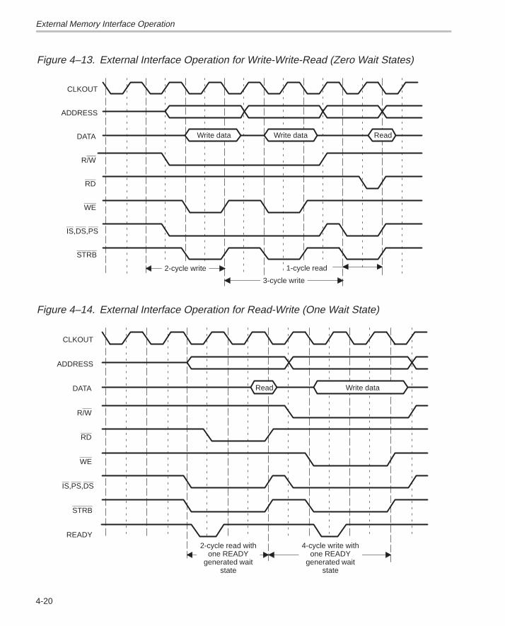
External Memory Interface Operation
4-20
Figure 4–13. External Interface Operation for Write-Write-Read (Zero Wait States)
STRB
IS,DS,PS
WE
RD
R/W
DATA
ADDRESS
CLKOUT
1-cycle read
Read
2-cycle write
3-cycle write
Write data Write data
Figure 4–14. External Interface Operation for Read-Write (One Wait State)
Read
2-cycle read withone READY
generated waitstate
4-cycle write withone READY
generated waitstate
STRB
IS,PS,DS
WE
RD
R/W
DATA
ADDRESS
CLKOUT
READY
Write data
5-1
Program Control
This chapter discusses the processes and features involved in controlling theflow of a program on the ’C24x.
Program control involves controlling the order in which one or more blocks ofinstructions are executed. Normally, the flow of a program is sequential; the’C24x executes instructions at consecutive program-memory addresses. Attimes, a program must branch to a nonsequential address and then executeinstructions sequentially at that new location. For this purpose, the ’C24x sup-ports branches, calls, returns, repeats, and interrupts.
Topic Page
5.1 Program-Address Generation 5-2. . . . . . . . . . . . . . . . . . . . . . . . . . . . . . . . . .
5.2 Pipeline Operation 5-7. . . . . . . . . . . . . . . . . . . . . . . . . . . . . . . . . . . . . . . . . . . .
5.3 Branches, Calls, and Returns 5-8. . . . . . . . . . . . . . . . . . . . . . . . . . . . . . . . . .
5.4 Conditional Branches, Calls, and Returns 5-10. . . . . . . . . . . . . . . . . . . . . .
5.5 Repeating a Single Instruction 5-14. . . . . . . . . . . . . . . . . . . . . . . . . . . . . . . .
5.6 Interrupts 5-15. . . . . . . . . . . . . . . . . . . . . . . . . . . . . . . . . . . . . . . . . . . . . . . . . . .
5.7 CPU Interrupt Registers 5-17. . . . . . . . . . . . . . . . . . . . . . . . . . . . . . . . . . . . . .
Chapter 5
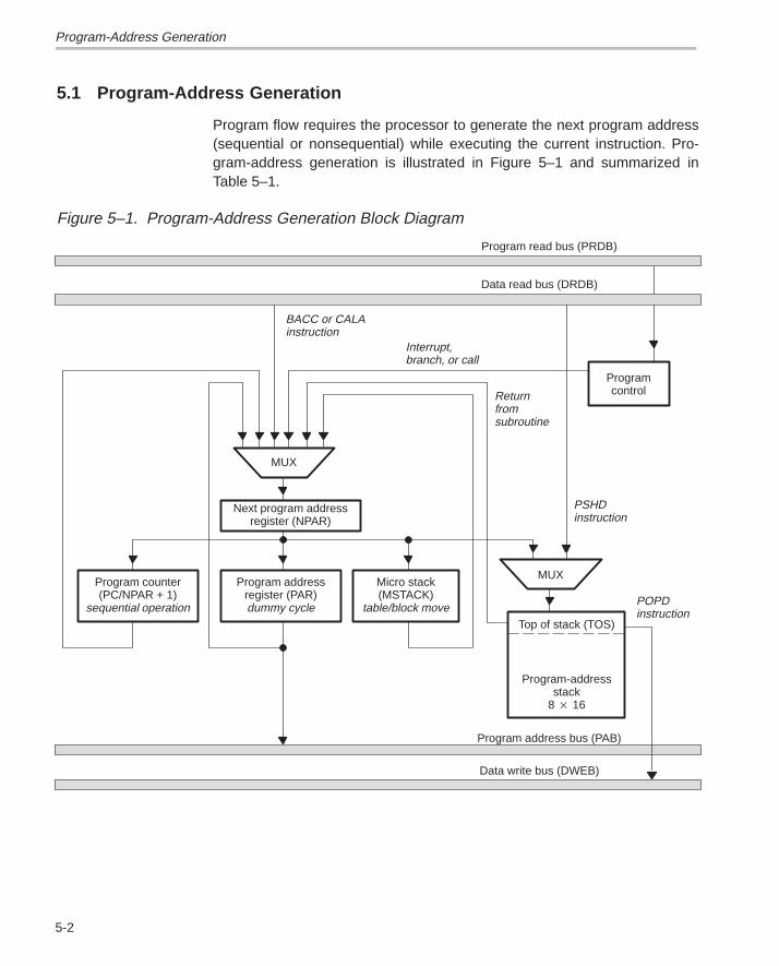
Program-Address Generation
5-2
5.1 Program-Address Generation
Program flow requires the processor to generate the next program address(sequential or nonsequential) while executing the current instruction. Pro-gram-address generation is illustrated in Figure 5–1 and summarized inTable 5–1.
Figure 5–1. Program-Address Generation Block Diagram
Interrupt,branch, or call
ÁÁÁÁÁÁÁÁÁÁÁÁÁÁÁÁÁÁÁÁÁÁÁÁÁÁÁÁÁÁÁÁÁÁÁÁ
ÁÁÁÁÁÁÁÁÁÁÁÁ
ÁÁÁÁÁÁÁÁÁÁÁÁÁÁÁÁÁÁÁÁ
ÁÁÁÁÁÁÁÁÁÁÁÁÁÁÁÁÁÁÁÁÁÁÁÁÁÁÁÁ
ÁÁÁÁÁÁÁÁÁÁÁÁÁÁÁÁÁÁÁÁÁÁÁÁ
ÁÁÁÁÁÁÁÁÁÁÁÁÁÁÁÁÁÁÁÁÁ
ÁÁÁÁÁÁÁÁÁÁÁÁ
MUX
Next program addressregister (NPAR)
Program counter(PC/NPAR + 1)
sequential operation
Program addressregister (PAR)dummy cycle
Micro stack(MSTACK)
table/block move
MUX
Program read bus (PRDB)
Data read bus (DRDB)
Top of stack (TOS)
Program-addressstack
8 16
Program address bus (PAB)
Data write bus (DWEB)
PSHDinstruction
Returnfromsubroutine
POPDinstruction
Programcontrol
BACC or CALAinstruction
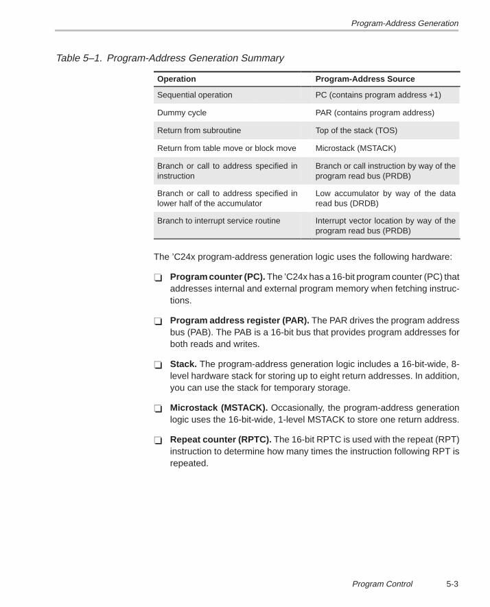
Program-Address Generation
5-3Program Control
Table 5–1. Program-Address Generation Summary
ÁÁÁÁÁÁÁÁÁÁÁÁÁÁÁÁÁÁÁÁÁÁ
Operation ÁÁÁÁÁÁÁÁÁÁÁÁÁÁÁÁÁÁÁÁÁÁÁÁÁÁÁÁ
Program-Address Source
Sequential operation PC (contains program address +1)ÁÁÁÁÁÁÁÁÁÁÁÁÁÁÁÁÁÁÁÁÁÁÁÁÁÁÁÁÁÁÁÁÁ
Dummy cycleÁÁÁÁÁÁ
ÁÁÁÁÁÁÁÁÁÁÁÁÁÁÁÁÁÁÁÁÁÁÁÁÁÁÁÁÁÁÁÁÁÁÁÁ
PAR (contains program address)
Return from subroutine Top of the stack (TOS)
ÁÁÁÁÁÁÁÁÁÁÁÁÁÁÁÁÁÁÁÁÁÁ
Return from table move or block moveÁÁÁÁÁÁÁÁÁÁÁÁÁÁÁÁÁÁÁÁÁÁÁÁÁÁÁÁ
Microstack (MSTACK)
Branch or call to address specified ininstruction
Branch or call instruction by way of theprogram read bus (PRDB)
ÁÁÁÁÁÁÁÁÁÁÁÁÁÁÁÁÁÁÁÁÁÁÁÁÁÁÁÁÁÁÁÁÁ
Branch or call to address specified inlower half of the accumulator
ÁÁÁÁÁÁ
ÁÁÁÁÁÁÁÁÁÁÁÁÁÁÁÁÁÁÁÁÁÁÁÁÁÁÁÁÁÁÁÁÁÁÁÁ
Low accumulator by way of the dataread bus (DRDB)
Branch to interrupt service routine Interrupt vector location by way of theprogram read bus (PRDB)
The ’C24x program-address generation logic uses the following hardware:
Program counter (PC). The ’C24x has a 16-bit program counter (PC) thataddresses internal and external program memory when fetching instruc-tions.
Program address register (PAR). The PAR drives the program addressbus (PAB). The PAB is a 16-bit bus that provides program addresses forboth reads and writes.
Stack. The program-address generation logic includes a 16-bit-wide, 8-level hardware stack for storing up to eight return addresses. In addition,you can use the stack for temporary storage.
Microstack (MSTACK). Occasionally, the program-address generationlogic uses the 16-bit-wide, 1-level MSTACK to store one return address.
Repeat counter (RPTC). The 16-bit RPTC is used with the repeat (RPT)instruction to determine how many times the instruction following RPT isrepeated.
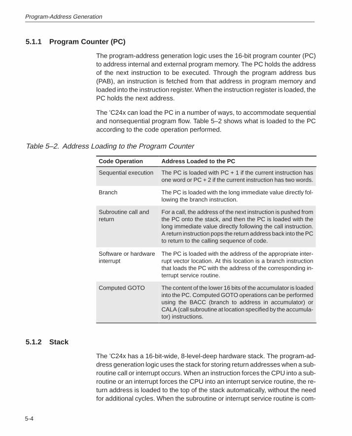
Program-Address Generation
5-4
5.1.1 Program Counter (PC)
The program-address generation logic uses the 16-bit program counter (PC)to address internal and external program memory. The PC holds the addressof the next instruction to be executed. Through the program address bus(PAB), an instruction is fetched from that address in program memory andloaded into the instruction register. When the instruction register is loaded, thePC holds the next address.
The ’C24x can load the PC in a number of ways, to accommodate sequentialand nonsequential program flow. Table 5–2 shows what is loaded to the PCaccording to the code operation performed.
Table 5–2. Address Loading to the Program CounterÁÁÁÁÁÁÁÁÁÁÁÁÁÁÁÁCode Operation
ÁÁÁÁÁÁÁÁÁÁÁÁÁÁÁÁÁÁÁÁÁÁÁÁÁÁÁÁÁÁÁÁAddress Loaded to the PC
Sequential execution The PC is loaded with PC + 1 if the current instruction hasone word or PC + 2 if the current instruction has two words.
ÁÁÁÁÁÁÁÁÁÁÁÁÁÁÁÁÁÁÁÁÁÁÁÁ
BranchÁÁÁÁÁÁÁÁÁÁÁÁÁÁÁÁÁÁÁÁÁÁÁÁÁÁÁÁÁÁÁÁÁÁÁÁÁÁÁÁÁÁÁÁÁÁÁÁ
The PC is loaded with the long immediate value directly fol-lowing the branch instruction.
Subroutine call andreturn
For a call, the address of the next instruction is pushed fromthe PC onto the stack, and then the PC is loaded with thelong immediate value directly following the call instruction.A return instruction pops the return address back into the PCto return to the calling sequence of code.
ÁÁÁÁÁÁÁÁÁÁÁÁÁÁÁÁÁÁÁÁÁÁÁÁÁÁÁÁÁÁÁÁÁÁÁÁÁÁÁÁ
Software or hardwareinterrupt
ÁÁÁÁÁÁÁÁÁÁÁÁÁÁÁÁÁÁÁÁÁÁÁÁÁÁÁÁÁÁÁÁÁÁÁÁÁÁÁÁÁÁÁÁÁÁÁÁÁÁÁÁÁÁÁÁÁÁÁÁÁÁÁÁÁÁÁÁÁÁÁÁÁÁÁÁÁÁÁÁ
The PC is loaded with the address of the appropriate inter-rupt vector location. At this location is a branch instructionthat loads the PC with the address of the corresponding in-terrupt service routine.
Computed GOTO The content of the lower 16 bits of the accumulator is loadedinto the PC. Computed GOTO operations can be performedusing the BACC (branch to address in accumulator) orCALA (call subroutine at location specified by the accumula-tor) instructions.
5.1.2 Stack
The ’C24x has a 16-bit-wide, 8-level-deep hardware stack. The program-ad-dress generation logic uses the stack for storing return addresses when a sub-routine call or interrupt occurs. When an instruction forces the CPU into a sub-routine or an interrupt forces the CPU into an interrupt service routine, the re-turn address is loaded to the top of the stack automatically, without the needfor additional cycles. When the subroutine or interrupt service routine is com-
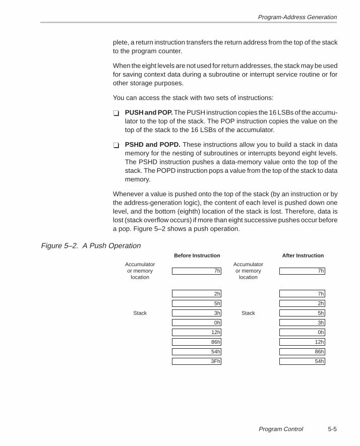
Program-Address Generation
5-5Program Control
plete, a return instruction transfers the return address from the top of the stackto the program counter.
When the eight levels are not used for return addresses, the stack may be usedfor saving context data during a subroutine or interrupt service routine or forother storage purposes.
You can access the stack with two sets of instructions:
PUSH and POP. The PUSH instruction copies the 16 LSBs of the accumu-lator to the top of the stack. The POP instruction copies the value on thetop of the stack to the 16 LSBs of the accumulator.
PSHD and POPD. These instructions allow you to build a stack in datamemory for the nesting of subroutines or interrupts beyond eight levels.The PSHD instruction pushes a data-memory value onto the top of thestack. The POPD instruction pops a value from the top of the stack to datamemory.
Whenever a value is pushed onto the top of the stack (by an instruction or bythe address-generation logic), the content of each level is pushed down onelevel, and the bottom (eighth) location of the stack is lost. Therefore, data islost (stack overflow occurs) if more than eight successive pushes occur beforea pop. Figure 5–2 shows a push operation.
Figure 5–2. A Push OperationBefore Instruction After Instruction
Accumulator Accumulatoror memory 7h or memory 7h
location location
2h 7h
5h 2h
Stack 3h Stack 5h
0h 3h
12h 0h
86h 12h
54h 86h
3Fh 54h
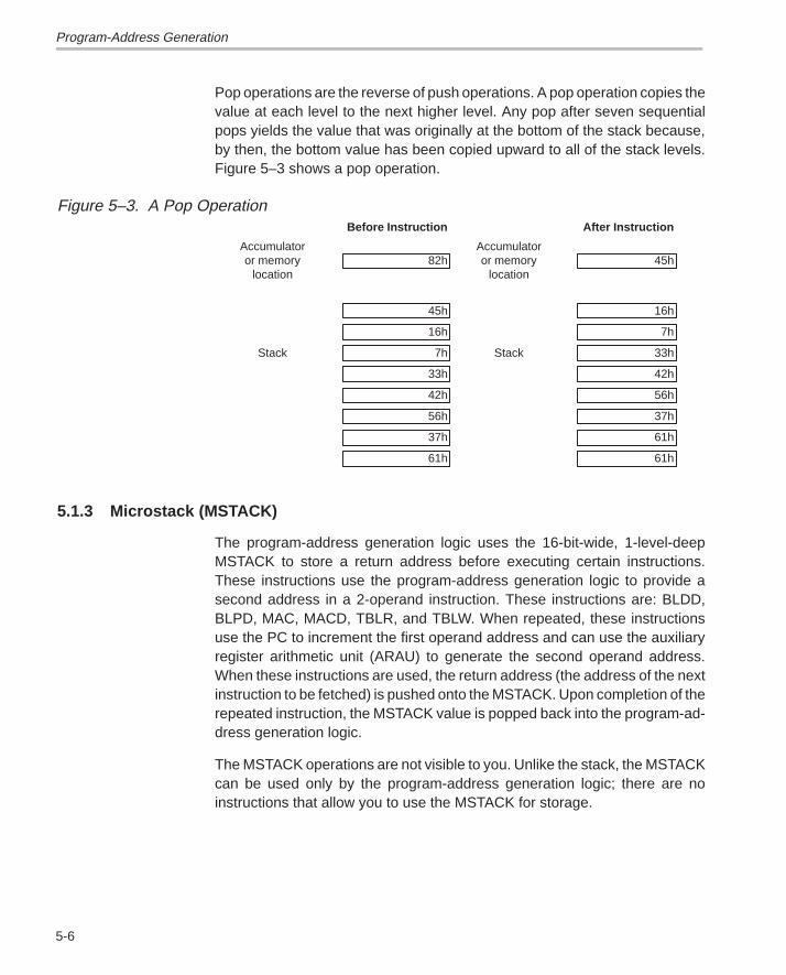
Program-Address Generation
5-6
Pop operations are the reverse of push operations. A pop operation copies thevalue at each level to the next higher level. Any pop after seven sequentialpops yields the value that was originally at the bottom of the stack because,by then, the bottom value has been copied upward to all of the stack levels.Figure 5–3 shows a pop operation.
Figure 5–3. A Pop OperationBefore Instruction After Instruction
Accumulator Accumulatoror memory 82h or memory 45h
location location
45h 16h
16h 7h
Stack 7h Stack 33h
33h 42h
42h 56h
56h 37h
37h 61h
61h 61h
5.1.3 Microstack (MSTACK)
The program-address generation logic uses the 16-bit-wide, 1-level-deepMSTACK to store a return address before executing certain instructions.These instructions use the program-address generation logic to provide asecond address in a 2-operand instruction. These instructions are: BLDD,BLPD, MAC, MACD, TBLR, and TBLW. When repeated, these instructionsuse the PC to increment the first operand address and can use the auxiliaryregister arithmetic unit (ARAU) to generate the second operand address.When these instructions are used, the return address (the address of the nextinstruction to be fetched) is pushed onto the MSTACK. Upon completion of therepeated instruction, the MSTACK value is popped back into the program-ad-dress generation logic.
The MSTACK operations are not visible to you. Unlike the stack, the MSTACKcan be used only by the program-address generation logic; there are noinstructions that allow you to use the MSTACK for storage.
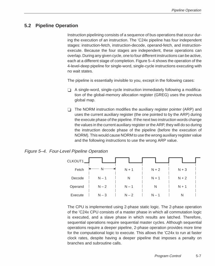
Pipeline Operation
5-7Program Control
5.2 Pipeline Operation
Instruction pipelining consists of a sequence of bus operations that occur dur-ing the execution of an instruction. The ’C24x pipeline has four independentstages: instruction-fetch, instruction-decode, operand-fetch, and instruction-execute. Because the four stages are independent, these operations canoverlap. During any given cycle, one to four different instructions can be active,each at a different stage of completion. Figure 5–4 shows the operation of the4-level-deep pipeline for single-word, single-cycle instructions executing withno wait states.
The pipeline is essentially invisible to you, except in the following cases:
A single-word, single-cycle instruction immediately following a modifica-tion of the global-memory allocation register (GREG) uses the previousglobal map.
The NORM instruction modifies the auxiliary register pointer (ARP) anduses the current auxiliary register (the one pointed to by the ARP) duringthe execute phase of the pipeline. If the next two instruction words changethe values in the current auxiliary register or the ARP, they will do so duringthe instruction decode phase of the pipeline (before the execution ofNORM). This would cause NORM to use the wrong auxiliary register valueand the following instructions to use the wrong ARP value.
Figure 5–4. Four-Level Pipeline Operation
N – 2N – 3
N – 2
N – 1
N – 1
N
N N + 1
N + 1 N + 2NN – 1
N + 3N + 2N + 1N
Execute
Operand
Decode
Fetch
CLKOUT1
The CPU is implemented using 2-phase static logic. The 2-phase operationof the ’C24x CPU consists of a master phase in which all commutation logicis executed, and a slave phase in which results are latched. Therefore,sequential operations require sequential master cycles. Although sequentialoperations require a deeper pipeline, 2-phase operation provides more timefor the computational logic to execute. This allows the ’C24x to run at fasterclock rates, despite having a deeper pipeline that imposes a penalty onbranches and subroutine calls.
Branches, Calls, and Returns
5-8
5.3 Branches, Calls, and Returns
Branches, calls, and returns break the sequential flow of instructions by trans-ferring control to another location in program memory. A branch only transferscontrol to the new location. A call also saves the return address (the addressof the instruction following the call) to the top of the hardware stack. Everycalled subroutine or interrupt service routine is concluded with a return instruc-tion, which pops the return address off the stack and back into the programcounter (PC).
The ’C24x has two types of branches, calls, and returns:
Unconditional. An unconditional branch, call, or return is alwaysexecuted. The unconditional branch, call, and return instructions are de-scribed in sections 5.3.1, 5.3.2, and 5.3.3, respectively.
Conditional. A conditional branch, call, or return is executed only if certainspecified conditions are met. The conditional branch, call, and returninstructions are described in detail in Section 5.4, Conditional Branches,Calls, and Returns, on page 5-10.
5.3.1 Unconditional Branches
When an unconditional branch is encountered, it is always executed. Duringthe execution, the PC is loaded with the specified program-memory addressand program execution begins at that address. The address loaded into thePC may come from either the second word of the branch instruction or the low-er sixteen bits of the accumulator.
By the time the branch instruction reaches the execute phase of the pipeline,the next two instruction words have already been fetched. These two instruc-tion words are flushed from the pipeline so that they are not executed, and thenexecution continues at the branched-to address. The unconditional branchinstructions are B (branch) and BACC (branch to location specified by accu-mulator).
5.3.2 Unconditional Calls
When an unconditional call is encountered, it is always executed. When thecall is executed, the PC is loaded with the specified program-memory addressand program execution begins at that address. The address loaded into thePC may come from either the second word of the call instruction or the lower16 bits of the accumulator. Before the PC is loaded, the return address is savedin the stack. After the subroutine or function is executed, a return instructionloads the PC with the return address from the stack, and execution resumesat the instruction following the call.
Branches, Calls, and Returns
5-9Program Control
By the time the unconditional call instruction reaches the execute phase of thepipeline, the next two instruction words have already been fetched. These twoinstruction words are flushed from the pipeline with the following results:
They are not executed.
The return address is stored to the stack.
Execution continues at the beginning of the called function.
The unconditional call instructions are CALL and CALA (call subroutine atlocation specified by accumulator).
5.3.3 Unconditional Returns
When an unconditional return (RET) instruction is encountered, it is alwaysexecuted. When the return is executed, the PC is loaded with the value at thetop of the stack, and execution resumes at that address.
By the time the unconditional return instruction reaches the execute phase ofthe pipeline, the next two instruction words have already been fetched. Thetwo instruction words are flushed from the pipeline with the following results:
They are not executed.
The return address is taken from the stack.
Execution continues in the calling function.
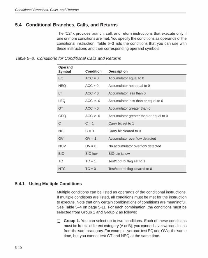
Conditional Branches, Calls, and Returns
5-10
5.4 Conditional Branches, Calls, and Returns
The ’C24x provides branch, call, and return instructions that execute only ifone or more conditions are met. You specify the conditions as operands of theconditional instruction. Table 5–3 lists the conditions that you can use withthese instructions and their corresponding operand symbols.
Table 5–3. Conditions for Conditional Calls and Returns
ÁÁÁÁÁÁÁÁÁÁÁÁ
OperandSymbol
ÁÁÁÁÁÁÁÁÁÁCondition
ÁÁÁÁÁÁÁÁÁÁÁÁÁÁÁÁÁÁÁÁÁÁÁÁÁÁÁÁDescription
EQ ACC = 0 Accumulator equal to 0
ÁÁÁÁÁÁÁÁÁÁÁÁ
NEQ ÁÁÁÁÁÁÁÁÁÁ
ACC ≠ 0 ÁÁÁÁÁÁÁÁÁÁÁÁÁÁÁÁÁÁÁÁÁÁÁÁÁÁÁÁ
Accumulator not equal to 0
LT ACC < 0 Accumulator less than 0ÁÁÁÁÁÁÁÁÁÁÁÁ
LEQÁÁÁÁÁÁÁÁÁÁ
ACC 0ÁÁÁÁÁÁÁÁÁÁÁÁÁÁÁÁÁÁÁÁÁÁÁÁÁÁÁÁ
Accumulator less than or equal to 0
GT ACC > 0 Accumulator greater than 0
ÁÁÁÁÁÁÁÁÁÁÁÁ
GEQ ÁÁÁÁÁÁÁÁÁÁ
ACC 0 ÁÁÁÁÁÁÁÁÁÁÁÁÁÁÁÁÁÁÁÁÁÁÁÁÁÁÁÁ
Accumulator greater than or equal to 0
C C = 1 Carry bit set to 1ÁÁÁÁÁÁÁÁÁÁÁÁNC
ÁÁÁÁÁÁÁÁÁÁC = 0
ÁÁÁÁÁÁÁÁÁÁÁÁÁÁÁÁÁÁÁÁÁÁÁÁÁÁÁÁCarry bit cleared to 0
OV OV = 1 Accumulator overflow detected
ÁÁÁÁÁÁÁÁÁÁÁÁ
NOV ÁÁÁÁÁÁÁÁÁÁ
OV = 0 ÁÁÁÁÁÁÁÁÁÁÁÁÁÁÁÁÁÁÁÁÁÁÁÁÁÁÁÁ
No accumulator overflow detected
BIO BIO low BIO pin is lowÁÁÁÁÁÁÁÁÁÁÁÁÁÁÁÁÁÁ
TCÁÁÁÁÁÁÁÁÁÁÁÁÁÁÁ
TC = 1ÁÁÁÁÁÁÁÁÁÁÁÁÁÁÁÁÁÁÁÁÁÁÁÁÁÁÁÁÁÁÁÁÁÁÁÁÁÁÁÁÁÁ
Test/control flag set to 1
NTC TC = 0 Test/control flag cleared to 0
5.4.1 Using Multiple Conditions
Multiple conditions can be listed as operands of the conditional instructions.If multiple conditions are listed, all conditions must be met for the instructionto execute. Note that only certain combinations of conditions are meaningful.See Table 5–4 on page 5-11. For each combination, the conditions must beselected from Group 1 and Group 2 as follows:
Group 1. You can select up to two conditions. Each of these conditionsmust be from a different category (A or B); you cannot have two conditionsfrom the same category. For example, you can test EQ and OV at the sametime, but you cannot test GT and NEQ at the same time.
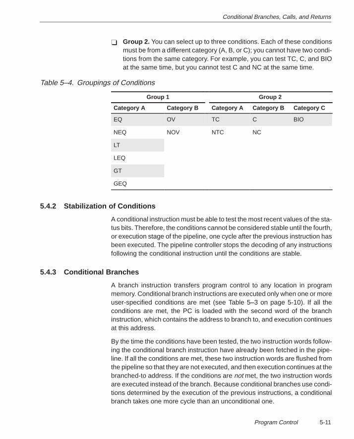
Conditional Branches, Calls, and Returns
5-11Program Control
Group 2. You can select up to three conditions. Each of these conditionsmust be from a different category (A, B, or C); you cannot have two condi-tions from the same category. For example, you can test TC, C, and BIOat the same time, but you cannot test C and NC at the same time.
Table 5–4. Groupings of Conditions
Group 1 Group 2
Category A Category B Category A Category B Category C
EQ OV TC C BIO
NEQ NOV NTC NC
LT
LEQ
GT
GEQ
5.4.2 Stabilization of Conditions
A conditional instruction must be able to test the most recent values of the sta-tus bits. Therefore, the conditions cannot be considered stable until the fourth,or execution stage of the pipeline, one cycle after the previous instruction hasbeen executed. The pipeline controller stops the decoding of any instructionsfollowing the conditional instruction until the conditions are stable.
5.4.3 Conditional Branches
A branch instruction transfers program control to any location in programmemory. Conditional branch instructions are executed only when one or moreuser-specified conditions are met (see Table 5–3 on page 5-10). If all theconditions are met, the PC is loaded with the second word of the branchinstruction, which contains the address to branch to, and execution continuesat this address.
By the time the conditions have been tested, the two instruction words follow-ing the conditional branch instruction have already been fetched in the pipe-line. If all the conditions are met, these two instruction words are flushed fromthe pipeline so that they are not executed, and then execution continues at thebranched-to address. If the conditions are not met, the two instruction wordsare executed instead of the branch. Because conditional branches use condi-tions determined by the execution of the previous instructions, a conditionalbranch takes one more cycle than an unconditional one.
Conditional Branches, Calls, and Returns
5-12
The conditional branch instructions are BCND (branch conditionally) andBANZ (branch if currently selected auxiliary register is not equal to 0). TheBANZ instruction is useful for implementing loops.
5.4.4 Conditional Calls
The conditional call (CC) instruction is executed only when the specified condi-tion or conditions are met (see Table 5–3 on page 5-10). This allows your pro-gram to choose among multiple subroutines based on the data being pro-cessed. If all the conditions are met, the PC is loaded with the second wordof the call instruction, which contains the starting address of the subroutine.Before branching to the subroutine, the processor stores the address of theinstruction following the call instruction (the return address) to the stack. Thefunction must end with a return instruction, which takes the return address offthe stack and forces the processor to resume execution of the calling program.
By the time the conditions of the conditional call instruction have been tested,the two instruction words following the call instruction have already beenfetched in the pipeline. If all the conditions are met, these two instruction wordsare flushed from the pipeline so that they are not executed, and then executioncontinues at the beginning of the called function. If the conditions are not met,the two instructions are executed instead of the call. Because there is a waitcycle for conditions to become stable, the conditional call takes one more cyclethan the unconditional one.
5.4.5 Conditional Returns
Returns are used in conjunction with calls and interrupts. A call or interruptstores a return address to the stack and then transfers program control to anew location in program memory. The called subroutine or the interrupt serviceroutine concludes with a return instruction, which pops the return address offthe top of the stack and into the program counter (PC).
The conditional return instruction (RETC) is executed only when one or moreconditions are met (see Table 5–3 on page 5-10). By using the RETC instruc-tion, you can give a subroutine or interrupt service routine more than one pos-sible return path. The path chosen then depends on the data being processed.In addition, you can use a conditional return to avoid conditionally branchingto/around the return instruction at the end of the subroutine or interrupt serviceroutine.
Conditional Branches, Calls, and Returns
5-13Program Control
If all the conditions are met for execution of the RETC instruction, the proces-sor loads the return address from the stack to the PC and resumes executionof the calling or interrupted program.
RETC, like RET, is a single-word instruction. However, because of the poten-tial PC discontinuity, it operates with the same effective execution time as theconditional branch (BCND) and the conditional call (CC). By the time the condi-tions of the conditional return instruction have been tested, the two instructionwords following the return instruction have already been fetched in the pipe-line. If all the conditions are met, these two instruction words are flushed fromthe pipeline so that they are not executed, and then execution of the callingprogram continues. If the conditions are not met, the two instructions areexecuted instead of the return. Because there is a wait cycle for conditions tobecome stable, the conditional return takes one more cycle than the uncondi-tional one.
Repeating a Single Instruction
5-14
5.5 Repeating a Single Instruction
The ’C24x repeat instruction (RPT) allows the execution of a single instructionN + 1 times, where N is specified as an operand of the RPT instruction. WhenRPT is executed, the repeat counter (RPTC) is loaded with N. RPTC is thendecremented every time the repeated instruction is executed, until RPTCequals 0. RPTC can be used as a 16-bit counter when the count value is readfrom a data-memory location; if the count value is specified as a constant oper-and, it is in an 8-bit counter.
The repeat feature is useful with instructions such as NORM (normalize con-tents of accumulator), MACD (multiply and accumulate with data move), andSUBC (conditional subtract). When instructions are repeated, the address anddata buses for program memory are free to fetch a second operand in parallelwith the address and data buses for data memory. This allows instructionssuch as MACD and BLPD to effectively execute in a single cycle whenrepeated.
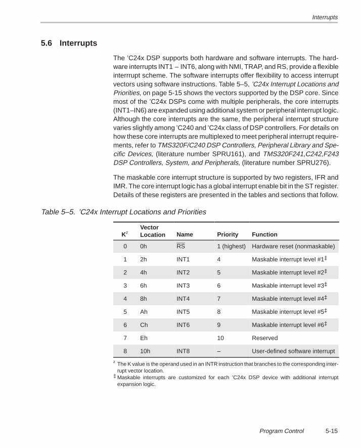
Interrupts
5-15Program Control
5.6 Interrupts
The ’C24x DSP supports both hardware and software interrupts. The hard-ware interrupts INT1 – INT6, along with NMI, TRAP, and RS, provide a flexibleinterrrupt scheme. The software interrupts offer flexibility to access interruptvectors using software instructions. Table 5–5, ’C24x Interrupt Locations andPriorities, on page 5-15 shows the vectors supported by the DSP core. Sincemost of the ’C24x DSPs come with multiple peripherals, the core interrupts(INT1–IN6) are expanded using additional system or peripheral interrupt logic.Although the core interrupts are the same, the peripheral interrupt structurevaries slightly among ’C240 and ’C24x class of DSP controllers. For details onhow these core interrupts are multiplexed to meet peripheral interrupt require-ments, refer to TMS320F/C240 DSP Controllers, Peripheral Library and Spe-cific Devices, (literature number SPRU161), and TMS320F241,C242,F243DSP Controllers, System, and Peripherals, (literature number SPRU276).
The maskable core interrupt structure is supported by two registers, IFR andIMR. The core interrupt logic has a global interrupt enable bit in the ST register.Details of these registers are presented in the tables and sections that follow.
Table 5–5. ’C24x Interrupt Locations and Priorities ÁÁÁÁÁÁÁÁÁ
K†
ÁÁÁÁÁÁÁÁÁÁÁÁÁÁÁ
VectorLocation
ÁÁÁÁÁÁÁÁÁÁÁÁÁÁÁ
Name
ÁÁÁÁÁÁÁÁÁÁÁÁPriority
ÁÁÁÁÁÁÁÁÁÁÁÁÁÁÁÁÁÁÁÁÁÁÁÁÁÁÁÁÁÁ
Function
0 0h RS 1 (highest) Hardware reset (nonmaskable)
1 2h INT1 4 Maskable interrupt level #1
2 4h INT2 5 Maskable interrupt level #2
3 6h INT3 6 Maskable interrupt level #3
4 8h INT4 7 Maskable interrupt level #4
5 Ah INT5 8 Maskable interrupt level #5
6 Ch INT6 9 Maskable interrupt level #6
7 Eh 10 Reserved
8 10h INT8 – User-defined software interrupt
† The K value is the operand used in an INTR instruction that branches to the corresponding inter-rupt vector location.
‡ Maskable interrupts are customized for each ’C24x DSP device with additional interruptexpansion logic.
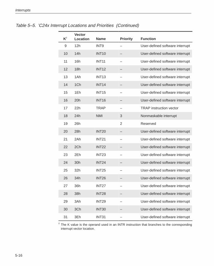
Interrupts
5-16
Table 5–5. ’C24x Interrupt Locations and Priorities (Continued)
ÁÁÁÁÁÁÁÁÁÁÁÁ
K†ÁÁÁÁÁÁÁÁÁÁÁÁ
VectorLocation
ÁÁÁÁÁÁÁÁÁÁÁÁÁÁÁ
NameÁÁÁÁÁÁÁÁÁÁÁÁÁÁÁ
PriorityÁÁÁÁÁÁÁÁÁÁÁÁÁÁÁÁÁÁÁÁÁÁÁÁÁÁÁFunction
9 12h INT9 – User-defined software interrupt
10 14h INT10 – User-defined software interrupt
11 16h INT11 – User-defined software interrupt
12 18h INT12 – User-defined software interrupt
13 1Ah INT13 – User-defined software interrupt
14 1Ch INT14 – User-defined software interrupt
15 1Eh INT15 – User-defined software interrupt
16 20h INT16 – User-defined software interrupt
17 22h TRAP – TRAP instruction vector
18 24h NMI 3 Nonmaskable interrupt
19 26h 2 Reserved
20 28h INT20 – User-defined software interrupt
21 2Ah INT21 – User-defined software interrupt
22 2Ch INT22 – User-defined software interrupt
23 2Eh INT23 – User-defined software interrupt
24 30h INT24 – User-defined software interrupt
25 32h INT25 – User-defined software interrupt
26 34h INT26 – User-defined software interrupt
27 36h INT27 – User-defined software interrupt
28 38h INT28 – User-defined software interrupt
29 3Ah INT29 – User-defined software interrupt
30 3Ch INT30 – User-defined software interrupt
31 3Eh INT31 – User-defined software interrupt
† The K value is the operand used in an INTR instruction that branches to the correspondinginterrupt vector location.
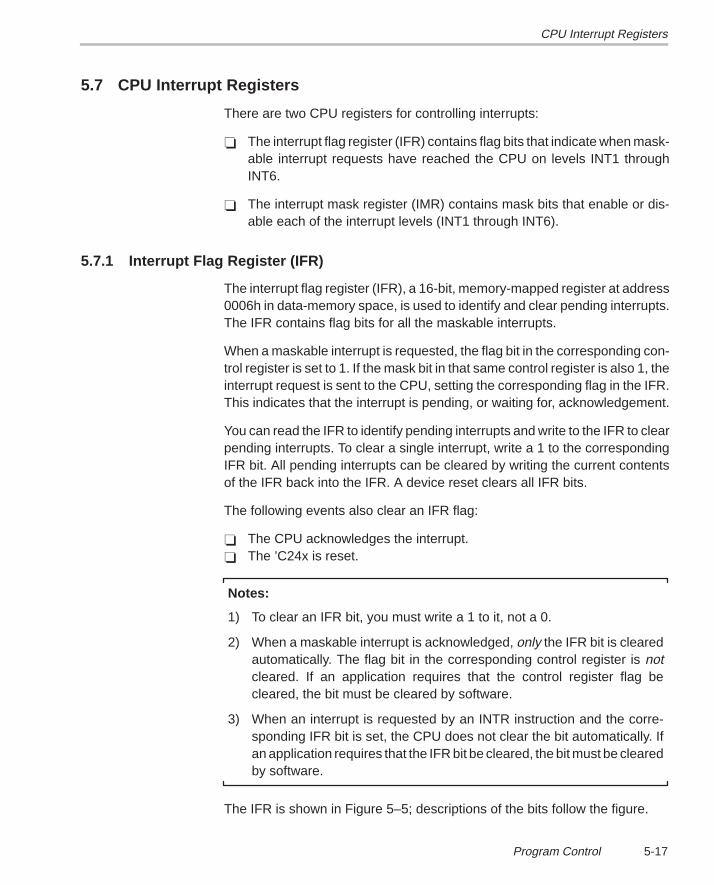
CPU Interrupt Registers
5-17Program Control
5.7 CPU Interrupt Registers
There are two CPU registers for controlling interrupts:
The interrupt flag register (IFR) contains flag bits that indicate when mask-able interrupt requests have reached the CPU on levels INT1 throughINT6.
The interrupt mask register (IMR) contains mask bits that enable or dis-able each of the interrupt levels (INT1 through INT6).
5.7.1 Interrupt Flag Register (IFR)
The interrupt flag register (IFR), a 16-bit, memory-mapped register at address0006h in data-memory space, is used to identify and clear pending interrupts.The IFR contains flag bits for all the maskable interrupts.
When a maskable interrupt is requested, the flag bit in the corresponding con-trol register is set to 1. If the mask bit in that same control register is also 1, theinterrupt request is sent to the CPU, setting the corresponding flag in the IFR.This indicates that the interrupt is pending, or waiting for, acknowledgement.
You can read the IFR to identify pending interrupts and write to the IFR to clearpending interrupts. To clear a single interrupt, write a 1 to the correspondingIFR bit. All pending interrupts can be cleared by writing the current contentsof the IFR back into the IFR. A device reset clears all IFR bits.
The following events also clear an IFR flag:
The CPU acknowledges the interrupt. The ’C24x is reset.
Notes:
1) To clear an IFR bit, you must write a 1 to it, not a 0.
2) When a maskable interrupt is acknowledged, only the IFR bit is clearedautomatically. The flag bit in the corresponding control register is notcleared. If an application requires that the control register flag becleared, the bit must be cleared by software.
3) When an interrupt is requested by an INTR instruction and the corre-sponding IFR bit is set, the CPU does not clear the bit automatically. Ifan application requires that the IFR bit be cleared, the bit must be clearedby software.
The IFR is shown in Figure 5–5; descriptions of the bits follow the figure.
CPU Interrupt Registers
5-18
Figure 5–5. Interrupt Flag Register (IFR) — Address 0006h
15–6 5 4 3 2 1 0
Reserved INT6 INT5 INT4 INT3 INT2 INT1
0 R/W–x R/W1C–x R/W1C–x R/W1C–x R/W1C–x R/W1C–x
Note: 0 = Always read as zeros, R = Read access, W1C = Write 1 to this bit to clear it, –n = Value after reset, x = Value un-changed by reset
Bits 15–6 Reserved . These bits are always read as 0s.
Bit 5 INT6. Interrupt 6 flag. This bit is the flag for interrupts connected to interruptlevel INT6.
0 =No INT6 interrupt is pending.1 =At least one INT6 interrupt is pending. Write a 1 to this bit to clear it to
0 and clear the interrupt request.
Bit 4 INT5. Interrupt 5 flag. This bit is the flag for interrupts connected to interruptlevel INT5.
0 =No INT5 interrupt is pending.1 =At least one INT5 interrupt is pending. Write a 1 to this bit to clear it to
0 and clear the interrupt request.
Bit 3 INT4. Interrupt 4 flag. This bit is the flag for interrupts connected to interruptlevel INT4.
0 =No INT4 interrupt is pending.1 =At least one INT4 interrupt is pending. Write a 1 to this bit to clear it to
0 and clear the interrupt request.
Bit 2 INT3. Interrupt 3 flag. This bit is the flag for interrupts connected to interruptlevel INT3.
0 =No INT3 interrupt is pending.1 =At least one INT3 interrupt is pending. Write a 1 to this bit to clear it to
0 and clear the interrupt request.
Bit 1 INT2. Interrupt 2 flag. This bit is the flag for interrupts connected to interruptlevel INT2.
0 =No INT2 interrupt is pending.1 =At least one INT2 interrupt is pending. Write a 1 to this bit to clear it to
0 and clear the interrupt request.
CPU Interrupt Registers
5-19Program Control
Bit 0 INT1. Interrupt 1 flag. This bit is the flag for interrupts connected to interruptlevel INT1.
0 =No INT1 interrupt is pending.1 =At least one INT1 interrupt is pending. Write a 1 to this bit to clear it to
0 and clear the interrupt request.
5.7.2 Interrupt Mask Register (IMR)
The IMR is a 16-bit, memory-mapped register located at address 0004h indata memory space. The IMR contains mask bits for all the maskable interruptlevels (INT1–INT6). Neither NMI nor RS is included in the IMR; thus, IMR hasno effect on these interrupts.
You can read the IMR to identify masked or unmasked interrupt levels, and youcan write to the IMR to mask or unmask interrupt levels. To unmask an interruptlevel, set its corresponding IMR bit to 1. To mask an interrupt level, set its corre-sponding IMR bit to 0. When an interrupt is masked, it is not acknowledged,regardless of the value of the INTM bit. When an interrupt is unmasked, it isacknowledged if the corresponding IFR bit is 1 and the INTM bit is 0. At reset,the IMR bits are all set to 0, masking all the maskable interrupts.
The IMR is shown in Figure 5–6, Interrupt Mask Register (IMR) on page 5-20.Bit descriptions follow the figure.
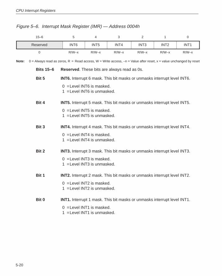
CPU Interrupt Registers
5-20
Figure 5–6. Interrupt Mask Register (IMR) — Address 0004h
15–6 5 4 3 2 1 0
Reserved INT6 INT5 INT4 INT3 INT2 INT1
0 R/W–x R/W–x R/W–x R/W–x R/W–x R/W–x
Note: 0 = Always read as zeros, R = Read access, W = Write access, –n = Value after reset, x = value unchanged by reset
Bits 15–6 Reserved . These bits are always read as 0s.
Bit 5 INT6. Interrupt 6 mask. This bit masks or unmasks interrupt level INT6.
0 =Level INT6 is masked.1 =Level INT6 is unmasked.
Bit 4 INT5. Interrupt 5 mask. This bit masks or unmasks interrupt level INT5.
0 =Level INT5 is masked.1 =Level INT5 is unmasked.
Bit 3 INT4. Interrupt 4 mask. This bit masks or unmasks interrupt level INT4.
0 =Level INT4 is masked.1 =Level INT4 is unmasked.
Bit 2 INT3. Interrupt 3 mask. This bit masks or unmasks interrupt level INT3.
0 =Level INT3 is masked.1 =Level INT3 is unmasked.
Bit 1 INT2. Interrupt 2 mask. This bit masks or unmasks interrupt level INT2.
0 =Level INT2 is masked.1 =Level INT2 is unmasked.
Bit 0 INT1. Interrupt 1 mask. This bit masks or unmasks interrupt level INT1.
0 =Level INT1 is masked.1 =Level INT1 is unmasked.
6-1Addressing Modes
Addressing Modes
This chapter explains the three basic memory addressing modes used by the’C24x instruction set. The three modes are:
Immediate addressing mode Direct addressing mode Indirect addressing mode
In the immediate addressing mode, a constant to be manipulated by theinstruction is supplied directly as an operand of that instruction. The ’C24x sup-ports two types of immediate addressing, long and short, described in section6.1, Immediate Addressing Mode, on page 6-2.
When you need to access data memory, you can use the direct or indirect ad-dressing mode. Direct addressing concatenates seven bits of the instructionword with the nine bits of the data-memory page pointer (DP) to form a 16-bitdata memory address. Indirect addressing accesses data memory throughone of eight 16-bit auxiliary registers.
Topic Page
6.1 Immediate Addressing Mode 6-2. . . . . . . . . . . . . . . . . . . . . . . . . . . . . . . . . . .
6.2 Direct Addressing Mode 6-4. . . . . . . . . . . . . . . . . . . . . . . . . . . . . . . . . . . . . . .
6.3 Indirect Addressing Mode 6-9. . . . . . . . . . . . . . . . . . . . . . . . . . . . . . . . . . . . .
Chapter 6
Immediate Addressing Mode
6-2
6.1 Immediate Addressing Mode
In the immediate addressing mode, the instruction word contains a constantto be manipulated by the instruction. The two types of immediate addressingmodes are:
Short-immediate addressing. Instructions that use short-immediate ad-dressing have an 8-bit, 9-bit, or 13-bit constant as an operand. Short-im-mediate instructions require a single instruction word, with the constantembedded in that word.
Long-immediate addressing. Instructions that use long-immediate ad-dressing have a 16-bit constant as an operand and require two instructionwords. The constant is sent as the second instruction word. This 16-bit val-ue can be used as an absolute constant or as a 2s-complement value.
In Example 6–1, the immediate operand is contained as a part of the RPTinstruction word. For this RPT instruction, the instruction register will be loadedwith the value shown in Figure 6–1. Immediate operands are preceded by thesymbol #.
Example 6–1. RPT Instruction Using Short-Immediate Addressing
RPT #99 ;Execute the instruction that follows RPT;100 times.
Figure 6–1. Instruction Register Contents for Example 6–1
0123456789101112131415
1100011011011101
8-bit constant = 99RPT opcode for immediate addressing
Immediate Addressing Mode
6-3Addressing Modes
In Example 6–2, the immediate operand is contained in the second instructionword. The instruction register receives, consecutively, the two 16-bit valuesshown in Figure 6–2.
Example 6–2. ADD Instruction Using Long-Immediate Addressing
ADD #16384,2 ;Shift the value 16384 left by two bits;and add the result to the accumulator.
Figure 6–2. Two Words Loaded Consecutively to the Instruction Register in Example 6–2
0123456789101112131415
100111111101
shift = 2
16-bit constant = 16384 = 4000h
First instruction word:
Second instruction word:
0100
ADD opcode for long-immediate addressing
000000000010 0000
0123456789101112131415
Direct Addressing Mode
6-4
6.2 Direct Addressing Mode
In the direct addressing mode, data memory is addressed in blocks of 128words called data pages. The entire 64K of data memory consists of 512 datapages labeled 0 through 511, as shown in Figure 6–3. The current data pageis determined by the value in the 9-bit data page pointer (DP) in status registerST0. For example, if the DP value is 0 0000 00002, the current data page is0. If the DP value is 0 0000 00102, the current data page is 2.
Figure 6–3. Pages of Data Memory
1111 1111 1
0000 0000 1
0000 0001 0
0000 0001 0
0000 0000 0
Data Memory
Page 0: 0000h–007Fh
Page 1: 0080h–00FFh
Page 2: 0100h–017Fh
Page 511: FF80h–FFFFh
.
000 0000
OffsetDP Value
0000 0000 0
111 11110000 0000 1
1111 1111 1
000 0000
111 1111
000 0000
111 1111
000 0000
111 1111
.
.
.
.
.
.
.
.
.
.
.
.
.
.
.
.
.
.
..
.
..
.
..
. ...
..
.
..
.
..
. ...
In addition to the data page, the processor must know the particular word beingreferenced on that page. This is determined by a 7-bit offset (see Figure 6–3).The offset is supplied by the seven least significant bits (LSBs) of the IR regis-ter shown in Figure 6–4, Instruction Register (IR) Contents in Direct Address-ing Mode instruction register, on page 6-5, which holds the opcode for thenext instruction to be executed. In direct addressing mode, the contents of theinstruction register has the format.
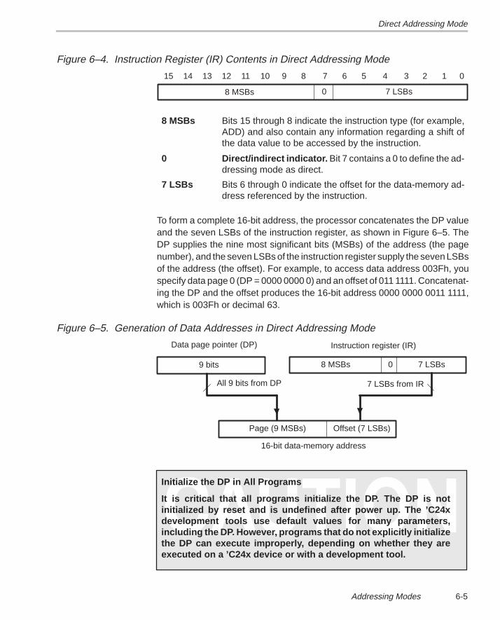
Direct Addressing Mode
6-5Addressing Modes
Figure 6–4. Instruction Register (IR) Contents in Direct Addressing Mode
0123456789101112131415
7 LSBs08 MSBs
8 MSBs Bits 15 through 8 indicate the instruction type (for example,ADD) and also contain any information regarding a shift ofthe data value to be accessed by the instruction.
0 Direct/indirect indicator. Bit 7 contains a 0 to define the ad-dressing mode as direct.
7 LSBs Bits 6 through 0 indicate the offset for the data-memory ad-dress referenced by the instruction.
To form a complete 16-bit address, the processor concatenates the DP valueand the seven LSBs of the instruction register, as shown in Figure 6–5. TheDP supplies the nine most significant bits (MSBs) of the address (the pagenumber), and the seven LSBs of the instruction register supply the seven LSBsof the address (the offset). For example, to access data address 003Fh, youspecify data page 0 (DP = 0000 0000 0) and an offset of 011 1111. Concatenat-ing the DP and the offset produces the 16-bit address 0000 0000 0011 1111,which is 003Fh or decimal 63.
Figure 6–5. Generation of Data Addresses in Direct Addressing Mode
7 LSBs from IR
16-bit data-memory address
All 9 bits from DP
Data page pointer (DP)
Page (9 MSBs) Offset (7 LSBs)
Instruction register (IR)
8 MSBs 7 LSBs9 bits 0
Initialize the DP in All Programs
It is critical that all programs initialize the DP. The DP is notinitialized by reset and is undefined after power up. The ’C24xdevelopment tools use default values for many parameters,including the DP. However, programs that do not explicitly initializethe DP can execute improperly, depending on whether they areexecuted on a ’C24x device or with a development tool.
Direct Addressing Mode
6-6
6.2.1 Using Direct Addressing Mode
When you use direct addressing mode, the processor uses the DP to find thedata page and uses the seven LSBs of the instruction register to find a particu-lar address on that page. Always do the following:
1) Set the data page. Load the appropriate value (from 0 to 511) into the DP.The DP register can be loaded by the LDP instruction or by any instructionthat can load a value to ST0. The LDP instruction loads the DP directlywithout affecting the other bits of ST0, and it clearly indicates the valueloaded into the DP. For example, to set the current data page to 32 (ad-dresses 1000h–107Fh), you can use:
LDP #32 ;Initialize data page pointer
2) Specify the offset. Supply the 7-bit offset as an operand of the instruction.For example, if you want the ADD instruction to use the value at the secondaddress of the current data page, you would write:
ADD 1h ;Add to accumulator the value in the current;data page, offset of 1.
You do not have to set the data page prior to every instruction that uses directaddressing. If all the instructions in a block of code access the same data page,you can simply load the DP at the front of the block. However, if various datapages are being accessed throughout the block of code, be sure the DP ischanged whenever a new data page should be accessed.
6.2.2 Examples of Direct Addressing
In Example 6–3, the first instruction loads the DP with 0 0000 01002 to set thecurrent data page to 4. The ADD instruction then references a data memoryaddress that is generated as shown following the program code. Before theADD instruction is executed, the opcode is loaded into the instruction register.Together, the DP and the seven LSBs of the instruction register form the com-plete 16-bit address, 0000 0010 0000 10012 (0209h).
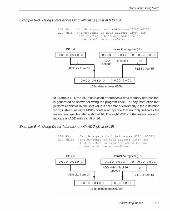
Direct Addressing Mode
6-7Addressing Modes
Example 6–3. Using Direct Addressing with ADD (Shift of 0 to 15)
LDP #4 ;Set data page to 4 (addresses 0200h–027Fh).ADD 9h,5 ;The contents of data address 0209h are
;left shifted 5 bits and added to the;contents of the accumulator.
7 LSBs from IR
16-bit data address 0209h
All 9 bits from DP
DP = 4 Instruction register (IR)
0 0 1 0 0 0 0 1 0 0 10 0 0 0 0 0 1 0 0 00 0 1 0
ADDopcode
Shift of 5
0 0 0 0 0 0 1 0 0 0 0 0 1 0 0 1
9h
In Example 6–4, the ADD instruction references a data memory address thatis generated as shown following the program code. For any instruction thatperforms a shift of 16, the shift value is not embedded directly in the instructionword; instead, all eight MSBs contain an opcode that not only indicates theinstruction type, but also a shift of 16. The eight MSBs of the instruction wordindicate an ADD with a shift of 16.
Example 6–4. Using Direct Addressing with ADD (Shift of 16)
LDP #5 ;Set data page to 5 (addresses 0280h–02FFh).ADD 9h,16 ;The contents of data address 0289h are
;left shifted 16 bits and added to the;contents of the accumulator.
7 LSBs from IR
16-bit data address 0289h
All 9 bits from DP
DP = 5 Instruction register (IR)
0 0 0 1 0 0 10 0 0 0 0 0 1 0 1 0
ADD with shift of 16opcode
0 0 0 0 0 0 1 0 1 0 0 0 1 0 0 1
9h
0 1 1 0 0 0 0 1
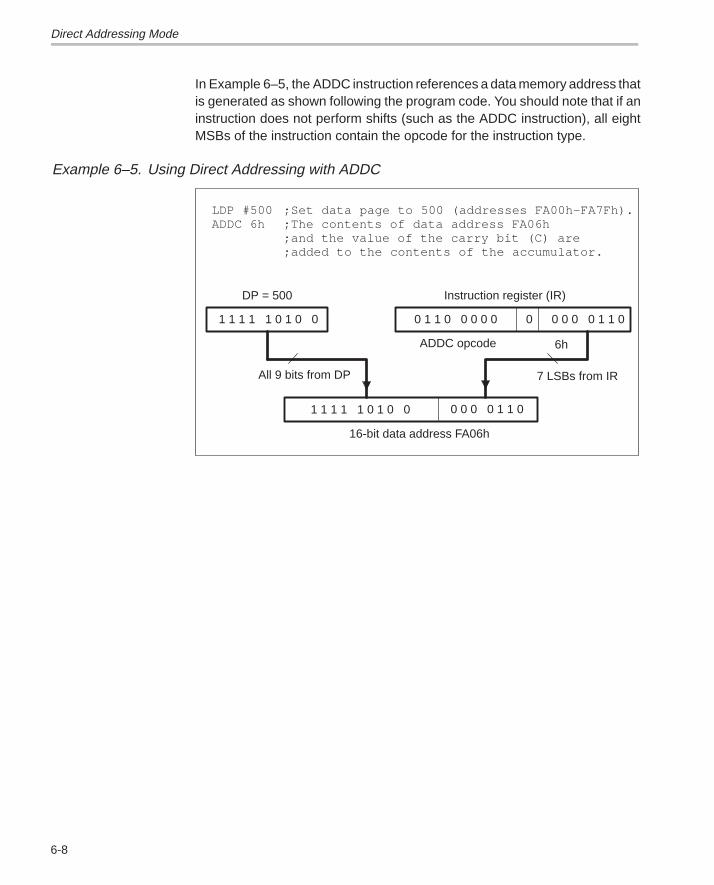
Direct Addressing Mode
6-8
In Example 6–5, the ADDC instruction references a data memory address thatis generated as shown following the program code. You should note that if aninstruction does not perform shifts (such as the ADDC instruction), all eightMSBs of the instruction contain the opcode for the instruction type.
Example 6–5. Using Direct Addressing with ADDC
LDP #500 ;Set data page to 500 (addresses FA00h–FA7Fh).ADDC 6h ;The contents of data address FA06h ;and the value of the carry bit (C) are
;added to the contents of the accumulator.
7 LSBs from IR
16-bit data address FA06h
All 9 bits from DP
DP = 500 Instruction register (IR)
0 0 0 0 1 1 01 1 1 1 1 0 1 0 0 0
ADDC opcode
1 1 1 1 1 0 1 0 0 0 0 0 0 1 1 0
6h
0 1 1 0 0 0 0 0
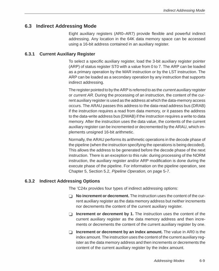
Indirect Addressing Mode
6-9Addressing Modes
6.3 Indirect Addressing Mode
Eight auxiliary registers (AR0–AR7) provide flexible and powerful indirectaddressing. Any location in the 64K data memory space can be accessedusing a 16-bit address contained in an auxiliary register.
6.3.1 Current Auxiliary Register
To select a specific auxiliary register, load the 3-bit auxiliary register pointer(ARP) of status register ST0 with a value from 0 to 7. The ARP can be loadedas a primary operation by the MAR instruction or by the LST instruction. TheARP can be loaded as a secondary operation by any instruction that supportsindirect addressing.
The register pointed to by the ARP is referred to as the current auxiliary registeror current AR. During the processing of an instruction, the content of the cur-rent auxiliary register is used as the address at which the data-memory accessoccurs. The ARAU passes this address to the data-read address bus (DRAB)if the instruction requires a read from data memory, or it passes the addressto the data-write address bus (DWAB) if the instruction requires a write to datamemory. After the instruction uses the data value, the contents of the currentauxiliary register can be incremented or decremented by the ARAU, which im-plements unsigned 16-bit arithmetic.
Normally, the ARAU performs its arithmetic operations in the decode phase ofthe pipeline (when the instruction specifying the operations is being decoded).This allows the address to be generated before the decode phase of the nextinstruction. There is an exception to this rule: during processing of the NORMinstruction, the auxiliary register and/or ARP modification is done during theexecute phase of the pipeline. For information on the pipeline operation, seeChapter 5, Section 5.2, Pipeline Operation, on page 5-7.
6.3.2 Indirect Addressing Options
The ’C24x provides four types of indirect addressing options:
No increment or decrement. The instruction uses the content of the cur-rent auxiliary register as the data memory address but neither incrementsnor decrements the content of the current auxiliary register.
Increment or decrement by 1. The instruction uses the content of thecurrent auxiliary register as the data memory address and then incre-ments or decrements the content of the current auxiliary register by one.
Increment or decrement by an index amount. The value in AR0 is theindex amount. The instruction uses the content of the current auxiliary reg-ister as the data memory address and then increments or decrements thecontent of the current auxiliary register by the index amount.
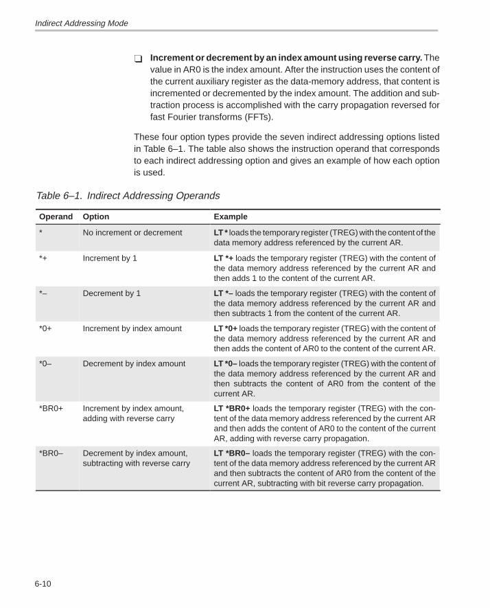
Indirect Addressing Mode
6-10
Increment or decrement by an index amount using reverse carry. Thevalue in AR0 is the index amount. After the instruction uses the content ofthe current auxiliary register as the data-memory address, that content isincremented or decremented by the index amount. The addition and sub-traction process is accomplished with the carry propagation reversed forfast Fourier transforms (FFTs).
These four option types provide the seven indirect addressing options listedin Table 6–1. The table also shows the instruction operand that correspondsto each indirect addressing option and gives an example of how each optionis used.
Table 6–1. Indirect Addressing Operands
Operand Option Example
* No increment or decrement LT * loads the temporary register (TREG) with the content of thedata memory address referenced by the current AR.
*+ Increment by 1 LT *+ loads the temporary register (TREG) with the content ofthe data memory address referenced by the current AR andthen adds 1 to the content of the current AR.
*– Decrement by 1 LT *– loads the temporary register (TREG) with the content ofthe data memory address referenced by the current AR andthen subtracts 1 from the content of the current AR.
*0+ Increment by index amount LT *0+ loads the temporary register (TREG) with the content ofthe data memory address referenced by the current AR andthen adds the content of AR0 to the content of the current AR.
*0– Decrement by index amount LT *0– loads the temporary register (TREG) with the content ofthe data memory address referenced by the current AR andthen subtracts the content of AR0 from the content of thecurrent AR.
*BR0+ Increment by index amount,adding with reverse carry
LT *BR0+ loads the temporary register (TREG) with the con-tent of the data memory address referenced by the current ARand then adds the content of AR0 to the content of the currentAR, adding with reverse carry propagation.
*BR0– Decrement by index amount,subtracting with reverse carry
LT *BR0– loads the temporary register (TREG) with the con-tent of the data memory address referenced by the current ARand then subtracts the content of AR0 from the content of thecurrent AR, subtracting with bit reverse carry propagation.
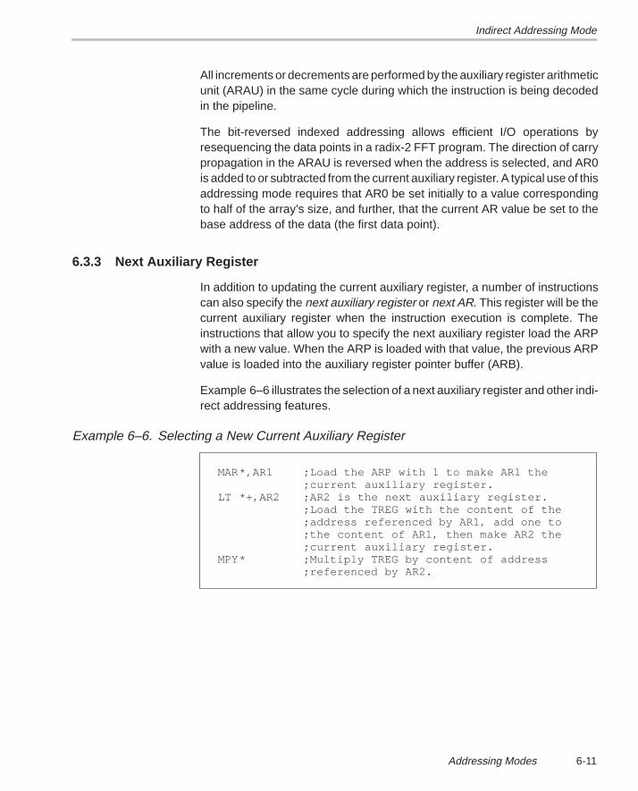
Indirect Addressing Mode
6-11Addressing Modes
All increments or decrements are performed by the auxiliary register arithmeticunit (ARAU) in the same cycle during which the instruction is being decodedin the pipeline.
The bit-reversed indexed addressing allows efficient I/O operations byresequencing the data points in a radix-2 FFT program. The direction of carrypropagation in the ARAU is reversed when the address is selected, and AR0is added to or subtracted from the current auxiliary register. A typical use of thisaddressing mode requires that AR0 be set initially to a value correspondingto half of the array’s size, and further, that the current AR value be set to thebase address of the data (the first data point).
6.3.3 Next Auxiliary Register
In addition to updating the current auxiliary register, a number of instructionscan also specify the next auxiliary register or next AR. This register will be thecurrent auxiliary register when the instruction execution is complete. Theinstructions that allow you to specify the next auxiliary register load the ARPwith a new value. When the ARP is loaded with that value, the previous ARPvalue is loaded into the auxiliary register pointer buffer (ARB).
Example 6–6 illustrates the selection of a next auxiliary register and other indi-rect addressing features.
Example 6–6. Selecting a New Current Auxiliary Register
MAR*,AR1 ;Load the ARP with 1 to make AR1 the;current auxiliary register.
LT *+,AR2 ;AR2 is the next auxiliary register.;Load the TREG with the content of the;address referenced by AR1, add one to;the content of AR1, then make AR2 the;current auxiliary register.
MPY* ;Multiply TREG by content of address;referenced by AR2.
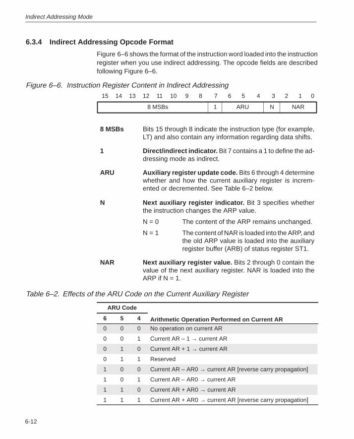
Indirect Addressing Mode
6-12
6.3.4 Indirect Addressing Opcode Format
Figure 6–6 shows the format of the instruction word loaded into the instructionregister when you use indirect addressing. The opcode fields are describedfollowing Figure 6–6.
Figure 6–6. Instruction Register Content in Indirect Addressing0123456789101112131415
NARNARU18 MSBs
8 MSBs Bits 15 through 8 indicate the instruction type (for example,LT) and also contain any information regarding data shifts.
1 Direct/indirect indicator. Bit 7 contains a 1 to define the ad-dressing mode as indirect.
ARU Auxiliary register update code. Bits 6 through 4 determinewhether and how the current auxiliary register is increm-ented or decremented. See Table 6–2 below.
N Next auxiliary register indicator. Bit 3 specifies whetherthe instruction changes the ARP value.
N = 0 The content of the ARP remains unchanged.
N = 1 The content of NAR is loaded into the ARP, andthe old ARP value is loaded into the auxiliaryregister buffer (ARB) of status register ST1.
NAR Next auxiliary register value. Bits 2 through 0 contain thevalue of the next auxiliary register. NAR is loaded into theARP if N = 1.
Table 6–2. Effects of the ARU Code on the Current Auxiliary Register
ARU Code
6 5 4 Arithmetic Operation Performed on Current AR
0 0 0 No operation on current AR
0 0 1 Current AR – 1 → current AR
0 1 0 Current AR + 1 → current AR
0 1 1 Reserved
1 0 0 Current AR – AR0 → current AR [reverse carry propagation]
1 0 1 Current AR – AR0 → current AR
1 1 0 Current AR + AR0 → current AR
1 1 1 Current AR + AR0 → current AR [reverse carry propagation]
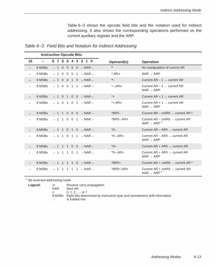
Indirect Addressing Mode
6-13Addressing Modes
Table 6–3 shows the opcode field bits and the notation used for indirectaddressing. It also shows the corresponding operations performed on thecurrent auxiliary register and the ARP.
Table 6–3. Field Bits and Notation for Indirect Addressing
Instruction Opcode Bits
15 – 8 7 6 5 4 3 2 1 0 Operand(s) Operation
← 8 MSBs → 1 0 0 0 0 ←NAR→ * No manipulation of current AR
← 8 MSBs → 1 0 0 0 1 ←NAR→ *,ARn NAR → ARP
← 8 MSBs → 1 0 0 1 0 ←NAR→ *– Current AR – 1 → current AR
← 8 MSBs → 1 0 0 1 1 ←NAR→ *–,ARn Current AR – 1 → current ARNAR → ARP
← 8 MSBs → 1 0 1 0 0 ←NAR→ *+ Current AR + 1 → current AR
← 8 MSBs → 1 0 1 0 1 ←NAR→ *+,ARn Current AR + 1 → current ARNAR → ARP
← 8 MSBs → 1 1 0 0 0 ←NAR→ *BR0– Current AR – rcAR0 → current AR †
← 8 MSBs → 1 1 0 0 1 ←NAR→ *BR0–,ARn Current AR – rcAR0 → current ARNAR → ARP †
← 8 MSBs → 1 1 0 1 0 ←NAR→ *0– Current AR – AR0 → current AR
← 8 MSBs → 1 1 0 1 1 ←NAR→ *0–,ARn Current AR – AR0 → current ARNAR → ARP
← 8 MSBs → 1 1 1 0 0 ←NAR→ *0+ Current AR + AR0 → current AR
← 8 MSBs → 1 1 1 0 1 ←NAR→ *0+,ARn Current AR + AR0 → current ARNAR → ARP
← 8 MSBs → 1 1 1 1 0 ←NAR→ *BR0+ Current AR + rcAR0 → current AR †
← 8 MSBs → 1 1 1 1 1 ←NAR→ *BR0+,ARn Current AR + rcAR0 → current ARNAR → ARP †
† Bit-reversed addressing mode
Legend: rc Reverse carry propagationNAR Next ARn 0, 1, 2, ..., or 78 MSBs Eight bits determined by instruction type and (sometimes) shift information→ Is loaded into
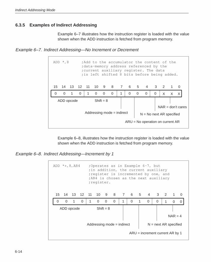
Indirect Addressing Mode
6-14
6.3.5 Examples of Indirect Addressing
Example 6–7 illustrates how the instruction register is loaded with the valueshown when the ADD instruction is fetched from program memory.
Example 6–7. Indirect Addressing—No Increment or Decrement
ADD *,8 ;Add to the accumulator the content of the;data-memory address referenced by the;current auxiliary register. The data;is left shifted 8 bits before being added.
0123456789101112131415
N = No next AR specified
ARU = No operation on current AR
1
Shift = 8
0 0 0 0 X X X
ADD opcode
0 0 1 0 1 0 0 0
Addressing mode = indirect
NAR = don’t cares
Example 6–8, illustrates how the instruction register is loaded with the valueshown when the ADD instruction is fetched from program memory.
Example 6–8. Indirect Addressing—Increment by 1
ADD *+,8,AR4 ;Operates as in Example 6–7, but;in addition, the current auxiliary;register is incremented by one, and;AR4 is chosen as the next auxiliary;register.
0123456789101112131415
NAR = 4
N = next AR specified
ARU = increment current AR by 1
1
Shift = 8
0 1 0 0 1 0 0
ADD opcode
0 0 1 0 1 0 0 0
Addressing mode = indirect
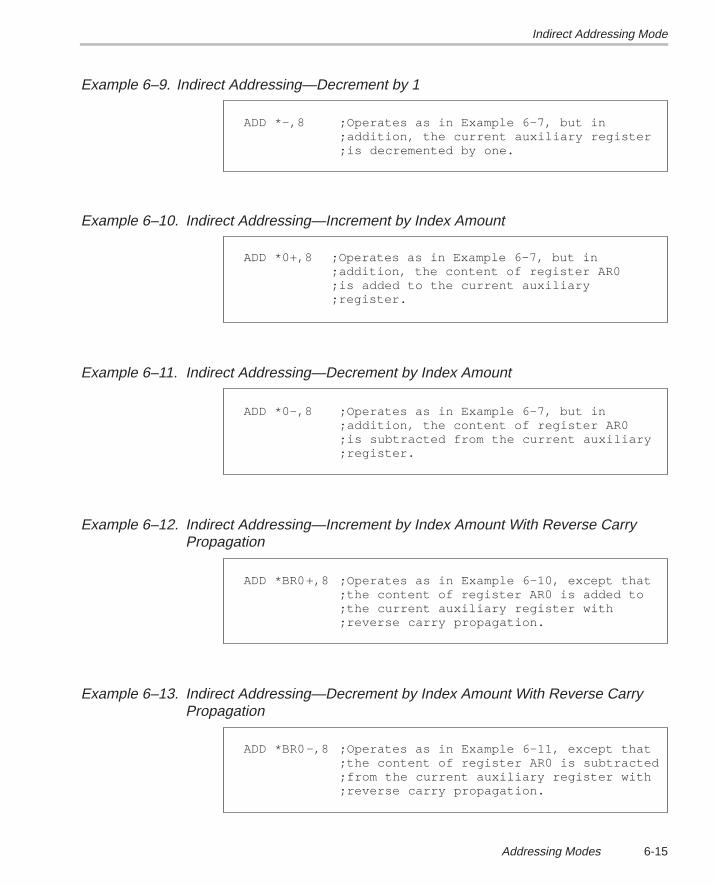
Indirect Addressing Mode
6-15Addressing Modes
Example 6–9. Indirect Addressing—Decrement by 1
ADD *–,8 ;Operates as in Example 6–7, but in;addition, the current auxiliary register;is decremented by one.
Example 6–10. Indirect Addressing—Increment by Index Amount
ADD *0+,8 ;Operates as in Example 6–7, but in;addition, the content of register AR0;is added to the current auxiliary;register.
Example 6–11. Indirect Addressing—Decrement by Index Amount
ADD *0–,8 ;Operates as in Example 6–7, but in;addition, the content of register AR0;is subtracted from the current auxiliary;register.
Example 6–12. Indirect Addressing—Increment by Index Amount With Reverse CarryPropagation
ADD *BR0+,8 ;Operates as in Example 6–10, except that;the content of register AR0 is added to;the current auxiliary register with;reverse carry propagation.
Example 6–13. Indirect Addressing—Decrement by Index Amount With Reverse CarryPropagation
ADD *BR0–,8 ;Operates as in Example 6–11, except that;the content of register AR0 is subtracted;from the current auxiliary register with;reverse carry propagation.
Indirect Addressing Mode
6-16
6.3.6 Modifying Auxiliary Register Content
The LAR, ADRK, SBRK, and MAR instructions are specialized instructions forchanging the content of an auxiliary register (AR):
The LAR instruction loads an AR.
The ADRK instruction adds an immediate value to an AR; SBRK subtractsan immediate value.
The MAR instruction can increment or decrement an AR value by 1 or byan index amount.
When modifying auxiliary register content, you are not limited to these fourinstructions. Auxiliary registers can be modified by any instruction that sup-ports indirect addressing operands. (Indirect addressing can be used with allinstructions except those that have immediate operands or no operands.)
7-1Assembly Language Instructions
Assembly Language Instructions
Note:
The instruction set for the TMS320C24x is identical to that of theTMS320C2xx core.
This chapter describes the ’C24x assembly language instructions. Thisinstruction set supports numerically intensive signal-processing operations aswell as general-purpose applications, such as multiprocessing and high-speed control. The ’C24x instruction set is compatible with the ’C2x instructionset; code written for the ’C2x can be reassembled to run on the ’C24x. The ’C5xinstruction set is a superset of that of the ’C24x; thus, code written for the ’C24xcan be upgraded to run on a ’C5x.
Topic Page
7.1 Instruction Set Summary 7-2. . . . . . . . . . . . . . . . . . . . . . . . . . . . . . . . . . . . . .
7.2 How To Use the Instruction Descriptions 7-12. . . . . . . . . . . . . . . . . . . . . . .
7.3 Instruction Descriptions 7-19. . . . . . . . . . . . . . . . . . . . . . . . . . . . . . . . . . . . . .
Chapter 7
Instruction Set Summary
7-2
7.1 Instruction Set Summary
This section provides six tables (Table 7–1 to Table 7–6) that summarize theinstruction set according to the following functional headings:
Accumulator, arithmetic, and logic instructions (see Table 7–1 on page7-5)
Auxiliary register and data page pointer instructions (see Table 7–2 onpage 7-7)
TREG, PREG, and multiply instructions (see Table 7–3 on page 7-8)
Branch instructions (see Table 7–4 on page 7-9)
Control instructions (see Table 7–5 on page 7-10)
I/O and memory operations (see Table 7–6 on page 7-11)
Within each table, the instructions are arranged alphabetically. The number ofwords that an instruction occupies in program memory is specified in columnthree of each table; the number of cycles that an instruction requires to executeis in column four. All instructions are assumed to be executed from internalprogram memory (RAM) and internal data dual-access memory. The cycletimings are for single-instruction execution, not for repeat mode. Additionalinformation about each instruction is presented in the individual instructiondescriptions in Section 7.2 on page 7-12.
For your reference, here are the definitions of the symbols used in the sixsummary tables:
ACC The accumulator
AR The auxiliary register
ARX A 3-bit value used in the LAR and SAR instructions to desig-nate which auxiliary register will be loaded (LAR) or have itscontents stored (SAR)
BITX A 4-bit value (called the bit code) that determines which bit ofa designated data memory value will be tested by the BITinstruction
CM A 2-bit value. The CMPR instruction performs a comparisonspecified by the value of CM:
If CM = 00, test whether current AR = AR0If CM = 01, test whether current AR < AR0If CM = 10, test whether current AR > AR0If CM = 11, test whether current AR ≠ AR0
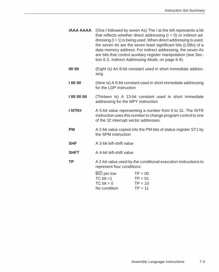
Instruction Set Summary
7-3Assembly Language Instructions
IAAA AAAA (One I followed by seven As) The I at the left represents a bitthat reflects whether direct addressing (I = 0) or indirect ad-dressing (I = 1) is being used. When direct addressing is used,the seven As are the seven least significant bits (LSBs) of adata memory address. For indirect addressing, the seven Asare bits that control auxiliary register manipulation (see Sec-tion 6.3, Indirect Addressing Mode, on page 6-9).
IIII IIII (Eight Is) An 8-bit constant used in short immediate addres-sing
I IIII IIII (Nine Is) A 9-bit constant used in short immediate addressingfor the LDP instruction
I IIII IIII IIII (Thirteen Is) A 13-bit constant used in short immediateaddressing for the MPY instruction
I NTR# A 5-bit value representing a number from 0 to 31. The INTRinstruction uses this number to change program control to oneof the 32 interrupt vector addresses.
PM A 2-bit value copied into the PM bits of status register ST1 bythe SPM instruction
SHF A 3-bit left-shift value
SHFT A 4-bit left-shift value
TP A 2-bit value used by the conditional execution instructions torepresent four conditions:
BIO pin low TP = 00TC bit =1 TP = 01TC bit = 0 TP = 10No condition TP = 11
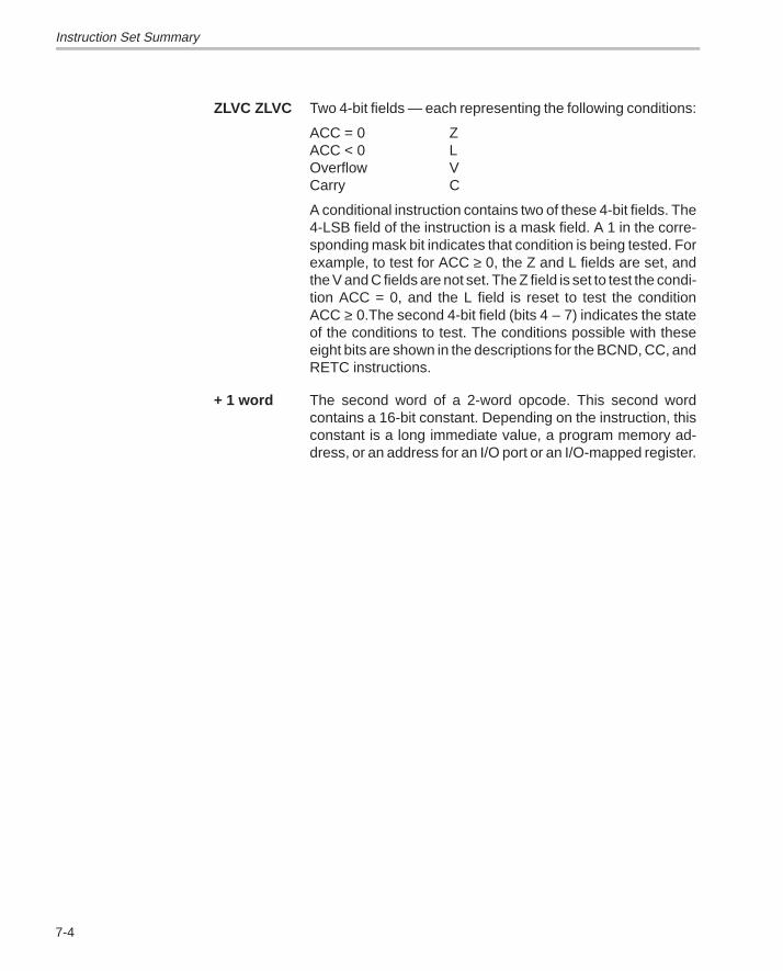
Instruction Set Summary
7-4
ZLVC ZLVC Two 4-bit fields — each representing the following conditions:
ACC = 0 ZACC < 0 LOverflow VCarry C
A conditional instruction contains two of these 4-bit fields. The4-LSB field of the instruction is a mask field. A 1 in the corre-sponding mask bit indicates that condition is being tested. Forexample, to test for ACC ≥ 0, the Z and L fields are set, andthe V and C fields are not set. The Z field is set to test the condi-tion ACC = 0, and the L field is reset to test the conditionACC ≥ 0.The second 4-bit field (bits 4 – 7) indicates the stateof the conditions to test. The conditions possible with theseeight bits are shown in the descriptions for the BCND, CC, andRETC instructions.
+ 1 word The second word of a 2-word opcode. This second wordcontains a 16-bit constant. Depending on the instruction, thisconstant is a long immediate value, a program memory ad-dress, or an address for an I/O port or an I/O-mapped register.
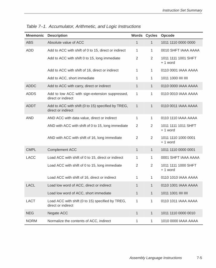
Instruction Set Summary
7-5Assembly Language Instructions
Table 7–1. Accumulator, Arithmetic, and Logic Instructions
Mnemonic Description Words Cycles Opcode
ABS Absolute value of ACC 1 1 1011 1110 0000 0000
ADD Add to ACC with shift of 0 to 15, direct or indirect 1 1 0010 SHFT IAAA AAAA
Add to ACC with shift 0 to 15, long immediate 2 2 1011 1111 1001 SHFT+ 1 word
Add to ACC with shift of 16, direct or indirect 1 1 0110 0001 IAAA AAAA
Add to ACC, short immediate 1 1 1011 1000 IIII IIII
ADDC Add to ACC with carry, direct or indirect 1 1 0110 0000 IAAA AAAA
ADDS Add to low ACC with sign-extension suppressed,direct or indirect
1 1 0110 0010 IAAA AAAA
ADDT Add to ACC with shift (0 to 15) specified by TREG,direct or indirect
1 1 0110 0011 IAAA AAAA
AND AND ACC with data value, direct or indirect 1 1 0110 1110 IAAA AAAA
AND with ACC with shift of 0 to 15, long immediate 2 2 1011 1111 1011 SHFT+ 1 word
AND with ACC with shift of 16, long immediate 2 2 1011 1110 1000 0001+ 1 word
CMPL Complement ACC 1 1 1011 1110 0000 0001
LACC Load ACC with shift of 0 to 15, direct or indirect 1 1 0001 SHFT IAAA AAAA
Load ACC with shift of 0 to 15, long immediate 2 2 1011 1111 1000 SHFT+ 1 word
Load ACC with shift of 16, direct or indirect 1 1 0110 1010 IAAA AAAA
LACL Load low word of ACC, direct or indirect 1 1 0110 1001 IAAA AAAA
Load low word of ACC, short immediate 1 1 1011 1001 IIII IIII
LACT Load ACC with shift (0 to 15) specified by TREG,direct or indirect
1 1 0110 1011 IAAA AAAA
NEG Negate ACC 1 1 1011 1110 0000 0010
NORM Normalize the contents of ACC, indirect 1 1 1010 0000 IAAA AAAA
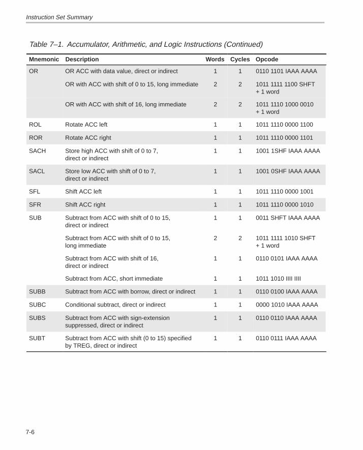
Instruction Set Summary
7-6
Table 7–1. Accumulator, Arithmetic, and Logic Instructions (Continued)
Mnemonic OpcodeCyclesWordsDescription
OR OR ACC with data value, direct or indirect 1 1 0110 1101 IAAA AAAA
OR with ACC with shift of 0 to 15, long immediate 2 2 1011 1111 1100 SHFT+ 1 word
OR with ACC with shift of 16, long immediate 2 2 1011 1110 1000 0010+ 1 word
ROL Rotate ACC left 1 1 1011 1110 0000 1100
ROR Rotate ACC right 1 1 1011 1110 0000 1101
SACH Store high ACC with shift of 0 to 7,direct or indirect
1 1 1001 1SHF IAAA AAAA
SACL Store low ACC with shift of 0 to 7,direct or indirect
1 1 1001 0SHF IAAA AAAA
SFL Shift ACC left 1 1 1011 1110 0000 1001
SFR Shift ACC right 1 1 1011 1110 0000 1010
SUB Subtract from ACC with shift of 0 to 15,direct or indirect
1 1 0011 SHFT IAAA AAAA
Subtract from ACC with shift of 0 to 15,long immediate
2 2 1011 1111 1010 SHFT+ 1 word
Subtract from ACC with shift of 16,direct or indirect
1 1 0110 0101 IAAA AAAA
Subtract from ACC, short immediate 1 1 1011 1010 IIII IIII
SUBB Subtract from ACC with borrow, direct or indirect 1 1 0110 0100 IAAA AAAA
SUBC Conditional subtract, direct or indirect 1 1 0000 1010 IAAA AAAA
SUBS Subtract from ACC with sign-extensionsuppressed, direct or indirect
1 1 0110 0110 IAAA AAAA
SUBT Subtract from ACC with shift (0 to 15) specifiedby TREG, direct or indirect
1 1 0110 0111 IAAA AAAA
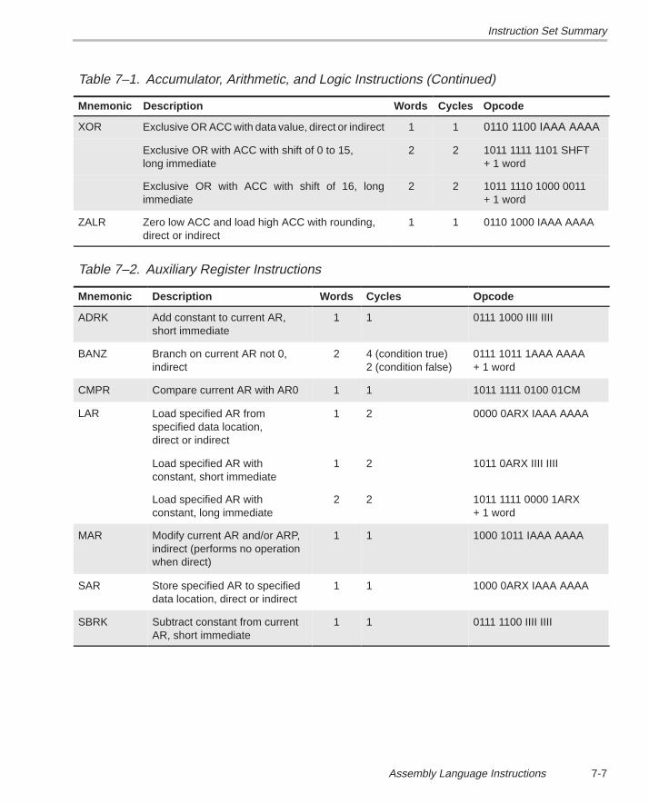
Instruction Set Summary
7-7Assembly Language Instructions
Table 7–1. Accumulator, Arithmetic, and Logic Instructions (Continued)
Mnemonic OpcodeCyclesWordsDescription
XOR Exclusive OR ACC with data value, direct or indirect 1 1 0110 1100 IAAA AAAA
Exclusive OR with ACC with shift of 0 to 15,long immediate
2 2 1011 1111 1101 SHFT+ 1 word
Exclusive OR with ACC with shift of 16, longimmediate
2 2 1011 1110 1000 0011+ 1 word
ZALR Zero low ACC and load high ACC with rounding,direct or indirect
1 1 0110 1000 IAAA AAAA
Table 7–2. Auxiliary Register Instructions
Mnemonic Description Words Cycles Opcode
ADRK Add constant to current AR,short immediate
1 1 0111 1000 IIII IIII
BANZ Branch on current AR not 0,indirect
2 4 (condition true)2 (condition false)
0111 1011 1AAA AAAA+ 1 word
CMPR Compare current AR with AR0 1 1 1011 1111 0100 01CM
LAR Load specified AR fromspecified data location,direct or indirect
1 2 0000 0ARX IAAA AAAA
Load specified AR withconstant, short immediate
1 2 1011 0ARX IIII IIII
Load specified AR withconstant, long immediate
2 2 1011 1111 0000 1ARX+ 1 word
MAR Modify current AR and/or ARP,indirect (performs no operationwhen direct)
1 1 1000 1011 IAAA AAAA
SAR Store specified AR to specifieddata location, direct or indirect
1 1 1000 0ARX IAAA AAAA
SBRK Subtract constant from currentAR, short immediate
1 1 0111 1100 IIII IIII
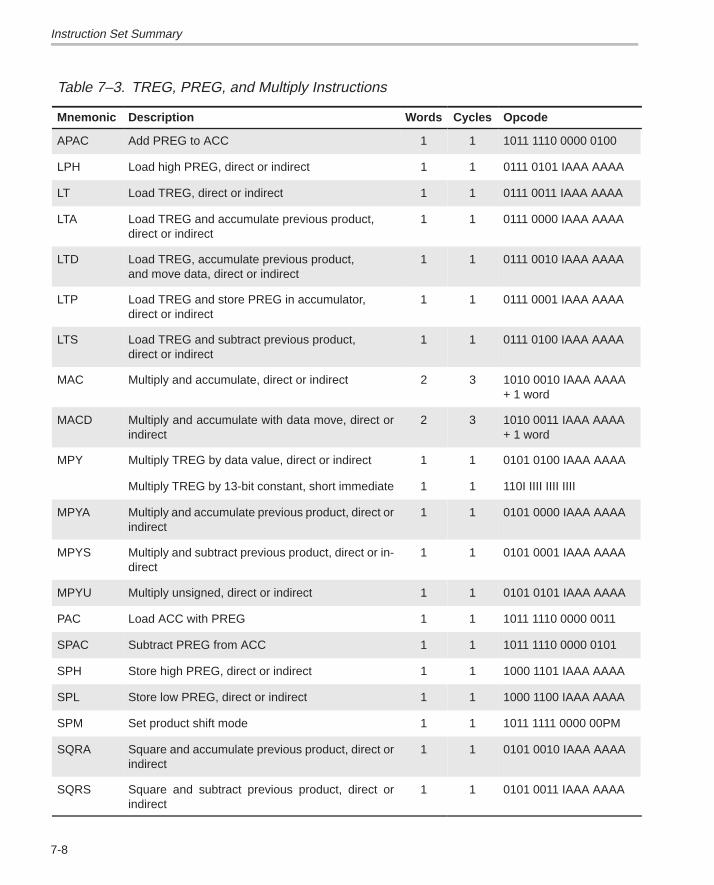
Instruction Set Summary
7-8
Table 7–3. TREG, PREG, and Multiply Instructions
Mnemonic Description Words Cycles Opcode
APAC Add PREG to ACC 1 1 1011 1110 0000 0100
LPH Load high PREG, direct or indirect 1 1 0111 0101 IAAA AAAA
LT Load TREG, direct or indirect 1 1 0111 0011 IAAA AAAA
LTA Load TREG and accumulate previous product,direct or indirect
1 1 0111 0000 IAAA AAAA
LTD Load TREG, accumulate previous product,and move data, direct or indirect
1 1 0111 0010 IAAA AAAA
LTP Load TREG and store PREG in accumulator,direct or indirect
1 1 0111 0001 IAAA AAAA
LTS Load TREG and subtract previous product,direct or indirect
1 1 0111 0100 IAAA AAAA
MAC Multiply and accumulate, direct or indirect 2 3 1010 0010 IAAA AAAA+ 1 word
MACD Multiply and accumulate with data move, direct orindirect
2 3 1010 0011 IAAA AAAA+ 1 word
MPY Multiply TREG by data value, direct or indirect 1 1 0101 0100 IAAA AAAA
Multiply TREG by 13-bit constant, short immediate 1 1 110I IIII IIII IIII
MPYA Multiply and accumulate previous product, direct orindirect
1 1 0101 0000 IAAA AAAA
MPYS Multiply and subtract previous product, direct or in-direct
1 1 0101 0001 IAAA AAAA
MPYU Multiply unsigned, direct or indirect 1 1 0101 0101 IAAA AAAA
PAC Load ACC with PREG 1 1 1011 1110 0000 0011
SPAC Subtract PREG from ACC 1 1 1011 1110 0000 0101
SPH Store high PREG, direct or indirect 1 1 1000 1101 IAAA AAAA
SPL Store low PREG, direct or indirect 1 1 1000 1100 IAAA AAAA
SPM Set product shift mode 1 1 1011 1111 0000 00PM
SQRA Square and accumulate previous product, direct orindirect
1 1 0101 0010 IAAA AAAA
SQRS Square and subtract previous product, direct orindirect
1 1 0101 0011 IAAA AAAA
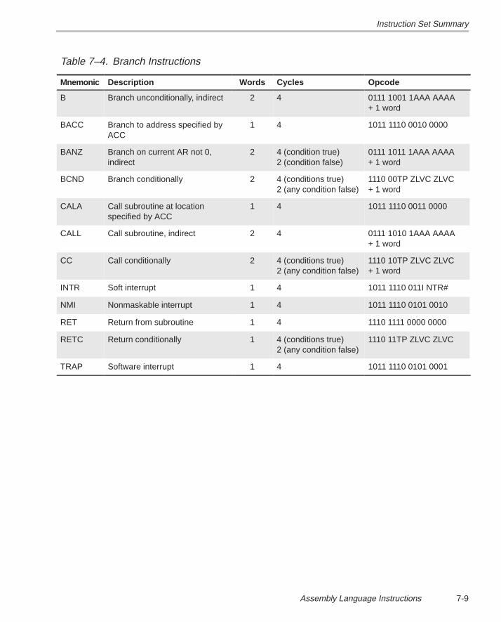
Instruction Set Summary
7-9Assembly Language Instructions
Table 7–4. Branch Instructions
Mnemonic Description Words Cycles Opcode
B Branch unconditionally, indirect 2 4 0111 1001 1AAA AAAA+ 1 word
BACC Branch to address specified byACC
1 4 1011 1110 0010 0000
BANZ Branch on current AR not 0,indirect
2 4 (condition true)2 (condition false)
0111 1011 1AAA AAAA+ 1 word
BCND Branch conditionally 2 4 (conditions true)2 (any condition false)
1110 00TP ZLVC ZLVC+ 1 word
CALA Call subroutine at locationspecified by ACC
1 4 1011 1110 0011 0000
CALL Call subroutine, indirect 2 4 0111 1010 1AAA AAAA+ 1 word
CC Call conditionally 2 4 (conditions true)2 (any condition false)
1110 10TP ZLVC ZLVC+ 1 word
INTR Soft interrupt 1 4 1011 1110 011I NTR#
NMI Nonmaskable interrupt 1 4 1011 1110 0101 0010
RET Return from subroutine 1 4 1110 1111 0000 0000
RETC Return conditionally 1 4 (conditions true)2 (any condition false)
1110 11TP ZLVC ZLVC
TRAP Software interrupt 1 4 1011 1110 0101 0001
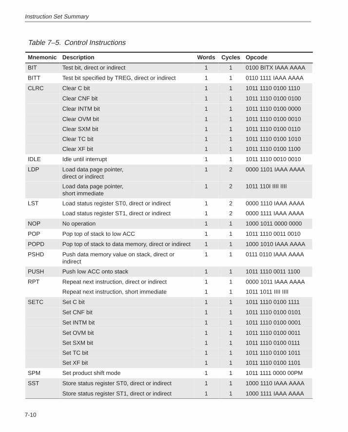
Instruction Set Summary
7-10
Table 7–5. Control Instructions
Mnemonic Description Words Cycles Opcode
BIT Test bit, direct or indirect 1 1 0100 BITX IAAA AAAA
BITT Test bit specified by TREG, direct or indirect 1 1 0110 1111 IAAA AAAA
CLRC Clear C bit 1 1 1011 1110 0100 1110
Clear CNF bit 1 1 1011 1110 0100 0100
Clear INTM bit 1 1 1011 1110 0100 0000
Clear OVM bit 1 1 1011 1110 0100 0010
Clear SXM bit 1 1 1011 1110 0100 0110
Clear TC bit 1 1 1011 1110 0100 1010
Clear XF bit 1 1 1011 1110 0100 1100
IDLE Idle until interrupt 1 1 1011 1110 0010 0010
LDP Load data page pointer,direct or indirect
1 2 0000 1101 IAAA AAAA
Load data page pointer,short immediate
1 2 1011 110I IIII IIII
LST Load status register ST0, direct or indirect 1 2 0000 1110 IAAA AAAA
Load status register ST1, direct or indirect 1 2 0000 1111 IAAA AAAA
NOP No operation 1 1 1000 1011 0000 0000
POP Pop top of stack to low ACC 1 1 1011 1110 0011 0010
POPD Pop top of stack to data memory, direct or indirect 1 1 1000 1010 IAAA AAAA
PSHD Push data memory value on stack, direct orindirect
1 1 0111 0110 IAAA AAAA
PUSH Push low ACC onto stack 1 1 1011 1110 0011 1100
RPT Repeat next instruction, direct or indirect 1 1 0000 1011 IAAA AAAA
Repeat next instruction, short immediate 1 1 1011 1011 IIII IIII
SETC Set C bit 1 1 1011 1110 0100 1111
Set CNF bit 1 1 1011 1110 0100 0101
Set INTM bit 1 1 1011 1110 0100 0001
Set OVM bit 1 1 1011 1110 0100 0011
Set SXM bit 1 1 1011 1110 0100 0111
Set TC bit 1 1 1011 1110 0100 1011
Set XF bit 1 1 1011 1110 0100 1101
SPM Set product shift mode 1 1 1011 1111 0000 00PM
SST Store status register ST0, direct or indirect 1 1 1000 1110 IAAA AAAA
Store status register ST1, direct or indirect 1 1 1000 1111 IAAA AAAA
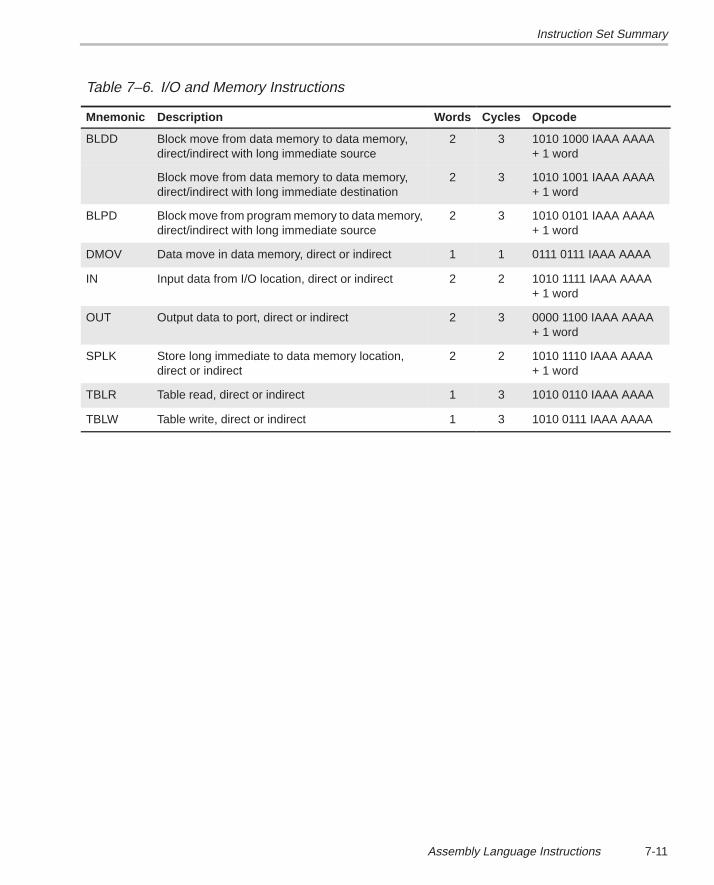
Instruction Set Summary
7-11Assembly Language Instructions
Table 7–6. I/O and Memory Instructions
Mnemonic Description Words Cycles Opcode
BLDD Block move from data memory to data memory,direct/indirect with long immediate source
2 3 1010 1000 IAAA AAAA+ 1 word
Block move from data memory to data memory,direct/indirect with long immediate destination
2 3 1010 1001 IAAA AAAA+ 1 word
BLPD Block move from program memory to data memory,direct/indirect with long immediate source
2 3 1010 0101 IAAA AAAA+ 1 word
DMOV Data move in data memory, direct or indirect 1 1 0111 0111 IAAA AAAA
IN Input data from I/O location, direct or indirect 2 2 1010 1111 IAAA AAAA+ 1 word
OUT Output data to port, direct or indirect 2 3 0000 1100 IAAA AAAA+ 1 word
SPLK Store long immediate to data memory location,direct or indirect
2 2 1010 1110 IAAA AAAA+ 1 word
TBLR Table read, direct or indirect 1 3 1010 0110 IAAA AAAA
TBLW Table write, direct or indirect 1 3 1010 0111 IAAA AAAA
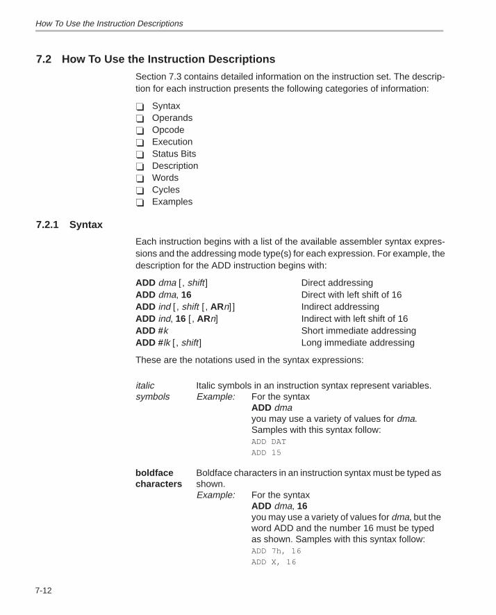
How To Use the Instruction Descriptions
7-12
7.2 How To Use the Instruction Descriptions
Section 7.3 contains detailed information on the instruction set. The descrip-tion for each instruction presents the following categories of information:
Syntax Operands Opcode Execution Status Bits Description Words Cycles Examples
7.2.1 Syntax
Each instruction begins with a list of the available assembler syntax expres-sions and the addressing mode type(s) for each expression. For example, thedescription for the ADD instruction begins with:
ADD dma [ , shift ] Direct addressingADD dma, 16 Direct with left shift of 16ADD ind [ , shift [ , ARn]] Indirect addressingADD ind, 16 [ , ARn] Indirect with left shift of 16ADD #k Short immediate addressingADD #lk [ , shift ] Long immediate addressing
These are the notations used in the syntax expressions:
italicsymbols
Italic symbols in an instruction syntax represent variables.Example: For the syntax
ADD dmayou may use a variety of values for dma.Samples with this syntax follow:ADD DAT
ADD 15
boldfacecharacters
Boldface characters in an instruction syntax must be typed asshown.Example: For the syntax
ADD dma, 16you may use a variety of values for dma, but theword ADD and the number 16 must be typedas shown. Samples with this syntax follow:ADD 7h, 16
ADD X, 16
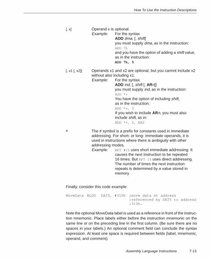
How To Use the Instruction Descriptions
7-13Assembly Language Instructions
[, x] Operand x is optional.Example: For the syntax
ADD dma, [, shift]you must supply dma, as in the instruction:ADD 7h
and you have the option of adding a shift value,as in the instruction:ADD 7h, 5
[, x1 [, x2]] Operands x1 and x2 are optional, but you cannot include x2without also including x1.Example: For the syntax
ADD ind, [, shift [, ARn]]you must supply ind, as in the instruction:ADD *+
You have the option of including shift,as in the instruction:ADD *+, 5
If you wish to include ARn, you must alsoinclude shift, as in:ADD *+, 0, AR2
# The # symbol is a prefix for constants used in immediateaddressing. For short- or long- immediate operands, it isused in instructions where there is ambiguity with otheraddressing modes.Example: RPT #15 uses short immediate addressing. It
causes the next instruction to be repeated16 times. But RPT 15 uses direct addressing.The number of times the next instructionrepeats is determined by a value stored inmemory.
Finally, consider this code example:
MoveData BLDD DAT5, #310h ;move data at address;referenced by DAT5 to address;310h.
Note the optional MoveData label is used as a reference in front of the instruc-tion mnemonic. Place labels either before the instruction mnemonic on thesame line or on the preceding line in the first column. (Be sure there are nospaces in your labels.) An optional comment field can conclude the syntaxexpression. At least one space is required between fields (label, mnemonic,operand, and comment).
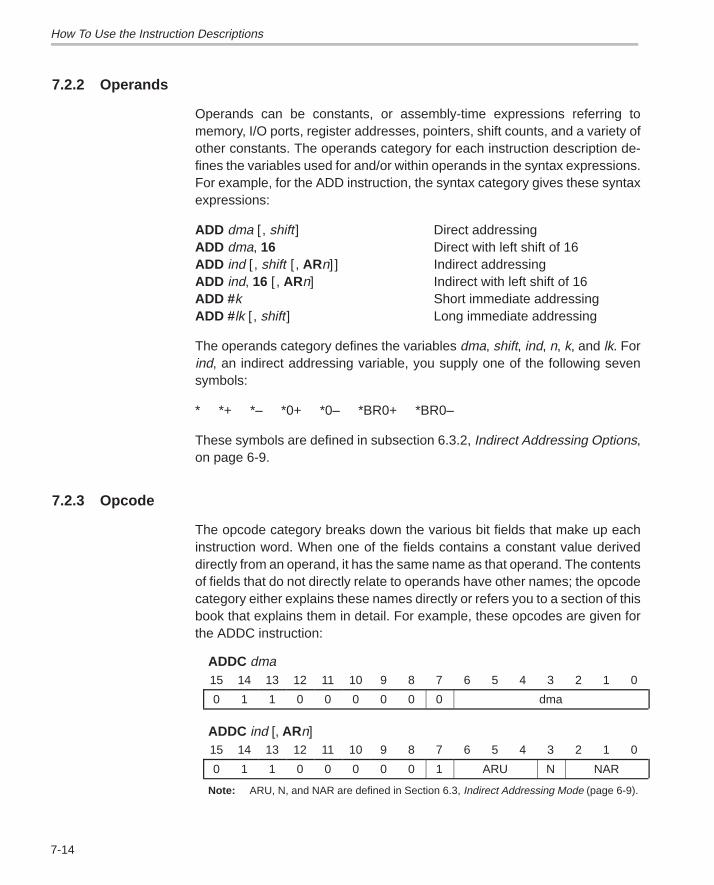
How To Use the Instruction Descriptions
7-14
7.2.2 Operands
Operands can be constants, or assembly-time expressions referring tomemory, I/O ports, register addresses, pointers, shift counts, and a variety ofother constants. The operands category for each instruction description de-fines the variables used for and/or within operands in the syntax expressions.For example, for the ADD instruction, the syntax category gives these syntaxexpressions:
ADD dma [ , shift ] Direct addressingADD dma, 16 Direct with left shift of 16ADD ind [ , shift [ , ARn]] Indirect addressingADD ind, 16 [ , ARn] Indirect with left shift of 16ADD #k Short immediate addressingADD #lk [ , shift ] Long immediate addressing
The operands category defines the variables dma, shift, ind, n, k, and lk. Forind, an indirect addressing variable, you supply one of the following sevensymbols:
* *+ *– *0+ *0– *BR0+ *BR0–
These symbols are defined in subsection 6.3.2, Indirect Addressing Options,on page 6-9.
7.2.3 Opcode
The opcode category breaks down the various bit fields that make up eachinstruction word. When one of the fields contains a constant value deriveddirectly from an operand, it has the same name as that operand. The contentsof fields that do not directly relate to operands have other names; the opcodecategory either explains these names directly or refers you to a section of thisbook that explains them in detail. For example, these opcodes are given forthe ADDC instruction:
ADDC dma15 14 13 12 11 10 9 8 7 6 5 4 3 2 1 0
0 1 1 0 0 0 0 0 0 dma
ADDC ind [,ARn]15 14 13 12 11 10 9 8 7 6 5 4 3 2 1 0
0 1 1 0 0 0 0 0 1 ARU N NAR
Note: ARU, N, and NAR are defined in Section 6.3, Indirect Addressing Mode (page 6-9).
How To Use the Instruction Descriptions
7-15Assembly Language Instructions
The field called dma contains the value dma, which is defined in the operandscategory. The contents of the fields ARU, N, and NAR are derived from the op-erands ind and n but do not directly correspond to those operands; therefore,a note directs you to the appropriate section for more details.
7.2.4 Execution
The execution category presents an instruction operation sequence that de-scribes the processing that takes place when the instruction is executed. If theexecution event or events depend on the addressing mode used, the execu-tion category specifies which events are associated with which addressingmodes. Here are notations used in the execution category:
(r) The content of register or location r.Example: (ACC) represents the value in the accumulator.
x → y Value x is assigned to register or location y.Example: (data-memory address) → ACC means:
The content of the specified data-memoryaddress is put into the accumulator.
r(n:m) Bits n through m of register or location r.Example: ACC(15:0) represents bits 15 through 0 of the
accumulator.
(r(n:m)) The content of bits n through m of register or location r.Example: (ACC(31:16)) represents the content of bits 31
through 16 of the accumulator.
nnh Indicates that nn represents a hexadecimal number.
7.2.5 Status Bits
The bits in status registers ST0 and ST1 affect the operation of certain instruc-tions and are affected by certain instructions. The status bits category of eachinstruction description states which of the bits (if any) affect the execution ofthe instruction and which of the bits (if any) are affected by the instruction.
7.2.6 Description
The description category explains what happens during instruction executionand its effect on the rest of the processor or on memory contents. It also dis-cusses any constraints on the operands imposed by the processor or the as-sembler. This description parallels and supplements the information given inthe execution category.
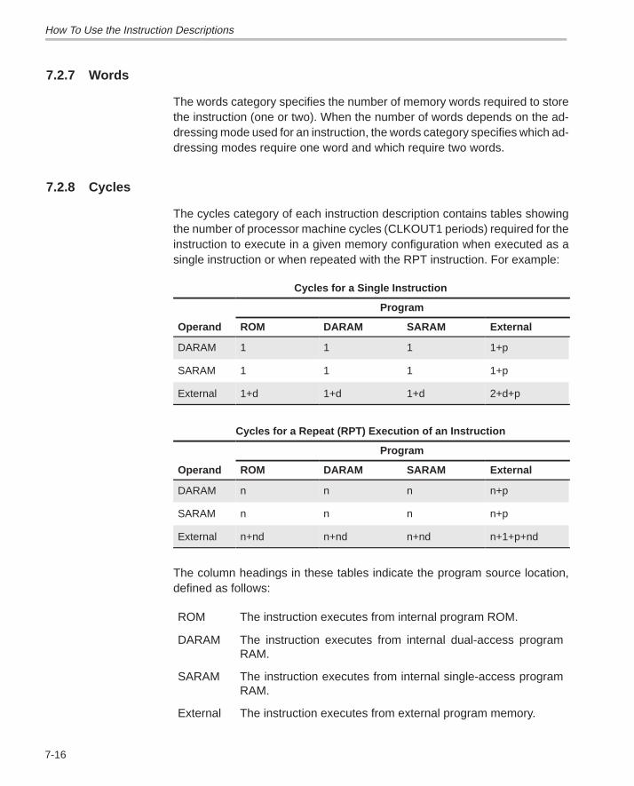
How To Use the Instruction Descriptions
7-16
7.2.7 Words
The words category specifies the number of memory words required to storethe instruction (one or two). When the number of words depends on the ad-dressing mode used for an instruction, the words category specifies which ad-dressing modes require one word and which require two words.
7.2.8 Cycles
The cycles category of each instruction description contains tables showingthe number of processor machine cycles (CLKOUT1 periods) required for theinstruction to execute in a given memory configuration when executed as asingle instruction or when repeated with the RPT instruction. For example:
Cycles for a Single Instruction
Program
Operand ROM DARAM SARAM External
DARAM 1 1 1 1+p
SARAM 1 1 1 1+p
External 1+d 1+d 1+d 2+d+p
Cycles for a Repeat (RPT) Execution of an Instruction
Program
Operand ROM DARAM SARAM External
DARAM n n n n+p
SARAM n n n n+p
External n+nd n+nd n+nd n+1+p+nd
The column headings in these tables indicate the program source location,defined as follows:
ROM The instruction executes from internal program ROM.
DARAM The instruction executes from internal dual-access programRAM.
SARAM The instruction executes from internal single-access programRAM.
External The instruction executes from external program memory.
How To Use the Instruction Descriptions
7-17Assembly Language Instructions
If an instruction requires memory operand(s), the rows in the table indicate thelocation(s) of the operand(s), as defined here:
DARAM The operand is in internal dual-access RAM.
SARAM The operand is in internal single-access RAM.
External The operand is in external memory.
For the RPT mode execution, n indicates the number of times a given instruc-tion is repeated by an RPT instruction. Additional cycles (wait states) can begenerated for program-memory, data-memory, and I/O accesses by the wait-state generator or by the external READY signal. These additional wait statesare represented in the tables by the following variables:
p Program-memory wait states. Represents the number of addition-al clock cycles the device waits for external program memory torespond to a single access.
d Data-memory wait states. Represents the number of additionalclock cycles the device waits for external data memory to respondto a single access.
io I/O wait states. Represents the number of additional clock cyclesthe device waits for an external I/O device to respond to a singleaccess.
n Number of repetitions (where n > 2 to fill the pipeline). Representsthe number of times a repeated instruction is executed.
If there are multiple accesses to one of the spaces, the variable is precededby the appropriate integer multiple. For example, two accesses to external pro-gram memory would require 2p wait states. The above variables may also usethe subscripts src, dst, and code to indicate source, destination, and code,respectively.
The internal single-access memory on each ’C240 processor is divided into2K-word blocks contiguous in address space. All ’C240 processors supportparallel accesses to these internal single-access RAM blocks. Furthermore,one single access block allows only one access per cycle. Thus, the processorcan read/write on single-access RAM block while accessing another single-access RAM block at the same time.
How To Use the Instruction Descriptions
7-18
All external reads take at least one machine cycle while all external writes takeat least two machine cycles. However, if an external write is immediately fol-lowed or preceded by an external read cycle, then the external write requiresthree cycles. If the wait state generator or the READY pin is used to add m(m > 0) wait states to an external access, then external reads require m + 1cycles, and external write accesses require m + 2 cycles.
The instruction-cycle timings are based on the following assumptions:
At least the next four instructions are fetched from the same memory sec-tion (internal or external) that was used to fetch the current instruction (ex-cept in the case of PC discontinuity instructions, such as B, CALL, etc.)
In the single-execution mode, there is no pipeline conflict between the cur-rent instruction and the instructions immediately preceding or followingthat instruction. The only exception is the conflict between the fetch phaseof the pipeline and the memory read/write (if any) access of the instructionunder consideration. See Section 5.2, Pipeline Operation, on page 5-7 formore information about pipeline operations.
In the repeat execution mode, all conflicts caused by the pipelined execu-tion of an instruction are considered.
7.2.9 Examples
Example code is included for each instruction. The effect of the code onmemory and/or registers is summarized. Consider this example of the ADDinstruction:
ADD*+,0,AR0Before Instruction After Instruction
ARP 4 ARP 0
AR4 0302h AR4 0303h
Data Memory Data Memory302h 2h 302h 2h
ACC X 2h ACC 0 04h
C C
Here are the facts and events represented in this example:
The auxiliary register pointer (ARP) points to the current auxiliary register.Because ARP = 4, the current auxiliary register is AR4.
When the addition takes place, the CPU follows AR4 to data-memoryaddress 0302h. The content of that address, 2h, is added to the contentof the accumulator, also 2h. The result (4h) is placed in the accumulator.(Because the second operand of the instruction specifies a left shift of 0,the data-memory value is not shifted before being added to the accumula-tor value.)
Instruction Descriptions
7-19Assembly Language Instructions
The instruction specifies an increment of 1 for the contents of the currentauxiliary register (*+); therefore, after the addition is performed, the con-tent of AR4 is incremented to 0303h.
The instruction also specifies that AR0 is the next auxiliary register; there-fore, after the instruction ARP = 0.
Because no carry is generated during the addition, the carry bit (C) iscleared to 0.
7.3 Instruction Descriptions
This section contains detailed information on the instruction set for the ’C240.A summary of the instruction set is shown in Section 7.1 on page 7-2. Theinstructions are presented alphabetically, and the description for each instruc-tion presents the following categories of information:
Syntax Operands Opcode Execution Status Bits Description Words Cycles Examples
For a description of how to use each of these categories, see Section 7.2 onpage 7-12.
How To Use the Instruction Descriptions / Instruction Descriptions
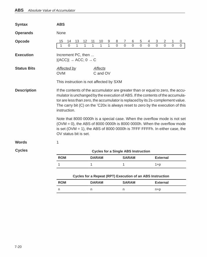
ABS Absolute Value of Accumulator
7-20
Syntax ABS
Operands None
Opcode 01234567891011121314150000000001111101
Execution Increment PC, then ...|(ACC)| → ACC; 0 → C
Status Bits Affected by AffectsOVM C and OV
This instruction is not affected by SXM
Description If the contents of the accumulator are greater than or equal to zero, the accu-mulator is unchanged by the execution of ABS. If the contents of the accumula-tor are less than zero, the accumulator is replaced by its 2s-complement value.The carry bit (C) on the ’C20x is always reset to zero by the execution of thisinstruction.
Note that 8000 0000h is a special case. When the overflow mode is not set(OVM = 0), the ABS of 8000 0000h is 8000 0000h. When the overflow modeis set (OVM = 1), the ABS of 8000 0000h is 7FFF FFFFh. In either case, theOV status bit is set.
Words 1
Cycles for a Single ABS Instruction
ROM DARAM SARAM External
1 1 1 1+p
Cycles for a Repeat (RPT) Execution of an ABS Instruction
ROM DARAM SARAM External
n n n n+p
Cycles
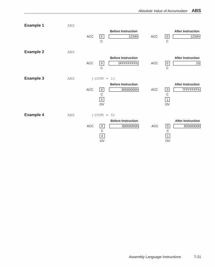
Absolute Value of Accumulator ABS
7-21 Assembly Language Instructions
Example 1 ABS
Before Instruction After Instruction
ACC X 1234h ACC 0 1234h
C C
Example 2 ABS
Before Instruction After Instruction
ACC X 0FFFFFFFFh ACC 0 1h
C C
Example 3 ABS ;(OVM = 1)
Before Instruction After Instruction
ACC X 80000000h ACC 0 7FFFFFFFh
C C
X 1
OV OV
Example 4 ABS ;(OVM = 0)
Before Instruction After Instruction
ACC X 80000000h ACC 0 80000000h
C C
X 1
OV OV
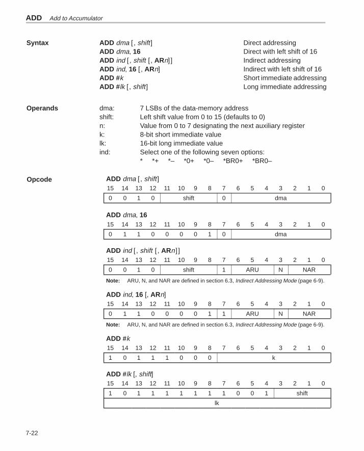
ADD Add to Accumulator
7-22
Syntax ADD dma [ , shift ] Direct addressingADD dma, 16 Direct with left shift of 16ADD ind [ , shift [ , ARn]] Indirect addressingADD ind, 16 [ , ARn] Indirect with left shift of 16ADD #k Short immediate addressingADD #lk [ , shift ] Long immediate addressing
Operands dma: 7 LSBs of the data-memory addressshift: Left shift value from 0 to 15 (defaults to 0)n: Value from 0 to 7 designating the next auxiliary registerk: 8-bit short immediate valuelk: 16-bit long immediate valueind: Select one of the following seven options:
* *+ *– *0+ *0– *BR0+ *BR0–
ADD dma [ , shift ]15 14 13 12 11 10 9 8 7 6 5 4 3 2 1 0
0 0 1 0 shift 0 dma
ADD dma, 1615 14 13 12 11 10 9 8 7 6 5 4 3 2 1 0
0 1 1 0 0 0 0 1 0 dma
ADD ind [, shift [, ARn]]15 14 13 12 11 10 9 8 7 6 5 4 3 2 1 0
0 0 1 0 shift 1 ARU N NAR
Note: ARU, N, and NAR are defined in section 6.3, Indirect Addressing Mode (page 6-9).
ADD ind, 16 [, ARn]15 14 13 12 11 10 9 8 7 6 5 4 3 2 1 0
0 1 1 0 0 0 0 1 1 ARU N NAR
Note: ARU, N, and NAR are defined in section 6.3, Indirect Addressing Mode (page 6-9).
ADD #k15 14 13 12 11 10 9 8 7 6 5 4 3 2 1 0
1 0 1 1 1 0 0 0 k
ADD #lk [, shift]15 14 13 12 11 10 9 8 7 6 5 4 3 2 1 0
1 0 1 1 1 1 1 1 1 0 0 1 shift
lk
Opcode
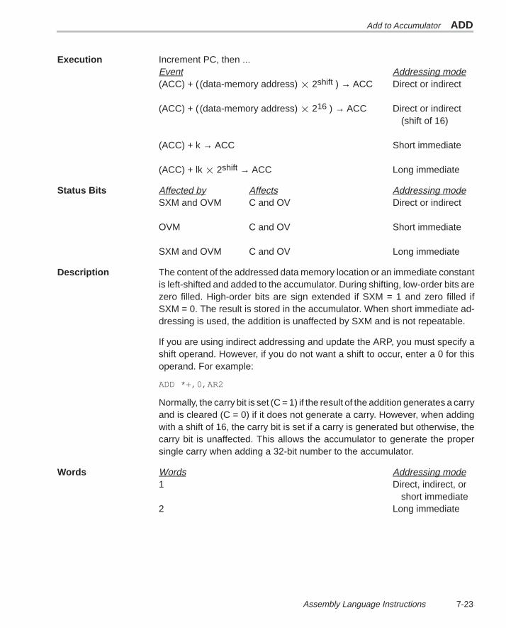
Add to Accumulator ADD
7-23 Assembly Language Instructions
Execution Increment PC, then ...Event Addressing mode(ACC) + ((data-memory address) 2shift ) → ACC Direct or indirect
(ACC) + ((data-memory address) 216 ) → ACC Direct or indirect(shift of 16)
(ACC) + k → ACC Short immediate
(ACC) + lk 2shift → ACC Long immediate
Status Bits Affected by Affects Addressing modeSXM and OVM C and OV Direct or indirect
OVM C and OV Short immediate
SXM and OVM C and OV Long immediate
Description The content of the addressed data memory location or an immediate constantis left-shifted and added to the accumulator. During shifting, low-order bits arezero filled. High-order bits are sign extended if SXM = 1 and zero filled ifSXM = 0. The result is stored in the accumulator. When short immediate ad-dressing is used, the addition is unaffected by SXM and is not repeatable.
If you are using indirect addressing and update the ARP, you must specify ashift operand. However, if you do not want a shift to occur, enter a 0 for thisoperand. For example:
ADD *+,0,AR2
Normally, the carry bit is set (C = 1) if the result of the addition generates a carryand is cleared (C = 0) if it does not generate a carry. However, when addingwith a shift of 16, the carry bit is set if a carry is generated but otherwise, thecarry bit is unaffected. This allows the accumulator to generate the propersingle carry when adding a 32-bit number to the accumulator.
Words Words Addressing mode1 Direct, indirect, or
short immediate2 Long immediate
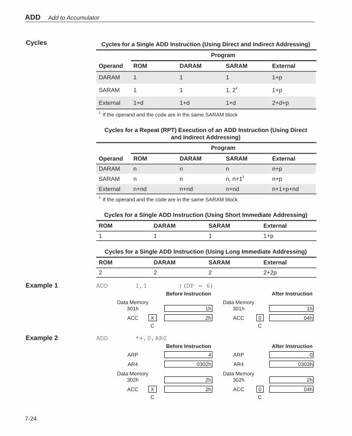
ADD Add to Accumulator
7-24
Cycles for a Single ADD Instruction (Using Direct and Indirect Addressing)
Program
Operand ROM DARAM SARAM External
DARAM 1 1 1 1+p
SARAM 1 1 1, 2† 1+p
External 1+d 1+d 1+d 2+d+p
† If the operand and the code are in the same SARAM block
Cycles for a Repeat (RPT) Execution of an ADD Instruction (Using Directand Indirect Addressing)
Program
Operand ROM DARAM SARAM External
DARAM n n n n+p
SARAM n n n, n+1† n+p
External n+nd n+nd n+nd n+1+p+nd
† If the operand and the code are in the same SARAM block
Cycles for a Single ADD Instruction (Using Short Immediate Addressing)
ROM DARAM SARAM External
1 1 1 1+p
Cycles for a Single ADD Instruction (Using Long Immediate Addressing)
ROM DARAM SARAM External
2 2 2 2+2p
Example 1 ADD 1,1 ;(DP = 6)Before Instruction After Instruction
Data Memory Data Memory301h 1h 301h 1h
ACC X 2h ACC 0 04h
C C
Example 2 ADD *+,0,AR0Before Instruction After Instruction
ARP 4 ARP 0
AR4 0302h AR4 0303h
Data Memory Data Memory302h 2h 302h 2h
ACC X 2h ACC 0 04h
C C
Cycles
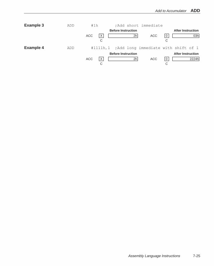
Add to Accumulator ADD
7-25 Assembly Language Instructions
Example 3 ADD #1h ;Add short immediateBefore Instruction After Instruction
ACC X 2h ACC 0 03h
C C
Example 4 ADD #1111h,1 ;Add long immediate with shift of 1
Before Instruction After Instruction
ACC X 2h ACC 0 2224h
C C
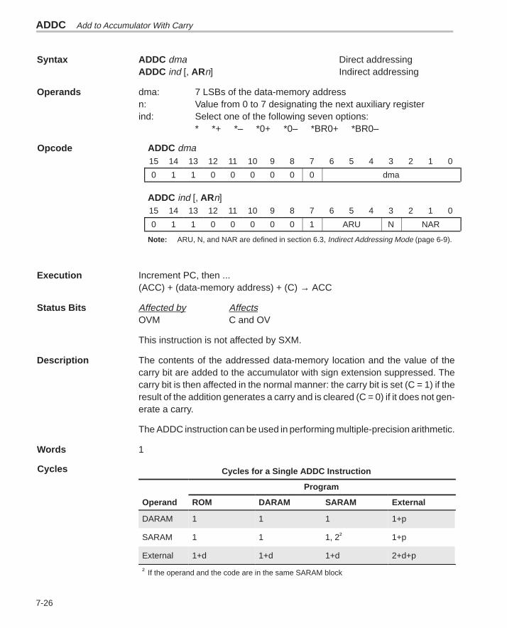
ADDC Add to Accumulator With Carry
7-26
Syntax ADDC dma Direct addressingADDC ind [, ARn] Indirect addressing
Operands dma: 7 LSBs of the data-memory addressn: Value from 0 to 7 designating the next auxiliary registerind: Select one of the following seven options:
* *+ *– *0+ *0– *BR0+ *BR0–
ADDC dma15 14 13 12 11 10 9 8 7 6 5 4 3 2 1 0
0 1 1 0 0 0 0 0 0 dma
ADDC ind [,ARn]15 14 13 12 11 10 9 8 7 6 5 4 3 2 1 0
0 1 1 0 0 0 0 0 1 ARU N NAR
Note: ARU, N, and NAR are defined in section 6.3, Indirect Addressing Mode (page 6-9).
Execution Increment PC, then ...(ACC) + (data-memory address) + (C) → ACC
Status Bits Affected by AffectsOVM C and OV
This instruction is not affected by SXM.
Description The contents of the addressed data-memory location and the value of thecarry bit are added to the accumulator with sign extension suppressed. Thecarry bit is then affected in the normal manner: the carry bit is set (C = 1) if theresult of the addition generates a carry and is cleared (C = 0) if it does not gen-erate a carry.
The ADDC instruction can be used in performing multiple-precision arithmetic.
Words 1
Cycles for a Single ADDC Instruction
Program
Operand ROM DARAM SARAM External
DARAM 1 1 1 1+p
SARAM 1 1 1, 2† 1+p
External 1+d 1+d 1+d 2+d+p
† If the operand and the code are in the same SARAM block
Opcode
Cycles
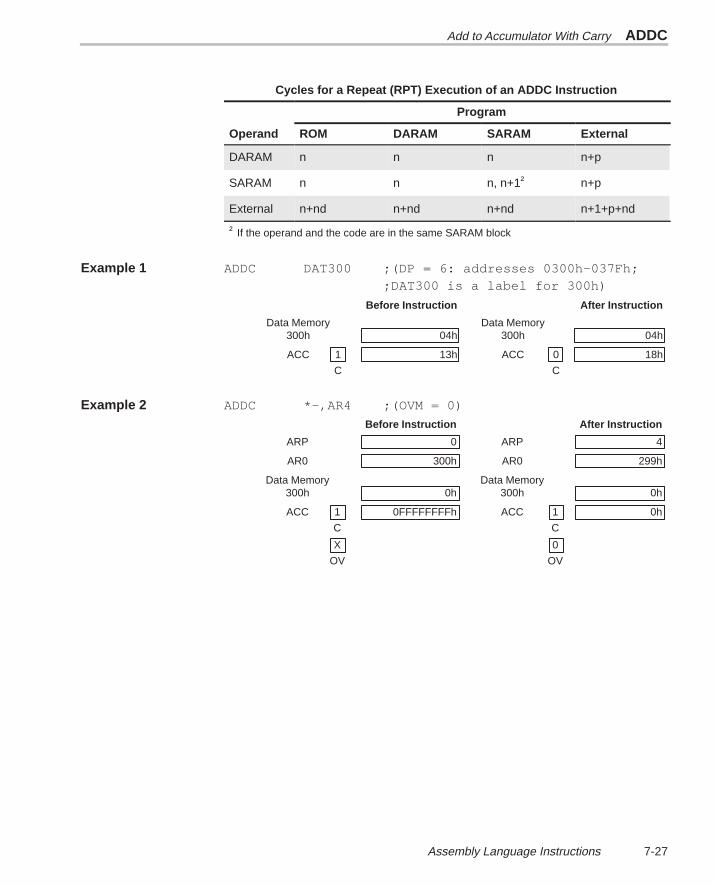
Add to Accumulator With Carry ADDC
7-27 Assembly Language Instructions
Cycles for a Repeat (RPT) Execution of an ADDC Instruction
Program
Operand ROM DARAM SARAM External
DARAM n n n n+p
SARAM n n n, n+1† n+p
External n+nd n+nd n+nd n+1+p+nd
† If the operand and the code are in the same SARAM block
Example 1 ADDC DAT300 ;(DP = 6: addresses 0300h–037Fh;;DAT300 is a label for 300h)
Before Instruction After Instruction
Data Memory Data Memory300h 04h 300h 04h
ACC 1 13h ACC 0 18h
C C
Example 2 ADDC *–,AR4 ;(OVM = 0)
Before Instruction After Instruction
ARP 0 ARP 4
AR0 300h AR0 299h
Data Memory Data Memory300h 0h 300h 0h
ACC 1 0FFFFFFFFh ACC 1 0h
C C
X 0
OV OV
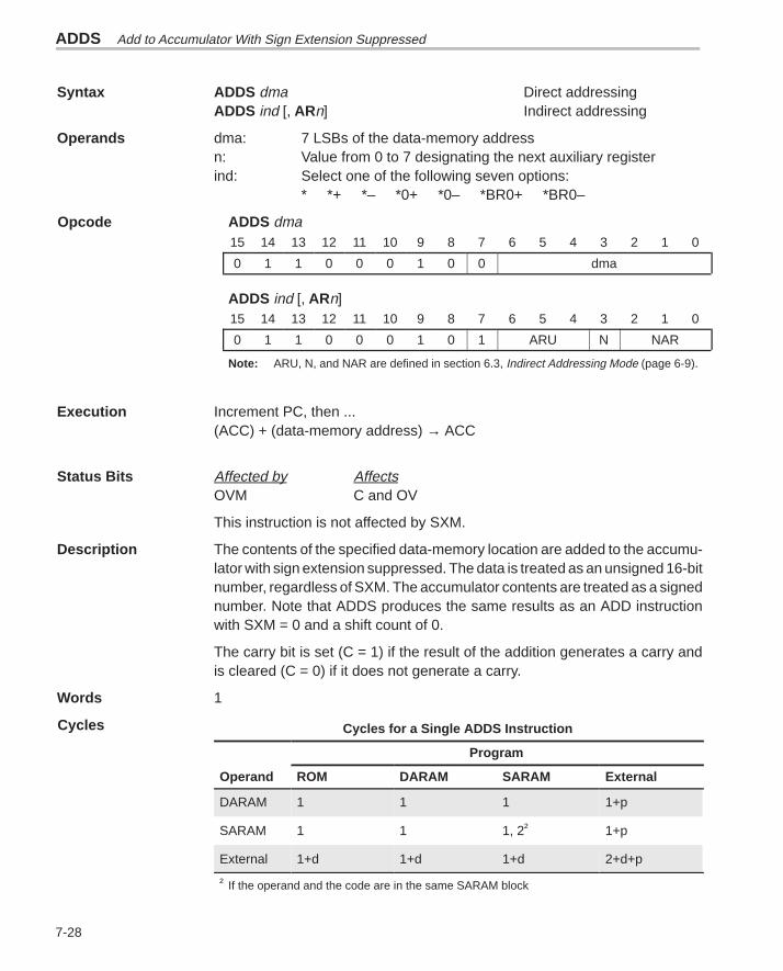
ADDS Add to Accumulator With Sign Extension Suppressed
7-28
Syntax ADDS dma Direct addressingADDS ind [,ARn] Indirect addressing
Operands dma: 7 LSBs of the data-memory addressn: Value from 0 to 7 designating the next auxiliary registerind: Select one of the following seven options:
* *+ *– *0+ *0– *BR0+ *BR0–
ADDS dma15 14 13 12 11 10 9 8 7 6 5 4 3 2 1 0
0 1 1 0 0 0 1 0 0 dma
ADDS ind [,ARn]15 14 13 12 11 10 9 8 7 6 5 4 3 2 1 0
0 1 1 0 0 0 1 0 1 ARU N NAR
Note: ARU, N, and NAR are defined in section 6.3, Indirect Addressing Mode (page 6-9).
Execution Increment PC, then ...(ACC) + (data-memory address) → ACC
Status Bits Affected by AffectsOVM C and OV
This instruction is not affected by SXM.
Description The contents of the specified data-memory location are added to the accumu-lator with sign extension suppressed. The data is treated as an unsigned 16-bitnumber, regardless of SXM. The accumulator contents are treated as a signednumber. Note that ADDS produces the same results as an ADD instructionwith SXM = 0 and a shift count of 0.
The carry bit is set (C = 1) if the result of the addition generates a carry andis cleared (C = 0) if it does not generate a carry.
Words 1
Cycles for a Single ADDS Instruction
Program
Operand ROM DARAM SARAM External
DARAM 1 1 1 1+p
SARAM 1 1 1, 2† 1+p
External 1+d 1+d 1+d 2+d+p
† If the operand and the code are in the same SARAM block
Opcode
Cycles
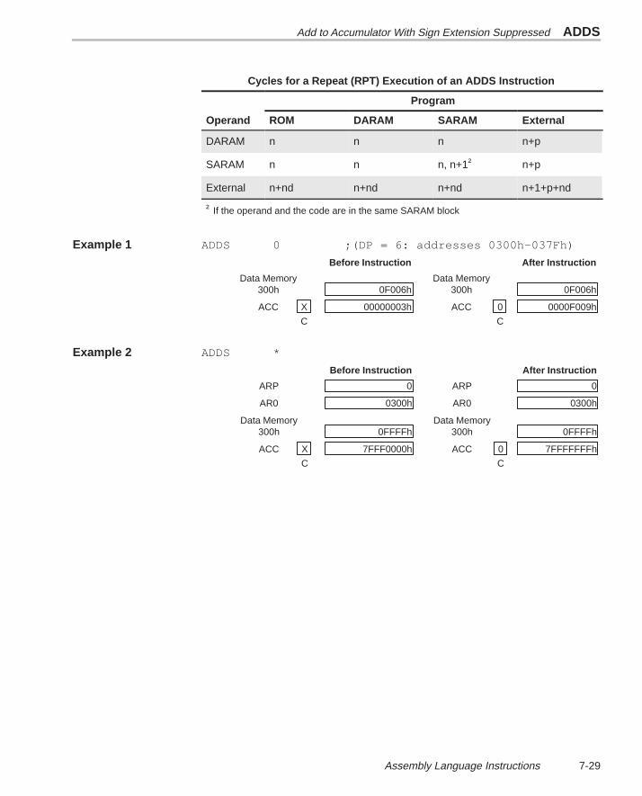
Add to Accumulator With Sign Extension Suppressed ADDS
7-29 Assembly Language Instructions
Cycles for a Repeat (RPT) Execution of an ADDS Instruction
Program
Operand ROM DARAM SARAM External
DARAM n n n n+p
SARAM n n n, n+1† n+p
External n+nd n+nd n+nd n+1+p+nd
† If the operand and the code are in the same SARAM block
Example 1 ADDS 0 ;(DP = 6: addresses 0300h–037Fh)
Before Instruction After Instruction
Data Memory Data Memory300h 0F006h 300h 0F006h
ACC X 00000003h ACC 0 0000F009h
C C
Example 2 ADDS *
Before Instruction After Instruction
ARP 0 ARP 0
AR0 0300h AR0 0300h
Data Memory Data Memory300h 0FFFFh 300h 0FFFFh
ACC X 7FFF0000h ACC 0 7FFFFFFFh
C C
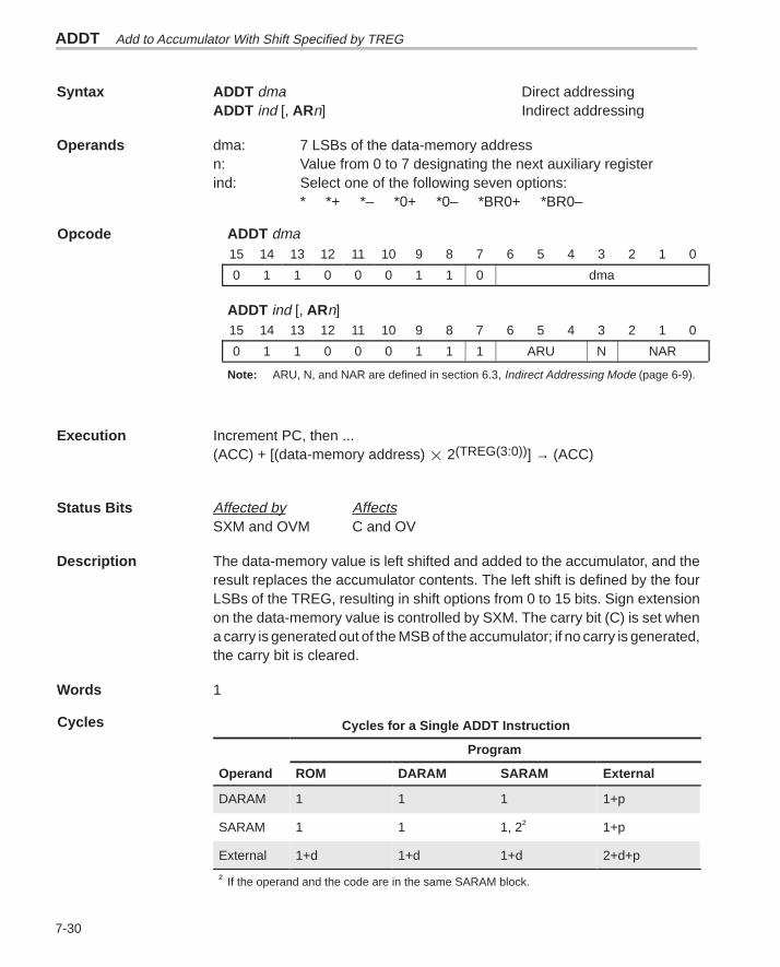
ADDT Add to Accumulator With Shift Specified by TREG
7-30
Syntax ADDT dma Direct addressingADDT ind [,ARn] Indirect addressing
Operands dma: 7 LSBs of the data-memory addressn: Value from 0 to 7 designating the next auxiliary registerind: Select one of the following seven options:
* *+ *– *0+ *0– *BR0+ *BR0–
ADDT dma15 14 13 12 11 10 9 8 7 6 5 4 3 2 1 0
0 1 1 0 0 0 1 1 0 dma
ADDT ind [, ARn]15 14 13 12 11 10 9 8 7 6 5 4 3 2 1 0
0 1 1 0 0 0 1 1 1 ARU N NAR
Note: ARU, N, and NAR are defined in section 6.3, Indirect Addressing Mode (page 6-9).
Execution Increment PC, then ...(ACC) + [(data-memory address) 2(TREG(3:0))] → (ACC)
Status Bits Affected by AffectsSXM and OVM C and OV
Description The data-memory value is left shifted and added to the accumulator, and theresult replaces the accumulator contents. The left shift is defined by the fourLSBs of the TREG, resulting in shift options from 0 to 15 bits. Sign extensionon the data-memory value is controlled by SXM. The carry bit (C) is set whena carry is generated out of the MSB of the accumulator; if no carry is generated,the carry bit is cleared.
Words 1
Cycles for a Single ADDT Instruction
Program
Operand ROM DARAM SARAM External
DARAM 1 1 1 1+p
SARAM 1 1 1, 2† 1+p
External 1+d 1+d 1+d 2+d+p
† If the operand and the code are in the same SARAM block.
Opcode
Cycles
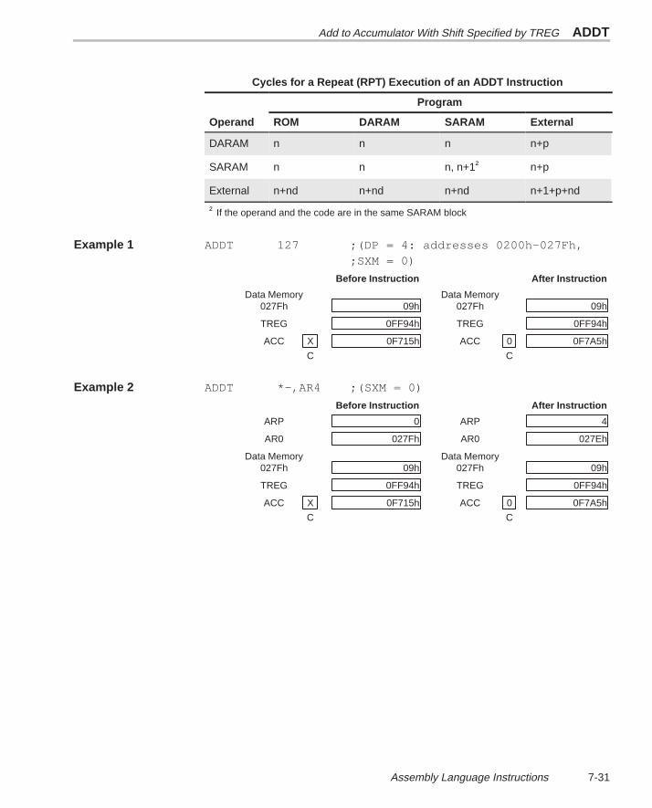
Add to Accumulator With Shift Specified by TREG ADDT
7-31 Assembly Language Instructions
Cycles for a Repeat (RPT) Execution of an ADDT Instruction
Program
Operand ROM DARAM SARAM External
DARAM n n n n+p
SARAM n n n, n+1† n+p
External n+nd n+nd n+nd n+1+p+nd
† If the operand and the code are in the same SARAM block
Example 1 ADDT 127 ;(DP = 4: addresses 0200h–027Fh,;SXM = 0)
Before Instruction After Instruction
Data Memory Data Memory027Fh 09h 027Fh 09h
TREG 0FF94h TREG 0FF94h
ACC X 0F715h ACC 0 0F7A5h
C C
Example 2 ADDT *–,AR4 ;(SXM = 0)
Before Instruction After Instruction
ARP 0 ARP 4
AR0 027Fh AR0 027Eh
Data Memory Data Memory027Fh 09h 027Fh 09h
TREG 0FF94h TREG 0FF94h
ACC X 0F715h ACC 0 0F7A5h
C C
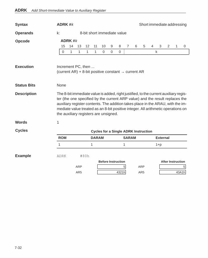
ADRK Add Short-Immediate Value to Auxiliary Register
7-32
Syntax ADRK #k Short immediate addressing
Operands k: 8-bit short immediate value
ADRK #k15 14 13 12 11 10 9 8 7 6 5 4 3 2 1 0
0 1 1 1 1 0 0 0 k
Execution Increment PC, then ...(current AR) + 8-bit positive constant → current AR
Status Bits None
Description The 8-bit immediate value is added, right justified, to the current auxiliary regis-ter (the one specified by the current ARP value) and the result replaces theauxiliary register contents. The addition takes place in the ARAU, with the im-mediate value treated as an 8-bit positive integer. All arithmetic operations onthe auxiliary registers are unsigned.
Words 1
Cycles for a Single ADRK Instruction
ROM DARAM SARAM External
1 1 1 1+p
Example ADRK #80h
Before Instruction After Instruction
ARP 5 ARP 5
AR5 4321h AR5 43A1h
Opcode
Cycles
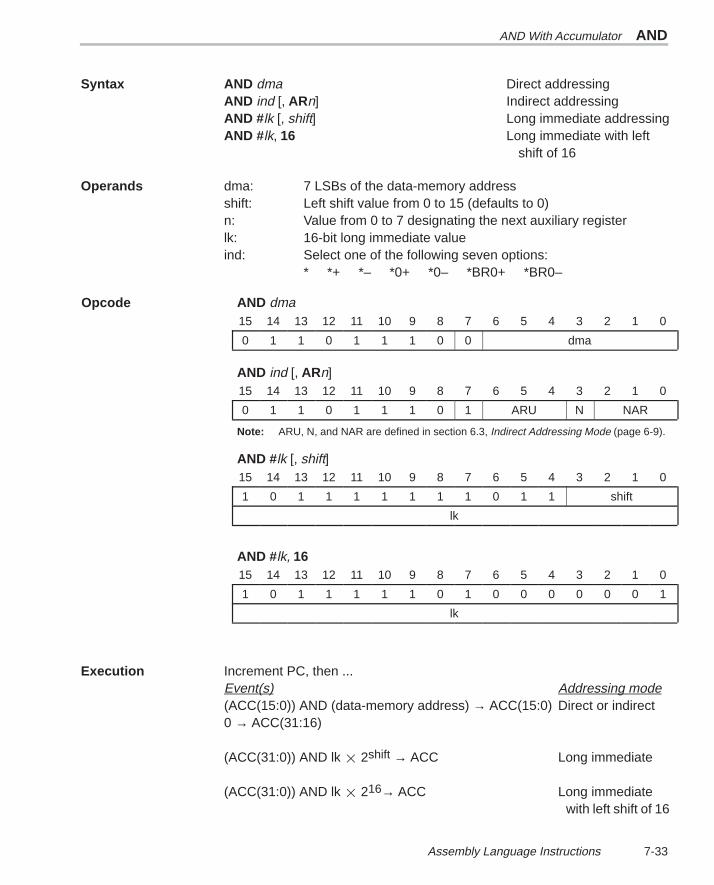
AND With Accumulator AND
7-33 Assembly Language Instructions
Syntax AND dma Direct addressingAND ind [,ARn] Indirect addressingAND #lk [,shift] Long immediate addressingAND #lk,16 Long immediate with left
shift of 16
Operands dma: 7 LSBs of the data-memory addressshift: Left shift value from 0 to 15 (defaults to 0)n: Value from 0 to 7 designating the next auxiliary registerlk: 16-bit long immediate valueind: Select one of the following seven options:
* *+ *– *0+ *0– *BR0+ *BR0–
AND dma15 14 13 12 11 10 9 8 7 6 5 4 3 2 1 0
0 1 1 0 1 1 1 0 0 dma
AND ind [,ARn]15 14 13 12 11 10 9 8 7 6 5 4 3 2 1 0
0 1 1 0 1 1 1 0 1 ARU N NAR
Note: ARU, N, and NAR are defined in section 6.3, Indirect Addressing Mode (page 6-9).
AND #lk [,shift]15 14 13 12 11 10 9 8 7 6 5 4 3 2 1 0
1 0 1 1 1 1 1 1 1 0 1 1 shift
lk
AND #lk,1615 14 13 12 11 10 9 8 7 6 5 4 3 2 1 0
1 0 1 1 1 1 1 0 1 0 0 0 0 0 0 1
lk
Execution Increment PC, then ...Event(s) Addressing mode(ACC(15:0)) AND (data-memory address) → ACC(15:0) Direct or indirect0 → ACC(31:16)
(ACC(31:0)) AND lk 2shift → ACC Long immediate
(ACC(31:0)) AND lk 216→ ACC Long immediatewith left shift of 16
Opcode
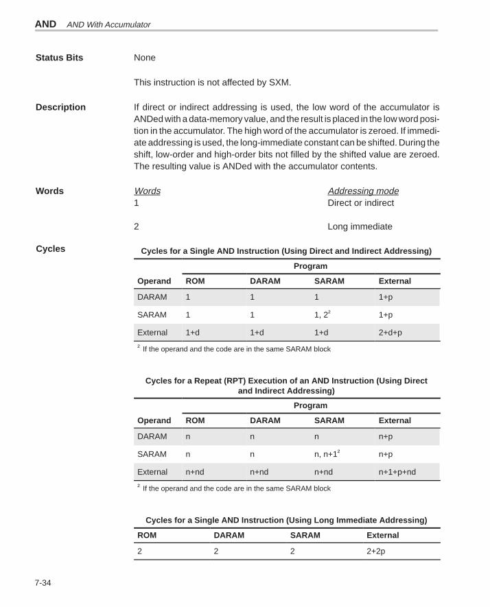
AND AND With Accumulator
7-34
Status Bits None
This instruction is not affected by SXM.
Description If direct or indirect addressing is used, the low word of the accumulator isANDed with a data-memory value, and the result is placed in the low word posi-tion in the accumulator. The high word of the accumulator is zeroed. If immedi-ate addressing is used, the long-immediate constant can be shifted. During theshift, low-order and high-order bits not filled by the shifted value are zeroed.The resulting value is ANDed with the accumulator contents.
Words Words Addressing mode1 Direct or indirect
2 Long immediate
Cycles for a Single AND Instruction (Using Direct and Indirect Addressing)
Program
Operand ROM DARAM SARAM External
DARAM 1 1 1 1+p
SARAM 1 1 1, 2† 1+p
External 1+d 1+d 1+d 2+d+p
† If the operand and the code are in the same SARAM block
Cycles for a Repeat (RPT) Execution of an AND Instruction (Using Directand Indirect Addressing)
Program
Operand ROM DARAM SARAM External
DARAM n n n n+p
SARAM n n n, n+1† n+p
External n+nd n+nd n+nd n+1+p+nd
† If the operand and the code are in the same SARAM block
Cycles for a Single AND Instruction (Using Long Immediate Addressing)
ROM DARAM SARAM External
2 2 2 2+2p
Cycles
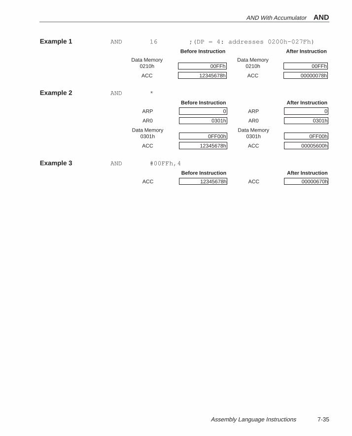
AND With Accumulator AND
7-35 Assembly Language Instructions
Example 1 AND 16 ;(DP = 4: addresses 0200h–027Fh)
Before Instruction After Instruction
Data Memory Data Memory0210h 00FFh 0210h 00FFh
ACC 12345678h ACC 00000078h
Example 2 AND *
Before Instruction After Instruction
ARP 0 ARP 0
AR0 0301h AR0 0301h
Data Memory Data Memory0301h 0FF00h 0301h 0FF00h
ACC 12345678h ACC 00005600h
Example 3 AND #00FFh,4
Before Instruction After Instruction
ACC 12345678h ACC 00000670h
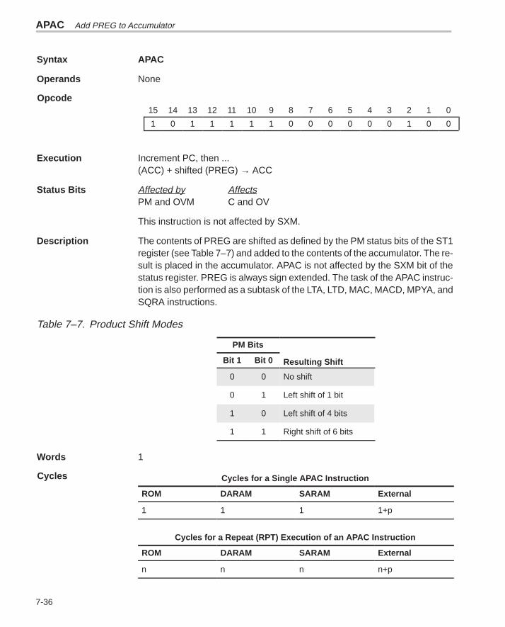
APAC Add PREG to Accumulator
7-36
Syntax APAC
Operands None
15 14 13 12 11 10 9 8 7 6 5 4 3 2 1 0
1 0 1 1 1 1 1 0 0 0 0 0 0 1 0 0
Execution Increment PC, then ...(ACC) + shifted (PREG) → ACC
Status Bits Affected by AffectsPM and OVM C and OV
This instruction is not affected by SXM.
Description The contents of PREG are shifted as defined by the PM status bits of the ST1register (see Table 7–7) and added to the contents of the accumulator. The re-sult is placed in the accumulator. APAC is not affected by the SXM bit of thestatus register. PREG is always sign extended. The task of the APAC instruc-tion is also performed as a subtask of the LTA, LTD, MAC, MACD, MPYA, andSQRA instructions.
Table 7–7. Product Shift Modes
PM Bits
Bit 1 Bit 0 Resulting Shift
0 0 No shift
0 1 Left shift of 1 bit
1 0 Left shift of 4 bits
1 1 Right shift of 6 bits
Words 1
Cycles for a Single APAC Instruction
ROM DARAM SARAM External
1 1 1 1+p
Cycles for a Repeat (RPT) Execution of an APAC Instruction
ROM DARAM SARAM External
n n n n+p
Opcode
Cycles
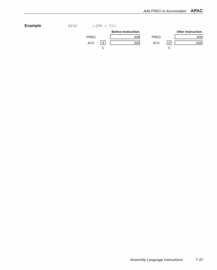
Add PREG to Accumulator APAC
7-37 Assembly Language Instructions
Example APAC ;(PM = 01)
Before Instruction After Instruction
PREG 40h PREG 40h
ACC X 20h ACC 0 A0h
C C
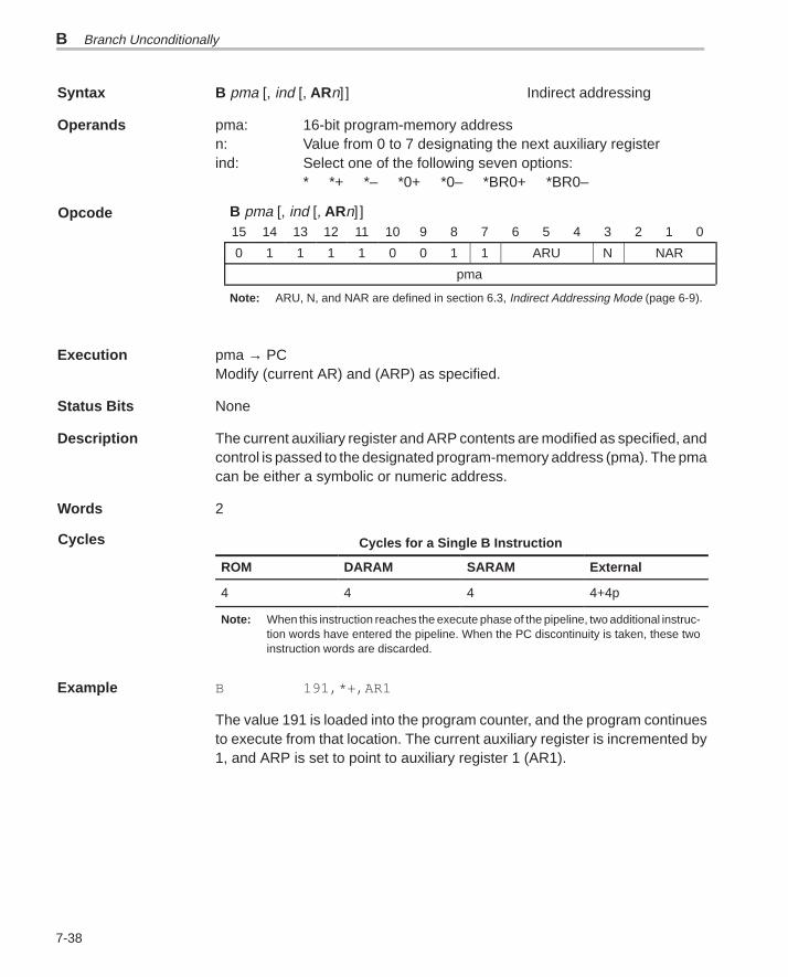
B Branch Unconditionally
7-38
Syntax B pma [, ind [,ARn]] Indirect addressing
Operands pma: 16-bit program-memory addressn: Value from 0 to 7 designating the next auxiliary registerind: Select one of the following seven options:
* *+ *– *0+ *0– *BR0+ *BR0–
B pma [, ind [,ARn]]15 14 13 12 11 10 9 8 7 6 5 4 3 2 1 0
0 1 1 1 1 0 0 1 1 ARU N NAR
pma
Note: ARU, N, and NAR are defined in section 6.3, Indirect Addressing Mode (page 6-9).
Execution pma → PCModify (current AR) and (ARP) as specified.
Status Bits None
Description The current auxiliary register and ARP contents are modified as specified, andcontrol is passed to the designated program-memory address (pma). The pmacan be either a symbolic or numeric address.
Words 2
Cycles for a Single B Instruction
ROM DARAM SARAM External
4 4 4 4+4p
Note: When this instruction reaches the execute phase of the pipeline, two additional instruc-tion words have entered the pipeline. When the PC discontinuity is taken, these twoinstruction words are discarded.
Example B 191,*+,AR1
The value 191 is loaded into the program counter, and the program continuesto execute from that location. The current auxiliary register is incremented by1, and ARP is set to point to auxiliary register 1 (AR1).
Opcode
Cycles
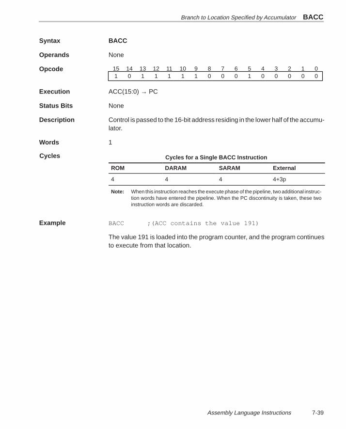
Branch to Location Specified by Accumulator BACC
7-39 Assembly Language Instructions
Syntax BACC
Operands None
Opcode 01234567891011121314150000010001111101
Execution ACC(15:0) → PC
Status Bits None
Description Control is passed to the 16-bit address residing in the lower half of the accumu-lator.
Words 1
Cycles for a Single BACC Instruction
ROM DARAM SARAM External
4 4 4 4+3p
Note: When this instruction reaches the execute phase of the pipeline, two additional instruc-tion words have entered the pipeline. When the PC discontinuity is taken, these twoinstruction words are discarded.
Example BACC ;(ACC contains the value 191)
The value 191 is loaded into the program counter, and the program continuesto execute from that location.
Cycles
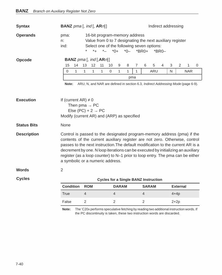
BANZ Branch on Auxiliary Register Not Zero
7-40
Syntax BANZ pma [, ind [, ARn]] Indirect addressing
Operands pma: 16-bit program-memory addressn: Value from 0 to 7 designating the next auxiliary registerind: Select one of the following seven options:
* *+ *– *0+ *0– *BR0+ *BR0–
BANZ pma [, ind [,ARn]]15 14 13 12 11 10 9 8 7 6 5 4 3 2 1 0
0 1 1 1 1 0 1 1 1 ARU N NAR
pma
Note: ARU, N, and NAR are defined in section 6.3, Indirect Addressing Mode (page 6-9).
Execution If (current AR) ≠ 0Then pma → PCElse (PC) + 2 → PC
Modify (current AR) and (ARP) as specified
Status Bits None
Description Control is passed to the designated program-memory address (pma) if thecontents of the current auxiliary register are not zero. Otherwise, controlpasses to the next instruction.The default modification to the current AR is adecrement by one. N loop iterations can be executed by initializing an auxiliaryregister (as a loop counter) to N–1 prior to loop entry. The pma can be eithera symbolic or a numeric address.
Words 2
Cycles for a Single BANZ Instruction
Condition ROM DARAM SARAM External
True 4 4 4 4+4p
False 2 2 2 2+2p
Note: The ’C20x performs speculative fetching by reading two additional instruction words. Ifthe PC discontinuity is taken, these two instruction words are discarded.
Opcode
Cycles
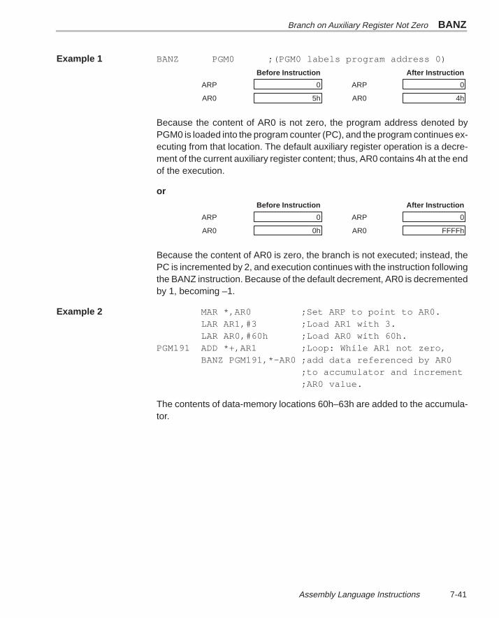
Branch on Auxiliary Register Not Zero BANZ
7-41 Assembly Language Instructions
Example 1 BANZ PGM0 ;(PGM0 labels program address 0)
Before Instruction After Instruction
ARP 0 ARP 0
AR0 5h AR0 4h
Because the content of AR0 is not zero, the program address denoted byPGM0 is loaded into the program counter (PC), and the program continues ex-ecuting from that location. The default auxiliary register operation is a decre-ment of the current auxiliary register content; thus, AR0 contains 4h at the endof the execution.
orBefore Instruction After Instruction
ARP 0 ARP 0
AR0 0h AR0 FFFFh
Because the content of AR0 is zero, the branch is not executed; instead, thePC is incremented by 2, and execution continues with the instruction followingthe BANZ instruction. Because of the default decrement, AR0 is decrementedby 1, becoming –1.
Example 2 MAR *,AR0 ;Set ARP to point to AR0.LAR AR1,#3 ;Load AR1 with 3.LAR AR0,#60h ;Load AR0 with 60h.
PGM191 ADD *+,AR1 ;Loop: While AR1 not zero,BANZ PGM191,*–AR0 ;add data referenced by AR0
;to accumulator and increment;AR0 value.
The contents of data-memory locations 60h–63h are added to the accumula-tor.
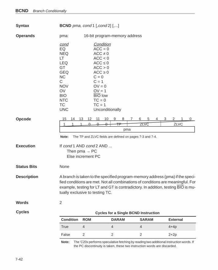
BCND Branch Conditionally
7-42
Syntax BCND pma, cond1 [,cond2] [,...]
Operands pma: 16-bit program-memory address
cond ConditionEQ ACC = 0NEQ ACC ≠ 0LT ACC < 0LEQ ACC ≤ 0GT ACC > 0GEQ ACC ≥ 0NC C = 0C C = 1NOV OV = 0OV OV = 1BIO BIO lowNTC TC = 0TC TC = 1UNC Unconditionally
Opcode 0123456789101112131415
ZLVCZLVCTP000111pma
Note: The TP and ZLVC fields are defined on pages 7-3 and 7-4.
Execution If cond1 AND cond2 AND ...Then pma → PCElse increment PC
Status Bits None
Description A branch is taken to the specified program-memory address (pma) if the speci-fied conditions are met. Not all combinations of conditions are meaningful. Forexample, testing for LT and GT is contradictory. In addition, testing BIO is mu-tually exclusive to testing TC.
Words 2
Cycles for a Single BCND Instruction
Condition ROM DARAM SARAM External
True 4 4 4 4+4p
False 2 2 2 2+2p
Note: The ’C20x performs speculative fetching by reading two additional instruction words. Ifthe PC discontinuity is taken, these two instruction words are discarded.
Cycles
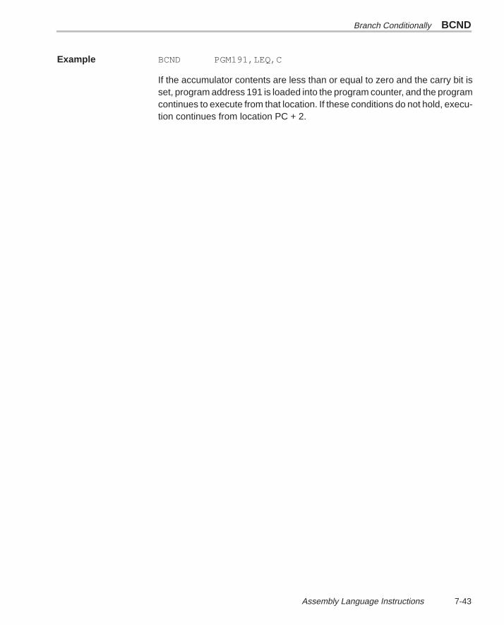
Branch Conditionally BCND
7-43 Assembly Language Instructions
Example BCND PGM191,LEQ,C
If the accumulator contents are less than or equal to zero and the carry bit isset, program address 191 is loaded into the program counter, and the programcontinues to execute from that location. If these conditions do not hold, execu-tion continues from location PC + 2.
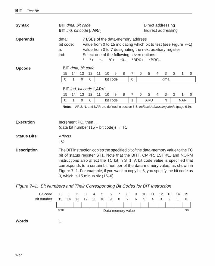
BIT Test Bit
7-44
Syntax BIT dma, bit code Direct addressingBIT ind, bit code [, ARn] Indirect addressing
Operands dma: 7 LSBs of the data-memory addressbit code: Value from 0 to 15 indicating which bit to test (see Figure 7–1)n: Value from 0 to 7 designating the next auxiliary registerind: Select one of the following seven options:
* *+ *– *0+ *0– *BR0+ *BR0–
BIT dma, bit code15 14 13 12 11 10 9 8 7 6 5 4 3 2 1 0
0 1 0 0 bit code 0 dma
BIT ind, bit code [,ARn]15 14 13 12 11 10 9 8 7 6 5 4 3 2 1 0
0 1 0 0 bit code 1 ARU N NAR
Note: ARU, N, and NAR are defined in section 6.3, Indirect Addressing Mode (page 6-9).
Execution Increment PC, then ...(data bit number (15 – bit code)) → TC
Status Bits AffectsTC
Description The BIT instruction copies the specified bit of the data-memory value to the TCbit of status register ST1. Note that the BITT, CMPR, LST #1, and NORMinstructions also affect the TC bit in ST1. A bit code value is specified thatcorresponds to a certain bit number of the data-memory value, as shown inFigure 7–1. For example, if you want to copy bit 6, you specify the bit code as9, which is 15 minus six (15–6).
Figure 7–1. Bit Numbers and Their Corresponding Bit Codes for BIT Instruction
Bit code 0 1 2 3 4 5 6 7 8 9 10 11 12 13 14 15Bit number 15 14 13 12 11 10 9 8 7 6 5 4 3 2 1 0
MSB Data-memory value LSB
Words 1
Opcode
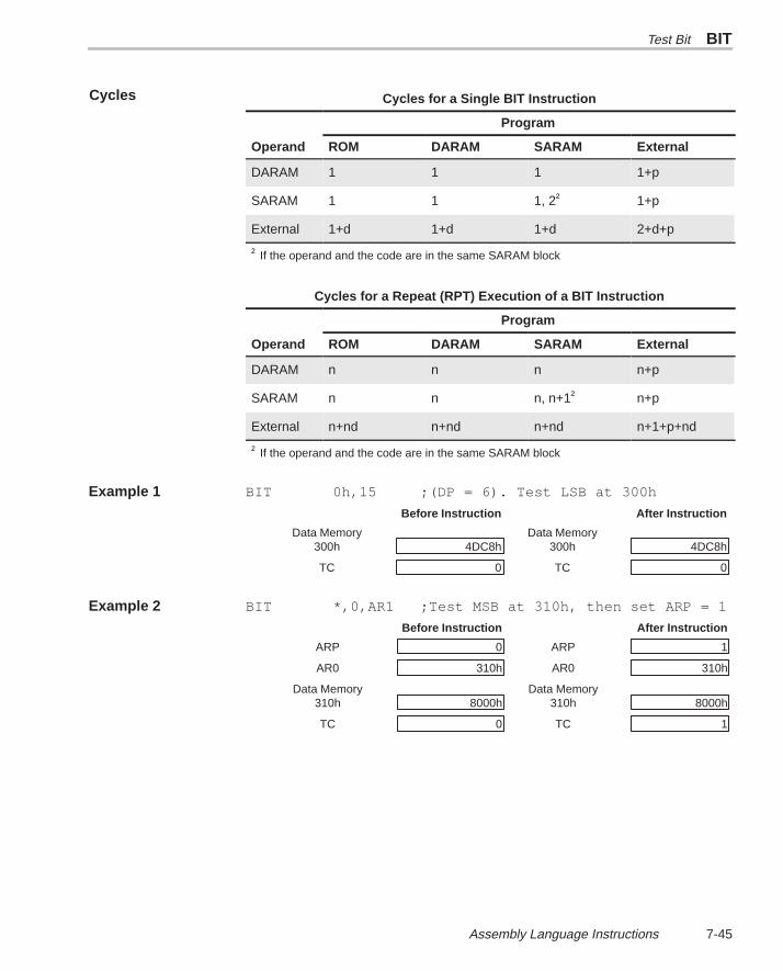
Test Bit BIT
7-45 Assembly Language Instructions
Cycles for a Single BIT Instruction
Program
Operand ROM DARAM SARAM External
DARAM 1 1 1 1+p
SARAM 1 1 1, 2† 1+p
External 1+d 1+d 1+d 2+d+p
† If the operand and the code are in the same SARAM block
Cycles for a Repeat (RPT) Execution of a BIT Instruction
Program
Operand ROM DARAM SARAM External
DARAM n n n n+p
SARAM n n n, n+1† n+p
External n+nd n+nd n+nd n+1+p+nd
† If the operand and the code are in the same SARAM block
Example 1 BIT 0h,15 ;(DP = 6). Test LSB at 300h
Before Instruction After Instruction
Data Memory Data Memory300h 4DC8h 300h 4DC8h
TC 0 TC 0
Example 2 BIT *,0,AR1 ;Test MSB at 310h, then set ARP = 1
Before Instruction After Instruction
ARP 0 ARP 1
AR0 310h AR0 310h
Data Memory Data Memory310h 8000h 310h 8000h
TC 0 TC 1
Cycles
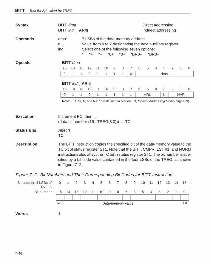
BITT Test Bit Specified by TREG
7-46
Syntax BITT dma Direct addressingBITT ind [, ARn] Indirect addressing
Operands dma: 7 LSBs of the data-memory addressn: Value from 0 to 7 designating the next auxiliary registerind: Select one of the following seven options:
* *+ *– *0+ *0– *BR0+ *BR0–
BITT dma15 14 13 12 11 10 9 8 7 6 5 4 3 2 1 0
0 1 1 0 1 1 1 1 0 dma
BITT ind [, ARn]15 14 13 12 11 10 9 8 7 6 5 4 3 2 1 0
0 1 1 0 1 1 1 1 1 ARU N NAR
Note: ARU, N, and NAR are defined in section 6.3, Indirect Addressing Mode (page 6-9).
Execution Increment PC, then ...(data bit number (15 –TREG(3:0))) → TC
Status Bits AffectsTC
Description The BITT instruction copies the specified bit of the data-memory value to theTC bit of status register ST1. Note that the BITT, CMPR, LST #1, and NORMinstructions also affect the TC bit in status register ST1. The bit number is spe-cified by a bit code value contained in the four LSBs of the TREG, as shownin Figure 7–2.
Figure 7–2. Bit Numbers and Their Corresponding Bit Codes for BITT Instruction
Bit code (in 4 LSBs ofTREG)
0 1 2 3 4 5 6 7 8 9 10 11 12 13 14 15
Bit number 15 14 13 12 11 10 9 8 7 6 5 4 3 2 1 0
MSB Data-memory value LSB
Words 1
Opcode
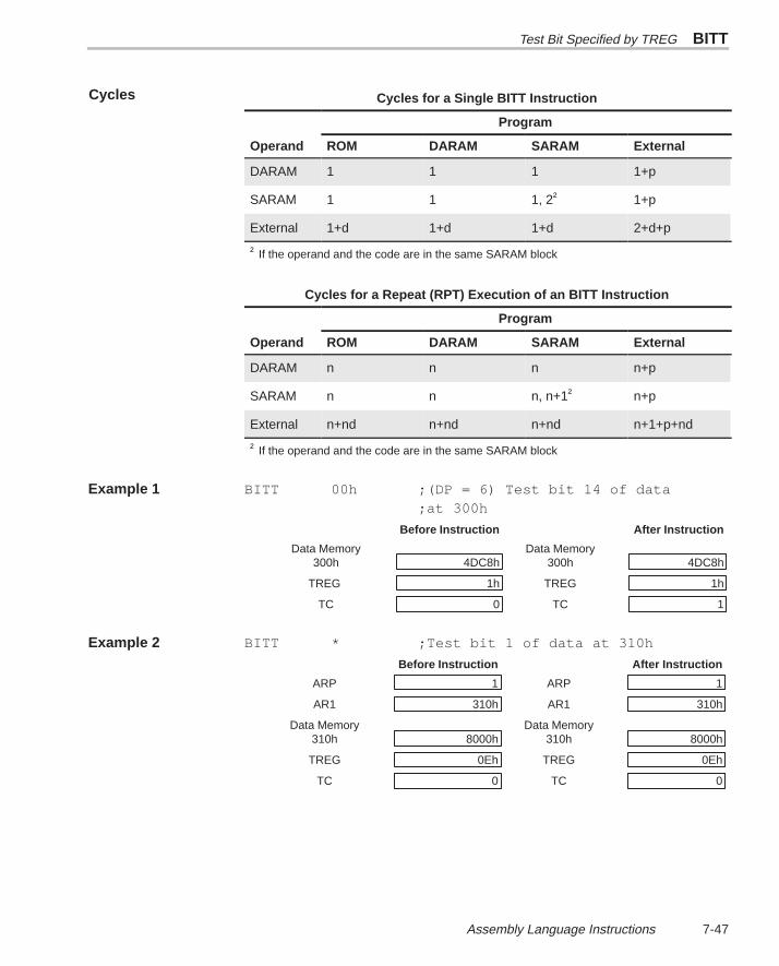
Test Bit Specified by TREG BITT
7-47 Assembly Language Instructions
Cycles for a Single BITT Instruction
Program
Operand ROM DARAM SARAM External
DARAM 1 1 1 1+p
SARAM 1 1 1, 2† 1+p
External 1+d 1+d 1+d 2+d+p
† If the operand and the code are in the same SARAM block
Cycles for a Repeat (RPT) Execution of an BITT Instruction
Program
Operand ROM DARAM SARAM External
DARAM n n n n+p
SARAM n n n, n+1† n+p
External n+nd n+nd n+nd n+1+p+nd
† If the operand and the code are in the same SARAM block
Example 1 BITT 00h ;(DP = 6) Test bit 14 of data;at 300h
Before Instruction After Instruction
Data Memory Data Memory300h 4DC8h 300h 4DC8h
TREG 1h TREG 1h
TC 0 TC 1
Example 2 BITT * ;Test bit 1 of data at 310h
Before Instruction After Instruction
ARP 1 ARP 1
AR1 310h AR1 310h
Data Memory Data Memory310h 8000h 310h 8000h
TREG 0Eh TREG 0Eh
TC 0 TC 0
Cycles
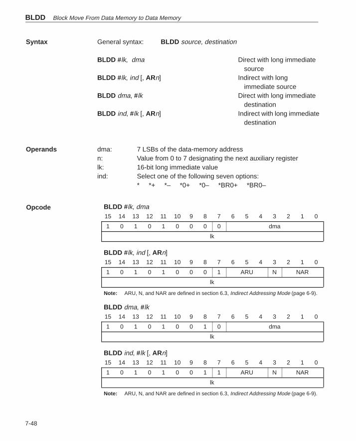
BLDD Block Move From Data Memory to Data Memory
7-48
Syntax General syntax: BLDD source, destination
BLDD #lk, dma Direct with long immediatesource
BLDD #lk, ind [, ARn] Indirect with longimmediate source
BLDD dma, #lk Direct with long immediatedestination
BLDD ind, #lk [, ARn] Indirect with long immediatedestination
Operands dma: 7 LSBs of the data-memory addressn: Value from 0 to 7 designating the next auxiliary registerlk: 16-bit long immediate valueind: Select one of the following seven options:
* *+ *– *0+ *0– *BR0+ *BR0–
BLDD # lk, dma15 14 13 12 11 10 9 8 7 6 5 4 3 2 1 0
1 0 1 0 1 0 0 0 0 dma
lk
BLDD #lk, ind [, ARn]15 14 13 12 11 10 9 8 7 6 5 4 3 2 1 0
1 0 1 0 1 0 0 0 1 ARU N NAR
lk
Note: ARU, N, and NAR are defined in section 6.3, Indirect Addressing Mode (page 6-9).
BLDD dma, #lk15 14 13 12 11 10 9 8 7 6 5 4 3 2 1 0
1 0 1 0 1 0 0 1 0 dma
lk
BLDD ind, #lk [, ARn]15 14 13 12 11 10 9 8 7 6 5 4 3 2 1 0
1 0 1 0 1 0 0 1 1 ARU N NAR
lk
Note: ARU, N, and NAR are defined in section 6.3, Indirect Addressing Mode (page 6-9).
Opcode
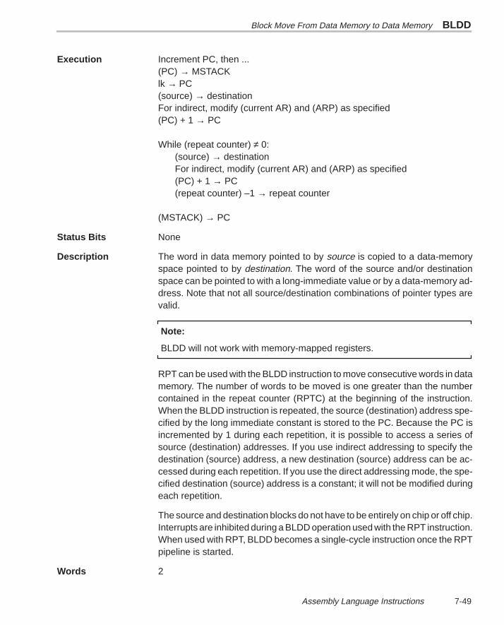
Block Move From Data Memory to Data Memory BLDD
7-49 Assembly Language Instructions
Execution Increment PC, then ...(PC) → MSTACKlk → PC(source) → destinationFor indirect, modify (current AR) and (ARP) as specified(PC) + 1 → PC
While (repeat counter) ≠ 0:(source) → destinationFor indirect, modify (current AR) and (ARP) as specified(PC) + 1 → PC(repeat counter) –1 → repeat counter
(MSTACK) → PC
Status Bits None
Description The word in data memory pointed to by source is copied to a data-memoryspace pointed to by destination. The word of the source and/or destinationspace can be pointed to with a long-immediate value or by a data-memory ad-dress. Note that not all source/destination combinations of pointer types arevalid.
Note:
BLDD will not work with memory-mapped registers.
RPT can be used with the BLDD instruction to move consecutive words in datamemory. The number of words to be moved is one greater than the numbercontained in the repeat counter (RPTC) at the beginning of the instruction.When the BLDD instruction is repeated, the source (destination) address spe-cified by the long immediate constant is stored to the PC. Because the PC isincremented by 1 during each repetition, it is possible to access a series ofsource (destination) addresses. If you use indirect addressing to specify thedestination (source) address, a new destination (source) address can be ac-cessed during each repetition. If you use the direct addressing mode, the spe-cified destination (source) address is a constant; it will not be modified duringeach repetition.
The source and destination blocks do not have to be entirely on chip or off chip.Interrupts are inhibited during a BLDD operation used with the RPT instruction.When used with RPT, BLDD becomes a single-cycle instruction once the RPTpipeline is started.
Words 2
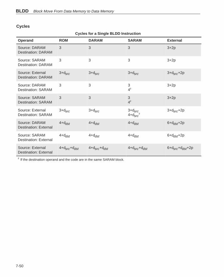
BLDD Block Move From Data Memory to Data Memory
7-50
Cycles
Cycles for a Single BLDD Instruction
Operand ROM DARAM SARAM External
Source: DARAMDestination: DARAM
3 3 3 3+2p
Source: SARAMDestination: DARAM
3 3 3 3+2p
Source: ExternalDestination: DARAM
3+dsrc 3+dsrc 3+dsrc 3+dsrc+2p
Source: DARAMDestination: SARAM
3 3 34†
3+2p
Source: SARAMDestination: SARAM
3 3 34†
3+2p
Source: ExternalDestination: SARAM
3+dsrc 3+dsrc 3+dsrc4+dsrc†
3+dsrc+2p
Source: DARAMDestination: External
4+ddst 4+ddst 4+ddst 6+ddst+2p
Source: SARAMDestination: External
4+ddst 4+ddst 4+ddst 6+ddst+2p
Source: ExternalDestination: External
4+dsrc+ddst 4+dsrc+ddst 4+dsrc+ddst 6+dsrc+ddst+2p
† If the destination operand and the code are in the same SARAM block.
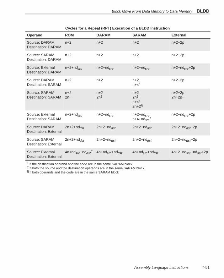
Block Move From Data Memory to Data Memory BLDD
7-51 Assembly Language Instructions
Cycles for a Repeat (RPT) Execution of a BLDD Instruction
Operand ROM DARAM SARAM External
Source: DARAMDestination: DARAM
n+2 n+2 n+2 n+2+2p
Source: SARAMDestination: DARAM
n+2 n+2 n+2 n+2+2p
Source: ExternalDestination: DARAM
n+2+ndsrc n+2+ndsrc n+2+ndsrc n+2+ndsrc+2p
Source: DARAMDestination: SARAM
n+2 n+2 n+2n+4†
n+2+2p
Source: SARAMDestination: SARAM
n+22n‡
n+22n‡
n+22n‡
n+4†
2n+2§
n+2+2p2n+2p‡
Source: ExternalDestination: SARAM
n+2+ndsrc n+2+ndsrc n+2+ndsrcn+4+ndsrc†
n+2+ndsrc+2p
Source: DARAMDestination: External
2n+2+nddst 2n+2+nddst 2n+2+nddst 2n+2+nddst+2p
Source: SARAMDestination: External
2n+2+nddst 2n+2+nddst 2n+2+nddst 2n+2+nddst+2p
Source: ExternalDestination: External
4n+ndsrc+nddst‡ 4n+ndsrc+nddst 4n+ndsrc+nddst 4n+2+ndsrc+nddst+2p
† If the destination operand and the code are in the same SARAM block‡ If both the source and the destination operands are in the same SARAM block§ If both operands and the code are in the same SARAM block
BLDD Block Move From Data Memory to Data Memory
7-52
Example 1 BLDD #300h,20h ;(DP = 6)
Before Instruction After Instruction
Data Memory Data Memory300h 0h 300h 0h
320h 0Fh 320h 0h
Example 2 BLDD *+,#321h,AR3
Before Instruction After Instruction
ARP 2 ARP 3
AR2 301h AR2 302h
Data Memory Data Memory301h 01h 301h 01h
321h 0Fh 321h 01h
Block Move From Program Memory to Data Memory BLPD
7-53 Assembly Language Instructions
Syntax General syntax: BLPD source, destination
BLPD #pma, dma Direct with long immediatesource
BLPD #pma, ind [, ARn] Indirect with long immediatesource
Operands pma: 16-bit program-memory addressdma: 7 LSBs of the data-memory addressn: Value from 0 to 7 designating the next auxiliary registerind: Select one of the following seven options:
* *+ *– *0+ *0– *BR0+ *BR0–
BLPD #pma, dma15 14 13 12 11 10 9 8 7 6 5 4 3 2 1 0
1 0 1 0 0 1 0 1 0 dma
pma
BLPD #pma, ind [, ARn]15 14 13 12 11 10 9 8 7 6 5 4 3 2 1 0
1 0 1 0 0 1 0 1 1 ARU N NAR
pma
Note: ARU, N, and NAR are defined in section 6.3, Indirect Addressing Mode (page 6-9).
Execution Increment PC, then ...(PC) → MSTACKpma → PC(source) → destinationFor indirect, modify (current AR) and (ARP) as specified(PC) + 1 → PC
While (repeat counter) ≠ 0:(source) → destinationFor indirect, modify (current AR) and (ARP) as specified(PC) + 1 → PC(repeat counter) –1 → repeat counter
(MSTACK) → PC
Status Bits None
Opcode
BLPD Block Move From Program Memory to Data Memory
7-54
Description A word in program memory pointed to by the source is copied to data-memoryspace pointed to by destination. The first word of the source space is pointedto by a long-immediate value. The data-memory destination space is pointedto by a data-memory address or auxiliary register pointer. Not all source/des-tination combinations of pointer types are valid.
RPT can be used with the BLPD instruction to move consecutive words. Thenumber of words to be moved is one greater than the number contained in therepeat counter (RPTC) at the beginning of the instruction. When the BLPD in-struction is repeated, the source (program-memory) address specified by thelong immediate constant is stored to the PC. Because the PC is incrementedby 1 during each repetition, it is possible to access a series of program-memory addresses. If you use indirect addressing to specify the destination(data-memory) address, a new data-memory address can be accessed duringeach repetition. If you use the direct addressing mode, the specified data-memory address is a constant; it will not be modified during each repetition.
The source and destination blocks do not have to be entirely on chip or off chip.Interrupts are inhibited during a repeated BLPD instruction. When used withRPT, BLPD becomes a single-cycle instruction once the RPT pipeline isstarted.
Words 2
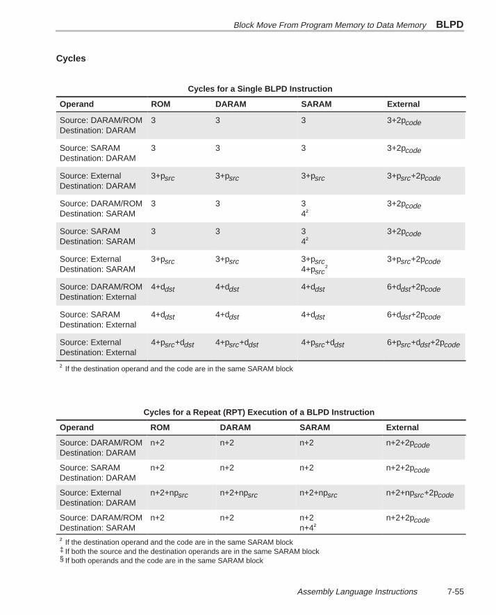
Block Move From Program Memory to Data Memory BLPD
7-55 Assembly Language Instructions
Cycles
Cycles for a Single BLPD Instruction
Operand ROM DARAM SARAM External
Source: DARAM/ROMDestination: DARAM
3 3 3 3+2pcode
Source: SARAMDestination: DARAM
3 3 3 3+2pcode
Source: ExternalDestination: DARAM
3+psrc 3+psrc 3+psrc 3+psrc+2pcode
Source: DARAM/ROMDestination: SARAM
3 3 34†
3+2pcode
Source: SARAMDestination: SARAM
3 3 34†
3+2pcode
Source: ExternalDestination: SARAM
3+psrc 3+psrc 3+psrc4+psrc†
3+psrc+2pcode
Source: DARAM/ROMDestination: External
4+ddst 4+ddst 4+ddst 6+ddst+2pcode
Source: SARAMDestination: External
4+ddst 4+ddst 4+ddst 6+ddst+2pcode
Source: ExternalDestination: External
4+psrc+ddst 4+psrc+ddst 4+psrc+ddst 6+psrc+ddst+2pcode
† If the destination operand and the code are in the same SARAM block
Cycles for a Repeat (RPT) Execution of a BLPD Instruction
Operand ROM DARAM SARAM External
Source: DARAM/ROMDestination: DARAM
n+2 n+2 n+2 n+2+2pcode
Source: SARAMDestination: DARAM
n+2 n+2 n+2 n+2+2pcode
Source: ExternalDestination: DARAM
n+2+npsrc n+2+npsrc n+2+npsrc n+2+npsrc+2pcode
Source: DARAM/ROMDestination: SARAM
n+2 n+2 n+2n+4†
n+2+2pcode
† If the destination operand and the code are in the same SARAM block‡ If both the source and the destination operands are in the same SARAM block§ If both operands and the code are in the same SARAM block
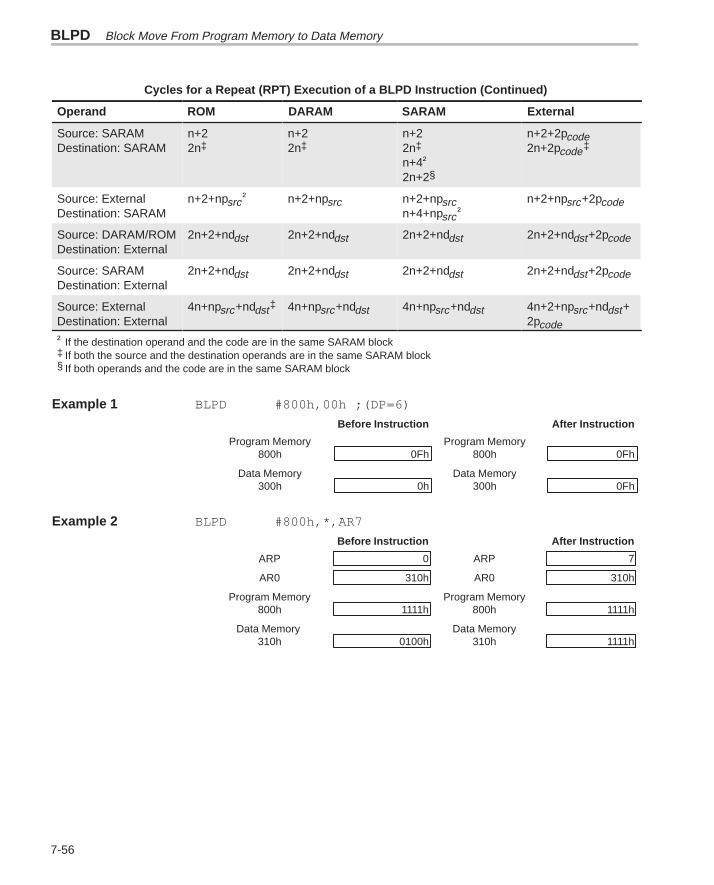
BLPD Block Move From Program Memory to Data Memory
7-56
Cycles for a Repeat (RPT) Execution of a BLPD Instruction (Continued)
Operand ExternalSARAMDARAMROM
Source: SARAMDestination: SARAM
n+22n‡
n+22n‡
n+22n‡
n+4†
2n+2§
n+2+2pcode2n+2pcode‡
Source: ExternalDestination: SARAM
n+2+npsrc† n+2+npsrc n+2+npsrcn+4+npsrc†
n+2+npsrc+2pcode
Source: DARAM/ROMDestination: External
2n+2+nddst 2n+2+nddst 2n+2+nddst 2n+2+nddst+2pcode
Source: SARAMDestination: External
2n+2+nddst 2n+2+nddst 2n+2+nddst 2n+2+nddst+2pcode
Source: ExternalDestination: External
4n+npsrc+nddst‡ 4n+npsrc+nddst 4n+npsrc+nddst 4n+2+npsrc+nddst+2pcode
† If the destination operand and the code are in the same SARAM block‡ If both the source and the destination operands are in the same SARAM block§ If both operands and the code are in the same SARAM block
Example 1 BLPD #800h,00h ;(DP=6)
Before Instruction After Instruction
Program Memory Program Memory800h 0Fh 800h 0Fh
Data Memory Data Memory300h 0h 300h 0Fh
Example 2 BLPD #800h,*,AR7
Before Instruction After Instruction
ARP 0 ARP 7
AR0 310h AR0 310h
Program Memory Program Memory800h 1111h 800h 1111h
Data Memory Data Memory310h 0100h 310h 1111h
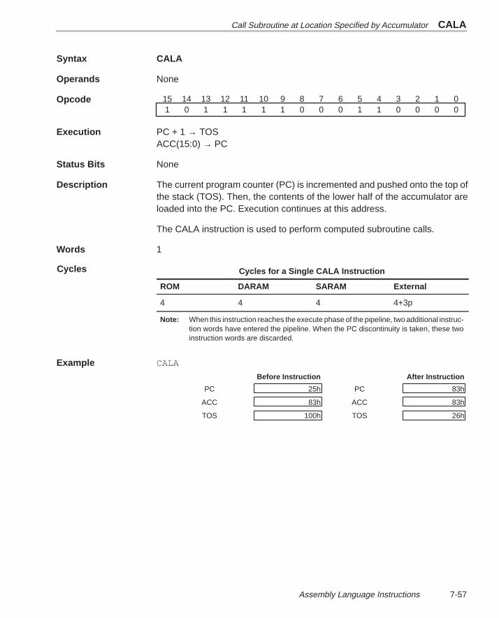
Call Subroutine at Location Specified by Accumulator CALA
7-57 Assembly Language Instructions
Syntax CALA
Operands None
Opcode 01234567891011121314150000110001111101
Execution PC + 1 → TOSACC(15:0) → PC
Status Bits None
Description The current program counter (PC) is incremented and pushed onto the top ofthe stack (TOS). Then, the contents of the lower half of the accumulator areloaded into the PC. Execution continues at this address.
The CALA instruction is used to perform computed subroutine calls.
Words 1
Cycles for a Single CALA Instruction
ROM DARAM SARAM External
4 4 4 4+3p
Note: When this instruction reaches the execute phase of the pipeline, two additional instruc-tion words have entered the pipeline. When the PC discontinuity is taken, these twoinstruction words are discarded.
Example CALA
Before Instruction After Instruction
PC 25h PC 83h
ACC 83h ACC 83h
TOS 100h TOS 26h
Cycles
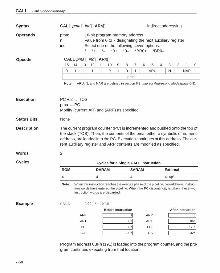
CALL Call Unconditionally
7-58
Syntax CALL pma [, ind [, ARn]] Indirect addressing
Operands pma: 16-bit program-memory addressn: Value from 0 to 7 designating the next auxiliary registerind: Select one of the following seven options:
* *+ *– *0+ *0– *BR0+ *BR0–
CALL pma [, ind [, ARn]]15 14 13 12 11 10 9 8 7 6 5 4 3 2 1 0
0 1 1 1 1 0 1 0 1 ARU N NAR
pma
Note: ARU, N, and NAR are defined in section 6.3, Indirect Addressing Mode (page 6-9).
Execution PC + 2 → TOSpma → PCModify (current AR) and (ARP) as specified.
Status Bits None
Description The current program counter (PC) is incremented and pushed onto the top ofthe stack (TOS). Then, the contents of the pma, either a symbolic or numericaddress, are loaded into the PC. Execution continues at this address. The cur-rent auxiliary register and ARP contents are modified as specified.
Words 2
Cycles for a Single CALL Instruction
ROM DARAM SARAM External
4 4 4 4+4p†
Note: When this instruction reaches the execute phase of the pipeline, two additional instruc-tion words have entered the pipeline. When the PC discontinuity is taken, these twoinstruction words are discarded.
Example CALL 191,*+,AR0
Before Instruction After Instruction
ARP 1 ARP 0
AR1 05h AR1 06h
PC 30h PC 0BFh
TOS 100h TOS 32h
Program address 0BFh (191) is loaded into the program counter, and the pro-gram continues executing from that location.
Opcode
Cycles
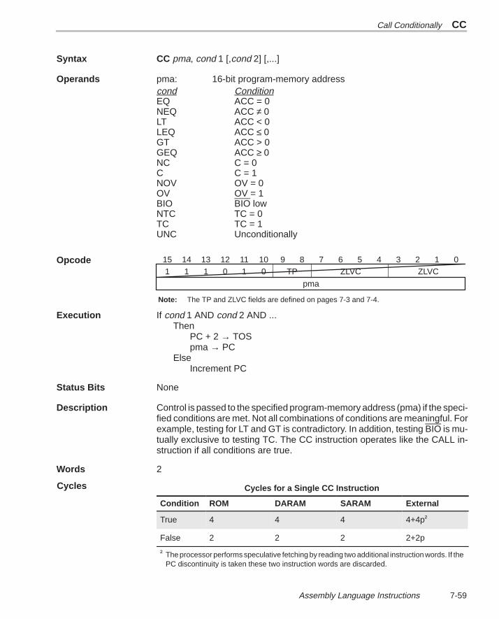
Call Conditionally CC
7-59 Assembly Language Instructions
Syntax CC pma, cond1 [,cond2] [,...]
Operands pma: 16-bit program-memory addresscond ConditionEQ ACC = 0NEQ ACC ≠ 0LT ACC < 0LEQ ACC ≤ 0GT ACC > 0GEQ ACC ≥ 0NC C = 0C C = 1NOV OV = 0OV OV = 1BIO BIO lowNTC TC = 0TC TC = 1UNC Unconditionally
Opcode 0123456789101112131415ZLVCZLVCTP010111
pma
Note: The TP and ZLVC fields are defined on pages 7-3 and 7-4.
Execution If cond1 AND cond2 AND ...Then
PC + 2 → TOSpma → PC
ElseIncrement PC
Status Bits None
Description Control is passed to the specified program-memory address (pma) if the speci-fied conditions are met. Not all combinations of conditions are meaningful. Forexample, testing for LT and GT is contradictory. In addition, testing BIO is mu-tually exclusive to testing TC. The CC instruction operates like the CALL in-struction if all conditions are true.
Words 2
Cycles for a Single CC Instruction
Condition ROM DARAM SARAM External
True 4 4 4 4+4p†
False 2 2 2 2+2p
† The processor performs speculative fetching by reading two additional instruction words. If thePC discontinuity is taken these two instruction words are discarded.
Cycles
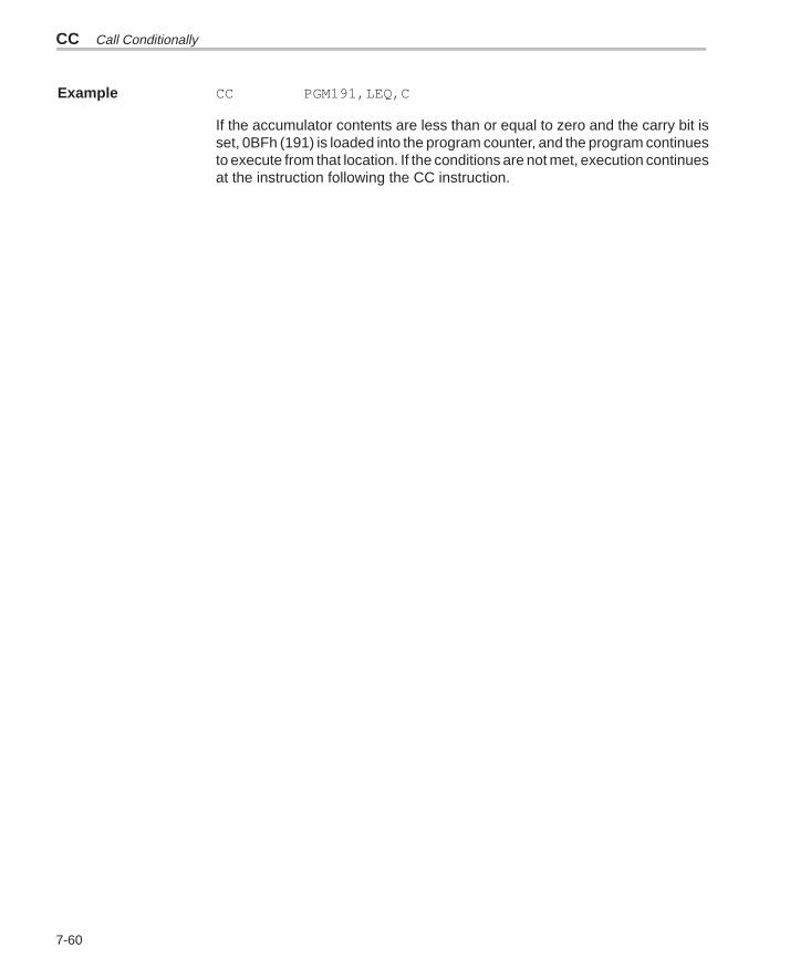
CC Call Conditionally
7-60
Example CC PGM191,LEQ,C
If the accumulator contents are less than or equal to zero and the carry bit isset, 0BFh (191) is loaded into the program counter, and the program continuesto execute from that location. If the conditions are not met, execution continuesat the instruction following the CC instruction.
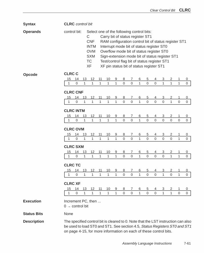
Clear Control Bit CLRC
7-61 Assembly Language Instructions
Syntax CLRC control bit
Operands control bit: Select one of the following control bits:C Carry bit of status register ST1CNF RAM configuration control bit of status register ST1INTM Interrupt mode bit of status register ST0OVM Overflow mode bit of status register ST0SXM Sign-extension mode bit of status register ST1TC Test/control flag bit of status register ST1XF XF pin status bit of status register ST1
CLRC C01234567891011121314150111001001111101
CLRC CNF01234567891011121314150010001001111101
CLRC INTM01234567891011121314150000001001111101
CLRC OVM01234567891011121314150100001001111101
CLRC SXM01234567891011121314150110001001111101
CLRC TC01234567891011121314150101001001111101
CLRC XF01234567891011121314150011001001111101
Execution Increment PC, then ...0 → control bit
Status Bits None
Description The specified control bit is cleared to 0. Note that the LST instruction can alsobe used to load ST0 and ST1. See section 4.5, Status Registers ST0 and ST1on page 4-15, for more information on each of these control bits.
Opcode
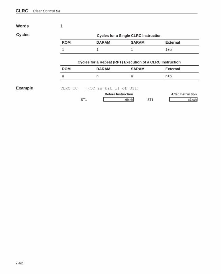
CLRC Clear Control Bit
7-62
Words 1
Cycles for a Single CLRC Instruction
ROM DARAM SARAM External
1 1 1 1+p
Cycles for a Repeat (RPT) Execution of a CLRC Instruction
ROM DARAM SARAM External
n n n n+p
Example CLRC TC ;(TC is bit 11 of ST1)
Before Instruction After Instruction
ST1 x9xxh ST1 x1xxh
Cycles
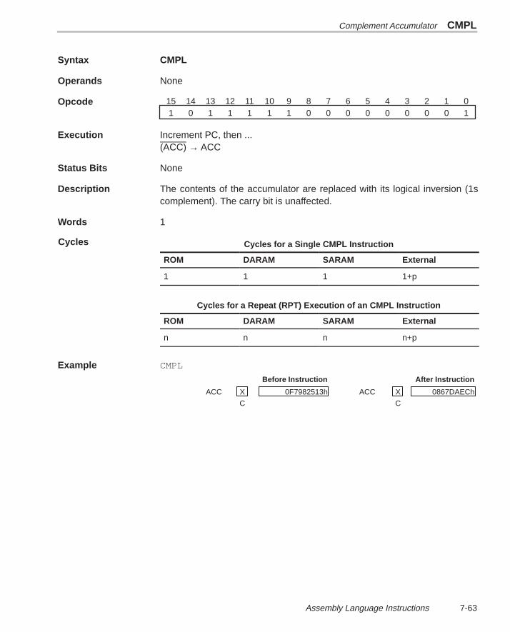
Complement Accumulator CMPL
7-63 Assembly Language Instructions
Syntax CMPL
Operands None
Opcode 01234567891011121314151000000001111101
Execution Increment PC, then ...(ACC) → ACC
Status Bits None
Description The contents of the accumulator are replaced with its logical inversion (1scomplement). The carry bit is unaffected.
Words 1
Cycles for a Single CMPL Instruction
ROM DARAM SARAM External
1 1 1 1+p
Cycles for a Repeat (RPT) Execution of an CMPL Instruction
ROM DARAM SARAM External
n n n n+p
Example CMPL
Before Instruction After Instruction
ACC X 0F7982513h ACC X 0867DAECh
C C
Cycles
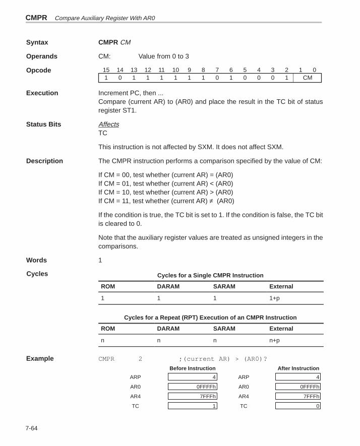
CMPR Compare Auxiliary Register With AR0
7-64
Syntax CMPR CM
Operands CM: Value from 0 to 3
Opcode 0123456789101112131415CM10001011111101
Execution Increment PC, then ...Compare (current AR) to (AR0) and place the result in the TC bit of statusregister ST1.
Status Bits AffectsTC
This instruction is not affected by SXM. It does not affect SXM.
Description The CMPR instruction performs a comparison specified by the value of CM:
If CM = 00, test whether (current AR) = (AR0)If CM = 01, test whether (current AR) < (AR0)If CM = 10, test whether (current AR) > (AR0)If CM = 11, test whether (current AR) ≠ (AR0)
If the condition is true, the TC bit is set to 1. If the condition is false, the TC bitis cleared to 0.
Note that the auxiliary register values are treated as unsigned integers in thecomparisons.
Words 1
Cycles for a Single CMPR Instruction
ROM DARAM SARAM External
1 1 1 1+p
Cycles for a Repeat (RPT) Execution of an CMPR Instruction
ROM DARAM SARAM External
n n n n+p
Example CMPR 2 ;(current AR) > (AR0)?
Before Instruction After Instruction
ARP 4 ARP 4
AR0 0FFFFh AR0 0FFFFh
AR4 7FFFh AR4 7FFFh
TC 1 TC 0
Cycles
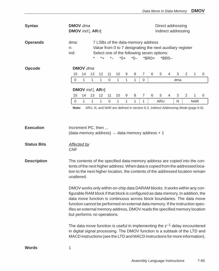
Data Move in Data Memory DMOV
7-65 Assembly Language Instructions
Syntax DMOV dma Direct addressingDMOV ind [, ARn] Indirect addressing
Operands dma: 7 LSBs of the data-memory addressn: Value from 0 to 7 designating the next auxiliary registerind: Select one of the following seven options:
* *+ *– *0+ *0– *BR0+ *BR0–
DMOV dma15 14 13 12 11 10 9 8 7 6 5 4 3 2 1 0
0 1 1 1 0 1 1 1 0 dma
DMOV ind [, ARn]15 14 13 12 11 10 9 8 7 6 5 4 3 2 1 0
0 1 1 1 0 1 1 1 1 ARU N NAR
Note: ARU, N, and NAR are defined in section 6.3, Indirect Addressing Mode (page 6-9).
Execution Increment PC, then ...(data-memory address) → data-memory address + 1
Status Bits Affected byCNF
Description The contents of the specified data-memory address are copied into the con-tents of the next higher address. When data is copied from the addressed loca-tion to the next higher location, the contents of the addressed location remainunaltered.
DMOV works only within on-chip data DARAM blocks. It works within any con-figurable RAM block if that block is configured as data memory. In addition, thedata move function is continuous across block boundaries. The data movefunction cannot be performed on external data memory. If the instruction spec-ifies an external memory address, DMOV reads the specified memory locationbut performs no operations.
The data move function is useful in implementing the z–1 delay encounteredin digital signal processing. The DMOV function is a subtask of the LTD andMACD instructions (see the LTD and MACD instructions for more information).
Words 1
Opcode
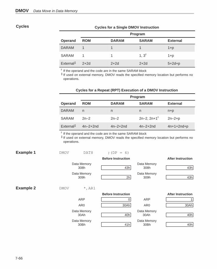
DMOV Data Move in Data Memory
7-66
Cycles for a Single DMOV Instruction
Program
Operand ROM DARAM SARAM External
DARAM 1 1 1 1+p
SARAM 1 1 1, 3† 1+p
External‡ 2+2d 2+2d 2+2d 5+2d+p
† If the operand and the code are in the same SARAM block‡ If used on external memory, DMOV reads the specified memory location but performs no
operations.
Cycles for a Repeat (RPT) Execution of a DMOV Instruction
Program
Operand ROM DARAM SARAM External
DARAM n n n n+p
SARAM 2n–2 2n–2 2n–2, 2n+1† 2n–2+p
External‡ 4n–2+2nd 4n–2+2nd 4n–2+2nd 4n+1+2nd+p
† If the operand and the code are in the same SARAM block‡ If used on external memory, DMOV reads the specified memory location but performs no
operations.
Example 1 DMOV DAT8 ;(DP = 6)
Before Instruction After Instruction
Data Memory Data Memory308h 43h 308h 43h
Data Memory Data Memory309h 2h 309h 43h
Example 2 DMOV *,AR1
Before Instruction After Instruction
ARP 0 ARP 1
AR0 30Ah AR0 30Ah
Data Memory Data Memory30Ah 40h 30Ah 40h
Data Memory Data Memory30Bh 41h 30Bh 40h
Cycles
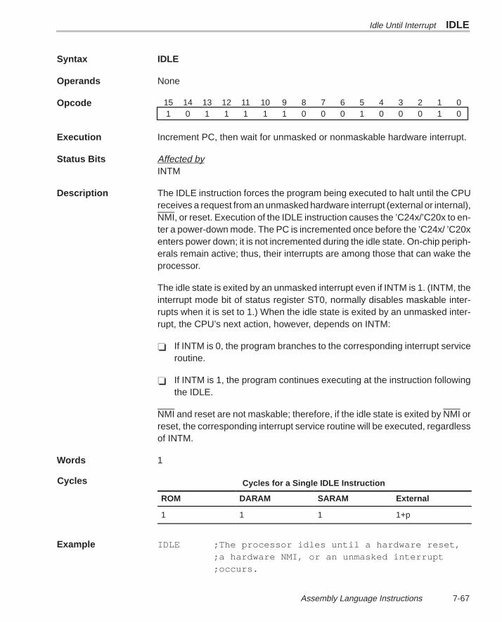
Idle Until Interrupt IDLE
7-67 Assembly Language Instructions
Syntax IDLE
Operands None
Opcode 01234567891011121314150100010001111101
Execution Increment PC, then wait for unmasked or nonmaskable hardware interrupt.
Status Bits Affected by INTM
Description The IDLE instruction forces the program being executed to halt until the CPUreceives a request from an unmasked hardware interrupt (external or internal),NMI, or reset. Execution of the IDLE instruction causes the ’C24x/’C20x to en-ter a power-down mode. The PC is incremented once before the ’C24x/ ’C20xenters power down; it is not incremented during the idle state. On-chip periph-erals remain active; thus, their interrupts are among those that can wake theprocessor.
The idle state is exited by an unmasked interrupt even if INTM is 1. (INTM, theinterrupt mode bit of status register ST0, normally disables maskable inter-rupts when it is set to 1.) When the idle state is exited by an unmasked inter-rupt, the CPU’s next action, however, depends on INTM:
If INTM is 0, the program branches to the corresponding interrupt serviceroutine.
If INTM is 1, the program continues executing at the instruction followingthe IDLE.
NMI and reset are not maskable; therefore, if the idle state is exited by NMI orreset, the corresponding interrupt service routine will be executed, regardlessof INTM.
Words 1
Cycles for a Single IDLE Instruction
ROM DARAM SARAM External
1 1 1 1+p
Example IDLE ;The processor idles until a hardware reset,;a hardware NMI, or an unmasked interrupt;occurs.
Cycles
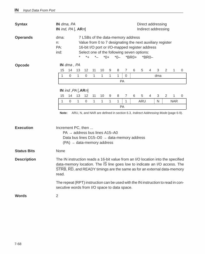
IN Input Data From Port
7-68
Syntax IN dma, PA Direct addressingIN ind, PA [, ARn] Indirect addressing
Operands dma: 7 LSBs of the data-memory addressn: Value from 0 to 7 designating the next auxiliary registerPA: 16-bit I/O port or I/O-mapped register addressind: Select one of the following seven options:
* *+ *– *0+ *0– *BR0+ *BR0–
IN dma , PA15 14 13 12 11 10 9 8 7 6 5 4 3 2 1 0
1 0 1 0 1 1 1 1 0 dma
PA
IN ind ,PA [,ARn]15 14 13 12 11 10 9 8 7 6 5 4 3 2 1 0
1 0 1 0 1 1 1 1 1 ARU N NAR
PA
Note: ARU, N, and NAR are defined in section 6.3, Indirect Addressing Mode (page 6-9).
Execution Increment PC, then ...PA → address bus lines A15–A0Data bus lines D15–D0 → data-memory address(PA) → data-memory address
Status Bits None
Description The IN instruction reads a 16-bit value from an I/O location into the specifieddata-memory location. The IS line goes low to indicate an I/O access. TheSTRB, RD, and READY timings are the same as for an external data-memoryread.
The repeat (RPT) instruction can be used with the IN instruction to read in con-secutive words from I/O space to data space.
Words 2
Opcode
Input Data From Port IN
7-69 Assembly Language Instructions
Cycles for a Single IN Instruction
Program
Operand ROM DARAM SARAM External
Destination: DARAM 2+iosrc 2+iosrc 2+iosrc 3+iosrc+2pcode
Destination: SARAM 2+iosrc 2+iosrc 2+iosrc3+iosrc†
3+iosrc+2pcode
Destination: External 3+ddst+iosrc 3+ddst+iosrc 3+ddst+iosrc 6+ddst+iosrc+2pcode
† If the operand and the code are in the same SARAM block
Cycles for a Repeat (RPT) Execution of an IN Instruction
Program
Operand ROM DARAM SARAM External
Destination: DARAM 2n+niosrc 2n+niosrc 2n+niosrc 2n+1+niosrc+2pcode
Destination: SARAM 2n+niosrc 2n+niosrc 2n+niosrc2n+2+niosrc†
2n+1+niosrc+2pcode
Destination: External 4n–1+nddst+niosrc
4n–1+nddst+niosrc 4n–1+nddst+niosrc 4n+2+nddst+niosrc+2pcode
† If the operand and the code are in the same SARAM block
Example 1 IN 7,1000h ;Read in word from peripheral on;port address 1000h. Store word in;data memory location 307h (DP=6).
Example 2 IN *,5h ;Read in word from peripheral on;port address 5h. Store word in;data memory location specified by;current auxiliary register.
Cycles
INTR Software Interrupt
7-70
Syntax INTR K
Operands K: Value from 0 to 31 that indicates the interrupt vector locationto branch to
Opcode 0123456789101112131415K11001111101
Execution (PC) + 1 → stackcorresponding interrupt vector location → PC
Status Bits AffectsINTM
This instruction is not affected by INTM.
Description The processor has locations for 32 interrupt vectors; each location is repre-sented by a value K from 0 to 31. The INTR instruction is a software interruptthat transfers program control to the program-memory address specified byK. The vector at that address then leads to the corresponding interrupt serviceroutine. Thus, the instruction allows any one of the interrupt service routinesto be executed from your software. For a list of interrupts and their correspond-ing K values, see Table 5–5 on page 5-15. During execution of the instruction,the value PC + 1 (the return address) is pushed onto the stack. Neither theINTM bit nor the interrupt masks affect the INTR instruction. An INTR for theexternal interrupts looks exactly like an external interrupt (an interrupt ac-knowledge is generated, and maskable interrupts are globally disabled by set-ting INTM = 1).
Words 1
Cycles for a Single INTR Instruction
ROM DARAM SARAM External
4 4 4 4+3p†
† The processor performs speculative fetching by reading two additional instruction words. If thePC discontinuity is taken, these two instruction words are discarded.
Example INTR 3 ;PC + 1 is pushed onto the stack.;Then control is passed to program;memory location 6h.
Cycles
Load Accumulator With Shift LACC
7-71 Assembly Language Instructions
Syntax LACC dma [, shift] Direct addressingLACC dma, 16 Direct with left shift of 16LACC ind [, shift [, ARn]] Indirect addressingLACC ind, 16[, ARn] Indirect with left shift of 16LACC #lk [, shift] Long immediate addressing
Operands dma: 7 LSBs of the data-memory addressshift: Left shift value from 0 to 15 (defaults to 0)n: Value from 0 to 7 designating the next auxiliary registerlk: 16-bit long immediate valueind: Select one of the following seven options:
* *+ *– *0+ *0– *BR0+ *BR0–
LACC dma [ , shift ]15 14 13 12 11 10 9 8 7 6 5 4 3 2 1 0
0 0 0 1 shift 0 dma
LACC dma, 1615 14 13 12 11 10 9 8 7 6 5 4 3 2 1 0
0 1 1 0 1 0 1 0 0 dma
LACC ind [, shift[, ARn]]15 14 13 12 11 10 9 8 7 6 5 4 3 2 1 0
0 0 0 1 shift 1 ARU N NAR
Note: ARU, N, and NAR are defined in section 6.3, Indirect Addressing Mode (page 6-9).
LACC ind, 16[, ARn]15 14 13 12 11 10 9 8 7 6 5 4 3 2 1 0
0 1 1 0 1 0 1 0 1 ARU N NAR
Note: ARU, N, and NAR are defined in section 6.3, Indirect Addressing Mode (page 6-9).
LACC #lk [, shift]15 14 13 12 11 10 9 8 7 6 5 4 3 2 1 0
1 0 1 1 1 1 1 1 1 0 0 0 shift
lk
Opcode
LACC Load Accumulator With Shift
7-72
Execution Increment PC, then ...Event Addressing mode(data-memory address) × 2shift → ACC Direct or indirect
(data-memory address) × 216 → ACC Direct or indirect (shift of 16)
lk × 2shift → ACC Long immediate
Status Bits Affected bySXM
Description The contents of the specified data-memory address or a 16-bit constant areleft shifted and loaded into the accumulator. During shifting, low-order bits arezero filled. High-order bits are sign extended if SXM = 1 and zeroed if SXM = 0.
Words Words Addressing mode1 Direct or indirect
2 Long immediate
Cycles for a Single LACC Instruction (Using Direct and Indirect Addressing)
Program
Operand ROM DARAM SARAM External
DARAM 1 1 1 1+p
SARAM 1 1 1, 2† 1+p
External 1+d 1+d 1+d 2+d+p
† If the operand and the code are in the same SARAM block
Cycles for a Repeat (RPT) Execution of an LACC Instruction (Using Directand Indirect Addressing)
Program
Operand ROM DARAM SARAM External
DARAM n n n n+p
SARAM n n n, n+1† n+p
External n+nd n+nd n+nd n+1+p+nd
† If the operand and the code are in the same SARAM block
Cycles for a Single LACC Instruction (Using Immediate Addressing)
ROM DARAM SARAM External
2 2 2 2+2p
Cycles
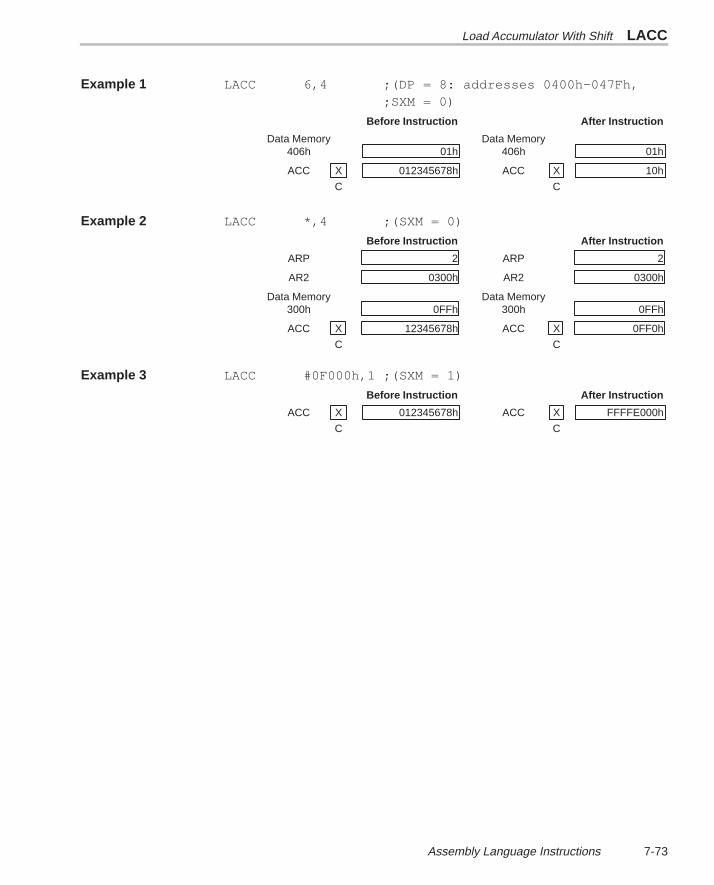
Load Accumulator With Shift LACC
7-73 Assembly Language Instructions
Example 1 LACC 6,4 ;(DP = 8: addresses 0400h–047Fh,;SXM = 0)
Before Instruction After Instruction
Data Memory Data Memory406h 01h 406h 01h
ACC X 012345678h ACC X 10h
C C
Example 2 LACC *,4 ;(SXM = 0)
Before Instruction After Instruction
ARP 2 ARP 2
AR2 0300h AR2 0300h
Data Memory Data Memory300h 0FFh 300h 0FFh
ACC X 12345678h ACC X 0FF0h
C C
Example 3 LACC #0F000h,1 ;(SXM = 1)
Before Instruction After Instruction
ACC X 012345678h ACC X FFFFE000h
C C

LACL Load Low Accumulator and Clear High Accumulator
7-74
Syntax LACL dma Direct addressingLACL ind [, ARn] Indirect addressingLACL #k Short immediate
Operands dma: 7 LSBs of the data-memory addressn: Value from 0 to 7 designating the next auxiliary registerk: 8-bit short immediate valueind: Select one of the following seven options:
* *+ *– *0+ *0– *BR0+ *BR0–
LACL dma15 14 13 12 11 10 9 8 7 6 5 4 3 2 1 0
0 1 1 0 1 0 0 1 0 dma
LACL ind [, ARn]15 14 13 12 11 10 9 8 7 6 5 4 3 2 1 0
0 1 1 0 1 0 0 1 1 ARU N NAR
Note: ARU, N, and NAR are defined in section 6.3, Indirect Addressing Mode (page 6-9).
LACL #k15 14 13 12 11 10 9 8 7 6 5 4 3 2 1 0
1 0 1 1 1 0 0 1 k
Execution Increment PC, then ...Events Addressing mode0 → ACC(31:16) Direct or indirect(data-memory address) → ACC(15:0)
0 → ACC(31:8) Short immediatek → ACC(7:0)
Status Bits This instruction is not affected by SXM.
Description The contents of the addressed data-memory location or a zero-extended 8-bitconstant are loaded into the 16 low-order bits of the accumulator. The upperhalf of the accumulator is zeroed. The data is treated as an unsigned 16-bitnumber rather than a 2s-complement number. There is no sign extension ofthe operand with this instruction, regardless of the state of SXM.
Words 1
Opcode
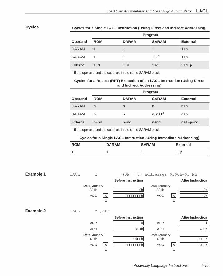
Load Low Accumulator and Clear High Accumulator LACL
7-75 Assembly Language Instructions
Cycles for a Single LACL Instruction (Using Direct and Indirect Addressing)
Program
Operand ROM DARAM SARAM External
DARAM 1 1 1 1+p
SARAM 1 1 1, 2† 1+p
External 1+d 1+d 1+d 2+d+p
† If the operand and the code are in the same SARAM block
Cycles for a Repeat (RPT) Execution of an LACL Instruction (Using Directand Indirect Addressing)
Program
Operand ROM DARAM SARAM External
DARAM n n n n+p
SARAM n n n, n+1† n+p
External n+nd n+nd n+nd n+1+p+nd
† If the operand and the code are in the same SARAM block
Cycles for a Single LACL Instruction (Using Immediate Addressing)
ROM DARAM SARAM External
1 1 1 1+p
Example 1 LACL 1 ;(DP = 6: addresses 0300h–037Fh)
Before Instruction After Instruction
Data Memory Data Memory301h 0h 301h 0h
ACC X 7FFFFFFFh ACC X 0h
C C
Example 2 LACL *–,AR4
Before Instruction After Instruction
ARP 0 ARP 4
AR0 401h AR0 400h
Data Memory Data Memory401h 00FFh 401h 00FFh
ACC X 7FFFFFFFh ACC X 0FFh
C C
Cycles
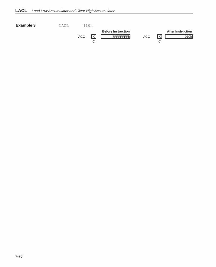
LACL Load Low Accumulator and Clear High Accumulator
7-76
Example 3 LACL #10h
Before Instruction After Instruction
ACC X 7FFFFFFFh ACC X 010h
C C
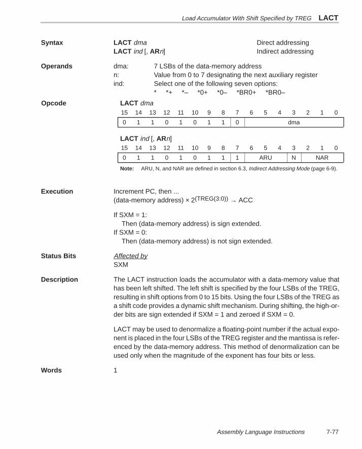
Load Accumulator With Shift Specified by TREG LACT
7-77 Assembly Language Instructions
Syntax LACT dma Direct addressingLACT ind [, ARn] Indirect addressing
Operands dma: 7 LSBs of the data-memory addressn: Value from 0 to 7 designating the next auxiliary registerind: Select one of the following seven options:
* *+ *– *0+ *0– *BR0+ *BR0–
LACT dma15 14 13 12 11 10 9 8 7 6 5 4 3 2 1 0
0 1 1 0 1 0 1 1 0 dma
LACT ind [, ARn]15 14 13 12 11 10 9 8 7 6 5 4 3 2 1 0
0 1 1 0 1 0 1 1 1 ARU N NAR
Note: ARU, N, and NAR are defined in section 6.3, Indirect Addressing Mode (page 6-9).
Execution Increment PC, then ...(data-memory address) × 2(TREG(3:0)) → ACC
If SXM = 1:Then (data-memory address) is sign extended.
If SXM = 0:Then (data-memory address) is not sign extended.
Status Bits Affected bySXM
Description The LACT instruction loads the accumulator with a data-memory value thathas been left shifted. The left shift is specified by the four LSBs of the TREG,resulting in shift options from 0 to 15 bits. Using the four LSBs of the TREG asa shift code provides a dynamic shift mechanism. During shifting, the high-or-der bits are sign extended if SXM = 1 and zeroed if SXM = 0.
LACT may be used to denormalize a floating-point number if the actual expo-nent is placed in the four LSBs of the TREG register and the mantissa is refer-enced by the data-memory address. This method of denormalization can beused only when the magnitude of the exponent has four bits or less.
Words 1
Opcode
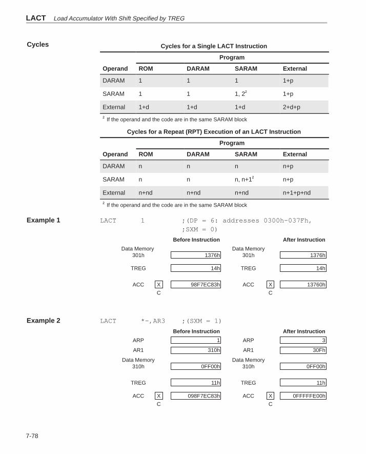
LACT Load Accumulator With Shift Specified by TREG
7-78
Cycles for a Single LACT Instruction
Program
Operand ROM DARAM SARAM External
DARAM 1 1 1 1+p
SARAM 1 1 1, 2† 1+p
External 1+d 1+d 1+d 2+d+p
† If the operand and the code are in the same SARAM block
Cycles for a Repeat (RPT) Execution of an LACT Instruction
Program
Operand ROM DARAM SARAM External
DARAM n n n n+p
SARAM n n n, n+1† n+p
External n+nd n+nd n+nd n+1+p+nd
† If the operand and the code are in the same SARAM block
Example 1 LACT 1 ;(DP = 6: addresses 0300h–037Fh,;SXM = 0)
Before Instruction After Instruction
Data Memory Data Memory301h 1376h 301h 1376h
TREG 14h TREG 14h
ACC X 98F7EC83h ACC X 13760h
C C
Example 2 LACT *–,AR3 ;(SXM = 1)
Before Instruction After Instruction
ARP 1 ARP 3
AR1 310h AR1 30Fh
Data Memory Data Memory310h 0FF00h 310h 0FF00h
TREG 11h TREG 11h
ACC X 098F7EC83h ACC X 0FFFFFE00h
C C
Cycles
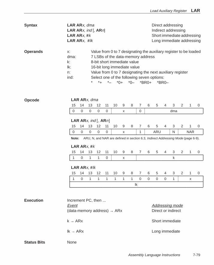
Load Auxiliary Register LAR
7-79 Assembly Language Instructions
Syntax LAR ARx, dma Direct addressingLAR ARx, ind [, ARn] Indirect addressingLAR ARx, #k Short immediate addressingLAR ARx, #lk Long immediate addressing
Operands x: Value from 0 to 7 designating the auxiliary register to be loadeddma: 7 LSBs of the data-memory addressk: 8-bit short immediate valuelk: 16-bit long immediate valuen: Value from 0 to 7 designating the next auxiliary registerind: Select one of the following seven options:
* *+ *– *0+ *0– *BR0+ *BR0–
LAR AR x, dma15 14 13 12 11 10 9 8 7 6 5 4 3 2 1 0
0 0 0 0 0 x 0 dma
LAR AR x, ind [, ARn]15 14 13 12 11 10 9 8 7 6 5 4 3 2 1 0
0 0 0 0 0 x 1 ARU N NAR
Note: ARU, N, and NAR are defined in section 6.3, Indirect Addressing Mode (page 6-9).
LAR AR x, #k15 14 13 12 11 10 9 8 7 6 5 4 3 2 1 0
1 0 1 1 0 x k
LAR AR x, #lk15 14 13 12 11 10 9 8 7 6 5 4 3 2 1 0
1 0 1 1 1 1 1 1 0 0 0 0 1 x
lk
Execution Increment PC, then ...Event Addressing mode(data-memory address) → ARx Direct or indirect
k → ARx Short immediate
lk → ARx Long immediate
Status Bits None
Opcode
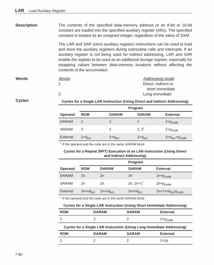
LAR Load Auxiliary Register
7-80
Description The contents of the specified data-memory address or an 8-bit or 16-bitconstant are loaded into the specified auxiliary register (ARx). The specifiedconstant is treated as an unsigned integer, regardless of the value of SXM.
The LAR and SAR (store auxiliary register) instructions can be used to loadand store the auxiliary registers during subroutine calls and interrupts. If anauxiliary register is not being used for indirect addressing, LAR and SARenable the register to be used as an additional storage register, especially forswapping values between data-memory locations without affecting thecontents of the accumulator.
Words Words Addressing mode1 Direct, indirect or
short immediate2 Long immediate
Cycles for a Single LAR Instruction (Using Direct and Indirect Addressing)
Program
Operand ROM DARAM SARAM External
DARAM 2 2 2 2+pcode
SARAM 2 2 2, 3† 2+pcode
External 2+dsrc 2+dsrc 2+dsrc 3+dsrc+pcode
† If the operand and the code are in the same SARAM block
Cycles for a Repeat (RPT) Execution of an LAR Instruction (Using Directand Indirect Addressing)
Program
Operand ROM DARAM SARAM External
DARAM 2n 2n 2n 2n+pcode
SARAM 2n 2n 2n, 2n+1† 2n+pcode
External 2n+ndsrc 2n+ndsrc 2n+ndsrc 2n+1+ndsrcpcode
† If the operand and the code are in the same SARAM block
Cycles for a Single LAR Instruction (Using Short Immediate Addressing)
ROM DARAM SARAM External
2 2 2 2+pcode
Cycles for a Single LAR Instruction (Using Long Immediate Addressing)
ROM DARAM SARAM External
2 2 2 2+2p
Cycles
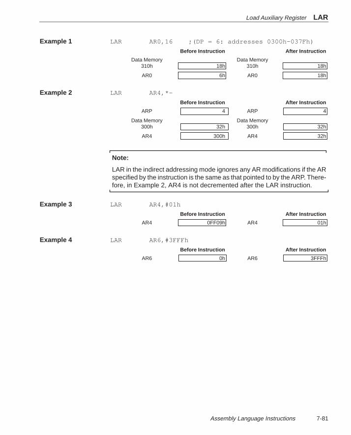
Load Auxiliary Register LAR
7-81 Assembly Language Instructions
Example 1 LAR AR0,16 ;(DP = 6: addresses 0300h–037Fh)
Before Instruction After Instruction
Data Memory Data Memory310h 18h 310h 18h
AR0 6h AR0 18h
Example 2 LAR AR4,*–
Before Instruction After Instruction
ARP 4 ARP 4
Data Memory Data Memory300h 32h 300h 32h
AR4 300h AR4 32h
Note:
LAR in the indirect addressing mode ignores any AR modifications if the ARspecified by the instruction is the same as that pointed to by the ARP. There-fore, in Example 2, AR4 is not decremented after the LAR instruction.
Example 3 LAR AR4,#01h
Before Instruction After Instruction
AR4 0FF09h AR4 01h
Example 4 LAR AR6,#3FFFh
Before Instruction After Instruction
AR6 0h AR6 3FFFh
LDP Load Data Page Pointer
7-82
Syntax LDP dma Direct addressingLDP ind [, ARn] Indirect addressingLDP #k Short immediate
addressing
Operands dma: 7 LSBs of the data-memory addressn: Value from 0 to 7 designating the next auxiliary registerk: 9-bit short immediate valueind: Select one of the following seven options:
* *+ *– *0+ *0– *BR0+ *BR0–
LDP dma15 14 13 12 11 10 9 8 7 6 5 4 3 2 1 0
0 0 0 0 1 1 0 1 0 dma
LDP ind [, ARn]15 14 13 12 11 10 9 8 7 6 5 4 3 2 1 0
0 0 0 0 1 1 0 1 1 ARU N NAR
Note: ARU, N, and NAR are defined in section 6.3, Indirect Addressing Mode (page 6-9).
LDP #k15 14 13 12 11 10 9 8 7 6 5 4 3 2 1 0
1 0 1 1 1 1 0 k
Execution Increment PC, then ...Event Addressing modeNine LSBs of (data-memory address) → DP Direct or indirect
k → DP Short immediate
Status Bits AffectsDP
Description The nine LSBs of the contents of the addressed data-memory location or a9-bit immediate value is loaded into the data page pointer (DP) of status regis-ter ST0. The DP can also be loaded by the LST instruction.
In direct addressing, the 9-bit DP and the 7-bit value specified in the instruction(dma) are concatenated to form the 16-bit data-memory address accessed bythe instruction. The DP provides the 9 MSBs, and dma provides the 7 LSBs.
Words 1
Opcode
Load Data Page Pointer LDP
7-83 Assembly Language Instructions
Cycles for a Single LDP Instruction (Using Direct and Indirect Addressing)
Program
Operand ROM DARAM SARAM External
DARAM 2 2 2 2+pcode
SARAM 2 2 2, 3† 2+pcode
External 2+dsrc 2+dsrc 2+dsrc 3+dsrc+pcode
† If the operand and the code are in the same SARAM block
Cycles for a Repeat (RPT) Execution of an LDP Instruction (Using Direct andIndirect Addressing)
Program
Operand ROM DARAM SARAM External
DARAM 2n 2n 2n 2n+pcode
SARAM 2n 2n 2n, 2n+1† 2n+pcode
External 2n+ndsrc 2n+ndsrc 2n+ndsrc 2n+1+ndsrcpcode
† If the operand and the code are in the same SARAM block
Cycles for a Single LDP Instruction (Using Short Immediate Addressing)
ROM DARAM SARAM External
2 2 2 2+pcode
Example 1 LDP 127 ;(DP = 511: addresses FF80h–FFFFh)
Before Instruction After Instruction
Data Memory Data MemoryFFFFh FEDCh FFFFh FEDCh
DP 1FFh DP 0DCh
Example 2 LDP #0h
Before Instruction After Instruction
DP 1FFh DP 0h
Example 3 LDP *,AR5
Before Instruction After Instruction
ARP 4 ARP 5
AR4 300h AR4 300h
Data Memory Data Memory300h 06h 300h 06h
DP 1FFh DP 06h
Cycles
LPH Load Product Register High Word
7-84
Syntax LPH dma Direct addressingLPH ind [, ARn] Indirect addressing
Operands dma: 7 LSBs of the data-memory addressn: Value from 0 to 7 designating the next auxiliary registerind: Select one of the following seven options:
* *+ *– *0+ *0– *BR0+ *BR0–
LPH dma15 14 13 12 11 10 9 8 7 6 5 4 3 2 1 0
0 1 1 1 0 1 0 1 0 dma
LPH ind [, ARn]15 14 13 12 11 10 9 8 7 6 5 4 3 2 1 0
0 1 1 1 0 1 0 1 1 ARU N NAR
Note: ARU, N, and NAR are defined in section 6.3, Indirect Addressing Mode (page 6-9).
Execution Increment PC, then ...(data-memory address) → PREG (31:16)
Status Bits None
Description The 16 high-order bits of the PREG are loaded with the content of the specifieddata-memory address. The low-order PREG bits are unaffected.
The LPH instruction can be used for restoring the high-order bits of the PREGafter interrupts and subroutine calls.
Words 1
Cycles for a Single LPH Instruction
Program
Operand ROM DARAM SARAM External
DARAM 1 1 1 1+p
SARAM 1 1 1, 2† 1+p
External 1+d 1+d 1+d 2+d+p
† If the operand and the code are in the same SARAM block
Opcode
Cycles
Load Product Register High Word LPH
7-85 Assembly Language Instructions
Cycles for a Repeat (RPT) Execution of an LPH Instruction
Program
Operand ROM DARAM SARAM External
DARAM n n n n+p
SARAM n n n, n+1† n+p
External n+nd n+nd n+nd n+1+p+nd
† If the operand and the code are in the same SARAM block
Example 1 LPH DAT0 ;(DP = 4)
Before Instruction After Instruction
Data Memory Data Memory200h 0F79Ch 200h 0F79Ch
PREG 30079844h PREG 0F79C9844h
Example 2 LPH *,AR6
Before Instruction After Instruction
ARP 5 ARP 6
AR5 200h AR5 200h
Data Memory Data Memory200h 0F79Ch 200h 0F79Ch
PREG 30079844h PREG 0F79C9844h
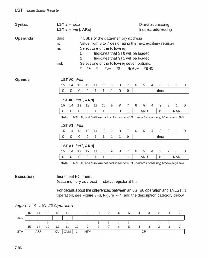
LST Load Status Register
7-86
Syntax LST #m, dma Direct addressingLST #m, ind [, ARn] Indirect addressing
Operands dma: 7 LSBs of the data-memory addressn: Value from 0 to 7 designating the next auxiliary registerm: Select one of the following:
0 Indicates that ST0 will be loaded1 Indicates that ST1 will be loaded
ind: Select one of the following seven options:* *+ *– *0+ *0– *BR0+ *BR0–
LST #0, dma15 14 13 12 11 10 9 8 7 6 5 4 3 2 1 0
0 0 0 0 1 1 1 0 0 dma
LST #0, ind [, ARn]15 14 13 12 11 10 9 8 7 6 5 4 3 2 1 0
0 0 0 0 1 1 1 0 1 ARU N NAR
Note: ARU, N, and NAR are defined in section 6.3, Indirect Addressing Mode (page 6-9).
LST #1, dma15 14 13 12 11 10 9 8 7 6 5 4 3 2 1 0
0 0 0 0 1 1 1 1 0 dma
LST #1, ind [, ARn]15 14 13 12 11 10 9 8 7 6 5 4 3 2 1 0
0 0 0 0 1 1 1 1 1 ARU N NAR
Note: ARU, N, and NAR are defined in section 6.3, Indirect Addressing Mode (page 6-9).
Execution Increment PC, then ...(data-memory address) → status register STm
For details about the differences between an LST #0 operation and an LST #1operation, see Figure 7–3, Figure 7–4, and the description category below.
Figure 7–3. LST #0 Operation
15 14 13 12 11 10 9 8 7 6 5 4 3 2 1 0
Data
↓ ↓ ↓ ↓ ↓ ↓ ↓ ↓ ↓ ↓ ↓ ↓ ↓ ↓15 14 13 12 11 10 9 8 7 6 5 4 3 2 1 0
ST0 ARP OV OVM 1 INTM DP
Opcode
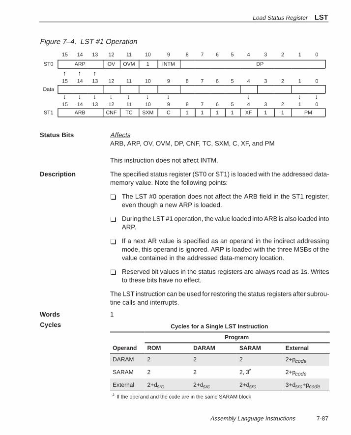
Load Status Register LST
7-87 Assembly Language Instructions
Figure 7–4. LST #1 Operation
15 14 13 12 11 10 9 8 7 6 5 4 3 2 1 0
ST0 ARP OV OVM 1 INTM DP
↑ ↑ ↑15 14 13 12 11 10 9 8 7 6 5 4 3 2 1 0
Data
↓ ↓ ↓ ↓ ↓ ↓ ↓ ↓ ↓ ↓15 14 13 12 11 10 9 8 7 6 5 4 3 2 1 0
ST1 ARB CNF TC SXM C 1 1 1 1 XF 1 1 PM
Status Bits Affects ARB, ARP, OV, OVM, DP, CNF, TC, SXM, C, XF, and PM
This instruction does not affect INTM.
Description The specified status register (ST0 or ST1) is loaded with the addressed data-memory value. Note the following points:
The LST #0 operation does not affect the ARB field in the ST1 register,even though a new ARP is loaded.
During the LST #1 operation, the value loaded into ARB is also loaded intoARP.
If a next AR value is specified as an operand in the indirect addressingmode, this operand is ignored. ARP is loaded with the three MSBs of thevalue contained in the addressed data-memory location.
Reserved bit values in the status registers are always read as 1s. Writesto these bits have no effect.
The LST instruction can be used for restoring the status registers after subrou-tine calls and interrupts.
Words 1
Cycles for a Single LST Instruction
Program
Operand ROM DARAM SARAM External
DARAM 2 2 2 2+pcode
SARAM 2 2 2, 3† 2+pcode
External 2+dsrc 2+dsrc 2+dsrc 3+dsrc+pcode
† If the operand and the code are in the same SARAM block
Cycles
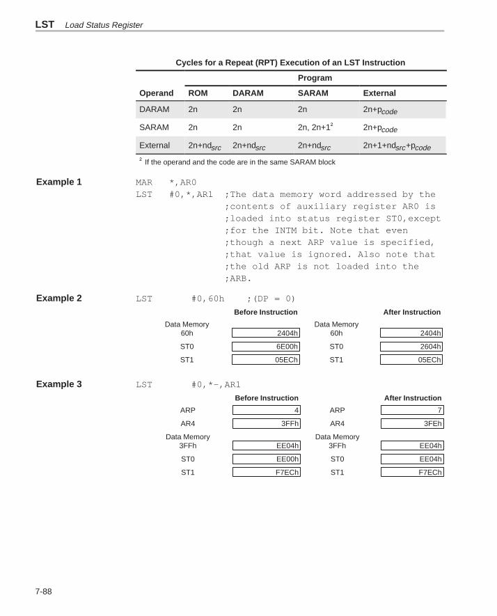
LST Load Status Register
7-88
Cycles for a Repeat (RPT) Execution of an LST Instruction
Program
Operand ROM DARAM SARAM External
DARAM 2n 2n 2n 2n+pcode
SARAM 2n 2n 2n, 2n+1† 2n+pcode
External 2n+ndsrc 2n+ndsrc 2n+ndsrc 2n+1+ndsrc+pcode
† If the operand and the code are in the same SARAM block
Example 1 MAR *,AR0LST #0,*,AR1 ;The data memory word addressed by the
;contents of auxiliary register AR0 is;loaded into status register ST0,except;for the INTM bit. Note that even;though a next ARP value is specified,;that value is ignored. Also note that;the old ARP is not loaded into the;ARB.
Example 2 LST #0,60h ;(DP = 0)
Before Instruction After Instruction
Data Memory Data Memory60h 2404h 60h 2404h
ST0 6E00h ST0 2604h
ST1 05ECh ST1 05ECh
Example 3 LST #0,*–,AR1
Before Instruction After Instruction
ARP 4 ARP 7
AR4 3FFh AR4 3FEh
Data Memory Data Memory3FFh EE04h 3FFh EE04h
ST0 EE00h ST0 EE04h
ST1 F7ECh ST1 F7ECh
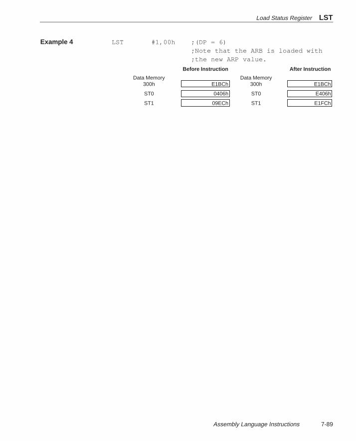
Load Status Register LST
7-89 Assembly Language Instructions
Example 4 LST #1,00h ;(DP = 6);Note that the ARB is loaded with;the new ARP value.
Before Instruction After Instruction
Data Memory Data Memory300h E1BCh 300h E1BCh
ST0 0406h ST0 E406h
ST1 09ECh ST1 E1FCh
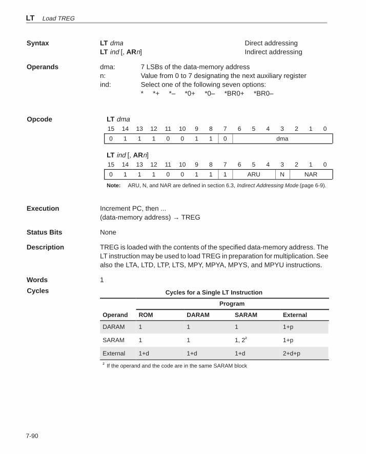
LT Load TREG
7-90
Syntax LT dma Direct addressingLT ind [, ARn] Indirect addressing
Operands dma: 7 LSBs of the data-memory addressn: Value from 0 to 7 designating the next auxiliary registerind: Select one of the following seven options:
* *+ *– *0+ *0– *BR0+ *BR0–
LT dma15 14 13 12 11 10 9 8 7 6 5 4 3 2 1 0
0 1 1 1 0 0 1 1 0 dma
LT ind [, ARn]15 14 13 12 11 10 9 8 7 6 5 4 3 2 1 0
0 1 1 1 0 0 1 1 1 ARU N NAR
Note: ARU, N, and NAR are defined in section 6.3, Indirect Addressing Mode (page 6-9).
Execution Increment PC, then ...(data-memory address) → TREG
Status Bits None
Description TREG is loaded with the contents of the specified data-memory address. TheLT instruction may be used to load TREG in preparation for multiplication. Seealso the LTA, LTD, LTP, LTS, MPY, MPYA, MPYS, and MPYU instructions.
Words 1
Cycles for a Single LT Instruction
Program
Operand ROM DARAM SARAM External
DARAM 1 1 1 1+p
SARAM 1 1 1, 2† 1+p
External 1+d 1+d 1+d 2+d+p
† If the operand and the code are in the same SARAM block
Opcode
Cycles
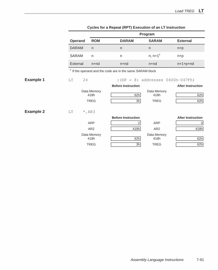
Load TREG LT
7-91 Assembly Language Instructions
Cycles for a Repeat (RPT) Execution of an LT Instruction
Program
Operand ROM DARAM SARAM External
DARAM n n n n+p
SARAM n n n, n+1† n+p
External n+nd n+nd n+nd n+1+p+nd
† If the operand and the code are in the same SARAM block
Example 1 LT 24 ;(DP = 8: addresses 0400h–047Fh)
Before Instruction After Instruction
Data Memory Data Memory418h 62h 418h 62h
TREG 3h TREG 62h
Example 2 LT *,AR3
Before Instruction After Instruction
ARP 2 ARP 3
AR2 418h AR2 418h
Data Memory Data Memory418h 62h 418h 62h
TREG 3h TREG 62h
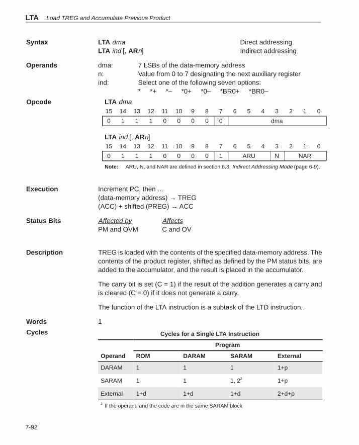
LTA Load TREG and Accumulate Previous Product
7-92
Syntax LTA dma Direct addressingLTA ind [, ARn] Indirect addressing
Operands dma: 7 LSBs of the data-memory addressn: Value from 0 to 7 designating the next auxiliary registerind: Select one of the following seven options:
* *+ *– *0+ *0– *BR0+ *BR0–
LTA dma15 14 13 12 11 10 9 8 7 6 5 4 3 2 1 0
0 1 1 1 0 0 0 0 0 dma
LTA ind [, ARn]15 14 13 12 11 10 9 8 7 6 5 4 3 2 1 0
0 1 1 1 0 0 0 0 1 ARU N NAR
Note: ARU, N, and NAR are defined in section 6.3, Indirect Addressing Mode (page 6-9).
Execution Increment PC, then ...(data-memory address) → TREG(ACC) + shifted (PREG) → ACC
Status Bits Affected by AffectsPM and OVM C and OV
Description TREG is loaded with the contents of the specified data-memory address. Thecontents of the product register, shifted as defined by the PM status bits, areadded to the accumulator, and the result is placed in the accumulator.
The carry bit is set (C = 1) if the result of the addition generates a carry andis cleared (C = 0) if it does not generate a carry.
The function of the LTA instruction is a subtask of the LTD instruction.
Words 1
Cycles for a Single LTA Instruction
Program
Operand ROM DARAM SARAM External
DARAM 1 1 1 1+p
SARAM 1 1 1, 2† 1+p
External 1+d 1+d 1+d 2+d+p
† If the operand and the code are in the same SARAM block
Opcode
Cycles
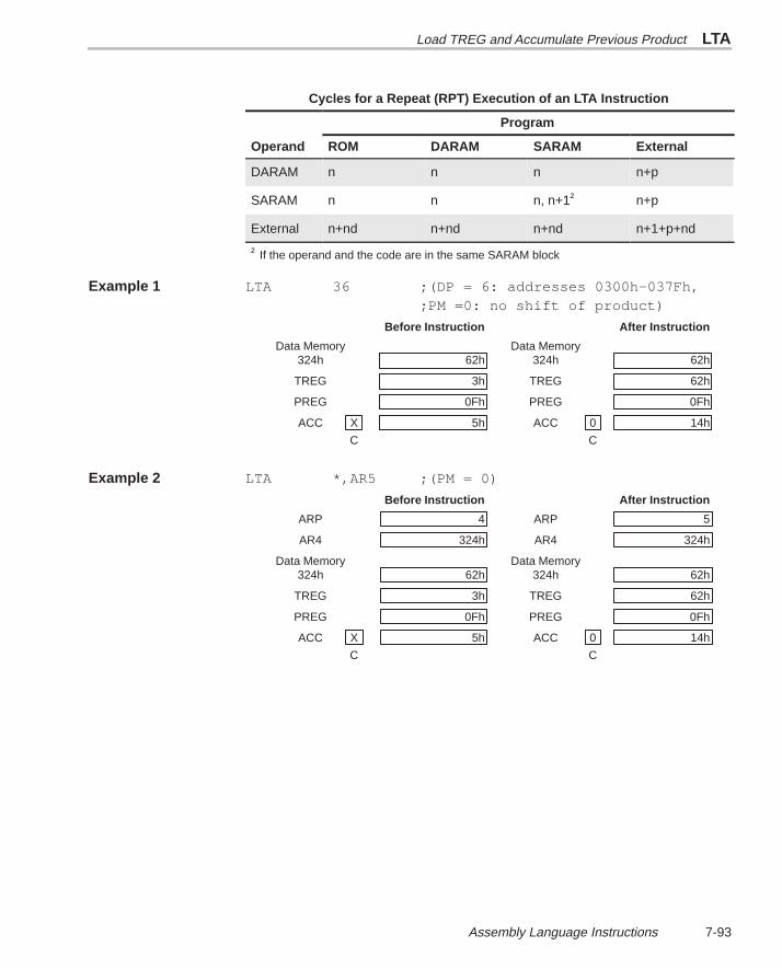
Load TREG and Accumulate Previous Product LTA
7-93 Assembly Language Instructions
Cycles for a Repeat (RPT) Execution of an LTA Instruction
Program
Operand ROM DARAM SARAM External
DARAM n n n n+p
SARAM n n n, n+1† n+p
External n+nd n+nd n+nd n+1+p+nd
† If the operand and the code are in the same SARAM block
Example 1 LTA 36 ;(DP = 6: addresses 0300h–037Fh,;PM =0: no shift of product)
Before Instruction After Instruction
Data Memory Data Memory324h 62h 324h 62h
TREG 3h TREG 62h
PREG 0Fh PREG 0Fh
ACC X 5h ACC 0 14h
C C
Example 2 LTA *,AR5 ;(PM = 0)
Before Instruction After Instruction
ARP 4 ARP 5
AR4 324h AR4 324h
Data Memory Data Memory324h 62h 324h 62h
TREG 3h TREG 62h
PREG 0Fh PREG 0Fh
ACC X 5h ACC 0 14h
C C
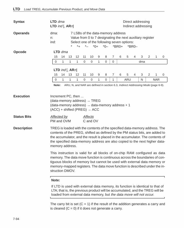
LTD Load TREG, Accumulate Previous Product, and Move Data
7-94
Syntax LTD dma Direct addressingLTD ind [, ARn] Indirect addressing
Operands dma: 7 LSBs of the data-memory addressn: Value from 0 to 7 designating the next auxiliary registerind: Select one of the following seven options:
* *+ *– *0+ *0– *BR0+ *BR0–
LTD dma15 14 13 12 11 10 9 8 7 6 5 4 3 2 1 0
0 1 1 1 0 0 1 0 0 dma
LTD ind [, ARn]15 14 13 12 11 10 9 8 7 6 5 4 3 2 1 0
0 1 1 1 0 0 1 0 1 ARU N NAR
Note: ARU, N, and NAR are defined in section 6.3, Indirect Addressing Mode (page 6-9).
Execution Increment PC, then ...(data-memory address) → TREG(data-memory address) → data-memory address + 1 (ACC) + shifted (PREG) → ACC
Status Bits Affected by AffectsPM and OVM C and OV
Description TREG is loaded with the contents of the specified data-memory address. Thecontents of the PREG, shifted as defined by the PM status bits, are added tothe accumulator, and the result is placed in the accumulator. The contents ofthe specified data-memory address are also copied to the next higher data-memory address.
This instruction is valid for all blocks of on-chip RAM configured as datamemory. The data move function is continuous across the boundaries of con-tiguous blocks of memory but cannot be used with external data memory ormemory-mapped registers. The data move function is described under the in-struction DMOV.
Note:
If LTD is used with external data memory, its function is identical to that ofLTA; that is, the previous product will be accumulated, and the TREG will beloaded from external data memory, but the data move will not occur.
The carry bit is set (C = 1) if the result of the addition generates a carry andis cleared (C = 0) if it does not generate a carry.
Opcode
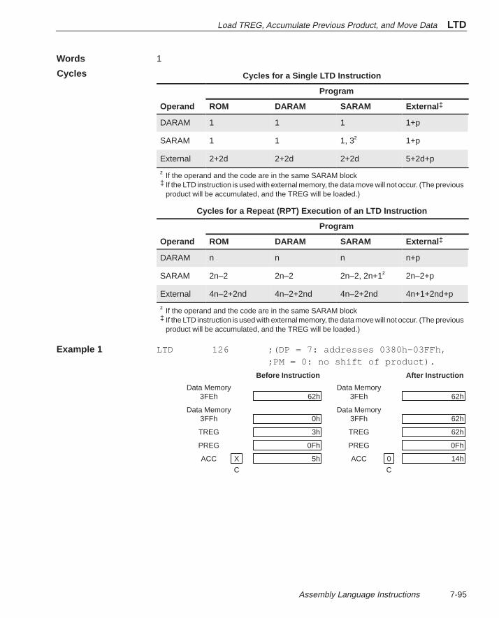
Load TREG, Accumulate Previous Product, and Move Data LTD
7-95 Assembly Language Instructions
Words 1
Cycles for a Single LTD Instruction
Program
Operand ROM DARAM SARAM External ‡
DARAM 1 1 1 1+p
SARAM 1 1 1, 3† 1+p
External 2+2d 2+2d 2+2d 5+2d+p
† If the operand and the code are in the same SARAM block‡ If the LTD instruction is used with external memory, the data move will not occur. (The previous
product will be accumulated, and the TREG will be loaded.)
Cycles for a Repeat (RPT) Execution of an LTD Instruction
Program
Operand ROM DARAM SARAM External ‡
DARAM n n n n+p
SARAM 2n–2 2n–2 2n–2, 2n+1† 2n–2+p
External 4n–2+2nd 4n–2+2nd 4n–2+2nd 4n+1+2nd+p
† If the operand and the code are in the same SARAM block‡ If the LTD instruction is used with external memory, the data move will not occur. (The previous
product will be accumulated, and the TREG will be loaded.)
Example 1 LTD 126 ;(DP = 7: addresses 0380h–03FFh,;PM = 0: no shift of product).
Before Instruction After Instruction
Data Memory Data Memory3FEh 62h 3FEh 62h
Data Memory Data Memory3FFh 0h 3FFh 62h
TREG 3h TREG 62h
PREG 0Fh PREG 0Fh
ACC X 5h ACC 0 14h
C C
Cycles
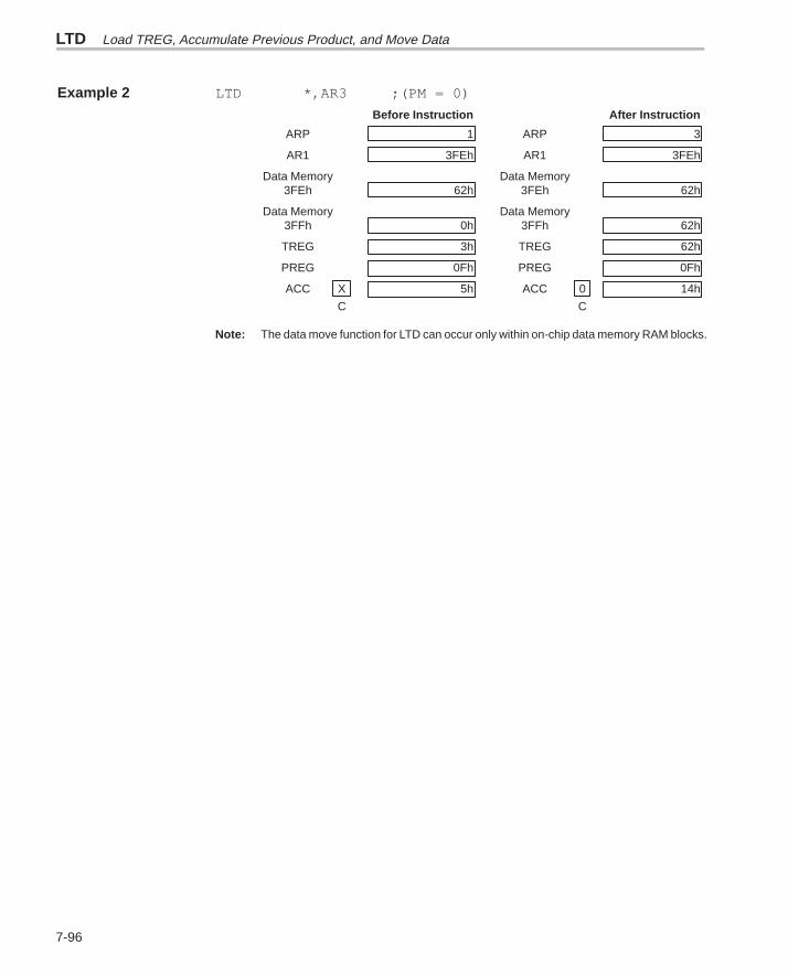
LTD Load TREG, Accumulate Previous Product, and Move Data
7-96
Example 2 LTD *,AR3 ;(PM = 0)
Before Instruction After Instruction
ARP 1 ARP 3
AR1 3FEh AR1 3FEh
Data Memory Data Memory3FEh 62h 3FEh 62h
Data Memory Data Memory3FFh 0h 3FFh 62h
TREG 3h TREG 62h
PREG 0Fh PREG 0Fh
ACC X 5h ACC 0 14h
C C
Note: The data move function for LTD can occur only within on-chip data memory RAM blocks.
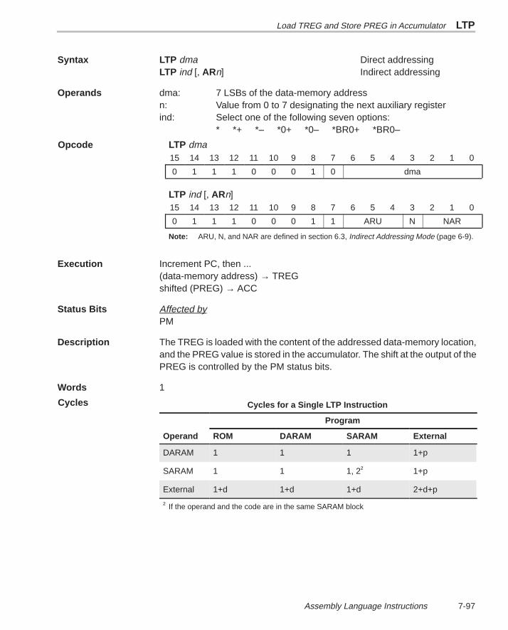
Load TREG and Store PREG in Accumulator LTP
7-97 Assembly Language Instructions
Syntax LTP dma Direct addressingLTP ind [, ARn] Indirect addressing
Operands dma: 7 LSBs of the data-memory addressn: Value from 0 to 7 designating the next auxiliary registerind: Select one of the following seven options:
* *+ *– *0+ *0– *BR0+ *BR0–
LTP dma15 14 13 12 11 10 9 8 7 6 5 4 3 2 1 0
0 1 1 1 0 0 0 1 0 dma
LTP ind [, ARn]15 14 13 12 11 10 9 8 7 6 5 4 3 2 1 0
0 1 1 1 0 0 0 1 1 ARU N NAR
Note: ARU, N, and NAR are defined in section 6.3, Indirect Addressing Mode (page 6-9).
Execution Increment PC, then ...(data-memory address) → TREGshifted (PREG) → ACC
Status Bits Affected byPM
Description The TREG is loaded with the content of the addressed data-memory location,and the PREG value is stored in the accumulator. The shift at the output of thePREG is controlled by the PM status bits.
Words 1
Cycles for a Single LTP Instruction
Program
Operand ROM DARAM SARAM External
DARAM 1 1 1 1+p
SARAM 1 1 1, 2† 1+p
External 1+d 1+d 1+d 2+d+p
† If the operand and the code are in the same SARAM block
Opcode
Cycles
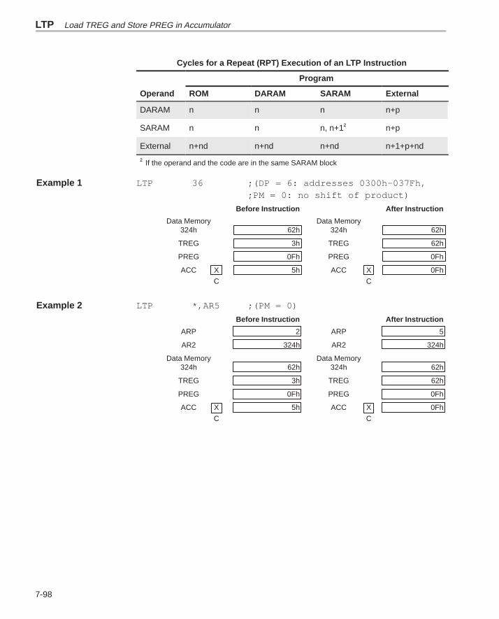
LTP Load TREG and Store PREG in Accumulator
7-98
Cycles for a Repeat (RPT) Execution of an LTP Instruction
Program
Operand ROM DARAM SARAM External
DARAM n n n n+p
SARAM n n n, n+1† n+p
External n+nd n+nd n+nd n+1+p+nd
† If the operand and the code are in the same SARAM block
Example 1 LTP 36 ;(DP = 6: addresses 0300h–037Fh,;PM = 0: no shift of product)
Before Instruction After Instruction
Data Memory Data Memory324h 62h 324h 62h
TREG 3h TREG 62h
PREG 0Fh PREG 0Fh
ACC X 5h ACC X 0Fh
C C
Example 2 LTP *,AR5 ;(PM = 0)
Before Instruction After Instruction
ARP 2 ARP 5
AR2 324h AR2 324h
Data Memory Data Memory324h 62h 324h 62h
TREG 3h TREG 62h
PREG 0Fh PREG 0Fh
ACC X 5h ACC X 0Fh
C C
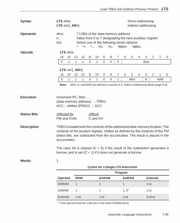
Load TREG and Subtract Previous Product LTS
7-99 Assembly Language Instructions
Syntax LTS dma Direct addressingLTS ind [, ARn] Indirect addressing
Operands dma: 7 LSBs of the data-memory addressn: Value from 0 to 7 designating the next auxiliary registerind: Select one of the following seven options:
* *+ *– *0+ *0– *BR0+ *BR0–
LTS dma15 14 13 12 11 10 9 8 7 6 5 4 3 2 1 0
0 1 1 1 0 1 0 0 0 dma
LTS ind [, ARn]15 14 13 12 11 10 9 8 7 6 5 4 3 2 1 0
0 1 1 1 0 1 0 0 1 ARU N NAR
Note: ARU, N, and NAR are defined in section 6.3, Indirect Addressing Mode (page 6-9).
Execution Increment PC, then ...(data-memory address) → TREGACC – shifted (PREG) → ACC
Status Bits Affected by AffectsPM and OVM C and OV
Description TREG is loaded with the contents of the addressed data-memory location. Thecontents of the product register, shifted as defined by the contents of the PMstatus bits, are subtracted from the accumulator. The result is placed in theaccumulator.
The carry bit is cleared (C = 0) if the result of the subtraction generates aborrow, and is set (C = 1) if it does not generate a borrow.
Words 1
Cycles for a Single LTS Instruction
Program
Operand ROM DARAM SARAM External
DARAM 1 1 1 1+p
SARAM 1 1 1, 2† 1+p
External 1+d 1+d 1+d 2+d+p
† If the operand and the code are in the same SARAM block
Opcode
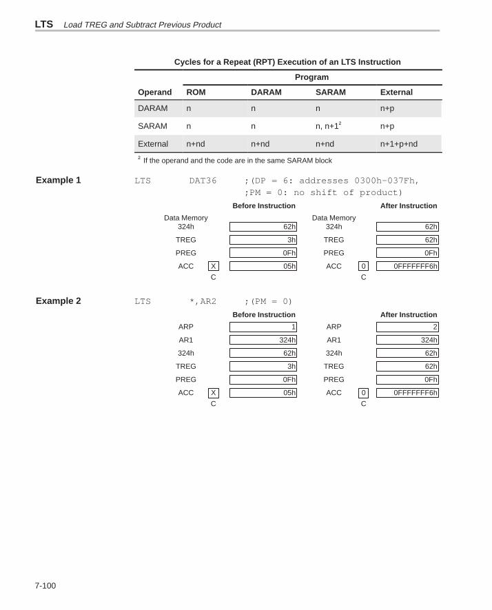
LTS Load TREG and Subtract Previous Product
7-100
Cycles for a Repeat (RPT) Execution of an LTS Instruction
Program
Operand ROM DARAM SARAM External
DARAM n n n n+p
SARAM n n n, n+1† n+p
External n+nd n+nd n+nd n+1+p+nd
† If the operand and the code are in the same SARAM block
Example 1 LTS DAT36 ;(DP = 6: addresses 0300h–037Fh,;PM = 0: no shift of product)
Before Instruction After Instruction
Data Memory Data Memory324h 62h 324h 62h
TREG 3h TREG 62h
PREG 0Fh PREG 0Fh
ACC X 05h ACC 0 0FFFFFFF6h
C C
Example 2 LTS *,AR2 ;(PM = 0)
Before Instruction After Instruction
ARP 1 ARP 2
AR1 324h AR1 324h
324h 62h 324h 62h
TREG 3h TREG 62h
PREG 0Fh PREG 0Fh
ACC X 05h ACC 0 0FFFFFFF6h
C C
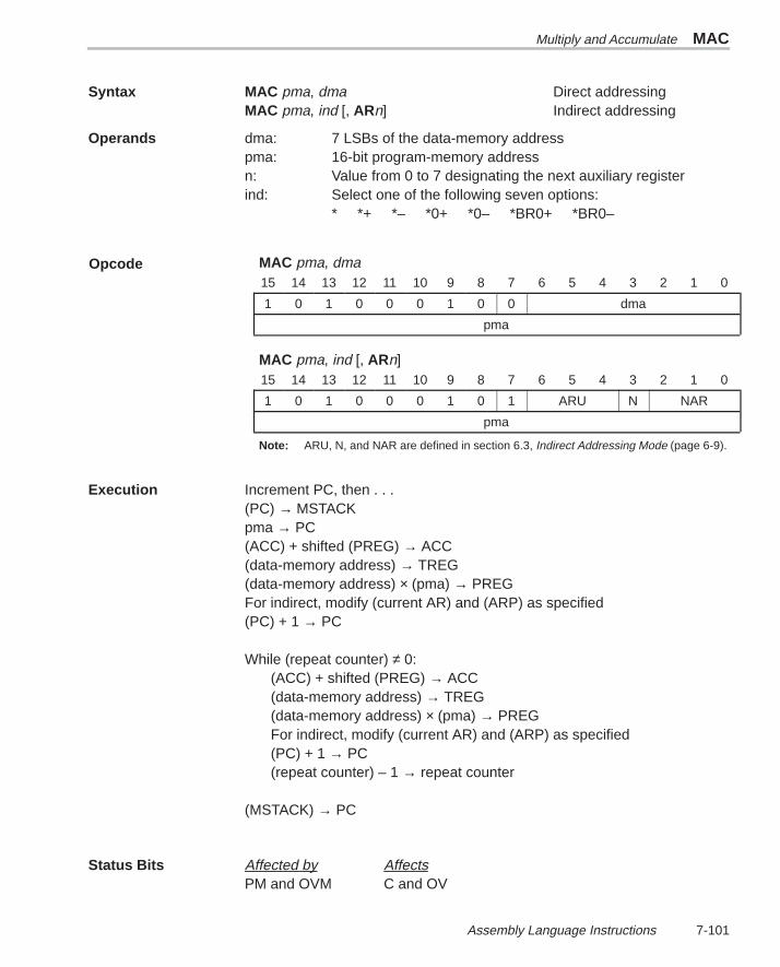
Multiply and Accumulate MAC
7-101 Assembly Language Instructions
Syntax MAC pma, dma Direct addressingMAC pma, ind [, ARn] Indirect addressing
Operands dma: 7 LSBs of the data-memory addresspma: 16-bit program-memory addressn: Value from 0 to 7 designating the next auxiliary registerind: Select one of the following seven options:
* *+ *– *0+ *0– *BR0+ *BR0–
MAC pma, dma15 14 13 12 11 10 9 8 7 6 5 4 3 2 1 0
1 0 1 0 0 0 1 0 0 dma
pma
MAC pma, ind [, ARn]15 14 13 12 11 10 9 8 7 6 5 4 3 2 1 0
1 0 1 0 0 0 1 0 1 ARU N NAR
pma
Note: ARU, N, and NAR are defined in section 6.3, Indirect Addressing Mode (page 6-9).
Execution Increment PC, then . . .(PC) → MSTACKpma → PC(ACC) + shifted (PREG) → ACC(data-memory address) → TREG(data-memory address) × (pma) → PREGFor indirect, modify (current AR) and (ARP) as specified(PC) + 1 → PC
While (repeat counter) ≠ 0:(ACC) + shifted (PREG) → ACC(data-memory address) → TREG(data-memory address) × (pma) → PREGFor indirect, modify (current AR) and (ARP) as specified(PC) + 1 → PC(repeat counter) – 1 → repeat counter
(MSTACK) → PC
Status Bits Affected by AffectsPM and OVM C and OV
Opcode
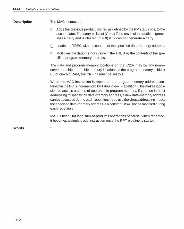
MAC Multiply and Accumulate
7-102
Description The MAC instruction:
Adds the previous product, shifted as defined by the PM status bits, to theaccumulator. The carry bit is set (C = 1) if the result of the addition gener-ates a carry and is cleared (C = 0) if it does not generate a carry.
Loads the TREG with the content of the specified data-memory address.
Multiplies the data-memory value in the TREG by the contents of the spe-cified program-memory address.
The data and program memory locations on the ’C20x may be any nonre-served on-chip or off-chip memory locations. If the program memory is blockB0 of on-chip RAM, the CNF bit must be set to 1.
When the MAC instruction is repeated, the program-memory address con-tained in the PC is incremented by 1 during each repetition. This makes it pos-sible to access a series of operands in program memory. If you use indirectaddressing to specify the data-memory address, a new data-memory addresscan be accessed during each repetition. If you use the direct addressing mode,the specified data-memory address is a constant; it will not be modified duringeach repetition.
MAC is useful for long sum-of-products operations because, when repeated,it becomes a single-cycle instruction once the RPT pipeline is started.
Words 2
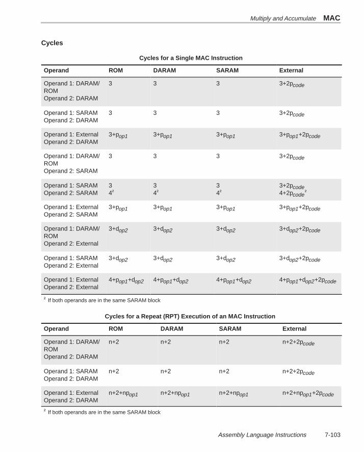
Multiply and Accumulate MAC
7-103 Assembly Language Instructions
Cycles
Cycles for a Single MAC Instruction
Operand ROM DARAM SARAM External
Operand 1: DARAM/ROMOperand 2: DARAM
3 3 3 3+2pcode
Operand 1: SARAMOperand 2: DARAM
3 3 3 3+2pcode
Operand 1: ExternalOperand 2: DARAM
3+pop1 3+pop1 3+pop1 3+pop1+2pcode
Operand 1: DARAM/ROMOperand 2: SARAM
3 3 3 3+2pcode
Operand 1: SARAMOperand 2: SARAM
34†
34†
34†
3+2pcode4+2pcode†
Operand 1: ExternalOperand 2: SARAM
3+pop1 3+pop1 3+pop1 3+pop1+2pcode
Operand 1: DARAM/ROMOperand 2: External
3+dop2 3+dop2 3+dop2 3+dop2+2pcode
Operand 1: SARAMOperand 2: External
3+dop2 3+dop2 3+dop2 3+dop2+2pcode
Operand 1: ExternalOperand 2: External
4+pop1+dop2 4+pop1+dop2 4+pop1+dop2 4+pop1+dop2+2pcode
† If both operands are in the same SARAM block
Cycles for a Repeat (RPT) Execution of an MAC Instruction
Operand ROM DARAM SARAM External
Operand 1: DARAM/ROMOperand 2: DARAM
n+2 n+2 n+2 n+2+2pcode
Operand 1: SARAMOperand 2: DARAM
n+2 n+2 n+2 n+2+2pcode
Operand 1: ExternalOperand 2: DARAM
n+2+npop1 n+2+npop1 n+2+npop1 n+2+npop1+2pcode
† If both operands are in the same SARAM block
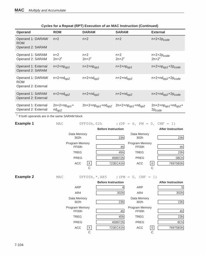
MAC Multiply and Accumulate
7-104
Cycles for a Repeat (RPT) Execution of an MAC Instruction (Continued)
Operand ExternalSARAMDARAMROM
Operand 1: DARAM/ROMOperand 2: SARAM
n+2 n+2 n+2 n+2+2pcode
Operand 1: SARAMOperand 2: SARAM
n+22n+2†
n+22n+2†
n+22n+2†
n+2+2pcode2n+2†
Operand 1: ExternalOperand 2: SARAM
n+2+npop1 n+2+npop1 n+2+npop1 n+2+npop1+2pcode
Operand 1: DARAM/ROMOperand 2: External
n+2+ndop2 n+2+ndop2 n+2+ndop2 n+2+ndop2+2pcode
Operand 1: SARAMOperand 2: External
n+2+ndop2 n+2+ndop2 n+2+ndop2 n+2+ndop2+2pcode
Operand 1: ExternalOperand 2: External
2n+2+npop1+ndop2
2n+2+npop1+ndop2 2n+2+npop1+ndop2 2n+2+npop1+ndop2+2pcode
† If both operands are in the same SARAM block
Example 1 MAC 0FF00h,02h ;(DP = 6, PM = 0, CNF = 1)
Before Instruction After Instruction
Data Memory Data Memory302h 23h 302h 23h
Program Memory Program MemoryFF00h 4h FF00h 4h
TREG 45h TREG 23h
PREG 458972h PREG 08Ch
ACC X 723EC41h ACC 0 76975B3h
C C
Example 2 MAC 0FF00h,*,AR5 ;(PM = 0, CNF = 1)
Before Instruction After Instruction
ARP 4 ARP 5
AR4 302h AR4 302h
Data Memory Data Memory302h 23h 302h 23h
Program Memory Program MemoryFF00h 4h FF00h 4h
TREG 45h TREG 23h
PREG 458972h PREG 8Ch
ACC X 723EC41h ACC 0 76975B3h
C C
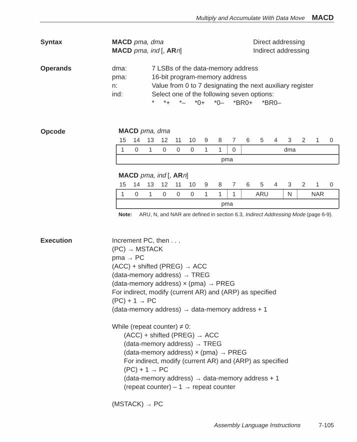
Multiply and Accumulate With Data Move MACD
7-105 Assembly Language Instructions
Syntax MACD pma, dma Direct addressingMACD pma, ind [, ARn] Indirect addressing
Operands dma: 7 LSBs of the data-memory addresspma: 16-bit program-memory addressn: Value from 0 to 7 designating the next auxiliary registerind: Select one of the following seven options:
* *+ *– *0+ *0– *BR0+ *BR0–
MACD pma, dma15 14 13 12 11 10 9 8 7 6 5 4 3 2 1 0
1 0 1 0 0 0 1 1 0 dma
pma
MACD pma, ind [, ARn]15 14 13 12 11 10 9 8 7 6 5 4 3 2 1 0
1 0 1 0 0 0 1 1 1 ARU N NAR
pma
Note: ARU, N, and NAR are defined in section 6.3, Indirect Addressing Mode (page 6-9).
Execution Increment PC, then . . .(PC) → MSTACKpma → PC(ACC) + shifted (PREG) → ACC(data-memory address) → TREG(data-memory address) × (pma) → PREGFor indirect, modify (current AR) and (ARP) as specified(PC) + 1 → PC(data-memory address) → data-memory address + 1
While (repeat counter) ≠ 0:(ACC) + shifted (PREG) → ACC(data-memory address) → TREG(data-memory address) × (pma) → PREGFor indirect, modify (current AR) and (ARP) as specified(PC) + 1 → PC(data-memory address) → data-memory address + 1(repeat counter) – 1 → repeat counter
(MSTACK) → PC
Opcode
MACD Multiply and Accumulate With Data Move
7-106
Status Bits Affected by AffectsPM and OVM C and OV
Description The MACD instruction:
Adds the previous product, shifted as defined by the PM status bits, to theaccumulator. The carry bit is set (C = 1) if the result of the addition gener-ates a carry and is cleared (C = 0) if it does not generate a carry.
Loads the TREG with the content of the specified data-memory address.
Multiplies the data-memory value in the TREG by the contents of the spe-cified program-memory address.
Copies the contents of the specified data-memory address to the nexthigher data-memory address.
The data- and program-memory locations on the ’C20x may be any nonre-served, on-chip or off-chip memory locations. If the program memory is blockB0 of on-chip RAM, the CNF bit must be set to 1. If MACD addresses one ofthe memory-mapped registers or external memory as a data-memory location,the effect of the instruction is that of a MAC instruction; the data move will notoccur (see the DMOV instruction description).
When the MACD instruction is repeated, the program-memory address con-tained in the PC is incremented by 1 during each repetition. This makes it pos-sible to access a series of operands in program memory. If you use indirectaddressing to specify the data-memory address, a new data-memory addresscan be accessed during each repetition. If you use the direct addressing mode,the specified data-memory address is a constant; it will not be modified duringeach repetition.
MACD functions in the same manner as MAC, with the addition of a data movefor on-chip RAM blocks. This feature makes MACD useful for applicationssuch as convolution and transversal filtering. When used with RPT, MACD be-comes a single-cycle instruction once the RPT pipeline is started.
Words 2
Cycles
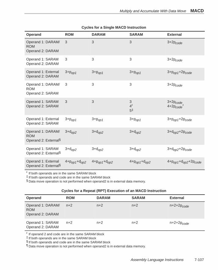
Multiply and Accumulate With Data Move MACD
7-107 Assembly Language Instructions
Cycles for a Single MACD Instruction
Operand ROM DARAM SARAM External
Operand 1: DARAM/ROMOperand 2: DARAM
3 3 3 3+2pcode
Operand 1: SARAMOperand 2: DARAM
3 3 3 3+2pcode
Operand 1: ExternalOperand 2: DARAM
3+pop1 3+pop1 3+pop1 3+pop1+2pcode
Operand 1: DARAM/ROMOperand 2: SARAM
3 3 3 3+2pcode
Operand 1: SARAMOperand 2: SARAM
3 3 34†
5‡
3+2pcode4+2pcode†
Operand 1: ExternalOperand 2: SARAM
3+pop1 3+pop1 3+pop1 3+pop1+2pcode
Operand 1: DARAM/ROMOperand 2: External§
3+dop2 3+dop2 3+dop2 3+dop2+2pcode
Operand 1: SARAMOperand 2: External§
3+dop2 3+dop2 3+dop2 3+dop2+2pcode
Operand 1: ExternalOperand 2: External§
4+pop1+dop2 4+pop1+dop2 4+pop1+dop2 4+pop1+dop2+2pcode
† If both operands are in the same SARAM block‡ If both operands and code are in the same SARAM block§ Data move operation is not performed when operand2 is in external data memory.
Cycles for a Repeat (RPT) Execution of an MACD Instruction
Operand ROM DARAM SARAM External
Operand 1: DARAM/ROMOperand 2: DARAM
n+2 n+2 n+2 n+2+2pcode
Operand 1: SARAMOperand 2: DARAM
n+2 n+2 n+2 n+2+2pcode
† If operand 2 and code are in the same SARAM block‡ If both operands are in the same SARAM block§ If both operands and code are in the same SARAM block¶ Data move operation is not performed when operand2 is in external data memory.
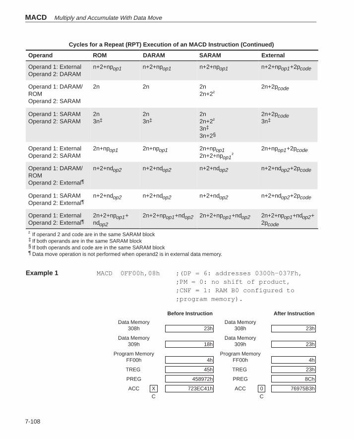
MACD Multiply and Accumulate With Data Move
7-108
Cycles for a Repeat (RPT) Execution of an MACD Instruction (Continued)
Operand ExternalSARAMDARAMROM
Operand 1: ExternalOperand 2: DARAM
n+2+npop1 n+2+npop1 n+2+npop1 n+2+npop1+2pcode
Operand 1: DARAM/ROMOperand 2: SARAM
2n 2n 2n2n+2†
2n+2pcode
Operand 1: SARAMOperand 2: SARAM
2n3n‡
2n3n‡
2n2n+2†
3n‡
3n+2§
2n+2pcode3n‡
Operand 1: ExternalOperand 2: SARAM
2n+npop1 2n+npop1 2n+npop12n+2+npop1†
2n+npop1+2pcode
Operand 1: DARAM/ROMOperand 2: External¶
n+2+ndop2 n+2+ndop2 n+2+ndop2 n+2+ndop2+2pcode
Operand 1: SARAMOperand 2: External¶
n+2+ndop2 n+2+ndop2 n+2+ndop2 n+2+ndop2+2pcode
Operand 1: ExternalOperand 2: External¶
2n+2+npop1+ndop2
2n+2+npop1+ndop2 2n+2+npop1+ndop2 2n+2+npop1+ndop2+2pcode
† If operand 2 and code are in the same SARAM block‡ If both operands are in the same SARAM block§ If both operands and code are in the same SARAM block¶ Data move operation is not performed when operand2 is in external data memory.
Example 1 MACD 0FF00h,08h ;(DP = 6: addresses 0300h–037Fh,;PM = 0: no shift of product,;CNF = 1: RAM B0 configured to;program memory).
Before Instruction After Instruction
Data Memory Data Memory308h 23h 308h 23h
Data Memory Data Memory309h 18h 309h 23h
Program Memory Program MemoryFF00h 4h FF00h 4h
TREG 45h TREG 23h
PREG 458972h PREG 8Ch
ACC X 723EC41h ACC 0 76975B3h
C C
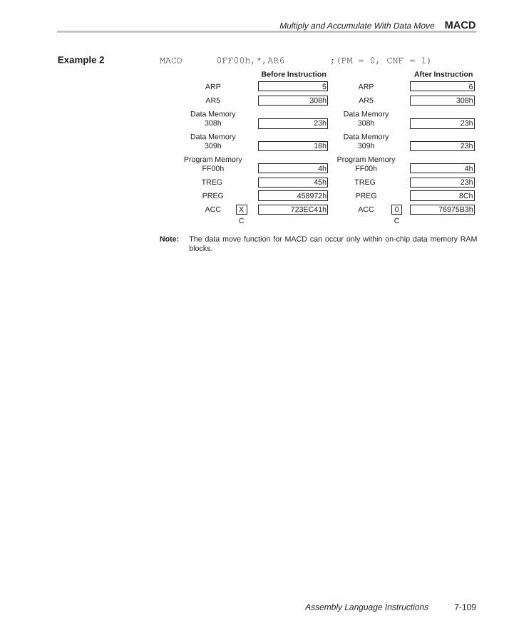
Multiply and Accumulate With Data Move MACD
7-109 Assembly Language Instructions
Example 2 MACD 0FF00h,*,AR6 ;(PM = 0, CNF = 1)
Before Instruction After Instruction
ARP 5 ARP 6
AR5 308h AR5 308h
Data Memory Data Memory308h 23h 308h 23h
Data Memory Data Memory309h 18h 309h 23h
Program Memory Program MemoryFF00h 4h FF00h 4h
TREG 45h TREG 23h
PREG 458972h PREG 8Ch
ACC X 723EC41h ACC 0 76975B3h
C C
Note: The data move function for MACD can occur only within on-chip data memory RAMblocks.
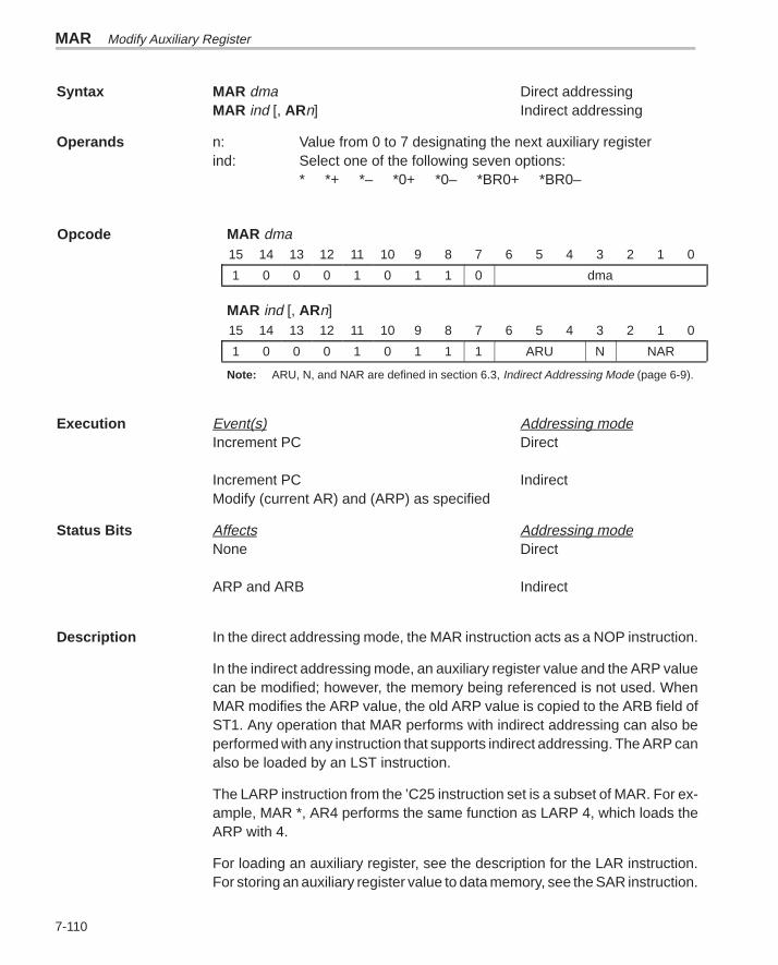
MAR Modify Auxiliary Register
7-110
Syntax MAR dma Direct addressingMAR ind [, ARn] Indirect addressing
Operands n: Value from 0 to 7 designating the next auxiliary registerind: Select one of the following seven options:
* *+ *– *0+ *0– *BR0+ *BR0–
MAR dma15 14 13 12 11 10 9 8 7 6 5 4 3 2 1 0
1 0 0 0 1 0 1 1 0 dma
MAR ind [, ARn]15 14 13 12 11 10 9 8 7 6 5 4 3 2 1 0
1 0 0 0 1 0 1 1 1 ARU N NAR
Note: ARU, N, and NAR are defined in section 6.3, Indirect Addressing Mode (page 6-9).
Execution Event(s) Addressing modeIncrement PC Direct
Increment PC IndirectModify (current AR) and (ARP) as specified
Status Bits Affects Addressing modeNone Direct
ARP and ARB Indirect
Description In the direct addressing mode, the MAR instruction acts as a NOP instruction.
In the indirect addressing mode, an auxiliary register value and the ARP valuecan be modified; however, the memory being referenced is not used. WhenMAR modifies the ARP value, the old ARP value is copied to the ARB field ofST1. Any operation that MAR performs with indirect addressing can also beperformed with any instruction that supports indirect addressing. The ARP canalso be loaded by an LST instruction.
The LARP instruction from the ’C25 instruction set is a subset of MAR. For ex-ample, MAR *, AR4 performs the same function as LARP 4, which loads theARP with 4.
For loading an auxiliary register, see the description for the LAR instruction.For storing an auxiliary register value to data memory, see the SAR instruction.
Opcode
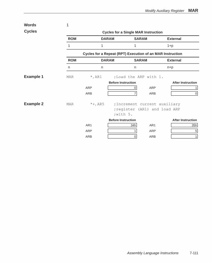
Modify Auxiliary Register MAR
7-111 Assembly Language Instructions
Words 1
Cycles for a Single MAR Instruction
ROM DARAM SARAM External
1 1 1 1+p
Cycles for a Repeat (RPT) Execution of an MAR Instruction
ROM DARAM SARAM External
n n n n+p
Example 1 MAR *,AR1 ;Load the ARP with 1.
Before Instruction After Instruction
ARP 0 ARP 1
ARB 7 ARB 0
Example 2 MAR *+,AR5 ;Increment current auxiliary;register (AR1) and load ARP;with 5.
Before Instruction After Instruction
AR1 34h AR1 35h
ARP 1 ARP 5
ARB 0 ARB 1
Cycles
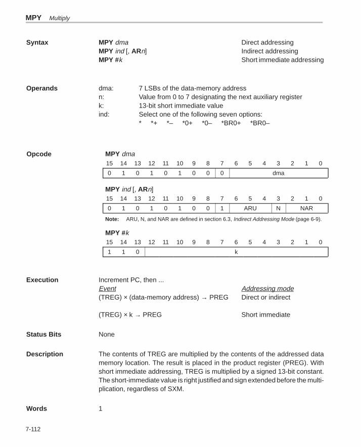
MPY Multiply
7-112
Syntax MPY dma Direct addressingMPY ind [, ARn] Indirect addressingMPY #k Short immediate addressing
Operands dma: 7 LSBs of the data-memory addressn: Value from 0 to 7 designating the next auxiliary registerk: 13-bit short immediate valueind: Select one of the following seven options:
* *+ *– *0+ *0– *BR0+ *BR0–
MPY dma15 14 13 12 11 10 9 8 7 6 5 4 3 2 1 0
0 1 0 1 0 1 0 0 0 dma
MPY ind [, ARn]15 14 13 12 11 10 9 8 7 6 5 4 3 2 1 0
0 1 0 1 0 1 0 0 1 ARU N NAR
Note: ARU, N, and NAR are defined in section 6.3, Indirect Addressing Mode (page 6-9).
MPY #k15 14 13 12 11 10 9 8 7 6 5 4 3 2 1 0
1 1 0 k
Execution Increment PC, then ...Event Addressing mode(TREG) × (data-memory address) → PREG Direct or indirect
(TREG) × k → PREG Short immediate
Status Bits None
Description The contents of TREG are multiplied by the contents of the addressed datamemory location. The result is placed in the product register (PREG). Withshort immediate addressing, TREG is multiplied by a signed 13-bit constant.The short-immediate value is right justified and sign extended before the multi-plication, regardless of SXM.
Words 1
Opcode
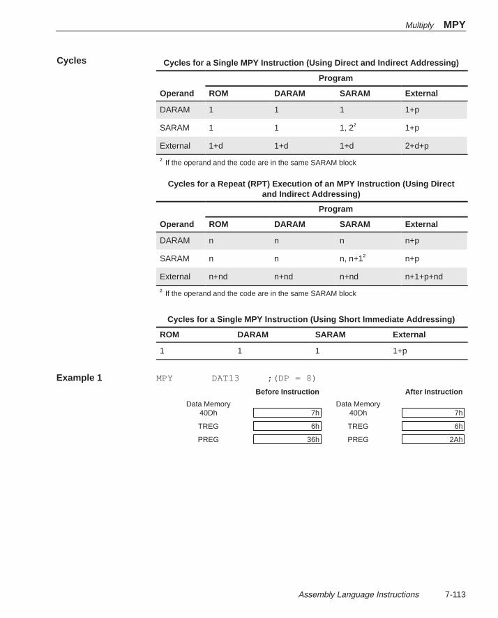
Multiply MPY
7-113 Assembly Language Instructions
Cycles for a Single MPY Instruction (Using Direct and Indirect Addressing)
Program
Operand ROM DARAM SARAM External
DARAM 1 1 1 1+p
SARAM 1 1 1, 2† 1+p
External 1+d 1+d 1+d 2+d+p
† If the operand and the code are in the same SARAM block
Cycles for a Repeat (RPT) Execution of an MPY Instruction (Using Directand Indirect Addressing)
Program
Operand ROM DARAM SARAM External
DARAM n n n n+p
SARAM n n n, n+1† n+p
External n+nd n+nd n+nd n+1+p+nd
† If the operand and the code are in the same SARAM block
Cycles for a Single MPY Instruction (Using Short Immediate Addressing)
ROM DARAM SARAM External
1 1 1 1+p
Example 1 MPY DAT13 ;(DP = 8)
Before Instruction After Instruction
Data Memory Data Memory40Dh 7h 40Dh 7h
TREG 6h TREG 6h
PREG 36h PREG 2Ah
Cycles
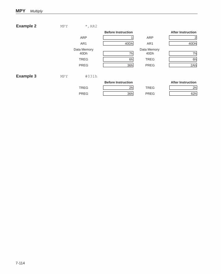
MPY Multiply
7-114
Example 2 MPY *,AR2
Before Instruction After Instruction
ARP 1 ARP 2
AR1 40Dh AR1 40Dh
Data Memory Data Memory 40Dh 7h 40Dh 7h
TREG 6h TREG 6h
PREG 36h PREG 2Ah
Example 3 MPY #031h
Before Instruction After Instruction
TREG 2h TREG 2h
PREG 36h PREG 62h
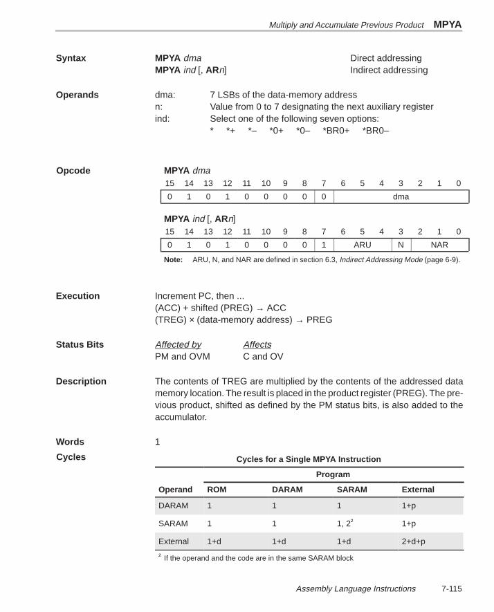
Multiply and Accumulate Previous Product MPYA
7-115 Assembly Language Instructions
Syntax MPYA dma Direct addressingMPYA ind [, ARn] Indirect addressing
Operands dma: 7 LSBs of the data-memory addressn: Value from 0 to 7 designating the next auxiliary registerind: Select one of the following seven options:
* *+ *– *0+ *0– *BR0+ *BR0–
MPYA dma15 14 13 12 11 10 9 8 7 6 5 4 3 2 1 0
0 1 0 1 0 0 0 0 0 dma
MPYA ind [, ARn]15 14 13 12 11 10 9 8 7 6 5 4 3 2 1 0
0 1 0 1 0 0 0 0 1 ARU N NAR
Note: ARU, N, and NAR are defined in section 6.3, Indirect Addressing Mode (page 6-9).
Execution Increment PC, then ...(ACC) + shifted (PREG) → ACC(TREG) × (data-memory address) → PREG
Status Bits Affected by AffectsPM and OVM C and OV
Description The contents of TREG are multiplied by the contents of the addressed datamemory location. The result is placed in the product register (PREG). The pre-vious product, shifted as defined by the PM status bits, is also added to theaccumulator.
Words 1
Cycles for a Single MPYA Instruction
Program
Operand ROM DARAM SARAM External
DARAM 1 1 1 1+p
SARAM 1 1 1, 2† 1+p
External 1+d 1+d 1+d 2+d+p
† If the operand and the code are in the same SARAM block
Opcode
Cycles
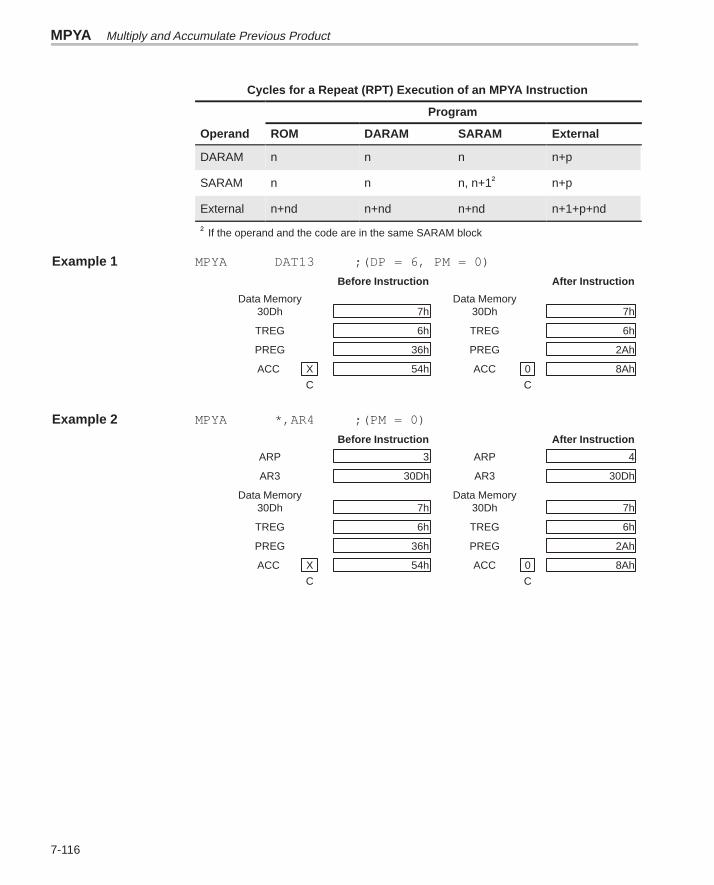
MPYA Multiply and Accumulate Previous Product
7-116
Cycles for a Repeat (RPT) Execution of an MPYA Instruction
Program
Operand ROM DARAM SARAM External
DARAM n n n n+p
SARAM n n n, n+1† n+p
External n+nd n+nd n+nd n+1+p+nd
† If the operand and the code are in the same SARAM block
Example 1 MPYA DAT13 ;(DP = 6, PM = 0)
Before Instruction After Instruction
Data Memory Data Memory30Dh 7h 30Dh 7h
TREG 6h TREG 6h
PREG 36h PREG 2Ah
ACC X 54h ACC 0 8Ah
C C
Example 2 MPYA *,AR4 ;(PM = 0)
Before Instruction After Instruction
ARP 3 ARP 4
AR3 30Dh AR3 30Dh
Data Memory Data Memory30Dh 7h 30Dh 7h
TREG 6h TREG 6h
PREG 36h PREG 2Ah
ACC X 54h ACC 0 8Ah
C C
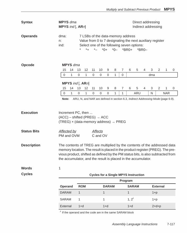
Multiply and Subtract Previous Product MPYS
7-117 Assembly Language Instructions
Syntax MPYS dma Direct addressingMPYS ind [, ARn] Indirect addressing
Operands dma: 7 LSBs of the data-memory addressn: Value from 0 to 7 designating the next auxiliary registerind: Select one of the following seven options:
* *+ *– *0+ *0– *BR0+ *BR0–
MPYS dma15 14 13 12 11 10 9 8 7 6 5 4 3 2 1 0
0 1 0 1 0 0 0 1 0 dma
MPYS ind [, ARn]15 14 13 12 11 10 9 8 7 6 5 4 3 2 1 0
0 1 0 1 0 0 0 1 1 ARU N NAR
Note: ARU, N, and NAR are defined in section 6.3, Indirect Addressing Mode (page 6-9).
Execution Increment PC, then ...(ACC) – shifted (PREG) → ACC(TREG) × (data-memory address) → PREG
Status Bits Affected by AffectsPM and OVM C and OV
Description The contents of TREG are multiplied by the contents of the addressed datamemory location. The result is placed in the product register (PREG). The pre-vious product, shifted as defined by the PM status bits, is also subtracted fromthe accumulator, and the result is placed in the accumulator.
Words 1
Cycles for a Single MPYS Instruction
Program
Operand ROM DARAM SARAM External
DARAM 1 1 1 1+p
SARAM 1 1 1, 2† 1+p
External 1+d 1+d 1+d 2+d+p
† If the operand and the code are in the same SARAM block
Opcode
Cycles

MPYS Multiply and Subtract Previous Product
7-118
Cycles for a Repeat (RPT) Execution of an MPYS Instruction
Program
Operand ROM DARAM SARAM External
DARAM n n n n+p
SARAM n n n, n+1† n+p
External n+nd n+nd n+nd n+1+p+nd
† If the operand and the code are in the same SARAM block
Example 1 MPYS DAT13 ;(DP = 6, PM = 0)
Before Instruction After Instruction
Data Memory Data Memory30Dh 7h 30Dh 7h
TREG 6h TREG 6h
PREG 36h PREG 2Ah
ACC X 54h ACC 1 1Eh
C C
Example 2 MPYS *,AR5 ;(PM = 0)
Before Instruction After Instruction
ARP 4 ARP 5
AR4 30Dh AR4 30Dh
Data Memory Data Memory30Dh 7h 30Dh 7h
TREG 6h TREG 6h
PREG 36h PREG 2Ah
ACC X 54h ACC 1 1Eh
C C
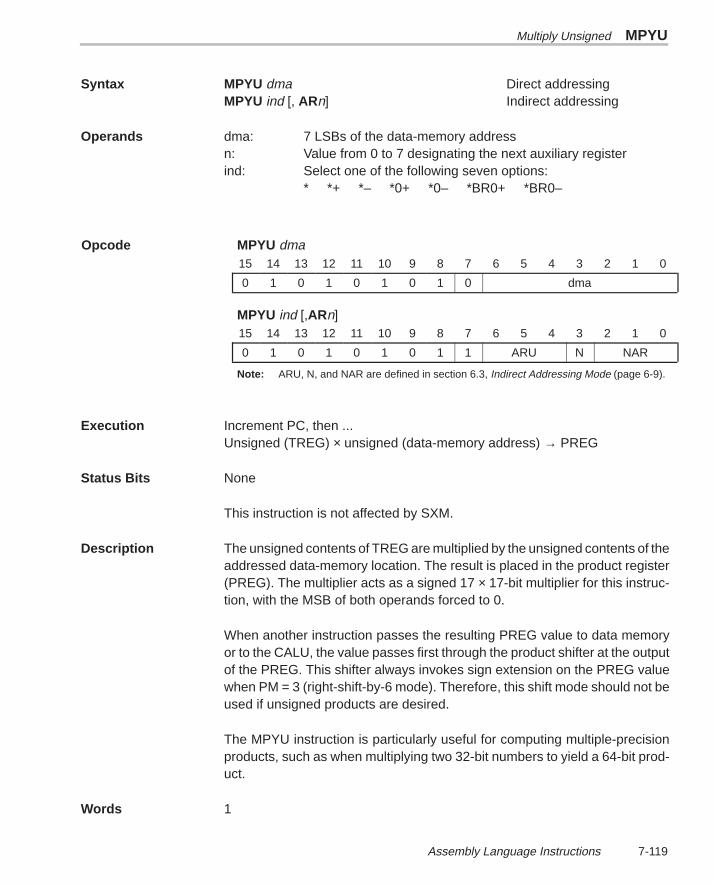
Multiply Unsigned MPYU
7-119 Assembly Language Instructions
Syntax MPYU dma Direct addressingMPYU ind [, ARn] Indirect addressing
Operands dma: 7 LSBs of the data-memory addressn: Value from 0 to 7 designating the next auxiliary registerind: Select one of the following seven options:
* *+ *– *0+ *0– *BR0+ *BR0–
MPYU dma15 14 13 12 11 10 9 8 7 6 5 4 3 2 1 0
0 1 0 1 0 1 0 1 0 dma
MPYU ind [,ARn]15 14 13 12 11 10 9 8 7 6 5 4 3 2 1 0
0 1 0 1 0 1 0 1 1 ARU N NAR
Note: ARU, N, and NAR are defined in section 6.3, Indirect Addressing Mode (page 6-9).
Execution Increment PC, then ...Unsigned (TREG) × unsigned (data-memory address) → PREG
Status Bits None
This instruction is not affected by SXM.
Description The unsigned contents of TREG are multiplied by the unsigned contents of theaddressed data-memory location. The result is placed in the product register(PREG). The multiplier acts as a signed 17 × 17-bit multiplier for this instruc-tion, with the MSB of both operands forced to 0.
When another instruction passes the resulting PREG value to data memoryor to the CALU, the value passes first through the product shifter at the outputof the PREG. This shifter always invokes sign extension on the PREG valuewhen PM = 3 (right-shift-by-6 mode). Therefore, this shift mode should not beused if unsigned products are desired.
The MPYU instruction is particularly useful for computing multiple-precisionproducts, such as when multiplying two 32-bit numbers to yield a 64-bit prod-uct.
Words 1
Opcode
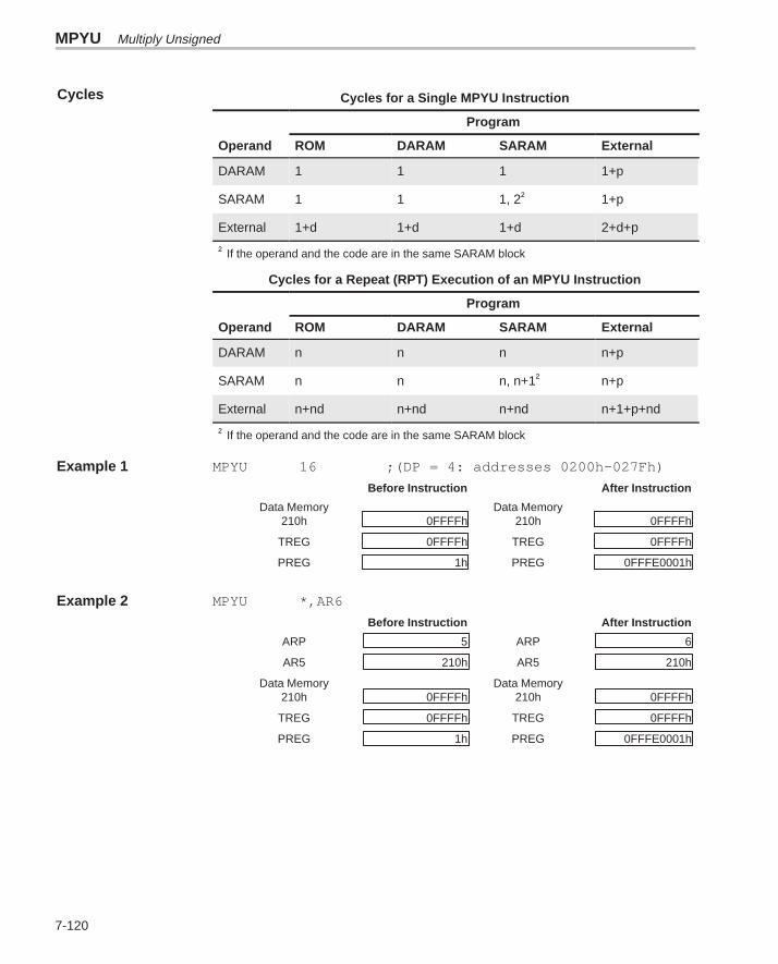
MPYU Multiply Unsigned
7-120
Cycles for a Single MPYU Instruction
Program
Operand ROM DARAM SARAM External
DARAM 1 1 1 1+p
SARAM 1 1 1, 2† 1+p
External 1+d 1+d 1+d 2+d+p
† If the operand and the code are in the same SARAM block
Cycles for a Repeat (RPT) Execution of an MPYU Instruction
Program
Operand ROM DARAM SARAM External
DARAM n n n n+p
SARAM n n n, n+1† n+p
External n+nd n+nd n+nd n+1+p+nd
† If the operand and the code are in the same SARAM block
Example 1 MPYU 16 ;(DP = 4: addresses 0200h–027Fh)
Before Instruction After Instruction
Data Memory Data Memory210h 0FFFFh 210h 0FFFFh
TREG 0FFFFh TREG 0FFFFh
PREG 1h PREG 0FFFE0001h
Example 2 MPYU *,AR6
Before Instruction After Instruction
ARP 5 ARP 6
AR5 210h AR5 210h
Data Memory Data Memory210h 0FFFFh 210h 0FFFFh
TREG 0FFFFh TREG 0FFFFh
PREG 1h PREG 0FFFE0001h
Cycles
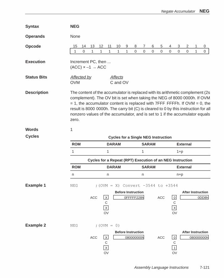
Negate Accumulator NEG
7-121 Assembly Language Instructions
Syntax NEG
Operands None
Opcode 01234567891011121314150100000001111101
Execution Increment PC, then ...(ACC) × –1 → ACC
Status Bits Affected by AffectsOVM C and OV
Description The content of the accumulator is replaced with its arithmetic complement (2scomplement). The OV bit is set when taking the NEG of 8000 0000h. If OVM= 1, the accumulator content is replaced with 7FFF FFFFh. If OVM = 0, theresult is 8000 0000h. The carry bit (C) is cleared to 0 by this instruction for allnonzero values of the accumulator, and is set to 1 if the accumulator equalszero.
Words 1
Cycles for a Single NEG Instruction
ROM DARAM SARAM External
1 1 1 1+p
Cycles for a Repeat (RPT) Execution of an NEG Instruction
ROM DARAM SARAM External
n n n n+p
Example 1 NEG ;(OVM = X) Convert –3544 to +3544
Before Instruction After Instruction
ACC X 0FFFFF228h ACC 0 0DD8h
C C
X X
OV OV
Example 2 NEG ;(OVM = 0)
Before Instruction After Instruction
ACC X 080000000h ACC 0 080000000h
C C
X 1
OV OV
Cycles
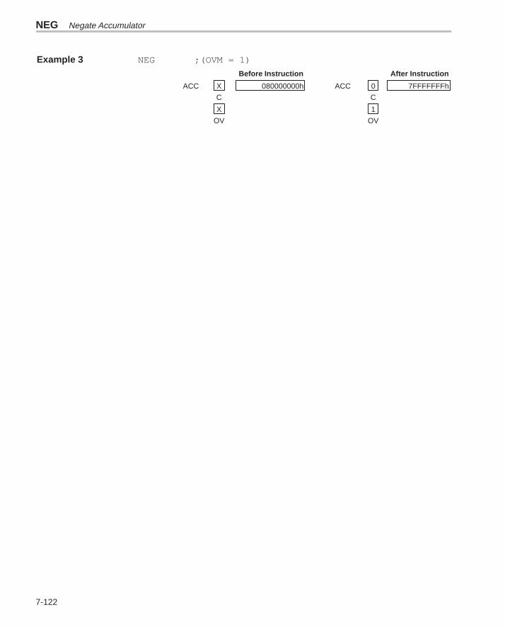
NEG Negate Accumulator
7-122
Example 3 NEG ;(OVM = 1)
Before Instruction After Instruction
ACC X 080000000h ACC 0 7FFFFFFFh
C C
X 1
OV OV
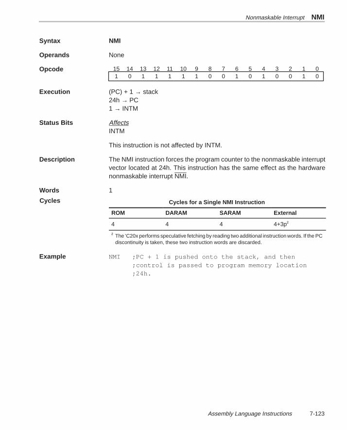
Nonmaskable Interrupt NMI
7-123 Assembly Language Instructions
Syntax NMI
Operands None
Opcode 01234567891011121314150100101001111101
Execution (PC) + 1 → stack24h → PC1 → INTM
Status Bits AffectsINTM
This instruction is not affected by INTM.
Description The NMI instruction forces the program counter to the nonmaskable interruptvector located at 24h. This instruction has the same effect as the hardwarenonmaskable interrupt NMI.
Words 1
Cycles for a Single NMI Instruction
ROM DARAM SARAM External
4 4 4 4+3p†
† The ’C20x performs speculative fetching by reading two additional instruction words. If the PCdiscontinuity is taken, these two instruction words are discarded.
Example NMI ;PC + 1 is pushed onto the stack, and then;control is passed to program memory location;24h.
Cycles
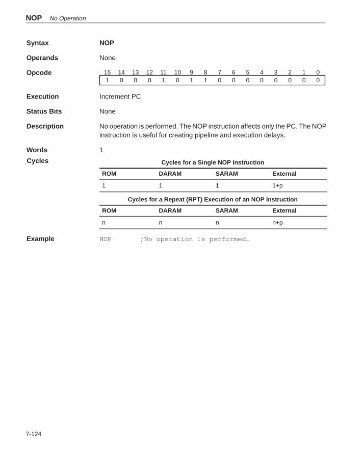
NOP No Operation
7-124
Syntax NOP
Operands None
Opcode 01234567891011121314150000000011010001
Execution Increment PC
Status Bits None
Description No operation is performed. The NOP instruction affects only the PC. The NOPinstruction is useful for creating pipeline and execution delays.
Words 1
Cycles for a Single NOP Instruction
ROM DARAM SARAM External
1 1 1 1+p
Cycles for a Repeat (RPT) Execution of an NOP Instruction
ROM DARAM SARAM External
n n n n+p
Example NOP ;No operation is performed.
Cycles
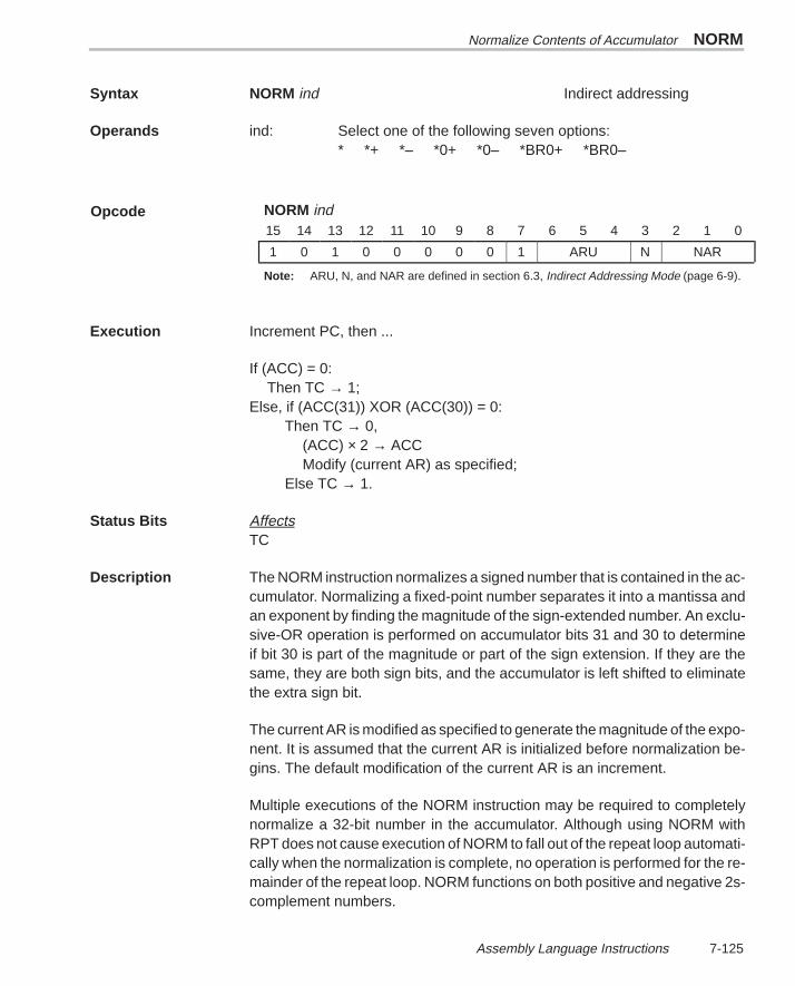
Normalize Contents of Accumulator NORM
7-125 Assembly Language Instructions
Syntax NORM ind Indirect addressing
Operands ind: Select one of the following seven options:* *+ *– *0+ *0– *BR0+ *BR0–
NORM ind15 14 13 12 11 10 9 8 7 6 5 4 3 2 1 0
1 0 1 0 0 0 0 0 1 ARU N NAR
Note: ARU, N, and NAR are defined in section 6.3, Indirect Addressing Mode (page 6-9).
Execution Increment PC, then ...
If (ACC) = 0:Then TC → 1;
Else, if (ACC(31)) XOR (ACC(30)) = 0:Then TC → 0,
(ACC) × 2 → ACCModify (current AR) as specified;
Else TC → 1.
Status Bits AffectsTC
Description The NORM instruction normalizes a signed number that is contained in the ac-cumulator. Normalizing a fixed-point number separates it into a mantissa andan exponent by finding the magnitude of the sign-extended number. An exclu-sive-OR operation is performed on accumulator bits 31 and 30 to determineif bit 30 is part of the magnitude or part of the sign extension. If they are thesame, they are both sign bits, and the accumulator is left shifted to eliminatethe extra sign bit.
The current AR is modified as specified to generate the magnitude of the expo-nent. It is assumed that the current AR is initialized before normalization be-gins. The default modification of the current AR is an increment.
Multiple executions of the NORM instruction may be required to completelynormalize a 32-bit number in the accumulator. Although using NORM withRPT does not cause execution of NORM to fall out of the repeat loop automati-cally when the normalization is complete, no operation is performed for the re-mainder of the repeat loop. NORM functions on both positive and negative 2s-complement numbers.
Opcode
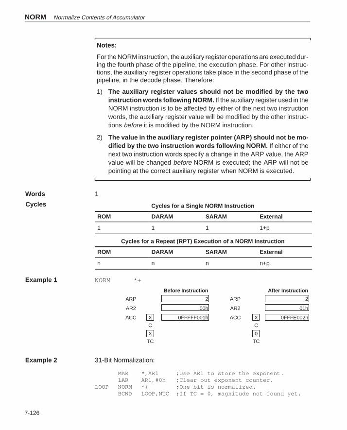
NORM Normalize Contents of Accumulator
7-126
Notes:
For the NORM instruction, the auxiliary register operations are executed dur-ing the fourth phase of the pipeline, the execution phase. For other instruc-tions, the auxiliary register operations take place in the second phase of thepipeline, in the decode phase. Therefore:
1) The auxiliary register values should not be modified by the twoinstruction words following NORM. If the auxiliary register used in theNORM instruction is to be affected by either of the next two instructionwords, the auxiliary register value will be modified by the other instruc-tions before it is modified by the NORM instruction.
2) The value in the auxiliary register pointer (ARP) should not be mo-dified by the two instruction words following NORM. If either of thenext two instruction words specify a change in the ARP value, the ARPvalue will be changed before NORM is executed; the ARP will not bepointing at the correct auxiliary register when NORM is executed.
Words 1
Cycles for a Single NORM Instruction
ROM DARAM SARAM External
1 1 1 1+p
Cycles for a Repeat (RPT) Execution of a NORM Instruction
ROM DARAM SARAM External
n n n n+p
Example 1 NORM *+
Before Instruction After Instruction
ARP 2 ARP 2
AR2 00h AR2 01h
ACC X 0FFFFF001h ACC X 0FFFE002h
C C
X 0
TC TC
Example 2 31-Bit Normalization:
MAR *,AR1 ;Use AR1 to store the exponent.LAR AR1,#0h ;Clear out exponent counter.
LOOP NORM *+ ;One bit is normalized.BCND LOOP,NTC ;If TC = 0, magnitude not found yet.
Cycles
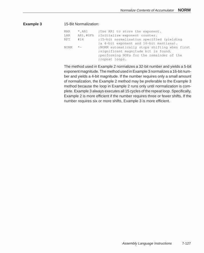
Normalize Contents of Accumulator NORM
7-127 Assembly Language Instructions
Example 3 15-Bit Normalization:
MAR *,AR1 ;Use AR1 to store the exponent.LAR AR1,#0Fh ;Initialize exponent counter.RPT #14 ;15-bit normalization specified (yielding
;a 4-bit exponent and 16-bit mantissa).NORM *– ;NORM automatically stops shifting when first
;significant magnitude bit is found,;performing NOPs for the remainder of the;repeat loops.
The method used in Example 2 normalizes a 32-bit number and yields a 5-bitexponent magnitude. The method used in Example 3 normalizes a 16-bit num-ber and yields a 4-bit magnitude. If the number requires only a small amountof normalization, the Example 2 method may be preferable to the Example 3method because the loop in Example 2 runs only until normalization is com-plete. Example 3 always executes all 15 cycles of the repeat loop. Specifically,Example 2 is more efficient if the number requires three or fewer shifts. If thenumber requires six or more shifts, Example 3 is more efficient.
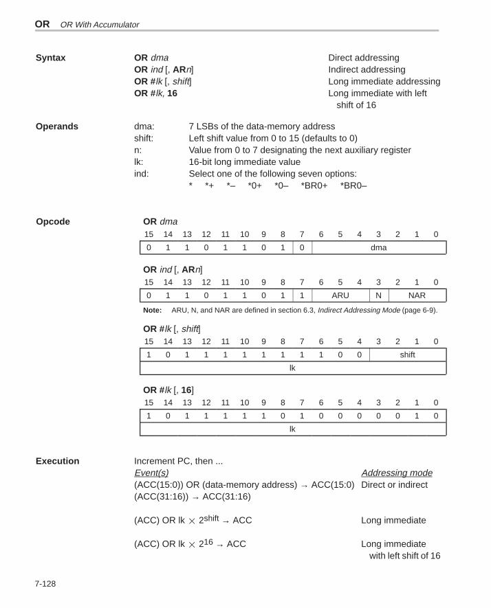
OR OR With Accumulator
7-128
Syntax OR dma Direct addressingOR ind [, ARn] Indirect addressingOR #lk [, shift] Long immediate addressingOR #lk, 16 Long immediate with left
shift of 16
Operands dma: 7 LSBs of the data-memory addressshift: Left shift value from 0 to 15 (defaults to 0)n: Value from 0 to 7 designating the next auxiliary registerlk: 16-bit long immediate valueind: Select one of the following seven options:
* *+ *– *0+ *0– *BR0+ *BR0–
OR dma15 14 13 12 11 10 9 8 7 6 5 4 3 2 1 0
0 1 1 0 1 1 0 1 0 dma
OR ind [, ARn]15 14 13 12 11 10 9 8 7 6 5 4 3 2 1 0
0 1 1 0 1 1 0 1 1 ARU N NAR
Note: ARU, N, and NAR are defined in section 6.3, Indirect Addressing Mode (page 6-9).
OR #lk [, shift]15 14 13 12 11 10 9 8 7 6 5 4 3 2 1 0
1 0 1 1 1 1 1 1 1 1 0 0 shift
lk
OR #lk [, 16]15 14 13 12 11 10 9 8 7 6 5 4 3 2 1 0
1 0 1 1 1 1 1 0 1 0 0 0 0 0 1 0
lk
Execution Increment PC, then ...Event(s) Addressing mode(ACC(15:0)) OR (data-memory address) → ACC(15:0) Direct or indirect(ACC(31:16)) → ACC(31:16)
(ACC) OR lk 2shift → ACC Long immediate
(ACC) OR lk 216 → ACC Long immediatewith left shift of 16
Opcode
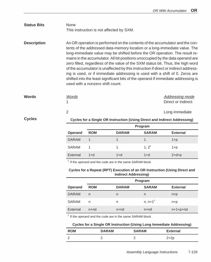
OR With Accumulator OR
7-129 Assembly Language Instructions
Status Bits NoneThis instruction is not affected by SXM.
Description An OR operation is performed on the contents of the accumulator and the con-tents of the addressed data-memory location or a long-immediate value. Thelong-immediate value may be shifted before the OR operation. The result re-mains in the accumulator. All bit positions unoccupied by the data operand arezero filled, regardless of the value of the SXM status bit. Thus, the high wordof the accumulator is unaffected by this instruction if direct or indirect address-ing is used, or if immediate addressing is used with a shift of 0. Zeros areshifted into the least significant bits of the operand if immediate addressing isused with a nonzero shift count.
Words Words Addressing mode1 Direct or indirect
2 Long immediate
Cycles for a Single OR Instruction (Using Direct and Indirect Addressing)
Program
Operand ROM DARAM SARAM External
DARAM 1 1 1 1+p
SARAM 1 1 1, 2† 1+p
External 1+d 1+d 1+d 2+d+p
† If the operand and the code are in the same SARAM block
Cycles for a Repeat (RPT) Execution of an OR Instruction (Using Direct andIndirect Addressing)
Program
Operand ROM DARAM SARAM External
DARAM n n n n+p
SARAM n n n, n+1† n+p
External n+nd n+nd n+nd n+1+p+nd
† If the operand and the code are in the same SARAM block
Cycles for a Single OR Instruction (Using Long Immediate Addressing)
ROM DARAM SARAM External
2 2 2 2+2p
Cycles
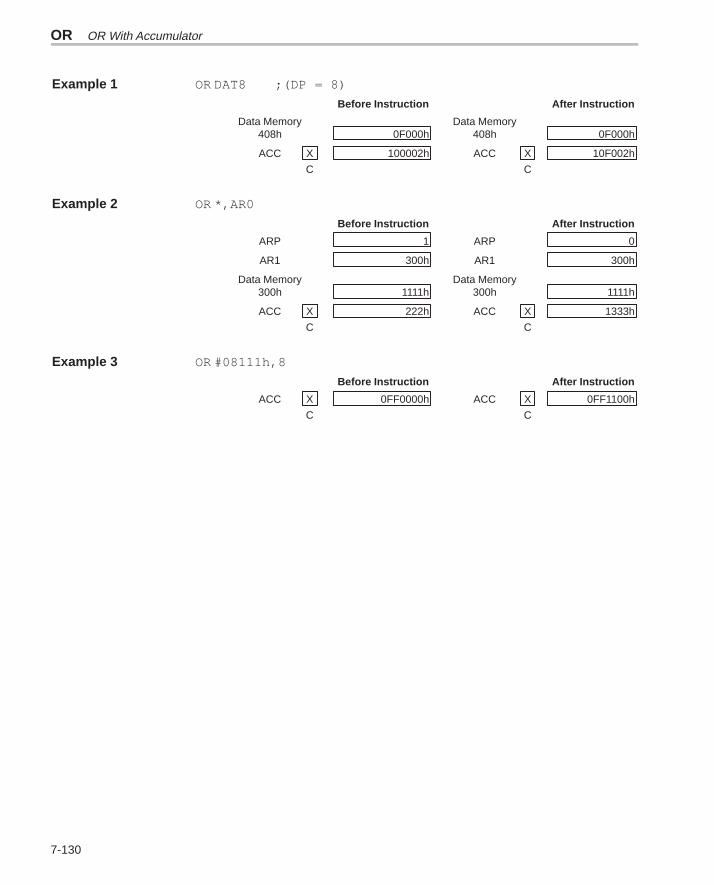
OR OR With Accumulator
7-130
Example 1 OR DAT8 ;(DP = 8)
Before Instruction After Instruction
Data Memory Data Memory408h 0F000h 408h 0F000h
ACC X 100002h ACC X 10F002h
C C
Example 2 OR *,AR0
Before Instruction After Instruction
ARP 1 ARP 0
AR1 300h AR1 300h
Data Memory Data Memory300h 1111h 300h 1111h
ACC X 222h ACC X 1333h
C C
Example 3 OR #08111h,8
Before Instruction After Instruction
ACC X 0FF0000h ACC X 0FF1100h
C C
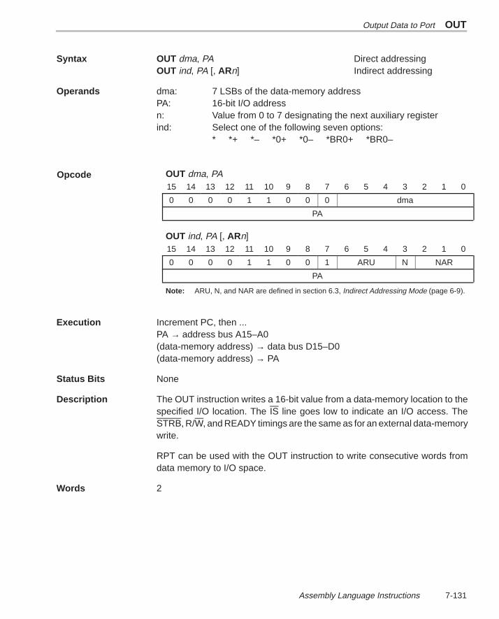
Output Data to Port OUT
7-131 Assembly Language Instructions
Syntax OUT dma, PA Direct addressingOUT ind, PA [, ARn] Indirect addressing
Operands dma: 7 LSBs of the data-memory addressPA: 16-bit I/O addressn: Value from 0 to 7 designating the next auxiliary registerind: Select one of the following seven options:
* *+ *– *0+ *0– *BR0+ *BR0–
OUT dma, PA15 14 13 12 11 10 9 8 7 6 5 4 3 2 1 0
0 0 0 0 1 1 0 0 0 dma
PA
OUT ind, PA [, ARn]15 14 13 12 11 10 9 8 7 6 5 4 3 2 1 0
0 0 0 0 1 1 0 0 1 ARU N NAR
PA
Note: ARU, N, and NAR are defined in section 6.3, Indirect Addressing Mode (page 6-9).
Execution Increment PC, then ...PA → address bus A15–A0(data-memory address) → data bus D15–D0(data-memory address) → PA
Status Bits None
Description The OUT instruction writes a 16-bit value from a data-memory location to thespecified I/O location. The IS line goes low to indicate an I/O access. TheSTRB, R/W, and READY timings are the same as for an external data-memorywrite.
RPT can be used with the OUT instruction to write consecutive words fromdata memory to I/O space.
Words 2
Opcode
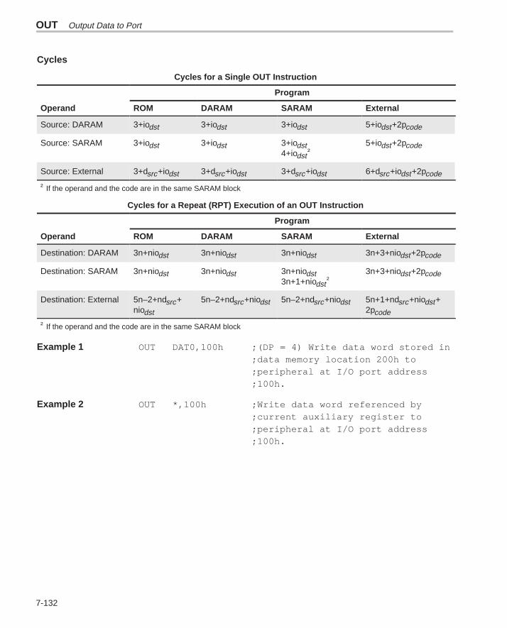
OUT Output Data to Port
7-132
Cycles
Cycles for a Single OUT Instruction
Program
Operand ROM DARAM SARAM External
Source: DARAM 3+iodst 3+iodst 3+iodst 5+iodst+2pcode
Source: SARAM 3+iodst 3+iodst 3+iodst4+iodst†
5+iodst+2pcode
Source: External 3+dsrc+iodst 3+dsrc+iodst 3+dsrc+iodst 6+dsrc+iodst+2pcode
† If the operand and the code are in the same SARAM block
Cycles for a Repeat (RPT) Execution of an OUT Instruction
Program
Operand ROM DARAM SARAM External
Destination: DARAM 3n+niodst 3n+niodst 3n+niodst 3n+3+niodst+2pcode
Destination: SARAM 3n+niodst 3n+niodst 3n+niodst3n+1+niodst†
3n+3+niodst+2pcode
Destination: External 5n–2+ndsrc+niodst
5n–2+ndsrc+niodst 5n–2+ndsrc+niodst 5n+1+ndsrc+niodst+2pcode
† If the operand and the code are in the same SARAM block
Example 1 OUT DAT0,100h ;(DP = 4) Write data word stored in;data memory location 200h to;peripheral at I/O port address;100h.
Example 2 OUT *,100h ;Write data word referenced by;current auxiliary register to;peripheral at I/O port address;100h.
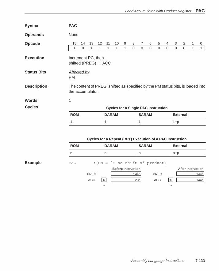
Load Accumulator With Product Register PAC
7-133 Assembly Language Instructions
Syntax PAC
Operands None
Opcode 01234567891011121314151100000001111101
Execution Increment PC, then ...shifted (PREG) → ACC
Status Bits Affected byPM
Description The content of PREG, shifted as specified by the PM status bits, is loaded intothe accumulator.
Words 1
Cycles for a Single PAC Instruction
ROM DARAM SARAM External
1 1 1 1+p
Cycles for a Repeat (RPT) Execution of a PAC Instruction
ROM DARAM SARAM External
n n n n+p
Example PAC ;(PM = 0: no shift of product)
Before Instruction After Instruction
PREG 144h PREG 144h
ACC X 23h ACC X 144h
C C
Cycles
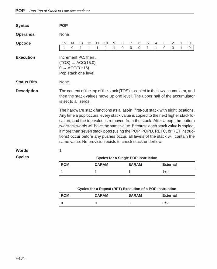
POP Pop Top of Stack to Low Accumulator
7-134
Syntax POP
Operands None
Opcode 01234567891011121314150100110001111101
Execution Increment PC, then ...(TOS) → ACC(15:0)0 → ACC(31:16)Pop stack one level
Status Bits None
Description The content of the top of the stack (TOS) is copied to the low accumulator, andthen the stack values move up one level. The upper half of the accumulatoris set to all zeros.
The hardware stack functions as a last-in, first-out stack with eight locations.Any time a pop occurs, every stack value is copied to the next higher stack lo-cation, and the top value is removed from the stack. After a pop, the bottomtwo stack words will have the same value. Because each stack value is copied,if more than seven stack pops (using the POP, POPD, RETC, or RET instruc-tions) occur before any pushes occur, all levels of the stack will contain thesame value. No provision exists to check stack underflow.
Words 1
Cycles for a Single POP Instruction
ROM DARAM SARAM External
1 1 1 1+p
Cycles for a Repeat (RPT) Execution of a POP Instruction
ROM DARAM SARAM External
n n n n+p
Cycles
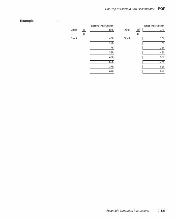
Pop Top of Stack to Low Accumulator POP
7-135 Assembly Language Instructions
Example POP
Before Instruction After Instruction
ACC X 82h ACC X 45h
C C
Stack 45h Stack 16h
16h 7h
7h 33h
33h 42h
42h 56h
56h 37h
37h 61h
61h 61h
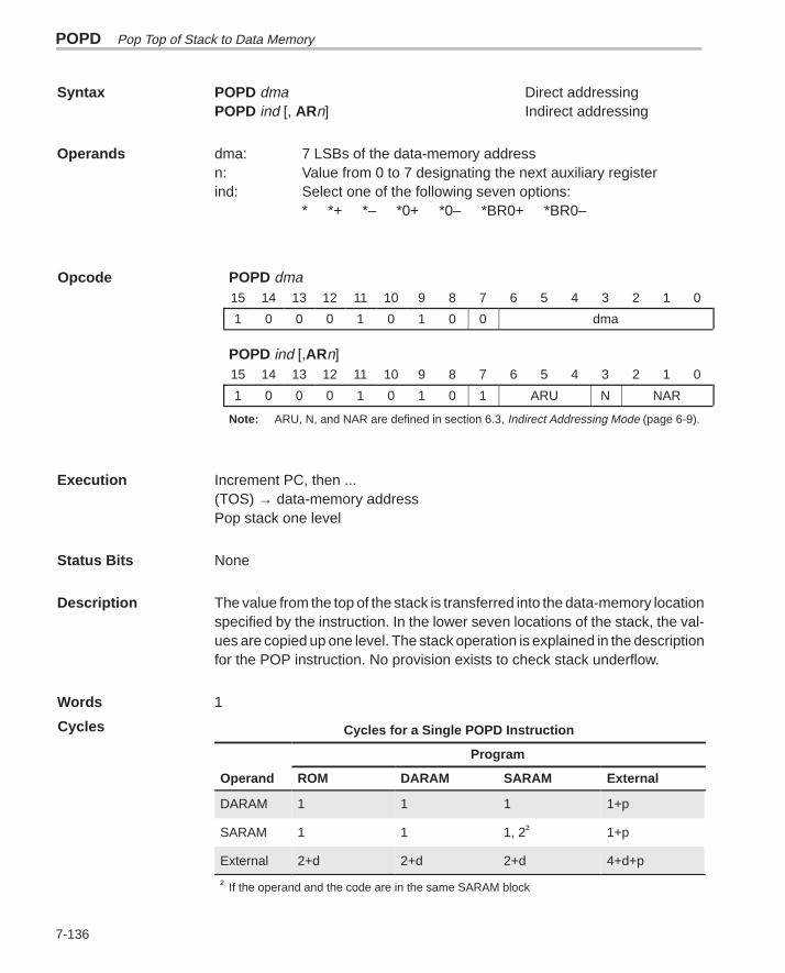
POPD Pop Top of Stack to Data Memory
7-136
Syntax POPD dma Direct addressingPOPD ind [, ARn] Indirect addressing
Operands dma: 7 LSBs of the data-memory addressn: Value from 0 to 7 designating the next auxiliary registerind: Select one of the following seven options:
* *+ *– *0+ *0– *BR0+ *BR0–
POPD dma15 14 13 12 11 10 9 8 7 6 5 4 3 2 1 0
1 0 0 0 1 0 1 0 0 dma
POPD ind [,ARn]15 14 13 12 11 10 9 8 7 6 5 4 3 2 1 0
1 0 0 0 1 0 1 0 1 ARU N NAR
Note: ARU, N, and NAR are defined in section 6.3, Indirect Addressing Mode (page 6-9).
Execution Increment PC, then ...(TOS) → data-memory addressPop stack one level
Status Bits None
Description The value from the top of the stack is transferred into the data-memory locationspecified by the instruction. In the lower seven locations of the stack, the val-ues are copied up one level. The stack operation is explained in the descriptionfor the POP instruction. No provision exists to check stack underflow.
Words 1
Cycles for a Single POPD Instruction
Program
Operand ROM DARAM SARAM External
DARAM 1 1 1 1+p
SARAM 1 1 1, 2† 1+p
External 2+d 2+d 2+d 4+d+p
† If the operand and the code are in the same SARAM block
Opcode
Cycles
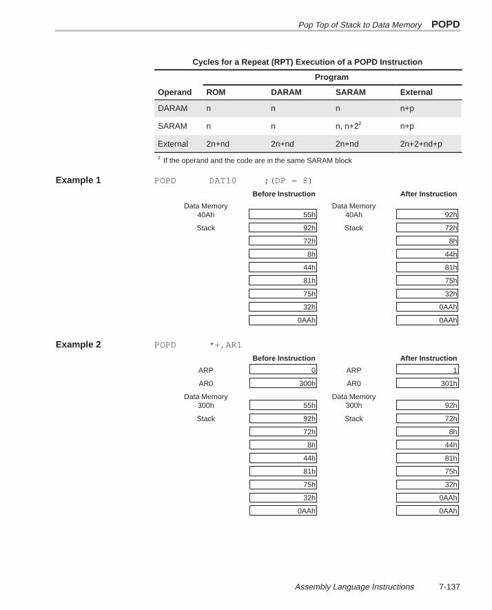
Pop Top of Stack to Data Memory POPD
7-137 Assembly Language Instructions
Cycles for a Repeat (RPT) Execution of a POPD Instruction
Program
Operand ROM DARAM SARAM External
DARAM n n n n+p
SARAM n n n, n+2† n+p
External 2n+nd 2n+nd 2n+nd 2n+2+nd+p
† If the operand and the code are in the same SARAM block
Example 1 POPD DAT10 ;(DP = 8)
Before Instruction After Instruction
Data Memory Data Memory40Ah 55h 40Ah 92h
Stack 92h Stack 72h
72h 8h
8h 44h
44h 81h
81h 75h
75h 32h
32h 0AAh
0AAh 0AAh
Example 2 POPD *+,AR1
Before Instruction After Instruction
ARP 0 ARP 1
AR0 300h AR0 301h
Data Memory Data Memory300h 55h 300h 92h
Stack 92h Stack 72h
72h 8h
8h 44h
44h 81h
81h 75h
75h 32h
32h 0AAh
0AAh 0AAh
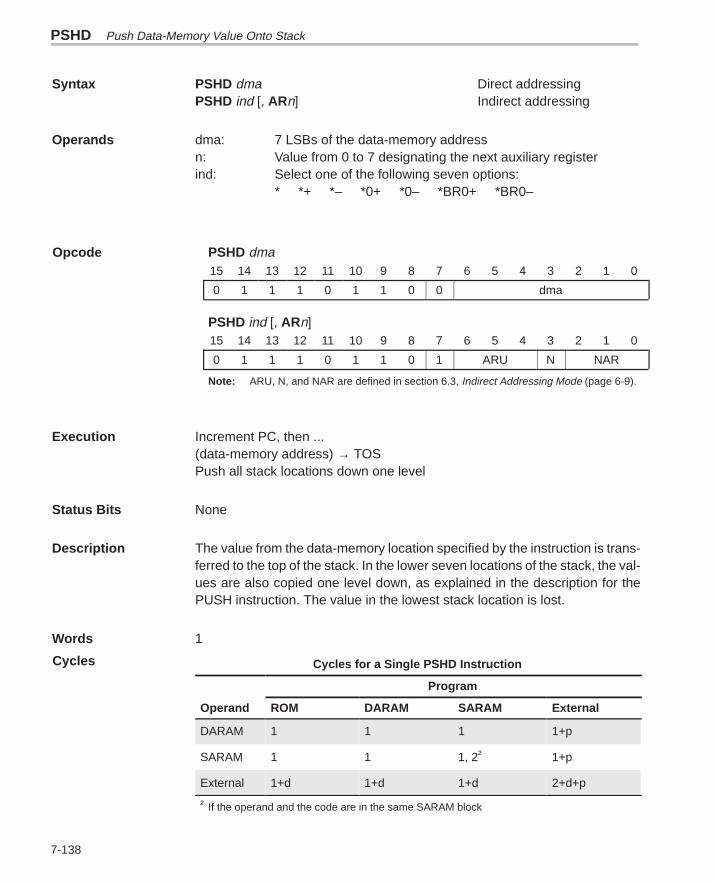
PSHD Push Data-Memory Value Onto Stack
7-138
Syntax PSHD dma Direct addressingPSHD ind [, ARn] Indirect addressing
Operands dma: 7 LSBs of the data-memory addressn: Value from 0 to 7 designating the next auxiliary registerind: Select one of the following seven options:
* *+ *– *0+ *0– *BR0+ *BR0–
PSHD dma15 14 13 12 11 10 9 8 7 6 5 4 3 2 1 0
0 1 1 1 0 1 1 0 0 dma
PSHD ind [, ARn]15 14 13 12 11 10 9 8 7 6 5 4 3 2 1 0
0 1 1 1 0 1 1 0 1 ARU N NAR
Note: ARU, N, and NAR are defined in section 6.3, Indirect Addressing Mode (page 6-9).
Execution Increment PC, then ...(data-memory address) → TOSPush all stack locations down one level
Status Bits None
Description The value from the data-memory location specified by the instruction is trans-ferred to the top of the stack. In the lower seven locations of the stack, the val-ues are also copied one level down, as explained in the description for thePUSH instruction. The value in the lowest stack location is lost.
Words 1
Cycles for a Single PSHD Instruction
Program
Operand ROM DARAM SARAM External
DARAM 1 1 1 1+p
SARAM 1 1 1, 2† 1+p
External 1+d 1+d 1+d 2+d+p
† If the operand and the code are in the same SARAM block
Opcode
Cycles
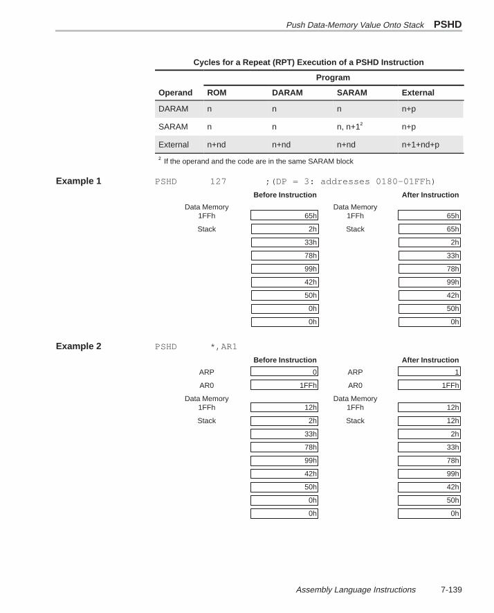
Push Data-Memory Value Onto Stack PSHD
7-139 Assembly Language Instructions
Cycles for a Repeat (RPT) Execution of a PSHD Instruction
Program
Operand ROM DARAM SARAM External
DARAM n n n n+p
SARAM n n n, n+1† n+p
External n+nd n+nd n+nd n+1+nd+p
† If the operand and the code are in the same SARAM block
Example 1 PSHD 127 ;(DP = 3: addresses 0180–01FFh)
Before Instruction After Instruction
Data Memory Data Memory1FFh 65h 1FFh 65h
Stack 2h Stack 65h
33h 2h
78h 33h
99h 78h
42h 99h
50h 42h
0h 50h
0h 0h
Example 2 PSHD *,AR1
Before Instruction After Instruction
ARP 0 ARP 1
AR0 1FFh AR0 1FFh
Data Memory Data Memory1FFh 12h 1FFh 12h
Stack 2h Stack 12h
33h 2h
78h 33h
99h 78h
42h 99h
50h 42h
0h 50h
0h 0h
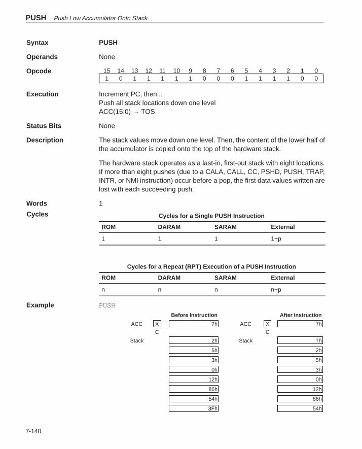
PUSH Push Low Accumulator Onto Stack
7-140
Syntax PUSH
Operands None
Opcode 01234567891011121314150011110001111101
Execution Increment PC, then...Push all stack locations down one levelACC(15:0) → TOS
Status Bits None
Description The stack values move down one level. Then, the content of the lower half ofthe accumulator is copied onto the top of the hardware stack.
The hardware stack operates as a last-in, first-out stack with eight locations.If more than eight pushes (due to a CALA, CALL, CC, PSHD, PUSH, TRAP,INTR, or NMI instruction) occur before a pop, the first data values written arelost with each succeeding push.
Words 1
Cycles for a Single PUSH Instruction
ROM DARAM SARAM External
1 1 1 1+p
Cycles for a Repeat (RPT) Execution of a PUSH Instruction
ROM DARAM SARAM External
n n n n+p
Example PUSH
Before Instruction After Instruction
ACC X 7h ACC X 7h
C C
Stack 2h Stack 7h
5h 2h
3h 5h
0h 3h
12h 0h
86h 12h
54h 86h
3Fh 54h
Cycles
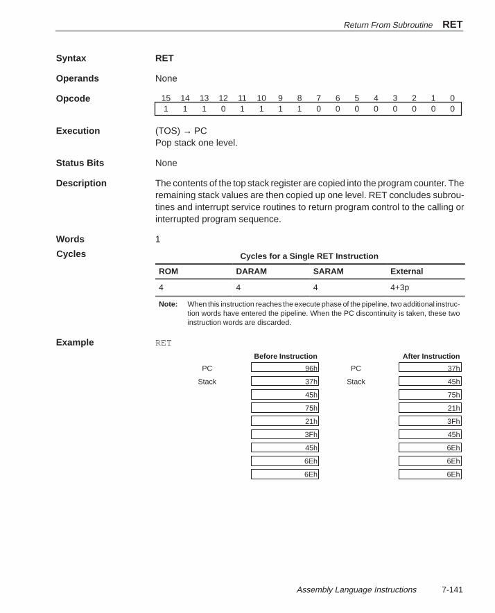
Return From Subroutine RET
7-141 Assembly Language Instructions
Syntax RET
Operands None
Opcode 01234567891011121314150000000011110111
Execution (TOS) → PCPop stack one level.
Status Bits None
Description The contents of the top stack register are copied into the program counter. Theremaining stack values are then copied up one level. RET concludes subrou-tines and interrupt service routines to return program control to the calling orinterrupted program sequence.
Words 1
Cycles for a Single RET Instruction
ROM DARAM SARAM External
4 4 4 4+3p
Note: When this instruction reaches the execute phase of the pipeline, two additional instruc-tion words have entered the pipeline. When the PC discontinuity is taken, these twoinstruction words are discarded.
Example RET
Before Instruction After Instruction
PC 96h PC 37h
Stack 37h Stack 45h
45h 75h
75h 21h
21h 3Fh
3Fh 45h
45h 6Eh
6Eh 6Eh
6Eh 6Eh
Cycles
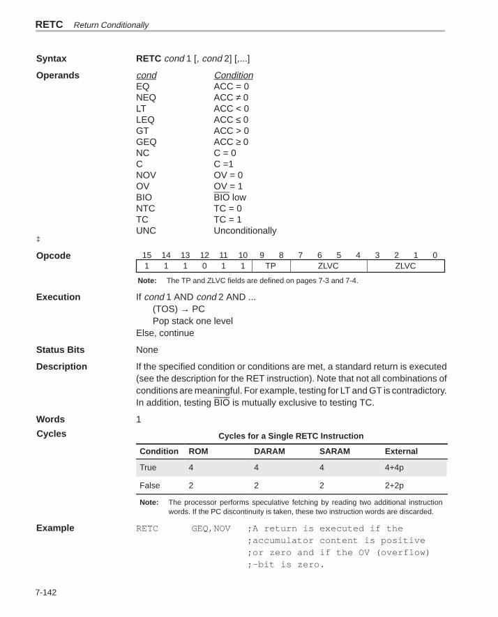
RETC Return Conditionally
7-142
Syntax RETC cond1 [, cond2] [,...]
Operands cond ConditionEQ ACC = 0NEQ ACC ≠ 0LT ACC < 0LEQ ACC ≤ 0GT ACC > 0GEQ ACC ≥ 0NC C = 0C C =1NOV OV = 0OV OV = 1BIO BIO lowNTC TC = 0TC TC = 1UNC Unconditionally
‡
Opcode 0123456789101112131415ZLVCZLVCTP110111
Note: The TP and ZLVC fields are defined on pages 7-3 and 7-4.
Execution If cond1 AND cond2 AND ...(TOS) → PCPop stack one level
Else, continue
Status Bits None
Description If the specified condition or conditions are met, a standard return is executed(see the description for the RET instruction). Note that not all combinations ofconditions are meaningful. For example, testing for LT and GT is contradictory.In addition, testing BIO is mutually exclusive to testing TC.
Words 1
Cycles for a Single RETC Instruction
Condition ROM DARAM SARAM External
True 4 4 4 4+4p
False 2 2 2 2+2p
Note: The processor performs speculative fetching by reading two additional instructionwords. If the PC discontinuity is taken, these two instruction words are discarded.
Example RETC GEQ,NOV ;A return is executed if the;accumulator content is positive;or zero and if the OV (overflow);-bit is zero.
Cycles
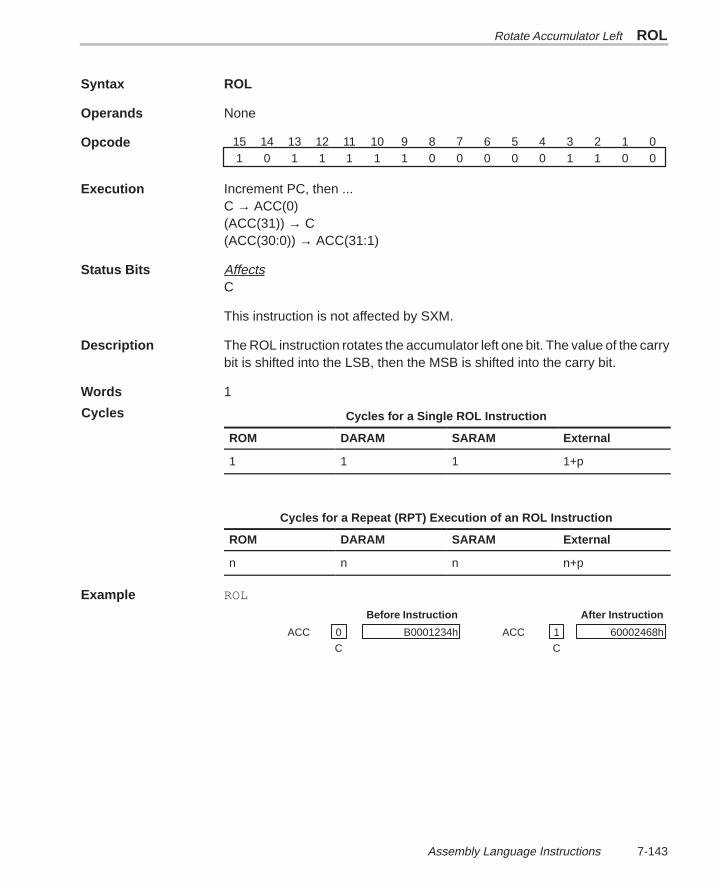
Rotate Accumulator Left ROL
7-143 Assembly Language Instructions
Syntax ROL
Operands None
Opcode 01234567891011121314150011000001111101
Execution Increment PC, then ...C → ACC(0)(ACC(31)) → C(ACC(30:0)) → ACC(31:1)
Status Bits Affects C
This instruction is not affected by SXM.
Description The ROL instruction rotates the accumulator left one bit. The value of the carrybit is shifted into the LSB, then the MSB is shifted into the carry bit.
Words 1
Cycles for a Single ROL Instruction
ROM DARAM SARAM External
1 1 1 1+p
Cycles for a Repeat (RPT) Execution of an ROL Instruction
ROM DARAM SARAM External
n n n n+p
Example ROL
Before Instruction After Instruction
ACC 0 B0001234h ACC 1 60002468h
C C
Cycles
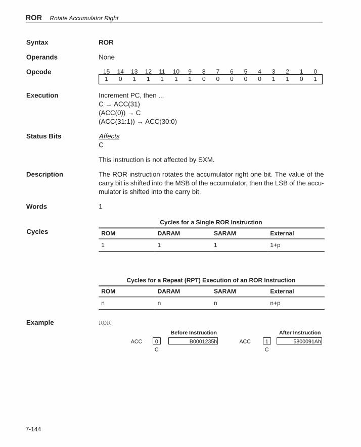
ROR Rotate Accumulator Right
7-144
Syntax ROR
Operands None
Opcode 01234567891011121314151011000001111101
Execution Increment PC, then ...C → ACC(31)(ACC(0)) → C(ACC(31:1)) → ACC(30:0)
Status Bits AffectsC
This instruction is not affected by SXM.
Description The ROR instruction rotates the accumulator right one bit. The value of thecarry bit is shifted into the MSB of the accumulator, then the LSB of the accu-mulator is shifted into the carry bit.
Words 1
Cycles for a Single ROR Instruction
ROM DARAM SARAM External
1 1 1 1+p
Cycles for a Repeat (RPT) Execution of an ROR Instruction
ROM DARAM SARAM External
n n n n+p
Example ROR
Before Instruction After Instruction
ACC 0 B0001235h ACC 1 5800091Ah
C C
Cycles
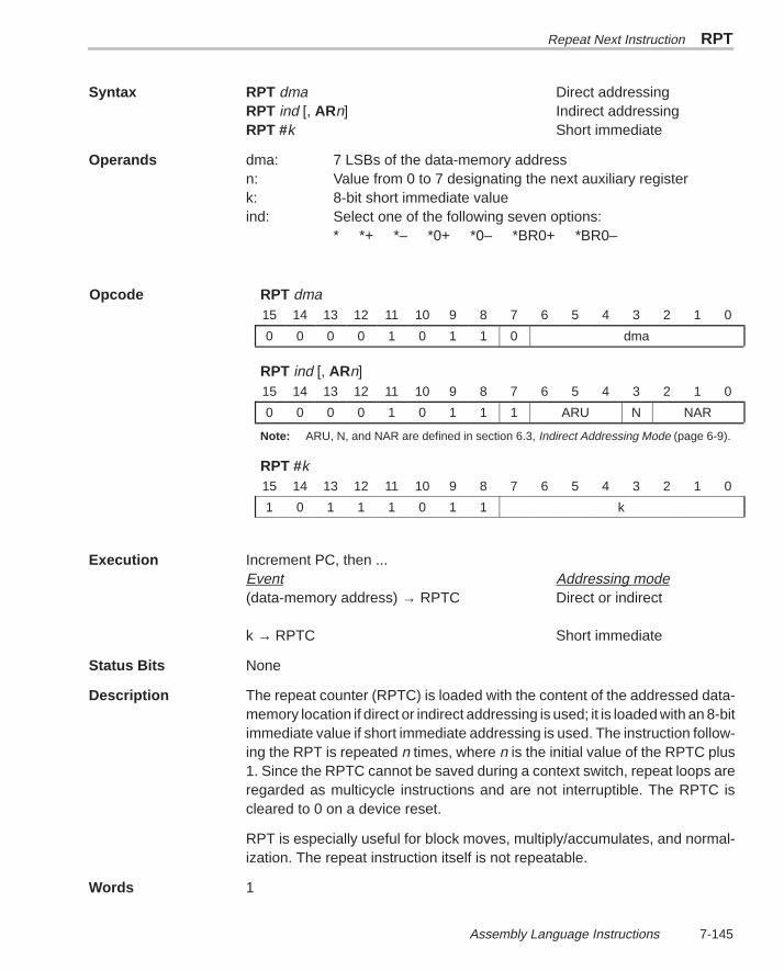
Repeat Next Instruction RPT
7-145 Assembly Language Instructions
Syntax RPT dma Direct addressingRPT ind [, ARn] Indirect addressingRPT #k Short immediate
Operands dma: 7 LSBs of the data-memory addressn: Value from 0 to 7 designating the next auxiliary registerk: 8-bit short immediate valueind: Select one of the following seven options:
* *+ *– *0+ *0– *BR0+ *BR0–
RPT dma15 14 13 12 11 10 9 8 7 6 5 4 3 2 1 0
0 0 0 0 1 0 1 1 0 dma
RPT ind [, ARn]15 14 13 12 11 10 9 8 7 6 5 4 3 2 1 0
0 0 0 0 1 0 1 1 1 ARU N NAR
Note: ARU, N, and NAR are defined in section 6.3, Indirect Addressing Mode (page 6-9).
RPT #k15 14 13 12 11 10 9 8 7 6 5 4 3 2 1 0
1 0 1 1 1 0 1 1 k
Execution Increment PC, then ...Event Addressing mode(data-memory address) → RPTC Direct or indirect
k → RPTC Short immediate
Status Bits None
Description The repeat counter (RPTC) is loaded with the content of the addressed data-memory location if direct or indirect addressing is used; it is loaded with an 8-bitimmediate value if short immediate addressing is used. The instruction follow-ing the RPT is repeated n times, where n is the initial value of the RPTC plus1. Since the RPTC cannot be saved during a context switch, repeat loops areregarded as multicycle instructions and are not interruptible. The RPTC iscleared to 0 on a device reset.
RPT is especially useful for block moves, multiply/accumulates, and normal-ization. The repeat instruction itself is not repeatable.
Words 1
Opcode
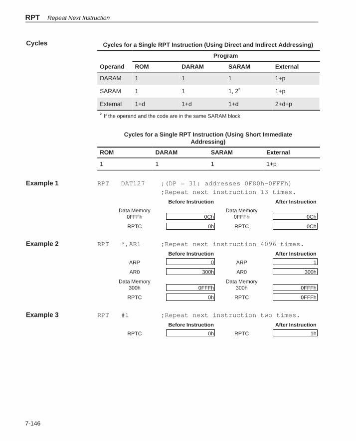
RPT Repeat Next Instruction
7-146
Cycles for a Single RPT Instruction (Using Direct and Indirect Addressing)
Program
Operand ROM DARAM SARAM External
DARAM 1 1 1 1+p
SARAM 1 1 1, 2† 1+p
External 1+d 1+d 1+d 2+d+p
† If the operand and the code are in the same SARAM block
Cycles for a Single RPT Instruction (Using Short ImmediateAddressing)
ROM DARAM SARAM External
1 1 1 1+p
Example 1 RPT DAT127 ;(DP = 31: addresses 0F80h–0FFFh);Repeat next instruction 13 times.
Before Instruction After Instruction
Data Memory Data Memory0FFFh 0Ch 0FFFh 0Ch
RPTC 0h RPTC 0Ch
Example 2 RPT *,AR1 ;Repeat next instruction 4096 times.
Before Instruction After Instruction
ARP 0 ARP 1
AR0 300h AR0 300h
Data Memory Data Memory300h 0FFFh 300h 0FFFh
RPTC 0h RPTC 0FFFh
Example 3 RPT #1 ;Repeat next instruction two times.
Before Instruction After Instruction
RPTC 0h RPTC 1h
Cycles

Store High Accumulator With Shift SACH
7-147 Assembly Language Instructions
Syntax SACH dma [, shift2 ] Direct addressingSACH ind [, shift2 [, ARn]] Indirect addressing
Operands dma: 7 LSBs of the data-memory addressshift2: Left shift value from 0 to 7 (defaults to 0)n: Value from 0 to 7 designating the next auxiliary registerind: Select one of the following seven options:
* *+ *– *0+ *0– *BR0+ *BR0–
SACH dma [ , shift2]15 14 13 12 11 10 9 8 7 6 5 4 3 2 1 0
1 0 0 1 1 shift2 0 dma
SACH ind [, shift[, ARn]]15 14 13 12 11 10 9 8 7 6 5 4 3 2 1 0
1 0 0 1 1 shift2 1 ARU N NAR
Note: ARU, N, and NAR are defined in section 6.3, Indirect Addressing Mode (page 6-9).
Execution Increment PC, then ...16 MSBs of ((ACC) 2shift2 ) → data-memory address
Status Bits This instruction is not affected by SXM
Description The SACH instruction copies the entire accumulator into the output shifter,where it left shifts the entire 32-bit number from 0 to 7 bits. It then copies theupper 16 bits of the shifted value into data memory. During the shift, the low-or-der bits are filled with zeros, and the high-order bits are lost. The accumulatoritself remains unaffected.
Words 1
Cycles for a Single SACH Instruction
Program
Operand ROM DARAM SARAM External
DARAM 1 1 1 1+p
SARAM 1 1 1, 2† 1+p
External 2+d 2+d 2+d 4+d+p
† If the operand and the code are in the same SARAM block
Opcode
Cycles
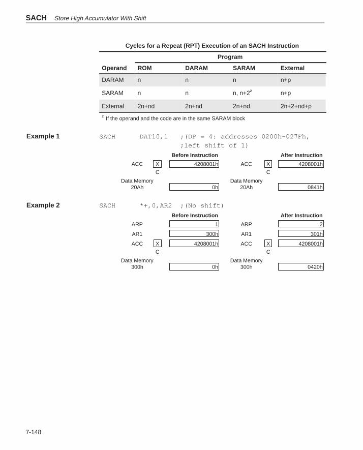
SACH Store High Accumulator With Shift
7-148
Cycles for a Repeat (RPT) Execution of an SACH Instruction
Program
Operand ROM DARAM SARAM External
DARAM n n n n+p
SARAM n n n, n+2† n+p
External 2n+nd 2n+nd 2n+nd 2n+2+nd+p
† If the operand and the code are in the same SARAM block
Example 1 SACH DAT10,1 ;(DP = 4: addresses 0200h–027Fh,;left shift of 1)
Before Instruction After Instruction
ACC X 4208001h ACC X 4208001h
C C
Data Memory Data Memory20Ah 0h 20Ah 0841h
Example 2 SACH *+,0,AR2 ;(No shift)
Before Instruction After Instruction
ARP 1 ARP 2
AR1 300h AR1 301h
ACC X 4208001h ACC X 4208001h
C C
Data Memory Data Memory300h 0h 300h 0420h
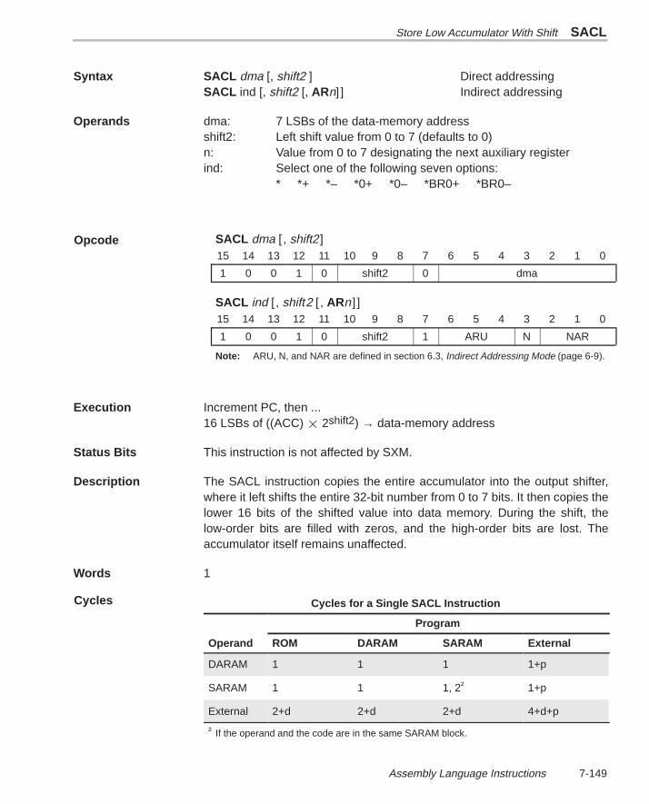
Store Low Accumulator With Shift SACL
7-149 Assembly Language Instructions
Syntax SACL dma [, shift2 ] Direct addressingSACL ind [, shift2 [, ARn]] Indirect addressing
Operands dma: 7 LSBs of the data-memory addressshift2: Left shift value from 0 to 7 (defaults to 0)n: Value from 0 to 7 designating the next auxiliary registerind: Select one of the following seven options:
* *+ *– *0+ *0– *BR0+ *BR0–
SACL dma [ , shift2]15 14 13 12 11 10 9 8 7 6 5 4 3 2 1 0
1 0 0 1 0 shift2 0 dma
SACL ind [, shift2[, ARn]]15 14 13 12 11 10 9 8 7 6 5 4 3 2 1 0
1 0 0 1 0 shift2 1 ARU N NAR
Note: ARU, N, and NAR are defined in section 6.3, Indirect Addressing Mode (page 6-9).
Execution Increment PC, then ...16 LSBs of ((ACC) 2shift2) → data-memory address
Status Bits This instruction is not affected by SXM.
Description The SACL instruction copies the entire accumulator into the output shifter,where it left shifts the entire 32-bit number from 0 to 7 bits. It then copies thelower 16 bits of the shifted value into data memory. During the shift, thelow-order bits are filled with zeros, and the high-order bits are lost. Theaccumulator itself remains unaffected.
Words 1
Cycles for a Single SACL Instruction
Program
Operand ROM DARAM SARAM External
DARAM 1 1 1 1+p
SARAM 1 1 1, 2† 1+p
External 2+d 2+d 2+d 4+d+p
† If the operand and the code are in the same SARAM block.
Opcode
Cycles

SACL Store Low Accumulator With Shift
7-150
Cycles for a Repeat (RPT) Execution of an SACL Instruction
Program
Operand ROM DARAM SARAM External
DARAM n n n n+p
SARAM n n n, n+2† n+p
External 2n+nd 2n+nd 2n+nd 2n+2+nd+p
† If the operand and the code are in the same SARAM block.
Example 1 SACL DAT11,1 ;(DP = 4: addresses 0200h–027Fh,;left shift of 1)
Before Instruction After Instruction
ACC X 7C63 8421 ACC X 7C63 8421h
C C
Data Memory Data Memory20Bh 05h 20Bh 0842h
Example 2 SACL *,0,AR7 ;(No shift)
Before Instruction After Instruction
ARP 6 ARP 7
AR6 300h AR6 300h
ACC X 00FF 8421h ACC X 00FF 8421h
C C
Data Memory Data Memory300h 05h 300h 8421h
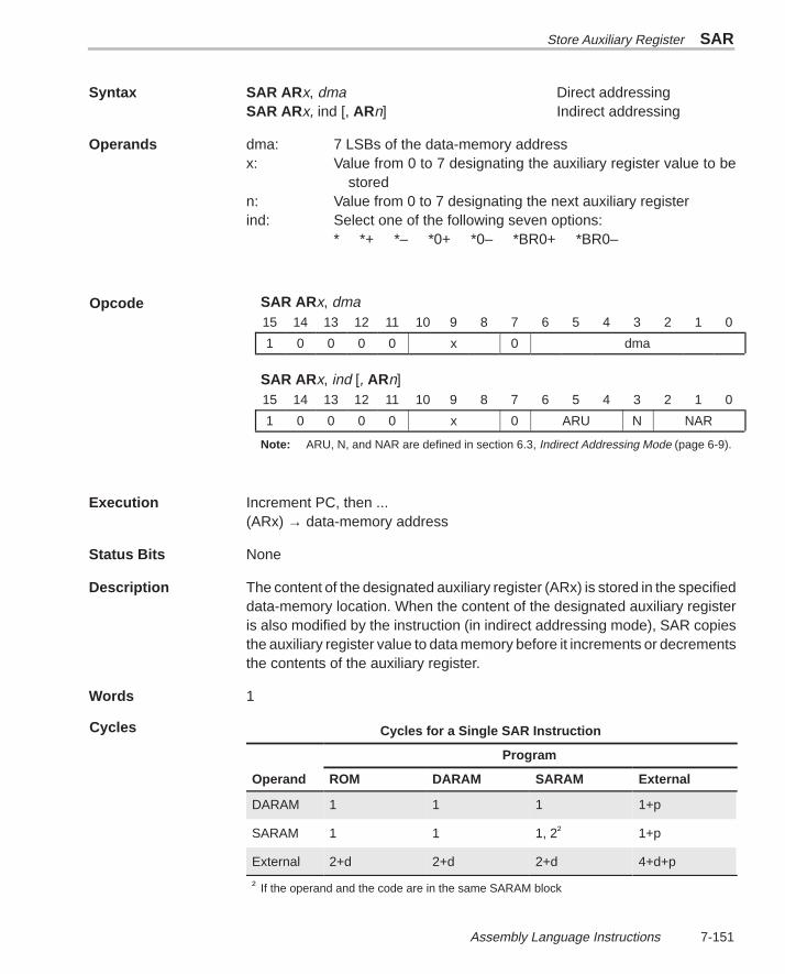
Store Auxiliary Register SAR
7-151 Assembly Language Instructions
Syntax SAR ARx, dma Direct addressingSAR ARx, ind [, ARn] Indirect addressing
Operands dma: 7 LSBs of the data-memory addressx: Value from 0 to 7 designating the auxiliary register value to be
storedn: Value from 0 to 7 designating the next auxiliary registerind: Select one of the following seven options:
* *+ *– *0+ *0– *BR0+ *BR0–
SAR ARx, dma15 14 13 12 11 10 9 8 7 6 5 4 3 2 1 0
1 0 0 0 0 x 0 dma
SAR ARx, ind [, ARn]15 14 13 12 11 10 9 8 7 6 5 4 3 2 1 0
1 0 0 0 0 x 0 ARU N NAR
Note: ARU, N, and NAR are defined in section 6.3, Indirect Addressing Mode (page 6-9).
Execution Increment PC, then ...(ARx) → data-memory address
Status Bits None
Description The content of the designated auxiliary register (ARx) is stored in the specifieddata-memory location. When the content of the designated auxiliary registeris also modified by the instruction (in indirect addressing mode), SAR copiesthe auxiliary register value to data memory before it increments or decrementsthe contents of the auxiliary register.
Words 1
Cycles for a Single SAR Instruction
Program
Operand ROM DARAM SARAM External
DARAM 1 1 1 1+p
SARAM 1 1 1, 2† 1+p
External 2+d 2+d 2+d 4+d+p
† If the operand and the code are in the same SARAM block
Opcode
Cycles
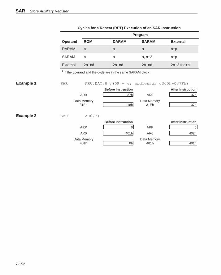
SAR Store Auxiliary Register
7-152
Cycles for a Repeat (RPT) Execution of an SAR Instruction
Program
Operand ROM DARAM SARAM External
DARAM n n n n+p
SARAM n n n, n+2† n+p
External 2n+nd 2n+nd 2n+nd 2n+2+nd+p
† If the operand and the code are in the same SARAM block
Example 1 SAR AR0,DAT30 ;(DP = 6: addresses 0300h–037Fh)
Before Instruction After Instruction
AR0 37h AR0 37h
Data Memory Data Memory31Eh 18h 31Eh 37h
Example 2 SAR AR0,*+
Before Instruction After Instruction
ARP 0 ARP 0
AR0 401h AR0 402h
Data Memory Data Memory401h 0h 401h 401h
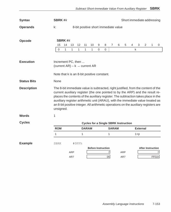
Subtract Short-Immediate Value From Auxiliary Register SBRK
7-153 Assembly Language Instructions
Syntax SBRK #k Short immediate addressing
Operands k: 8-bit positive short immediate value
SBRK #k15 14 13 12 11 10 9 8 7 6 5 4 3 2 1 0
0 1 1 1 1 1 0 0 k
Execution Increment PC, then ...(current AR) – k → current AR
Note that k is an 8-bit positive constant.
Status Bits None
Description The 8-bit immediate value is subtracted, right justified, from the content of thecurrent auxiliary register (the one pointed to by the ARP) and the result re-places the contents of the auxiliary register. The subtraction takes place in theauxiliary register arithmetic unit (ARAU), with the immediate value treated asan 8-bit positive integer. All arithmetic operations on the auxiliary registers areunsigned.
Words 1
Cycles for a Single SBRK Instruction
ROM DARAM SARAM External
1 1 1 1+p
Example SBRK #0FFh
Before Instruction After Instruction
ARP 7 ARP 7
AR7 0h AR7 FF01h
Opcode
Cycles
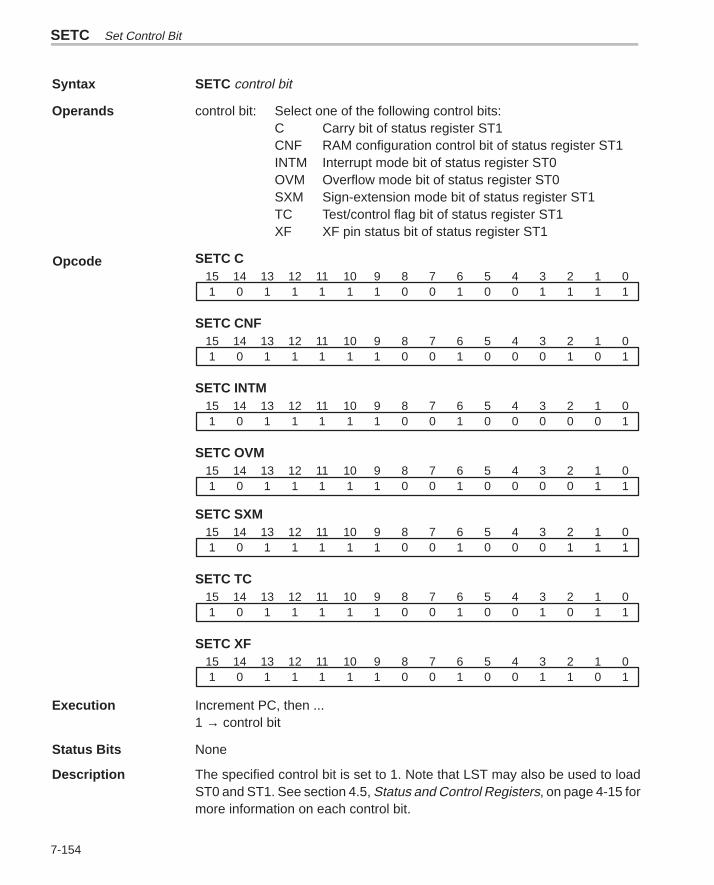
SETC Set Control Bit
7-154
Syntax SETC control bit
Operands control bit: Select one of the following control bits:C Carry bit of status register ST1CNF RAM configuration control bit of status register ST1INTM Interrupt mode bit of status register ST0OVM Overflow mode bit of status register ST0SXM Sign-extension mode bit of status register ST1TC Test/control flag bit of status register ST1XF XF pin status bit of status register ST1
SETC C01234567891011121314151111001001111101
SETC CNF01234567891011121314151010001001111101
SETC INTM01234567891011121314151000001001111101
SETC OVM01234567891011121314151100001001111101
SETC SXM01234567891011121314151110001001111101
SETC TC01234567891011121314151101001001111101
SETC XF01234567891011121314151011001001111101
Execution Increment PC, then ...1 → control bit
Status Bits None
Description The specified control bit is set to 1. Note that LST may also be used to loadST0 and ST1. See section 4.5, Status and Control Registers, on page 4-15 formore information on each control bit.
Opcode
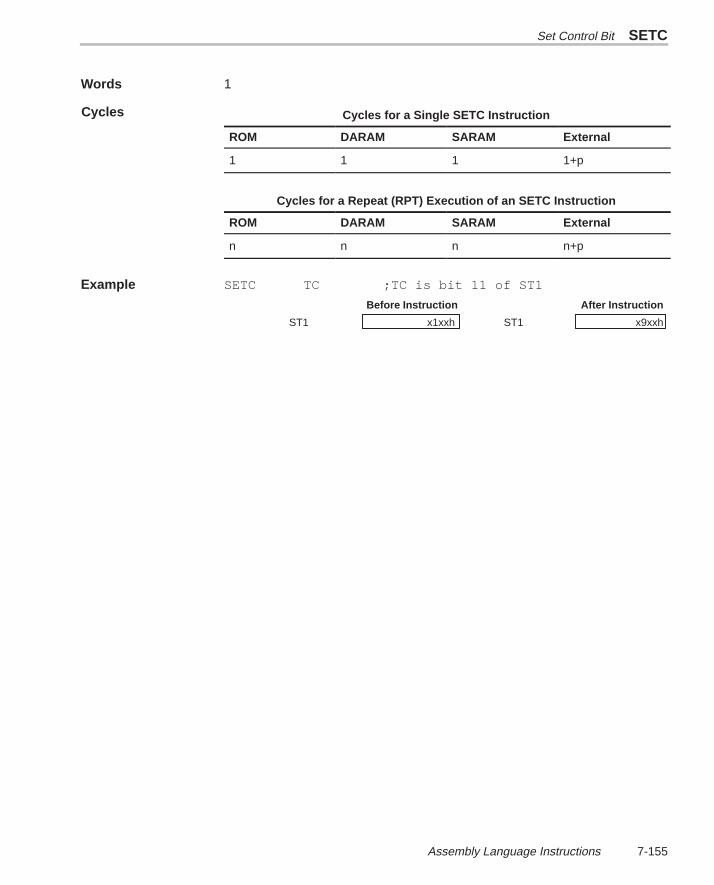
Set Control Bit SETC
7-155 Assembly Language Instructions
Words 1
Cycles for a Single SETC Instruction
ROM DARAM SARAM External
1 1 1 1+p
Cycles for a Repeat (RPT) Execution of an SETC Instruction
ROM DARAM SARAM External
n n n n+p
Example SETC TC ;TC is bit 11 of ST1
Before Instruction After Instruction
ST1 x1xxh ST1 x9xxh
Cycles
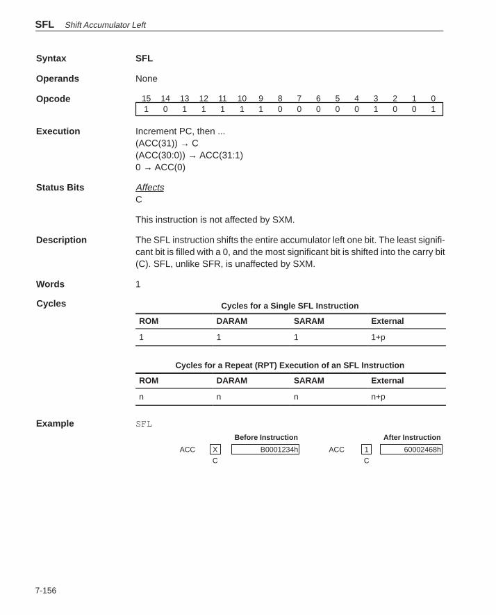
SFL Shift Accumulator Left
7-156
Syntax SFL
Operands None
Opcode 01234567891011121314151001000001111101
Execution Increment PC, then ...(ACC(31)) → C(ACC(30:0)) → ACC(31:1)0 → ACC(0)
Status Bits AffectsC
This instruction is not affected by SXM.
Description The SFL instruction shifts the entire accumulator left one bit. The least signifi-cant bit is filled with a 0, and the most significant bit is shifted into the carry bit(C). SFL, unlike SFR, is unaffected by SXM.
Words 1
Cycles for a Single SFL Instruction
ROM DARAM SARAM External
1 1 1 1+p
Cycles for a Repeat (RPT) Execution of an SFL Instruction
ROM DARAM SARAM External
n n n n+p
Example SFL
Before Instruction After Instruction
ACC X B0001234h ACC 1 60002468h
C C
Cycles
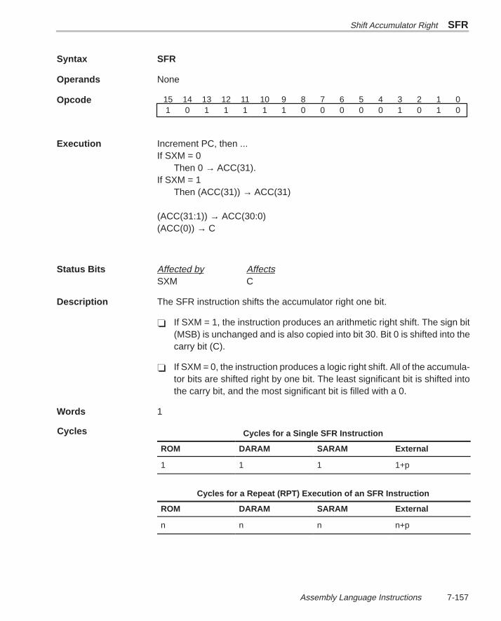
Shift Accumulator Right SFR
7-157 Assembly Language Instructions
Syntax SFR
Operands None
Opcode 01234567891011121314150101000001111101
Execution Increment PC, then ...If SXM = 0
Then 0 → ACC(31).If SXM = 1
Then (ACC(31)) → ACC(31)
(ACC(31:1)) → ACC(30:0) (ACC(0)) → C
Status Bits Affected by AffectsSXM C
Description The SFR instruction shifts the accumulator right one bit.
If SXM = 1, the instruction produces an arithmetic right shift. The sign bit(MSB) is unchanged and is also copied into bit 30. Bit 0 is shifted into thecarry bit (C).
If SXM = 0, the instruction produces a logic right shift. All of the accumula-tor bits are shifted right by one bit. The least significant bit is shifted intothe carry bit, and the most significant bit is filled with a 0.
Words 1
Cycles for a Single SFR Instruction
ROM DARAM SARAM External
1 1 1 1+p
Cycles for a Repeat (RPT) Execution of an SFR Instruction
ROM DARAM SARAM External
n n n n+p
Cycles
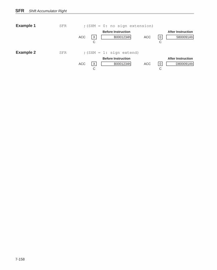
SFR Shift Accumulator Right
7-158
Example 1 SFR ;(SXM = 0: no sign extension)
Before Instruction After Instruction
ACC X B0001234h ACC 0 5800091Ah
C C
Example 2 SFR ;(SXM = 1: sign extend)
Before Instruction After Instruction
ACC X B0001234h ACC 0 D800091Ah
C C
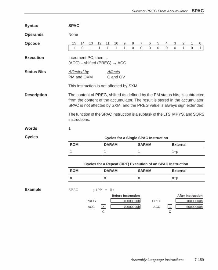
Subtract PREG From Accumulator SPAC
7-159 Assembly Language Instructions
Syntax SPAC
Operands None
Opcode 01234567891011121314151010000001111101
Execution Increment PC, then ...(ACC) – shifted (PREG) → ACC
Status Bits Affected by AffectsPM and OVM C and OV
This instruction is not affected by SXM.
Description The content of PREG, shifted as defined by the PM status bits, is subtractedfrom the content of the accumulator. The result is stored in the accumulator.SPAC is not affected by SXM, and the PREG value is always sign extended.
The function of the SPAC instruction is a subtask of the LTS, MPYS, and SQRSinstructions.
Words 1
Cycles for a Single SPAC Instruction
ROM DARAM SARAM External
1 1 1 1+p
Cycles for a Repeat (RPT) Execution of an SPAC Instruction
ROM DARAM SARAM External
n n n n+p
Example SPAC ;(PM = 0)
Before Instruction After Instruction
PREG 10000000h PREG 10000000h
ACC X 70000000h ACC 1 60000000h
C C
Cycles

SPH Store High PREG
7-160
Syntax SPH dma Direct addressingSPH ind [, ARn] Indirect addressing
Operands dma: 7 LSBs of the data-memory addressn: Value from 0 to 7 designating the next auxiliary registerind: Select one of the following seven options:
* *+ *– *0+ *0– *BR0+ *BR0–
SPH dma15 14 13 12 11 10 9 8 7 6 5 4 3 2 1 0
1 0 0 0 1 1 0 1 0 dma
SPH ind [, ARn]15 14 13 12 11 10 9 8 7 6 5 4 3 2 1 0
1 0 0 0 1 1 0 1 1 ARU N NAR
Note: ARU, N, and NAR are defined in section 6.3, Indirect Addressing Mode (page 6-9).
Execution Increment PC, then ...16 MSBs of shifted (PREG) → data-memory address
Status Bits Affected byPM
Description The 16 high-order bits of the PREG, shifted as specified by the PM bits, arestored in data memory. First, the 32-bit PREG value is copied into the productshifter, where it is shifted as specified by the PM bits. If the right-shift-by-6mode is selected, the high-order bits are sign extended and the low-order bitsare lost. If a left shift is selected, the high-order bits are lost and the low-orderbits are zero filled. If PM = 00, no shift occurs. Then the 16 MSBs of the shiftedvalue are stored in data memory. Neither the PREG value nor the accumulatorvalue is modified by this instruction.
Words 1
Cycles for a Single SPH Instruction
Program
Operand ROM DARAM SARAM External
DARAM 1 1 1 1+p
SARAM 1 1 1, 2† 1+p
External 2+d 2+d 2+d 4+d+p
† If the operand and the code are in the same SARAM block
Opcode
Cycles
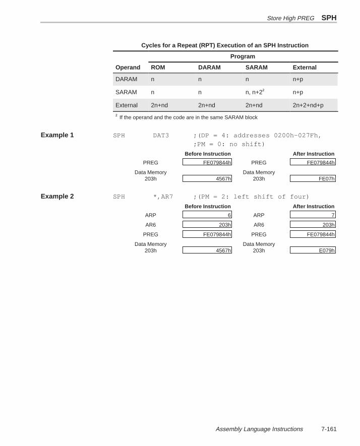
Store High PREG SPH
7-161 Assembly Language Instructions
Cycles for a Repeat (RPT) Execution of an SPH Instruction
Program
Operand ROM DARAM SARAM External
DARAM n n n n+p
SARAM n n n, n+2† n+p
External 2n+nd 2n+nd 2n+nd 2n+2+nd+p
† If the operand and the code are in the same SARAM block
Example 1 SPH DAT3 ;(DP = 4: addresses 0200h–027Fh,;PM = 0: no shift)
Before Instruction After Instruction
PREG FE079844h PREG FE079844h
Data Memory Data Memory203h 4567h 203h FE07h
Example 2 SPH *,AR7 ;(PM = 2: left shift of four)
Before Instruction After Instruction
ARP 6 ARP 7
AR6 203h AR6 203h
PREG FE079844h PREG FE079844h
Data Memory Data Memory203h 4567h 203h E079h
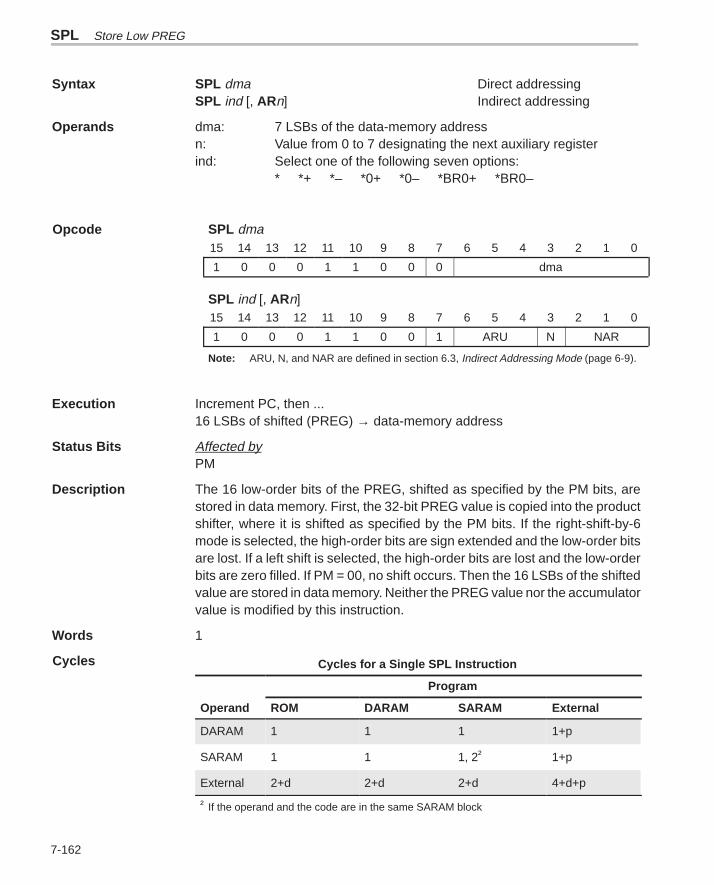
SPL Store Low PREG
7-162
Syntax SPL dma Direct addressingSPL ind [, ARn] Indirect addressing
Operands dma: 7 LSBs of the data-memory addressn: Value from 0 to 7 designating the next auxiliary registerind: Select one of the following seven options:
* *+ *– *0+ *0– *BR0+ *BR0–
SPL dma15 14 13 12 11 10 9 8 7 6 5 4 3 2 1 0
1 0 0 0 1 1 0 0 0 dma
SPL ind [, ARn]15 14 13 12 11 10 9 8 7 6 5 4 3 2 1 0
1 0 0 0 1 1 0 0 1 ARU N NAR
Note: ARU, N, and NAR are defined in section 6.3, Indirect Addressing Mode (page 6-9).
Execution Increment PC, then ...16 LSBs of shifted (PREG) → data-memory address
Status Bits Affected byPM
Description The 16 low-order bits of the PREG, shifted as specified by the PM bits, arestored in data memory. First, the 32-bit PREG value is copied into the productshifter, where it is shifted as specified by the PM bits. If the right-shift-by-6mode is selected, the high-order bits are sign extended and the low-order bitsare lost. If a left shift is selected, the high-order bits are lost and the low-orderbits are zero filled. If PM = 00, no shift occurs. Then the 16 LSBs of the shiftedvalue are stored in data memory. Neither the PREG value nor the accumulatorvalue is modified by this instruction.
Words 1
Cycles for a Single SPL Instruction
Program
Operand ROM DARAM SARAM External
DARAM 1 1 1 1+p
SARAM 1 1 1, 2† 1+p
External 2+d 2+d 2+d 4+d+p
† If the operand and the code are in the same SARAM block
Opcode
Cycles

Store Low PREG SPL
7-163 Assembly Language Instructions
Cycles for a Repeat (RPT) Execution of an SPL Instruction
Program
Operand ROM DARAM SARAM External
DARAM n n n n+p
SARAM n n n, n+2† n+p
External 2n+nd 2n+nd 2n+nd 2n+2+nd+p
† If the operand and the code are in the same SARAM block
Example 1 SPL DAT5 ;(DP = 4: addresses 0200h–027Fh,;PM = 2: left shift of four)
Before Instruction After Instruction
PREG 0FE079844h PREG 0FE079844h
Data Memory Data Memory205h 4567h 205h 08440h
Example 2 SPL *,AR3 ;(PM = 0: no shift)
Before Instruction After Instruction
ARP 2 ARP 3
AR2 205h AR2 205h
PREG 0FE079844h PREG 0FE079844h
Data Memory Data Memory205h 4567h 205h 09844h
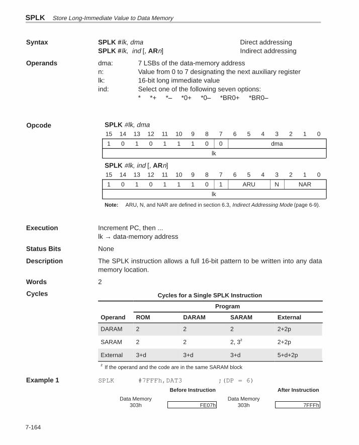
SPLK Store Long-Immediate Value to Data Memory
7-164
Syntax SPLK #lk, dma Direct addressingSPLK #lk, ind [, ARn] Indirect addressing
Operands dma: 7 LSBs of the data-memory addressn: Value from 0 to 7 designating the next auxiliary registerlk: 16-bit long immediate valueind: Select one of the following seven options:
* *+ *– *0+ *0– *BR0+ *BR0–
SPLK #lk, dma15 14 13 12 11 10 9 8 7 6 5 4 3 2 1 0
1 0 1 0 1 1 1 0 0 dma
lk
SPLK #lk, ind [, ARn]15 14 13 12 11 10 9 8 7 6 5 4 3 2 1 0
1 0 1 0 1 1 1 0 1 ARU N NAR
lk
Note: ARU, N, and NAR are defined in section 6.3, Indirect Addressing Mode (page 6-9).
Execution Increment PC, then ...lk → data-memory address
Status Bits None
Description The SPLK instruction allows a full 16-bit pattern to be written into any datamemory location.
Words 2
Cycles for a Single SPLK Instruction
Program
Operand ROM DARAM SARAM External
DARAM 2 2 2 2+2p
SARAM 2 2 2, 3† 2+2p
External 3+d 3+d 3+d 5+d+2p
† If the operand and the code are in the same SARAM block
Example 1 SPLK #7FFFh,DAT3 ;(DP = 6)
Before Instruction After Instruction
Data Memory Data Memory303h FE07h 303h 7FFFh
Opcode
Cycles
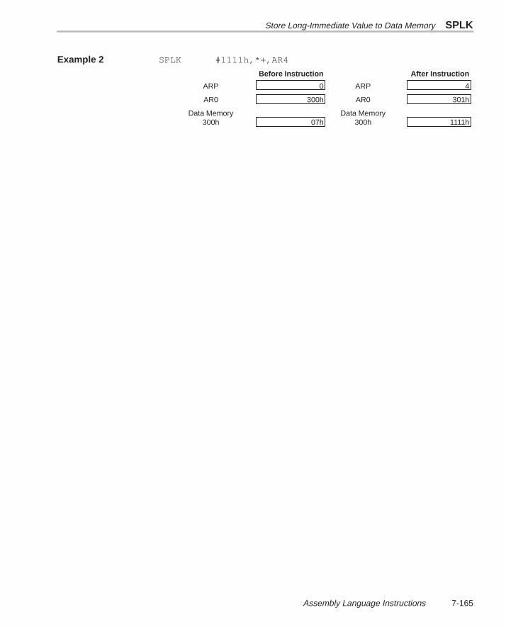
Store Long-Immediate Value to Data Memory SPLK
7-165 Assembly Language Instructions
Example 2 SPLK #1111h,*+,AR4
Before Instruction After Instruction
ARP 0 ARP 4
AR0 300h AR0 301h
Data Memory Data Memory300h 07h 300h 1111h
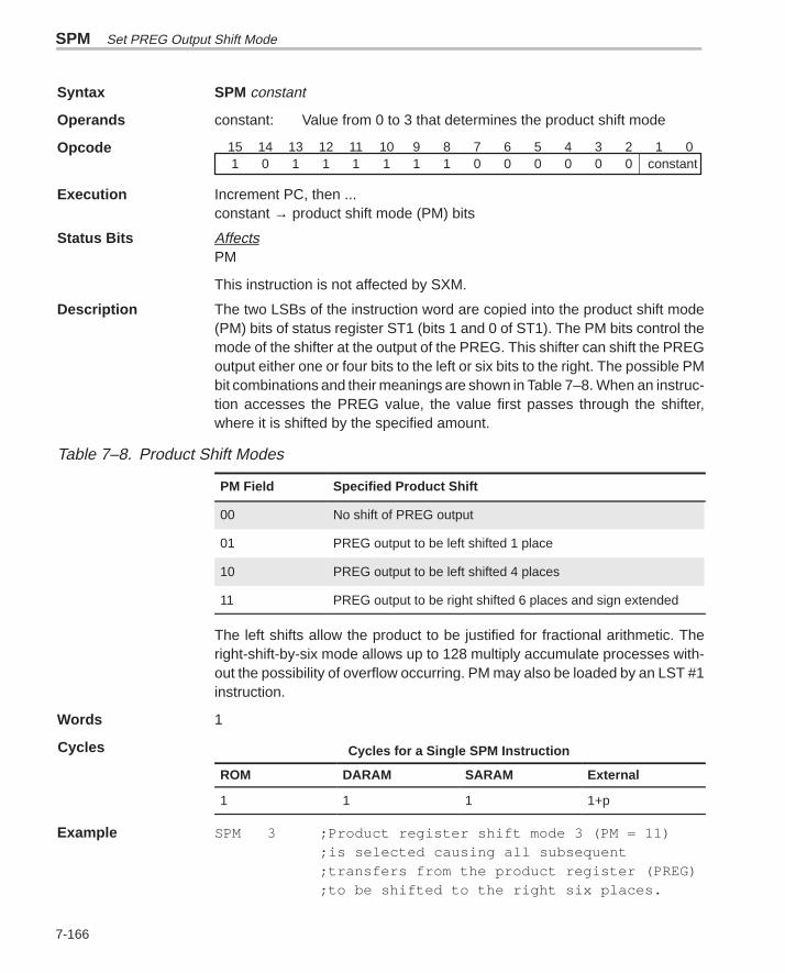
SPM Set PREG Output Shift Mode
7-166
Syntax SPM constant
Operands constant: Value from 0 to 3 that determines the product shift mode
Opcodeconstant00000011111101
0123456789101112131415
Execution Increment PC, then ...constant → product shift mode (PM) bits
Status Bits AffectsPM
This instruction is not affected by SXM.
Description The two LSBs of the instruction word are copied into the product shift mode(PM) bits of status register ST1 (bits 1 and 0 of ST1). The PM bits control themode of the shifter at the output of the PREG. This shifter can shift the PREGoutput either one or four bits to the left or six bits to the right. The possible PMbit combinations and their meanings are shown in Table 7–8. When an instruc-tion accesses the PREG value, the value first passes through the shifter,where it is shifted by the specified amount.
Table 7–8. Product Shift Modes
PM Field Specified Product Shift
00 No shift of PREG output
01 PREG output to be left shifted 1 place
10 PREG output to be left shifted 4 places
11 PREG output to be right shifted 6 places and sign extended
The left shifts allow the product to be justified for fractional arithmetic. Theright-shift-by-six mode allows up to 128 multiply accumulate processes with-out the possibility of overflow occurring. PM may also be loaded by an LST #1instruction.
Words 1
Cycles for a Single SPM Instruction
ROM DARAM SARAM External
1 1 1 1+p
Example SPM 3 ;Product register shift mode 3 (PM = 11);is selected causing all subsequent;transfers from the product register (PREG);to be shifted to the right six places.
Cycles
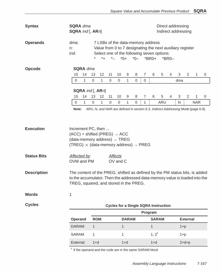
Square Value and Accumulate Previous Product SQRA
7-167 Assembly Language Instructions
Syntax SQRA dma Direct addressingSQRA ind [, ARn] Indirect addressing
Operands dma: 7 LSBs of the data-memory addressn: Value from 0 to 7 designating the next auxiliary registerind: Select one of the following seven options:
* *+ *– *0+ *0– *BR0+ *BR0–
SQRA dma15 14 13 12 11 10 9 8 7 6 5 4 3 2 1 0
0 1 0 1 0 0 1 0 0 dma
SQRA ind [, ARn]15 14 13 12 11 10 9 8 7 6 5 4 3 2 1 0
0 1 0 1 0 0 1 0 1 ARU N NAR
Note: ARU, N, and NAR are defined in section 6.3, Indirect Addressing Mode (page 6-9).
Execution Increment PC, then ...(ACC) + shifted (PREG) → ACC(data-memory address) → TREG(TREG) (data-memory address) → PREG
Status Bits Affected by AffectsOVM and PM OV and C
Description The content of the PREG, shifted as defined by the PM status bits, is addedto the accumulator. Then the addressed data-memory value is loaded into theTREG, squared, and stored in the PREG.
Words 1
Cycles for a Single SQRA Instruction
Program
Operand ROM DARAM SARAM External
DARAM 1 1 1 1+p
SARAM 1 1 1, 2† 1+p
External 1+d 1+d 1+d 2+d+p
† If the operand and the code are in the same SARAM block
Opcode
Cycles
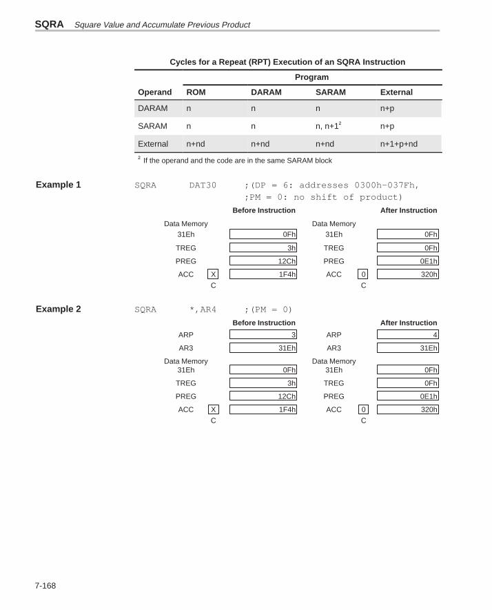
SQRA Square Value and Accumulate Previous Product
7-168
Cycles for a Repeat (RPT) Execution of an SQRA Instruction
Program
Operand ROM DARAM SARAM External
DARAM n n n n+p
SARAM n n n, n+1† n+p
External n+nd n+nd n+nd n+1+p+nd
† If the operand and the code are in the same SARAM block
Example 1 SQRA DAT30 ;(DP = 6: addresses 0300h–037Fh,;PM = 0: no shift of product)
Before Instruction After Instruction
Data Memory Data Memory
31Eh 0Fh 31Eh 0Fh
TREG 3h TREG 0Fh
PREG 12Ch PREG 0E1h
ACC X 1F4h ACC 0 320h
C C
Example 2 SQRA *,AR4 ;(PM = 0)
Before Instruction After Instruction
ARP 3 ARP 4
AR3 31Eh AR3 31Eh
Data Memory Data Memory31Eh 0Fh 31Eh 0Fh
TREG 3h TREG 0Fh
PREG 12Ch PREG 0E1h
ACC X 1F4h ACC 0 320h
C C
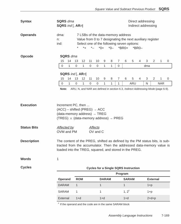
Square Value and Subtract Previous Product SQRS
7-169 Assembly Language Instructions
Syntax SQRS dma Direct addressingSQRS ind [, ARn] Indirect addressing
Operands dma: 7 LSBs of the data-memory addressn: Value from 0 to 7 designating the next auxiliary registerind: Select one of the following seven options:
* *+ *– *0+ *0– *BR0+ *BR0–
SQRS dma15 14 13 12 11 10 9 8 7 6 5 4 3 2 1 0
0 1 0 1 0 0 1 1 0 dma
SQRS ind [, ARn]15 14 13 12 11 10 9 8 7 6 5 4 3 2 1 0
0 1 0 1 0 0 1 1 1 ARU N NAR
Note: ARU, N, and NAR are defined in section 6.3, Indirect Addressing Mode (page 6-9).
Execution Increment PC, then ...(ACC) – shifted (PREG) → ACC(data-memory address) → TREG(TREG) (data-memory address) → PREG
Status Bits Affected by AffectsOVM and PM OV and C
Description The content of the PREG, shifted as defined by the PM status bits, is sub-tracted from the accumulator. Then the addressed data-memory value isloaded into the TREG, squared, and stored in the PREG.
Words 1
Cycles for a Single SQRS Instruction
Program
Operand ROM DARAM SARAM External
DARAM 1 1 1 1+p
SARAM 1 1 1, 2† 1+p
External 1+d 1+d 1+d 2+d+p
† If the operand and the code are in the same SARAM block
Opcode
Cycles
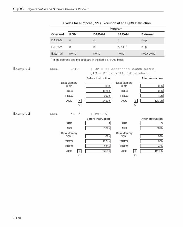
SQRS Square Value and Subtract Previous Product
7-170
Cycles for a Repeat (RPT) Execution of an SQRS Instruction
Program
Operand ROM DARAM SARAM External
DARAM n n n n+p
SARAM n n n, n+1† n+p
External n+nd n+nd n+nd n+1+p+nd
† If the operand and the code are in the same SARAM block
Example 1 SQRS DAT9 ;(DP = 6: addresses 0300h–037Fh,;PM = 0: no shift of product)
Before Instruction After Instruction
Data Memory Data Memory309h 08h 309h 08h
TREG 1124h TREG 08h
PREG 190h PREG 40h
ACC X 1450h ACC 1 12C0h
C C
Example 2 SQRS *,AR5 ;(PM = 0)
Before Instruction After Instruction
ARP 3 ARP 5
AR3 309h AR3 309h
Data Memory Data Memory309h 08h 309h 08h
TREG 1124h TREG 08h
PREG 190h PREG 40h
ACC X 1450h ACC 1 12C0h
C C
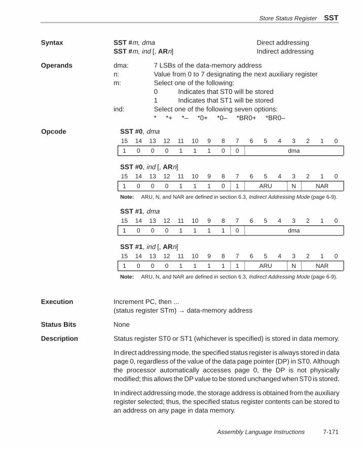
Store Status Register SST
7-171 Assembly Language Instructions
Syntax SST #m, dma Direct addressingSST #m, ind [, ARn] Indirect addressing
Operands dma: 7 LSBs of the data-memory addressn: Value from 0 to 7 designating the next auxiliary registerm: Select one of the following:
0 Indicates that ST0 will be stored1 Indicates that ST1 will be stored
ind: Select one of the following seven options:* *+ *– *0+ *0– *BR0+ *BR0–
SST #0, dma15 14 13 12 11 10 9 8 7 6 5 4 3 2 1 0
1 0 0 0 1 1 1 0 0 dma
SST #0, ind [, ARn]15 14 13 12 11 10 9 8 7 6 5 4 3 2 1 0
1 0 0 0 1 1 1 0 1 ARU N NAR
Note: ARU, N, and NAR are defined in section 6.3, Indirect Addressing Mode (page 6-9).
SST #1, dma15 14 13 12 11 10 9 8 7 6 5 4 3 2 1 0
1 0 0 0 1 1 1 1 0 dma
SST #1, ind [, ARn]15 14 13 12 11 10 9 8 7 6 5 4 3 2 1 0
1 0 0 0 1 1 1 1 1 ARU N NAR
Note: ARU, N, and NAR are defined in section 6.3, Indirect Addressing Mode (page 6-9).
Execution Increment PC, then ...(status register STm) → data-memory address
Status Bits None
Description Status register ST0 or ST1 (whichever is specified) is stored in data memory.
In direct addressing mode, the specified status register is always stored in datapage 0, regardless of the value of the data page pointer (DP) in ST0. Althoughthe processor automatically accesses page 0, the DP is not physicallymodified; this allows the DP value to be stored unchanged when ST0 is stored.
In indirect addressing mode, the storage address is obtained from the auxiliaryregister selected; thus, the specified status register contents can be stored toan address on any page in data memory.
Opcode
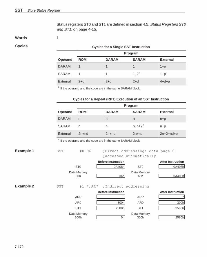
SST Store Status Register
7-172
Status registers ST0 and ST1 are defined in section 4.5, Status Registers ST0and ST1, on page 4-15.
Words 1
Cycles for a Single SST Instruction
Program
Operand ROM DARAM SARAM External
DARAM 1 1 1 1+p
SARAM 1 1 1, 2† 1+p
External 2+d 2+d 2+d 4+d+p
† If the operand and the code are in the same SARAM block
Cycles for a Repeat (RPT) Execution of an SST Instruction
Program
Operand ROM DARAM SARAM External
DARAM n n n n+p
SARAM n n n, n+2† n+p
External 2n+nd 2n+nd 2n+nd 2n+2+nd+p
† If the operand and the code are in the same SARAM block
Example 1 SST #0,96 ;Direct addressing: data page 0;accessed automatically
Before Instruction After Instruction
ST0 0A408h ST0 0A408h
Data Memory Data Memory60h 0Ah 60h 0A408h
Example 2 SST #1,*,AR7 ;Indirect addressing
Before Instruction After Instruction
ARP 0 ARP 7
AR0 300h AR0 300h
ST1 2580h ST1 2580h
Data Memory Data Memory300h 0h 300h 2580h
Cycles
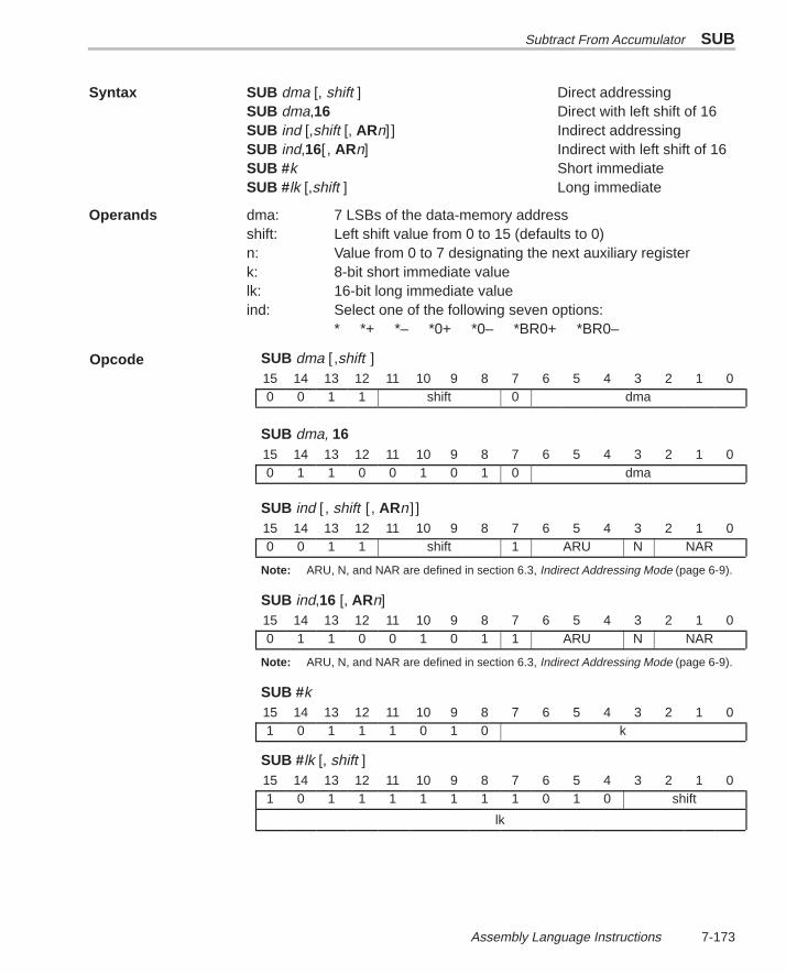
Subtract From Accumulator SUB
7-173 Assembly Language Instructions
Syntax SUB dma [, shift ] Direct addressingSUB dma,16 Direct with left shift of 16SUB ind [,shift [, ARn]] Indirect addressingSUB ind,16[ , ARn] Indirect with left shift of 16SUB #k Short immediateSUB #lk [,shift ] Long immediate
Operands dma: 7 LSBs of the data-memory addressshift: Left shift value from 0 to 15 (defaults to 0)n: Value from 0 to 7 designating the next auxiliary registerk: 8-bit short immediate valuelk: 16-bit long immediate valueind: Select one of the following seven options:
* *+ *– *0+ *0– *BR0+ *BR0–
SUB dma [ ,shift ]15 14 13 12 11 10 9 8 7 6 5 4 3 2 1 00 0 1 1 shift 0 dma
SUB dma, 1615 14 13 12 11 10 9 8 7 6 5 4 3 2 1 00 1 1 0 0 1 0 1 0 dma
SUB ind [, shift [, ARn]]15 14 13 12 11 10 9 8 7 6 5 4 3 2 1 00 0 1 1 shift 1 ARU N NAR
Note: ARU, N, and NAR are defined in section 6.3, Indirect Addressing Mode (page 6-9).
SUB ind,16 [, ARn]15 14 13 12 11 10 9 8 7 6 5 4 3 2 1 00 1 1 0 0 1 0 1 1 ARU N NAR
Note: ARU, N, and NAR are defined in section 6.3, Indirect Addressing Mode (page 6-9).
SUB #k15 14 13 12 11 10 9 8 7 6 5 4 3 2 1 01 0 1 1 1 0 1 0 k
SUB #lk [, shift ]15 14 13 12 11 10 9 8 7 6 5 4 3 2 1 01 0 1 1 1 1 1 1 1 0 1 0 shift
lk
Opcode
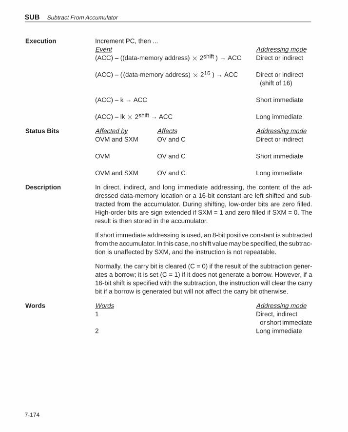
SUB Subtract From Accumulator
7-174
Execution Increment PC, then ...Event Addressing mode(ACC) – ((data-memory address) 2shift ) → ACC Direct or indirect
(ACC) – ((data-memory address) 216 ) → ACC Direct or indirect(shift of 16)
(ACC) – k → ACC Short immediate
(ACC) – lk 2shift → ACC Long immediate
Status Bits Affected by Affects Addressing modeOVM and SXM OV and C Direct or indirect
OVM OV and C Short immediate
OVM and SXM OV and C Long immediate
Description In direct, indirect, and long immediate addressing, the content of the ad-dressed data-memory location or a 16-bit constant are left shifted and sub-tracted from the accumulator. During shifting, low-order bits are zero filled.High-order bits are sign extended if SXM = 1 and zero filled if SXM = 0. Theresult is then stored in the accumulator.
If short immediate addressing is used, an 8-bit positive constant is subtractedfrom the accumulator. In this case, no shift value may be specified, the subtrac-tion is unaffected by SXM, and the instruction is not repeatable.
Normally, the carry bit is cleared (C = 0) if the result of the subtraction gener-ates a borrow; it is set (C = 1) if it does not generate a borrow. However, if a16-bit shift is specified with the subtraction, the instruction will clear the carrybit if a borrow is generated but will not affect the carry bit otherwise.
Words Words Addressing mode1 Direct, indirect
or short immediate2 Long immediate
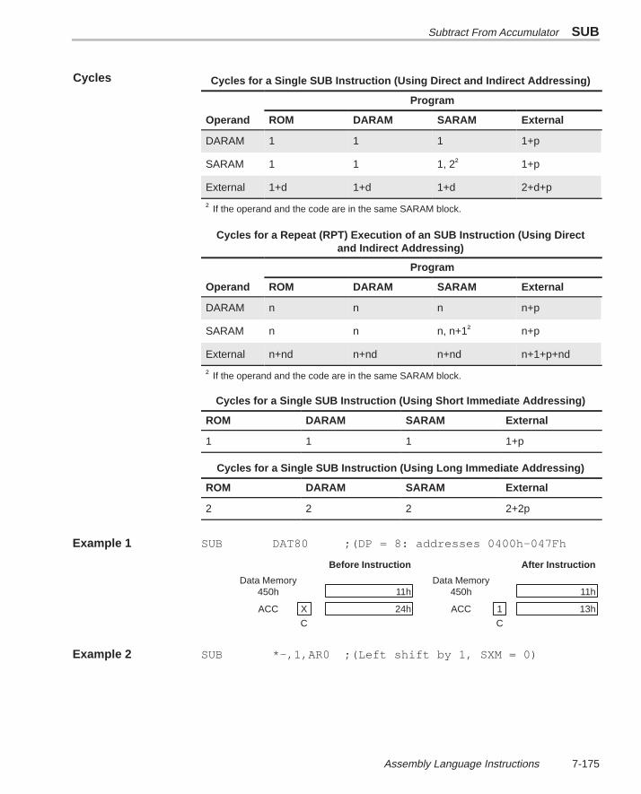
Subtract From Accumulator SUB
7-175 Assembly Language Instructions
Cycles for a Single SUB Instruction (Using Direct and Indirect Addressing)
Program
Operand ROM DARAM SARAM External
DARAM 1 1 1 1+p
SARAM 1 1 1, 2† 1+p
External 1+d 1+d 1+d 2+d+p
† If the operand and the code are in the same SARAM block.
Cycles for a Repeat (RPT) Execution of an SUB Instruction (Using Directand Indirect Addressing)
Program
Operand ROM DARAM SARAM External
DARAM n n n n+p
SARAM n n n, n+1† n+p
External n+nd n+nd n+nd n+1+p+nd
† If the operand and the code are in the same SARAM block.
Cycles for a Single SUB Instruction (Using Short Immediate Addressing)
ROM DARAM SARAM External
1 1 1 1+p
Cycles for a Single SUB Instruction (Using Long Immediate Addressing)
ROM DARAM SARAM External
2 2 2 2+2p
Example 1 SUB DAT80 ;(DP = 8: addresses 0400h–047Fh
Before Instruction After Instruction
Data Memory Data Memory450h 11h 450h 11h
ACC X 24h ACC 1 13h
C C
Example 2 SUB *–,1,AR0 ;(Left shift by 1, SXM = 0)
Cycles
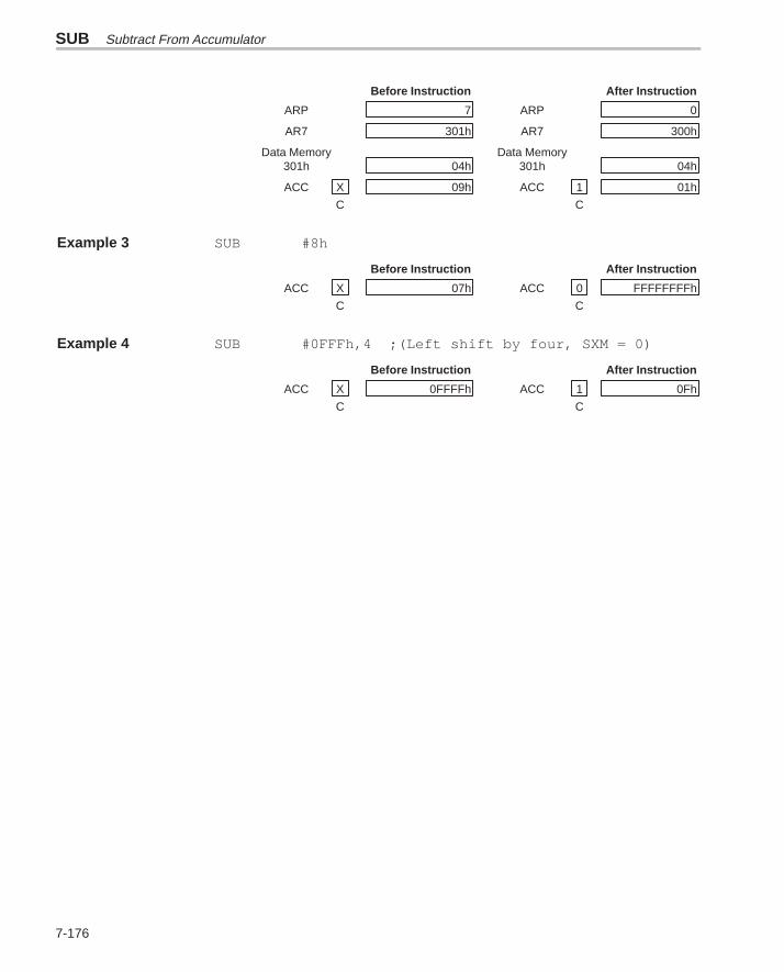
SUB Subtract From Accumulator
7-176
Before Instruction After Instruction
ARP 7 ARP 0
AR7 301h AR7 300h
Data Memory Data Memory301h 04h 301h 04h
ACC X 09h ACC 1 01h
C C
Example 3 SUB #8h
Before Instruction After Instruction
ACC X 07h ACC 0 FFFFFFFFh
C C
Example 4 SUB #0FFFh,4 ;(Left shift by four, SXM = 0)
Before Instruction After Instruction
ACC X 0FFFFh ACC 1 0Fh
C C
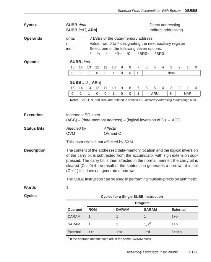
Subtract From Accumulator With Borrow SUBB
7-177 Assembly Language Instructions
Syntax SUBB dma Direct addressingSUBB ind [, ARn] Indirect addressing
Operands dma: 7 LSBs of the data-memory addressn: Value from 0 to 7 designating the next auxiliary registerind: Select one of the following seven options:
* *+ *– *0+ *0– *BR0+ *BR0–
SUBB dma15 14 13 12 11 10 9 8 7 6 5 4 3 2 1 0
0 1 1 0 0 1 0 0 0 dma
SUBB ind [, ARn]15 14 13 12 11 10 9 8 7 6 5 4 3 2 1 0
0 1 1 0 0 1 0 0 1 ARU N NAR
Note: ARU, N, and NAR are defined in section 6.3, Indirect Addressing Mode (page 6-9).
Execution Increment PC, then ...(ACC) – (data-memory address) – (logical inversion of C) → ACC
Status Bits Affected by AffectsOVM OV and C
This instruction is not affected by SXM.
Description The content of the addressed data-memory location and the logical inversionof the carry bit is subtracted from the accumulator with sign extension sup-pressed. The carry bit is then affected in the normal manner: the carry bit iscleared (C = 0) if the result of the subtraction generates a borrow; it is set(C = 1) if it does not generate a borrow.
The SUBB instruction can be used in performing multiple-precision arithmetic.
Words 1
Cycles for a Single SUBB Instruction
Program
Operand ROM DARAM SARAM External
DARAM 1 1 1 1+p
SARAM 1 1 1, 2† 1+p
External 1+d 1+d 1+d 2+d+p
† If the operand and the code are in the same SARAM block
Opcode
Cycles
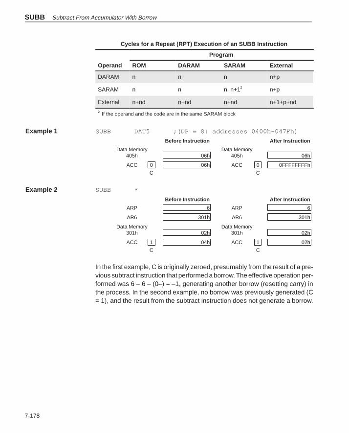
SUBB Subtract From Accumulator With Borrow
7-178
Cycles for a Repeat (RPT) Execution of an SUBB Instruction
Program
Operand ROM DARAM SARAM External
DARAM n n n n+p
SARAM n n n, n+1† n+p
External n+nd n+nd n+nd n+1+p+nd
† If the operand and the code are in the same SARAM block
Example 1 SUBB DAT5 ;(DP = 8: addresses 0400h–047Fh)
Before Instruction After Instruction
Data Memory Data Memory405h 06h 405h 06h
ACC 0 06h ACC 0 0FFFFFFFFh
C C
Example 2 SUBB *
Before Instruction After Instruction
ARP 6 ARP 6
AR6 301h AR6 301h
Data Memory Data Memory301h 02h 301h 02h
ACC 1 04h ACC 1 02h
C C
In the first example, C is originally zeroed, presumably from the result of a pre-vious subtract instruction that performed a borrow. The effective operation per-formed was 6 – 6 – (0–) = –1, generating another borrow (resetting carry) inthe process. In the second example, no borrow was previously generated (C= 1), and the result from the subtract instruction does not generate a borrow.
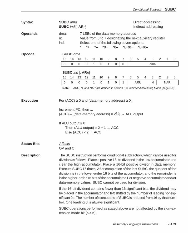
Conditional Subtract SUBC
7-179 Assembly Language Instructions
Syntax SUBC dma Direct addressingSUBC ind [, ARn] Indirect addressing
Operands dma: 7 LSBs of the data-memory addressn: Value from 0 to 7 designating the next auxiliary registerind: Select one of the following seven options:
* *+ *– *0+ *0– *BR0+ *BR0–
SUBC dma15 14 13 12 11 10 9 8 7 6 5 4 3 2 1 0
0 0 0 0 1 0 1 0 0 dma
SUBC ind [, ARn]15 14 13 12 11 10 9 8 7 6 5 4 3 2 1 0
0 0 0 0 1 0 1 0 1 ARU N NAR
Note: ARU, N, and NAR are defined in section 6.3, Indirect Addressing Mode (page 6-9).
Execution For (ACC) ≥ 0 and (data-memory address) ≥ 0:
Increment PC, then ...(ACC) – [(data-memory address) × 215] → ALU output
If ALU output ≥ 0Then (ALU output) × 2 + 1 → ACCElse (ACC) × 2 → ACC
Status Bits AffectsOV and C
Description The SUBC instruction performs conditional subtraction, which can be used fordivision as follows: Place a positive 16-bit dividend in the low accumulator andclear the high accumulator. Place a 16-bit positive divisor in data memory.Execute SUBC 16 times. After completion of the last SUBC, the quotient of thedivision is in the lower-order 16 bits of the accumulator, and the remainder isin the higher-order 16 bits of the accumulator. For negative accumulator and/ordata-memory values, SUBC cannot be used for division.
If the 16-bit dividend contains fewer than 16 significant bits, the dividend maybe placed in the accumulator and left shifted by the number of leading nonsig-nificant 0s. The number of executions of SUBC is reduced from 16 by that num-ber. One leading 0 is always significant.
SUBC operations performed as stated above are not affected by the sign-ex-tension mode bit (SXM).
Opcode
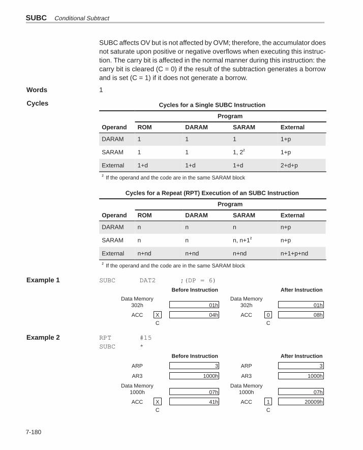
SUBC Conditional Subtract
7-180
SUBC affects OV but is not affected by OVM; therefore, the accumulator doesnot saturate upon positive or negative overflows when executing this instruc-tion. The carry bit is affected in the normal manner during this instruction: thecarry bit is cleared (C = 0) if the result of the subtraction generates a borrowand is set (C = 1) if it does not generate a borrow.
Words 1
Cycles for a Single SUBC Instruction
Program
Operand ROM DARAM SARAM External
DARAM 1 1 1 1+p
SARAM 1 1 1, 2† 1+p
External 1+d 1+d 1+d 2+d+p
† If the operand and the code are in the same SARAM block
Cycles for a Repeat (RPT) Execution of an SUBC Instruction
Program
Operand ROM DARAM SARAM External
DARAM n n n n+p
SARAM n n n, n+1† n+p
External n+nd n+nd n+nd n+1+p+nd
† If the operand and the code are in the same SARAM block
Example 1 SUBC DAT2 ;(DP = 6)
Before Instruction After Instruction
Data Memory Data Memory302h 01h 302h 01h
ACC X 04h ACC 0 08h
C C
Example 2 RPT #15SUBC *
Before Instruction After Instruction
ARP 3 ARP 3
AR3 1000h AR3 1000h
Data Memory Data Memory1000h 07h 1000h 07h
ACC X 41h ACC 1 20009h
C C
Cycles
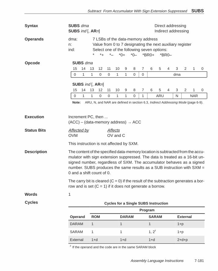
Subtract From Accumulator With Sign Extension Suppressed SUBS
7-181 Assembly Language Instructions
Syntax SUBS dma Direct addressingSUBS ind [, ARn] Indirect addressing
Operands dma: 7 LSBs of the data-memory addressn: Value from 0 to 7 designating the next auxiliary registerind: Select one of the following seven options:
* *+ *– *0+ *0– *BR0+ *BR0–
SUBS dma15 14 13 12 11 10 9 8 7 6 5 4 3 2 1 0
0 1 1 0 0 1 1 0 0 dma
SUBS ind [, ARn]15 14 13 12 11 10 9 8 7 6 5 4 3 2 1 0
0 1 1 0 0 1 1 0 1 ARU N NAR
Note: ARU, N, and NAR are defined in section 6.3, Indirect Addressing Mode (page 6-9).
Execution Increment PC, then ...(ACC) – (data-memory address) → ACC
Status Bits Affected by AffectsOVM OV and C
This instruction is not affected by SXM.
Description The content of the specified data-memory location is subtracted from the accu-mulator with sign extension suppressed. The data is treated as a 16-bit un-signed number, regardless of SXM. The accumulator behaves as a signednumber. SUBS produces the same results as a SUB instruction with SXM =0 and a shift count of 0.
The carry bit is cleared (C = 0) if the result of the subtraction generates a bor-row and is set (C = 1) if it does not generate a borrow.
Words 1
Cycles for a Single SUBS Instruction
Program
Operand ROM DARAM SARAM External
DARAM 1 1 1 1+p
SARAM 1 1 1, 2† 1+p
External 1+d 1+d 1+d 2+d+p
† If the operand and the code are in the same SARAM block
Opcode
Cycles
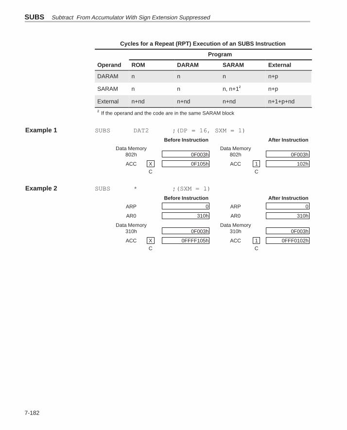
SUBS Subtract From Accumulator With Sign Extension Suppressed
7-182
Cycles for a Repeat (RPT) Execution of an SUBS Instruction
Program
Operand ROM DARAM SARAM External
DARAM n n n n+p
SARAM n n n, n+1† n+p
External n+nd n+nd n+nd n+1+p+nd
† If the operand and the code are in the same SARAM block
Example 1 SUBS DAT2 ;(DP = 16, SXM = 1)
Before Instruction After Instruction
Data Memory Data Memory802h 0F003h 802h 0F003h
ACC X 0F105h ACC 1 102h
C C
Example 2 SUBS * ;(SXM = 1)
Before Instruction After Instruction
ARP 0 ARP 0
AR0 310h AR0 310h
Data Memory Data Memory310h 0F003h 310h 0F003h
ACC X 0FFFF105h ACC 1 0FFF0102h
C C
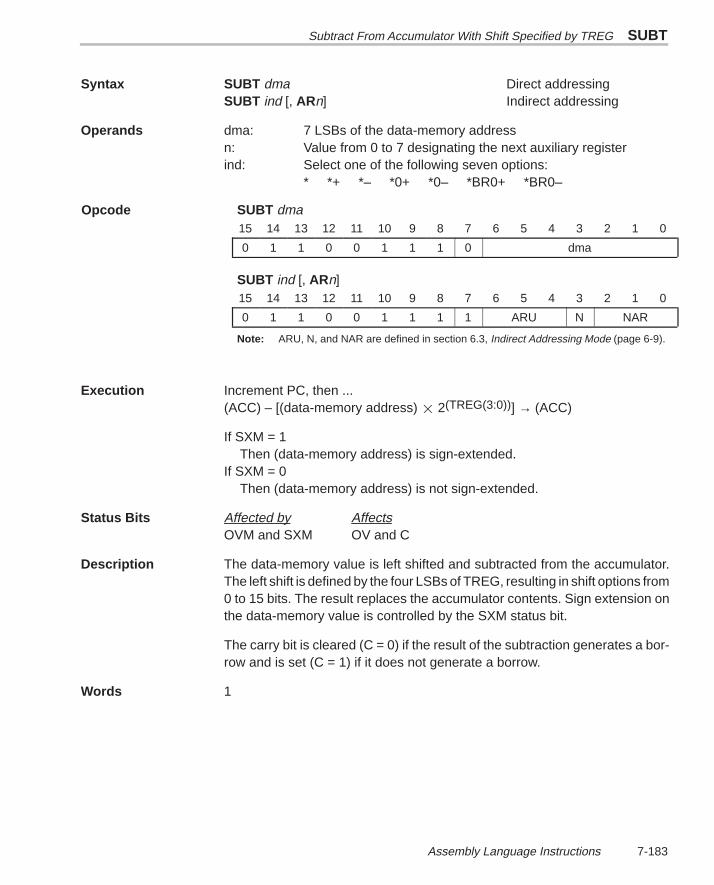
Subtract From Accumulator With Shift Specified by TREG SUBT
7-183 Assembly Language Instructions
Syntax SUBT dma Direct addressingSUBT ind [, ARn] Indirect addressing
Operands dma: 7 LSBs of the data-memory addressn: Value from 0 to 7 designating the next auxiliary registerind: Select one of the following seven options:
* *+ *– *0+ *0– *BR0+ *BR0–
SUBT dma15 14 13 12 11 10 9 8 7 6 5 4 3 2 1 0
0 1 1 0 0 1 1 1 0 dma
SUBT ind [, ARn]15 14 13 12 11 10 9 8 7 6 5 4 3 2 1 0
0 1 1 0 0 1 1 1 1 ARU N NAR
Note: ARU, N, and NAR are defined in section 6.3, Indirect Addressing Mode (page 6-9).
Execution Increment PC, then ...(ACC) – [(data-memory address) 2(TREG(3:0))] → (ACC)
If SXM = 1Then (data-memory address) is sign-extended.
If SXM = 0Then (data-memory address) is not sign-extended.
Status Bits Affected by AffectsOVM and SXM OV and C
Description The data-memory value is left shifted and subtracted from the accumulator.The left shift is defined by the four LSBs of TREG, resulting in shift options from0 to 15 bits. The result replaces the accumulator contents. Sign extension onthe data-memory value is controlled by the SXM status bit.
The carry bit is cleared (C = 0) if the result of the subtraction generates a bor-row and is set (C = 1) if it does not generate a borrow.
Words 1
Opcode
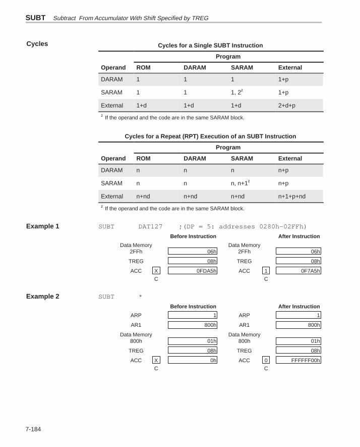
SUBT Subtract From Accumulator With Shift Specified by TREG
7-184
Cycles for a Single SUBT Instruction
Program
Operand ROM DARAM SARAM External
DARAM 1 1 1 1+p
SARAM 1 1 1, 2† 1+p
External 1+d 1+d 1+d 2+d+p
† If the operand and the code are in the same SARAM block.
Cycles for a Repeat (RPT) Execution of an SUBT Instruction
Program
Operand ROM DARAM SARAM External
DARAM n n n n+p
SARAM n n n, n+1† n+p
External n+nd n+nd n+nd n+1+p+nd
† If the operand and the code are in the same SARAM block.
Example 1 SUBT DAT127 ;(DP = 5: addresses 0280h–02FFh)
Before Instruction After Instruction
Data Memory Data Memory2FFh 06h 2FFh 06h
TREG 08h TREG 08h
ACC X 0FDA5h ACC 1 0F7A5h
C C
Example 2 SUBT *
Before Instruction After Instruction
ARP 1 ARP 1
AR1 800h AR1 800h
Data Memory Data Memory800h 01h 800h 01h
TREG 08h TREG 08h
ACC X 0h ACC 0 FFFFFF00h
C C
Cycles
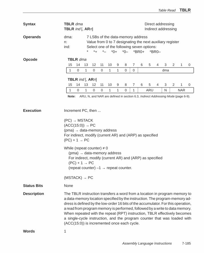
Table Read TBLR
7-185 Assembly Language Instructions
Syntax TBLR dma Direct addressingTBLR ind [, ARn] Indirect addressing
Operands dma: 7 LSBs of the data-memory addressn: Value from 0 to 7 designating the next auxiliary registerind: Select one of the following seven options:
* *+ *– *0+ *0– *BR0+ *BR0–
TBLR dma15 14 13 12 11 10 9 8 7 6 5 4 3 2 1 0
1 0 1 0 0 1 1 0 0 dma
TBLR ind [, ARn]15 14 13 12 11 10 9 8 7 6 5 4 3 2 1 0
1 0 1 0 0 1 1 0 1 ARU N NAR
Note: ARU, N, and NAR are defined in section 6.3, Indirect Addressing Mode (page 6-9).
Execution Increment PC, then ...
(PC) → MSTACK(ACC(15:0)) → PC(pma) → data-memory addressFor indirect, modify (current AR) and (ARP) as specified(PC) + 1 → PC
While (repeat counter) ≠ 0(pma) → data-memory addressFor indirect, modify (current AR) and (ARP) as specified(PC) + 1 → PC(repeat counter) –1 → repeat counter.
(MSTACK) → PC
Status Bits None
Description The TBLR instruction transfers a word from a location in program memory toa data-memory location specified by the instruction. The program-memory ad-dress is defined by the low-order 16 bits of the accumulator. For this operation,a read from program memory is performed, followed by a write to data memory.When repeated with the repeat (RPT) instruction, TBLR effectively becomesa single-cycle instruction, and the program counter that was loaded with(ACC(15:0)) is incremented once each cycle.
Words 1
Opcode
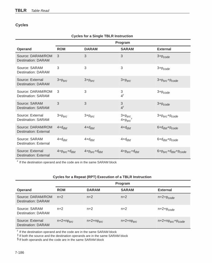
TBLR Table Read
7-186
Cycles
Cycles for a Single TBLR Instruction
Program
Operand ROM DARAM SARAM External
Source: DARAM/ROMDestination: DARAM
3 3 3 3+pcode
Source: SARAMDestination: DARAM
3 3 3 3+pcode
Source: ExternalDestination: DARAM
3+psrc 3+psrc 3+psrc 3+psrc+pcode
Source: DARAM/ROMDestination: SARAM
3 3 34†
3+pcode
Source: SARAMDestination: SARAM
3 3 34†
3+pcode
Source: ExternalDestination: SARAM
3+psrc 3+psrc 3+psrc4+psrc†
3+psrc+pcode
Source: DARAM/ROMDestination: External
4+ddst 4+ddst 4+ddst 6+ddst+pcode
Source: SARAMDestination: External
4+ddst 4+ddst 4+ddst 6+ddst+pcode
Source: ExternalDestination: External
4+psrc+ddst 4+psrc+ddst 4+psrc+ddst 6+psrc+ddst+pcode
† If the destination operand and the code are in the same SARAM block
Cycles for a Repeat (RPT) Execution of a TBLR Instruction
Program
Operand ROM DARAM SARAM External
Source: DARAM/ROMDestination: DARAM
n+2 n+2 n+2 n+2+pcode
Source: SARAMDestination: DARAM
n+2 n+2 n+2 n+2+pcode
Source: ExternalDestination: DARAM
n+2+npsrc n+2+npsrc n+2+npsrc n+2+npsrc+pcode
† If the destination operand and the code are in the same SARAM block‡ If both the source and the destination operands are in the same SARAM block§ If both operands and the code are in the same SARAM block
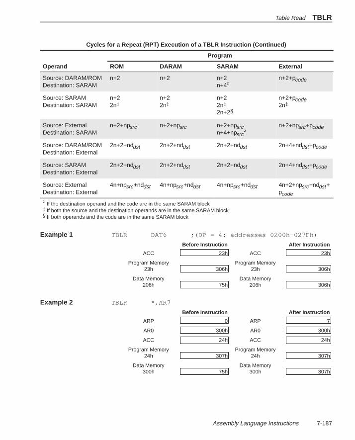
Table Read TBLR
7-187 Assembly Language Instructions
Cycles for a Repeat (RPT) Execution of a TBLR Instruction (Continued)
Program
Operand ROM DARAM SARAM External
Source: DARAM/ROMDestination: SARAM
n+2 n+2 n+2n+4†
n+2+pcode
Source: SARAMDestination: SARAM
n+22n‡
n+22n‡
n+22n‡
2n+2§
n+2+pcode2n‡
Source: ExternalDestination: SARAM
n+2+npsrc n+2+npsrc n+2+npsrcn+4+npsrc†
n+2+npsrc+pcode
Source: DARAM/ROMDestination: External
2n+2+nddst 2n+2+nddst 2n+2+nddst 2n+4+nddst+pcode
Source: SARAMDestination: External
2n+2+nddst 2n+2+nddst 2n+2+nddst 2n+4+nddst+pcode
Source: ExternalDestination: External
4n+npsrc+nddst 4n+npsrc+nddst 4n+npsrc+nddst 4n+2+npsrc+nddst+pcode
† If the destination operand and the code are in the same SARAM block‡ If both the source and the destination operands are in the same SARAM block§ If both operands and the code are in the same SARAM block
Example 1 TBLR DAT6 ;(DP = 4: addresses 0200h–027Fh)
Before Instruction After Instruction
ACC 23h ACC 23h
Program Memory Program Memory23h 306h 23h 306h
Data Memory Data Memory206h 75h 206h 306h
Example 2 TBLR *,AR7
Before Instruction After Instruction
ARP 0 ARP 7
AR0 300h AR0 300h
ACC 24h ACC 24h
Program Memory Program Memory24h 307h 24h 307h
Data Memory Data Memory300h 75h 300h 307h
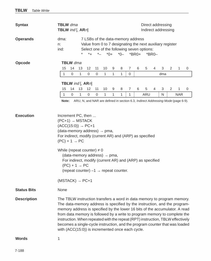
TBLW Table Write
7-188
Syntax TBLW dma Direct addressingTBLW ind [, ARn] Indirect addressing
Operands dma: 7 LSBs of the data-memory addressn: Value from 0 to 7 designating the next auxiliary registerind: Select one of the following seven options:
* *+ *– *0+ *0– *BR0+ *BR0–
TBLW dma15 14 13 12 11 10 9 8 7 6 5 4 3 2 1 0
1 0 1 0 0 1 1 1 0 dma
TBLW ind [, ARn]15 14 13 12 11 10 9 8 7 6 5 4 3 2 1 0
1 0 1 0 0 1 1 1 1 ARU N NAR
Note: ARU, N, and NAR are defined in section 6.3, Indirect Addressing Mode (page 6-9).
Execution Increment PC, then ...(PC+1) → MSTACK(ACC(15:0)) → PC+1(data-memory address) → pma,For indirect, modify (current AR) and (ARP) as specified(PC) + 1 → PC
While (repeat counter) ≠ 0(data-memory address) → pma,For indirect, modify (current AR) and (ARP) as specified(PC) + 1 → PC(repeat counter) –1 → repeat counter.
(MSTACK) → PC+1
Status Bits None
Description The TBLW instruction transfers a word in data memory to program memory.The data-memory address is specified by the instruction, and the program-memory address is specified by the lower 16 bits of the accumulator. A readfrom data memory is followed by a write to program memory to complete theinstruction. When repeated with the repeat (RPT) instruction, TBLW effectivelybecomes a single-cycle instruction, and the program counter that was loadedwith (ACC(15:0)) is incremented once each cycle.
Words 1
Opcode
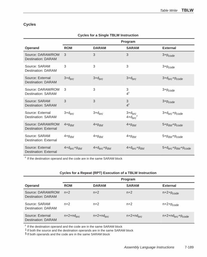
Table Write TBLW
7-189 Assembly Language Instructions
Cycles
Cycles for a Single TBLW Instruction
Program
Operand ROM DARAM SARAM External
Source: DARAM/ROMDestination: DARAM
3 3 3 3+pcode
Source: SARAMDestination: DARAM
3 3 3 3+pcode
Source: ExternalDestination: DARAM
3+dsrc 3+dsrc 3+dsrc 3+dsrc+pcode
Source: DARAM/ROMDestination: SARAM
3 3 34†
3+pcode
Source: SARAMDestination: SARAM
3 3 34†
3+pcode
Source: ExternalDestination: SARAM
3+dsrc 3+dsrc 3+dsrc4+dsrc†
3+dsrc+pcode
Source: DARAM/ROMDestination: External
4+pdst 4+pdst 4+pdst 5+pdst+pcode
Source: SARAMDestination: External
4+pdst 4+pdst 4+pdst 5+pdst+pcode
Source: ExternalDestination: External
4+dsrc+pdst 4+dsrc+pdst 4+dsrc+pdst 5+dsrc+pdst+pcode
† If the destination operand and the code are in the same SARAM block
Cycles for a Repeat (RPT) Execution of a TBLW Instruction
Program
Operand ROM DARAM SARAM External
Source: DARAM/ROMDestination: DARAM
n+2 n+2 n+2 n+2+pcode
Source: SARAMDestination: DARAM
n+2 n+2 n+2 n+2+pcode
Source: ExternalDestination: DARAM
n+2+ndsrc n+2+ndsrc n+2+ndsrc n+2+ndsrc+pcode
† If the destination operand and the code are in the same SARAM block‡ If both the source and the destination operands are in the same SARAM block§ If both operands and the code are in the same SARAM block
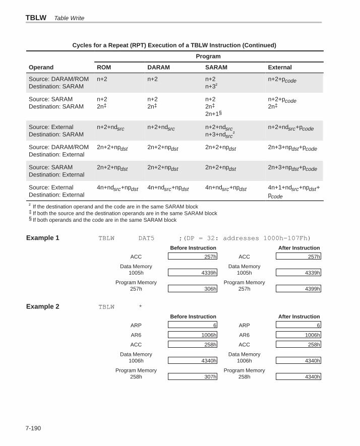
TBLW Table Write
7-190
Cycles for a Repeat (RPT) Execution of a TBLW Instruction (Continued)
Program
Operand ROM DARAM SARAM External
Source: DARAM/ROMDestination: SARAM
n+2 n+2 n+2n+3†
n+2+pcode
Source: SARAMDestination: SARAM
n+22n‡
n+22n‡
n+22n‡
2n+1§
n+2+pcode2n‡
Source: ExternalDestination: SARAM
n+2+ndsrc n+2+ndsrc n+2+ndsrcn+3+ndsrc†
n+2+ndsrc+pcode
Source: DARAM/ROMDestination: External
2n+2+npdst 2n+2+npdst 2n+2+npdst 2n+3+npdst+pcode
Source: SARAMDestination: External
2n+2+npdst 2n+2+npdst 2n+2+npdst 2n+3+npdst+pcode
Source: ExternalDestination: External
4n+ndsrc+npdst 4n+ndsrc+npdst 4n+ndsrc+npdst 4n+1+ndsrc+npdst+pcode
† If the destination operand and the code are in the same SARAM block‡ If both the source and the destination operands are in the same SARAM block§ If both operands and the code are in the same SARAM block
Example 1 TBLW DAT5 ;(DP = 32: addresses 1000h–107Fh)
Before Instruction After Instruction
ACC 257h ACC 257h
Data Memory Data Memory1005h 4339h 1005h 4339h
Program Memory Program Memory257h 306h 257h 4399h
Example 2 TBLW *
Before Instruction After Instruction
ARP 6 ARP 6
AR6 1006h AR6 1006h
ACC 258h ACC 258h
Data Memory Data Memory1006h 4340h 1006h 4340h
Program Memory Program Memory258h 307h 258h 4340h
Software Interrupt TRAP
7-191 Assembly Language Instructions
Syntax TRAP
Operands None
Opcode 01234567891011121314151000101001111101
Execution (PC) + 1 → stack22h → PC
Status Bits Not affected by INTM; does not affect INTM.
Description The TRAP instruction is a software interrupt that transfers program control toprogram-memory location 22h and pushes the program counter (PC) plus 1onto the hardware stack. The instruction at location 22h may contain a branchinstruction to transfer control to the TRAP routine. Putting (PC + 1) onto thestack enables a return instruction to pop the return address (which points tothe instruction after TRAP) from the stack. The TRAP instruction is not mask-able.
Words 1
Cycles for a Single TRAP Instruction
ROM DARAM SARAM External
4 4 4 4+3p†
† The processor performs speculative fetching by reading two additional instruction words. If thePC discontinuity is taken, these two instruction words are discarded.
Example TRAP ;PC + 1 is pushed onto the stack, and then;control is passed to program memory location;22h.
Cycles
XOR Exclusive OR With Accumulator
7-192
Syntax XOR dma Direct addressingXOR ind [, ARn] Indirect addressingXOR #lk [, shift ] Long immediate addressingXOR #lk,16 Long immediate with left
shift of 16
Operands dma: 7 LSBs of the data-memory addressshift: Left shift value from 0 to 15 (defaults to 0)n: Value from 0 to 7 designating the next auxiliary registerlk: 16-bit long immediate valueind: Select one of the following seven options:
* *+ *– *0+ *0– *BR0+ *BR0–
XOR dma15 14 13 12 11 10 9 8 7 6 5 4 3 2 1 0
0 1 1 0 1 1 0 0 0 dma
XOR ind [, ARn]15 14 13 12 11 10 9 8 7 6 5 4 3 2 1 0
0 1 1 0 1 1 0 0 1 ARU N NAR
Note: ARU, N, and NAR are defined in section 6.3, Indirect Addressing Mode (page 6-9).
XOR #lk [, shift]15 14 13 12 11 10 9 8 7 6 5 4 3 2 1 0
1 0 1 1 1 1 1 1 1 1 0 1 shift
lk
XOR #lk, 1615 14 13 12 11 10 9 8 7 6 5 4 3 2 1 0
1 0 1 1 1 1 1 0 1 0 0 0 0 0 1 1
lk
Execution Increment PC, then ...Event(s) Addressing mode(ACC(15:0)) XOR (data-memory address) → ACC(15:0) Direct or indirect(ACC(31:16)) → ACC(31:16)
(ACC(31:0)) XOR lk 2shift → ACC(31:0) Long immediate
(ACC(31:0)) XOR lk 216→ ACC(31:0) Long immediatewith left shift of 16
Opcode
Exclusive OR With Accumulator XOR
7-193 Assembly Language Instructions
Status Bits None
Description With direct or indirect addressing, the low half of the accumulator value isexclusive ORed with the content of the addressed data memory location, andthe result replaces the low half of the accumulator value; the upper half of theaccumulator value is unaffected. With immediate addressing, the long imme-diate constant is shifted and zero filled on both ends and exclusive ORed withthe entire content of the accumulator. The carry bit (C) is unaffected by XOR.
Words Words Addressing mode1 Direct or indirect
2 Long immediate
Cycles for a Single XOR Instruction (Using Direct and Indirect Addressing)
Program
Operand ROM DARAM SARAM External
DARAM 1 1 1 1+p
SARAM 1 1 1, 2† 1+p
External 1+d 1+d 1+d 2+d+p
† If the operand and the code are in the same SARAM block
Cycles for a Repeat (RPT) Execution of an XOR Instruction (Using Directand Indirect Addressing)
Program
Operand ROM DARAM SARAM External
DARAM n n n n+p
SARAM n n n, n+1† n+p
External n+nd n+nd n+nd n+1+p+nd
† If the operand and the code are in the same SARAM block
Cycles for a Single XOR Instruction (Using Long Immediate Addressing)
ROM DARAM SARAM External
2 2 2 2+2p
Cycles
XOR Exclusive OR With Accumulator
7-194
Example 1 XOR DAT127 ;(DP = 511: addresses FF80h–FFFFh)
Before Instruction After Instruction
Data Memory Data Memory0FFFFh 0F0F0h 0FFFFh 0F0F0h
ACC X 12345678h ACC X 1234A688h
C C
Example 2 XOR *+,AR0
Before Instruction After Instruction
ARP 7 ARP 0
AR7 300h AR7 301h
Data Memory Data Memory300h 0FFFFh 300h 0FFFFh
ACC X 1234F0F0h ACC X 12340F0Fh
C C
Example 3 XOR #0F0F0h,4 ;(First shift data value left by;four)
Before Instruction After Instruction
ACC X 11111010h ACC X 111E1F10h
C C
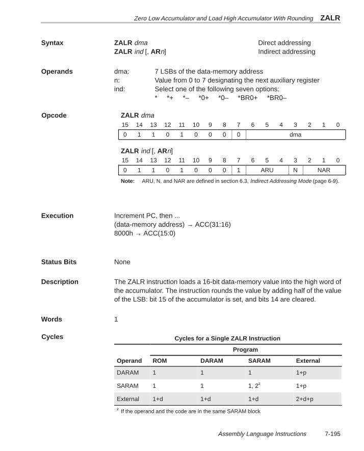
Zero Low Accumulator and Load High Accumulator With Rounding ZALR
7-195 Assembly Language Instructions
Syntax ZALR dma Direct addressingZALR ind [, ARn] Indirect addressing
Operands dma: 7 LSBs of the data-memory addressn: Value from 0 to 7 designating the next auxiliary registerind: Select one of the following seven options:
* *+ *– *0+ *0– *BR0+ *BR0–
ZALR dma15 14 13 12 11 10 9 8 7 6 5 4 3 2 1 0
0 1 1 0 1 0 0 0 0 dma
ZALR ind [, ARn]15 14 13 12 11 10 9 8 7 6 5 4 3 2 1 0
0 1 1 0 1 0 0 0 1 ARU N NAR
Note: ARU, N, and NAR are defined in section 6.3, Indirect Addressing Mode (page 6-9).
Execution Increment PC, then ...(data-memory address) → ACC(31:16)8000h → ACC(15:0)
Status Bits None
Description The ZALR instruction loads a 16-bit data-memory value into the high word ofthe accumulator. The instruction rounds the value by adding half of the valueof the LSB: bit 15 of the accumulator is set, and bits 14 are cleared.
Words 1
Cycles for a Single ZALR Instruction
Program
Operand ROM DARAM SARAM External
DARAM 1 1 1 1+p
SARAM 1 1 1, 2† 1+p
External 1+d 1+d 1+d 2+d+p
† If the operand and the code are in the same SARAM block
Opcode
Cycles
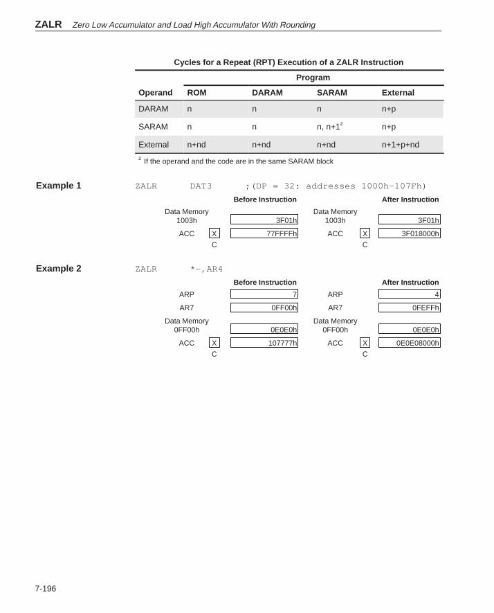
ZALR Zero Low Accumulator and Load High Accumulator With Rounding
7-196
Cycles for a Repeat (RPT) Execution of a ZALR Instruction
Program
Operand ROM DARAM SARAM External
DARAM n n n n+p
SARAM n n n, n+1† n+p
External n+nd n+nd n+nd n+1+p+nd
† If the operand and the code are in the same SARAM block
Example 1 ZALR DAT3 ;(DP = 32: addresses 1000h–107Fh)
Before Instruction After Instruction
Data Memory Data Memory1003h 3F01h 1003h 3F01h
ACC X 77FFFFh ACC X 3F018000h
C C
Example 2 ZALR *–,AR4
Before Instruction After Instruction
ARP 7 ARP 4
AR7 0FF00h AR7 0FEFFh
Data Memory Data Memory0FF00h 0E0E0h 0FF00h 0E0E0h
ACC X 107777h ACC X 0E0E08000h
C C
A-1
Appendix A
TMS320C1x/C2x/C20x/C5xInstruction Set Comparison
This appendix contains a table that compares the TMS320C1x, TMS320C2x,TMS320C20x, and TMS320C5x instructions alphabetically. Each table entryshows the syntax for the instruction, indicates which devices support theinstruction, and describes the operation of the instruction. Section A.1 showsa sample table entry and describes the symbols and abbreviations used in thetable.
The TMS320C2x, TMS320C20x, and TMS320C5x devices have enhancedinstructions; enhanced instructions are single mnemonics that perform thefunctions of several similar instructions. Section A.2 summarizes theenhanced instructions.
This appendix does not cover topics such as opcodes, instruction timing, oraddressing modes; in addition to this book, the following documents coversuch topics in detail:
TMS320C1x User’s Guide (literature number SPRU013)
TMS320C2x User’s Guide (literature number SPRU014)
TMS320C5x User’s Guide (literature number SPRU056)
Topic Page
A.1 Using the Instruction Set Comparison Table A-2. . . . . . . . . . . . . . . . . . . . .
A.2 Enhanced Instructions A-5. . . . . . . . . . . . . . . . . . . . . . . . . . . . . . . . . . . . . . . .
A.3 Instruction Set Comparison Table A-6. . . . . . . . . . . . . . . . . . . . . . . . . . . . . .
Appendix A
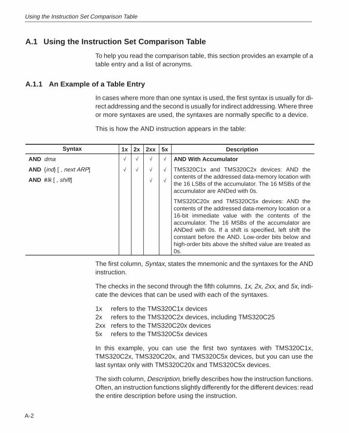
Using the Instruction Set Comparison Table
A-2
A.1 Using the Instruction Set Comparison Table
To help you read the comparison table, this section provides an example of atable entry and a list of acronyms.
A.1.1 An Example of a Table Entry
In cases where more than one syntax is used, the first syntax is usually for di-rect addressing and the second is usually for indirect addressing. Where threeor more syntaxes are used, the syntaxes are normally specific to a device.
This is how the AND instruction appears in the table:
Syntax 1x 2x 2xx 5x Description
AND dma
AND ind [ , next ARP]
AND #lk [ , shift]
√
√
√
√
√
√
√
√
√
√
AND With Accumulator
TMS320C1x and TMS320C2x devices: AND thecontents of the addressed data-memory location withthe 16 LSBs of the accumulator. The 16 MSBs of theaccumulator are ANDed with 0s.
TMS320C20x and TMS320C5x devices: AND thecontents of the addressed data-memory location or a16-bit immediate value with the contents of theaccumulator. The 16 MSBs of the accumulator areANDed with 0s. If a shift is specified, left shift theconstant before the AND. Low-order bits below andhigh-order bits above the shifted value are treated as0s.
The first column, Syntax, states the mnemonic and the syntaxes for the ANDinstruction.
The checks in the second through the fifth columns, 1x, 2x, 2xx, and 5x, indi-cate the devices that can be used with each of the syntaxes.
1x refers to the TMS320C1x devices2x refers to the TMS320C2x devices, including TMS320C252xx refers to the TMS320C20x devices5x refers to the TMS320C5x devices
In this example, you can use the first two syntaxes with TMS320C1x,TMS320C2x, TMS320C20x, and TMS320C5x devices, but you can use thelast syntax only with TMS320C20x and TMS320C5x devices.
The sixth column, Description, briefly describes how the instruction functions.Often, an instruction functions slightly differently for the different devices: readthe entire description before using the instruction.
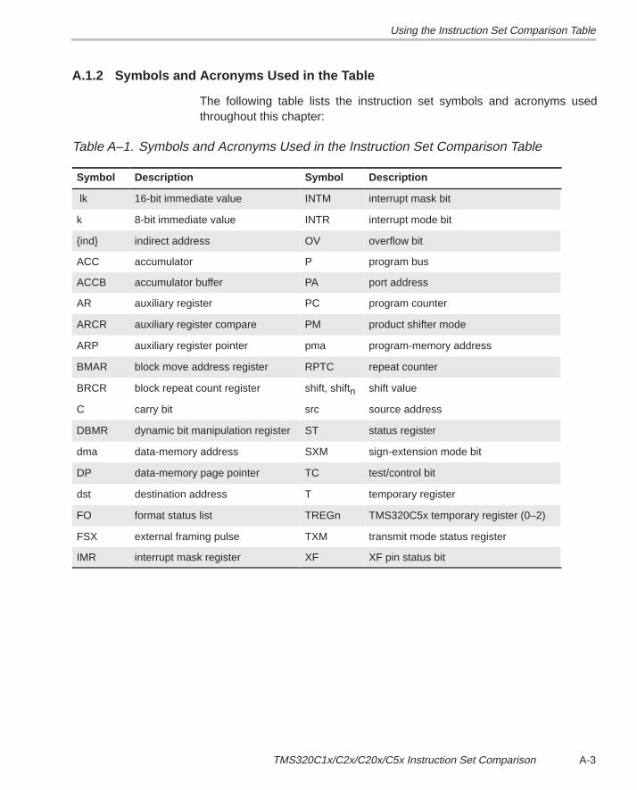
Using the Instruction Set Comparison Table
A-3TMS320C1x/C2x/C20x/C5x Instruction Set Comparison
A.1.2 Symbols and Acronyms Used in the Table
The following table lists the instruction set symbols and acronyms usedthroughout this chapter:
Table A–1. Symbols and Acronyms Used in the Instruction Set Comparison Table
Symbol Description Symbol Description
lk 16-bit immediate value INTM interrupt mask bit
k 8-bit immediate value INTR interrupt mode bit
ind indirect address OV overflow bit
ACC accumulator P program bus
ACCB accumulator buffer PA port address
AR auxiliary register PC program counter
ARCR auxiliary register compare PM product shifter mode
ARP auxiliary register pointer pma program-memory address
BMAR block move address register RPTC repeat counter
BRCR block repeat count register shift, shiftn shift value
C carry bit src source address
DBMR dynamic bit manipulation register ST status register
dma data-memory address SXM sign-extension mode bit
DP data-memory page pointer TC test/control bit
dst destination address T temporary register
FO format status list TREGn TMS320C5x temporary register (0–2)
FSX external framing pulse TXM transmit mode status register
IMR interrupt mask register XF XF pin status bit
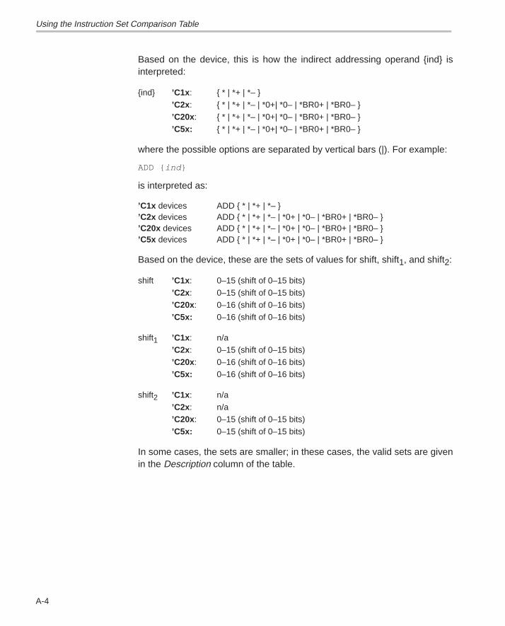
Using the Instruction Set Comparison Table
A-4
Based on the device, this is how the indirect addressing operand ind isinterpreted:
ind ’C1x : * | *+ | *– ’C2x : * | *+ | *– | *0+| *0– | *BR0+ | *BR0– ’C20x : * | *+ | *– | *0+| *0– | *BR0+ | *BR0– ’C5x: * | *+ | *– | *0+| *0– | *BR0+ | *BR0–
where the possible options are separated by vertical bars (|). For example:
ADD ind
is interpreted as:
’C1x devices ADD * | *+ | *– ’C2x devices ADD * | *+ | *– | *0+ | *0– | *BR0+ | *BR0– ’C20x devices ADD * | *+ | *– | *0+ | *0– | *BR0+ | *BR0– ’C5x devices ADD * | *+ | *– | *0+ | *0– | *BR0+ | *BR0–
Based on the device, these are the sets of values for shift, shift1, and shift2:
shift ’C1x : 0–15 (shift of 0–15 bits)’C2x : 0–15 (shift of 0–15 bits)’C20x : 0–16 (shift of 0–16 bits)’C5x: 0–16 (shift of 0–16 bits)
shift1 ’C1x : n/a’C2x : 0–15 (shift of 0–15 bits)’C20x : 0–16 (shift of 0–16 bits)’C5x: 0–16 (shift of 0–16 bits)
shift2 ’C1x : n/a’C2x : n/a’C20x : 0–15 (shift of 0–15 bits)’C5x: 0–15 (shift of 0–15 bits)
In some cases, the sets are smaller; in these cases, the valid sets are givenin the Description column of the table.
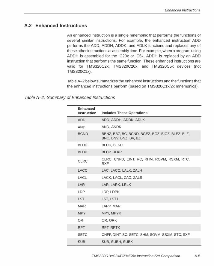
Enhanced Instructions
A-5TMS320C1x/C2x/C20x/C5x Instruction Set Comparison
A.2 Enhanced Instructions
An enhanced instruction is a single mnemonic that performs the functions ofseveral similar instructions. For example, the enhanced instruction ADDperforms the ADD, ADDH, ADDK, and ADLK functions and replaces any ofthese other instructions at assembly time. For example, when a program usingADDH is assembled for the ’C20x or ’C5x, ADDH is replaced by an ADDinstruction that performs the same function. These enhanced instructions arevalid for TMS320C2x, TMS320C20x, and TMS320C5x devices (notTMS320C1x).
Table A–2 below summarizes the enhanced instructions and the functions thatthe enhanced instructions perform (based on TMS320C1x/2x mnemonics).
Table A–2. Summary of Enhanced Instructions
EnhancedInstruction Includes These Operations
ADD ADD, ADDH, ADDK, ADLK
AND AND, ANDK
BCND BBNZ, BBZ, BC, BCND, BGEZ, BGZ, BIOZ, BLEZ, BLZ,BNC, BNV, BNZ, BV, BZ
BLDD BLDD, BLKD
BLDP BLDP, BLKP
CLRC CLRC, CNFD, EINT, RC, RHM, ROVM, RSXM, RTC,RXF
LACC LAC, LACC, LALK, ZALH
LACL LACK, LACL, ZAC, ZALS
LAR LAR, LARK, LRLK
LDP LDP, LDPK
LST LST, LST1
MAR LARP, MAR
MPY MPY, MPYK
OR OR, ORK
RPT RPT, RPTK
SETC CNFP, DINT, SC, SETC, SHM, SOVM, SSXM, STC, SXF
SUB SUB, SUBH, SUBK
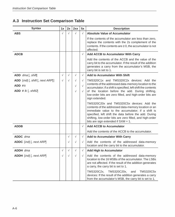
Instruction Set Comparison Table
A-6
A.3 Instruction Set Comparison Table
Syntax 1x 2x 2xx 5x Description
ABS √ √ √ √ Absolute Value of Accumulator
If the contents of the accumulator are less than zero,replace the contents with the 2s complement of thecontents. If the contents are ≥ 0, the accumulator is notaffected.
ADCB √ Add ACCB to Accumulator With Carry
Add the contents of the ACCB and the value of thecarry bit to the accumulator. If the result of the additiongenerates a carry from the accumulator’s MSB, thecarry bit is set to 1.
ADD dma [, shift]
ADD ind [, shift [, next ARP] ]
ADD # k
ADD # lk [, shift2]
√
√
√
√
√
√
√
√
√
√
√
√
Add to Accumulator With Shift
TMS320C1x and TMS320C2x devices: Add thecontents of the addressed data-memory location to theaccumulator; if a shift is specified, left shift the contentsof the location before the add. During shifting,low-order bits are zero filled, and high-order bits aresign extended.
TMS320C20x and TMS320C5x devices: Add thecontents of the addressed data-memory location or animmediate value to the accumulator; if a shift isspecified, left shift the data before the add. Duringshifting, low-order bits are zero filled, and high-orderbits are sign extended if SXM = 1.
ADDB √ Add ACCB to Accumulator
Add the contents of the ACCB to the accumulator.
ADDC dma
ADDC ind [, next ARP]
√
√
√
√
√
√
Add to Accumulator With Carry
Add the contents of the addressed data-memorylocation and the carry bit to the accumulator.
ADDH dma
ADDH ind [, next ARP]
√
√
√
√
√
√
√
√
Add High to Accumulator
Add the contents of the addressed data-memorylocation to the 16 MSBs of the accumulator. The LSBsare not affected. If the result of the addition generatesa carry, the carry bit is set to 1.
TMS320C2x, TMS320C20x, and TMS320C5xdevices: If the result of the addition generates a carryfrom the accumulator’s MSB, the carry bit is set to 1.
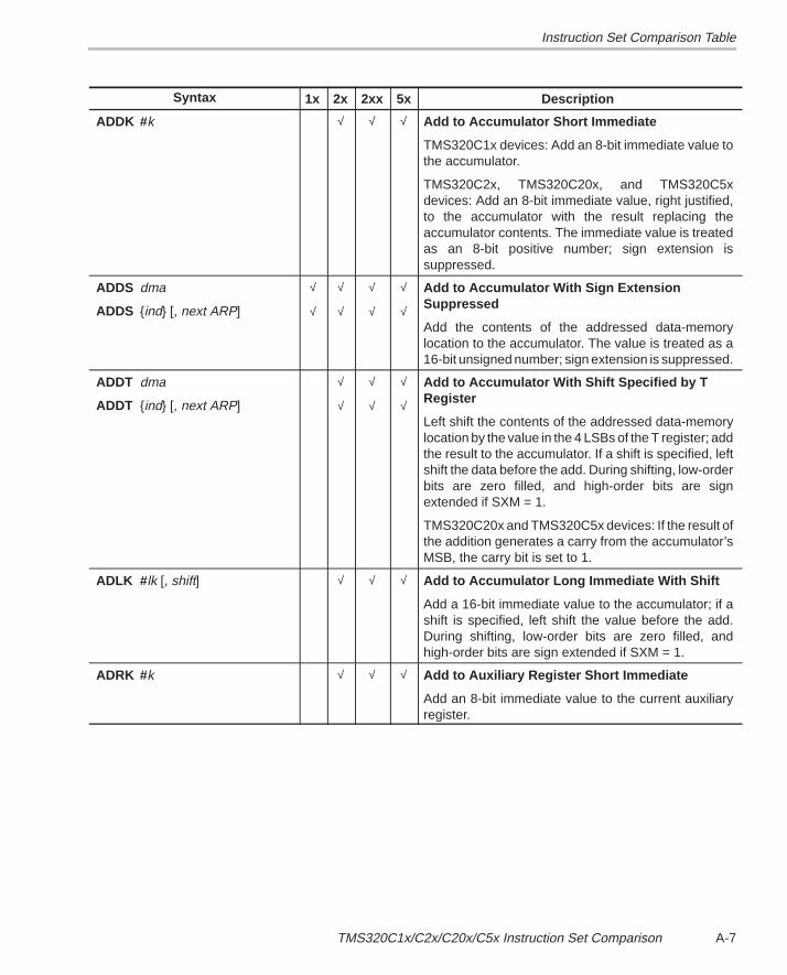
Instruction Set Comparison Table
A-7TMS320C1x/C2x/C20x/C5x Instruction Set Comparison
Syntax Description5x2xx2x1x
ADDK #k √ √ √ Add to Accumulator Short Immediate
TMS320C1x devices: Add an 8-bit immediate value tothe accumulator.
TMS320C2x, TMS320C20x, and TMS320C5xdevices: Add an 8-bit immediate value, right justified,to the accumulator with the result replacing theaccumulator contents. The immediate value is treatedas an 8-bit positive number; sign extension issuppressed.
ADDS dma
ADDS ind [, next ARP]
√
√
√
√
√
√
√
√
Add to Accumulator With Sign Extension Suppressed
Add the contents of the addressed data-memorylocation to the accumulator. The value is treated as a16-bit unsigned number; sign extension is suppressed.
ADDT dma
ADDT ind [, next ARP]
√
√
√
√
√
√
Add to Accumulator With Shift Specified by TRegister
Left shift the contents of the addressed data-memorylocation by the value in the 4 LSBs of the T register; addthe result to the accumulator. If a shift is specified, leftshift the data before the add. During shifting, low-orderbits are zero filled, and high-order bits are signextended if SXM = 1.
TMS320C20x and TMS320C5x devices: If the result ofthe addition generates a carry from the accumulator’sMSB, the carry bit is set to 1.
ADLK # lk [, shift] √ √ √ Add to Accumulator Long Immediate With Shift
Add a 16-bit immediate value to the accumulator; if ashift is specified, left shift the value before the add.During shifting, low-order bits are zero filled, andhigh-order bits are sign extended if SXM = 1.
ADRK #k √ √ √ Add to Auxiliary Register Short Immediate
Add an 8-bit immediate value to the current auxiliaryregister.
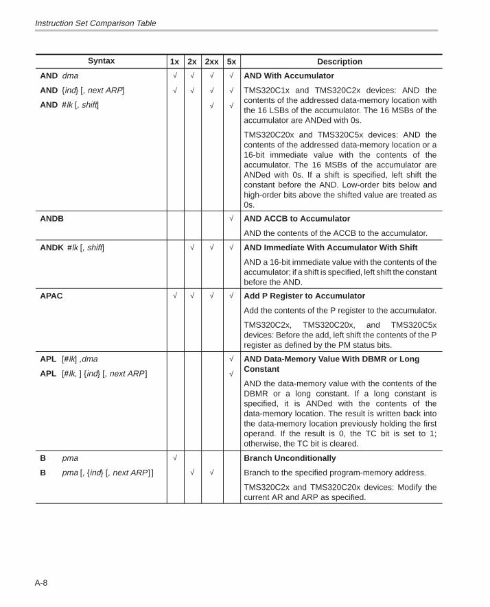
Instruction Set Comparison Table
A-8
Syntax Description5x2xx2x1x
AND dma
AND ind [, next ARP]
AND #lk [, shift]
√
√
√
√
√
√
√
√
√
√
AND With Accumulator
TMS320C1x and TMS320C2x devices: AND thecontents of the addressed data-memory location withthe 16 LSBs of the accumulator. The 16 MSBs of theaccumulator are ANDed with 0s.
TMS320C20x and TMS320C5x devices: AND thecontents of the addressed data-memory location or a16-bit immediate value with the contents of theaccumulator. The 16 MSBs of the accumulator areANDed with 0s. If a shift is specified, left shift theconstant before the AND. Low-order bits below andhigh-order bits above the shifted value are treated as0s.
ANDB √ AND ACCB to Accumulator
AND the contents of the ACCB to the accumulator.
ANDK # lk [, shift] √ √ √ AND Immediate With Accumulator With Shift
AND a 16-bit immediate value with the contents of theaccumulator; if a shift is specified, left shift the constantbefore the AND.
APAC √ √ √ √ Add P Register to Accumulator
Add the contents of the P register to the accumulator.
TMS320C2x, TMS320C20x, and TMS320C5xdevices: Before the add, left shift the contents of the Pregister as defined by the PM status bits.
APL [#lk] ,dma
APL [#lk, ] ind [, next ARP]
√
√
AND Data-Memory Value With DBMR or LongConstant
AND the data-memory value with the contents of theDBMR or a long constant. If a long constant isspecified, it is ANDed with the contents of thedata-memory location. The result is written back intothe data-memory location previously holding the firstoperand. If the result is 0, the TC bit is set to 1;otherwise, the TC bit is cleared.
B pma
B pma [, ind [, next ARP] ]
√
√ √
Branch Unconditionally
Branch to the specified program-memory address.
TMS320C2x and TMS320C20x devices: Modify thecurrent AR and ARP as specified.
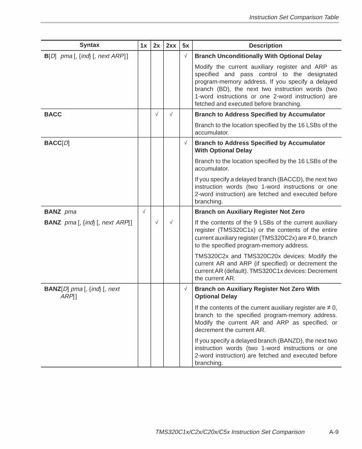
Instruction Set Comparison Table
A-9TMS320C1x/C2x/C20x/C5x Instruction Set Comparison
Syntax Description5x2xx2x1x
B[D] pma [, ind [, next ARP] ] √ Branch Unconditionally With Optional Delay
Modify the current auxiliary register and ARP asspecified and pass control to the designatedprogram-memory address. If you specify a delayedbranch (BD), the next two instruction words (two1-word instructions or one 2-word instruction) arefetched and executed before branching.
BACC √ √ Branch to Address Specified by Accumulator
Branch to the location specified by the 16 LSBs of theaccumulator.
BACC [D] √ Branch to Address Specified by AccumulatorWith Optional Delay
Branch to the location specified by the 16 LSBs of theaccumulator.
If you specify a delayed branch (BACCD), the next twoinstruction words (two 1-word instructions or one2-word instruction) are fetched and executed beforebranching.
BANZ pma
BANZ pma [, ind [, next ARP] ]
√
√ √
Branch on Auxiliary Register Not Zero
If the contents of the 9 LSBs of the current auxiliaryregister (TMS320C1x) or the contents of the entirecurrent auxiliary register (TMS320C2x) are ≠ 0, branchto the specified program-memory address.
TMS320C2x and TMS320C20x devices: Modify thecurrent AR and ARP (if specified) or decrement thecurrent AR (default). TMS320C1x devices: Decrementthe current AR.
BANZ [D] pma [, ind [, nextARP] ]
√ Branch on Auxiliary Register Not Zero With Optional Delay
If the contents of the current auxiliary register are ≠ 0,branch to the specified program-memory address.Modify the current AR and ARP as specified, ordecrement the current AR.
If you specify a delayed branch (BANZD), the next twoinstruction words (two 1-word instructions or one2-word instruction) are fetched and executed beforebranching.
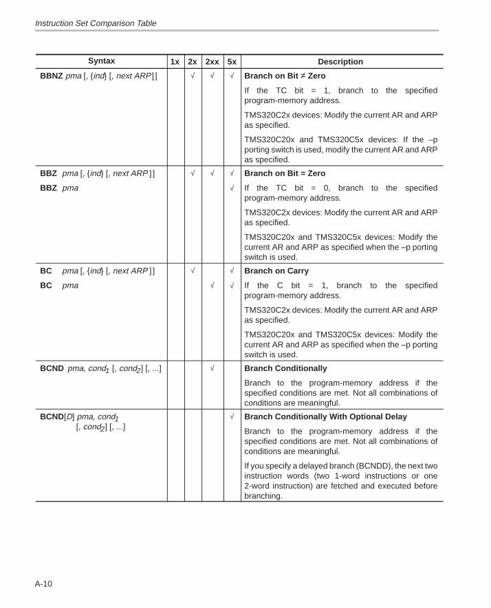
Instruction Set Comparison Table
A-10
Syntax Description5x2xx2x1x
BBNZ pma [, ind [, next ARP] ] √ √ √ Branch on Bit ≠ Zero
If the TC bit = 1, branch to the specifiedprogram-memory address.
TMS320C2x devices: Modify the current AR and ARPas specified.
TMS320C20x and TMS320C5x devices: If the –pporting switch is used, modify the current AR and ARPas specified.
BBZ pma [, ind [, next ARP ] ]
BBZ pma
√ √ √
√
Branch on Bit = Zero
If the TC bit = 0, branch to the specifiedprogram-memory address.
TMS320C2x devices: Modify the current AR and ARPas specified.
TMS320C20x and TMS320C5x devices: Modify thecurrent AR and ARP as specified when the –p portingswitch is used.
BC pma [, ind [, next ARP ] ]
BC pma
√
√
√
√
Branch on Carry
If the C bit = 1, branch to the specifiedprogram-memory address.
TMS320C2x devices: Modify the current AR and ARPas specified.
TMS320C20x and TMS320C5x devices: Modify thecurrent AR and ARP as specified when the –p portingswitch is used.
BCND pma, cond1 [, cond2] [, ...] √ Branch Conditionally
Branch to the program-memory address if thespecified conditions are met. Not all combinations ofconditions are meaningful.
BCND[D] pma, cond1[, cond2] [, ...]
√ Branch Conditionally With Optional Delay
Branch to the program-memory address if thespecified conditions are met. Not all combinations ofconditions are meaningful.
If you specify a delayed branch (BCNDD), the next twoinstruction words (two 1-word instructions or one2-word instruction) are fetched and executed beforebranching.
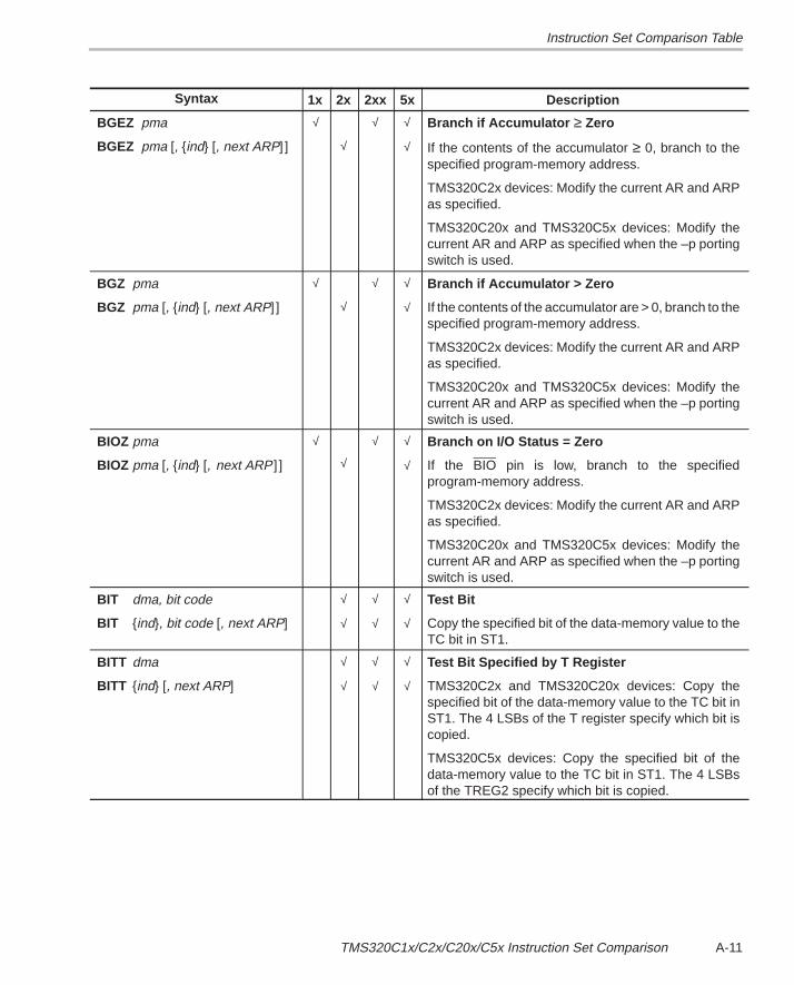
Instruction Set Comparison Table
A-11TMS320C1x/C2x/C20x/C5x Instruction Set Comparison
Syntax Description5x2xx2x1x
BGEZ pma
BGEZ pma [, ind [, next ARP] ]
√
√
√ √
√
Branch if Accumulator ≥ Zero
If the contents of the accumulator ≥ 0, branch to thespecified program-memory address.
TMS320C2x devices: Modify the current AR and ARPas specified.
TMS320C20x and TMS320C5x devices: Modify thecurrent AR and ARP as specified when the –p portingswitch is used.
BGZ pma
BGZ pma [, ind [, next ARP] ]
√
√
√ √
√
Branch if Accumulator > Zero
If the contents of the accumulator are > 0, branch to thespecified program-memory address.
TMS320C2x devices: Modify the current AR and ARPas specified.
TMS320C20x and TMS320C5x devices: Modify thecurrent AR and ARP as specified when the –p portingswitch is used.
BIOZ pma
BIOZ pma [, ind [, next ARP] ]
√
√
√ √
√
Branch on I/O Status = Zero
If the BIO pin is low, branch to the specifiedprogram-memory address.
TMS320C2x devices: Modify the current AR and ARPas specified.
TMS320C20x and TMS320C5x devices: Modify thecurrent AR and ARP as specified when the –p portingswitch is used.
BIT dma, bit code
BIT ind, bit code [, next ARP]
√
√
√
√
√
√
Test Bit
Copy the specified bit of the data-memory value to theTC bit in ST1.
BITT dma
BITT ind [, next ARP]
√
√
√
√
√
√
Test Bit Specified by T Register
TMS320C2x and TMS320C20x devices: Copy thespecified bit of the data-memory value to the TC bit inST1. The 4 LSBs of the T register specify which bit iscopied.
TMS320C5x devices: Copy the specified bit of thedata-memory value to the TC bit in ST1. The 4 LSBsof the TREG2 specify which bit is copied.
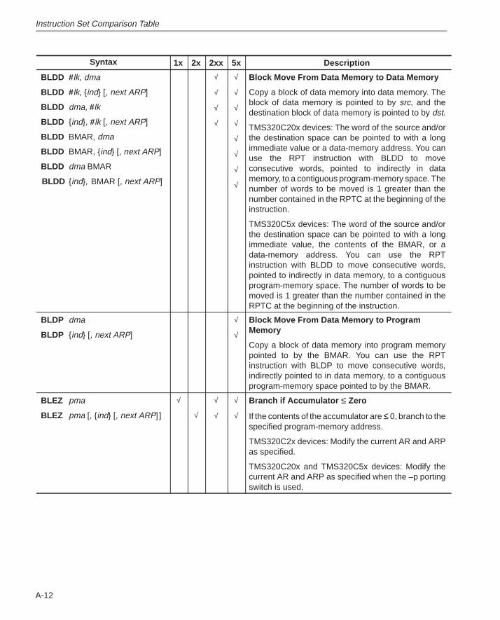
Instruction Set Comparison Table
A-12
Syntax Description5x2xx2x1x
BLDD # lk, dma
BLDD # lk, ind [, next ARP]
BLDD dma, #lk
BLDD ind, #lk [, next ARP]
BLDD BMAR, dma
BLDD BMAR, ind [, next ARP]
BLDD dma BMAR
BLDD ind, BMAR [, next ARP]
√
√
√
√
√
√
√
√
√
√
√
√
Block Move From Data Memory to Data Memory
Copy a block of data memory into data memory. Theblock of data memory is pointed to by src, and thedestination block of data memory is pointed to by dst.
TMS320C20x devices: The word of the source and/orthe destination space can be pointed to with a longimmediate value or a data-memory address. You canuse the RPT instruction with BLDD to moveconsecutive words, pointed to indirectly in datamemory, to a contiguous program-memory space. Thenumber of words to be moved is 1 greater than thenumber contained in the RPTC at the beginning of theinstruction.
TMS320C5x devices: The word of the source and/orthe destination space can be pointed to with a longimmediate value, the contents of the BMAR, or adata-memory address. You can use the RPTinstruction with BLDD to move consecutive words,pointed to indirectly in data memory, to a contiguousprogram-memory space. The number of words to bemoved is 1 greater than the number contained in theRPTC at the beginning of the instruction.
BLDP dma
BLDP ind [, next ARP]
√
√
Block Move From Data Memory to Program Memory
Copy a block of data memory into program memorypointed to by the BMAR. You can use the RPTinstruction with BLDP to move consecutive words,indirectly pointed to in data memory, to a contiguousprogram-memory space pointed to by the BMAR.
BLEZ pma
BLEZ pma [, ind [, next ARP] ]
√
√
√
√
√
√
Branch if Accumulator ≤ Zero
If the contents of the accumulator are ≤ 0, branch to thespecified program-memory address.
TMS320C2x devices: Modify the current AR and ARPas specified.
TMS320C20x and TMS320C5x devices: Modify thecurrent AR and ARP as specified when the –p portingswitch is used.
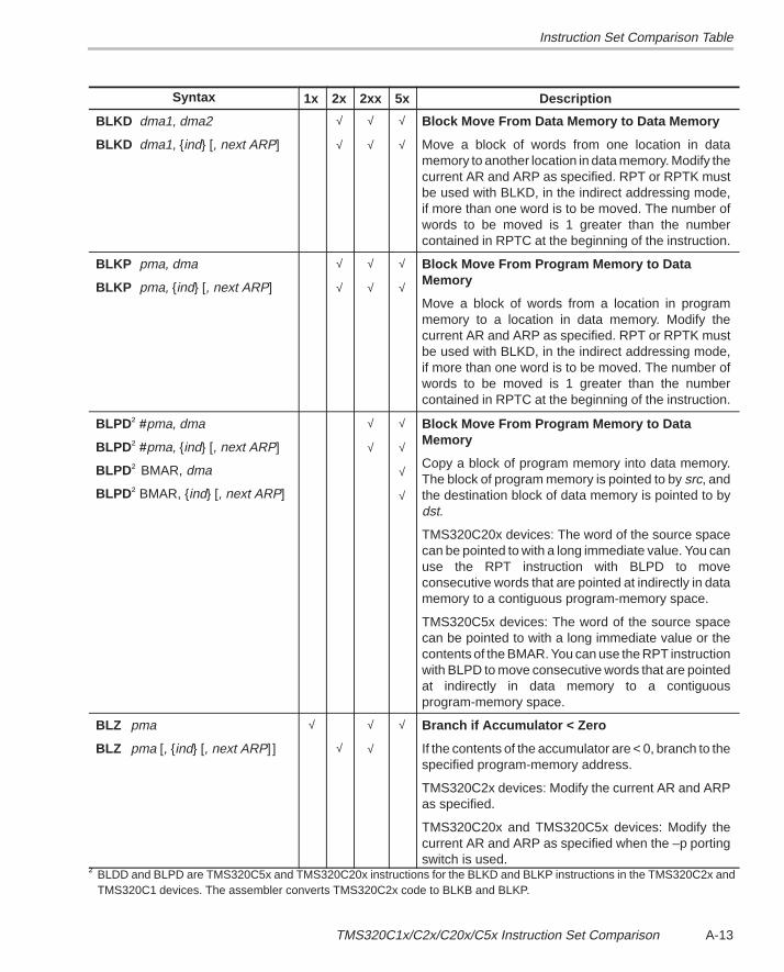
Instruction Set Comparison Table
A-13TMS320C1x/C2x/C20x/C5x Instruction Set Comparison
Syntax Description5x2xx2x1x
BLKD dma1, dma2
BLKD dma1, ind [, next ARP]
√
√
√
√
√
√
Block Move From Data Memory to Data Memory
Move a block of words from one location in datamemory to another location in data memory. Modify thecurrent AR and ARP as specified. RPT or RPTK mustbe used with BLKD, in the indirect addressing mode,if more than one word is to be moved. The number ofwords to be moved is 1 greater than the numbercontained in RPTC at the beginning of the instruction.
BLKP pma, dma
BLKP pma, ind [, next ARP]
√
√
√
√
√
√
Block Move From Program Memory to DataMemory
Move a block of words from a location in programmemory to a location in data memory. Modify thecurrent AR and ARP as specified. RPT or RPTK mustbe used with BLKD, in the indirect addressing mode,if more than one word is to be moved. The number ofwords to be moved is 1 greater than the numbercontained in RPTC at the beginning of the instruction.
BLPD†#pma, dma
BLPD†#pma, ind [, next ARP]
BLPD† BMAR, dma
BLPD†BMAR, ind [, next ARP]
√
√
√
√
√
√
Block Move From Program Memory to Data Memory
Copy a block of program memory into data memory.The block of program memory is pointed to by src, andthe destination block of data memory is pointed to bydst.
TMS320C20x devices: The word of the source spacecan be pointed to with a long immediate value. You canuse the RPT instruction with BLPD to moveconsecutive words that are pointed at indirectly in datamemory to a contiguous program-memory space.
TMS320C5x devices: The word of the source spacecan be pointed to with a long immediate value or thecontents of the BMAR. You can use the RPT instructionwith BLPD to move consecutive words that are pointedat indirectly in data memory to a contiguousprogram-memory space.
BLZ pma
BLZ pma [, ind [, next ARP] ]
√
√
√
√
√ Branch if Accumulator < Zero
If the contents of the accumulator are < 0, branch to thespecified program-memory address.
TMS320C2x devices: Modify the current AR and ARPas specified.
TMS320C20x and TMS320C5x devices: Modify thecurrent AR and ARP as specified when the –p portingswitch is used.
† BLDD and BLPD are TMS320C5x and TMS320C20x instructions for the BLKD and BLKP instructions in the TMS320C2x andTMS320C1 devices. The assembler converts TMS320C2x code to BLKB and BLKP.
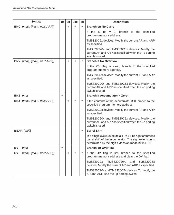
Instruction Set Comparison Table
A-14
Syntax 1x 2x 2xx 5x Description
BNC pma [, ind [, next ARP] ] √ √ √ Branch on No Carry
If the C bit = 0, branch to the specifiedprogram-memory address.
TMS320C2x devices: Modify the current AR and ARPas specified.
TMS320C20x and TMS320C5x devices: Modify thecurrent AR and ARP as specified when the –p portingswitch is used.
BNV pma [, ind [, next ARP] ] √ √ √ Branch if No Overflow
If the OV flag is clear, branch to the specifiedprogram-memory address.
TMS320C2x devices: Modify the current AR and ARPas specified.
TMS320C20x and TMS320C5x devices: Modify thecurrent AR and ARP as specified when the –p portingswitch is used.
BNZ pma
BNZ pma [, ind [, next ARP] ]
√
√ √ √
Branch if Accumulator ≠ Zero
If the contents of the accumulator ≠ 0, branch to thespecified program-memory address.
TMS320C2x devices: Modify the current AR and ARPas specified.
TMS320C20x and TMS320C5x devices: Modify thecurrent AR and ARP as specified when the –p portingswitch is used.
BSAR [shift] √ Barrel Shift
In a single cycle, execute a 1- to 16-bit right arithmeticbarrel shift of the accumulator. The sign extension isdetermined by the sign-extension mode bit in ST1.
BV pma
BV pma [, ind [, next ARP] ]
√
√ √ √
Branch on Overflow
If the OV flag is set, branch to the specifiedprogram-memory address and clear the OV flag.
TMS320C2x, TMS320C20x, and TMS320C5xdevices: Modify the current AR and ARP as specified.
TMS320C20x and TMS320C5x devices: To modify theAR and ARP, use the –p porting switch.
Instruction Set Comparison Table
A-15TMS320C1x/C2x/C20x/C5x Instruction Set Comparison
Syntax Description5x2xx2x1x
BZ pma
BZ pma [, ind [, next ARP]]
√
√
√ √ Branch if Accumulator = Zero
If the contents of the accumulator = 0, branch to thespecified program-memory address.
TMS320C2x, TMS320C20x and TMS320C5xdevices: Modify the current AR and ARP as specified.
TMS320C20x and TMS320C5x devices: To modify theAR and ARP, use the –p porting switch.
CALA √ √ √ Call Subroutine Indirect
The contents of the accumulator specify the addressof a subroutine. Increment the PC, push the PC ontothe stack, then load the 12 (TMS320C1x) or 16(TMS320C2x/C20x) LSBs of the accumulator into thePC.
CALA [D] √ Call Subroutine Indirect With Optional Delay
The contents of the accumulator specify the addressof a subroutine. Increment the PC and push it onto thestack; then load the 16 LSBs of the accumulator intothe PC.
If you specify a delayed branch (CALAD), the next twoinstruction words (two 1-word instructions or one2-word instruction) are fetched and executed beforethe call.
CALL pma
CALL pma [,ind [, next ARP] ]
√
√ √
Call Subroutine
The contents of the addressed program-memorylocation specify the address of a subroutine. Incrementthe PC by 2, push the PC onto the stack, then load thespecified program-memory address into the PC.
TMS320C2x and TMS320C20x devices: Modify thecurrent AR and ARP as specified.
CALL [D] pma [, ind [, nextARP] ]
√ Call Unconditionally With Optional Delay
The contents of the addressed program-memorylocation specify the address of a subroutine. Incrementthe PC and push the PC onto the stack; then load thespecified program-memory address (symbolic ornumeric) into the PC. Modify the current AR and ARPas specified.
If you specify a delayed branch (CALLD), the next twoinstruction words (two 1-word instructions or one2-word instruction) are fetched and executed beforethe call.
Instruction Set Comparison Table
A-16
Syntax Description5x2xx2x1x
CC pma, cond1 [, cond2] [, ...] √ Call Conditionally
If the specified conditions are met, control is passed tothe pma. Not all combinations of conditions aremeaningful.
CC[D] pma, cond1 [, cond2] [, ...] √ Call Conditionally With Optional Delay
If the specified conditions are met, control is passed tothe pma. Not all combinations of conditions aremeaningful.
If you specify a delayed branch (CCD), the next twoinstruction words (two 1-word instructions or one2-word instruction) are fetched and executed beforethe call.
CLRC control bit √ √ Clear Control Bit
Set the specified control bit to a logic 0. Maskableinterrupts are enabled immediately after the CLRCinstruction executes.
CMPL √ √ √ Complement Accumulator
Complement the contents of the accumulator (1scomplement).
CMPR CM √ √ √ Compare Auxiliary Register With AR0
Compare the contents of the current auxiliary registerto AR0, based on the following cases:
If CM = 002, test whether AR(ARP) = AR0.
If CM = 012, test whether AR(ARP) < AR0.
If CM = 102, test whether AR(ARP) > AR0.
If CM = 112, test whether AR(ARP) ≠ AR0.
If the result is true, load a 1 into the TC status bit;otherwise, load a 0 into the TC bit. The comparisondoes not affect the tested registers.
TMS320C5x devices: Compare the contents of theauxiliary register with the ARCR.
CNFD √ √ √ Configure Block as Data Memory
Configure on-chip RAM block B0 as data memory.Block B0 is mapped into data-memory locations512h–767h.
TMS320C5x devices: Block B0 is mapped intodata-memory locations 512h–1023h.
Instruction Set Comparison Table
A-17TMS320C1x/C2x/C20x/C5x Instruction Set Comparison
Syntax Description5x2xx2x1x
CNFP √ √ √ Configure Block as Program Memory
Configure on-chip RAM block B0 as program memory.Block B0 is mapped into program-memory locations65280h–65535h.
TMS320C5x devices: Block B0 is mapped intodata-memory locations 65024h–65535h.
CONF 2-bit constant √ Configure Block as Program Memory
Configure on-chip RAM block B0/B1/B2/B3 asprogram memory. For information on the memorymapping of B0/B1/B2/B3, see the TMS320C2x User’sGuide.
CPL [ #lk,] dma
CPL [ #lk,] ind [, next ARP]
√
√
Compare DBMR or Immediate With Data Value
Compare two quantities: If the two quantities areequal, set the TC bit to 1; otherwise, clear the TC bit.
CRGT √ Test for ACC > ACCB
Compare the contents of the ACC with the contents ofthe ACCB, then load the larger signed value into bothregisters and modify the carry bit according to thecomparison result. If the contents of ACC are greaterthan or equal to the contents of ACCB, set the carry bitto 1.
CRLT √ Test for ACC < ACCB
Compare the contents of the ACC with the contents ofthe ACCB, then load the smaller signed value into bothregisters and modify the carry bit according to thecomparison result. If the contents of ACC are less thanthe contents of ACCB, clear the carry bit.
DINT √ √ √ √ Disable Interrupts
Disable all interrupts; set the INTM to 1. Maskableinterrupts are disabled immediately after the DINTinstruction executes. DINT does not disable theunmaskable interrupt RS; DINT does not affect theIMR.
DMOV dma
DMOV ind [, next ARP]
√
√
√
√
√
√
√
√
Data Move in Data Memory
Copy the contents of the addressed data-memorylocation into the next higher address. DMOV movesdata only within on-chip RAM blocks.
TMS320C2x, TMS320C20x, and TMS320C5xdevices: The on-chip RAM blocks are B0 (whenconfigured as data memory), B1, and B2.
Instruction Set Comparison Table
A-18
Syntax Description5x2xx2x1x
EINT √ √ √ √ Enable Interrupts
Enable all interrupts; clear the INTM to 0. Maskableinterrupts are enabled immediately after the EINTinstruction executes.
EXAR √ Exchange ACCB With ACC
Exchange the contents of the ACC with the contentsof the ACCB.
FORT 1-bit constant √ Format Serial Port Registers
Load the FO with a 0 or a 1. If FO = 0, the registers areconfigured to receive/transmit 16-bit words. If FO = 1,the registers are configured to receive/transmit 8-bitbytes.
IDLE √ √ √ Idle Until Interrupt
Forces an executing program to halt execution andwait until it receives a reset or an interrupt. The deviceremains in an idle state until it is interrupted.
IDLE2 √ Idle Until Interrupt—Low-Power Mode
Removes the functional clock input from the internaldevice; this allows for an extremely low-power mode.The IDLE2 instruction forces an executing program tohalt execution and wait until it receives a reset orunmasked interrupt.
IN dma, PA
IN ind, PA [, next ARP]
√
√
√
√
√
√
√
√
Input Data From Port
Read a 16-bit value from one of the external I/O portsinto the addressed data-memory location.
TMS320C1x devices: This is a 2-cycle instruction.During the first cycle, the port address is sent toaddress lines A2/PA2–A0/PA0; DEN goes low,strobing in the data that the addressed peripheralplaces on data bus D15–D0.
TMS320C2x devices: The IS line goes low to indicatean I/O access, and the STRB, R/W, and READYtimings are the same as for an external data-memoryread.
TMS320C20x and TMS320C5x devices: The IS linegoes low to indicate an I/O access, and the STRB, RD,and READY timings are the same as for an externaldata-memory read.
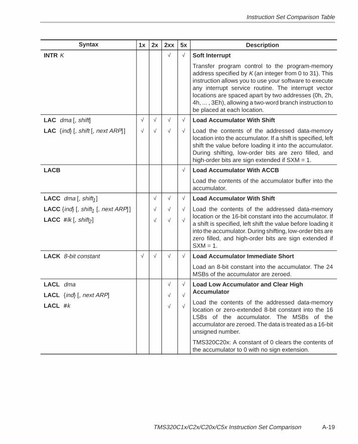
Instruction Set Comparison Table
A-19TMS320C1x/C2x/C20x/C5x Instruction Set Comparison
Syntax Description5x2xx2x1x
INTR K √ √ Soft Interrupt
Transfer program control to the program-memoryaddress specified by K (an integer from 0 to 31). Thisinstruction allows you to use your software to executeany interrupt service routine. The interrupt vectorlocations are spaced apart by two addresses (0h, 2h,4h, ... , 3Eh), allowing a two-word branch instruction tobe placed at each location.
LAC dma [, shift]
LAC ind [, shift [, next ARP] ]
√
√
√
√
√
√
√
√
Load Accumulator With Shift
Load the contents of the addressed data-memorylocation into the accumulator. If a shift is specified, leftshift the value before loading it into the accumulator.During shifting, low-order bits are zero filled, andhigh-order bits are sign extended if SXM = 1.
LACB √ Load Accumulator With ACCB
Load the contents of the accumulator buffer into theaccumulator.
LACC dma [, shift1]
LACC ind [, shift1 [, next ARP]]
LACC # lk [, shift2]
√
√
√
√
√
√
√
√
√
Load Accumulator With Shift
Load the contents of the addressed data-memorylocation or the 16-bit constant into the accumulator. Ifa shift is specified, left shift the value before loading itinto the accumulator. During shifting, low-order bits arezero filled, and high-order bits are sign extended ifSXM = 1.
LACK 8-bit constant √ √ √ √ Load Accumulator Immediate Short
Load an 8-bit constant into the accumulator. The 24MSBs of the accumulator are zeroed.
LACL dma
LACL ind [, next ARP]
LACL # k
√
√
√
√
√
√
Load Low Accumulator and Clear HighAccumulator
Load the contents of the addressed data-memorylocation or zero-extended 8-bit constant into the 16LSBs of the accumulator. The MSBs of theaccumulator are zeroed. The data is treated as a 16-bitunsigned number.
TMS320C20x: A constant of 0 clears the contents ofthe accumulator to 0 with no sign extension.
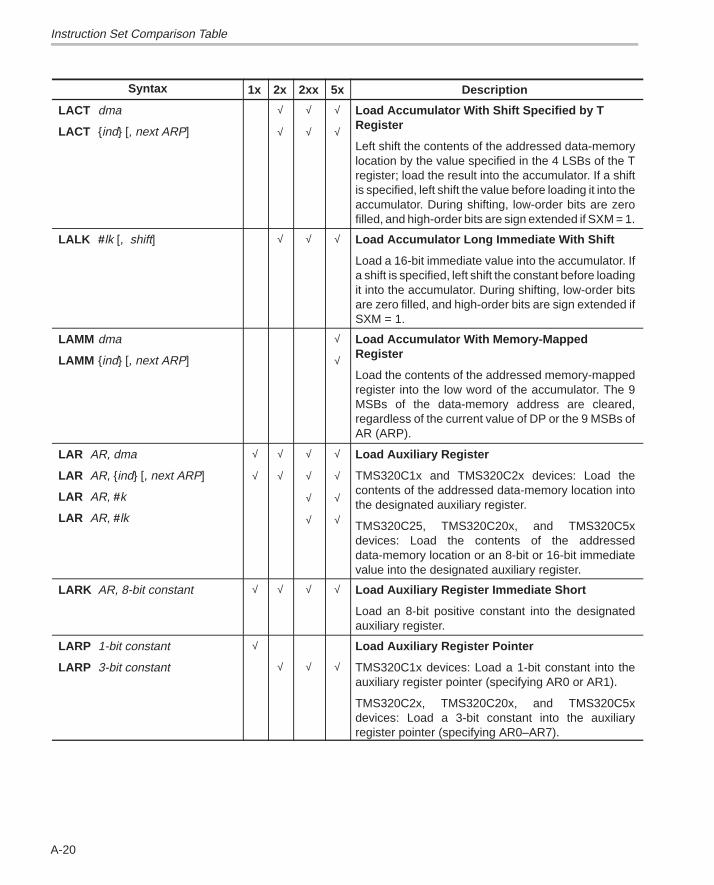
Instruction Set Comparison Table
A-20
Syntax Description5x2xx2x1x
LACT dma
LACT ind [, next ARP]
√
√
√
√
√
√
Load Accumulator With Shift Specified by TRegister
Left shift the contents of the addressed data-memorylocation by the value specified in the 4 LSBs of the Tregister; load the result into the accumulator. If a shiftis specified, left shift the value before loading it into theaccumulator. During shifting, low-order bits are zerofilled, and high-order bits are sign extended if SXM = 1.
LALK # lk [, shift] √ √ √ Load Accumulator Long Immediate With Shift
Load a 16-bit immediate value into the accumulator. Ifa shift is specified, left shift the constant before loadingit into the accumulator. During shifting, low-order bitsare zero filled, and high-order bits are sign extended ifSXM = 1.
LAMM dma
LAMM ind [, next ARP]
√
√
Load Accumulator With Memory-MappedRegister
Load the contents of the addressed memory-mappedregister into the low word of the accumulator. The 9MSBs of the data-memory address are cleared,regardless of the current value of DP or the 9 MSBs ofAR (ARP).
LAR AR, dma
LAR AR, ind [, next ARP]
LAR AR, #k
LAR AR, #lk
√
√
√
√
√
√
√
√
√
√
√
√
Load Auxiliary Register
TMS320C1x and TMS320C2x devices: Load thecontents of the addressed data-memory location intothe designated auxiliary register.
TMS320C25, TMS320C20x, and TMS320C5xdevices: Load the contents of the addresseddata-memory location or an 8-bit or 16-bit immediatevalue into the designated auxiliary register.
LARK AR, 8-bit constant √ √ √ √ Load Auxiliary Register Immediate Short
Load an 8-bit positive constant into the designatedauxiliary register.
LARP 1-bit constant
LARP 3-bit constant
√
√ √ √
Load Auxiliary Register Pointer
TMS320C1x devices: Load a 1-bit constant into theauxiliary register pointer (specifying AR0 or AR1).
TMS320C2x, TMS320C20x, and TMS320C5xdevices: Load a 3-bit constant into the auxiliaryregister pointer (specifying AR0–AR7).
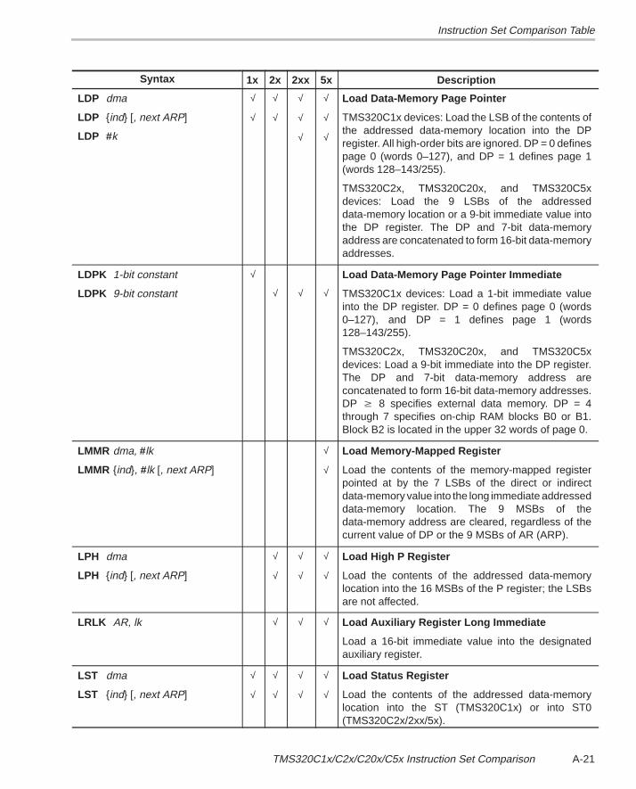
Instruction Set Comparison Table
A-21TMS320C1x/C2x/C20x/C5x Instruction Set Comparison
Syntax Description5x2xx2x1x
LDP dma
LDP ind [, next ARP]
LDP #k
√
√
√
√
√
√
√
√
√
√
Load Data-Memory Page Pointer
TMS320C1x devices: Load the LSB of the contents ofthe addressed data-memory location into the DPregister. All high-order bits are ignored. DP = 0 definespage 0 (words 0–127), and DP = 1 defines page 1(words 128–143/255).
TMS320C2x, TMS320C20x, and TMS320C5xdevices: Load the 9 LSBs of the addresseddata-memory location or a 9-bit immediate value intothe DP register. The DP and 7-bit data-memoryaddress are concatenated to form 16-bit data-memoryaddresses.
LDPK 1-bit constant
LDPK 9-bit constant
√
√ √ √
Load Data-Memory Page Pointer Immediate
TMS320C1x devices: Load a 1-bit immediate valueinto the DP register. DP = 0 defines page 0 (words0–127), and DP = 1 defines page 1 (words128–143/255).
TMS320C2x, TMS320C20x, and TMS320C5xdevices: Load a 9-bit immediate into the DP register.The DP and 7-bit data-memory address areconcatenated to form 16-bit data-memory addresses.DP 8 specifies external data memory. DP = 4through 7 specifies on-chip RAM blocks B0 or B1.Block B2 is located in the upper 32 words of page 0.
LMMR dma, #lk
LMMR ind, #lk [, next ARP]
√
√
Load Memory-Mapped Register
Load the contents of the memory-mapped registerpointed at by the 7 LSBs of the direct or indirectdata-memory value into the long immediate addresseddata-memory location. The 9 MSBs of thedata-memory address are cleared, regardless of thecurrent value of DP or the 9 MSBs of AR (ARP).
LPH dma
LPH ind [, next ARP]
√
√
√
√
√
√
Load High P Register
Load the contents of the addressed data-memorylocation into the 16 MSBs of the P register; the LSBsare not affected.
LRLK AR, lk √ √ √ Load Auxiliary Register Long Immediate
Load a 16-bit immediate value into the designatedauxiliary register.
LST dma
LST ind [, next ARP]
√
√
√
√
√
√
√
√
Load Status Register
Load the contents of the addressed data-memorylocation into the ST (TMS320C1x) or into ST0(TMS320C2x/2xx/5x).
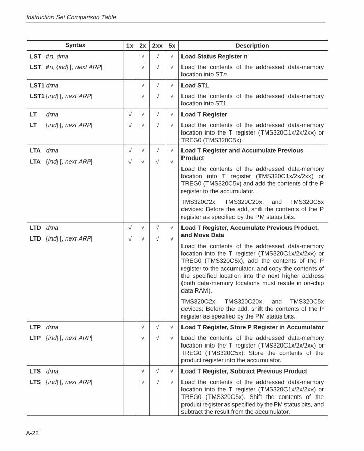
Instruction Set Comparison Table
A-22
Syntax Description5x2xx2x1x
LST #n, dma
LST #n, ind [, next ARP]
√
√
√
√
√
√
Load Status Register n
Load the contents of the addressed data-memorylocation into STn.
LST1 dma
LST1 ind [, next ARP]
√
√
√
√
√
√
Load ST1
Load the contents of the addressed data-memorylocation into ST1.
LT dma
LT ind [, next ARP]
√
√
√
√
√
√
√
√
Load T Register
Load the contents of the addressed data-memorylocation into the T register (TMS320C1x/2x/2xx) orTREG0 (TMS320C5x).
LTA dma
LTA ind [, next ARP]
√
√
√
√
√
√
√
√
Load T Register and Accumulate Previous Product
Load the contents of the addressed data-memorylocation into T register (TMS320C1x/2x/2xx) orTREG0 (TMS320C5x) and add the contents of the Pregister to the accumulator.
TMS320C2x, TMS320C20x, and TMS320C5xdevices: Before the add, shift the contents of the Pregister as specified by the PM status bits.
LTD dma
LTD ind [, next ARP]
√
√
√
√
√
√
√
√
Load T Register, Accumulate Previous Product,and Move Data
Load the contents of the addressed data-memorylocation into the T register (TMS320C1x/2x/2xx) orTREG0 (TMS320C5x), add the contents of the Pregister to the accumulator, and copy the contents ofthe specified location into the next higher address(both data-memory locations must reside in on-chipdata RAM).
TMS320C2x, TMS320C20x, and TMS320C5xdevices: Before the add, shift the contents of the Pregister as specified by the PM status bits.
LTP dma
LTP ind [, next ARP]
√
√
√
√
√
√
Load T Register, Store P Register in Accumulator
Load the contents of the addressed data-memorylocation into the T register (TMS320C1x/2x/2xx) orTREG0 (TMS320C5x). Store the contents of theproduct register into the accumulator.
LTS dma
LTS ind [, next ARP]
√
√
√
√
√
√
Load T Register, Subtract Previous Product
Load the contents of the addressed data-memorylocation into the T register (TMS320C1x/2x/2xx) orTREG0 (TMS320C5x). Shift the contents of theproduct register as specified by the PM status bits, andsubtract the result from the accumulator.
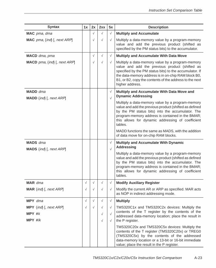
Instruction Set Comparison Table
A-23TMS320C1x/C2x/C20x/C5x Instruction Set Comparison
Syntax Description5x2xx2x1x
MAC pma, dma
MAC pma, ind [, next ARP]
√
√
√
√
√
√
Multiply and Accumulate
Multiply a data-memory value by a program-memoryvalue and add the previous product (shifted asspecified by the PM status bits) to the accumulator.
MACD dma, pma
MACD pma, ind [, next ARP]
√
√
√
√
√
√
Multiply and Accumulate With Data Move
Multiply a data-memory value by a program-memoryvalue and add the previous product (shifted asspecified by the PM status bits) to the accumulator. Ifthe data-memory address is in on-chip RAM block B0,B1, or B2, copy the contents of the address to the nexthigher address.
MADD dma
MADD ind [, next ARP]
√
√
Multiply and Accumulate With Data Move andDynamic Addressing
Multiply a data-memory value by a program-memoryvalue and add the previous product (shifted as definedby the PM status bits) into the accumulator. Theprogram-memory address is contained in the BMAR;this allows for dynamic addressing of coefficienttables.
MADD functions the same as MADS, with the additionof data move for on-chip RAM blocks.
MADS dma
MADS ind [, next ARP]
√
√
Multiply and Accumulate With DynamicAddressing
Multiply a data-memory value by a program-memoryvalue and add the previous product (shifted as definedby the PM status bits) into the accumulator. Theprogram-memory address is contained in the BMAR;this allows for dynamic addressing of coefficienttables.
MAR dma
MAR ind [, next ARP]
√
√
√
√
√
√
√
√
Modify Auxiliary Register
Modify the current AR or ARP as specified. MAR actsas NOP in indirect addressing mode.
MPY dma
MPY ind [, next ARP]
MPY #k
MPY #lk
√
√
√
√
√
√
√
√
√
√
√
√
Multiply
TMS320C1x and TMS320C2x devices: Multiply thecontents of the T register by the contents of theaddressed data-memory location; place the result inthe P register.
TMS320C20x and TMS320C5x devices: Multiply thecontents of the T register (TMS320C20x) or TREG0(TMS320C5x) by the contents of the addresseddata-memory location or a 13-bit or 16-bit immediatevalue; place the result in the P register.
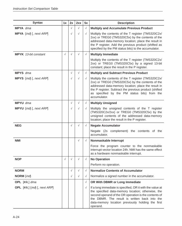
Instruction Set Comparison Table
A-24
Syntax Description5x2xx2x1x
MPYA dma
MPYA ind [, next ARP]
√
√
√
√
√
√
Multiply and Accumulate Previous Product
Multiply the contents of the T register (TMS320C2x/2xx) or TREG0 (TMS320C5x) by the contents of theaddressed data-memory location; place the result inthe P register. Add the previous product (shifted asspecified by the PM status bits) to the accumulator.
MPYK 13-bit constant √ √ √ √ Multiply Immediate
Multiply the contents of the T register (TMS320C2x/2xx) or TREG0 (TMS320C5x) by a signed 13-bitconstant; place the result in the P register.
MPYS dma
MPYS ind [, next ARP]
√
√
√
√
√
√
Multiply and Subtract Previous Product
Multiply the contents of the T register (TMS320C2x/2xx) or TREG0 (TMS320C5x) by the contents of theaddressed data-memory location; place the result inthe P register. Subtract the previous product (shiftedas specified by the PM status bits) from theaccumulator.
MPYU dma
MPYU ind [, next ARP]
√
√
√
√
√
√
Multiply Unsigned
Multiply the unsigned contents of the T register(TMS320C2x/2xx) or TREG0 (TMS320C5x) by theunsigned contents of the addressed data-memorylocation; place the result in the P register.
NEG √ √ √ Negate Accumulator
Negate (2s complement) the contents of theaccumulator.
NMI √ √ Nonmaskable Interrupt
Force the program counter to the nonmaskableinterrupt vector location 24h. NMI has the same effectas a hardware nonmaskable interrupt.
NOP √ √ √ √ No Operation
Perform no operation.
NORM
NORM ind
√
√
√
√
√
√
Normalize Contents of Accumulator
Normalize a signed number in the accumulator.
OPL [#lk,] dma
OPL [#lk,] ind [, next ARP]
√
√
OR With DBMR or Long Immediate
If a long immediate is specified, OR it with the value atthe specified data-memory location; otherwise, thesecond operand of the OR operation is the contents ofthe DBMR. The result is written back into thedata-memory location previously holding the firstoperand.
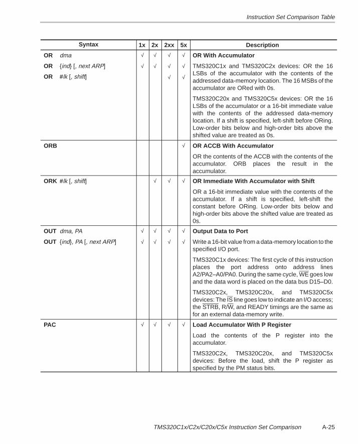
Instruction Set Comparison Table
A-25TMS320C1x/C2x/C20x/C5x Instruction Set Comparison
Syntax Description5x2xx2x1x
OR dma
OR ind [, next ARP]
OR #lk [, shift]
√
√
√
√
√
√
√
√
√
√
OR With Accumulator
TMS320C1x and TMS320C2x devices: OR the 16LSBs of the accumulator with the contents of theaddressed data-memory location. The 16 MSBs of theaccumulator are ORed with 0s.
TMS320C20x and TMS320C5x devices: OR the 16LSBs of the accumulator or a 16-bit immediate valuewith the contents of the addressed data-memorylocation. If a shift is specified, left-shift before ORing.Low-order bits below and high-order bits above theshifted value are treated as 0s.
ORB √ OR ACCB With Accumulator
OR the contents of the ACCB with the contents of theaccumulator. ORB places the result in theaccumulator.
ORK #lk [, shift] √ √ √ OR Immediate With Accumulator with Shift
OR a 16-bit immediate value with the contents of theaccumulator. If a shift is specified, left-shift theconstant before ORing. Low-order bits below andhigh-order bits above the shifted value are treated as0s.
OUT dma, PA
OUT ind, PA [, next ARP]
√
√
√
√
√
√
√
√
Output Data to Port
Write a 16-bit value from a data-memory location to thespecified I/O port.
TMS320C1x devices: The first cycle of this instructionplaces the port address onto address linesA2/PA2–A0/PA0. During the same cycle, WE goes lowand the data word is placed on the data bus D15–D0.
TMS320C2x, TMS320C20x, and TMS320C5xdevices: The IS line goes low to indicate an I/O access;the STRB, R/W, and READY timings are the same asfor an external data-memory write.
PAC √ √ √ √ Load Accumulator With P Register
Load the contents of the P register into theaccumulator.
TMS320C2x, TMS320C20x, and TMS320C5xdevices: Before the load, shift the P register asspecified by the PM status bits.
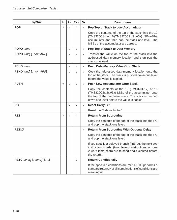
Instruction Set Comparison Table
A-26
Syntax Description5x2xx2x1x
POP √ √ √ √ Pop Top of Stack to Low Accumulator
Copy the contents of the top of the stack into the 12(TMS320C1x) or 16 (TMS320C2x/2xx/5x) LSBs of theaccumulator and then pop the stack one level. TheMSBs of the accumulator are zeroed.
POPD dma
POPD ind [, next ARP]
√
√
√
√
√
√
Pop Top of Stack to Data Memory
Transfer the value on the top of the stack into theaddressed data-memory location and then pop thestack one level.
PSHD dma
PSHD ind [, next ARP]
√
√
√
√
√
√
Push Data-Memory Value Onto Stack
Copy the addressed data-memory location onto thetop of the stack. The stack is pushed down one levelbefore the value is copied.
PUSH √ √ √ √ Push Low Accumulator Onto Stack
Copy the contents of the 12 (TMS320C1x) or 16(TMS320C2x/2xx/5x) LSBs of the accumulator ontothe top of the hardware stack. The stack is pusheddown one level before the value is copied.
RC √ √ √ Reset Carry Bit
Reset the C status bit to 0.
RET √ √ √ Return From Subroutine
Copy the contents of the top of the stack into the PCand pop the stack one level.
RET[D] √ Return From Subroutine With Optional Delay
Copy the contents of the top of the stack into the PCand pop the stack one level.
If you specify a delayed branch (RETD), the next twoinstruction words (two 1-word instructions or one2-word instruction) are fetched and executed beforethe return.
RETC cond1 [, cond2] [, ...] √ Return Conditionally
If the specified conditions are met, RETC performs astandard return. Not all combinations of conditions aremeaningful.
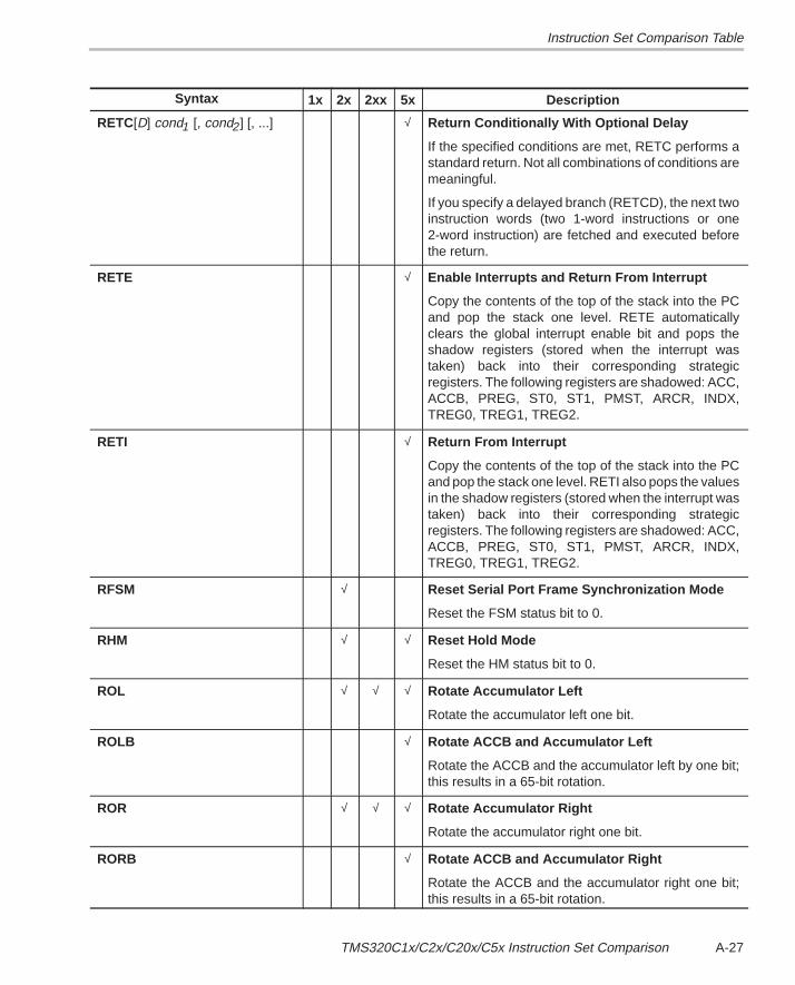
Instruction Set Comparison Table
A-27TMS320C1x/C2x/C20x/C5x Instruction Set Comparison
Syntax Description5x2xx2x1x
RETC[D] cond1 [, cond2] [, ...] √ Return Conditionally With Optional Delay
If the specified conditions are met, RETC performs astandard return. Not all combinations of conditions aremeaningful.
If you specify a delayed branch (RETCD), the next twoinstruction words (two 1-word instructions or one2-word instruction) are fetched and executed beforethe return.
RETE √ Enable Interrupts and Return From Interrupt
Copy the contents of the top of the stack into the PCand pop the stack one level. RETE automaticallyclears the global interrupt enable bit and pops theshadow registers (stored when the interrupt wastaken) back into their corresponding strategicregisters. The following registers are shadowed: ACC,ACCB, PREG, ST0, ST1, PMST, ARCR, INDX,TREG0, TREG1, TREG2.
RETI √ Return From Interrupt
Copy the contents of the top of the stack into the PCand pop the stack one level. RETI also pops the valuesin the shadow registers (stored when the interrupt wastaken) back into their corresponding strategicregisters. The following registers are shadowed: ACC,ACCB, PREG, ST0, ST1, PMST, ARCR, INDX,TREG0, TREG1, TREG2.
RFSM √ Reset Serial Port Frame Synchronization Mode
Reset the FSM status bit to 0.
RHM √ √ Reset Hold Mode
Reset the HM status bit to 0.
ROL √ √ √ Rotate Accumulator Left
Rotate the accumulator left one bit.
ROLB √ Rotate ACCB and Accumulator Left
Rotate the ACCB and the accumulator left by one bit;this results in a 65-bit rotation.
ROR √ √ √ Rotate Accumulator Right
Rotate the accumulator right one bit.
RORB √ Rotate ACCB and Accumulator Right
Rotate the ACCB and the accumulator right one bit;this results in a 65-bit rotation.
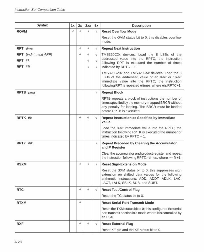
Instruction Set Comparison Table
A-28
Syntax Description5x2xx2x1x
ROVM √ √ √ √ Reset Overflow Mode
Reset the OVM status bit to 0; this disables overflowmode.
RPT dma
RPT ind [, next ARP]
RPT #k
RPT #lk
√
√
√
√
√
√
√
√
√
√
Repeat Next Instruction
TMS320C2x devices: Load the 8 LSBs of theaddressed value into the RPTC; the instructionfollowing RPT is executed the number of timesindicated by RPTC + 1.
TMS320C20x and TMS320C5x devices: Load the 8LSBs of the addressed value or an 8-bit or 16-bitimmediate value into the RPTC; the instructionfollowing RPT is repeated n times, where n is RPTC+1.
RPTB pma √ Repeat Block
RPTB repeats a block of instructions the number oftimes specified by the memory-mapped BRCR withoutany penalty for looping. The BRCR must be loadedbefore RPTB is executed.
RPTK #k √ √ √ Repeat Instruction as Specified by ImmediateValue
Load the 8-bit immediate value into the RPTC; theinstruction following RPTK is executed the number oftimes indicated by RPTC + 1.
RPTZ #lk √ Repeat Preceded by Clearing the Accumulatorand P Register
Clear the accumulator and product register and repeatthe instruction following RPTZ n times, where n = lk +1.
RSXM √ √ √ Reset Sign-Extension Mode
Reset the SXM status bit to 0; this suppresses signextension on shifted data values for the followingarithmetic instructions: ADD, ADDT, ADLK, LAC,LACT, LALK, SBLK, SUB, and SUBT.
RTC √ √ √ Reset Test/Control Flag
Reset the TC status bit to 0.
RTXM √ Reset Serial Port Transmit Mode
Reset the TXM status bit to 0; this configures the serialport transmit section in a mode where it is controlled byan FSX.
RXF √ √ √ Reset External Flag
Reset XF pin and the XF status bit to 0.
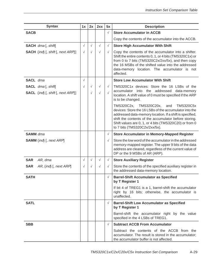
Instruction Set Comparison Table
A-29TMS320C1x/C2x/C20x/C5x Instruction Set Comparison
Syntax Description5x2xx2x1x
SACB √ Store Accumulator in ACCB
Copy the contents of the accumulator into the ACCB.
SACH dma [, shift]
SACH ind [, shift [, next ARP] ]
√
√
√
√
√
√
√
√
Store High Accumulator With Shift
Copy the contents of the accumulator into a shifter.Shift the entire contents 0, 1, or 4 bits (TMS320C1x) orfrom 0 to 7 bits (TMS320C2x/2xx/5x), and then copythe 16 MSBs of the shifted value into the addresseddata-memory location. The accumulator is notaffected.
SACL dma
SACL dma [, shift]
SACL ind [, shift [, next ARP] ]
√
√ √
√
√
√
√
√
Store Low Accumulator With Shift
TMS320C1x devices: Store the 16 LSBs of theaccumulator into the addressed data-memorylocation. A shift value of 0 must be specified if the ARPis to be changed.
TMS320C2x, TMS320C20x, and TMS320C5xdevices: Store the 16 LSBs of the accumulator into theaddressed data-memory location. If a shift is specified,shift the contents of the accumulator before storing.Shift values are 0, 1, or 4 bits (TMS320C20) or from 0to 7 bits (TMS320C2x/2xx/5x).
SAMM dma
SAMM ind [, next ARP]
√
√
Store Accumulator in Memory-Mapped Register
Store the low word of the accumulator in the addressedmemory-mapped register. The upper 9 bits of the dataaddress are cleared, regardless of the current value ofDP or the 9 MSBs of AR (ARP).
SAR AR, dma
SAR AR, ind [, next ARP]
√
√
√
√
√
√
√
√
Store Auxiliary Register
Store the contents of the specified auxiliary register inthe addressed data-memory location.
SATH √ Barrel-Shift Accumulator as Specified by T Register 1
If bit 4 of TREG1 is a 1, barrel-shift the accumulatorright by 16 bits; otherwise, the accumulator isunaffected.
SATL √ Barrel-Shift Low Accumulator as Specified by T Register 1
Barrel-shift the accumulator right by the valuespecified in the 4 LSBs of TREG1.
SBB √ Subtract ACCB From Accumulator
Subtract the contents of the ACCB from theaccumulator. The result is stored in the accumulator;the accumulator buffer is not affected.
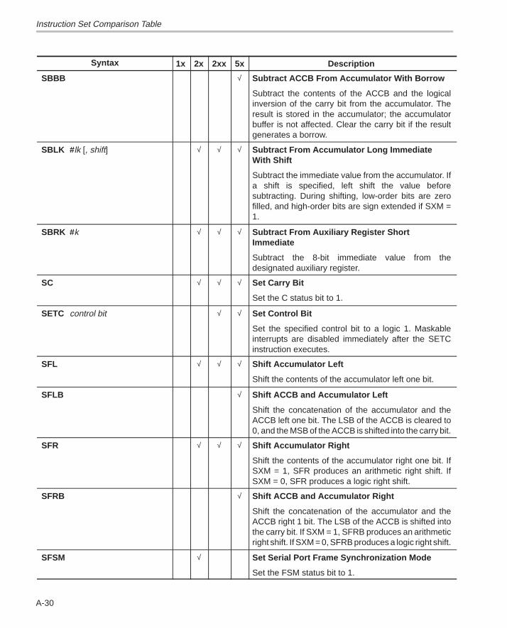
Instruction Set Comparison Table
A-30
Syntax Description5x2xx2x1x
SBBB √ Subtract ACCB From Accumulator With Borrow
Subtract the contents of the ACCB and the logicalinversion of the carry bit from the accumulator. Theresult is stored in the accumulator; the accumulatorbuffer is not affected. Clear the carry bit if the resultgenerates a borrow.
SBLK # lk [, shift] √ √ √ Subtract From Accumulator Long ImmediateWith Shift
Subtract the immediate value from the accumulator. Ifa shift is specified, left shift the value beforesubtracting. During shifting, low-order bits are zerofilled, and high-order bits are sign extended if SXM =1.
SBRK #k √ √ √ Subtract From Auxiliary Register ShortImmediate
Subtract the 8-bit immediate value from thedesignated auxiliary register.
SC √ √ √ Set Carry Bit
Set the C status bit to 1.
SETC control bit √ √ Set Control Bit
Set the specified control bit to a logic 1. Maskableinterrupts are disabled immediately after the SETCinstruction executes.
SFL √ √ √ Shift Accumulator Left
Shift the contents of the accumulator left one bit.
SFLB √ Shift ACCB and Accumulator Left
Shift the concatenation of the accumulator and theACCB left one bit. The LSB of the ACCB is cleared to0, and the MSB of the ACCB is shifted into the carry bit.
SFR √ √ √ Shift Accumulator Right
Shift the contents of the accumulator right one bit. IfSXM = 1, SFR produces an arithmetic right shift. IfSXM = 0, SFR produces a logic right shift.
SFRB √ Shift ACCB and Accumulator Right
Shift the concatenation of the accumulator and theACCB right 1 bit. The LSB of the ACCB is shifted intothe carry bit. If SXM = 1, SFRB produces an arithmeticright shift. If SXM = 0, SFRB produces a logic right shift.
SFSM √ Set Serial Port Frame Synchronization Mode
Set the FSM status bit to 1.
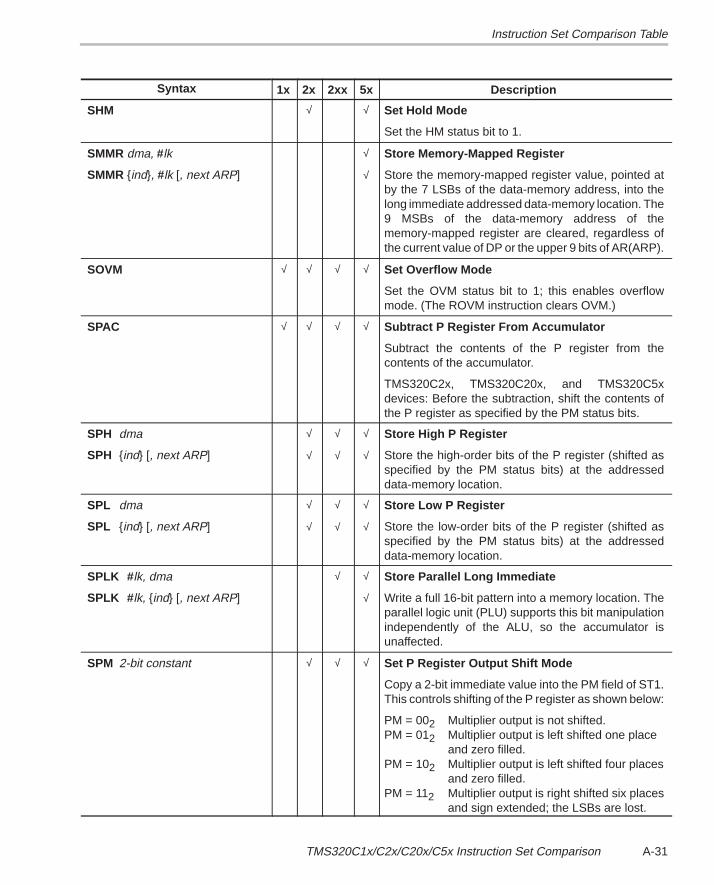
Instruction Set Comparison Table
A-31TMS320C1x/C2x/C20x/C5x Instruction Set Comparison
Syntax Description5x2xx2x1x
SHM √ √ Set Hold Mode
Set the HM status bit to 1.
SMMR dma, #lk
SMMR ind, #lk [, next ARP]
√
√
Store Memory-Mapped Register
Store the memory-mapped register value, pointed atby the 7 LSBs of the data-memory address, into thelong immediate addressed data-memory location. The9 MSBs of the data-memory address of thememory-mapped register are cleared, regardless ofthe current value of DP or the upper 9 bits of AR(ARP).
SOVM √ √ √ √ Set Overflow Mode
Set the OVM status bit to 1; this enables overflowmode. (The ROVM instruction clears OVM.)
SPAC √ √ √ √ Subtract P Register From Accumulator
Subtract the contents of the P register from thecontents of the accumulator.
TMS320C2x, TMS320C20x, and TMS320C5xdevices: Before the subtraction, shift the contents ofthe P register as specified by the PM status bits.
SPH dma
SPH ind [, next ARP]
√
√
√
√
√
√
Store High P Register
Store the high-order bits of the P register (shifted asspecified by the PM status bits) at the addresseddata-memory location.
SPL dma
SPL ind [, next ARP]
√
√
√
√
√
√
Store Low P Register
Store the low-order bits of the P register (shifted asspecified by the PM status bits) at the addresseddata-memory location.
SPLK # lk, dma
SPLK # lk, ind [, next ARP]
√ √
√
Store Parallel Long Immediate
Write a full 16-bit pattern into a memory location. Theparallel logic unit (PLU) supports this bit manipulationindependently of the ALU, so the accumulator isunaffected.
SPM 2-bit constant √ √ √ Set P Register Output Shift Mode
Copy a 2-bit immediate value into the PM field of ST1.This controls shifting of the P register as shown below:
PM = 002 Multiplier output is not shifted.PM = 012 Multiplier output is left shifted one place
and zero filled.PM = 102 Multiplier output is left shifted four places and zero filled.PM = 112 Multiplier output is right shifted six places
and sign extended; the LSBs are lost.
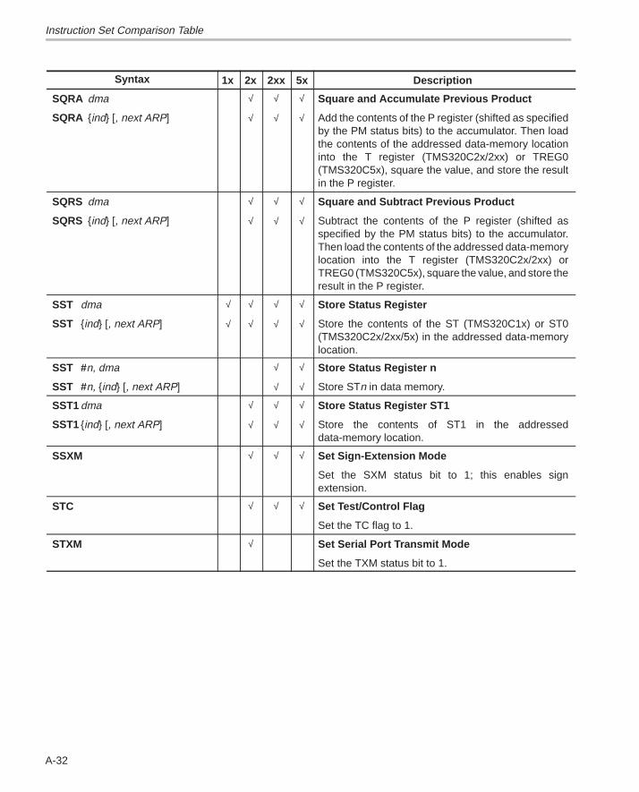
Instruction Set Comparison Table
A-32
Syntax Description5x2xx2x1x
SQRA dma
SQRA ind [, next ARP]
√
√
√
√
√
√
Square and Accumulate Previous Product
Add the contents of the P register (shifted as specifiedby the PM status bits) to the accumulator. Then loadthe contents of the addressed data-memory locationinto the T register (TMS320C2x/2xx) or TREG0(TMS320C5x), square the value, and store the resultin the P register.
SQRS dma
SQRS ind [, next ARP]
√
√
√
√
√
√
Square and Subtract Previous Product
Subtract the contents of the P register (shifted asspecified by the PM status bits) to the accumulator.Then load the contents of the addressed data-memorylocation into the T register (TMS320C2x/2xx) orTREG0 (TMS320C5x), square the value, and store theresult in the P register.
SST dma
SST ind [, next ARP]
√
√
√
√
√
√
√
√
Store Status Register
Store the contents of the ST (TMS320C1x) or ST0(TMS320C2x/2xx/5x) in the addressed data-memorylocation.
SST #n, dma
SST #n, ind [, next ARP]
√
√
√
√
Store Status Register n
Store STn in data memory.
SST1 dma
SST1 ind [, next ARP]
√
√
√
√
√
√
Store Status Register ST1
Store the contents of ST1 in the addresseddata-memory location.
SSXM √ √ √ Set Sign-Extension Mode
Set the SXM status bit to 1; this enables signextension.
STC √ √ √ Set Test/Control Flag
Set the TC flag to 1.
STXM √ Set Serial Port Transmit Mode
Set the TXM status bit to 1.
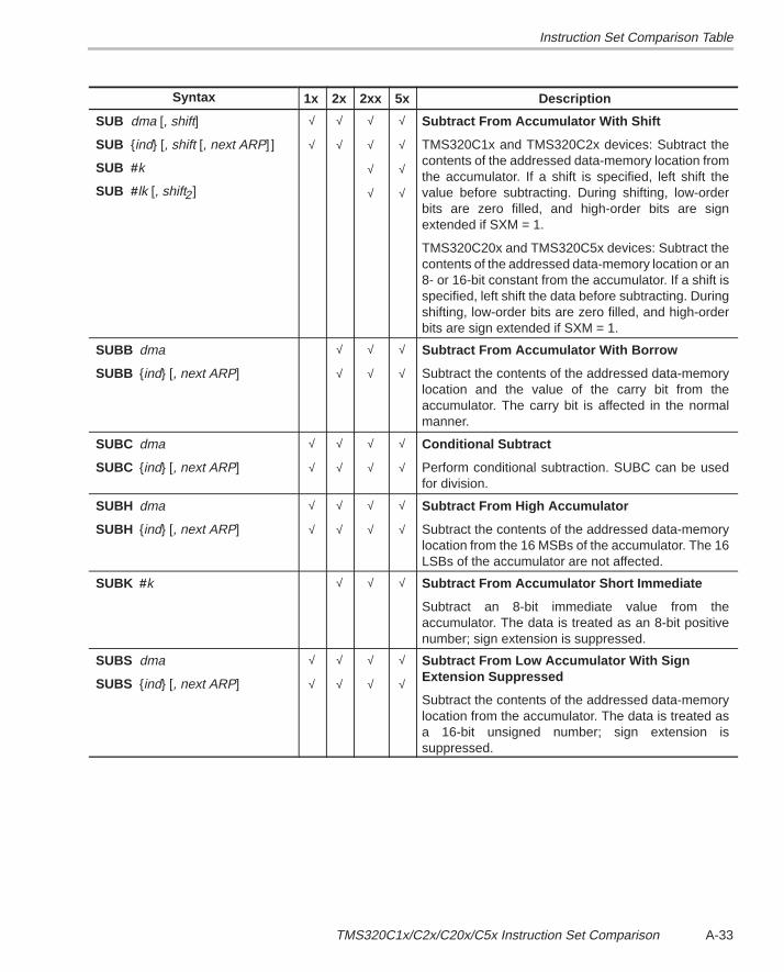
Instruction Set Comparison Table
A-33TMS320C1x/C2x/C20x/C5x Instruction Set Comparison
Syntax Description5x2xx2x1x
SUB dma [, shift]
SUB ind [, shift [, next ARP] ]
SUB #k
SUB #lk [, shift2]
√
√
√
√
√
√
√
√
√
√
√
√
Subtract From Accumulator With Shift
TMS320C1x and TMS320C2x devices: Subtract thecontents of the addressed data-memory location fromthe accumulator. If a shift is specified, left shift thevalue before subtracting. During shifting, low-orderbits are zero filled, and high-order bits are signextended if SXM = 1.
TMS320C20x and TMS320C5x devices: Subtract thecontents of the addressed data-memory location or an8- or 16-bit constant from the accumulator. If a shift isspecified, left shift the data before subtracting. Duringshifting, low-order bits are zero filled, and high-orderbits are sign extended if SXM = 1.
SUBB dma
SUBB ind [, next ARP]
√
√
√
√
√
√
Subtract From Accumulator With Borrow
Subtract the contents of the addressed data-memorylocation and the value of the carry bit from theaccumulator. The carry bit is affected in the normalmanner.
SUBC dma
SUBC ind [, next ARP]
√
√
√
√
√
√
√
√
Conditional Subtract
Perform conditional subtraction. SUBC can be usedfor division.
SUBH dma
SUBH ind [, next ARP]
√
√
√
√
√
√
√
√
Subtract From High Accumulator
Subtract the contents of the addressed data-memorylocation from the 16 MSBs of the accumulator. The 16LSBs of the accumulator are not affected.
SUBK #k √ √ √ Subtract From Accumulator Short Immediate
Subtract an 8-bit immediate value from theaccumulator. The data is treated as an 8-bit positivenumber; sign extension is suppressed.
SUBS dma
SUBS ind [, next ARP]
√
√
√
√
√
√
√
√
Subtract From Low Accumulator With SignExtension Suppressed
Subtract the contents of the addressed data-memorylocation from the accumulator. The data is treated asa 16-bit unsigned number; sign extension issuppressed.
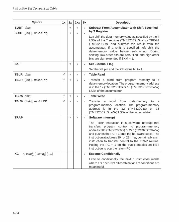
Instruction Set Comparison Table
A-34
Syntax Description5x2xx2x1x
SUBT dma
SUBT ind [, next ARP]
√
√
√
√
√
√
Subtract From Accumulator With Shift Specifiedby T Register
Left shift the data-memory value as specified by the 4LSBs of the T register (TMS320C2x/2xx) or TREG1(TMS320C5x), and subtract the result from theaccumulator. If a shift is specified, left shift thedata-memory value before subtracting. Duringshifting, low-order bits are zero filled, and high-orderbits are sign extended if SXM = 1.
SXF √ √ √ Set External Flag
Set the XF pin and the XF status bit to 1.
TBLR dma
TBLR ind [, next ARP]
√
√
√
√
√
√
√
√
Table Read
Transfer a word from program memory to adata-memory location. The program-memory addressis in the 12 (TMS320C1x) or 16 (TMS320C2x/2xx/5x)LSBs of the accumulator.
TBLW dma
TBLW ind [, next ARP]
√
√
√
√
√
√
√
√
Table Write
Transfer a word from data-memory to aprogram-memory location. The program-memoryaddress is in the 12 (TMS320C1x) or 16(TMS320C2x/2xx/5x) LSBs of the accumulator.
TRAP √ √ √ Software Interrupt
The TRAP instruction is a software interrupt thattransfers program control to program-memoryaddress 30h (TMS320C2x) or 22h (TMS320C20x/5x)and pushes the PC + 1 onto the hardware stack. Theinstruction at address 30h or 22h may contain a branchinstruction to transfer control to the TRAP routine.Putting the PC + 1 on the stack enables an RETinstruction to pop the return PC.
XC n, cond1 [, cond2] [, ...] √ Execute Conditionally
Execute conditionally the next n instruction wordswhere 1 ≤ n ≤ 2. Not all combinations of conditions aremeaningful.
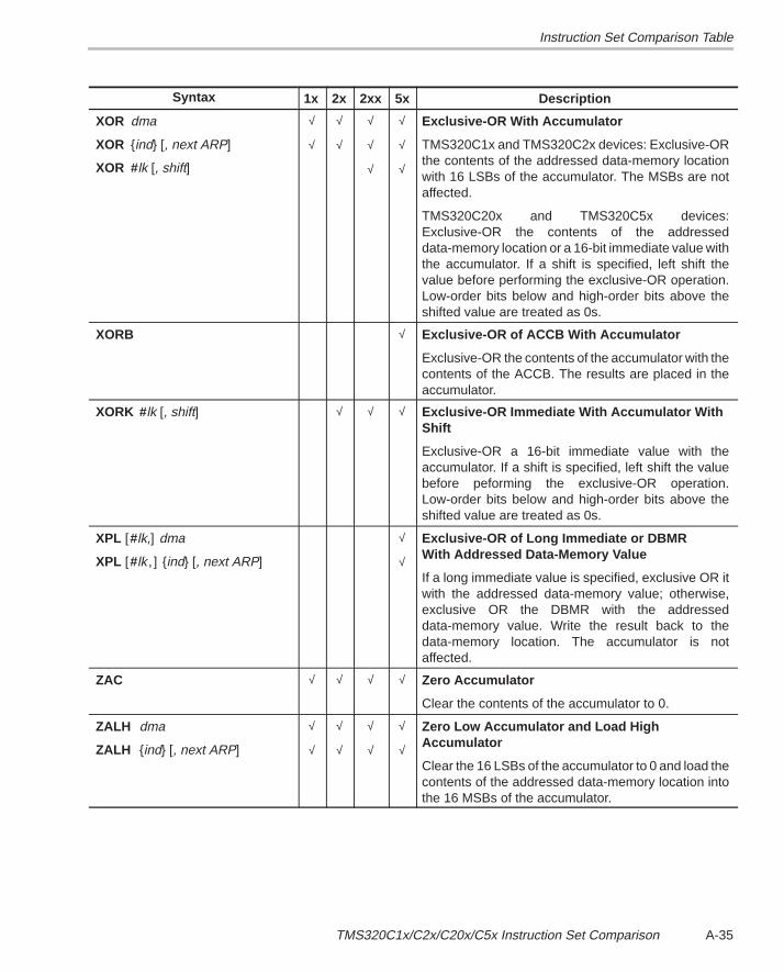
Instruction Set Comparison Table
A-35TMS320C1x/C2x/C20x/C5x Instruction Set Comparison
Syntax Description5x2xx2x1x
XOR dma
XOR ind [, next ARP]
XOR #lk [, shift]
√
√
√
√
√
√
√
√
√
√
Exclusive-OR With Accumulator
TMS320C1x and TMS320C2x devices: Exclusive-ORthe contents of the addressed data-memory locationwith 16 LSBs of the accumulator. The MSBs are notaffected.
TMS320C20x and TMS320C5x devices:Exclusive-OR the contents of the addresseddata-memory location or a 16-bit immediate value withthe accumulator. If a shift is specified, left shift thevalue before performing the exclusive-OR operation.Low-order bits below and high-order bits above theshifted value are treated as 0s.
XORB √ Exclusive-OR of ACCB With Accumulator
Exclusive-OR the contents of the accumulator with thecontents of the ACCB. The results are placed in theaccumulator.
XORK #lk [, shift] √ √ √ Exclusive-OR Immediate With Accumulator WithShift
Exclusive-OR a 16-bit immediate value with theaccumulator. If a shift is specified, left shift the valuebefore peforming the exclusive-OR operation.Low-order bits below and high-order bits above theshifted value are treated as 0s.
XPL [#lk,] dma
XPL [#lk , ] ind [, next ARP]
√
√
Exclusive-OR of Long Immediate or DBMR With Addressed Data-Memory Value
If a long immediate value is specified, exclusive OR itwith the addressed data-memory value; otherwise,exclusive OR the DBMR with the addresseddata-memory value. Write the result back to thedata-memory location. The accumulator is notaffected.
ZAC √ √ √ √ Zero Accumulator
Clear the contents of the accumulator to 0.
ZALH dma
ZALH ind [, next ARP]
√
√
√
√
√
√
√
√
Zero Low Accumulator and Load High Accumulator
Clear the 16 LSBs of the accumulator to 0 and load thecontents of the addressed data-memory location intothe 16 MSBs of the accumulator.
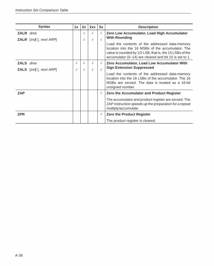
Instruction Set Comparison Table
A-36
Syntax Description5x2xx2x1x
ZALR dma
ZALR ind [, next ARP]
√
√
√
√
√
√
Zero Low Accumulator, Load High AccumulatorWith Rounding
Load the contents of the addressed data-memorylocation into the 16 MSBs of the accumulator. Thevalue is rounded by 1/2 LSB; that is, the 15 LSBs of theaccumulator (0–14) are cleared and bit 15 is set to 1.
ZALS dma
ZALS ind [, next ARP]
√
√
√
√
√
√
√
√
Zero Accumulator, Load Low Accumulator WithSign Extension Suppressed
Load the contents of the addressed data-memorylocation into the 16 LSBs of the accumulator. The 16MSBs are zeroed. The data is treated as a 16-bitunsigned number.
ZAP √ Zero the Accumulator and Product Register
The accumulator and product register are zeroed. TheZAP instruction speeds up the preparation for a repeatmultiply/accumulate.
ZPR √ Zero the Product Register
The product register is cleared.
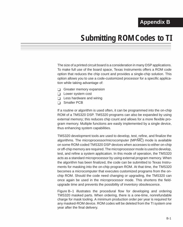
B-1
Appendix A
Submitting ROM Codes to TI
The size of a printed circuit board is a consideration in many DSP applications.To make full use of the board space, Texas Instruments offers a ROM codeoption that reduces the chip count and provides a single-chip solution. Thisoption allows you to use a code-customized processor for a specific applica-tion while taking advantage of:
Greater memory expansion Lower system cost Less hardware and wiring Smaller PCB
If a routine or algorithm is used often, it can be programmed into the on-chipROM of a TMS320 DSP. TMS320 programs can also be expanded by usingexternal memory; this reduces chip count and allows for a more flexible pro-gram memory. Multiple functions are easily implemented by a single device,thus enhancing system capabilities.
TMS320 development tools are used to develop, test, refine, and finalize thealgorithms. The microprocessor/microcomputer (MP/MC) mode is availableon some ROM-coded TMS320 DSP devices when accesses to either on-chipor off-chip memory are required. The microprocessor mode is used to develop,test, and refine a system application. In this mode of operation, the TMS320acts as a standard microprocessor by using external program memory. Whenthe algorithm has been finalized, the code can be submitted to Texas Instru-ments for masking into the on-chip program ROM. At that time, the TMS320becomes a microcomputer that executes customized programs from the on-chip ROM. Should the code need changing or upgrading, the TMS320 canonce again be used in the microprocessor mode. This shortens the field-upgrade time and prevents the possibility of inventory obsolescence.
Figure B–1 illustrates the procedural flow for developing and orderingTMS320 masked parts. When ordering, there is a one-time, nonrefundablecharge for mask tooling. A minimum production order per year is required forany masked-ROM device. ROM codes will be deleted from the TI system oneyear after the final delivery.
Appendix B
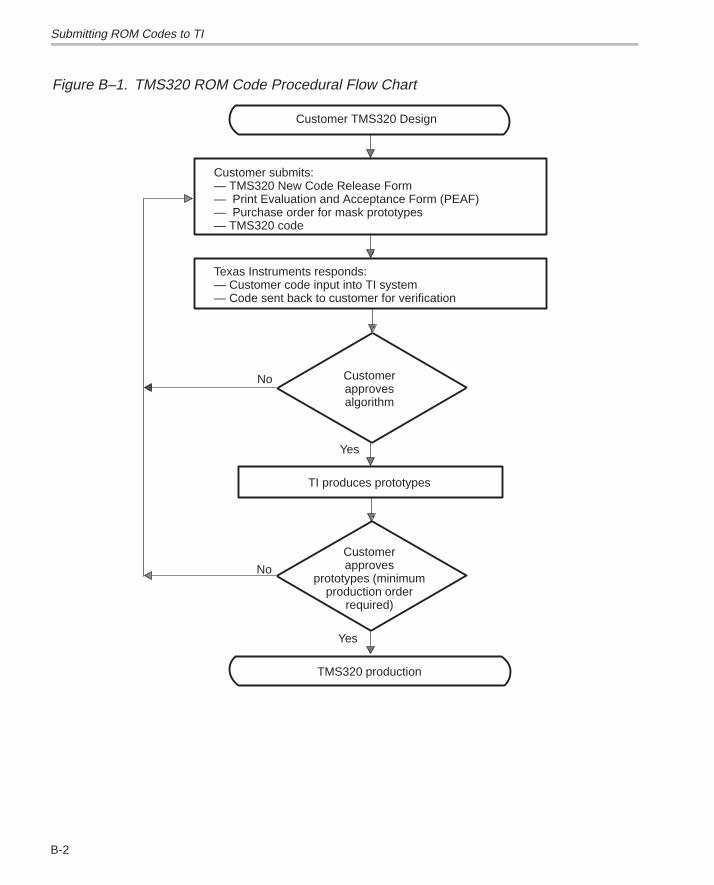
Submitting ROM Codes to TI
B-2
Figure B–1. TMS320 ROM Code Procedural Flow Chart
Customer TMS320 Design
Customer submits:— TMS320 New Code Release Form— Print Evaluation and Acceptance Form (PEAF)— Purchase order for mask prototypes— TMS320 code
Texas Instruments responds:— Customer code input into TI system— Code sent back to customer for verification
Customerapprovesalgorithm
TI produces prototypes
Customerapproves
prototypes (minimumproduction order
required)
TMS320 production
Yes
Yes
No
No
Submitting ROM Codes to TI
B-3Submitting ROM Codes to TI
The TMS320 ROM code may be submitted in one of the following forms:
Attachment to e–mail
3-1/2-in floppy: COFF format from macro-assembler/linker
When code is submitted to TI for masking, the code is reformatted to accom-modate the TI mask-generation system. System-level verification by the cus-tomer is, therefore, necessary to ensure the reformatting remains transparentand does not affect the execution of the algorithm. The formatting changesinvolve the removal of address-relocation information (the code addressbegins at the base address of the ROM in the TMS320 device and progresseswithout gaps to the last address of the ROM) and the addition of data in thereserved locations of the ROM for device ROM test. Because these changeshave been made, a checksum comparison is not a valid means of verification.
With each masked-device order, the customer must sign a disclaimer thatstates:
The units to be shipped against this order were assembled, for expe-diency purposes, on a prototype (that is, nonproduction qualified)manufacturing line, the reliability of which is not fully characterized.Therefore, the anticipated inherent reliability of these prototype unitscannot be expressly defined.
and a release that states:
Any masked ROM device may be resymbolized as TI standardproduct and resold as though it were an unprogrammed version ofthe device, at the convenience of Texas Instruments.
The use of the ROM-protect feature does not hold for this release statement.Additional risk and charges are involved when the ROM-protect feature isselected. Contact the nearest TI Field Sales Office for more information onprocedures, leadtimes, and cost associated with the ROM-protect feature.
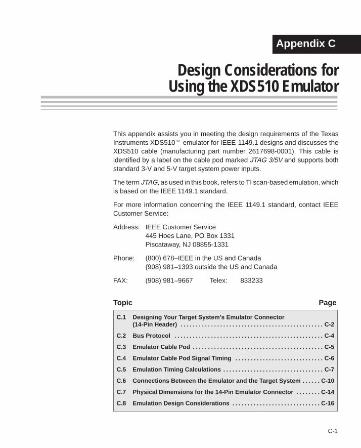
C-1
Appendix A
Design Considerations forUsing the XDS510 Emulator
This appendix assists you in meeting the design requirements of the TexasInstruments XDS510 emulator for IEEE-1149.1 designs and discusses theXDS510 cable (manufacturing part number 2617698-0001). This cable isidentified by a label on the cable pod marked JTAG 3/5V and supports bothstandard 3-V and 5-V target system power inputs.
The term JTAG, as used in this book, refers to TI scan-based emulation, whichis based on the IEEE 1149.1 standard.
For more information concerning the IEEE 1149.1 standard, contact IEEECustomer Service:
Address: IEEE Customer Service445 Hoes Lane, PO Box 1331Piscataway, NJ 08855-1331
Phone: (800) 678–IEEE in the US and Canada(908) 981–1393 outside the US and Canada
FAX: (908) 981–9667 Telex: 833233
Topic Page
C.1 Designing Your Target System’s Emulator Connector(14-Pin Header) C-2. . . . . . . . . . . . . . . . . . . . . . . . . . . . . . . . . . . . . . . . . . . . . . .
C.2 Bus Protocol C-4. . . . . . . . . . . . . . . . . . . . . . . . . . . . . . . . . . . . . . . . . . . . . . . . .
C.3 Emulator Cable Pod C-5. . . . . . . . . . . . . . . . . . . . . . . . . . . . . . . . . . . . . . . . . . .
C.4 Emulator Cable Pod Signal Timing C-6. . . . . . . . . . . . . . . . . . . . . . . . . . . . .
C.5 Emulation Timing Calculations C-7. . . . . . . . . . . . . . . . . . . . . . . . . . . . . . . . .
C.6 Connections Between the Emulator and the Target System C-10. . . . . .
C.7 Physical Dimensions for the 14-Pin Emulator Connector C-14. . . . . . . .
C.8 Emulation Design Considerations C-16. . . . . . . . . . . . . . . . . . . . . . . . . . . . .
Appendix C
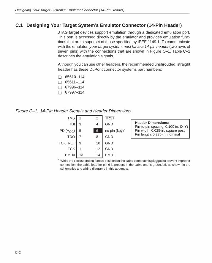
Designing Your Target System’s Emulator Connector (14-Pin Header)
C-2
C.1 Designing Your Target System’s Emulator Connector (14-Pin Header)JTAG target devices support emulation through a dedicated emulation port.This port is accessed directly by the emulator and provides emulation func-tions that are a superset of those specified by IEEE 1149.1. To communicatewith the emulator, your target system must have a 14-pin header (two rows ofseven pins) with the connections that are shown in Figure C–1. Table C–1describes the emulation signals.
Although you can use other headers, the recommended unshrouded, straightheader has these DuPont connector systems part numbers:
65610–114 65611–114 67996–114 67997–114
Figure C–1. 14-Pin Header Signals and Header Dimensions
TDI 3 4 GND
TDO 7 8 GND
TMS 1 2 TRST
TCK_RET 9 10 GND
TCK 11 12 GND
Header Dimensions:Pin-to-pin spacing, 0.100 in. (X,Y)Pin width, 0.025-in. square postPin length, 0.235-in. nominal
PD (VCC) 5 6 no pin (key)†
EMU0 13 14 EMU1† While the corresponding female position on the cable connector is plugged to prevent improper
connection, the cable lead for pin 6 is present in the cable and is grounded, as shown in theschematics and wiring diagrams in this appendix.
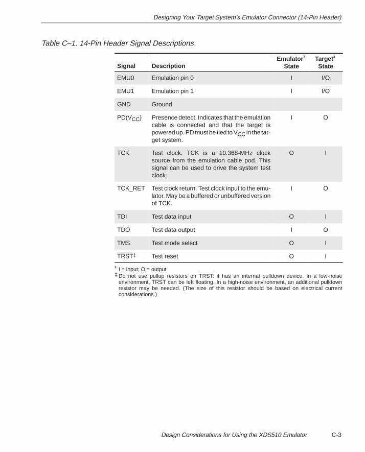
Designing Your Target System’s Emulator Connector (14-Pin Header)
C-3Design Considerations for Using the XDS510 Emulator
Table C–1. 14-Pin Header Signal Descriptions
Signal DescriptionEmulator †
StateTarget †
State
EMU0 Emulation pin 0 I I/O
EMU1 Emulation pin 1 I I/O
GND Ground
PD(VCC) Presence detect. Indicates that the emulationcable is connected and that the target ispowered up. PD must be tied to VCC in the tar-get system.
I O
TCK Test clock. TCK is a 10.368-MHz clocksource from the emulation cable pod. Thissignal can be used to drive the system testclock.
O I
TCK_RET Test clock return. Test clock input to the emu-lator. May be a buffered or unbuffered versionof TCK.
I O
TDI Test data input O I
TDO Test data output I O
TMS Test mode select O I
TRST‡ Test reset O I
† I = input; O = output‡ Do not use pullup resistors on TRST: it has an internal pulldown device. In a low-noise
environment, TRST can be left floating. In a high-noise environment, an additional pulldownresistor may be needed. (The size of this resistor should be based on electrical currentconsiderations.)
Bus Protocol
C-4
C.2 Bus Protocol
The IEEE 1149.1 specification covers the requirements for the test access port(TAP) bus slave devices and provides certain rules, summarized as follows:
The TMS and TDI inputs are sampled on the rising edge of the TCK signalof the device.
The TDO output is clocked from the falling edge of the TCK signal of thedevice.
When these devices are daisy-chained together, the TDO of one device hasapproximately a half TCK cycle setup time before the next device’s TDI signal.This timing scheme minimizes race conditions that would occur if both TDOand TDI were timed from the same TCK edge. The penalty for this timingscheme is a reduced TCK frequency.
The IEEE 1149.1 specification does not provide rules for bus master (emula-tor) devices. Instead, it states that the device expects a bus master to providebus slave compatible timings. The XDS510 provides timings that meet the busslave rules.
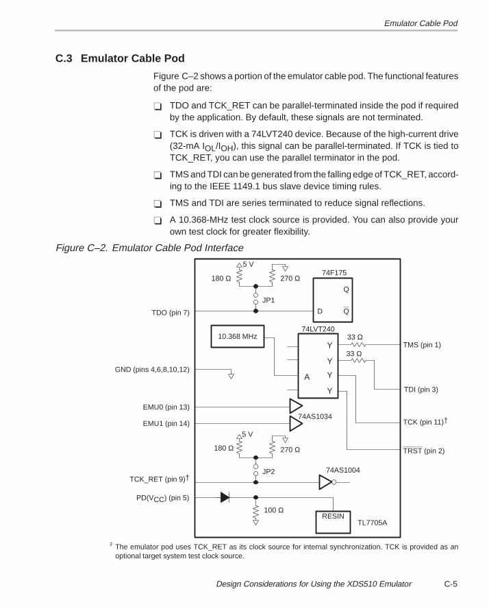
Emulator Cable Pod
C-5Design Considerations for Using the XDS510 Emulator
C.3 Emulator Cable Pod
Figure C–2 shows a portion of the emulator cable pod. The functional featuresof the pod are:
TDO and TCK_RET can be parallel-terminated inside the pod if requiredby the application. By default, these signals are not terminated.
TCK is driven with a 74LVT240 device. Because of the high-current drive(32-mA IOL/IOH), this signal can be parallel-terminated. If TCK is tied toTCK_RET, you can use the parallel terminator in the pod.
TMS and TDI can be generated from the falling edge of TCK_RET, accord-ing to the IEEE 1149.1 bus slave device timing rules.
TMS and TDI are series terminated to reduce signal reflections.
A 10.368-MHz test clock source is provided. You can also provide yourown test clock for greater flexibility.
Figure C–2. Emulator Cable Pod Interface
100 Ω
TL7705ARESIN
270 Ω
JP2
180 Ω
TCK_RET (pin 9)
EMU1 (pin 14)
EMU0 (pin 13)74AS1034
GND (pins 4,6,8,10,12)
TRST (pin 2)
TCK (pin 11)
10.368 MHz
33 Ω
33 Ω
TDI (pin 3)
TMS (pin 1)
TDO (pin 7)
74LVT240
180 Ω
JP1
270 Ω74F175
Q
Q
D
PD(VCC) (pin 5)
5 V
5 V
74AS1004
Y
Y
Y
Y
A
† The emulator pod uses TCK_RET as its clock source for internal synchronization. TCK is provided as anoptional target system test clock source.
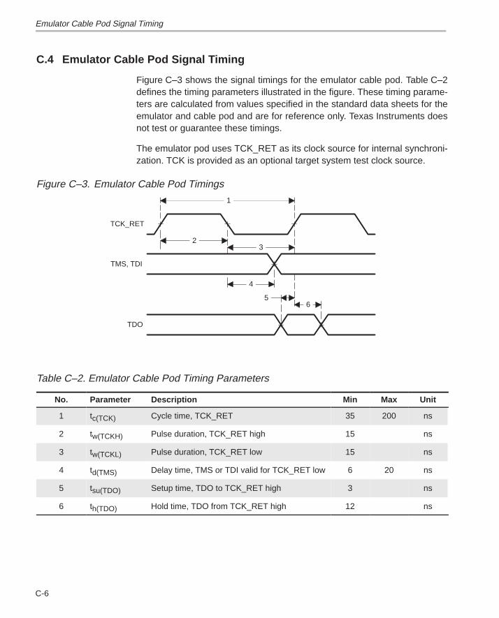
Emulator Cable Pod Signal Timing
C-6
C.4 Emulator Cable Pod Signal Timing
Figure C–3 shows the signal timings for the emulator cable pod. Table C–2defines the timing parameters illustrated in the figure. These timing parame-ters are calculated from values specified in the standard data sheets for theemulator and cable pod and are for reference only. Texas Instruments doesnot test or guarantee these timings.
The emulator pod uses TCK_RET as its clock source for internal synchroni-zation. TCK is provided as an optional target system test clock source.
Figure C–3. Emulator Cable Pod Timings
TDO
TMS, TDI
TCK_RET
65
4
32
1
Table C–2. Emulator Cable Pod Timing Parameters
No. Parameter Description Min Max Unit
1 tc(TCK) Cycle time, TCK_RET 35 200 ns
2 tw(TCKH) Pulse duration, TCK_RET high 15 ns
3 tw(TCKL) Pulse duration, TCK_RET low 15 ns
4 td(TMS) Delay time, TMS or TDI valid for TCK_RET low 6 20 ns
5 tsu(TDO) Setup time, TDO to TCK_RET high 3 ns
6 th(TDO) Hold time, TDO from TCK_RET high 12 ns
Emulation Timing Calculations
C-7Design Considerations for Using the XDS510 Emulator
C.5 Emulation Timing Calculations
The examples in this section help you calculate emulation timings in your sys-tem. For actual target timing parameters, see the appropriate data sheet forthe device you are emulating.
The examples use the following assumptions:
tsu(TTMS) Setup time, target TMS or TDI to TCKhigh 10 ns
td(TTDO) Delay time, target TDO from TCK low 15 ns
td(bufmax) Delay time, target buffer maximum 10 ns
td(bufmin) Delay time, target buffer minimum 1 ns
tbufskew Skew time, target buffer between two de-vices in the same package:[td(bufmax) – td(bufmin)] × 0.15
1.35 ns
tTCKfactor Duty cycle, assume a 40/60% duty cycleclock
0.4(40%)
Also, the examples use the following values from Table C–2 on page C-6:
td(TMSmax) Delay time, emulator TMS or TDI fromTCK_RET low, maximum
20 ns
tsu(TDOmin) Setup time, TDO to emulator TCK_REThigh, minimum
3 ns
There are two key timing paths to consider in the emulation design:
The TCK_RET-to-TMS or TDI path, called tpd(TCK_RET-TMS/TDI) (propaga-tion delay time)
The TCK_RET-to-TDO path, called tpd(TCK_RET-TDO)
In the examples, the worst-case path delay is calculated to determine themaximum system test clock frequency.
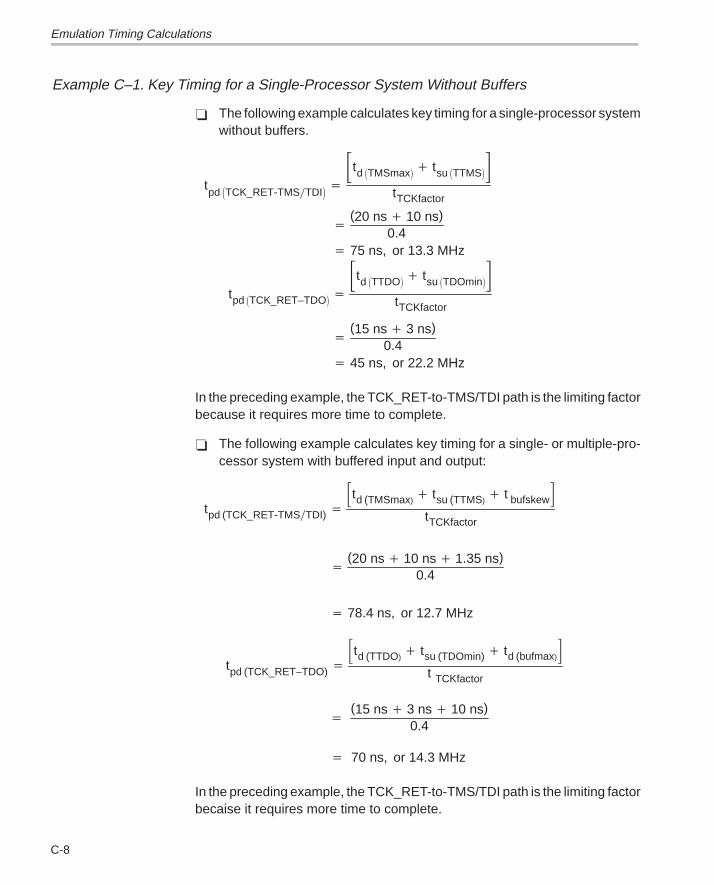
Emulation Timing Calculations
C-8
Example C–1. Key Timing for a Single-Processor System Without Buffers
The following example calculates key timing for a single-processor systemwithout buffers.
tpd TCK_RET-TMSTDI
td TMSmax tsu TTMStTCKfactor
(20 ns 10 ns)
0.4 75 ns, or 13.3 MHz
tpd TCK_RET–TDO td TTDO tsu TDOmin
tTCKfactor
(15 ns 3 ns)
0.4 45 ns, or 22.2 MHz
In the preceding example, the TCK_RET-to-TMS/TDI path is the limiting factorbecause it requires more time to complete.
The following example calculates key timing for a single- or multiple-pro-cessor system with buffered input and output:
tpd (TCK_RET-TMSTDI) td (TMSmax)
tsu (TTMS) t bufskew
tTCKfactor
(20 ns 10 ns 1.35 ns)
0.4
78.4 ns, or 12.7 MHz
tpd (TCK_RET–TDO) td (TTDO)
tsu (TDOmin) td (bufmax)
t TCKfactor
70 ns, or 14.3 MHz
(15 ns 3 ns 10 ns)
0.4
In the preceding example, the TCK_RET-to-TMS/TDI path is the limiting factorbecaise it requires more time to complete.
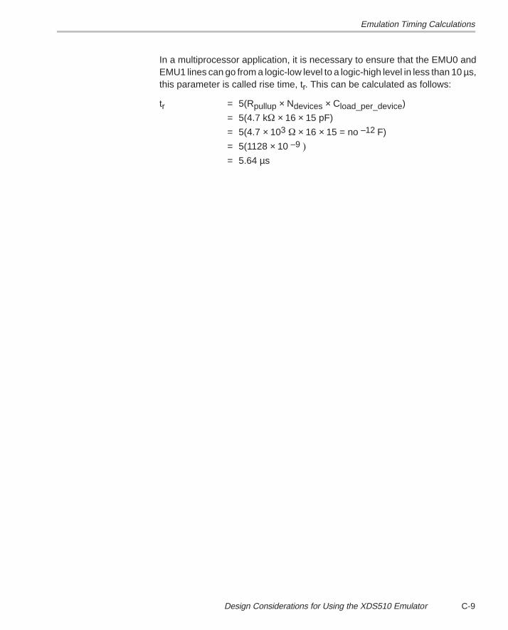
Emulation Timing Calculations
C-9Design Considerations for Using the XDS510 Emulator
In a multiprocessor application, it is necessary to ensure that the EMU0 andEMU1 lines can go from a logic-low level to a logic-high level in less than 10 µs,this parameter is called rise time, tr. This can be calculated as follows:
tr = 5(Rpullup × Ndevices × Cload_per_device)
= 5(4.7 k × 16 × 15 pF)
= 5(4.7 × 103 × 16 × 15 = no –12 F)
= 5(1128 × 10 –9
= 5.64 µs
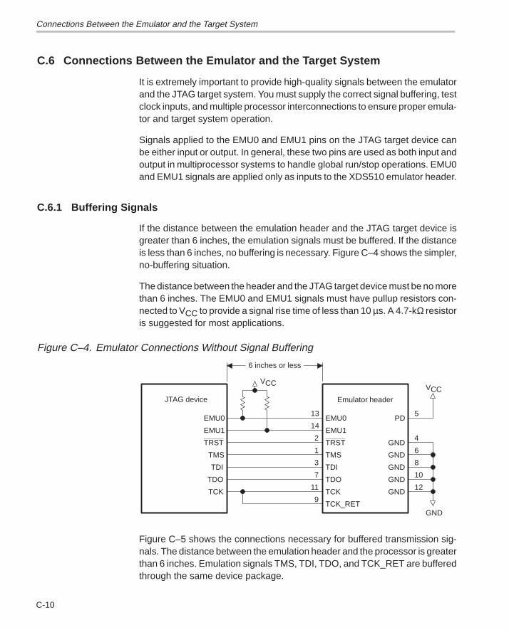
Connections Between the Emulator and the Target System
C-10
C.6 Connections Between the Emulator and the Target System
It is extremely important to provide high-quality signals between the emulatorand the JTAG target system. You must supply the correct signal buffering, testclock inputs, and multiple processor interconnections to ensure proper emula-tor and target system operation.
Signals applied to the EMU0 and EMU1 pins on the JTAG target device canbe either input or output. In general, these two pins are used as both input andoutput in multiprocessor systems to handle global run/stop operations. EMU0and EMU1 signals are applied only as inputs to the XDS510 emulator header.
C.6.1 Buffering Signals
If the distance between the emulation header and the JTAG target device isgreater than 6 inches, the emulation signals must be buffered. If the distanceis less than 6 inches, no buffering is necessary. Figure C–4 shows the simpler,no-buffering situation.
The distance between the header and the JTAG target device must be no morethan 6 inches. The EMU0 and EMU1 signals must have pullup resistors con-nected to VCC to provide a signal rise time of less than 10 µs. A 4.7-kΩ resistoris suggested for most applications.
Figure C–4. Emulator Connections Without Signal Buffering
VCC
Emulator header
VCC
GND
12
10
8
6
4
5
GND
GND
GND
GND
GND
PD
TCK_RET
TCK
TDO
TDI
TMS
TRST
EMU1
EMU0
9
11
7
3
1
2
14
13
JTAG device
TCK
TDO
TDI
TMS
TRST
EMU1
EMU0
6 inches or less
Figure C–5 shows the connections necessary for buffered transmission sig-nals. The distance between the emulation header and the processor is greaterthan 6 inches. Emulation signals TMS, TDI, TDO, and TCK_RET are bufferedthrough the same device package.
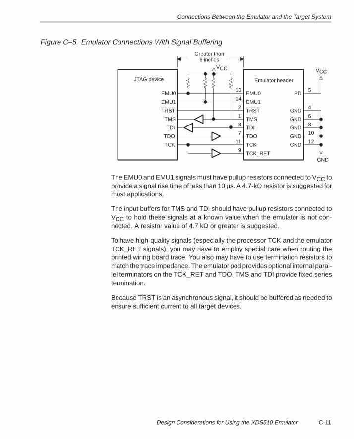
Connections Between the Emulator and the Target System
C-11Design Considerations for Using the XDS510 Emulator
Figure C–5. Emulator Connections With Signal Buffering
VCC
Emulator header
VCC
GND
12
10
8
6
4
5
GND
GND
GND
GND
GND
PD
TCK_RET
TCK
TDO
TDI
TMS
TRST
EMU1
EMU0
9
11
7
3
1
2
14
13
JTAG device
TCK
TDO
TDI
TMS
TRST
EMU1
EMU0
Greater than6 inches
The EMU0 and EMU1 signals must have pullup resistors connected to VCC toprovide a signal rise time of less than 10 µs. A 4.7-kΩ resistor is suggested formost applications.
The input buffers for TMS and TDI should have pullup resistors connected toVCC to hold these signals at a known value when the emulator is not con-nected. A resistor value of 4.7 kΩ or greater is suggested.
To have high-quality signals (especially the processor TCK and the emulatorTCK_RET signals), you may have to employ special care when routing theprinted wiring board trace. You also may have to use termination resistors tomatch the trace impedance. The emulator pod provides optional internal paral-lel terminators on the TCK_RET and TDO. TMS and TDI provide fixed seriestermination.
Because TRST is an asynchronous signal, it should be buffered as needed toensure sufficient current to all target devices.
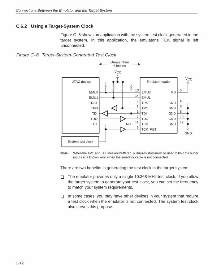
Connections Between the Emulator and the Target System
C-12
C.6.2 Using a Target-System Clock
Figure C–6 shows an application with the system test clock generated in thetarget system. In this application, the emulator’s TCK signal is leftunconnected.
Figure C–6. Target-System-Generated Test Clock
NC
System test clock
VCC
Emulator header
GND
12
10
8
6
4
5
GND
GND
GND
GND
GND
PD
TCK_RET
TCK
TDO
TDI
TMS
TRST
EMU1
EMU0
9
11
7
3
1
2
14
13
JTAG device
TCK
TDO
TDI
TMS
TRST
EMU1
EMU0
Greater than6 inches
VCC
Note: When the TMS and TDI lines are buffered, pullup resistors must be used to hold the bufferinputs at a known level when the emulator cable is not connected.
There are two benefits in generating the test clock in the target system:
The emulator provides only a single 10.368-MHz test clock. If you allowthe target system to generate your test clock, you can set the frequencyto match your system requirements.
In some cases, you may have other devices in your system that requirea test clock when the emulator is not connected. The system test clockalso serves this purpose.
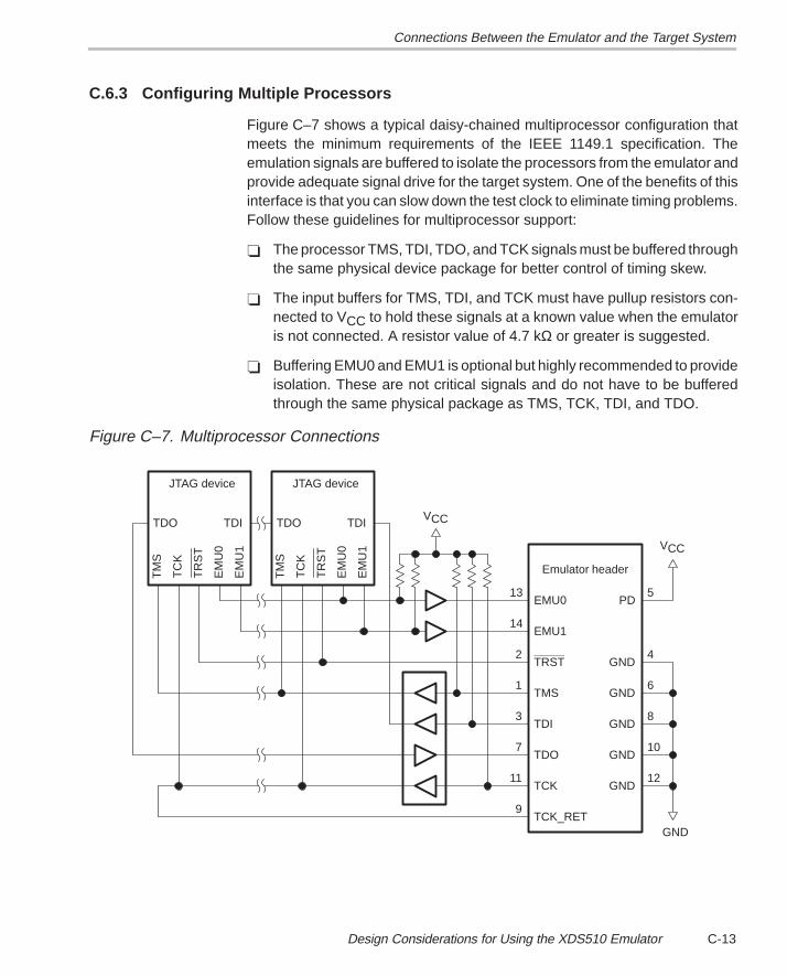
Connections Between the Emulator and the Target System
C-13Design Considerations for Using the XDS510 Emulator
C.6.3 Configuring Multiple Processors
Figure C–7 shows a typical daisy-chained multiprocessor configuration thatmeets the minimum requirements of the IEEE 1149.1 specification. Theemulation signals are buffered to isolate the processors from the emulator andprovide adequate signal drive for the target system. One of the benefits of thisinterface is that you can slow down the test clock to eliminate timing problems.Follow these guidelines for multiprocessor support:
The processor TMS, TDI, TDO, and TCK signals must be buffered throughthe same physical device package for better control of timing skew.
The input buffers for TMS, TDI, and TCK must have pullup resistors con-nected to VCC to hold these signals at a known value when the emulatoris not connected. A resistor value of 4.7 kΩ or greater is suggested.
Buffering EMU0 and EMU1 is optional but highly recommended to provideisolation. These are not critical signals and do not have to be bufferedthrough the same physical package as TMS, TCK, TDI, and TDO.
Figure C–7. Multiprocessor Connections
TDITDI TDOTDO
JTAG deviceJTAG device
VCC
Emulator header
GND
12
10
8
6
4
5
GND
GND
GND
GND
GND
PD
TCK_RET
TCK
TDO
TDI
TMS
TRST
EMU1
EMU0
9
11
7
3
1
2
14
13
TM
S
TC
K
TR
ST
EM
U0
EM
U1
TM
S
TC
K
TR
ST
EM
U0
EM
U1 VCC
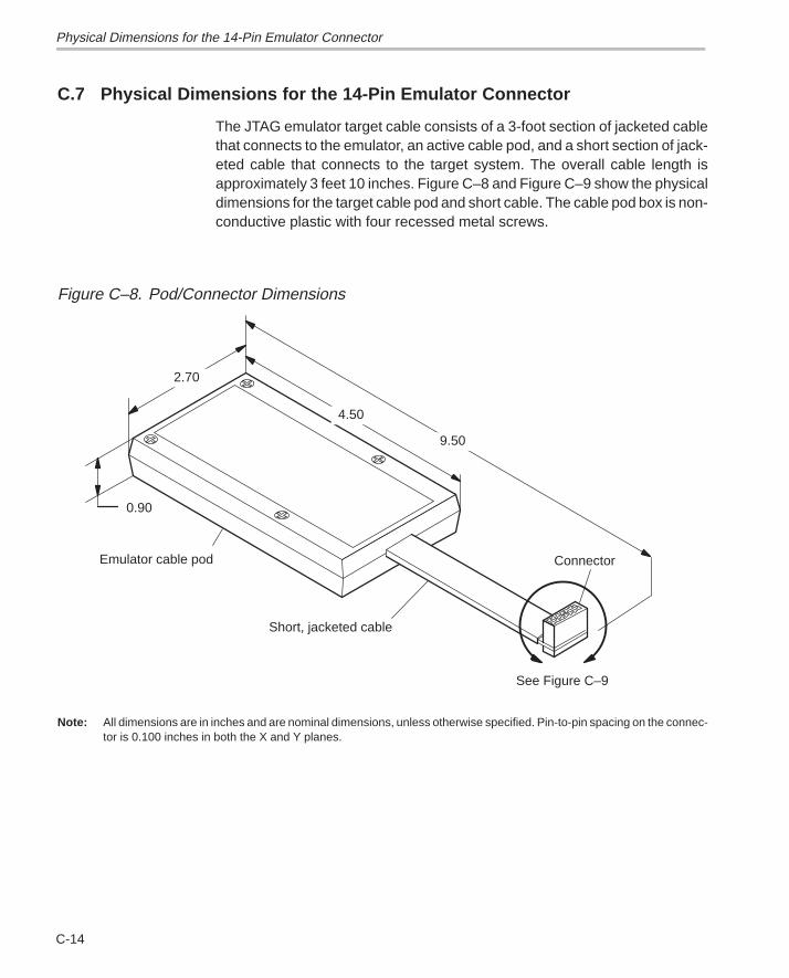
Physical Dimensions for the 14-Pin Emulator Connector
C-14
C.7 Physical Dimensions for the 14-Pin Emulator Connector
The JTAG emulator target cable consists of a 3-foot section of jacketed cablethat connects to the emulator, an active cable pod, and a short section of jack-eted cable that connects to the target system. The overall cable length isapproximately 3 feet 10 inches. Figure C–8 and Figure C–9 show the physicaldimensions for the target cable pod and short cable. The cable pod box is non-conductive plastic with four recessed metal screws.
Figure C–8. Pod/Connector Dimensions
0.90
2.70
4.50
9.50
See Figure C–9
Emulator cable pod
Short, jacketed cable
Connector
Note: All dimensions are in inches and are nominal dimensions, unless otherwise specified. Pin-to-pin spacing on the connec-tor is 0.100 inches in both the X and Y planes.
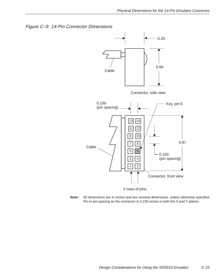
Physical Dimensions for the 14-Pin Emulator Connector
C-15Design Considerations for Using the XDS510 Emulator
Figure C–9. 14-Pin Connector Dimensions
0.100(pin spacing)
Key, pin 6
0.100(pin spacing)
0.87
0.66
0.20
Cable
Connector, side view
Connector, front view
Cable
1
3
5
7
9
11
13
2
4
6
8
10
12
14
2 rows of pins
Note: All dimensions are in inches and are nominal dimensions, unless otherwise specified.Pin-to-pin spacing on the connector is 0.100 inches in both the X and Y planes.
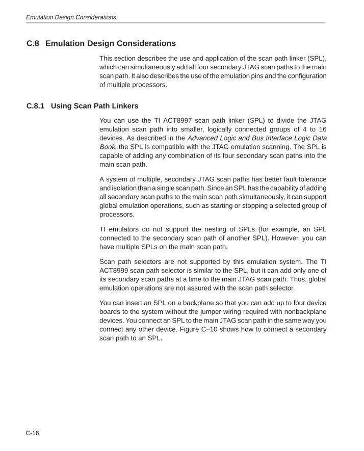
Emulation Design Considerations
C-16
C.8 Emulation Design Considerations
This section describes the use and application of the scan path linker (SPL),which can simultaneously add all four secondary JTAG scan paths to the mainscan path. It also describes the use of the emulation pins and the configurationof multiple processors.
C.8.1 Using Scan Path Linkers
You can use the TI ACT8997 scan path linker (SPL) to divide the JTAGemulation scan path into smaller, logically connected groups of 4 to 16devices. As described in the Advanced Logic and Bus Interface Logic DataBook, the SPL is compatible with the JTAG emulation scanning. The SPL iscapable of adding any combination of its four secondary scan paths into themain scan path.
A system of multiple, secondary JTAG scan paths has better fault toleranceand isolation than a single scan path. Since an SPL has the capability of addingall secondary scan paths to the main scan path simultaneously, it can supportglobal emulation operations, such as starting or stopping a selected group ofprocessors.
TI emulators do not support the nesting of SPLs (for example, an SPLconnected to the secondary scan path of another SPL). However, you canhave multiple SPLs on the main scan path.
Scan path selectors are not supported by this emulation system. The TIACT8999 scan path selector is similar to the SPL, but it can add only one ofits secondary scan paths at a time to the main JTAG scan path. Thus, globalemulation operations are not assured with the scan path selector.
You can insert an SPL on a backplane so that you can add up to four deviceboards to the system without the jumper wiring required with nonbackplanedevices. You connect an SPL to the main JTAG scan path in the same way youconnect any other device. Figure C–10 shows how to connect a secondaryscan path to an SPL.
Emulation Design Considerations
C-17Design Considerations for Using the XDS510 Emulator
Figure C–10. Connecting a Secondary JTAG Scan Path to a Scan Path Linker
TDI
TCK
TDO
TRST
TMS
TDO
TRST
TCK
TMS
TDI
DTDI0
DTMS0
DTDO0
DTCK
TDO
TRST
TCK
TMS
TDI
SPL
JTAG 0
JTAG nDTDI1
DTMS1
DTDO1
DTDI2
DTMS2
DTDO2
DTDI3
DTMS3
DTDO3
. . .
The TRST signal from the main scan path drives all devices, even those onthe secondary scan paths of the SPL. The TCK signal on each target deviceon the secondary scan path of an SPL is driven by the SPL’s DTCK signal. TheTMS signal on each device on the secondary scan path is driven by the respec-tive DTMS signals on the SPL.
DTDO0 on the SPL is connected to the TDI signal of the first device on the sec-ondary scan path. DTDI0 on the SPL is connected to the TDO signal of the lastdevice in the secondary scan path. Within each secondary scan path, the TDIsignal of a device is connected to the TDO signal of the device before it. If theSPL is on a backplane, its secondary JTAG scan paths are on add-on boards;if signal degradation is a problem, you may need to buffer both the TRST andDTCK signals. Although degradation is less likely for DTMSn signals, you mayalso need to buffer them for the same reasons.
Emulation Design Considerations
C-18
C.8.2 Emulation Timing Calculations for a Scan Path Linker (SPL)
The examples in this section help you to calculate the key emulation timingsin the SPL secondary scan path of your system. For actual target timing pa-rameters, see the appropriate device data sheet for your target device.
The examples use the following assumptions:
tsu(TTMS) Setup time, target TMS/TDI to TCK high 10 ns
td(TTDO) Delay time, target TDO from TCK low 15 ns
td(bufmax) Delay time, target buffer, maximum 10 ns
td(bufmin) Delay time, target buffer, minimum 1 ns
t(bufskew) Skew time, target buffer, between twodevices in the same package:[td(bufmax) – td(bufmin)] × 0.15
1.35 ns
t(TCKfactor) Duty cycle, TCK assume a 40/60% clock 0.4(40%)
Also, the examples use the following values from the SPL data sheet:
td(DTMSmax) Delay time, SPL DTMS/DTDO from TCKlow, maximum
31 ns
tsu(DTDLmin) Setup time, DTDI to SPL TCK high,minimum
7 ns
td(DTCKHmin) Delay time, SPL DTCK from TCK high,minimum
2 ns
td(DTCKLmax) Delay time, SPL DTCK from TCK low,maximum
16 ns
There are two key timing paths to consider in the emulation design:
The TCK-to-DTMS/DTDO path, called tpd(TCK-DTMS) The TCK-to-DTDI path, called tpd(TCK-DTDI)
Emulation Design Considerations
C-19Design Considerations for Using the XDS510 Emulator
In the following two examples, the worst-case path delay is calculated to deter-mine the maximum system test clock frequency.
Example C–2. Key Timing for a Single-Processor System Without Buffering (SPL)
The following example calculates key timing for a single-processor systemwithout buffering (SPL):
tpd TCK-DTMS td DTMSmax td DTCKHmin tsu TTMS
tTCKfactor
(31 ns 2 ns 10 ns)
0.4
107.5 ns, or 9.3 MHz
tpd TCK-DTDI
td TTDO t
d DTCKLmax tsu DTDLmin
tTCKfactor
(15 ns 16 ns 7 ns)
0.4
9.5 ns, or 10.5 MHz
In the preceding example, the TCK-to-DTMS/DTDL path is the limiting factor.
The following example calculates key timing for a single- or multiprocessor-system with buffered input and output (SPL):
tpd (TCK-TDMS) td (DTMSmax) tDTCKHmin tsu (TTMS) t(bufskew)
tTCKfactor
(31 ns 2 ns 10 ns 1.35 ns)
0.4
110.9 ns, or 9.0 MHz
tpd (TCK–DTDI) td (TTDO) td DTCKLmax tsu (DTDLmin)
td (bufskew)tTCKfactor
120 ns, or 8.3 MHz
(15 ns 15 ns 7 ns 10 ns)
0.4
In the preceding example, the TCK-to-DTDI path is the limiting factor.
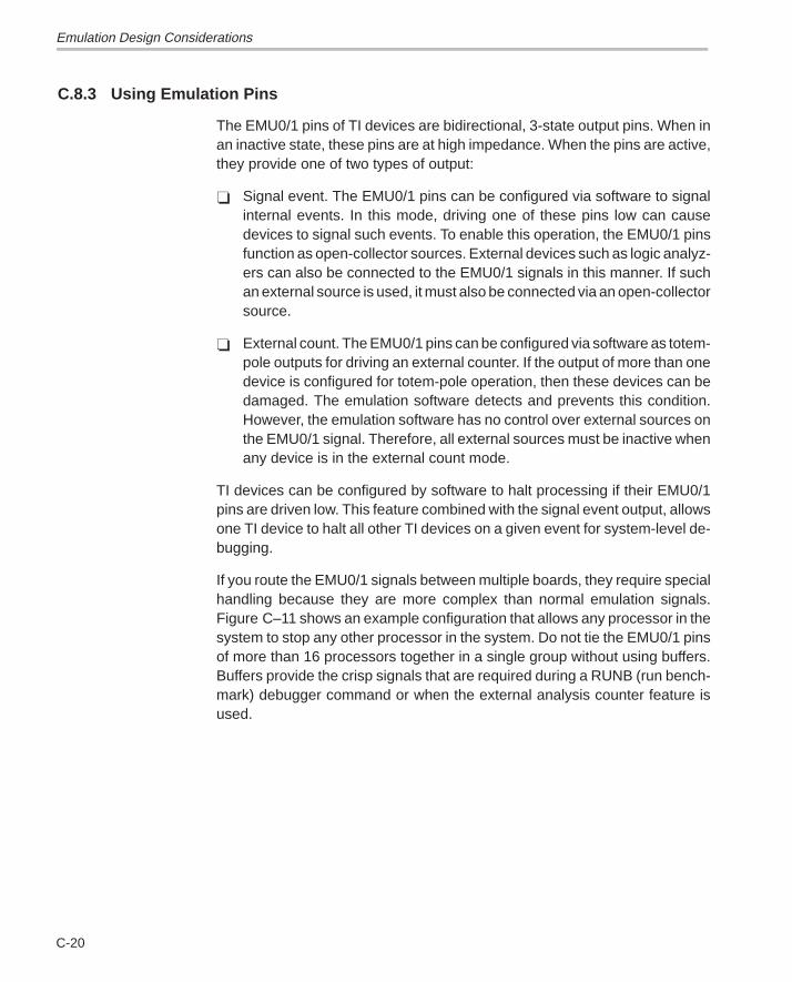
Emulation Design Considerations
C-20
C.8.3 Using Emulation Pins
The EMU0/1 pins of TI devices are bidirectional, 3-state output pins. When inan inactive state, these pins are at high impedance. When the pins are active,they provide one of two types of output:
Signal event. The EMU0/1 pins can be configured via software to signalinternal events. In this mode, driving one of these pins low can causedevices to signal such events. To enable this operation, the EMU0/1 pinsfunction as open-collector sources. External devices such as logic analyz-ers can also be connected to the EMU0/1 signals in this manner. If suchan external source is used, it must also be connected via an open-collectorsource.
External count. The EMU0/1 pins can be configured via software as totem-pole outputs for driving an external counter. If the output of more than onedevice is configured for totem-pole operation, then these devices can bedamaged. The emulation software detects and prevents this condition.However, the emulation software has no control over external sources onthe EMU0/1 signal. Therefore, all external sources must be inactive whenany device is in the external count mode.
TI devices can be configured by software to halt processing if their EMU0/1pins are driven low. This feature combined with the signal event output, allowsone TI device to halt all other TI devices on a given event for system-level de-bugging.
If you route the EMU0/1 signals between multiple boards, they require specialhandling because they are more complex than normal emulation signals.Figure C–11 shows an example configuration that allows any processor in thesystem to stop any other processor in the system. Do not tie the EMU0/1 pinsof more than 16 processors together in a single group without using buffers.Buffers provide the crisp signals that are required during a RUNB (run bench-mark) debugger command or when the external analysis counter feature isused.
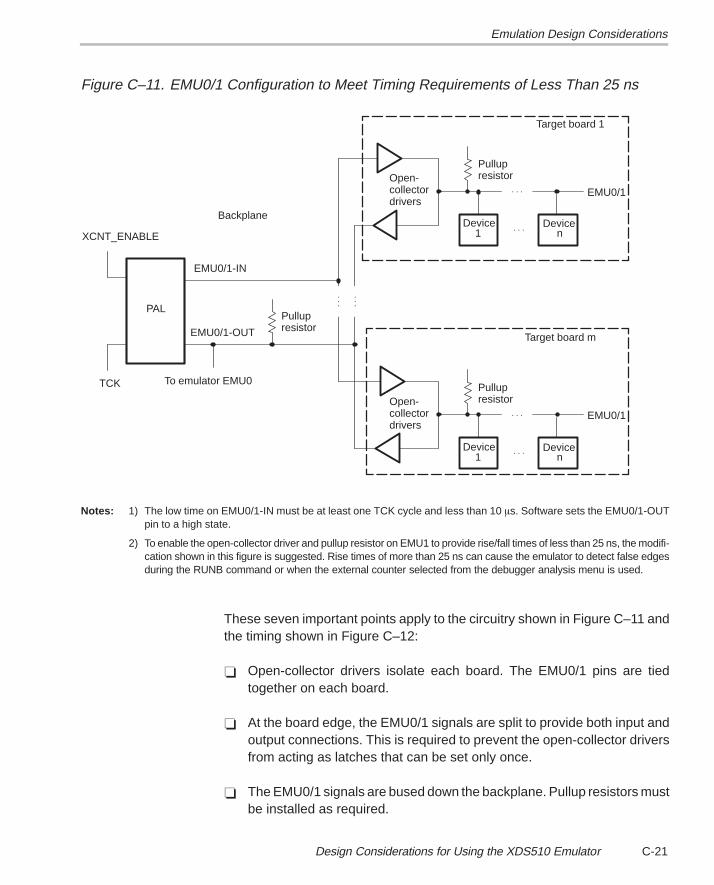
Emulation Design Considerations
C-21Design Considerations for Using the XDS510 Emulator
Figure C–11. EMU0/1 Configuration to Meet Timing Requirements of Less Than 25 ns
Open-collectordrivers
EMU0/1-IN
Backplane
Target board m
TCK
XCNT_ENABLE
To emulator EMU0
PALPullupresistor
Open-collectordrivers
Target board 1
EMU0/1
EMU0/1-OUT
. . .Device Device
EMU0/1
. . .
. . .
. . .
. . .
. . .
1 n
Device Device1 n
Pullupresistor
Pullupresistor
Notes: 1) The low time on EMU0/1-IN must be at least one TCK cycle and less than 10 s. Software sets the EMU0/1-OUTpin to a high state.
2) To enable the open-collector driver and pullup resistor on EMU1 to provide rise/fall times of less than 25 ns, the modifi-cation shown in this figure is suggested. Rise times of more than 25 ns can cause the emulator to detect false edgesduring the RUNB command or when the external counter selected from the debugger analysis menu is used.
These seven important points apply to the circuitry shown in Figure C–11 andthe timing shown in Figure C–12:
Open-collector drivers isolate each board. The EMU0/1 pins are tiedtogether on each board.
At the board edge, the EMU0/1 signals are split to provide both input andoutput connections. This is required to prevent the open-collector driversfrom acting as latches that can be set only once.
The EMU0/1 signals are bused down the backplane. Pullup resistors mustbe installed as required.
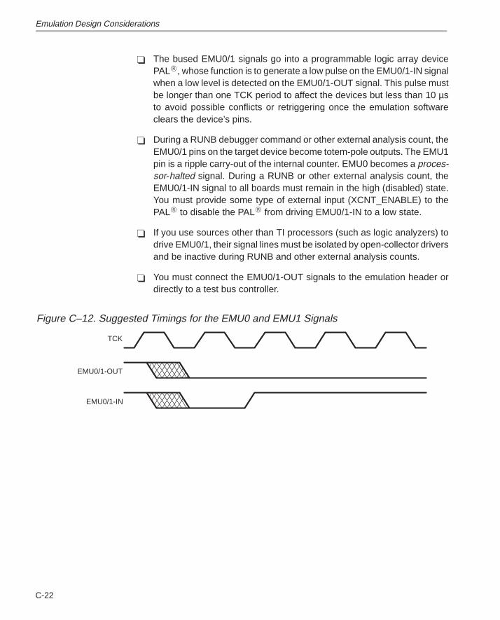
Emulation Design Considerations
C-22
The bused EMU0/1 signals go into a programmable logic array devicePAL, whose function is to generate a low pulse on the EMU0/1-IN signalwhen a low level is detected on the EMU0/1-OUT signal. This pulse mustbe longer than one TCK period to affect the devices but less than 10 µsto avoid possible conflicts or retriggering once the emulation softwareclears the device’s pins.
During a RUNB debugger command or other external analysis count, theEMU0/1 pins on the target device become totem-pole outputs. The EMU1pin is a ripple carry-out of the internal counter. EMU0 becomes a proces-sor-halted signal. During a RUNB or other external analysis count, theEMU0/1-IN signal to all boards must remain in the high (disabled) state.You must provide some type of external input (XCNT_ENABLE) to thePAL to disable the PAL from driving EMU0/1-IN to a low state.
If you use sources other than TI processors (such as logic analyzers) todrive EMU0/1, their signal lines must be isolated by open-collector driversand be inactive during RUNB and other external analysis counts.
You must connect the EMU0/1-OUT signals to the emulation header ordirectly to a test bus controller.
Figure C–12. Suggested Timings for the EMU0 and EMU1 Signals
EMU0/1-IN
EMU0/1-OUT
TCK
Emulation Design Considerations
C-23Design Considerations for Using the XDS510 Emulator
Figure C–13. EMU0/1 Configuration With Additional AND Gate to Meet TimingRequirements of Greater Than 25 ns
Open-collectordrivers
EMU0/1-IN
Backplane
Target board m
TCK
XCNT_ENABLE
To emulator EMU0
PALPullupresistor
Open-collectordrivers
Target board 1
EMU0/1
EMU1 signal from other boards
EMU1AND
To emulator EMU1
Circuitry required for >25-ns rise/fall time modification
EMU0/1-OUT
. . .Device Device
EMU0/1
. . .
. . .
. . .
. . .
. . .
. . .
1 n
Device Device1 n
Up tom boards
Pullupresistor
Pullupresistor
Notes: 1) The low time on EMU0/1-IN must be at least one TCK cycle and less than 10 s. Software sets the EMU0/1-OUT pinto a high state.
2) To enable the open-collector driver and pullup resistor on EMU1 to provide rise/fall time of greater than 25 ns, themodification shown in this figure is suggested. Rise times of more than 25 ns can cause the emulator to detect falseedges during the RUNB command or when the external counter selected from the debugger analysis menu is used.
Emulation Design Considerations
C-24
You do not need to have devices on one target board stop devices on anothertarget board using the EMU0/1 signals (see the circuit in Figure C–14). In thisconfiguration, the global-stop capability is lost. It is important not to overloadEMU0/1 with more than 16 devices.
Figure C–14. EMU0/1 Configuration Without Global Stop
EMU0/1
To emulator
. . .
EMU0/1
. . .Device Device
EMU0/1
. . .
. . .
. . .
1 n
Device Device1 n
. . .
Target board m
Target board 1
Pullupresistor
Pullupresistor
Pullupresistor
Note: The open-collector driver and pullup resistor on EMU1 must be able to provide rise/fall times of less than 25 ns. Rise timesof more than 25 ns can cause the emulator to detect false edges during the RUNB command or when the external counterselected from the debugger analysis menu is used. If this condition cannot be met, then the EMU0/1 signals from theindividual boards must be ANDed together (as shown in Figure C–14) to produce an EMU0/1 signal for the emulator.
C.8.4 Performing Diagnostic Applications
For systems that require built-in diagnostics, it is possible to connect theemulation scan path directly to a TI ACT8990 test bus controller (TBC) insteadof the emulation header. The TBC is described in the Texas InstrumentsAdvanced Logic and Bus Interface Logic Data Book. Figure C–15 shows thescan path connections of n devices to the TBC.
Emulation Design Considerations
C-25Design Considerations for Using the XDS510 Emulator
Figure C–15. TBC Emulation Connections for n JTAG Scan Paths
JTAG 0
JTAG nTDI
EMU1
TMS
TDO
EMU0
TRST
TCK
TDO
TCK
TRST
EMU1
EMU0
TMS
TDI
Clock
TDI1
TDI0
TCKO
TMS5/EVNT3
TMS4/EVNT2
TMS3/EVNT1
TMS2/EVNT0
TMS1
TMS0
TDO
TCKI
VCC
TBC
In the system design shown in Figure C–15, the TBC emulation signals TCKI,TDO, TMS0, TMS2/EVNT0, TMS3/EVNT1, TMS5/EVNT3, TCKO, and TDI0are used, and TMS1, TMS4/EVNT2, and TDI1 are not connected. The targetdevices’ EMU0 and EMU1 signals are connected to VCC through pullup resis-tors and tied to the TBC’s TMS2/EVNT0 and TMS3/EVNT1 pins, respectively.The TBC’s TCKI pin is connected to a clock generator. The TCK signal for themain JTAG scan path is driven by the TBC’s TCKO pin.
On the TBC, the TMS0 pin drives the TMS pins on each device on the mainJTAG scan path. TDO on the TBC connects to TDI on the first device on themain JTAG scan path. TDI0 on the TBC is connected to the TDO signal of thelast device on the main JTAG scan path. Within the main JTAG scan path, theTDI signal of a device is connected to the TDO signal of the device before it.TRST for the devices can be generated either by inverting the TBC’sTMS5/EVNT3 signal for software control or by logic on the board itself.
D-1
Appendix A
Glossary
AA0–A15: Collectively, the external address bus; the 16 pins are used in par-
allel to address external data memory, program memory, or I/O space.
ACC: See accumulator.
ACCH: Accumulator high word. The upper 16 bits of the accumulator. Seealso accumulator.
ACCL: Accumulator low word. The lower 16 bits of the accumulator. Seealso accumulator.
accumulator: A 32-bit register that stores the results of operations in thecentral arithmetic logic unit (CALU) and provides an input for subsequentCALU operations. The accumulator also performs shift and rotate opera-tions.
address: The location of program code or data stored in memory.
addressing mode: A method by which an instruction interprets its operandsto acquire the data it needs. See also direct addressing; immediateaddressing; indirect addressing.
analog-to-digital (A/D) converter: A circuit that translates an analog signalto a digital signal.
AR: See auxiliary register.
AR0–AR7: Auxiliary registers 0 through 7. See auxiliary register.
ARAU: See auxiliary register arithmetic unit (ARAU).
ARB: See auxiliary register pointer buffer (ARB).
ARP: See auxiliary register pointer (ARP).
auxiliary register: One of eight 16-bit registers (AR7–AR0) used as point-ers to addresses in data space. The registers are operated on by the aux-iliary register arithmetic unit (ARAU) and are selected by the auxiliaryregister pointer (ARP).
Appendix D
Glossary
D-2
auxiliary register arithmetic unit (ARAU): A 16-bit arithmetic unit used toincrement, decrement, or compare the contents of the auxiliary registers.Its primary function is manipulating auxiliary register values for indirectaddressing.
auxiliary register pointer (ARP): A 3-bit field in status register ST0 thatpoints to the current auxiliary register.
auxiliary register pointer buffer (ARB): A 3-bit field in status register ST1that holds the previous value of the auxiliary register pointer (ARP).
B
B0: An on-chip block of dual-access RAM that can be configured as eitherdata memory or program memory, depending on the value of the CNFbit in status register ST1.
B1: An on-chip block of dual-access RAM available for data memory.
B2: An on-chip block of dual-access RAM available for data memory.
BIO pin : A general-purpose input pin that can be tested by conditionalinstructions that cause a branch when an external device drives BIO low.
bit-reversed indexed addressing : A method of indirect addressing thatallows efficient I/O operations by resequencing the data points in aradix-2 fast Fourier transform (FFT) program. The direction of carrypropagation in the ARAU is reversed.
boot loader: A built-in segment of code that transfers code from an externalsource to a 16-bit external program destination at reset.
BR: Bus request pin. This pin is tied to the BR signal, which is asserted whena global data memory access is initiated.
branch: A switching of program control to a nonsequential program-memory address.
Glossary
D-3Glossary
C
C bit: See carry bit.
CALU: See central arithmetic logic unit (CALU).
carry bit: Bit 9 of status register ST1; used by the CALU for extendedarithmetic operations and accumulator shifts and rotates. The carry bitcan be tested by conditional instructions.
central arithmetic logic unit (CALU): The 32-bit wide main arithmetic logicunit for the ’C24x CPU that performs arithmetic and logic operations. Itaccepts 32-bit values for operations, and its 32-bit output is held in theaccumulator.
CLKIN: Input clock signal. A clock source signal supplied to the on-chipclock generator at the CLKIN/X2 pin or generated internally by theon-chip oscillator. The clock generator divides or multiplies CLKIN toproduce the CPU clock signal, CLKOUT1.
CLKOUT: Master clock output signal. The output signal of the on-chip clockgenerator. The CLKOUT1 high pulse signifies the CPU’s logic phase(when internal values are changed), and the CLKOUT1 low pulsesignifies the CPU’s latch phase (when the values are held constant).
clock mode (clock generator): One of the modes which sets the internalCPU clock frequency to a fraction or multiple of the frequency of the inputclock signal CLKIN.
CNF bit: DARAM configuration bit. Bit 12 in status register ST1. CNF is usedto determine whether the on-chip RAM block B0 is mapped to programspace or data space.
codec: A device that codes in one direction of transmission and decodes inanother direction of transmission.
COFF: Common object file format. A system of files configured according toa standard developed by AT&T. These files are relocatable in memoryspace.
context saving/restoring : Saving the system status when the deviceenters a subroutine (such as an interrupt service routine) and restoringthe system status when exiting the subroutine. On the ’C24x, only theprogram counter value is saved and restored automatically; othercontext saving and restoring must be performed by the subroutine.
Glossary
D-4
CPU: Central processing unit. The ’C24x CPU is the portion of the processorinvolved in arithmetic, shifting, and Boolean logic operations, as well asthe generation of data- and program-memory addresses. The CPUincludes the central arithmetic logic unit (CALU), the multiplier, and theauxiliary register arithmetic unit (ARAU).
CPU cycle: The time required for the CPU to go through one logic phase(during which internal values are changed) and one latch phase (duringwhich the values are held constant).
current AR: See current auxiliary register.
current auxiliary register: The auxiliary register pointed to by the auxiliaryregister pointer (ARP). The auxiliary registers are AR0 (ARP = 0)through AR7 (ARP = 7). See also auxiliary register; next auxiliaryregister.
current data page: The data page indicated by the content of the data pagepointer (DP). See also data page; DP.
D
D0–D15: Collectively, the external data bus; the 16 pins are used in parallelto transfer data between the ’C24x and external data memory, programmemory, or I/O space.
DARAM: Dual-access RAM. RAM that can be accessed twice in a singleCPU clock cycle. For example, your code can read from and write toDARAM in the same clock cycle.
DARAM configuration bit (CNF): See CNF bit.
data-address generation logic: Logic circuitry that generates the address-es for data memory reads and writes. This circuitry, which includes theauxiliary registers and the ARAU, can generate one address permachine cycle. See also program-address generation logic.
data page: One block of 128 words in data memory. Data memory contains512 data pages. Data page 0 is the first page of data memory (addresses0000h–007Fh); data page 511 is the last page (addressesFF80h–FFFFh). See also data page pointer (DP); direct addressing.
data page 0: Addresses 0000h–007Fh in data memory; contains thememory-mapped registers, a reserved test/emulation area for specialinformation transfers, and the scratch-pad RAM block (B2).
Glossary
D-5Glossary
data page pointer (DP): A 9-bit field in status register ST0 that specifieswhich of the 512 data pages is currently selected for direct addressgeneration. When an instruction uses direct addressing to access a data-memory value, the DP provides the nine MSBs of the data-memoryaddress, and the instruction provides the seven LSBs.
data-read address bus (DRAB): A 16-bit internal bus that carries theaddress for each read from data memory.
data read bus (DRDB): A 16-bit internal bus that carries data from datamemory to the CALU and the ARAU.
data-write address bus (DWAB): A 16-bit internal bus that carries theaddress for each write to data memory.
data write bus (DWEB): A 16-bit internal bus that carries data to bothprogram memory and data memory.
decode phase: The phase of the pipeline in which the instruction isdecoded. See also pipeline; instruction-fetch phase; operand-fetchphase; instruction-execute phase.
direct addressing: One of the methods used by an instruction to addressdata-memory. In direct addressing, the data-page pointer (DP) holds thenine MSBs of the address (the current data page), and the instructionword provides the seven LSBs of the address (the offset). See alsoindirect addressing.
DP: See data page pointer (DP).
DRAB: See data-read address bus (DRAB).
DRDB: See data read bus (DRDB).
DS: Data memory select pin. The ’C24x asserts DS to indicate an access toexternal data memory (local or global).
DSWS: Data-space wait-state bit(s). A value in the wait-state generatorcontrol register (WSGR) that determines the number of wait statesapplied to reads from and writes to off-chip data space.
dual-access RAM : See DARAM.
dummy cycle: A CPU cycle in which the CPU intentionally reloads theprogram counter with the same address.
DWAB: See data-write address bus (DWAB).
DWEB: See data write bus (DWEB).
Glossary
D-6
E
execute phase: The fourth phase of the pipeline; the phase in which theinstruction is executed. See also pipeline; instruction-fetch phase;instruction-decode phase; operand-fetch phase.
external interrupt: A hardware interrupt triggered by an external eventsending an input through an interrupt pin.
F
FIFO buffer: First-in, first-out buffer. A portion of memory in which data isstored and then retrieved in the same order in which it was stored. Thesynchronous serial port has two four-word-deep FIFO buffers: one for itstransmit operation and one for its receive operation.
flash memory: Electronically erasable and programmable, nonvolatile(read-only) memory.
G
general-purpose input/output pins: Pins that can be used to accept inputsignals or send output signals. These pins are the input pin BIO, the out-put pin XF, and the GPIO pins.
global data space : One of the four ’C24x address spaces. The global dataspace can be used to share data with other processors within a systemand can serve as additional data space. See also local data space.
GREG: Global memory allocation register. A memory-mapped registerused for specifying the size of the global data memory. Addresses notallocated by the GREG for global data memory are available for localdata memory.
H
hardware interrupt: An interrupt triggered through physical connectionswith on-chip peripherals or external devices.
Glossary
D-7Glossary
Iimmediate addressing: One of the methods for obtaining data values used
by an instruction; the data value is a constant embedded directly into theinstruction word; data memory is not accessed.
immediate operand/immediate value: A constant given as an operand inan instruction that is using immediate addressing.
IMR: See interrupt mask register (IMR).
indirect addressing: One of the methods for obtaining data values used byan instruction. When an instruction uses indirect addressing, datamemory is addressed by the current auxiliary register. See also directaddressing.
input clock signal: See CLKIN.
input shifter: A 16- to 32-bit left barrel shifter that shifts incoming 16-bit datafrom 0 to 16 positions left relative to the 32-bit output.
instruction-decode phase: The second phase of the pipeline; the phase inwhich the instruction is decoded. See also pipeline; instruction-fetchphase; operand-fetch phase; instruction-execute phase.
instruction-execute phase: The fourth phase of the pipeline; the phase inwhich the instruction is executed. See also pipeline; instruction-fetchphase; instruction-decode phase; operand-fetch phase.
instruction-fetch phase: The first phase of the pipeline; the phase in whichthe instruction is fetched from program-memory. See also pipeline;instruction-decode phase; operand-fetch phase; instruction-executephase.
instruction register (IR): A 16-bit register that contains the instructionbeing executed.
instruction word: A 16-bit value representing all or half of an instruction. Aninstruction that is fully represented by 16 bits uses one instruction word.An instruction that must be represented by 32 bits uses two instructionwords (the second word is a constant).
internal interrupt: A hardware interrupt caused by an on-chip peripheral.
interrupt: A signal sent to the CPU that (when not masked or disabled)forces the CPU into a subroutine called an interrupt service routine (ISR).This signal can be triggered by an external device, an on-chip peripheral,or an instruction (INTR, NMI, or TRAP).
Glossary
D-8
interrupt acknowledge signal (IACK ): A signal that indicates an interrupthas been received and that the program counter is fetching the interruptvector that will force the processor into the appropriate interrupt serviceroutine.
interrupt flag register (IFR): A 16-bit memory-mapped register that indi-cates pending interrupts. Read the IFR to identify pending interrupts andwrite to the IFR to clear selected interrupts. Writing a 1 to any IFR flagbit clears that bit to 0.
interrupt latency: The delay between the time an interrupt request is madeand the time it is serviced.
interrupt mask register (IMR): A 16-bit memory-mapped register used tomask external and internal interrupts. Writing a 1 to any IMR bit positionenables the corresponding interrupt (when INTM = 0).
interrupt mode bit (INTM): Bit 9 in status register ST0; either enables allmaskable interrupts that are not masked by the IMR or disables all mask-able interrupts.
interrupt service routine (ISR) : A module of code that is executed inresponse to a hardware or software interrupt.
interrupt trap: See interrupt service routine (ISR).
interrupt vector: A branch instruction that leads the CPU to an interruptservice routine (ISR).
interrupt vector location: An address in program memory where an inter-rupt vector resides. When an interrupt is acknowledged, the CPUbranches to the interrupt vector location and fetches the interrupt vector.
INTM bit: See interrupt mode bit (INTM).
I/O-mapped register: One of the on-chip registers mapped to addresses inI/O (input/output) space. These registers, which include the registers forthe on-chip peripherals, must be accessed with the IN and OUT instruc-tions. See also memory-mapped register.
IR: See instruction register (IR).
IS: I/O space select pin. The ’C24x asserts IS to indicate an access to exter-nal I/O space.
ISR: See interrupt service routine (ISR).
ISWS: I/O-space wait-state bit(s). A value in the wait-state generator controlregister (WSGR) that determines the number of wait states applied toreads from and writes to off-chip I/O space.
Glossary
D-9Glossary
L
latch phase: The phase of a CPU cycle during which internal values are heldconstant. See also logic phase; CLKOUT1.
local data space: The portion of data-memory addresses that are not allo-cated as global by the global memory allocation register (GREG). If noneof the data-memory addresses are allocated for global use, all of dataspace is local. See also global data space.
logic phase: The phase of a CPU cycle during which internal values arechanged. See also latch phase; CLKOUT1.
long-immediate value: A 16-bit constant given as an operand of aninstruction that is using immediate addressing.
LSB : Least significant bit. The lowest order bit in a word. When used in pluralform (LSBs), refers to a specified number of low-order bits, beginningwith the lowest order bit and counting to the left. For example, the fourLSBs of a 16-bit value are bits 0 through 3. See also MSB.
M
machine cycle: See CPU cycle.
maskable interrupt : A hardware interrupt that can be enabled or disabledthrough software. See also nonmaskable interrupt.
master clock output signal: See CLKOUT1.
master phase: See logic phase.
memory-mapped register: One of the on-chip registers mapped toaddresses in data memory. See also I/O-mapped register.
microcomputer mode: A mode in which the on-chip ROM or flash memoryis enabled. This mode is selected with the MP/MC pin. See also MP/MCpin; microprocessor mode.
microprocessor mode: A mode in which the on-chip ROM or flash memoryis disabled. This mode is selected with the MP/MC pin. See also MP/MCpin; microcomputer mode.
microstack (MSTACK): A register used for temporary storage of theprogram counter (PC) value when an instruction needs to use the PC toaddress a second operand.
Glossary
D-10
MIPS: Million instructions per second.
MP/MC pin : A pin that indicates whether the processor is operating in micro-processor mode or microcomputer mode. MP/MC high selects micropro-cessor mode; MP/MC low selects microcomputer mode.
MSB: Most significant bit. The highest order bit in a word. When used inplural form (MSBs), refers to a specified number of high-order bits, begin-ning with the highest order bit and counting to the right. For example, theeight MSBs of a 16-bit value are bits 15 through 8. See also LSB.
MSTACK: See microstack.
multiplier: A part of the CPU that performs 16-bit × 16-bit multiplication andgenerates a 32-bit product. The multiplier operates using either signedor unsigned 2s-complement arithmetic.
Nnext AR: See next auxiliary register.
next auxiliary register: The register that is pointed to by the auxiliary regis-ter pointer (ARP) when an instruction that modifies ARP is finishedexecuting. See also auxiliary register; current auxiliary register.
NMI: A hardware interrupt that uses the same logic as the maskable inter-rupts but cannot be masked. It is often used as a soft reset. See alsomaskable interrupt; nonmaskable interrupt.
nonmaskable interrupt: An interrupt that can be neither masked by theinterrupt mask register (IMR) nor disabled by the INTM bit of statusregister ST0.
NPAR: Next program address register. Part of the program-address genera-tion logic. This register provides the address of the next instruction to theprogram counter (PC), the program address register (PAR), the microstack (MSTACK), or the stack.
Ooperand: A value to be used or manipulated by an instruction; specified in
the instruction.
operand-fetch phase: The third phase of the pipeline; the phase in whichan operand or operands are fetched from memory. See also pipeline;instruction-fetch phase; instruction-decode phase; instruction-executephase.
Glossary
D-11Glossary
output shifter: 32- to 16-bit barrel left shifter. Shifts the 32-bit accumulatoroutput from 0 to 7 bits left for quantization management, and outputseither the 16-bit high or low half of the shifted 32-bit data to the data writebus (DWEB).
OV bit: Overflow flag bit. Bit 12 of status register ST0; indicates whether theresult of an arithmetic operation has exceeded the capacity of theaccumulator.
overflow (in a register): A condition in which the result of an arithmeticoperation exceeds the capacity of the register used to hold that result.
overflow mode: The mode in which an overflow in the accumulator causesthe accumulator to be loaded with a preset value. If the overflow is in thepositive direction, the accumulator is loaded with its most positivenumber. If the overflow is in the negative direction, the accumulator isfilled with its most negative number.
OVM bit: Overflow mode bit. Bit 11 of status register ST0; enables ordisables overflow mode. See also overflow mode.
P
PAB: See program address bus (PAB).
PAR: Program address register. A register that holds the address currentlybeing driven on the program address bus for as many cycles as it takesto complete all memory operations scheduled for the current machinecycle.
PC: See program counter (PC).
PCB: Printed circuit board.
pending interrupt: A maskable interrupt that has been successfullyrequested but is awaiting acknowledgement by the CPU.
pipeline : A method of executing instructions in an assembly line fashion.The ’C24x pipeline has four independent phases. During a given CPUcycle, four different instructions can be active, each at a different stageof completion. See also instruction-fetch phase; instruction-decodephase; operand-fetch phase; instruction-execute phase.
PLL: Phase lock loop circuit.
PM bits: See product shift mode bits (PM).
Glossary
D-12
power-down mode: The mode in which the processor enters a dormantstate and dissipates considerably less power than during normal opera-tion. This mode is initiated by the execution of an IDLE instruction. Duringa power-down mode, all internal contents are maintained so that opera-tion continues unaltered when the power-down mode is terminated. Thecontents of all on-chip RAM also remains unchanged.
PRDB: See program read bus (PRDB).
PREG: See product register (PREG).
product register (PREG): A 32-bit register that holds the results of a multi-ply operation.
product shifter: A 32-bit shifter that performs a 0-, 1-, or 4-bit left shift, ora 6-bit right shift of the multiplier product based on the value of theproduct shift mode bits (PM).
product shift mode: One of four modes (no-shift, shift-left-by-one, shift-left-by-four, or shift-right-by-six) used by the product shifter.
product shift mode bits (PM): Bits 0 and 1 of status register ST1; they iden-tify which of four shift modes (no-shift, left-shift-by-one, left-shift-by-four,or right-shift-by-six) will be used by the product shifter.
program address bus (PAB): A 16-bit internal bus that provides theaddresses for program-memory reads and writes.
program-address generation logic: Logic circuitry that generates theaddresses for program memory reads and writes, and an operandaddress in instructions that require two registers to address operands.This circuitry can generate one address per machine cycle. See alsodata-address generation logic.
program control logic: Logic circuitry that decodes instructions, managesthe pipeline, stores status of operations, and decodes conditionaloperations.
program counter (PC): A register that indicates the location of the nextinstruction to be executed.
program read bus (PRDB): A 16-bit internal bus that carries instructioncode and immediate operands, as well as table information, fromprogram memory to the CPU.
PS: Program select pin. The ’C24x asserts PS to indicate an access to exter-nal program memory.
Glossary
D-13Glossary
PSLWS: Lower program-space wait-state bits. A value in the wait-stategenerator control register (WSGR) that determines the number of waitstates applied to reads from and writes to off-chip lower program space(addresses 0000h–7FFFh). See also PSUWS.
PSUWS: Upper program-space wait-state bits. A value in the wait-stategenerator control register (WSGR) that determines the number of waitstates applied to reads from and writes to off-chip upper program space(addresses 8000h–FFFFh). See also PSLWS.
R
RD: Read select pin. The ’C24x asserts RD to request a read from externalprogram, data, or I/O space. RD can be connected directly to the outputenable pin of an external device.
READY: External device ready pin. Used to create wait states externally.When this pin is driven low, the ’C24x waits one CPU cycle and then testsREADY again. After READY is driven low, the ’C24x does not continueprocessing until READY is driven high.
repeat counter (RPTC): A 16-bit register that counts the number of timesa single instruction is repeated. RPTC is loaded by an RPT instruction.
reset: A way to bring the processor to a known state by setting the registersand control bits to predetermined values and signaling execution to startat address 0000h.
reset pin (RS ): A pin that causes a reset.
reset vector: The interrupt vector for reset.
return address: The address of the instruction to be executed when theCPU returns from a subroutine or interrupt service routine.
RPTC: See repeat counter (RPTC).
RS: Reset pin. When driven low, causes a reset on any ’C24x device.
R/W: Read/write pin. Indicates the direction of transfer between the ’C24xand external program, data, or I/O space.
S
SARAM: Single-access RAM. RAM that can be accessed (read from or writ-ten to) once in a single CPU cycle.
Glossary
D-14
scratch-pad RAM: Another name for DARAM block B2 in data space(32 words).
short-immediate value: An 8-, 9-, or 13-bit constant given as an operandof an instruction that is using immediate addressing.
sign bit: The MSB of a value when it is seen by the CPU to indicate the sign(negative or positive) of the value.
sign extend: Fill the unused high order bits of a register with copies of thesign bit in that register.
sign-extension mode (SXM) bit : Bit 10 of status register ST1; enables ordisables sign extension in the input shifter. It also differentiates betweenlogic and arithmetic shifts of the accumulator.
single-access RAM: See SARAM.
slave phase: See latch phase.
software interrupt: An interrupt caused by the execution of an INTR, NMI,or TRAP instruction.
software stack: A program control feature that allows you to extend thehardware stack into data memory with the PSHD and POPD instructions.The stack can be directly stored and recovered from data memory, oneword at time. This feature is useful for deep subroutine nesting or protec-tion against stack overflow.
ST0 and ST1: See status registers ST0 and ST1.
stack: A block of memory reserved for storing return addresses for subrou-tines and interrupt service routines. The ’C24x stack is 16 bits wide andeight levels deep.
status registers ST0 and ST1: Two 16-bit registers that contain bits fordetermining processor modes, addressing pointer values, and indicatingvarious processor conditions and arithmetic logic results. These regis-ters can be stored into and loaded from data memory, allowing the statusof the machine to be saved and restored for subroutines.
STRB: External access active strobe. The ’C24x asserts STRB during ac-cesses to external program, data, or I/O space.
SXM bit: See sign-extension mode bit (SXM).
Glossary
D-15Glossary
T
TC bit: Test/control flag bit. Bit 11 of status register ST1; stores the resultsof test operations done in the central arithmetic logic unit (CALU) or theauxiliary register arithmetic unit (ARAU). The TC bit can be tested byconditional instructions.
temporary register (TREG): A 16-bit register that holds one of the oper-ands for a multiply operation; the dynamic shift count for the LACT,ADDT, and SUBT instructions; or the dynamic bit position for the BITTinstruction.
TOS: Top of stack. Top level of the 8-level last-in, first-out hardware stack.
TREG: See temporary register (TREG).
TTL: Transistor-to-transistor logic.
V
vector: See interrupt vector.
vector location: See interrupt vector location.
W
wait state : A CLKOUT1 cycle during which the CPU waits when readingfrom or writing to slower external memory.
wait-state generator : An on-chip peripheral that generates a limitednumber of wait states for a given off-chip memory space (program, data,or I/O). Wait states are set in the wait-state generator control register(WSGR).
WE: Write enable pin. The ’C24x asserts WE to request a write to externalprogram, data, or I/O space.
WSGR: Wait-state generator control register. This register, which is mappedto I/O memory, controls the wait-state generator.
X
XF bit: XF-pin status bit. Bit 4 of status register ST1 that is used to read orchange the logic level on the XF pin.
Glossary
D-16
XF pin: External flag pin. A general-purpose output pin whose status can beread or changed by way of the XF bit in status register ST1.
Z
zero fill: A way to fill the unused low or high order bits in a register by insert-ing 0s.
Summary of Updates in This Document
E-1Summary of Updates in This Document
Appendix A
Summary of Updates in This Document
This appendix provides a summary of the updates in this version of the docu-ment. Updates within paragraphs appear in a bold typeface .
Rev. B Rev. C Change or Add:Page: Page
– – – – – – – – Changed the title on the cover and title page to:
TMS320F/C24x DSP Controllers, CPU and Instruction Set Reference Guide.
In addition to being revised, this version has been reorganized, and hence, differssignificantly from the previous version (SPRU160B). Only major reorganizationalchanges are noted in this appendix.
3–1 3–1 Chapter 3 in revision B was Central Processing Unit. Chapter 3 in revision C isnow Memory and I/O Spaces.
4–1 4–1 Chapter 4 in revision B was Memory and I/O Spaces. Chapter 4 in revision C isnow Central Processing Unit.
6–1 6–1 Chapter 6 in revision B was System Functions. Chapter 6 in revision C is nowAddressing Modes.
7–1 7–1 Chapter 7 in revision B was Addressing Modes. Chapter 7 in revision C is nowAssembly Language Instructions.
8–1 8–1 Chapter 8 in revision B was Assembly Language Instructions. There is no Chap-ter 8 in revision C.
Appendix E
Index
Index-1
Index
* operand 6-10
*+ operand 6-10
*– operand 6-10
*0+ operand 6-10
*0– operand 6-10
*BR0+ operand 6-10
*BR0– operand 6-10
14-pin connector, dimensions C-15
14-pin headerheader signals C-2JTAG C-2
4-level pipeline operation 5-7
AABS instruction 7-20
absolute value (ABS instruction) 7-20
accumulator 2-8definition D-1description 4-9shifting and storing high and low words,
diagrams 4-11
accumulator instructionsabsolute value of accumulator (ABS) 7-20add PREG to accumulator (APAC) 7-36add PREG to accumulator and load TREG
(LTA) 7-92add PREG to accumulator and multiply
(MPYA) 7-115add PREG to accumulator and square specified
value (SQRA) 7-167add PREG to accumulator, load TREG, and
move data (LTD) 7-94add PREG to accumulator, load TREG, and
multiply (MAC) 7-101add PREG to accumulator, load TREG, multiply,
and move data (MACD) 7-105
accumulator instructions (continued)add value plus carry to accumulator
(ADDC) 7-26add value to accumulator (ADD) 7-22add value to accumulator with shift specified by
TREG (ADDT) 7-30add value to accumulator with sign extension
suppressed (ADDS) 7-28AND accumulator with value (AND) 7-33branch to location specified by accumulator
(BACC) 7-39call subroutine at location specified by
accumulator (CALA) 7-57complement accumulator (CMPL) 7-63divide using accumulator (SUBC) 7-179load accumulator (LACC) 7-71load accumulator using shift specified by TREG
(LACT) 7-77load accumulator with PREG (PAC) 7-133load accumulator with PREG and load TREG
(LTP) 7-97load high bits of accumulator with rounding
(ZALR) 7-195load low bits and clear high bits of accumulator
(LACL) 7-74negate accumulator (NEG) 7-121normalize accumulator (NORM) 7-125OR accumulator with value (OR) 7-128pop top of stack to low accumulator bits
(POP) 7-134push low accumulator bits onto stack
(PUSH) 7-140rotate accumulator left by one bit (ROL) 7-143rotate accumulator right by one bit (ROR) 7-144shift accumulator left by one bit (SFL) 7-156shift accumulator right by one bit (SFR) 7-157store high byte of accumulator to data memory
(SACH) 7-147store low byte of accumulator to data memory
(SACL) 7-149
Index
Index-2
accumulator instructions (continued)subtract conditionally from accumulator
(SUBC) 7-179subtract PREG from accumulator (SPAC) 7-159subtract PREG from accumulator and load TREG
(LTS) 7-99subtract PREG from accumulator and multiply
(MPYS) 7-117subtract PREG from accumulator and square
specified value (SQRS) 7-169subtract value and logical inversion of carry bit
from accumulator (SUBB) 7-177subtract value from accumulator (SUB) 7-173subtract value from accumulator with shift
specified by TREG (SUBT) 7-183subtract value from accumulator with sign
extension suppressed (SUBS) 7-181XOR accumulator with data value (XOR) 7-192
ADD instruction 7-22
ADDC instruction 7-26
address generationdata memory
direct addressing 6-4immediate addressing 6-2indirect addressing 6-9
program memory 5-2hardware 5-3
address map, data memory, data page 0 3-7
addressing, bit-reversed indexed 6-10, D-2
addressing modesdefinition D-1direct
description 6-4examples 6-6figure 6-5opcode format 6-5 to 6-7role of data page pointer (DP) 6-4
immediate 6-2indirect
description 6-9effects on auxiliary register pointer
(ARP) 6-13 to 6-15effects on current auxiliary register 6-13 to
6-15examples 6-14modifying auxiliary register content 6-16opcode format 6-12 to 6-14operands 6-9
addressing modes, indirect (continued)operation types 6-13 to 6-15options 6-9possible opcodes 6-13 to 6-15
overview 6-1
ADDS instruction 7-28
ADDT instruction 7-30
ADRK instruction 7-32
AND instruction 7-33
APAC instruction 7-36
ARAU (auxiliary register arithmetic unit) 2-9, 4-12
ARAU and related logic, block diagram 4-12
ARB (auxiliary register pointer buffer) 4-16
architecture, internal memory 2-5 to 2-7
arithmetic logic unit, central (CALU) 4-9
ARP (auxiliary register pointer) 4-16
auxiliary register arithmetic unit (ARAU),description 4-12
auxiliary register functions 4-14
auxiliary register instructionsadd short immediate value to current auxiliary
register (ADRK) 7-32branch if current auxiliary register not zero
(BANZ) 7-40compare current auxiliary register with AR0
(CMPR) 7-64load specified auxiliary register (LAR) 7-79modify auxiliary register pointer (MAR) 7-110modify current auxiliary register (MAR) 7-110store specified auxiliary register (SAR) 7-151subtract short immediate value from current
auxiliary register (SBRK) 7-153
auxiliary register pointer (ARP) 4-16, D-2
auxiliary register pointer buffer (ARB) 4-16, D-2
auxiliary register update (ARU) code 6-12
auxiliary registers 2-9
auxiliary registers (AR0–AR7)block diagram 4-12current auxiliary register 6-9
role in indirect addressing 6-9 to 6-16update code (ARU) 6-12
description 4-12 to 4-14general uses for 4-14instructions that modify content 6-16next auxiliary register 6-11used in indirect addressing 4-12
Index
Index-3
BB instruction 7-38BACC instruction 7-39BANZ instruction 7-40BCND instruction 7-42BIT instruction 7-44bit-reversed indexed addressing 6-10, D-2BITT instruction 7-46BLDD instruction 7-48block diagrams
ARAU and related logic 4-12arithmetic logic section of CPU 4-8auxiliary registers (AR0–AR7) and ARAU 4-12CPU (selected sections) 4-2input scaling section of CPU 4-3multiplication section of CPU 4-5program-address generation 5-2
block move instructionsblock move from data memory to data memory
(BLDD) 7-48block move from program memory to data
memory (BLPD) 7-53BLPD instruction 7-53Boolean logic instructions
AND 7-33CMPL (complement/NOT) 7-63OR 7-128XOR (exclusive OR) 7-192
BR signal 4-18branch instructions
branch conditionally (BCND) 7-42branch if current auxiliary register not zero
(BANZ) 7-40branch to location specified by accumulator
(BACC) 7-39branch to NMI interrupt vector location
(NMI) 7-123branch to specified interrupt vector location
(INTR) 7-70branch to TRAP interrupt vector location
(TRAP) 7-191branch unconditionally (B) 7-38call subroutine at location specified by
accumulator (CALA) 7-57call subroutine conditionally (CC) 7-59call subroutine unconditionally (CALL) 7-58conditional, overview 5-11
branch instructions (continued)return conditionally from subroutine
(RETC) 7-142return unconditionally from subroutine
(RET) 7-141unconditional, overview 5-8
branches, calls, and returns 5-8buffered signals, JTAG C-10buffering C-10bus devices C-4bus protocol in emulator system C-4buses
data read bus (DRDB) 2-4data write bus (DWEB) 2-4data-read address bus (DRAB) 2-4data-write address bus (DWAB) 2-4program address bus (PAB) 2-4
used in program-memory addressgeneration 5-3
program read bus (PRDB) 2-4
C’C24x, features, emulation 2-10C (carry bit)
affected during SFL and SFR instructions 7-156to 7-158
definition 4-16involved in accumulator events 4-10used during ROL and ROR instructions 7-143
to 7-145cable, target system to emulator C-1 to C-25cable pod C-5, C-6CALA instruction 7-57CALL instruction 7-58call instructions
call subroutine at location specified byaccumulator (CALA) 7-57
call subroutine conditionally (CC) 7-59call subroutine unconditionally (CALL) 7-58conditional, overview 5-12unconditional, overview 5-8
CALU (central arithmetic logic unit)definition D-3description 4-9
CALU (central atithmetic logic unit) 2-8carry bit (C)
affected during SFL and SFR instructions 7-156to 7-158
Index
Index-4
carry bit (C) (continued)definition 4-16involved in accumulator events 4-10used during ROL and ROR instructions 7-143
to 7-145
CC instruction 7-59
central arithmetic logic section of CPU 4-8
CHAR LEN2–0 bits 5-18, 5-19
character length 5-18, 5-19
CLKOUT1 signal, definition D-3
CLRC instruction 7-61
CMPL instruction 7-63
CMPR instruction 7-64
CNF (DARAM configuration bit) 3-5, 4-16
codec, definition D-3
conditional instructions 5-10 to 5-13conditional branch 5-11 to 5-13conditional call 5-12 to 5-13conditional return 5-12 to 5-13conditions that may be tested 5-10stabilization of conditions 5-11using multiple conditions 5-10
configurationglobal data memory 3-9multiprocessor C-13program memory 3-5
connector14-pin header C-2dimensions, mechanical C-14DuPont C-2
control bitsCHAR LEN2–0 5-18, 5-19PARITY ENABLE 5-18STOP BITS 5-18
CPUaccumulator 4-9arithmetic logic section 4-8auxiliary register arithmetic unit (ARAU) 4-12block diagram (partial) 4-2CALU (central arithmetic logic unit) 4-9central arithmetic logic unit (CALU) 4-9definition D-4input scaling section/input shifter 4-3multiplication section 4-5output shifter 4-11overview 2-8
CPU (continued)product shifter 4-6
product shift modes 4-7program control 2-10status registers ST0 and ST1 4-15
CPU interrupt registers 5-17
current auxiliary register 6-9add short immediate value to (ADRK
instruction) 7-32branch if not zero (BANZ instruction) 7-40compare with AR0 (CMPR instruction) 7-64increment or decrement (MAR
instruction) 7-110role in indirect addressing 6-9 to 6-16subtract short immediate value from (SBRK
instruction) 7-153update code (ARU) 6-12
DD0–D15 (external data bus), definition D-4
DARAM 2-5
DARAM configuration bit (CNF) 4-16
data memory 3-2data page pointer (DP) 4-16global data memory 3-9local data memory 3-6off-chip 3-8on-chip 3-8on-chip registers 3-7
data page 0address map 3-7on-chip registers 3-7RAM block B2 (scratch-pad RAM) 3-7
data page pointer (DP)caution about initializing DP 6-5definition 4-16load (LDP instruction) 7-82role in direct addressing 6-4
data read bus (DRDB) 2-4
data write bus (DWEB) 2-4
data-read address bus (DRAB) 2-4
data-scaling shifterat input of CALU 4-3at output of CALU 4-11
data-write address bus (DWAB) 2-4
diagnostic applications C-24
Index
Index-5
dimensions12-pin header C-2014-pin header C-14mechanical, 14-pin header C-14
direct addressingdescription 6-4examples 6-6figure 6-5opcode format 6-5 to 6-7role of data page pointer (DP) 6-4
divide (SUBC instruction) 7-179
DMOV instruction 7-65
DP (data page pointer)caution about initializing DP 6-5definition 4-16load (LDP instruction) 7-82role in direct addressing 6-4
DRAB (data-read address bus) 2-4
DRDB (data read bus) 2-4
DS signal 4-18
dual-access RAM 2-5
dual-access RAM (DARAM) D-4
DuPont connector C-2
DWAB (data-write address bus) 2-4
DWEB (data write bus) 2-4
EEMU0/1
configuration C-21, C-23, C-24emulation pins C-20IN signals C-21rising edge modification C-22
EMU0/1 signals C-2, C-3, C-6, C-7, C-13, C-18
emulationconfiguring multiple processors C-13JTAG cable C-1pins C-20serial-scan 2-10timing calculations C-7 to C-9, C-18 to C-26using scan path linkers C-16
emulation timing C-7
emulatorcable pod C-5connection to target system, JTAG mechanical
dimensions C-14 to C-25designing the JTAG cable C-1
emulator (continued)emulation pins C-20pod interface C-5pod timings C-6signal buffering C-10 to C-13target cable, header design C-2 to C-3
enabling, parity 5-18enhanced instructions A-5external memory interface module 2-7external memory interface timings 4-18
Ffeatures, emulation 2-10flow charts, TMS320 ROM code procedural B-2
Gglobal data memory 3-2, 3-9
configuration 3-9global memory allocation register (GREG) 3-9
global memory allocation register (GREG) 3-7, 3-9GREG 3-7, 3-9
Hheader
14-pin C-2dimensions, 14-pin C-2
II/O space, instructions
transfer data from data memory to I/O space(OUT) 7-131
transfer data from I/O space to data memory(IN) 7-68
I/O space memory 3-11IDLE instruction 7-67IEEE 1149.1 specification, bus slave device
rules C-4IFR 3-7, 5-17 to 5-20immediate addressing 6-2IMR 3-7, 5-19 to 5-20IN instruction 7-68indirect addressing
description 6-9effects on auxiliary register pointer (ARP) 6-13
to 6-15
Index
Index-6
indirect addressing (continued)effects on current auxiliary register 6-13 to 6-15examples 6-14modifying auxiliary register content 6-16opcode format 6-12 to 6-14operands 6-10operation types 6-13 to 6-15options 6-9possible opcodes 6-13 to 6-15
input scaling section of CPU 4-3input shifter 2-8, 4-3input/output (I/O) space 3-2instruction register (IR), definition D-7instructions 7-1 to 7-19
Boolean logicAND 7-33CMPL (complement/NOT) 7-63OR 7-128XOR (exclusive OR) 7-192
compared with those of other TMS320devices A-1 to A-36
conditional 5-10 to 5-13branch (BCND) 7-42call (CC) 7-59conditions that may be tested 5-10return (RETC) 7-142stabilization of conditions 5-11using multiple conditions 5-10
CPU halt until hardware interrupt (IDLE) 7-67delay/no operation (NOP) 7-124descriptions 7-19
how to use 7-12enhanced A-5idle until hardware interrupt (IDLE) 7-67interrupt
branch to NMI interrupt vector location(NMI) 7-123
branch to specified interrupt vector location(INTR) 7-70
branch to TRAP interrupt vector location(TRAP) 7-191
negate accumulator (NEG) 7-121no operation (NOP) 7-124normalize (NORM) 7-125OR 7-128power down until hardware interrupt
(IDLE) 7-67repeat next instruction n times
description (RPT) 7-145introduction 5-14
instructions (continued)stack
pop top of stack to data memory(POPD) 7-136
pop top of stack to low accumulator bits(POP) 7-134
push data memory value onto stack(PSHD) 7-138
push low accumulator bits onto stack(PUSH) 7-140
status registers ST0 and ST1clear control bit (CLRC) 7-61load (LST) 7-86load data page pointer (LDP) 7-82modify auxiliary register pointer (MAR) 7-110set control bit (SETC) 7-154set product shift mode (SPM) 7-166store (SST) 7-171
summary 7-2 to 7-11test bit specified by TREG (BITT) 7-46test specified bit (BIT) 7-44
INT1 interruptpriority 5-15vector location 5-15
INT10 interrupt, vector location 5-16INT11 interrupt, vector location 5-16INT12 interrupt, vector location 5-16INT13 interrupt, vector location 5-16INT14 interrupt, vector location 5-16INT15 interrupt, vector location 5-16INT16 interrupt, vector location 5-16INT2 interrupt
priority 5-15vector location 5-15
INT20 interrupt, vector location 5-16INT21 interrupt, vector location 5-16INT22 interrupt, vector location 5-16INT23 interrupt, vector location 5-16INT24 interrupt, vector location 5-16INT25 interrupt, vector location 5-16INT26 interrupt, vector location 5-16INT27 interrupt, vector location 5-16INT28 interrupt, vector location 5-16INT29 interrupt, vector location 5-16INT3 interrupt
priority 5-15vector location 5-15
INT30 interrupt, vector location 5-16
Index
Index-7
INT31 interrupt, vector location 5-16
INT8 interrupt, vector location 5-15 to 5-17
INT9 interrupt, vector location 5-16
internal memorydual-access RAM 2-5organization 2-5
interruptdefinitions D-7interrupt mode bit (INTM) 4-16maskable interrupt, interrupt mode bit
(INTM) 4-16
interrupt flag register (IFR) 3-7, 5-17 to 5-20
interrupt latency, definition D-8
interrupt mask register (IMR) 3-7, 5-19 to 5-20
interrupt mode bit (INTM) 4-16
interrupt service routines (ISRs), definition D-8
interrupts 5-15hardware, priorities, ’C24x 5-15, 5-16IMR register 5-19interrupt mask register 5-19masking, interrupt mask register (IMR) 5-19 to
5-20pending, interrupt flag register (IFR) 5-17 to
5-20
INTM (interrupt mode bit) 4-16
INTR instruction 7-70
introductionaccumulator 2-8ARAU (auxiliary register arithmetic unit) 2-9auxiliary registers 2-9CALU (central arithmetic logic unit) 2-8multiplier 2-9registers 2-9scaling shifters 2-8shifters 2-8
IR (instruction register), definition D-7
IS signal 4-18
ISR (interrupt service routine), definition D-8
JJTAG C-16
JTAG emulatorbuffered signals C-10connection to target system C-1 to C-25no signal buffering C-10
LLACC instruction 7-71LACL instruction 7-74LACT instruction 7-77LAR instruction 7-79latch phase of CPU cycle D-9LDP instruction 7-82local data memory 3-6logic instructions
AND 7-33CMPL (complement/NOT) 7-63OR 7-128XOR (exclusive OR) 7-192
logic phase of CPU cycle D-9long immediate addressing 6-2LPH instruction 7-84LR signal 4-18LST instruction 7-86LT instruction 7-90LTA instruction 7-92LTD instruction 7-94LTP instruction 7-97LTS instruction 7-99
MMAC instruction 7-101MACD instruction 7-105MAR instruction 7-110memory
address map, data page 0 3-7buses 3-2configuration
data 3-8global data memory 3-9 to 3-10off-chip data memory 3-8on-chip data memory 3-8
data page pointer (DP) 4-16dual-access RAM 2-5external memory interface timings 4-18global data memory 3-9 to 3-10
address generation 3-11I/O space 3-11local data 3-6 to 3-8on-chip, advantages 3-2organization 2-5, 3-2
Index
Index-8
memory (continued)program 3-4 to 3-5program memory
address generation logic 5-2address sources 5-3
segments 3-2total address range 3-1
memory instructionsblock move from data memory to data memory
(BLDD) 7-48block move from program memory to data
memory (BLPD) 7-53move data after add PREG to accumulator, load
TREG, and multiply (MACD) 7-105move data to next higher address in data
memory (DMOV) 7-65move data, load TREG, and add PREG to
accumulator (LTD) 7-94store long immediate value to data memory
(SPLK) 7-164table read (TBLR) 7-185table write (TBLW) 7-188transfer data from data memory to I/O space
(OUT) 7-131transfer data from I/O space to data memory
(IN) 7-68transfer word from data memory to program
memory (TBLW) 7-188transfer word from program memory to data
memory (TBLR) 7-185
memory maps for ’C24x controllers 3-3
microstack (MSTACK) 5-3, 5-6
MP/MC pin 3-5
MPY instruction 7-112
MPYA instruction 7-115
MPYS instruction 7-117
MPYU instruction 7-119
MSTACK (microstack) 5-3, 5-6
multiplication section of CPU 4-5
multiplier 2-9description 4-5
multiply instructionsmultiply (include load to TREG) and accumulate
previous product (MAC) 7-101multiply (include load to TREG), accumulate
previous product, and move data(MACD) 7-105
multiply (MPY) 7-112
multiply instructions (continued)multiply and accumulate previous product
(MPYA) 7-115multiply and subtract previous product
(MPYS) 7-117multiply unsigned (MPYU) 7-119square specified value after accumulating
previous product (SQRA) 7-167square specified value after subtracting previous
product from accumulator (SQRS) 7-169
NNEG instruction 7-121
next auxiliary register 6-11
next program address register (NPAR)definition D-10shown in figure 5-2
NMI instruction 7-123vector location 5-16
NMI interrupt, vector location 5-16
NOP instruction 7-124
NORM instruction 7-125
NPAR (next program address register)definition D-10shown in figure 5-2
Ooff-chip memory, configuration, data 3-8
on-chip memoryadvantages 3-2configuration 3-8
on-chip RAM, dual-access 2-5
on-chip ROM B-1
opcode formatdirect addressing 6-5immediate addressing 6-2indirect addressing 6-12
OR instruction 7-128
OUT instruction 7-131
output modesexternal count C-20signal event C-20
output shifter 2-8, 4-11
OV (overflow flag bit) 4-16
Index
Index-9
overflow in accumulatordetecting (OV bit) 4-16enabling/disabling overflow mode (OVM
bit) 4-17
overflow mode bit (OVM) 4-17effects on accumulator 4-10
PPAB (program address bus) 2-4
used in program-memory addressgeneration 5-3
PAC instruction 7-133
pages of data memory, figure 6-4
PAL C-21, C-22, C-24
PAR (program address register)definition D-11shown in figure 5-2
PARITY ENABLE bit 5-18
PC (program counter) 5-4description 5-4loading 5-4shown in figure 5-2
pipeline, operation 5-7
PM (product shift mode bits) 4-17
POP 5-5
POP instruction 7-134
pop operation (diagram) 5-6
POPD 5-5
POPD instruction 7-136
PRDB (program read bus) 2-4
PREG (product register) 2-9, 4-6
PREG instructionsadd PREG to accumulator (APAC) 7-36add PREG to accumulator and load TREG
(LTA) 7-92add PREG to accumulator and multiply
(MPYA) 7-115add PREG to accumulator and square specified
value (SQRA) 7-167add PREG to accumulator, load TREG, and
move data (LTD) 7-94add PREG to accumulator, load TREG, and
multiply (MAC) 7-101add PREG to accumulator, load TREG, multiply,
and move data (MACD) 7-105
PREG instructions (continued)load high bits of PREG (LPH) 7-84set PREG output shift mode (SPM) 7-166store high word of PREG to data memory
(SPH) 7-160store low word of PREG to data memory
(SPL) 7-162store PREG to accumulator (PAC
instruction) 7-133store PREG to accumulator and load TREG
(LTP) 7-97subtract PREG from accumulator (SPAC) 7-159subtract PREG from accumulator and load TREG
(LTS) 7-99subtract PREG from accumulator and multiply
(MPYS) 7-117subtract PREG from accumulator and square
specified value (SQRS) 7-169
product register (PREG) 4-6
product shift mode bits (PM) 4-17
product shift modes 4-7
product shifter 2-8, 4-6
program address bus (PAB) 2-4used in program-memory address
generation 5-3
program address register (PAR)definition D-11shown in figure 5-2
program control 2-10
program control featuresaddress generation, program memory 5-2branch instructions
conditional 5-11unconditional 5-8
call instructionsconditional 5-12unconditional 5-8
conditional instructions 5-10 to 5-13conditions that may be tested 5-10 to 5-13stabilization of conditions 5-11 to 5-13using multiple conditions 5-10
pipeline operation 5-7program counter (PC) 5-4
loading 5-4repeating a single instruction 5-14return instructions
conditional 5-12unconditional 5-9
Index
Index-10
program control features (continued)stack 5-4status registers ST0 and ST1 4-15
bits 4-15program counter (PC) 5-3, 5-4
description 5-4loading 5-4shown in figure 5-2
program memory 3-2, 3-4address generation logic 5-2
microstack (MSTACK) 5-6program counter (PC) 5-4stack 5-4
address sources 5-3configuration 3-5
program memory maps for ’C24x 3-4program read bus (PRDB) 2-4program-address generation (diagram) 5-2protocol, bus, in emulator system C-4PS signal 4-18PSHD 5-5PSHD instruction 7-138PUSH 5-5PUSH instruction 7-140push operation (diagram) 5-5
RR/W pin 4-19R/W signal 4-18RAM, dual-access on-chip 2-5RD signal 4-18read/write timings 4-18registers
auxiliary registers 2-9current auxiliary register 6-12
auxiliary registers (AR0–AR7)current auxiliary register 6-9next auxiliary register 6-11
interrupt flag register (IFR) 5-17 to 5-20interrupt mask register (IMR) 5-19 to 5-20mapped to data page 0 3-7status registers ST0 and ST1 4-15
repeat (RPT) instructiondescription 7-145introduction 5-14
repeat counter (RPTC) 5-3, 5-14
repeating a single instruction 5-14reset
priority 5-15vector location 5-15
RET instruction 7-141RETC instruction 7-142return instructions
conditional, overview 5-12return conditionally from subroutine
(RETC) 7-142return unconditionally from subroutine
(RET) 7-141unconditional, overview 5-9
ROL instruction 7-143ROM, customized B-1 to B-4ROM codes, submitting to Texas Instruments B-1
to B-4ROR instruction 7-144RPT instruction 7-145RPTC (repeat counter) 5-3, 5-14RS
priority 5-15vector location 5-15
run/stop operation C-10RUNB, debugger command C-20 to C-24RUNB_ENABLE, input C-22
SSACH instruction 7-147SACL instruction 7-149SAR instruction 7-151SARAM (single-access RAM), definition D-13SBRK instruction 7-153scaling shifters 2-8
input shifter 4-3output shifter 4-11product shifter 4-6
product shift modes 4-7scan path linkers C-16
secondary JTAG scan chain to an SPL C-17suggested timings C-22usage C-16
scan paths, TBC emulation connections for JTAGscan paths C-25
serial-scan emulation 2-10SETC instruction 7-154
Index
Index-11
SFL instruction 7-156
SFR instruction 7-157
shifters 2-8input shifter 4-3output shifter 4-11product shifter 4-6
product shift modes 4-7
short immediate addressing 6-2
signal descriptions, 14-pin header C-3
signalsbuffered C-10buffering for emulator connections C-10 to C-13description, 14-pin header C-3timing C-6
sign-extension mode bit (SXM)definition 4-17effect on CALU (central arithmetic logic
unit) 4-9effect on input shifter 4-4
single-access RAM (SARAM), definition D-13
slave devices C-4
SPAC instruction 7-159
SPH instruction 7-160
SPL instruction 7-162
SPLK instruction 7-164
SPM instruction 7-166
SQRA instruction 7-167
SQRS instruction 7-169
SST instruction 7-171
stack 5-3, 5-4pop top of stack to data memory (POPD
instruction) 7-136pop top of stack to low accumulator bits (POP
instruction) 7-134push data memory value onto stack (PSHD
instruction) 7-138push low accumulator bits onto stack (PUSH
instruction) 7-140
status registers ST0 and ST1bits 4-15clear control bit (CLRC instruction) 7-61introduction 4-15load (LST instruction) 7-86load data page pointer (LDP instruction) 7-82modify auxiliary register pointer (MAR
instruction) 7-110
status registers ST0 and ST1 (continued)set control bit (SETC instruction) 7-154set product shift mode (SPM instruction) 7-166store (SST instruction) 7-171
stop bits (1 or 2) 5-18STRB signal 4-18SUB instruction 7-173SUBB instruction 7-177SUBC instruction 7-179SUBS instruction 7-181SUBT instruction 7-183SXM (sign-extension mode bit)
definition 4-17effect on CALU (central arithmetic logic
unit) 4-9effect on input shifter 4-4
Ttarget cable C-14target system, connection to emulator C-1 to C-25target system emulator connector, designing C-2target-system clock C-12TBLR instruction 7-185TBLW instruction 7-188TC (test/control flag bit) 4-17
response to accumulator event 4-10response to auxiliary register compare 4-14
TCK signal C-2 to C-7, C-13, C-17, C-18, C-25TDI signal C-2 to C-8, C-13, C-18TDO signal C-4, C-5, C-8, C-19, C-25temporary register (TREG) 4-6test bus controller C-22, C-24test clock C-12
diagram C-12test/control flag bit (TC) 4-17
response to accumulator event 4-10response to auxiliary register compare 4-14
timing, external memory interface 4-18timing calculations C-7 to C-9, C-18 to C-26TMS signal C-2 to C-8, C-13, C-17 to C-19, C-25TMS/TDI inputs C-4TMS320 family 1-2 to 1-6
advantages 1-2development 1-2history 1-2overview 1-2
Index
Index-12
TMS320 ROM code procedure, flow chart B-2
TMS320C1x/C2x/C2xx/C5x instruction setcomparisons A-1 to A-36
TMS320C24x, features, emulation 2-10
TRAP instruction 7-191vector location 5-16
TREG (temporary register) 2-9, 4-6
TREG instructionsload accumulator using shift specified by TREG
(LACT) 7-77load TREG (LT) 7-90load TREG and add PREG to accumulator
(LTA) 7-92load TREG and store PREG to accumulator
(LTP) 7-97load TREG and subtract PREG from accumulator
(LTS) 7-99load TREG, add PREG to accumulator, and
move data (LTD) 7-94load TREG, add PREG to accumulator, and
multiply (MAC) 7-101load TREG, add PREG to accumulator, multiply,
and move data (MACD) 7-105
TRST signal C-2, C-3, C-6, C-7, C-13, C-17, C-18,C-25
Uunconditional instructions
unconditional branch 5-8unconditional call 5-8unconditional return 5-9
Wwait states, definition D-15
XXF bit (XF pin status bit) 4-17XOR instruction 7-192
ZZALR instruction 7-195