Embed Size (px)
Citation preview
TMS320TCI6488 W-CDMA DSP SoC
IntroductionThis white paper will highlight the Digital
Signal Processor (DSP) based System-on-
Chip (SoC) approach for high-performance
wireless Base Stations. TI’s
TMS320TCI6488 device will be used as an
example to highlight the benefits of a flex-
ible DSP SoC approach for W-CDMA base-
band processing. A DSP SoC can provide a
single-chip solution, lower power usage,
better performance, more frugal use of
board real estate, simpler integration, and
lower part counts. Compared to multi-chip
solutions, the DSP SoC has several advan-
tages that will be discussed in this paper.
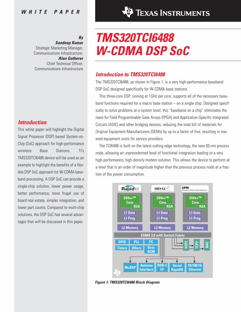
Introduction to TMS320TCI6488The TMS320TCI6488, as shown in Figure 1, is a very high-performance baseband
DSP SoC designed specifically for W-CDMA base stations.
This three-core DSP, running at 1GHz per core, supports all of the necessary base-
band functions required for a macro base station – on a single chip. Designed specif-
ically to solve problems at a system level, this “baseband on a chip” eliminates the
need for Field Programmable Gate Arrays (FPGA) and Application-Specific Integrated
Circuits (ASIC) and other bridging devices, reducing the total bill of materials for
Original Equipment Manufacturers (OEMs) by up to a factor of five, resulting in low-
ered equipment costs for service providers.
The TCI6488 is built on the latest cutting edge technology, the new 65-nm process
node, allowing an unprecedented level of functional integration leading to a very
high-performance, high-density modem solution. This allows the device to perform at
a level that is an order of magnitude higher than the previous process node at a frac-
tion of the power consumption.
W H I T E P A P E R
By Sandeep Kumar
Strategic Marketing Manager,Communications Infrastructure;
Alan GathererChief Technical Officer,
Communications Infrastructure
(Continued next column)
E
n
h
a
n
c
e
d
D
M
A
C
o
n
t
r
o
l
l
e
r
L
2
C
a
c
h
e
M
e
m
o
r
y
5
1
2
K
B
y
t
e
s
E
n
h
a
n
c
e
d
D
M
A
C
o
n
t
r
o
l
l
e
r
L
2
C
a
c
h
e
M
e
m
o
r
y
5
1
2
K
B
y
t
e
s
GPIO PLL I C2
Timers Others BootROM
McBSP AntennaInterface
EDMA 3.0 with Switch Fabric
DDR-2I/F
C64x+™Core
C64x+™Core
C64x+™Core
L1 Data L1 Data L1 DataL1 Prog L1 Prog L1 Prog
L2 Memory L2 Memory L2 Memory
RSA RSA RSA
10/100/1GEthernet
SerialRapidIO
VCP2
TCP2
RAC
Figure 1: TMS320TCI6488 Block Diagram

With a high level of functional integration and a high channel density supported on a
single device, this DSP offers a modular and scalable design with a small footprint.
TCI6488 is a software programmable solution that is upward code-compatible with previ-
ous devices belonging to the C6000 DSP family, and allows for the reuse of existing DSP
software.
Time-to-Market
The time-to-market benefits of using a standard DSP SoC are clear. Eliminating ASIC
design from scratch can lead to significant time savings. In addition, not having to re-spin
one or multiple of the various functional devices in a legacy system can be the difference
between an OEM getting a majority of the market share and missing the market window.
As illustrated in Figure 2 above, being slightly late to market, ensures missing a significant
portion of the revenue and virtually ensures not capturing the entire market when the
product is finally released.
The total revenue lost in this scenario can be calculated as the difference in area
between the two triangles – the red shaded area.
Assuming a constant market ramp, on-time revenue is half (base) × (height)
= 0.5 × Product Lifetime (L) × Maximum Revenue (R) = 0.5 × L × R
And delayed revenue is half (base) × (height)
= 0.5 × Delayed Product lifetime (L–LD) × Delayed Maximum Revenue (RD)
= 0.5 × (L–LD) × RD
Total Revenue Loss is = 0.5 × L × R – 0.5 × (L–LD) × RD = 0.5 × [L × R–(L–LD) × RD]
2 Texas Instruments
TMS320TCI6488 W-CDMA DSP SoC White Paper May 2007
0.5×L L
On-Time SlopeMarketRamp
Late to MarketSlope
Loss Due toLate to Market
R
RD
LDFigure 2: Revenue Lost Due to Delayed Market Entry
GeneralBenefits of
DSP SoC

TMS320TCI6488 W-CDMA DSP SoC White Paper May 2007
3Texas Instruments
Example of Late to Market Revenue Loss
For example, if the total product lifecycle (L) is 48 months, the Max Revenue is $10M per
month, the project delay (LD) = 6 months and the delayed maximum revenue is $7M,
The Total Lost Revenue = 0.5 × (10×48 – (42)×7) = $93M!! (Almost 40% of potential
total revenue from the project)
As can be seen, the revenue lost due to delayed market entry has components of both
delayed market start and inability to hit 100% market share as components of the lost rev-
enue. This does not yet comprehend the additional development expense for the duration
of the delay as well as the lost margin in having to compete for market share when com-
ing from a late-to-market position.
Total Cost of Ownership
Lower Development and Fixed Cost
As can be seen in Figure 3 below, the SoC approach considerably lowers the cost of
development.
The NRE costs associated with developing IP blocks, generating and re-spinning ASIC as
well as testing and qualifying various devices can run in the 10s of millions of dollars.
There is also another component of the initial investment – the additional cost of having
to develop custom prototyping boards for ASIC, as off-the-shelf solutions are not available
with the custom pin-out. DSP SoCs, on the other hand, have a variety of off-the-shelf stan-
dardized board solutions available. These are generally also lower in cost as they are sold
across multiple OEMs and application areas.
Tota
l $ A
mou
nt
NRE & Fixed Cost – Custom
NRE & Fixed Cost – DSP SoC
Total Cost – DSP SoC
Volume
Total Cost – Custom
Total Revenue
Variable Cost – Custom
Breakeven –Custom
Variable Cost – DSP SoC
Breakeven –DSP SoC
Figure 3: Standardized DSP SoCs Lower NRE and Fixed Cost

4 Texas Instruments
TMS320TCI6488 W-CDMA DSP SoC White Paper May 2007
Lower Bill of Materials
In W-CDMA applications, the TCI6488 DSP eliminates the need for ASIC or FPGAs for
chip-rate processing. This results in significant unit cost savings. In addition, through the
integration of standardized system-level interfaces such as Serial RapidIO® and OBSAI, it
also eliminates the need for bridges or glue logic, allowing the device to seamlessly com-
municate with the backplane and a host of other devices. As such, the TCI6488 can lower
the total Bill of Materials (BOM) for a system by up to one-fifth of legacy systems as seen
in Figure 4.
Compared to an all ASIC approach, the DSP SoC approach provides a good balance of
flexibility and cost efficiency. DSP SoCs are used across multiple air-interface standards,
due to their support of multiple standards, and across multiple generations of systems,
due their ability to support emerging features and requirements. Typically, this leads to
DSP SoCs shipping in volumes that exceed what any single custom device would be able
to achieve in isolation. These volumes are leveraged to lower silicon costs and are used to
offer a very attractive price point to help OEMs meet their BOM targets for established
markets, as well as niche and emerging applications.
There are several scenarios where the TCI6488 DSP SoC further demonstrates its ability
to fit into various partitions and resource allocation approaches. In one such example, as
shown previously in Figure 4, the device can be used to construct a 192-user 3GPP
Release 99 system quite easily using four devices. The same device can also be used to
Rx SR
DSP
Rx SR
DSP
Rx CR
DSP
Rx CR
DSP
Rx CR
DSP
Rx CR
DSP
Traditional Rx Card
10
Rx CR
192 DL & UL User Card based on Faraday
EthernetSwitch
(Optional)Traditional Rx CardTraditional Rx Card – 64 Users
Tx SRDSP
Traditional Tx Card – 192 Users
4 – 5 Devices
HostProcessor
HostProcessor
FPGAs/Bridges?
FPGAs/Bridges?
Serial RIO
192 DL & UL User Card Based on Faraday
Bac
kpla
ne to
Rad
io
OBSAI /CPRI
OBSAI /CPRI
TxASIC
Rx SRDSP
10 – 18 Devices Total
Rx CR
DSP Rx CRASIC
OBSAI /CPRI
RapidIOSwitch
(Optional)
Bac
kpla
ne to
Net
wor
k
HostProcessor
TCI6488
DSP
TCI6488
DSP
DSP
TCI6488TCI6488
DSP
Figure 4: TCI6488 Can Reduce BOM Cost by a Factor of 5

TMS320TCI6488 W-CDMA DSP SoC White Paper May 2007
5Texas Instruments
create a High-Speed Downlink Packet Access (HSDPA) system. A virtually complete base-
band system with 192-User, 3-Sector RACH, HSDPA / HSUPA (additional small device
needed for transmit chip rate functionality) can be implemented using just four devices as
seen in Figure 5. This simple example demonstrates how, through software modification,
the same architecture (if not the same channel card) can be used for voice-only users,
HSDPA/HSUPA users, dedicated data users or various combinations of three.
Software Programmable Solution
The move from modems dominated by lots of low data rate voice calls to modems with a
few large data rate data channels that are time multiplexed has actually decreased the
front end signal processing complexity. This is seen conceptually in Figure 6 on the follow-
ing page.
As the data portion of the processing mix on the modem increases, there has been a
steady increase in modem complexity because this processing is correlated with the data
bit rate. On the other hand, the signal processing complexity actually decreased as we
moved away from voice dominated standards and towards time-multiplexed, shared chan-
nels, as used in HSDPA. The addition of antenna arrays and more complicated receiver
structures with HSUPA has increased the complexity of the signal processing. But never-
theless, the role of data processing has increased significantly and this type of processing
has always been done in software. Hence, modems are becoming increasingly soft.
TCI6488
DSP1
TCI6488
DSP2
TCI6488
DSP3
TCI6488
DSP4
GigabitEthernet toNetwork
Backplane
Ethe
rnet
Switc
h
SRIO
SRIO
SRIO
DSP SoC 1, 2, 3:64 UL DCH +
1 cell RACH PD +8 RACH m +64 R.99 SR
DSP SoC 4:3 cell Mac-HS +
3 cell HSDPA SR +192 R.99 SR
AIF to AntennaBackplane
AIF
AIF
AIF
Figure 5: 192-User, 3-Sector RACH, HSDPA/HSUPA on TCI6488

6 Texas Instruments
Software programmability on the baseband, such as that available on the TCI6488, is
becoming more desirable.
By using the TCI6488, OEMs can accelerate their channel card development since it
offers a software-programmable solution and allows for the reuse of existing DSP soft-
ware developed for previous generations of TI infrastructure DSPs. TCI6488 is upward
code-compatible from previous devices that are part of the TMS320C6000™ DSP platform.
Customers can re-use their existing software code base and evolve their system architec-
tures ensuring they get to market more quickly.
Easier Higher Layer Software Provisioning
The main benefit of a system allowing easily provisioned software is quick time to market.
A system using the TCI6488 can provide this benefit in three ways:
Single-Chip Physical Layer Functionality
From the higher layer software perspective, each DSP SoC looks identical and operates at
a user level. This is because a complete user can reside on a single SoC. Therefore the
board-level resource manager does not have to be cognisant of the resource mapping on
the hardware, simplifying resource management. The resource manager on the SoC is in
charge of load balancing the users it is given.
Aggregated MAC Functionality
Traditionally, higher-layer software also has to deal with the task of partitioning physical,
control and signalling as well as MAC layer functionality across separate devices.
SignalProcessing
Dedicated ChannelsMany Fingers
Com
plex
ity
Standards evolution
Scarce SpectrumSingle, Shared chanelHSDPA, OFDM
HSUPA, OFDMAAntenna Arrays, MIMO
Higher DL Data RateMAC Functionality
Higher ULData Rate
DataProcessing
Figure 6: Signal Processing Complexity vs. Standards Evolution

TMS320TCI6488 W-CDMA DSP SoC White Paper May 2007
7Texas Instruments
Typically, the software layers of the modem protocol were separated onto different CPUs,
with the Layer 2 protocol and the board control being implemented on a “control” proces-
sor, usually a PowerPC. One reason for this split was that the control processor devices
had a more suitable peripheral set for communicating with upstream components and had
better software development tools for this type of code.
However, over the last few years, the software development support for Texas
Instruments’ DSPs has improved significantly with industry competitive C, C++ and micro
Linux support. The TMS320C64x+™ CPU used on the TCI6488 also supports memory man-
agement and a user/supervisor mode. TCI6488 supports both Ethernet and Serial RapidIO®
and therefore does not suffer from being “interface poor” for board level and Layer 2
processing.
Greater DSP Horse Power Allows System Homogeneity
With 1-GHz performance per DSP core, the TCI6488 has sufficient processing power on
the three CPUs to absorb the L2 processing and the board control functions on to the DSP
SoC. This gives system designers greater flexibility as to how the software is partitioned.
This has the dual-purpose benefit of simplifying upper-layer software provisioning as well
as reducing the modem board BOM.
Easier Software Replication and System Testing
A direct consequence of the system homogeneity discussed above is that the same physi-
cal layer (and potentially L2) software would be written once and then replicated across
multiple TCI6488 devices making the software development easier and enabling shorter
time-to-market.
Also, since every SoC is self contained, when designing a higher-performance system by
adding more SoCs, the channel card would require little or no testing at the SoC level.
This would mean minimal additional testing at a system level when scaling a system.
Investment Protection via Flexibility
Feature additions and standards evolution are now routinely expected in the wireless
development world. For example, the difference between GPRS and W-CDMA maturity at
deployment is shown in Figure 7 on the following page. A non-editorial change request
(CR) is essentially an engineering “bug” in the standard. Increasingly, standards are
launched early and equipment is deployed with bugs and other uncertainties still present
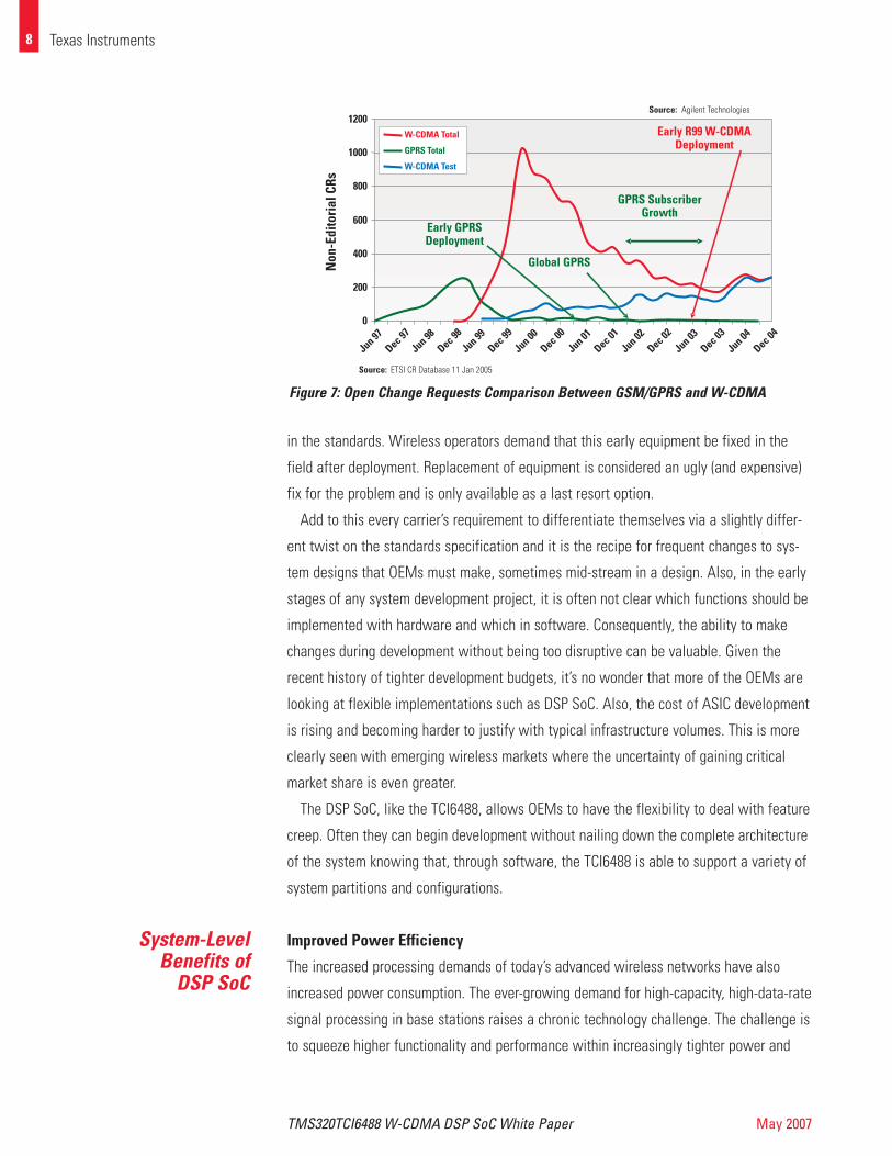
8 Texas Instruments
TMS320TCI6488 W-CDMA DSP SoC White Paper May 2007
in the standards. Wireless operators demand that this early equipment be fixed in the
field after deployment. Replacement of equipment is considered an ugly (and expensive)
fix for the problem and is only available as a last resort option.
Add to this every carrier’s requirement to differentiate themselves via a slightly differ-
ent twist on the standards specification and it is the recipe for frequent changes to sys-
tem designs that OEMs must make, sometimes mid-stream in a design. Also, in the early
stages of any system development project, it is often not clear which functions should be
implemented with hardware and which in software. Consequently, the ability to make
changes during development without being too disruptive can be valuable. Given the
recent history of tighter development budgets, it’s no wonder that more of the OEMs are
looking at flexible implementations such as DSP SoC. Also, the cost of ASIC development
is rising and becoming harder to justify with typical infrastructure volumes. This is more
clearly seen with emerging wireless markets where the uncertainty of gaining critical
market share is even greater.
The DSP SoC, like the TCI6488, allows OEMs to have the flexibility to deal with feature
creep. Often they can begin development without nailing down the complete architecture
of the system knowing that, through software, the TCI6488 is able to support a variety of
system partitions and configurations.
Improved Power Efficiency
The increased processing demands of today’s advanced wireless networks have also
increased power consumption. The ever-growing demand for high-capacity, high-data-rate
signal processing in base stations raises a chronic technology challenge. The challenge is
to squeeze higher functionality and performance within increasingly tighter power and
System-LevelBenefits of
DSP SoC
0
200
400
600
800
1000
1200
Source:
Non
-Edi
tori
al C
RsJun 97
Jun 98
Jun 99
Jun 00
Jun 01
Jun 02
Jun 03
Jun 04
Dec 97
Dec 98
Dec 99
Dec 00
Dec 01
Dec 02
Dec 03
Dec 04
ETSI CR Database 11 Jan 2005
W-CDMA Total
GPRS Total
W-CDMA Test
Source: Agilent Technologies
Early GPRSDeployment
Global GPRS
GPRS SubscriberGrowth
Early R99 W-CDMADeployment
Figure 7: Open Change Requests Comparison Between GSM/GPRS and W-CDMA

TMS320TCI6488 W-CDMA DSP SoC White Paper May 2007
9Texas Instruments
space constraints. As a result, power-performance metrics are now a central concern in
infrastructure system design. New methods have been devised enabling designers to
address the two main areas of power consumption—namely leakage power and dynamic
power—to significantly improve performance compared to conventional techniques.
To solve this problem, the TCI6488 DSP SoC sports a new power and performance man-
agement technology called SmartReflex™. Texas Instruments’ SmartReflex technology is
used to decrease both static and dynamic power consumption while maintaining the spec-
ified device performance.
This technology takes advantage of the fact that a device’s leakage and associated
power can vary significantly across a process distribution as shown in Figure 8.
SmartReflex technology make use of this phenomenon by adjusting the core voltage of
devices to suit the process type of the material.
Another element of SmartReflex technology is enhancing device performance and opti-
mizing power efficiency by considering thermal parameters. To achieve improved power
efficiency, the device implements temperature-dependent dynamic voltage scaling.
The final solution allows full performance utilization of highly integrated silicon designs,
such as TCI6488, with optimized power consumption. A comparison of the 65-nm node
(with and without SmartReflex technology) with the 90-nm node is shown in Figure 9 on
the following page. This allows designers the ability to add multiple TCI6488 devices on a
single card, while still meeting the board power budget.
Another primary component of dynamic power is the chip-to-chip interface between
multiple devices on legacy systems. Through system integration, the DSP SoC approach
ensures that device-to-device communication is kept at a minimum, reducing the overall
system power consumption.
Distributionof Devices
Power
1 GHz
Weaker StrongerProcessStrength
Performance
Figure 8: Device Leakage and Power Can Vary Significantly Across Process Distribution

10 Texas Instruments
TMS320TCI6488 W-CDMA DSP SoC White Paper May 2007
Smaller Form Factor
The efficient integration of the various system-level components on the DSP SoC also
allows for a smaller number of input and output signals (I/Os) and package ball count,
which in turn reduces the size of the device. This has the dual benefit of reducing packag-
ing cost as well as allowing a greater device density on a single board, thus allowing sys-
tem designers to pack more functionality on their board with every generation. The
TCI6488 fits into a small 23 mm × 23 mm flip chip BGA package.
With fewer signals leaving the device, DSP SoCs such as the TCI6488 also have the
added benefit of simplifying board layout and reducing board complexity associated board
cost.
Greater Scalability
According to some analysts, the market for small form factor base stations is on the rise
(see Figure 10).
Relative Power per Function Relative Power per Unit Area
90 nm 90 nm65 nm 65 nm
Process Node Process Node
65 nm withSmartReflex™
65 nm withSmartReflex™
1.4
1.2
1.0
0.8
0.6
0.4
0.2
0.0
3.0
2.5
2.0
1.5
1.0
0.5
0.0
Relative Dynamic Power
Relative Leakage (Static) Power
Relative Dynamic Power
Relative Leakage (Static) Power
Figure 9: 65-nm Node (With and Without SmartReflex) Compared with 90-nm Node
Perc
enta
ge o
f BTS
Shi
pmen
ts 12%
W-CDMA
GSM/GPRS/EDGE
CDMA
9%
6%
3%
0%
2001
2002
2003
2004
2005
2006
2007
2008
2009
2010
Figure 10: Forecast of Pico Base Station as a Percentage of Total Base Stations Shipped
Source: Dell ‘OroMobility ForecastReport 3Q06

TMS320TCI6488 W-CDMA DSP SoC White Paper May 2007
11Texas Instruments
However, the uncertainty around the timing and slope of the pico base station market
ramp make this a questionable market for a custom chip development from the very begin-
ning. As such, a phased approach starting with a standard DSP SoC moving to a custom
SoC is recommended for such markets.
The beauty of a DSP SoC approach is that it allows designers to pick an appropriate
granularity of system performance and then replicate that to match the end system as
shown in Figure 11.
A single TCI6488 can support a complete HSPA pico base station. Thus, software can
be, written, verified and qualified once for such a single DSP SoC to support a pico imple-
mentation and then replicated on top of multiple devices to create larger system configu-
ration, such as micro or macro, in the future. In addition, the availability of high band-
width, peer-to-peer interconnect like Serial RapidIO®, enables OEMs to reduce overall
R&D by allowing it be re-used across form-factor product lines ranging from small enter-
prise class pico base station, all the way to a super macro covering over a 100-Km cell.
Conversely, if the modem designer wishes to dedicate a chip to only one function, such
as Random Access Channel (RACH) messaging, this is also possible with the TCI6488. The
designer can therefore trade off the advantages of code that is repeatable across multiple
devices with the efficiency that might come from concentrating a single function in one
device.
TCI6488
DSP
TCI6488
DSP
TCI6488
DSPMicro
Macro &Super Macro
TCI6488 to TCI6488 data transport via: Serial RapidIO
Antennae data transport via: AIF with daisy chain aggregationNetwork data transport via: Integrated Ethernet
PicoTCI6488
DSP
TCI6488
DSP
TCI6488
DSP
TCI6488
DSP
TCI6488
DSP
TCI6488
DSP
TCI6488
DSP
Figure 11: Standard DSP SoCs Allow for Easy System Scalability

12 Texas Instruments
TMS320TCI6488 W-CDMA DSP SoC White Paper May 2007
Simpler Redundancy and Load Balancing
Inherent in DSP SoC architecture is the built-in multi-function redundancy. Since all the
baseband functions are performed on the TCI6488, system redundancy can be implement-
ed by just adding an additional TCI6488 to the system.
With proper system design, it may be possible to have system redundancy without
adding an additional device. In such cases, the system software would sense if a function-
al unit or logical block on the DSP SoC was not performing and simply switch the task to
another DSP SoC via the Serial RapidIO® subsystem. However, this approach will likely
require the system to drop to a fewer number of supported users.
Via the same approach, the presence of a Serial RapidIO-connected DSP subsystem also
makes it easy for the system to balance the processing load between various DSP SoCs on
the system.
Multi-Standard Support
Back almost a decade ago at the start of the 3G standards development, industry pundits
predicted that the world would converge to one wireless air interface. The mess of stan-
dards that had been 1G had given way to a slightly better situation, at least in Europe,
with 2G, and the hope was that 3G would finish the job. Now, a decade later, this utopian
ideal has been replaced by a fragmented world where multiple standards not only survive
but are being pushed to compete and inter-operate at the same time.
The explosion in the number of wireless air interfaces compounded by a simultaneous
cut back in capital expenditure is forcing OEMs to consider ways to address multiple mar-
ket opportunities while getting the most out of their architecture investments.
This is where TCI6488 comes to the rescue with its ability to support UMTS, GSM, TD-
SCDMA, WiMAX and cdma2000 applications as seen in Figure 12. The three 1-GHZ DSP
Figure 12: TCI6488 Enables Multiple Wireless Modem Standards

TMS320TCI6488 W-CDMA DSP SoC White Paper May 2007
13Texas Instruments
cores go a long way in enabling this device to support multiple standards, while the accel-
eration of the mature, compute intensive W-CDMA functionalities makes sure it is able to
meet the aggressive W-CDMA cost efficiency targets. This flexibility in a small form fac-
tor, scaleable solution provides OEMs a unique solution to support established markets
and extend these into new and emerging infrastructure applications.
Primary W-CDMA Functional Processing
Symbol Rate and MAC-hs Processing
Uplink and downlink symbol rate processing, as well as MAC-hs processing, is performed
on one or more of the three TMS320C64x+™ 1-GHz DSP cores available on the TCI6488.
TCI6488 is upward code-compatible from previous devices that are part of the
TMS320C6000™ DSP platform, with the TCI6488 allowing system designers to re-use their
existing software code base.
In addition, twenty eight (28) new instructions have been added to this DSP core with a
large number of these targeted at improving performance in wireless infrastructure appli-
cations. As such, designers can improve their code performance on a per cycle basis sim-
ply by taking advantage of these new instructions.
FEC Decoding for Voice and Data
The device has two high-performance embedded coprocessors [enhanced Viterbi Decoder
Coprocessor (VCP2) and enhanced Turbo Decoder Coprocessor (TCP2)] that significantly
speed up channel-decoding operations on chip. The VCP2 can decode over 763 12.2-Kbps
adaptive multi-rate (AMR) [K=9, R=1/3] voice channels. The TCP2 can decode up to 44
384-Kbps or 8 2-Mbps turbo encoded channels [assuming 6 iterations].
Both TCP2 and VCP2 are loosely coupled into a DSP subsystem and are fully parameter-
ized to flexibly support various options within the 3GPP specifications. The presence of
VCP2 and TCP2 frees up DSP resources for other processing and enables basebands with
much higher voice and data density than would have been possible with a DSP-only
approach.
Chip-Rate Processing
Transmit Chip-Rate Acceleration Using RSA
Transmit chip-rate processing on the TCI6488 is implemented by a DSP subsystem and its
associated Rake Search/Spread Accelerator (RSA) extensions. These RSA extensions
accelerate CDMA transmit processing by performing the spreading and scrambling func-
tions. The RSA extensions are also capable of carrying out the stream aggregation
W-CDMA-SpecificBenefits of a
DSP SoCApproach

14 Texas Instruments
TMS320TCI6488 W-CDMA DSP SoC White Paper May 2007
functionality Also, in conjunction with the DSP cores, they can also perform search func-
tionality that can be used to augment the Preamble Detect (PD) and Path Monitoring (PM)
functions typically performed on the Receive Accelerator.
The RSA extensions allow the TCI6488 to truly shine in supporting very high user densi-
ty, multiple antennas, variety of data formats as well as an array of system configurations.
Thus a base station using the TCI6488 can flexibly support multiple voice and data users,
as well as cell sizes over 100 miles in size. All of this is accomplished without sacrificing
cost or power efficiency, in large part due to the RAC.
Figure 13 shows the functional split of transmit chip-rate processing between the DSP
subsystem and the RSA extensions. The DSP core generates both OVSF and PN codes and
provides the multiplied result of these two codes as input to the RSA. The modulated user
symbols are also provided as input to the RSA. The RSA applies the code values to the
modulated symbols to achieve spreading and scrambling.
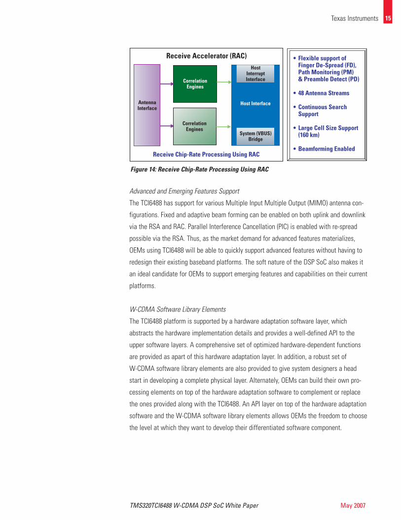
Receive Chip-Rate Acceleration Using RAC
Receive chip-rate processing on the TCI6488 is implemented via the Receive DSP core and
the Receive Accelerator (RAC). The RAC is comprised of highly flexible and programmable
correlation engines, as shown in Figure 14. These can be configured to carry out various
receive chip-rate functions, including Rake finger de-spreading (FD), EOL finger tracking
(FT), search or path monitoring (PM) operations and RACH preamble detection (PD) opera-
tions. These blocks receive 2× over sampled chip-rate antenna streams and provide the Rx
accelerator DSP with either de-spread symbols or correlation energies. These blocks sup-
port a very large amount of correlation resources and can support up to 6,144 32-chip cor-
relations per 32-chip period. The DSP associated with the RAC serves to control and con-
figure the two correlation engines.
DSPSystem
OVSF and PNCode Generation
384 channels24 antennastreamsMIMO andbeamformingenabled
••
•
1-Bit I,1-Bit Q
EFI
EFI 32-Bit I,32-Bit Q
L2 Memory(User Symbols)
RSAMultiply
andAccumulate
ModulationApply Closed-Loop Gain
Apply Power-Control Gain
Figure 13: Functional DSP and RSA Split for Transmit Chip-Rate Processing
TMS320TCI6488 W-CDMA DSP SoC White Paper May 2007
15Texas Instruments
Advanced and Emerging Features Support
The TCI6488 has support for various Multiple Input Multiple Output (MIMO) antenna con-
figurations. Fixed and adaptive beam forming can be enabled on both uplink and downlink
via the RSA and RAC. Parallel Interference Cancellation (PIC) is enabled with re-spread
possible via the RSA. Thus, as the market demand for advanced features materializes,
OEMs using TCI6488 will be able to quickly support advanced features without having to
redesign their existing baseband platforms. The soft nature of the DSP SoC also makes it
an ideal candidate for OEMs to support emerging features and capabilities on their current
platforms.
W-CDMA Software Library Elements
The TCI6488 platform is supported by a hardware adaptation software layer, which
abstracts the hardware implementation details and provides a well-defined API to the
upper software layers. A comprehensive set of optimized hardware-dependent functions
are provided as apart of this hardware adaptation layer. In addition, a robust set of
W-CDMA software library elements are also provided to give system designers a head
start in developing a complete physical layer. Alternately, OEMs can build their own pro-
cessing elements on top of the hardware adaptation software to complement or replace
the ones provided along with the TCI6488. An API layer on top of the hardware adaptation
software and the W-CDMA software library elements allows OEMs the freedom to choose
the level at which they want to develop their differentiated software component.
CorrelationEngines
Receive Accelerator (RAC)
CorrelationEngines
Host InterfaceAntennaInterface
Receive Chip-Rate Processing Using RAC
Flexible support ofFinger De-Spread (FD),Path Monitoring (PM)& Preamble Detect (PD)
48 Antenna Streams
Continuous SearchSupport
Large Cell Size Support(160 km)
Beamforming Enabled
•
•
•
•
•
HostInterruptInterface
System (VBUS)Bridge
Figure 14: Receive Chip-Rate Processing Using RAC

16 Texas Instruments
TMS320TCI6488 W-CDMA DSP SoC White Paper May 2007
W-CDMA on DSP SoC Architecture Considerations
Introduction
A base station modem is a real-time system with multiple users, all with their own real-
time constraints, being supported simultaneously. Recent modems that support data trans-
fer have the added complexity of having to support many different users with different
data rates and QoS requirements leading to differing I/O, MIPS, and memory require-
ments. In order to understand the benefits of the DSP SoC approach for W-CDMA base
stations, it is pertinent to consider the trade-offs made by designers when designing a
multi-user modem.
For the purposes of this discussion, a simplified receiver (demodulation) modem data
flow is considered, as shown in Figure 15, which includes both a low latency control path
and a higher latency data path.
Additionally, every system is assumed to have at least a basic Real-Time Operating
System (RTOS) to schedule tasks and users.
Task Division
One of the basic decisions concerning whether a basic software task can be performed
relates to a user or a function, as seen in Figure 16. This decision impacts the way
filter
demod FEC unpack
demod FEC unpack
data
control
Figure 15: Simplified Receiver Modem Data Flow
Filt1
D_slow1
Filt2
F_slow1
F_slow2
U_slow1
U_slow2
D_fast1 D_fast1
D_fast2 D_fast2
U_fast1
U_fast2 U_fast2
F_fast1
F_fast2 F_fast2
Tasks Split by User Tasks Split by Function
D_slow2 F_slow2 U_slow2D_slow2
Filt1
Filt2
D_slow1 U_slow1F_slow1
U_fast1F_fast1
Figure 16: Processing Tasks Split by User and Function

TMS320TCI6488 W-CDMA DSP SoC White Paper May 2007
17Texas Instruments
interrupts are generated and how often tasks switch. It also affects the way software
interacts with any peripherals and hardware acceleration on the DSP SoC.
Dividing Tasks by Users
If the tasks are divided by users, the RTOS will not know how many tasks will be present
at any given time. The main issue with dividing the tasks by user is that the number of
tasks grows with the number of users. For instance, on a macro base station, there may be
up to 64 users running on a TCI6488 and these users may require multiple tasks each.
Also, as the number of tasks grows, so generally will the number of task switches per sec-
ond. Not only is there a crushing number of task structures to manage, but also more time
will be spent in interrupt routines and in the kernel, and less time doing useful work.
Typically, this can lead to an unmanageable system above a few tens of users.
Dividing Tasks by Functions
If the tasks are divided by functions, the RTOS does not have to know how many users are
present in the system. It only has to know how many unique functions are to be per-
formed. As the number of users increases, the time it takes a task to complete will
increase as that task will run for each user that needs that task at that point in time. If the
task is called immediately, when there is data available for each task, then each task will
be called for each user and the number of task switches will increase with the number of
users. This can again lead to a crushing number of task switches.
A Hybrid Approach
A better way to manage this is to assign each task to a linked list. When a task runs to
completion, for each user, it will add an item to the linked list of the task associated with
the next function to be performed on that user. This will not cause an interrupt to be gen-
erated and the users will accumulate on the linked list. At some point the task will be
activated and it will process its linked list to completion, or until it is pre-empted.This
method of task definition and processing is generally preferred on the TCI6488.
Key Take-Away From the User and Task Grouping Analysis
In order to keep the number of tasks, and the task pre-emption overhead, to a manageable
level, they must not scale with the number of users. Tasks should be associated with func-
tions and not users. This can be done by setting up a number of queues. Tasks are
18 Texas Instruments
TMS320TCI6488 W-CDMA DSP SoC White Paper May 2007
associated with a queue (usually several tasks per queue) and requests for operation of a
task on a particular user are linked to these queues. The kernel will manage the draining
of these queues and can do this in several ways, using periodic or data-driven interrupts
to achieve real-time operation. As mentioned earlier, this is the recommended approach
when using the TCI6488 for W-CDMA applications.
Scheduling on a Multi-Core DSP SoC with Acceleration
Having considered how to group tasks and users on the TCI6488, the question naturally
arises of how to map users and task on a DSP SoC. The TCI6488 is a multi-CPU DSP SoC
and composed of independent IP blocks that interoperate and synchronize to achieve a sin-
gle complete modem function. As such, mapping the priority queue into a multi-CPU envi-
ronment is an important consideration when designing W-CDMA systems using it.
Mapping Users Across DSP SoC CPUs
One simple way to do this is to divide the users amongst the CPUs, so that each CPU
maintains its own queues. However, some functions, such as filtering and demodulation,
may be shared amongst all users. Also, some functions may be required to share
coprocessors or peripherals, and are therefore interdependent.
In this case, the interaction between the sets of priority queues can get quite complicat-
ed and it gets difficult to ensure real-time performance. Also, the complexity of the
coprocessors and peripherals increases because they have to support multiple CPUs. This
involves making decisions about priority of tasks from different CPUs. All this adds com-
plexity to hardware and also to software drivers. It also makes testing of the final system
more complex.
Mapping Tasks across DSP SoC CPUs
Another approach is one of assigning a functional task to a single CPU so that each CPU is
in charge of a unique group of functions. Each coprocessor, which generally accelerates a
specific type of function, is associated with a single CPU and control of the order of tasks
performed on that coprocessor is significantly simplified. In many cases peripherals will
only communicate with a single CPU as well. This reduces the testing required to verify
that tasks will not be starved of data.
Synchronization between CPUs can be achieved by system-wide synchronization signals
that align the CPUs to frame, slot and symbol boundaries. Communication between CPUs
is in the form of blocks of data generated by one task and destined for another via Direct

TMS320TCI6488 W-CDMA DSP SoC White Paper May 2007
19Texas Instruments
Memory Access (DMA) approach between L2 memories. This is the recommended
approach when using the TCI6488.
Recommended Resource Mapping with TCI6488
The architecture of the TCI6488 has been kept as symmetrical as possible so that it may
be used with a variety of functional splits and system partitions. All DSP cores have
access to the Receive accelerator, for instance. It is therefore possible to run the same
functions on all CPUs, and have all CPUs access all coprocessor and peripheral resources.
Yet, it is noted that simplicity of software architecture, along with the nature of many
modem algorithms, leads the smart system designer to partition the tasks so that the soft-
ware is not symmetric across CPUs. This is why despite the symmetric architecture, there
is still a recommended usage model, the outcome of extensive study of code cycle esti-
mates, spreadsheet analysis and transactional level models.
Based on this analysis, software partition recommended for W-CDMA allows the sim-
plicity of having only one CPU controlling the RAC, one CPU controlling the TCP and VCP,
and one CPU performing transmit chip-rate function as well as communication with the
antenna array interface for output. Each CPU is also equipped with its own L2 memory as
is appropriate in an implementation where each CPU has a unique function. This simplifies
the operation of the device and allows the system designer to extract maximum applica-
tion level efficiency from the device.
For other standards, such as those based on OFDM, the natural inclination may be to
use a symmetrical software architecture. But even in this case, it is recommended to
divide the problem so that certain functions, such as FFT/IFFT and some modulation and
demodulation is performed by one CPU and the results communicated to another CPU for
symbol-rate processing. In fact, in the case of OFDMA, the modulation is jointly performed
for all users and users cannot be completely separated onto different CPUs. This certainly
simplifies communication between the antenna interface (or Serial RapidIO® if this is
used for antenna data) and the CPU processing the front end. This also has the added ben-
efit of simplifying the back-end symbol-rate processing and its communication with the
network interface.
Balancing Resources on a Multi-DSP SoC System
As it was recommended in the previous section that each CPU perform different tasks
from each other, it is worthwhile considering if the same approach can be extended to
each DSP SoC having a different task in a multi-DSP system. For instance, a scenario can

20 Texas Instruments
TMS320TCI6488 W-CDMA DSP SoC White Paper May 2007
be imagined in which there would be one DSP SoC performing nothing but symbol-rate
decode and one DSP SoC performing nothing but chip-rate modulation.
In a purely soft implementation, this makes sense. However, in such a scenario, any co-
processing elements present on chip will not be used efficiently. For instance on a
TCI6488, performing only symbol-rate processing needs a powerful set of VCP2 and TCP2
engines, as present. However, on another DSP SoC performing only chip-rate tasks, the
VCP2 and TCP2 engines would be unused.
Thus, dedicating DSP SoCs to a particular subset of functions also does not make for a
scalable system. Clearly, if one wishes to increase the channel density on a board, with
each SoC performing the same complete set of functions, one can simply add more SoCs
to the board. The TCI6488 is designed to allow this to happen with the minimal extra hard-
ware. The Antenna Interface (AIF) and Serial RapidIO® both can be connected in a daisy
chain configuration to enable multi-device systems. The gigabit Ethernet and Serial RapidIO
interfaces can also be attached to a switch to create a scaleable fabric-based system.
Handling of W-CDMA Tighter Latency on DSP SoC
Compared to a design where each device performs a different task, DSP SoC has the
advantage of latency in transferring data from task to task, while executing the data path
of one user is smaller because the data is kept contained on chip.
System Architecture Conclusion
For a system design using DSP SoCs, such as TCI6488, the system architecture that is the
most scalable at the board level and leads to the simplest, most easily tested software is
one in which each CPU in the DSP SoC performs a unique subset of tasks, but each SoC in
the system performs the same set of tasks as the other SoCs. TCI6488 has been optimized
for this scenario for W-CDMA/HSPA, but is flexible enough to also efficiently support
other modem standards and partitions.
The goal for any SoC is to have the perfect balance of on-chip resources. Therefore, prop-
erly sizing memory, IO, CPU and other resources from the outset is critical. Comprehending
and balancing resource requirements on a DSP SoC requires a good grasp of the end sys-
tem as well as a clear understanding of the real-time constraints. Failure to understand
real-time requirements can be disastrous and lead to resource underutilization, insufficient
capacity, bandwidth, memory or a combination of these. Sharing hardware resources and
multiple threads or services allocated to multiple processor cores increases complexity
and risk. Up-front understanding and avoidance of known resource sharing pitfalls is
Challenges tothe DSP SoC
Approach

21Texas Instruments
strongly suggested. When multiple resources must be shared, interaction should be well
synchronized, brief and well tested.
How TCI6488 Guards Against Typical SoC Pitfalls
Though the TCI6488 was designed from the ground-up to be a very effective real time
W-CDMA baseband processor, it still incorporates features to help the system designer,
should one of the typical problems listed above occur.
• Insufficient memory – In addition to the hefty on-chip memory already included, the
TCI6488 also allows for a variety of external memory devices supported through its
DDR-2 memory interface.
• Inadequate acceleration – The presence of Serial RapidIO® allows for a very-high band-
width, low-latency option for connectivity to external accelerators, including those
implemented on FPGAs.
• Insufficient performance – Multiple copies of the TCI6488 can be instantiated. Given the
re-use of the software and the ease of connectivity via Serial RapidIO, getting to the
right performance is easier than ever.
The value in a DSP SoC approach lies in its ability to provide time-to-market advantages
without sacrificing BOM savings. The ease of software provisioning and testing eases the
burden on system software. The software programmable nature of TCI6488 helps insulate
OEMs and carriers against unanticipated changes, while allowing them to leverage their
existing code base. The ease of software replication and the enhanced device features,
along with power efficiency and small form factor, allow system designers to easily scale
their designs to meet application requirements. DSP SoCs are also particularly well suited
to allow implementation of redundancy and load balancing. Via hardware and software
mechanisms, well-designed DSP SoCs, like the TCI6488, also avoid the typical pitfalls that
can plague SoCs.
TCI6488 DSP offers a high-performance, power-efficient and cost-effective baseband
platform capable of supporting physical layer processing, including symbol-rate and chip-
rate processing. Designed specifically for the W-CDMA base station, the TCI6488 helps
designers achieve unprecedented system density and performance.
Summary andConclusion
SPRAAM8© 2007 Texas Instruments IncorporatedPrinted in the U.S.A.
Important Notice: The products and services of Texas Instruments Incorporated and its subsidiaries described herein are sold subject to TI’s standard terms and conditions of sale. Customers are advised to obtain the most current and complete information about TI products and services before placing orders. TI assumes noliability for applications assistance, customer’s applications or product designs, software performance, or infringement of patents. The publication of informationregarding any other company’s products or services does not constitute TI’s approval, warranty or endorsement thereof.
All trademarks are the property of their respective owners.

IMPORTANT NOTICE
Texas Instruments Incorporated and its subsidiaries (TI) reserve the right to make corrections, modifications, enhancements,improvements, and other changes to its products and services at any time and to discontinue any product or service without notice.Customers should obtain the latest relevant information before placing orders and should verify that such information is current andcomplete. All products are sold subject to TI’s terms and conditions of sale supplied at the time of order acknowledgment.
TI warrants performance of its hardware products to the specifications applicable at the time of sale in accordance with TI’sstandard warranty. Testing and other quality control techniques are used to the extent TI deems necessary to support thiswarranty. Except where mandated by government requirements, testing of all parameters of each product is not necessarilyperformed.
TI assumes no liability for applications assistance or customer product design. Customers are responsible for their products andapplications using TI components. To minimize the risks associated with customer products and applications, customers shouldprovide adequate design and operating safeguards.
TI does not warrant or represent that any license, either express or implied, is granted under any TI patent right, copyright, maskwork right, or other TI intellectual property right relating to any combination, machine, or process in which TI products or servicesare used. Information published by TI regarding third-party products or services does not constitute a license from TI to use suchproducts or services or a warranty or endorsement thereof. Use of such information may require a license from a third party underthe patents or other intellectual property of the third party, or a license from TI under the patents or other intellectual property of TI.
Reproduction of information in TI data books or data sheets is permissible only if reproduction is without alteration and isaccompanied by all associated warranties, conditions, limitations, and notices. Reproduction of this information with alteration is anunfair and deceptive business practice. TI is not responsible or liable for such altered documentation.
Resale of TI products or services with statements different from or beyond the parameters stated by TI for that product or servicevoids all express and any implied warranties for the associated TI product or service and is an unfair and deceptive businesspractice. TI is not responsible or liable for any such statements.
TI products are not authorized for use in safety-critical applications (such as life support) where a failure of the TI product wouldreasonably be expected to cause severe personal injury or death, unless officers of the parties have executed an agreementspecifically governing such use. Buyers represent that they have all necessary expertise in the safety and regulatory ramificationsof their applications, and acknowledge and agree that they are solely responsible for all legal, regulatory and safety-relatedrequirements concerning their products and any use of TI products in such safety-critical applications, notwithstanding anyapplications-related information or support that may be provided by TI. Further, Buyers must fully indemnify TI and itsrepresentatives against any damages arising out of the use of TI products in such safety-critical applications.
TI products are neither designed nor intended for use in military/aerospace applications or environments unless the TI products arespecifically designated by TI as military-grade or "enhanced plastic." Only products designated by TI as military-grade meet militaryspecifications. Buyers acknowledge and agree that any such use of TI products which TI has not designated as military-grade issolely at the Buyer's risk, and that they are solely responsible for compliance with all legal and regulatory requirements inconnection with such use.
TI products are neither designed nor intended for use in automotive applications or environments unless the specific TI productsare designated by TI as compliant with ISO/TS 16949 requirements. Buyers acknowledge and agree that, if they use anynon-designated products in automotive applications, TI will not be responsible for any failure to meet such requirements.
Following are URLs where you can obtain information on other Texas Instruments products and application solutions:
Products Applications
Amplifiers amplifier.ti.com Audio www.ti.com/audio
Data Converters dataconverter.ti.com Automotive www.ti.com/automotive
DSP dsp.ti.com Broadband www.ti.com/broadband
Interface interface.ti.com Digital Control www.ti.com/digitalcontrol
Logic logic.ti.com Military www.ti.com/military
Power Mgmt power.ti.com Optical Networking www.ti.com/opticalnetwork
Microcontrollers microcontroller.ti.com Security www.ti.com/security
RFID www.ti-rfid.com Telephony www.ti.com/telephony
Low Power www.ti.com/lpw Video & Imaging www.ti.com/videoWireless
Wireless www.ti.com/wireless
Mailing Address: Texas Instruments, Post Office Box 655303, Dallas, Texas 75265Copyright © 2007, Texas Instruments Incorporated


![Verilog design example [相容模式] - SOC & DSP Labsocdsp.ee.nchu.edu.tw/class/download/vlsi_dsp_102/night/DSP/Veril… · Verilog HDL Code(part 1): Symbol view: Verilog HDL](https://img.pdfslide.net/doc/110x75/5f8b5fb5089abf43c543d928/verilog-design-example-c-soc-dsp-verilog-hdl-codepart-1i.jpg)