Embed Size (px)
Citation preview

System Inputs &
Sensors
LDO #1
D
S1
S2
S3
S4
S5
S6
S7
S8
Integrated
12-bit ADC
A0A1 A2
ENMCU
LDO #2
LM20
Analog Temp.
Sensor
LM20
Analog Temp.
SensorGND
VDD
VDDVDD VI/O
1.8V Logic I/O
LM20
Analog Temp.
Sensor
LDO #3RAM FLASH
Port I/O TIMERS
TMUX1208
A0 A1 A2 EN
S1
D
S2S3S4S5S6S7S8
1-OF-8DECODER
TMUX1209
S1A
DB
S2AS3AS4A
S1BS2BS3BS4B
DA
A0 A1 EN
1-OF-4DECODER
Product
Folder
Order
Now
Technical
Documents
Tools &
Software
Support &Community
An IMPORTANT NOTICE at the end of this data sheet addresses availability, warranty, changes, use in safety-critical applications,intellectual property matters and other important disclaimers. PRODUCTION DATA.
TMUX1208, TMUX1209SCDS389C –AUGUST 2018–REVISED DECEMBER 2018
TMUX1208 5-V Bidirectional 8:1, 1-Channel MultiplexerTMUX1209 5-V Bidirectional 4:1, 2-Channel Multiplexer
1
1 Features1• Rail to Rail Operation• Bidirectional Signal Path• Low On-Resistance: 5 Ω• Wide Supply Range: 1.08 V to 5.5 V• -40°C to +125°C Operating Temperature• 1.8 V Logic Compatible• Fail-Safe Logic• Low Supply Current: 10 nA• Transition Time: 14 ns• Break-Before-Make Switching• ESD Protection HBM: 2000 V• Industry-Standard TSSOP and QFN Packages
2 Applications• Analog and Digital Multiplexing / Demultiplexing• HVAC: Heating, Ventilation, and Air Conditioning• Smoke Detectors• Video Surveillance• Electronic Point of Sale• Battery-Powered Equipment• Appliances• Consumer Audio
3 DescriptionThe TMUX1208 and TMUX1209 are general purposecomplementary metal-oxide semiconductor (CMOS)multiplexers (MUX). The TMUX1208 offers 8:1 single-ended channels, while the TMUX1209 offersdifferential 4:1 or dual 4:1 single-ended channels.Wide operating supply of 1.08 V to 5.5 V allows foruse in a broad array of applications from personalelectronics to building automation applications. Thedevice supports bidirectional analog and digitalsignals on the source (Sx) and drain (D) pins rangingfrom GND to VDD.
All logic inputs have 1.8 V logic compatiblethresholds, ensuring both TTL and CMOS logiccompatibility when operating in the valid supplyvoltage range. Fail-Safe Logic circuitry allowsvoltages on the control pins to be applied before thesupply pin, protecting the device from potentialdamage.
Device Information(1)
PART NUMBER PACKAGE BODY SIZE (NOM)
TMUX1208TMUX1209
TSSOP (16) 5.00 mm × 4.40 mmQFN (16) 2.60 mm x 1.80 mm
(1) For all available packages, see the package option addendumat the end of the data sheet.
SPACER
Application Example TMUX1208, TMUX1209 Block Diagram

2
TMUX1208, TMUX1209SCDS389C –AUGUST 2018–REVISED DECEMBER 2018 www.ti.com
Product Folder Links: TMUX1208 TMUX1209
Submit Documentation Feedback Copyright © 2018, Texas Instruments Incorporated
Table of Contents1 Features .................................................................. 12 Applications ........................................................... 13 Description ............................................................. 14 Revision History..................................................... 25 Device Comparison Table ..................................... 36 Pin Configuration and Functions ......................... 37 Specifications......................................................... 5
7.1 Absolute Maximum Ratings ...................................... 57.2 ESD Ratings.............................................................. 57.3 Recommended Operating Conditions....................... 57.4 Thermal Information .................................................. 57.5 Electrical Characteristics (VDD = 5 V ±10 %)............ 67.6 Electrical Characteristics (VDD = 3.3 V ±10 %)......... 87.7 Electrical Characteristics (VDD = 1.8 V ±10 %)....... 107.8 Electrical Characteristics (VDD = 1.2 V ±10 %)....... 127.9 Typical Characteristics ............................................ 14
8 Detailed Description ............................................ 158.1 Overview ................................................................. 158.2 Functional Block Diagram ....................................... 208.3 Feature Description................................................. 20
9 Application and Implementation ........................ 229.1 Application Information............................................ 229.2 Typical Application ................................................. 229.3 Design Requirements.............................................. 229.4 Detailed Design Procedure ..................................... 239.5 Application Curve .................................................... 23
10 Power Supply Recommendations ..................... 2311 Layout................................................................... 24
11.1 Layout Guidelines ................................................. 2411.2 Layout Example .................................................... 24
12 Device and Documentation Support ................. 2512.1 Documentation Support ........................................ 2512.2 Related Links ........................................................ 2512.3 Receiving Notification of Documentation Updates 2512.4 Community Resources.......................................... 2512.5 Trademarks ........................................................... 2512.6 Electrostatic Discharge Caution............................ 2512.7 Glossary ................................................................ 25
13 Mechanical, Packaging, and OrderableInformation ........................................................... 25
4 Revision HistoryNOTE: Page numbers for previous revisions may differ from page numbers in the current version.
Changes from Revision B (November 2018) to Revision C Page
• Added device TMUX1209 to the data sheet ......................................................................................................................... 1
Changes from Revision A (September 2018) to Revision B Page
• Added RSV (QFN) thermal information to Thermal Information: table................................................................................... 5• Added footnote to clarify test conditions ................................................................................................................................ 8
Changes from Original (August 2018) to Revision A Page
• Changed the document status From: Advanced Information To: Production data ................................................................ 1

1N.C.
2S1
3S2
4S3
5S
4
6D
7S
8
8S
7
9 S6
10 S5
11 VDD
12 GND
13A
2
14A
1
15A
0
16E
N
No t to scale
1A0 16 A1
2EN 15 A2
3N.C. 14 GND
4S1 13 VDD
5S2 12 S5
6S3 11 S6
7S4 10 S7
8D 9 S8
Not to scale
3
TMUX1208, TMUX1209www.ti.com SCDS389C –AUGUST 2018–REVISED DECEMBER 2018
Product Folder Links: TMUX1208 TMUX1209
Submit Documentation FeedbackCopyright © 2018, Texas Instruments Incorporated
5 Device Comparison Table
PRODUCT DESCRIPTIONTMUX1208 8:1, 1-Channel, single-ended multiplexerTMUX1209 4:1, 2-Channel, differential multiplexer
6 Pin Configuration and Functions
TMUX1208: PW Package16-Pin TSSOP
Top ViewTMUX1208: RSV Package
16-Pin QFNTop View
(1) I = input, O = output, I/O = input and output, P = power
Pin Functions TMUX1208PIN
TYPE (1) DESCRIPTIONNAME TSSOP UQFN
A0 1 15 I Address line 0. Controls the switch configuration as shown in Table 1.
EN 2 16 I Active high logic input. When this pin is low, all switches are turned off. When this pin is high,the A[2:0] address inputs determine which switch is turned on.
N.C. 3 1 Not Connected Not Connected
S1 4 2 I/O Source pin 1. Can be an input or output.
S2 5 3 I/O Source pin 2. Can be an input or output.
S3 6 4 I/O Source pin 3. Can be an input or output.
S4 7 5 I/O Source pin 4. Can be an input or output.
D 8 6 I/O Drain pin. Can be an input or output.
S8 9 7 I/O Source pin 8. Can be an input or output.
S7 10 8 I/O Source pin 7. Can be an input or output.
S6 11 9 I/O Source pin 6. Can be an input or output.
S5 12 10 I/O Source pin 5. Can be an input or output.
VDD 13 11 P Positive power supply. This pin is the most positive power-supply potential. For reliableoperation, connect a decoupling capacitor ranging from 0.1 µF to 10 µF between VDD and GND.
GND 14 12 P Ground (0 V) reference
A2 15 13 I Address line 2. Controls the switch configuration as shown in Table 1.
A1 16 14 I Address line 1. Controls the switch configuration as shown in Table 1.

1N.C.
2S1A
3S2A
4S3A
5S
4A
6D
A
7D
B
8S
4B
9 S3B
10 S2B
11 S1B
12 VDD
13
GN
D
14
A1
15
A0
16
EN
Not to scale
1A0 16 A1
2EN 15 GND
3N.C. 14 VDD
4S1A 13 S1B
5S2A 12 S2B
6S3A 11 S3B
7S4A 10 S4B
8DA 9 DB
Not to scale
4
TMUX1208, TMUX1209SCDS389C –AUGUST 2018–REVISED DECEMBER 2018 www.ti.com
Product Folder Links: TMUX1208 TMUX1209
Submit Documentation Feedback Copyright © 2018, Texas Instruments Incorporated
TMUX1209: PW Package16-Pin TSSOP
Top ViewTMUX1209: RSV Package
16-Pin QFNTop View
(1) I = input, O = output, I/O = input and output, P = power
Pin Functions TMUX1209PIN
TYPE (1) DESCRIPTIONNAME TSSOP UQFN
A0 1 15 I Address line 0. Controls the switch configuration as shown in Table 2.
EN 2 16 I Active high logic input. When this pin is low, all switches are turned off. When this pin is high,the A[1:0] address inputs determine which switch is turned on.
N.C. 3 1 Not Connected Not Connected
S1A 4 2 I/O Source pin 1A. Can be an input or output.
S2A 5 3 I/O Source pin 2A. Can be an input or output.
S3A 6 4 I/O Source pin 3A. Can be an input or output.
S4A 7 5 I/O Source pin 4A. Can be an input or output.
DA 8 6 I/O Drain pin A. Can be an input or output.
DB 9 7 I/O Drain pin B. Can be an input or output.
S4B 10 8 I/O Source pin 4B. Can be an input or output.
S3B 11 9 I/O Source pin 3B. Can be an input or output.
S2B 12 10 I/O Source pin 2B. Can be an input or output.
S1B 13 11 I/O Source pin 1B. Can be an input or output.
VDD 14 12 P Positive power supply. This pin is the most positive power-supply potential. For reliableoperation, connect a decoupling capacitor ranging from 0.1 µF to 10 µF between VDD and GND.
GND 15 13 P Ground (0 V) reference
A1 16 14 I Address line 1. Controls the switch configuration as shown in Table 2.

5
TMUX1208, TMUX1209www.ti.com SCDS389C –AUGUST 2018–REVISED DECEMBER 2018
Product Folder Links: TMUX1208 TMUX1209
Submit Documentation FeedbackCopyright © 2018, Texas Instruments Incorporated
(1) Stresses beyond those listed under Absolute Maximum Rating may cause permanent damage to the device. These are stress ratingsonly, which do not imply functional operation of the device at these or any other conditions beyond those indicated under RecommendedOperating Condition. Exposure to absolute-maximum-rated conditions for extended periods may affect device reliability.
(2) The algebraic convention, whereby the most negative value is a minimum and the most positive value is a maximum.(3) All voltages are with respect to ground, unless otherwise specified.
7 Specifications
7.1 Absolute Maximum Ratingsover operating free-air temperature range (unless otherwise noted) (1) (2) (3)
MIN MAX UNITVDD Supply voltage –0.3 6 VVSEL or VEN Logic control input pin voltage (EN, A0, A1, A2) –0.3 6 VISEL or IEN Logic control input pin current (EN, A0, A1, A2) –30 30 mAVS or VD Source or drain voltage (Sx, D) –0.5 VDD+0.5 VIS or ID (CONT) Source or drain continuous current (Sx, D) –30 30 mATstg Storage temperature –65 150 °CTJ Junction temperature 150 °C
(1) JEDEC document JEP155 states that 500-V HBM allows safe manufacturing with a standard ESD control process.(2) JEDEC document JEP157 states that 250-V CDM allows safe manufacturing with a standard ESD control process.
7.2 ESD RatingsVALUE UNIT
V(ESD) Electrostatic discharge
Human body model (HBM), perANSI/ESDA/JEDEC JS-001, all pins (1) ±2000
VCharged device model (CDM), per JEDECspecification JESD22-C101, all pins (2) ±750
7.3 Recommended Operating Conditionsover operating free-air temperature range (unless otherwise noted)
MIN NOM MAX UNITVDD Supply voltage 1.08 5.5 VVS or VD Signal path input/output voltage (source or drain pin) (Sx, D) 0 VDD VVSEL orVEN
Logic control input pin voltage (EN, A0, A1, A2) 0 5.5 V
TA Ambient temperature –40 125 °C
7.4 Thermal Information
THERMAL METRICTMUX1208 / TMUX1209
UNITPW (TSSOP) RSV (QFN)16 PINS 16 PINS
RθJA Junction-to-ambient thermal resistance 118.9 134.6 °C/WRθJC(top) Junction-to-case (top) thermal resistance 49.3 74.3 °C/WRθJB Junction-to-board thermal resistance 65.2 62.8 °C/WΨJT Junction-to-top characterization parameter 7.6 4.3 °C/WΨJB Junction-to-board characterization parameter 64.6 61.1 °C/WRθJC(bot) Junction-to-case (bottom) thermal resistance N/A N/A °C/W

6
TMUX1208, TMUX1209SCDS389C –AUGUST 2018–REVISED DECEMBER 2018 www.ti.com
Product Folder Links: TMUX1208 TMUX1209
Submit Documentation Feedback Copyright © 2018, Texas Instruments Incorporated
(1) When VS is 4.5 V, VD is 1 V, and vice versa.
7.5 Electrical Characteristics (VDD = 5 V ±10 %)at TA = 25°C, VDD = 5 V (unless otherwise noted)
PARAMETER TEST CONDITIONS TA MIN TYP MAX UNITANALOG SWITCH
RON On-resistanceVS = 0 V to VDDISD = 10 mARefer to On-Resistance
25°C 5 Ω
–40°C to +85°C 7 Ω
–40°C to +125°C 9 Ω
ΔRONOn-resistance matching betweenchannels
VS = 0 V to VDDISD = 10 mARefer to On-Resistance
25°C 0.15 Ω
–40°C to +85°C 1 Ω
–40°C to +125°C 1 Ω
RONFLAT
On-resistance flatnessVS = 0 V to VDDISD = 10 mARefer to On-Resistance
25°C 1.5 Ω
–40°C to +85°C 2 Ω
–40°C to +125°C 3 Ω
IS(OFF) Source off leakage current (1)
VDD = 5 VSwitch OffVD = 4.5 V / 1 VVS = 1 V / 4.5 VRefer to Off-Leakage Current
25°C ±75 nA–40°C to +85°C -150 150 nA
–40°C to +125°C -175 175 nA
ID(OFF) Drain off leakage current (1)
VDD = 5 VSwitch OffVD = 4.5 V / 1 VVS = 1 V / 4.5 VRefer to Off-Leakage Current
25°C ±200 nA–40°C to +85°C -500 500 nA
–40°C to +125°C -750 750 nA
ID(ON)IS(ON)
Channel on leakage current
VDD = 5 VSwitch OnVD = VS = 4.5 V / 1 VRefer to On-Leakage Current
25°C ±200 nA–40°C to +85°C -500 500 nA
–40°C to +125°C -750 750 nA
LOGIC INPUTS (EN, A0, A1, A2)VIH Input logic high -40°C to 125°C 1.49 5.5 VVIL Input logic low -40°C to 125°C 0 0.87 VIIHIIL
Input leakage current 25°C ±0.005 µA
IIHIIL
Input leakage current –40°C to +125°C ±0.10 µA
CIN Logic input capacitance 25°C 1 pFCIN Logic input capacitance –40°C to +125°C 2 pFPOWER SUPPLY
IDD VDD supply current Logic inputs = 0 V or 5.5 V25°C 0.02 µA–40°C to +125°C 2.7 µA

7
TMUX1208, TMUX1209www.ti.com SCDS389C –AUGUST 2018–REVISED DECEMBER 2018
Product Folder Links: TMUX1208 TMUX1209
Submit Documentation FeedbackCopyright © 2018, Texas Instruments Incorporated
Electrical Characteristics (VDD = 5 V ±10 %) (continued)at TA = 25°C, VDD = 5 V (unless otherwise noted)
PARAMETER TEST CONDITIONS TA MIN TYP MAX UNITDYNAMIC CHARACTERISTICS
tTRAN Transition time between channelsVS = 3 VRL = 200 Ω, CL = 15 pFRefer to Transition Time
25°C 14 ns–40°C to +85°C 33 ns–40°C to +125°C 33 ns
tOPEN(BBM)
Break before make timeVS = 3 VRL = 200 Ω, CL = 15 pFRefer to Break-Before-Make
25°C 8 ns–40°C to +85°C 1 ns–40°C to +125°C 1 ns
tON(EN) Enable turn-on timeVS = 3 VRL = 200 Ω, CL = 15 pFRefer to tON(EN) and tOFF(EN)
25°C 14 ns–40°C to +85°C 20 ns–40°C to +125°C 20 ns
tOFF(EN) Enable turn-off timeVS = 3 VRL = 200 Ω, CL = 15 pFRefer to tON(EN) and tOFF(EN)
25°C 5 ns–40°C to +85°C 20 ns–40°C to +125°C 20 ns
QC Charge InjectionVS = VDD/2RS = 0 Ω, CL = 1 nFRefer to Charge Injection
25°C ±9 pC
OISO Off Isolation
RL = 50 Ω, CL = 5 pFf = 1 MHzRefer to Off Isolation
25°C -62 dB
RL = 50 Ω, CL = 5 pFf = 10 MHzRefer to Off Isolation
25°C -42 dB
XTALK Crosstalk
RL = 50 Ω, CL = 5 pFf = 1 MHzRefer to Crosstalk
25°C -62 dB
RL = 50 Ω, CL = 5 pFf = 10 MHzRefer to Crosstalk
25°C -42 dB
BWBandwidth - TMUX1208 RL = 50 Ω, CL = 5 pF
Refer to Bandwidth 25°C 65 MHz
Bandwidth - TMUX1209 RL = 50 Ω, CL = 5 pFRefer to Bandwidth 25°C 125 MHz
CSOFF Source off capacitance f = 1 MHz 25°C 13 pF
CDOFFDrain off capacitance - TMUX1208 f = 1 MHz 25°C 76 pFDrain off capacitance - TMUX1209 f = 1 MHz 25°C 38 pF
CSONCDON
On capacitance - TMUX1208 f = 1 MHz 25°C 85 pFOn capacitance - TMUX1209 f = 1 MHz 25°C 42 pF

8
TMUX1208, TMUX1209SCDS389C –AUGUST 2018–REVISED DECEMBER 2018 www.ti.com
Product Folder Links: TMUX1208 TMUX1209
Submit Documentation Feedback Copyright © 2018, Texas Instruments Incorporated
(1) When VS is 3 V, VD is 1 V, and vice versa.
7.6 Electrical Characteristics (VDD = 3.3 V ±10 %)at TA = 25°C, VDD = 3.3 V (unless otherwise noted)
PARAMETER TEST CONDITIONS TA MIN TYP MAX UNITANALOG SWITCH
RON On-resistanceVS = 0 V to VDDISD = 10 mARefer to On-Resistance
25°C 9 Ω
–40°C to +85°C 15 Ω
–40°C to +125°C 17 Ω
ΔRONOn-resistance matching betweenchannels
VS = 0 V to VDDISD = 10 mARefer to On-Resistance
25°C 0.15 Ω
–40°C to +85°C 1 Ω
–40°C to +125°C 1 Ω
RONFLAT
On-resistance flatnessVS = 0 V to VDDISD = 10 mARefer to On-Resistance
25°C 3 Ω
–40°C to +85°C 5 Ω
–40°C to +125°C 6 Ω
IS(OFF) Source off leakage current (1)
VDD = 3.3 VSwitch OffVD = 3 V / 1 VVS = 1 V / 3 VRefer to Off-Leakage Current
25°C ±75 nA–40°C to +85°C -150 150 nA
–40°C to +125°C -175 175 nA
ID(OFF) Drain off leakage current (1)
VDD = 3.3 VSwitch OffVD = 3 V / 1 VVS = 1 V / 3 VRefer to Off-Leakage Current
25°C ±200 nA–40°C to +85°C -500 500 nA
–40°C to +125°C -750 750 nA
ID(ON)IS(ON)
Channel on leakage current
VDD = 3.3 VSwitch OnVD = VS = 3 V / 1 VRefer to On-Leakage Current
25°C ±200 nA–40°C to +85°C -500 500 nA
–40°C to +125°C -750 750 nA
LOGIC INPUTS (EN, A0, A1, A2)VIH Input logic high -40°C to 125°C 1.35 5.5 VVIL Input logic low -40°C to 125°C 0 0.8 VIIHIIL
Input leakage current 25°C ±0.005 µA
IIHIIL
Input leakage current –40°C to +125°C ±0.10 µA
CIN Logic input capacitance 25°C 1 pFCIN Logic input capacitance –40°C to +125°C 2 pFPOWER SUPPLY
IDD VDD supply current Logic inputs = 0 V or 5.5 V25°C 0.01 µA–40°C to +125°C 1.5 µA

9
TMUX1208, TMUX1209www.ti.com SCDS389C –AUGUST 2018–REVISED DECEMBER 2018
Product Folder Links: TMUX1208 TMUX1209
Submit Documentation FeedbackCopyright © 2018, Texas Instruments Incorporated
Electrical Characteristics (VDD = 3.3 V ±10 %) (continued)at TA = 25°C, VDD = 3.3 V (unless otherwise noted)
PARAMETER TEST CONDITIONS TA MIN TYP MAX UNITDYNAMIC CHARACTERISTICS
tTRAN Transition time between channelsVS = 2 VRL = 200 Ω, CL = 15 pFRefer to Transition Time
25°C 14 ns–40°C to +85°C 25 ns–40°C to +125°C 25 ns
tOPEN(BBM)
Break before make timeVS = 2 VRL = 200 Ω, CL = 15 pFRefer to Break-Before-Make
25°C 8 ns–40°C to +85°C 1 ns–40°C to +125°C 1 ns
tON(EN) Enable turn-on timeVS = 2 VRL = 200 Ω, CL = 15 pFRefer to tON(EN) and tOFF(EN)
25°C 14 ns–40°C to +85°C 25 ns–40°C to +125°C 25 ns
tOFF(EN) Enable turn-off timeVS = 2 VRL = 200 Ω, CL = 15 pFRefer to tON(EN) and tOFF(EN)
25°C 7 ns–40°C to +85°C 13 ns–40°C to +125°C 13 ns
QC Charge InjectionVS = VDD/2RS = 0 Ω, CL = 1 nFRefer to Charge Injection
25°C ±7 pC
OISO Off Isolation
RL = 50 Ω, CL = 5 pFf = 1 MHzRefer to Off Isolation
25°C -62 dB
RL = 50 Ω, CL = 5 pFf = 10 MHzRefer to Off Isolation
25°C -42 dB
XTALK Crosstalk
RL = 50 Ω, CL = 5 pFf = 1 MHzRefer to Crosstalk
25°C -62 dB
RL = 50 Ω, CL = 5 pFf = 10 MHzRefer to Crosstalk
25°C -42 dB
BWBandwidth - TMUX1208 RL = 50 Ω, CL = 5 pF
Refer to Bandwidth 25°C 65 MHz
Bandwidth - TMUX1209 RL = 50 Ω, CL = 5 pFRefer to Bandwidth 25°C 125 MHz
CSOFF Source off capacitance f = 1 MHz 25°C 13 pF
CDOFFDrain off capacitance - TMUX1208 f = 1 MHz 25°C 76 pFDrain off capacitance - TMUX1209 f = 1 MHz 25°C 38 pF
CSONCDON
On capacitance - TMUX1208 f = 1 MHz 25°C 85 pFOn capacitance - TMUX1209 f = 1 MHz 25°C 42 pF

10
TMUX1208, TMUX1209SCDS389C –AUGUST 2018–REVISED DECEMBER 2018 www.ti.com
Product Folder Links: TMUX1208 TMUX1209
Submit Documentation Feedback Copyright © 2018, Texas Instruments Incorporated
(1) When VS is 1.8 V, VD is 1 V, and vice versa.
7.7 Electrical Characteristics (VDD = 1.8 V ±10 %)at TA = 25°C, VDD = 1.8 V (unless otherwise noted)
PARAMETER TEST CONDITIONS TA MIN TYP MAX UNITANALOG SWITCH
RON On-resistanceVS = 0 V to VDDISD = 10 mARefer to On-Resistance
25°C 40 Ω
–40°C to +85°C 80 Ω
–40°C to +125°C 80 Ω
ΔRONOn-resistance matching betweenchannels
VS = 0 V to VDDISD = 10 mARefer to On-Resistance
25°C 0.15 Ω
–40°C to +85°C 1.5 Ω
–40°C to +125°C 1.5 Ω
IS(OFF) Source off leakage current (1)
VDD = 1.98 VSwitch OffVD = 1.8 V / 1 VVS = 1 V / 1.8 VRefer to Off-Leakage Current
25°C ±75 nA–40°C to +85°C -150 150 nA
–40°C to +125°C -175 175 nA
ID(OFF) Drain off leakage current (1)
VDD = 1.98 VSwitch OffVD = 1.8 V / 1 VVS = 1 V / 1.8 VRefer to Off-Leakage Current
25°C ±200 nA–40°C to +85°C -500 500 nA
–40°C to +125°C -750 750 nA
ID(ON)IS(ON)
Channel on leakage current
VDD = 1.98 VSwitch OnVD = VS = 1.8 V / 1 VRefer to On-Leakage Current
25°C ±200 nA–40°C to +85°C -500 500 nA
–40°C to +125°C -750 750 nA
LOGIC INPUTS (EN, A0, A1, A2)VIH Input logic high –40°C to +125°C 1.07 5.5 VVIL Input logic low –40°C to +125°C 0 0.68 VIIHIIL
Input leakage current 25°C ±0.005 µA
IIHIIL
Input leakage current –40°C to +125°C ±0.10 µA
CIN Logic input capacitance25°C 1 pF–40°C to +125°C 2 pF
POWER SUPPLY
IDD VDD supply current Logic inputs = 0 V or 5.5 V25°C 0.006 µA–40°C to +125°C 0.95 µA

11
TMUX1208, TMUX1209www.ti.com SCDS389C –AUGUST 2018–REVISED DECEMBER 2018
Product Folder Links: TMUX1208 TMUX1209
Submit Documentation FeedbackCopyright © 2018, Texas Instruments Incorporated
Electrical Characteristics (VDD = 1.8 V ±10 %) (continued)at TA = 25°C, VDD = 1.8 V (unless otherwise noted)
PARAMETER TEST CONDITIONS TA MIN TYP MAX UNITDYNAMIC CHARACTERISTICS
tTRAN Transition time between channelsVS = 1 VRL = 200 Ω, CL = 15 pFRefer to Transition Time
25°C 28 ns–40°C to +85°C 48 ns–40°C to +125°C 48 ns
tOPEN(BBM)
Break before make timeVS = 1 VRL = 200 Ω, CL = 15 pFRefer to Break-Before-Make
25°C 16 ns–40°C to +85°C 1 ns–40°C to +125°C 1 ns
tON(EN) Enable turn-on timeVS = 1 VRL = 200 Ω, CL = 15 pFRefer to tON(EN) and tOFF(EN)
25°C 28 ns–40°C to +85°C 48 ns–40°C to +125°C 48 ns
tOFF(EN) Enable turn-off timeVS = 1 VRL = 200 Ω, CL = 15 pFRefer to tON(EN) and tOFF(EN)
25°C 16 ns–40°C to +85°C 27 ns–40°C to +125°C 27 ns
QC Charge InjectionVS = VDD/2RS = 0 Ω, CL = 1 nFRefer to Charge Injection
25°C -2 pC
OISO Off Isolation
RL = 50 Ω, CL = 5 pFf = 1 MHzRefer to Off Isolation
25°C -62 dB
RL = 50 Ω, CL = 5 pFf = 10 MHzRefer to Off Isolation
25°C -42 dB
XTALK Crosstalk
RL = 50 Ω, CL = 5 pFf = 1 MHzRefer to Crosstalk
25°C -62 dB
RL = 50 Ω, CL = 5 pFf = 10 MHzRefer to Crosstalk
25°C -42 dB
BWBandwidth - TMUX1208 RL = 50 Ω, CL = 5 pF
Refer to Bandwidth 25°C 65 MHz
Bandwidth - TMUX1209 RL = 50 Ω, CL = 5 pFRefer to Bandwidth 25°C 125 MHz
CSOFF Source off capacitance f = 1 MHz 25°C 13 pF
CDOFFDrain off capacitance - TMUX1208 f = 1 MHz 25°C 76 pFDrain off capacitance - TMUX1209 f = 1 MHz 25°C 38 pF
CSONCDON
On capacitance - TMUX1208 f = 1 MHz 25°C 85 pFOn capacitance - TMUX1209 f = 1 MHz 25°C 42 pF

12
TMUX1208, TMUX1209SCDS389C –AUGUST 2018–REVISED DECEMBER 2018 www.ti.com
Product Folder Links: TMUX1208 TMUX1209
Submit Documentation Feedback Copyright © 2018, Texas Instruments Incorporated
(1) When VS is 1.2 V, VD is 1 V, and vice versa.
7.8 Electrical Characteristics (VDD = 1.2 V ±10 %)at TA = 25°C, VDD = 1.2 V (unless otherwise noted)
PARAMETER TEST CONDITIONS TA MIN TYP MAX UNITANALOG SWITCH
RON On-resistanceVS = 0 V to VDDISD = 10 mARefer to On-Resistance
25°C 70 Ω
–40°C to +85°C 105 Ω
–40°C to +125°C 105 Ω
ΔRONOn-resistance matching betweenchannels
VS = 0 V to VDDISD = 10 mARefer to On-Resistance
25°C 0.15 Ω
–40°C to +85°C 1.5 Ω
–40°C to +125°C 1.5 Ω
IS(OFF) Source off leakage current (1)
VDD = 1.32 VSwitch OffVD = 1.2 V / 1 VVS = 1 V / 1.2 VRefer to Off-Leakage Current
25°C ±75 nA–40°C to +85°C -150 150 nA
–40°C to +125°C -175 175 nA
ID(OFF) Drain off leakage current (1)
VDD = 1.32 VSwitch OffVD = 1.2 V / 1 VVS = 1 V / 1.2 VRefer to Off-Leakage Current
25°C ±200 nA–40°C to +85°C -500 500 nA
–40°C to +125°C -750 750 nA
ID(ON)IS(ON)
Channel on leakage current
VDD = 1.32 VSwitch OnVD = VS = 1.2 V / 1 VRefer to On-Leakage Current
25°C ±200 nA–40°C to +85°C -500 500 nA
–40°C to +125°C -750 750 nA
LOGIC INPUTS (EN, A0, A1, A2)VIH Input logic high –40°C to +125°C 0.96 5.5 VVIL Input logic low –40°C to +125°C 0 0.36 VIIHIIL
Input leakage current 25°C ±0.005 µA
IIHIIL
Input leakage current –40°C to +125°C ±0.10 µA
CIN Logic input capacitance25°C 1 pF–40°C to +125°C 2 pF
POWER SUPPLY
IDD VDD supply current Logic inputs = 0 V or 5.5 V25°C 0.005 µA–40°C to +125°C 0.8 µA

13
TMUX1208, TMUX1209www.ti.com SCDS389C –AUGUST 2018–REVISED DECEMBER 2018
Product Folder Links: TMUX1208 TMUX1209
Submit Documentation FeedbackCopyright © 2018, Texas Instruments Incorporated
Electrical Characteristics (VDD = 1.2 V ±10 %) (continued)at TA = 25°C, VDD = 1.2 V (unless otherwise noted)
PARAMETER TEST CONDITIONS TA MIN TYP MAX UNITDYNAMIC CHARACTERISTICS
tTRAN Transition time between channelsVS = 1 VRL = 200 Ω, CL = 15 pFRefer to Transition Time
25°C 60 ns–40°C to +85°C 210 ns–40°C to +125°C 210 ns
tOPEN(BBM)
Break before make timeVS = 1 VRL = 200 Ω, CL = 15 pFRefer to Break-Before-Make
25°C 28 ns–40°C to +85°C 1 ns–40°C to +125°C 1 ns
tON(EN) Enable turn-on timeVS = 1 VRL = 200 Ω, CL = 15 pFRefer to tON(EN) and tOFF(EN)
25°C 60 ns–40°C to +85°C 190 ns–40°C to +125°C 190 ns
tOFF(EN) Enable turn-off timeVS = 1 VRL = 200 Ω, CL = 15 pFRefer to tON(EN) and tOFF(EN)
25°C 45 ns–40°C to +85°C 150 ns–40°C to +125°C 150 ns
QC Charge InjectionVS = VDD/2RS = 0 Ω, CL = 1 nFRefer to Charge Injection
25°C ±2 pC
OISO Off Isolation
RL = 50 Ω, CL = 5 pFf = 1 MHzRefer to Off Isolation
25°C -62 dB
RL = 50 Ω, CL = 5 pFf = 10 MHzRefer to Off Isolation
25°C -42 dB
XTALK Crosstalk
RL = 50 Ω, CL = 5 pFf = 1 MHzRefer to Crosstalk
25°C -62 dB
RL = 50 Ω, CL = 5 pFf = 10 MHzRefer to Crosstalk
25°C -42 dB
BWBandwidth - TMUX1208 RL = 50 Ω, CL = 5 pF
Refer to Bandwidth 25°C 65 MHz
Bandwidth - TMUX1209 RL = 50 Ω, CL = 5 pFRefer to Bandwidth 25°C 125 MHz
CSOFF Source off capacitance f = 1 MHz 25°C 13 pF
CDOFFDrain off capacitance - TMUX1208 f = 1 MHz 25°C 76 pFDrain off capacitance - TMUX1209 f = 1 MHz 25°C 38 pF
CSONCDON
On capacitance - TMUX1208 f = 1 MHz 25°C 85 pFOn capacitance - TMUX1209 f = 1 MHz 25°C 42 pF

VDD - Supply Voltage (V)
Tim
e (n
s)
0.5 1.5 2.5 3.5 4.5 5.50
5
10
15
20
25
30
TTRANSITION_RISING
TTRANSITION_FALLING
D005Frequency (Hz)
Gai
n (d
B)
-100
-90
-80
-70
-60
-50
-40
-30
-20
-10
0
100k 1M 10M 100M
D006
TMUX1208 BandwidthTMUX1209 BandwidthOff-Isolation
VDD - Supply Voltage (V)
Tim
e (n
s)
1.5 2 2.5 3 3.5 4 4.5 5 5.53
6
9
12
15
18
21
24
27
30
TOFF
TON
D003TA - Temperature (qC)
Tim
e (n
s)
-60 -30 0 30 60 90 120 1500
4
8
12
16
20
TOFF
TON
D004
Source or Drain Voltage (V)
On
Res
ista
nce
(:)
0 0.5 1 1.5 2 2.5 3 3.5 4 4.5 50
20
40
60
80
VDD= 4.5VVDD= 3V
VDD= 1.62V
VDD= 1.08V
D001Source or Drain Voltage (V)
On
Res
ista
nce
(:)
0 0.5 1 1.5 2 2.5 3 3.50
2
4
6
8
10
TA = -40qC TA = +25qC
TA = +85qCTA = +125qC
D002
14
TMUX1208, TMUX1209SCDS389C –AUGUST 2018–REVISED DECEMBER 2018 www.ti.com
Product Folder Links: TMUX1208 TMUX1209
Submit Documentation Feedback Copyright © 2018, Texas Instruments Incorporated
7.9 Typical Characteristicsat TA = 25°C, VDD = 5 V (unless otherwise noted)
TA = 25°C
Figure 1. On-Resistance vs Source or Drain Voltage
VDD= 3 V
Figure 2. On-Resistance vs Source or Drain Voltage
TA = 25°C
Figure 3. TON (EN) and TOFF (EN) vs Supply Voltage
VDD= 3.3 V
Figure 4. TON (EN) and TOFF (EN) vs Temperature
TA = 25°C
Figure 5. TTRANSITION vs Supply Voltage
TA = 25°C
Figure 6. Frequency Response

VDD
VDD
S1
S2
GND
VS
S8
D
VD
A
ID (OFF)
VDD
VDD
S1
S2
GND
VS
S8
D
VD
A
Is (OFF)
V
D
VS
ISD
Sx
15
TMUX1208, TMUX1209www.ti.com SCDS389C –AUGUST 2018–REVISED DECEMBER 2018
Product Folder Links: TMUX1208 TMUX1209
Submit Documentation FeedbackCopyright © 2018, Texas Instruments Incorporated
8 Detailed Description
8.1 Overview
8.1.1 On-ResistanceThe on-resistance of a device is the ohmic resistance between the source (Sx) and drain (D) pins of the device.The on-resistance varies with input voltage and supply voltage. The symbol RON is used to denote on-resistance.The measurement setup used to measure RON is shown below. Voltage (V) and current (ISD) are measured usingthis setup, and RON is computed as shown in Figure 7 with RON = V / ISD:
Figure 7. On-Resistance Measurement Setup
8.1.2 Off-Leakage CurrentThere are two types of leakage currents associated with a switch during the off state:1. Source off-leakage current2. Drain off-leakage current
Source leakage current is defined as the leakage current flowing into or out of the source pin when the switch isoff. This current is denoted by the symbol IS(OFF).
Drain leakage current is defined as the leakage current flowing into or out of the drain pin when the switch is off.This current is denoted by the symbol ID(OFF).
The setup used to measure both off-leakage currents is shown in Figure 8.
Figure 8. Off-Leakage Measurement Setup

VIHVIL
tTRANSITION
10%
90%
OUTPUT
0 V
ADDRESS DRIVE (VSEL)
VDD
tTRANSITION
VS OUTPUT
RL CL
A0
A1
A2
S1
S2
D
GND
VSEL
0 V
tr < 5ns tf < 5ns
S8
VDD
VDD
0.1F
VDD
VDD
S1
S2
GND
VS
S8
D
VD
ID (ON)
VDD
VDD
S1
S2
GND
VS
S8
D
Vs
A
IS (ON)
N.C.
N.C.A
16
TMUX1208, TMUX1209SCDS389C –AUGUST 2018–REVISED DECEMBER 2018 www.ti.com
Product Folder Links: TMUX1208 TMUX1209
Submit Documentation Feedback Copyright © 2018, Texas Instruments Incorporated
Overview (continued)8.1.3 On-Leakage CurrentSource on-leakage current is defined as the leakage current flowing into or out of the source pin when the switchis on. This current is denoted by the symbol IS(ON).
Drain on-leakage current is defined as the leakage current flowing into or out of the drain pin when the switch ison. This current is denoted by the symbol ID(ON).
Either the source pin or drain pin is left floating during the measurement. Figure 9 shows the circuit used formeasuring the on-leakage current, denoted by IS(ON) or ID(ON).
Figure 9. On-Leakage Measurement Setup
8.1.4 Transition TimeTransition time is defined as the time taken by the output of the device to rise or fall 10% after the address signalhas risen or fallen past the logic threshold. The 10% transition measurement is utilized to provide the timing ofthe device, system level timing can then account for the time constant added from the load resistance and loadcapacitance. Figure 10 shows the setup used to measure transition time, denoted by the symbol tTRANSITION.
Figure 10. Transition-Time Measurement Setup

EN
A0
A1
A2GND
VEN
VDD
0 V
ENABLE DRIVE (VEN)
VIH
VIL
tON (EN) tOFF (EN)
90%
10%
OUTPUT
0 V
VS OUTPUT
RL CL
S1
S2
D
tr < 5ns tf < 5ns
S8
VDD
VDD
0.1F
VDD
0 V
tBBM 1
90%Output
0 V
tOPEN (BBM) = min ( tBBM 1, tBBM 2)
tBBM 2
ADDRESS DRIVE (VSEL)
tr < 5ns tf < 5nsVS OUTPUT
RL CL
A0
A1
A2
S1
S2-S7
D
GND
VSEL
S8
VDD
VDD
0.1F
17
TMUX1208, TMUX1209www.ti.com SCDS389C –AUGUST 2018–REVISED DECEMBER 2018
Product Folder Links: TMUX1208 TMUX1209
Submit Documentation FeedbackCopyright © 2018, Texas Instruments Incorporated
Overview (continued)8.1.5 Break-Before-MakeBreak-before-make delay is a safety feature that prevents two inputs from connecting when the device isswitching. The output first breaks from the on-state switch before making the connection with the next on-stateswitch. The time delay between the break and the make is known as break-before-make delay. Figure 11 showsthe setup used to measure break-before-make delay, denoted by the symbol tOPEN(BBM).
Figure 11. Break-Before-Make Delay Measurement Setup
8.1.6 tON(EN) and tOFF(EN)
Turn-on time is defined as the time taken by the output of the device to rise to 10% after the enable has risenpast the logic threshold. The 10% measurement is utilized to provide the timing of the device, system level timingcan then account for the time constant added from the load resistance and load capacitance. Figure 12 showsthe setup used to measure transition time, denoted by the symbol tON(EN).
Turn-off time is defined as the time taken by the output of the device to fall to 90% after the enable has fallenpast the logic threshold. The 90% measurement is utilized to provide the timing of the device, system level timingcan then account for the time constant added from the load resistance and load capacitance. Figure 12 showsthe setup used to measure transition time, denoted by the symbol tOFF(EN).
Figure 12. Turn-On and Turn-Off Time Measurement Setup

OUT
S
VOff Isolation 20 Log
V
§ · ¨ ¸
© ¹
GND
NETWORK
ANALYZER
VOUT
S
D
50Q
VSIG
RL
50QSX/DX
RL
50Q
VS
VDD
0.1µF
OUTPUT
CL
EN
S1
D
GND
VOUT
Output
VS
0 V
VDD
QC = CL × VOUT A0
A1
A2
VOUT
VEN
VS
S2
S8
VDD
VDD
0.1F
18
TMUX1208, TMUX1209SCDS389C –AUGUST 2018–REVISED DECEMBER 2018 www.ti.com
Product Folder Links: TMUX1208 TMUX1209
Submit Documentation Feedback Copyright © 2018, Texas Instruments Incorporated
Overview (continued)8.1.7 Charge InjectionThe TMUX1208 and TMUX1209 have a transmission-gate topology. Any mismatch in capacitance between theNMOS and PMOS transistors results in a charge injected into the drain or source during the falling or rising edgeof the gate signal. The amount of charge injected into the source or drain of the device is known as chargeinjection, and is denoted by the symbol QC. Figure 13 shows the setup used to measure charge injection fromsource (Sx) to drain (D).
Figure 13. Charge-Injection Measurement Setup
8.1.8 Off IsolationOff isolation is defined as the ratio of the signal at the drain pin (D) of the device when a signal is applied to thesource pin (Sx) of an off-channel. Figure 14 shows the setup used to measure, and the equation to compute offisolation.
Figure 14. Off Isolation Measurement Setup
(1)

2
1
VAttenuation 20 Log
V
§ · ¨ ¸
© ¹
GND
NETWORK
ANALYZER
VOUT
S
D
50Q
VSIG
RL
50Q
VS
VDD
0.1µF
OUT
S
VChannel-to-Channel Crosstalk 20 Log
V
§ · ¨ ¸
© ¹
NETWORK
ANALYZER
GND
S1
S2
VSIG
50Q
VOUT
RL
50Q
RL
D
SX
50Q
50Q
RL
VS
VDD
0.1µF
19
TMUX1208, TMUX1209www.ti.com SCDS389C –AUGUST 2018–REVISED DECEMBER 2018
Product Folder Links: TMUX1208 TMUX1209
Submit Documentation FeedbackCopyright © 2018, Texas Instruments Incorporated
Overview (continued)8.1.9 CrosstalkCrosstalk is defined as the ratio of the signal at the drain pin (D) of a different channel, when a signal is appliedat the source pin (Sx) of an on-channel. Figure 15 shows the setup used to measure, and the equation used tocompute crosstalk.
Figure 15. Channel-to-Channel Crosstalk Measurement Setup
(2)
8.1.10 BandwidthBandwidth is defined as the range of frequencies that are attenuated by less than 3 dB when the input is appliedto the source pin (Sx) of an on-channel, and the output is measured at the drain pin (D) of the device. Figure 16shows the setup used to measure bandwidth.
Figure 16. Bandwidth Measurement Setup
(3)

TMUX1208
A0 A1 A2 EN
S1
D
S2S3S4S5S6S7S8
1-OF-8DECODER
TMUX1209
S1A
DB
S2AS3AS4A
S1BS2BS3BS4B
DA
A0 A1 EN
1-OF-4DECODER
20
TMUX1208, TMUX1209SCDS389C –AUGUST 2018–REVISED DECEMBER 2018 www.ti.com
Product Folder Links: TMUX1208 TMUX1209
Submit Documentation Feedback Copyright © 2018, Texas Instruments Incorporated
8.2 Functional Block DiagramThe TMUX1208 is an 8:1, single-ended (1-ch.), mux. The TMUX1209 is an 4:1, differential (2-ch.), mux. Eachchannel is turned on or turned off based on the state of the address lines and enable pin.
Figure 17. TMUX1208, TMUX1209 Functional Block Diagrams
8.3 Feature Description
8.3.1 Bidirectional OperationThe TMUX1208 and TMUX1209 conduct equally well from source (Sx) to drain (D) or from drain (D) to source(Sx). Each channel has very similar characteristics in both directions and supports both analog and digitalsignals.
8.3.2 Rail to Rail OperationThe valid signal path input/output voltage for TMUX1208 and TMUX1209 ranges from GND to VDD.
8.3.3 1.8 V Logic Compatible InputsThe TMUX1208 and TMUX1209 has 1.8-V logic compatible control for all logic control inputs. The logic inputthresholds scale with supply but still provide 1.8-V logic control when operating at 5.5 V supply voltage. 1.8-Vlogic level inputs allows the multiplexers to interface with processors that have lower logic I/O rails and eliminatesthe need for an external translator, which saves both space and BOM cost. For more information on 1.8 V logicimplementations refer to Simplifying Design with 1.8 V logic Muxes and Switches
8.3.4 Fail-Safe LogicThe TMUX1208 and TMUX1209 have Fail-Safe Logic on the control input pins (EN, A0. A1, A2) allowing foroperation up to 5.5 V, regardless of the state of the supply pin. This feature allows voltages on the control pins tobe applied before the supply pin, protecting the device from potential damage. Fail-Safe Logic minimizes systemcomplexity by removing the need for power supply sequencing on the logic control pins. For example, the Fail-Safe Logic feature allows the select pins of the TMUX1208 or TMUX1209 to be ramped to 5.5 V while VDD = 0 V.Additionally, the feature enables operation of the multiplexers with VDD = 1.2 V while allowing the select pins tointerface with a logic level of another device up to 5.5 V.

21
TMUX1208, TMUX1209www.ti.com SCDS389C –AUGUST 2018–REVISED DECEMBER 2018
Product Folder Links: TMUX1208 TMUX1209
Submit Documentation FeedbackCopyright © 2018, Texas Instruments Incorporated
Feature Description (continued)8.3.5 Device Functional ModesWhen the EN pin of the TMUX1208 is pulled high, one of the switches is closed based on the state of theaddress lines. Similarly, when the EN pin of the TMUX1209 is pulled high, two of the switches are closed basedon the state of the address lines. When the EN pin is pulled low, all the switches are in an open state regardlessof the state of the address lines.
8.3.6 Truth TablesTable 1 and Table 2 show the truth tables for the TMUX1208 and TMUX1209, respectively.
(1) X denotes don't care.
Table 1. TMUX1208 Truth TableEN A2 A1 A0 Selected Inputs Connected To Drain (D) Pin0 X (1) X (1) X (1) All channels are off1 0 0 0 S11 0 0 1 S21 0 1 0 S31 0 1 1 S41 1 0 0 S51 1 0 1 S61 1 1 0 S71 1 1 1 S8
(1) X denotes don't care.
Table 2. TMUX1209 Truth TableEN A1 A0 Selected Input Connected To Drain (DA, DB) Pins0 X (1) X (1) All channels are off1 0 0 S1A and S1B1 0 1 S2A and S2B1 1 0 S3A and S3B1 1 1 S4A and S4B
System Inputs &
Sensors
LDO #1
D
S1
S2
S3
S4
S5
S6
S7
S8
Integrated
12-bit ADC
A0A1 A2
ENMCU
LDO #2
LM20
Analog Temp.
Sensor
LM20
Analog Temp.
SensorGND
VDD
VDDVDD VI/O
1.8V Logic I/O
LM20
Analog Temp.
Sensor
LDO #3RAM FLASH
Port I/O TIMERS
22
TMUX1208, TMUX1209SCDS389C –AUGUST 2018–REVISED DECEMBER 2018 www.ti.com
Product Folder Links: TMUX1208 TMUX1209
Submit Documentation Feedback Copyright © 2018, Texas Instruments Incorporated
9 Application and Implementation
NOTEInformation in the following applications sections is not part of the TI componentspecification, and TI does not warrant its accuracy or completeness. TI’s customers areresponsible for determining suitability of components for their purposes. Customers shouldvalidate and test their design implementation to confirm system functionality.
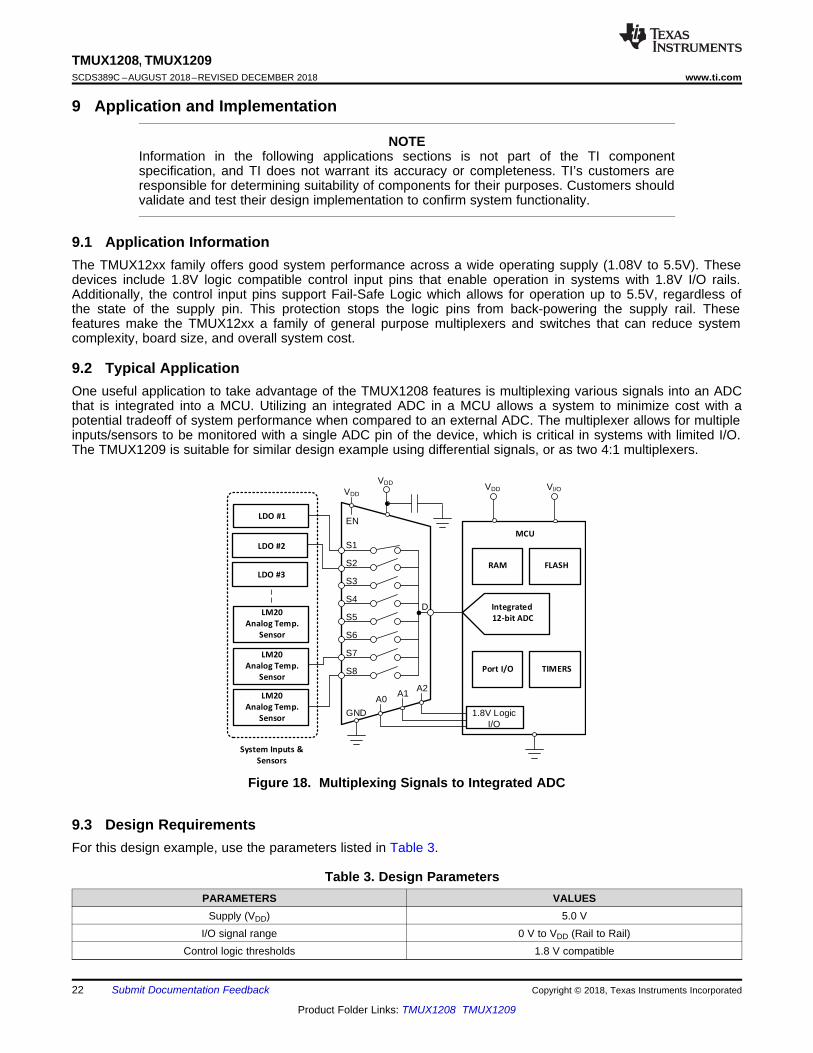
9.1 Application InformationThe TMUX12xx family offers good system performance across a wide operating supply (1.08V to 5.5V). Thesedevices include 1.8V logic compatible control input pins that enable operation in systems with 1.8V I/O rails.Additionally, the control input pins support Fail-Safe Logic which allows for operation up to 5.5V, regardless ofthe state of the supply pin. This protection stops the logic pins from back-powering the supply rail. Thesefeatures make the TMUX12xx a family of general purpose multiplexers and switches that can reduce systemcomplexity, board size, and overall system cost.
9.2 Typical ApplicationOne useful application to take advantage of the TMUX1208 features is multiplexing various signals into an ADCthat is integrated into a MCU. Utilizing an integrated ADC in a MCU allows a system to minimize cost with apotential tradeoff of system performance when compared to an external ADC. The multiplexer allows for multipleinputs/sensors to be monitored with a single ADC pin of the device, which is critical in systems with limited I/O.The TMUX1209 is suitable for similar design example using differential signals, or as two 4:1 multiplexers.
Figure 18. Multiplexing Signals to Integrated ADC
9.3 Design RequirementsFor this design example, use the parameters listed in Table 3.
Table 3. Design ParametersPARAMETERS VALUES
Supply (VDD) 5.0 VI/O signal range 0 V to VDD (Rail to Rail)
Control logic thresholds 1.8 V compatible

Source or Drain Voltage (V)
On
Res
ista
nce
(:)
0 0.5 1 1.5 2 2.5 3 3.5 4 4.5 50
20
40
60
80
VDD= 4.5VVDD= 3V
VDD= 1.62V
VDD= 1.08V
D001
23
TMUX1208, TMUX1209www.ti.com SCDS389C –AUGUST 2018–REVISED DECEMBER 2018
Product Folder Links: TMUX1208 TMUX1209
Submit Documentation FeedbackCopyright © 2018, Texas Instruments Incorporated
9.4 Detailed Design ProcedureThe TMUX1208 and TMUX1209 can be operated without any external components except for the supplydecoupling capacitors. If the parts desired power-up state is disabled, the enable pin should have a weak pull-down resistor and be controlled by the MCU via GPIO. All inputs being muxed to the ADC of the MCU must fallwithin the recommend operating conditions of the TMUX1208 and TMUX1209 including signal range andcontinuous current. For this design with a supply of 5 V the signal range can be 0 V to 5 V and the maxcontinuous current can be 30 mA.
9.5 Application Curve
TA = 25°C
Figure 19. On-Resistance vs Source or Drain Voltage
10 Power Supply Recommendations
The TMUX1208 and TMUX1209 operate across a wide supply range of 1.08 V to 5.5 V. Do not exceed theabsolute maximum ratings because stresses beyond the listed ratings can cause permanent damage to thedevices.
Power-supply bypassing improves noise margin and prevents switching noise propagation from the VDD supply toother components. Good power-supply decoupling is important to achieve optimum performance. For improvedsupply noise immunity, use a supply decoupling capacitor ranging from 0.1 μF to 10 μF from VDD to ground.Place the bypass capacitors as close to the power supply pins of the device as possible using low-impedanceconnections. TI recommends using multi-layer ceramic chip capacitors (MLCCs) that offer low equivalent seriesresistance (ESR) and inductance (ESL) characteristics for power-supply decoupling purposes. For very sensitivesystems, or for systems in harsh noise environments, avoiding the use of vias for connecting the capacitors tothe device pins may offer superior noise immunity. The use of multiple vias in parallel lowers the overallinductance and is beneficial for connections to ground planes.

A0
EN
N.C.
S1
S2
S3
A1
A2
GND
VDD
S5
S6
S4
Via to ground plane
TMUX1208
C
S8D
S7
Wide (low inductance) trace for powerVia to
ground plane
WORST BETTER BEST
1W min.
W
2W
24
TMUX1208, TMUX1209SCDS389C –AUGUST 2018–REVISED DECEMBER 2018 www.ti.com
Product Folder Links: TMUX1208 TMUX1209
Submit Documentation Feedback Copyright © 2018, Texas Instruments Incorporated
11 Layout
11.1 Layout Guidelines
11.1.1 Layout InformationWhen a PCB trace turns a corner at a 90° angle, a reflection can occur. A reflection occurs primarily because ofthe change of width of the trace. At the apex of the turn, the trace width increases to 1.414 times the width. Thisincrease upsets the transmission-line characteristics, especially the distributed capacitance and self–inductanceof the trace which results in the reflection. Not all PCB traces can be straight and therefore some traces mustturn corners. Figure 20 shows progressively better techniques of rounding corners. Only the last example (BEST)maintains constant trace width and minimizes reflections.
Figure 20. Trace Example
Route high-speed signals using a minimum of vias and corners which reduces signal reflections andimpedance changes. When a via must be used, increase the clearance size around it to minimize itscapacitance. Each via introduces discontinuities in the signal’s transmission line and increases the chance ofpicking up interference from the other layers of the board. Be careful when designing test points, through-hole pins are not recommended at high frequencies.
Figure 21 illustrates an example of a PCB layout with the TMUX1208. Some key considerations are:
• Decouple the VDD pin with a 0.1-µF capacitor, placed as close to the pin as possible. Make sure that thecapacitor voltage rating is sufficient for the VDD supply.
• Keep the input lines as short as possible.• Use a solid ground plane to help reduce electromagnetic interference (EMI) noise pickup.• Do not run sensitive analog traces in parallel with digital traces. Avoid crossing digital and analog traces if
possible, and only make perpendicular crossings when necessary.
11.2 Layout Example
Figure 21. TMUX1208 Layout Example

25
TMUX1208, TMUX1209www.ti.com SCDS389C –AUGUST 2018–REVISED DECEMBER 2018
Product Folder Links: TMUX1208 TMUX1209
Submit Documentation FeedbackCopyright © 2018, Texas Instruments Incorporated
12 Device and Documentation Support
12.1 Documentation Support
12.1.1 Related DocumentationTexas Instruments, Simplifying Design with 1.8 V logic Muxes and Switches.
Texas Instruments, QFN/SON PCB Attachment.
Texas Instruments, Quad Flatpack No-Lead Logic Packages.
12.2 Related LinksThe table below lists quick access links. Categories include technical documents, support and communityresources, tools and software, and quick access to order now.
Table 4. Related Links
PARTS PRODUCT FOLDER ORDER NOW TECHNICALDOCUMENTS
TOOLS &SOFTWARE
SUPPORT &COMMUNITY
TMUX1208 Click here Click here Click here Click here Click hereTMUX1209 Click here Click here Click here Click here Click here
12.3 Receiving Notification of Documentation UpdatesTo receive notification of documentation updates, navigate to the device product folder on ti.com. In the upperright corner, click on Alert me to register and receive a weekly digest of any product information that haschanged. For change details, review the revision history included in any revised document.
12.4 Community ResourcesThe following links connect to TI community resources. Linked contents are provided "AS IS" by the respectivecontributors. They do not constitute TI specifications and do not necessarily reflect TI's views; see TI's Terms ofUse.
TI E2E™ Online Community TI's Engineer-to-Engineer (E2E) Community. Created to foster collaborationamong engineers. At e2e.ti.com, you can ask questions, share knowledge, explore ideas and helpsolve problems with fellow engineers.
Design Support TI's Design Support Quickly find helpful E2E forums along with design support tools andcontact information for technical support.
12.5 TrademarksE2E is a trademark of Texas Instruments.
12.6 Electrostatic Discharge CautionThis integrated circuit can be damaged by ESD. Texas Instruments recommends that all integrated circuits be handled withappropriate precautions. Failure to observe proper handling and installation procedures can cause damage.
ESD damage can range from subtle performance degradation to complete device failure. Precision integrated circuits may be moresusceptible to damage because very small parametric changes could cause the device not to meet its published specifications.
12.7 GlossarySLYZ022 — TI Glossary.
This glossary lists and explains terms, acronyms, and definitions.
13 Mechanical, Packaging, and Orderable InformationThe following pages include mechanical, packaging, and orderable information. This information is the mostcurrent data available for the designated devices. This data is subject to change without notice and revision ofthis document. For browser-based versions of this data sheet, refer to the left-hand navigation.

PACKAGE OPTION ADDENDUM
www.ti.com 10-Dec-2020
Addendum-Page 1
PACKAGING INFORMATION
Orderable Device Status(1)
Package Type PackageDrawing
Pins PackageQty
Eco Plan(2)
Lead finish/Ball material
(6)
MSL Peak Temp(3)
Op Temp (°C) Device Marking(4/5)
Samples
TMUX1208PWR ACTIVE TSSOP PW 16 2000 RoHS & Green NIPDAU Level-1-260C-UNLIM -40 to 125 TM1208
TMUX1208RSVR ACTIVE UQFN RSV 16 3000 RoHS & Green NIPDAUAG Level-1-260C-UNLIM -40 to 125 1B4
TMUX1209PWR ACTIVE TSSOP PW 16 2000 RoHS & Green NIPDAU Level-1-260C-UNLIM -40 to 125 TM1209
TMUX1209RSVR ACTIVE UQFN RSV 16 3000 RoHS & Green NIPDAUAG Level-1-260C-UNLIM -40 to 125 1D2
(1) The marketing status values are defined as follows:ACTIVE: Product device recommended for new designs.LIFEBUY: TI has announced that the device will be discontinued, and a lifetime-buy period is in effect.NRND: Not recommended for new designs. Device is in production to support existing customers, but TI does not recommend using this part in a new design.PREVIEW: Device has been announced but is not in production. Samples may or may not be available.OBSOLETE: TI has discontinued the production of the device.
(2) RoHS: TI defines "RoHS" to mean semiconductor products that are compliant with the current EU RoHS requirements for all 10 RoHS substances, including the requirement that RoHS substancedo not exceed 0.1% by weight in homogeneous materials. Where designed to be soldered at high temperatures, "RoHS" products are suitable for use in specified lead-free processes. TI mayreference these types of products as "Pb-Free".RoHS Exempt: TI defines "RoHS Exempt" to mean products that contain lead but are compliant with EU RoHS pursuant to a specific EU RoHS exemption.Green: TI defines "Green" to mean the content of Chlorine (Cl) and Bromine (Br) based flame retardants meet JS709B low halogen requirements of <=1000ppm threshold. Antimony trioxide basedflame retardants must also meet the <=1000ppm threshold requirement.
(3) MSL, Peak Temp. - The Moisture Sensitivity Level rating according to the JEDEC industry standard classifications, and peak solder temperature.
(4) There may be additional marking, which relates to the logo, the lot trace code information, or the environmental category on the device.
(5) Multiple Device Markings will be inside parentheses. Only one Device Marking contained in parentheses and separated by a "~" will appear on a device. If a line is indented then it is a continuationof the previous line and the two combined represent the entire Device Marking for that device.
(6) Lead finish/Ball material - Orderable Devices may have multiple material finish options. Finish options are separated by a vertical ruled line. Lead finish/Ball material values may wrap to twolines if the finish value exceeds the maximum column width.
Important Information and Disclaimer:The information provided on this page represents TI's knowledge and belief as of the date that it is provided. TI bases its knowledge and belief on informationprovided by third parties, and makes no representation or warranty as to the accuracy of such information. Efforts are underway to better integrate information from third parties. TI has taken and

PACKAGE OPTION ADDENDUM
www.ti.com 10-Dec-2020
Addendum-Page 2
continues to take reasonable steps to provide representative and accurate information but may not have conducted destructive testing or chemical analysis on incoming materials and chemicals.TI and TI suppliers consider certain information to be proprietary, and thus CAS numbers and other limited information may not be available for release.
In no event shall TI's liability arising out of such information exceed the total purchase price of the TI part(s) at issue in this document sold by TI to Customer on an annual basis.
OTHER QUALIFIED VERSIONS OF TMUX1208 :
• Automotive: TMUX1208-Q1
NOTE: Qualified Version Definitions:
• Automotive - Q100 devices qualified for high-reliability automotive applications targeting zero defects
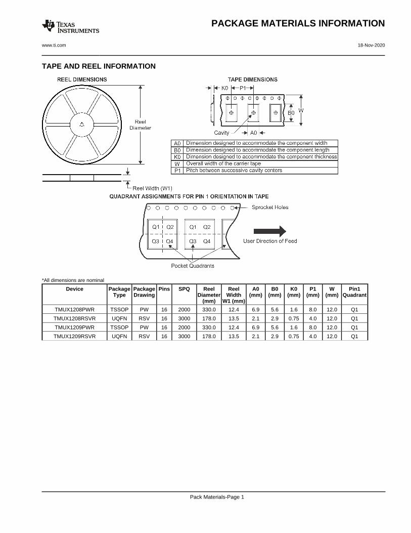
TAPE AND REEL INFORMATION
*All dimensions are nominal
Device PackageType
PackageDrawing
Pins SPQ ReelDiameter
(mm)
ReelWidth
W1 (mm)
A0(mm)
B0(mm)
K0(mm)
P1(mm)
W(mm)
Pin1Quadrant
TMUX1208PWR TSSOP PW 16 2000 330.0 12.4 6.9 5.6 1.6 8.0 12.0 Q1
TMUX1208RSVR UQFN RSV 16 3000 178.0 13.5 2.1 2.9 0.75 4.0 12.0 Q1
TMUX1209PWR TSSOP PW 16 2000 330.0 12.4 6.9 5.6 1.6 8.0 12.0 Q1
TMUX1209RSVR UQFN RSV 16 3000 178.0 13.5 2.1 2.9 0.75 4.0 12.0 Q1
PACKAGE MATERIALS INFORMATION
www.ti.com 18-Nov-2020
Pack Materials-Page 1

*All dimensions are nominal
Device Package Type Package Drawing Pins SPQ Length (mm) Width (mm) Height (mm)
TMUX1208PWR TSSOP PW 16 2000 853.0 449.0 35.0
TMUX1208RSVR UQFN RSV 16 3000 189.0 185.0 36.0
TMUX1209PWR TSSOP PW 16 2000 853.0 449.0 35.0
TMUX1209RSVR UQFN RSV 16 3000 189.0 185.0 36.0
PACKAGE MATERIALS INFORMATION
www.ti.com 18-Nov-2020
Pack Materials-Page 2
www.ti.com
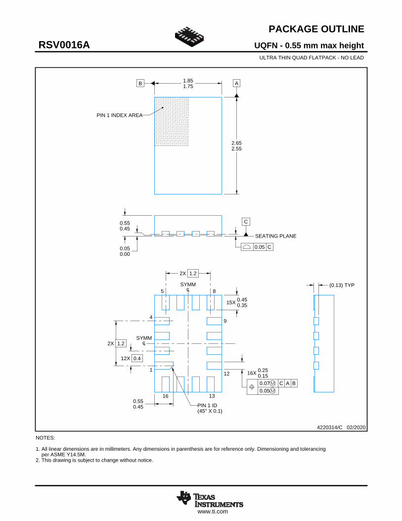
PACKAGE OUTLINE
C
1.851.75
2.652.55
0.550.45
0.050.00
2X 1.2
12X 0.4
2X 1.2
15X 0.450.35
16X 0.250.15
0.550.45
(0.13) TYP
UQFN - 0.55 mm max heightRSV0016AULTRA THIN QUAD FLATPACK - NO LEAD
4220314/C 02/2020
0.05 C
0.07 C A B0.05
NOTES: 1. All linear dimensions are in millimeters. Any dimensions in parenthesis are for reference only. Dimensioning and tolerancing per ASME Y14.5M. 2. This drawing is subject to change without notice.
PIN 1 INDEX AREA
SEATING PLANE
PIN 1 ID(45° X 0.1)
SYMM
SYMM
1
4
5 8
9
12
1316
SCALE 5.000
AB

www.ti.com
EXAMPLE BOARD LAYOUT
12X (0.4)
(R0.05) TYP
0.05 MAXALL AROUND
0.05 MINALL AROUND
15X (0.6)
16X (0.2)
(1.6)
(2.4)
(0.7)
UQFN - 0.55 mm max heightRSV0016AULTRA THIN QUAD FLATPACK - NO LEAD
4220314/C 02/2020
NOTES: (continued) 3. For more information, see Texas Instruments literature number SLUA271 (www.ti.com/lit/slua271).
SYMM
SYMM
LAND PATTERN EXAMPLEEXPOSED METAL SHOWN
SCALE: 25X
SEE SOLDER MASKDETAIL
1
4
5 8
9
12
1316
METAL EDGE
SOLDER MASKOPENING
EXPOSED METAL
METAL UNDERSOLDER MASK
SOLDER MASKOPENING
EXPOSEDMETAL
NON SOLDER MASKDEFINED
(PREFERRED)SOLDER MASK DEFINED
SOLDER MASK DETAILS

www.ti.com
EXAMPLE STENCIL DESIGN
15X (0.6)
16X (0.2)
12X (0.4)
(1.6)
(2.4)
(R0.05) TYP
(0.7)
UQFN - 0.55 mm max heightRSV0016AULTRA THIN QUAD FLATPACK - NO LEAD
4220314/C 02/2020
NOTES: (continued) 4. Laser cutting apertures with trapezoidal walls and rounded corners may offer better paste release. IPC-7525 may have alternate design recommendations.
SOLDER PASTE EXAMPLEBASED ON 0.125 MM THICK STENCIL
SCALE: 25X
SYMM
SYMM
1
4
5 8
9
12
1316

www.ti.com
PACKAGE OUTLINE
C
14X 0.65
2X4.55
16X 0.300.19
TYP6.66.2
1.2 MAX
0.150.05
0.25GAGE PLANE
-80
BNOTE 4
4.54.3
A
NOTE 3
5.14.9
0.750.50
(0.15) TYP
TSSOP - 1.2 mm max heightPW0016ASMALL OUTLINE PACKAGE
4220204/A 02/2017
1
89
16
0.1 C A B
PIN 1 INDEX AREA
SEE DETAIL A
0.1 C
NOTES: 1. All linear dimensions are in millimeters. Any dimensions in parenthesis are for reference only. Dimensioning and tolerancing per ASME Y14.5M. 2. This drawing is subject to change without notice. 3. This dimension does not include mold flash, protrusions, or gate burrs. Mold flash, protrusions, or gate burrs shall not exceed 0.15 mm per side. 4. This dimension does not include interlead flash. Interlead flash shall not exceed 0.25 mm per side.5. Reference JEDEC registration MO-153.
SEATINGPLANE
A 20DETAIL ATYPICAL
SCALE 2.500
www.ti.com
EXAMPLE BOARD LAYOUT
0.05 MAXALL AROUND
0.05 MINALL AROUND
16X (1.5)
16X (0.45)
14X (0.65)
(5.8)
(R0.05) TYP
TSSOP - 1.2 mm max heightPW0016ASMALL OUTLINE PACKAGE
4220204/A 02/2017
NOTES: (continued) 6. Publication IPC-7351 may have alternate designs. 7. Solder mask tolerances between and around signal pads can vary based on board fabrication site.
LAND PATTERN EXAMPLEEXPOSED METAL SHOWN
SCALE: 10X
SYMM
SYMM
1
8 9
16
15.000
METALSOLDER MASKOPENING
METAL UNDERSOLDER MASK
SOLDER MASKOPENING
EXPOSED METALEXPOSED METAL
SOLDER MASK DETAILS
NON-SOLDER MASKDEFINED
(PREFERRED)
SOLDER MASKDEFINED

www.ti.com
EXAMPLE STENCIL DESIGN
16X (1.5)
16X (0.45)
14X (0.65)
(5.8)
(R0.05) TYP
TSSOP - 1.2 mm max heightPW0016ASMALL OUTLINE PACKAGE
4220204/A 02/2017
NOTES: (continued) 8. Laser cutting apertures with trapezoidal walls and rounded corners may offer better paste release. IPC-7525 may have alternate design recommendations. 9. Board assembly site may have different recommendations for stencil design.
SOLDER PASTE EXAMPLEBASED ON 0.125 mm THICK STENCIL
SCALE: 10X
SYMM
SYMM
1
8 9
16

IMPORTANT NOTICE AND DISCLAIMER
TI PROVIDES TECHNICAL AND RELIABILITY DATA (INCLUDING DATASHEETS), DESIGN RESOURCES (INCLUDING REFERENCE DESIGNS), APPLICATION OR OTHER DESIGN ADVICE, WEB TOOLS, SAFETY INFORMATION, AND OTHER RESOURCES “AS IS” AND WITH ALL FAULTS, AND DISCLAIMS ALL WARRANTIES, EXPRESS AND IMPLIED, INCLUDING WITHOUT LIMITATION ANY IMPLIED WARRANTIES OF MERCHANTABILITY, FITNESS FOR A PARTICULAR PURPOSE OR NON-INFRINGEMENT OF THIRD PARTY INTELLECTUAL PROPERTY RIGHTS.These resources are intended for skilled developers designing with TI products. You are solely responsible for (1) selecting the appropriate TI products for your application, (2) designing, validating and testing your application, and (3) ensuring your application meets applicable standards, and any other safety, security, or other requirements. These resources are subject to change without notice. TI grants you permission to use these resources only for development of an application that uses the TI products described in the resource. Other reproduction and display of these resources is prohibited. No license is granted to any other TI intellectual property right or to any third party intellectual property right. TI disclaims responsibility for, and you will fully indemnify TI and its representatives against, any claims, damages, costs, losses, and liabilities arising out of your use of these resources.TI’s products are provided subject to TI’s Terms of Sale (www.ti.com/legal/termsofsale.html) or other applicable terms available either on ti.com or provided in conjunction with such TI products. TI’s provision of these resources does not expand or otherwise alter TI’s applicable warranties or warranty disclaimers for TI products.
Mailing Address: Texas Instruments, Post Office Box 655303, Dallas, Texas 75265Copyright © 2020, Texas Instruments Incorporated