Embed Size (px)
Citation preview
TNA ENERGY 2011

TNA
TNA
TNA
TNA Energy
Energy
Energy
Energy 2011
2011
2011
2011
ImagineNano April 11-14, 2011
INDEX: INVITED CONTRIBUTIONS
pag
Michaël Grätzel (EPFL, Switzerland) "The advent of mesosocopic solar cells"
505
Antonio Luque (Univ Politécnica de Madrid, Spain) "Nanotechnology for more efficient photovoltaics: the quantum dot intermediate band solar cell"
513
Emilio Mendez (Brookhaven National Laboratory, USA) "Nanotechnology for the Energy Challenge"
-
INDEX: INVITED CONTRIBUTIONS (OMNT SESSION)
pag
Kazuhito Kinosita (Waseda Univ., Japan) "A rotary molecular motor with amazing performance"
-
Ana Moore (Arizona Univ., USA) "Design of Photoelectrochemical Cells for the Splitting of Water and Production of Fuel"
521
Nicolas Tetreault (EPFL, Switzerland) "Title not available"
-
INDEX: KEYNOTE CONTRIBUTIONS
pag
Juan Bisquert (Universitat Jaume I, Spain ) "Dynamics and distribution of photogenerated carriers in organic solar cells and in dye solar cells"
489
Fernando Briones (IMM-CNM-CSIC, Spain) "Molecular Beam Epitaxy (MBE), a versatile tool to integrate model semiconductor nanostructures into advanced solar cell concepts"
491
Alejandro A. Franco (CEA-LITEN, France) "Title not available"
-
David Fuertes Marron (UPM, Spain) "Chalcopyrite-based nanostructures: new prospects for highly efficient photovoltaic devices"
499
Jordi Martorell (ICFO, Spain) "New routes for the fabrication of Organic Photovoltaic Cells"
519
Xavier Obradors (ICMAB-CSIC, Spain) "Chemical solution approaches to self-assembled and nanocomposite superconducting and ferromagnetic films"
523
Taro Toyoda (The Univ of Electro-Communications, Japan) "Characterization of Optical Properties of Semiconductor Quantum Dot-Sensitized Solar Cells together with Ultrafast Carrier Dynamic Propertie"
527
INDEX: KEYNOTE CONTRIBUTIONS (OMNT SESSION)
pag
Franck Artzner (CNRS – IPR, France) "Bio-inspired scaffolds to manufacture nanomaterials :nanotubes & Quantum Dots arrays"
487
Frédéric Favier (CNRS – ICG, France) "Title not available"
-
Christophe Lethien (CNRS – IEMN, France) "Silicon nanowires and nanopillars arrays for lithium-ion battery and micro-battery: overview, challenges and perspectives"
511
Pere Roca i Cabarrocas (CNRS – LPICM, France) "Title not available"
-

TNA Energy
TNA Energy
TNA Energy
TNA Energy 2011
2011
2011
2011
ImagineNano April 11-14, 2011
INDEX: ORAL CONTRIBUTIONS
pag
Roger Amade Rovira (Universitat de Barcelona, Spain) "Carbon nanotubes lined by anodic deposition of MnO2 for supercapacitor application"
485
Annalisa Bruno (Imperial College London, United Kingdom) "Exciton diffusion Length and morphology TFB/ fullerene blends"
493
José C. Conesa (Instituto de Catálisis y Petroleoquímica, CSIC, Spain) "Intermediate band materials for more efficient solar energy use: quantum modeling and experimental realizations"
495
Anderson Dias (Universidade Federal de Ouro Preto, Brazil) "Microwave synthesis and Raman scattering of nanostructured lanthanide-doped NaTaO3 thermoelectric materials"
497
Arnaldo Galbiati (Solaris Photonics, United Kingdom) "A Novel Ultra Thin Film Photovoltaic Technology with Alkali Metal Active Region"
501
Marcin Gorzny (CIC nanoGUNE, Spain) "Synthesis of High-Surface-Area Platinum Nanotubes Using a Viral Template"
503
Ladislav Kavan (J Heyrovsky Institute of Physical Chemistry, Czech Republic) "Optically Transparent Cathode for Dye Sensitized Solar Cells Based on Graphene Nanoplatelets"
507
Elin Larsson (Applied Physics, Sweden) "Indirect Nanoplasmonic Sensing in Catalysis: Sintering, Reactant Surface Coverage Changes and Optical Nanocalorimetry"
509
Enrique Macia (UCM, Spain) "Optimizing the thermoelectric figure of merit of aperiodic solids"
515
Marisol Martin-Gonzalez (IMM-CSIC, Spain) "Nanoengineering Thermoelectrics for Energy Harvesting."
517
Xavier Oriols (Universitat Autònoma de Barcelona, Spain) "Towards Power Optimization in Nanoscale Systems through the use of Many-electron Correlations"
525

TNA Energy
TNA Energy
TNA Energy
TNA Energy 2011
2011
2011
2011
ImagineNano April 11-14, 2011
ALPHABETICAL ORDER
I: Invited / IM: Invited OMNT Session / K: Keynote / KM: Keynote OMNT Session / O: Oral
pag
Roger Amade Rovira (Universitat de Barcelona, Spain) "Carbon nanotubes lined by anodic deposition of MnO2 for supercapacitor application"
O 485
Franck Artzner (CNRS – IPR, France) "Bio-inspired scaffolds to manufacture nanomaterials :nanotubes & Quantum Dots arrays"
KM 487
Juan Bisquert (Universitat Jaume I, Spain ) "Dynamics and distribution of photogenerated carriers in organic solar cells and in dye solar cells"
K 489
Fernando Briones (IMM-CNM-CSIC, Spain) "Molecular Beam Epitaxy (MBE), a versatile tool to integrate model semiconductor nanostructures into advanced solar cell concepts"
K 491
Annalisa Bruno (Imperial College London, United Kingdom) "Exciton diffusion Length and morphology TFB/ fullerene blends"
O 493
José C. Conesa (Instituto de Catálisis y Petroleoquímica, CSIC, Spain) "Intermediate band materials for more efficient solar energy use: quantum modeling and experimental realizations"
O 495
Anderson Dias (Universidade Federal de Ouro Preto, Brazil) "Microwave synthesis and Raman scattering of nanostructured lanthanide-doped NaTaO3 thermoelectric materials"
O 497
Frédéric Favier (CNRS – ICG, France) "Title not available"
KM -
Alejandro A. Franco (CEA-LITEN, France) "Title not available"
K -
David Fuertes Marron (UPM, Spain) "Chalcopyrite-based nanostructures: new prospects for highly efficient photovoltaic devices"
K 499
Arnaldo Galbiati (Solaris Photonics, United Kingdom) "A Novel Ultra Thin Film Photovoltaic Technology with Alkali Metal Active Region"
O 501
Marcin Gorzny (CIC nanoGUNE, Spain) "Synthesis of High-Surface-Area Platinum Nanotubes Using a Viral Template"
O 503
Michaël Grätzel (EPFL, Switzerland) "The advent of mesosocopic solar cells"
I 505
Ladislav Kavan (J Heyrovsky Institute of Physical Chemistry, Czech Republic) "Optically Transparent Cathode for Dye Sensitized Solar Cells Based on Graphene Nanoplatelets"
O 507
Kazuhito Kinosita (Waseda Univ., Japan) "A rotary molecular motor with amazing performance"
IM -
Elin Larsson (Applied Physics, Sweden) "Indirect Nanoplasmonic Sensing in Catalysis: Sintering, Reactant Surface Coverage Changes and Optical Nanocalorimetry"
O 509
Christophe Lethien (CNRS – IEMN, France) "Silicon nanowires and nanopillars arrays for lithium-ion battery and micro-battery: overview, challenges and perspectives"
KM 511
Antonio Luque (Univ Politécnica de Madrid, Spain) "Nanotechnology for more efficient photovoltaics: the quantum dot intermediate band solar cell"
I 513
Enrique Macia (UCM, Spain) "Optimizing the thermoelectric figure of merit of aperiodic solids"
O 515
Marisol Martin-Gonzalez (IMM-CSIC, Spain) "Nanoengineering Thermoelectrics for Energy Harvesting."
O 517
Jordi Martorell (ICFO, Spain) "New routes for the fabrication of Organic Photovoltaic Cells"
K 519
Emilio Mendez (Brookhaven National Laboratory, USA) "Nanotechnology for the Energy Challenge"
I -

TNA Energ
TNA Energ
TNA Energ
TNA Energyy yy 2011
2011
2011
2011
ImagineNano April 11-14, 2011
I: Invited / IM: Invited OMNT Session / K: Keynote / KM: Keynote OMNT Session / O: Oral
pag
Ana Moore (Arizona Univ., USA) "Design of Photoelectrochemical Cells for the Splitting of Water and Production of Fuel"
IM 521
Xavier Obradors (ICMAB-CSIC, Spain) "Chemical solution approaches to self-assembled and nanocomposite superconducting and ferromagnetic films"
K 523
Xavier Oriols (Universitat Autònoma de Barcelona, Spain) "Towards Power Optimization in Nanoscale Systems through the use of Many-electron Correlations"
O 525
Pere Roca i Cabarrocas (CNRS – LPICM, France) "Title not available"
KM -
Nicolas Tetreault (EPFL, Switzerland) "Title not available"
IM -
Taro Toyoda (The Univ of Electro-Communications, Japan) "Characterization of Optical Properties of Semiconductor Quantum Dot-Sensitized Solar Cells together with Ultrafast Carrier Dynamic Propertie"
K 527

ABSTRACTS
ALPHABETICAL ORDER
TNA ENERGY 2011

TNA
TNA
TNA
TNA Energy
Energy
Energy
Energy 2011
2011
2011
2011
ImagineNano April 11-14, 2011
485
CARBON NANOTUBES LINED BY ANODIC DEPOSITION OF MNO2 FOR SUPERCAPACITOR
APPLICATION
Roger Amade, Eric Jover, Shahzad Hussein and Enric Bertran
Department of Applied Physics and Optics, FEMAN Group, Universitat de Barcelona, c/ Martí i Franquès 1, 08028 Barcelona, Spain
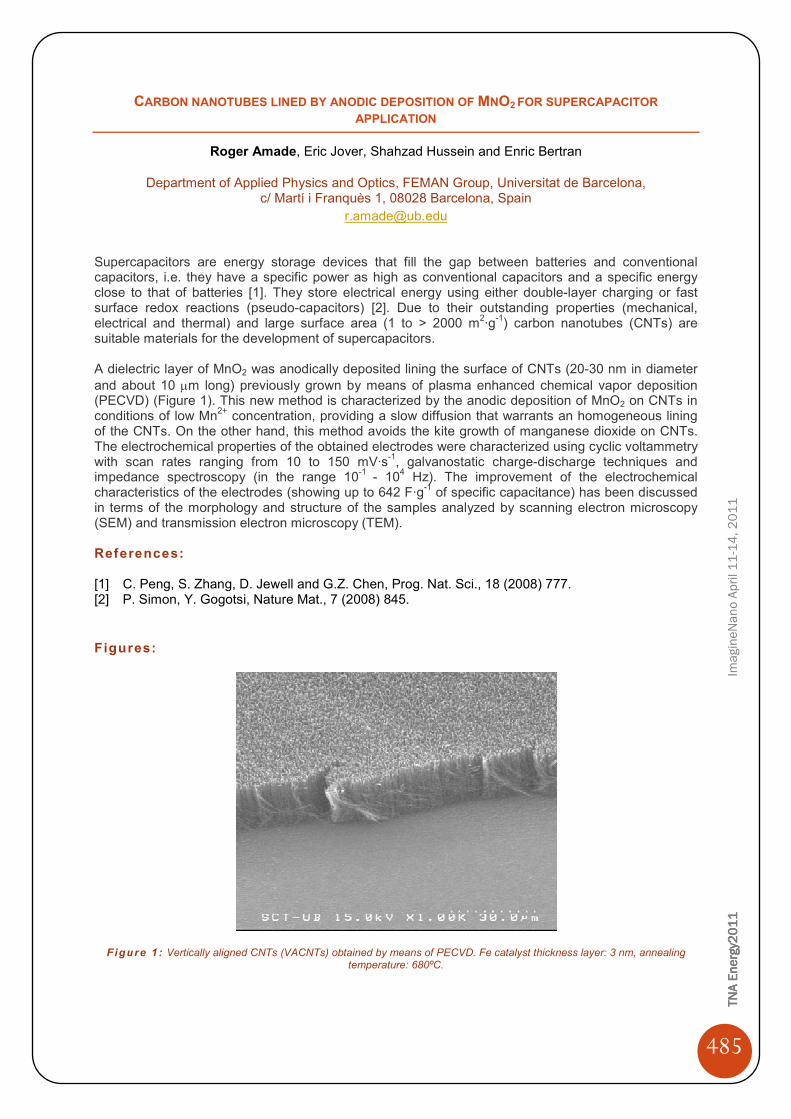
Supercapacitors are energy storage devices that fill the gap between batteries and conventional capacitors, i.e. they have a specific power as high as conventional capacitors and a specific energy close to that of batteries [1]. They store electrical energy using either double-layer charging or fast surface redox reactions (pseudo-capacitors) [2]. Due to their outstanding properties (mechanical, electrical and thermal) and large surface area (1 to > 2000 m2·g-1) carbon nanotubes (CNTs) are suitable materials for the development of supercapacitors. A dielectric layer of MnO2 was anodically deposited lining the surface of CNTs (20-30 nm in diameter and about 10 µm long) previously grown by means of plasma enhanced chemical vapor deposition (PECVD) (Figure 1). This new method is characterized by the anodic deposition of MnO2 on CNTs in conditions of low Mn2+ concentration, providing a slow diffusion that warrants an homogeneous lining of the CNTs. On the other hand, this method avoids the kite growth of manganese dioxide on CNTs. The electrochemical properties of the obtained electrodes were characterized using cyclic voltammetry with scan rates ranging from 10 to 150 mV·s-1, galvanostatic charge-discharge techniques and impedance spectroscopy (in the range 10-1 - 104 Hz). The improvement of the electrochemical characteristics of the electrodes (showing up to 642 F·g-1 of specific capacitance) has been discussed in terms of the morphology and structure of the samples analyzed by scanning electron microscopy (SEM) and transmission electron microscopy (TEM).
References: [1] C. Peng, S. Zhang, D. Jewell and G.Z. Chen, Prog. Nat. Sci., 18 (2008) 777. [2] P. Simon, Y. Gogotsi, Nature Mat., 7 (2008) 845. Figures:
Figure 1 : Vertically aligned CNTs (VACNTs) obtained by means of PECVD. Fe catalyst thickness layer: 3 nm, annealing
temperature: 680ºC.

TNA
TNA
TNA
TNA Energy
Energy
Energy
Energy 2011
2011
2011
2011
ImagineNano April 11-14, 2011
486
TNA
TNA
TNA
TNA Energy
Energy
Energy
Energy 2011
2011
2011
2011
ImagineNano April 11-14, 2011
487
BIO-INSPIRED SCAFFOLDS TO MANUFACTURE NANOMATERIALS: NANOTUBES & QUANTUM DOTS ARRAYS
Franck Artzner
Biomimetic Self-Assemblies – UMR 6251 CNRS- Université Rennes1, France [email protected]
Nature is an unlimited source of inspiration for the development of materials presenting original optical properties. The current structural knowledge of some of these biological assemblies is promising as an inspiration source to try to mimics their supramolecular organizations. The development of simplified system presenting properties close to biological assemblies is of great interest. To this end, there is still a long way in order to understand not only the structures, but also their formation mechanisms. Lanreotide molecules self-assemble in water into highly monodisperse supramolecular nanotubes, the diameter and wall thickness of which are 244Å and 18Å respectively. [1] Following biomineralization principles, we show that the self-assembled nanotubes can be used as a template to produce micron-long, bilayered silica nanotubes having a monodisperse diameter of 29 nm. The nanotubes organize spontaneously into centimeter-size, highly ordered bundles. Furthermore, the formation mechanism was elucidated using a range of techniques, including X ray diffraction, optical and electron microscopy [2]. Lamellar hybrid condensed phase in which the QDs are densely packed in the plane of the layers can be prepared [3]. The 3D crystallization of the QDs can be achieved by the addition of actin proteins that polymerize into filaments with well defined pitch and diameter. New photophysical properties will be presented. These examples of bio-inspired technologies demonstrate the possibility of solving the challenge of efficiency, less expensive and environmental technologies. References: [1] Biomimetic organization : octapeptide self assembly into nanotubes of viral capsid like dimension
C. Valéry, M. Paternostre, B.Robert, T. Gulik-Krzywicki, T. Narayanan, J.-C. Dedieu, G. Keller, M.-L. Torres, R. Cherif-Cheikh, P. Calvo & F. Artzner Proc. Natl. Acad. Sci. USA, 2003,100(18), 10258-10262.
[2] Hierarchical architectures by synergy between dynamical template self-assembly and biomineralization, E. Pouget, E. Dujardin, A. Cavalier, A. Moreac, C. Valéry, V. Marchi-Artzner, T. Weiss, A. Renault, M. Paternostre, F. Artzner Nature Materials, 2007, 6, 434-439.
[3] Interaction between water-soluble peptidic CdSe/ZnS nanocrystals and vesicles: formation of hybrid vesicles and condensed lamellar phases, A. Dif, E. Henry, F. Artzner, M. Baudy-Floc h, M. Schmutz, M. Dahan, V. Marchi-Artzner, J. Am. Chem. Soc., 2008, 130(26), 8289-8296.

TNA
TNA
TNA
TNA Energy
Energy
Energy
Energy 2011
2011
2011
2011
ImagineNano April 11-14, 2011
488

TNA
TNA
TNA
TNA Energy
Energy
Energy
Energy 2011
2011
2011
2011
ImagineNano April 11-14, 2011
489
DYNAMICS AND DISTRIBUTION OF PHOTOGENERATED CARRIERS IN ORGANIC SOLAR CELLS AND IN
DYE SOLAR CELLS
Juan Bisquert
Grup de Dispositius Fotovoltaics I Optoelectrònics, Dep. de Física, Avda Sos Baynat sn, 12071 Castelló, Spain
Based on large experience on DSC characterization by Impedance Spectroscopy (IS), we are now interested to provide detailed understanding of the factors determining the cell performance.[1] I discuss here the relation between recombination resistance and capacitance of the cell measured by IS, with the j-V curve both in the dark and under (1 sun) illumination. The most challenging aspect of the analysis is to separate the change of conduction band position from an array of charge transfer kinetics factors. This is not trivial since surface changes induced by the presence of the dye may affect both the beta parameter that modifies the fill factor, and slow the charge transfer kinetics, by surface blocking or other factors. We can provide a detailed energetic map that allows to explore innovations such as the new redox couple with more positive potential, or alternative nanostructure. Similar methods can be applied in quantum dot sensitized solar cell to speed up the progress oh these cells that is developing strongly in the last few years.[2] In organic solar cells, it is important to obtain a picture of the carrier distribution, first in the dark, when the system is in equilibrium, and then at progressive illumination, and as a function of the potential.[3] We discuss our views on this which is obtained from measurement, specifically by scanning the capacitance over a broad set of conditions. This has been done in the standard PCM/P3HT configuration, some important informations about the carrier distribution can be obtained, and implications for open-circuit voltage are discussed. References: [1] Fabregat-Santiago, F.; Garcia-Belmonte, G.; Mora-Seró, I.; Bisquert, J. "Impedance spectroscopy
of hybrid and organic solar cells". Physical Chemistry Chemical Physics 2011, 10.1039/C1030CP02249G
[2] Gónzalez-Pedro, V.; Xu, X.; Mora-Seró, I.; Bisquert , J. "Modeling High-Efficiency Quantum Dot Sensitized Solar Cells". ACS Nano 2010, 4, 5783–5790
[3] Boix, P. P.; Ajuria, J.; Etxebarria, I.; Pacios, R.; Garcia-Belmonte, G.; Bisquert, J. "Role of ZnO Electron-Selective Layers in Regular and Inverted Bulk Heterojunction Solar Cells". Journal of Physical Chemistry Letters 2011, 2, 407–411
Figures:
Figure 1: Energetocs of dye solar cells with different types of dyes.

TNA
TNA
TNA
TNA Energy
Energy
Energy
Energy 2011
2011
2011
2011
ImagineNano April 11-14, 2011
490

TNA
TNA
TNA
TNA Energy
Energy
Energy
Energy 2011
2011
2011
2011
ImagineNano April 11-14, 2011
491
MOLECULAR BEAM EPITAXY (MBE), A VERSATILE TOOL TO INTEGRATE MODEL SEMICONDUCTOR
NANOSTRUCTURES INTO ADVANCED SOLAR CELL CONCEPTS
F.Briones, J. M. Ripalda, D. Alonso-Álvarez, B. Alén, J. M. Llorens, A. G. Taboada, M. L. Dotor, Y. González
IMM-Instituto de Microelectrónica de Madrid (CNM-CSIC), Isaac Newton 8, 28760 Tres Cantos, Spain
Semiconductor quantum nanostructures are at the base of advanced designs for high efficiency photovoltaic solar cells. MBE technology is an advanced and versatile technique to create highly perfect single-crystalline semiconductor heterostructures with superb control of dimensions, composition and doping in the nanoscale. In particular, this technique is perfectly adequate to epitaxialy grow complete device structures containing tailor designed nanostructures, due to its compatibility with a variety of in-situ control and characterization techniques. We will describe how MBE is applied at IMM to create model solar cell structures incorporating self-assembled Quantum Dots stacks and Quantum Posts in the InAs/GaAs or InAs/InP systems, together with sharp tunnel junctions, that should allow to test ideas, to study physics of novel structures and to obtain realistic estimations on the feasibility of advanced designs for high efficiency solar cells as the IB concept [1] After a brief introduction on the peculiarities and applications of MBE, a more detailed description will be given of the principles and techniques used to design, monitor and control the strain distribution, accumulation and compensation. Examples will be presented of cells containing heterostructures and materials with large lattice parameter mismatch and corresponding large local strains. The incorporation of Phosphorus or Antimony as strain creating or compensating elements results in interesting device properties [2]. As a particular case of extreme difficulty, the fabrication of GaAs solar cells, with a large number of stacked QDs layers in the intrinsic zone to enhance QD absorption characteristics without generating dislocations, will be considered. [3] As a further example, the techniques to grow a new type of nanostructures, Quantum Posts, will be considered. Main interest of using quantum posts instead of quantum dots to form the intermediate band is intimately related with their elongated shape, and hence their potential to tailor the absorption of the photons that cause transitions from the IB to the CB. Typical QDs grown in the Stranski-Krastanov mode have a flat shape with the vertical dimension shorter than the lateral ones. Producing QDs with increased vertical dimension can increase the transition element related to IB to CB transitions and therefore increase the absorption associated to this transition. Stacking several QDs (that is, creating a QP) can be a way to produce the desired aspect ratio. On the other hand, it is of interest to research on the non delta-like density of states introduced by the QPs to investigate the limits in which the extra density of states introduced does not jeopardize the voltage preservation predicted for the IBSC. Quantum posts are assembled by epitaxial growth of closely spaced quantum dot layers, modulating the composition of a semiconductor alloy, typically InGaAs. In contrast with most self-assembled nanostructures, the height of quantum posts can be controlled with nanometer precision, up to a maximum value limited by the accumulated stress due to the lattice mismatch. Here we present a strain compensation technique based on the controlled incorporation of phosphorous, which substantially increases the maximum attainable quantum post height. The luminescence from the resulting nanostructures presents giant linear polarization anisotropy. Finally, novel process techniques, derived from the understanding of MBE growth kinetics in the research environment, but applicable to other materials and polycrystalline thin film structures, will be discussed in view of their application to solar cell commercial fabrication. We conclude that in the next future, similarly to what has been happening in the microelectronics field, a remarkable photovoltaic cell sophistication and efficiency will be compatible with a large scale, low cost industrial scenario.
TNA
TNA
TNA
TNA Energy
Energy
Energy
Energy 2011
2011
2011
2011
ImagineNano April 11-14, 2011
492
References: [1] A. Luque and A. Marti, Phys. Rev. Lett. 78, (1997) 5014 [2] Diego Alonso-Álvarez, Benito Alén, Jorge M. García, J. M. Ripalda, Appl. Phys. Lett. 91, (2007)
263103 [3] D. Alonso-Álvarez, A. G. Taboada, J. M. Ripalda, B. Alén, Y. González, L. González, J. M.
García, F. Briones, Appl. Phys. Lett. 93, (2008)123114 Figures:
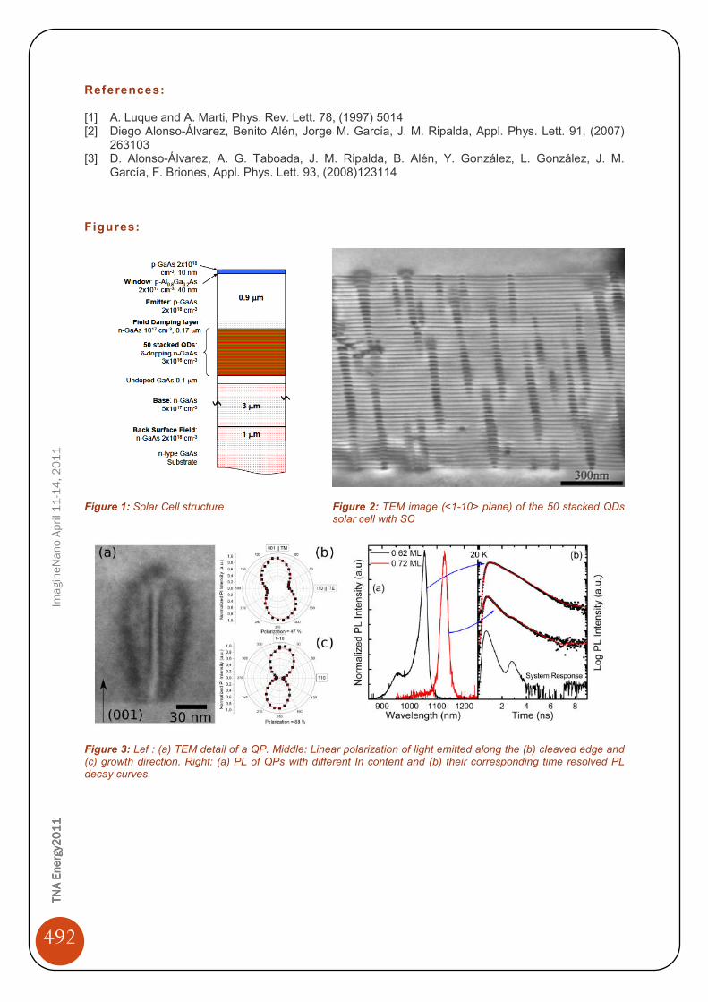
Figure 1: Solar Cell structure Figure 2: TEM image (<1-10> plane) of the 50 stacked QDs
solar cell with SC
Figure 3: Lef : (a) TEM detail of a QP. Middle: Linear polarization of light emitted along the (b) cleaved edge and (c) growth direction. Right: (a) PL of QPs with different In content and (b) their corresponding time resolved PL decay curves.

TNA
TNA
TNA
TNA Energy
Energy
Energy
Energy 2011
2011
2011
2011
ImagineNano April 11-14, 2011
493
EXCITON DIFFUSION LENGTH AND MORPHOLOGY IN TFB/ FULLERENE BLENDS
Annalisa Bruno1, Luke Reynolds1, Clare Dyer-Smith2, Jenny Nelson2, Saif Haque1
1Department of Chemistry, Imperial College London, London, United Kingdom; 2Department of Physics, Imperial College London, London, United Kingdom
[email protected] Organic materials present a promising direction for potentially cheaper solar cells and to allow the construction of mechanically flexible cells. Although recent bulk-heterojunction devices have given really encouraging performances, reaching efficiencies around 8% [1], more work is needed in order to be able to understand the energy losses within these devices, and so increase their efficiency. As many recent studies have outlined, the excited state dynamics and the processes occurring at the donor-acceptor (D/A) interface [2-4] are critical to the performance of solar cells. The efficiency of charge separation at the D/A interface is crucial to the photocurrent generation in organic solar cells, and a complete understanding of this process is essential in order to be able to maximize the power generation efficiency. In fact in a polymer-based photovoltaic device light absorption by the polymer usually results predominantly in formation of excitons that diffuse through the polymer layer to reach the interface with the electron acceptor, there they can dissociates into a electrostatically bound charge pair. The pair then separates into a positive polaron in the donor and a negative polaron in the acceptor, which are then transported to the respective electrodes. [5,6]. Here we present a recent work performed using a fluorescence up-conversion technique to systematically study the effect of using three different types of acceptors as [6,6]-phenyl-C61 butyric acid methyl ester (mono-PCBM) and its multi-adduct analogues bis-PCBM and tris-PCBM on the emission quenching and morphology in [9,9-dioctylfluorene-co-N-(4-butylphenyl)-diphenylamine] (TFB) blends. All molecular structures are reported in figure 1. The innovative experimental set up allows us to probe the ultrafast (<1 ps) excited state dynamics of photo-generated species with a high resolution (<200 fs). This means that we are able to follow the formation of the excited state in the polymer and the charge separation process at the interface with the acceptor. The ultrafast fluorescence quenching for the three different acceptors has been correlate with the different blends morphologies. Moreover a new excitons dynamic model has been developed to reproduce the experimental quenching rates and in order to evaluate their diffusion length, for the first time from the ultrafast fluorescence measurements. We also present independent measurements of diffusion length to support our evaluation. When coupled with other standard spectroscopic techniques the exciton recombination dynamics of such systems allow quantitative design rules to be formalized which is essential for the continued development of highly efficient organic bulk hetero-junction PV devices. References: [1] Y Liang, Z. Xu, J. Xia, S. Tsai, Y. Wu, G.Li, C. Ray, L. Yu, Advanced Materials 22 (2010) 2696 [2] J.J.Benson-Smith, H. Ohkita, S. Cook, J.R. Durrant, D.D.C. Bradley, J.Nelson, Dalton
Transactions, 2009 (2009)10000. [3] D Veldman, S.C.J. Meskers, R.A.J. Janssen, Advanced Functional Materials 19 (2009) 1 [4] M.A. Faist, P.E. Keivanidis, S. Foster, P.H. Wöbkenberg, T.D. Anthopoulos, D.D.C. Bradley, J.
Durrant, J. Nelson, Journal of Polymer Science Part B: Polymer Physics 49 (2010) 45 [5] V, Mihailetchi, L. J. A Koster, J. C. Hummelen, P.W.M. Blom, Physical Review Letters 93 (2004)
216601. [6] E. Hendry, J.M. Schins, L.P. Candeias, L.D.A. Siebbeles, M. Bonn, Physical Review Letters 92
(2004) 196601.

TNA
TNA
TNA
TNA Energy
Energy
Energy
Energy 2011
2011
2011
2011
ImagineNano April 11-14, 2011
494
Figures:
Figure 1 : TFB molecular structure and energy levels are reported in the upper part. MonoPCBM, bisPCBM, and trisPCBM
molecular structures are in the lower part.
TNA
TNA
TNA
TNA Energy
Energy
Energy
Energy 2011
2011
2011
2011
ImagineNano April 11-14, 2011
495
INTERMEDIATE BAND MATERIALS FOR MORE EFFICIENT SOLAR ENERGY USE: QUANTUM MODELING
AND EXPERIMENTAL REALIZATIONS
J. C. Conesa, P. Wahnón, R. Lucena, P. Palacios, I. Aguilera, F. Fresno, Y. Seminovski
*Instituto de Catálisis y Petroleoquímica, CSIC, Marie Curie 2, 28049 Madrid, Spain #Instituto de Energía Solar, Univ. Politécnica de Madrid, Ciudad Universitaria s/n, Madrid, Spain
The intermediate band (IB) solar cell (Fig. 1) has been proposed [1] to increase photovoltaic efficiency by a factor above 1.5, based on the absorption of two sub-bandgap photons to promote an electron across the bandgap. To realize this principle, that can be applied also to obtain efficient photocatalysis with sunlight, we proposed in recent years several materials where a metal or heavy element, substituting for an electropositive atom in a known semiconductor that has an appropriate band gap width (around 2 eV), forms inside the gap the partially filled levels needed for this aim. After studying Ga(As,P) with Ga partially substituted by Ti or Cr [2], we proposed several systems that could be made in thin film form: a) Ti- or Cr- substituted CuGaS2 or similar chalcopyrite (Fig. 2), where the thermodynamics of formation is seen to be less disfavourable than e.g. insertion of Mn in GaAs [3]; b) In2S3 and other sulphides containing octahedral In, which when doped with Ti or V form also the IB according to quantum calculations [4] (Fig. 3). The V-doped In2S3 material is particularly promising. Being based on a binary compound host, controlling its stoichiometry should be easy. In addition In2S3, with Eg= 2.0 eV, is used as buffer layer in thin film CIGS PV cells, so that the known technology to make it in thin film form could be used. Besides, we have synthesized it in nanocrystalline form [5] and shown that its optical absorption spectrum has the features predicted by quantum calculations for the IB structure (Fig. 4). Furthermore, recent photocatalytic tests made with it [6] show that the V dopant extends its spectral response down to the IR range without increasing recombination, which would decrease its efficiency. c) Octahedral SnIV sulphide and other similar compounds show also, according to DFT modeling (Fig. 5), the formation of an IB with the desired characteristics when V, Nb or similar metals are introduced at Sn sites [7]. The experimental synthesis of such sulphide is in progress, and first results obtained show optical absorption spectra matching again the expectations for an IB material (Fig. 6). d) Another class of IB materials consists of Si heavily doped with certain elements. With Ti as dopant the desired IB electronic structure appears (Fig. 7) if Ti lies at interstitial sites [8]. Such material has been prepared by ion implantation methods, and its electrical properties [9] show uncommon features that can be explained assuming the formation of a partially filled band a few tenths of eV below the conduction band, as predicted by the DFT calculations. Although its band gap is not optimum to get high efficiency, it can serve as benchmark to study the behaviour of IB materials in single-crystal form. We could also show that substitution of Si by S or Se, accompanied by hole doping, provides an IB material as well [10]. e) Finally we showed with DFT calculations that a clathrate-type silicon polymorph, that in pure form has Eg=1.9 eV and for which some thin film preparation recipes exist, forms an IB material when a metal as Ag is occluded in its cavities or some of its Si atoms are substitued by a transition metal as V [11] (Fig. 8). References: [1] Luque and A. Martí, Phys. Rev. Lett. 78 (1997) 5014 [2] P. Palacios et al. Phys. Rev. B 73 (2006) 085206; ibid. J. Chem. Phys. 124 (2006) 014711 [3] P. Palacios et al. Thin Solid Films 515 (2007) 6280; ibid. J. Phys. Chem. C 112 (2008) 9525 [4] P. Palacios et al. Phys. Rev. Lett. 101 (2008) 046403 [5] R. Lucena et al. Chem. Maters. 20 (2008) 5125 [6] R. Lucena and J.C. Conesa, in preparation

TNA
TNA
TNA
TNA Energy
Energy
Energy
Energy 2011
2011
2011
2011
ImagineNano April 11-14, 2011
496
[7] P. Wahnón et al., in preparation [8] K. Sánchez et al. Phys. Rev. B 79 (2009) 165203 [9] G. González-Díaz et al., Solar En. Mater. Solar Cells 93 (2009) 1668 [10] K. Sánchez et al. Phys. Rev. B 82 (2010) 165201 [11] P. Wahnón et al., in preparation Figures:
VB
IB
CB
VB
IB
CB
Figure 1 : TFB Scheme of operation of an intermediate band photovoltaic cell
Figure 2: Density of states (computed with DFT) of CuGaS2 with Ga partially substituted by Cr
Figure 3 : Density of states (computed with DFT) of In2S3 with octahedral In partially substituted by V
0.5 1.0 1.5 2.0 2.5 3.0 3.5
0
2
4
6
8
10
12
k/s
(K
M function)
E (eV)
V:In2S
3
In2S
3
Kubelka-Munk transform:KM=(1-R)2/2R
0.5 1.0 1.5 2.0 2.5 3.0 3.5
0
2
4
6
8
10
12
k/s
(K
M function)
E (eV)
V:In2S
3
In2S
3
Kubelka-Munk transform:KM=(1-R)2/2R
Figure 4: Experimental diffuse reflectance spectrum of pure and V-doped nanocrystalline In2S3
V2Sn6S16 V2Sn6S16 V2Sn6S16
Figure 5 : Density of states (computed
with DFT) of SnS2 with Sn partially
substituted by V
0.5 1.0 1.5 2.0 2.5 3.0 3.5 4.0
0.5
1.0
1.5
2.0
2.5
3.0
3.5
-ln(R
)
E / eV
1,65 eV 2,19 eV
Figure 6: Experimental diffuse reflectance spectrum of V-doped nanocrystalline SnS2
Figure 7: Density of states (computed with DFT) of Si with Ti located in an interstitial site
Figure 8: Estructure of Si clathrate, and density of states computed for it when V substitutes for Si atoms in the lattice

TNA
TNA
TNA
TNA Energy
Energy
Energy
Energy 2011
2011
2011
2011
ImagineNano April 11-14, 2011
497
MICROWAVE SYNTHESIS AND RAMAN SCATTERING OF NANOSTRUCTURED LANTHANIDE-DOPED
NATAO3 THERMOELECTRIC MATERIALS
Anderson Dias
Universidade Federal de Ouro Preto, Department of Chemistry, ICEB II, Sala 67, Ouro Preto-MG, Campus Morro do Cruzeiro, 35400-000, Brazil
In the near future, the increasing energy demand will require the energy harvesting of any dispersed energy in industrial processes such as combustion machines, nuclear, geothermal, photovoltaic or solar-thermal devices. For this application, thermoelectric ceramic materials with adequate efficiency appear as the most promising because to their high thermal and chemical stabilities. The production of nanomaterials for energy generation with optimized properties is a challenge in the 21st century. In this respect, environmentally-friendly processes are being currently largely applied to the production of these technological materials. Among the methods nowadays employed to synthesize nanostructured materials, the hydrothermal process is well established for the production of a huge number of important electroceramics. More recently, the use of microwave energy associated with hydrothermal vessels has become a promising route to the production of nanosized materials, offering advantages in comparison with conventional methods, such as low-energy consumption associated with faster precipitation kinetics [1]. Thus, these so-called environmentally-friendly methods are being extensively studied for the production of a wide range of materials. The literature shows some examples of thermoelectric materials designed for energy saving, particularly, Nb-doped SrTiO3 [2], KTaO3, Fe-doped and Ag-doped NaTaO3 [3], and Mn,Cr,Fe,Ti-doped NaTaO3 [4]. NaTaO3 belongs to the family of orthorhombically distorted perovskites with GdFeO3-type structure, which has been determined as Pbnm (Z=4) [5]. This structure rules out the possibility of ferroelectricity for this compound, claimed previously by some authors [6], and showed by similar materials like NaNbO3 [7] and BiInO3 [8]. Also, NaTaO3 attracts our attention because it attains the highest photocatalytic quantum yield for water splitting into H2 and O2 under UV irradiation among all known materials, exceeding 50%, when doped with La [9]. For these materials, there are no reports on microwave synthesis of lanthanide-doped sodium tantalate. Also, aiming to thermoelectric applications, spectroscopic data could be useful for photodynamic investigations, as well as for structural studies. In this work, lanthanide-doped NaTaO3 nanostructured ceramics were synthesized under microwaves. Raman scattering was used in order to determine the number of vibrational bands and the selection rules based on group-theory calculations. Raman spectroscopy was also employed to investigate the phonon evolution as a function of temperature in order to determine the three high temperature phases. Finally, thermoelectric properties were evaluated as a function of temperature and the results were discussed in terms of structural properties as observed by Raman spectroscopy. NaTaO3 was obtained from stoichiometric amounts of analytical grade reagents NaOH and TaCl5. After dissolution of each reagent in deionised water (18.2M.cm), they were mixed under stirring and pH=13. A Milestone BatchSYNTH equipment (2.45 GHz) was employed in the microwave syntheses. Double-walled digestion vessels (100 mL of capacity) with an inner line and cover made of Teflon Tetrafluormethaxil (TFM) and an outer high strength vessel shell made of Polyether ether keton (PEEK) were used. The EasyControl Software was employed to draw a temperature-pressure-time profile, which include a heating time of 2 min up to the processing temperature (110°C and 150°C), for times of 10 and 20 min, for the production of the desired materials (the final conditions were 110±1°C, 150±1°C and 1.2±0.2 bar). The magnetic stirring module was used to produce consistent stirring of solutions in all vessels, independent of their position within the cavity. After microwave syntheses, the products were rinsed with deionized water several times and dried at 70°C. The powders were uniaxially pressed at 110 MPa into cylindrical discs of 5mm height and 15mm diameter. The sintering occurred in a covered alumina crucible at 1400°C, for 4h. The obtained ceramics were dense, showing experimental densities above 93% of their theoretical densities. X-ray diffraction technique was employed to study the structural properties using FeKα radiation, while transmission electron microscopy and high-resolution TEM were carried out to investigate the morphology and crystalline aspects of the nanopowders. Micro-Raman spectra were collected in back-scattering configuration by using an Olympus confocal microscope attached to a Horiba/Jobin-Yvon LABRAM-HR spectrometer, and equipped with 600 and 1800 grooves/mm diffraction gratings. The 632.8 nm line of a He-Ne laser

TNA
TNA
TNA
TNA Energy
Energy
Energy
Energy 2011
2011
2011
2011
ImagineNano April 11-14, 2011
498
was used as exciting line and a Peltier-cooled charge coupled device (CCD) detected the scattered light. An edge filter was employed to stray light rejection (Rayleigh). The TEM (HRTEM) and selected area electron diffraction images for the Er-doped NaTaO3 are showed in Figure 1, where it can be seen crystalline, nanostructured materials, as evidenced by X-ray diffraction after microwave synthesis. The Raman spectrum of Nd-doped NaTaO3 at room temperature is presented in Figure 2. It was possible to discern 21 bands (although some of them, which are very weak and broad, could be combination modes), in good agreement between the predicted and observed number of fundamentals, considering that modes belonging to different i.r. cannot be resolved by unpolarised spectroscopy of unoriented ceramics. It is also worthy noticing the peak splitting of the TaO6 octahedra mode above 550cm-1 into several bands (the five or six higher frequency bands), due to the multiple numbers of ions into the unit cell. The same feature occurs relatively to the other regions of the spectra, i.e., we can clearly identify groups of bands in the regions 60-240cm-1 (six Na translations), 240-400cm-1 (three TaO6 bending modes) and 400-520cm-1 (six TaO6 rotations or tilting modes). All these features were directly related to the thermoelectric characteristics, as will shown later. References: [1] A. Dias et al. Chem. Mater. 15 (2003) 1344-1352. [2] S. Ohta et al. Appl. Phys. Lett. 87 (2005) 092108. [3] W. Wunderlich. J. Nuclear Mater. 389 (2009) 57-61. [4] W. Wunderlich and S Soga. J. Ceram. Proc. Res. 11 (2010) 233-236. [5] M. Marezio et al. Acta Cryst. B, 26 (1970), 2008–2022. [6] H.F. Kay and J.L. Miles. Acta Cryst. 10 (1957) 213–218. [7] S. Lanfredi et al. Appl. Phys. Lett. 80 (2002) 2731–2733. [8] A.A. Belik et al. Chem. Mater. 18 (2006) 1964–1968. [9] A. Kudo and H. Kato. Chem Phys. Lett. 331 (2000) 373-377. Figures:
Figure 1 : HRTEM and SAED images for the Er-doped NaTaO3 obtained under microwaves at 110ºC
Figure 2: Raman spectra of Er-doped NaTaO3 at different temperatures.
TNA
TNA
TNA
TNA Energy
Energy
Energy
Energy 2011
2011
2011
2011
ImagineNano April 11-14, 2011
499
CHALCOPYRITE-BASED NANOSTRUCTURES: NEW PROSPECTS FOR HIGHLY EFFICIENT PHOTOVOLTAIC DEVICES
David Fuertes Marrón
Instituto de Energía Solar - ETSIT, Universidad Politécnica de Madrid, Ciudad Universitaria s.n.,28040 Madrid, Spain
Cu-containing, chalcopyrite-based solar cells currently lead the energy conversion efficiency ranking of photovoltaic devices based on thin-film technology. With record figures above 20% for 0.5 cm2 smallarea devices [1] and 15.7% for commercial 1 m2 modules [2], thin-film photovoltaics is approaching the typical performing ratios of polycrystalline silicon. Not only in terms of efficiency, but also industrial production capacity, thin film photovoltaics is becoming a key player in the development of solar electricity generation [3]. The progress achieved in the performance of chalcopyrite-based photovoltaic devices, by far the most promising approach among all thin-film technologies, has largely been a consequence of phenomenological rather than a fundamental understanding of some of their physical properties. Although a number of important questions remain unanswered, it is already clear that Cu-containing chalcopyrites have unique properties not observed in other semiconducting materials. Such properties are often counterintuitive and challenge our common understanding of semiconductor physics, raising, amongst others, the following questions: how can grain boundaries, ubiquitous in thin films of microcrystalline material, be harmless (if not beneficial) to the electronic transport? Why is it that we can build an efficient electronic device out of a piece of semiconductor even when we are unable to extrinsically control its doping level? Why, ultimately, are the highest efficiencies systematically recorded in devices made from microcrystalline-based material, and not mono-crystalline counterparts? And finally, how can we explain why good solar cells have absorbers with off-stoichiometric compositions? In this presentation, we will first briefly address some of these intriguing questions and discuss some recent results of research on such topics, highlighting the key role played by material characterization at the nanoscopic level in the search of convincing answers. We will then discuss growth, characterization and design of nanostructures based on Cu-containing chalcopyrites, not only as a means to implement large-scale, thin-film production, but additionally to open new possibilities for the realization of advanced photovoltaic devices beyond conventional architectures. Finally, the current status of research on nanocrystalline chalcopyrites will be reviewed, addressing the fundamental points for their utilization in highly efficient devices. References: [1] M.A. Green, K. Emery, Y. Hishikawa, W. Warta, Progress Photovol. Res. & Appl., 19 (2011) 84. [2] http://www.miasole.com/sites/default/files/MiaSole_release_Dec_02_2010.pdf, press release. [3] http://investor.firstsolar.com/phoenix.zhtml?c=201491&p=irol-
newsArticle&ID=1482647&highlight=, press release.

TNA
TNA
TNA
TNA Energy
Energy
Energy
Energy 2011
2011
2011
2011
ImagineNano April 11-14, 2011
500
TNA
TNA
TNA
TNA Energy
Energy
Energy
Energy 2011
2011
2011
2011
ImagineNano April 11-14, 2011
501
A NOVEL ULTRA THIN FILM PHOTOVOLTAIC TECHNOLOGY WITH ALKALI METAL ACTIVE REGION
Arnaldo Galbiati
Solaris Photonics, London, United Kingdom [email protected]
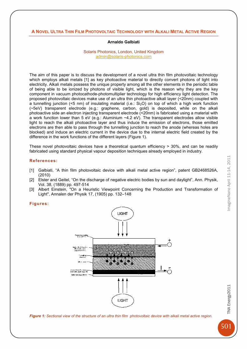
The aim of this paper is to discuss the development of a novel ultra thin film photovoltaic technology which employs alkali metals [1] as key photoactive material to directly convert photons of light into electricity. Alkali metals possess the unique property among all the other elements in the periodic table of being able to be ionized by photons of visible light, which is the reason why they are the key component in vacuum photocathode-photomultiplier technology for high efficiency light detection. The proposed photovoltaic devices make use of an ultra thin photoactive alkali layer (<20nm) coupled with a tunnelling junction (<5 nm) of insulating material (i.e.: Si2O) on top of which a high work function (~5eV) transparent electrode (e.g.: graphene, carbon, gold) is deposited, while on the alkali photoactive side an electron injecting transparent electrode (<20nm) is fabricated using a material with a work function lower than 5 eV (e.g.: Aluminium ~4.2 eV). The transparent electrodes allow visible light to reach the alkali photoactive layer and thus induce the emission of electrons, those emitted electrons are then able to pass through the tunnelling junction to reach the anode (whereas holes are blocked) and induce an electric current in the device due to the internal electric field created by the difference in the work functions of the different layers (Figure 1). These novel photovoltaic devices have a theoretical quantum efficiency > 30%, and can be readily fabricated using standard physical vapour deposition techniques already employed in industry. References: [1] Galbiati, “A thin film photovoltaic device with alkali metal active region”, patent GB2468526A,
(2010) [2] Elster and Geitel, “On the discharge of negative electric bodies by sun and daylight”, Ann. Physik,
Vol. 38, (1889) pp. 497-514 [3] Albert Einstein, "On a Heuristic Viewpoint Concerning the Production and Transformation of
Light", Annalen der Physik 17, (1905) pp. 132–148 Figures:
Figure 1: Sectional view of the structure of an ultra thin film photovoltaic device with alkali metal active region.

TNA
TNA
TNA
TNA Energy
Energy
Energy
Energy 2011
2011
2011
2011
ImagineNano April 11-14, 2011
502

TNA
TNA
TNA
TNA Energy
Energy
Energy
Energy 2011
2011
2011
2011
ImagineNano April 11-14, 2011
503
SYNTHESIS OF HIGH-SURFACE-AREA PLATINUM NANOTUBES USING A VIRAL TEMPLATE
Marcin Ł. Górzny1,2
, Alex S. Walton2, Stephen D. Evans2, Alexander Bittner1
1CIC nanoGUNE Consolider, Tolosa Hiribidea, 76, E-20018 Donostia – San Sebastian, Spain, 2School of Physics and Astronomy, University of Leeds, Woodhouse Lane, LS2 9JT, Leeds, UK
The demand for green, efficient, low-cost, portable energy supplies has never been greater. One promising approach is the use of fuel cells such as the direct methanol fuel cell (DMFC). These promise significant increase (×10) energy density storage over conventional lithium-ion batteries, with potential to reach levels of 4.8 kWhL−1 (or 6.1 Whg−1). A key component in such DMFCs is the anode, at which methanol is oxidized, to produce carbon dioxide, hydrogen ions and electrons. Platinum (and its alloys) has proven to be a material with strong potential for use as an anode, due to its ability to adsorb hydrogen. A novel method for the synthesis of high surface area, Platinum - Tobacco mosaic virus (Pt-TMV) nanotubes is presented. Platinum salt is reduced to metallic form on the external surface of a rodshaped TMV by methanol, which serves as a solvent and reductant simultaneously. The method provides enhanced control of surface roughness and Pt thickness than under strongly reducing conditions (eg DMAB or NaBH4). It was found that for the same Pt loading, Pt-TMV nanotubes had electrochemically active surface area (ECSA) 3.7 times larger than Pt nanoparticles. The Pt-TMV system, used as a catalyst for methanol oxidation, shows 65% higher catalytic mass activity than catalyst based on Pt nanoparticles [1]. Whilst we present results for coating of TMV, the route is more general and should work on any charged protein/surfactant system. References: [1] Marcin Ł. Górzny, Alex S. Walton, and Stephen D. Evans, Adv. Funct. Mater., 2010, 20, 1295-
1300 Figures:
Figure 1: TEM image of Pt-TMV nanotube (a). Panel b, shows two cyclic voltammogram curves corre sponding to Pt-TMV (red trace) and PtNPs (green trace) in 0.5 M H2SO4. Peaks A, B and C correspond to hydrogen adsorption on Pt(110), Pt(100) and Pt(111) crystal planes respectively. These characteristics were used to evaluate the surface area. Panel b shows a cyclic voltammogram curves for the oxidation of methanol. Two CV curves corresponding to Pt-TMV (red trace) and PtNPs (green trace) in mixture of 0.5 M H2SO4 and 2 M CH3OH, nitrogen purged, sweep rate 100 mVs
−1.

TNA
TNA
TNA
TNA Energy
Energy
Energy
Energy 2011
2011
2011
2011
ImagineNano April 11-14, 2011
504
TNA
TNA
TNA
TNA Energy
Energy
Energy
Energy 2011
2011
2011
2011
ImagineNano April 11-14, 2011
505
THE ADVENT OF MESOSOCOPIC SOLAR CELLS
Michael Graetzel
Laboratory of Photonics and Interfaces, Ecole Polytechnique Fédérale de Lausanne, Station 6,LPI EPFL, CH-1015, Lausanne, Switzerland
The field of photovoltaic cells has been dominated so far by solid state p-n junction devices made e.g. of crystalline or amorphous silicon or other chalcogenide semiconductors, profiting from the experience and material availability of the semiconductor industry. However, there is an increasing awareness of the possible advantages of devices referred to as “bulk“ junctions due to their interconnected three-dimensional structure. Their embodiment departs completely from the conventional flat p-n junction solid-state cells, replacing them by interpenetrating networks. This lecture focuses on dye sensitized and quantum dot sensitized mesoscopic solar cells (DSCs), which are leading this new generation of photovoltaic devices [1-4]. Imitating the light reaction of natural photo-synthesis, this cell is the only photovoltaic system that uses molecules to generate charges from sunlight accomplishing the separation of the optical absorption from the charge separation and carrier transport processes. It does so by associating a molecular dye with a mesoscopic film of a large band gap semiconductor oxide. The DSC has made phenomenal progress, present conversion efficiencies being over 12 percent for single junction and 17 percent for tandem cells. The validated module efficiency has reached 10 percent, rendering the DSC a credible alternative to conventional thin film p-n junction devices. Commercial large-scale production of flexible DSC modules has started in 2009. These solar cells have become viable contenders for large-scale future solar energy conversion systems on the bases of cost, efficiency, stability and availability as well as environmental compatibility. References: [1] B. O’Regan and M. Grätzel , Nature, London 353 (1991). [2] U.Bach, D.Lupo, P.Comte, J.E.Moser, F.Weissörtel, J.Salbeck, H.Spreitzert and M.Grätzel,
Nature, 395, 550 (1998). [3] M Grätzel , Nature 414, 338344 (2001). [4] M.Grätzel, Acc. Chem. Res. 42, 1781-1798 (2009).

TNA
TNA
TNA
TNA Energy
Energy
Energy
Energy 2011
2011
2011
2011
ImagineNano April 11-14, 2011
506
TNA
TNA
TNA
TNA Energy
Energy
Energy
Energy 2011
2011
2011
2011
ImagineNano April 11-14, 2011
507
OPTICALLY TRANSPARENT CATHODE FOR DYE SENSITIZED SOLAR CELLS BASED ON GRAPHENE
NANOPLATELETS
Ladislav Kavan1,2*, Jun Ho Yum2 and Michael Grätzel
1J. Heyrovský Institute of Physical Chemistry, v.v.i., Academy of Sciences of the Czech Republic, Dolejškova 3, CZ-18223 Prague 8, Czech Republic
2Laboratory of Photonics and Interfaces, Institute of Chemical Sciences and Engineering, Swiss Federal Institute of Technology, CH-1015 Lausanne, Switzerland
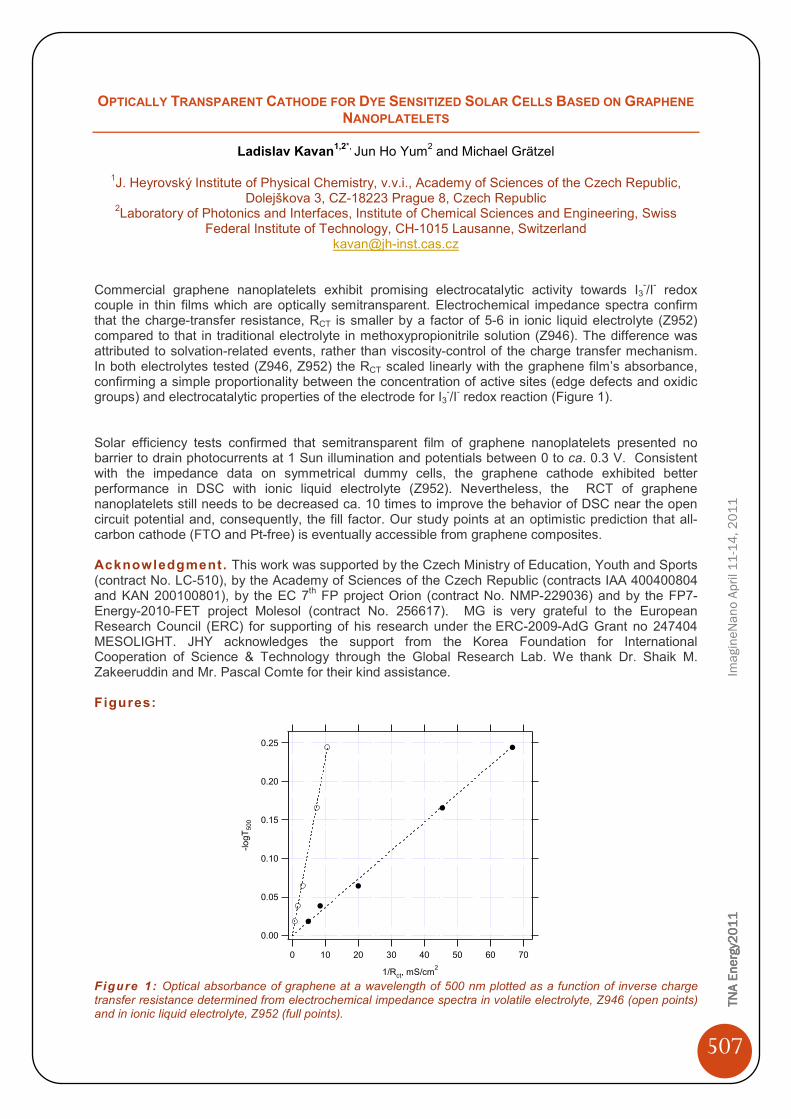
Commercial graphene nanoplatelets exhibit promising electrocatalytic activity towards I3
-/I- redox couple in thin films which are optically semitransparent. Electrochemical impedance spectra confirm that the charge-transfer resistance, RCT is smaller by a factor of 5-6 in ionic liquid electrolyte (Z952) compared to that in traditional electrolyte in methoxypropionitrile solution (Z946). The difference was attributed to solvation-related events, rather than viscosity-control of the charge transfer mechanism. In both electrolytes tested (Z946, Z952) the RCT scaled linearly with the graphene film’s absorbance, confirming a simple proportionality between the concentration of active sites (edge defects and oxidic groups) and electrocatalytic properties of the electrode for I3
-/I- redox reaction (Figure 1). Solar efficiency tests confirmed that semitransparent film of graphene nanoplatelets presented no barrier to drain photocurrents at 1 Sun illumination and potentials between 0 to ca. 0.3 V. Consistent with the impedance data on symmetrical dummy cells, the graphene cathode exhibited better performance in DSC with ionic liquid electrolyte (Z952). Nevertheless, the RCT of graphene nanoplatelets still needs to be decreased ca. 10 times to improve the behavior of DSC near the open circuit potential and, consequently, the fill factor. Our study points at an optimistic prediction that all-carbon cathode (FTO and Pt-free) is eventually accessible from graphene composites. Acknowledgment. This work was supported by the Czech Ministry of Education, Youth and Sports (contract No. LC-510), by the Academy of Sciences of the Czech Republic (contracts IAA 400400804 and KAN 200100801), by the EC 7th FP project Orion (contract No. NMP-229036) and by the FP7-Energy-2010-FET project Molesol (contract No. 256617). MG is very grateful to the European Research Council (ERC) for supporting of his research under the ERC-2009-AdG Grant no 247404 MESOLIGHT. JHY acknowledges the support from the Korea Foundation for International Cooperation of Science & Technology through the Global Research Lab. We thank Dr. Shaik M. Zakeeruddin and Mr. Pascal Comte for their kind assistance. Figures:
0.25
0.20
0.15
0.10
0.05
0.00
-logT
50
0
706050403020100
1/Rct, mS/cm2
Figure 1: Optical absorbance of graphene at a wavelength of 500 nm plotted as a function of inverse charge transfer resistance determined from electrochemical impedance spectra in volatile electrolyte, Z946 (open points) and in ionic liquid electrolyte, Z952 (full points).

TNA
TNA
TNA
TNA Energy
Energy
Energy
Energy 2011
2011
2011
2011
ImagineNano April 11-14, 2011
508

TNA
TNA
TNA
TNA Energy
Energy
Energy
Energy 2011
2011
2011
2011
ImagineNano April 11-14, 2011
509
INDIRECT NANOPLASMONIC SENSING IN CATALYSIS: SINTERING, REACTANT SURFACE
COVERAGE CHANGES AND OPTICAL NANOCALORIMETRY
Elin M. Larsson1,2,3, Christoph Langhammer1,2, Julien Millet1, Stefan Gustafsson1, Eva Olsson1, Igor
Zoric1, Magnus Skoglundh3, Bengt Kasemo1
1Applied Physics, Chalmers University of Technology, Fysikgränd 3, Gothenburg, Sweden
2 Insplorion AB, Ekmansgatan 3, Gothenburg, Sweden 3 Competence Center for Catalysis, Chalmers Univ of Technology, Kemigården, Gothenburg, Sweden
We report four different application areas, within catalysis, of a new “nanoplasmonic” (localized surface plasmon resonance, LSPR) method, Indirect Nanoplasmonic Sensing (INPS), which uses a remarkably simple optical transmission (or reflection) measurement. The method can with high sensitivity follow catalytic reactions in real time in-situ and can be applied to both model catalysts and real supported catalysts at realistic catalyst working conditions (i.e. high pressures and temperatures). A catalyst is a substance that increases the rate of a reaction without itself being destroyed or consumed. Many industrial processes as well as the environmental and energy sectors depend on catalysis. Some of the most important uses for catalysts are to decrease the need for energy and raw materials and to clean industrial and automotive exhausts. To understand and improve heterogeneous catalyst systems it is important to be able to monitor the catalyst’s state and to follow the reaction in real time. However, there is still a need for new experimental probes that allow such investigations to be made on the often complex catalyst structures and under realistic catalyst working conditions. Here we present a technique that has the potential to partly fill this need. We show that INPS can be used to monitor changes in adsorbed species on nanoparticle catalysts or chemical changes in a thin film [1], for optical nanocalorimetry [2] and to monitor sintering [3]. Sintering is the deactivation of a catalyst by the coalescence of catalytically active nanoparticles to form larger less active particles. Catalyst sintering causes large economic and environmental costs associated with catalyst regeneration/renewal. The principle is “nanoplasmonic” sensing, which has been intensely investigated for biosensing. A LSPR is a coherent resonance oscillation of the conduction electrons, a plasmon resonance, in a metal nanoparticle, which can be excited by near-visible light with an appropriate color/wavelength. The wavelength at which the resonance occurs depends e.g. on the dielectric properties of the particle’s nanoenvironment and can, therefore, be use for sensing where dielectric changes are to be detected [4]. INPS applies a patent searched [5] sensor chip design (see figure 1A) which allows events such as sintering, surface coverage changes[1], and hydrogen storage [2, 6] in/on nanoparticles/clusters/thin films to be monitored using the plasmon resonance of other nanoparticles in their close vicinity. The INPS technology is being commercialized by Insplorion AB that markets and sells research instruments. Figure 1B shows real-time data from the storage (8 to 38 minutes) and release (from 38 minutes, induced by adding hydrogen) of nitrogen oxides (NOx) in/from a barium compound [1]. The data shows that the reaction can be monitored with high sensitivity and time resolution and that the obtained signal is concentration dependent. The reaction studied here is relevant in NOx storage and release catalysts extensively researched for lean burn automotive engines and shows that INPS can be used to study such reactions or as a nitrogen oxide sensor. We also show that a change in surface adsorbate from oxygen to hydrogen/carbon monoxide can be monitored with sub-monolayer sensitivity using INPS[1]. For optical nanocalorimetry it is utilized that the plasmon resonance is sensitive to temperature changes. Figure 1C shows light off traces obtained for Pd nanoparticles (average diameter 18.6 nm) deposited on an INPS sensor chip. The Pd particles were exposed to mixtures of hydrogen and oxygen (α= relative hydrogen concentration, total reactant concentration was kept constant) and the external temperature was increased linearly. Figure 1C shows the data after correction for the external temperature change. The data shows a rapid increase in the catalyst temperature at catalytic light off. The peak shift obtained at high temperatures depends on the α-value as expected (different α values

TNA
TNA
TNA
TNA Energy
Energy
Energy
Energy 2011
2011
2011
2011
ImagineNano April 11-14, 2011
510
give different maximum reaction rates). We also demonstrate that INPS can be used to study particle size dependent reactivity [2]. In the last application, it is demonstrated that INPS can be used for real-time and intermittent monitoring of catalytic cluster sintering. Sintering of Pt clusters, similar to those in the car exhaust catalyst, was monitored in different gas environments at atmospheric pressure on SiO2 surfaces. Substantially increased sintering rate were observed in 4% O2 (in Ar) as compared to in pure Ar. As expected, the sintering rate was also found to increase with increasing temperature (see figure 1D). The optical signal obtained during sintering was calibrated using post-mortem TEM imaging of TEM-window samples, identical to the optical/glass samples, which were run in parallel with the optical measurements. The obtained data show that INPS is a promising novel technique for real-time measurements of the catalyst state and nanocalorimetry using a low cost, optical transmission/reflection measurement. References: [1] E.M. Larsson, C. Langhammer, I. Zoric, B. Kasemo , Science, 326 (2009) 1091 [2] C. Langhammer, E.M. Larsson, B.Kasemo, I. Zorić, Nano Letters 10 (2010) 3529 [3] E. M. Larsson, C. Langhammer, J. Millet1, S. Gustafsson, E. Olsson, I. Zoric, M. Skoglundh, B.
Kasemo, In preparation [4] E.M. Larsson, J. Alegret, M. Käll, D.S. Sutherland, Nano Letters 7 (2007) 1256 [5] C. Langhammer, E.M. Larsson, I. Zorić, B. Kasemo, Swedish patent application number
0950368-1. Filed May 2009 [6] C. Langhammer, V. Zdanov, B. Kasemo, I. Zorić, Review Letters, 104 (2010) 135502 Figures:
TNA
TNA
TNA
TNA Energy
Energy
Energy
Energy 2011
2011
2011
2011
ImagineNano April 11-14, 2011
511
SILICON NANOWIRES AND NANOPILLARS ARRAYS FOR LITHIUM-ION BATTERY AND MICRO-BATTERY: OVERVIEW, CHALLENGES AND PERSPECTIVES
C. Lethien, M. Zegaoui, N. Rolland and P.A Rolland
IEMN CNRS UMR 8520 and IRCICA CNRS USR 3380 Avenue Poincaré, BP 60069, 59652 Villeneuve d'Ascq cedex, France
Université Lille Nord de France
Nowadays, energy autonomy appears to be the main challenge for hybrid/electrical vehicles as well as nomadic electronic devices. Coin and rechargeable batteries remain the only available sources to supply such devices. The energy autonomy is a societal and critical issue and the nanotechnology could help the research community to improve the devices performances in particular in the field of lithium ion battery/micro-battery. A classical lithium ion storage device is composed of a positive electrode (mainly LiCoO2), a lithium ion electrolyte (liquid or solid) and a negative electrode (graphite). The capacity of the graphite electrode is unfortunately limited to 372 mAh/g. The silicon material appears to be a promising candidate for the negative electrode as it has the potential to be a host material for the lithium ion Li+ with the highest reported specific capacity close to 4200 mAh/g. Unfortunately, the lithiation process (insertion of the lithium ion into the silicon crystal) occurring during the battery charging leads to a silicon’s volume variation of 300 %. The high volume expansion of the silicon crystal remains the main cause of both the capacity fading and the pulverization of the fabricated battery. The lifetime of the lithium ion battery based on silicon material is then considerably reduced. Several research groups have developed novel negative electrode topologies using nanostructured silicon material in order to overcome the problem of the volume variation [1-6]. A negative electrode based on silicon material with an empty rate close to 50 % and allowing a volumetric expansion of the silicon crystal owing to the lithiation process is generally proposed. To obtain such empty electrodes, the nanotechnology seems to be a useful tool. Two different approaches could be investigated to produce silicon nanowires or nanopillars array. The bottom up way consists in the growth of silicon nanowires by Chemical Vapor Deposition (CVD) on stainless steel substrate according to the well known Vapor-Liquid-Solid (VLS) or Vapor-Solid (VS) processes. The 2nd path way (top down development) is based on the micromachining of the silicon material either by wet or dry etching [7-8]. This paper reports an overview of the silicon nanowires or nanopillars acting as a negative electrode of a lithium-ion battery or micro-battery. The bottom up (CVD synthesis) and top down (wet or dry etching) approaches will be compared. The potentialities of the silicon nanowires/nanopillars and their integration in a lithium-ion battery or micro-battery will be discussed. An original SiNPL micromachining processes using Deep Reactive Ion Etching and photolithography technologies will be presented. In the depicted process, the SiNPL array is obtained without electron beam nanolithography. References: [1] B. Laïk, L. Eude, J.-P. Pereira-Ramos, C. S. Cojocaru, D. Pribat and E. Rouvière 2008
Electrochimica Acta 53 5528-5532 [2] CK. Chan, H. Peng, G. Liu, K. McIlwrath, X. F. Zhang, R. A. Huggins, Y. Cui 2008 Nature
Nanotech. 3 31-35 [3] CK. Chan, R. Ruffo, SS. Hong, RA. Huggins and Yi Cui 2009 Journal of Power Sources 189 34–
39 [4] Liangbing Hu, Hui Wu, Seung Sae Hong, Lifeng Cui, James R. McDonough, SY Bohy and Yi Cui
2010 Chem Commun 47 367-369 [5] Barbara Laïk, Diane Ung, Amaël Caillard, Costel Sorin Cojocaru, Didier Pribat, Jean-Pierre
Pereira-Ramos 2010 J Solid State Electrochem 14 1835–1839 [6] Jang Wook Choi, James McDonough, Sangmoo Jeong, Jee Soo Yoo, Candace K. Chan and Yi
Cui 2010 Nano Letters 10 1409–1413 [7] K. Peng et al 2008 Applied Physics Letters 93, 033105-1 033105-3 [8] C. Lethien et al 2011 submitted to Microelectronic Engineering
TNA
TNA
TNA
TNA Energy
Energy
Energy
Energy 2011
2011
2011
2011
ImagineNano April 11-14, 2011
512
Figures: (a)
(b)
(c)
(d)
(e)
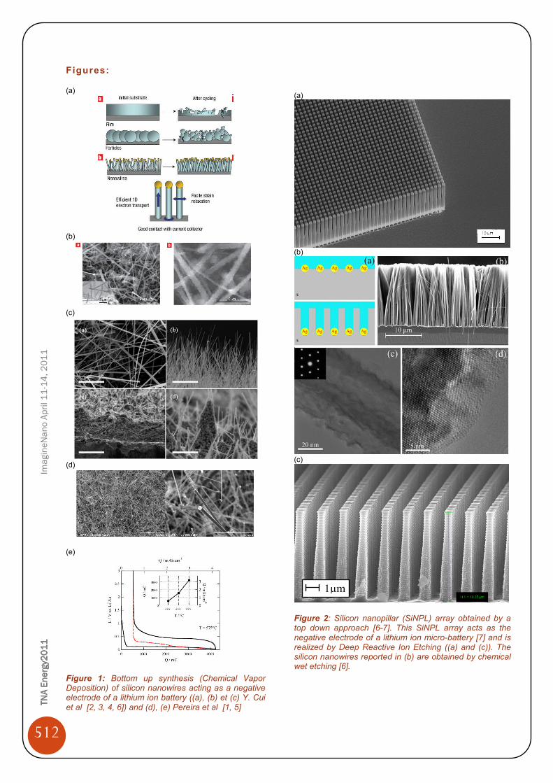
Figure 1: Bottom up synthesis (Chemical Vapor Deposition) of silicon nanowires acting as a negative electrode of a lithium ion battery ((a), (b) et (c) Y. Cui et al [2, 3, 4, 6]) and (d), (e) Pereira et al [1, 5]
(a)
(b)
(c)
1µm
Figure 2: Silicon nanopillar (SiNPL) array obtained by a top down approach [6-7]. This SiNPL array acts as the negative electrode of a lithium ion micro-battery [7] and is realized by Deep Reactive Ion Etching ((a) and (c)). The silicon nanowires reported in (b) are obtained by chemical wet etching [6].

TNA
TNA
TNA
TNA Energy
Energy
Energy
Energy 2011
2011
2011
2011
ImagineNano April 11-14, 2011
513
NANOTECHNOLOGY FOR MORE EFFICIENT PHOTOVOLTAICS: THE QUANTUM DOT INTERMEDIATE BAND SOLAR CELL
Antonio Luque
Instituto de Energía Solar, Universidad Politécnica de Madrid, 28040 Madrid, Spain [email protected]
The intermediate band solar cell [1] has been proposed as a concept able to substantially enhance the efficiency limit of an ordinary single junction solar cell. If a band permitted for electrons is inserted within the forbidden band of a semiconductor then a novel path for photo generation is open: electron hole pairs may be formed by the successive absorption of two sub bandgap photons using the intermediate band (IB) as a stepping stone. While the increase of the photovoltaic (PV) current is not a big achievement —it suffices to reduce the bandgap— the achievement of this extra current at high voltage is the key of the IB concept. In ordinary cells the voltage is limited by the bandgap so that reducing it would also reduce the bandgap. In the intermediate band solar cell the high voltage is produced when the IB is permitted to have a Quasi Fermi Level (QFL) different from those of the Conduction Band (CB) and the Valence Band (VB). For it the cell must be properly isolated from the external contacts, which is achieved by putting the IB material between two n- and p-type ordinary semiconductors [2]. Efficiency thermodynamic limit of 63% is obtained for the IB solar cell1 vs. the 40% obtained [3] for ordinary single junction solar cells. Detailed information about the IB solar cells can be found elsewhere [4]. IB solar cells may be implemented by nanotechnology [5]. In particular the IB can be formed by the bound states of quantum dots of a lower gap semiconductor located inside a wider bandgap host semiconductor. The first practical realization was made with InAs QDs in a GaAs matrix [6]. Other groups have prepared similar devices [7-11]. Highest efficiency so far has been 18% [10]. In reality present QD IB solar cells present a negligible increase of the photocurrent and a substantial reduction of the voltage so that they always present less efficiency than test structures of the same host semiconductor without QDs. As matter of fact one of the reasons of this reduced efficiency is that the InAs/GaAs system is very inappropriate. The increased thermodynamic efficiency limit is achieved for a bandgap of about 2 eV and a position of the IB band at 0.7 e.V from the CB whereas in the InAs/GaAs system has a total bandgap of 1.42 eV at room temperature and the position of the IB is at about 0.25-0.30 eV form the GaAs CB. Calculations [12] show that for these bandgaps the one-sun efficiency (the one referred to in all the cited publications) cannot exceed that of the cell without IB although the case might be different under concentrated sunlight. However, this materials system has permitted to experimentally prove the operational principles of this concept, namely the two photon mechanism [13] and the three QFL splitting [14] and its direct consequence, the achievement of voltage very close to the GaAs badgap [15]. Unfortunately this has only been possible to detect [13] or achieve [15] at very low temperature when the thermal escape has been suppressed. The reduction of voltage of present QD IB solar cells is partly due to the reduction of minority carrier lifetime introduced through the dislocations created by the stresses. This has been amended by stress reduction of spacer increase and is not a major problem today. In part it is also due to the reduction of the bandgap due to the invasion of the bandgap by the heavy hole states [12,16] that form a quasi continuous, and by the formation of a wetting later that acts as a quantum well [12]. According to this, it is unfair use single gap cell without QDs with the cell with QDs in the same host material. Changing the bandgap of the host material this problem is solved. Yet the increase of current is very small and this is due by an inherent low absorption of the QDs for interband transitions. We think that the CB wavefunctions have an envelope with S symmetry [16] while this symmetry is absent in the VB wavefunctions. The consequence is that the relevant envelope wavefunctions overlap poorly. We don’t know yet the solution to this issue, besides, of course, a photon management strategy to enhance the absorption. Finally another issue is the thermal escape. It prevents form an easy splitting of the CB and IB QFLs. Best solutions are the reduction of the QD size to prevent QD excited states that may provide a ladder

TNA
TNA
TNA
TNA Energy
Energy
Energy
Energy 2011
2011
2011
2011
ImagineNano April 11-14, 2011
514
for the escape of electrons [17] and, of course, to change the material system to better exploit the potentialities of the concept [18]. References: [1] A. Luque and A. Martí, Physical Review Letters 78, 5014–5017 (1997). [2] A. Luque and A. Martí, Progress in Photovoltaics: Res. Appl. 9, 73–86 (2001). [3] W. Shockley and H. J. Queisser, Journal of Applied Physics 32, 510-519 (1961). [4] A. Luque and A. Marti, Advanced Materials 22, 160-174 (2009). [5] A. Martí, L. Cuadra, and A. Luque, in Proc. 28th IEEE Photovoltaics Specialists Conference
(IEEE, New York, 2000), p. 940-943. [6] A. Luque, A. Martí, C. Stanley, N. López, L. Cuadra, D. Zhou, and A. Mc-Kee, Journal of Applied
Physics 96, 903–909 (2004). [7] S. M. Hubbard, C. D. Cress, C. G. Bailey, R. P. Raffaelle, S. G. Bailey, and D. M. Wilt, Applied
Physics Letters 92, 123512 (2008). [8] V. Popescu, G. Bester, M. C. Hanna, A. G. Norman, and A. Zunger, Physical Review B 78,
205321 (2008). [9] R. Oshima, A. Takata, and Y. Okada, Applied Physics Letters 93, 083111 (2008). [10] S. A. Blokhin, A. V. Sakharov, A. M. Nadtochy, A. S. Pauysov, M. V. Maximov, N. N. Ledentsov,
A. R. Kovsh, S. S. Mikhrin, V. M. Lantratov, S. A. Mintairov, N. A. Kaluzhniy, and M. Z. Shvarts, Semiconductors 43, 514–518 (2009).
[11] D. Alonso-Alvarez, A. G. Taboada, J. M. Ripalda, B. Alen, Y. Gonzalez, L. Gonzalez, J. M. Garcia, F. Briones, A. Marti, A. Luque, A. M. Sanchez, and S. I. Molina, Applied Physics Letters 93, 123114 (2008).
[12] A. Marti, E. Antolin, E. Canovas, N. Lopez, P. G. Linares, A. Luque, C. R. Stanley, and C. D. Farmer, Thin Solid Films 516, 6716-6722 (2008).
[13] A. Marti, E. Antolin, C. R. Stanley, C. D. Farmer, N. Lopez, P. Diaz, E. Canovas, P. G. Linares, and A. Luque, Physical Review Letters 97, 247701-4 (2006).
[14] A. Luque, A. Marti, N. Lopez, E. Antolin, E. Canovas, C. Stanley, C. Farmer, L. J. Caballero, L. Cuadra, and J. L. Balenzategui, Applied Physics Letters 87, 083505-3 (2005).
[15] E. Antolín, A. Martí, P. G. Linares, I. Ramiro, E. Hernández, C. D. Farmer, C. R. Stanley, and A. Luque, in Proc.25 Photovoltaic Specialists Conference (IEEE, Honolulu, 2010).
[16] A. Luque, A. Marti, E. Antolín, P. G. Linares, I. Tobías, I. Ramiro, and E. Hernandez, Solar Energy Materials & Solar Cells, to be published (2011).
[17] A. Luque, A. Marti, E. Antolín, P. G. Linares, I. Tobias, and I. Ramiro, submitted (2011). [18] P. G. Linares, A. Marti, E. Antolin, and A. Luque, Journal of Applied Physics 109, 014313 (2011).
TNA
TNA
TNA
TNA Energy
Energy
Energy
Energy 2011
2011
2011
2011
ImagineNano April 11-14, 2011
515
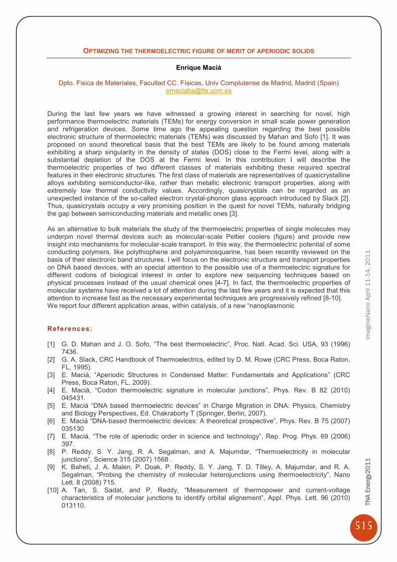
OPTIMIZING THE THERMOELECTRIC FIGURE OF MERIT OF APERIODIC SOLIDS
Enrique Maciá
Dpto. Fisica de Materiales, Facultad CC. Físicas, Univ Complutense de Madrid, Madrid (Spain) [email protected]
During the last few years we have witnessed a growing interest in searching for novel, high performance thermoelectric materials (TEMs) for energy conversion in small scale power generation and refrigeration devices. Some time ago the appealing question regarding the best possible electronic structure of thermoelectric materials (TEMs) was discussed by Mahan and Sofo [1]. It was proposed on sound theoretical basis that the best TEMs are likely to be found among materials exhibiting a sharp singularity in the density of states (DOS) close to the Fermi level, along with a substantial depletion of the DOS at the Fermi level. In this contribution I will describe the thermoelectric properties of two different classes of materials exhibiting these required spectral features in their electronic structures. The first class of materials are representatives of quasicrystalline alloys exhibiting semiconductor-like, rather than metallic electronic transport properties, along with extremely low thermal conductivity values. Accordingly, quasicrystals can be regarded as an unexpected instance of the so-called electron crystal-phonon glass approach introduced by Slack [2]. Thus, quasicrystals occupy a very promising position in the quest for novel TEMs, naturally bridging the gap between semiconducting materials and metallic ones [3]. As an alternative to bulk materials the study of the thermoelectric properties of single molecules may underpin novel thermal devices such as molecular-scale Peltier coolers (figure) and provide new insight into mechanisms for molecular-scale transport. In this way, the thermoelectric potential of some conducting polymers, like polythiophene and polyaminosquarine, has been recently reviewed on the basis of their electronic band structures. I will focus on the electronic structure and transport properties on DNA based devices, with an special attention to the possible use of a thermoelectric signature for different codons of biological interest in order to explore new sequencing techniques based on physical processes instead of the usual chemical ones [4-7]. In fact, the thermoelectric properties of molecular systems have received a lot of attention during the last few years and it is expected that this attention to increase fast as the necessary experimental techniques are progressively refined [8-10]. We report four different application areas, within catalysis, of a new “nanoplasmonic References: [1] G. D. Mahan and J. O. Sofo, “The best thermoelectric”, Proc. Natl. Acad. Sci. USA, 93 (1996)
7436. [2] G. A. Slack, CRC Handbook of Thermoelectrics, edited by D. M. Rowe (CRC Press, Boca Raton,
FL, 1995). [3] E. Maciá, “Aperiodic Structures in Condensed Matter: Fundamentals and Applications” (CRC
Press, Boca Raton, FL, 2009). [4] E. Maciá, “Codon thermoelectric signature in molecular junctions”, Phys. Rev. B 82 (2010)
045431. [5] E. Maciá “DNA based thermoelectric devices” in Charge Migration in DNA: Physics, Chemistry
and Biology Perspectives, Ed. Chakraborty T (Springer, Berlin, 2007). [6] E. Maciá “DNA-based thermoelectric devices: A theoretical prospective”, Phys. Rev. B 75 (2007)
035130 [7] E. Maciá, “The role of aperiodic order in science and technology”, Rep. Prog. Phys. 69 (2006)
397. [8] P. Reddy, S. Y. Jang, R. A. Segalman, and A. Majumdar, “Thermoelectricity in molecular
junctions”, Science 315 (2007) 1568 . [9] K. Baheti, J. A. Malen, P. Doak, P. Reddy, S. Y. Jang, T. D. Tilley, A. Majumdar, and R. A.
Segalman, “Probing the chemistry of molecular heterojunctions using thermoelectricity”, Nano Lett. 8 (2008) 715.
[10] A. Tan, S. Sadat, and P. Reddy, “Measurement of thermopower and current-voltage characteristics of molecular junctions to identify orbital alignement”, Appl. Phys. Lett. 96 (2010) 013110.
TNA
TNA
TNA
TNA Energy
Energy
Energy
Energy 2011
2011
2011
2011
ImagineNano April 11-14, 2011
516
Figures:
Figure 1 : Sketch illustrating the basic features of a nanoscale DNA based Peltier cell. A polyA-polyT (polyG-polyC) oligonucleotide, playing the role of n-type, left (p-type, right) semiconductor legs, are connected to organic wires (light boxes) deposited onto ceramic heat sinks (dark boxes).
TNA
TNA
TNA
TNA Energy
Energy
Energy
Energy 2011
2011
2011
2011
ImagineNano April 11-14, 2011
517
NANOENGINEERING THERMOELECTRICS FOR ENERGY HARVESTING.
Marisol Martin-Gonzalez
Thermoelectrics Group, Instituto de Microelectrónica de Madrid, IMM-CNM-CSIC. Tres Cantos Madrid (Spain) [email protected]
The growing social alarm over increasing energy cost and global warming related to fossil fuel sources has motivated the search for cleaner, more sustainable energy sources. Among the different feasible technologies, thermoelectric (TE) devices have received attention as these solid-state devices can generate electricity by harvesting waste thermal energy, thereby improving the efficiency of a system. The many advantages of TE devices include solid-state operation, no noise, zero-emissions, vast scalability, no maintenance and a long operating lifetime. The efficiency of TE materials is directly related to a dimensionless figure of merit (ZT). In order to compete with conventional refrigerators, a ZT=3 must be obtained. Although, a device with ZT>2 will be also important in other applications. Due to their limited energy conversion efficiencies (i.e. ZT is ≈1), thermoelectric devices currently are only present in niche applications. However, there is a renewed interest in the field of thermoelectrics due to quantum size effects, which provide additional ways to enhance energy conversion efficiencies in nanostructured materials. For example, a ZT up to 2.5 was achieved by synthesizing two-dimensional Sb2Te3/Bi2Te3 superlattice thin films through a chemical vapor deposition (CVD) process, exceeding previous limits of ≈1 for bulk counterparts; theoretical calculations predict that even higher ZTs can be achieved in one-dimensional nanowires. The successful application of these nanostructures in practical thermoelectric devices must implement a cost-effective and high through-put fabrication process. Among the different techniques electrodeposition has been one of the more successful. For that reason an overview of the state of the art in the electrodeposition, of films and nanowires, of the different thermoelectric: Chalkogenide, Silizide SiGe, TAGS, Skutterudites, Clathrates, etc will be presented here. Acknowledgments: ERC Starting Grant 2008: 240497

TNA
TNA
TNA
TNA Energy
Energy
Energy
Energy 2011
2011
2011
2011
ImagineNano April 11-14, 2011
518

TNA
TNA
TNA
TNA Energy
Energy
Energy
Energy 2011
2011
2011
2011
ImagineNano April 11-14, 2011
519
NEW ROUTES FOR THE FABRICATION OF ORGANIC PHOTOVOLTAIC CELLS
Jordi Martorell
ICFO-Institut de Ciencies Fotoniques, 08860 Castelldefels (Barcelona), Spain and Departament de Fisica i Enginyeria Nuclear, Universitat Politecnica de Catalunya,
08222 Terrassa, Spain Organic solar cells have been the subject of research for the realization of portable, flexible and transparent modules as renewable energy sources. Here we propose alternative routes to fabricate such type of devices using simple and cost effective fabrication methods based on, the replacement of electron blocking layers by sputtered NiO, the substitution of the ITO electrode by a sputtered thin metal film, and on the fabrication of the organic photovoltaic cells using a dip coating procedure instead of a spin coating one.
Table 1: Performance of Cu-Ni electrode based cells compared to ITO based cells
We fabricated and tested the performance of P3HT:PCBM bulk hetero-junction solar cells when the PEDOT:PSS, the most commonly used hole transporting layer, is replaced by a thin layer of sputtered NiO, and when the transparent indium tin oxide (ITO) electrode is replaced by a sputtered ultra-thin Cu-Ni bilayer. We show, here, that when NiO is used as the hole transporting layer, the characteristic photovoltaic parameters of such cell are similar or better to those of the device fabricated with PEDOT:PSS. We also studied the lifetime of NiO based cells in comparison to the PEDOT:PSS based ones. We observed that an ambient air processing of the organic materials was not detrimental to the ulterior performance of the NiO based cell, which degraded in ambient air conditions with a time constant larger than 300 hours. On the contrary, the PEDOT:PSS cell degraded very rapidly and the loss in efficiency was shown to be 29 times faster when compared to the NiO cell.
Figure 1: I-V curves for P3HT/PCBM cells fabricated using ITO (black), Cu(7 nm)-Ni(1 nm) (blue), and Cu(9 nm)-Ni(1 nm) (red).
In such NiO based cells we also used a Cu-Ni semi-transparent electrode to replace the ITO. Despite the fact that the metal electrode exhibits a transparency that is 65% of the ITO electrode, the short circuit current for the metallic anode based cell is 77% of the ITO based one (see Table 1), which exhibited a power conversion efficiency of 3.3% (see Figure 1). Such discrepancy between the transparency and short circuit current percentage indicates that photon absorption may be enhanced by the optical microcavity formed between the Cu-Ni and Al electrodes. We also fabricated organic solar cells with a bilayer architecture, in which poly(p-phenylene vinylene) (PPV) was used as the electron donor while Rhodamine 6G as the electron acceptor. We showed that photo-conversion efficiency for such dip coated fabricated cells is 1.4 times higher than that obtained from cells fabricated using the traditional spin coating procedure. Comparing the performance of several cells produced by dip coating on the same substrate we observed a high degree of uniformity, as opposed to the performance of the spin coated cells which exhibited a large dispersion. In addition,

TNA
TNA
TNA
TNA Energy
Energy
Energy
Energy 2011
2011
2011
2011
ImagineNano April 11-14, 2011
520
when the dip coating is applied the same coating solutions may be used many times to fabricate cells in a continuous mode. We discuss the use of orthogonal solvents to demonstrate that the technique can also be applied for the fabrication of other polymeric cells such as, for instance, P3HT/PCBM cells. In summary, the proposed method for organic solar cell fabrication is an alternative to obtain photovoltaic devices with a better performance than the spin coated cells. Such technique opens the possibility to implement an alternative route to other procedures that have already been considered for a cost effective large scale production of high efficiency OSCs such as the spray coating or the ink jet printing.

TNA
TNA
TNA
TNA Energy
Energy
Energy
Energy 2011
2011
2011
2011
ImagineNano April 11-14, 2011
521
DESIGN OF PHOTOELECTROCHEMICAL CELLS FOR THE SPLITTING OF WATER AND PRODUCTION OF FUEL
Ana L. Moore, Thomas A. Moore and Devens Gust
Center for Bioenergy and Photosynthesis, Department of Chemistry and Biochemistry, Arizona State University, Tempe, AZ, 85287-1604, USA
The design of bioinspired schemes that couple solar energy conversion to the oxidation of water and the subsequent use of the reducing equivalents to synthesize energy-rich compounds, such as hydrogen or fuels based on reduced carbon is the main objective of our present research. [1,2] In order to establish the design principles for a tandem, two junction (or threshold) photochemical cell, we are assembling Grätzel-type photoelectrodes that model photosystems I and II (PSI and PSII) of plants. The photoanode model of PSII will contain a mimic of the donor side (water oxidizing side) of PSII reaction centers. In PSII, tyrosine Z (TyrZ) mediates charge transport between the photo-oxidized primary donor (P680•+) and the oxygen-evolving complex (OEC). The oxidation of TyrZ by P680•+ likely occurs with the transfer of the phenolic proton to a hydrogen-bonded histidine residue (His190). This coupling of proton and redox chemistry is thought to poise the TyrZ oxidation potential between those of P680•+ and the OEC. We have prepared a bioinspired system (BiP-PF10) consisting of a high oxidation potential porphyrin (PF10, 1.59 V vs. NHE, a model of P680) that is covalently attached to a benzimidazole-phenol pair (BiP) that mimics the TyrZ-His190 pair in PSII. Electrochemical studies show that the phenoxyl radical/phenol couple of the model system is chemically reversible with a midpoint potential of 1.24 V vs. NHE and is therefore thermodynamically capable of water oxidation. When the BiP-PF10 construct is attached to TiO2 nanoparticles and excited with visible light, it undergoes photoinduced electron transfer. Electrons are injected into the semiconductor and the corresponding holes are localized on either the porphyrin (BiPPF10
•+-TiO2•–) or the phenol (BiP•+-PF10-
TiO2•–). EPR provides a clear spectroscopic picture of these processes. [3] The photoelectrode model
of PSI will be sensitized by low potential naphthalocyanines or phthalocyanines, which absorb light in the near IR region of the spectrum. Upon photoexcitation, these dyes are designed to inject electrons into semiconductors having sufficiently negative conduction bands to effectively drive the reduction of protons to hydrogen at a cathode. The semiconductor will be electrically wired to a cathode suitable for hydrogen production: either a metal electrode (Pt or Ni) or a hydrogenase-modified carbon electrode. [4] References: [1] M. Hambourger, G. F. Moore, D. M. Kramer, D. Gust, A. L. Moore and T. A. Moore, Chemical
Society Reviews, 38, (2009) 25–35. [2] D. Gust, T. A. Moore and A. L. Moore, Acc. Chem. Res., 42, (2009) 1890–1898. [3] G. F. Moore, M. Hambourger, M. Gervaldo, O. G. Poluektov, T. Rajh, D. Gust, T. A. Moore and A.
L. Moore, J. Am. Chem. Soc., 130, (2008) 10466–10467. [4] M. Hambourger, M. Gervaldo, D. Svedruzic, P. W. King, D. Gust, M. Ghirardi, A. L. Moore and T.
A. Moore, J. Am. Chem. Soc., 130, (2008) 2015–2022.

TNA
TNA
TNA
TNA Energy
Energy
Energy
Energy 2011
2011
2011
2011
ImagineNano April 11-14, 2011
522
TNA
TNA
TNA
TNA Energy
Energy
Energy
Energy 2011
2011
2011
2011
ImagineNano April 11-14, 2011
523
CHEMICAL SOLUTION APPROACHES TO SELF-ASSEMBLED AND NANOCOMPOSITE
SUPERCONDUCTING AND FERROMAGNETIC FILMS
Xavier Obradors
Institut de Ciència de Materials de Barcelona, CSIC Campus de la UAB, 08193 Bellaterra, Spain
Chemical solution deposition (CSD) has emerged in the last years as a very competitive technique to obtain epitaxial films, multilayers, nanocomposite films and interfacial templates of high quality with controlled nanostructures. In particular, the all CSD approach has been shown to be one of the most promising ways for-cost-effective production of second generation superconducting wires with high performances. The development of nanostructured superconductors with enhanced vortex pinning properties requires the preparation of either nanocomposite epitaxial films or epitaxial films grown on interfacial nanotemplates. In this presentation we will show different approaches to the preparation of oxide interfacial nanotemplates grown by CSD, either through strain induced self assembling or through the use of nanoporous track-etched polymer templates. Several types of functional oxides have been grown, for instance, CeO2, BaZrO3 or (La,Sr)MnO3. These oxides have also been used as epitaxial buffer layers for multilayered structures where atomic scale interfacial quality is required. The Trifluoracetate route (TFA) is the most suitable route to achieve epitaxial YBa2Cu3O7 (YBCO) layers with high critical currents and so these precursors have been used to achieve nanocomposites based on interfacial nanotemplates or on randomly distributed nanodots. Emphasis will be made on understanding the relationship between the different processing parameters, the nanostructure and the physical properties (magnetic and superconducting).

TNA
TNA
TNA
TNA Energy
Energy
Energy
Energy 2011
2011
2011
2011
ImagineNano April 11-14, 2011
524
TNA
TNA
TNA
TNA Energy
Energy
Energy
Energy 2011
2011
2011
2011
ImagineNano April 11-14, 2011
525
TOWARDS POWER OPTIMIZATION IN NANOSCALE SYSTEMS THROUGH THE USE OF MANY-ELECTRON CORRELATIONS
G. Albareda and X. Oriols
Dept. d'Enginyeria Electrònica, Universitat Autònoma de Barcelona, 08193 Bellaterra, Spain [email protected]
Power consumption is one of the main drawbacks that electronics must face up to when scaling down any new technology. Thus, in last few years, the electronic development is being driven not only by the desire of improving circuit density and speed, but also by the aim of reducing power consumption. During last years, the ITRS is being identifying this last constraint as one of the top three overall challenges for the next years [1]. The openness of classical and quantum electron systems has been studied extensively in the literature, but few works are devoted to discuss its effect on the computation of electric power. Here, we provide a novel expression for the accurate estimation of the electric power in nanoscale open systems deduced from a many-particle electron transport formalism that goes beyond the standard mean field approximation [2,3]. Surprisingly, we show that the usual expression of the electric power in the device active region,
( ) ( )no corr T TP I t V t− = , (1)
written as the product of the (time-averaged) current
TI through the device and the voltage
TV
drop there, is not fully appropriate when referring to open systems with (time-dependent) correlations beyond the mean field. When such correlations are taken into account, a much more complex recipe is needed for the computation of the electric power of the electrons in the active region. This new receipt opens the path to an original use of the electron correlations to manipulate the way energy is dissipated in different regions of a circuit. In order to provide a common classical and quantum language for our argumentation, we formulate
the problem in terms of the correlation between the (Bohm or classcial) velocity of the i electron ( )iv tr
and the electrostatic force ( )i iq E tr
made by the rest of electrons of the whole (closed) system on it [3].
We use the Bohm approach for extending also our results towards quantum mechanics for a non-relativistic (spinless) Coulomb-interacting electrons system [2-4]. It can be then shown that the mean
electric power, corrP , corresponding to the N(t) electrons comprised in the open system of figure 1
reads:
( ) ( )( )
1
N t
corr i i iT
i
P q v t E t=
=∑rr
, (2)
Let us notice that although the electric power defined in (2) refers only to those electrons enclosed in the open system, its value is crucially affected by all the M particles composing the whole closed circuit (see Fig. 1a.). Since energy is continuously entering and leaving an open system through the interaction among carriers inside and outside its spatial limits, it is of critical importance to properly model the boundary conditions through which the dynamics of electrons within and outside the open system become correlated [4] (see Fig. 1b.). In addition, it is important to remark that it can be shown that overall energy conservation requirements for the whole (reservoirs plus active region) system states that expression (1) gives the correct value for overall power consumption in the whole circuit. In summary, electron-electron correlations play a crucial role in the conservation of the energy in the whole (reservoirs, active region) system and also on its consumption on each of its parts. With the aim of highlighting the influence of the electron many-particle correlations in the value of the electrical power, we define the correlation power factor as the following (dimensionless) parameter
_ /n o c o r r co r r T T c o r r
G P P I V P= = ⋅ , (3)

TNA
TNA
TNA
TNA Energy
Energy
Energy
Energy 2011
2011
2011
2011
ImagineNano April 11-14, 2011
526
Expression (3) represents the “unexpected” effects of the many-particle correlations on the electric power in open systems. As it will be shown below, by switching off the Coulomb interaction among electrons we immediately recover the standard expression (1) of the power consumption, i.e. 1G = . In order to numerically demonstrate the above results, we have simulated a nanoscale resistance using, both, a standard single-particle Monte Carlo simulator and a many-particle electron transport approach explained in Refs. [2-4]. In Fig. 2a, we have represented the current-voltage characteristic for a nanoscale resistance using a single-particle (i.e. time-independent electric-field) electron transport approach. As expected, the value of G reduces to unit, indicating that many-particle Coulomb-interaction effects in the power computation are not accessible with single-particle electron transport simulations (Fig.2b). On the contrary, when the many-particle electron transport formalism explained in Refs [2-4] is used, the relevance of correlations in the average power becomes evident (at low bias) in the correlation power factor G depicted in Fig. 3b (see also Fig. 3a). Preliminary results corresponding to double-gate field effect transistors can be also found in Ref. [5]. In this work, we have shown that the expression (1) of electric power consumption is valid when describing the whole (reservoir and active region) circuit consumption. However, the consumption of each (open) part composing it has to be computed according to expression (2). This result opens a new path toward the manipulation of energy consumption in different parts of a circuit by accelerating or slowing down carrier dynamics there through the control of electron-electron correlations. References: [1] International Technology Roadmap for Semiconductors (2010 Update) http://www.itrs.net [1] X. Oriols, Physical Review Letters, 98 (2007) 066803. [2] G. Albareda, J. Suñé and X. Oriols, Physical Review B, 79 (2009) 075315. [3] G. Albareda, H. López, X. Cartoixà, J. Suné, and X. Oriols, Time-dependent boundary conditions
with lead-sample Coulomb correlations:Application to classical and quantum nanoscale electron device simulators, Phys. Rev. B, 82, 085301 (2010).
[4] G. Albareda, A. Alarcón, and X. Oriols, Electric power in nanoscale devices with full Coulomb interaction, Int. J. Numer. Model. 23, 354 (2010).
Figures:
Figure 1 : Schematic representation of the electrons in an electron device. a) A closed (whole) system of M electrons in the active region and the reservoirs and b) the open system of N(t) electrons in the active region.
0369
1215
0.0 0.2 0.4 0.6 0.8 1.00.0
0.2
0.4
0.6
0.8
1.0
Me
an
Cur
ren
t (µΑ
)
b)
a)
Bias (V)
Single-Particle
Po
we
r F
act
or
G
03691215
Ele
ctric Po
we
r (µW)
Figure 2 : a) Average current, electric power, and b) correlation power factor, G, defined in the text as a function of bias. Electron transport is computed from a single-particle approach.
0369
1215
0.0 0.2 0.4 0.6 0.8 1.0
0.00.20.40.60.81.0
b)
Me
an C
urre
nt (µΑ
)
a)
Many-Particle
Bias (V)
Po
wer
Fa
ctor
G
03691215
Ele
ctric Pow
er (µW)
Figure 2: a) Average current, electric power, and b) correlation power factor, G, defined in the text as a function of bias. Electron transport is computed from the many-particle approach described in [2-4].
M electrons N(t) electrons
a) b)

TNA
TNA
TNA
TNA Energy
Energy
Energy
Energy 2011
2011
2011
2011
ImagineNano April 11-14, 2011
527
CHARACTERIZATION OF OPTICAL PROPERTIES OF SEMICONDUCTOR QUANTUM DOT-SENSITIZED
SOLAR CELLS TOGETHER WITH ULTRAFAST CARRIER DYNAMIC PROPERTIES
T. Toyoda1 and Q. Shen1 ,2
1Department of Engineering Science, Faculty of Informatics and Engineering, The University of Electro-Communications, 1-5-1 Chfugaoka, Chofu, Tokyo 182-8585, Japan
2PREST, Japan Science and Technology Agency, 4-1-8 Honcho, Kawaguchi, Saitama 332-0012, Japan
Semiconductor quantum dots (QDs) could be provided as a sensitizer for the sensitized solar cells [1,2] due to its adjustable energy gaps, large intrinsic dipole moment, and large extinction coefficient. Moreover, QD-sensitzed solar cell has a capability of producing multiple exciton generation (MEG) [3]. We demonstrate CdSe QD-sensitized solar cells based on different kinds of nanostructured TiO2 electrodes with (1) conventional assembly of nanoparticles, (2) nanotubes [4], and (3) inverse opal structure (photonic crystal) [2,5]. CdSe QDs were adsorbed on the nanostructured TiO2 electrodes by chemical bath deposition [2,6]. Finally, the surface of electrodes were passivated by ZnS coating [7]. Sandwich structure solar cells were prepared by using the Cu2S counter electrode [8]. Polysulfide solution was used as a regenerative redox couple. Optical absorption characterization was carried out with photoacoustic (PA) spectroscopy [9]. Incident photon to current conversion efficiency (IPCE) and photovoltaic properties were investigated. Photosensitization by CdSe QDs could be observed in the visible region. The maximum IPCE value of 75% and the maximum photovoltaic conversion efficiency of 3.5% can be obtained. These values are relatively high for semiconductor QD-sensitized solar cells. Photoexcited carrier dynamics is characterized with the improved transient grating (TG) technique [10, 11]. It depends on the refractive index change by photoexcited carrier population. TG measurements show the fast (hole) and slow (electron) relaxation processes with lifetimes of a few picosecond and a few tens to hundred picoseconds, respectively. There are correlations between the lifetimes of photoexcited carrier dynamics and the photovoltaic properties. References: [1] Q. Shen, D. Arae, and T. Toyoda, J. Photochem. Photobiol. A: Chem. 164, 75 (2004). [2] L. J. Diguna, Q. Shen, J. Kobayashi, and T. Toyoda, Appl. Phys. Lett. 91, 023116 (2007 ). [3] A. J. Nozik, Physica E 14, 115 (2002). [4] Q. Shen, A. Yamada, S. Tamura, and T. Toyoda, Appl. Phys. Lett. 97, 123107 (2010). [5] L. Diguna, M. Murakami, A. Sato, Y. Kumagai, T. Ishihara, N. Kobayashi, Q. Shen, and T.
Toyoda, Jpn. J. Appl. Phys. 45, 5563 (2006). [6] S. Gorer and G. Hodes, J. Phys. Chem. 98, 5338 (1994). [7] Q. Shen, J. Kobayashi, L. J. Diguna, and T. Toyoda, J. Appl. Phys. 103, 084304 (2008) . [8] G. Hodes, J. Manassen, and D. Cahen, J. Electrochem. Soc. 127, 544 (1980). [9] A. Rosencwaig and A. Gersho, J. Appl. Phys. 47, 64 (1977). [10] Q. Shen, M. Yanai, K. Katayama, T. Sawada, and T. Toyoda, Chem. Phys. Lett. 442, 89 (2007). [11] Q. Shen, Y. Ayuzawa, K. Katayama, T. Sawada, and T. Toyoda, Appl. Phys. Lett. 97, 263113
(2010)


![TNA Montenegro [short]](https://img.pdfslide.net/doc/110x75/5529a7284a795990158b4856/tna-montenegro-short.jpg)