Embed Size (px)
Citation preview

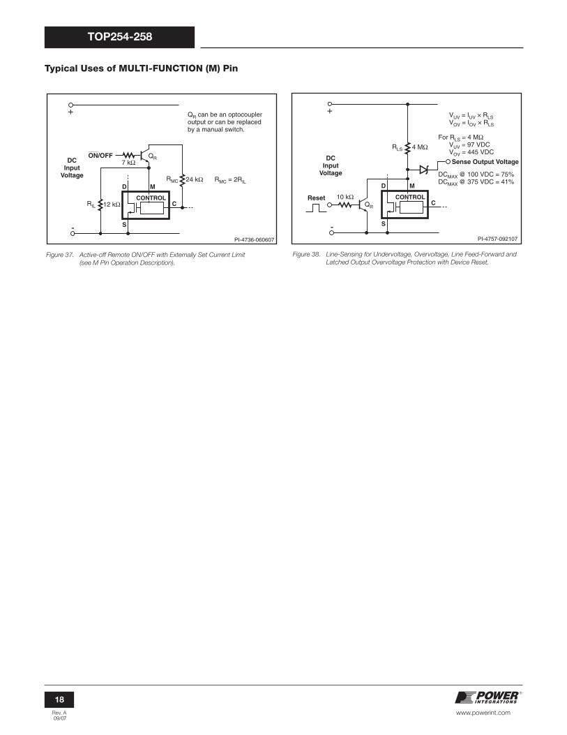
TOP254-258
TOPSwitch-HX Family
www.powerint.com September 2007
Enhanced EcoSmart®, Integrated Off-Line Switcher with Advanced Feature Set and Extended Power Range
®
Product Highlights
Lower System Cost, Higher Design Flexibility
Multi-mode operation maximizes effi ciency at all loads
No heatsink required up to 35 W using P, G and M packages
with universal input voltage and up to 48 W at 230 VAC
Output overvoltage protection (OVP) is user programmable for
latching/non-latching shutdown with fast AC reset
Allows both primary and secondary sensing
Line undervoltage (UV) detection prevents turn-off glitches
Line overvoltage (OV) shutdown extends line surge limit
Accurate programmable current limit
Optimized line feed-forward for line ripple rejection
132 kHz frequency (Y package) reduces transformer and power
supply size
Half frequency option in Y package for video applications
Tight I2f parameter tolerance reduces system cost
Maximizes MOSFET and transformer power delivery
Minimizes overload power, reducing cost of transformer,
primary clamp and secondary components
Frequency jittering reduces EMI fi lter cost
Improved auto-restart delivers <3% of maximum power in short
circuit and open loop fault conditions
Accurate hysteretic thermal shutdown function automatically
recovers without requiring a reset
Fully integrated soft-start for minimum start-up stress
Pin-out simplifi es heatsinking to the PCB for P, G and M packages
Extended creepage between DRAIN and all other pins improves
fi eld reliability
Heatsink is connected to SOURCE for low EMI
EcoSmart®– Energy Effi cient
•
•
•
•
•
•
•
•
•
•
•
•
•
•
•
•
•
•
•
•
Figure 1. Typical Flyback Application.
Energy effi cient over entire load range
No-load consumption <200 mW at 265 VAC
Standby power for 1 W input
>600 mW output at 110 VAC input
>500 mW output at 265 VAC input
Description
TOPSwitch-HX cost effectively incorporates a 700 V power
MOSFET, high voltage switched current source, PWM control,
oscillator, thermal shutdown circuit, fault protection and other
control circuitry onto a monolithic device.
•
•
•
•
•
PI-4510-100206
AC IN
DC OUT
D
S
C TOPSwitch-HX CONTROL
V
+
-
F X
Output Power Table
Product5
230 VAC ±15%4 85-265 VAC
Product5
230 VAC ±15% 85-265 VAC
Adapter1 Open
Frame2 Peak3 Adapter1 Open
Frame2 Peak3 Adapter1 Open
Frame2 Adapter1 Open
Frame2
TOP254P/GN16 W 28 W
47 W11 W 20 W
30 WTOP254YN 30 W 62 W 20 W 43 W
TOP254MN 62 W 40 W
TOP255P/GN19 W 30 W
54 W13 W 22 W
35 WTOP255YN 40 W 81 W 26 W 57 W
TOP255MN 81 W 52 W
TOP256P/GN21 W 34 W
63 W15 W 26 W
40 WTOP256YN 60 W 119 W 40 W 86 W
TOP256MN 98 W 64 W
TOP257P/GN25 W 41 W
70 W19 W 30 W
45 WTOP257YN 85 W 157 W 55 W 119 W
TOP257MN 119 W 78 W
TOP258P/GN29 W 48 W
77 W22 W 35 W
50 WTOP258YN 105 W 195 W 70 W 148 W
TOP258MN 140 W 92 W
Table 1. Output Power Table.
Notes:
1. Minimum continuous power in a typical non-ventilated enclosed adapter measured 3. Peak power capability in any design at +50 °C ambient.
at +50 °C ambient. Use of an external heat sink will increase power capability. 4. 230 VAC or 110/115 VAC with doubler.
2. Minimum continuous power in an open frame design at +50 °C ambient. 5. Packages: P: DIP-8C, G: SMD-8C, M: SDIP-10C, Y: TO-220-7C. See part
ordering information.

Rev. A 09/07
2
TOP254-258
www.powerint.com
Figure 2a. Functional Block Diagram (P and G Packages).
Figure 2b. Functional Block Diagram (M Package).
PI-4508-082907
SHUTDOWN/ AUTO-RESTART
CLOCK
CONTROLLED TURN-ON
GATE DRIVER
CURRENT LIMIT COMPARATOR
INTERNAL UV COMPARATOR
INTERNAL SUPPLY
5.8 V 4.8 V
KPS(UPPER)
KPS(LOWER)
SOURCE (S)
SOURCE (S)
S
R
Q
DMAX
STOP SOFT START
CONTROL (C)
MULTI- FUNCTION (M)
-
+ 5.8 V
IFB
ZC
VC
+
-
+
-
+
-
LEADING EDGE
BLANKING
÷ 16
1
HYSTERETIC THERMAL
SHUTDOWN
SHUNT REGULATOR/ ERROR AMPLIFIER +
-
DRAIN (D)
ON/OFF
DCMAX
DCMAX
0
OV/ UV
OVP V
VI (LIMIT) CURRENT
LIMIT ADJUST
VBG + VT
LINE SENSE
SOFT START
SOFT START IFB
IPS(UPPER) IPS(LOWER)
KPS(UPPER)KPS(LOWER)
OFF
F REDUCTION
F REDUCTION
STOP LOGIC
OSCILLATOR WITH JITTER
PWM
PI-4643-082907
SHUTDOWN/ AUTO-RESTART
CLOCK
CONTROLLED TURN-ON
GATE DRIVER
CURRENT LIMIT COMPARATOR
INTERNAL UV COMPARATOR
INTERNAL SUPPLY
5.8 V 4.8 V
SOURCE (S)
SOURCE (S)
S
R
Q
DMAX
STOP SOFT START
CONTROL (C)
VOLTAGE MONITOR (V)
-
+ 5.8 V
IFB
1 V
ZC
VC
+
-
+
-
+
-
LEADING EDGE
BLANKING
÷ 16
1
HYSTERETIC THERMAL
SHUTDOWN
SHUNT REGULATOR/ ERROR AMPLIFIER +
-
DRAIN (D)
ON/OFF
DCMAX
DCMAX
0
OV/ UV
OVP V
VI (LIMIT) CURRENT
LIMIT ADJUST
VBG + VT
LINE SENSE
SOFT START
OFF
F REDUCTION
F REDUCTION
STOP LOGIC
EXTERNAL CURRENT LIMIT (X)
OSCILLATOR WITH JITTER
PWM
KPS(UPPER)
KPS(LOWER)
SOFT START IFB
IPS(UPPER) IPS(LOWER)
KPS(UPPER)KPS(LOWER)

Rev. A 09/07
3
TOP254-258
www.powerint.com
Figure 2c. Functional Block Diagram (Y Package).
PI-4511-082907
SHUTDOWN/ AUTO-RESTART
CLOCK
CONTROLLED TURN-ON
GATE DRIVER
CURRENT LIMIT COMPARATOR
INTERNAL UV COMPARATOR
INTERNAL SUPPLY
5.8 V 4.8 V
SOURCE (S)
SOURCE (S)
S
R
Q
DMAX
STOP SOFT START
CONTROL (C)
VOLTAGE MONITOR (V)
FREQUENCY (F)
-
+ 5.8 V
IFB
1 V
ZC
VC
+
-
+
-
+
-
LEADING EDGE
BLANKING
÷ 16
1
HYSTERETIC THERMAL
SHUTDOWN
SHUNT REGULATOR/ ERROR AMPLIFIER +
-
DRAIN (D)
ON/OFF
DCMAX
DCMAX
66k/132k
0
OV/ UV
OVP V
VI (LIMIT) CURRENT
LIMIT ADJUST
VBG + VT
LINE SENSE
SOFT START
OFF
F REDUCTION
F REDUCTION
STOP LOGIC
EXTERNAL CURRENT LIMIT (X)
OSCILLATOR WITH JITTER
PWM
KPS(UPPER)
KPS(LOWER)
SOFT START IFB
IPS(UPPER) IPS(LOWER)
KPS(UPPER)KPS(LOWER)


Rev. A 09/07
5
TOP254-258
www.powerint.com
TOPSwitch-HX Family Functional Description
Like TOPSwitch-GX, TOPSwitch-HX is an integrated switched
mode power supply chip that converts a current at the control
input to a duty cycle at the open drain output of a high voltage
power MOSFET. During normal operation the duty cycle of the
power MOSFET decreases linearly with increasing CONTROL
pin current as shown in Figure 7.
In addition to the three terminal TOPSwitch features, such as
the high voltage start-up, the cycle-by-cycle current limiting,
loop compensation circuitry, auto-restart and thermal
shutdown, the TOPSwitch-HX incorporates many additional
functions that reduce system cost, increase power supply
performance and design fl exibility. A patented high voltage
CMOS technology allows both the high-voltage power MOSFET
and all the low voltage control circuitry to be cost effectively
integrated onto a single monolithic chip.
Three terminals, FREQUENCY, VOLTAGE-MONITOR, and
EXTERNAL CURRENT LIMIT (available in Y package), two
terminals, VOLTAGE-MONITOR and EXTERNAL CURRENT
LIMIT (available in M package) or one terminal MULTI-
FUNCTION (available in P and G package) have been used to
implement some of the new functions. These terminals can be
connected to the SOURCE pin to operate the TOPSwitch-HX in
a TOPSwitch-like three terminal mode. However, even in this
three terminal mode, the TOPSwitch-HX offers many
transparent features that do not require any external
components:
A fully integrated 17 ms soft-start signifi cantly reduces or
eliminates output overshoot in most applications by sweeping
both current limit and frequency from low to high to limit the
peak currents and voltages during start-up.
A maximum duty cycle (DCMAX
) of 78% allows smaller input
storage capacitor, lower input voltage requirement and/or
higher power capability.
Multi-mode operation optimizes and improves the power
supply effi ciency over the entire load range while maintaining
good cross regulation in multi-output supplies.
Switching frequency of 132 kHz reduces the transformer size
with no noticeable impact on EMI.
Frequency jittering reduces EMI in the full frequency mode at
high load condition.
Hysteretic over-temperature shutdown ensures automatic
recovery from thermal fault. Large hysteresis prevents circuit
board overheating.
Packages with omitted pins and lead forming provide large
drain creepage distance.
Reduction of the auto-restart duty cycle and frequency to
improve the protection of the power supply and load during
open loop fault, short circuit, or loss of regulation.
Tighter tolerances on I2f power coeffi cient, current limit
reduction, PWM gain and thermal shutdown threshold.
The VOLTAGE-MONITOR (V) pin is usually used for line sensing
by connecting a 4 MΩ resistor from this pin to the rectifi ed DC
high voltage bus to implement line overvoltage (OV), under-
voltage (UV) and dual-slope line feed-forward with DCMAX
1.
2.
3.
4.
5.
6.
7.
8.
9.
reduction. In this mode, the value of the resistor determines the
OV/UV thresholds and the DCMAX
is reduced linearly with a dual
slope to further improve the line ripple rejection. In addition, it
also provides another threshold to implement the latched and
hysteretic output overvoltage protection (OVP). The pin can
also be used as a remote ON/OFF using the IUV
threshold.
The EXTERNAL CURRENT LIMIT (X) pin is usually used to
reduce the current limit externally to a value close to the
operating peak current, by connecting the pin to SOURCE
through a resistor. This pin can also be used as a remote
ON/OFF input.
For the P and G package the VOLTAGE-MONITOR and
EXTERNAL CURRENT LIMIT pin functions are combined on
one MULTI-FUNCTION (M) pin. However, some of the functions
become mutually exclusive.
Figure 7. Control Pin Characteristics (Multi-Mode Operation).
PI-4645-041107
Du
ty C
ycle
(%
) D
rain
Pea
k C
urr
ent
To C
urr
ent
Lim
it R
atio
(%
) F
req
uen
cy (
kHz)
CONTROL Current
CONTROL Current
CONTROLCurrent
ICOFFIC03IC02 IC01 IB ICD1
100
78
55
25
132
66
30
Slope = PWM Gain (constant over load range)
Auto-Restart
Variable Frequency
Mode
Low Frequency
Mode
Multi-Cycle Modulation
Jitter
Full Frequency Mode


Rev. A 09/07
10
TOP254-258
www.powerint.com
Figure 10. MULTI-FUNCTION (P and G package). VOLTAGE MONITOR and EXTERNAL CURRENT LIMIT (Y and M package) Pin Characteristics.
-250 -200 -150 -100 -50 0 25 50 75 100 125 336
PI-4646-041107
Output MOSFET Switching
(Enabled)
(Disabled)
(Non-Latching) (Latching)
ILIMIT (Default)
DCMAX (78%)
Current Limit
M Pin
V Pin X Pin
Maximum Duty Cycle
VBG
I
I
I
I
IUV IREM(N) IOV IOV(LS)
Pin Voltage
Note: This figure provides idealized functional characteristics with typical performance values. Please refer to the parametric table and typical performance characteristics sections of the data sheet for measured data. For a detailed description of each functional pin operation refer to the Functional Description section of the data sheet.
X and V Pins (Y and M Packages) and M Pin (P and G Packages) Current (μA)
Disabled when supply output goes out of regulation


Rev. A 09/07
12
TOP254-258
www.powerint.com
VBG + VT
1 VVREF
240 A
400 A
CONTROL (C)
(Voltage Sense)
(Positive Current Sense - Undervoltage,Overvoltage, ON/OFF, Maximum Duty
Cycle Reduction, Output Over-voltage Protection)
(Negative Current Sense - ON/OFF,Current Limit Adjustment)
PI-4714-061207
TOPSwitch-HX
VOLTAGE MONITOR (V)
EXTERNAL CURRENT LIMIT (X)
Y and M Package
VBG + VT
VREF
240 A
400 A
CONTROL (C)
MULTI-FUNCTION (M)
(Positive Current Sense - Undervoltage,Overvoltage, Maximum Duty Cycle Reduction,
Output Overvoltage Protection)
(Negative Current Sense - ON/OFF,Current Limit Adjustment)
PI-4715-061207
TOPSwitch-HX
P and G Package
Figure 11a. VOLTAGE MONITOR (V) and EXTERNAL CURRENT LIMIT (X) Pin Input Simplifi ed Schematic.
Figure 11b. MULTI-FUNCTION (M) Pin Input Simplifi ed Schematic.

Rev. A 09/07
13
TOP254-258
www.powerint.com
Typical Uses of FREQUENCY (F) Pin
PI-2654-071700
DCInput
Voltage
+
-
D
S
CCONTROL
F
PI-2655-071700
DCInput
Voltage
+
-
D
S
CCONTROL
F
Figure 12. Full Frequency Operation (132 kHz). Figure 13. Half Frequency Operation (66 kHz).

Rev. A 09/07
14
TOP254-258
www.powerint.com
Typical Uses of VOLTAGE MONITOR (V) and EXTERNAL CURRENT LIMIT (X) Pins
X F
PI-4716-061207
DCInput
Voltage
+
-
DC S D
S
CCONTROL
V
V X C S F D
D S C
D C X V
S SS S S
PI-4717-092107
DCInput
Voltage
+
-
D
S
CCONTROL
V
4 MRLS
VUV = IUV × RLS VOV = IOV × RLS
For RLS = 4 M VUV = 97 VDC VOV = 445 VDC
DCMAX@100 VDC = 75%DCMAX@375 VDC = 41%
PI-4718-092107
DCInput
Voltage
Sense Output Voltage
+
-
D V
S
C
VUV = IUV × RLS VOV = IOV × RLS
For RLS = 4 M VUV = 97 VDC VOV = 445 VDC
DCMAX @ 100 VDC = 75%DCMAX @ 375 VDC = 41%
CONTROL
RLS 4 M
PI-4719-092107
DCInput
Voltage
Sense Output Voltage
+
-
D V
S
C
VUV = IUV × RLS VOV = IOV × RLS
For RLS = 4 M VUV = 97 VDC VOV = 445 VDC
DCMAX @ 100 VDC = 75%DCMAX @ 375 VDC = 41%
CONTROL
RLS 4 M
ROVP >3k
VROVPROVP
PI-4720-092107
DCInput
Voltage
+
-
D V
S
C
VUV = RLS × IUV
For Values Shown VUV = 98 VDCRLS
6.2 V
4 M
40 k
CONTROL
PI-4721-092107
DCInput
Voltage
+
-
D
S
CCONTROL
V
4 M
55 k
RLS
1N4148
VOV = IOV × RLS
For Values Shown VOV = 451 VDC
Figure 14. Three Terminal Operation (VOLTAGE MONITOR and EXTERNAL
CURRENT LIMIT Features Disabled. FREQUENCY Pin Tied to
SOURCE or CONTROL Pin).
Figure 15. Line-Sensing for Undervoltage, Overvoltage and Line Feed-Forward.
Figure 16. Line-Sensing for Undervoltage, Overvoltage, Line Feed-Forward and
Latched Output Overvoltage Protection.
Figure 17. Line-Sensing for Undervoltage, Overvoltage, Line Feed-Forward and
Unlatched Output Overvoltage Protection.
Figure 18. Line Sensing for Undervoltage Only (Overvoltage Disabled). Figure 19. Line-Sensing for Overvoltage Only (Undervoltage Disabled). Maximum
Duty Cycle Reduced at Low Line and Further Reduction with
Increasing Line Voltage.

Rev. A 09/07
15
TOP254-258
www.powerint.com
Typical Uses of VOLTAGE MONITOR (V) and EXTERNAL CURRENT LIMIT (X) Pins
Figure 20. External Set Current Limit.
X
PI-4722-092107
DCInput
Voltage
+
-
D
S
C
RIL
For RIL = 12 k ILIMIT = 61%
See Figure 50b for other resistor values (RIL).
For RIL = 19 k ILIMIT = 37%
CONTROL
X
PI-4723-092107
DCInput
Voltage
+
-
D
S
C
2.5 MRLS
6 kRIL
100% @ 100 VDC53% @ 300 VDC
ILIMIT =ILIMIT =
CONTROL
X
PI-2625-040501
DCInput
Voltage
+
-
D
S
C
ON/OFF47 K
QR can be an optocoupler output or can be replaced by a manual switch.
QR
CONTROL
X
ON/OFF16 k
PI-4725-060607
DCInput
Voltage
+
-
D
S
CCONTROL
V
RIL
RLS
QR
4 M
VUV = IUV × RLS VOV = IOV × RLS
DCMAX@100 VDC = 75%DCMAX@375 VDC = 41%
12 kFor RIL = ILIMIT = 61%
QR can be an optocoupler output or can be replaced by a manual switch.
X
ON/OFF16 k
PI-4724-092107
DCInput
Voltage
+
-
D
S
C
RIL QR
12 kFor RIL =
ILIMIT = 61%
19 kFor RIL =
ILIMIT = 37%
QR can be an optocoupler output or can be replaced by a manual switch.
CONTROL
X
PI-
4726
-092
107
DCInput
Voltage
+
-
D
S
CCONTROL
V
RIL
RLS
12 k
4 M
VUV = IUV x RLS VOV = IOV x RLS
For RLS = 4 M
DCMAX @ 100 VDC = 75%DCMAX @ 375 VDC = 41%
For RIL = 12 k ILIMIT = 61%
See Figure 50b for other resistor values (RIL) to select different ILIMIT values.
VUV = 97 VDC VOV = 445 VDC
Figure 21. Current Limit Reduction with Line Voltage.
Figure 22. Active-on (Fail Safe) Remote ON/OFF. Figure 23. Active-on Remote ON/OFF with Externally Set Current Limit.
Figure 24. Active-on Remote ON/OFF with LINE-SENSE and EXTERNAL
CURRENT LIMIT.
Figure 25. Line Sensing and Externally Set Current Limit.

Rev. A 09/07
16
TOP254-258
www.powerint.com
Typical Uses of VOLTAGE MONITOR (V) and EXTERNAL CURRENT LIMIT (X) Pins
PI-4727-061207
DCInput
Voltage
+
-
D
S
CCONTROL
M
D
S SS
D S C
S
CM
PI-4728-092107
DCInput
Voltage
+
-
D M
S
C
VUV = IUV × RLS VOV = IOV × RLS
For RLS = 4 M VUV = 97 VDC VOV = 445 VDC
DCMAX @ 100 VDC = 75%DCMAX @ 375 VDC = 41%
CONTROL
RLS 4 M
PI-4729-092107
DCInput
Voltage
Sense Output Voltage
+
-
D M
S
C
VUV = IUV × RLS VOV = IOV × RLS
For RLS = 4 M VUV = 97 VDC VOV = 445 VDC
DCMAX @ 100 VDC = 75%DCMAX @ 375 VDC = 41%
CONTROL
RLS 4 M
PI-4730-092107
DCInput
Voltage
Sense Output Voltage
+
-
D M
S
C
VUV = IUV × RLS VOV = IOV × RLS
For RLS = 4 M VUV = 97 VDC VOV = 445 VDC
DCMAX @ 100 VDC = 75%DCMAX @ 375 VDC = 41%
CONTROL
RLS 4 M
VROVPROVP
ROVP >3k
Figure 27. Three Terminal Operation (MULTI-FUNCTION Features Disabled). Figure 28. Line Sensing for Undervoltage, Overvoltage and Line Feed-Forward.
Figure 29. Line Sensing for Undervoltage, Overvoltage, Line Feed-Forward and
Latched Output Overvoltage Protection.
Figure 30. Line Sensing for Undervoltage, Overvoltage, Line Feed-Forward and
Unlatched Output Overvoltage Protection.
Figure 26. Line-Sensing for Undervoltage, Overvoltage, Line Feed-Forward and
Latched Output Overvoltage Protection with Device Reset.
PI-4756-092107
DCInput
Voltage
Sense Output Voltage
+
-
D V
S
C
VUV = IUV × RLS VOV = IOV × RLS
For RLS = 4 M VUV = 97 VDC VOV = 445 VDC
DCMAX @ 100 VDC = 75%DCMAX @ 375 VDC = 41%
CONTROL
RLS 4 M
10 kResetQR
Typical Uses of MULTI-FUNCTION (M) Pin

Rev. A 09/07
17
TOP254-258
www.powerint.com
PI-4731-092107
DCInput
Voltage
+
-
D M
S
C
VUV = RLS × IUV
For Values Shown VUV = 98 VDCRLS
6.2 V
4 M
40 k
CONTROL
PI-4732-092107
DCInput
Voltage
+
-
D M
S
C
VOV = IOV × RLS
For Values Shown VOV = 451 VDC
CONTROL
RLS
1N4148
4 M
55 k
Figure 31. Line Sensing for Undervoltage Only (Overvoltage Disabled). Figure 32. Line Sensing for Overvoltage Only (Undervoltage Disabled). Maximum
Duty Cycle Reduced at Low Line and Further Reduction with
Increasing Line Voltage.
Typical Uses of MULTI-FUNCTION (M) Pin
Figure 33. Externally Set Current Limit (Not Normally Required – See M Pin
Operation Description).
PI-4733-092107
DCInput
Voltage
+
-
D M
S
C
For RIL = 12 k ILIMIT = 61%
CONTROLRIL
See Figures 50b for other resistor values (RIL) to select different ILIMIT values.
For RIL = 19 k ILIMIT = 37%
PI-4734-092107
DCInput
Voltage
+
-
D M
S
CCONTROLRIL
RLS 2.5 M
6 k
100% @ 100 VDC53% @ 300 VDC
ILIMIT =ILIMIT =
PI-2519-040501
DCInput
Voltage
+
-
D
S
CQR
ON/OFF
M
CONTROL
QR can be an optocoupler output or can be replaced by a manual switch.
47 k
Figure 34. Current Limit Reduction with Line Voltage (Not Normally Required –
See M Pin Operation Description).
Figure 35. Active-on (Fail Safe) Remote ON/OFF.
PI-4735-092107
DCInput
Voltage
+
-
D
S
C
QR
RILM
CONTROL
12 kFor RIL =
ILIMIT = 61%
QR can be an optocoupler output or can be replaced by a manual switch.
ON/OFF16 k
19 kFor RIL =
ILIMIT = 37%
Figure 36. Active-on Remote ON/OFF with Externally Set Current Limit
(see M Pin Operation Description).
Rev. A 09/07
18
TOP254-258
www.powerint.com
Typical Uses of MULTI-FUNCTION (M) Pin
PI-4757-092107
DCInput
Voltage
Sense Output Voltage
+
-
D M
S
C
VUV = IUV × RLS VOV = IOV × RLS
For RLS = 4 M VUV = 97 VDC VOV = 445 VDC
DCMAX @ 100 VDC = 75%DCMAX @ 375 VDC = 41%
CONTROL
RLS 4 M
10 kQR
Reset
Figure 38. Line-Sensing for Undervoltage, Overvoltage, Line Feed-Forward and
Latched Output Overvoltage Protection with Device Reset.
PI-4736-060607
DCInput
Voltage
+
-
D
S
CRIL
RMC 24 k
12 k
M
CONTROL
QR
2RILRMC =
QR can be an optocoupler output or can be replaced by a manual switch.
ON/OFF7 k
Figure 37. Active-off Remote ON/OFF with Externally Set Current Limit
(see M Pin Operation Description).


Rev. A 09/07
25
TOP254-258
www.powerint.com
Figure 43. Layout Considerations for TOPSwitch-HX Using P-Package.
Figure 44. Layout Considerations for TOPSwitch-HX Using M-Package.
+- DCOut
+
-
HV
PI-4753-070307
Y1-Capacitor
C6
Isolation Barrier
OutputRectifier
R1 R2
JP1
J1
C1U1
R3
C2R4
D1
VR
1
C4C3
R8
D2
VR2
C5
C9
D3C7
L1
C8
J2
R8
R13
R14R6
R7
JP2
R12
R11
R10U3
R9C10
T1
Output FilterCapacitor
Input FilterCapacitor
Maximize hatched copper areas ( ) for optimum heat sinking
U2
Transformer
DSS
SS
CM
Optional PCB slot for external heatsink in contact with
SOURCE pins
+- DCOut
+
-HV
PI-4752-070307
Isolation Barrier
OutputRectifier
R1
JP1
J1
C1U1
R5
C2
R6
D1
VR
1
C4R7
C3R8
R9D2
C5
D3
C7
L1
C8
J2R11R
10
JP2
C9
R15
U3
R16
R17
R14
R12
T1
R13
VR2
R2
R3 R4
Output FilterCapacitor
Input FilterCapacitor
Optional PCB slot for external heatsink in contact with
SOURCE pins
Maximize hatched copper areas ( ) for optimum heat sinking
SS D
CXV
SSS
U2
Y1-Capacitor
C6
Transformer

Rev. A 09/07
26
TOP254-258
www.powerint.com
Figure 45. Layout Considerations for TOPSwitch-HX Using Y-Package.
clamp network, bias winding return or power traces from other
converters. If the line sensing features are used then the sense
resistors must be placed within 10 mm of the V-pin to minimize
the V pin node area. The DC bus should then be routed to the
line sense resistors. Note that external capacitance must not
be connected to the V-pin as this may cause misoperaton of the
V pin related functions.
As with any power supply design, all TOPSwitch-HX designs
should be verifi ed on the bench to make sure that components
specifi cations are not exceeded under worst-case conditions.
The following minimum set of tests is strongly recommended:
Maximum drain voltage – Verify that peak VDS
does not
exceed 675 V at highest input voltage and maximum
overload output power. Maximum overload output power
occurs when the output is overloaded to a level just before
the power supply goes into auto-restart (loss of regulation).
Maximum drain current – At maximum ambient temperature,
maximum input voltage and maximum output load, verify
drain current waveforms at start-up for any signs of trans-
former saturation and excessive leading edge current spikes.
TOPSwitch-HX has a leading edge blanking time of 220 ns
to prevent premature termination of the ON-cycle. Verify that
the leading edge current spike is below the allowed current
limit envelope (see Figure 48) for the drain current waveform
at the end of the 220 ns blanking period.
Thermal check – At maximum output power, minimum input
voltage and maximum ambient temperature; verify that
1.
2.
3.
temperature specifi cations are not exceeded for
TOPSwitch-HX, transformer, output diodes and output
capacitors. Enough thermal margin should be allowed for
the part-to-part variation of the RDS(ON)
of TOPSwitch-HX, as
specifi ed in the data sheet. The margin required can either
be calculated from the tolerances or it can be accounted for
by connecting an external resistance in series with the DRAIN
pin and attached to the same heat sink, having a resistance
value that is equal to the difference between the measured
RDS(ON)
of the device under test and the worst case maximum
specifi cation.
Design Tools
Up-to-date information on design tools can be found at the
Power Integrations website: www.powerint.com
+- DCOut
+
-HV
PI-4751-070307
Y1-Capacitor
C6
Isolation Barrier
OutputRectifier
R1 R2
R3 R4
JP1
J1
C1
U1HS1
R3
C2
R4
D1
VR
1C4
R7 R10R13
D2
VR2
C5 C9
D3
C7
L1
C8
J2R
9
R11
R16 R
14
R8
JP2
R12R17
R15
U3
R12
C10
T1
Output FilterCapacitor
Input FilterCapacitor
Transformer
S F
C
X V
D
U2

Rev. A 09/07
27
TOP254-258
www.powerint.com
Absolute Maximum Ratings(2)
DRAIN Peak Voltage .................................................................. -0.3 V to 700 V
DRAIN Peak Current: TOP254 ................................................................ 2.08 A
DRAIN Peak Current: TOP255 .................................................................2.72 A
DRAIN Peak Current: TOP256 ................................................................ 4.08 A
DRAIN Peak Current: TOP257 ................................................................ 5.44 A
DRAIN Peak Current: TOP258 ................................................................ 6.88 A
CONTROL Voltage ............................................................................-0.3 V to 9 V
CONTROL Current ...................................................................................... 100 mA
VOLTAGE MONITOR Pin Voltage .............................................-0.3 V to 9 V
CURRENT LIMIT Pin Voltage .................................................-0.3 V to 4.5 V
MULTI-FUNCTION Pin Voltage .................................................-0.3 V to 9 V
FREQUENCY Pin Voltage ........................................................... -0.3 V to 9 V
Storage Temperature ............................................................ -65 °C to 150 °C
Operating Junction Temperature ................................... -40 °C to 150 °C
Lead Temperature(1) ......................................................................................260 °C
Notes:
1. 1/16 in. from case for 5 seconds.
2. Maximum ratings specifi ed may be applied one at a time
without causing permanent damage to the product. Exposure
to Absolute Maximum Rating conditions for extended periods
of time may affect product reliability.
Thermal Impedance
Thermal Impedance: Y Package:
(θJA
) .................................................................. 80 °C/W(1)
(θJC
) ............................................... .....................2 °C/W(2)
P, G and M Packages: (θ
JA) .........................................70 °C/W(3); 60 °C/W(4)
(θJC
) ............................................... ..................11 °C/W(5)
Notes:
1. Free standing with no heatsink.
2. Measured at the back surface of tab.
3. Soldered to 0.36 sq. in. (232 mm2), 2 oz. (610 g/m2) copper clad.
4. Soldered to 1 sq. in. (645 mm2), 2 oz. (610 g/m2) copper clad.
5. Measured on the SOURCE pin close to plastic interface.
Parameter Symbol
Conditions
SOURCE = 0 V; TJ = -40 to 125 °C
See Figure 49
(Unless Otherwise Specifi ed)
Min Typ Max Units
Control Functions
Switching Frequency
in Full Frequency
Mode (average)
fOSC
TJ = 25 °C
FREQUENCY Pin Connected to SOURCE
119 132 145
kHzFREQUENCY Pin Connected to CONTROL 59.5 66 72.5
M/P/G Package
Frequency Jitter
DeviationΔf
132 kHz Operation ±5kHz
66 kHz Operation ±2.5
Frequency Jitter
Modulation RatefM
250 Hz
Maximum Duty Cycle DCMAX
IC = I
CD1
IV ≤ I
V(DC) or I
M ≤ I
M(DC) or
VV, V
M = 0 V
75 78 83
%
IV or I
M = 95 μA 30
Soft-Start Time tSOFT
TJ = 25 °C 17 ms
PWM Gain DCreg
TJ = 25 °C
TOP254-255 -30 -25 -20%/mA
TOP256-258 -27 -22 -17
PWM Gain
Temperature DriftSee Note A -0.01 %/mA/°C
External Bias Current IB
66 kHz OperationTOP254-255 0.9 1.5 2.1
mATOP256-258 1.0 1.6 2.2
132 kHz OperationTOP254-255 1.0 1.6 2.2
TOP256-258 1.3 1.9 2.5

Rev. A 09/07
28
TOP254-258
www.powerint.com
Parameter Symbol
Conditions
SOURCE = 0 V; TJ = -40 to 125 °C
(Unless Otherwise Specifi ed)
Min Typ Max Units
Control Functions (cont.)
CONTROL Current at
0% Duty CycleIC(OFF)
66 kHz OperationTOP254-255 4.4 5.8
mATOP256-258 4.7 6.1
132 kHz OperationTOP254-255 4.6 6.0
TOP256-258 5.1 6.5
Dynamic
ImpedanceZ
CIC = 4 mA; T
J = 25 °C, See Figure 47 10 15 22 Ω
Dynamic Impedance
Temperature Drift0.18 %/°C
CONTROL Pin Internal
Filter Pole7 kHz
Upper Peak Current to
Set Current Limit Ratiok
PS(UPPER)T
J = 25 °C 50 55 60 %
Lower Peak Current to
Set Current Limit Ratiok
PS(LOWER)T
J = 25 °C 25 %
Multi-Cycle-
Modulation Switching
Frequency
fMCM(MIN)
TJ = 25 °C 30 kHz
Minimum Multi-Cycle-
Modulation On PeriodT
MCM(MIN)T
J = 25 °C 135 μs
Shutdown/Auto-Restart
Control Pin
Charging CurrentIC(CH)
TJ = 25 °C
VC = 0 V -5.0 -3.5 -1.0
mAV
C = 5 V -3.0 -1.8 -0.6
Charging Current
Temperature DriftSee Note A 0.5 %/°C
Auto-Restart
Upper Threshold
Voltage
VC(AR)U
5.8 V
Auto-Restart Lower
Threshold VoltageV
C(AR)L4.5 4.8 5.1 V
Multi-Function (M), Voltage Monitor (V) and External Current Limit (X) Inputs
Auto-Restart
Hysteresis VoltageV
C(AR)hyst0.8 1.0 V
Auto-Restart Duty
CycleDC
(AR)2 4 %
Auto-Restart
Frequencyf(AR)
0.5 Hz
Line Undervoltage
Threshold Current and
Hysteresis (M or V Pin)
IUV
TJ = 25 °C
Threshold 22 25 27 μA
Hysteresis 14 μA
Line Overvoltage
Threshold Current and
Hysteresis (M or V Pin)
IOV
TJ = 25 °C
Threshold 107 112 117 μA
Hysteresis 4 μA
Output Overvoltage
Latching Shutdown
Threshold Current
IOV(LS)
TJ = 25 °C 269 336 403 μA

Rev. A 09/07
29
TOP254-258
www.powerint.com
Parameter Symbol
ConditionsSOURCE = 0 V; T
J = -40 to 125 °C
(Unless Otherwise Specifi ed)
Min Typ Max Units
Multi-Function (M), Voltage Monitor (V) and External Current Limit (X) Inputs
V or M Pin Reset Voltage V
V(TH) or
VM(TH)
TJ = 25 °C 0.8 1.0 1.6 V
Remote ON/OFF
Negative Threshold
Current and Hysteresis
(M or X Pin)
IREM (N)
TJ = 25 °C
Threshold -35 -27 -20
μA
Hysteresis 5
V or M Pin Short Circuit
Current
IV(SC)
or
IM(SC)
TJ = 25 °C V
V, V
M = V
C300 400 500 μA
X or M Pin Short Circuit
Current
IX(SC)
or
IM(SC)
VX, V
M = 0 V
Normal Mode -260 -200 -140μA
Auto-Restart Mode -95 -75 -55
V or M Pin Voltage
(Positive Current)V
V or
V
M
IV or I
M = I
UV2.10 2.8 3.20
VIV or I
M = I
OV2.79 3.0 3.21
V or M Pin Voltage
Hysteresis (Positive
Current)
VV(hyst)
or
VM(hyst)
IV or I
M = I
OV0.2 0.5 V
X or M Pin Voltage
(Negative Current)V
X or V
M
IX or I
M = -50 μA 1.23 1.30 1.37
VIX or I
M = -150 μA 1.15 1.22 1.29
Maximum Duty Cycle
Reduction Onset
Threshold Current
IV(DC)
or
IM(DC)
IC ≥ I
B, T
J = 25 °C 18.9 22.0 24.2 μA
Maximum Duty Cycle
Reduction SlopeT
J = 25 °C
IV(DC)
< IV <48 μA or
IM(DC)
< IM
<48 μA-1.0
%/μA
IV or I
M ≥48 μA -0.25
Remote OFF DRAIN
Supply CurrentID(RMT)
VDRAIN
= 150 V
X, V or M Pin
Floating0.6 1.0
mAV or M Pin Shorted to
CONTROL1.0 1.6
Remote ON Delay tR(ON)
From Remote ON to Drain
Turn-On
See Note B
66 kHz 3.0
μs132 kHz 1.5
Remote OFF Setup Time tR(OFF)
Minimum Time Before Drain
Turn-On to Disable Cycle
See Note B
66 kHz 3.0
μs132 kHz 1.5
Frequency Input
FREQUENCY Pin
Threshold VoltageV
FSee Note B 2.9 V
FREQUENCY Pin Input
CurrentIF
VF = V
C10 55 100 μA
Rev. A 09/07
30
TOP254-258
www.powerint.com
Parameter Symbol
ConditionsSOURCE = 0 V; T
J = -40 to 125 °C
(Unless Otherwise Specifi ed)
Min Typ Max Units
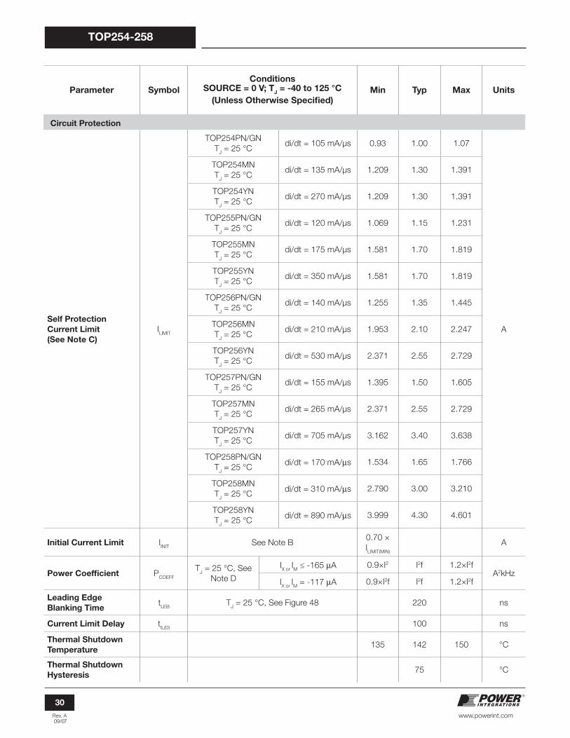
Circuit Protection
Self Protection
Current Limit
(See Note C)
ILIMIT
TOP254PN/GN
TJ = 25 °C
di/dt = 105 mA/μs 0.93 1.00 1.07
A
TOP254MN
TJ = 25 °C
di/dt = 135 mA/μs 1.209 1.30 1.391
TOP254YN
TJ = 25 °C
di/dt = 270 mA/μs 1.209 1.30 1.391
TOP255PN/GN
TJ = 25 °C
di/dt = 120 mA/μs 1.069 1.15 1.231
TOP255MN
TJ = 25 °C
di/dt = 175 mA/μs 1.581 1.70 1.819
TOP255YN
TJ = 25 °C
di/dt = 350 mA/μs 1.581 1.70 1.819
TOP256PN/GN
TJ = 25 °C
di/dt = 140 mA/μs 1.255 1.35 1.445
TOP256MN
TJ = 25 °C
di/dt = 210 mA/μs 1.953 2.10 2.247
TOP256YN
TJ = 25 °C
di/dt = 530 mA/μs 2.371 2.55 2.729
TOP257PN/GN
TJ = 25 °C
di/dt = 155 mA/μs 1.395 1.50 1.605
TOP257MN
TJ = 25 °C
di/dt = 265 mA/μs 2.371 2.55 2.729
TOP257YN
TJ = 25 °C
di/dt = 705 mA/μs 3.162 3.40 3.638
TOP258PN/GN
TJ = 25 °C
di/dt = 170 mA/μs 1.534 1.65 1.766
TOP258MN
TJ = 25 °C
di/dt = 310 mA/μs 2.790 3.00 3.210
TOP258YN
TJ = 25 °C
di/dt = 890 mA/μs 3.999 4.30 4.601
Initial Current Limit IINIT
See Note B0.70 ×
ILIMIT(MIN)
A
Power Coeffi cient PCOEFF
TJ = 25 °C, See
Note D
IX or
IM ≤ -165 μA 0.9×I2 I2f 1.2×I2f
A2kHzIX or
IM = -117 μA 0.9×I2f I2f 1.2×I2f
Leading Edge
Blanking TimetLEB
TJ = 25 °C, See Figure 48 220 ns
Current Limit Delay tIL(D)
100 ns
Thermal Shutdown
Temperature135 142 150 °C
Thermal Shutdown
Hysteresis75 °C

Rev. A 09/07
31
TOP254-258
www.powerint.com
Parameter Symbol
ConditionsSOURCE = 0 V; T
J = -40 to 125 °C
(Unless Otherwise Specifi ed)
Min Typ Max Units
Circuit Protection (cont.)
Power-Up Reset
Threshold VoltageV
C(RESET)Figure 47 (S1 Open Condition) 1.75 3.0 4.25 V
Output
ON-State
ResistanceR
DS(ON)
TOP254
ID = 150 mA
TJ = 25 °C 5.40 6.25
Ω
TJ = 100 °C 8.35 9.70
TOP255
ID = 200 mA
TJ = 25 °C 4.10 4.70
TJ = 100 °C 6.30 7.30
TOP256
ID = 300 mA
TJ = 25 °C 2.80 3.20
TJ = 100 °C 4.10 4.75
TOP257
ID = 400 mA
TJ = 25 °C 2.00 2.30
TJ = 100 °C 3.10 3.60
TOP258
ID = 500 mA
TJ = 25 °C 1.70 1.95
TJ = 100 °C 2.50 2.90
DRAIN Supply VoltageT
J

Rev. A 09/07
32
TOP254-258
www.powerint.com
NOTES:
For specifi cations with negative values, a negative temperature coeffi cient corresponds to an increase in
magnitude with increasing temperature, and a positive temperature coeffi cient corresponds to a decrease in
magnitude with increasing temperature.
Guaranteed by characterization. Not tested in production.
For externally adjusted current limit values, please refer to Figures 50a and 50b (Current Limit vs. External Current Limit Resis-
tance) in the Typical Performance Characteristics section. The tolerance specifi ed is only valid at full current limit.
I2f calculation is based on typical values of ILIMIT
and fOSC,
i.e. ILIMIT(TYP)
2 × fOSC(66K, TYP)
, where fOSC(66K, TYP)
= 66 kHz / 132 kHz depending
on package / F pin connection. See fOSC
specifi cation for detail.
The TOPSwitch-HX will start up at 18 VDC
Drain voltage. The capacitance of electrolytic capacitors drops signifi cantly at tempera-
tures below 0 °C. For reliable start up at 18 V in sub zero temperatures, designers must ensure that circuit capacitors meet
recommended capacitance values.
A.
B.
C.
D.
E.

Rev. A 09/07
33
TOP254-258
www.powerint.com
Figure 46. Duty Cycle Measurement.
Figure 47. CONTROL Pin I-V Characteristic. Figure 48. Drain Current Operating Envelope.
Figure 49. TOPSwitch-HX General Test Circuit.
PI-2039-033001
DRAINVOLTAGE
HV
0 V
90%
10%
90%

Rev. A 09/07
34
TOP254-258
www.powerint.com
Figure 50a. Normalized Current Limit vs. X or M Pin Current.
Figure 50b. Normalized Current Limit vs. External Current Limit Resistance.
PI-4754-082907
0
0.1
0.2
0.3
0.4
0.5
0.6
0.7
0.8
0.9
1
1.1
-200 -150 -100 -50 0
IX or IM ( μA )
0
0.1
0.2
0.3
0.4
0.5
0.6
0.7
0.8
0.9
1
1.1
Typical
Notes:1. Maximum and Minimum levels are based on characterization;
2. T J = 0 OC to 125 OC
Minimum
Maximum
Nor
mal
ized
Cur
rent
Lim
it
Nor
mal
ized
di/d
t
PI-4755-082907
0
0.1
0.2
0.3
0.4
0.5
0.6
0.7
0.8
0.9
1
1.1
0 5 10 15 20 25 30 35 40 45
RIL ( kΩ )
0
0.1
0.2
0.3
0.4
0.5
0.6
0.7
0.8
0.9
1
1.1Notes:1. Maximum and Minimum levels are based on characterization;
2. T J = 0 OC to 125 OC;3. Includes the variation of X or M pin voltage
Typical
Maximum
Minimum
Norm
aliz
ed C
urre
nt L
imit
Norm
aliz
ed d
i/dt
Typical Performance Characteristics

Rev. A 09/07
35
TOP254-258
www.powerint.com
Typical Performance Characteristics
1.1
1.0
0.9-50 -25 0 25 50 75 100 125 150
Junction Temperature ( C)
Bre
akd
ow
n V
olt
age
(No
rmal
ized
to
25
C) PI-
176B
-033
001 1.2
1.0
0.8
0.6
0.4
0.2
0-50 -25 0 25 50 75 100 125 150
Junction Temperature ( C)
PI-
4759
-061
407
Ou
tpu
t F
req
uen
cy(N
orm
aliz
ed t
o 2
5 C
)
1.2
1.0
0.8
0.6
0.4
0.2
0-50 -25 0 25 50 75 100 125 150
Junction Temperature ( C)
PI-
4760
-061
407
Cu
rren
t L
imit
(No
rmal
ized
to
25
C)
1.2
1.0
0.8
0.6
0.4
0.2
0-50 -25 0 25 50 75 100 125 150
Junction Temperature (°C)
PI-
4739
-061
507
Cu
rren
t L
imit
(No
rmal
ized
to
25
°C)
1.2
1.0
0.8
0.6
0.4
0.2
0-50 -25 0 25 50 75 100 125 150
Junction Temperature ( C)
PI-
4761
-061
407
Ove
rvo
ltag
e T
hre
sho
ld(N
orm
aliz
ed t
o 2
5 C
)
1.2
1.0
0.8
0.6
0.4
0.2
0-50 -25 0 25 50 75 100 125 150
Junction Temperature ( C)
PI-
4762
-061
407
Un
der
-Vo
ltag
e T
hre
sho
ld(N
orm
aliz
ed t
o 2
5 C
)
Figure 51. Breakdown Voltage vs. Temperature. Figure 52. Frequency vs. Temperature.
Figure 53. Internal Current Limit vs. Temperature. Figure 54. External Current Limit vs. Temperature with RIL = 10.5 kΩ.
Figure 55. Overvoltage Threshold vs. Temperature. Figure 56. Undervoltage Threshold vs. Temperature.

Rev. A 09/07
36
TOP254-258
www.powerint.com
Typical Performance Characteristics
6
4.5
5.5
5
20 100 200 500400300
VOLTAGE-MONITOR Pin Current ( A)
VO
LTA
GE
MO
NIT
OR
Pin
Vo
ltag
e (V
)
PI-
4740
-060
607
3
2.5
3.5
4
1.6
1.0
1.4
1.2
0200 -150 -50-100 0
EXTERNAL CURRENT LIMIT Pin Current ( A)
EX
TE
RN
AL
CU
RR
EN
T L
IMIT
P
in V
olt
age
(V)
PI-
4741
-061
407
0.4
0.2
0.6
0.8
VX = 1.354 - 1147.5 × IX 1.759 × 10⁶ × (IX)2 with -180 A IX -25 A
6
5
4
3
2
1
0-200 -100 0 100 200 300 400 500
PI-
4742
-061
207
MU
LTI-
FU
NC
TIO
N P
in V
olt
age
(V)
MULTI-FUNCTION Pin Current ( A)
See expandedversion(Figure 58b)
1.2
1.4
1.6
0.4
0.6
0.2
0.8
1.0
0-200 -150 -50-100 0
MU
LTI-
FU
NC
TIO
N P
in V
olt
age
(V)
PI-
4743
-061
407
MULTI-FUNCTION Pin Current ( A)
VM = 1.354 - 1147.5 × IM 1.759 × 10⁶ × (IM)2 with -180 A IM -25 A
1.2
1.0
0.8
0.6
0.4
0.2
0-50 -25 0 25 50 75 100 125 150
Junction Temperature ( C)
PI-
4763
-061
407
CO
NT
RO
L C
urr
ent
(No
rmal
ized
to
25
C)
1.2
1.0
0.8
0.6
0.4
0.2
0-50 -25 0 25 50 75 100 125 150
Junction Temperature ( C)
PI-
4764
-061
407
On
set
Th
resh
old
Cu
rren
t(N
orm
aliz
ed t
o 2
5 C
)
Figure 57a. LINE-SENSE Pin Voltage vs. Current. Figure 57b. EXTERNAL CURRENT LIMIT Pin Voltage vs. Current.
Figure 58a. MULTI-FUNCTION Pin Voltage vs. Current. Figure 58b. MULTI-FUNCTION Pin Voltage vs. Current (Expanded).
Figure 59. Control Current Out at 0% Duty Cycle vs. Temperature. Figure 60. Maximum Duty Cycle Reduction Onset Threshold
Current vs. Temperature.

Rev. A 09/07
37
TOP254-258
www.powerint.com
Typical Performance Characteristics
1
-0.5
0
0.5
-2.50 20 40 60 80 100
DRAIN Pin Voltage (V)
CO
NT
RO
L P
in C
urr
ent
(mA
)
PI-
4744
-061
207
-1.5
-2
-1
VC = 5 V
Figure 61. Output Characteristics. Figure 62. IC vs. DRAIN Voltage.
Figure 63. COSS
vs. DRAIN Voltage. Figure 64. DRAIN Capacitance Power.
Figure 65. Remote OFF DRAIN Supply Current vs. Temperature.
5
00 2 4 6 8 10 12 14 16 18 20
DRAIN Voltage (V)
DR
AIN
Cu
rren
t (A
) PI-
4748
-061
207
2
1
TCASE = 25 CTCASE = 100 C
4
3
TOP258 1.00TOP257 0.85TOP256 0.61TOP255 0.42TOP254 0.32
Scaling Factors:
0 100 200 300 400 500 60010
100
1000
10000
PI-
4749
-061
207
Drain Voltage (V)
DR
AIN
Cap
acit
ance
(p
F)
TOP258 1.00TOP257 0.85TOP256 0.61TOP255 0.42TOP254 0.32
Scaling Factors:500
400
200
100
300
00 200100 400 500 600300 700
DRAIN Voltage (V)
Po
wer
(m
W)
PI-
4750
-061
407
Y-Package
P/M-Package
TOP258 1.00TOP257 0.85TOP256 0.61TOP255 0.42TOP254 0.32
Scaling Factors:
1.2
0.8
1.0
0-50 0-25 5025 10075 125 150
Junction Temperature ( C)
Rem
ote
OF
F D
RA
IN S
up
ply
Cu
rren
t (
No
rmal
ized
to
25
C)
PI-
4745
-061
407
0.2
0.4
0.6

Rev. A 09/07
38
TOP254-258
www.powerint.com
PI-2644-122004
Notes:1. Controlling dimensions are inches. Millimeter dimensions are shown in parentheses. 2. Pin numbers start with Pin 1, and continue from left to right when viewed from the front.3. Dimensions do not include mold flash or other protrusions. Mold flash or protrusions shall not exceed .006 (.15mm) on any side.4. Minimum metal to metal spacing at the package body for omitted pin locations is .068 in. (1.73 mm).5. Position of terminals to be measured at a location .25 (6.35) below the package body.6. All terminals are solder plated.
Y07C
PIN 1 PIN 7
MOUNTING HOLE PATTERN
.050 (1.27)
.150 (3.81)
.050 (1.27)
.150 (3.81)
.050 (1.27)
.050 (1.27)
.100 (2.54)
.180 (4.58).200 (5.08)
PIN 1
+
.010 (.25) M
.461 (11.71)
.495 (12.57)
.390 (9.91).420 (10.67).146 (3.71)
.156 (3.96)
.860 (21.84)
.880 (22.35)
.024 (.61)
.034 (.86)
.068 (1.73) MIN
.050 (1.27) BSC
.150 (3.81) BSC
.108 (2.74) REF
PIN 1 & 7
7° TYP.
PIN 2 & 4
.040 (1.02)
.060 (1.52)
.190 (4.83)
.210 (5.33)
.012 (.30)
.024 (.61)
.080 (2.03)
.120 (3.05)
.234 (5.94)
.261 (6.63)
.165 (4.19)
.185 (4.70)
.040 (1.02)
.060 (1.52)
.045 (1.14)
.055 (1.40)
.670 (17.02) REF.
.570 (14.48) REF.
TO-220-7C

Rev. A 09/07
39
TOP254-258
www.powerint.com
Notes:1. Package dimensions conform to JEDEC specification MS-001-AB (Issue B 7/85) for standard dual-in-line (DIP) package with .300 inch row spacing.2. Controlling dimensions are inches. Millimeter sizes are shown in parentheses.3. Dimensions shown do not include mold flash or other protrusions. Mold flash or protrusions shall not exceed .006 (.15) on any side.4. Pin locations start with Pin 1, and continue counter-clock- wise to Pin 8 when viewed from the top. The notch and/or dimple are aids in locating Pin 1. Pin 3 is omitted.5. Minimum metal to metal spacing at the package body for the omitted lead location is .137 inch (3.48 mm).6. Lead width measured at package body. 7. Lead spacing measured with the leads constrained to be perpendicular to plane T.
.008 (.20)
.015 (.38)
.300 (7.62) BSC(NOTE 7)
.300 (7.62)
.390 (9.91)
.367 (9.32)
.387 (9.83)
.240 (6.10)
.260 (6.60)
.125 (3.18)
.145 (3.68)
.057 (1.45)
.068 (1.73)
.120 (3.05)
.140 (3.56)
.015 (.38)MINIMUM
.048 (1.22)
.053 (1.35).100 (2.54) BSC
.014 (.36)
.022 (.56)
-E-
Pin 1
SEATINGPLANE
-D-
-T-
P08C
DIP-8C
PI-3933-100504
D S .004 (.10)⊕
T E D S .010 (.25) M⊕
(NOTE 6)
.137 (3.48)MINIMUM
Notes:1. Package dimensions conform to JEDEC specification MS-019.2. Controlling dimensions are inches. Millimeter sizes are shown in parentheses.3. Dimensions shown do not include mold flash or other protrusions. Mold flash or protrusions shall not exceed .006 (.15) on any side.4. D, E and F are reference datums.5. Dimensioning and tolerancing conform to ASME Y14.5M-1994.
.008 (.20)
.015 (.38)
.300 (7.62)
.390 (9.91)
.240 (6.10)
.260 (6.60)
10 6
1 5
.200 (5.08) Max
.020 (.51) Min
.367 (9.32)
.387 (9.83)
.120 (3.05)
.140 (3.56)
.030 (.76).040 (1.02)
.070 (1.78) BSC .300 BSC
.300 (7.62).340 (8.64
.014 (.36)
.022 (.56)
.125 (3.18)
.145 (3.68)
-E-
SEATINGPLANE
-D-
P10C
SDIP-10C
PI-4648-041107
F D E.010 (.25) M⊕
-F-

Rev. A 09/07
40
TOP254-258
www.powerint.com
Part Ordering Information
• TOPSwitch Product Family
• HX Series Number
• Package Identifi er
P Plastic DIP-8C
G Plastic SMD-8C
M Plastic SDIP-10C
Y Plastic TO-220-7C
• Pin Finish
N Pure Matte Tin (Pb-Free) (P, G, M and Y Packages)
• Tape & Reel and Other Options
Blank Standard Confi gurations
TL G Package (1000 min/mult.)TOP 258 P N - TL
SMD-8C
PI-4015-013106
.004 (.10)
.012 (.30) .036 (0.91) .044 (1.12)
.004 (.10)
0 - ° 8 °
.367 (9.32)
.387 (9.83)
.048 (1.22) .009 (.23)
.053 (1.35) .032 (.81) .037 (.94)
.125 (3.18)
.145 (3.68)
-D-
Notes: 1. Controlling dimensions are inches. Millimeter sizes are shown in parentheses. 2. Dimensions shown do not include mold flash or other protrusions. Mold flash or protrusions shall not exceed .006 (.15) on any side. 3. Pin locations start with Pin 1, and continue counter-clock- wise to Pin 8 when viewed from the top. Pin 3 is omitted. 4. Minimum metal to metal spacing at the package body for the omitted lead location is .137 inch (3.48 mm). 5. Lead width measured at package body. 6. D and E are referenced datums on the package body.
.057 (1.45)
.068 (1.73) (NOTE 5)
E S
.100 (2.54) (BSC)
.372 (9.45) .240 (6.10)
.388 (9.86) .260 (6.60)
.010 (.25)
-E-
Pin 1
D S .004 (.10) ⊕
⊕
G08C
.420
.046 .060 .060 .046
.080
Pin 1
.086
.186
.286
Solder Pad Dimensions
.137 (3.48) MINIMUM

Rev. A 09/07
41
TOP254-258
www.powerint.com
Notes

For the latest updates, visit our website: www.powerint.comPower Integrations reserves the right to make changes to its products at any time to improve reliability or manufacturability. Power
Integrations does not assume any liability arising from the use of any device or circuit described herein. POWER INTEGRATIONS
MAKES NO WARRANTY HEREIN AND SPECIFICALLY DISCLAIMS ALL WARRANTIES INCLUDING, WITHOUT LIMITATION, THE
IMPLIED WARRANTIES OF MERCHANTABILITY, FITNESS FOR A PARTICULAR PURPOSE, AND NON-INFRINGEMENT OF THIRD
PARTY RIGHTS.
Patent Information
The products and applications illustrated herein (including transformer construction and circuits external to the products) may be
covered by one or more U.S. and foreign patents, or potentially by pending U.S. and foreign patent applications assigned to Power
Integrations. A complete list of Power Integrations patents may be found at www.powerint.com. Power Integrations grants its
customers a license under certain patent rights as set forth at http://www.powerint.com/ip.htm.
Life Support Policy
POWER INTEGRATIONS PRODUCTS ARE NOT AUTHORIZED FOR USE AS CRITICAL COMPONENTS IN LIFE SUPPORT
DEVICES OR SYSTEMS WITHOUT THE EXPRESS WRITTEN APPROVAL OF THE PRESIDENT OF POWER INTEGRATIONS. As
used herein:
A Life support device or system is one which, (i) is intended for surgical implant into the body, or (ii) supports or sustains life, and
(iii) whose failure to perform, when properly used in accordance with instructions for use, can be reasonably expected to result in
signifi cant injury or death to the user.
A critical component is any component of a life support device or system whose failure to perform can be reasonably expected to
cause the failure of the life support device or system, or to affect its safety or effectiveness.
The PI logo, TOPSwitch, TinySwitch, LinkSwitch, DPA-Switch, PeakSwitch, EcoSmart, Clampless, E-Shield, Filterfuse, StakFET,
PI Expert and PI FACTS are trademarks of Power Integrations, Inc. Other trademarks are property of their respective companies.
©2007, Power Integrations, Inc.
1.
2.
Power Integrations Worldwide Sales Support Locations
World Headquarters5245 Hellyer Avenue
San Jose, CA 95138, USA.
Main: +1-408-414-9200
Customer Service:
Phone: +1-408-414-9665
Fax: +1-408-414-9765
e-mail: [email protected]
China (Shanghai)Rm 807-808A
Pacheer Commercial Centre,
555 Nanjing Rd. West
Shanghai, P.R.C. 200041
Phone: +86-21-6215-5548
Fax: +86-21-6215-2468
e-mail: [email protected]
China (Shenzhen)Rm 2206-2207, Block A,
Electronics Science and
Technology Bldg.
2070 Shennan Zhong Rd.
Shenzhen, Guangdong,
China, 518031
Phone: +86-755-8379-3243
Fax: +86-755-8379-5828
e-mail: [email protected]
GermanyRueckertstrasse 3
D-80336, Munich
Germany
Phone: +49-89-5527-3911
Fax: +49-89-5527-3920
e-mail: [email protected]
India#1, 14th Main Road
Vasanthanagar
Bangalore-560052 India
Phone: +91-80-4113-8020
Fax: +91-80-4113-8023
e-mail: [email protected]
ItalyVia De Amicis 2
20091 Bresso MI
Italy
Phone: +39-028-928-6000
Fax: +39-028-928-6009
e-mail: [email protected]
JapanKosei Dai-3 Bldg.,
2-12-11, Shin-Yokohama,
Kohoku-ku, Yokohama-shi,
Kanagawa 222-0033
Phone: +81-45-471-1021
Fax: +81-45-471-3717
e-mail: [email protected]
KoreaRM 602, 6FL
Korea City Air Terminal B/D, 159-6
Samsung-Dong, Kangnam-Gu,
Seoul, 135-728, Korea
Phone: +82-2-2016-6610
Fax: +82-2-2016-6630
e-mail: [email protected]
Singapore51 Newton Road
#15-08/10 Goldhill Plaza
Singapore, 308900
Phone: +65-6358-2160
Fax: +65-6358-2015
e-mail: [email protected]
Taiwan5F, No. 318, Nei Hu Rd., Sec. 1
Nei Hu Dist.
Taipei, Taiwan 114, R.O.C.
Phone: +886-2-2659-4570
Fax: +886-2-2659-4550
e-mail: [email protected]
Europe HQ1st Floor, St. James’s House
East Street, Farnham
Surrey GU9 7TJ
United Kingdom
Phone: +44 (0) 1252-730-141
Fax: +44 (0) 1252-727-689
e-mail: [email protected]
Applications HotlineWorld Wide +1-408-414-9660
Applications FaxWorld Wide +1-408-414-9760
Revision Notes Date
A Initial Release 09/07