Embed Size (px)
Citation preview
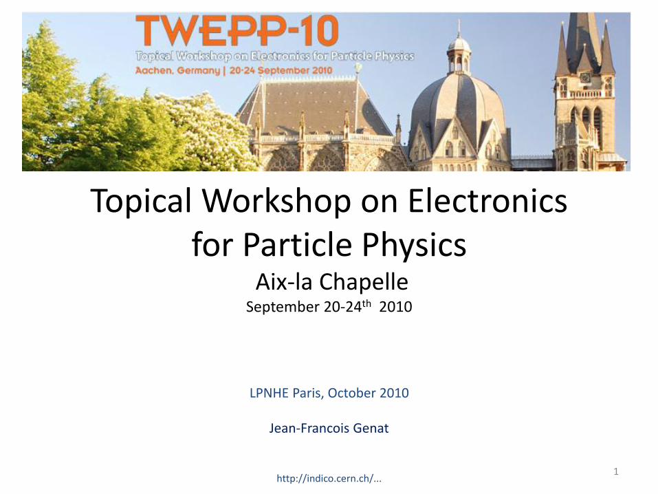
Topical Workshop on Electronics for Particle Physics
Aix-la Chapelle September 20-24th 2010
LPNHE Paris, October 2010
Jean-Francois Genat
http://indico.cern.ch/... 1
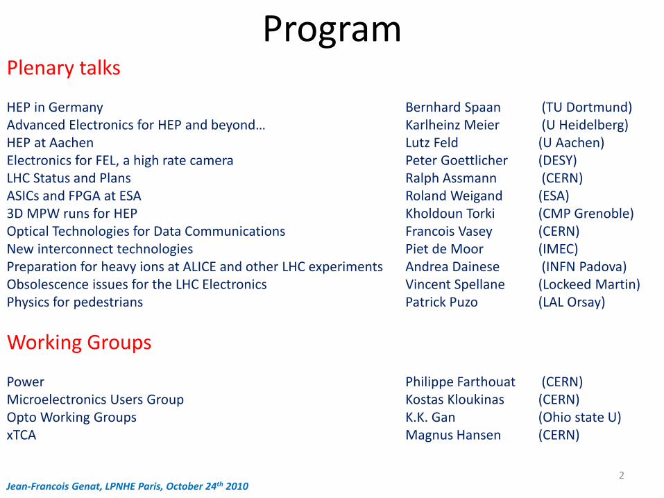
Program Plenary talks HEP in Germany Bernhard Spaan (TU Dortmund) Advanced Electronics for HEP and beyond… Karlheinz Meier (U Heidelberg) HEP at Aachen Lutz Feld (U Aachen) Electronics for FEL, a high rate camera Peter Goettlicher (DESY) LHC Status and Plans Ralph Assmann (CERN) ASICs and FPGA at ESA Roland Weigand (ESA) 3D MPW runs for HEP Kholdoun Torki (CMP Grenoble) Optical Technologies for Data Communications Francois Vasey (CERN) New interconnect technologies Piet de Moor (IMEC) Preparation for heavy ions at ALICE and other LHC experiments Andrea Dainese (INFN Padova) Obsolescence issues for the LHC Electronics Vincent Spellane (Lockeed Martin) Physics for pedestrians Patrick Puzo (LAL Orsay)
Working Groups Power Philippe Farthouat (CERN) Microelectronics Users Group Kostas Kloukinas (CERN) Opto Working Groups K.K. Gan (Ohio state U) xTCA Magnus Hansen (CERN)
Jean-Francois Genat, LPNHE Paris, October 24th 2010 2
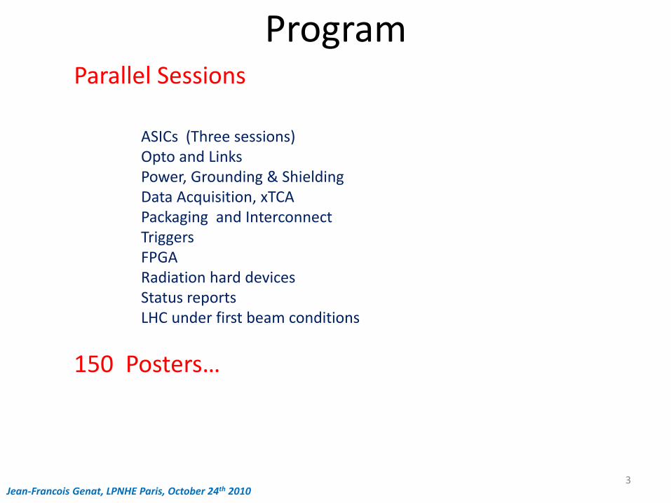
Program Parallel Sessions
ASICs (Three sessions) Opto and Links Power, Grounding & Shielding Data Acquisition, xTCA Packaging and Interconnect Triggers FPGA Radiation hard devices Status reports LHC under first beam conditions
150 Posters…
Jean-Francois Genat, LPNHE Paris, October 24th 2010 3
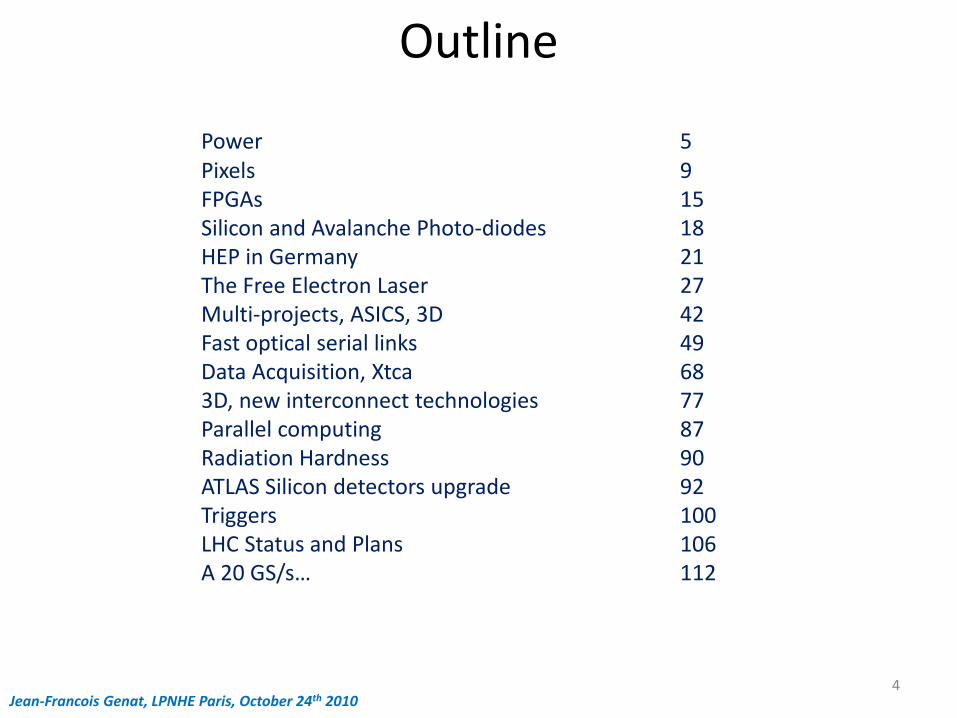
Outline Power 5 Pixels 9 FPGAs 15 Silicon and Avalanche Photo-diodes 18 HEP in Germany 21 The Free Electron Laser 27 Multi-projects, ASICS, 3D 42 Fast optical serial links 49 Data Acquisition, Xtca 68 3D, new interconnect technologies 77 Parallel computing 87 Radiation Hardness 90 ATLAS Silicon detectors upgrade 92 Triggers 100 LHC Status and Plans 106 A 20 GS/s… 112
Jean-Francois Genat, LPNHE Paris, October 24th 2010 4
Power DC-DC Converters vs Serial
Jean-Francois Genat, LPNHE Paris, October 24th 2010 5
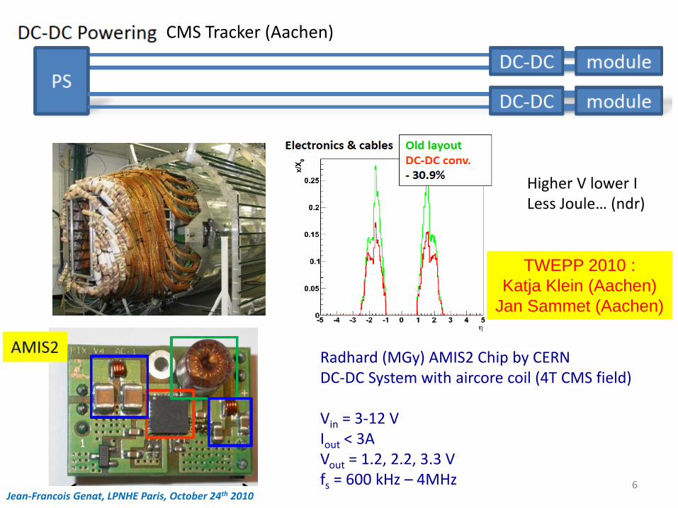
Radhard (MGy) AMIS2 Chip by CERN DC-DC System with aircore coil (4T CMS field) Vin = 3-12 V Iout < 3A Vout = 1.2, 2.2, 3.3 V fs = 600 kHz – 4MHz
TWEPP 2010 :
Katja Klein (Aachen)
Jan Sammet (Aachen)
CMS Tracker (Aachen)
Jean-Francois Genat, LPNHE Paris, October 24th 2010 6
Higher V lower I Less Joule… (ndr)
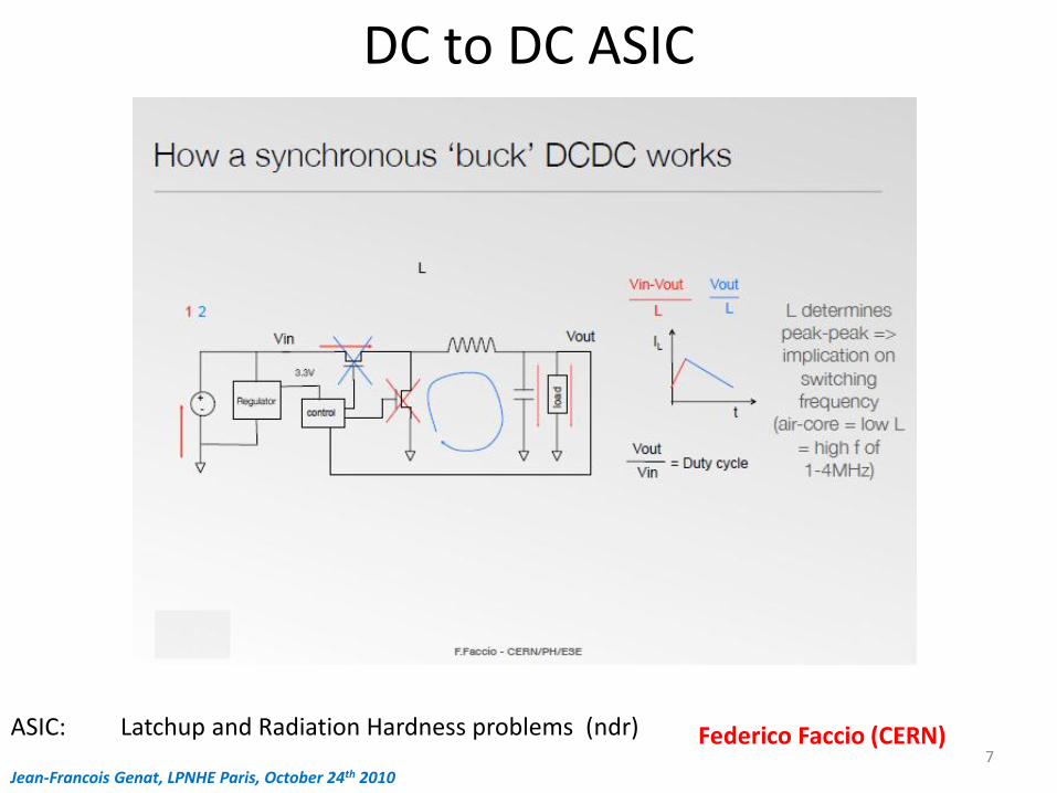
DC to DC ASIC
Jean-Francois Genat, LPNHE Paris, October 24th 2010 7
Federico Faccio (CERN) ASIC: Latchup and Radiation Hardness problems (ndr)
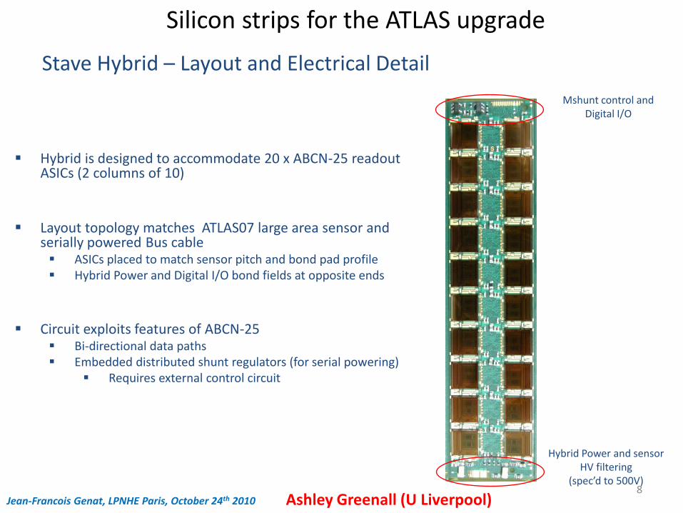
Stave Hybrid – Layout and Electrical Detail
Hybrid is designed to accommodate 20 x ABCN-25 readout ASICs (2 columns of 10)
Layout topology matches ATLAS07 large area sensor and serially powered Bus cable ASICs placed to match sensor pitch and bond pad profile Hybrid Power and Digital I/O bond fields at opposite ends
Circuit exploits features of ABCN-25 Bi-directional data paths Embedded distributed shunt regulators (for serial powering)
Requires external control circuit
Mshunt control and Digital I/O
Hybrid Power and sensor HV filtering
(spec’d to 500V)
Silicon strips for the ATLAS upgrade
Jean-Francois Genat, LPNHE Paris, October 24th 2010 Ashley Greenall (U Liverpool) 8
Pixels
Jean-Francois Genat, LPNHE Paris, October 24th 2010 9
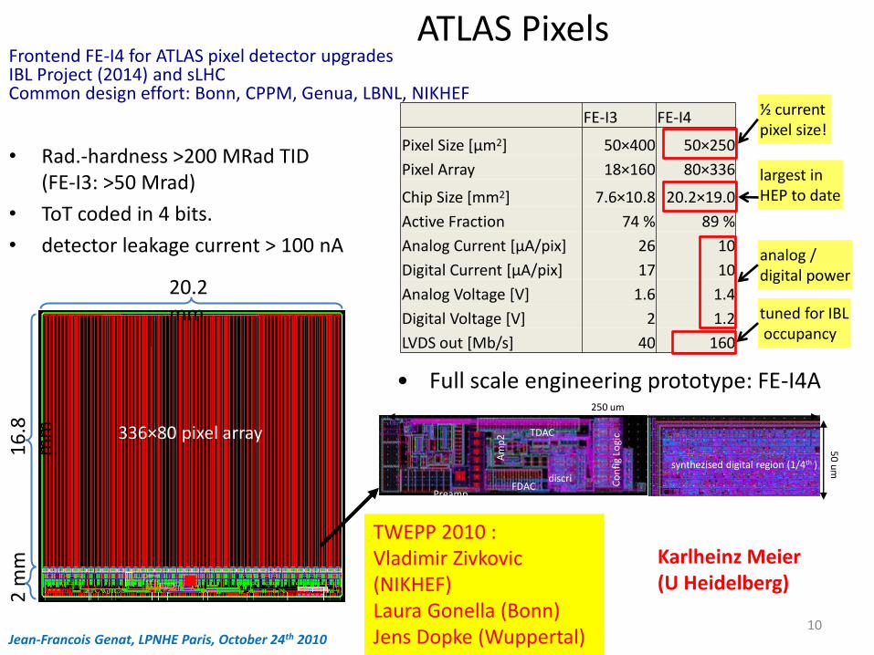
• Rad.-hardness >200 MRad TID (FE-I3: >50 Mrad)
• ToT coded in 4 bits.
• detector leakage current > 100 nA
FE-I3 FE-I4
Pixel Size [μm2] 50×400 50×250
Pixel Array 18×160 80×336
Chip Size [mm2] 7.6×10.8 20.2×19.0
Active Fraction 74 % 89 %
Analog Current [μA/pix] 26 10
Digital Current [μA/pix] 17 10
Analog Voltage [V] 1.6 1.4
Digital Voltage [V] 2 1.2
LVDS out [Mb/s] 40 160
largest in HEP to date
analog / digital power
tuned for IBL occupancy
½ current pixel size!
336×80 pixel array
16
.8
mm
2
mm
20.2 mm
• Full scale engineering prototype: FE-I4A
Preamp A
mp
2
FDAC
TDAC
Co
nfi
g Lo
gic
discri
50
um
250 um
synthezised digital region (1/4th )
Frontend FE-I4 for ATLAS pixel detector upgrades IBL Project (2014) and sLHC Common design effort: Bonn, CPPM, Genua, LBNL, NIKHEF
TWEPP 2010 : Vladimir Zivkovic (NIKHEF) Laura Gonella (Bonn) Jens Dopke (Wuppertal)
Karlheinz Meier (U Heidelberg)
Jean-Francois Genat, LPNHE Paris, October 24th 2010
ATLAS Pixels
10
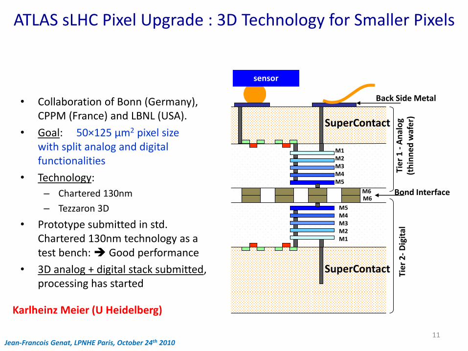
ATLAS sLHC Pixel Upgrade : 3D Technology for Smaller Pixels
• Collaboration of Bonn (Germany), CPPM (France) and LBNL (USA).
• Goal: 50×125 μm2 pixel size with split analog and digital functionalities
• Technology:
– Chartered 130nm
– Tezzaron 3D
• Prototype submitted in std. Chartered 130nm technology as a test bench: Good performance
• 3D analog + digital stack submitted, processing has started
M5 M4 M3 M2 M1
M6
SuperContact
M1 M2 M3 M4 M5
M6
SuperContact
Bond Interface
Tie
r 2
- D
igit
al
Tie
r 1
- A
nal
og
(th
inn
ed
waf
er)
Back Side Metal
sensor
Karlheinz Meier (U Heidelberg)
Jean-Francois Genat, LPNHE Paris, October 24th 2010 11
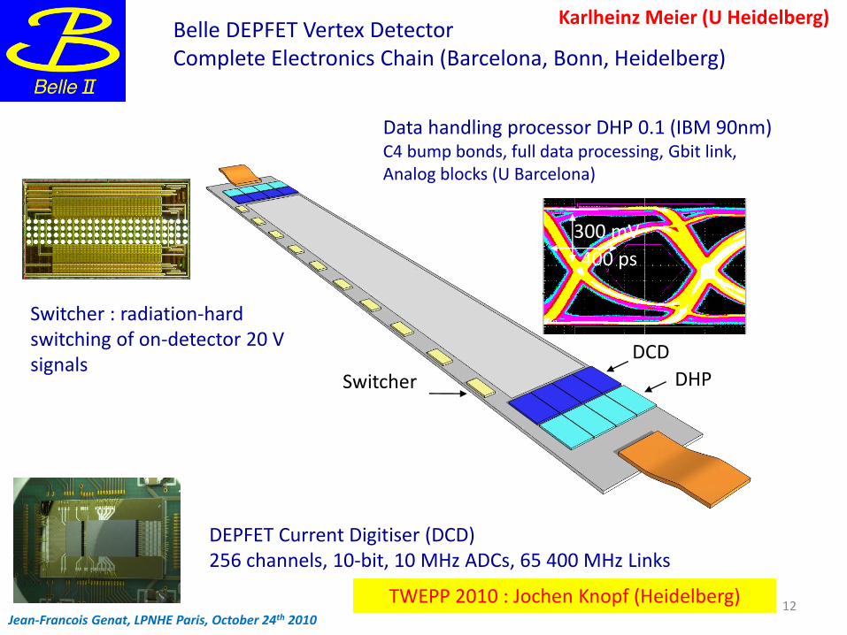
Belle DEPFET Vertex Detector Complete Electronics Chain (Barcelona, Bonn, Heidelberg)
Switcher : radiation-hard switching of on-detector 20 V signals
DEPFET Current Digitiser (DCD) 256 channels, 10-bit, 10 MHz ADCs, 65 400 MHz Links
DHP
DCD
Switcher
300 mV
400 ps
Data handling processor DHP 0.1 (IBM 90nm) C4 bump bonds, full data processing, Gbit link, Analog blocks (U Barcelona)
TWEPP 2010 : Jochen Knopf (Heidelberg)
Karlheinz Meier (U Heidelberg)
Jean-Francois Genat, LPNHE Paris, October 24th 2010 12
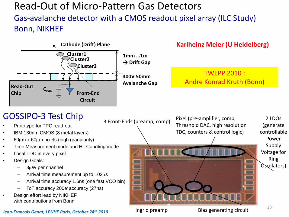
Read-Out of Micro-Pattern Gas Detectors Gas-avalanche detector with a CMOS readout pixel array (ILC Study) Bonn, NIKHEF
Cluster3
Cathode (Drift) Plane
Cluster2 Cluster1
Read-Out Chip
1mm …1m → Drift Gap
400V 50mm Avalanche Gap
Front-End Circuit
CPAR
2 LDOs (generate
controllable Power Supply
Voltage for Ring
Oscillators)
Pixel (pre-amplifier, comp, Threshold DAC, high resolution TDC, counters & control logic)
3 Front-Ends (preamp, comp)
Ingrid preamp Bias generating circuit
GOSSIPO-3 Test Chip • Prototype for TPC read-out
• IBM 130nm CMOS (8 metal layers)
• 60mm x 60mm pixels (high granularity)
• Time Measurement mode and Hit Counting mode
• Local TDC in every pixel
• Design Goals:
– 3mW per channel
– Arrival time measurement up to 102ms
– Arrival time accuracy 1.6ns (one fast VCO bin)
– ToT accuracy 200e- accuracy (27ns)
• Design effort lead by NIKHEF
with contributions from Bonn
TWEPP 2010 : Andre Konrad Kruth (Bonn)
Karlheinz Meier (U Heidelberg)
Jean-Francois Genat, LPNHE Paris, October 24th 2010 13
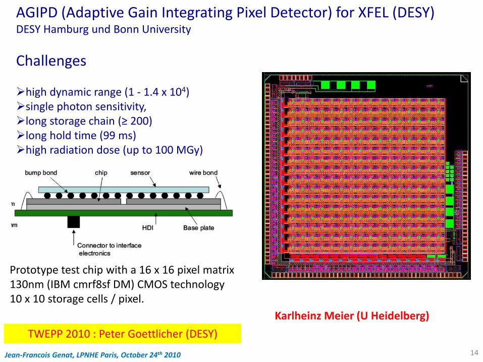
AGIPD (Adaptive Gain Integrating Pixel Detector) for XFEL (DESY) DESY Hamburg und Bonn University
Challenges high dynamic range (1 - 1.4 x 10⁴) single photon sensitivity, long storage chain (≥ 200) long hold time (99 ms) high radiation dose (up to 100 MGy)
Prototype test chip with a 16 x 16 pixel matrix 130nm (IBM cmrf8sf DM) CMOS technology 10 x 10 storage cells / pixel.
TWEPP 2010 : Peter Goettlicher (DESY)
Karlheinz Meier (U Heidelberg)
Jean-Francois Genat, LPNHE Paris, October 24th 2010 14
FPGAs
Jean-Francois Genat, LPNHE Paris, October 24th 2010 15
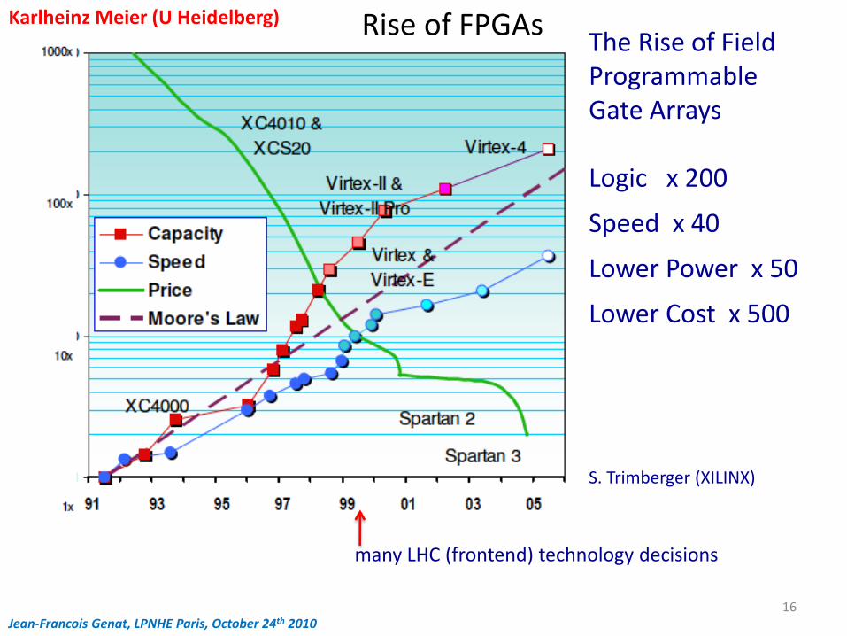
The Rise of Field Programmable Gate Arrays Logic x 200
Speed x 40
Lower Power x 50
Lower Cost x 500 S. Trimberger (XILINX)
many LHC (frontend) technology decisions
Karlheinz Meier (U Heidelberg) Rise of FPGAs
Jean-Francois Genat, LPNHE Paris, October 24th 2010 16
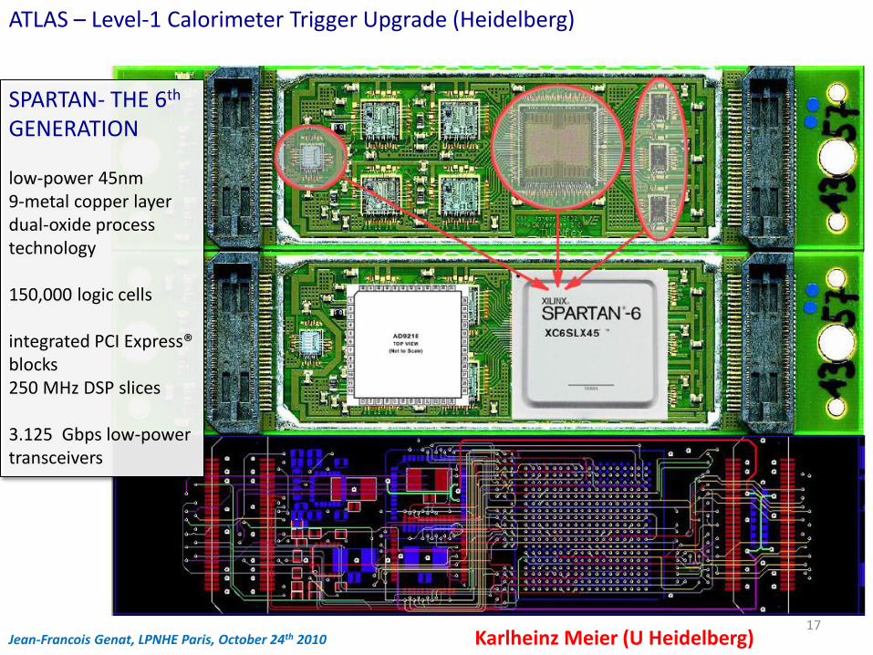
SPARTAN- THE 6th GENERATION low-power 45nm 9-metal copper layer dual-oxide process technology 150,000 logic cells integrated PCI Express® blocks 250 MHz DSP slices 3.125 Gbps low-power transceivers
ATLAS – Level-1 Calorimeter Trigger Upgrade (Heidelberg)
Karlheinz Meier (U Heidelberg) Jean-Francois Genat, LPNHE Paris, October 24th 2010 17
Silicon Photo-Multipliers Avalanche Photo-diodes
Jean-Francois Genat, LPNHE Paris, October 24th 2010 18
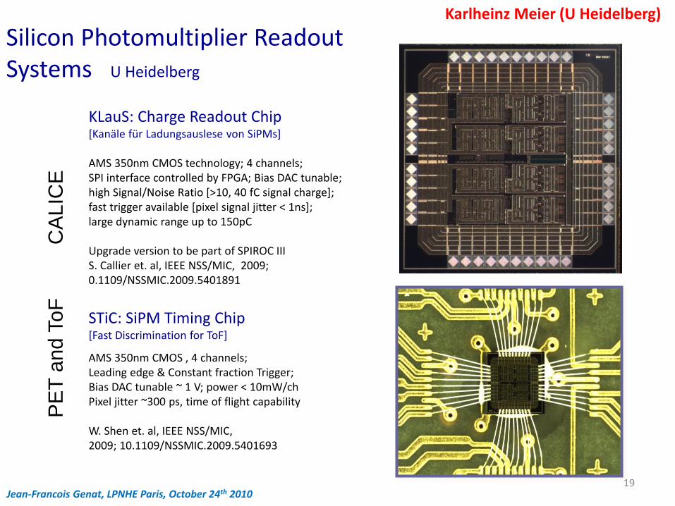
Silicon Photomultiplier Readout Systems U Heidelberg
KLauS: Charge Readout Chip [Kanäle für Ladungsauslese von SiPMs] AMS 350nm CMOS technology; 4 channels; SPI interface controlled by FPGA; Bias DAC tunable; high Signal/Noise Ratio [>10, 40 fC signal charge]; fast trigger available [pixel signal jitter < 1ns]; large dynamic range up to 150pC Upgrade version to be part of SPIROC III S. Callier et. al, IEEE NSS/MIC, 2009; 0.1109/NSSMIC.2009.5401891
STiC: SiPM Timing Chip [Fast Discrimination for ToF]
AMS 350nm CMOS , 4 channels; Leading edge & Constant fraction Trigger; Bias DAC tunable ~ 1 V; power < 10mW/ch Pixel jitter ~300 ps, time of flight capability W. Shen et. al, IEEE NSS/MIC, 2009; 10.1109/NSSMIC.2009.5401693
CA
LIC
E
PE
T a
nd T
oF
Karlheinz Meier (U Heidelberg)
Jean-Francois Genat, LPNHE Paris, October 24th 2010 19
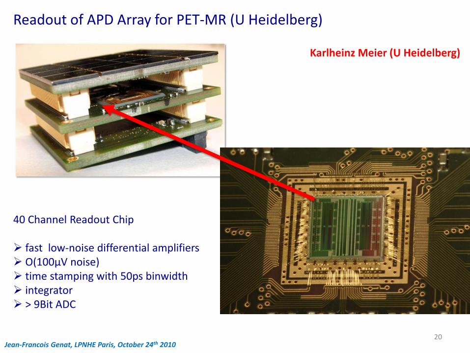
Readout of APD Array for PET-MR (U Heidelberg)
40 Channel Readout Chip fast low-noise differential amplifiers O(100µV noise) time stamping with 50ps binwidth integrator > 9Bit ADC
Karlheinz Meier (U Heidelberg)
Jean-Francois Genat, LPNHE Paris, October 24th 2010 20
HEP in Germany
Jean-Francois Genat, LPNHE Paris, October 24th 2010 21
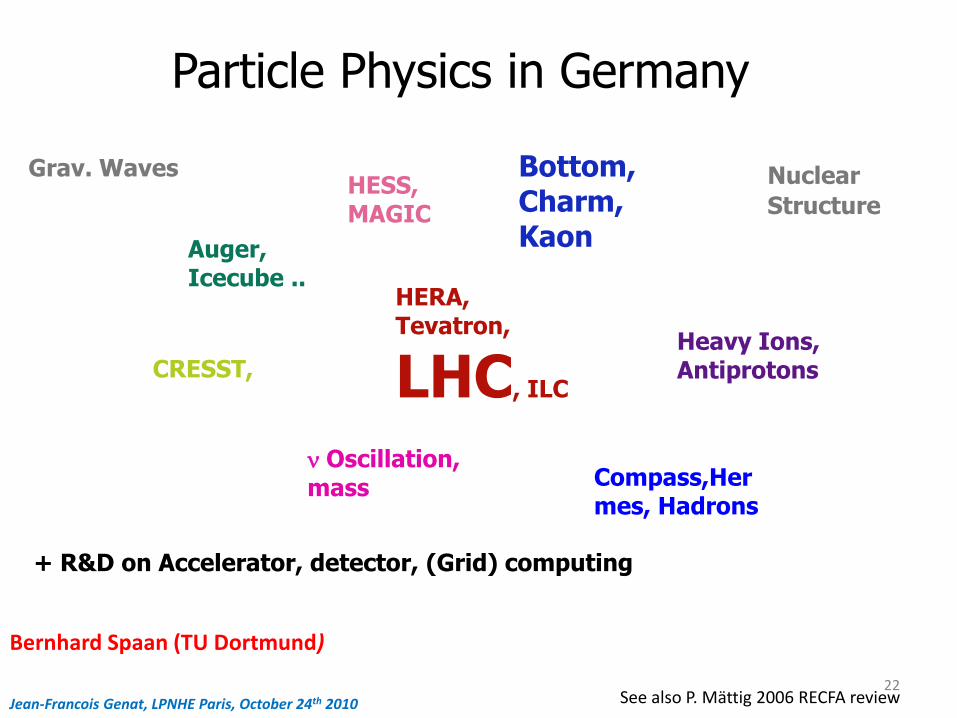
HERA, Tevatron,
LHC, ILC
Compass,Hermes, Hadrons
Oscillation, mass
Auger, Icecube ..
Heavy Ions, Antiprotons
Bottom, Charm, Kaon
CRESST,
HESS, MAGIC
Grav. Waves Nuclear
Structure
Particle Physics in Germany
+ R&D on Accelerator, detector, (Grid) computing
Bernhard Spaan (TU Dortmund)
See also P. Mättig 2006 RECFA review Jean-Francois Genat, LPNHE Paris, October 24th 2010 22
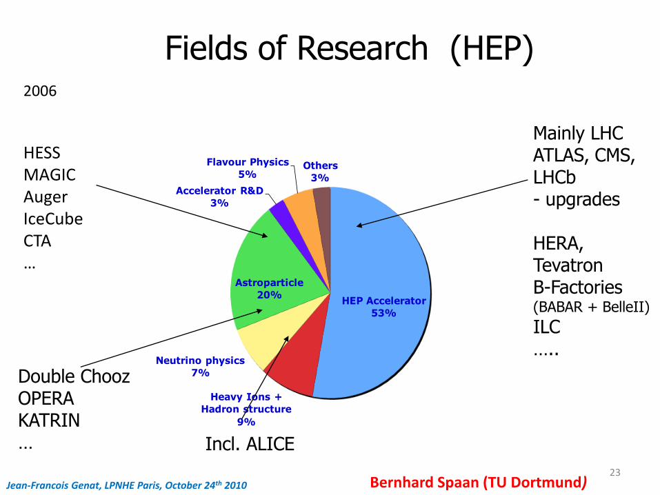
Fields of Research (HEP)
HEP Accelerator
53%
Heavy Ions +
Hadron structure
9%
Neutrino physics
7%
Astroparticle
20%
Accelerator R&D
3%
Flavour Physics
5%Others
3%
2006
Mainly LHC ATLAS, CMS, LHCb - upgrades HERA, Tevatron B-Factories (BABAR + BelleII)
ILC …..
Incl. ALICE
Double Chooz OPERA KATRIN …
HESS MAGIC Auger IceCube CTA …
Bernhard Spaan (TU Dortmund) Jean-Francois Genat, LPNHE Paris, October 24th 2010 23
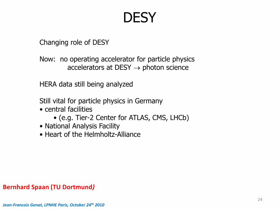
DESY
Changing role of DESY Now: no operating accelerator for particle physics accelerators at DESY photon science HERA data still being analyzed Still vital for particle physics in Germany • central facilities
• (e.g. Tier-2 Center for ATLAS, CMS, LHCb) • National Analysis Facility • Heart of the Helmholtz-Alliance
Bernhard Spaan (TU Dortmund)
Jean-Francois Genat, LPNHE Paris, October 24th 2010 24
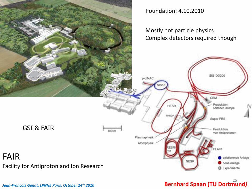
FAIR Facility for Antiproton and Ion Research
Foundation: 4.10.2010
GSI & FAIR
Mostly not particle physics Complex detectors required though
Bernhard Spaan (TU Dortmund) Jean-Francois Genat, LPNHE Paris, October 24th 2010 25
Conclusions
Strong research in particle physics Strong focus on LHC programme (incl. Upgrade) DESY changed profile – still vital for particle physics Free Electron Laser development (ndr) Somewhat complicated structure/funding regime Participation in all areas –
• Detector R&D and construction • Electronics • Data Analysis • Computing • Accelerator Physics
Future strategy in preparation
Bernhard Spaan (TU Dortmund)
Jean-Francois Genat, LPNHE Paris, October 24th 2010 26
The Free Electron Laser (FEL)
Jean-Francois Genat, LPNHE Paris, October 24th 2010 27
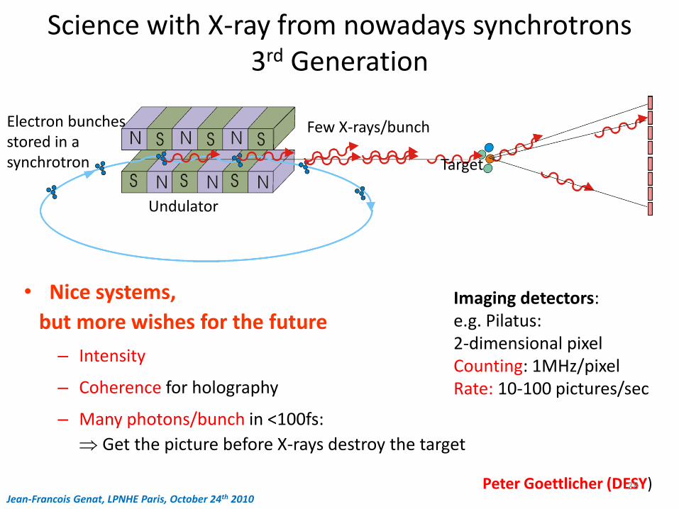
Science with X-ray from nowadays synchrotrons 3rd Generation
• Nice systems,
but more wishes for the future
– Intensity
– Coherence for holography
– Many photons/bunch in <100fs:
Get the picture before X-rays destroy the target
Undulator
Electron bunches stored in a synchrotron
Few X-rays/bunch
Target
Imaging detectors: e.g. Pilatus: 2-dimensional pixel Counting: 1MHz/pixel Rate: 10-100 pictures/sec
Peter Goettlicher (DESY) Jean-Francois Genat, LPNHE Paris, October 24th 2010
28
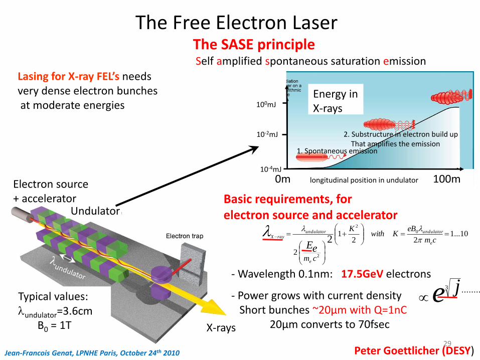
- Wavelength 0.1nm: 17.5GeV electrons
- Power grows with current density Short bunches ~20µm with Q=1nC 20µm converts to 70fsec
The Free Electron Laser
Lasing for X-ray FEL’s needs very dense electron bunches at moderate energies
X-ray power/burst
10...122
1
2
0
2
2
2
cm
eBKwith
K
cm
e
undulator
e
undulatorrayX
eE
The SASE principle Self amplified spontaneous saturation emission
0m longitudinal position in undulator 100m
1. Spontaneous emission
2. Substructure in electron build up That amplifies the emission
10-4mJ
10-2mJ
100mJ
........3 je
Undulator Basic requirements, for electron source and accelerator
Energy in X-rays
Electron source + accelerator
X-rays
Typical values: undulator=3.6cm B0 = 1T
Jean-Francois Genat, LPNHE Paris, October 24th 2010 Peter Goettlicher (DESY) 29
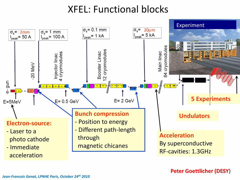
XFEL: Functional blocks
Electron-source: - Laser to a photo cathode - Immediate acceleration
Bunch compression - Position to energy - Different path-length through magnetic chicanes
Acceleration By superconductive RF-cavities: 1.3GHz
Undulators
2mm 20mm
5 Experiments
Experiment
Peter Goettlicher (DESY) Jean-Francois Genat, LPNHE Paris, October 24th 2010
30
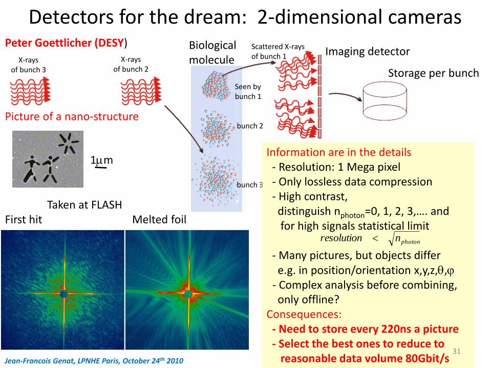
Detectors for the dream: 2-dimensional cameras Scattered X-rays of bunch 1 X-rays
of bunch 2 X-rays of bunch 3
Biological molecule
Seen by bunch 1 bunch 2 bunch 3
Imaging detector
Storage per bunch
Picture of a nano-structure Taken at FLASH First hit Melted foil
Information are in the details - Resolution: 1 Mega pixel - Only lossless data compression - High contrast, distinguish nphoton=0, 1, 2, 3,…. and for high signals statistical limit - Many pictures, but objects differ e.g. in position/orientation x,y,z,q,j - Complex analysis before combining, only offline? Consequences: - Need to store every 220ns a picture - Select the best ones to reduce to reasonable data volume 80Gbit/s
photonnresolution
1mm
Peter Goettlicher (DESY)
Jean-Francois Genat, LPNHE Paris, October 24th 2010 31
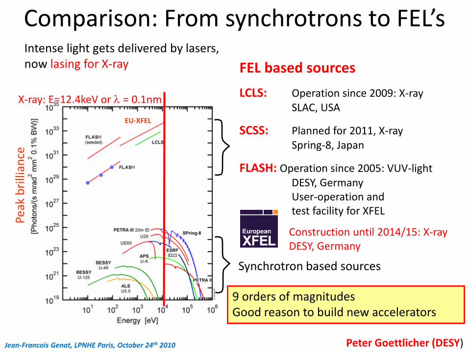
Comparison: From synchrotrons to FEL’s Intense light gets delivered by lasers, now lasing for X-ray
Synchrotron based sources
FEL based sources
LCLS: Operation since 2009: X-ray SLAC, USA
SCSS: Planned for 2011, X-ray Spring-8, Japan
FLASH: Operation since 2005: VUV-light DESY, Germany User-operation and test facility for XFEL
Construction until 2014/15: X-ray DESY, Germany
X-ray: E=12.4keV or = 0.1nm
9 orders of magnitudes Good reason to build new accelerators
EU-XFEL
Peak
bri
llian
ce
Peter Goettlicher (DESY) Jean-Francois Genat, LPNHE Paris, October 24th 2010
The European XFEL:
Acceleration tunnel
Undulators, 5 X-ray tunnels upgrade to 10 tunnels
Experimental hall
source
Injector hall Access shaft
FLASH
PETRA3
DESY
HERA
Hamburg city centre 7 km
Peter Goettlicher (DESY) Jean-Francois Genat, LPNHE Paris, October 24th 2010
General detector concepts: Electrical and Connectivity
Bump bond/pixel
Wire bonds to a High-Density board
Environment Scattering quality
Copper cables Clocks, TCP/IP-100MbE
Fibre optics UDP-10GbE Camera head
Crates in racks IT-center
Sync. clocks Bunch quality
- Three consortia for cameras - Each covering multipurpose science, each not all, all differently specialized Common development
for all at XFEL-experiments
Experiment
Peter Goettlicher (DESY) Jean-Francois Genat, LPNHE Paris, October 24th 2010 34
2-dimension cameras
Different physics by different technical approaches
Adaptive Gain Integrated Pixel Detector Institutes: Bonn(University), DESY, Hamburg(University), PSI(Villingen) Reference: B. Henrich, et al., Nucl. Instr. and Meth. A (2010), doi:10.1016/j.nima.2010.06.107
DEPMOS Sensor with Signal Compression Institutes: MPI-HLL Munich, DESY, Heidelberg(Univ.), Poly. Milano, Bergamo(Univ.), Siegen(Univ) Reference: M. Porro, et al., Nucl. Instr. and Meth. A (2010), doi:10.1016/j.nima.2010.02.254
Large Pixel Detector Institutes: STFC/RAL, Glasgow(University) Reference: S.R.Burge et al., Large Pixel Detector for the European X-ray Free Electron Laser,
11th European Symposium on Semiconductor Detectors, June 2009 conference proceedings.
DSSC
LPD
AGIPD DSSC LPD
Pixel 200 x 200mm2 236mm hexagons
with a DEPFET
500 x 500mm2
Approach for
dynamic range
Automatic gain
switching
Compression by
DEPFET in pixel
3 parallel gains
Storage per
bunch
Analogue with
analog ASIC-out.
Digital,
1ADC/pixel
Analogue with
digital ASIC-out.
Common items: Sensor-studies, ASIC in 130nm-technology, DAQ-systems
AGIPD
Peter Goettlicher (DESY) Jean-Francois Genat, LPNHE Paris, October 24th 2010 35
Camera Analog ASIC
0 5000 15000 10000 0
0.5
1.5
1.0
Ou
tpu
t vo
ltag
e [V
]
No
ise
[1
2ke
V p
ho
ton
eq
uiv
alen
t]
0
50
100
150
Feedback capacitors
Noise of preamplifier
Bo
nd
pad
to
pix
el
Automatic gain switching: - Gain switches, when output exceeds threshold - Adding instead of replacing capacitors avoids charge losses
Analogue storage of amplitude and gain - reduces output lines
Multiplexing: Just one differential output For 32 x 32 pixels
Optimized capacitors to store maximum number of picture of a train not all 2700 will be possible realistic: ~ 200
Random address overwriting allows handling of an external decision of best scatterings
Constraint Everything has to fit behind the pixel 200µm x 200µm
Peter Goettlicher (DESY)
AGIPD
Jean-Francois Genat, LPNHE Paris, October 24th 2010 36
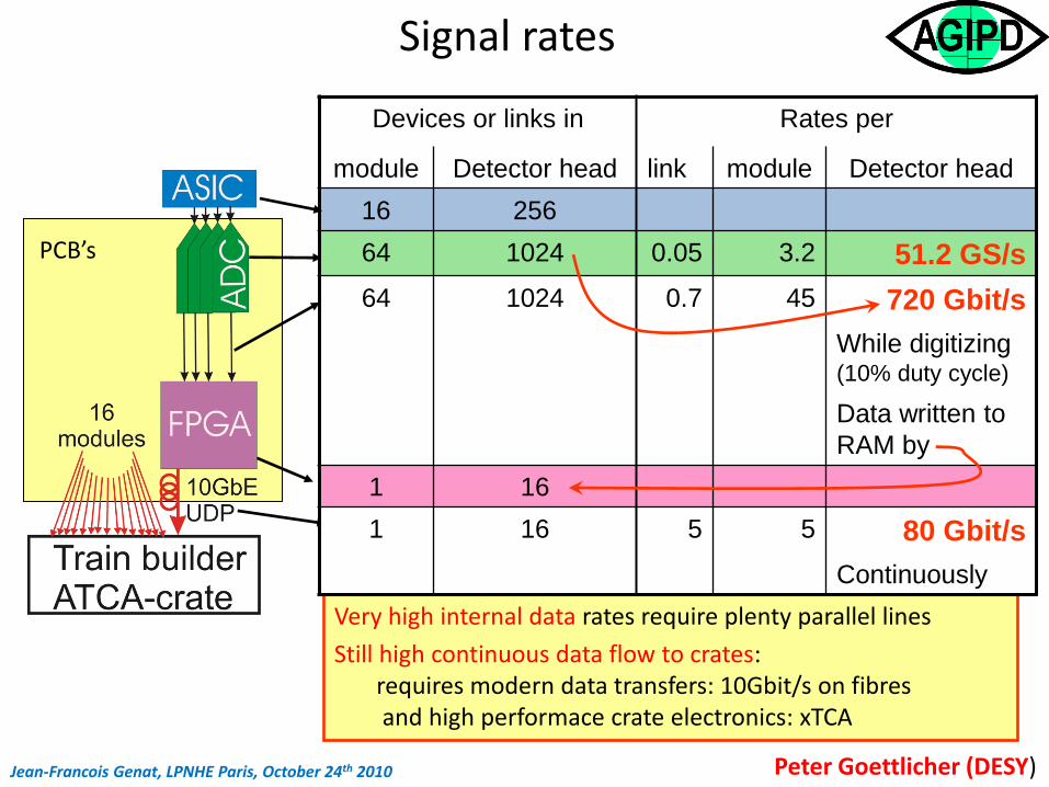
Signal rates
Very high internal data rates require plenty parallel lines
Still high continuous data flow to crates: requires modern data transfers: 10Gbit/s on fibres and high performace crate electronics: xTCA
Devices or links in Rates per
module Detector head link module Detector head
16 256
64 1024 0.05 3.2 51.2 GS/s
64 1024 0.7 45 720 Gbit/s
While digitizing (10% duty cycle)
Data written to
RAM by
1 16
1 16 5 5 80 Gbit/s
Continuously
PCB’s
Peter Goettlicher (DESY) Jean-Francois Genat, LPNHE Paris, October 24th 2010
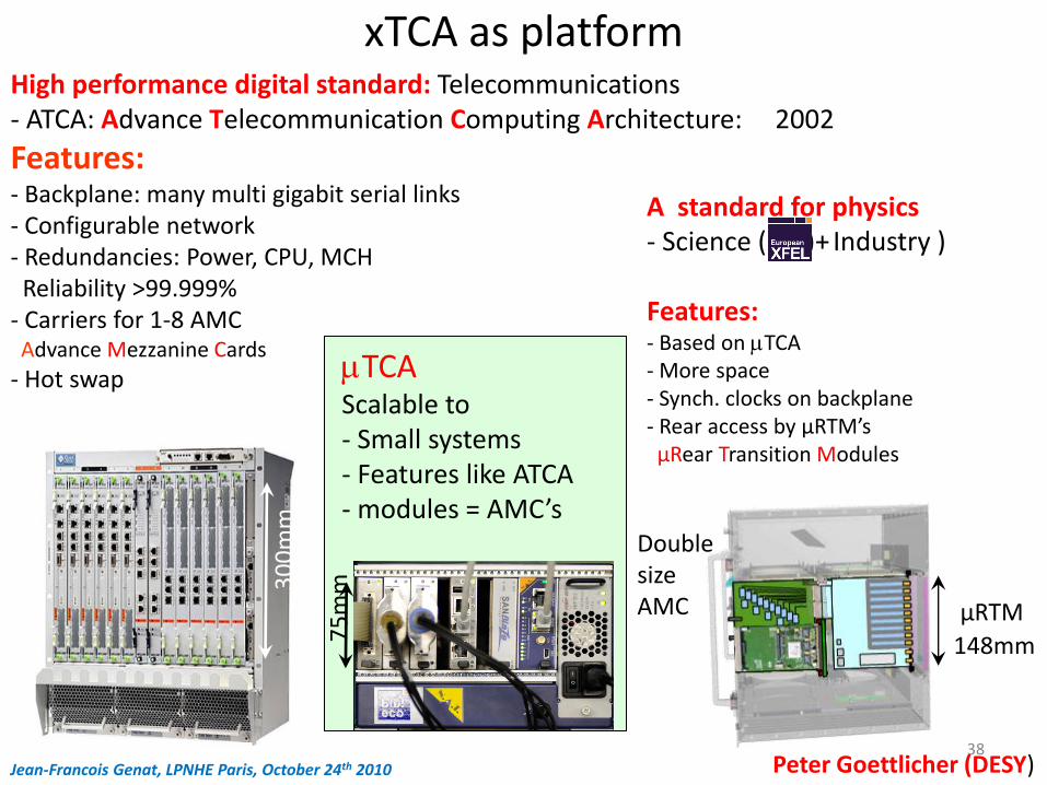
mTCA Scalable to - Small systems - Features like ATCA - modules = AMC’s
xTCA as platform High performance digital standard: Telecommunications - ATCA: Advance Telecommunication Computing Architecture: 2002
Features: - Backplane: many multi gigabit serial links - Configurable network - Redundancies: Power, CPU, MCH Reliability >99.999% - Carriers for 1-8 AMC Advance Mezzanine Cards
- Hot swap
A standard for physics- Science ( )+ Industry )
Features: - Based on mTCA - More space - Synch. clocks on backplane - Rear access by µRTM’s µRear Transition Modules
30
0m
m
75
mm
µRTM
148mm
Double size AMC
Peter Goettlicher (DESY) Jean-Francois Genat, LPNHE Paris, October 24th 2010 38
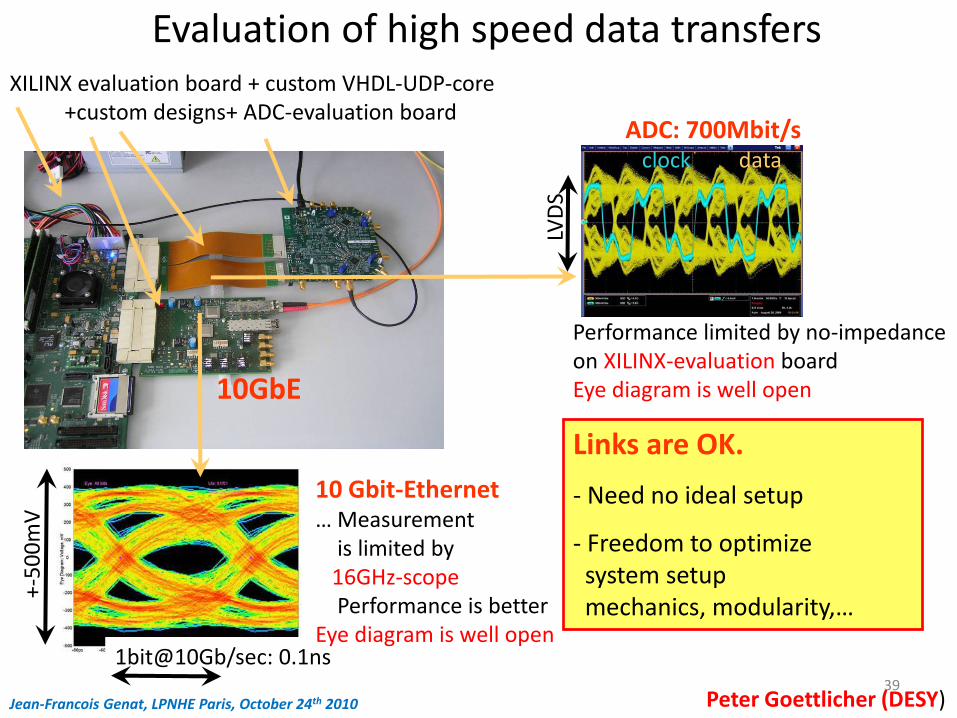
Evaluation of high speed data transfers XILINX evaluation board + custom VHDL-UDP-core +custom designs+ ADC-evaluation board
1bit@10Gb/sec: 0.1ns
10 Gbit-Ethernet … Measurement is limited by 16GHz-scope Performance is better Eye diagram is well open
+-5
00
mV
LVD
S
ADC: 700Mbit/s clock and data
Performance limited by no-impedance on XILINX-evaluation board Eye diagram is well open 10GbE
Links are OK.
- Need no ideal setup
- Freedom to optimize system setup mechanics, modularity,…
Peter Goettlicher (DESY) Jean-Francois Genat, LPNHE Paris, October 24th 2010 39
XFEL status
• European XFEL will deliver the highest peak brilliance and bunch rate.
• Need of excellent accelerator performance: Size and energy of bunch.
• Dedicated regulations in modern technologies needed.
Developments and tests at FLASH are on going with good results.
• That leads to the use of modern standards in science: ATCA, mTCA.
Adapting them to the needs (PICMG) and first modules are available.
• Demanding dedicated detectors (Pixel cameras) are being developed.
Ongoing developments for full chain with high signal and data throughput: – Sensors, ASIC’s, detector heads and DAQ systems
– e.g. 4.5MHz picture rate, 80 Gbit/s out of small detector heads
• All the effort opens new fields of science:
Capturing a scattering picture with one flash of X-rays.
• Thanks to all the work packages and consortia for providing material
• More information on www.xfel.eu
http://hasylab.desy.de/instrumentation/detectors/index_eng.html
Peter Goettlicher (DESY) Jean-Francois Genat, LPNHE Paris, October 24th 2010 40
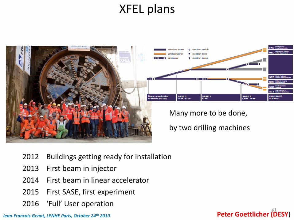
XFEL plans
• September 3rd 2010: First photon tunnel drilling finished
2012 Buildings getting ready for installation
2013 First beam in injector
2014 First beam in linear accelerator
2015 First SASE, first experiment
2016 ‘Full’ User operation
Many more to be done,
by two drilling machines
Peter Goettlicher (DESY) Jean-Francois Genat, LPNHE Paris, October 24th 2010 41
Multi-projects, ASICS, 3D
Jean-Francois Genat, LPNHE Paris, October 24th 2010 42
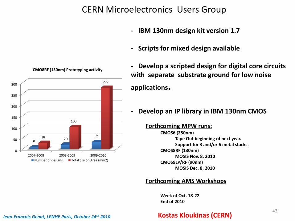
CERN Microelectronics Users Group
0
50
100
150
200
250
300
2007-2008 2008-2009 2009-2010
8 20
32 28
100
277
CMO8RF (130nm) Prototyping activity
Number of designs Total Silicon Area (mm2)
- IBM 130nm design kit version 1.7 - Scripts for mixed design available
- Develop a scripted design for digital core circuits with separate substrate ground for low noise
applications.
- Develop an IP library in IBM 130nm CMOS
Forthcoming MPW runs: CMOS6 (250nm)
Tape Out beginning of next year. Support for 3 and/or 6 metal stacks.
CMOS8RF (130nm) MOSIS Nov. 8, 2010
CMOS9LP/RF (90nm) MOSIS Dec. 8, 2010
Forthcoming AMS Workshops
Week of Oct. 18-22 End of 2010
Jean-Francois Genat, LPNHE Paris, October 24th 2010 Kostas Kloukinas (CERN) 43
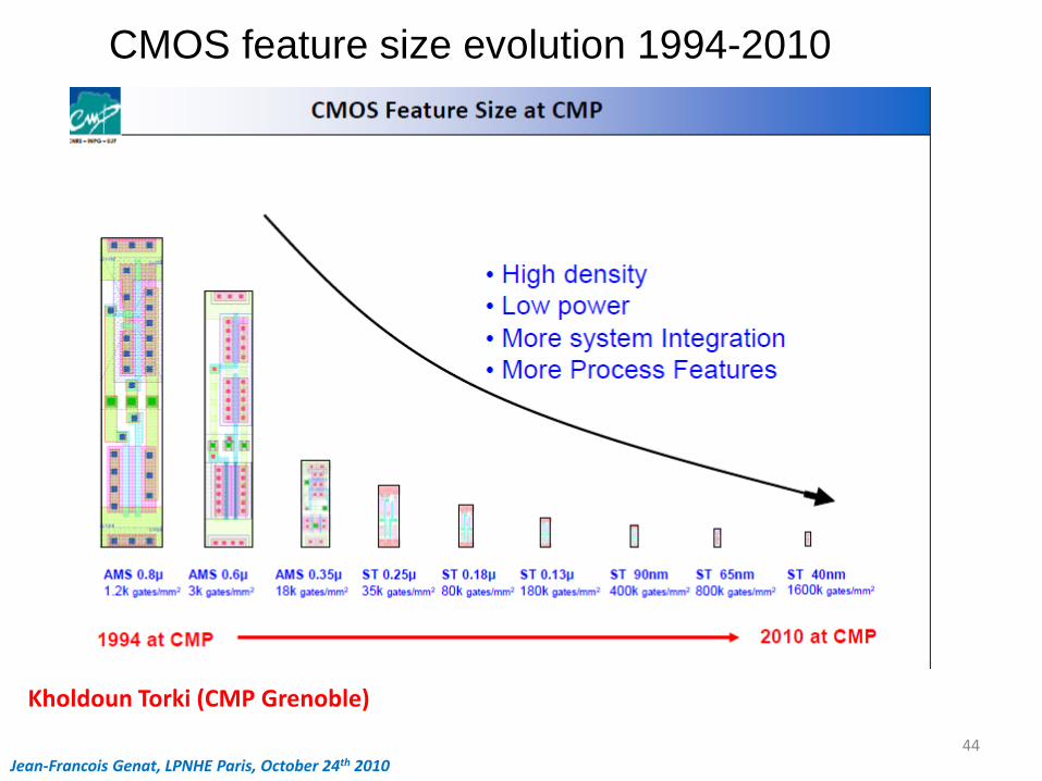
CMOS feature size evolution 1994-2010
Kholdoun Torki (CMP Grenoble)
Jean-Francois Genat, LPNHE Paris, October 24th 2010 44
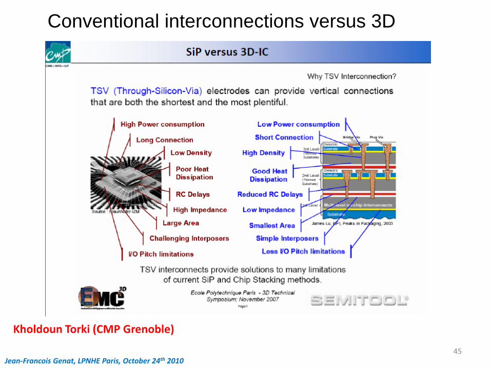
Conventional interconnections versus 3D
Kholdoun Torki (CMP Grenoble)
Jean-Francois Genat, LPNHE Paris, October 24th 2010 45
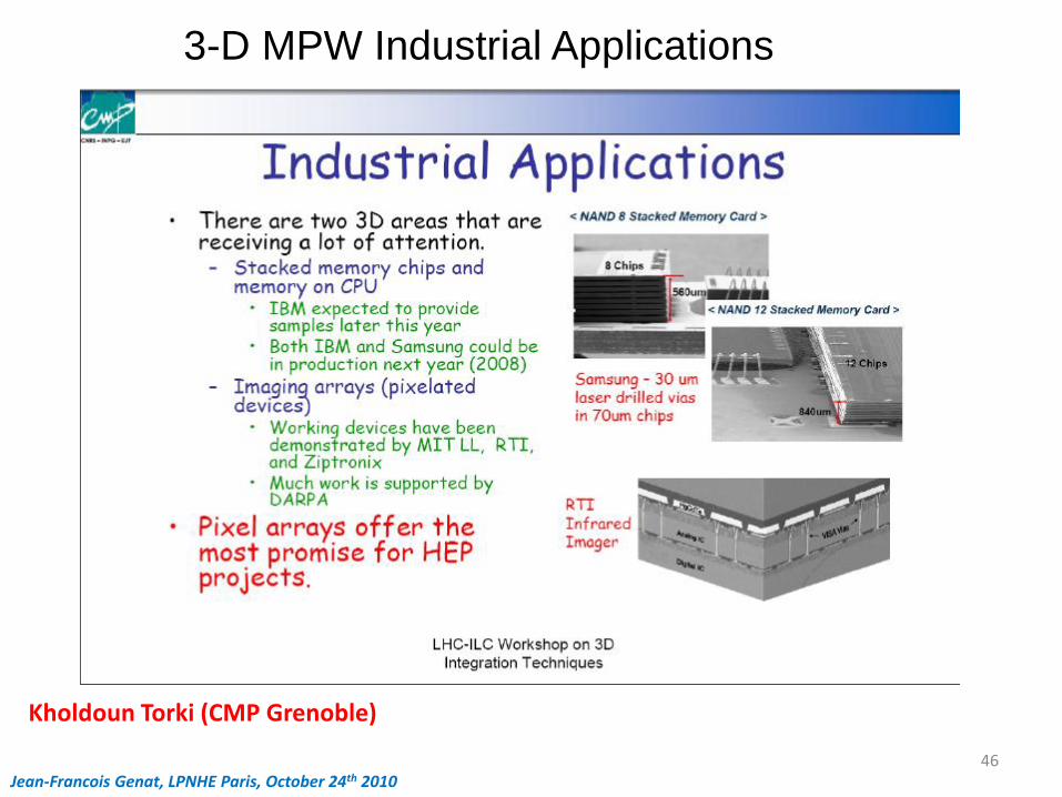
3-D MPW Industrial Applications
Kholdoun Torki (CMP Grenoble)
Jean-Francois Genat, LPNHE Paris, October 24th 2010 46
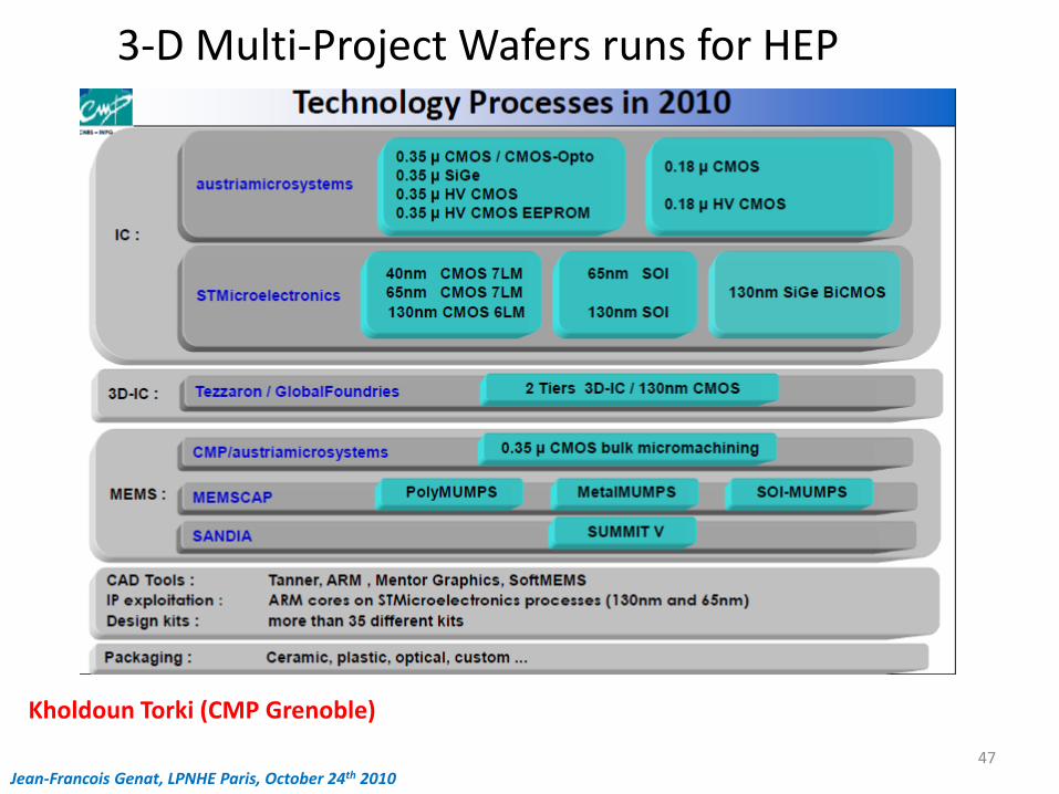
3-D Multi-Project Wafers runs for HEP
Kholdoun Torki (CMP Grenoble)
Jean-Francois Genat, LPNHE Paris, October 24th 2010 47
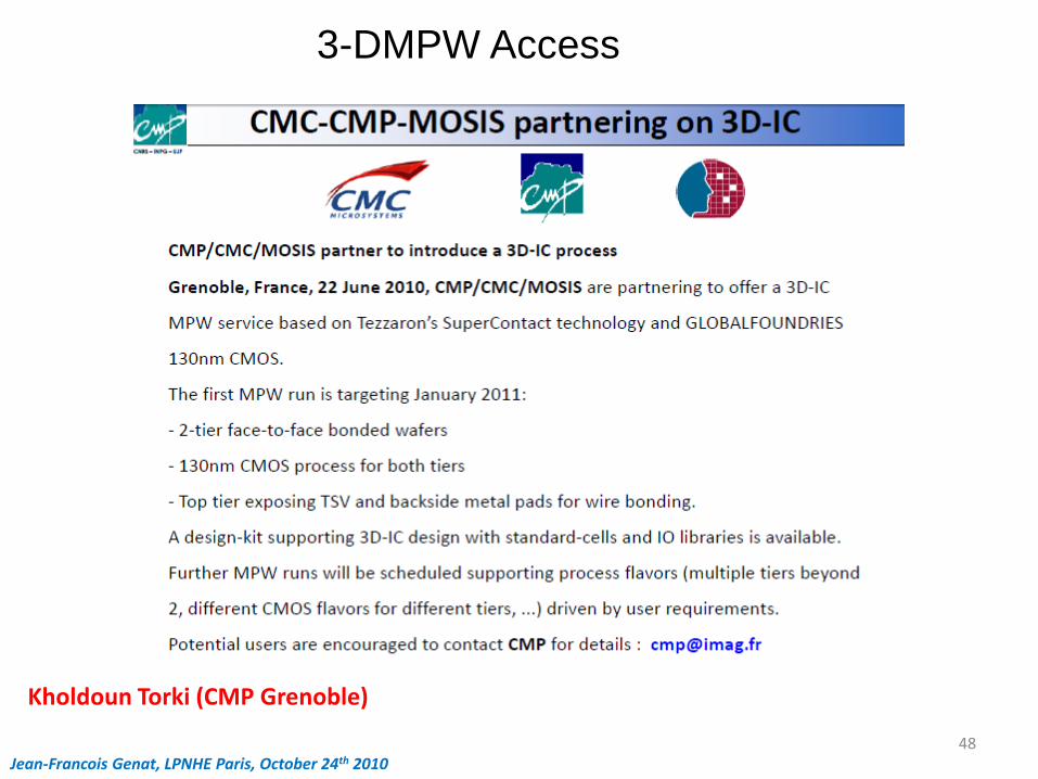
3-DMPW Access
Kholdoun Torki (CMP Grenoble)
Jean-Francois Genat, LPNHE Paris, October 24th 2010 48
Fast optical serial links
Jean-Francois Genat, LPNHE Paris, October 24th 2010 49
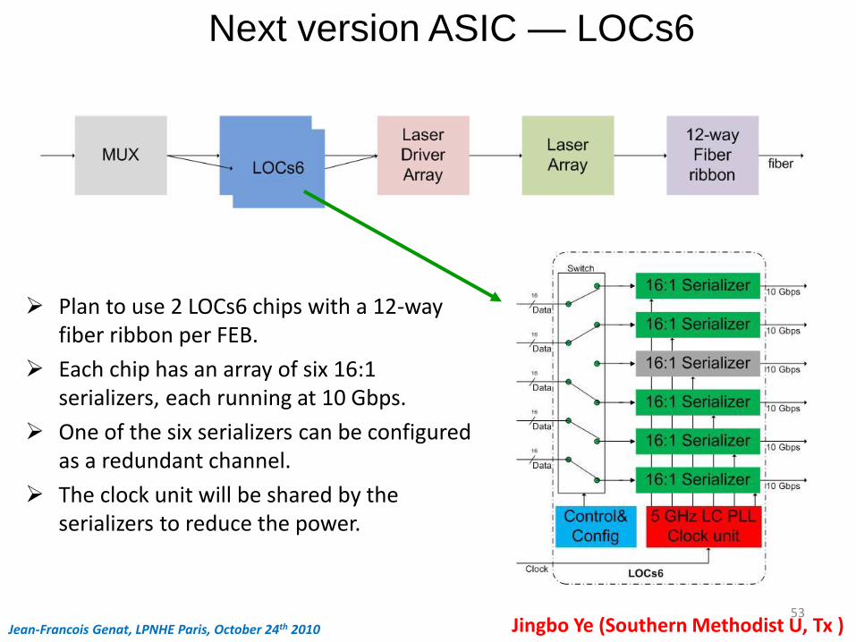
LOC6 project
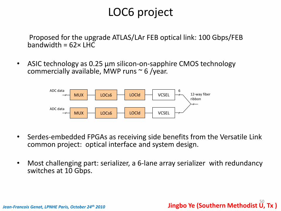
Proposed for the upgrade ATLAS/LAr FEB optical link: 100 Gbps/FEB bandwidth = 62× LHC
• ASIC technology as 0.25 μm silicon-on-sapphire CMOS technology
commercially available, MWP runs ~ 6 /year.
• Serdes-embedded FPGAs as receiving side benefits from the Versatile Link common project: optical interface and system design.
• Most challenging part: serializer, a 6-lane array serializer with redundancy switches at 10 Gbps.
MUX LOCs6 LOCld VCSEL ADC data
MUX LOCs6 LOCld VCSEL ADC data
6 12-way fiber ribbon
Jingbo Ye (Southern Methodist U, Tx ) Jean-Francois Genat, LPNHE Paris, October 24th 2010 50
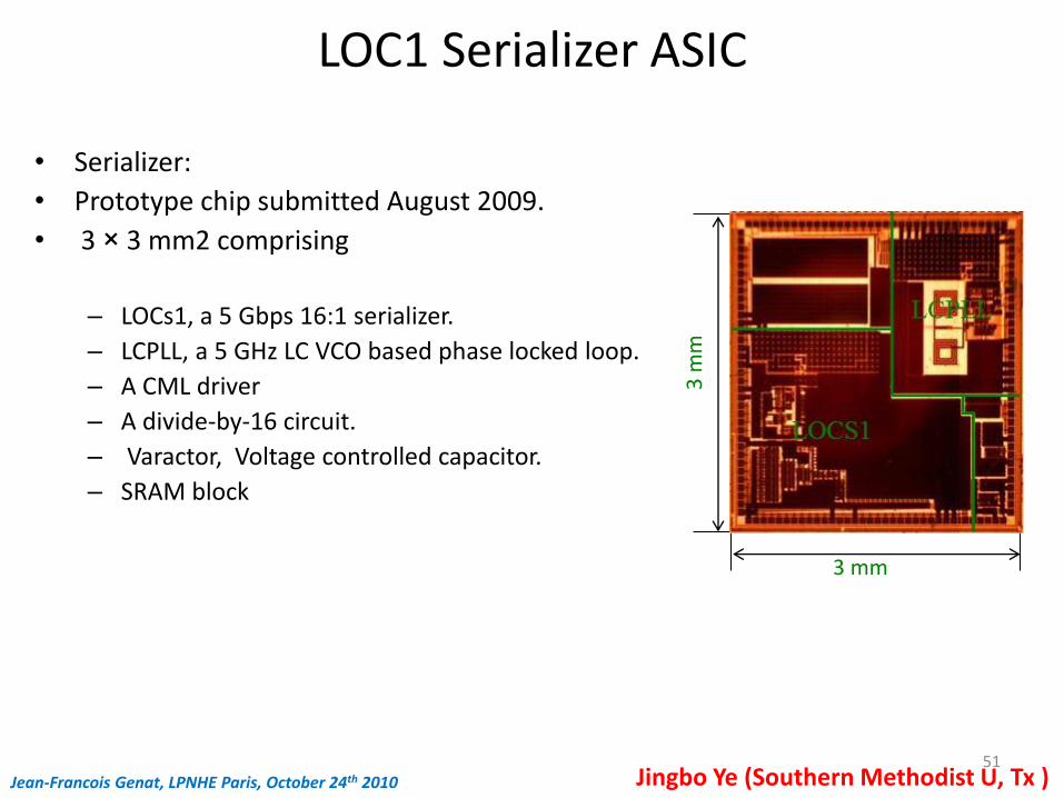
LOC1 Serializer ASIC
• Serializer:
• Prototype chip submitted August 2009.
• 3 × 3 mm2 comprising
– LOCs1, a 5 Gbps 16:1 serializer.
– LCPLL, a 5 GHz LC VCO based phase locked loop.
– A CML driver
– A divide-by-16 circuit.
– Varactor, Voltage controlled capacitor.
– SRAM block
3 mm
3 m
m
Jingbo Ye (Southern Methodist U, Tx ) Jean-Francois Genat, LPNHE Paris, October 24th 2010 51
52
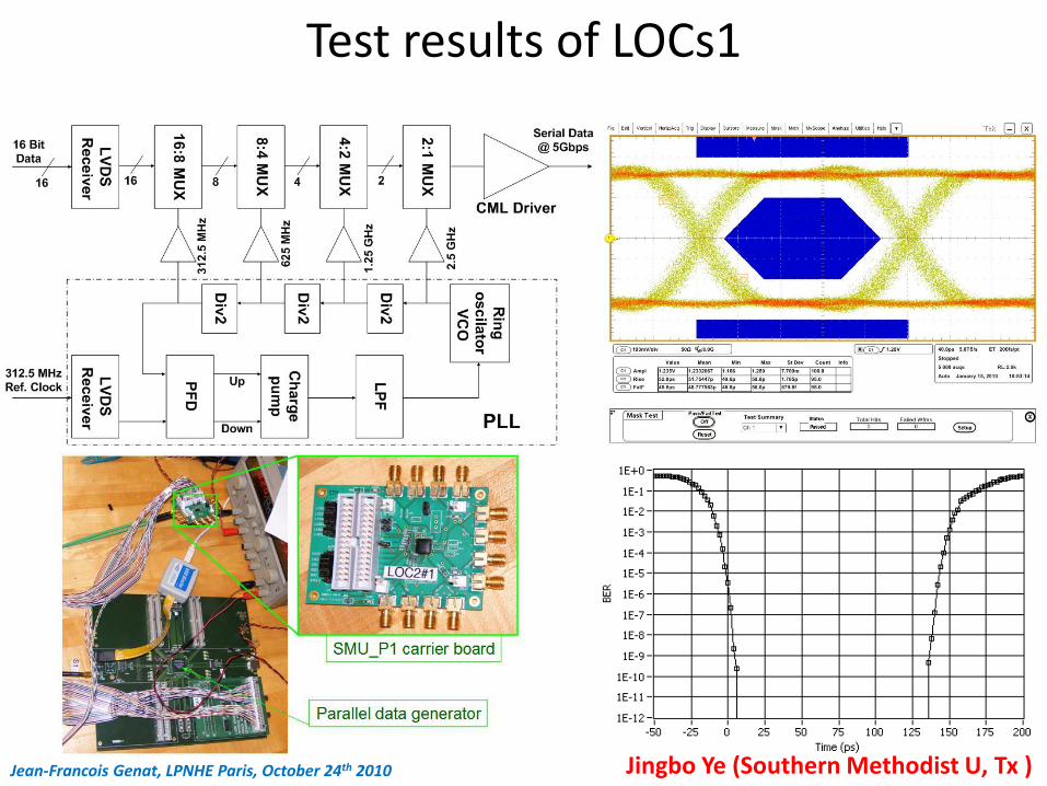
Test results of LOCs1
Jingbo Ye (Southern Methodist U, Tx ) Jean-Francois Genat, LPNHE Paris, October 24th 2010
Next version ASIC — LOCs6
Plan to use 2 LOCs6 chips with a 12-way fiber ribbon per FEB.
Each chip has an array of six 16:1 serializers, each running at 10 Gbps.
One of the six serializers can be configured as a redundant channel.
The clock unit will be shared by the serializers to reduce the power.
Jean-Francois Genat, LPNHE Paris, October 24th 2010 Jingbo Ye (Southern Methodist U, Tx ) 53
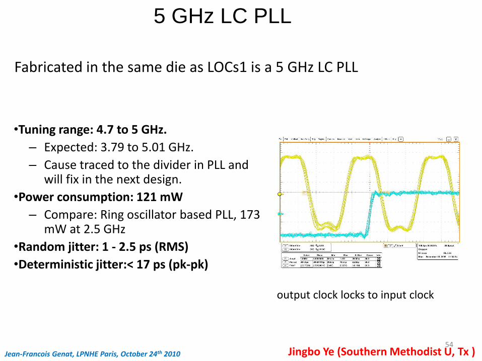
5 GHz LC PLL
output clock locks to input clock
Fabricated in the same die as LOCs1 is a 5 GHz LC PLL
•Tuning range: 4.7 to 5 GHz.
– Expected: 3.79 to 5.01 GHz.
– Cause traced to the divider in PLL and will fix in the next design.
•Power consumption: 121 mW
– Compare: Ring oscillator based PLL, 173 mW at 2.5 GHz
•Random jitter: 1 - 2.5 ps (RMS)
•Deterministic jitter:< 17 ps (pk-pk)
Jean-Francois Genat, LPNHE Paris, October 24th 2010 Jingbo Ye (Southern Methodist U, Tx ) 54
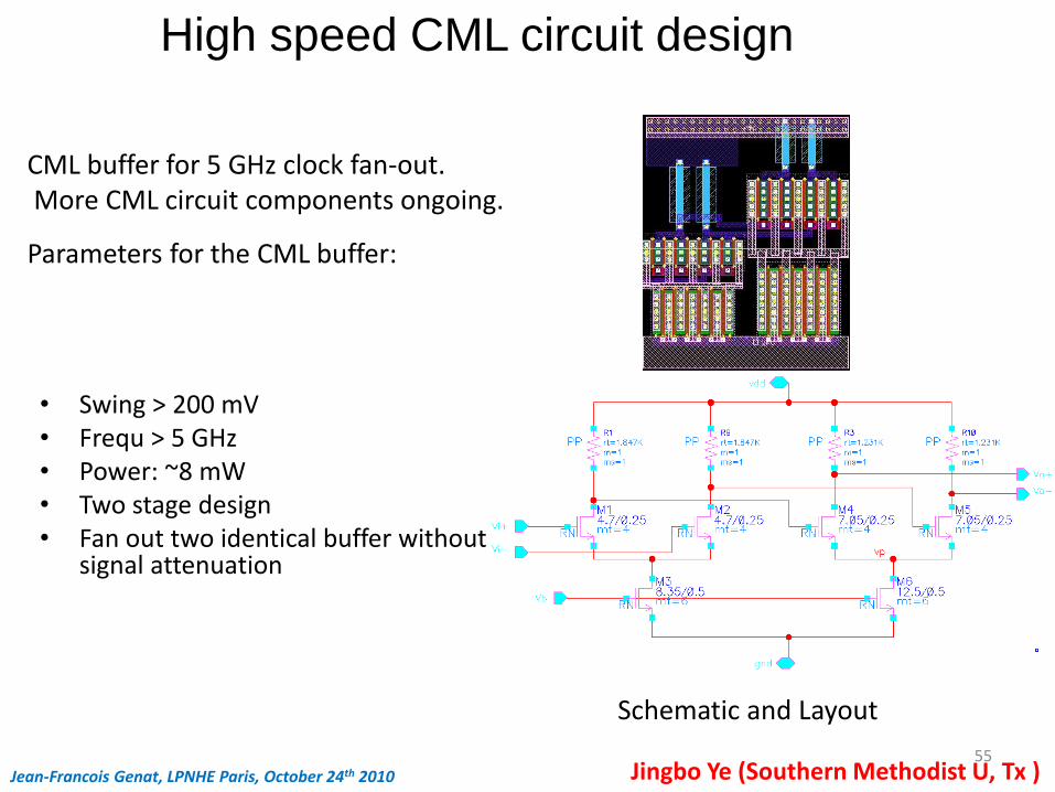
• Swing > 200 mV • Frequ > 5 GHz • Power: ~8 mW • Two stage design • Fan out two identical buffer without
signal attenuation
High speed CML circuit design
CML buffer for 5 GHz clock fan-out. More CML circuit components ongoing.
Parameters for the CML buffer:
Schematic and Layout
Jean-Francois Genat, LPNHE Paris, October 24th 2010 Jingbo Ye (Southern Methodist U, Tx ) 55
Design of LOCs6
As of the LOC1 tests, more needed.
More tests on LOCs1 are still needed
First proton test on LOCs1 produced very good results.
More tests may be needed to study SEE.
Would like to investigate an array laser driver, LOCLD6
Limited by manpower and resource. Need help in the development of the 100 Gbps/board system.
Plans and Summary
Jean-Francois Genat, LPNHE Paris, October 24th 2010 Jingbo Ye (Southern Methodist U, Tx ) 56
Jan Troska (CERN)
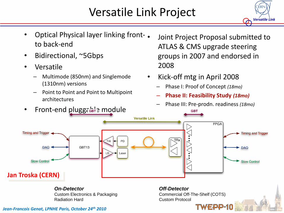
Versatile Link Project
• Optical Physical layer linking front- to back-end
• Bidirectional, ~5Gbps
• Versatile – Multimode (850nm) and Singlemode
(1310nm) versions
– Point to Point and Point to Multipoint architectures
• Front-end pluggable module
• Joint Project Proposal submitted to ATLAS & CMS upgrade steering groups in 2007 and endorsed in 2008
• Kick-off mtg in April 2008 – Phase I: Proof of Concept (18mo)
– Phase II: Feasibility Study (18mo)
– Phase III: Pre-prodn. readiness (18mo)
Versatile Link
On-Detector Custom Electronics & Packaging
Radiation Hard
Off-Detector Commercial Off-The-Shelf (COTS)
Custom Protocol
Jean-Francois Genat, LPNHE Paris, October 24th 2010 57
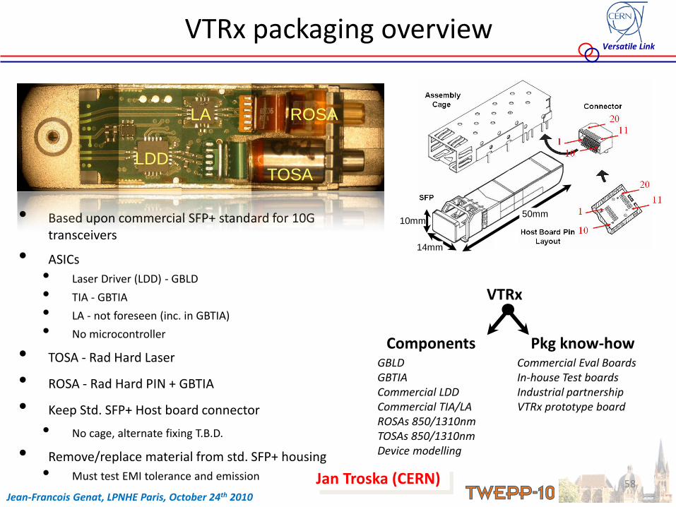
Versatile Link VTRx packaging overview
• Based upon commercial SFP+ standard for 10G transceivers
• ASICs
• Laser Driver (LDD) - GBLD
• TIA - GBTIA
• LA - not foreseen (inc. in GBTIA)
• No microcontroller
• TOSA - Rad Hard Laser
• ROSA - Rad Hard PIN + GBTIA
• Keep Std. SFP+ Host board connector
• No cage, alternate fixing T.B.D.
• Remove/replace material from std. SFP+ housing
• Must test EMI tolerance and emission
LDD
LA
TOSA
ROSA
50mm
14mm
10mm
VTRx
Components Pkg know-how GBLD GBTIA Commercial LDD Commercial TIA/LA ROSAs 850/1310nm TOSAs 850/1310nm Device modelling
Commercial Eval Boards In-house Test boards Industrial partnership VTRx prototype board
Jan Troska (CERN) Jean-Francois Genat, LPNHE Paris, October 24th 2010
58
Versatile Link
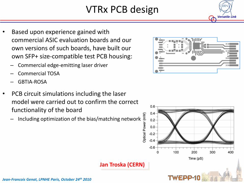
VTRx PCB design
• Based upon experience gained with commercial ASIC evaluation boards and our own versions of such boards, have built our own SFP+ size-compatible test PCB housing:
– Commercial edge-emitting laser driver
– Commercial TOSA
– GBTIA-ROSA
• PCB circuit simulations including the laser model were carried out to confirm the correct functionality of the board
– Including optimization of the bias/matching network
Jan Troska (CERN)
Jean-Francois Genat, LPNHE Paris, October 24th 2010 59
Versatile Link
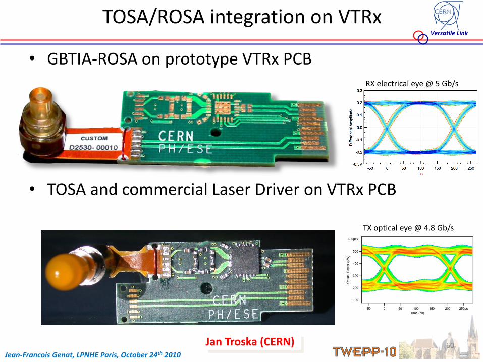
TOSA/ROSA integration on VTRx
• GBTIA-ROSA on prototype VTRx PCB
• TOSA and commercial Laser Driver on VTRx PCB
RX electrical eye @ 5 Gb/s
TX optical eye @ 4.8 Gb/s
Jan Troska (CERN) Jean-Francois Genat, LPNHE Paris, October 24th 2010
60
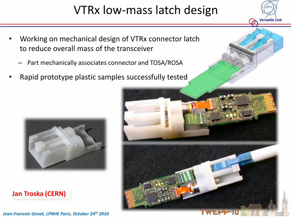
• Working on mechanical design of VTRx connector latch to reduce overall mass of the transceiver
– Part mechanically associates connector and TOSA/ROSA
• Rapid prototype plastic samples successfully tested
Versatile Link
VTRx low-mass latch design
Jan Troska (CERN)
Jean-Francois Genat, LPNHE Paris, October 24th 2010 61
Versatile Link
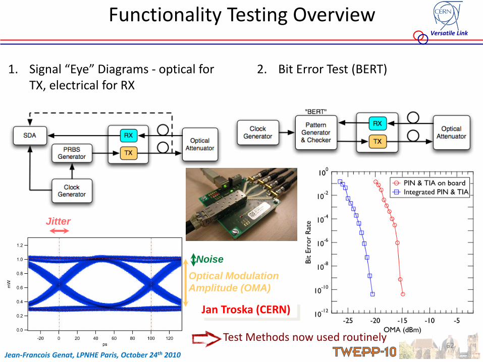
Functionality Testing Overview
1. Signal “Eye” Diagrams - optical for TX, electrical for RX
Jitter
Optical Modulation
Amplitude (OMA)
Noise
Test Methods now used routinely
2. Bit Error Test (BERT)
Jan Troska (CERN)
Jean-Francois Genat, LPNHE Paris, October 24th 2010 62
Versatile Link
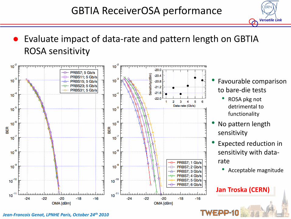
GBTIA ReceiverOSA performance
● Evaluate impact of data-rate and pattern length on GBTIA ROSA sensitivity
• Favourable comparison to bare-die tests • ROSA pkg not
detrimental to functionality
• No pattern length sensitivity
• Expected reduction in sensitivity with data-rate • Acceptable magnitude
Jan Troska (CERN)
Jean-Francois Genat, LPNHE Paris, October 24th 2010 63
Versatile Link
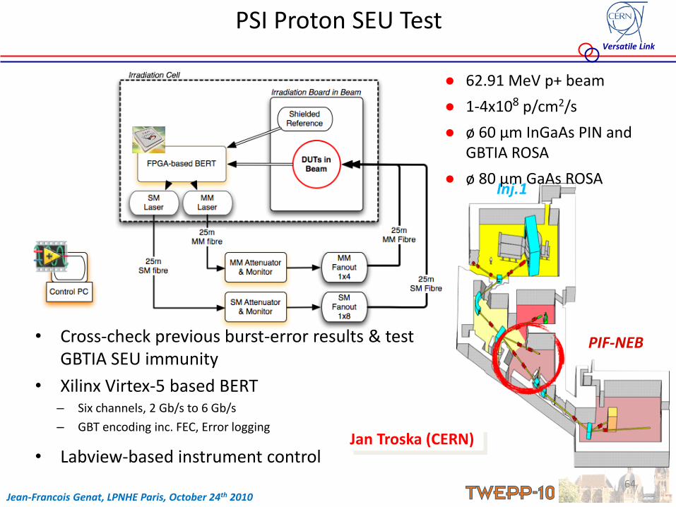
PSI Proton SEU Test
• Cross-check previous burst-error results & test GBTIA SEU immunity
• Xilinx Virtex-5 based BERT – Six channels, 2 Gb/s to 6 Gb/s
– GBT encoding inc. FEC, Error logging
• Labview-based instrument control
PIF-NEB
Inj.1
● 62.91 MeV p+ beam
● 1-4x10⁸ p/cm2/s
● ø 60 µm InGaAs PIN and GBTIA ROSA
● ø 80 µm GaAs ROSA
Jan Troska (CERN)
Jean-Francois Genat, LPNHE Paris, October 24th 2010 64
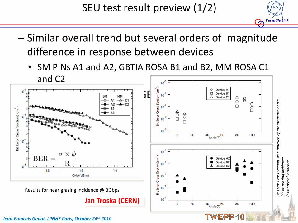
– Similar overall trend but several orders of magnitude difference in response between devices
• SM PINs A1 and A2, GBTIA ROSA B1 and B2, MM ROSA C1 and C2
– Best performance from GBTIA ROSAs (square symbols)
Versatile Link
SEU test result preview (1/2)
Results for near grazing incidence @ 3Gbps
Bit
Err
or
Cro
ss S
ecti
on
as
a f
un
ctio
n o
f th
e in
cid
ence
an
gle
, 9
0 =
= g
razi
ng
inci
den
ce
0 =
= n
orm
al i
nci
den
ce
Jan Troska (CERN)
Jean-Francois Genat, LPNHE Paris, October 24th 2010 65
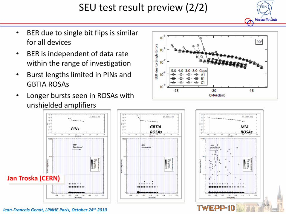
• BER due to single bit flips is similar for all devices
• BER is independent of data rate within the range of investigation
• Burst lengths limited in PINs and GBTIA ROSAs
• Longer bursts seen in ROSAs with unshielded amplifiers
Versatile Link
SEU test result preview (2/2)
PINs GBTIA ROSAs
MM ROSAs
Jan Troska (CERN)
Jean-Francois Genat, LPNHE Paris, October 24th 2010 66
Versatile Link
Summary & future work
• In terms of our Phase II deliverables – Specifications for on-detector components
• Available and under discussion within Versatile link project, soon to be distributed more widely
– Packaging
• In-house development of both PCB and mechanical pkg progressing well
• Successful integration of GBTIA and PIN into ROSA
– Detailed measurements of multiple devices in near future • Defining strategy for future variants (GBLD, TOSA types)
– Functional test methods applied to testing of transmitters and receivers
• Excellent performance of GBTIA ROSA
• Performance limitation of current VTRx design being studied in simulation
– Radiation Testing
• SEU test results compare well with previous results
– Burst errors not observed in GBTIA or high-speed commercial TIA • Pion test carried out, lots of data to analyse
Jan Troska (CERN) Jean-Francois Genat, LPNHE Paris, October 24th 2010
67
xTCA Micro/Advanced Telecommunications
Computing Architecture
Jean-Francois Genat, LPNHE Paris, October 24th 2010 68
LHCb Upgrade
Jean-Francois Genat, LPNHE Paris, October 24th 2010 69
J-P Cachemiche, CPP Marseille
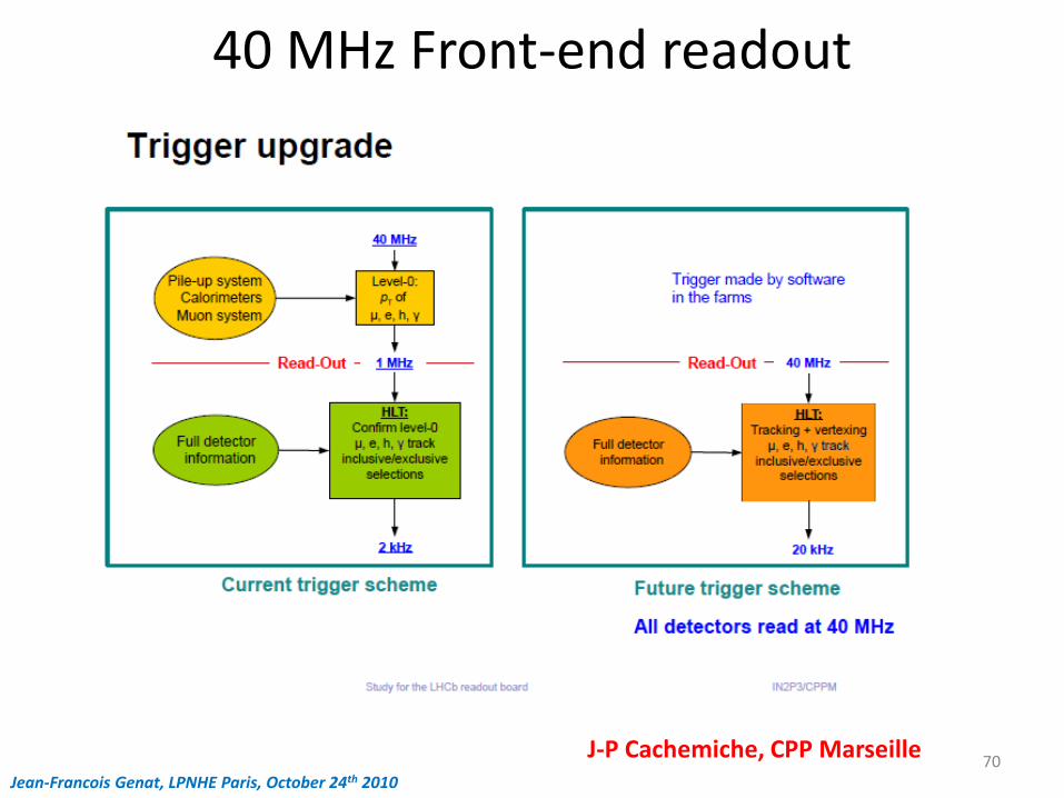
40 MHz Front-end readout
Jean-Francois Genat, LPNHE Paris, October 24th 2010 70
J-P Cachemiche, CPP Marseille
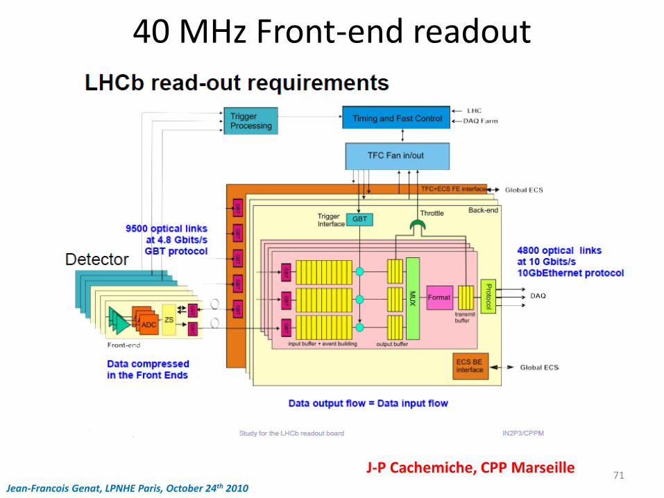
40 MHz Front-end readout
Jean-Francois Genat, LPNHE Paris, October 24th 2010 71
J-P Cachemiche, CPP Marseille
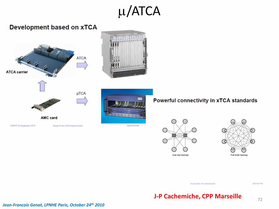
m/ATCA
Jean-Francois Genat, LPNHE Paris, October 24th 2010 72
J-P Cachemiche, CPP Marseille
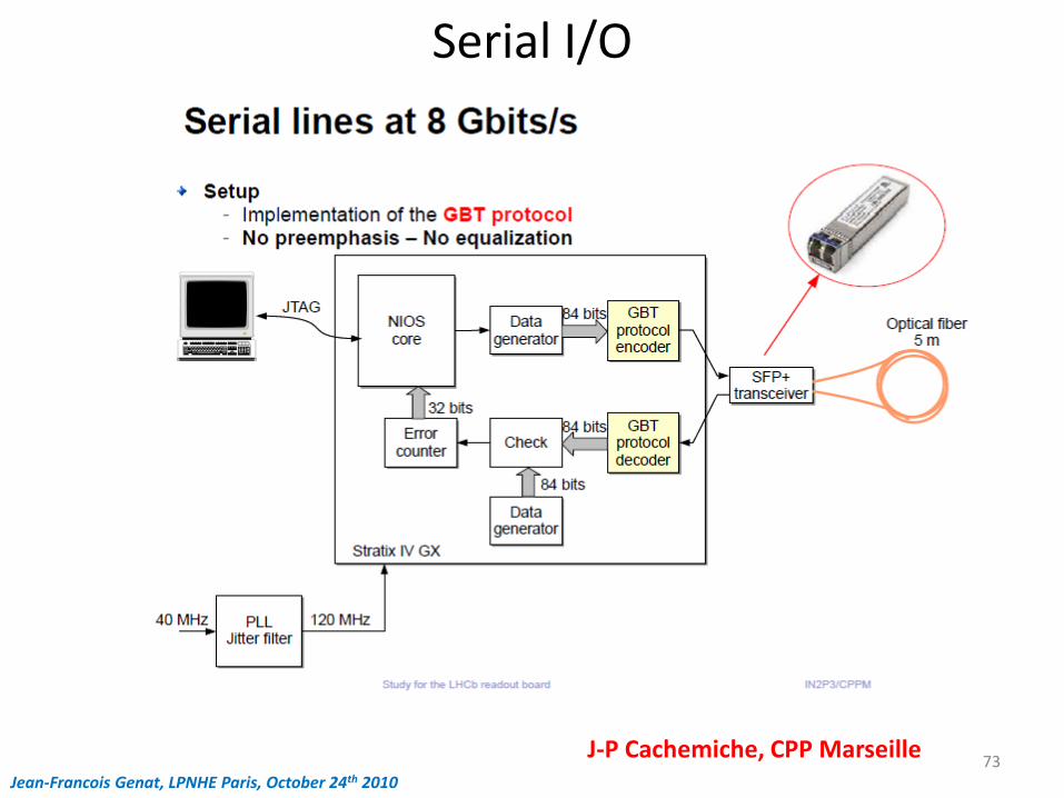
Serial I/O
Jean-Francois Genat, LPNHE Paris, October 24th 2010 73
J-P Cachemiche, CPP Marseille
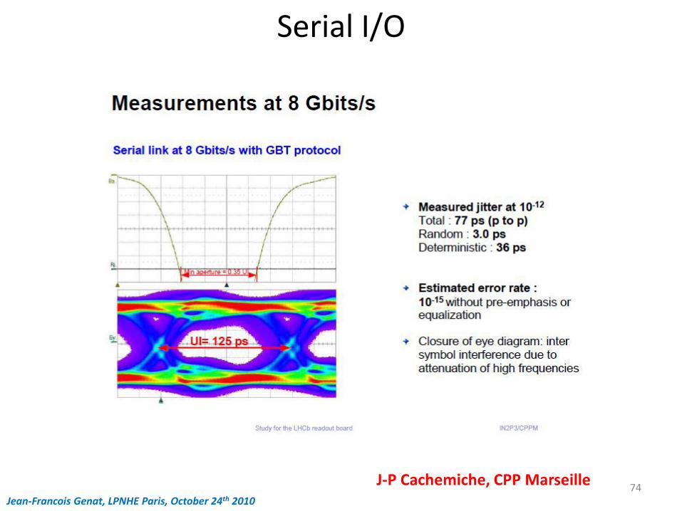
Serial I/O
Jean-Francois Genat, LPNHE Paris, October 24th 2010 74
J-P Cachemiche, CPP Marseille
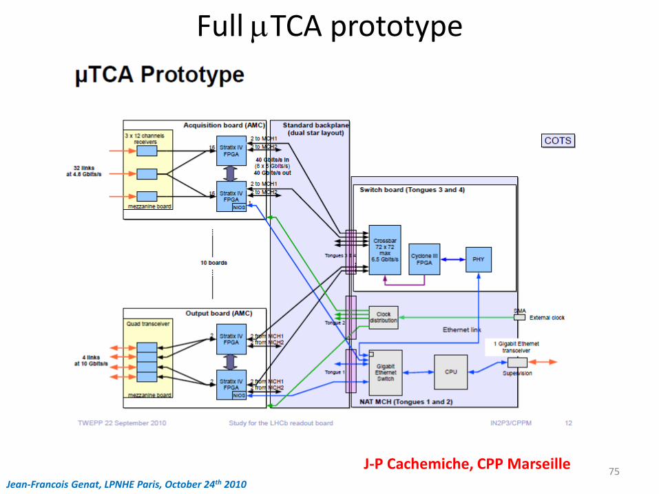
Full mTCA prototype
Jean-Francois Genat, LPNHE Paris, October 24th 2010 75
J-P Cachemiche, CPP Marseille
xTCA CPP Marseille
Jean-Francois Genat, LPNHE Paris, October 24th 2010 76
J-P Cachemiche, CPP Marseille
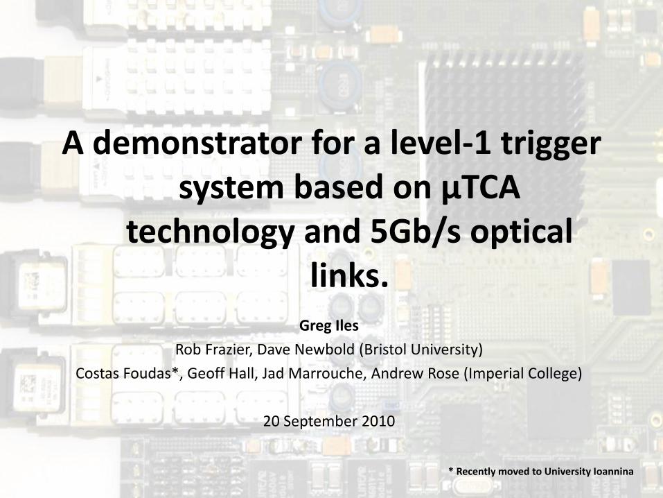
A demonstrator for a level-1 trigger system based on μTCA
technology and 5Gb/s optical links.
Greg Iles
Rob Frazier, Dave Newbold (Bristol University)
Costas Foudas*, Geoff Hall, Jad Marrouche, Andrew Rose (Imperial College)
20 September 2010
* Recently moved to University Ioannina
New Interconnect Technologies
Jean-Francois Genat, LPNHE Paris, October 24th 2010 78
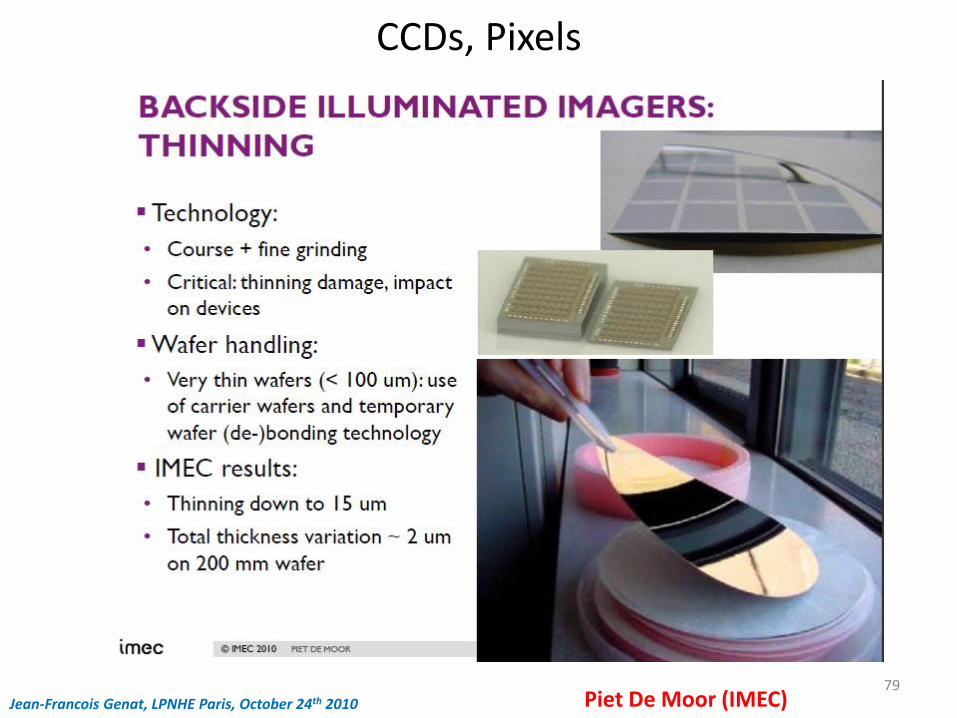
CCDs, Pixels
Jean-Francois Genat, LPNHE Paris, October 24th 2010 Piet De Moor (IMEC) 79
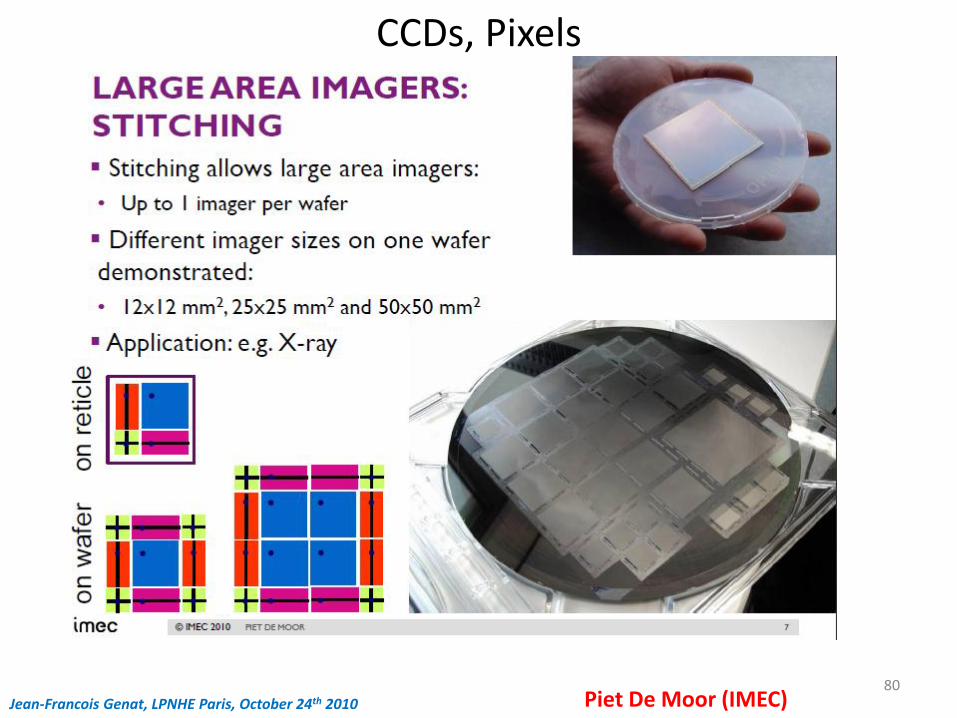
CCDs, Pixels
Jean-Francois Genat, LPNHE Paris, October 24th 2010 Piet De Moor (IMEC) 80
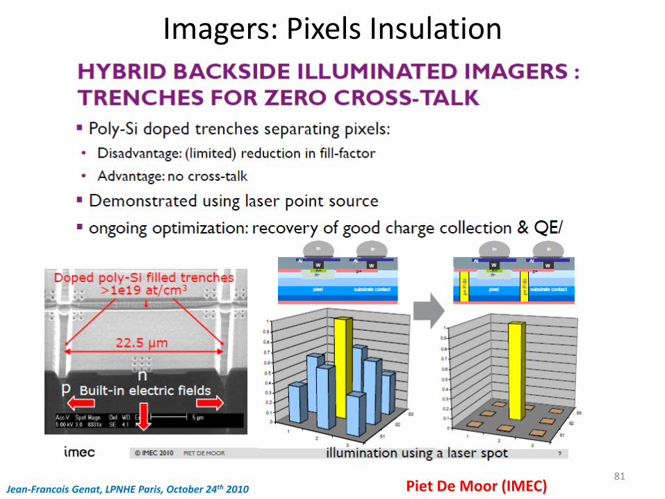
Imagers: Pixels Insulation
Jean-Francois Genat, LPNHE Paris, October 24th 2010 Piet De Moor (IMEC) 81
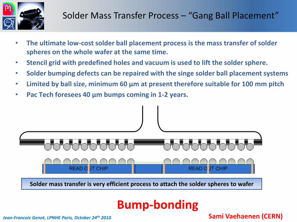
Solder Mass Transfer Process – “Gang Ball Placement”
• The ultimate low-cost solder ball placement process is the mass transfer of solder spheres on the whole wafer at the same time.
• Stencil grid with predefined holes and vacuum is used to lift the solder sphere.
• Solder bumping defects can be repaired with the singe solder ball placement systems
• Limited by ball size, minimum 60 µm at present therefore suitable for 100 mm pitch
• Pac Tech foresees 40 µm bumps coming in 1-2 years.
Solder mass transfer is very efficient process to attach the solder spheres to wafer
Sami Vaehaenen (CERN) Jean-Francois Genat, LPNHE Paris, October 24th 2010
Bump-bonding
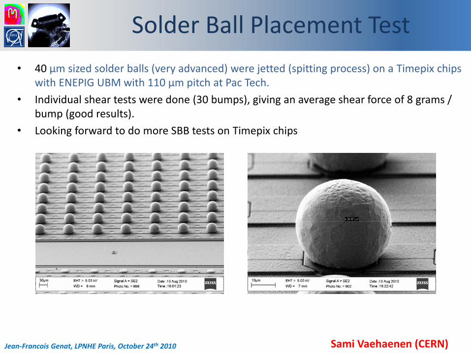
Solder Ball Placement Test
• 40 µm sized solder balls (very advanced) were jetted (spitting process) on a Timepix chips with ENEPIG UBM with 110 µm pitch at Pac Tech.
• Individual shear tests were done (30 bumps), giving an average shear force of 8 grams / bump (good results).
• Looking forward to do more SBB tests on Timepix chips
Jean-Francois Genat, LPNHE Paris, October 24th 2010 Sami Vaehaenen (CERN)
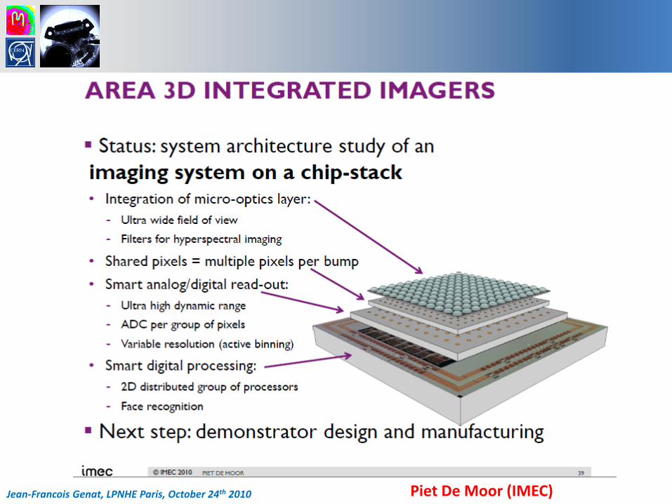
Jean-Francois Genat, LPNHE Paris, October 24th 2010 Piet De Moor (IMEC)
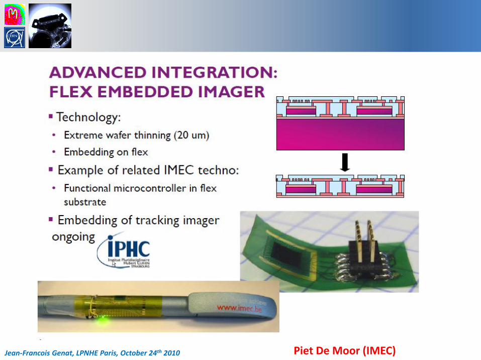
Jean-Francois Genat, LPNHE Paris, October 24th 2010 Piet De Moor (IMEC)
Piet De Moor (IMEC) Jean-Francois Genat, LPNHE Paris, October 24th 2010
Parallel Computing
Jean-Francois Genat, LPNHE Paris, October 24th 2010 87
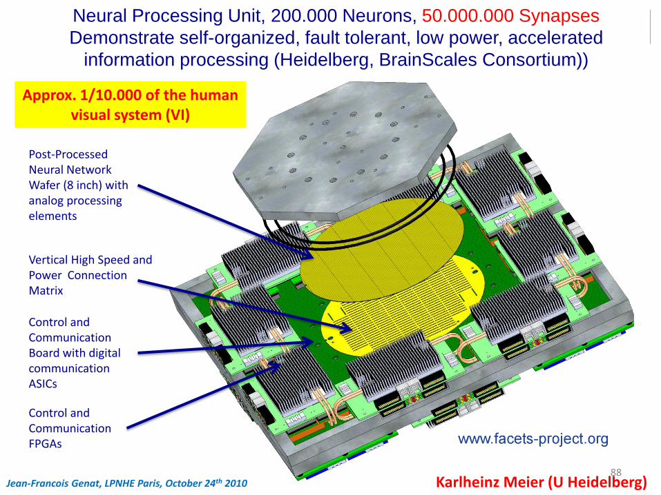
Neural Processing Unit, 200.000 Neurons, 50.000.000 Synapses
Demonstrate self-organized, fault tolerant, low power, accelerated
information processing (Heidelberg, BrainScales Consortium))
Post-Processed Neural Network Wafer (8 inch) with analog processing elements
Vertical High Speed and Power Connection Matrix
Control and Communication FPGAs
Control and Communication Board with digital communication ASICs
Approx. 1/10.000 of the human visual system (VI)
Karlheinz Meier (U Heidelberg)
Jean-Francois Genat, LPNHE Paris, October 24th 2010
Jean-Francois Genat, LPNHE Paris, October 24th 2010 88
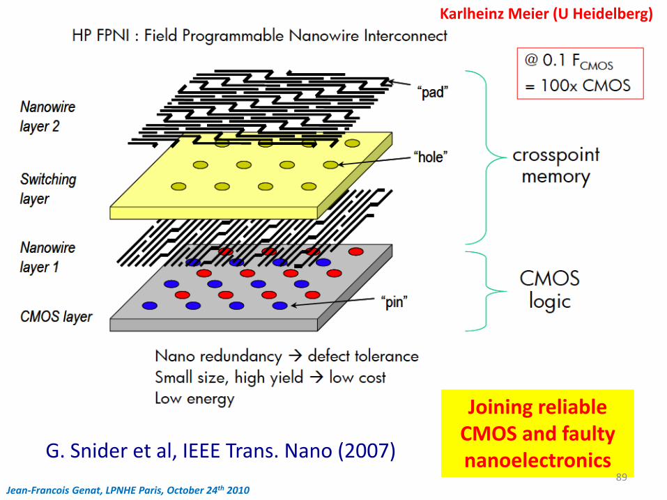
G. Snider et al, IEEE Trans. Nano (2007)
Joining reliable CMOS and faulty nanoelectronics
Karlheinz Meier (U Heidelberg)
Jean-Francois Genat, LPNHE Paris, October 24th 2010 89
Radiation Hardness
Jean-Francois Genat, LPNHE Paris, October 24th 2010 90
Radiation Hardening for Space Applications
Dedicated processes for space are not affordable any more SOI is sometimes used
Low SEU rates, latch-up free, some concerns on TID SOI is less readily available, analogue IPs need to be re-developed
Total Ionising Dose (TID) Most space missions are limited to 100 krad dose, and in 180 nm or
below, TID protection might be limited to e.g. screening of (commercial) library cells, elimination of certain transistor types
Some long duration, deep space missions are in the Mrad domain, requiring mitigation e.g. by special transistor geometries (ELT), guard rings or derating
Single Event Latch-Up (SEL) Horizontal: mitigation in layout, e.g. guard rings Vertical: thickness of the epitaxial layer, deep n-well
Single Event Effects (SEE) by Transient and Upset (SET, SEU) Spatial or temporal redundancy Mitigation by design of library cells or in logic design see below
Roland Weigand (ESA)
Jean-Francois Genat, LPNHE Paris, October 24th 2010 91
Jean-Francois Genat, LPNHE Paris, October 24th 2010 Ashley Greenall (U Liverpool)
ATLAS Silicon detectors upgrade
92
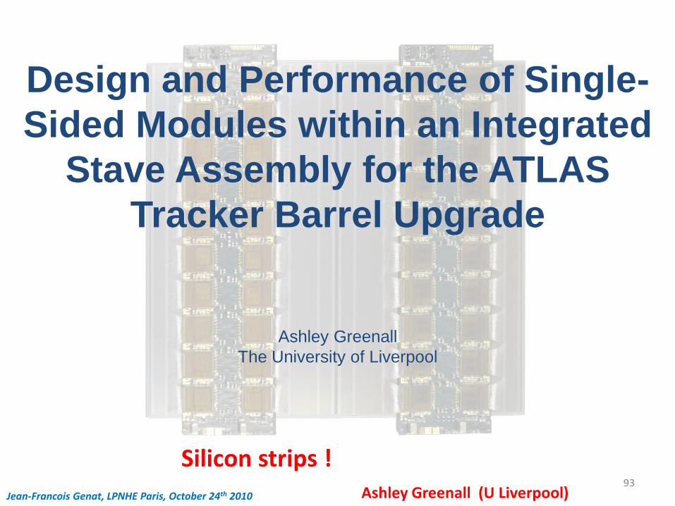
Design and Performance of Single-
Sided Modules within an Integrated
Stave Assembly for the ATLAS
Tracker Barrel Upgrade
Ashley Greenall
The University of Liverpool
Silicon strips !
Jean-Francois Genat, LPNHE Paris, October 24th 2010 Ashley Greenall (U Liverpool) 93
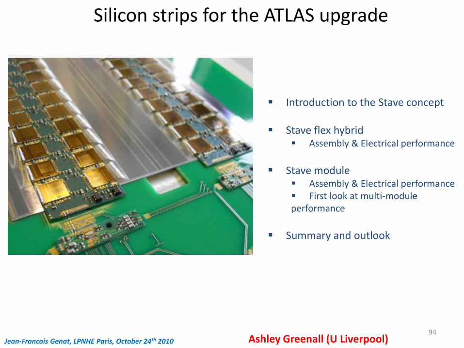
Introduction to the Stave concept
Stave flex hybrid Assembly & Electrical performance
Stave module
Assembly & Electrical performance First look at multi-module performance
Summary and outlook
Jean-Francois Genat, LPNHE Paris, October 24th 2010 Ashley Greenall (U Liverpool)
Silicon strips for the ATLAS upgrade
94
ATLAS Tracker Upgrade Week, 23rd-27th Feb 09
Have successfully demonstrated the design and build of a substrate-less module
Issues of yield and volume production being addressed from the outset
Individually, serially powered modules, have been shown to perform excellently
First tests of a serially powered multi-module short stave (Stavelet) are very promising
Stavelet tests are ongoing (with future plans for a DCDC powered variant)
Intention is to build a module using the new shield-less hybrids (reduced material)
Longer term, the plan is to build a full size double-sided Stave composed of 24 modules
Jean-Francois Genat, LPNHE Paris, October 24th 2010 Ashley Greenall (U Liverpool)
Silicon strips for the ATLAS upgrade
95
Jean-Francois Genat, LPNHE Paris, October 24th 2010 Michael Beimforde (MPI Munich)
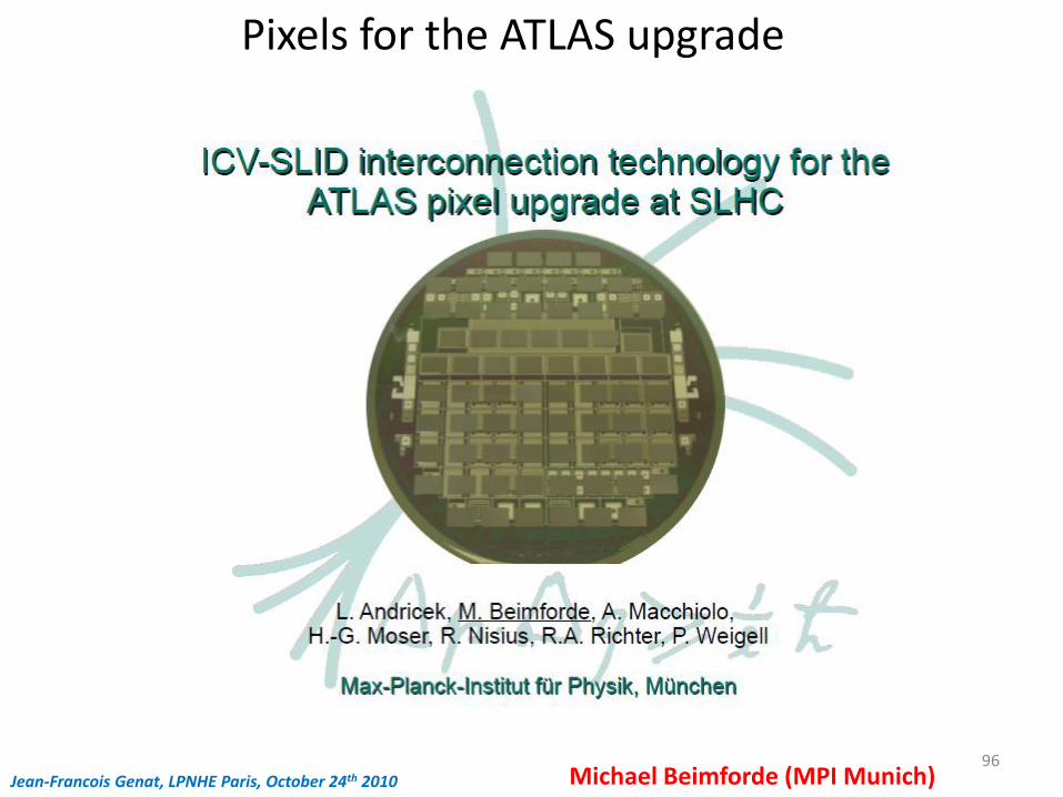
Pixels for the ATLAS upgrade
96
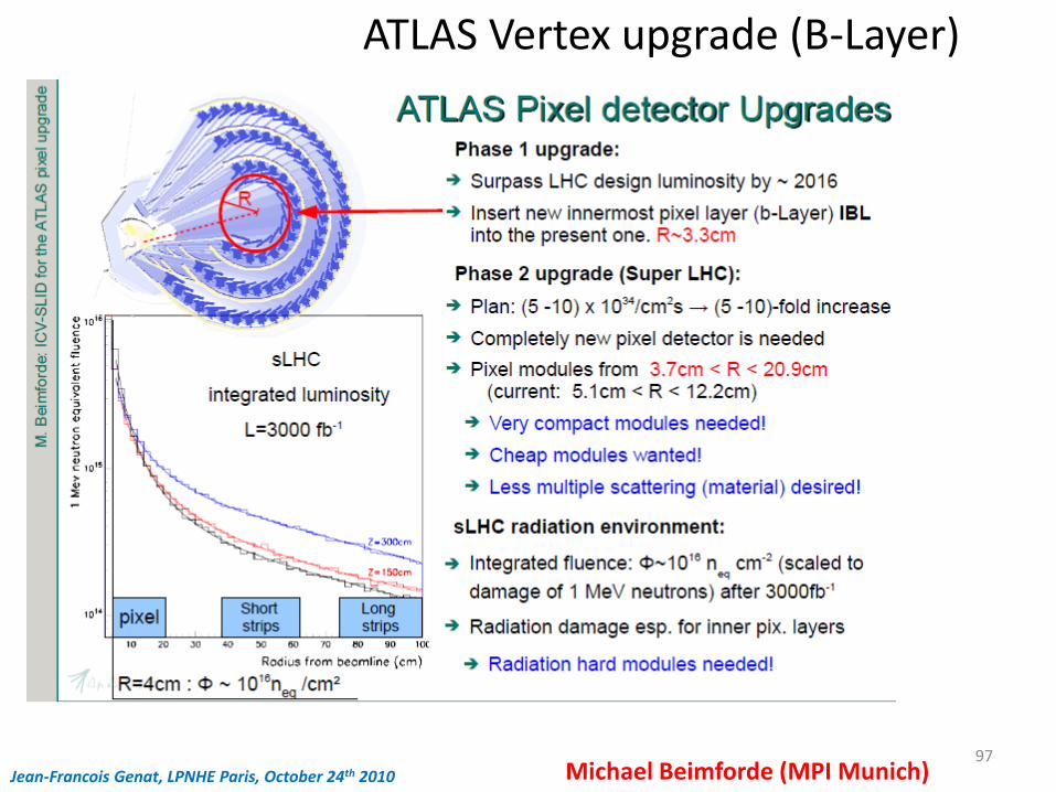
Jean-Francois Genat, LPNHE Paris, October 24th 2010 Michael Beimforde (MPI Munich)
ATLAS Vertex upgrade (B-Layer)
97
Jean-Francois Genat, LPNHE Paris, October 24th 2010 Michael Beimforde (MPI Munich)
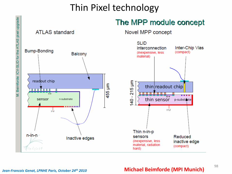
Thin Pixel technology
98
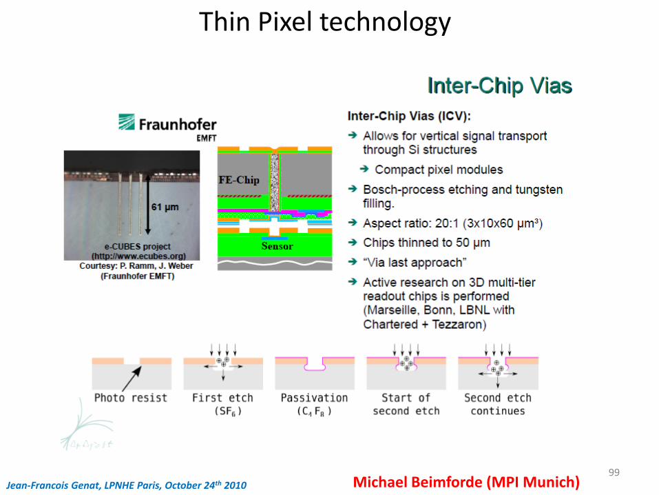
Jean-Francois Genat, LPNHE Paris, October 24th 2010 Michael Beimforde (MPI Munich)
Thin Pixel technology
99
Triggers
Jean-Francois Genat, LPNHE Paris, October 24th 2010 100
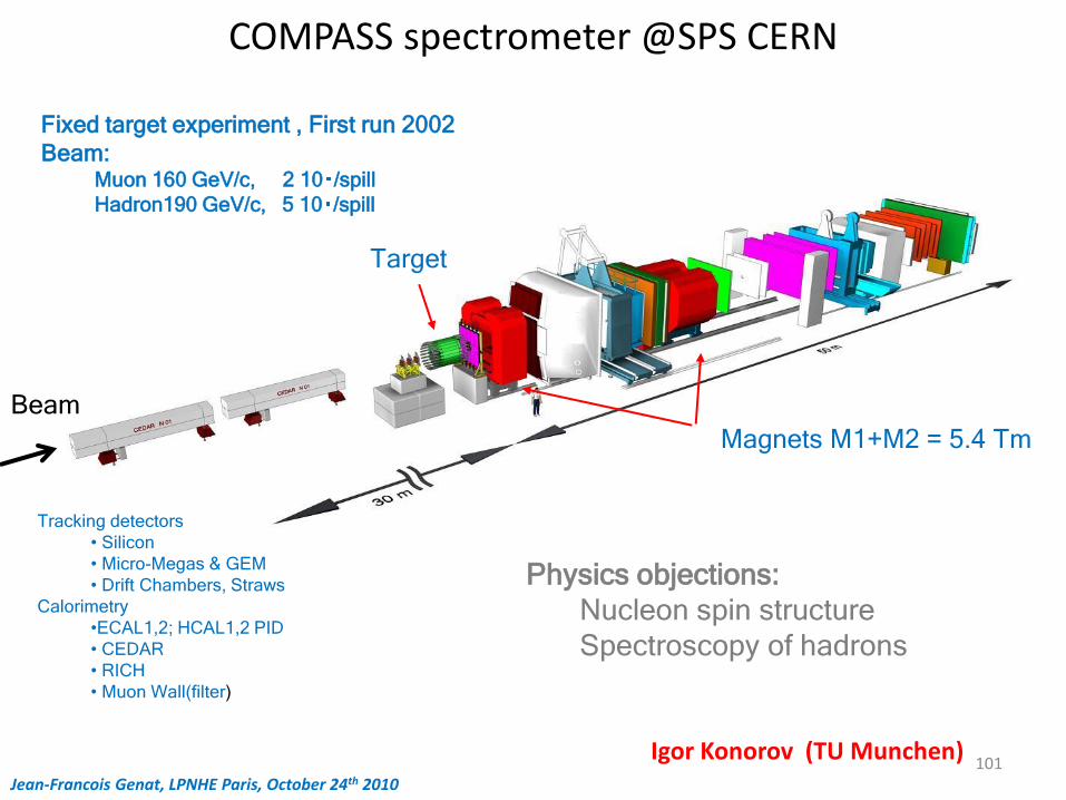
COMPASS spectrometer @SPS CERN
Игорь Коноров
101
Target
Magnets M1+M2 = 5.4 Tm
Fixed target experiment , First run 2002
Beam: Muon 160 GeV/c, 2 10 /spill
Hadron190 GeV/c, 5 10 /spill
Tracking detectors
• Silicon
• Micro-Megas & GEM
• Drift Chambers, Straws
Calorimetry
•ECAL1,2; HCAL1,2 PID
• CEDAR
• RICH
• Muon Wall(filter)
Physics objections:
Nucleon spin structure
Spectroscopy of hadrons
Beam
Jean-Francois Genat, LPNHE Paris, October 24th 2010
Igor Konorov (TU Munchen)
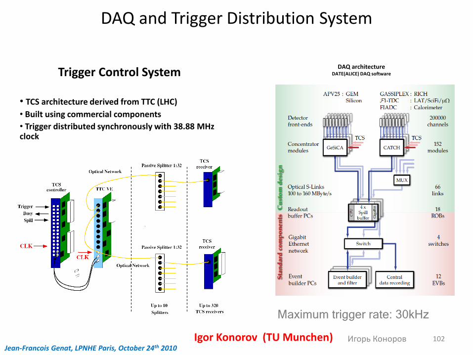
DAQ and Trigger Distribution System
DAQ architecture DATE(ALICE) DAQ software Trigger Control System
• TCS architecture derived from TTC (LHC)
• Built using commercial components
• Trigger distributed synchronously with 38.88 MHz clock
Игорь Коноров 102
Maximum trigger rate: 30kHz
Jean-Francois Genat, LPNHE Paris, October 24th 2010 Igor Konorov (TU Munchen)
TDC based Trigger Logic in FPGA
Motivation: Currently COMPASS trigger electronics is based mostly on NIM modules.
Substitute NIM logic with flexible FPGA based electronics
What is the Trigger logic ? Interconnection of simple logical components: OR, INV, AND
How a Digital Trigger Logic look like: – Synchronous pipeline architecture – predictable behavior
– Convert analog Timing Information into DIGITs (TDC in FPGA)
– Unified interface : LEMO cable substitutd by FIFO like interface with TDC information
– Library components: NxOR, Nx(N)AND
How to create an FPGA firmware – Interconnections Described in Top level VHDL file
– User creates schematic(net list)
– Software tools generate TOP level VHDL file
Goal: provide a possibility to create a Complex Trigger Logic without a FPGA/VHDL knowledge
Игорь Коноров
103 Jean-Francois Genat, LPNHE Paris, October 24th 2010
Igor Konorov (TU Munchen)
Trigger logic components
• TDC
• Programmable delays
• AND, OR, NAND with programmable coincidence window(GATE) and master signal
• Time calibration – automatic scanning signal timing
• Monitoring
• DAQ interface – no need for splitting signals to TDCs
• Inter module interface for scaling up the system
Software • GUI for creating trigger logic schematic
• Software for generation VHDL code and project files
• Standard Xilinx tools to be used for implementation
• No special knowledge required for using the system
Jean-Francois Genat, LPNHE Paris, October 24th 2010 Igor Konorov (TU Munchen)
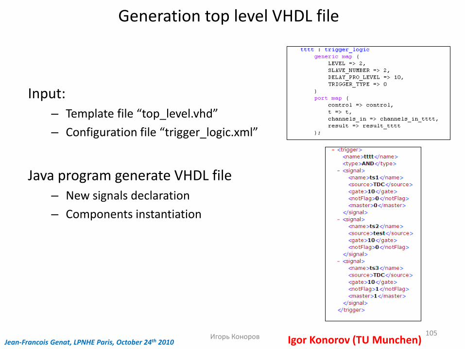
Generation top level VHDL file
Input: – Template file “top_level.vhd”
– Configuration file “trigger_logic.xml”
Java program generate VHDL file – New signals declaration
– Components instantiation
Игорь Коноров 105 Jean-Francois Genat, LPNHE Paris, October 24th 2010 Igor Konorov (TU Munchen)

LHC Status and Plans
Jean-Francois Genat, LPNHE Paris, October 24th 2010 106
Physics at LHC
Patrick Puzo (LAL Orsay)
Jean-Francois Genat, LPNHE Paris, October 24th 2010 107
Physics at LHC/ILC needs…
Patrick Puzo (LAL Orsay)
Jean-Francois Genat, LPNHE Paris, October 24th 2010 108
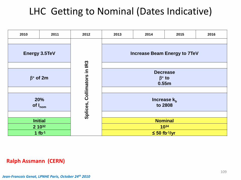
LHC Getting to Nominal (Dates Indicative)
109
2010 2011 2012 2013 2014 2015 2016
Energy 3.5TeV
Sp
lic
es
, C
oll
ima
tors
in
IR
3
Increase Beam Energy to 7TeV
of 2m
Decrease
to
0.55m
20%
of Inom
Increase kb
to 2808
Initial Nominal
2 1032 1034
1 fb-1 ≤ 50 fb-1/yr
Ralph Assmann (CERN)
Jean-Francois Genat, LPNHE Paris, October 24th 2010
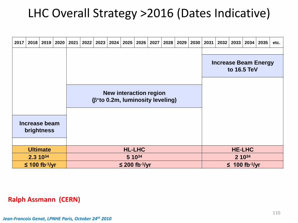
LHC Overall Strategy >2016 (Dates Indicative)
110
2017 2018 2019 2020 2021 2022 2023 2024 2025 2026 2027 2028 2029 2030 2031 2032 2033 2034 2035 etc.
Increase Beam Energy
to 16.5 TeV
New interaction region
(to 0.2m, luminosity leveling)
Increase beam
brightness
Ultimate HL-LHC HE-LHC
2.3 1034 5 1034 2 1034
≤ 100 fb-1/yr ≤ 200 fb-1/yr ≤ 100 fb-1/yr
Ralph Assmann (CERN)
Jean-Francois Genat, LPNHE Paris, October 24th 2010
111
2035…

112
Thanks !!!