Embed Size (px)
Citation preview

TC58CYG0S3HxAIx
©2016 TOSHIBA CORPORATION 2016-11-08C 0
TOSHIBA Serial Interface NAND Technical Data Sheet
Rev. 1.1 2016 – 11 –08
TOSHIBA Storage & Electronic Devices Solutions
Memory Division
TC58CYG0S3HxAIx
©2016 TOSHIBA CORPORATION 2016-11-08C 1
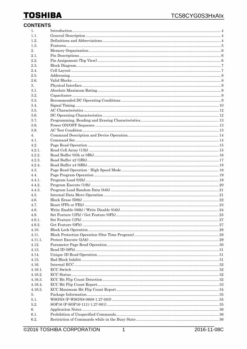
CONTENTS 1. Introduction .............................................................................................................................................. 4 1.1. General Description ................................................................................................................................. 4 1.2. Definitions and Abbreviations ................................................................................................................. 4 1.3. Features .................................................................................................................................................... 5 2. Memory Organization .............................................................................................................................. 6 2.1. Pin Descriptions ....................................................................................................................................... 6 2.2. Pin Assignment (Top View) ...................................................................................................................... 6 2.3. Block Diagram .......................................................................................................................................... 7 2.4. Cell Layout ............................................................................................................................................... 7 2.5. Addressing ................................................................................................................................................ 8 2.6. Valid Blocks .............................................................................................................................................. 8 3. Physical Interface..................................................................................................................................... 9 3.1. Absolute Maximum Rating ...................................................................................................................... 9 3.2. Capacitance .............................................................................................................................................. 9 3.3. Recommended DC Operating Conditions ............................................................................................... 9 3.4. Signal Timing ......................................................................................................................................... 10 3.5. AC Characteristics ................................................................................................................................. 12 3.6. DC Operating Characteristics ............................................................................................................... 12 3.7. Programming, Reading and Erasing Characteristics ........................................................................... 13 3.8. Power ON/OFF Sequence ...................................................................................................................... 13 3.9. AC Test Condition .................................................................................................................................. 13 4. Command Description and Device Operation ....................................................................................... 14 4.1. Command Set ......................................................................................................................................... 14 4.2. Page Read Operation ............................................................................................................................. 15 4.2.1. Read Cell Array (13h) ............................................................................................................................ 15 4.2.2. Read Buffer (03h or 0Bh) ....................................................................................................................... 16 4.2.3. Read Buffer x2 (3Bh).............................................................................................................................. 17 4.2.4. Read Buffer x4 (6Bh).............................................................................................................................. 18 4.3. Page Read Operation - High Speed Mode ............................................................................................. 18 4.4. Page Program Operation ....................................................................................................................... 19 4.4.1. Program Load (02h) ............................................................................................................................... 19 4.4.2. Program Execute (10h) .......................................................................................................................... 20 4.4.3. Program Load Random Data (84h) ....................................................................................................... 21 4.5. Internal Data Move Operation .............................................................................................................. 21 4.6. Block Erase (D8h) .................................................................................................................................. 22 4.7. Reset (FFh or FEh) ................................................................................................................................ 23 4.8. Write Enable (06h) / Write Disable (04h) .............................................................................................. 24 4.9. Set Feature (1Fh) / Get Feature (0Fh) .................................................................................................. 25 4.9.1. Set Feature (1Fh) ................................................................................................................................... 27 4.9.2. Get Feature (0Fh) .................................................................................................................................. 27 4.10. Block Lock Operation ............................................................................................................................. 28 4.11. Block Protection Operation (One Time Program) ................................................................................. 28 4.11.1. Protect Execute (2Ah) ............................................................................................................................ 29 4.12. Parameter Page Read Operation ........................................................................................................... 30 4.13. Read ID (9Fh) ......................................................................................................................................... 31 4.14. Unique ID Read Operation .................................................................................................................... 31 4.15. Bad Block Inhibit ................................................................................................................................... 31 4.16. Internal ECC .......................................................................................................................................... 32 4.16.1. ECC Switch ............................................................................................................................................ 32 4.16.2. ECC Status ............................................................................................................................................. 32 4.16.3. ECC Bit Flip Count Detection ............................................................................................................... 32 4.16.4. ECC Bit Flip Count Report .................................................................................................................... 33 4.16.5. ECC Maximum Bit Flip Count Report .................................................................................................. 34 5. Package Information .............................................................................................................................. 35 5.1. WSON8 (P-WSON8-0608-1.27-003) ...................................................................................................... 35 5.2. SOP16 (P-SOP16-1111-1.27-001) ........................................................................................................... 35 6. Application Notes ................................................................................................................................... 36 6.1. Prohibition of Unspecified Commands .................................................................................................. 36 6.2. Restriction of Commands while in the Busy State ............................................................................... 36

TC58CYG0S3HxAIx
©2016 TOSHIBA CORPORATION 2016-11-08C 2
6.3. Addressing for Page Program Operation .............................................................................................. 36 6.4. Several Programming Cycles on the Same Page (Partial Page Program)........................................... 36 6.5. Power Off Timing ................................................................................................................................... 37 6.6. Invalid Blocks ......................................................................................................................................... 37 6.7. Failure Phenomena ................................................................................................................................ 38 6.8. Reliability Guidance .............................................................................................................................. 39 7. Revision History ..................................................................................................................................... 40 RESTRICTIONS ON PRODUCT USE .................................................................................................................... 41

TC58CYG0S3HxAIx
©2016 TOSHIBA CORPORATION 2016-11-08C 3
LIST of FIGURES Figure 1. WSON8 Pin Assignment (Top View) .......................................................................................................... 6 Figure 2. SOP16 Pin Assignment (Top View) ............................................................................................................ 6 Figure 3. Block Diagram ............................................................................................................................................ 7 Figure 4. Cell Layout .................................................................................................................................................. 7 Figure 5. Addressing ................................................................................................................................................... 8 Figure 6. SPI Timing ................................................................................................................................................ 10 Figure 7. Serial Input Timing .................................................................................................................................. 10 Figure 8. Serial Output Timing ............................................................................................................................... 10 Figure 9. Hold Timing .............................................................................................................................................. 11 Figure 10. WP Timing (Example) ............................................................................................................................ 11 Figure 11. Power ON/OFF Sequence ....................................................................................................................... 13 Figure 12. Page Read from Cell Array to Buffer ..................................................................................................... 15 Figure 13. Page Read from Buffer Timing .............................................................................................................. 16 Figure 14. Page Read from Buffer x2 Timing .......................................................................................................... 17 Figure 15. Page Read from Buffer x4 Timing .......................................................................................................... 18 Figure 16. Program Load ......................................................................................................................................... 19 Figure 17. Program Execute Timing........................................................................................................................ 20 Figure 18. Program Load Random Data Timing ..................................................................................................... 21 Figure 19. Block Erase Timing ................................................................................................................................ 22 Figure 20. Reset Timing ........................................................................................................................................... 23 Figure 21. Write Enable ........................................................................................................................................... 24 Figure 22. Write Disable Timing.............................................................................................................................. 24 Figure 23. Set Feature Timing ................................................................................................................................. 27 Figure 24. Get Feature Timing ................................................................................................................................ 27 Figure 25. Protect Execute Timing .......................................................................................................................... 29 Figure 26. Read ID Timing....................................................................................................................................... 31
LIST of TABLES
Table 1 Pin Descriptions .......................................................................................................................................... 6 Table 2 Valid Blocks ................................................................................................................................................. 8 Table 3 Absolute Maximum Rating ......................................................................................................................... 9 Table 4 Capacitance (TOPR = 25℃, f = 1MHz) ......................................................................................................... 9 Table 5 Recommended DC Operating Condition .................................................................................................... 9 Table 6 AC Characteristics (TOPR = -40 to 85℃, VCC = 1.7 to 1.95V) ................................................................. 12 Table 7 DC & Operating Characteristics (TOPR = -40 to 85℃, VCC = 1.7 to 1.95V) ........................................... 12 Table 8 Programming, Reading and Erasing Characteristics (TOPR = -40 to 85℃, VCC = 1.7 to 1.95V)........... 13 Table 9 Power on Timing ....................................................................................................................................... 13 Table 10 AC Test Condition ................................................................................................................................... 13 Table 11 Command Set .......................................................................................................................................... 14 Table 12 Feature Table .......................................................................................................................................... 25 Table 13 Feature Table - A0h Address Description .............................................................................................. 25 Table 14 Feature Table - B0h Address Description .............................................................................................. 26 Table 15 Feature Table - C0h Address Description .............................................................................................. 26 Table 16 Block Lock Setting .................................................................................................................................. 28 Table 17 Block Protection Setting ......................................................................................................................... 28 Table 18 Block Number for Block Protection ........................................................................................................ 28 Table 19 Parameter Page ....................................................................................................................................... 30 Table 20 ID Table ................................................................................................................................................... 31 Table 21 Page Assignment ..................................................................................................................................... 32 Table 22 Definition of 528 bytes Data Pair ........................................................................................................... 32 Table 23 Bit Flip Count Detection Setting (BFD) ................................................................................................ 32 Table 24 Bit Flip Count Detection Status (BFS) (Feature Table - 20h Address Description) ............................ 33 Table 25 Bit Flip Count Report for Sector 0 (BFR) .............................................................................................. 33 Table 26 Sector Definition (BFR) .......................................................................................................................... 33 Table 27 Maximum Bit Flip Count (MBF) ............................................................................................................ 34 Table 28 Maximum Bit Flip Count Sector (MFS) ................................................................................................. 34
TC58CYG0S3HxAIx
©2016 TOSHIBA CORPORATION 2016-11-08C 4
1. Introduction
1.1. General Description The TC58CYG0S3HxAIx is a serial interface NAND Flash for embedded applications which supports the SPI interface. The TC58CYG0S3HxAIx is organized as (2048 + 64) bytes × 64 pages × 1024blocks. The device has a 2112 byte data buffer which allows program and read data to be transferred between the buffer and the memory cell array in 2112-byte increments. The Erase Operation is implemented in a single block unit (128 Kbytes + 4 Kbytes: 2112 bytes × 64 pages). The device has the high speed mode for sequential Page Read Operation. When high speed mode is enabled, the average of tR is shortened. The TC58CYG0S3HxAIx has ECC logic on the chip and 8bit read errors for each (512 bytes + 16 bytes) can be corrected. The internal ECC logic has detailed bit flip count report.
1.2. Definitions and Abbreviations SPI Serial Peripheral Interface. Address The address is comprised of a column address (CA) with 12bits and a row address (RA) with 16bits. The row address identifies the page and block to be accessed. The column address identifies the byte within a page to access. Column The byte location within the page. Row Refer to the block and page to be accessed. Sector The 512 bytes unit in a page. Page The smallest addressable unit for the Read and the Program operations. Block Consists of multiple pages and is the smallest addressable unit for the Erase Operation. Data Buffer Buffer used to transfer data to and from the cell array. Cell Array Memory cell of NAND flash Device The packaged NAND unit.
TC58CYG0S3HxAIx
©2016 TOSHIBA CORPORATION 2016-11-08C 5
1.3. Features • Organization
Organization (Internal ECC is enabled, default) Memory Cell Array 2112 × 64 × 1024 × 8 bits Data Buffer 2112 × 8 bits Page Size 2112 bytes Block Size (128K + 4K) bytes Organization (Internal ECC is disabled) Memory Cell Array 2176 × 64 × 1024 × 8 bits Data Buffer 2176 × 8 bits Page Size 2176 bytes Block Size (128K + 8K) bytes
• ECC 8 bit ECC for each 512bytes is required. The device has ECC logic internally.
• Mode Page Read, Page Program, Block Erase, Internal Data Move, Reset, Write Enable, Write Disable, Block Lock, Get Feature, Set Feature, Block Protection, Parameter Page Read, Read ID, Unique ID Read.
• Power Supply
VCC = 1.7 V to 1.95 V • Access Time
Cell Array to Data Buffer 155 µs max 70 µs typ Data Transfer rate 104 MHz max
• Program/Erase Time Programming Time 360 µs/page typ Block Erasing Time 2.7 ms/block typ
• Operating Current
Read Operation Current with HSE on (Average) 21 mA max Read Operation Current with HSE off (Average) 15 mA max Program Operation Current (Average) 18 mA max Erase Operation Current (Average) 22 mA max Standby Current 180 µA max 35 uA typ
• Reliability Refer to reliability note.
• Package - SOP16 (P-SOP16-1111-1.27-001) - WSON8 (P-WSON8-0608-1.27-003)

TC58CYG0S3HxAIx
©2016 TOSHIBA CORPORATION 2016-11-08C 6
2. Memory Organization
2.1. Pin Descriptions Table 1 Pin Descriptions
Pin Name Pin Function
CS----------
Chip Select
SO/SO1 Serial Data Output / Serial Data Output 1
WP------------
/SO2 Write Protect / Serial Data Output 2
SI/SO0 Serial Data Input / Serial Data Output 0
HOLD------------------
/SO3 Hold Input / Serial Data Output 3
SCK Serial Clock Input
VCC Power Supply
VSS Ground
Note: If the WP
---------- pin is low and BRWD bit is set to 1, the overwrite for the BRWD(bit [7]) and the BL bits (bits [5:3]) in
address A0h of the feature table shown in Table 12 is prohibited. The users cannot drive the WP
---------- pin while CS
-------- pin is low.
The HOLD------------------
pin and the WP----------
pin are pull up to VCC internally.
2.2. Pin Assignment (Top View)
Figure 1. WSON8 Pin Assignment (Top View)
Figure 2. SOP16 Pin Assignment (Top View)

TC58CYG0S3HxAIx
©2016 TOSHIBA CORPORATION 2016-11-08C 7
2.3. Block Diagram
Figure 3. Block Diagram
2.4. Cell Layout The Program Operation works on page units while the Erase Operation works on block units. In the case that internal ECC is turned ON the default setting, a page consists of 2112 bytes in which 2048 bytes are used for main memory storage and 64 bytes are used for redundancy or for other uses. In the case that internal ECC is turned OFF, the redundancy area will be expanded to 128 bytes automatically.
Internal ECC = ON Internal ECC = OFF
Figure 4. Cell Layout
Control Logic
Status Register
Command Register
Data Buffer 0 and 1
Memory cell array
VCC VSS
SO/SO1
W P------------
/SO2
Address Register
CS----------
SI/SO0
HOLD-------------------
/SO3
SCK
2176
65536 pages
1024 blocks
2048
2048
128
128 Data Buffer 0
Data Buffer 1
64 Pages=1 block
8 bits
ECC Logic
2112
65536 pages
1024 blocks
2048
2048
64
64 Data Buffer 0
Data Buffer 1
64 Pages=1 block
8 bits
TC58CYG0S3HxAIx
©2016 TOSHIBA CORPORATION 2016-11-08C 8
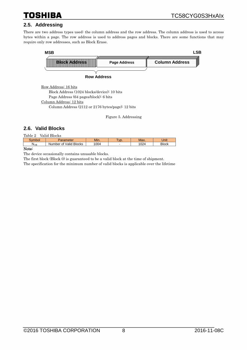
2.5. Addressing There are two address types used: the column address and the row address. The column address is used to access bytes within a page. The row address is used to address pages and blocks. There are some functions that may require only row addresses, such as Block Erase. Row Address Row Address: 16 bits Block Address (1024 blocks/device): 10 bits Page Address (64 pages/block): 6 bits Column Address: 12 bits Column Address (2112 or 2176 bytes/page): 12 bits
Figure 5. Addressing
2.6. Valid Blocks Table 2 Valid Blocks
Symbol Parameter Min. Typ. Max. Unit NVB Number of Valid Blocks 1004 - 1024 Block
Note: The device occasionally contains unusable blocks. The first block (Block 0) is guaranteed to be a valid block at the time of shipment. The specification for the minimum number of valid blocks is applicable over the lifetime
Block Address Page Address Column Address
MSB LSB

TC58CYG0S3HxAIx
©2016 TOSHIBA CORPORATION 2016-11-08C 9
3. Physical Interface
3.1. Absolute Maximum Rating Stresses greater than those listed in Table 3 may cause permanent damage to the device. This is a stress rating only. Table 3 Absolute Maximum Rating
Symbol Parameter Value Unit
VCC Power Supply Voltage −0.3 to 3.9 V
VIN Input Voltage −0.3 to VCC + 0.3 (≤ 3.9 V) V
VI/O Input /Output Voltage −0.3 to VCC + 0.3 (≤ 3.9 V) V
PD1 Power Dissipation 1 0.42 W
PD2 Power Dissipation 2 (WSON8 ePAD without solder) 0.27 W
TSOLDER Soldering Temperature (10 s) 260 °C
TSTG Storage Temperature −55 to 150 °C
TOPR Operating Temperature -40 to 85 °C
3.2. Capacitance Table 4 Capacitance (TOPR = 25℃, f = 1MHz) Symbol Parameter Condition Min. Max. Unit
CIN Input VIN = 0 V - 2.5 pF
COUT Output VOUT = 0 V - 4 pF
Note: This parameter is periodically sampled and is not tested for every device.
3.3. Recommended DC Operating Conditions Table 5 Recommended DC Operating Condition
Symbol Parameter Min. Typ. Max. Unit
VCC Power Supply Voltage 1.7 - 1.95 V
VIH High Level input Voltage VCC × 0.8 - VCC + 0.3 V
VIL Low Level Input Voltage -0.3 - VCC × 0.2 V
TC58CYG0S3HxAIx
©2016 TOSHIBA CORPORATION 2016-11-08C 10
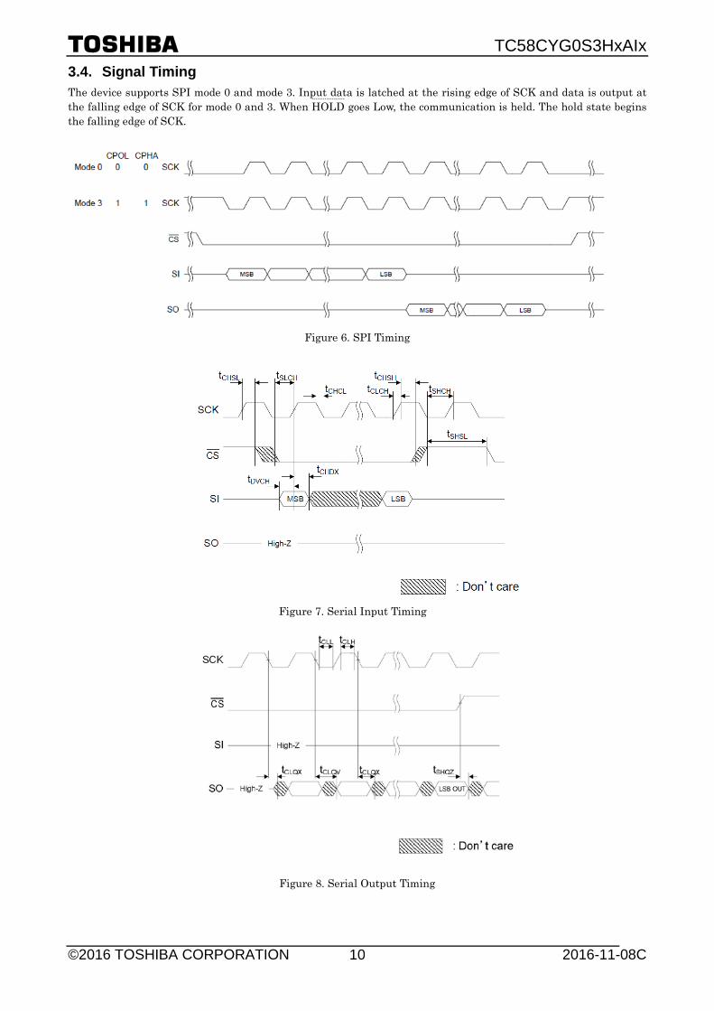
3.4. Signal Timing The device supports SPI mode 0 and mode 3. Input data is latched at the rising edge of SCK and data is output at the falling edge of SCK for mode 0 and 3. When HOLD
------------------ goes Low, the communication is held. The hold state begins
the falling edge of SCK.
Figure 6. SPI Timing
Figure 7. Serial Input Timing
Figure 8. Serial Output Timing
TC58CYG0S3HxAIx
©2016 TOSHIBA CORPORATION 2016-11-08C 11
Figure 9. Hold Timing
Figure 10. WP Timing (Example)
TC58CYG0S3HxAIx
©2016 TOSHIBA CORPORATION 2016-11-08C 12
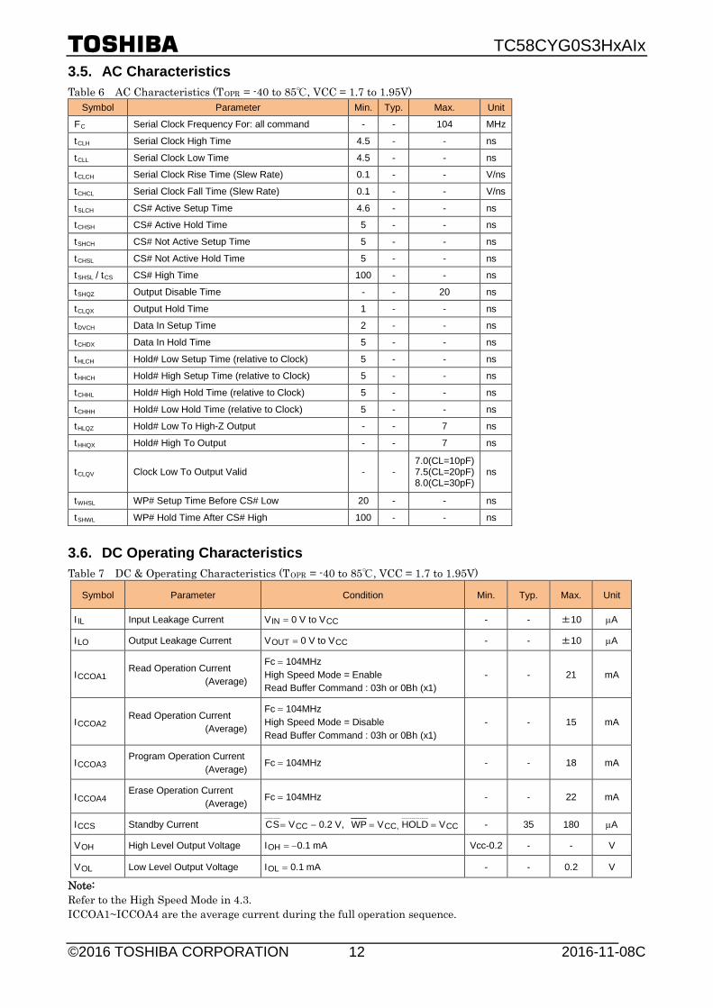
3.5. AC Characteristics Table 6 AC Characteristics (TOPR = -40 to 85℃, VCC = 1.7 to 1.95V)
Symbol Parameter Min. Typ. Max. Unit
FC Serial Clock Frequency For: all command - - 104 MHz
tCLH Serial Clock High Time 4.5 - - ns
tCLL Serial Clock Low Time 4.5 - - ns
tCLCH Serial Clock Rise Time (Slew Rate) 0.1 - - V/ns
tCHCL Serial Clock Fall Time (Slew Rate) 0.1 - - V/ns
tSLCH CS# Active Setup Time 4.6 - - ns
tCHSH CS# Active Hold Time 5 - - ns
tSHCH CS# Not Active Setup Time 5 - - ns
tCHSL CS# Not Active Hold Time 5 - - ns
tSHSL / tCS CS# High Time 100 - - ns
tSHQZ Output Disable Time - - 20 ns
tCLQX Output Hold Time 1 - - ns
tDVCH Data In Setup Time 2 - - ns
tCHDX Data In Hold Time 5 - - ns
tHLCH Hold# Low Setup Time (relative to Clock) 5 - - ns
tHHCH Hold# High Setup Time (relative to Clock) 5 - - ns
tCHHL Hold# High Hold Time (relative to Clock) 5 - - ns
tCHHH Hold# Low Hold Time (relative to Clock) 5 - - ns
tHLQZ Hold# Low To High-Z Output - - 7 ns
tHHQX Hold# High To Output - - 7 ns
tCLQV Clock Low To Output Valid - - 7.0(CL=10pF) 7.5(CL=20pF) 8.0(CL=30pF)
ns
tWHSL WP# Setup Time Before CS# Low 20 - - ns
tSHWL WP# Hold Time After CS# High 100 - - ns
3.6. DC Operating Characteristics Table 7 DC & Operating Characteristics (TOPR = -40 to 85℃, VCC = 1.7 to 1.95V)
Symbol Parameter Condition Min. Typ. Max. Unit
I IL Input Leakage Current VIN = 0 V to VCC - - ±10 µA
ILO Output Leakage Current VOUT = 0 V to VCC - - ±10 µA
ICCOA1 Read Operation Current
(Average)
Fc = 104MHz High Speed Mode = Enable Read Buffer Command : 03h or 0Bh (x1)
- - 21 mA
ICCOA2 Read Operation Current
(Average)
Fc = 104MHz High Speed Mode = Disable Read Buffer Command : 03h or 0Bh (x1)
- - 15 mA
ICCOA3 Program Operation Current
(Average) Fc = 104MHz - - 18 mA
ICCOA4 Erase Operation Current
(Average) Fc = 104MHz - - 22 mA
ICCS Standby Current CS----------
= VCC − 0.2 V, WP = VCC, EHOLDE
----------------
A = VCC - 35 180 µA
VOH High Level Output Voltage IOH = −0.1 mA Vcc-0.2 - - V
VOL Low Level Output Voltage IOL = 0.1 mA - - 0.2 V
Note: Refer to the High Speed Mode in 4.3. ICCOA1~ICCOA4 are the average current during the full operation sequence.

TC58CYG0S3HxAIx
©2016 TOSHIBA CORPORATION 2016-11-08C 13
3.7. Programming, Reading and Erasing Characteristics Table 8 Programming, Reading and Erasing Characteristics (TOPR = -40 to 85℃, VCC = 1.7 to 1.95V)
Symbol Parameter Min. Typ. Max. Unit
tPROG Programming Time - 360 500 µs
N Number of Partial Program Cycles in the Same Page - - 4 time
tBERASE Block Erasing Time - 2.7 10 ms
tR Cell Array to the Buffer (with ECC) (High Speed Mode = Disable) - 70 155 µs
tRHSA4 Average Read Time for Sequential Read (High Speed Mode = Enable, Read Buffer x4) - 30 - µs
tRST
Device Reset Time (Read) - - 155 µs
Device Reset Time (Program) - - 500 µs
Device Reset Time (Erase) - - 10 ms
Note: Refer to the data pair of ECC calculation in 4.16 Internal ECC. Refer to the High Speed Mode in 4.3. tR is the average busy time for page read operation of 64pages continuously in a block. tRHSA4 is the average busy time for sequential page read operation with all data output in each page of 64pages continuously in a block. The busy time after Protect Execute command is shorter than tPROG (Max.).
3.8. Power ON/OFF Sequence The timing sequence shown in the figure below is necessary for the power ON/OFF sequence. The device internal initialization starts after the power supply reaches an appropriate level in the power on sequence. The users cannot issue any commands while tVSL. From the end of tVSL to the end of tVOP, Get Feature Operation and Reset Operation can be issued. OIP bit in the feature table indicates the busy state in this time period. All operations are available after tVOP.
Figure 11. Power ON/OFF Sequence Table 9 Power on Timing
Symbol Parameter Min. Max. Unit
tVSL VCC(min) to CS---------
Low - 100 µs
tVOP VCC(min) to all operation - 1.1 ms
tPUW Waiting time for power on 1 - ms
VCCSR VCC Slew Rate - 136 mV/µs
3.9. AC Test Condition Table 10 AC Test Condition
PARAMETER CONDITION
VCC: 1.7 to 1.95V Input level VCC × 0.2 to VCC × 0.8
Input pulse rise and fall time 2 ns
Input comparison level Vcc / 2
Output data comparison level Vcc / 2
Output load CL (30pF) + 1 TTL
0 V
VCC 1.7 V
Reset, Get Feature
tPUW
1.7 V
0.5 V 0.5 V tVSL
tVOP
All operations.
1.7 V
Available operation: Available operations:
TC58CYG0S3HxAIx
©2016 TOSHIBA CORPORATION 2016-11-08C 14
4. Command Description and Device Operation
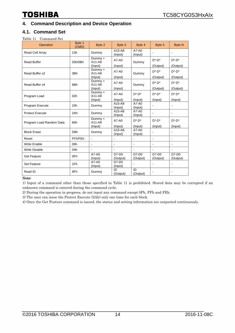
4.1. Command Set Table 11 Command Set
Operation Byte 1 Byte 2 Byte 3 Byte 4 Byte 5 Byte N (CMD)
Read Cell Array 13h Dummy A15-A8 A7-A0 - - (Input) (Input)
Read Buffer 03h/0Bh Dummy + A11-A8 A7-A0 Dummy D*-D* D*-D*
(Input) (Input) (Output) (Output)
Read Buffer x2 3Bh Dummy + A11-A8 A7-A0 Dummy D*-D* D*-D*
(Input) (Input) (Output) (Output)
Read Buffer x4 6Bh Dummy + A11-A8 A7-A0 Dummy D*-D* D*-D*
(Input) (Input) (Output) (Output)
Program Load 02h Dummy + A11-A8 A7-A0 D*-D* D*-D* D*-D*
(Input) (Input) (Input) (Input) (Input)
Program Execute 10h Dummy A15-A8 A7-A0 - - (Input) (Input)
Protect Execute 2Ah Dummy A15-A8 A7-A0 - - (Input) (Input)
Program Load Random Data 84h Dummy + A11-A8 A7-A0 D*-D* D*-D* D*-D*
(Input) (Input) (Input) (Input) (Input)
Block Erase D8h Dummy A15-A8 A7-A0 - - (Input) (Input) Reset FFh/FEh - - - - -
Write Enable 06h - - - - -
Write Disable 04h - - - - -
Get Feature 0Fh A7-A0 D7-D0 D7-D0 D7-D0 D7-D0 (Input) (Output) (Output) (Output) (Output)
Set Feature 1Fh A7-A0 D7-D0 - - - (Input) (Input)
Read ID 9Fh Dummy ID ID - - (Output) (Output) Note: 1) Input of a command other than those specified in Table 11 is prohibited. Stored data may be corrupted if an unknown command is entered during the command cycle. 2) During the operation in progress, do not input any command except 0Fh, FFh and FEh. 3) The user can issue the Protect Execute (2Ah) only one time for each block. 4) Once the Get Feature command is issued, the status and setting information are outputted continuously.
TC58CYG0S3HxAIx
©2016 TOSHIBA CORPORATION 2016-11-08C 15
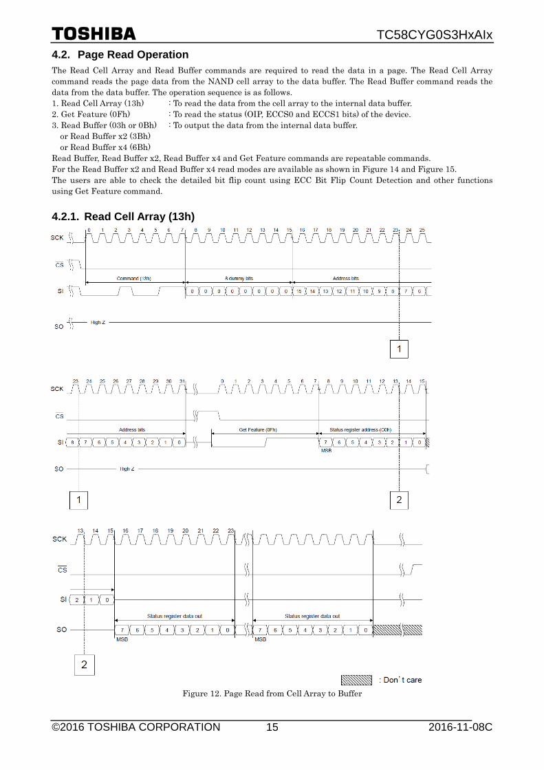
4.2. Page Read Operation The Read Cell Array and Read Buffer commands are required to read the data in a page. The Read Cell Array command reads the page data from the NAND cell array to the data buffer. The Read Buffer command reads the data from the data buffer. The operation sequence is as follows. 1. Read Cell Array (13h) : To read the data from the cell array to the internal data buffer. 2. Get Feature (0Fh) : To read the status (OIP, ECCS0 and ECCS1 bits) of the device. 3. Read Buffer (03h or 0Bh) : To output the data from the internal data buffer. or Read Buffer x2 (3Bh) or Read Buffer x4 (6Bh) Read Buffer, Read Buffer x2, Read Buffer x4 and Get Feature commands are repeatable commands. For the Read Buffer x2 and Read Buffer x4 read modes are available as shown in Figure 14 and Figure 15. The users are able to check the detailed bit flip count using ECC Bit Flip Count Detection and other functions using Get Feature command.
4.2.1. Read Cell Array (13h)
Figure 12. Page Read from Cell Array to Buffer

TC58CYG0S3HxAIx
©2016 TOSHIBA CORPORATION 2016-11-08C 16
4.2.2. Read Buffer (03h or 0Bh) Note: When internal ECC is turned OFF, the maximum output data size is 2176 Bytes.
Figure 13. Page Read from Buffer Timing
TC58CYG0S3HxAIx
©2016 TOSHIBA CORPORATION 2016-11-08C 17
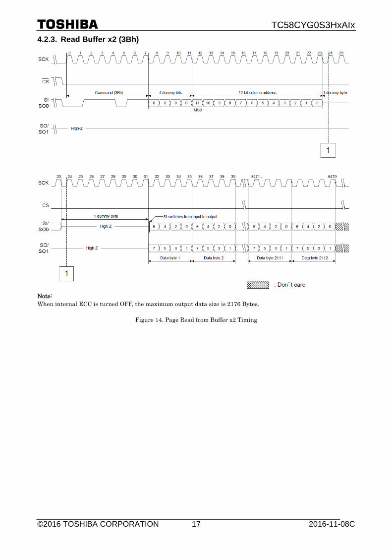
4.2.3. Read Buffer x2 (3Bh) Note: When internal ECC is turned OFF, the maximum output data size is 2176 Bytes.
Figure 14. Page Read from Buffer x2 Timing
TC58CYG0S3HxAIx
©2016 TOSHIBA CORPORATION 2016-11-08C 18
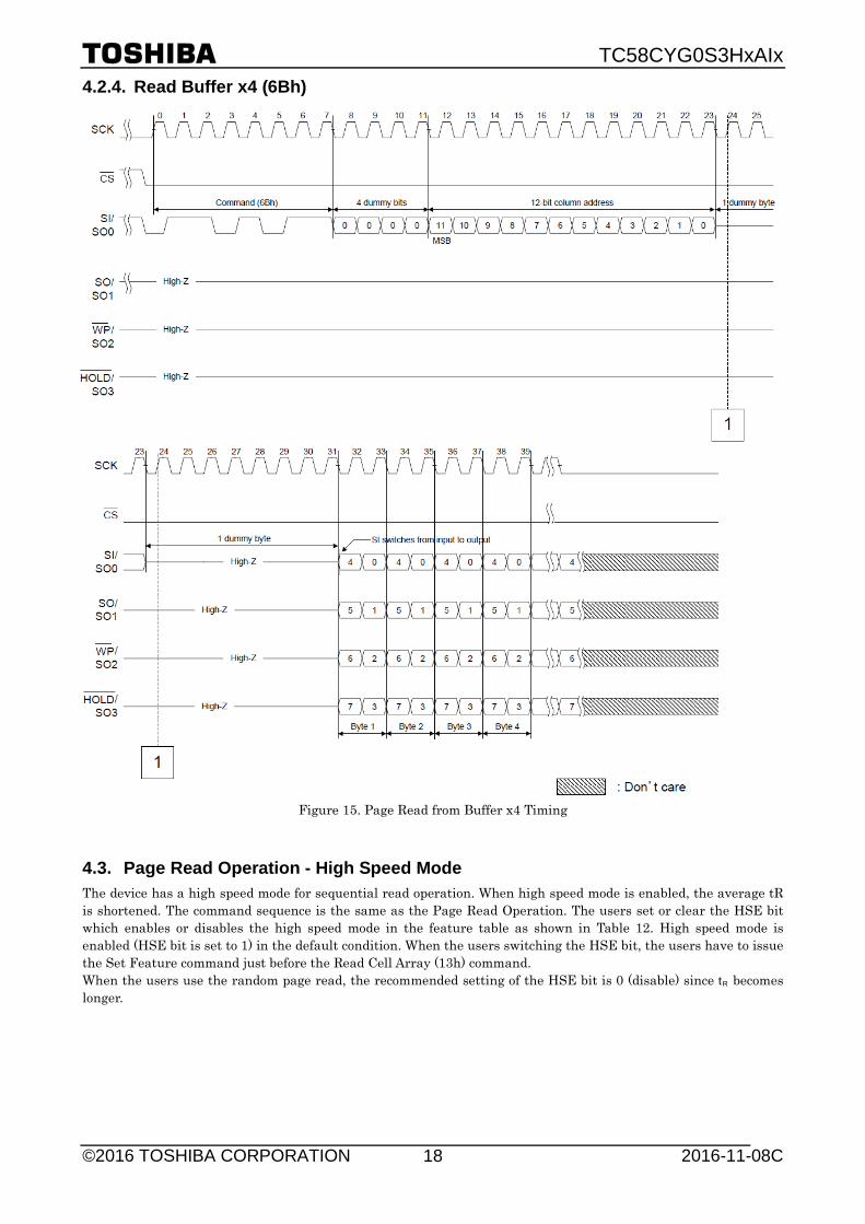
4.2.4. Read Buffer x4 (6Bh)
Figure 15. Page Read from Buffer x4 Timing
4.3. Page Read Operation - High Speed Mode The device has a high speed mode for sequential read operation. When high speed mode is enabled, the average tR is shortened. The command sequence is the same as the Page Read Operation. The users set or clear the HSE bit which enables or disables the high speed mode in the feature table as shown in Table 12. High speed mode is enabled (HSE bit is set to 1) in the default condition. When the users switching the HSE bit, the users have to issue the Set Feature command just before the Read Cell Array (13h) command. When the users use the random page read, the recommended setting of the HSE bit is 0 (disable) since tR becomes longer.
TC58CYG0S3HxAIx
©2016 TOSHIBA CORPORATION 2016-11-08C 19
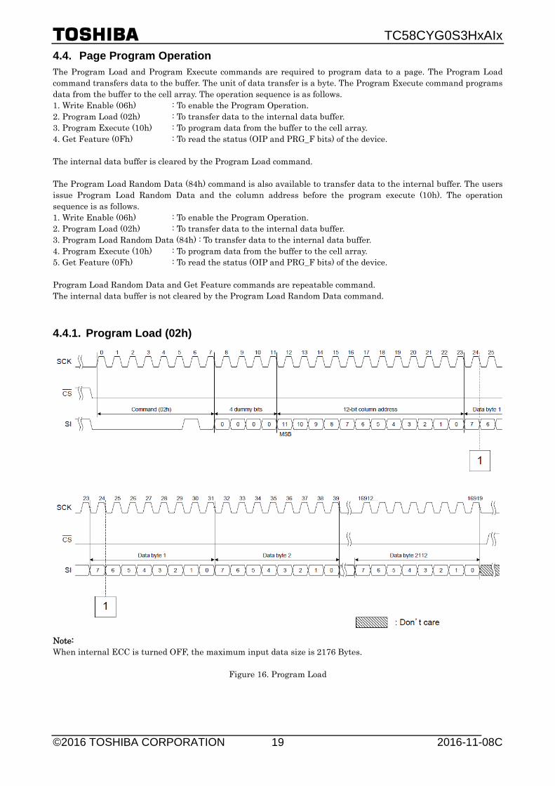
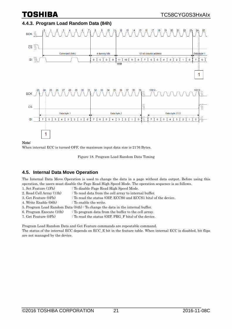
4.4. Page Program Operation The Program Load and Program Execute commands are required to program data to a page. The Program Load command transfers data to the buffer. The unit of data transfer is a byte. The Program Execute command programs data from the buffer to the cell array. The operation sequence is as follows. 1. Write Enable (06h) : To enable the Program Operation. 2. Program Load (02h) : To transfer data to the internal data buffer. 3. Program Execute (10h) : To program data from the buffer to the cell array. 4. Get Feature (0Fh) : To read the status (OIP and PRG_F bits) of the device. The internal data buffer is cleared by the Program Load command. The Program Load Random Data (84h) command is also available to transfer data to the internal buffer. The users issue Program Load Random Data and the column address before the program execute (10h). The operation sequence is as follows. 1. Write Enable (06h) : To enable the Program Operation. 2. Program Load (02h) : To transfer data to the internal data buffer. 3. Program Load Random Data (84h) : To transfer data to the internal data buffer. 4. Program Execute (10h) : To program data from the buffer to the cell array. 5. Get Feature (0Fh) : To read the status (OIP and PRG_F bits) of the device. Program Load Random Data and Get Feature commands are repeatable command. The internal data buffer is not cleared by the Program Load Random Data command.
4.4.1. Program Load (02h) Note: When internal ECC is turned OFF, the maximum input data size is 2176 Bytes.
Figure 16. Program Load
TC58CYG0S3HxAIx
©2016 TOSHIBA CORPORATION 2016-11-08C 20
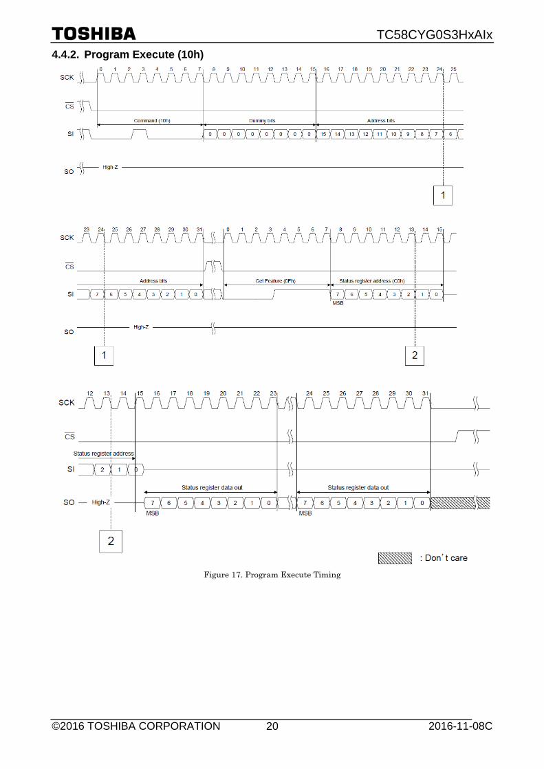
4.4.2. Program Execute (10h)
Figure 17. Program Execute Timing
TC58CYG0S3HxAIx
©2016 TOSHIBA CORPORATION 2016-11-08C 21
4.4.3. Program Load Random Data (84h) Note: When internal ECC is turned OFF, the maximum input data size is 2176 Bytes.
Figure 18. Program Load Random Data Timing
4.5. Internal Data Move Operation The Internal Data Move Operation is used to change the data in a page without data output. Before using this operation, the users must disable the Page Read High Speed Mode. The operation sequence is as follows. 1. Set Feature (1Fh) : To disable Page Read High Speed Mode. 2. Read Cell Array (13h) : To read data from the cell array to internal buffer. 3. Get Feature (0Fh) : To read the status (OIP, ECCS0 and ECCS1 bits) of the device. 4. Write Enable (06h) : To enable the write. 5. Program Load Random Data (84h) : To change the data in the internal buffer. 6. Program Execute (10h) : To program data from the buffer to the cell array. 7. Get Feature (0Fh) : To read the status (OIP, PRG_F bits) of the device. Program Load Random Data and Get Feature commands are repeatable command. The status of the internal ECC depends on ECC_E bit in the feature table. When internal ECC is disabled, bit flips are not managed by the device.
TC58CYG0S3HxAIx
©2016 TOSHIBA CORPORATION 2016-11-08C 22
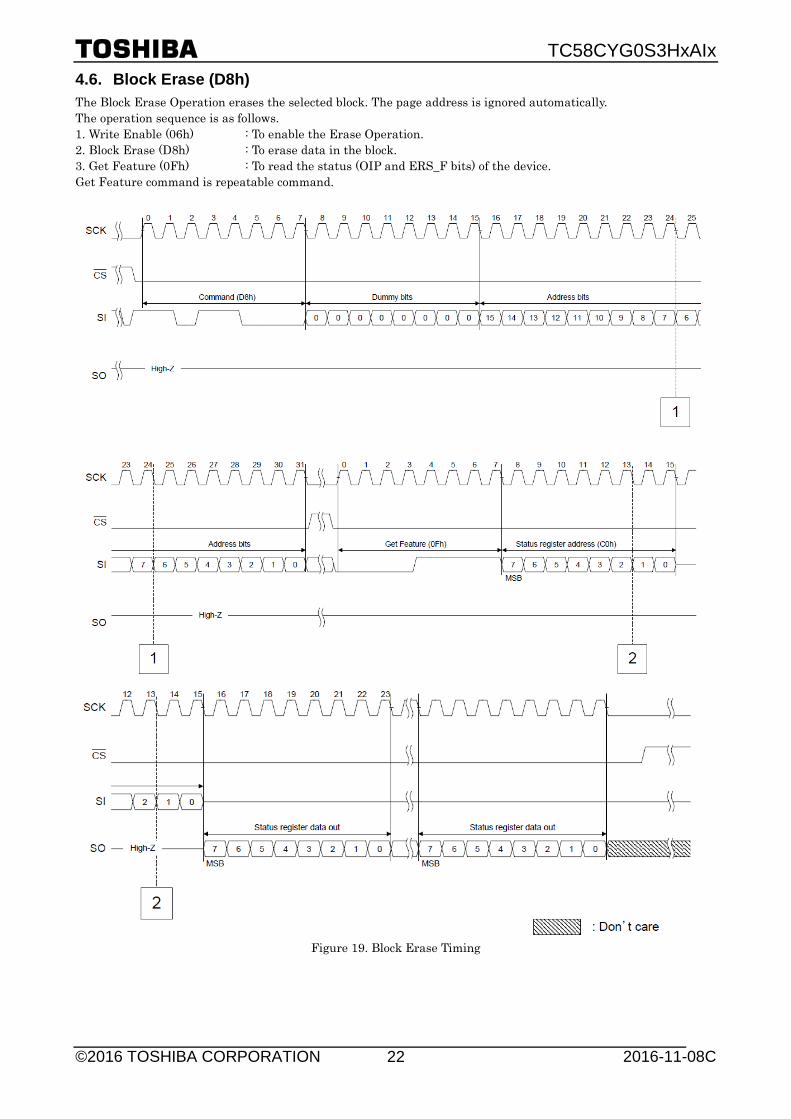
4.6. Block Erase (D8h) The Block Erase Operation erases the selected block. The page address is ignored automatically. The operation sequence is as follows. 1. Write Enable (06h) : To enable the Erase Operation. 2. Block Erase (D8h) : To erase data in the block. 3. Get Feature (0Fh) : To read the status (OIP and ERS_F bits) of the device. Get Feature command is repeatable command.
Figure 19. Block Erase Timing
TC58CYG0S3HxAIx
©2016 TOSHIBA CORPORATION 2016-11-08C 23
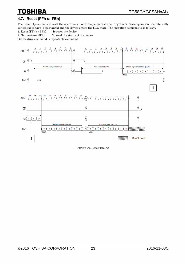
4.7. Reset (FFh or FEh) The Reset Operation is to reset the operations. For example, in case of a Program or Erase operation, the internally generated voltage is discharged and the device enters the busy state. The operation sequence is as follows. 1. Reset (FFh or FEh) :To reset the device 2. Get Feature (0Fh) :To read the status of the device Get Feature command is repeatable command.
Figure 20. Reset Timing

TC58CYG0S3HxAIx
©2016 TOSHIBA CORPORATION 2016-11-08C 24
4.8. Write Enable (06h) / Write Disable (04h) The Write Enable / Disable commands set or reset the WEL (-Write Enable Latch) bit in the feature table shown in Table 12. The Write Enable command sets the WEL bit to 1. The Write Enable command must be issued before the Page Program, Block Protection and Block Erase operations. The Write Disable command clears the WEL bit to 0. If the WEL bit is cleared, Page Program, Block Protection and Block Erase commands are ignored by the device.
Figure 21. Write Enable
Figure 22. Write Disable Timing
TC58CYG0S3HxAIx
©2016 TOSHIBA CORPORATION 2016-11-08C 25
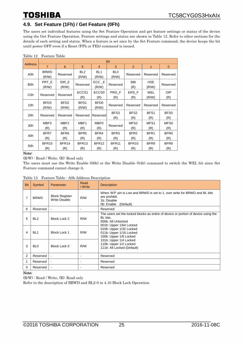
4.9. Set Feature (1Fh) / Get Feature (0Fh) The users set individual features using the Set Feature Operation and get feature settings or status of the device using the Get Feature Operation. Feature settings and status are shown in Table 12. Refer to other sections for the details of each setting and status. When a feature is set once by the Set Feature command, the device keeps the bit until power OFF even if a Reset (FFh or FEh) command is issued. Table 12 Feature Table
Address Bit
7 6 5 4 3 2 1 0
A0h BRWD (R/W)
Reserved BL2
(R/W) BL1
(R/W) BL0
(R/W) Reserved Reserved Reserved
B0h PRT_E (R/W)
IDR_E (R/W)
Reserved ECC _E (R/W)
Reserved BBI (R)
HSE (R/W)
Reserved
C0h Reserved Reserved ECCS1
(R) ECCS0
(R) PRG_F
(R) ERS_F
(R) WEL (R/W)
OIP (R)
10h BFD3 (R/W)
BFD2 (R/W)
BFD1 (R/W)
BFD0 (R/W)
Reserved Reserved Reserved Reserved
20h Reserved Reserved Reserved Reserved BFS3 (R)
BFS2 (R)
BFS1 (R)
BFS0 (R)
30h MBF3
(R) MBF2
(R) MBF1
(R) MBF0
(R) Reserved
MFS2 (R)
MFS1 (R)
MFS0 (R)
40h BFR7
(R) BFR6
(R) BFR5
(R) BFR4
(R) BFR3
(R) BFR2
(R) BFR1
(R) BFR0
(R)
50h BFR15
(R) BFR14
(R) BFR13
(R) BFR12
(R) BFR11
(R) BFR10
(R) BFR9
(R) BFR8
(R) Note: (R/W) : Read / Write, (R): Read only The users must use the Write Enable (06h) or the Write Disable (04h) command to switch the WEL bit since Set Feature command cannot change it. Table 13 Feature Table - A0h Address Description
Bit Symbol Parameter Read / Write Description
7 BRWD Block Register Write Disable R/W
When WP------------
pin is Low and BRWD is set to 1, over write for BRWD and BL bits are prohibit. 1b: Disable 0b: Enable (Default)
6 Reserved - - Reserved
5 BL2 Block Lock 2 R/W The users set the locked blocks as entire of device or portion of device using the BL bits. 000b: All Unlocked 001b: Upper 1/64 Locked 010b: Upper 1/32 Locked 011b: Upper 1/16 Locked 100b: Upper 1/8 Locked 101b: Upper 1/4 Locked 110b: Upper 1/2 Locked 111b: All Locked (Default)
4 BL1 Block Lock 1 R/W
3 BL0 Block Lock 0 R/W
2 Reserved - - Reserved
1 Reserved - - Reserved
0 Reserved - - Reserved
Note: (R/W) : Read / Write, (R): Read only Refer to the description of BRWD and BL2-0 in 4.10 Block Lock Operation.

TC58CYG0S3HxAIx
©2016 TOSHIBA CORPORATION 2016-11-08C 26
Table 14 Feature Table - B0h Address Description
Bit Symbol Parameter Read / Write Description
7 PRT_E Block Protect Enable R/W
The setting for Block Protection. 0b: Normal Operation (Default) 1b: Block Protection Enable – The protect execute command (2Ah) is acceptable for block protection.
6 IDR _E ID Read Enable R/W The setting for Parameter Page Read and Unique ID Read. 0b: Normal Operation (Default) 1b: Parameter Page Read and Unique ID read mode
5 Reserved - - Reserved
4 ECC _E ECC Enable R/W The setting for internal ECC Function. 0b: Internal ECC Disable 1b: Internal ECC Enable (Default)
3 Reserved - - Reserved
2 BBI Bad Block Inhibit R The setting for Bad Block Inhibit Function. 0b: Not Available 1b: Bad Block Inhibit Enable (Default)
1 HSE High Speed Mode Enable R/W The setting for Page Read High Speed Mode. 0b: High Speed Mode Disable 1b: High Speed Mode Enable (Default)
0 Reserved - - Reserved Note: (R/W) : Read / Write, (R): Read only Refer to the description of PRT_E in 4.11 Block Protection Operation (One Time Program) Refer to the description of ECC_E in 4.16.1 ECC Switch. Refer to the description of BBI in 4.15 Bad Block Inhibit. Refer to the description of HSE in 4.3 Page Read Operation - High Speed Mode. Table 15 Feature Table - C0h Address Description Bit Symbol Parameter Read
/ Write Description
7 Reserved - - Reserved 6 Reserved - - Reserved
5 ECCS1 ECC Status 1 R
ECC status bits indicate the status of internal ECC operation. 00b: No bit flips were detected in previous page read. 01b: Bit flips were detected and corrected. Bit flip count did not exceed the bit flip detection threshold. The threshold is set by bits [7:4] in address 10h in the feature table. 10b: Multiple bit flips were detected and not corrected. 11b: Bit flips were detected and corrected. Bit flip count exceeded the bit flip detection threshold. The threshold is set by bits [7:4] in address 10h in the feature table.
4 ECCS0 ECC Status 0 R
3 PRG_F Program Fail R
Program fail bit indicates that a program failure has occurred in the previous Program Operation. 0b: Program Pass 1b: Program Fail
2 ERS_F Erase Fail R
Erase fail bit indicates that an erase failure has occurred in the previous Erase Operation. 0b: Erase Pass 1b: Erase Fail
1 WEL Write Enable Latch R/W This bit indicates the status of write enable/disable. 0b: Write Disable (Default) 1b: Write Enable
0 OIP Operation In Progress R
This bit indicates the status of the device. This bit will be set while busy state. 0b: Operation is not in progress. Ready state. 1b: Operation is in progress. Busy state.
Note: (R/W) : Read / Write, (R): Read only The users must use the Write Enable (06h) or the Write Disable (04h) command to switch the WEL bit since Set Feature command cannot change it. Once the Get Feature command is issued, the status and setting information are outputted continuously. OIP bit is updated automatically during the status information are outputted continuously.

TC58CYG0S3HxAIx
©2016 TOSHIBA CORPORATION 2016-11-08C 27
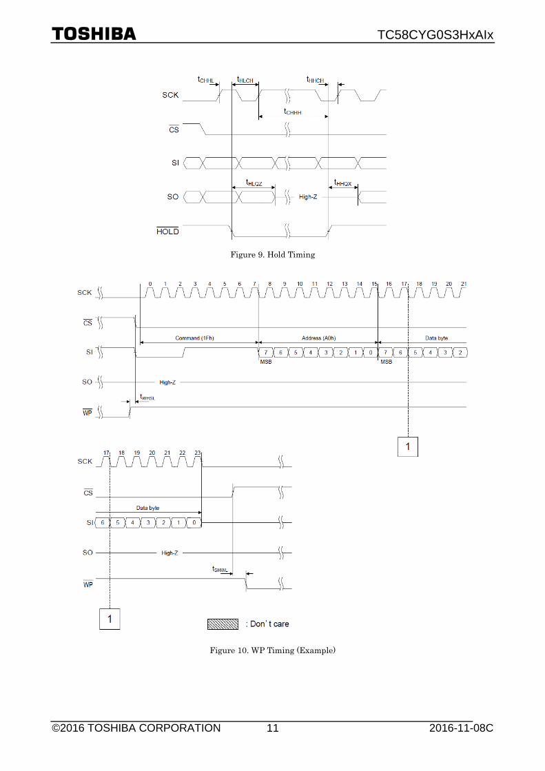
4.9.1. Set Feature (1Fh)
Figure 23. Set Feature Timing
4.9.2. Get Feature (0Fh) After the Get Feature command and the address are inputted, the 8bit status and setting information will be outputted continuously until CS
----------
goes High.
Figure 24. Get Feature Timing
TC58CYG0S3HxAIx
©2016 TOSHIBA CORPORATION 2016-11-08C 28
4.10. Block Lock Operation The Block Lock Operation locks blocks and prevents Program and Erase operations. The users set the range of locked blocks as the entire device or a portion of the device using the BL bits (bits [5:3]) in address A0h of the feature table shown in Table 12. The users set the BL bits by the Set Feature Operation. After the power on sequence, all blocks are locked (bits [5:3] are all set to 1). If the Program Execute (10h) or Block Erase (D8h) command is issued to locked blocks, Program Fail or Erase Fail will be indicated in the feature table shown in Table 12. The users must clear / change the BL bits using Set Feature command to unlock the entire of the device or portion of the device. When BRWD bit is set and WP
-------------
pin is Low, the users cannot switch the BRWD and the BL bits. The Block Lock Operation is different from the Block Protection Operation. Table 16 Block Lock Setting BL2 BL1 BL0 Protect Area
0 0 0 All Unlocked
0 0 1 Upper 1/64 Locked
0 1 0 Upper 1/32 Locked
0 1 1 Upper 1/16 Locked
1 0 0 Upper 1/8 Locked
1 0 1 Upper 1/4 Locked
1 1 0 Upper 1/2 Locked
1 1 1 All Locked
4.11. Block Protection Operation (One Time Program) The Block Protection Operation provides the function to prohibit the Program and Erase operations to user selected blocks. The users protect individual blocks using the Set Feature, Write Enable and Protect Execute commands. The last 128 blocks of the device are able to be set to protected blocks. The block protection setting is permanent. Once a block is protected, the user cannot unprotect the block. When PRT_E (bit [7]) in address B0h of the feature table is set to 1, and the users issue the Protect Execute command (2Ah), the user block will become a protected block. The users must set the PRT_E bit (bit [7]) just before the Write Enable command for the Protect Execute. After the protection to the block, the users must clear bit [7] in address B0h using the Set Feature command. The users can issue the Protect Execute (2Ah) only one time for each block. The Block Protection Operation is different from the Block Lock Operation. The operation sequence to set block “N” as a protected block is as follows. 1. Set Feature (1Fh) : To set PRT_E bit [7] in address B0h to block protection mode. 2. Write Enable (06h) : To enable the protect execute command. 3. Protect Execute (2Ah) for block “N” : To protect the block “N”. 4. Get Feature (0Fh) : To read the status (OIP and PRG_F bits) of the device. 5. Set Feature (1Fh) : To clear PRT_E bit [7] in address B0h. Table 17 Block Protection Setting PRT_E State
0 Normal Operation (Default)
1 Block Protection Enable – The Protect Execute command (2Ah) is acceptable for block protection.
Table 18 Block Number for Block Protection
Block Number Block Protection Block 0 – Block 895 The users cannot protect these blocks by block protection operation. Block 896 – Block1023 The users can protect these blocks by block protection operation.

TC58CYG0S3HxAIx
©2016 TOSHIBA CORPORATION 2016-11-08C 29
4.11.1. Protect Execute (2Ah)
Figure 25. Protect Execute Timing
TC58CYG0S3HxAIx
©2016 TOSHIBA CORPORATION 2016-11-08C 30
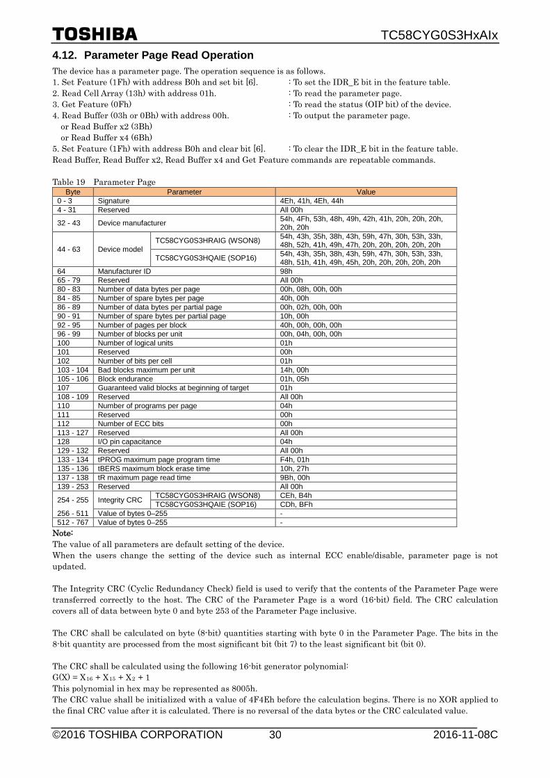
4.12. Parameter Page Read Operation The device has a parameter page. The operation sequence is as follows. 1. Set Feature (1Fh) with address B0h and set bit [6]. : To set the IDR_E bit in the feature table. 2. Read Cell Array (13h) with address 01h. : To read the parameter page. 3. Get Feature (0Fh) : To read the status (OIP bit) of the device. 4. Read Buffer (03h or 0Bh) with address 00h. : To output the parameter page. or Read Buffer x2 (3Bh) or Read Buffer x4 (6Bh) 5. Set Feature (1Fh) with address B0h and clear bit [6]. : To clear the IDR_E bit in the feature table. Read Buffer, Read Buffer x2, Read Buffer x4 and Get Feature commands are repeatable commands. Table 19 Parameter Page
Byte Parameter Value 0 - 3 Signature 4Eh, 41h, 4Eh, 44h 4 - 31 Reserved All 00h
32 - 43 Device manufacturer 54h, 4Fh, 53h, 48h, 49h, 42h, 41h, 20h, 20h, 20h, 20h, 20h
44 - 63 Device model TC58CYG0S3HRAIG (WSON8) 54h, 43h, 35h, 38h, 43h, 59h, 47h, 30h, 53h, 33h,
48h, 52h, 41h, 49h, 47h, 20h, 20h, 20h, 20h, 20h
TC58CYG0S3HQAIE (SOP16) 54h, 43h, 35h, 38h, 43h, 59h, 47h, 30h, 53h, 33h, 48h, 51h, 41h, 49h, 45h, 20h, 20h, 20h, 20h, 20h
64 Manufacturer ID 98h 65 - 79 Reserved All 00h 80 - 83 Number of data bytes per page 00h, 08h, 00h, 00h 84 - 85 Number of spare bytes per page 40h, 00h 86 - 89 Number of data bytes per partial page 00h, 02h, 00h, 00h 90 - 91 Number of spare bytes per partial page 10h, 00h 92 - 95 Number of pages per block 40h, 00h, 00h, 00h 96 - 99 Number of blocks per unit 00h, 04h, 00h, 00h 100 Number of logical units 01h 101 Reserved 00h 102 Number of bits per cell 01h 103 - 104 Bad blocks maximum per unit 14h, 00h 105 - 106 Block endurance 01h, 05h 107 Guaranteed valid blocks at beginning of target 01h 108 - 109 Reserved All 00h 110 Number of programs per page 04h 111 Reserved 00h 112 Number of ECC bits 00h 113 - 127 Reserved All 00h 128 I/O pin capacitance 04h 129 - 132 Reserved All 00h 133 - 134 tPROG maximum page program time F4h, 01h 135 - 136 tBERS maximum block erase time 10h, 27h 137 - 138 tR maximum page read time 9Bh, 00h 139 - 253 Reserved All 00h
254 - 255 Integrity CRC TC58CYG0S3HRAIG (WSON8) CEh, B4h TC58CYG0S3HQAIE (SOP16) CDh, BFh
256 - 511 Value of bytes 0–255 - 512 - 767 Value of bytes 0–255 -
Note: The value of all parameters are default setting of the device. When the users change the setting of the device such as internal ECC enable/disable, parameter page is not updated. The Integrity CRC (Cyclic Redundancy Check) field is used to verify that the contents of the Parameter Page were transferred correctly to the host. The CRC of the Parameter Page is a word (16-bit) field. The CRC calculation covers all of data between byte 0 and byte 253 of the Parameter Page inclusive. The CRC shall be calculated on byte (8-bit) quantities starting with byte 0 in the Parameter Page. The bits in the 8-bit quantity are processed from the most significant bit (bit 7) to the least significant bit (bit 0). The CRC shall be calculated using the following 16-bit generator polynomial: G(X) = X16 + X15 + X2 + 1 This polynomial in hex may be represented as 8005h. The CRC value shall be initialized with a value of 4F4Eh before the calculation begins. There is no XOR applied to the final CRC value after it is calculated. There is no reversal of the data bytes or the CRC calculated value.

TC58CYG0S3HxAIx
©2016 TOSHIBA CORPORATION 2016-11-08C 31
4.13. Read ID (9Fh) The ID of the device is read by command 9Fh. Table 20 ID Table
Byte Description Value
Byte 0 Manufacture ID (Toshiba) 98h
Byte 1 Device ID B2h
Figure 26. Read ID Timing
4.14. Unique ID Read Operation The device has a unique ID and it is different for each device. The device has 16 copies of 32 bytes of unique ID data. The first 16 bytes of data are unique ID data and the second 16 bytes of data are the complement value of the first 16 bytes of data. The operation sequence is as follows. 1. Set Feature (1Fh) with address B0h and set bit [6]. : To set the IDR_E bit in the feature table. 2. Read Cell Array (13h) with address 00h. : To read the unique ID. 3. Get Feature (0Fh) : To read the status (OIP bit) of the device. 4. Read Buffer (03h or 0Bh) with address 00h. : To output the 16 copies of the Unique ID. or Read Buffer x2 (3Bh) or Read Buffer x4 (6Bh) 5. Set Feature (1Fh) with address B0h and clear bit [6]. : To clear the IDR_E bit in the feature table. Read Buffer, Read Buffer x2, Read Buffer x4 and Get Feature commands are repeatable commands.
4.15. Bad Block Inhibit The device occasionally contains unusable blocks in its initial condition. The page program operation and erase operation are prohibited to invalid blocks. The device has a bad block inhibit function to protect initial invalid blocks. When the users issue the program or erase command to the initial invalid blocks, the device ignores these commands automatically and program fail or erase fail is indicated in the feature table as shown in Table 12. The bad block inhibit function is enabled by default and this setting is permanent.
TC58CYG0S3HxAIx
©2016 TOSHIBA CORPORATION 2016-11-08C 32
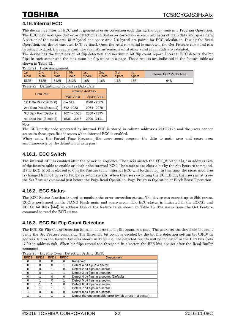
4.16. Internal ECC The device has internal ECC and it generates error correction code during the busy time in a Program Operation. The ECC logic manages 9bit error detection and 8bit error correction in each 528 bytes of main data and spare data. A section of the main area (512 bytes) and spare area (16 bytes) are paired for ECC calculation. During the Read Operation, the device executes ECC by itself. Once the read command is executed, the Get Feature command can be issued to check the read status. The read status remains until other valid commands are executed. The device has the functions of bit flip detection and maximum bit flip count report. Internal ECC detects the bit flips in each sector and the maximum bit flip count in a page. These results are indicated in the feature table as shown in Table 12. Table 21 Page Assignment 1st Main
2nd Main
3rd Main
4th Main
1st Spare
2nd Spare
3rd Spare
4th Spare Internal ECC Parity Area
512B 512B 512B 512B 16B 16B 16B 16B 64B
Table 22 Definition of 528 bytes Data Pair
Data Pair Column Address
Main Area Spare Area
1st Data Pair (Sector 0) 0 – 511 2048 - 2063
2nd Data Pair (Sector 1) 512- 1023 2064 - 2079
3rd Data Pair (Sector 2) 1024 – 1535 2080 - 2095
4th Data Pair (Sector 3) 1536 – 2047 2096 - 2111
Note: The ECC parity code generated by internal ECC is stored in column addresses 2112-2175 and the users cannot access to these specific addresses when internal ECC is enabled. While using the Partial Page Program, the users must program the data to main area and spare area simultaneously by the definition of data pair.
4.16.1. ECC Switch The internal ECC is enabled after the power on sequence. The users switch the ECC_E bit (bit [4]) in address B0h of the feature table to enable or disable the internal ECC. The users set or clear a bit by the Set Feature command. If the ECC_E bit is cleared to 0 in the feature table, internal ECC will be disabled. In this case, the spare area size is changed from 64 bytes to 128 bytes automatically. When the users switching the ECC_E bit, the users must issue the Set Feature command just before the Page Read Operation, Page Program Operation or Block Erase Operation.
4.16.2. ECC Status The ECC Status function is used to monitor the error correction status. The device can correct up to 8bit errors. ECC is performed on the NAND Flash main and spare areas. The ECC status is indicated in the ECCS1 and ECCS0 bit (bits [5:4]) in address C0h of the feature table shown in Table 15. The users issue the Get Feature command to read the ECC status.
4.16.3. ECC Bit Flip Count Detection The ECC Bit Flip Count Detection function detects the bit flip count in a page. The users set the threshold bit count using the Set Feature command. The threshold bit count is decided by the bit flip detection setting bit (BFD) in address 10h in the feature table as shown in Table 12. The detected results will be indicated in the BFS bits (bits [7:0]) in address 20h. When bit flips exceed the threshold in a sector, the BFS bits are set after the Read Buffer command. Table 23 Bit Flip Count Detection Setting (BFD) BFD3 BFD2 BFD1 BFD0 Description
0 0 0 0 Reserved 0 0 0 1 Detect a bit flip in a sector. 0 0 1 0 Detect 2 bit flips in a sector. 0 0 1 1 Detect 3 bit flips in a sector. 0 1 0 0 Detect 4 bit flips in a sector. (Default) 0 1 0 1 Detect 5 bit flips in a sector. 0 1 1 0 Detect 6 bit flips in a sector. 0 1 1 1 Detect 7 bit flips in a sector. 1 0 0 0 Detect 8 bit flips in a sector. 1 1 1 1 Detect the uncorrectable error (9+ bit errors in a sector).

TC58CYG0S3HxAIx
©2016 TOSHIBA CORPORATION 2016-11-08C 33
Table 24 Bit Flip Count Detection Status (BFS) (Feature Table - 20h Address Description)
Bit Symbol Parameter Read / Write Description
7 Reserved - - Reserved
6 Reserved - - Reserved
5 Reserved - - Reserved
4 Reserved - - Reserved
3 BFS3 Bit Flip Count Detection Status 3 R
Bit flip count detection status 3 indicates that the bit flip count in sector 3 is more than threshold bit count. 0b: Bit flip count in sector 3 is less than the threshold. 1b: Bit flip count in sector 3 is the threshold bit count or more than the threshold bit count.
2 BFS2 Bit Flip Count Detection Status 2 R
Bit flip count detection status 2 indicates that the bit flip count in sector 2 is more than threshold bit count. 0b: Bit flip count in sector 2 is less than the threshold. 1b: Bit flip count in sector 2 is the threshold bit count or more than the threshold bit count.
1 BFS1 Bit Flip Count Detection Status 1 R
Bit flip count detection status 1 indicates that the bit flip count in sector 1 is more than threshold bit count. 0b: Bit flip count in sector 1 is less than the threshold. 1b: Bit flip count in sector 1 is the threshold bit count or more than the threshold bit count.
0 BFS0 Bit Flip Count Detection Status 0 R
Bit flip count detection status 0 indicates that the bit flip count in sector 0 is more than threshold bit count. 0b: Bit flip count in sector 0 is less than the threshold. 1b: Bit flip count in sector 0 is the threshold bit count or more than the threshold bit count.
4.16.4. ECC Bit Flip Count Report The ECC Bit Flip Count Report function reports the bit flip count of each sector in a page. The users can read the bit flip count using the Get Feature command with address 40h and 50h. Table 25 Bit Flip Count Report for Sector 0 (BFR)
BFR3 BFR2 BFR1 BFR0 Description 0 0 0 0 No bit flip occurred in sector 0. 0 0 0 1 A bit flip occurred in sector 0 and corrected. 0 0 1 0 2 bit flips occurred in sector 0 and corrected. 0 0 1 1 3 bit flips occurred in sector 0 and corrected. 0 1 0 0 4 bit flips occurred in sector 0 and corrected. 0 1 0 1 5 bit flips occurred in sector 0 and corrected. 0 1 1 0 6 bit flips occurred in sector 0 and corrected. 0 1 1 1 7 bit flips occurred in sector 0 and corrected. 1 0 0 0 8 bit flips occurred in sector 0 and corrected. 1 1 1 1 Bit flips over 8 bits occurred in sector 0 and were not corrected.
Table 26 Sector Definition (BFR)
BFR7 BFR6 BFR5 BFR4 BFR3 BFR2 BFR1 BFR0 Sector 1 Sector 0
BFR15 BFR14 BFR13 BFR12 BFR11 BFR10 BFR9 BFR8 Sector 3 Sector 2

TC58CYG0S3HxAIx
©2016 TOSHIBA CORPORATION 2016-11-08C 34
4.16.5. ECC Maximum Bit Flip Count Report The ECC Maximum Bit Flip Count Report function provides the maximum bit flip count in a page. The maximum count is indicated in address 30h of the feature table shown in Table 12. The sector number in which the maximum bit flip occurred in a page is indicated in the MFS bit (bits [2:0]) in address 30h as shown in Table 28. When several sector’s maximum bit flip count are the same, the lowest sector number is indicated in these bits. The users get the report using the Get Feature command. Table 27 Maximum Bit Flip Count (MBF) MBF3 MBF2 MBF1 MBF0 Description
0 0 0 0 No bit error is detected in the page.
0 0 0 1 Maximum bit flip count is 1 bit in a sector. Bit flip was corrected.
0 0 1 0 Maximum bit flip count is 2 bits in a sector. Bit flips were corrected.
0 0 1 1 Maximum bit flip count is 3 bits in a sector. Bit flips were corrected.
0 1 0 0 Maximum bit flip count is 4 bits in a sector. Bit flips were corrected.
0 1 0 1 Maximum bit flip count is 5 bits in a sector. Bit flips were corrected.
0 1 1 0 Maximum bit flip count is 6 bits in a sector. Bit flips were corrected.
0 1 1 1 Maximum bit flip count is 7 bits in a sector. Bit flips were corrected.
1 0 0 0 Maximum bit flip count is 8 bits in a sector. Bit flips were corrected.
1 1 1 1 Maximum bit flip count exceed 8 bits in a sector. Bit flips were not corrected.
Table 28 Maximum Bit Flip Count Sector (MFS) MFS2 MFS1 MFS0 Description
0 0 0 Maximum bit flips occurred in sector 0.
0 0 1 Maximum bit flips occurred in sector 1.
0 1 0 Maximum bit flips occurred in sector 2.
0 1 1 Maximum bit flips occurred in sector 3.
1 0 0 Reserved
1 0 1 Reserved
1 1 0 Reserved
1 1 1 Reserved
TC58CYG0S3HxAIx
©2016 TOSHIBA CORPORATION 2016-11-08C 35
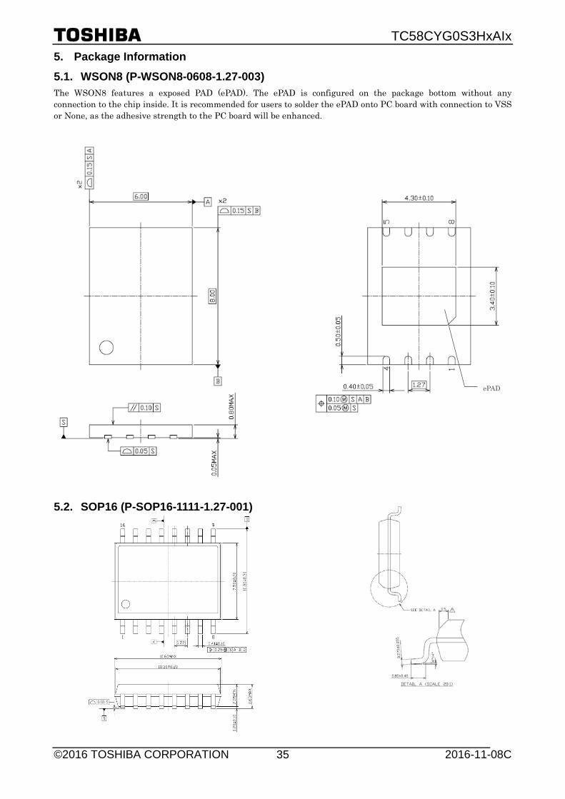
5. Package Information
5.1. WSON8 (P-WSON8-0608-1.27-003) The WSON8 features a exposed PAD (ePAD). The ePAD is configured on the package bottom without any connection to the chip inside. It is recommended for users to solder the ePAD onto PC board with connection to VSS or None, as the adhesive strength to the PC board will be enhanced.
5.2. SOP16 (P-SOP16-1111-1.27-001)
ePAD

TC58CYG0S3HxAIx
©2016 TOSHIBA CORPORATION 2016-11-08C 36
6. Application Notes
6.1. Prohibition of Unspecified Commands The operation commands are listed in Table 11. Input of a command other than those specified in Table 11 is prohibited. Stored data may be corrupted if an unknown command is entered during the command cycle.
6.2. Restriction of Commands while in the Busy State During the operation in progress, do not input any command except Get Feature(0Fh) and Reset(FFh or FEh)
6.3. Addressing for Page Program Operation Within a block, the pages must be programmed consecutively from the LSB (least significant bit) page of the block to MSB (most significant bit) page of the block. Random page address programming is prohibited.
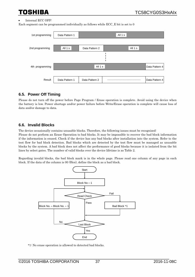
6.4. Several Programming Cycles on the Same Page (Partial Page Program) • Internal ECC ON: Partial Page Program should follow the Table 22 restriction while ECC_E bit is set to 1. ECC Parity Code is generated during program operation on Main area (512 byte) + Spare area (16byte), and this parity code is written to the Parity area as shown in Table 21. For example, each segment can be programmed individually as follows:
DATA IN: Data (1)
Page 0
Data Buffer
Page 2 Page 1
Page 31
Page 63
(1) (2) (3)
(32)
(64)
Data (64)
From the LSB page to MSB page
DATA IN: Data (1)
Page 0
Data Buffer
Page 2 Page 1
Page 31
Page 63
(2) (32) (3)
(1)
(64)
Data (64)
Ex.) Random page program (Prohibition)
TC58CYG0S3HxAIx
©2016 TOSHIBA CORPORATION 2016-11-08C 37
• Internal ECC OFF: Each segment can be programmed individually as follows while ECC_E bit is set to 0
6.5. Power Off Timing Please do not turn off the power before Page Program / Erase operation is complete. Avoid using the device when the battery is low. Power shortage and/or power failure before Write/Erase operation is complete will cause loss of data and/or damage to data.
6.6. Invalid Blocks The device occasionally contains unusable blocks. Therefore, the following issues must be recognized: Please do not perform an Erase Operation to bad blocks. It may be impossible to recover the bad block information if the information is erased. Check if the device has any bad blocks after installation into the system. Refer to the test flow for bad block detection. Bad blocks which are detected by the test flow must be managed as unusable blocks by the system. A bad block does not affect the performance of good blocks because it is isolated from the bit lines by select gates. The number of valid blocks over the device lifetime is as Table 2. Regarding invalid blocks, the bad block mark is in the whole page. Please read one column of any page in each block. If the data of the column is 00 (Hex), define the block as a bad block.
*1: No erase operation is allowed to detected bad blocks.
Pass
Read Check
Start
Bad Block *1
Last Block
End
Yes
Fail
Block No = 1
No
Block No. = Block No. + 1
Data Pattern 4
Data Pattern 1 All 1 s
All 1 s
All 1 s
All 1 s
1st programming
2nd programming
4th programming
Result Data Pattern 1 Data Pattern 2
Data Pattern 4
Data Pattern 2
TC58CYG0S3HxAIx
©2016 TOSHIBA CORPORATION 2016-11-08C 38
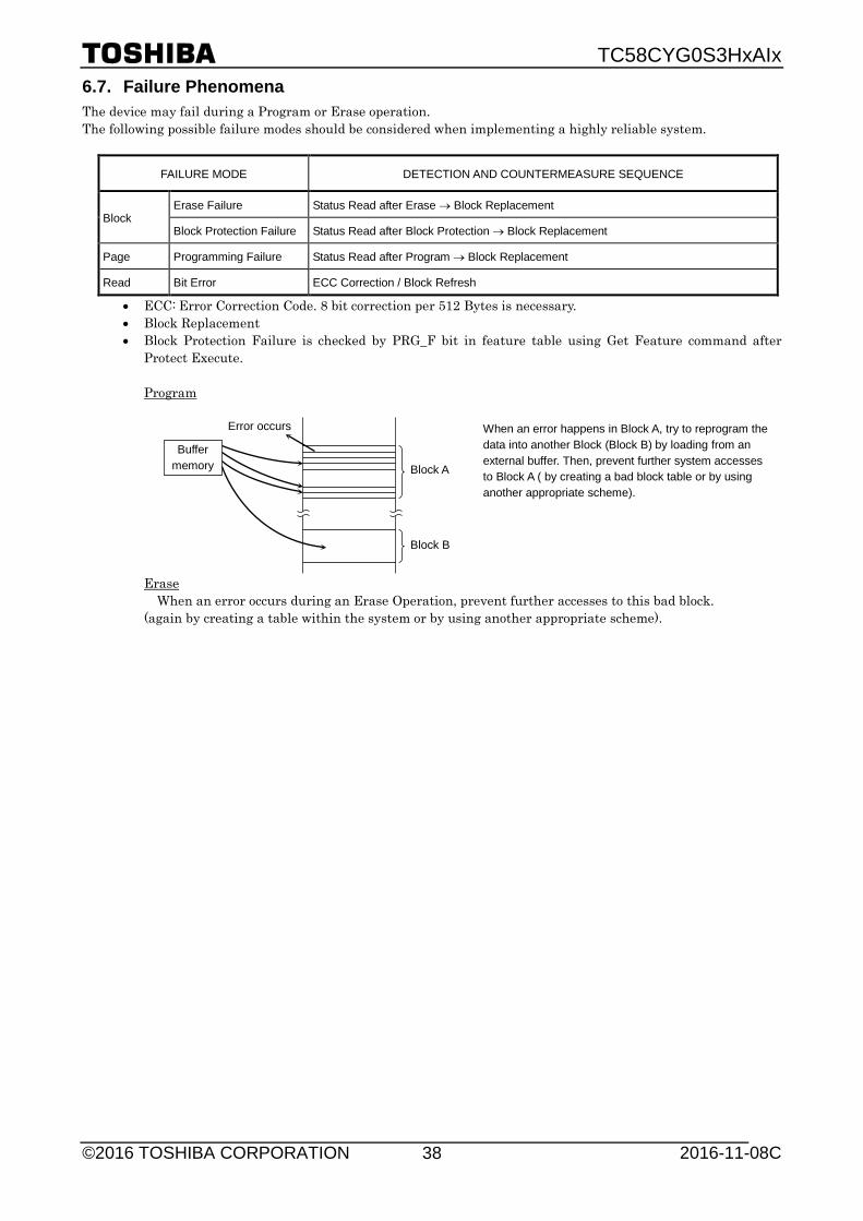
6.7. Failure Phenomena The device may fail during a Program or Erase operation. The following possible failure modes should be considered when implementing a highly reliable system.
FAILURE MODE DETECTION AND COUNTERMEASURE SEQUENCE
Block Erase Failure Status Read after Erase → Block Replacement
Block Protection Failure Status Read after Block Protection → Block Replacement
Page Programming Failure Status Read after Program → Block Replacement
Read Bit Error ECC Correction / Block Refresh
• ECC: Error Correction Code. 8 bit correction per 512 Bytes is necessary. • Block Replacement • Block Protection Failure is checked by PRG_F bit in feature table using Get Feature command after
Protect Execute. Program
Erase When an error occurs during an Erase Operation, prevent further accesses to this bad block.
(again by creating a table within the system or by using another appropriate scheme).
When an error happens in Block A, try to reprogram the data into another Block (Block B) by loading from an external buffer. Then, prevent further system accesses to Block A ( by creating a bad block table or by using another appropriate scheme).
Block A
Block B
Error occurs
Buffer memory

TC58CYG0S3HxAIx
©2016 TOSHIBA CORPORATION 2016-11-08C 39
6.8. Reliability Guidance This reliability guidance is intended to notify some guidance related to using NAND flash with 8 bit ECC for each 512 bytes. For detailed reliability data, please refer to TOSHIBA’s reliability note. Although random bit errors may occur during use, it does not necessarily mean that a block is bad. Generally, a block should be marked as bad when a program status failure or erase status failure is detected. The other failure modes may be recovered by a block erase. ECC treatment for read data is mandatory due to the following Data Retention and Read Disturb failures. • Write/Erase Endurance
Write/Erase endurance failures may occur in a cell, page, or block, and are detected by doing a status read after either an Auto Program or Auto Block Erase operation. The cumulative bad block count will increase along with the number of write/erase cycles.
• Data Retention
The data in memory may change after a certain amount of storage time. This is due to charge loss or charge gain. After block erasure and reprogramming, the block may become usable again.
Here is the combined characteristics image of Write/Erase Endurance and Data Retention. • Read Disturb A Read Operation may disturb the data in memory. The data may change due to charge gain. Usually, bit errors occur on other pages in the block, not the page being read. After a large number of read cycles
(between block erases), a tiny charge may build up and can cause a cell to be soft programmed to another state. After block erasure and reprogramming, the block may become usable again.
Write/Erase Endurance [Cycles]
Data Retention
[Years]

TC58CYG0S3HxAIx
©2016 TOSHIBA CORPORATION 2016-11-08C 40
7. Revision History Date Rev. Description 2016-06-22 1.0 Initial Release. 2016-11-08 1.1 Merged the datasheet of SOP16 and WSON 8 together
Added package code in 1.3. Features. Updated the specification and description in 3.7. Programming, Reading and Erasing Characteristics. Updated the description in 4.2. Page Read Operation, 4.3. Page Read Operation - High Speed Mode, 4.4. Page Program Operation, 4.5. Internal Data Move Operation, 4.6. Block Erase (D8h), 4.7. Reset (FFh or FEh), 4.10. Block Lock Operation, 4.11. Block Protection Operation (One Time Program), 4.12. Parameter Page Read Operation, 4.14. Unique ID Read Operation and 4.16. Internal ECC. Updated 6.4. Several Programming Cycles on the Same Page (Partial Page Program) and 6.7. Failure Phenomena.
TC58CYG0S3HxAIx
©2016 TOSHIBA CORPORATION 2016-11-08C 41
RESTRICTIONS ON PRODUCT USE
• Toshiba Corporation, and its subsidiaries and affiliates (collectively "TOSHIBA"), reserve the right to make changes to the information in this document, and related hardware, software and systems (collectively "Product") without notice.
• This document and any information herein may not be reproduced without prior written permission from TOSHIBA. Even with TOSHIBA's written permission, reproduction is permissible only if reproduction is without alteration/omission.
• Though TOSHIBA works continually to improve Product's quality and reliability, Product can malfunction or fail. Customers are responsible for complying with safety standards and for providing adequate designs and safeguards for their hardware, software and systems which minimize risk and avoid situations in which a malfunction or failure of Product could cause loss of human life, bodily injury or damage to property, including data loss or corruption. Before customers use the Product, create designs including the Product, or incorporate the Product into their own applications, customers must also refer to and comply with (a) the latest versions of all relevant TOSHIBA information, including without limitation, this document, the specifications, the data sheets and application notes for Product and the precautions and conditions set forth in the "TOSHIBA Semiconductor Reliability Handbook" and (b) the instructions for the application with which the Product will be used with or for. Customers are solely responsible for all aspects of their own product design or applications, including but not limited to (a) determining the appropriateness of the use of this Product in such design or applications; (b) evaluating and determining the applicability of any information contained in this document, or in charts, diagrams, programs, algorithms, sample application circuits, or any other referenced documents; and (c) validating all operating parameters for such designs and applications. TOSHIBA ASSUMES NO LIABILITY FOR CUSTOMERS' PRODUCT DESIGN OR APPLICATIONS.
• PRODUCT IS NEITHER INTENDED NOR WARRANTED FOR USE IN EQUIPMENTS OR SYSTEMS THAT REQUIRE EXTRAORDINARILY HIGH LEVELS OF QUALITY AND/OR RELIABILITY, AND/OR A MALFUNCTION OR FAILURE OF WHICH MAY CAUSE LOSS OF HUMAN LIFE, BODILY INJURY, SERIOUS PROPERTY DAMAGE AND/OR SERIOUS PUBLIC IMPACT ("UNINTENDED USE"). Except for specific applications as expressly stated in this document, Unintended Use includes, without limitation, equipment used in nuclear facilities, equipment used in the aerospace industry, medical equipment, equipment used for automobiles, trains, ships and other transportation, traffic signaling equipment, equipment used to control combustions or explosions, safety devices, elevators and escalators, devices related to electric power, and equipment used in finance-related fields. IF YOU USE PRODUCT FOR UNINTENDED USE, TOSHIBA ASSUMES NO LIABILITY FOR PRODUCT. For details, please contact your TOSHIBA sales representative.
• Do not disassemble, analyze, reverse-engineer, alter, modify, translate or copy Product, whether in whole or in part.
• Product shall not be used for or incorporated into any products or systems whose manufacture, use, or sale is prohibited under any applicable laws or regulations.
• The information contained herein is presented only as guidance for Product use. No responsibility is assumed by TOSHIBA for any infringement of patents or any other intellectual property rights of third parties that may result from the use of Product. No license to any intellectual property right is granted by this document, whether express or implied, by estoppel or otherwise.
• ABSENT A WRITTEN SIGNED AGREEMENT, EXCEPT AS PROVIDED IN THE RELEVANT TERMS AND CONDITIONS OF SALE FOR PRODUCT, AND TO THE MAXIMUM EXTENT ALLOWABLE BY LAW, TOSHIBA (1) ASSUMES NO LIABILITY WHATSOEVER, INCLUDING WITHOUT LIMITATION, INDIRECT, CONSEQUENTIAL, SPECIAL, OR INCIDENTAL DAMAGES OR LOSS, INCLUDING WITHOUT LIMITATION, LOSS OF PROFITS, LOSS OF OPPORTUNITIES, BUSINESS INTERRUPTION AND LOSS OF DATA, AND (2) DISCLAIMS ANY AND ALL EXPRESS OR IMPLIED WARRANTIES AND CONDITIONS RELATED TO SALE, USE OF PRODUCT, OR INFORMATION, INCLUDING WARRANTIES OR CONDITIONS OF MERCHANTABILITY, FITNESS FOR A PARTICULAR PURPOSE, ACCURACY OF INFORMATION, OR NONINFRINGEMENT.
• Do not use or otherwise make available Product or related software or technology for any military purposes, including without limitation, for the design, development, use, stockpiling or manufacturing of nuclear, chemical, or biological weapons or missile technology products (mass destruction weapons). Product and related software and technology may be controlled under the applicable export laws and regulations including, without limitation, the Japanese Foreign Exchange and Foreign Trade Law and the U.S. Export Administration Regulations. Export and re-export of Product or related software or technology are strictly prohibited except in compliance with all applicable export laws and regulations.
• Please contact your TOSHIBA sales representative for details as to environmental matters such as the RoHS compatibility of Product. Please use Product in compliance with all applicable laws and regulations that regulate the inclusion or use of controlled substances, including without limitation, the EU RoHS Directive. TOSHIBA ASSUMES NO LIABILITY FOR DAMAGES OR LOSSES OCCURRING AS A RESULT OF NONCOMPLIANCE WITH APPLICABLE LAWS AND REGULATIONS.