Embed Size (px)
Citation preview

Published: September 22, 2011
r 2011 American Chemical Society 4445 dx.doi.org/10.1021/cm201446y |Chem. Mater. 2011, 23, 4445–4451
ARTICLE
pubs.acs.org/cm
Toward Discrete Multilayered Composite Structures: Do HollowNetworks Form in a Polycrystalline Infinite Nanoplane by theKirkendall Effect?Firat G€uder,†,* Yang Yang,†,* Silvana Goetze,‡ Andreas Berger,‡ Roland Scholz,‡ Daniel Hiller,†
Dietrich Hesse,‡ and Margit Zacharias†
†Nanotechnology, Institute of Microsystems Engineering, Faculty of Engineering, Albert-Ludwigs-University of Freiburg,Georges-K€ohler-Allee 103, D-79110 Freiburg, Germany‡Max Planck Institute of Microstructure Physics, Weinberg 2, D-06120 Halle, Germany
’ INTRODUCTION
In recent years, the nanoscale Kirkendall effect has extensivelybeen utilized to produce a variety of hollow nanospheres,nanotubes, hollow/porous hierarchical nanostructures, and evenmore.1�7 This fabrication regime involves unequal atomic diffu-sivities across a binary-phase interface, and is compensated by theinjection of lattice vacancies that can accumulate and super-saturate into voids near the interface along the side of the fasterdiffusing species. Core�shell nanowires/nanospheres have twoor all three dimensions at the nanoscale. Injected vacancies inthese confined spaces are easy to supersaturate and accumulateinto single voids. Consequently, nanotubes and hollow nano-spheres can evolve from the initial core�shell nanostructures,exploiting the nanoscale Kirkendall void formation process.
The established knowledge on the interdiffusion behavior ofdiverse binary thin-film diffusion couples provides a rich databasefor rational selection and design of core�shell precursors withunequal diffusion coefficients. However, for structures directlyderived from film stacking, for example, binary nanoscale
multilayered systems with alternating A and B layers, it has notbeen revealed until now how the Kirkendall void formation isevolved. In contrast to core�shell nanostructures, binary nano-scale multilayered systems have only one dimensional parameterat the nanoscale (the respective layer thickness), whereas theother dimensions are infinitely extended. Besides a large diffusioninterface area,8,9 another distinct feature of the multilayeredsystems is that film stacks grown by current deposition techni-ques frequently encounter a polycrystalline structure. The widenetwork of short circuit diffusion paths composed of grainboundaries (GBs) should play a crucial role during the thermalinterdiffusion process.10 Therefore, the void formation regimescan be significantly different from the core�shell nanowires/nanospheres normally representing an encapsulated single-crystal core.
Received: May 23, 2011Revised: August 7, 2011
ABSTRACT: Spatial confinement in nanostructures is of critical im-portance in the fabrication of tubular and hollow spherical objects usingvoid formation via the Kirkendall effect. For both core�shell nanowiresand nanospheres, generated vacancies are trapped within an area that isconfined either in two (nanowires) or all three (nanospheres) spatialdimensions. When the void formation is extended to multilayered thinfilms where only one dimension (thickness) is in the nanoscale and theother dimensions are infinitely extended, the final morphology of theformed voids can be significantly different. Using a multilayered systemconsisting of alternating layers of ZnO and Al2O3 grown by atomic layerdeposition (ALD), we investigate the effects of annealing temperature,annealing duration, layer thickness, polycrystallinity, grain size, andreaction space on the solid-state diffusion process and final morphologyof the produced Kirkendall voids. As opposed to single-crystal ZnO nanowires coated with an amorphous Al2O3 shell, whichinvolves only a one-way transfer of ZnO into Al2O3, polycrystalline ZnO layers in themultilayered films also cause diffusion of Al2O3
into ZnO layers via grain boundary diffusion. Temperature treatment at 700 �C generally yielded layered voids for multilayered filmswith thin component sublayers. This morphology was well-preserved even at 800 �C. In contrast, partially continuous nanogapmorphologies were formed for multilayered films with thick sublayers at 700 �C. However, only interlaced voids were produced at800 �C in this case, because of grain boundary migration induced oriented attachment. The mechanisms revealed here allow precisefabrication and design of porous multilayered composite films with controlled void morphology.
KEYWORDS: multilayered structure, Kirkendall effect, grain boundary diffusion, grain boundary migration, oriented attachment

4446 dx.doi.org/10.1021/cm201446y |Chem. Mater. 2011, 23, 4445–4451
Chemistry of Materials ARTICLE
By using single-crystal ZnO nanowires coated with an amor-phous Al2O3 layer, our group has studied the reaction mechan-isms and various other factors influencing the thermal diffusionprocess in ZnO�Al2O3 core�shell nanowires in detail.11�14 Itwas revealed that the bulk solubility of Al2O3 in ZnO is almostzero at elevated temperatures and the solubility of ZnO in Al2O3
is very high. This example represents an extreme Kirkendall typediffusion process as it is effectively a one-way outward diffusionof ZnO into Al2O3, accompanied by the formation of spinelZnAl2O4.
In this article, we extend this thermal diffusion couple and useperiodically alternating Al2O3 and ZnO layers as a modelstructure to investigate the unequal interdiffusion process innanoscale multilayered systems. The intended Al2O3/ZnO mul-tilayered structure consists in total of nine alternating layers (fiveAl2O3 and four ZnO) sequentially grown by atomic layerdeposition (ALD). The Al2O3 layers are amorphous in naturewhile the ZnO layers are polycrystalline. We explore the possi-bility of applying the nanoscale Kirkendall effect in a polycrystal-line infinite space for the fabrication of discrete ZnAl2O4
multilayered structures. Depending on the process parameterssuch as annealing time, reaction temperature, and film thickness,ordered/unordered embedded cavities or partially continuouslarge gaps are formed. The results indicate that the voidmorphology in the final spinel ZnAl2O4 products can be effec-tively regulated. These findings are further extended to variousAl2O3/ZnO multilayered 1D nanosystems to instruct the fabri-cation of complex 1D porous nanostructures. This case study isof particular importance for producing layered compounds andporous thin films derived from Kirkendall-type thin-film diffu-sion couples, and for increasing the experimental predictability oftarget nanostructures.
’EXPERIMENTAL SECTION
Al2O3/ZnO multilayered films, consisting of five layers of Al2O3 andfour layers ZnO, were deposited by atomic layer deposition at 150 �C(Oxford Instruments, OpAL) on 1%HF treated Si (100) substrates. Thethickness of each Al2O3 and ZnO layer was precisely controlled by thenumber of diethylzinc (DEZ)/H2O and trimethylaluminum (TMA)/H2Oexposure cycles. The pulse length for DEZ and TMAwere set to 40 and 20ms, respectively. After each metalorganic precursor pulse, a 20 ms dose ofH2O was released into the reactor as the oxidant. Before deposition, thereactor was pumped down to 8 mTorr and maintained between 170 and190 mTorr during the process. N2 gas was used as the purging agent toremove any residual/byproduct gases to prevent parasitic reactions.The long time anneals at 700 and 800 �C in air were performed using a
standard box furnace manufactured by Carbolite. The short time annealswere performed in a rapid thermal processing furnace (Jipelec JetFirst200C).ZnAl2O4 nanotube templates were fabricated using ZnO/Al2O3
core�shell nanowires and annealing them at 800 �C in air. Commer-cially available multiwall carbon nanofibers were purchased fromNanothinx, Greece. ZnO nanowires were grown via a vapor transporttechnique on silicon or GaN/sapphire substrates using gold as catalyst.ZnO (Sigma Aldrich 99.999%) and graphite (Alfa/Aesar ∼200 mesh)powders were used as source, mixed in a 1:1 ratio. The substrate wasplaced near the source powder in a quartz tube furnace. The pressureinside the tube was maintained at 200 mbar using O2 (0.001 sccm) andAr (7 sccm) as carrier gases and a growth temperature between 875 and939 �C was maintained.The ZnAl2O4 nanotube templates were coated with a single layer of
ZnO (12 nm) and an Al2O3 (24 nm). The coated templates were then
annealed at 700 �C in air. Carbon nanofibers were coated with a triplelayered film stack consisting of a single layer of 12 nm ZnO layersandwiched between two 24 nm Al2O3 layers and the final structure wasannealed at again 700 �C in air. And finally, ZnO nanowires with a TiO2
diffusion barrier shell were coated with a nine layer multilayered filmwith alternating layers of ZnO (four layers of 12 nm) and Al2O3 (fivelayers of 24 nm) films, which were subsequently annealed at 800 �C.
Cross-sectional TEM samples were prepared by the standard pre-paration technique. A stack was first made by gluing together twosubstrate fragments (film-to-film). After the mechanical thinning downprocess (mechanical polishing), final thinning was done with the help ofion milling. The cross-sectional TEM samples were analyzed using twotransmission electron microscopes, viz. a CM20T from Philips (200 kV)and a JEM-4010 from JEOL (400 kV) for high resolution TEMmicrographs. A Philips CM20FEG scanning TEM instrument (200kV) equipped with an EDXdetector (IDFix-system, SAMx) was used forenergy-dispersive X-ray spectroscopy analysis. 1D nanostructures wereobserved by a JEOL JEM-1010 electron microscope (100 kV).
’RESULTS AND DISCUSSION
Growth of Al2O3/ZnO Multilayered Films by ALD. A sche-matic view of the ALD-grown Al2O3/ZnO multilayered films isshown in Figure 1a. ALD, a gas phase deposition technique, hasbeen widely used to produce thin-film structures for variousapplications. Unlike conventional chemical vapor deposition(CVD), in a typical ALD process, the reaction gases are releasedinto the deposition chamber separately, in a self-limiting andalternating manner. This property of the ALD process ensuresprecise monolayer thickness control and allows deposition ofvarious high-quality and conformal binary oxides, sulfides, metalsand other binary/ternary materials in a wide temperaturewindow.15�18 In our experiments, Si (100) wafers were selectedas the substrate material because no major interdiffusion occursbetween the Si substrate and the ALD-deposited Al2O3 films attemperatures even as high as 1200 �C.19 Therefore, the bottomAl2O3 layer is a good diffusion barrier to prevent interactionswith the underlying substrate. For studying the effects of layerthickness/grain size on the Kirkendall void formation in multi-layered films, we prepared two different multilayered samples,namely sample I and sample II, for the subsequent solid-statereactions. For both cases, a thickness ratio of 2:1 for Al2O3:ZnOwas employed to ensure complete consumption of each ZnOlayer in the ZnAl2O4-forming reaction at high temperatures.Figures 1b, c present a typical cross-sectional transmissionelectron microscopy (TEM) image of the samples I and II,respectively, in which the dark segments correspond to ZnO andthe light ones to Al2O3. Sample I consists of alternating layers of12 nm Al2O3 and 6 nm ZnO. Sample II has exactly the samegeometry except the layer thicknesses are doubled to 24 nm(Al2O3) and 12 nm (ZnO). Panels d and e in Figure 1 exhibit theresult of a TEM-EDX (energy-dispersive X-ray spectroscopy)line scan performed across the cross-section of sample II. It canbe clearly seen that abrupt changes occur in the detected Al andZn levels indicating that the deposited layers have indeed amultilayered sequence with sharp junctions. It is known that theAl2O3 films deposited in a wide temperature window by ALD areamorphous. However, ZnO films produced by ALD are alwayscrystalline regardless of the deposition temperature. To investi-gate the thickness relationship of the ALD-deposited ZnO filmswith crystalline properties, single-crystal ZnO nanowires werealso used as substrates for the ALD deposition of ZnO layers, to

4447 dx.doi.org/10.1021/cm201446y |Chem. Mater. 2011, 23, 4445–4451
Chemistry of Materials ARTICLE
facilitate direct and timely TEM observations. A TEM image ofZnO nanowires coated with a 5 nm ZnO film is displayed inFigure 1f (bottom). The rough surface of the resulting nanowiredemonstrates that the ZnO film deposited at a temperature ofaround 150 �C is actually composed ofmany tiny crystallites. Thetop image (Figure 1f) shows the electron diffraction patternobtained from this nanowire. The simultaneous presence of theindexed diffraction rings confirms the polycrystalline nature ofthe ALD-deposited ZnO film. When the thickness of thedeposited film was increased to 25 nm, larger ZnO crystalliteswere abundantly formed, as shown in Figure 1f. This resultindicates that the crystallite size in the ALD-deposited ZnO filmsincreases with thickness, most possibly due to Ostwald ripening.Kirkendall Void Formation in the Al2O3/ZnO Multilayered
Films.For inducing thermal diffusion of the ZnO layers into theiradjacent Al2O3 layers, both sample I and sample II were annealedat elevated temperatures in air. Figure 2a shows a cross-sectionalTEMmicrograph of sample I upon annealing at 700 �C for 3 h. Itis found that partially continuous nanogaps occurred in place ofthe original ZnO layers. This process is governed by the reactiveKirkendall-type diffusion of ZnO into Al2O3, consistent with ourprevious results on the formation of spinel ZnAl2O4 nanotubesby the solid�solid reaction of ZnO�Al2O3 core�shell nano-wires. However, the nanogaps are not completely continuouseven if all the ZnO layers are supposed to be entirely consumedfrom a chemical viewpoint. The formation of completely con-tinuous nanogaps may have been prevented by the extent of thesolid�solid reaction space, which is not confined to a small areaas in core�shell nanostructures. Aside from the reaction space,due to dimensions of the deposited thin films, infinitely large andfreestanding layers may not be thermally stable as these discretefilms would require the means of mechanical support. In the caseof ZnO�Al2O3 core�shell nanowires, the generated vacanciesmore easily accumulate and grow into large voids, and finallyevolve into nanotubes due to confined reaction space between
the reactants as well as the resultant self-supportive tubularstructure. When the temperature was raised to 800 �C, thediscontinuous morphology feature of the formed nanogaps wasamplified and layers of ordered nanocavities appeared(Figure 2b). Especially, the nanocavities seem to have the shapeof the initial ZnO nanocrystals, differing from both the interfacialvoids evolving by surface diffusion of the Kirkendall voids in theZnO�Al2O3 core�shell nanowires, and those created by thesimple decay of the neighboring spinel layers owing to thermalinstability.12 Peng et al. once produced nanolaminate assembliesof Al2O3/ZnO/Al2O3 trilayers and investigated the bidirectionaldiffusion of ZnO based on the Kirkendall effect.20 This studygranted that the polycrystalline ZnO thin films behave the sameway as single-crystal ZnO substrates during a spinel-formingthermal diffusion process. However, in the current experiments,we demonstrated that the polycrystalline nature of ZnO in themultilayered films cannot be ignored.In the multilayered films, the polycrystalline ZnO layers intro-
duce many short-circuit diffusion paths via the grain boundary(GB) network.10 The GBs could easily accommodate diffusion ofAl2O3 into ZnO layers, since GB diffusivity is much larger thanbulk/lattice diffusivity.21 The preferential GB diffusion of Al2O3
causes encapsulation of ZnO crystals, freezing them in their initialpositions. Then, the solid�solid ZnAl2O4-forming reaction
Figure 1. (a) Schematic diagram of multilayered film grown by ALD.Cross-sectional TEM micrographs of (b) sample I consisting of fivelayers of Al2O3 (12 nm, light contrast) and four layers of ZnO (6 nm,dark contrast), and (c) sample II consisting of five layers of Al2O3
(24 nm, light contrast) and four layers of ZnO (12 nm, dark contrast).(d) Cross-sectional TEMmicrograph of sample II showing the scan linefor EDX analysis. (e) EDX results from the line scan shown in d. (f) ZnOnanowires coated with 5 and 25 nm ALD ZnO. Inset is the electrondiffraction pattern from the nanowire coated with 5 nm ALD ZnO.
Figure 2. Cross-sectional TEM micrographs of sample I (a) afterannealing for 3 h at 700 �C in air, (b) after annealing for 3 h at 800 �Cin air, (c) after RTP treatment for 1 min at 800 �C in air.
4448 dx.doi.org/10.1021/cm201446y |Chem. Mater. 2011, 23, 4445–4451
Chemistry of Materials ARTICLE
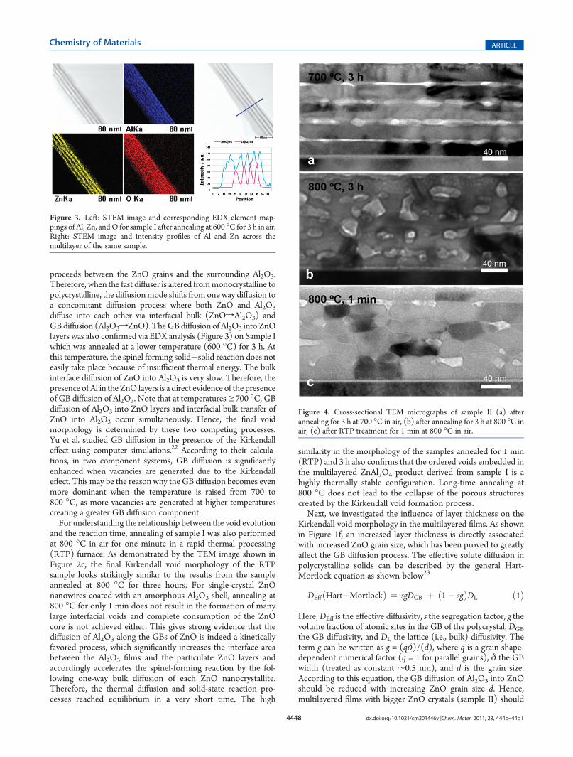
proceeds between the ZnO grains and the surrounding Al2O3.Therefore, when the fast diffuser is altered frommonocrystalline topolycrystalline, the diffusionmode shifts from one way diffusion toa concomitant diffusion process where both ZnO and Al2O3
diffuse into each other via interfacial bulk (ZnOfAl2O3) andGBdiffusion (Al2O3fZnO).TheGBdiffusion ofAl2O3 intoZnOlayers was also confirmed via EDX analysis (Figure 3) on Sample Iwhich was annealed at a lower temperature (600 �C) for 3 h. Atthis temperature, the spinel forming solid�solid reaction does noteasily take place because of insufficient thermal energy. The bulkinterface diffusion of ZnO into Al2O3 is very slow. Therefore, thepresence of Al in the ZnO layers is a direct evidence of the presenceof GB diffusion of Al2O3. Note that at temperaturesg700 �C, GBdiffusion of Al2O3 into ZnO layers and interfacial bulk transfer ofZnO into Al2O3 occur simultaneously. Hence, the final voidmorphology is determined by these two competing processes.Yu et al. studied GB diffusion in the presence of the Kirkendalleffect using computer simulations.22 According to their calcula-tions, in two component systems, GB diffusion is significantlyenhanced when vacancies are generated due to the Kirkendalleffect. This may be the reason why the GB diffusion becomes evenmore dominant when the temperature is raised from 700 to800 �C, as more vacancies are generated at higher temperaturescreating a greater GB diffusion component.For understanding the relationship between the void evolution
and the reaction time, annealing of sample I was also performedat 800 �C in air for one minute in a rapid thermal processing(RTP) furnace. As demonstrated by the TEM image shown inFigure 2c, the final Kirkendall void morphology of the RTPsample looks strikingly similar to the results from the sampleannealed at 800 �C for three hours. For single-crystal ZnOnanowires coated with an amorphous Al2O3 shell, annealing at800 �C for only 1 min does not result in the formation of manylarge interfacial voids and complete consumption of the ZnOcore is not achieved either. This gives strong evidence that thediffusion of Al2O3 along the GBs of ZnO is indeed a kineticallyfavored process, which significantly increases the interface areabetween the Al2O3 films and the particulate ZnO layers andaccordingly accelerates the spinel-forming reaction by the fol-lowing one-way bulk diffusion of each ZnO nanocrystallite.Therefore, the thermal diffusion and solid-state reaction pro-cesses reached equilibrium in a very short time. The high
similarity in the morphology of the samples annealed for 1 min(RTP) and 3 h also confirms that the ordered voids embedded inthe multilayered ZnAl2O4 product derived from sample I is ahighly thermally stable configuration. Long-time annealing at800 �C does not lead to the collapse of the porous structurescreated by the Kirkendall void formation process.Next, we investigated the influence of layer thickness on the
Kirkendall void morphology in the multilayered films. As shownin Figure 1f, an increased layer thickness is directly associatedwith increased ZnO grain size, which has been proved to greatlyaffect the GB diffusion process. The effective solute diffusion inpolycrystalline solids can be described by the general Hart-Mortlock equation as shown below23
DEff ðHart�MortlockÞ ¼ sgDGB þ ð1� sgÞDL ð1Þ
Here,DEff is the effective diffusivity, s the segregation factor, g thevolume fraction of atomic sites in the GB of the polycrystal, DGB
the GB diffusivity, and DL the lattice (i.e., bulk) diffusivity. Theterm g can be written as g = (qδ)/(d), where q is a grain shape-dependent numerical factor (q = 1 for parallel grains), δ the GBwidth (treated as constant ∼0.5 nm), and d is the grain size.According to this equation, the GB diffusion of Al2O3 into ZnOshould be reduced with increasing ZnO grain size d. Hence,multilayered films with bigger ZnO crystals (sample II) should
Figure 3. Left: STEM image and corresponding EDX element map-pings of Al, Zn, andO for sample I after annealing at 600 �C for 3 h in air.Right: STEM image and intensity profiles of Al and Zn across themultilayer of the same sample.
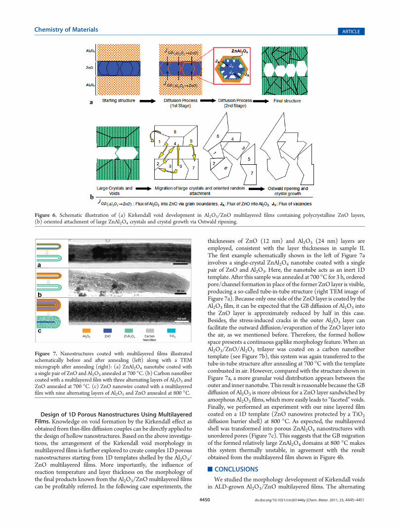
Figure 4. Cross-sectional TEM micrographs of sample II (a) afterannealing for 3 h at 700 �C in air, (b) after annealing for 3 h at 800 �C inair, (c) after RTP treatment for 1 min at 800 �C in air.

4449 dx.doi.org/10.1021/cm201446y |Chem. Mater. 2011, 23, 4445–4451
Chemistry of Materials ARTICLE
show a better gap profile than sample I at lower temperaturessuch as 700 �C because the increased grain size of ZnO canreduce the GB diffusion of Al2O3.To confirm these assumptions, sample II was subjected to the
same thermal processes as sample I. First, sample II was annealedat 700 �C for 3 h. The resulting pore morphology is shown inFigure 4a. Under these annealing conditions, long and partiallysegmented nanogaps were formed. The pore morphology re-sembles the results obtained from sample I at 700 �C but thistime the gaps seem to have a more continuous profile. When thethermal process was repeated at 800 �C for 3 h, the multilayeredfilm unexpectedly transformed into a ZnAl2O4 film with arandom, unordered pore morphology with unexpectedly largecavities as shown in Figure 4b. To understand the source of thelarge voids and the random pore morphology, sample II was alsosubjected to a 1 min RTP anneal in air at 800 �C. The resultingstructure, see Figure 4c, is an intermediate, nonequilibrium stagein the thermal process, where large spinel crystals are clearlyvisible. The formation of large spinel crystals during the solid�solid reaction is not surprising due to the larger size of the initialZnO crystals in sample II. It appears that the formed voids travelthrough the ZnAl2O4 GB network, settle and enlarge in energe-tically favorable sinks, which leads to formation of large inter-laced voids in the film. Although increased grain size of ZnOreduces the influence of Al2O3 GB diffusion into the ZnO layers,the ordered gap morphology decayed at higher temperaturessuch as 800 �C because of lower porosity and enhanced GBmigration of the formed ZnAl2O4.
10
Figure 5 shows a series of high-resolution TEM (HRTEM)images of sample II after the RTP treatment at 800 �C. Figure 5arepresents a low-magnification TEM micrograph belonging tothis sample. Various sites are selected from this sample forHRTEM analysis to determine the underlying cause of the
randomly ordered void morphology. Interestingly, even thoughthe sample consists of randomly ordered large voids, relativelylong, partially continuous gap formations are visible beneath thetop layer. This is also the case for sample I thermally treated byRTP at 800 �C for 1 min. The HRTEMmicrograph in Figure 5bdemonstrates that the top first layer is composed of long-sectional monocrystalline ZnAl2O4. The distinctive gap-likemorphology under this ZnAl2O4 cap indicates that the diffusionbehavior of the ZnO top layer is different from that of the otherlayers. It is reasonable to consider that the sandwiched ZnO toplayer is not really embedded during the RTP-induced solid�solidreaction because the stress-induced cracks in the top Al2O3 layercan facilitate its outward diffusion/evaporation into the air.13
Figure 5c shows two large adjacent ZnAl2O4 bicrystals locatedinside the multilayered film. The crystals are attached to oneanother with a small angle α with the same crystal facets facingeach other. This result suggests that large crystals in the ZnAl2O4
film having clear facets can approach, attach, and fuse each otherin an oriented manner during thermal annealing at highertemperatures.24 The GB migration of the formed ZnAl2O4
domains could be triggered and enhanced by the increasedmechanical stress within the multilayered film due to largeroverall film thickness and lower porosity due to increased ZnOgrain size.10,25 Moreover, large nanocrystallites are known to bebetter faceted than small ones. For instance, very small Aunanocrystals are approximately spherical in shape, forming noclear facets but this is not the case when the crystal size isincreased. Thus, when sample I was annealed under the sameconditions as sample II, ordered voidmorphology was retained asa result of smaller overall multilayered film thickness and higherporosity which prevented major GB migration. Additionally,large spinel grains forming across the multilayer stack wereoccasionally observed in sample I after annealing at 800 �C, asshown in Figure 2b. These large crystals were most probablyproduced by the fusion of small immobile adjacent grainsannealed at such a high temperature. The ordered void mor-phology in the multilayer stack is not disturbed in the presenceof these large crystals, suggesting the absence of major grainboundary migration during the reaction. In contrast, thesereconfiguration processes became severe and widespread whenthe film thickness and ZnO grain size were increased (sample II).Figure 5d shows bicrystals that are again attached in an orientedmanner. Because this time the attachment angle is zero and thegrains are well-aligned, if annealed further, these crystals willmost likely fuse and grow into a bigger crystal.26
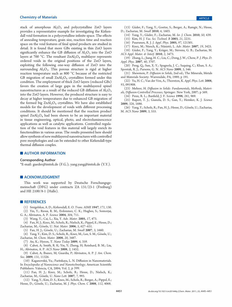
A schematic summary of the Kirkendall void development inour multilayered films is presented in Figure 6. The overall voidevolution can be considered as a two stage process (Figure 6a). Inthe first stage, Al2O3 diffuses into ZnO via GBs surrounding theZnO nanocrystals in the layers. In the second stage, ZnO diffusesinto the surrounding Al2O3 through the interface via bulkdiffusion which results in inward injection of vacancies andformation of embedded ordered Kirkendall voids. If the initialZnO layers in the multilayered film are thick, the GB diffusion ofAl2O3 into ZnO is partially weakened because of increased grainsize. Better gaplike layered nanostructures are formed, accom-panying the formation of large ZnAl2O4 crystals. However,increased mechanical stress, reduced porosity, and well-facetedcrystallite morphology in this case very easily initiate GB migra-tion of the formed ZnAl2O4 crystals at higher temperatures andlead to degradation of the layered structures. Such a structuraldevelopment process is schemed in Figure 6b.
Figure 5. (a) Low-magnification TEM image of sample II annealed for1 min at 800 �C in air. High-resolution TEM micrographs of (b) topZnAl2O4 spinel layer, (c) adjacent bicrystals attached with an angle α,(d) adjacent bicrystals attached without an angle. Note that dashed linesare the grain boundaries.
4450 dx.doi.org/10.1021/cm201446y |Chem. Mater. 2011, 23, 4445–4451
Chemistry of Materials ARTICLE
Design of 1D Porous Nanostructures Using MultilayeredFilms. Knowledge on void formation by the Kirkendall effect asobtained from thin-film diffusion couples can be directly applied tothe design of hollow nanostructures. Based on the above investiga-tions, the arrangement of the Kirkendall void morphology inmultilayered films is further explored to create complex 1D porousnanostructures starting from 1D templates shelled by the Al2O3/ZnO multilayered films. More importantly, the influence ofreaction temperature and layer thickness on the morphology ofthe final products known from the Al2O3/ZnOmultilayered filmscan be profitably referred. In the following case experiments, the
thicknesses of ZnO (12 nm) and Al2O3 (24 nm) layers areemployed, consistent with the layer thicknesses in sample II.The first example schematically shown in the left of Figure 7ainvolves a single-crystal ZnAl2O4 nanotube coated with a singlepair of ZnO and Al2O3. Here, the nanotube acts as an inert 1Dtemplate. After this sample was annealed at 700 �C for 3 h, orderedpore/channel formation in place of the former ZnO layer is visible,producing a so-called tube-in-tube structure (right TEM image ofFigure 7a). Because only one side of the ZnO layer is coated by theAl2O3 film, it can be expected that the GB diffusion of Al2O3 intothe ZnO layer is approximately reduced by half in this case.Besides, the stress-induced cracks in the outer Al2O3 layer canfacilitate the outward diffusion/evaporation of the ZnO layer intothe air, as we mentioned before. Therefore, the formed hollowspace presents a continuous gaplike morphology feature.When anAl2O3/ZnO/Al2O3 trilayer was coated on a carbon nanofibertemplate (see Figure 7b), this system was again transferred to thetube-in-tube structure after annealing at 700 �C with the templatecombusted in air. However, compared with the structure shown inFigure 7a, a more granular void distribution appears between theouter and inner nanotube. This result is reasonable because theGBdiffusion of Al2O3 is more obvious for a ZnO layer sandwiched byamorphous Al2O3 films, whichmore easily leads to “faceted” voids.Finally, we performed an experiment with our nine layered filmcoated on a 1D template (ZnO nanowires protected by a TiO2
diffusion barrier shell) at 800 �C. As expected, the multilayeredshell was transformed into porous ZnAl2O4 nanostructures withunordered pores (Figure 7c). This suggests that the GBmigrationof the formed relatively large ZnAl2O4 domains at 800 �C makesthis system thermally unstable, in agreement with the resultobtained from the multilayered film shown in Figure 4b.
’CONCLUSIONS
We studied the morphology development of Kirkendall voidsin ALD-grown Al2O3/ZnO multilayered films. The alternating
Figure 6. Schematic illustration of (a) Kirkendall void development in Al2O3/ZnO multilayered films containing polycrystalline ZnO layers,(b) oriented attachment of large ZnAl2O4 crystals and crystal growth via Ostwald ripening.
Figure 7. Nanostructures coated with multilayered films illustratedschematically before and after annealing (left) along with a TEMmicrograph after annealing (right): (a) ZnAl2O4 nanotube coated witha single pair of ZnO and Al2O3 annealed at 700 �C. (b) Carbon nanofibercoated with a multilayered film with three alternating layers of Al2O3 andZnO annealed at 700 �C. (c) ZnO nanowire coated with a multilayeredfilm with nine alternating layers of Al2O3 and ZnO annealed at 800 �C.
4451 dx.doi.org/10.1021/cm201446y |Chem. Mater. 2011, 23, 4445–4451
Chemistry of Materials ARTICLE
stack of amorphous Al2O3 and polycrystalline ZnO layersprovides a representative example for investigating the Kirken-dall void formation in a polycrystalline infinite space. The effectsof annealing temperature, grain size, reaction time and reactionspace on the void features of final spinel products are studied indetail. It is found that more GBs existing in thin ZnO layerssignificantly enhance the GB diffusion of Al2O3 into the ZnOlayers at 700 �C. The resultant ZnAl2O4 multilayer representsordered voids in the original positions of the ZnO layers,exploiting the following one-way diffusion of ZnO into thesurrounding Al2O3. This porous structure is rigid at higherreaction temperature such as 800 �C because of the restrictedGB migration of small ZnAl2O4 crystallites formed under thiscondition. The employment of thick ZnO layers (reduced GBs)favors the creation of large gaps in the multilayered spinelnanostructures as a result of the reduced GB diffusion of Al2O3
into the ZnO layers. However, the produced structure is easy todecay at higher temperatures due to enhanced GB migration ofthe formed big ZnAl2O4 crystallites. We have also establishedmodels for the development of voids with different processingconditions. It should be mentioned that the reaction productspinel ZnAl2O4 had been shown to be an important materialin tissue engineering, optical, photo, and electroluminescenceapplications as well as catalytic applications. Controlled regula-tion of the void features in this material will largely enrich itsfunctionalities in various areas. The results presented here shouldallow synthesis of newmultilayered nanostructures with controlledpore morphologies and can be extended to other Kirkendall-typethermal diffusion couples.
’AUTHOR INFORMATION
Corresponding Author*E-mail: [email protected] (F.G.); [email protected] (Y.Y.).
’ACKNOWLEDGMENT
This work was supported by Deutsche Forschungsge-meinschaft (DFG) under contracts ZA 131/23-1 (Freiburg)and HE 2100/8-1 (Halle).
’REFERENCES
(1) Smigelskas, A. D.; Kirkendall, E. O. Trans. AIME 1947, 171, 130.(2) Yin, Y.; Rioux, R. M.; Erdonmez, C. K.; Hughes, S.; Somorjai,
G. A.; Alivisatos, A. P. Science 2004, 304, 711.(3) Wang, Y.; Cai, L.; Xia, Y. Adv. Mater. 2005, 17, 473.(4) Fan, H. J.; Knez,M.; Scholz, R.; Nielsch, K.; Pippel, E.; Hesse, D.;
Zacharias, M.; G€osele, U. Nat. Mater. 2006, 5, 627–631.(5) Fan, H. J.; G€osele, U.; Zacharias, M. Small 2007, 3, 1660.(6) Yang, Y.; Kim, D. S.; Scholz, R.; Knez, M.; Lee, S. M.; G€osele, U.;
Zacharias, M. Chem. Mater. 2008, 20, 3487.(7) An, K.; Hyeon, T. Nano Today 2009, 4, 359.(8) Cabot, A; Smith, R. K; Yin, Y; Zheng, H; Reinhard, B. M.; Liu,
H.; Alivisatos, A. P. ACS Nano 2008, 2, 1452.(9) Cabot, A; Ibanez, M; Guardia, P; Alivisatos, A. P. J. Am. Chem.
Soc. 2009, 131, 11326.(10) Kaganovskii, Yu.; Paritskaya, L. N. Diffusion in Nanomaterials.
In Encyclopedia of Nanoscience and Nanotechnology; American ScientificPublishers: Valencia, CA, 2004; Vol. 2, p 399.(11) Fan, H. J.; Knez, M.; Scholz, R.; Hesse, D.; Nielsch, K.;
Zacharias, M.; G€osele, U. Nano Lett. 2007, 7, 993.(12) Yang, Y.; Kim, D. S.; Knez, M.; Scholz, R.; Berger, A.; Pippel, E.;
Hesse, D.; G€osele, U.; Zacharias, M. J. Phys. Chem. C 2008, 112, 4068.
(13) G€uder, F.; Yang, Y.; Goetze, S.; Berger, A.; Ramgir, N.; Hesse,D.; Zacharias, M. Small 2010, 6, 1603.
(14) Yang, Y.; G€uder, F.; Zacharias, M. Isr. J. Chem. 2010, 50, 439.(15) Kim, H. J. Vac. Sci. Technol. B 2003, 21, 2231.(16) Puurunen, R. J. J. Appl. Phys. 2005, 97, 121301.(17) Knez, M.; Niesch, K.; Niinist€o, L. Adv. Mater. 2007, 19, 3425.(18) G€uder, F.; Yang, Y.; Kr€uger, M.; Stevens, G. B.; Zacharias, M.
ACS Appl. Mater. & Interf. 2010, 2, 3473.(19) Zhang, L.; Jiang, H. C.; Liu, C.; Dong, J. W.; Chow, P. J. Phys. D:
Appl. Phys. 2007, 40, 3707.(20) Peng, Q.; Sun, X.-Y.; Spagnola, J. C.; Saquing, C.; Khan, S. A.;
Spontak, R. J.; Parsons, G. N. ACS Nano 2009, 3, 546.(21) Shewmon, P. Diffusion in Solids, 2nd ed.; The Minerals, Metals
and Materials Society: Warrendale, PA, 1989; p 191.(22) Yu, H. C.; Van der Ven, A.; Thornton, K. Appl. Phys. Lett. 2008,
93, 091908.(23) Mehrer, H. Diffusion in Solids: Fundamentals, Methods, Materi-
als, Diffusion-Controlled Processes; Springer: New York, 2007; p 569.(24) Penn, R. L.; Banfield, J. F. Science 1998, 281, 969.(25) Rupert, T. J.; Gianola, D. S.; Gan, Y.; Hemker, K. J. Science
2009, 326, 1686.(26) Yang, Y.; Scholz, R.; Fan, H. J.; Hesse, D.; G€osele, U.; Zacharias,
M. ACS Nano 2009, 3, 555.

![Flexural properties of sawdust reinforced phenolic …...application of phenolic resins is for inner lining of multilayered composite in fire critical applications [4, 5]. By varying](https://img.pdfslide.net/doc/110x75/610c975d1be80b0eef4ccd84/flexural-properties-of-sawdust-reinforced-phenolic-application-of-phenolic-resins.jpg)