Embed Size (px)
Citation preview

Towards Achieving Highly Parallelized Publish/SubscribeMatching at Line-Rates Using Reconfigurable Hardware
by
Harshvardhan Pratap Singh
A thesis submitted in conformity with the requirementsfor the degree of Master of Applied Science
Graduate Department of Electrical and Computer EngineeringUniversity of Toronto
Copyright c© 2011 by Harshvardhan Pratap Singh

Abstract
Towards Achieving Highly Parallelized Publish/Subscribe Matching at Line-Rates
Using Reconfigurable Hardware
Harshvardhan Pratap Singh
Master of Applied Science
Graduate Department of Electrical and Computer Engineering
University of Toronto
2011
We present fpga-ToPSS (Toronto Publish/ Subscribe System), an efficient FPGA-based
middleware platform geared towards high-frequency and low-latency event processing.
fpga-ToPSS is built over reconfigurable hardware—FPGAs—to achieve line-rate pro-
cessing by exploiting unprecedented degrees of parallelism and potential for pipelining,
only available through custom-built, application-specific and low-level logic design. Fur-
thermore, our middleware solution hosts an event processing engine that is built on a
hardware-based packet processor and Boolean expression matcher. Our middleware vi-
sion extends to a wide range of applications including real-time data analytics, intrusion
detection, algorithmic trading, targeted advertisement, and (complex) event processing.
ii

Acknowledgements
This work would not have been possible without the constant support, strong faith
and contributions of a few individuals, to whom I’ll always be indebted to in life. It is
my utter pleasure to thank them.
First off I would like to thank my mother, Girja Singh, for whom I fall short of
words to quantify the level of moral guidance and support she has always provided.
Her dedication and faith in God strengthens my resolve with unrelenting dedication to
persevere in overcoming various challenges in life. I would also like to thank the rest of
my family - my father, Uday Pratap Singh, through whose vision I’ve always been able
to clarify what’s important in life and Aishwarya, my fiance, for her constant support
and love.
Secondly, this thesis would not have been possible without the guidance of my supervi-
sor, Prof. Hans-Arno Jacobsen, who has made available his support in a number of ways.
His vision, expertise, and encouragement from the beginning enabled me to develop an
understanding of the subject and apply interdisciplinary methods effectively. His efforts
and commitment have been invaluable to the progression of my graduate career.
I am also indebted to the Middleware Systems Research Group (MSRG) members for
providing a friendly and intellectually stimulating environment. Their innovative ideas
and constructive remarks have been essential in producing this work.
In addition, I would also like to thank my thesis defence committee for taking the
time to review my work and for the valuable feedback and comments.
Finally, I would like to acknowledge my friends - Naweed Tajuddin & Sriram Kalyana-
sundaram and fellow MSRG members: Mohammad Sadoghi, Young Yoon, Vinod Muthusamy
for always being there to offer help whenever I needed it the most.
iii

Contents
1 Introduction 1
1.1 Motivation . . . . . . . . . . . . . . . . . . . . . . . . . . . . . . . . . . . 1
1.2 Problem Statement . . . . . . . . . . . . . . . . . . . . . . . . . . . . . . 3
1.3 Contributions . . . . . . . . . . . . . . . . . . . . . . . . . . . . . . . . . 4
1.4 Thesis Structure . . . . . . . . . . . . . . . . . . . . . . . . . . . . . . . . 6
2 Background 7
2.1 FPGA - The Internals . . . . . . . . . . . . . . . . . . . . . . . . . . . . 7
2.2 FPGA - Design Steps . . . . . . . . . . . . . . . . . . . . . . . . . . . . . 9
2.3 FPGA - Employed for Acceleration . . . . . . . . . . . . . . . . . . . . . 11
2.4 Target Application . . . . . . . . . . . . . . . . . . . . . . . . . . . . . . 12
3 Related Work 13
3.1 FPGA . . . . . . . . . . . . . . . . . . . . . . . . . . . . . . . . . . . . . 13
3.2 Matching . . . . . . . . . . . . . . . . . . . . . . . . . . . . . . . . . . . 15
3.3 FPGA-based Middleware Architecture . . . . . . . . . . . . . . . . . . . 15
3.3.1 Data Processing Model . . . . . . . . . . . . . . . . . . . . . . . . 15
3.3.2 Hardware Design Model . . . . . . . . . . . . . . . . . . . . . . . 16
4 On-Chip Memory-based Architecture Model 17
4.1 On-Chip Memory-based Designs . . . . . . . . . . . . . . . . . . . . . . . 17
iv

4.2 Direct Connect - Architecture Overview . . . . . . . . . . . . . . . . . . 19
4.2.1 On-Chip Cluster Access . . . . . . . . . . . . . . . . . . . . . . . 20
4.2.2 Direct Connect - Step-wise Operation . . . . . . . . . . . . . . . . 21
4.2.3 Direct Connect - Design Trade-offs . . . . . . . . . . . . . . . . . 22
4.3 Dynamic Connect - Architecture Overview . . . . . . . . . . . . . . . . . 24
4.3.1 Dynamic Connect - Step-wise Operation . . . . . . . . . . . . . . 26
4.3.2 Dynamic Connect - Design Trade-offs . . . . . . . . . . . . . . . . 27
5 Hardware Encoded Data-based Architecture Model 30
5.1 Hardware Encoded Data design . . . . . . . . . . . . . . . . . . . . . . . 30
5.2 Index Encoded - Architecture Overview . . . . . . . . . . . . . . . . . . . 31
5.2.1 Index Encoded - Design Trade-offs . . . . . . . . . . . . . . . . . . 32
5.2.2 Index Encoded - Step-wise Operation . . . . . . . . . . . . . . . . 33
6 Evaluation 35
6.1 Evaluation Methodology . . . . . . . . . . . . . . . . . . . . . . . . . . . 35
6.1.1 Evaluation Tool and Methodology . . . . . . . . . . . . . . . . . . 35
6.1.2 Evaluation Platform . . . . . . . . . . . . . . . . . . . . . . . . . 37
6.1.3 Workload Description . . . . . . . . . . . . . . . . . . . . . . . . . 37
6.1.4 Metrics . . . . . . . . . . . . . . . . . . . . . . . . . . . . . . . . 38
6.2 Latency and Processing Throughput . . . . . . . . . . . . . . . . . . . . 38
6.2.1 Latency Measure . . . . . . . . . . . . . . . . . . . . . . . . . . . 38
6.3 Latency Breakdown . . . . . . . . . . . . . . . . . . . . . . . . . . . . . . 42
6.3.1 Direct Connect Design . . . . . . . . . . . . . . . . . . . . . . . . 42
6.3.2 Dynamic Connect Design . . . . . . . . . . . . . . . . . . . . . . 45
6.3.3 Hardware Encoded Design . . . . . . . . . . . . . . . . . . . . . . 48
6.4 Throughput Measure . . . . . . . . . . . . . . . . . . . . . . . . . . . . . 50
6.5 Hardware Resource Consumption . . . . . . . . . . . . . . . . . . . . . . 53
v

6.5.1 Clock Frequency vs. Workload Data Set Size . . . . . . . . . . . . 53
6.5.2 LUT usage vs. Workload Data Set Size and Type . . . . . . . . . 56
6.5.3 BRAM usage vs. Workload Data Set Size and Type . . . . . . . . 62
6.6 Power Consumption . . . . . . . . . . . . . . . . . . . . . . . . . . . . . 65
6.7 Summary Of Results . . . . . . . . . . . . . . . . . . . . . . . . . . . . . 73
6.7.1 Designs Under Test . . . . . . . . . . . . . . . . . . . . . . . . . . 73
6.7.2 Latency Vs Workload Size . . . . . . . . . . . . . . . . . . . . . . 74
6.7.3 Max.Clock Rate and LUT Usage Vs Workload Size . . . . . . . . 78
6.7.4 BRAM Utilization Ratio . . . . . . . . . . . . . . . . . . . . . . . 81
6.7.5 Line-rate Processing Comparison . . . . . . . . . . . . . . . . . . 84
7 Conclusions & Future Work 88
A Dynamic Connect - Implementation Detail 90
A.1 Variable Bandwidth Memory Controller . . . . . . . . . . . . . . . . . . . 90
A.1.1 Crossbar . . . . . . . . . . . . . . . . . . . . . . . . . . . . . . . . 91
A.2 VbMc & Xbar Controller . . . . . . . . . . . . . . . . . . . . . . . . . . . 92
A.3 Preliminary Results . . . . . . . . . . . . . . . . . . . . . . . . . . . . . . 94
A.4 Future Work . . . . . . . . . . . . . . . . . . . . . . . . . . . . . . . . . . 95
Bibliography 97
vi
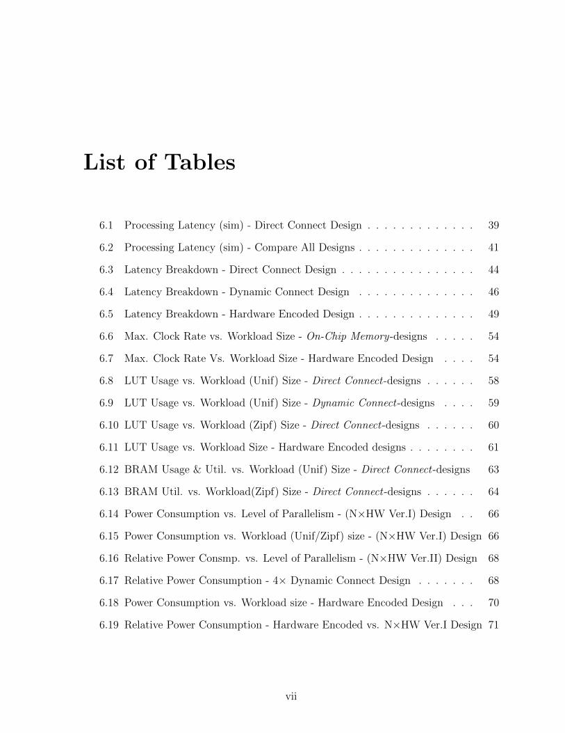
List of Tables
6.1 Processing Latency (sim) - Direct Connect Design . . . . . . . . . . . . . 39
6.2 Processing Latency (sim) - Compare All Designs . . . . . . . . . . . . . . 41
6.3 Latency Breakdown - Direct Connect Design . . . . . . . . . . . . . . . . 44
6.4 Latency Breakdown - Dynamic Connect Design . . . . . . . . . . . . . . 46
6.5 Latency Breakdown - Hardware Encoded Design . . . . . . . . . . . . . . 49
6.6 Max. Clock Rate vs. Workload Size - On-Chip Memory-designs . . . . . 54
6.7 Max. Clock Rate Vs. Workload Size - Hardware Encoded Design . . . . 54
6.8 LUT Usage vs. Workload (Unif) Size - Direct Connect-designs . . . . . . 58
6.9 LUT Usage vs. Workload (Unif) Size - Dynamic Connect-designs . . . . 59
6.10 LUT Usage vs. Workload (Zipf) Size - Direct Connect-designs . . . . . . 60
6.11 LUT Usage vs. Workload Size - Hardware Encoded designs . . . . . . . . 61
6.12 BRAM Usage & Util. vs. Workload (Unif) Size - Direct Connect-designs 63
6.13 BRAM Util. vs. Workload(Zipf) Size - Direct Connect-designs . . . . . . 64
6.14 Power Consumption vs. Level of Parallelism - (N×HW Ver.I) Design . . 66
6.15 Power Consumption vs. Workload (Unif/Zipf) size - (N×HW Ver.I) Design 66
6.16 Relative Power Consmp. vs. Level of Parallelism - (N×HW Ver.II) Design 68
6.17 Relative Power Consumption - 4× Dynamic Connect Design . . . . . . . 68
6.18 Power Consumption vs. Workload size - Hardware Encoded Design . . . 70
6.19 Relative Power Consumption - Hardware Encoded vs. N×HW Ver.I Design 71
vii
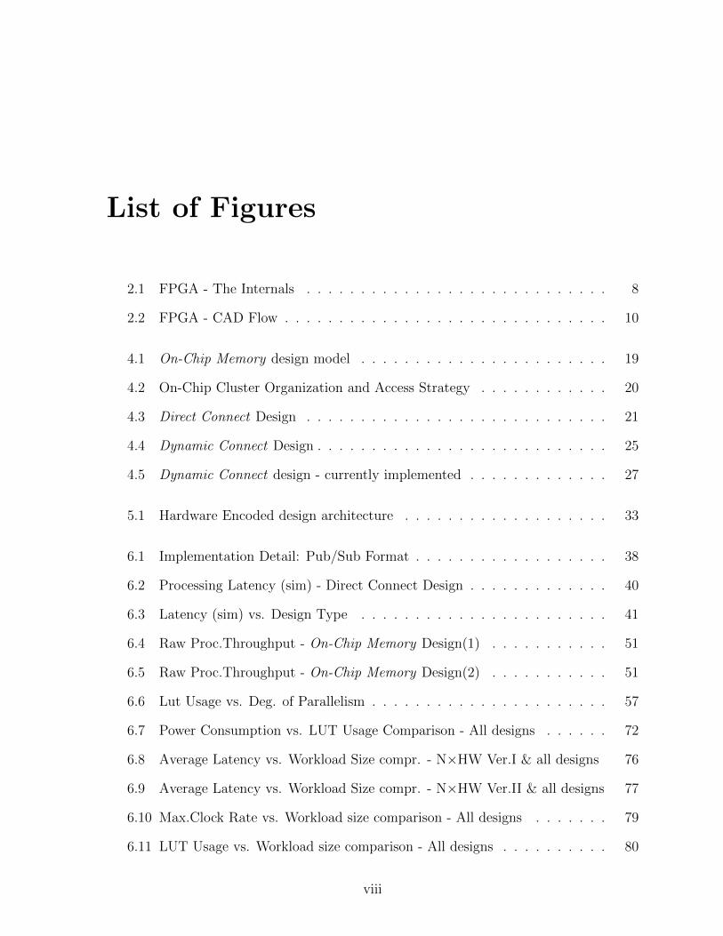
List of Figures
2.1 FPGA - The Internals . . . . . . . . . . . . . . . . . . . . . . . . . . . . 8
2.2 FPGA - CAD Flow . . . . . . . . . . . . . . . . . . . . . . . . . . . . . . 10
4.1 On-Chip Memory design model . . . . . . . . . . . . . . . . . . . . . . . 19
4.2 On-Chip Cluster Organization and Access Strategy . . . . . . . . . . . . 20
4.3 Direct Connect Design . . . . . . . . . . . . . . . . . . . . . . . . . . . . 21
4.4 Dynamic Connect Design . . . . . . . . . . . . . . . . . . . . . . . . . . . 25
4.5 Dynamic Connect design - currently implemented . . . . . . . . . . . . . 27
5.1 Hardware Encoded design architecture . . . . . . . . . . . . . . . . . . . 33
6.1 Implementation Detail: Pub/Sub Format . . . . . . . . . . . . . . . . . . 38
6.2 Processing Latency (sim) - Direct Connect Design . . . . . . . . . . . . . 40
6.3 Latency (sim) vs. Design Type . . . . . . . . . . . . . . . . . . . . . . . 41
6.4 Raw Proc.Throughput - On-Chip Memory Design(1) . . . . . . . . . . . 51
6.5 Raw Proc.Throughput - On-Chip Memory Design(2) . . . . . . . . . . . 51
6.6 Lut Usage vs. Deg. of Parallelism . . . . . . . . . . . . . . . . . . . . . . 57
6.7 Power Consumption vs. LUT Usage Comparison - All designs . . . . . . 72
6.8 Average Latency vs. Workload Size compr. - N×HW Ver.I & all designs 76
6.9 Average Latency vs. Workload Size compr. - N×HW Ver.II & all designs 77
6.10 Max.Clock Rate vs. Workload size comparison - All designs . . . . . . . 79
6.11 LUT Usage vs. Workload size comparison - All designs . . . . . . . . . . 80
viii

6.12 BRAM Util. vs. Wrk.load(unif) size vs. parallelism - Direct Connect designs 82
6.13 BRAM Util. vs. Wrk.load(zipf) size vs. parallelism - Direct Connect designs 83
6.14 Raw Processing Throughput vs. Line Rate . . . . . . . . . . . . . . . . . 85
6.15 Event Processing Throughput vs. Line Rate . . . . . . . . . . . . . . . . 87
A.1 4×VbMc . . . . . . . . . . . . . . . . . . . . . . . . . . . . . . . . . . . . 90
A.2 Cross-Bar Design . . . . . . . . . . . . . . . . . . . . . . . . . . . . . . . 92
A.3 VbMc & Xbar Control Table . . . . . . . . . . . . . . . . . . . . . . . . . 93
A.4 Preliminary Results for 4× Dynamic Connect Design . . . . . . . . . . . 94
ix

Chapter 1
Introduction
1.1 Motivation
The next generation of line-rate1 middleware is becoming an integral part of a growing
number of event processing applications such as real-time data analytics [27, 4, 33],
intrusion detection [4, 7], algorithmic trading [24], targeted advertisements [14, 8, 23],
and (complex) event processing [1, 6, 5, 3, 31, 8, 22, 23]. What is common among all these
scenarios is a predefined set of patterns (subscriptions) and an unbounded event stream
of incoming data (events) that must be processed against these patterns in real-time over
high-rate data streams.
In particular, the challenges for today’s real-time data analytics platforms are to meet
the ever growing demands in processing large volumes of data at predictably low latencies
across many application scenarios. For example, the volume of traffic on the Internet has
undergone an immense increase over the last decade which is apparent in deployments of
high communication bandwidth links across the globe (e.g., OC192 at 9.92Gbit/s). Fur-
thermore, according to Gilbert’s law, communication bandwidth is projected to double
1The term line-rate processing often refers to the processing throughput required for a network deviceto seamlessly perform data analysis faster than the link data rates in order to avoid adding any delaysto the flow of network traffic.
1
Chapter 1. Introduction 2
every 9 to 10 months, but conventional computation architectures underlying existing
middleware systems are showing signs of saturation in terms of offering the necessary
processing bandwidth to sustain demands imposed by future growth of Internet band-
width.
Achieving high processing bandwidth is the key ingredient in enabling the innovation
of high-throughput real-time data analytics to process, analyze, and extract relevant
information from streams of events. Therefore, as proliferation of data and bandwidth
continues, it is becoming essential to expand the research horizon to go beyond the
conventional software-based approaches and adopt other key enabling technologies such
as reconfigurable hardware in form of FPGAs, for example. A Field Programmable Gate
Array (FPGA) offers a cost-effective hardware acceleration option that has the potential
to excel at analytics-based computations due to their inherent parallelism. FPGAs can
exploit low-level data and functional parallelism in applications with custom, application-
specific circuits that can be re-configured, even after the FPGA has been deployed.
In addition, FPGAs can meet the required elasticity in scaling out to meet increasing
throughput demands of time-critical middleware applications.
However, this revolutionary outlook has a few caveats that make the acceleration of
any data processing with FPGAs a challenging undertaking for our middleware systems
community as a whole. First, current FPGAs (e.g., 800MHz Xilinx Virtex 6) are still
much slower compared to commodity CPUs (e.g., 3.2 GHz Intel Core i7), yet on the
positive side, FGPAs have the potential to utilize faster and greater transistor density
processors in the time to come. Second, the accelerated application functionality has
to be amenable to parallel processing. Third, the on-/off-chip data rates must keep
up with chip processing speeds to realize a processing speedup by keeping the custom-
built processing pipeline busy. Finally, FPGAs restrict the designer’s flexibility and
the application’s dynamism, both of which are hardly a concern in standard software
solutions. However, the true success of FPGAs is rooted in three distinctive features:

Chapter 1. Introduction 3
hardware parallelism, hardware reconfigurability, and substantially higher throughput
rates. Moreover, an FPGA can also be utilized, as an evolutionary outlook, as a non-
intrusive interface that sits between the traditional middleware and the network, to enrich
the functionality of middleware without actually changing the engine. One possible add-
on functionality that we envision is to annotate data packets with lineage and provenance
information as they pass through the middleware; this need for maintaining provenance
information is a well-known challenge [30, 15, 12, 9].
Therefore, we must seek innovate approaches to effectively enable meeting the de-
mands of middleware for data-intensive application through hardware acceleration in the
coming years. On this front, programming on hardware is becoming more accessible to
the software community due to the number of research and industry projects that are
working on adapting a higher-level language (such as Java or C) and runtime environment
that dynamically and adaptively allows (all) portions of an application to be executed
on both software and hardware or on developing software-to-hardware compilers. An
example of the former project is IBM Liquid Metal, that is, based on a Java-compatible
language and a runtime that enables execution on both FPGA and GPU [2, 26]; exam-
ples of the latter initiative for accelerating software algorithms on FPGA are ImpulseC
C-to-FPGA2 and OSCI C++-to-FPGA3.
1.2 Problem Statement
Motivated by the above technological trend towards employing highly specialized hard-
ware for various software applications coupled with the fact that current state-of-the
art is quite lacking in addressing the problem of publish-subscribe matching at line-rate
throughputs - we therefore, endeavour to gather results for the following specific ques-
tions.
2http://www.impulseaccelerated.com/3http://www.systemc.org/
Chapter 1. Introduction 4
1. How fast can we execute publish-subscribe matching on FPGAs?
2. What is the highest level of parallelism that can be achieved?
3. How many subscriptions can be supported?
4. What are the hardware and energy consumption costs involved?
Answers to the above questions will help clarify the feasibility of using FPGAs for
publish-subscribe matching and pave the way for future hardware based designs targeted
for line-rate middleware applications and other event processing systems.
1.3 Contributions
We draw our vision as an FPGA-based middleware supporting line-rate processing of data
streams (events) over a collections of patterns (subscriptions). As a first step towards
line-rate FPGA-based middleware, we make the following contributions.
1. We lay out our vision towards achieving line-rate middleware through reconfigurable
hardware—FPGA (cf. Sec. 2,3.3).
2. We introduce a novel hardware design that focuses on increasing the level of par-
allelism through horizontal data partitioning while leveraging the on-chip memory
with direct memory-to-processor interface (cf. Sec. 4.2).
3. We propose a novel hardware design that minimizes overall chip idleness, adapts as
subscriptions workload changes, and enables subscriptions updates. The key intu-
itions governing this design are flexible and dynamic memory-to-processor interface
to equate the memory and processing bandwidth and de-coupling of memory and
matching units (custom processors) to adapt as subscription workload changes (cf.
Sec. 4.3).
Chapter 1. Introduction 5
4. We develop a novel pure-hardware design (with no on-chip memory) that encodes
the subscriptions directly onto the hardware to reach the maximum level of through-
put (for a static subscription set), i.e, achieving the highest level of parallelism in
our design space, and supports subscriptions consisting of arbitrary Boolean ex-
pression; moreover, its novel encoding reduces resource usage, essentially, gives rise
to an effective compression technique that enables scaling to a large number of
subscriptions (cf. Sec. 5.1).
5. We present a comprehensive evaluation to explore our design space for various
workload statistics and in-depth study of FPGA on-chip resource-usage and energy
consumption (cf. Sec. 6).
Our contributions leverage the ability of an FPGA to be re-configured on-demand
into a custom hardware circuit with a high degree of parallelism, which is the key ad-
vantage over commodity CPUs for data and event processing in middleware. Using a
powerful multi-core CPU system does not necessarily increase processing rate (Amdahl’s
Law) as it increases inter-processor signalling and message passing overhead, often re-
quiring complex concurrency management techniques at the program and OS level. In
contrast, FPGAs allow us to get around these limitations due to their intrinsic highly
inter-connected architecture and the ability to create custom logic on the fly to perform
parallel tasks. In our design, we exploit parallelism, owing to the nature of the matching
algorithm, by creating multiple matching units which work in parallel with multi-giga
bit throughput rates, and we utilize reconfigurability by seamlessly adapting relevant
components as subscriptions evolve. Another benefit of an FPGA-based solution is that
there are multiple high bandwidth (giga-bit) I/O pins that allow these devices to be
inserted into the high data-rate streams without added latency on the outgoing traffic.
In modern server systems, however, there is the additional OS layer latency overhead in
moving data between input and output ports. Finally, PCs suffer from the Von Neumann
bottleneck (i.e., discrepancy of CPU speed and memory bandwidth). Current memory
Chapter 1. Introduction 6
interfaces are significantly slower compared to the rate of data being utilized by the
processors. Hence, until innovations such as optically-coupled-memories and optical in-
terconnect fabric technology become available [10] memory access latency must also be
considered while designing FPGA-based hardware solutions. We also address this issue
in two ways: using our dynamic memory-to-processor interface to balance the process-
ing and memory bandwidth and in our pure-hardware design to completely eliminate
memory and processing bandwidth mismatch.
1.4 Thesis Structure
The remaining chapters of this thesis are organized as follows: Chapter 2 provides the
necessary background about the basic internal components of an FPGA, overview of the
design flow methodology and target applications that are relevant to this work. Chapter 3
summarizes relevant work in the area of fpga-based matching including regular expression
based matching. We also introduce the data processing model, data structure and the
matching algorithm employed for all our hardware based designs, followed by outlining
our hardware design model. We begin the description of our proposed On-chip Memory-
based architecture in Chapter 4 where we also discuss particular trade-offs exhibited by
each of the designs implemented based on this architecture and finally provide a step-
wise description of how the design runs in reality. Above structure is again repeated in
Chapter 5 where we now discuss about our Hardware Encoded Data-based architecture.
In Chapter 6 we evaluate all the designs against various design metrics and measurement
data. Towards the end of this chapter a summary of the results (c.f.Section 6.7) is
included to highlight some of the key findings from the data presented in previous sections
of the chapter. Finally, we conclude our work and outline future research directions in
Chapter 7. Additional implementation details regarding the Dynamic Connect design is
also provided in Appendix A.
Chapter 2
Background
Field Programmable Gate Arrays bring to realization a platform for developers to pro-
totype and implement any system conceivable with ever shorter development time. In
contrast, the predominant Application Specific Integrated Circuit (ASIC) design involves
elaborate design steps and expensive fabrication processes; thus, making it impossible to
customize the ASIC after it is fabricated and shipped to the client. FPGAs are repro-
grammable devices and can be updated in a few seconds to meet the new requirements as
it evolves over time. Currently, FPGAs for designers are increasingly becoming a viable
alternative for accelerating software applications by designing custom accelerators to sur-
gically exploit higher level of parallelism that is inherent in the algorithm but is otherwise
inhibited to achieve even when ran on a high-end commodity multi-core CPU system.
Thus, the key crowning advantages of a FPGA based design are re-programmability,
parallelism and shorter development cycle.
2.1 FPGA - The Internals
FPGAs contain a matrix of interconnected discrete Static RAM cells (cf. Fig. 2.1) which
can realize any boolean function (few vendors utilize FLASH based non-volatile memory
cells for FPGAs that require retaining the configuration while power is switched off).
7

Chapter 2. Background 8
Figure 2.1: Fundamental Internal Components of a FPGA. An example of a 2-input LUT is
shown to implement an XOR gate. An LUT comprises of a memory cell and a
multiplexer to select each of its address location. Each SLICE contains 4 6-input
LUT and a DFF pair each with a by-pass MUX. CLBs are interconnected to
the FPGA Interconnection Matrix via cross-point switches toggled by the design
bitstream.
Each memory cell, called the Look-Up-Table (LUT), is essentially implemented as a 2N
bit array where, N is number of address lines for the LUT. Each LUT is capable of
implementing an N-input, 1-bit output boolean function (circuit) by saving all circuit
output valuations for each N-input combination. Therefore, a LUT is an incarnate of
a truth-table constituting the most fundamental block of the FPGA fabric. A D-type
Flip-Flop (DFF) register selectable via a 2-1 multiplexer, is present at the output of each
LUT to either realize a combinational (asynchronous) circuit by by-passing the DFF or a
sequential circuit by selecting DFF to latch the output result every clock cycle. Lower gate
delay and higher logic density are the two major advantages of a LUT based architecture
compared to that offered by other families of CPLDs (Complex Programmable Logic
Devices), since the gate delay associated with a LUT based N-input combinational circuit

Chapter 2. Background 9
is equal to the latency for a single look-up into the LUT. Next higher level in the hierarchy
of the FPGA internal blocks, is a SLICE1 that contain 4 6-input LUTs, 4 DFFs with
additional routing logic to connect with neighbouring SLICEs. Some SLICE (dedicated
for digital signal processing) DSP, contain discrete multipliers and shift-register blocks.
Moving further up the hierarchy, we encounter a Configurable Logic Block (CLB) that
contains 4 SLICEs with horizontal and vertical routing resources that enable each CLB
to interface with neighbouring CLBs or to by-pass signals unaffected through to other
CLBs. Fast cross-point switches make/break interconnections between CLBs and high
speed IOBs (I/O blocks) with intended signal processors via the on-chip interconnection
matrix. The cross-point switches are individually toggled when the FPGA is configured
by downloading the configuration bitstream containing the final compiled design.
FPGA also offers two on-chip memory options: Block RAM (BRAM) and Distributed
RAM. BRAMs are discrete dual-ported single-cycle access latency on-chip memories that
offer several kilobits of storage. These can either be initialized with data at configuration
time or be internally updated at run time. Block RAM in Xilinx Vertex 5 family of
FPGAs are available as 36Kb×1 discrete blocks but each can be used as two independent
18Kb×1 blocks. Moreover, several BRAM blocks can be tied together to create wide
ported memories, without paying any fan-out penalty. Distributed RAM is realized by
configuring several LUT based cells to act as memory. Distributed RAM is expensive
and is generally discouraged, as it reduces the logic real estate available on the FPGA
and incurs higher signal routing cost.
2.2 FPGA - Design Steps
Design entry usually starts with the description of the digital circuit using a high level
Hardware Description Language (HDL) such as Verilog, VHDL or SystemVerilog (cf.
1SLICE is a Xilinx specific terminology.

Chapter 2. Background 10
Figure 2.2: FPGA CAD Flow
Fig. 2.2). These allow users to specify the circuit behaviourally using traditional C++
style keywords for condition, loop and data type specification. In addition to this HDL
also includes special expressions to express concurrency and timing specific behaviour
between various processes. A more direct form of design description using gate level
constructs is also supported by the HDL. Once the design description has been com-
pleted a synthesis tool is used to convert the circuit description into a netlist file which
contains circuit implementation consisting of gate instances and connections (nets) be-
tween them. A netlist is platform independent and does not include any user specified
timing constraints. Once the netlist has been generated it needs to be customized for
implementation on a specific target technology. This step is called, Design Mapping (cf.
Fig. 2.2) and is carried out by vendor specific tool suites that replace generic netlist
gate instances with appropriate gate instances from a hardware library that meet user
specified timing, energy and device space constraints. Design Mapped output is in vendor
specific circuit format and is targeted to run on a particular FPGA technology.
Finally, a Place & Route (PAR) tool maps the timing critical design components
to the appropriate sections of the FPGA and optimizes on-chip signal routes; both of
these steps significantly impact the over all maximum clock frequency the design can be
safely run at without causing timing violations and other erratic behaviour. Of course
the designer, cognizant of the underlying FPGA architecture, can always vary the initial

Chapter 2. Background 11
design description to take advantage of the special features of the physical hardware and
reduce signal routing cost to potentially speed up the design operation. Generally, signal
routing cost goes up as more nets carrying frequently changing states (especially clocks)
must be routed along longer paths across the chip fabric introducing race conditions and
signal skews. Moreover, the designer may often be forced to trade-off simpler design
complexity utilizing slower wide-width data bus for a high bandwidth serial link utilizing
dedicated SERDES (serializer/deserializer) IP blocks. The final PAR design is compiled
and encoded into a bitstream file that is used to configure the FPGA. Bitstream can
either be downloaded to the FPGA via the JTAG port using the boundary scan protocol
or be stored on an on-board FLASH memory to configure the FPGA every time upon
power-up.
2.3 FPGA - Employed for Acceleration
There are two primary schemes by which FPGAs may be employed to accelerate software
application. First most common scheme is to use a hybrid computing model that uses
heterogeneous computing platforms (e.g., Supercomputer Cray XD1, Intel Stellarton) fea-
turing an array of FPGAs instantiated on the motherboard as additional computational
units along side mainstream multi-core CPUs. These FPGAs can either be programmed
with an application specific accelerator (co-porocessor) design that helps to off-load cer-
tain computation intensive task from the main CPU or may even be programmed with a
standard x86 architecture processors to execute segments of application code in parallel.
The current challenge is with the software application and OS developers to generate
code that is well partitioned to take advantage of these hybrid processing elements in
real-time. FPGAs have high-bandwidth interface pins (IOBs) that enable them to be
seamlessly integrated with the rest of the system using standard digital interface stan-
dards (e.g Ethernet, PCIe, USB, SATA, FSB (Front side bus)). Second scheme, is a

Chapter 2. Background 12
non-conventional computation model that is currently an active area of research, is to
develop dedicated stand-alone hardware system solutions. The challenge associated with
this approach is to come up with a clean-slate architecture for running a specific ap-
plication at extremely high rates. We investigate the latter scheme by proposing two
processing models for achieving line-rate processing of middleware applications.
2.4 Target Application
We choose a real-world middleware application of a content based router (CBR) operating
in the context of automated financial trading environment as the target candidate to
achieve line-rate processing via FPGA-based acceleration. A CBR is an event processing
platform which forwards events (publications) to interested parties (subscribers) based
on whether the subscriber has expressed interest in that event by subscribing to it. This
is an important element of content-based routing.
An example application of a CBR in algorithmic trading, where financial news and
market data are expressed as publications such as: [stock = ABX, TSXask = 40.04,
NYSEask = 40.05]; and investment strategies are formulated by financial institutions and
brokers in the form of subscriptions such as: [stock = ABX, TSXask 6= NYSEask] or
[stock = ABX, TSXask ≤ 40.04]. A scalable CBR operating at line-rate must efficiently
find all investment strategies (subscriptions) that match incoming market events faster
than network rates (1Gb/s), supporting up to a million market events per second [34].
Our proposed dedicated FPGA-based solution achieves (1.06Gb/s) raw processing rates
while processing 8 million (8.33Mmps) events per second throughput 2, without incur-
ring the complexities, resource overheads, memory coherence issues involved in designing
a similar system in software running on a muti-processor system.
2Value quoted for Hardware Encoded design operating at 125Mhz. As shown in Figure 6.15) and6.14
Chapter 3
Related Work
3.1 FPGA
An FPGA is a semiconductor device with programmable lookup-tables (LUTs) that are
used to implement truth tables for logic circuits with a small number of inputs (on the
order of 4 to 6 typically). FPGAs may also contain memory in the form of flip-flops and
block RAMs (BRAMs), which are small memories (a few kilobits), that together provide
small storage capacity but a large bandwidth for circuits in the FPGA. Thousands of
these building blocks are connected with a programmable interconnect to implement
larger-scale circuits.
Past work has shown that FPGAs are a viable solution for building custom accelerated
components [16, 18, 29, 17, 19, 32, 20, 24, 28, 35, 36]. For instance, [16] demonstrates a
design for accelerated XML processing, and [17] shows an FPGA solution for processing
market feed data. As opposed to these approaches, our work concentrates on supporting
a FPGA-based middleware for general event processing applications specifically designed
to accelerate the event matching computation. Similarly, [19] presents a database query
processing framework that uses FPGAs to efficiently run hardware-encoded queries while
in [32], demonstrated running hardware-encoded regular expression queries; the key in-
13

Chapter 3. Related Work 14
sight was the realization that the deterministic finite automata (DFA), although suitable
for software solutions, results in explosion of space; thereby, to bound the required space
on the FPGA, a non-deterministic finite automata (NFA) is utilized in [35], [36]. Our
approach differs from [19, 32] as we primarily focus on developing FPGA-based mid-
dleware (as opposed to running a database query on hardware) for large scale event
processing applications that scales to thousands of subscriptions on a single FPGA chip,
while stacking multiple FPGA chips enables the scaling to millions of subscriptions.
On a different front, a recent body of work has emerged that investigates the use of
new hardware architectures for data management systems [11]; for instance, multi-core
architectures were utilized to improve the performance of database storage manager [13]
and to enhance the transaction and query processing [21].
Finally, the sketch of our initial experience with FPGA-based event processing was
presented in [24, 25]; however, our current work aims to address a boarder vision that
aims at developing a generic FPGA-based middleware solution designed for wide range of
event processing applications. Toward this end, this work introduces two novel categories
of chip designs: (1) the on-chip memory design that with the use of novel memory-
to-processor interface minimizes the chip idleness, which was the main shortcoming in
designs developed in [24, 25], and that by decoupling the memory and matching units
adapts to changes in subscriptions workload, which was also lacked in [24, 25], and (2)
pure-hardware design solution that encodes the subscriptions directly onto the hardware
to reach the maximum level of throughput for subscription workload that are orders of
magnitude larger that those supported in [24, 25], and also supports subscriptions having
arbitrary Boolean expression which again was not supported in [24, 25]. Another major
contribution of this work is an extensive experimental evaluation for various workload
statistics and in-depth study of FPGA on-chip resource-usage and energy and power
consumptions, which were not addressed in the prior work [24, 25].

Chapter 3. Related Work 15
3.2 Matching
The matching is one of the main computation intensive components of event process-
ing which has been well studied over the past decade (e.g., [1, 6, 5, 3, 8, 22, 23]). In
general, the matching algorithms are classified as (1) counting-based [6, 31], and (2) tree-
based [1, 23]. The counting algorithm is based on the observation that subscriptions tend
to share many common predicates; thus, the counting method minimizes the number of
predicate evaluations by constructing an inverted index over all unique predicates. Sim-
ilarly, the tree-based methods are designed to reduce predicate evaluations; in addition,
they recursively cut through space and eliminate subscriptions on the first encounter
with an unsatisfiable predicate. The counting- and tree-based approaches can be further
classified as either key-based (in which for each subscription a set of predicates are chosen
as identifiers [6]), or as non-key method [1]. In general, the key-based methods reduce
memory access, improve memory locality, and increase parallelism, which are essentials
for a hardware implementation. One of the most prominent counting-based matching
algorithms are Propagation [6], a key-based method while one of the most prominent
tree-based approach, BE-Tree, which is also a key-based method [23].
3.3 FPGA-based Middleware Architecture
Data processing and hardware design models are the key cornerstones of our implemented
FPGA-based system as they govern system functionality and performance requirements.
3.3.1 Data Processing Model
Subscription Language & Semantics The matching algorithm takes as input an event
(e.g., market event, stock feed, user profile) and a set of subscriptions (e.g., investment
strategies, targeted advertisement constraints) and returns matching events. The event
is modeled as a value assignment to attributes and the subscription is modeled as a
Chapter 3. Related Work 16
Boolean expression. Each Boolean predicate is a triple, i.e., [attributei, operator, values].
Formally, the matching problem is defined as follows: given an event e and a set of
subscriptions, find all subscriptions si satisfied by e.
Matching Algorithm The Propagation algorithm is a state-of-the-art key-based
counting method that operates as follows [6]. The Propagation data structure has three
main strengths which makes it an ideal candidate for a hardware-based implementation:
(1) subscriptions are distributed into a set of disjoint clusters which enables highly paral-
lelizable event matching through many specialized hardware matching units, (2) within
each cluster, subscriptions are stored as contiguous blocks of memory which enables fast
sequential access and improves memory locality, and (3) the subscriptions are arranged
according to their number of predicates which enables prefetching and reduces memory
accesses and cache misses [6].
3.3.2 Hardware Design Model
A high-level classification of our proposed architectures is best represented by the fol-
lowing two abstract hardware design models: (I) On-chip Memory based design (II)
Hardware Encoded Data design. Each of the two design abstractions offer trade-off be-
tween performance (i.e end-to-end processing time, maximum clock frequency supported
and degree of parallelism exploited) versus system scalability (i.e utilization of hard-
ware resources) for a given subscription workload. In what follows, we provide in-depth
description and analysis of the various FPGA designs that we have proposed.

Chapter 4
On-Chip Memory-based
Architecture Model
In this section we present two novel architecture models which enable creation of designs
that utilize on-chip memory resources to perform Publish/Subscribe matching in a highly
parallelized fashion.
4.1 On-Chip Memory-based Designs
The On-chip Memory-based design abstraction, models the architectures that store sub-
scription workload data on fast (single-cycle access latency) on-chip (BRAM) memories
that are distributed across the FPGA chip (Sec. 2.1). The distributed nature of these
memories lends itself to circumventing the Von-Neumann memory bottleneck by utilizing
dedicated high bandwidth memory-to-processing unit interconnect. Von-Neumann mem-
ory bottleneck is most common in chip-multi-processor architectures, where fast parallel
processing units are coupled with large capacity memories via shared address/data buses,
which ultimately undermine the performance by forcing the processing units to stall for
several clock cycles while data is fetched. Using multiple off-chip (DRAM) memories
via dedicated interfaces is certainly an alternative to match processing bandwidth with
17

Chapter 4. On-Chip Memory-based Architecture Model 18
equal memory bandwidth, however one must be aware of the multi-cycle access latencies
associated with them, which requires the need to use faster on-chip cache or data transfer
buffers. Demand for large capacity memories by typical data centric applications have
usually neglected the potential of utilizing the fast high bandwidth on-chip memories due
to the limited capacities offered by the current state-of-the-art. However, trends predict
on-chip memory capacities to grow much faster than the meager reduction of, already
plateauing, access latencies for off-chip memories. Furthermore, many high speed appli-
cations rely on a very limited and relatively static mission critical data, which is ideal for
a On-chip Memory-based design implementation. Motivated by the above observations
we adopt On-chip Memory design abstraction as our design basis to implement and eval-
uate the Direct Connect (i.e., direct memory-to-processor interface) and the Dynamic
Connect (i.e., dynamic memory-to-processor interface), shown in Fig. 4.1 and Fig. 4.4,
respectively, architectures. These two architectures highlight two distinct approaches of
coupling several parallel processing units with distributed on-chip memories.
Chapter 4. On-Chip Memory-based Architecture Model 19
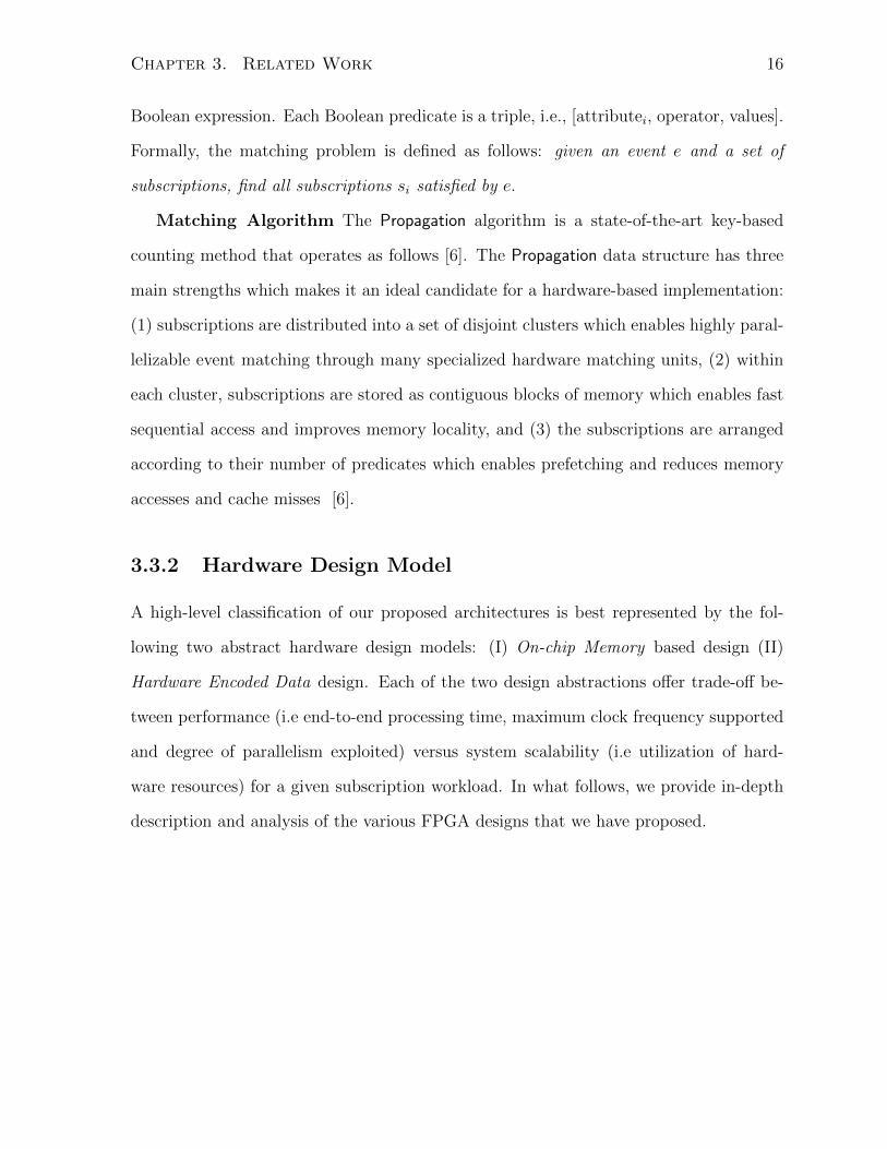
4.2 Direct Connect - Architecture Overview
Figure 4.1: On-Chip Memory design model based Direct Connect architecture. Pro-
cessing bandwidth is wasted due to idling of matching units due
to variation in the distribution of subscription workload data set
across each BRAM table (e.g. at time step t2 and t3 ).
Why use Direct Connect memory model?
Direct Connect architecture (Fig. 4.1) features an On-chip memory-based design in
which every subscription matching unit (MU) is directly coupled with a dedicated BRAM
block (subscription table), thereby allowing every MU to operate in parallel and in-synch
with each other. The are two key benefits for a Direct Connect architecture. First, this
architecture fully utilizes the available distributed on-chip (BRAM) memory resources by
partitioning and uniformly distributing the global Propagation algorithm’s data structure
across each BRAM associated with a matching unit (MU). The Direct Connect then
allows each MU an exclusive access to a chunk of the global Propagation algorithm’s data
structure residing in its dedicated BRAM. Therefore, the degree of parallelism is a direct
function of the degree of horizontal data partitioning (specified as a parameter during
the design synthesis stage) and is limited ultimately by the number of MUs that can
be physically supported by available hardware resources of the underlying FPGA chip.
Secondly, the Direct Connect interface between the MUs and dedicated BRAM units
avoids complicated arbitration and hand-shaking logic that is otherwise required with

Chapter 4. On-Chip Memory-based Architecture Model 20
using shared memory.
Despite, the ease with which the Direct Connect architecture based designs can be
scaled to higher degree of parallelism, they’re quite sensitive to the distribution of work-
load across all the BRAM tables. Therefore, we ensure that each BRAM table contains
an equally sized subset of every subscription cluster. Otherwise, an uneven distribution
of subscription cluster data will cause some MUs to exhaust their data sooner and remain
idle before the rest have completed matching, thus nullifying the overall gain of having
scaled up to the design containing more MUs (higher degree of parallelism) - idling MUs
represent waste of available processing bandwidth. This scenario is depicted in Fig. 4.1,
where at time step t1 all MUs are utilized since each BRAM has sufficient subscription
data. However, at time step t2 BRAM3 and BRAM4 have no more valid data to supply
to MU3 and MU4 respectively, thus causing these to idle which is equivalent to a 50%
reduction in the degree of parallelism.
4.2.1 On-Chip Cluster Access
Figure 4.2: On-Chip Cluster Organization and Access Strategy
A performance limiting component in the On-Chip Memory-based Designs is the
system that controls access to the on-chip subscription data store. Figure 4.2 depicts
the steps involved in order to access/fetch the clusters containing subscriptions that need
to be matched against a given Pub event. Upon arrival of a Pub event (cf. step (1)
in Fig 4.2) containing attribute-value pairs (e.g P1 P2..Pn), each attribute-value pair
is independently hashed to generate a cluster index vector (2) that is used to look-up

Chapter 4. On-Chip Memory-based Architecture Model 21
(3) the cluster address from the Index Table. The cluster Index Table is precomputed
before the design compilation/synthesis is done and stores the physical address of every
cluster that may reside in one or many distributed on-chip memories (cluster distribution
is design dependent). Large size of the index table makes it impractical to duplicate the
table to allow parallel look-up for each cluster index vectors. Therefore, in the current
implementation, access to the Index Table table has been pipelined with the hash function
evaluation step in order to minimize the cluster access serialization latency.
We’ve explored two of several possible schemes of distributing clusters (subscription
data) across multiple on-chip BRAM memory tables. The Direct Connect designs use
even distribution of each cluster across all BRAM memory tables and padding memory
tables with null subscription in case when cluster size (number of subscriptions) is not
completely divisible by the number of memory tables. On the other-hand Dynamic
Connect design allocate each cluster in one BRAM memory table entirely (cluster data
is not distributed).
4.2.2 Direct Connect - Step-wise Operation
Figure 4.3: Currently Implemented Direct Connect design. The step-wise opera-
tion of design is marked by indexed circles.

Chapter 4. On-Chip Memory-based Architecture Model 22
A high-level description of the stepwise operation of our Direct Connect architecture
is depicted in Fig. 4.3. Upon arrival of an event as an UDP packet, the Ethernet controller
and packet parser module (EMAC ) stripes and transfers (1) the packet payload (event) to
the input queue of the system. A custom hardware sub-module, Dispatcher unit, extracts
event attribute-value pairs as input to hash functions for generating cluster indexes (cf.
Section 4.2.1 for description of cluster address look-up steps). Cluster indexes are used to
look-up BRAM cluster start addresses (2) of the relevant subscription clusters residing
in each BRAMs. The Dispatcher then inserts all cluster start addresses (3) into the
cluster address queue, while pops one cluster start address to be fed (4) to all BRAM-
based matching units (BMUs) via the MU Data Bus (common to all BMUs). Next,
all parallel BMUs are signalled to initiate matching (5). Every BMU consists of a four
state Finite State Machine (FSM), that performs matching by sequentially fetching one
subscriptions every clock cycle from the dedicated BRAM memory. Since all BMUs are
run in parallel and in sync with each other, the Dispatcher must dispense (4) the next
cluster start address only when all BMUs have completed matching all subscriptions in
the current cluster. The BMUs stop once they receive a cluster end marker from each
BRAMs. In the final phase (6), once all BMUs finish matching the subscriptions’ in
every cluster accessed by each attribute-value pair of the event, the final result tallying
phase is initiated. In this phase the match results (6) (subscriptions or number of match
found) are placed on the match hit vector and consolidated as a final result value by the
Dispatcher unit followed by inserting it into the result output queue. The final result (7)
is then transferred to the EMAC via the output queue. Lastly, the EMAC assembles
and transmits the UDP result packet to the intended host(s).
4.2.3 Direct Connect - Design Trade-offs
The Good.
The Direct Connect architecture benefits from its embarrassingly parallel and simple

Chapter 4. On-Chip Memory-based Architecture Model 23
design that supports up to hundreds of matching units by horizontally partitioning the
data. This high level parallelism directly translates to boosting system performance;
thus, making it a competitive solution.
The bad and the ugly. There are two performance limiting concerns (besides the
obvious available hardware resource constraint), that emerge as a trade off for the high
degree of parallelism that is offered by the Direct Connect architecture. Namely, first the
performance of the design (Fig. 4.1) is quite sensitive to the distribution of subscription
data across dedicated BRAM for a particular BMU. Secondly, in order to realize a high
degree of parallelism while keeping the system complexity low, all BMUs are operated
in parallel and in sync with each other (lack of pipelining) which translates in all events
being processed sequentially at high rates.
Furthermore, the process of aggregating match results from all BMUs turns out to be
a bottleneck. As all the BMUs must be stalled for the result tallying phase to complete,
which otherwise cannot commence earlier and/or operate in a progressive fashion owing
to the consequences of the first reason (as all BMUs must complete the event matching
phase before results can be tallied.) Therefore, to maximize event processing throughputs
via increase in parallelism in Direct Connect architecture, the subscription data clusters
are required to be distributed evenly across each BMU. The later requirement is also
made clear via an example shown in Fig. 4.1, where at time step t1 all BRAMs are
able to supply data to each MU. However, at time steps t2 and t3 due to change in
subscription distribution in BRAM3 and BRAM4, they are not able to supply MU3 and
MU4 any more data. This causes the matching units to idle thus resulting in wasted
processing bandwidth and lowering the level of parallelism.
Moreover, in consideration of adding the future support of begin able to update
subscription workload during run-time, the Direct Connect architecture offers a trade-off
between the adjustable level of parallelism versus the cost of supporting updates to the
subscription workload at run-time. Therefore, due to the even distribution of global data

Chapter 4. On-Chip Memory-based Architecture Model 24
structure across all BRAMs, it necessitates updating the entire system (all BRAMs)
even if the update concerns a small data set local to a single BRAM. If the system
update is done in parallel (updating all BRAMs concurrently), then the cost entails
added hardware cost of dedicated data/address buses for each BRAM, but if the update
is done sequentially via shared address/data buses, then the cost entails a slower update
cycle and added hardware cost of additional address decode logic for each BRAM. (Note
- current scope of evaluation does not cover subscription update trade-off as mentioned
above.)
Lastly, another trade-off is the even distribution of global data structure across all
BRAMs in the Direct Connect architecture does not bode well for efficient utilization of
on-chip memory space due to the required padding of the cluster data with null subscrip-
tions, done to preserve constant address offsets for each cluster segment stored in every
BRAM table - i.e. the cluster occupancy (size) in all BRAM tables is kept constant such
that all cluster segments begin at the same address in every BRAM table.
4.3 Dynamic Connect - Architecture Overview
Why use Dynamic Connect memory model?
Design level abstraction that formed the seed for the initial concept of an architecture
that guarantees best effort to maximally utilize processing bandwidth, represented by
number of matching units in the system against the available memory output bandwidth,
represented by amount of valid data retrieved by a memory unit per cycle. In the previous
Direct Connect design (cf. Fig. 4.1) each BMU is coupled directly to a dedicated cluster
BRAM unit containing a subset of subscriptions from every cluster. Even, though this is
a highly parallel model for matching, it renders a couple of matching units useless once
the dedicated BRAMs have exhausted the data to supply from a given cluster, i.e., all
MUs must wait until a cluster is completely processed (serializing cluster processing).

Chapter 4. On-Chip Memory-based Architecture Model 25
Figure 4.4: On-Chip Memory design model based Dynamic Connect design. Each MU
is decoupled from the BRAM units. The cross-bar based intercon-
nect dynamically matches available memory bandwidth with process-
ing bandwidth. At time step t1 all VbMc are requested to output
1 (1x bandwidth) subscription per cycle. However, at time step t2
VbMc1 and VbMc2 are requested to operate at 2x bandwidth and
the cross-bar routes additional two subscriptions to MU3 and MU4,
there by keeping all MUs supplied with data.
In contrast, the Dynamic Connect architecture (cf. Fig. 4.4) decouples the BRAM
units from each MUs via a dedicated ((M×P) inputs to 1 output) cross-bar (Xbar) switch
based interconnect (shown combined as a monolithic Xbar unit in Fig. 4.4). The Xbar
allows dynamic routing of subscription data by dynamically connecting any memory out-
put port from any memory to a matching unit (MU). Moreover, each BRAM is replaced
by a Variable bandwidth Memory controller (VbMc) unit which is a custom wrapper
design built around a conventional BRAM to realize a multi-ported memory with tun-
able output burst length (set by the Bandwidth Request BWr input) during the runtime
(cf. Appendix A for further design details). The VbMc is used to store clusters in their
entirety (i.e. subscription distribution no longer needs to be consistent across multiple
BRAMs in the system) which lends itself to each cluster being processed independently

Chapter 4. On-Chip Memory-based Architecture Model 26
in parallel with other clusters, which is limited only by the processing bandwidth or the
number of matching units available in the system. Even in the worst case, if all clusters
that need to be processed happen to be stored on one VbMc (or BRAM unit), the under-
lying Xbar interconnect is capable of supplying all MUs with subscription data from the
one VbMc unit that is signaled to operate at maximum output bandwidth (i.e. VbMc
BWr input is set to 4×) in Fig. 4.4 to output a new subscription on each of its 4 output
ports every clock cycle. Hence, each cluster is accessed sequentially but always processed
in parallel; thus, none of the MUs are left to idle.
In Fig. 4.4, dynamic routing is exemplified in contrast to the operation seen in the
Direct Connect architecture (cf. Fig. 4.1). At time step t1 all VbMc are operated to
output one subscription per cycle (1× BWr) as each has sufficient data. However, at
time step t2 when VbMc3 and VbMc4 run out of subscription data, in order to avoid
idling of MU3 and MU4, the VbMc1 and VbMc2 are requested to read 2 subscriptions
per cycle (2× BWr) which results in subscription# 3 being routed to MU3 and MU4
via the Xbar - thus the memory output bandwidth is scaled-up to match the processing
bandwidth in-order to compensate for the change in workload distribution.
4.3.1 Dynamic Connect - Step-wise Operation
A high-level description of the stepwise operation of our Dynamic Connect architecture is
depicted in Fig. 4.5. Upon arrival of an event as an UDP packet, the Ethernet controller
and packet parser module (EMAC ) transfers (1) the packet payload (event) into the
input queue. Appropriate cluster start address is found and loaded (2) into the VbMc
units containing those clusters (cf. Section 4.2.1 for description of cluster address look-
up steps). Initially each VbMc starts at 1× bandwidth setting and all cross-bar connect
all MUs to the first port of each VbMc. On subsequent cycles the VbMc BW Controller,
the design runs under the feed-back control loop. The control loop begins with VbMc and
Xbar Controller sampling (3) the bandwidth values (BWavl) currently begin reported
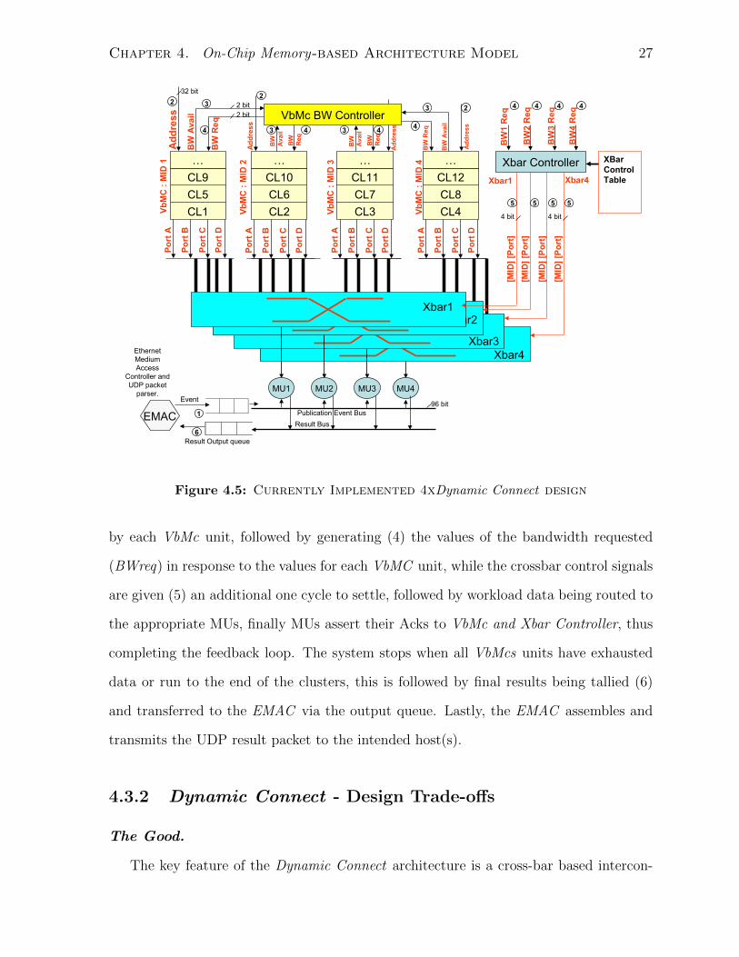
Chapter 4. On-Chip Memory-based Architecture Model 27
Figure 4.5: Currently Implemented 4xDynamic Connect design
by each VbMc unit, followed by generating (4) the values of the bandwidth requested
(BWreq) in response to the values for each VbMC unit, while the crossbar control signals
are given (5) an additional one cycle to settle, followed by workload data being routed to
the appropriate MUs, finally MUs assert their Acks to VbMc and Xbar Controller, thus
completing the feedback loop. The system stops when all VbMcs units have exhausted
data or run to the end of the clusters, this is followed by final results being tallied (6)
and transferred to the EMAC via the output queue. Lastly, the EMAC assembles and
transmits the UDP result packet to the intended host(s).
4.3.2 Dynamic Connect - Design Trade-offs
The Good.
The key feature of the Dynamic Connect architecture is a cross-bar based intercon-
Chapter 4. On-Chip Memory-based Architecture Model 28
nection scheme between the on-chip subscription (workload) data stores (Block RAMs)
and the MUs (matching units) while supporting dynamic distribution of workload across
all the MUs, to keep them evenly supplied with data (with best effort).
As a result the degree of parallelism is retained by dynamically matching the avail-
able processing bandwidth (MUs) against the available memory output bandwidth every
clock cycle; thereby, achieving much finer grained parallelism compared to Direct Con-
nect architecture. Furthermore, Dynamic Connect architecture makes the design least
sensitive to the distribution of workload across the on-chip memories.
In addition, as cluster access adds to the overall processing latency, Dynamic Connect
design attempts to minimize this overhead by: (1) storing each cluster on a on-chip
BRAM memory entirely as opposed to distributing its data over multiple BRAMs. This
allows each MU to access subscriptions from a cluster independently and simultaneously
of other MUs as soon as the cluster address is obtained. In contrast, if a single cluster is
distributed across multiple BRAMs (as is in the case of Direct Connect designs), then all
BRAM memory tables will be busy serving subscription from a cluster to all MUs at a
time while other MUs have to wait for the BRAMs to free up before the next cluster can
be accessed - serializing cluster access. (2) by decoupling the BRAM memory tables from
the MUs, allows easy swapping of BRAM clusters that have been processed completely
with other BRAM clusters that are yet to be processed. Moreover, cluster data in BRAM
does not need to be padded with null subscriptions as each VbMc (BRAM) stores the
cluster in its entirety, resulting in a greater efficiency of on-chip memory usage in contrast
to what is possible in the Direct Connect architecture. The outcome of adopting the
crossbar based interconnect (cf. Fig. 4.4) is the natural realization of the above two
desirable features.
Lastly, aggregation of final match results from all matching units is no longer a bot-
tleneck since it can easily be pipelined to run in a progressive fashion as each matching
unit is sequentially stalled to extract accumulated results while other matching units

Chapter 4. On-Chip Memory-based Architecture Model 29
continue to run, in contrast with Direct Connect architecture, where all BMUs must be
run in synch and cannot not be stalled independently.
The bad and the ugly. The advantages of the Dynamic Connect architecture comes
at the expense of increased design complexity and higher hardware resource utilization
owing to the additional logic required to implement the cross-bar switch, Variable band-
width Memory controller (VbMC ) and cross-bar/VbMc feed-back loop controller. This
design is also more expensive to scale up to support more matching units in comparison to
Direct Connect architecture as a result of the exponential increase in size of the cross-bar
control table with respect to the number of matching units in the design. Therefore, loss
in performance of the Dynamic Connect architecture is attributed to the added latency
incurred as a result of the inter-module synchronization penalty paid along the BWreq
feedback control loop.

Chapter 5
Hardware Encoded Data-based
Architecture Model
In this section we present a novel architecture model that encodes subscription data in
FPGA fabric as circuits to achieve unprecedented level of parallelism while performing
Publish/Subscribe matching.
5.1 Hardware Encoded Data design
The Hardware Encoded Data based design model features an architecture that directly
encodes subscription data into the FPGA fabric as combinational circuits. This design is
a purely hardware solution and attains the highest degree of parallelism possible on the
FPGA platform to match all subscriptions concurrently in one clock cycle. Nevertheless,
at the core of this data processing model lies few key challenges such as finding efficient
data encoders and fast compression and decompression techniques that are ideal for
hardware implementation and finding the optimal encoding scheme that achieves highest
spatial efficiency which ultimately impacts signal routing costs, system operating fre-
quency, and power consumption of the FPGA platform. Towards this end, we implement
and evaluate the Index Encoded architecture, that utilizes bit vector index based encod-
30
Chapter 5. Hardware Encoded Data-based Architecture Model 31
ing to maximize the number of subscriptions that can be supported at a time which also
paves the way for supporting subscriptions defined over arbitrary Boolean expressions.
5.2 Index Encoded - Architecture Overview
The Index Encoded architecture (cf. Fig. 5.1) is built by a compiler that takes as input
a subscription workload and generates two HDL modules: Predicate Detector Array and
Hardware Encoded Sub Array. The Predicate Detector module is generated by first, cre-
ating an index hash map of all unique predicates (attribute, value and operator) found
across subscriptions in the workload. The predicate hash map assigns each predicate a
unique index value ranging from 0 · · ·P − 1 where P is the total number of unique pred-
icates discovered by the compiler. Next, the compiler instantiates Predicate Evaluator
(PE) module to detect and evaluate each predicate inserted into the hash map. Output
of each PE module indicates whether a particular predicate is satisfied by the attribute
and value pairs present in the event. Finally, the outputs of each PE module is latched
by corresponding 1-bit registers whose outputs drive the Pi bit to Predicate Evaluation
(PEVAL) vector. Each bit index of the PEVAL bit vector corresponds to index in the
hash map that is associated with a particular predicate detected and evaluated by a
PE module. Encoding of the actual subscription workload is captured in the Hardware
Encoded Sub. Array module. In order to generate this module, the compiler generates
HDL code for the combinatoric logic that represents the logical relation between the
predicates of each subscription; this logical relation can be of any arbitrary Boolean ex-
pression. Next, the compiler replaces each predicate reference with the corresponding bit
value indexed into the PEVAL bit vector. Therefore, the final index encoded subscription
is essentially a combinatorial circuit, in which each of its inputs represents a predicate
evaluation bit value, and the output represents the result of subscription logic evaluation.

Chapter 5. Hardware Encoded Data-based Architecture Model 32
5.2.1 Index Encoded - Design Trade-offs
Line-rate processing is the prominent advantage of the Hardware Encoded Data-based
design through its embarrassingly parallel structure for static subscription set. The
Index Encoded architecture takes advantage of the fact that there are a relatively small
set of distinct predicates that constitute all subscriptions due the overlap among the
subscription set. Therefore, evaluating all the predicates from this finite set prior to
subscription evaluation avoids having to duplicate hardware resources for re-evaluating
the predicates for each subscription multiple times.

Chapter 5. Hardware Encoded Data-based Architecture Model 33
Figure 5.1: Hardware Encoded design based on Index Encoded architecture. The
step-wise operation of design is marked by indexed circles.
5.2.2 Index Encoded - Step-wise Operation
The Index Encoded architecture operates in two stages (Fig.5.1). In the predicate eval-
uation stage, upon the arrival of an event (1), each of its attribute value pairs (each
demultiplexed on separate lines by the Event Splitter) are sequentially fed via input mul-
tiplexers to the Predicate Evaluator (PE) modules for predicate evaluation. Once all
attribute value pairs have been selected, the outputs of PE in the Predicate Detector
Array are latched (3) to stabilize the value of the PEVAL bit vector that is then fed (4)
to an array of circuits in the subsequent subscription evaluation stages of the operation.

Chapter 5. Hardware Encoded Data-based Architecture Model 34
In the second stage (4), all subscriptions that have been hard-wired to appropriate bits
of the PEVAL bit vector is used to generate an output flag bit from each subscription
circuit. As shown in Fig.5.1 the output of each subscription is OR’d with the output of
the next subscription, this is done in order to carry forward the match results to eliminate
the expensive hardware cost of having to OR all the circuit outputs to generate the final
result. Entire second stage consumes one clock cycle for all the subscription circuit to
set their match result bit. The match results are then tallied pushed (5) into the output
queue for the Ethernet controller module (EMAC) to assemble the UDP result packet to
be sent to the intended host(s).
Chapter 6
Evaluation
In our evaluation, we present the comparison of various aspects of our proposed archi-
tectures built around the On-chip Memory- and Hardware Encoded Data-based design
models. We study these architectures in depth to highlight the relative merits and trade-
offs offered by each of these design models. Furthermore, we envision the two design
models to serve as aids for the system designers to predict the hardware cost and perfor-
mance gains while implementing custom hardware solutions for accelerating middleware
applications using FPGAs.
6.1 Evaluation Methodology
6.1.1 Evaluation Tool and Methodology
Design verification is done using the Modelsim SE 6.6b, a HDL circuit simulator tool
for performing pre-synthesis behavioural simulations and verification of the design logic.
Processing latency in terms of number of clock cycles spent while processing a publica-
tion event by a design under test is initially obtained via behavioural simulations using
Modelsim SE 6.6b. In simulation latency measure entails pushing 5 publication events
back-to-back into the design Input Queue followed by measuring the number of clock
35

Chapter 6. Evaluation 36
cycles spent until a result is pushed into the Output Queue by the design (marking the
end of matching). The measured latency value set is then averaged to obtain a simulated
average latency value for the design. In addition, our actual throughput measurement
testbed involves a host PC running a custom script that transmits a given input stream
of publication event packets over a dedicated gigabit Ethernet link to the target FPGA
board that has been configured with the design under test. Each hardware design incor-
porates a free running count of the number of clock cycles elapsed from when each event
is pushed into the Input Queue till the corresponding result is pushed into the Output
Queue. Cycle count latency value is then sent back as part of the reply packet payload
along with match result from the design after having processed an event. The script on
the host PC stores the reply payload data in an output file for further analysis. Finally,
by averaging the clock cycles spent processing each event, an average end-to-end event
processing latency and event processing throughput for the architecture design under
test is obtained. A Xilinx XPower Analyzer software tool is used to estimate the power
consumption of each post-implemented place and routed designs. This tool is quite ver-
satile in calculating both the Quiescent (static) and Dynamic power consumption values
broken down by design hierarchy. Unlike estimating static power or stand-by power con-
sumption, which depends on the number of transistors in the design, dynamic power
estimate can only be as accurate as the activity (switching) rate information for each
net or signal in the design. For the purpose of our evaluation we use XPower Analyzer’s
default (50% toggle probability per-clock cycle) activity rates for each control and data
net. We understand that the power consumption estimate values thus obtained will be
overly conservative nevertheless these are useful in relative comparison of various de-
signs. Lastly, for occasional instances where on-chip debugging was required, Xilinx’s
ChipScope Analyzer tool was utilized.

Chapter 6. Evaluation 37
6.1.2 Evaluation Platform
Each architecture design is evaluated on a Xilinx ML505 Vertex 5 FPGA evaluation
board featuring one Xilinx Vertex 5 (XC5VLX50T) FPGA chip, 1GigE port and an on-
board 200Mhz clock source. Xilinx Vertex 5 FPGA (XC5VLX50T) device is capable of
operating at 550Mhz and contains four 1Gb/s hardened Ethernet Media Access Controller
IP blocks (only one of which is wired to a physical RJ-45 Ethernet port on the ML505
board), 120× 18Kb BRAM cells (on-chip memory) and 28800 6-input Look-Up-Tables
(LUTs) each with a D flip-flop register.
6.1.3 Workload Description
We compare various designs with key controlled experimental conditions: workload dis-
tribution and workload size. Each subscription (a Boolean expression) in our workload
consists of a set of Boolean predicates, where each predicate is a presented by an at-
tribute, operator, and values. For each workload distribution (Unif - Uniform or Zipf -
Zipfian), predicate’s attribute is chosen based on either a uniform or a Zipfian distribu-
tion; while the predicates operator could be chosen from any common relational operator
such as (<,≤,=,≥, >) and the value is of type integer. On the other hand, for the event
workload, each event is an attribute and value pair, in which the attribute and values
are selected using the same technique as in subscription generation. For example, when
generating the uniform workload, both subscription and event workloads, the attribute
are chosen uniformly from a set of attributes. Finally, on average we use five predicates
per subscriptions and five attribute value pairs for events.
For the purpose of implementation an 8 bit integer value is used to represent each
attribute and value token (restricted between 1 to 10) used in all publication events and
subscriptions, while the pub/sub ID is represented by an 16 bits value. The operator is
always assumed to be equality (=) and therefore is eliminated from the subscription data
Chapter 6. Evaluation 38
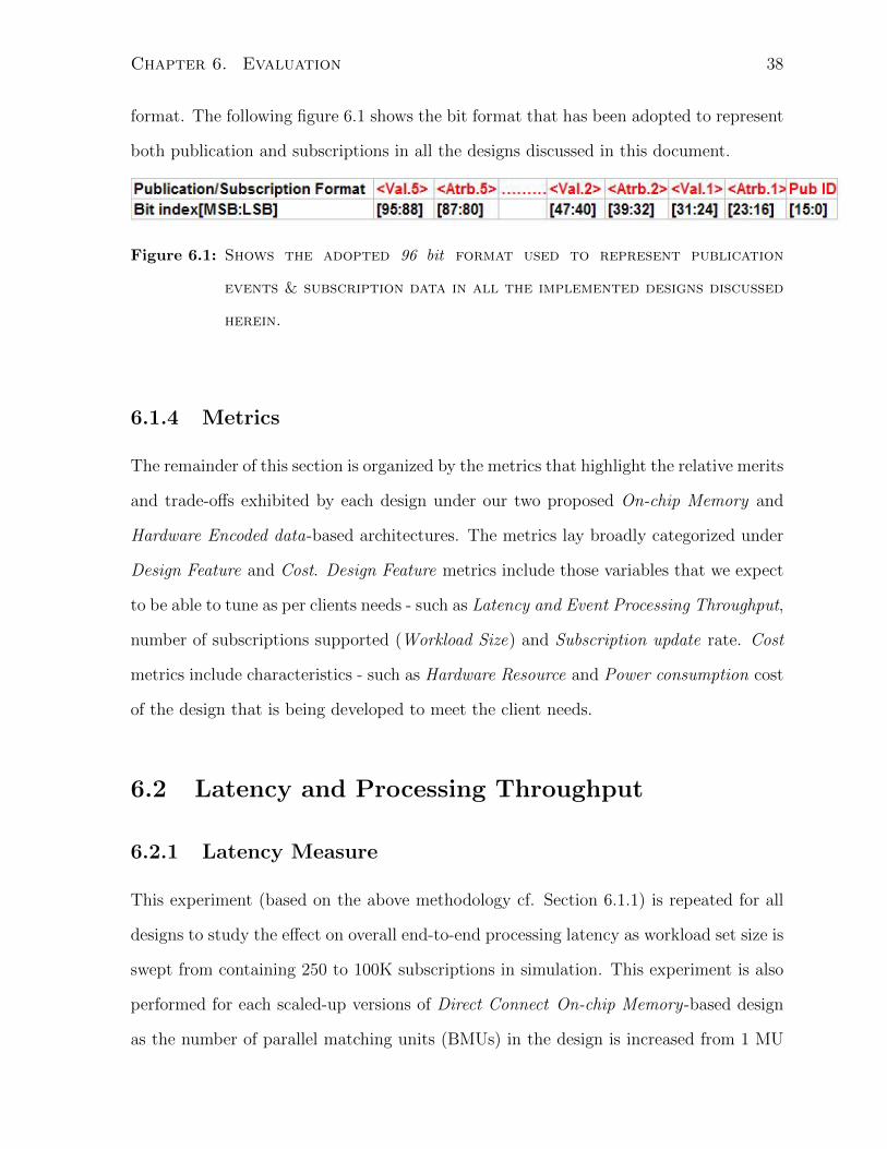
format. The following figure 6.1 shows the bit format that has been adopted to represent
both publication and subscriptions in all the designs discussed in this document.
Figure 6.1: Shows the adopted 96 bit format used to represent publication
events & subscription data in all the implemented designs discussed
herein.
6.1.4 Metrics
The remainder of this section is organized by the metrics that highlight the relative merits
and trade-offs exhibited by each design under our two proposed On-chip Memory and
Hardware Encoded data-based architectures. The metrics lay broadly categorized under
Design Feature and Cost. Design Feature metrics include those variables that we expect
to be able to tune as per clients needs - such as Latency and Event Processing Throughput,
number of subscriptions supported (Workload Size) and Subscription update rate. Cost
metrics include characteristics - such as Hardware Resource and Power consumption cost
of the design that is being developed to meet the client needs.
6.2 Latency and Processing Throughput
6.2.1 Latency Measure
This experiment (based on the above methodology cf. Section 6.1.1) is repeated for all
designs to study the effect on overall end-to-end processing latency as workload set size is
swept from containing 250 to 100K subscriptions in simulation. This experiment is also
performed for each scaled-up versions of Direct Connect On-chip Memory-based design
as the number of parallel matching units (BMUs) in the design is increased from 1 MU

Chapter 6. Evaluation 39
1× MU 4× MUs 32× MUs 128× MUs
250 75 55 50 36
1K 93 61 43 43
10K 640 190 68 54
50K 2235 599 123 73
100K 7146 1826 276 193
Table 6.1: Simulation Results: Processing Latency (# clock cycles) vs. Work-
load size, when # of MUs are swept in the Direct Connect architecture
for On-chip Memory-based design.
(1× parallelism) to 128 MUs (128× parallelism). Finally, each design is synthesized to
generate an implementation bit stream that can be used to program the FPGA evaluation
platform. Processing latency and throughput are also measured in reality by running each
design on the board. In this experiment a stream of fixed size (96 bit) publications is sent
from a host PC (using 64 Byte UDP frame per event) to the FPGA evaluation platform
over a 1 Gbps Ethernet link. In response to each publication event the design replies
back with publication event ID, match result and number of cycles spent matching the
event. Finally, based on all the event replies logged by the host PC, match clock cycle
count values are averaged over number of publication events sent. Actual processing
latency and throughput are easily derived by using operating clock frequency of the
design, network data rate and event packet size.
It is evident from Table 6.1 (cf. Fig. 6.2) that the end-to-end processing latency for the
Direct Connect architecture is improved as we increase the degree of parallelism; in fact,
the improvement is proportional to the number of matching units employed in the design.
For instance, at 250 subscription workload, we only see a 2× improvement in the latency
when scaling from 1× to 128×MUs, whereas for 50K workload, we observe approximately
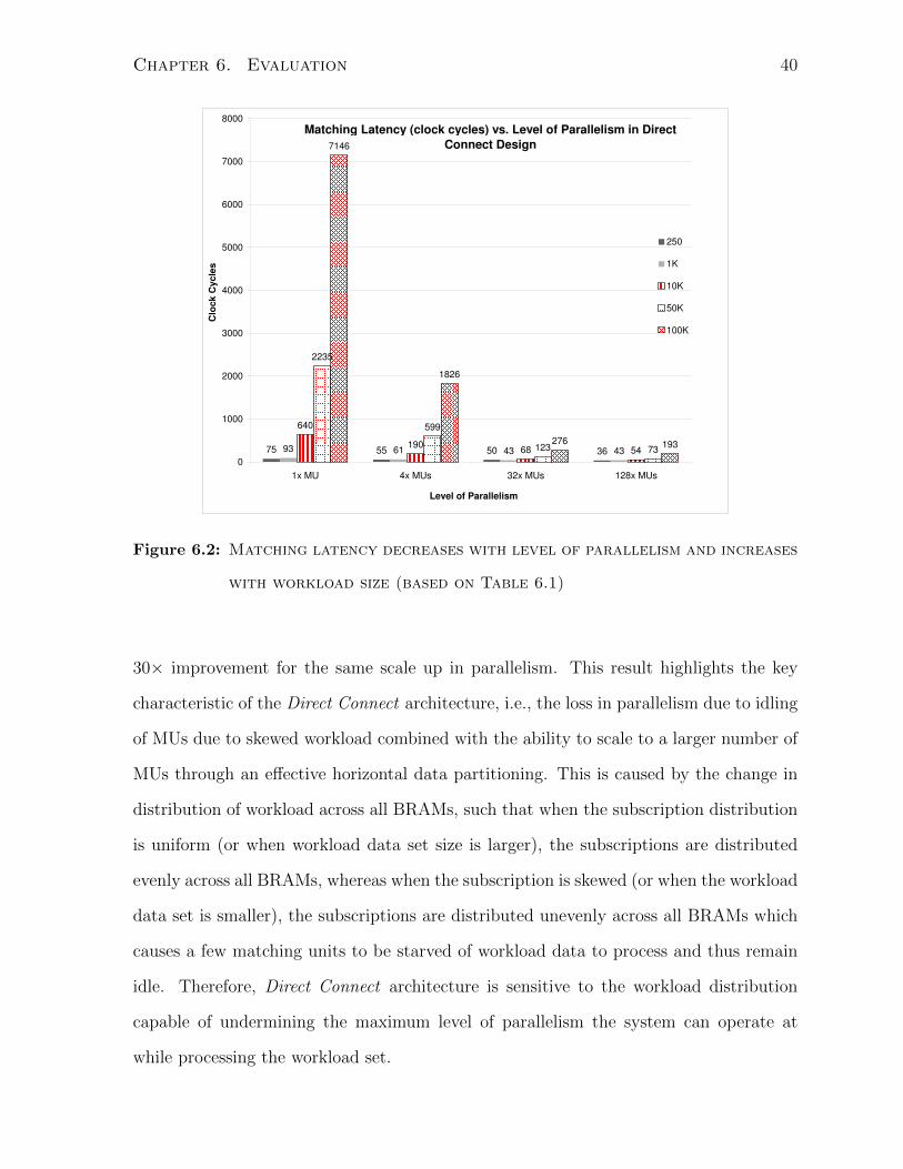
Chapter 6. Evaluation 40
Matching Latency (clock cycles) vs. Level of Parallelism in Direct
Connect Design
75 55 50 3693 61 43 43
640
19068 54
2235
599
123 73
7146
1826
276193
0
1000
2000
3000
4000
5000
6000
7000
8000
1x MU 4x MUs 32x MUs 128x MUs
Level of Parallelism
Clo
ck C
ycle
s
250
1K
10K
50K
100K
Figure 6.2: Matching latency decreases with level of parallelism and increases
with workload size (based on Table 6.1)
30× improvement for the same scale up in parallelism. This result highlights the key
characteristic of the Direct Connect architecture, i.e., the loss in parallelism due to idling
of MUs due to skewed workload combined with the ability to scale to a larger number of
MUs through an effective horizontal data partitioning. This is caused by the change in
distribution of workload across all BRAMs, such that when the subscription distribution
is uniform (or when workload data set size is larger), the subscriptions are distributed
evenly across all BRAMs, whereas when the subscription is skewed (or when the workload
data set is smaller), the subscriptions are distributed unevenly across all BRAMs which
causes a few matching units to be starved of workload data to process and thus remain
idle. Therefore, Direct Connect architecture is sensitive to the workload distribution
capable of undermining the maximum level of parallelism the system can operate at
while processing the workload set.

Chapter 6. Evaluation 41
4× Direct Connect 4× Dynamic Connect Index Encoded
250 55 35 14
1K 61 43 14
10K 190 332 14
50K 599 1130 14
100K 1826 3570 14
Table 6.2: Simulation Results: Processing Latency (# clock cycles) vs. Work-
load size for 4× Direct Connect (repeated here again for ease of com-
parison) and Dynamic Connect architecture for the On-chip Memory-
based design. Last column shows latency values for Hardware Encoded
data-based architecture for the Index Encoded design.
Matching Latency (Clock cycles) Vs Type of Design
55 35 1461 43 14
190
332
14
599
1130
14
1826
3570
14
0
500
1000
1500
2000
2500
3000
3500
4000
4x Direct Connect 4x Dynamic Connect Hardware Encoded
Designs
Clo
ck C
ycle
s
250
1K
10K
50K
100K
Figure 6.3: Latency (clock cycles) comparison based on Table6.2

Chapter 6. Evaluation 42
A similar observation can be made from the results in Table 6.2 (cf. Fig. 6.3), in which
Dynamic Connect architecture outperforms (exhibits lower latency) Direct Connect ar-
chitecture especially when processing smaller workload sets (uptil 1K). This is again due
to the decline in parallelism suffered by the Direct Connect architecture while processing
smaller workload sets as there is less data available to be distributed evenly across all
the matching units. However, the Dynamic Connect manages to operate at full (4×)
parallelism even at lower workload sets as all matching units are always kept supplied
with data. However, at larger workloads, the Dynamic Connect architecture suffers in
performance due to added latency of inter module handshaking inherent in this imple-
mentation of the design. Hence, it is evident that Direct Connect designs perform well
when workload data set is large enough to employ all the available (level of parallelism)
matching units while processing the workload set.
The Index Encoded architecture for the Hardware Encoded Data-based design ex-
hibits (cf. Table 6.2) a constant processing latency for all workloads, as every sub-
scription is transformed into an independent circuit entity that runs in parallel; thus, all
subscriptions are evaluated in a single clock cycle.
6.3 Latency Breakdown
Accounting the number of clock cycles spent per stage in the operation of all the designs
during matching, further improves our handle on the latency exhibited by each design.
The following table capture the entire matching process as a sequence of stages each
design transitions while matching an event against the workload set.
6.3.1 Direct Connect Design
Table 6.3 shows number of cycles spent by both Direct Connect On-chip Memory-based
Version I and Version II designs. Both designs share identical logic for receiving and

Chapter 6. Evaluation 43
parsing input packet events and thus consume the same amount of clock cycles in the
Receive stage, which is pipelined with the packet parser to continue receiving an event
stream until the Event Input Queue is full. The benefit of hardware pipelining of the
Receive stage is that it recovers or masks the clock cycles spent while processing an
continuous stream of events - as when one event is being processed the subsequent event
is being parsed simultaneously. Subsequently, the parsed publication event data is pop’d
from the Event Input Queue in the Pop Event stage followed by calculation of hash
functions (in the Hash Calc. stage) using the event predicate tuples (attribute-value
pair) as inputs. The Hash output is used to retrieve cluster index addresses (CID) from
an on-chip cluster address look-up table (cf. Fig 4.2). The former two stages are always
executed sequentially with rest of the following stages in On-chip Memory-based Version
I (N×HW Ver.I) design.

Chapter 6. Evaluation 44
Stage StepCycles (N×HW
Ver.I)
Cycles (N×HW
Ver.II)
Receive Packet Receive - ENET FIFO 68∗ 68∗
Packet ParsingPush (4 x 32bit words) Pub into
Event Input Queue5∗ 5∗
Pop EventPop Event from Event Input
Queue2 1∗
Hash Calc.5 Hash Calc. & Cluster Index
Look-up8 8∗
Initiate Matching Send Pub Data to MUs 2 3
Initiate MatchingPub Data → Load First Cluster
ID (CID)7 3
Initiate MatchingLoad First CID → Start Match-
ing1 1
MatchingCID Load → End of Cluster
reachedX
X - Average Cluster
Size
MatchingEnd of Cluster → Load Next
CID20 8
Matching End
End of Last Cluster reached →
Push match result into Output
Queue
6 6
RestartPush match result → Pop next
event from Event Queue1 2
Total Worst Case Latency 47 + nX32 + nX and 23 +
nX
Table 6.3: Table shows a high level breakdown in terms of number of clock
cycles spent at various stages of operation the Direct Connect On-chip
Memory-based Version I and Version II designs go through, starting
at receiving an pub event → matching it → output the final result
→ restart by loading the next pub event. Theoretical worst case
latency depends on number (n) and size (X) of each clusters accessed.
(*) These stages have been pipelined.

Chapter 6. Evaluation 45
However, in the On-chip Memory-based Version II (N×HW Ver.II) design both Pop
Event and Hash Calc. stages have been pipelined to immediately start pre-processing
the next event in the Event Input Queue to have the hash pre-evaluated and cluster
addresses looked-up for the design when it is ready to process the next event. Therefore,
pipelining results in a saving of 9 clock cycles from the overall latency experienced by
all subsequent events in (N×HW Ver.II) design. In the Initiate Matching stage the
publication data and first cluster address are dispensed to all the matching units sequen-
tially after which all the matching units are signalled to commence matching. In the
Matching stage, each matching unit fetches a subscription in the cluster from its directly
interfaced dedicated BRAM memory table every clock cycle, therefore number of clock
cycles spent in this stage is equal to the cluster size (X) × (n) number of unique clusters
that are accessed while processing an event. When a cluster end is encountered by all the
matching units (always simultaneously due to evenly sized clusters in all BRAM subscrip-
tion tables) the next cluster address is dispensed to recommence matching. Significant
streamlining of the Initiate Matching and Matching stages has resulted in consuming
even less number of clock cycles in the (N×HW Ver.II) design when compared to its
Ver.I counterpart. In the final Matching End stage the final match result is pushed into
the output queue and the next event is pop’d from the Event Input Queue.
6.3.2 Dynamic Connect Design

Chapter 6. Evaluation 46
Stage Step Cycles Notes
Receive Packet Receive - ENET FIFO 68 HW Pipelined
Packet Parsing Push (4 x 32bit words) Pub
into Event Input Queue
5 HW Pipelined
Pop Event Pop Event from Event Input
Queue
2
Hash Calc. 5 Hash Calc. & Cluster Index
Look-up
8
Matching 1st Cluster ID (CID) dis-
pensed and matching begins
2
Initiate Matching Next CID is dispensed as soon
as a VbMc become free
K Handshaking delay
Matching CID Load → End of Cluster
reached
0.75X X - Average Cluster Size, 3 cy-
cles to fetch 4 subscriptions
Reload Hit End of Cluster → Load
Next CID
3
Matching End End of Last Cluster reached
→ Push match result into
Output Queue
2
Restart Push match result → Pop
next event from Event Queue
4
Total Worst Case Latency 22 + n0.75X + K
Table 6.4: Table shows a high level breakdown in terms of number of clock cy-
cles spent at various stages of operation the Dynamic Connect On-chip
Memory-based design go through starting at receiving an pub event
→ matching it → output the final result → restart by loading the
next pub event. Theoretical worst case latency depends on number
(n) of clusters accessed and & average size (X) of clusters accessed
and (K) VbMc availability.

Chapter 6. Evaluation 47
The above table (cf. Table 6.4) shows the latency breakdown analysis for the Dynamic
Connect On-chip Memory-based design. The first four stages cover similar function as in
the Direct Connect (N×HW Ver.I and II ) designs described above (cf. Table 6.3), with
the difference being in the way the Dynamic Connect design dispenses the cluster IDs
(CIDs) to the Variable Bandwidth Memory Controllers (VbMc) which are responsible
for accessing the entire cluster (in contrast to Direct Connect design where each clus-
ter is equally distributed across all subscription tables). The system switches between
Initiate Matching and Matching stages as it queues the request for the VbMc units
associated with all five CIDs. The scenario when all CIDs are associated with one par-
ticular VbMc unit causes serialization of cluster access, nevertheless each VbMc unit is
capable of supplying all matching units with workload data and retain the level of par-
allelism at all times. However, serialization incurs additional inter module handshaking
delay (K), which adds to the overall latency.
Another functional difference between the Direct Connect (N×HW Ver.I and II ) and
Dynamic Connect designs is in amount of cycles spent to access a subscription from
memory and the effective size (X) of the cluster being processed. For example assuming
the absolute size of a cluster is U subscriptions then, for the Direct Connect designs the
effective size of each cluster (X = Um
) is scaled as the level of parallelism (i.e. m number of
matching units) is increased - since cluster data is evenly distributed across all matching
units. It also takes 1 cycle to access each subscription from the cluster, hence it takes X
(or Um
) cycles to consume the entire cluster. Whereas in the Dynamic Connect designs
the effective size of the same cluster (X = U ) remains the same - each cluster is mapped
entirely to a VbMc unit and its data is not distributed. Furthermore, it takes 3 cycles
to access m subscriptions, (where again m is the level of parallelism), which effectively
translates into 3 × Xm
(or Um
) cycles to consume the same cluster. As as result of this
at higher workload sizes as the actual cluster size (U ) grows the effect of 3 × access
latency overhead becomes more prominent causing the Dynamic Connect designs to lag

Chapter 6. Evaluation 48
in performance compared to their Direct Connect counterparts. (Note 0.75 in Table 6.4
results due to number of matching units being m = 4)
6.3.3 Hardware Encoded Design
The following table (cf. Table 6.5) shows the latency breakdown analysis for the Hard-
ware Encoded data based design The first three stages cover similar function as in all
the On-chip Memory-based - Direct Connect and Dynamic Connect designs described
above (cf. Table 6.3, 6.4). In the Initiate Matching stage, every cycle each predicate
tuple (attribute-value pair) is fed to an array of attribute-value pair detector circuits
which toggles a bit in the Predicate Evaluation (PEVAL) bit vector corresponding to the
matching predicate tuple. Currently this stage detects each event predicate tuple per
cycle, which can be further reduced if this stage were to be pipelined. In the Matching
stage the PEVAL bit vector is fed in parallel to the hardware encoded subscriptions
which are combinatoric circuits capable of producing the match result in a single cycle.
Therefore the overall event processing latency exhibited by the Hardware Encoded data
is always constant.

Chapter 6. Evaluation 49
Stage Step Cycles Notes
Receive Packet Receive - ENET FIFO 68* HW Pipelined
Packet Parsing Push (4 x 32bit words) Pub
into Event Input Queue
5* HW Pipelined
Pop Event Pop Event from Event Input
Queue
3
Initiate Matching Predicate evaluation & Predi-
cate Bit Vector settling
6 Detecting 5 Event Predicates
per cycle.
Matching Subscription Matching 1 All subscription matched in
parallel in single cycle.
Matching End & Restart Push match result → Pop
next event from Event Queue
4
Total Worst Case Latency 14 Constant latency
Table 6.5: Table shows a high level breakdown in terms of number of clock cy-
cles spent at various stages of operation the Hardware Encoded data
based design goes through starting at receiving an pub event →
matching it → output the final result → restart by loading the next
pub event. Theoretical worst case latency is independent of work-
load size. (*) These stages have been pipelined.

Chapter 6. Evaluation 50
6.4 Throughput Measure
Raw processing throughput of a design represents the maximum rate at which a publi-
cation event is matched or processed. Raw processing throughput is expressed in Mega
bits per second rate and is calculated by taking into account the operating frequency
(125Mhz ) the design is running at, size of the publication event (96 bits) being processed
and total average latency in cycle counts spent processing an event (cf. Equation 6.1).
Similarly, the average message (event) processing throughput is obtained by using total
average latency in cycle counts spent processing an publication event while running at
a particular operating frequency (125Mhz ). We adopt Mega Messages per Second
unit to represent the average message (event) processing throughput (cf. Equation 6.2).
However, in order to obtain a more accurate value representing the Raw processing
throughput of the Hardware Data Encoded based design, we use the publication message
event size to be equivalent to 4 32 bit words or 128 bits vs. 96 bits that is used in case
of the On-Chip Memory based designs. The rationale behind this difference is grounded
in the fact that while both designs pop 4 32 bits words from the Input Queue, only the
Hardware Data Encoded based design considers all 128 bits as valid event data while the
On-Chip Memory based designs discards the rest to only use 96 bits as event data to be
processed.
RawProcessingThroughput(Mbps) =Pub.Size(bit/pub)× Freq.(Mhz)
Avg.Latency(cycles)(6.1)
Message(Event)ProcessingThroughput(Mmps) =Freq.(Mhz)
Avg.Latency(cycles)(6.2)

Chapter 6. Evaluation 51
Average Processing Throughput (Mbps) for NxHW Ver.I & other designs vs. Workload Size
0
50
100
150
200
250
300
350
400
250 500 1K 10K 15K
Workload Size
Raw
Pro
cessin
g T
hro
ug
hp
ut
(Mb
ps)
1x MU (Unif)
4x MU (Unif)
32x MU (Unif)
1x MU (Zipf)
4x MU (Zipf)
32x MU (Zipf)
4x DYN (Unif)
4x DYN (Zipf)
Figure 6.4: 1
Average Processing Throughput (Mbps) for NxHW Ver.II & other designs vs. Workload Size
0
100
200
300
400
500
600
700
250 500 1K 10K 15K
Workload Size
Raw
Pro
cessin
g T
hro
ug
hp
ut
(Mb
ps)
1x MU (Unif)
4x MU (Unif)
32x MU (Unif)
1x MU (Zipf)
4x MU (Zipf)
32x MU (Zipf)
4x DYN (Unif)
4x DYN (Zipf)
Figure 6.5: 2

Chapter 6. Evaluation 52
Graph 6.4 compares the raw processing throughput for the On-Chip memory-based
Direct Connect N×HW Ver.I designs against the Dynamic Connect 4× design. As evident
the processing throughput decreases faster - 94% drop in throughput for 60× increase in
workload size (250 to 15K) than compared to the decrease in throughput evident due to
decrease in parallelism - 24% decrease in throughput for 32× decrease in parallelism from
32× MUs to 1× MU design for a 250 size workload data set. This shows that the On-
Chip memory-based design throughput performance is more sensitive to workload size
than it is with respect to the degree of parallelism. Furthermore, at smaller workloads
(250 to 1K) Dynamic Connect performs slightly better than the Direct Connect 4×HW
Ver.I design, since data is dynamically routed to minimize idling of MUs (cf. Section
4.3), which is not the case in the later design where there is insufficient data available
per matching unit resulting in MU starvation or idling.
Graph 6.4 also compares the throughput performance of each design when processing
the a zipf distribution type workload data set. The data shows that for Direct Connect
N×HW Ver.I designs the performance does not vary a lot (8.5% difference between
unif vs. zipf distribution type workload data sets at 250 size workload for 1× design) ,
moreover this performance gap further closes at higher workload sizes (only 5% difference
between unif and zipf at 10K size workload for 1× design). This behaviours is again
attributed to the amount of data begin distributed across all MUs is more when the level
of parallelism is low (i.e. for 1× MU to 4× MUs designs), than the amount of data
distributed across all MUs in case of higher level of parallelism (32×) designs. Therefore,
32×HW Ver.I design exhibits a notable difference in the throughput between unif vs.zipf,
while processing larger workload sizes, since zipf has silightly more data available per
cluster to be be distributed per MUs than in case of unif distributed type workload data
set of the same size. Therefore, sensitivity of the raw throughput performance of the
On-Chip Memory-based designs to the workload type is more apparent at higher levels
of parallelism than at lower.

Chapter 6. Evaluation 53
Similar conclusions may be drawn based on the trends shown in Graph 6.5, which
shows the raw processing throughput for the On-Chip memory-based Direct Connect
N×HW Ver.II designs against the Dynamic Connect 4× design. However, one main
difference is that N×HW Ver.II designs show significantly higher (more than 50%) pro-
cessing throughput compared to their Ver.I counterparts, which is attributed to pipelining
of the Hash calculation stages (cf. Section 6.3.1).
6.5 Hardware Resource Consumption
Hardware resource consumption constraints the desire to scale-up a given hardware design
arbitrarily, thus developing proper hardware resource consumption cost models are the
key to ascertain the viability of a given solution derived to meet a demand. In this section
a hardware cost model is presented that predominantly includes LUT usage, on-chip
memory usage (BRAM) and maximum operating frequency supported. The latter may
not be a physically consumable entity but is a direct result of the Place and Route (PAR)
tool’s output during hardware synthesis that governs the on-chip routing of control and
data nets, proximity of related circuit blocks at various parts the FPGA and complexity
of combinatoric logic which ultimately constraints the maximum processing throughput
of the design.
6.5.1 Clock Frequency vs. Workload Data Set Size

Chapter 6. Evaluation 54
On-chip Memory-based design Workload size Maximum Clock
1× MU Direct Connect 250 to 15K 293.1 Mhz
4× to 128× MU Direct Connect 250 to 15K 243.3 Mhz
4× Dynamic Connect 250 to 15K 189.2 Mhz
Table 6.6: Maximum clock frequency Supported vs. Workload size for both Di-
rect Connect and Dynamic Connect architectures. (Note above maximum
operating clock frequency values are obtained as a result of stand-
alone synthesis of only the design. However, full system synthesis
includes the design plus other logic components such as Ethernet
transceiver modules that tend to reduce overall maximum operating
frequency supported by the target FPGA board.)
Hardware Encoded Data-based design
Workload size Maximum Clock
250 219.4 Mhz
500 197.4 Mhz
1K 186.2 Mhz
10K 150.3 Mhz
30K 139.8 Mhz
40K 130.9 Mhz
Table 6.7: Maximum clock frequency Supported vs. Workload size for Index En-
coded Architecture. (Note above maximum operating clock frequency
values are obtained as a result of stand-alone synthesis of only the
design. However, full system synthesis includes the design plus other
logic components such as Ethernet transceiver modules that tend to
reduce overall maximum operating frequency supported by the tar-
get FPGA board.)

Chapter 6. Evaluation 55
Synthesis results in Table 6.6 shows that the maximum clock frequency of the two
On-chip Memory-based designs’ is not sensitive to the workload size. Because a larger
size subscription workloads translates into higher on-chip memory usage and does not
incur any additional logic, hence the clock frequency remains unaffected. However, when
compared with the 4× Dynamic Connect architecture, all 4× to 128× Direct Connect
architectures synthesize to operate at higher clock frequencies owing to lower signal rout-
ing cost and no additional logic required to interface each BRAM with its dedicated
matching unit. Similarly, it is evident that 1× MU Direct Connect architecture synthe-
sizes to a higher clock frequency (cf. Table 6.6) compared to the rest of the 4× MU
to 128× MU versions because of lower signal routing cost owing to a single direct con-
nection between one BRAM and one MU. Interestingly, 4× MU to 128× MU versions
synthesize to same clock frequency, since the PAR tool optimizes the signal routing cost
by allocating and connecting the closest available BRAM to the corresponding match-
ing unit. Thus the cost of routing is approximately the same as incurred in each 4×
to 128× versions of the Direct Connect architecture. On the other hand, the Dynamic
Connect architecture features a cross-bar switch between each BRAM and matching unit
which incurs higher signal routing cost with additional control logic and associated inter-
module hand-shaking delays; therefore, this design is synthesized to operate at a lower
clock frequency.
Unlike the On-chip Memory designs, the Hardware Encoded Data-based design ex-
hibits a high sensitivity of the maximum clock frequency with respect to the workload
size (cf. Table 6.7). This expected characteristic of the Index Encoded architecture is
due to extensive signal routing involved to wire each index of the PEVAL bit vector to
a large number of combinational circuits (representing subscriptions) that may be scat-
tered all over the FPGA fabric; thus, incurring longer signal routes. Longer signal routes
impose greater signal propagation delays and other minor electrical subtleties that also
affect signal integrity issues when high frequency signals must be sent over these routes.
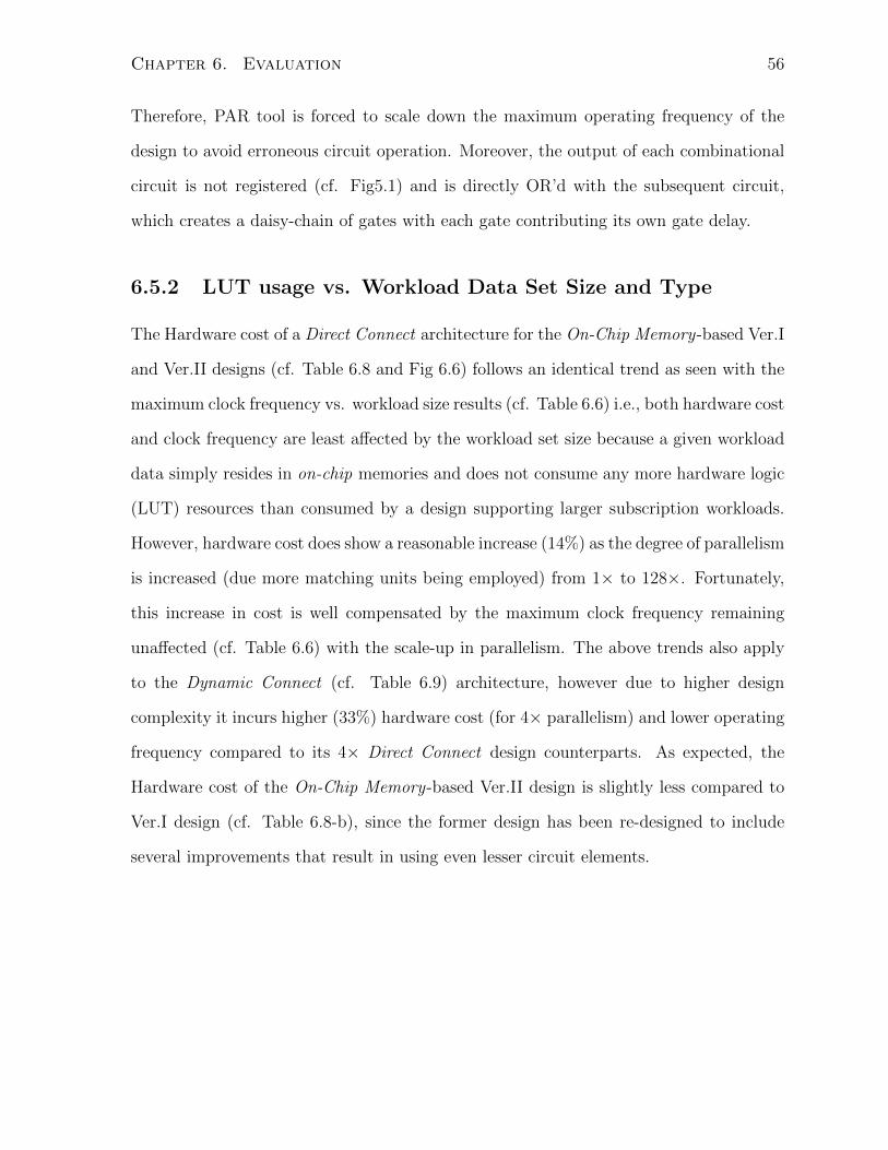
Chapter 6. Evaluation 56
Therefore, PAR tool is forced to scale down the maximum operating frequency of the
design to avoid erroneous circuit operation. Moreover, the output of each combinational
circuit is not registered (cf. Fig5.1) and is directly OR’d with the subsequent circuit,
which creates a daisy-chain of gates with each gate contributing its own gate delay.
6.5.2 LUT usage vs. Workload Data Set Size and Type
The Hardware cost of a Direct Connect architecture for the On-Chip Memory-based Ver.I
and Ver.II designs (cf. Table 6.8 and Fig 6.6) follows an identical trend as seen with the
maximum clock frequency vs. workload size results (cf. Table 6.6) i.e., both hardware cost
and clock frequency are least affected by the workload set size because a given workload
data simply resides in on-chip memories and does not consume any more hardware logic
(LUT) resources than consumed by a design supporting larger subscription workloads.
However, hardware cost does show a reasonable increase (14%) as the degree of parallelism
is increased (due more matching units being employed) from 1× to 128×. Fortunately,
this increase in cost is well compensated by the maximum clock frequency remaining
unaffected (cf. Table 6.6) with the scale-up in parallelism. The above trends also apply
to the Dynamic Connect (cf. Table 6.9) architecture, however due to higher design
complexity it incurs higher (33%) hardware cost (for 4× parallelism) and lower operating
frequency compared to its 4× Direct Connect design counterparts. As expected, the
Hardware cost of the On-Chip Memory-based Ver.II design is slightly less compared to
Ver.I design (cf. Table 6.8-b), since the former design has been re-designed to include
several improvements that result in using even lesser circuit elements.
Chapter 6. Evaluation 57
LUT Usage (design Complexity) vs. Level of Parallelism in Direct
Connect Design
24462845
6253
18280
25122823
6253
2662 2844
6699
32432673
0
2000
4000
6000
8000
10000
12000
14000
16000
18000
20000
1x MU 4x MUs 32x MUs 128x MUs
Level of Parallelism
LU
T U
sag
e
250
500
1000
10K
15K
20K
Figure 6.6: LUT Usage (or design complexity) comparison based on Table6.8

Chapter 6. Evaluation 58
Table a: LUT Usage for Direct Connect (N×HW Ver.I) Design
*Workload 1× MU 4× MUs 32× MUs 128× MUs
250 2446 (8.5%) 2845 (9.9%) 6253 (21.7%) 18280 (63.5%)
500 2435 (8.5%) 2823 (9.8%) 6253 (21.7%) n/a
1K 2512 (8.7%) 2823 (9.8%) 6253 (21.7%) n/a
10K 2570 (8.9%) 3198 (11.1%) 6564 (22.8%) n/a
15K 2662 (9.2%) 2844 (9.9%) 6699 (23.3%) n/a
20k 2673 (9.3%) 3243 (11.3%) n/a n/a
Table b: LUT Usage (scaled) for Direct Connect (N×HW Ver.II) Design
*Workload 1× MU 4× MUs 32× MUs 128× MUs
250 0.91 0.92 0.97 0.99
500 0.92 0.92 0.97 n/a
1K 0.93 0.92 0.97 n/a
10K 0.92 0.94 0.93 n/a
15K 0.93 0.93 0.95 n/a
20k 0.93 0.95 n/a n/a
Table 6.8: Logic Resource Utilization (%LUT) vs. Workload Size (# of subscrip-
tions), as # of MUs is scaled-up in the Direct Connect architecture for
On-chip Memory-based (N×HW ) Ver.I and Ver.II design shown above in
Table a and b respectively. Values in Table b have been scaled for
(N×HW ) Ver.II design with the LUT usage values for Ver.I design
(Table a) for ease of comparison. (* Uniform and Zipfian distributed
propagation workload. n/a - designs failed synthesis due to exhaus-
tion of BRAM resources.)

Chapter 6. Evaluation 59
LUT Usage for On-chip Memory-based Dynamic Connect 4× Design
*Workload LUT (% Usage) Scaled Usage
250 9610 (33.37%) 3.38
500 9890 (34.34%) 3.50
1K 9930 (34.48%) 3.52
10K 9802 (34.03%) 3.07
15K 9816 (34.08%) 3.45
Table 6.9: Logic Resource Utilization (%LUT) vs. Workload Size (# of subscrip-
tions), for a 4× MU Dynamic Connect On-chip Memory-based design. Last
column shows LUT usage scaled with respect to LUT usage for 4×
On-chip Memory-based design synthesized with Uniformly distributed
workload (cf. Table 6.8-a). (* Uniform and Zipfian distributed prop-
agation workloads.)
Furthermore, not only does the LUT usage not vary with Workload set size for all
On-chip Memory-based designs, data in Table 6.10 further shows that the LUT usage
also does not vary with the type of (Unif or Zipf distributed) workload data set either.
Finally, the hardware logic cost of an Index Encoded architecture for the Hardware
Encoded Data-based design (cf. Table 6.11 and Fig.6.11) follows an approximately linear
increase with respect to the workload size due to the increase in combinational circuit
size.
Chapter 6. Evaluation 60
Relative LUT Usage for Direct Connect(N×HW Ver.I) Design With Zipf Workload set
*Workload 1× MU 4× MUs 32× MUs 128× MUs
250 0.99 0.99 1.00 1.00
500 1.00 1.00 1.00 n/a
1K 1.00 1.00 1.00 n/a
10K 1.00 1.00 0.95 n/a
15K 1.00 1.00 1.00 n/a
20k 1.00 1.00 n/a n/a
Table 6.10: Logic Resource Utilization (LUTs) vs. Workload Size (# of sub-
scriptions), as # of MUs is scaled-up in the Direct Connect architec-
ture for On-chip Memory-based design synthesized with Zipf workload
sets. The values have been scaled with respect to LUT usage for On-
chip Memory-based (N×HW Ver.I) design synthesized with Uniform dis-
tributed workload data set (cf. Table 6.8-a). (* Zipfian distributed
propagation workload. n/a - designs failed synthesis due to exhaus-
tion of BRAM resources.)
Chapter 6. Evaluation 61
LUT Usage for Hardware Encoded Design.
*Workload LUT (% Usage) Scaled Usage
250 2338 (8.12%) 0.82
500 2564 (8.90%) 0.91
1K 2976 (10.33%) 1.05
10K 8529 (29.61%) 2.67
20K 13614 (47.27%) 4.20
40K 23226 (80.65%) n/a
Table 6.11: Logic Resource Utilization (%LUTs) vs. Workload Size (# of sub-
scriptions), for the Hardware Encoded data based design. Last column
shows LUT usage scaled with respect to LUT usage for On-chip Mem-
ory-based (4×HW Ver.I) design (cf. Table 6.8-a). (* Uniform and Zip-
fian distributed propagation workloads. n/a - LUT usage unavail-
able for 40K in Table 6.8-a.)

Chapter 6. Evaluation 62
6.5.3 BRAM usage vs. Workload Data Set Size and Type
BRAM (Block RAM) usage for the On-chip Memory-based designs is a critical cost pa-
rameter and depends on the dimension (width and depth) of the memory table being
implemented. The currently used FPGA technology offers 60 64Kbit (or 120 18Kbit)
one dimensional bit array (BRAM) blocks which are partitioned by output multiplexers
to realize user memory tables of various dimensions. For instance in order to implement
a memory table of dimension 96bit wide × 1024 deep (total memory required 96Kbits)
it requires 3 64Kbit blocks each having been partitioned to behave like a two dimen-
sional 96bit wide × 384 deep memory (total memory used 108Kbits). Even though any
arbitrary dimension user memory table may be implemented (few restrictions apply)
however, overall optimal utilization of total available On-chip Memory memory resource
is governed by the dimension (aspect ratio) of the user memory table. For instance in
the previous example, the BRAM memory utilization ratio (total required/total used) is
0.89 or 89% in other words approximately 11% of the BRAM will be wasted. Therefore,
choice of user table aspect ratio governs how much of the FPGA on-chip memory can be
utilized to store useful data which may be important in data intensive applications such
as ours.
BRAM usage for implementing subscription data tables (for uniform distribution
data set) for the Direct Connect architecture On-chip Memory-based designs ((N×HW
Ver.I/II)) is shown in Table6.12-a. As expected BRAM usage is higher for larger work-
load data sets.
A more interesting result to note is how the BRAM utilization deteriorates as the level
of parallelism is scaled up (i.e. when number of memory tables are increased) as shown
in Table6.12-b. This is due to the fact that the dimension of the memory tables cur-
rently implemented does not maximize BRAM utilization, therefore utilization tends to
be lower (e.g. 66.67% for 1x 250 subscription table) at smaller workload data sets as
there is less data available to fully occupy the BRAM memory allocated to implement

Chapter 6. Evaluation 63
Table-a. Sub. Table Dimension vs Block RAM Consumption
*Workload 1 x width x depth 36Kb Block 4 x width x depth 36Kb Block 32 x width x depth 36Kb Block
250 1 x 96 x 512 2 4 x 96 x 512 6 32 x 96 x 80 48
500 1 x 96 x 1024 3 4 x 96 x 512 6 32 x 96 x 92 48
1000 1 x 96 x 1050 5 4 x 96 x 512 6 32 x 96 x 108 48
10K 1 x 96 x 10240 28 4 x 96 x 2600 34 32 x 96 x 410 48
15K 1 x 96 x 15060 41 4 x 96 x 3840 44 32 x 96 x 570 96
20K 1 x 96 x 20070 54 4 x 96 x 5100 56 n/a n/a
Table-a contd.
*Workload 128 x width x depth 36Kb Block
250 128 x 96 x 80 92
500 128 x 96 x 92 n/a
1000 128 x 96 x 108 n/a
10K 128 x 96 x 180 96
15K n/a n/a
20K n/a n/a
Table-b. Sub. Table BRAM Utilization for Unif Workload Data Set
*Workload 1× 4× 32× 128×
250 66.67% 88.89% 13.89% 13.89%
500 88.89% 88.89% 15.97% n/a
1000 54.69% 88.89% 18.75% n/a
10K 95.24% 79.66% 71.18% 62.50%
15K 95.66% 90.91% 49.48% n/a
20K 96.79% 94.87% n/a n/a
Table 6.12: Table-a shows BRAM resource usage (# 36Kbit BRAM blocks) for
data tables of various dimensions vs. Workload Size for # of MUs
in the Direct Connect design. Table-b shows corresponding BRAM uti-
lization for the data tables of various dimensions. (* Unif distribu-
tion type workload set. n/a - designs failed synthesis due to BRAM
exhaustion.)

Chapter 6. Evaluation 64
Sub. Table BRAM Utilization for Zipf Workload Data Set
*Workload 1× 4× 32× 128×
250 66.67% 88.89% 22.22% 22.22%
500 88.89% 88.89% 88.89% n/a
1000 56.25% 88.89% 22.22% n/a
10K 95.24% 80.02% 71.18% 62.50%
15K 96.39% 91.41% 48.78% n/a
20K 97.51% 95.33% 0% n/a
Table 6.13: Shows utilization of dedicated BRAM memory (# 36Kbit BRAM
block) by the subscription data tables of dimension similar to those
shown in Table6.12-A (* Zipfian distributed propagation workload.
n/a - designs failed synthesis due to exhaustion of BRAM resources.)
the table. For the same reason, utilization improves as workload data set size is increased
(e.g. 96.79% for 1x 20K subscription table). Similarly, utilization also drops when the
number of memory tables are increased to scale-up the level of parallelism (e.g. 66.67%
for 1x vs. 13.89% for 128× for 250 subscription table) - again it is due to lesser amount
of useful data being available per table as all data must be equally distributed across
more tables.
BRAM usage is also affected by the type of workload data set. Table6.13 shows
slightly higher BRAM utilization values for the subscription tables containing Zipfian
distribution type workload data set, in comparison to the values obtained for the sub-
scription tables containing Uniform distribution type workload data set (cf. Table 6.12-b).
This variation is due to the distribution characteristic of the Zipfian distribution type
workload data set that contains on average higher number of non-empty clusters than
found in the Uniform distribution type workload data set. This feature results in more

Chapter 6. Evaluation 65
useful data being available (as each non-empty cluster contains at least one subscrip-
tion and an cluster terminator word), especially at smaller size data sets, to occupy the
allocated BRAM memory per table. For example for 250 32× tables the utilization is
22.22% for containing Zipfian distribution type workload data set (cf. Table6.13) vs.
13.89% for similar dimension tables containing Uniform distribution type workload data
set (cf. Table 6.12-b).
6.6 Power Consumption
Power consumption of electronic devices is becoming an important design constraint as
designers must work with ever tighter energy budgets to extend operation on a single
battery charge, while others have to be concerned about rate of thermal dissipation (or
cooling) from the high performance chips as their package (die) size shrink further. We
profile our designs in simulation to gain better insights on how much power is expected
to be consumed and explain the results based on key design features. We used the Xilinx
XPower Analyzer software tool to run post-synthesis power analysis simulations. As
per expectation the power consumption (cf. Table 6.14) for the Direct Connect On-chip
Memory-based (N×HW Ver.I) design increases favourably (logarithmic rise), owing to
the increase in design complexity (higher LUT usage) as the degree of parallelism is
scaled-up. More specifically, it is the increase in Dynamic Power consumption that is
most notable when the designs are scaled-up to higher degrees of parallelism - caused
by increase in switching activity of additional matching units. For example, the 128×
design consumes approximately 4 times more dynamic power than its 4× counterpart
- this represents only 4 times more power consumption for a 32 times scale-up factor.
Hence, data shows that power consumption scale-up is dependent on level of parallelism
for On-chip Memory-based designs.

Chapter 6. Evaluation 66
Power Consumption Vs. Level of Parallelism in Direct Connect(N×HW Ver.I) Design
MUs Quiescent Power Dynamic Power Total Power Clock
1× 0.458W 0.395W 0.853W 129.9Mhz
4× 0.461W 0.448W 0.908W 129.9Mhz
32× 0.482W 0.905W 1.387W 129.9Mhz
128× 0.527W 1.758W 2.286W 129.9Mhz
Table 6.14: Estimated Total (Quiescent, Dynamic) power(Watts) vs. Number of
MUs for all Direct Connect On-chip Memory-based Ver.I design. Data
shows that power consumption scale-up is dependent on level of
parallelism.
Power Consumption Vs. Workload Size and Type for Direct Connect(N×HW Ver.I) Design
*Workload Unif Clock Zipf Clock
250 1.38W (0.48W, 0.90W) 129.9MHz 1.39W (0.48W, 0.91W) 129.9MHz
500 1.38W (0.48W, 0.90W) 129.9MHz 1.39W (0.48W, 0.91W) 129.9MHz
1K 1.38W (0.48W, 0.90W) 129.9MHz 1.39W (0.48W, 0.91W) 129.9MHz
10K 1.38W (0.48W, 0.90W) 129.9MHz 1.39W (0.48W, 0.91W) 129.9MHz
15K 1.38W (0.48W, 0.90W) 129.9MHz 1.39W (0.48W, 0.91W) 129.9MHz
Table 6.15: Estimated Total (Quiescent, Dynamic) power(Watts) vs. Workload
Type (both Uniform and Zipfian) Workload (# of subscriptions) for
a 32xMUs Direct Connect On-chip Memory-based Version I design. Data
shows that power consumption is neither affected by workload dis-
tribution nor size.

Chapter 6. Evaluation 67
Table 6.15 compares between the power consumption exhibited by the Direct Connect
On-chip Memory-based (32xHW Ver.I) design synthesized with Uniform and Zipfian
distribution type workload data sets of various sizes. The data indicates that both
workload data size and type has no impact on the total power consumption. This is
due to the fact that workload data simply resides in on-chip memory and thus does not
necessarily increase the design complexity in the same way the scale-up in the level of
parallelism does (cf. 6.8). Hence, power consumption is neither affected by workload
distribution nor size for On-chip Memory-based designs.
Slightly lower design complexity of the Direct Connect N×HW Ver.II design (as it
utilizes only 93% of LUTs compared to N×HW Ver.I design (cf. Table6.8-b)), is reflected
in its slightly lower (2% less) power consumption (cf. Table 6.16) when compared to its
(N×HW Ver.I) counterpart (cf. Table 6.14).
Conversely, the Dynamic Connect 4× design being more complex, utilizing approxi-
mately 3.5 times more LUTs compared to N×HW Ver.I design (cf. Table6.9), ends up
consuming approximately 1.38 times more power compared to its Direct Connect 4× HW
Ver.I counterpart (cf. Table 6.17).
The above correlation between design complexity (LUT usage) and power consump-
tion is also shown in Graph 6.7.
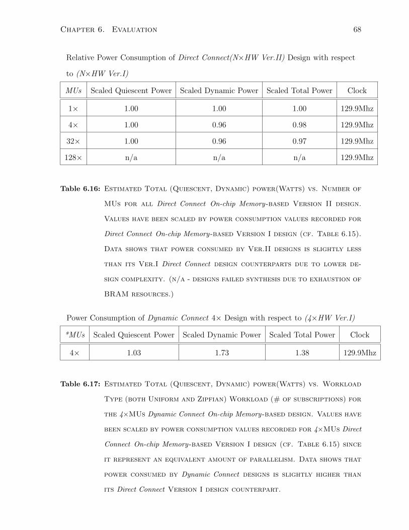
Chapter 6. Evaluation 68
Relative Power Consumption of Direct Connect(N×HW Ver.II) Design with respect
to (N×HW Ver.I)
MUs Scaled Quiescent Power Scaled Dynamic Power Scaled Total Power Clock
1× 1.00 1.00 1.00 129.9Mhz
4× 1.00 0.96 0.98 129.9Mhz
32× 1.00 0.96 0.97 129.9Mhz
128× n/a n/a n/a 129.9Mhz
Table 6.16: Estimated Total (Quiescent, Dynamic) power(Watts) vs. Number of
MUs for all Direct Connect On-chip Memory-based Version II design.
Values have been scaled by power consumption values recorded for
Direct Connect On-chip Memory-based Version I design (cf. Table 6.15).
Data shows that power consumed by Ver.II designs is slightly less
than its Ver.I Direct Connect design counterparts due to lower de-
sign complexity. (n/a - designs failed synthesis due to exhaustion of
BRAM resources.)
Power Consumption of Dynamic Connect 4× Design with respect to (4×HW Ver.I)
*MUs Scaled Quiescent Power Scaled Dynamic Power Scaled Total Power Clock
4× 1.03 1.73 1.38 129.9Mhz
Table 6.17: Estimated Total (Quiescent, Dynamic) power(Watts) vs. Workload
Type (both Uniform and Zipfian) Workload (# of subscriptions) for
the 4×MUs Dynamic Connect On-chip Memory-based design. Values have
been scaled by power consumption values recorded for 4×MUs Direct
Connect On-chip Memory-based Version I design (cf. Table 6.15) since
it represent an equivalent amount of parallelism. Data shows that
power consumed by Dynamic Connect designs is slightly higher than
its Direct Connect Version I design counterpart.

Chapter 6. Evaluation 69
Lastly we look at the power consumption profile exhibited by the Hardware Encoded
data-based Index Encoded design. Data in Table 6.18 suggests, as expected, the power
consumption to be affected by the size of the workload data set since each subscription
is encoded as a combinatorial circuit, thus larger data set design will be more complex,
however it manages to consume less amount of power when compared with the two On-
chip Memory-based designs for every workload data set size. For instance, the increase
in design complexity incurred moving from 250 to 10K subscription in the Index En-
coded design is approximately 20% (cf. Table 6.11 and Graph 6.7) which corresponds
to approximately 130% increase in power consumption (cf. Table 6.18), yet the design
only consumes approximately 48% less power compared to that consumed by the Direct
Connect (128× HW Ver.I) counterpart (cf. Table 6.19). (Power consumption estimate
was performed using maximum clock frequency the complete system is synthesized to
operate at, which is constrained by the clock supported by the target FPGA board.).
Hence, The power consumption profile for Hardware Encoded data-based design is not
affected by workload distribution, but is affected by workload size only.
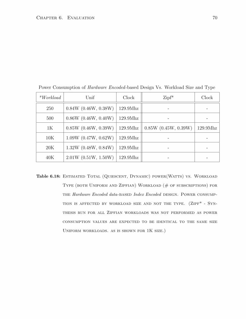
Chapter 6. Evaluation 70
Power Consumption of Hardware Encoded -based Design Vs. Workload Size and Type
*Workload Unif Clock Zipf* Clock
250 0.84W (0.46W, 0.38W) 129.9Mhz - -
500 0.86W (0.46W, 0.40W) 129.9Mhz - -
1K 0.85W (0.46W, 0.39W) 129.9Mhz 0.85W (0.45W, 0.39W) 129.9Mhz
10K 1.09W (0.47W, 0.62W) 129.9Mhz - -
20K 1.32W (0.48W, 0.84W) 129.9Mhz - -
40K 2.01W (0.51W, 1.50W) 129.9Mhz - -
Table 6.18: Estimated Total (Quiescent, Dynamic) power(Watts) vs. Workload
Type (both Uniform and Zipfian) Workload (# of subscriptions) for
the Hardware Encoded data-based Index Encoded design. Power consump-
tion is affected by workload size and not the type. (Zipf* - Syn-
thesis run for all Zipfian workloads was not performed as power
consumption values are expected to be identical to the same size
Uniform workloads. as is shown for 1K size.)
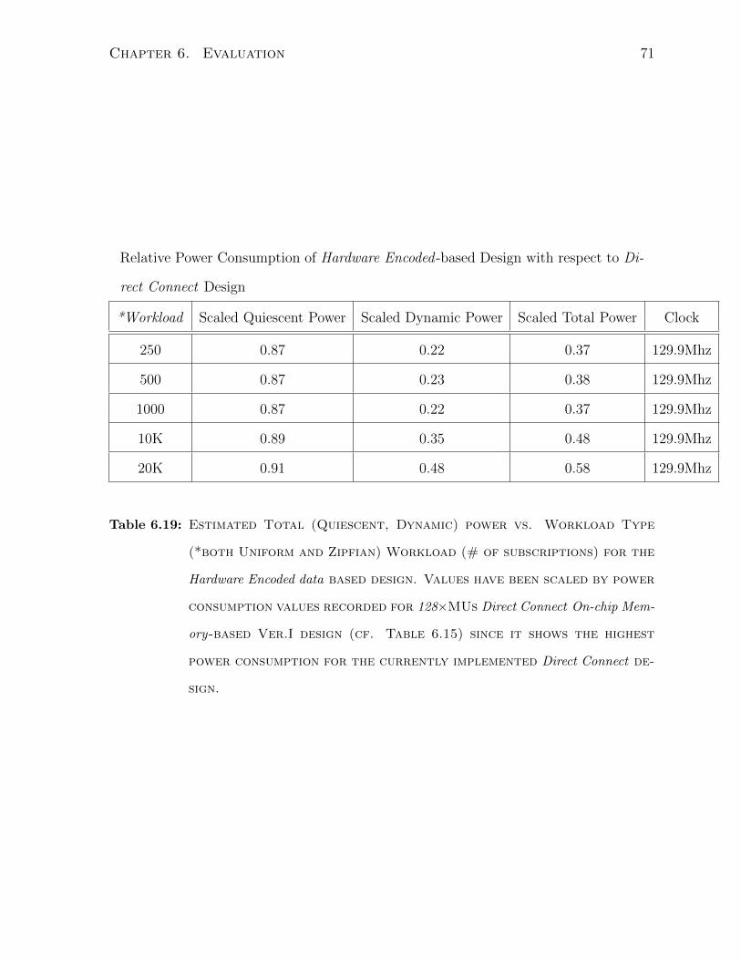
Chapter 6. Evaluation 71
Relative Power Consumption of Hardware Encoded -based Design with respect to Di-
rect Connect Design
*Workload Scaled Quiescent Power Scaled Dynamic Power Scaled Total Power Clock
250 0.87 0.22 0.37 129.9Mhz
500 0.87 0.23 0.38 129.9Mhz
1000 0.87 0.22 0.37 129.9Mhz
10K 0.89 0.35 0.48 129.9Mhz
20K 0.91 0.48 0.58 129.9Mhz
Table 6.19: Estimated Total (Quiescent, Dynamic) power vs. Workload Type
(*both Uniform and Zipfian) Workload (# of subscriptions) for the
Hardware Encoded data based design. Values have been scaled by power
consumption values recorded for 128×MUs Direct Connect On-chip Mem-
ory-based Ver.I design (cf. Table 6.15) since it shows the highest
power consumption for the currently implemented Direct Connect de-
sign.
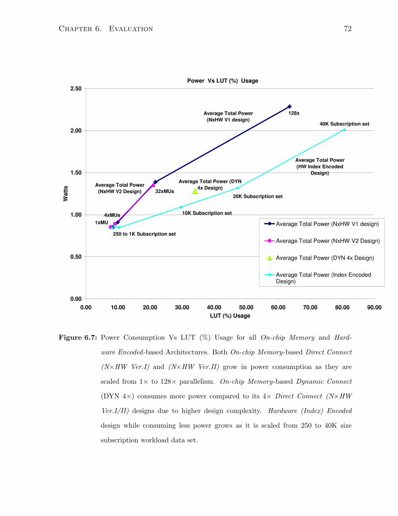
Chapter 6. Evaluation 72
Power Vs LUT (%) Usage
Average Total Power
(NxHW V1 design)
128x
1xMU
Average Total Power
(NxHW V2 Design) 32xMUs
4xMUs
Average Total Power (DYN
4x Design)
20K Subscription set
10K Subscription set
250 to 1K Subscription set
Average Total Power
(HW Index Encoded
Design)
40K Subscription set
0.00
0.50
1.00
1.50
2.00
2.50
0.00 10.00 20.00 30.00 40.00 50.00 60.00 70.00 80.00 90.00
LUT (%) Usage
Watt
s
Average Total Power (NxHW V1 design)
Average Total Power (NxHW V2 Design)
Average Total Power (DYN 4x Design)
Average Total Power (Index EncodedDesign)
Figure 6.7: Power Consumption Vs LUT (%) Usage for all On-chip Memory and Hard-
ware Encoded -based Architectures. Both On-chip Memory-based Direct Connect
(N×HW Ver.I) and (N×HW Ver.II) grow in power consumption as they are
scaled from 1× to 128× parallelism. On-chip Memory-based Dynamic Connect
(DYN 4×) consumes more power compared to its 4× Direct Connect (N×HW
Ver.I/II) designs due to higher design complexity. Hardware (Index) Encoded
design while consuming less power grows as it is scaled from 250 to 40K size
subscription workload data set.

Chapter 6. Evaluation 73
6.7 Summary Of Results
This section summarizes the results and highlights the key findings from data presented
in previous sections.
6.7.1 Designs Under Test
To reiterate the following designs are implemented and evaluated
1. On-chip Memory-based Direct Connect design Version I: N×HW Ver.I.
Design Features:
(a) Uses BRAM based memory tables to store subscription data.
(b) Every cluster data is distributed evenly across all BRAM memory tables.
(c) Parallelism is scaled-up by employing more (1×, 4× and 32×) matching units
(MUs) (cf. Fig. 4.3) with maximum of 20K subscription supported.
(d) Interface between each MUs and its dedicated memory table is direct (cf.
Fig. 4.1).
(e) Hash calculation and cluster index-lookup stage is not pipelined.
2. On-chip Memory-based Direct Connect design Version II: N×HW Ver.II.
Design Features:
(a) Similar in functionality and design and the maximum subscription supported
compared to N×HW Ver.I design.
(b) Design complexity is approx. on average is 7% less compared to N×HW Ver.I
design due to design streamlining (cf. Table 6.8-c).
(c) Hash calculation stage and cluster index-lookup stage has been pipelined.
3. On-chip Memory-based Dynamic Connect (DYN 4×) design.
Design Features:

Chapter 6. Evaluation 74
(a) Uses BRAM based memory tables to store subscription data.
(b) Uses four custom built variable bandwidth (1x to 4x) memory controller
(VbMC) (cf. Fig. 4.4).
(c) Interface between each MUs and all four VbMc is via a Cross-bar based inter-
connect (cf. Fig. 4.5).
(d) Each cluster is allocated entirely to a BRAM memory table. (i.e. cluster data
is not distributed.)
(e) Maximum of 15K subscription supported.
(f) Hash calculation and cluster index-lookup stage is pipelined.
4. Hardware Encoded -based Index Encoded (HW-ENC) design. Design Features:
(a) Subscription data is encoded as combinatoric circuits (cf. Fig. 5.1).
(b) Parallelism is maximal as each subscription is matched in one cycle.
(c) Maximum of 40K subscription supported.
6.7.2 Latency Vs Workload Size
Processing latency in terms of number of clock cycles spent matching a publication event
increases for all On-chip Memory-based Direct Connect and Dynamic Connect designs
as workload size being processed is increased. This trend is validated by the latency
measurement data obtained from both simulations and on-board tests.
In graphs 6.8 and 6.9 latency grows sharply for On-chip Memory-based Direct Connect
designs with lower level of parallelism than it does for designs with higher parallelism
(e.g. 1×HW Ver.I vs. 32×HW Ver.I) as the effective size of each cluster being processed
per matching unit is the larger in the former case.
Both 4×HW Ver.II (Direct Connect) and 4×DYN (Dynamic Connect) exhibit similar
processing latency until 1K workload size then the latter deteriorates in performance for

Chapter 6. Evaluation 75
larger workload sizes (also seen in simulation data cf. Table 6.2). This is due to the 3
cycles per subscription access latency overhead present in the Dynamic Connect designs
which begins to show its prominence (cf. Section6.3.2) at larger workload data sets when
the cluster sizes are large.
Hardware encoded designs are immune to the increase in workload size (cf. Graph 6.8
and 6.9) and exhibit constant processing latency in terms of clock cycles spent matching
an event (cf. Section 6.5) as all subscriptions are encoded as combinatoric circuits which
are run in parallel. However, scaling-up to support larger workload data set sizes does
deteriorate the maximum clock frequency the design can be run at (cf. Table6.7) due to
the increase in design complexity.

Chapter 6. Evaluation 76
Average Latency (cycles) for NxHW Ver.I vs. Workload Size
0
200
400
600
800
1000
1200
250 500 1K 10K 15K
Workload Size
Late
ncy (
Cycle
s)
1x MU (Unif)
4x MU (Unif)
32x MU (Unif)
1x MU (ZIPF)
4x MU (Zipf)
32x MU (Zipf)
4x DYN (Unif)
4x DYN (Zipf)
HW Encoded (Unif &Zipf)
Figure 6.8: Average Latency vs. Workload Size for N×HW Ver.I and all other
designs synthesized for both Uniform and Zipfian distribution type
of workload data set. (Latency measurement data was extracted
from on-board tests.)
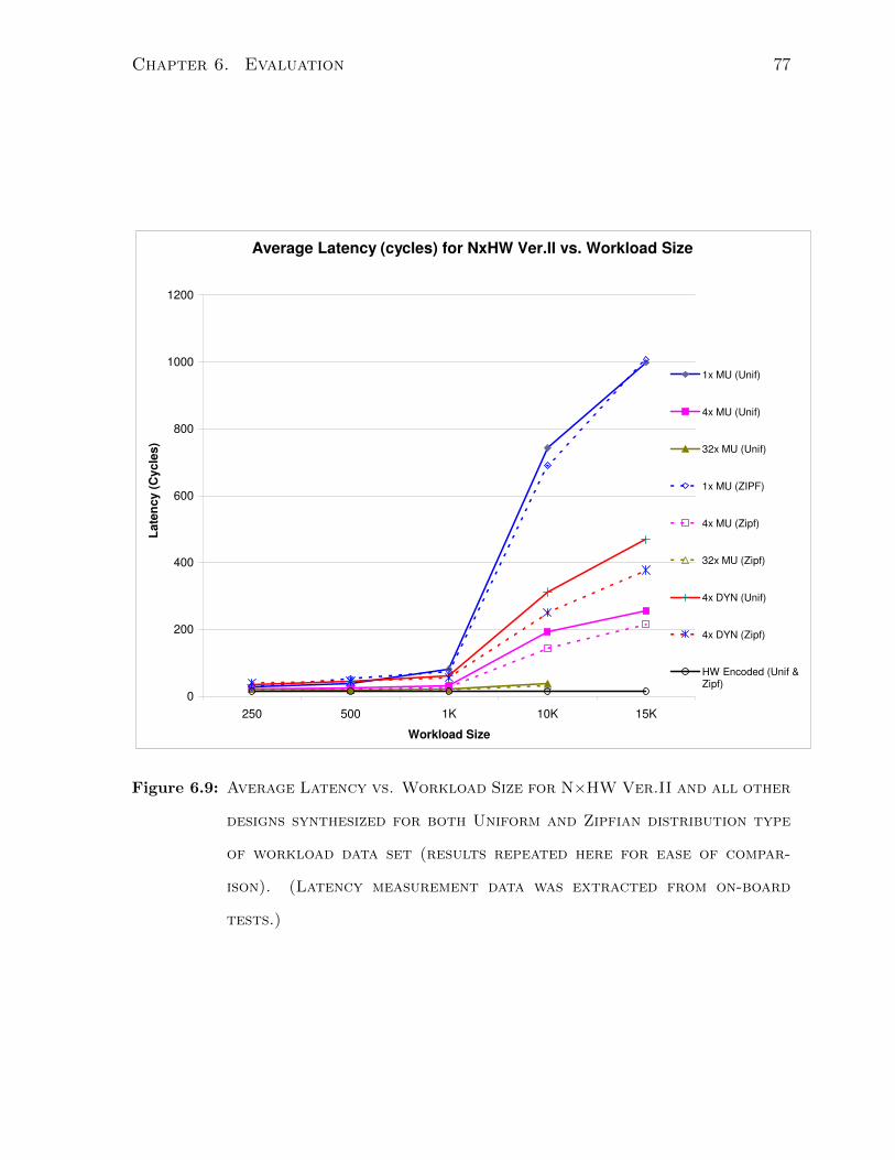
Chapter 6. Evaluation 77
Average Latency (cycles) for NxHW Ver.II vs. Workload Size
0
200
400
600
800
1000
1200
250 500 1K 10K 15K
Workload Size
Late
ncy (
Cycle
s)
1x MU (Unif)
4x MU (Unif)
32x MU (Unif)
1x MU (ZIPF)
4x MU (Zipf)
32x MU (Zipf)
4x DYN (Unif)
4x DYN (Zipf)
HW Encoded (Unif &Zipf)
Figure 6.9: Average Latency vs. Workload Size for N×HW Ver.II and all other
designs synthesized for both Uniform and Zipfian distribution type
of workload data set (results repeated here for ease of compar-
ison). (Latency measurement data was extracted from on-board
tests.)
Chapter 6. Evaluation 78
6.7.3 Max.Clock Rate and LUT Usage Vs Workload Size
Maximum operating frequency for the On-chip Memory-based Direct Connect and Dy-
namic Connect designs remains unaffected as the workload data set size is swept (cf.
Graph 6.11). This is due to design complexity (LUT usage) being un-affected by the
increase in on-chip BRAM usage as the workload size is increased (cf. Fig 6.10).
Design complexity of Hardware Encoded -based designs is proportional to the workload
data set size, hence it affects the maximum operating clock frequency the design can be
run at, which ultimately affects the processing throughput and latency. However, the
rate of deterioration of maximum clock frequency supported in Hardware Encoded -based
designs is less pronounced than the rate of increase in processing latency incurred by
the On-chip Memory-based designs as the workload data set size is scaled-up (cf. Graph
6.8 and 6.9)). Therefore, the affect of workload data set size on the overall processing
latency is expected to be more evident (starting at smaller workload sizes) on the On-chip
Memory-based designs than it would be in case of the Hardware Encoded -based designs.

Chapter 6. Evaluation 79
Max. Clock Rate (Mhz) Supported Vs Workload Size
0
50
100
150
200
250
300
350
250 500 1K 10K 30K 40KWorkload Size
Fre
q.
(Mh
z)
Hardware Encoded Design
1x Direct Connect
4x to 128x Direct Connect
4x Dynamic Connect
Figure 6.10: Max. operating clock rate supported by various designs as work-
load data size is increased. Only the Hardware Encoded design deteri-
orates in Max. operating clock rate when synthesized to support
larger workload data sets.

Chapter 6. Evaluation 80
LUT Usage Vs Workload Size
0
5000
10000
15000
20000
25000
250 500 1K 10K 15K 20K
Workload Size
LU
Ts
1x Direct Connect
4x Direct Connect
32x Direct Connect
128x Direct Connect
HW Encoded
Figure 6.11: Design Complexity or LUT Usage of On-chip Memory-based designs
does not vary with workload data set size but rather scales-up
proportional to the level of parallelism. However, design com-
plexity of Hardware Encoded design is proportional to the workload
data set size.
Chapter 6. Evaluation 81
6.7.4 BRAM Utilization Ratio
BRAM utilization ratio (Total memory required / Total memory allocated) should be
an important design consideration while fixing the dimension of the (on-chip Memory)
BRAM based memory tables, where the Total memory required is the user demand and
the Total memory allocated depends on the native size of the BRAM blocks available on
the target FPGA technology and the number of such discrete memory blocks allocated
by the synthesis tool to realize the required dimension memory table (cf. Section 6.5.3).
Dimension of the memory tables directly affects the total amount of useful data that
can be stored in total memory allocated for the table and limits the highest level of
parallelism that can be supported by the design - i.e. before all BRAM resources are
exhausted.
BRAM utilization deteriorates as the level of parallelism is increased in the on-chip
Memory-based designs for a given workload data set size but it improves as workload
data set size is increased at a given level of parallelism. Therefore, there is an optimal
level of parallelism for a given workload size that yields a maximum BRAM utilization
ratio. For example we see that the 4× Direct Connect designs yield above 80% utilization
for a majority of workload data set sizes (cf. Graphs 6.12 and 6.13).
BRAM utilization ratios for Zipfian distribution type workload data set are slightly
better compared to the Uniform distribution type workload data set (e.g. BRAM Util.
for 32× MU is 15.9% for 500 unif workload size vs. 88.89% for 500 zipf workload size.
cf. Graphs 6.12 and 6.13). This is becaues, as mentioned previously (cf. Section 6.5.3),
the zipfian type workloads contain on average higher number of non-empty clusters than
found in the Uniform distribution type workload data set, as a result more data is avail-
able to be distributed at higher level of parallelism. Therefore, scaling to higher levels of
parallelism at a given workload usually entails increased wastage of the premium on-chip
Memory resources.

Chapter 6. Evaluation 82
1x MU
4x MU
32x MU
128x MU 250
500
1000
10K
15K
20K
96.79
94.87
95.66
90.91
49.48
95.24
79.66
71.18
62.50
54.69
88.89
18.75
88.89
88.89
15.97
1x MU, 66.67
4x MU, 88.89
32x MU, 13.89
128x MU, 13.89
0.00
10.00
20.00
30.00
40.00
50.00
60.00
70.00
80.00
90.00
100.00
BR
AM
Uti
lizati
on
(%
)
Level of ParallelismWorkload Size
BRAM Utilization vs. Level of Parallelism vs. Unif Workload Size
250
500
1000
10K
15K
20K
Figure 6.12: BRAM Utilization ratio (%) shown for Uniform distribution type
workload data set for the On-chip Memory-based Direct Connect de-
signs (similar results for Dynamic Connect is omitted here for
brevity).
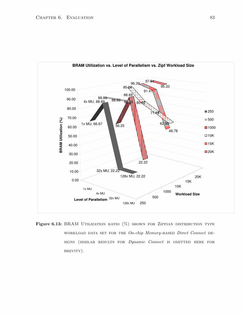
Chapter 6. Evaluation 83
1x MU
4x MU
32x MU
128x MU 250
500
1000
10K
15K
20K
97.51
95.3396.39
91.41
48.78
95.24
80.02
71.18
62.5056.25
88.89
22.22
88.8988.89
88.89
1x MU, 66.67
4x MU, 88.89
32x MU, 22.22
128x MU, 22.22
0.00
10.00
20.00
30.00
40.00
50.00
60.00
70.00
80.00
90.00
100.00
BR
AM
Uti
lizati
on
(%
)
Level of Parallelism
Workload Size
BRAM Utilization vs. Level of Parallelism vs. Zipf Workload Size
250
500
1000
10K
15K
20K
Figure 6.13: BRAM Utilization ratio (%) shown for Zipfian distribution type
workload data set for the On-chip Memory-based Direct Connect de-
signs (similar results for Dynamic Connect is omitted here for
brevity).

Chapter 6. Evaluation 84
6.7.5 Line-rate Processing Comparison
Finally, we compare the throughput of each designs against our initial target of achieving
line-rate processing while performing publish-subscribe matching.
We compare the designs against two types of Line-rate targets: Raw processing
throughput (Mbps) and Message processing throughput (Mmps). Raw processing through-
put takes into account the the bear metal (physical) performance of the design in terms
of amount of data that gets processed per unit time (Mbps - Megabits per second rate) -
this includes rate at which subscription data gets accessed from memory to be matched
against an publication event (cf.Equation 6.1 in Section 6.4 used to calculate raw proc.
throughput). Line-rate target here represents the maximum bit rate supported by the
publication event channel - which in our case is 1000Mbps or 1Gbps Ethernet link.
Raw processing throughput of the Hardware (HW) Encoded -based design exceeds the
line-rate target and remains unaffected by the workload data set size due to its constant
processing latency profile (cf. Section 6.3.3) (throughput is calculated using 14 clock
cycles that are spent to process 4× 32 bit words from the Input Event Queue).
Next, the On-chip Memory-based 32×HW Ver.II design dominates in performance
compared to all other On-chip Memory-based designs this is attributed to to the pipeling
of the Hash calculation stage and other design streamlining (cf. Section 6.3.1).
Lastly, the 4×DYN Dynamic Connect design at smaller (250 to 500) workload data
set sizes tends to perform slightly better than the 32×HW Ver.I design due to diminished
parallelism caused by idling of many data starved matching units, which is exactly the
problem that is rectified by the Dynamic Connect design (cf. Section 4.3.2). However,
the Dynamic Connect design loses due to several overhead taking prominence at larger
workload sizes (cf. Section 6.3.2).
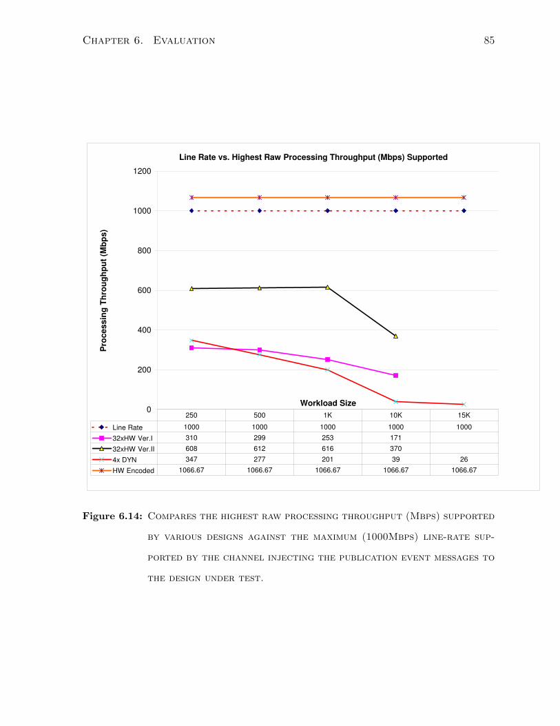
Chapter 6. Evaluation 85
Line Rate vs. Highest Raw Processing Throughput (Mbps) Supported
0
200
400
600
800
1000
1200
Workload Size
Pro
cessin
g T
hro
ug
hp
ut
(Mb
ps)
Line Rate 1000 1000 1000 1000 1000
32xHW Ver.I 310 299 253 171
32xHW Ver.II 608 612 616 370
4x DYN 347 277 201 39 26
HW Encoded 1066.67 1066.67 1066.67 1066.67 1066.67
250 500 1K 10K 15K
Figure 6.14: Compares the highest raw processing throughput (Mbps) supported
by various designs against the maximum (1000Mbps) line-rate sup-
ported by the channel injecting the publication event messages to
the design under test.
Chapter 6. Evaluation 86
It is more meaningful to compare the design performance against the Line-rate target
which is represented in terms of the maximum number of event messages that can be
delivered by the channel per unit time (Mmps - Mega messages per second) - calculated
using the delivery time for a 64byte frame on a 1Gbps Ethernet link.
Message processing throughput for each design is the reciprocal of the average pro-
cessing latency incurred per publication event message (cf. Graph 6.8 and 6.9) (cf.
Equation 6.2 in Section 6.4 used to calculate message proc. throughput).
Message (Event) processing throughput of the Hardware (HW) Encoded -based design
dominates again due to the unprecedented level of parallelism offered by the design such
that all publication event messages are processed under 14 clock cycles irrespective of the
workload data set size (cf. Section 6.3.3). All other designs also outperform with respect
to the message processing line-rate target (cf. Graph 6.15).

Chapter 6. Evaluation 87
Line Rate vs. Highest Message Processing Throughput (Mmps) Supported
0.00
1.00
2.00
3.00
4.00
5.00
6.00
7.00
8.00
9.00
Workload Size
Meg
a m
essag
es p
er
seco
nd
(M
mp
s)
Line Rate 1.95 1.95 1.95 1.95 1.95
32xHW Ver.I 3.0 3.0 3.0 2.2
32xHW Ver.II 6.3 6.4 6.4 2.2
4x DYN 3.6 2.9 2.1 0.4 0.3
HW Encoded 8.33 8.33 8.33 8.33 8.33
250 500 1K 10K 15K
Figure 6.15: Compares the highest event processing throughput (Mmps) sup-
ported by various designs against the maximum (2.0 Mmps) message
line-rate supported by the channel injecting the publication event
messages to the design under test.

Chapter 7
Conclusions & Future Work
Our vision is to meet the line-rate middleware challenge that is at the core of many event
processing scenarios such as real-time data analytics and financial applications. Further-
more, to enable the high-frequency and low-latency requirements of these applications,
we presented an efficient event processing platform over reconfigurable hardware that
exploits the high degrees of hardware parallelism for achieving line-rate processing. In
short, the success of our fpga-ToPSS framework is through the use of reconfigurable hard-
ware (i.e., FPGAs) that enables on-board packet processing and hardware acceleration
for matching through custom logic circuits. Our hardware solution not only eliminates
the OS layer latency, but also achieves an unprecedented level of parallelism not available
to pure software solutions.
We ultimately envision moving towards the heterogeneous architectures hosting both
FPGAs and CPUs for the next generation of middleware applications. This vision,
which extends our current framework, is motivated by the emergence of FPGA-based
co-processors on motherboards (e.g., Intel Xeon FSB FPGA Socket Fillers by Nallatech)
integrated via high bandwidth interconnects (64-bit 1066MHz FSB), with up to 256GB
direct system memory access and a 8GB/s peak bandwidth. This is a promising platform
for transforming cutting edge event processing applications to achieve real-time complex
88

Chapter 7. Conclusions & Future Work 89
data analysis by orchestrating computations across FPGAs and CPUs.

Appendix A
Dynamic Connect - Implementation
Detail
Figure A.1: 4×VbMc. A variable width (BWreq) sliding window is used to sched-
ule reads from the dual-port BRAM unit to have subscriptions
ready prior to be shifted into output shift register array.
A.1 Variable Bandwidth Memory Controller
A VbMc (Variable Bandwidth Memory Controller) (cf. Fig A.1) is a wrapper design
build around a conventional dual-port BRAM unit (each port may be independently
addressed). VbMc mimics a memory controller that can variably output either one (1×)
90

Appendix A. Dynamic Connect - Implementation Detail 91
to a maximum of P (P×) number of subscriptions per cycle, where P is number of VbMC
output ports or maximum output bandwidth supported. For this project, a 4× VbMc has
been implemented. It is also essential that BRAM units store P subscriptions per address
entry in order to keep memory access latency uniform upto P× operating mode. Inputs
to the VbMc: BWreq is Bandwidth requested in previous cycle, E.g. 0× - indicates null
request, 1× - left shifts all subscriptions by one from all 4 output ports while shifting a new
subscription into the last port (PortA ← PortB ← PortC ← PortD ← new sub) . . .
4× - performs no left shift as all output ports need to be refreshed with new subscriptions
for each (PortA ← new sub0, PortB ← new sub1, PortC ← new sub2, PortD ←
new sub3). The Address input (value computed during the cluster index lookup step
(Sec 4.2.1)) is used to initialize the VbMc to the beginning of a cluster stored in its
BRAM unit. Besides, the VbMc’s output data ports is the BWavl output that indicates
the maximum bandwidth the VbMc can satisfy for the next request cycle: E.g. 0× -
indicates zero subscriptions remaining to be read for the next request, .. 3× - indicates
only 3 subscriptions remaining before cluster ends, 4× - indicates maximum number of
subscription remaining before cluster ends since VbMc has no knowledge of the cluster
until the cluster end marker enters into its 4× shift window. Major design challenges
encountered were particularly with implementing the logic responsible for computing
dual-port BRAM address pointers while considering wrap around of the sliding window
and scheduling the reads to avoid stalling of the output shift registers (cf. Fig A.1). The
current 4×VbMc is synthesized to operate at 372.583MHz max, while consuming:1776
Slice LUTs & 375 Slice Registers.
A.1.1 Crossbar
The crossbar(Xbar) design (cf. Fig A.2) implemented for the project is essentially a
monolithic 16-to-1 multiplexer with 80 bit wide ports selected as a result of evalu-
ating two other designs in terms of operating frequency and resource utilization. The
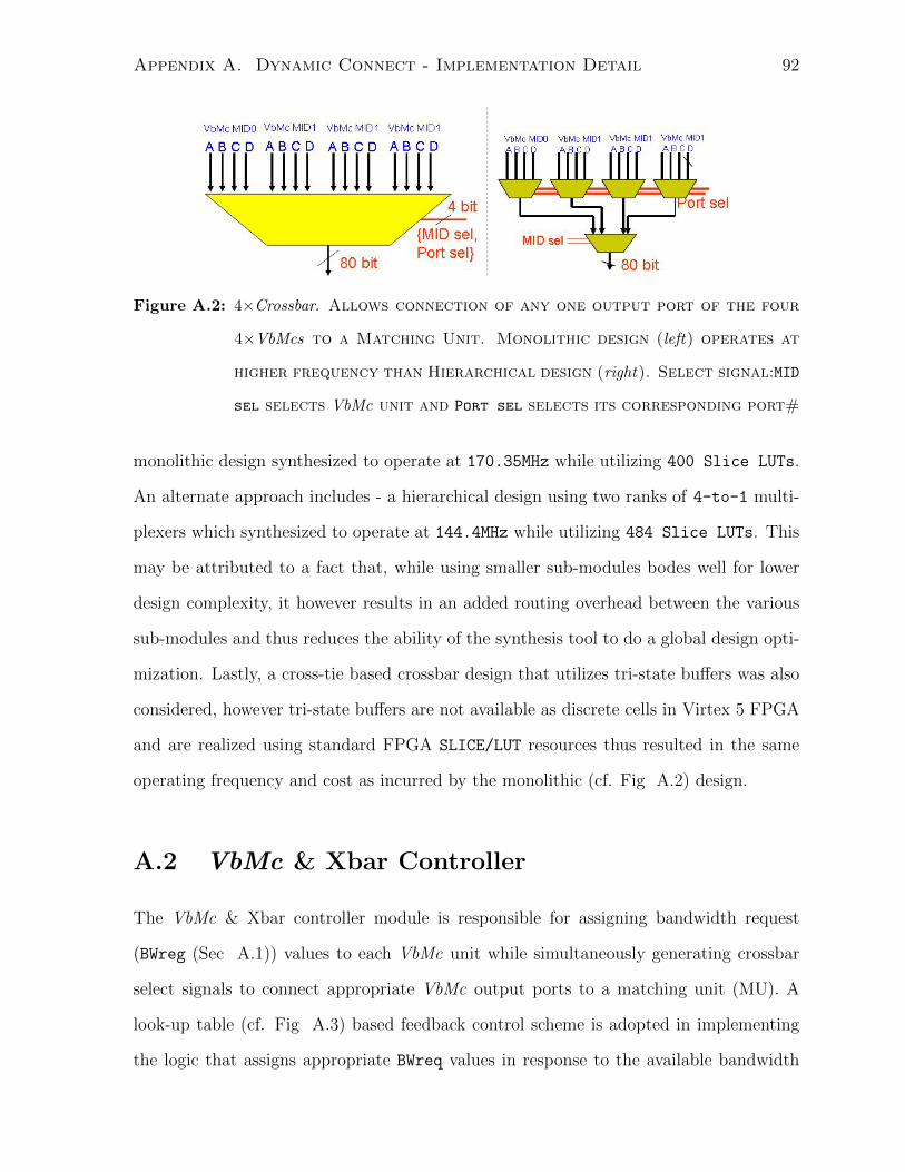
Appendix A. Dynamic Connect - Implementation Detail 92
Figure A.2: 4×Crossbar. Allows connection of any one output port of the four
4×VbMcs to a Matching Unit. Monolithic design (left) operates at
higher frequency than Hierarchical design (right). Select signal:MID
sel selects VbMc unit and Port sel selects its corresponding port#
monolithic design synthesized to operate at 170.35MHz while utilizing 400 Slice LUTs.
An alternate approach includes - a hierarchical design using two ranks of 4-to-1 multi-
plexers which synthesized to operate at 144.4MHz while utilizing 484 Slice LUTs. This
may be attributed to a fact that, while using smaller sub-modules bodes well for lower
design complexity, it however results in an added routing overhead between the various
sub-modules and thus reduces the ability of the synthesis tool to do a global design opti-
mization. Lastly, a cross-tie based crossbar design that utilizes tri-state buffers was also
considered, however tri-state buffers are not available as discrete cells in Virtex 5 FPGA
and are realized using standard FPGA SLICE/LUT resources thus resulted in the same
operating frequency and cost as incurred by the monolithic (cf. Fig A.2) design.
A.2 VbMc & Xbar Controller
The VbMc & Xbar controller module is responsible for assigning bandwidth request
(BWreg (Sec A.1)) values to each VbMc unit while simultaneously generating crossbar
select signals to connect appropriate VbMc output ports to a matching unit (MU). A
look-up table (cf. Fig A.3) based feedback control scheme is adopted in implementing
the logic that assigns appropriate BWreq values in response to the available bandwidth

Appendix A. Dynamic Connect - Implementation Detail 93
Figure A.3: VbMc & Xbar Control Table. Lookup address is formed by concatenating
the sampled available bandwidth (here 3× for MID0 & MID1) values.
Each 32 bit table entry contains BWreq assignments and Xbar select
signals
(BWavl (Sec A.1)) values (Table is compiled by using a script prior to design synthe-
sis). This module constantly cycles between states SAMPLE (when all BWavl values are
sampled) → READ TABLE (control table is looked-up) → HOLD (BWreq and Xbar select
signals are asserted and held valid until MUs acknowledge back for new subscriptions).
The control table stores for each permutation of system state (captured by concatenating
all BWavl values), the appropriate assignments of BWreg and Xbar control signals (MID
sel, Port sel cf. Fig A.2) values for each VbMc unit and crossbar dedicated to each
MU respectively.
An obvious advantage of having a table based control scheme is a resulting design that
is cheap (consuming: 67 Slice LUTs & 14 Slice Registers) and fast (synthesized to
operate at 615.764MHz) however, the size of the control table becomes prohibitively large
as number of VbMc units per design are increased. Nonetheless, several optimizations are
possible to reduce the number of states that are required to be stored in this table. One
such optimization that is implemented in this project is one that truncates each sampled
BWavl value to just 2 bits (i.e. only BWavl 0× to 3× are used in constructing the table
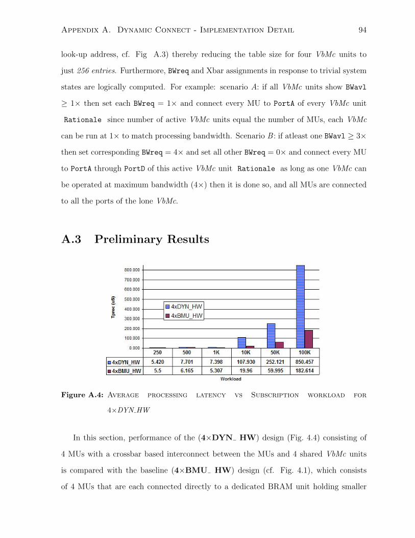
Appendix A. Dynamic Connect - Implementation Detail 94
look-up address, cf. Fig A.3) thereby reducing the table size for four VbMc units to
just 256 entries. Furthermore, BWreq and Xbar assignments in response to trivial system
states are logically computed. For example: scenario A: if all VbMc units show BWavl
≥ 1× then set each BWreq = 1× and connect every MU to PortA of every VbMc unit
Rationale since number of active VbMc units equal the number of MUs, each VbMc
can be run at 1× to match processing bandwidth. Scenario B : if atleast one BWavl ≥ 3×
then set corresponding BWreq = 4× and set all other BWreq = 0× and connect every MU
to PortA through PortD of this active VbMc unit Rationale as long as one VbMc can
be operated at maximum bandwidth (4×) then it is done so, and all MUs are connected
to all the ports of the lone VbMc.
A.3 Preliminary Results
Figure A.4: Average processing latency vs Subscription workload for
4×DYN HW
In this section, performance of the (4×DYN HW) design (Fig. 4.4) consisting of
4 MUs with a crossbar based interconnect between the MUs and 4 shared VbMc units
is compared with the baseline (4×BMU HW) design (cf. Fig. 4.1), which consists
of 4 MUs that are each connected directly to a dedicated BRAM unit holding smaller
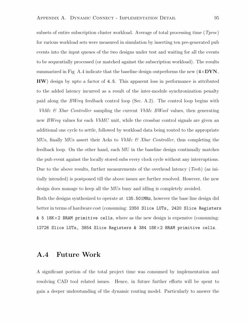
Appendix A. Dynamic Connect - Implementation Detail 95
subsets of entire subscription cluster workload. Average of total processing time (Tproc)
for various workload sets were measured in simulation by inserting ten pre-generated pub
events into the input queues of the two designs under test and waiting for all the events
to be sequentially processed (or matched against the subscription workload). The results
summarized in Fig A.4 indicate that the baseline design outperforms the new (4×DYN
HW) design by upto a factor of 4.5. This apparent loss in performance is attributed
to the added latency incurred as a result of the inter-module synchronization penalty
paid along the BWreq feedback control loop (Sec. A.2). The control loop begins with
VbMc & Xbar Controller sampling the current VbMc BWavl values, then generating
new BWreq values for each VbMC unit, while the crossbar control signals are given an
additional one cycle to settle, followed by workload data being routed to the appropriate
MUs, finally MUs assert their Acks to VbMc & Xbar Controller, thus completing the
feedback loop. On the other hand, each MU in the baseline design continually matches
the pub event against the locally stored subs every clock cycle without any interruptions.
Due to the above results, further measurements of the overhead latency (Tovh) (as ini-
tially intended) is postponed till the above issues are further resolved. However, the new
design does manage to keep all the MUs busy and idling is completely avoided.
Both the designs synthesized to operate at 135.501MHz, however the base line design did
better in terms of hardware cost (consuming: 2350 Slice LUTs, 2420 Slice Registers
& 5 18K×2 BRAM primitive cells, where as the new design is expensive (consuming:
12726 Slice LUTs, 3854 Slice Registers & 384 18K×2 BRAM primitive cells.
A.4 Future Work
A significant portion of the total project time was consumed by implementation and
resolving CAD tool related issues. Hence, in future further efforts will be spent to
gain a deeper understanding of the dynamic routing model. Particularly to answer the

Appendix A. Dynamic Connect - Implementation Detail 96
question, why is it difficult to achieve the theoretical performance gain owing to dynamic
distribution of workload, as anticipated in the project proposal. Several key lessons
were learnt from the design experience. Namely, design hierarchy must be sacrificed (i.e.
design must be flattened) to reduce inter-module handshaking synchronization penalties,
secondly adding buffers at the the output of the cross-bar would help to decouple the
MUs from VbMc & Xbar Controller thus shortening the feedback control loop, lastly it
is much cost efficient to keep the data closer to the processing units to avoid reliance on
interconnect fabric to deliver performance critical data. In consideration of the above
lessons learned, a well educated design decisions could be utilized to further improve the
new design.

Bibliography
[1] Aguilera, M.K., Strom, R.E., Sturman, D.C., Astley, M., Chandra, T.D.: Matching
events in a content-based subscription system. In: PODC’99. pp. 53–61. ACM, New
York, NY, USA (1999)
[2] Auerbach, J., Bacon, D.F., Cheng, P., Rabbah, R.: Lime: a java-compatible and
synthesizable language for heterogeneous architectures. pp. 89–108. OOPSLA’10,
ACM, New York, NY, USA (2010)
[3] Brenna, L., Demers, A., Gehrke, J., Hong, M., Ossher, Panda, Riedewald, Thatte,
White: Cayuga: high-performance event processing engine. SIGMOD’07 pp. 1100–
1102 (2007)
[4] Cranor, C., Johnson, T., Spataschek, O.: Gigascope: a stream database for network
applications. In: SIGMOD’03. pp. 647–651 (2003)
[5] Diao, Y., Fischer, P., Franklin, M., To, R.: Yfilter: Efficient and scalable filtering of
XML documents. In: ICDE’02 (2002)
[6] Fabret, F., Jacobsen, H.A., Llirbat, F., Pereira, J., Ross, K.A., Shasha, D.: Filtering
algorithms and implementation for fast pub/sub systems. SIGMOD’01 pp. 115–126
(2001)
[7] Farroukh, A., Sadoghi, M., Jacobsen, H.A.: Towards vulnerability-based intrusion
detection with event processing. In: DEBS’11. pp. 171–182 (2011)
97

Bibliography 98
[8] Fontoura, M., Sadanandan, S., Shanmugasundaram, J., Vassilvitski, S., Vee, E.,
Venkatesan, S., Zien, J.: Efficiently evaluating complex boolean expressions. In:
SIGMOD’10. pp. 3–14. ACM, New York, NY, USA (2010)
[9] Glavic, B., Esmaili, K.S., Fischer, P.M., Tatbul, N.: The case for fine-grained stream
provenance. In: BTW Workshops’11. pp. 58–61 (2011)
[10] Han, X., et al.: An optical centralized shared-bus architecture demonstrator for
microprocessor-to-memory interconnects. IEEE STQE’03
[11] Harizopoulos, S., Abadi, D.J., Madden, S., Stonebraker, M.: OLTP through the
looking glass, and what we found there. In: SIGMOD’08. pp. 981–992. ACM, New
York, NY, USA (2008)
[12] Ikeda, R., Widom, J.: Panda: A system for provenance and data. IEEE Data Eng.
Bull.’10 33(3), 42–49 (2010)
[13] Johnson, R., Pandis, I., Hardavellas, N., Ailamaki, A., Falsafi, B.: Shore-MT: a
scalable storage manager for the multicore era. In: EDBT’09. pp. 24–35 (2009)
[14] Machanavajjhala, A., Vee, E., Garofalakis, M., Shanmugasundaram, J.: Scalable
ranked publish/subscribe. VLDB’08 1(1), 451–462 (2008)
[15] Misra, A., Blount, M., Kementsietsidis, A., Sow, D., Wang, M.: Provenance and an-
notation of data and processes. In: Freire, J., Koop, D., Moreau, L. (eds.) Springer-
Verlag’08. pp. 253–265. Berlin, Heidelberg (2008)
[16] Mitra, A., et al.: Boosting XML filtering with a scalable FPGA-based architecture.
CIDR’09
[17] Morris, G.W., Thomas, D.B., Luk, W.: FPGA accelerated low-latency market data
feed processing. IEEE: 17th High Performance Interconnects’09 0, 83–89 (2009)

Bibliography 99
[18] Mueller, R., Teubner, J., Alonso, G.: Data processing on FPGAs. VLDB’09 2(1),
910–921 (2009)
[19] Mueller, R., Teubner, J., Alonso, G.: Streams on wires: a query compiler for FPGAs.
VLDB’09 2(1), 229–240 (2009)
[20] Muller, R., Teubner, J., Alonso, G.: Glacier: a query-to-hardware compiler. In:
Elmagarmid, A.K., Agrawal, D. (eds.) SIGMOD’10. pp. 1159–1162. ACM (2010)
[21] Pandis, I., Johnson, R., Hardavellas, N., Ailamaki, A.: Data-oriented transaction
execution. PVLDB’10 3(1), 928–939 (2010)
[22] Sadoghi, M., Burcea, I., Jacobsen, H.A.: GPX-Matcher: a generic Boolean
predicate-based XPath expression matcher. In: EDBT’11. pp. 45–56 (2011)
[23] Sadoghi, M., Jacobsen, H.A.: BE-Tree: an index structure to efficiently match
Boolean expressions over high-dimensional discrete space. In: SIGMOD’11. pp. 637–
648 (2011)
[24] Sadoghi, M., Jacobsen, H.A., Labrecque, M., Shum, W., Singh, H.: Efficient event
processing through reconfigurable hardware for algorithmic trading. PVLDB’11 3(2),
1525–1528 (2010)
[25] Sadoghi, M., Singh, H., Jacobsen, H.A.: Towards highly parallel event processing
through reconfigurable hardware. In: DaMoN’11. pp. 27–32 (2011)
[26] Shukla, S., Rabbah, R., Vorbach, M.: Fpga-based combined architecture for stream
categorization and intrusion detection. In: MEMOCODE’10. pp. 77–80 (2010)
[27] Srivastava, D., Golab, L., Greer, R., Johnson, T., Seidel, J., Shkapenyuk, V.,
Spatscheck, O., Yates, J.: Enabling real time data analysis. PVLDB’10 3(1), 1–
2 (2010)

Bibliography 100
[28] Teubner, J., Mueller, R.: How soccer players would do stream joins. In: Proceedings
of the 2011 international conference on Management of data. pp. 625–636. SIGMOD
’11, ACM, New York, NY, USA (2011)
[29] Teubner, J., Muller, R., Alonso, G.: FPGA acceleration for the frequent item prob-
lem. In: Li, F., Moro, M.M., Ghandeharizadeh, S., Haritsa, J.R., Weikum, G., Carey,
M.J., Casati, F., Chang, E.Y., Manolescu, I., Mehrotra, S., Dayal, U., Tsotras, V.J.
(eds.) ICDE’10. pp. 669–680. IEEE (2010)
[30] Vijayakumar, N., Plale, B.: Tracking stream provenance in complex event processing
systems for workflow-driven computing. In: EDA-PS’07. Vienna, Austria (09/2007
2007)
[31] Whang, S., Brower, C., Shanmugasundaram, J., Vassilvitskii, S., Vee, E., Yerneni,
R., Garcia-Molina, H.: Indexing boolean expressions. In: VLDB’09. Stanford Info-
Lab (2009)
[32] Woods, L., Teubner, J., Alonso, G.: Complex event detection at wire speed with
FPGAs. PVLDB’10 3(1), 660–669 (2010)
[33] Wu, E., Diao, Y., Rizvi, S.: High-performance complex event processing over
streams. In: SIGMOD’06. pp. 407–418. ACM, New York, NY, USA (2006)
[34] Joe Corrigan:Updated Traffic Projections. In:OPRA, March’07.
Options Price Reporting Authority, Mar. 22, ’07. (http :
//opradata.com/specs/2008P rojections.pdf)
[35] Sidhu, R., Prasanna, V., K., : Fast Regular Expression Matching using FPGAs. In:
IEEE Symposium on Field-Programmable Custom Computing Machines(2001).

Bibliography 101
[36] Bispo, J., Sourdis, I., Cardoso, J., M., P., Vassiliadis, S.: Synthesis of Regular
Expressions Targeting FPGAs. In: International Workshop Proceedings’07. pp.179–
190. Springer(2007)