Embed Size (px)
Citation preview
20. - 22. 10. 2009, Rožnov pod Radhoštěm, Česká Republika
TOWARDS ARRAY MICROMANIPULATORS BASED ON DIELECTRIC ELASTOMERS
Martin ŘEZÁČ, Zdeněk HURÁK
Department of Control Engineering, Faculty of Electrical Engineering (FEL), Czech Technical University in Prague (ČVUT),
Karlovo náměstí 13/e, 12135 Praha 2, Česká republika E-mail: [email protected], [email protected]
Abstract
The paper describes the authors' initial steps in the domain of advanced microactuators based on dielectric
elastomers. Namely, local deformation of a thin (~10um) elastomer film as a result of Maxwell pressure on
the surface is analyzed. The pressure results from attractive forces between the opposite charges on the
conducting electrodes deposited on both sides of the polymer film. When at least one of the two electrodes is
compliant, repulsive forces among the alike charges also contribute to the surface deformation. Compared to
the conventional materials such as piezoelectric ceramics, DEA promise much higher strain (nearly 10%)
while keeping reasonable values of other parameters such as efficiency and time response.
The ultimate goal of this initiating research is to develop a deformable surface that could be used for planar
manipulation with flat objects placed on top of it. Induced surface traveling wave, for instance, could be used
to achieve simple transportation of samples in the style of common linear ultrasonic motors.
The early achievements presented in this paper include trivial yet tedious fabrication consisting in sputtering
Cr+Au electrodes on the substrate, then spincoating a ~10um-thick film from a commercially available
elastomer known as PDMS (polydimethyl siloxane, branded as Sylgard 184 by Dow Corning) and finally
depositing the top (compliant) gold electrode, and laboratory experiments with high voltage (around 1kV)
applied to the electrodes. Deformation of the film observed with an optical microscope partially agrees with
the computational model developed in a FEM modeler/solver. The deviations from the model are discussed.
1 INTRODUCTION TO PLANAR ARRAY MICROMANIPULATION
The ultimate goal of the research outlined in this paper is to develop a distributed planar micromanipulator
for steering small (meso or microscale) objects over a flat substrate. The fact that the manipulation will be
spatially distributed promises an increased throughput for various assembly procedures because it allows for
high degree of parallelism compared to inherently traditional high precision microrobotic manipulation
schemes.
Among the most prominent researchers in the field of distributed manipulation is Karl Bohringer. His
monograph [4] gives a good survey. In a long series of papers from the late 1990s he introduces a concept
of a programmable force field [6, 8]. Loosely speaking, it is a mathematical formalism that allows engineers
to calculate control signals for large (dense) arrays of actuators to accomplish a given mission. A
distinguished contribution was made by Luntz and Messner [14] as they were the first to consider some
discreteness issued of the actuator field. Murphey and Burdick elaborated on these mathematically difficult
problems a bit more [15].
20. - 22. 10. 2009, Rožnov pod Radhoštěm, Česká Republika
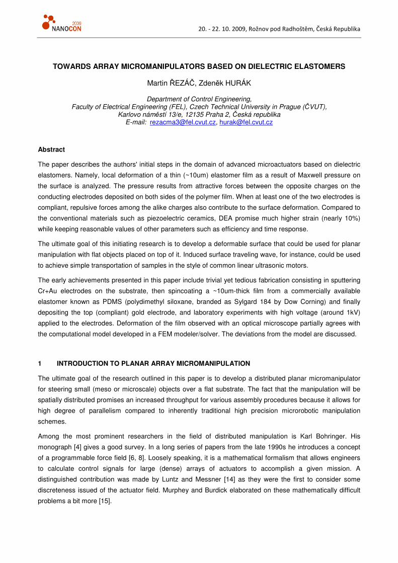
A screenshot of the output from a numerical simulation of such a force field is given in Fig.1. A spatially
discrete array of actuators exerts forces and
moments on object placed onto the surface of
such actuator.
Fig. 1: Simulation of motion of objects in a planar
spatially discrete force field.
2 INTRODUCTION TO DIELECTRIC
ELASTOMER ACTUATORS
The previous section on array micromanipulators
did not give much hint as for the link of this paper
with the field of material engineering and
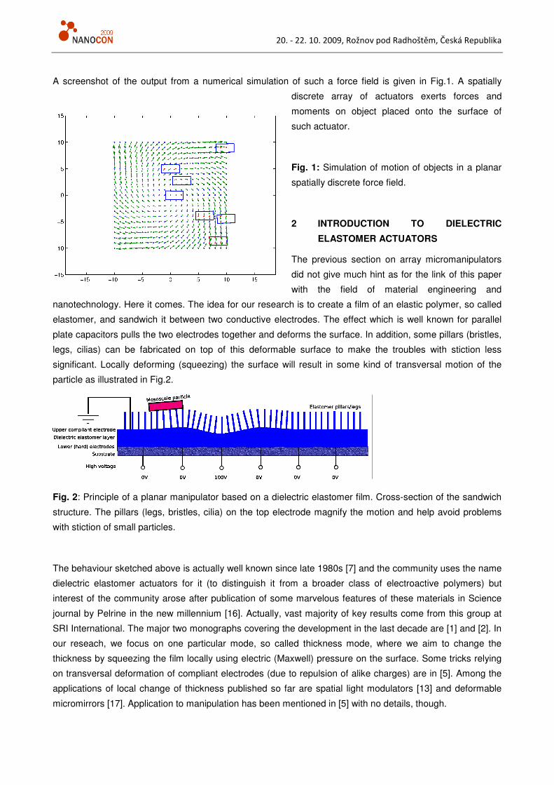
nanotechnology. Here it comes. The idea for our research is to create a film of an elastic polymer, so called
elastomer, and sandwich it between two conductive electrodes. The effect which is well known for parallel
plate capacitors pulls the two electrodes together and deforms the surface. In addition, some pillars (bristles,
legs, cilias) can be fabricated on top of this deformable surface to make the troubles with stiction less
significant. Locally deforming (squeezing) the surface will result in some kind of transversal motion of the
particle as illustrated in Fig.2.
Fig. 2: Principle of a planar manipulator based on a dielectric elastomer film. Cross-section of the sandwich
structure. The pillars (legs, bristles, cilia) on the top electrode magnify the motion and help avoid problems
with stiction of small particles.
The behaviour sketched above is actually well known since late 1980s [7] and the community uses the name
dielectric elastomer actuators for it (to distinguish it from a broader class of electroactive polymers) but
interest of the community arose after publication of some marvelous features of these materials in Science
journal by Pelrine in the new millennium [16]. Actually, vast majority of key results come from this group at
SRI International. The major two monographs covering the development in the last decade are [1] and [2]. In
our reseach, we focus on one particular mode, so called thickness mode, where we aim to change the
thickness by squeezing the film locally using electric (Maxwell) pressure on the surface. Some tricks relying
on transversal deformation of compliant electrodes (due to repulsion of alike charges) are in [5]. Among the
applications of local change of thickness published so far are spatial light modulators [13] and deformable
micromirrors [17]. Application to manipulation has been mentioned in [5] with no details, though.
20. - 22. 10. 2009, Rožnov pod Radhoštěm, Česká Republika
3 FEM SIMULATIONS
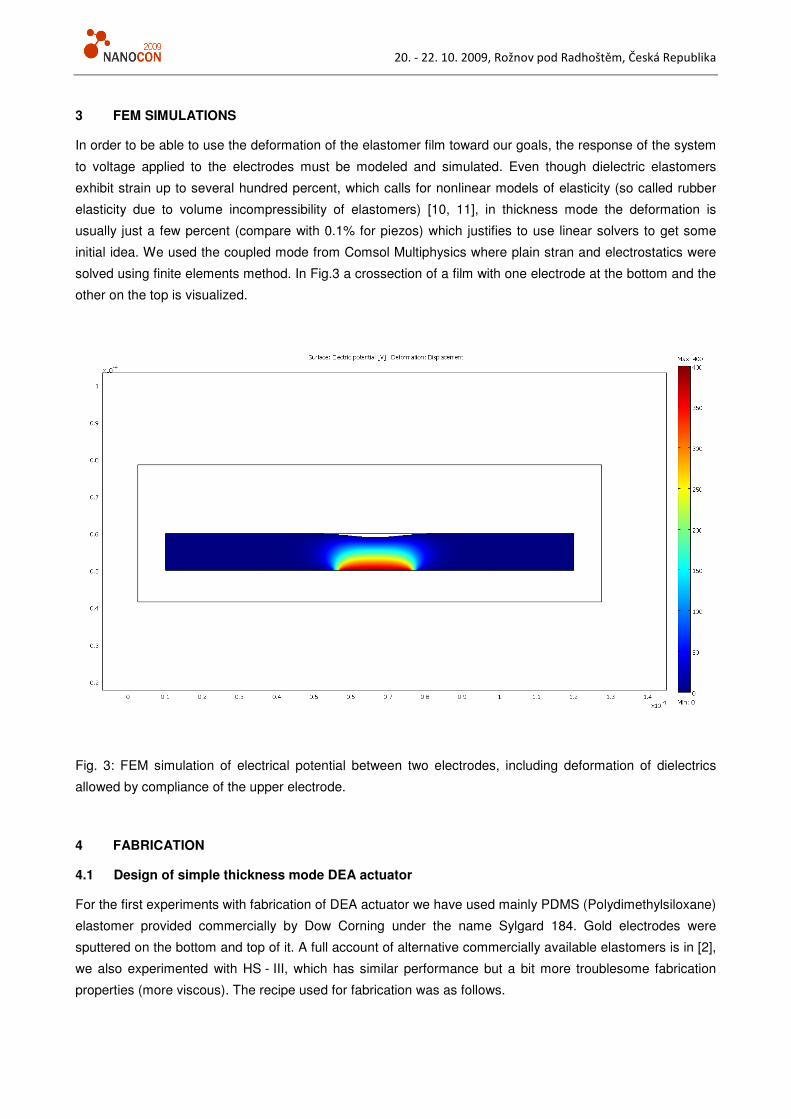
In order to be able to use the deformation of the elastomer film toward our goals, the response of the system
to voltage applied to the electrodes must be modeled and simulated. Even though dielectric elastomers
exhibit strain up to several hundred percent, which calls for nonlinear models of elasticity (so called rubber
elasticity due to volume incompressibility of elastomers) [10, 11], in thickness mode the deformation is
usually just a few percent (compare with 0.1% for piezos) which justifies to use linear solvers to get some
initial idea. We used the coupled mode from Comsol Multiphysics where plain stran and electrostatics were
solved using finite elements method. In Fig.3 a crossection of a film with one electrode at the bottom and the
other on the top is visualized.
Fig. 3: FEM simulation of electrical potential between two electrodes, including deformation of dielectrics
allowed by compliance of the upper electrode.
4 FABRICATION
4.1 Design of simple thickness mode DEA actuator
For the first experiments with fabrication of DEA actuator we have used mainly PDMS (Polydimethylsiloxane)
elastomer provided commercially by Dow Corning under the name Sylgard 184. Gold electrodes were
sputtered on the bottom and top of it. A full account of alternative commercially available elastomers is in [2],
we also experimented with HS - III, which has similar performance but a bit more troublesome fabrication
properties (more viscous). The recipe used for fabrication was as follows.
20. - 22. 10. 2009, Rožnov pod Radhoštěm, Česká Republika
On the glass substrate create gold electrodes by sputtering gold (possibly chromium first to improve
adhesion). Thickness of gold on substrate should be about 40 nm, which provides small enough resistance
even for electrodes a few tens of microns wide. The sputtered gold layer should not be much thicker
because roughness of substrate affects homogeneity of elastomer film very much. With the final gold of
measuring spatial deformation of the film, we fabricated very narrow electrodes, about 100 µm. This was
done by laser ablation using an eximer laser available in a lab or our research partner. Typical outcome is in
Fig.3. Next step is to create an elastomer film on top of this patterned gold electrode. The easiest way to
deposit a thin layer of PDMS (about 10 µm) is using a spincoater (iterating a bit on the right spinning profile).
The PDMS comes in two parts (base and curing agent) which must be mixed immediately before
spincoating, because the crosslinking process starts immediately. After spincoating, the sample is placed
into an oven for about 1 hour to finish the crosslinking process during which the elastomers becoms a solid
film (no longer flowing). Finally the top electrode needs to be deposited. We used the same process as with
the bottom (substrate) electrode using sputtering gold. The only difference is that now thickness of sputtered
gold matters a bit more, because it affects elasticity of the resulting system.
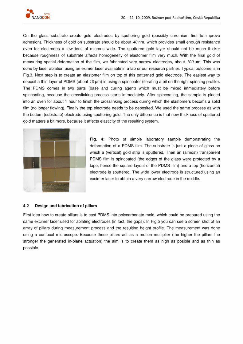
Fig. 4: Photo of simple laboratory sample demonstrating the
deformation of a PDMS film. The substrate is just a piece of glass on
which a (vertical) gold strip is sputtered. Then an (almost) transparent
PDMS film is spincoated (the edges of the glass were protected by a
tape, hence the square layout of the PDMS film) and a top (horizontal)
electrode is sputtered. The wide lower electrode is structured using an
excimer laser to obtain a very narrow electrode in the middle.
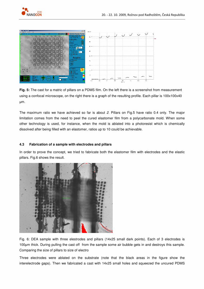
4.2 Design and fabrication of pillars
First idea how to create pillars is to cast PDMS into polycarbonate mold, which could be prepared using the
same excimer laser used for ablating electrodes (in fact, the gaps). In Fig.5 you can see a screen shot of an
array of pillars during measurement process and the resulting height profile. The measurement was done
using a confocal microscope. Because these pillars act as a motion multiplier (the higher the pillars the
stronger the generated in-plane actuation) the aim is to create them as high as posible and as thin as
possible.
20. - 22. 10. 2009, Rožnov pod Radhoštěm, Česká Republika
The maximum ratio we have achieved so far is about 2. Pillars on Fig.5 have ratio 0.4 only. The major
limitation comes from the need to peel the cured elastomer film from a polycarbonate mold. When some
other technology is used, for instance, when the mold is ablated into a photoresist which is chemically
dissolved after being filled with an elastomer, ratios up to 10 could be achievable.
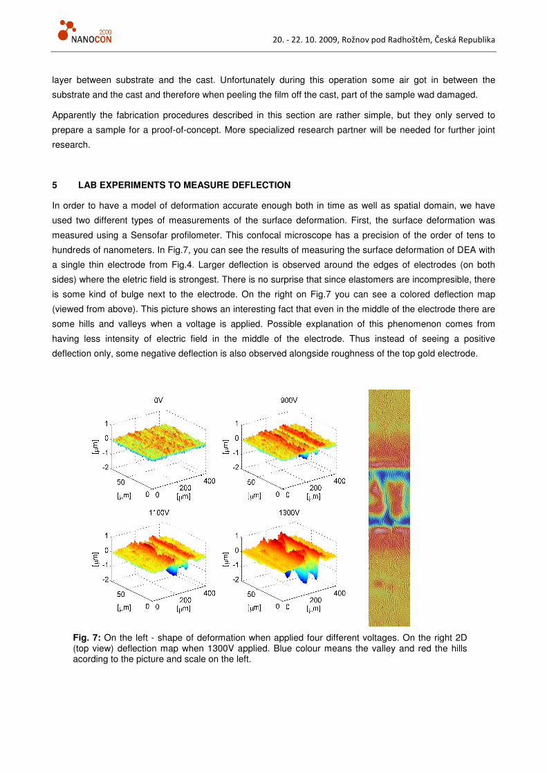
4.3 Fabrication of a sample with electrodes and pillars
In order to prove the concept, we tried to fabricate both the elastomer film with electrodes and the elastic
pillars. Fig.6 shows the result.
Fig. 6: DEA sample with three elestrodes and pillars (14x25 small dark points). Each of 3 electrodes is
100µm thick. During pulling the cast off from the sample some air bubble gets in and destroys this sample.
Comparing the size of pillars to size of electro
Three electrodes were ablated on the substrate (note that the black areas in the figure show the
interelectrode gaps). Then we fabricated a cast with 14x25 small holes and squeezed the uncured PDMS
Fig. 5: The cast for a matric of pillars on a PDMS film. On the left there is a screenshot from measurement
using a confocal microscope, on the right there is a graph of the resulting profile. Each pillar is 100x100x40
µm.
20. - 22. 10. 2009, Rožnov pod Radhoštěm, Česká Republika
layer between substrate and the cast. Unfortunately during this operation some air got in between the
substrate and the cast and therefore when peeling the film off the cast, part of the sample wad damaged.
Apparently the fabrication procedures described in this section are rather simple, but they only served to
prepare a sample for a proof-of-concept. More specialized research partner will be needed for further joint
research.
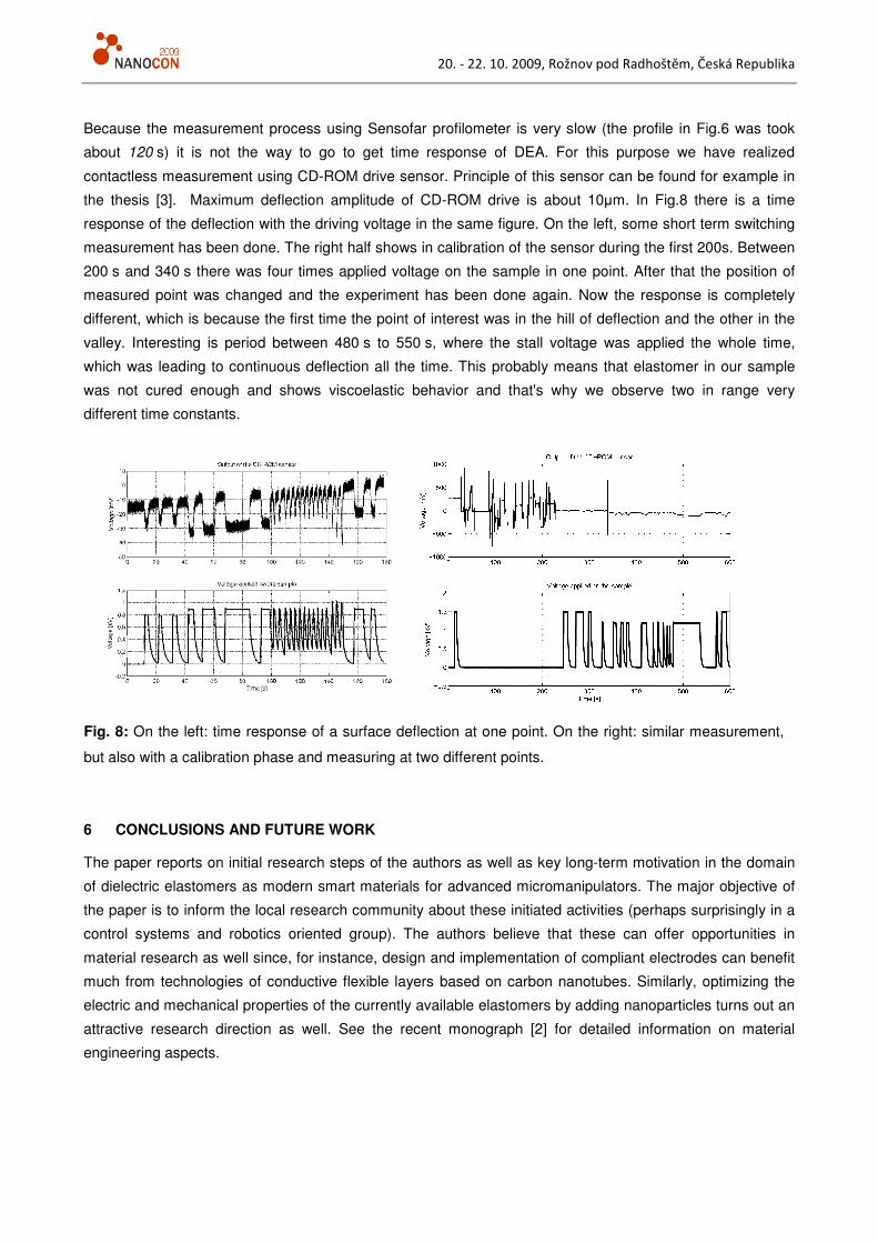
5 LAB EXPERIMENTS TO MEASURE DEFLECTION
In order to have a model of deformation accurate enough both in time as well as spatial domain, we have
used two different types of measurements of the surface deformation. First, the surface deformation was
measured using a Sensofar profilometer. This confocal microscope has a precision of the order of tens to
hundreds of nanometers. In Fig.7, you can see the results of measuring the surface deformation of DEA with
a single thin electrode from Fig.4. Larger deflection is observed around the edges of electrodes (on both
sides) where the eletric field is strongest. There is no surprise that since elastomers are incompresible, there
is some kind of bulge next to the electrode. On the right on Fig.7 you can see a colored deflection map
(viewed from above). This picture shows an interesting fact that even in the middle of the electrode there are
some hills and valleys when a voltage is applied. Possible explanation of this phenomenon comes from
having less intensity of electric field in the middle of the electrode. Thus instead of seeing a positive
deflection only, some negative deflection is also observed alongside roughness of the top gold electrode.
Fig. 7: On the left - shape of deformation when applied four different voltages. On the right 2D (top view) deflection map when 1300V applied. Blue colour means the valley and red the hills acording to the picture and scale on the left.
20. - 22. 10. 2009, Rožnov pod Radhoštěm, Česká Republika
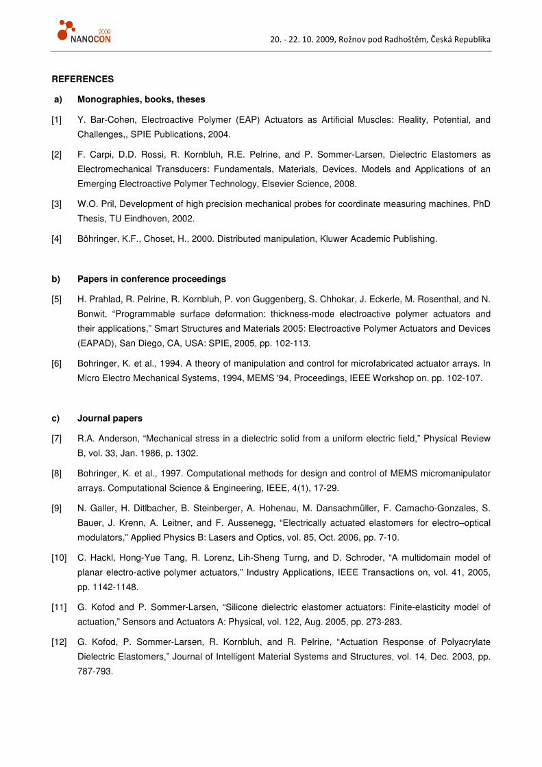
Because the measurement process using Sensofar profilometer is very slow (the profile in Fig.6 was took
about 120 s) it is not the way to go to get time response of DEA. For this purpose we have realized
contactless measurement using CD-ROM drive sensor. Principle of this sensor can be found for example in
the thesis [3]. Maximum deflection amplitude of CD-ROM drive is about 10µm. In Fig.8 there is a time
response of the deflection with the driving voltage in the same figure. On the left, some short term switching
measurement has been done. The right half shows in calibration of the sensor during the first 200s. Between
200 s and 340 s there was four times applied voltage on the sample in one point. After that the position of
measured point was changed and the experiment has been done again. Now the response is completely
different, which is because the first time the point of interest was in the hill of deflection and the other in the
valley. Interesting is period between 480 s to 550 s, where the stall voltage was applied the whole time,
which was leading to continuous deflection all the time. This probably means that elastomer in our sample
was not cured enough and shows viscoelastic behavior and that's why we observe two in range very
different time constants.
6 CONCLUSIONS AND FUTURE WORK
The paper reports on initial research steps of the authors as well as key long-term motivation in the domain
of dielectric elastomers as modern smart materials for advanced micromanipulators. The major objective of
the paper is to inform the local research community about these initiated activities (perhaps surprisingly in a
control systems and robotics oriented group). The authors believe that these can offer opportunities in
material research as well since, for instance, design and implementation of compliant electrodes can benefit
much from technologies of conductive flexible layers based on carbon nanotubes. Similarly, optimizing the
electric and mechanical properties of the currently available elastomers by adding nanoparticles turns out an
attractive research direction as well. See the recent monograph [2] for detailed information on material
engineering aspects.
Fig. 8: On the left: time response of a surface deflection at one point. On the right: similar measurement,
but also with a calibration phase and measuring at two different points.
20. - 22. 10. 2009, Rožnov pod Radhoštěm, Česká Republika
REFERENCES
a) Monographies, books, theses
[1] Y. Bar-Cohen, Electroactive Polymer (EAP) Actuators as Artificial Muscles: Reality, Potential, and
Challenges,, SPIE Publications, 2004.
[2] F. Carpi, D.D. Rossi, R. Kornbluh, R.E. Pelrine, and P. Sommer-Larsen, Dielectric Elastomers as
Electromechanical Transducers: Fundamentals, Materials, Devices, Models and Applications of an
Emerging Electroactive Polymer Technology, Elsevier Science, 2008.
[3] W.O. Pril, Development of high precision mechanical probes for coordinate measuring machines, PhD
Thesis, TU Eindhoven, 2002.
[4] Böhringer, K.F., Choset, H., 2000. Distributed manipulation, Kluwer Academic Publishing.
b) Papers in conference proceedings
[5] H. Prahlad, R. Pelrine, R. Kornbluh, P. von Guggenberg, S. Chhokar, J. Eckerle, M. Rosenthal, and N.
Bonwit, “Programmable surface deformation: thickness-mode electroactive polymer actuators and
their applications,” Smart Structures and Materials 2005: Electroactive Polymer Actuators and Devices
(EAPAD), San Diego, CA, USA: SPIE, 2005, pp. 102-113.
[6] Bohringer, K. et al., 1994. A theory of manipulation and control for microfabricated actuator arrays. In
Micro Electro Mechanical Systems, 1994, MEMS '94, Proceedings, IEEE Workshop on. pp. 102-107.
c) Journal papers
[7] R.A. Anderson, “Mechanical stress in a dielectric solid from a uniform electric field,” Physical Review
B, vol. 33, Jan. 1986, p. 1302.
[8] Bohringer, K. et al., 1997. Computational methods for design and control of MEMS micromanipulator
arrays. Computational Science & Engineering, IEEE, 4(1), 17-29.
[9] N. Galler, H. Ditlbacher, B. Steinberger, A. Hohenau, M. Dansachmüller, F. Camacho-Gonzales, S.
Bauer, J. Krenn, A. Leitner, and F. Aussenegg, “Electrically actuated elastomers for electro–optical
modulators,” Applied Physics B: Lasers and Optics, vol. 85, Oct. 2006, pp. 7-10.
[10] C. Hackl, Hong-Yue Tang, R. Lorenz, Lih-Sheng Turng, and D. Schroder, “A multidomain model of
planar electro-active polymer actuators,” Industry Applications, IEEE Transactions on, vol. 41, 2005,
pp. 1142-1148.
[11] G. Kofod and P. Sommer-Larsen, “Silicone dielectric elastomer actuators: Finite-elasticity model of
actuation,” Sensors and Actuators A: Physical, vol. 122, Aug. 2005, pp. 273-283.
[12] G. Kofod, P. Sommer-Larsen, R. Kornbluh, and R. Pelrine, “Actuation Response of Polyacrylate
Dielectric Elastomers,” Journal of Intelligent Material Systems and Structures, vol. 14, Dec. 2003, pp.
787-793.
20. - 22. 10. 2009, Rožnov pod Radhoštěm, Česká Republika
[13] H. Kück, W. Doleschal, A. Gehner, W. Grundke, R. Melcher, J. Paufler, R. Seltmann, and G. Zimmer,
“Deformable micromirror devices as phase-modulating high-resolution light valves,” Sensors and
Actuators A: Physical, vol. 54, Jun. 1996, pp. 536-541.
[14] Luntz, J.E., Messner, W. & Choset, H., 2001. Distributed Manipulation Using Discrete Actuator Arrays.
The International Journal of Robotics Research, 20(7), 553-583.
[15] Murphey, T.D. & Burdick, J.W., 2003. Feedback Control for Distributed Manipulation. In Algorithmic
Foundations of Robotics V. pp. 487-504.
[16] R. Pelrine, R. Kornbluh, Q. Pei, and J. Joseph, “High-Speed Electrically Actuated Elastomers with
Strain Greater Than 100%,” Science, vol. 287, Feb. 2000, pp. 836-839.
[17] S. Sakarya, G. Vdovin, and P.M. Sarro, “Spatial light modulators based on micromachined reflective
membranes on viscoelastic layers,” Sensors and Actuators A: Physical, vol. 108, Nov. 2003, pp. 271-
275.


![[Array, Array, Array, Array, Array, Array, Array, Array, Array, Array, Array, Array]](https://img.pdfslide.net/doc/110x75/56816460550346895dd63b8b/array-array-array-array-array-array-array-array-array-array-array.jpg)