Embed Size (px)
Citation preview

Audio
Source
And Control
RIGHT
LEFT
TPA3138D2
PLIMIT
MOD_SEL
SD/FAULT
Power Limit
Modulation Schemes/UV Level Select
PVCC/AVCCPower Supply
3.5V t 14.4V
FB
FB
GAIN_SEL 20dB/26dB GAIN Select
PBTL
DETECT
20.50 mm
20.7
5 m
m
Product
Folder
Order
Now
Technical
Documents
Tools &
Software
Support &Community
An IMPORTANT NOTICE at the end of this data sheet addresses availability, warranty, changes, use in safety-critical applications,intellectual property matters and other important disclaimers. PRODUCTION DATA.
TPA3138D2SLOS993A –MARCH 2018–REVISED JUNE 2018
TPA3138D2 10-W, 3.5-V to 14.4-V, Inductor Free, Stereo Class-D Speaker Amplifier
1
1 Features1• Wide Supply Range 3.5-V to 14.4-V
– 2 × 10 W into 6-Ω, 1% THD+N, 12-V Supply– 1 x 18.5 W into 4-Ω, 10% THD+N, 12-V Supply– THD+N : 0.04% at 1 W, 1 kHz input, 6-Ω
• Longer Battery Life for Portable Applications:– 20-mA (12-V) Idle Current in 1SPW Mode– >90% Class-D Efficiency
• Reduced Solution Size and Cost:– Inductor-Free Operation– EN55013 and EN55022 EMC Compliant When
No Inductors are Used– No External Heatsink Required
• Flexible Audio Solution:– Single-ended or Differential Analog Inputs– Selectable Gain: 20 dB and 26 dB– Pop and Click-Free Startup
• Integrated Protections and Auto Recovery:– Pin-to-pin, Pin-to-Ground, and Pin-to-Power
Short Circuit Protection– Thermal Protection, Undervoltage Protection,
and Overvoltage Protection– Power Limiter and DC Speaker Protection
• Pin-to-Pin Compatible with TPA3110D2,TPA3136D2 and TPA3136AD2
2 Applications• Televisions and Monitors• Bluetooth® Speakers and Wireless Speakers• Audio Amplifiers in Smart Appliance• Audio Speakers in Internet of Things• Consumer Audio Equipment
3 DescriptionThe TPA3138D2 is a 10-W/ch, high-efficiency, low-idle-current Class-D stereo audio amplifier. It candrive stereo speakers with a load as low as 3.2-Ω. Inthe 1SPW mode, it consumes a low idle current ofonly 21-mA (12-V) and can operate down to 3.5-V,allowing for longer audio play and improved thermalperformance in bluetooth speakers, battery-poweredappliances and other power-sensitive applications.
Advanced EMI Suppression with Spread SpectrumControl enables the use of inexpensive ferrite beadfilters while meeting EMC requirements for systemcost reduction.
To further simplify the design, the TPA3138D2integrates essential protection features includingundervoltage, overvoltage, power limit, short circuit,overtemperature, as well as DC speaker protection.All of these protections come with automaticrecovery.
Customers can leverage every TPA3138D2 feature inexisting designs as it is fully pin-to-pin compatible toTI's TPA3110D2, TPA3136D2 and TPA3136AD2.
Device Information(1)
PART NUMBER PACKAGE BODY SIZE (NOM)TPA3138D2 HTSSOP (28) 9.70 mm × 4.40 mm
(1) For all available packages, see the orderable addendum atthe end of the datasheet.
Simplified SchematicTPA3138 Layout with Ferrite Beads

2
TPA3138D2SLOS993A –MARCH 2018–REVISED JUNE 2018 www.ti.com
Product Folder Links: TPA3138D2
Submit Documentation Feedback Copyright © 2018, Texas Instruments Incorporated
Table of Contents1 Features .................................................................. 12 Applications ........................................................... 13 Description ............................................................. 14 Revision History..................................................... 25 Device Comparison Table ..................................... 36 Pin Configuration and Functions ......................... 37 Specifications......................................................... 5
7.1 Absolute Maximum Ratings ...................................... 57.2 ESD Ratings ............................................................ 57.3 Recommended Operating Conditions....................... 67.4 Thermal Information .................................................. 67.5 Electrical Characteristics........................................... 77.6 Switching Characteristics .......................................... 77.7 Typical Characteristics .............................................. 8
8 Parameter Measurement Information ................ 109 Detailed Description ............................................ 11
9.1 Overview ................................................................. 119.2 Functional Block Diagram ....................................... 129.3 Feature Description................................................. 13
9.4 Device Functional Modes........................................ 1610 Application and Implementation........................ 18
10.1 Application Information.......................................... 1810.2 Typical Applications ............................................. 18
11 Power Supply Recommendations ..................... 2511.1 Power Supply Decoupling, CS ............................. 25
12 Layout................................................................... 2612.1 Layout Guidelines ................................................. 2612.2 Layout Example .................................................... 27
13 Device and Documentation Support ................. 2813.1 Device Support .................................................... 2813.2 Documentation Support ....................................... 2813.3 Receiving Notification of Documentation Updates 2813.4 Community Resources.......................................... 2813.5 Trademarks ........................................................... 2813.6 Electrostatic Discharge Caution............................ 2813.7 Glossary ................................................................ 28
14 Mechanical, Packaging, and OrderableInformation ........................................................... 28
4 Revision HistoryNOTE: Page numbers for previous revisions may differ from page numbers in the current version.
Changes from Original (March 2018) to Revision A Page
• Changed the device status From: Advanced Information To: Production data ..................................................................... 1

1NC 28 PVCCL
2SD/FAULT 27 PVCCL
3LINP 26 BSPL
4LINN 25 OUTPL
5GAIN_SEL 24 GND
6MODE_SEL 23 OUTNL
7AVCC 22 BSNL
8GND 21 BSNR
9GVDD 20 OUTNR
10PLIMIT 19 GND
11RINN 18 OUTPR
12RINP 17 BSPR
13NC 16 PVCCR
14AGND 15 PVCCR
Not to scale
Thermal
Pad
3
TPA3138D2www.ti.com SLOS993A –MARCH 2018–REVISED JUNE 2018
Product Folder Links: TPA3138D2
Submit Documentation FeedbackCopyright © 2018, Texas Instruments Incorporated
5 Device Comparison Table
Product Supply Voltage Modulation Scheme Package Rdson Gain Inductor FreeTPA3138D2 3.5-V to 14.4-V BD, 1SPW HTSSOP-28 180-mΩ 20-dB, 26-dB YESTPA3110D2 8-V to 26-V BD HTSSOP-28 240-mΩ 20-dB, 26-dB, 32-dB, 36-dB NOTPA3136D2 4.5-V to 14.4-V BD HTSSOP-28 240-mΩ 26-dB YES
TPA3136AD2 8-V to 14.4-V BD HTSSOP-28 240-mΩ 26-dB YES
(1) I = Input, O = Output, IO = Input and Output, P = Power
6 Pin Configuration and Functions
PWP Package28-Pin HTSSOP
(Top View)
Pin FunctionsPIN
I/O/P (1) DESCRIPTIONNAME NO.NC 1 – No Connect Pin. Can be shorted to PVCC or shorted to GND or left open.
SD/FAULT 2 IO
TTL logic levels with compliance to AVCC. Shutdown logic input for audio amp (LOW , outputs Hi-Z;HIGH , outputs enabled). General fault reporting including Over-Temp, Over-Current, DC Detect.SD/FAULT= High, normal operation, SD/FAULT= Low, fault condition Device will auto-recover oncethe OT/OC/DC Fault has been removed.
LINP 3 I Positive audio input for left channel. Biased at 2.5 V. Connect to GND for PBTL mode.LINN 4 I Negative audio input for left channel. Biased at 2.5 V. Connect to GND for PBTL mode.
GAIN_SEL 5 I Gain select least significant bit. TTL logic levels with compliance to AVDD. Low = 20 dB Gain, High =26 dB Gain, Floating = 26 dB Gain.

4
TPA3138D2SLOS993A –MARCH 2018–REVISED JUNE 2018 www.ti.com
Product Folder Links: TPA3138D2
Submit Documentation Feedback Copyright © 2018, Texas Instruments Incorporated
Pin Functions (continued)PIN
I/O/P (1) DESCRIPTIONNAME NO.
MODE_SEL 6 IMode select least significant bit. TTL logic levels with compliance to AVDD. Low = BD Mode/UVThreshold = 7.5 V, High = Low-Idle-Current 1SPW Mode/UV Threshold = 3.4V, Floating = Low-Idle-Current 1SPW Mode/UV threshold = 3.4V
AVCC 7 P Analog supply.GND 8 – Analog signal ground.GVDD 9 O FET gate drive supply. Nominal voltage is 5 V.
PLIMIT 10 I Power limiter level control. Connect a resistor divider from GVDD to GND to set power limit. Connectdirectly to GVDD for no power limit.
RINN 11 I Negative audio input for right channel. Biased at 2.5 V.RINP 12 I Positive audio input for right channel. Biased at 2.5 V.NC 13 – No Connect Pin. Can be shorted to PVCC or shorted to GND or left open.AGND 14 – Analog signal ground. Connect to the thermal pad.
PVCCR 15, 16 P Power supply for right channel H-bridge. Right channel and left channel power supply inputs areconnected internally.
BSPR 17 P Bootstrap supply (BST) for right channel, positive high-side FET.OUTPR 18 O Class-D H-bridge positive output for right channel.GND 19 – Power ground for the H-bridges.OUTNR 20 O Class-D H-bridge negative output for right channel.BSNR 21 P Bootstrap supply (BST) for right channel, negative high-side FET.BSNL 22 P Bootstrap supply (BST) for left channel, negative high-side FET.OUTNL 23 O Class-D H-bridge negative output for left channel.GND 24 – Power ground for the H-bridges.OUTPL 25 O Class-D H-bridge positive output for left channel.BSPL 26 P Bootstrap supply (BST) for left channel, positive high-side FET.
PVCCL 27, 28 P Power supply for left channel H-bridge. Right channel and left channel power supply inputs areconnected internally.
Thermal Pad – Connect to GND for best thermal and electrical performance

5
TPA3138D2www.ti.com SLOS993A –MARCH 2018–REVISED JUNE 2018
Product Folder Links: TPA3138D2
Submit Documentation FeedbackCopyright © 2018, Texas Instruments Incorporated
(1) Stresses beyond those listed under Absolute Maximum Ratings may cause permanent damage to the device. These are stress ratingsonly, which do not imply functional operation of the device at these or any other conditions beyond those indicated under RecommendedOperating Conditions. Exposure to absolute-maximum-rated conditions for extended periods may affect device reliability.
(2) The voltage slew rate of these pins must be restricted to no more than 10 V/ms. For higher slew rates, use a 100 kΩ resister in serieswith the pins.
7 Specifications
7.1 Absolute Maximum Ratingsover operating free-air temperature range (unless otherwise noted) (1)
MIN MAX UNITSupply voltage AVCC to GND, PVCC to GND –0.3 20 VInput current To any pin except supply pins 10 mA
Interface pin voltageSD/FAULT to GND (2), GAIN_SEL, MODE_SEL
–0.3 AVCC + 0.3 V10 V/ms
PLIMIT -0.3 GVDD + 0.3 VRINN, RINP, LINN, LINP –0.3 5.5 V
Minimum load resistance, RL
BTL, (10 V < PVCC < 14.4 V) 4.8
ΩBTL, (3.5 V < PVCC < 10 V) 3.2PBTL, (10 V < PVCC < 14.4 V) 2.4PBTL, (3.5 V < PVCC < 10 V) 1.6
Continuous total power dissipation See the ThermalInformation Table
Operating Juncation Temperature range –25 150 °CStorage temperature range, Tstg –40 125 °C
(1) JEDEC document JEP155 states that 500-V HBM allows safe manufacturing with a standard ESD control process.(2) JEDEC document JEP157 states that 250-V CDM allows safe manufacturing with a standard ESD control process.
7.2 ESD RatingsVALUE UNIT
V(ESD) Electrostatic dischargeHuman body model (HBM), per ANSI/ESDA/JEDEC JS-001 (1) ±1000
VCharged device model (CDM), per JEDEC specification JESD22-C101 (2) ±250

6
TPA3138D2SLOS993A –MARCH 2018–REVISED JUNE 2018 www.ti.com
Product Folder Links: TPA3138D2
Submit Documentation Feedback Copyright © 2018, Texas Instruments Incorporated
(1) Set SD/FAULT to high level, make sure the pull-up resistor is larger than 4.7 kΩ and smaller than 500 kΩ(2) Set GAIN_SEL and MODE_SEL to low level, make sure pull down resistor<10kΩ(3) The TPA3138D2 incorporates an exposed thermal pad on the underside of the chip. This acts as a heatsink, and it must be connected
to a thermally dissipating plane for proper power dissipation. Failure to do so may result in the device going into thermal protectionshutdown. See TI Technical Briefs SLMA002 for more information about using the TSSOP thermal pad.
7.3 Recommended Operating Conditionsover operating free-air temperature range (unless otherwise noted)
PARAMETER TEST CONDITIONS MIN MAX UNITVCC Supply voltage PVCC, AVCC 3.5 14.4 VVIH High-level input voltage SD/FAULT (1), GAIN_SEL, MODE_SEL 2 AVCC VVIL Low-level input voltage SD/FAULT, GAIN_SEL, MODE_SEL (2) 0.8 VVOL Low-level output voltage SD/FAULT, RPULL-UP =100 kΩ, PVCC = 14.4 V 0.8 VIIH High-level input current SD/FAULT, GAIN_SEL, MODE_SEL, VI = 2 V, AVCC = 12 V 50 µA
IIL Low-level input current SD/FAULT, GAIN_SEL, MODE_SEL, VI = 0.8 V, AVCC = 12V 5 µA
TA Operating free-air temperature (3) –10 85 °CTJ Operating junction temperature (3) -10 150 °C
(1) For more information about traditional and new thermal metrics, see the IC Package Thermal Metrics application report, SPRA953.
7.4 Thermal Information
THERMAL METRIC (1)TPA3138D2
UNITPWP (HTSSOP)28 PINS
RθJA Junction-to-ambient thermal resistance 30.3 °C/WRθJC(top) Junction-to-case (top) thermal resistance 33.5 °C/WRθJB Junction-to-board thermal resistance 17.5 °C/WψJT Junction-to-top characterization parameter 0.9 °C/WψJB Junction-to-board characterization parameter 7.2 °C/WRθJC(bot) Junction-to-case (bottom) thermal resistance 0.9 °C/W

7
TPA3138D2www.ti.com SLOS993A –MARCH 2018–REVISED JUNE 2018
Product Folder Links: TPA3138D2
Submit Documentation FeedbackCopyright © 2018, Texas Instruments Incorporated
7.5 Electrical CharacteristicsTA = 25°C, AVCC = PVCC = 12 V, RL = 6 Ω. Over operating free-air temperature range (unless otherwise noted)
PARAMETER TEST CONDITIONS MIN TYP MAX UNIT
AC CHARACTERISTICS
PSRR Power supply ripple rejection 200-mVPP ripple at 1 kHz,Gain = 26 dB, Inputs ac-coupled to GND –70 dB
PO Continuous output power, BTL THD+N = 1%, f = 1 kHz, PVCC = 12 V, RL = 6 Ω 10 W
PO Continuous output power, BTL THD+N = 10%, f = 1 kHz, PVCC = 12 V, RL = 6 Ω 12 W
PO Continuous output power, BTL THD+N = 1%, f = 1 kHz, PVCC = 12 V, RL = 8 Ω 8 W
PO Continuous output power, BTL THD+N = 10%, f = 1 kHz, PVCC = 12 V, RL = 8 Ω 9.9 W
PO Continuous output power, PBTL (mono) THD+N = 10%, f = 1 kHz, PVCC = 12 V, RL = 4 Ω 18.5 W
IO Maximum output current f = 1 kHz, RL = 3 Ω 3.5 A
THD+N Total harmonic distortion + noise f = 1 kHz, PO = 5 W (half-power) 0.04 %
Vn Output integrated noise
20 Hz to 22 kHz, A-weighted filter, Gain = 26 dB85 µV
–81 dBV
20 Hz to 22 kHz, A-weighted filter, Gain = 20 dB72 µV
-82.6 dBV
Crosstalk VO = 1 Vrms, Gain = 26 dB, f = 1 kHz -95 dB
SNR Signal-to-noise ratio Maximum output at THD+N < 1%,f = 1 kHz, Gain = 26 dB, A-weighted 102 dB
OTE Thermal trip point 150 °C
Thermal hysteresis 15 °C
DC CHARACTERISTICS
| VOS | Output offset voltage(measured differentially) VI = 0 V, Gain = 26 dB 1.5 mV
ICC Quiescent supply current SD/FAULT = 2 V, 10 µF + 680 nF output filter,1SPW Mode, PVCC = 12 V 20 mA
ICC Quiescent supply current SD/FAULT = 2 V, 10 µF + 680 nF output filter,BD Mode, PVCC = 12 V 37 mA
ICC(SD) Quiescent supply current in shutdown mode SD/FAULT = 0.8 V, no load 10 µA
rDS(on) Drain-source on-state resistanceIO = 500 mA, TJ = 25°Cexcluding metal andbond wire resistance
High Side 180mΩ
Low side 180
G Gain GAIN_SEL= 0.8 V 19 20 21 dB
G Gain GAIN_SEL= 2 V 25 26 27 dB
tON Turn-on time SD/FAULT = 2 V 50 ms
tOFF Turn-off time SD/FAULT = 0.8 V 2.9 µs
GVDD Gate drive supply IGVDD = 2 mA 4.8 5 5.2 V
tDCDET DC detect time VRINP = 2.6 V and VRINN = 2.4 V,or VRINP = 2.4 V and VRINN = 2.6 V 800 ms
OVP Over Voltage Protection 15.8 V
UVP Under Voltage Protection MODE_SEL = 0.8 V (BD mode) 7.5 V
UVP Under Voltage Protection MODE_SEL = 2 V, or floating (1SPW mode) 3.4 V
7.6 Switching Characteristicsover operating free-air temperature range (unless otherwise noted)
PARAMETER MIN NOM MAX UNITfOSC, SS Oscillator frequency, Spread Spectrum ON 305 340 kHz

Supply Voltage (V)
Out
put P
ower
(W
)
7 8 9 10 11 12 13 14 15 160
2
4
6
8
10
12
14
16
18
20
10
D005D005
THD+N=1%THD+N=10%
Supply Voltage (V)
Out
put P
ower
(W
)
7 8 9 10 11 12 13 14 15 160
2
4
6
8
10
12
14
16
18
20
10
D006D006
THD+N=1%THD+N=10%
Output Power (W)
TH
D+N
(%
)
0.01
0.020.030.05
0.1
0.20.30.5
1
235
10
0.01 0.1 1 10
D003D003
f= 20Hzf= 1kHz
Output Power (W)
TH
D+N
(%
)
0.01
0.020.030.05
0.1
0.20.30.5
1
235
10
0.01 0.1 1 10
D004D004
f= 20Hzf= 1kHz
Frequency (Hz)
TH
D+
N (
%)
0.001
0.01
0.1
1
10
100 1k 10k20 20k
D001D001
P O=1WPO =2.5WPO=5W
Frequency (Hz)
TH
D+
N (
%)
0.001
0.01
0.1
1
10
100 1k 10k20 20k
D004D001D002
P O=1WPO =2.5WPO=5W
8
TPA3138D2SLOS993A –MARCH 2018–REVISED JUNE 2018 www.ti.com
Product Folder Links: TPA3138D2
Submit Documentation Feedback Copyright © 2018, Texas Instruments Incorporated
7.7 Typical CharacteristicsAll measurements taken at audio frequency = 1 kHz, closed-loop gain = 26 dB, BD mode, T A= 25°C, AES17 filter using theTPA3138D2EVM, unless otherwise noted.
AVCC=PVCC = 12 V, Load = 6 Ω + 47 µH, 1 W, 2.5 W, 5 W
Figure 1. THD+N vs Frequency (BTL)
AVCC=PVCC = 13 V, Load = 8 Ω + 66 µH, 1 W, 2.5 W, 5 W
Figure 2. THD+N vs Frequency (BTL)
AVCC=PVCC = 12 V, Load = 6 Ω + 47 µH, 20 Hz, 1 kHz
Figure 3. THD+N vs Output Power (BTL)
AVCC=PVCC = 13 V, Load = 8 Ω + 66 µH, 20 Hz, 1 kHz
Figure 4. THD+N + Noise vs Output Power (BTL)
AVCC=PVCC = 7.5 V to 15 V, Load = 6 Ω + 47 µH
Figure 5. Output Power vs Supply Voltage (BTL)
AVCC=PVCC = 7.5 V to 15 V, Load = 8 Ω + 66 µH
Figure 6. Output Power vs Supply Voltage (BTL)

f - Frequency - Hz
Cro
ssta
lk -
dB
r
-120
-100
-80
-60
-40
-20
0
10k 20k1k10020
D010D010
CH2 to CH1CH1 to CH2
Two Channel Total Output Power (W)
Pow
er E
ffici
ency
(%
)
0
10
20
30
40
50
60
70
80
90
100
0 5 10 15 20 25 30 35 40D009D009
PVCC = 13VPVCC = 14.4 V
Frequency (Hz)
Gai
n (d
B)
Pha
se (q)
0 -125
4 -75
8 -25
12 25
16 75
20 125
24 175
28 225
32 275
36 325
100 1k 10k20 20k
D007D007
GainPhase
Two Channel Total Output Power (W)
Pow
er E
ffici
ency
(%
)
0
10
20
30
40
50
60
70
80
90
100
0 5 10 15 20 25 30 35 40D008D008
PVCC = 13VPVCC = 14.4 V
Supply Voltage (V)
Out
put P
ower
(W
)
3 4 5 6 7 8 9 10 11 12 13 14 15 160
2
4
6
8
10
12
14
16
18
20
10
D019D019
THD+N=1%THD+N=10%
Supply Voltage (V)
Out
put P
ower
(W
)
3 4 5 6 7 8 9 10 11 12 13 14 15 160
2
4
6
8
10
12
14
16
18
10
D018D018
THD+N=1%THD+N=10%
9
TPA3138D2www.ti.com SLOS993A –MARCH 2018–REVISED JUNE 2018
Product Folder Links: TPA3138D2
Submit Documentation FeedbackCopyright © 2018, Texas Instruments Incorporated
Typical Characteristics (continued)All measurements taken at audio frequency = 1 kHz, closed-loop gain = 26 dB, BD mode, T A= 25°C, AES17 filter using theTPA3138D2EVM, unless otherwise noted.
AVCC=PVCC = 3.5 V to 15 V, Load = 6 Ω + 47 µH, Low-Idle-Current 1SPW Mode
Figure 7. Output Power vs Supply Voltage (BTL)
AVCC= PVCC = 3.5 V to 15 V, Load = 8 Ω + 66 µH, Low-Idle-Current 1SPW Mode
Figure 8. Output Power vs Supply Voltage (BTL)
AVCC= PVCC = 12 V, Load = 6 Ω + 47 µH
Figure 9. Gain and Phase vs Frequency (BTL)
AVCC=PVCC = 12 V, 14.4 V, Load = 6 Ω + 47 µH
Figure 10. Efficiency vs Output Power (BTL)
AVCC=PVCC= 13 V, 14.4 V, Load = 8 Ω + 66 µH
Figure 11. Efficiency vs Output Power (BTL)
AVCC=PVCC = 12 V, 1 W, Load = 6 Ω + 47 µH
Figure 12. Crosstalk vs Frequency (BTL)

Supply Voltage (V)
Out
put P
ower
(W
)
7 8 9 10 11 12 13 14 15 1602468
101214161820222426283032
10
D013D013
THD+N=1%THD+N=10%
Total Output Power (W)
Pow
er E
ffici
ency
(%
)
0
10
20
30
40
50
60
70
80
90
100
0 5 10 15 20 25 30 35 40
D014D014
PVCC = 12VPVCC = 14.4 V
f - Frequency - Hz
TH
D+
N -
Tot
al H
arm
onic
Dis
tort
ion
+ N
oise
- %
0.001
0.01
0.1
1
10
20 20k100 1k 10k
D012D012
1W2.5W5W
Po - Output Power - W
TH
D+
N -
Tot
al H
arm
onic
Dis
tort
ion
+ N
oise
- %
0.01
0.1
1
10
10m 100m 1 10 30
D013D013
20 Hz1 kHz
10
TPA3138D2SLOS993A –MARCH 2018–REVISED JUNE 2018 www.ti.com
Product Folder Links: TPA3138D2
Submit Documentation Feedback Copyright © 2018, Texas Instruments Incorporated
Typical Characteristics (continued)All measurements taken at audio frequency = 1 kHz, closed-loop gain = 26 dB, BD mode, T A= 25°C, AES17 filter using theTPA3138D2EVM, unless otherwise noted.
AVCC=PVCC = 13 V, Load = 4 Ω + 33 µH, 1 W, 2.5 W, 5 W
Figure 13. THD+N vs Frequency (PBTL)
AVCC=PVCC = 13 V, Load = 4 Ω + 33 µH, 20 Hz, 1 kHz
Figure 14. THD+N vs Output Power (PBTL)
AVCC=PVCC = 7.5 V to 14.4 V, Load = 4 Ω + 33 µH
Figure 15. Output Power vs Supply Voltage (PBTL)
AVCC=PVCC = 13 V, 14.4 V, Load = 4 Ω + 33 µH
Figure 16. Efficiency vs Output Power (PBTL)
8 Parameter Measurement InformationAll parameters are measured according to the conditions described in the Specifications section.
Most audio analyzers does not give correct readings of Class-D amplifiers’ performance due to their sensitivity tothe out-of-band noise present at the amplifier outputs. An AES-17 pre-analyzer filter is recommended to use forClass-D amplifier measurements. In absence of such filters, a 30-kHz low-pass filter (10 Ω + 47 nF) can be usedto reduce the out-of-band noise remaining on the amplifier outputs.

11
TPA3138D2www.ti.com SLOS993A –MARCH 2018–REVISED JUNE 2018
Product Folder Links: TPA3138D2
Submit Documentation FeedbackCopyright © 2018, Texas Instruments Incorporated
9 Detailed Description
9.1 OverviewThe TPA3138D2 is designed as a low-idle-power, cost-effective, general-purpose Class-D audio amplifier. Thebuilt-in spread spectrum control efficiently reduces EMI and enables the use of the ferrite beads instead of theinductors for ≤2x10W applications.
To facilitate system design, the TPA3138D2 needs only a single power supply between 3.5 V and 14.4 V foroperation. An internal voltage regulator provides suitable voltage levels for the gate driver, digital, and low-voltage analog circuitry. Additionally, all circuitry requiring a floating voltage supply, as in the high-side gate drive,is accommodated by built-in bootstrap circuitry with integrated boot strap diodes requiring only an externalcapacitor for each half-bridge.
The audio signal path, including the gate drive and output stage, is designed as identical, independent full-bridges. All decoupling capacitors should be placed as close as possible to their associated pins. The physicalloop with the power supply pins, decoupling capacitors, and GND return path to the device pins must be kept asshort as possible, and with as little area as possible to minimize induction (see reference board documentationfor additional information).
For a properly functioning bootstrap circuit, a small ceramic capacitor must be connected from each bootstrap pin(BSXX) to the power-stage output pin (OUTXX). When the power-stage output is low, the bootstrap capacitor ischarged through an internal diode connected between the gate-drive power-supply pin (GVDD) and the bootstrappins. When the power-stage output is high, the bootstrap capacitor potential is shifted above the output potentialand thus provides a suitable voltage supply for the high-side gate driver. In an application with PWM switchingfrequencies in the datasheet specified range, use ceramic capacitors with at least 220-nF capacitance, size 0603or 0805, for the bootstrap supply. These capacitors ensure sufficient energy storage, even during clipped lowfrequency audio signals, to keep the high-side power stage FET (LDMOS) fully turned on during the remainingpart of its ON cycle.
Special attention should be paid to the power-stage power supply; this includes component selection, PCBplacement, and routing. For optimal electrical performance, EMI compliance, and system reliability, each PVCCpin should be decoupled with ceramic capacitors that are placed as close as possible to each supply pin. It isrecommended to follow the PCB layout of the reference design. For additional information on recommendedpower supply and required components, see the application diagrams in this data sheet.
The PVCC power supply should have low output impedance and low noise. The power-supply ramp andSD/FAULT release sequence is not critical for device reliability as facilitated by the internal power-on-resetcircuit, but it is recommended to release SD/FAULT after the power supply is settled for minimum turn on audibleartifacts.

PWM
Logic
Gate
Drive
Gate
Drive
PVCC
PVCC
GVDD
PVCC
PVCC
BSPL
GND
OUTPL
OUTNL
GND
GVDD
BSNL
PWM
Logic
Gate
Drive
Gate
Drive
PVCC
PVCC
GVDD
PVCC
PVCC
BSNR
GND
OUTNR
OUTPR
GND
GVDD
BSPR
LINN
LINP
RINP
RINN
UVLO/OVLO
SC Detect
DC Detect
Thermal
Detect
Startup Protection
Logic
Biases and
References
SD/FAULT
SD
GAIN_SEL
MOD_SEL
AVCC
TTL
BufferRamp
Generator
AVDD
GVDD
GVDD
LDO
Regulator
Gain
Control PLIMIT
Spread Spectrum
Control
Gain
Control
Modulation Scheme
and PBTL Select
Modulation Scheme
and PBTL Select
OUTNL FB
OUTPL FB
OUTPR FB
OUTNR FB
OUTPR FB
OUTNR FB
OUTNL FB
OUTPL FB
PLIMIT
PLIMIT LIMITER
Reference
UVLO Select
FAULT
Gain
Control
Modulation scheme
/UVLO Select
Input
SensePBTL
Select
GND
12
TPA3138D2SLOS993A –MARCH 2018–REVISED JUNE 2018 www.ti.com
Product Folder Links: TPA3138D2
Submit Documentation Feedback Copyright © 2018, Texas Instruments Incorporated
9.2 Functional Block Diagram
13
TPA3138D2www.ti.com SLOS993A –MARCH 2018–REVISED JUNE 2018
Product Folder Links: TPA3138D2
Submit Documentation FeedbackCopyright © 2018, Texas Instruments Incorporated
9.3 Feature Description
9.3.1 Analog GainThe analog gain of the TPA3138D2 can be changed by GAIN_SEL pin. Low Level, Gain = 20 dB; High Level,Gain = 26 dB.
9.3.2 SD/FAULT OperationThe TPA3138D2 device employs a shutdown mode of operation designed to reduce supply current (ICC) to theabsolute minimum level during periods of nonuse for power conservation. The SD/FAULT input pin should beheld high (see Specifications table for trip point) during normal operation when the amplifier is in use. PullingSD/FAULT low causes the outputs to mute and the amplifier to enter a low-current state. Never leave SD/FAULTunconnected, because the amplifier operation would be unpredictable.
For the best power-off pop performance, place the amplifier in the shutdown mode prior to removing the powersupply voltage.
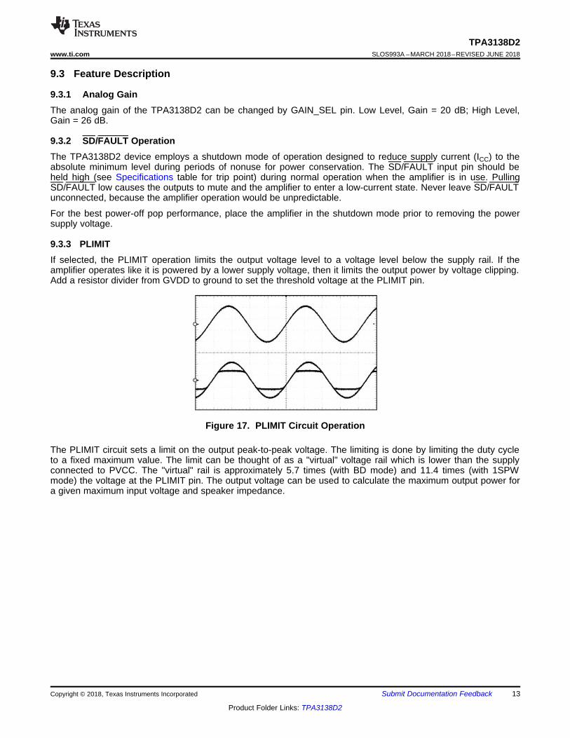
9.3.3 PLIMITIf selected, the PLIMIT operation limits the output voltage level to a voltage level below the supply rail. If theamplifier operates like it is powered by a lower supply voltage, then it limits the output power by voltage clipping.Add a resistor divider from GVDD to ground to set the threshold voltage at the PLIMIT pin.
Figure 17. PLIMIT Circuit Operation
The PLIMIT circuit sets a limit on the output peak-to-peak voltage. The limiting is done by limiting the duty cycleto a fixed maximum value. The limit can be thought of as a "virtual" voltage rail which is lower than the supplyconnected to PVCC. The "virtual" rail is approximately 5.7 times (with BD mode) and 11.4 times (with 1SPWmode) the voltage at the PLIMIT pin. The output voltage can be used to calculate the maximum output power fora given maximum input voltage and speaker impedance.

2
LP
L SOUT
L
RV
R + 2 RP = for unclipped power
2 R
æ öæ ö´ç ÷ç ÷ç ÷´è øè ø
´
14
TPA3138D2SLOS993A –MARCH 2018–REVISED JUNE 2018 www.ti.com
Product Folder Links: TPA3138D2
Submit Documentation Feedback Copyright © 2018, Texas Instruments Incorporated
Feature Description (continued)
where• POUT (10%THD) = 1.25 × POUT (unclipped)• RL is the load resistance.• RS is the total series resistance including RDS(on), and output filter resistance.• VP is the peak amplitude, which is limited by "virtual" voltage rail. (1)
9.3.4 Spread Spectrum and De-Phase ControlThe TPA3138D2 device has built-in spread spectrum control of the oscillator frequency and de-phase of thePWM outputs to improve EMI performance. The spread spectrum scheme is internally fixed and is always turnedon.
De-phase inverts the phase of the output PWM such that the idle output PWM waveforms of the two audiochannels are inverted. De-phase does not affect the audio signal, or its polarity. De-phase only works with BDmode, it is auto-disabled in 1SPW mode
9.3.5 GVDD SupplyThe GVDD Supply is used to power the gates of the output full-bridge transistors. Add a 1-μF capacitor to groundat this pin.
9.3.6 DC DetectThe TPA3138D2 device integrates a circuitry which protects the speakers from DC current that might occur dueto defective capacitors on the input or shorts on the printed circuit board at the inputs. A DC detect fault isreported on the SD/FAULT pin as a low state. The DC Detect fault also causes the amplifier to shutdown bychanging the state of the outputs to Hi-Z.
A DC Detect Fault is issued when the output DC voltage sustain for more than 800 msec at the same polarity.This feature protects the speaker from large DC currents or AC currents less than 1 Hz. To avoid nuisance faultsdue to the DC detect circuit, hold the SD/FAULT pin low at power-up until the signals at the inputs are stable.Also, take care to match the impedance seen at the positive and negative inputs to avoid nuisance DC detectfaults.
9.3.7 PBTL SelectThe TPA3138D2 device offers the feature of Parallel BTL operation with two outputs of each channel connecteddirectly. Connecting LINP and LINN directly to Ground (without capacitors) sets the device in Mono Mode duringpower up. Connect the OUTPR and OUTNR together for the positive speaker terminal and OUTNL and OUTPLtogether for the negative speaker terminal. Analog input signal is applied to INPR and INNR. For an example ofthe PBTL connection, see the schematic in the Typical Applications section.
9.3.8 Short-Circuit Protection and Automatic Recovery FeatureThe TPA3138D2 features over-current conditions against the output stage short-circuit conditions. The short-circuit protection fault is reported on the SD/FAULT pin as a low state. The amplifier outputs are switched to a Hi-Z state when the short circuit protection latch is triggered .
The device recovers automatically once the over-current condition has been removed.
9.3.9 Over-Temperature Protection (OTP)Thermal protection on the TPA3138D2 device prevents damage to the device when the internal die temperatureexceeds 150°C. This triggering point has a ±15°C tolerance from device to device. Once the die temperatureexceeds the thermal triggering point, the device is switched to the shutdown state and the outputs are disabled.
Thermal protection faults are reported on the SD/FAULT pin.

15
TPA3138D2www.ti.com SLOS993A –MARCH 2018–REVISED JUNE 2018
Product Folder Links: TPA3138D2
Submit Documentation FeedbackCopyright © 2018, Texas Instruments Incorporated
Feature Description (continued)The device recovers automatically once the over temperature condition has been removed.
9.3.10 Over-Voltage Protection (OVP)The TPA3138D2 device monitors the voltage on PVCC voltage threshold. When the voltage on PVCCL pin andPVCCR pin exceeds the over-voltage threshold (15.8 V typ), the OVP circuit puts the device into shutdownmode.
The device recovers automatically once the over-voltage condition has been removed.
9.3.11 Under-Voltage Protection (UVP)When the voltage on PVCCL pin and PVCCR pin falls below the under-voltage threshold, the UVP circuit putsthe device into shutdown mode. When MODE_SEL pin is set to LOW (BD mode), the under-voltage threshold is7.5 V typical. When MODE_SEL pin is set to HIGH or floating, the TPA3138D2 operates in 1SPW mode, and theunder-voltage threshold is 3.4 V typical.
The device recovers automatically once the under-voltage condition has been removed.

OUTP
OUTN
OUTP-OUTN
Speaker
Current
OUTP
OUTN
OUTP-OUTN
Speaker
Current
OUTP
OUTN
OUTP-OUTN
Speaker
Current
0V
0V
PVCC
No Output
Positive Output
Negative Output
0A
0A
0V
-PVCC
16
TPA3138D2SLOS993A –MARCH 2018–REVISED JUNE 2018 www.ti.com
Product Folder Links: TPA3138D2
Submit Documentation Feedback Copyright © 2018, Texas Instruments Incorporated
9.4 Device Functional Modes
9.4.1 MODE_SEL = LOW: BD ModulationThis is a modulation scheme that allows operation without the classic LC reconstruction filter when the amp isdriving an inductive load with short speaker wires. Each output is switching from 0 volts to the supply voltage.The OUTPx and OUTNx are in phase with each other with no input so that there is little or no current in thespeaker. The duty cycle of OUTPx is greater than 50% and OUTNx is less than 50% for positive output voltages.The duty cycle of OUTPx is less than 50% and OUTNx is greater than 50% for negative output voltages. Thevoltage across the load sits at 0 V throughout most of the switching period, reducing the switching current, whichreduces any I2R losses in the load.
Figure 18. BD Mode Modulation

OUTP
OUTN
OUTP-OUTN
Speaker
Current
OUTP
OUTN
OUTP-OUTN
Speaker
Current
OUTP
OUTN
OUTP-OUTN
Speaker
Current
0 V
0 V
PVCC
No Output
Positive Output
Negative Output
0 A
0 A
0 V
-PVCC
17
TPA3138D2www.ti.com SLOS993A –MARCH 2018–REVISED JUNE 2018
Product Folder Links: TPA3138D2
Submit Documentation FeedbackCopyright © 2018, Texas Instruments Incorporated
Device Functional Modes (continued)9.4.2 MODE_SEL = HIGH: Low-Idle-Current 1SPW ModulationThe 1SPW mode alters the normal modulation scheme in order to achieve higher efficiency with a slight penaltyin THD degradation and more attention required in the output filter selection. In 1SPW mode the outputs operateat ~15% modulation during idle conditions. When an audio signal is applied one output decreases and the otheroutput increases. The decreasing output signal rails to GND. At which point all the audio modulation takes placethrough the rising output. The result is that only one output is switching during a majority of the audio cycle.Efficiency is improved in this mode due to the reduction of switching losses.
Figure 19. Low-Idle-Current 1SPW Modulation

6
18
TPA3138D2SLOS993A –MARCH 2018–REVISED JUNE 2018 www.ti.com
Product Folder Links: TPA3138D2
Submit Documentation Feedback Copyright © 2018, Texas Instruments Incorporated
10 Application and Implementation
NOTEInformation in the following applications sections is not part of the TI componentspecification, and TI does not warrant its accuracy or completeness. TI’s customers areresponsible for determining suitability of components for their purposes. Customers shouldvalidate and test their design implementation to confirm system functionality.
10.1 Application InformationThe TPA3138D2 device is designed for use in inductor-free applications with limited distance wire lengthbetween amplifier and speakers, suitable for applications such as TV sets, sound docks and Bluetooth speakers.The TPA3138D2 device can either be configured in stereo or mono mode. Depending on the output powerrequirements and necessity for (speaker) load protection, the built-in PLIMIT circuit can be used to control thesystem power, see functional description of these features.
10.2 Typical Applications
Figure 20. Stereo Class-D Amplifier in BTL Configuration with Single-Ended Inputs, Spread SpectrumModulation and BD Mode

19
TPA3138D2www.ti.com SLOS993A –MARCH 2018–REVISED JUNE 2018
Product Folder Links: TPA3138D2
Submit Documentation FeedbackCopyright © 2018, Texas Instruments Incorporated
Typical Applications (continued)
Figure 21. Stereo Class-D Amplifier in PBTL Configuration with Single-Ended Input, Spread SpectrumModulation and 1SPW Mode
10.2.1 Design Requirements
10.2.1.1 PCB Material RecommendationFR-4 Glass Epoxy material with 1 oz. (35 µm) is recommended for use with the TPA3138D2. The use of thismaterial can provide higher power output, improved thermal performance, and better EMI margin (due to lowerPCB trace inductance). It is recommended to use several GND underneath the device thermal pad for thermalcoupling to a bottom-side copper GND plane for best thermal performance.
10.2.1.2 PVCC Capacitor RecommendationThe large capacitors used in conjunction with each full-bridge, are referred to as the PVCC capacitors. Thesecapacitors should be selected for proper voltage margin and adequate capacitance to support the powerrequirements. In practice, with a well designed system power supply, a capacitor with 100 μF and 16 V supportsmost applications with 12-V power supply. 25-V capacitor rating is recommended for power supply voltage higherthan 12 V. For The PVCC capacitors should be low ESR type because they are used in a circuit associated withhigh-speed switching.

20
TPA3138D2SLOS993A –MARCH 2018–REVISED JUNE 2018 www.ti.com
Product Folder Links: TPA3138D2
Submit Documentation Feedback Copyright © 2018, Texas Instruments Incorporated
Typical Applications (continued)10.2.1.3 Decoupling Capacitor RecommendationsIn order to design an amplifier that has robust performance, passes regulatory requirements, and exhibits goodaudio performance, good quality decoupling capacitors should be used. In practice, X7R should be used in thisapplication.
The voltage of the decoupling capacitors should be selected in accordance with good design practices.Temperature, ripple current, and voltage overshoot must be considered. This fact is particularly true in theselection of the ceramic capacitors that are placed on the power supply to each full-bridge. They must withstandthe voltage overshoot of the PWM switching, the heat generated by the amplifier during high power output, andthe ripple current created by high power output. A minimum voltage rating of 16 V is required for use with a 12-Vpower supply.
10.2.2 Detailed Design ProcedureA rising-edge transition on SD/FAULT input allows the device to start switching. It is recommended to ramp thePVCC voltage to its desired value before releasing SD/FAULT for minimum audible artifacts.
The device is not inverting the audio signal from input to output.
The GVDD pin is not recommended to be used as a voltage source for external circuitry.
10.2.2.1 Ferrite Bead Filter ConsiderationsWith Advanced Emissions Suppression Technology, the TPA3138D2 amplifier delivers high-efficiency Class-Dperformance while minimizing interference to surrounding circuits, even with a low-cost ferrite bead filter. Butcouple factors need to be taken into considerations when selecting the ferrite beads.
One important aspect of the ferrite bead selection is the type of material used in the ferrite bead. Not all ferritematerial is alike, so it is important to select a material that is effective in the 10 to 100 MHz range which is key tothe operation of the Class-D amplifier. Many of the specifications regulating consumer electronics haveemissions limits as low as 30 MHz. It is important to use the ferrite bead filter to block radiation in the 30-MHzand above range from appearing on the speaker wires and the power supply lines which are good antennas forthese signals. The impedance of the ferrite bead can be used along with a small capacitor with a value in therange of 1000 pF to reduce the frequency spectrum of the signal to an acceptable level. For best performance,the resonant frequency of the ferrite bead and capacitor filter should be less than 10 MHz.
Also, it is important that the ferrite bead is large enough to maintain its impedance at the peak currents expectedfor the amplifier. Some ferrite bead manufacturers specify the bead impedance at a variety of current levels. If itis possible, make sure the ferrite bead maintains an adequate amount of impedance at the peak current that theamplifier detects. If these specifications are not available, it is possible to estimate the bead's current handlingcapability by measuring the resonant frequency of the filter output at low power and at maximum power. Achange of resonant frequency of less than fifty percent under this condition is desirable. Examples of ferritebeads which have been tested and work well with the TPA3138D2 device include NFZ2MSM series from Murata.
A high-quality ceramic capacitor is also required for the ferrite bead filter. A low ESR capacitor with goodtemperature and voltage characteristics works best.
Additional EMC improvements may be obtained by adding snubber networks from each of the class-D outputs toground. Suggested values for a simple RC series snubber network would be 68 Ω in series with a 100-pFcapacitor although design of the snubber network is specific to every application and must be designed takinginto account the parasitic reactance of the printed circuit board as well as the audio amp. Take care to evaluatethe stress on the component in the snubber network especially if the amp is running at high PVCC. Also, makesure the layout of the snubber network is tight and returns directly to the GND or the thermal pad beneath thechip.

1 mF
1 mF
33 Hm
33 mH
OUTP
OUTN
L1
L2
C2
C3
1 nF
Ferrite
Chip Bead
OUTP
OUTN
Ferrite
Chip Bead
1 nF
21
TPA3138D2www.ti.com SLOS993A –MARCH 2018–REVISED JUNE 2018
Product Folder Links: TPA3138D2
Submit Documentation FeedbackCopyright © 2018, Texas Instruments Incorporated
Typical Applications (continued)10.2.2.2 Efficiency: LC Filter Required with the Traditional Class-D Modulation SchemeThe main reason that the traditional class-D amplifier requires an output filter is that the switching waveformresults in maximum current flow. This causes more loss in the load, which causes lower efficiency. The ripplecurrent is large for the traditional modulation scheme, because the ripple current is proportional to voltagemultiplied by the time at that voltage. The differential voltage swing is 2 × VCC, and the time at each voltage ishalf the period for the traditional modulation scheme. An ideal LC filter is required to store the ripple current fromeach half cycle for the next half cycle, while any resistance causes power dissipation. The speaker is bothresistive and reactive, whereas an LC filter is almost purely reactive.
The TPA3138D2 modulation scheme has little loss in the load without a filter because the pulses are short andthe change in voltage is VCC instead of 2 × VCC. As the output power increases, the pulses widen, making theripple current larger. Ripple current could be filtered with an LC filter for increased efficiency, but for mostapplications the filter is not required.
An LC filter with a cutoff frequency less than the class-D switching frequency allows the switching current to flowthrough the filter instead of the load. The filter has less resistance but higher impedance at the switchingfrequency than the speaker, which results in less power dissipation, therefore increasing efficiency.
10.2.2.3 When to Use an Output Filter for EMI SuppressionThe TPA3138D2 device has been tested with a simple ferrite bead filter for a variety of applications includinglong speaker wires up to 100 cm and high power. The TPA3138D2 EVM passes FCC Class B specificationsunder these conditions using twisted speaker wires. The size and type of ferrite bead can be selected to meetapplication requirements. Also, the filter capacitor can be increased if necessary with some impact on efficiency.
There may be a few circuit instances where it is necessary to add a complete LC reconstruction filter. Thesecircumstances might occur if there are nearby circuits which are sensitive to noise. In these cases a classicsecond order Butterworth filter similar to those shown in the figures below can be used.
Some systems have little power supply decoupling from the AC line but are also subject to line conductedinterference (LCI) regulations. These include systems powered by "wall warts" and "power bricks." In thesecases, LC reconstruction filters can be the lowest cost means to pass LCI tests. Common mode chokes usinglow frequency ferrite material can also be effective at preventing line conducted interference.
Figure 22. Typical Ferrite Chip Bead Filter (Chip Bead Example: NFZ2MSM series from Murata)
Figure 23. Typical LC Output Filter, Cutoff Frequency of 27 kHz, Speaker Impedance = 8 Ω

C =i
1
2 Z fpi c
f =c
1
2 Z Cpi i
-3 dB
fc
Ci
INZi
Zf
Input
Signal
2.2 mF
15 Hm
15 mH
OUTP
OUTN
L1
L2
C2
C3
2.2 mF
22
TPA3138D2SLOS993A –MARCH 2018–REVISED JUNE 2018 www.ti.com
Product Folder Links: TPA3138D2
Submit Documentation Feedback Copyright © 2018, Texas Instruments Incorporated
Typical Applications (continued)
Figure 24. Typical LC Output Filter, Cutoff Frequency of 27 kHz, Speaker Impedance = 6 Ω
10.2.2.4 Input ResistanceThe typical input resistance of the amplifier is fixed to 20 kΩ ±15% for 26dB Gain and 40kΩ ±15% for 20dBGain .
10.2.2.5 Input Capacitor, Ci
In the typical application, an input capacitor (Ci) is required to allow the amplifier to bias the input signal to theproper dc level for optimum operation. In this case, Ci and the input impedance of the amplifier (Zi) form a high-pass filter with the corner frequency determined in Equation 2.
(2)
The value of Ci is important, as it directly affects the bass (low-frequency) performance of the circuit. Considerthe example where Zi is 20 kΩ (26dB Gain) and the specification calls for a flat bass response down to 20 Hz.Equation 2 is reconfigured as Equation 3.
(3)
In this example, Ci is 0.4 µF; so, one would likely choose a value of 0.39 μF as this value is commonly used. Afurther consideration for this capacitor is the leakage path from the input source through the input network (Ci)and the feedback network to the load. This leakage current creates a dc offset voltage at the input to theamplifier that reduces useful headroom. For this reason, a low-leakage tantalum or ceramic capacitor is the bestchoice. When polarized capacitors are used, the positive side of the capacitor should face the amplifier input inmost applications as the dc level there is held at 3 V, which is likely higher than the source dc level. Note that itis important to confirm the capacitor polarity in the application. Additionally, lead-free solder can create dc offsetvoltages and it is important to ensure that boards are cleaned properly.

23
TPA3138D2www.ti.com SLOS993A –MARCH 2018–REVISED JUNE 2018
Product Folder Links: TPA3138D2
Submit Documentation FeedbackCopyright © 2018, Texas Instruments Incorporated
Typical Applications (continued)10.2.2.6 BSN and BSP CapacitorsThe full H-bridge output stages use only NMOS transistors. Therefore, they require bootstrap capacitors for thehigh side of each output to turn on correctly. A 0.22-μF ceramic capacitor, rated for at least 25 V, must beconnected from each output to its corresponding bootstrap input. Specifically, one 0.22-μF capacitor must beconnected from OUTPx to BSPx, and one 0.22-μF capacitor must be connected from OUTNx to BSNx. (See theapplication circuit diagram in Figure 20.)
The bootstrap capacitors connected between the BSxx pins and corresponding output function as a floatingpower supply for the high-side N-channel power MOSFET gate drive circuitry. During each high-side switchingcycle, the bootstrap capacitors hold the gate-to-source voltage high enough to keep the high-side MOSFETsturned on.
10.2.2.7 Differential InputsThe differential input stage of the amplifier cancels any noise that appears on both input lines of the channel. Touse the TPA3138D2 device with a differential source, connect the positive lead of the audio source to the INPinput and the negative lead from the audio source to the INN input. To use the TPA3138D2 with a single-endedsource, ac ground the INP or INN input through a capacitor equal in value to the input capacitor on INN or INPand apply the audio source to either input. In a single-ended input application, the unused input should be acgrounded at the audio source instead of at the device input for best noise performance. For good transientperformance, the impedance seen at each of the two differential inputs should be the same.
The impedance seen at the inputs should be limited to an RC time constant of 3 ms or less if possible. This is toallow the input dc blocking capacitors to become completely charged during the 50-ms power-up time. If the inputcapacitors are not allowed to completely charge, there is some additional sensitivity to component matchingwhich can result in pop if the input components are not well matched.
10.2.2.8 Using Low-ESR CapacitorsLow-ESR capacitors are recommended throughout this application section. A real (as opposed to ideal) capacitorcan be modeled simply as a resistor in series with an ideal capacitor. The voltage drop across this resistorminimizes the beneficial effects of the capacitor in the circuit. The lower the equivalent value of this resistance,the more the real capacitor behaves like an ideal capacitor.

Frequency (MHz)
Leve
l (dB
PV
)
EN55022 Class B
20
30
40
50
60
70
80
50.15 0.3 0.5 1 2 3 10 3020
QP readingsQP limit
Frequency (MHz)
Leve
l (dB
PV
)
EN55022 Class B
20
30
40
50
60
70
80
50.15 0.3 0.5 1 2 3 10 3020
QP readingsQP limit
24
TPA3138D2SLOS993A –MARCH 2018–REVISED JUNE 2018 www.ti.com
Product Folder Links: TPA3138D2
Submit Documentation Feedback Copyright © 2018, Texas Instruments Incorporated
Typical Applications (continued)10.2.3 Application Performance Curves
10.2.3.1 EN55013 Radiated Emissions ResultsTPA3138D2 EVM, PVCC = 12 V, 8-Ω speakers, PO = 4 W
Figure 25. Radiated Emission - Horizontal Figure 26. Radiated Emission - Vertical
10.2.3.2 EN55022 Conducted Emissions ResultsTPA3138D2 EVM, PVCC = 12 V, 8-Ω speakers, PO = 4 W
Figure 27. Conducted Emission - Line Figure 28. Conducted Emission - Neutral

25
TPA3138D2www.ti.com SLOS993A –MARCH 2018–REVISED JUNE 2018
Product Folder Links: TPA3138D2
Submit Documentation FeedbackCopyright © 2018, Texas Instruments Incorporated
11 Power Supply Recommendations
11.1 Power Supply Decoupling, CS
The TPA3138D2 device is a high-performance CMOS audio amplifier that requires adequate power supplydecoupling to ensure that the output total harmonic distortion (THD) is as low as possible. Power supplydecoupling also prevents oscillations for long lead lengths between the amplifier and the speaker. Optimumdecoupling is achieved by using a network of capacitors of different types that target specific types of noise onthe power supply leads. For higher frequency transients due to parasitic circuit elements such as bond wire andcopper trace inductances as well as lead frame capacitance, a good quality low equivalent-series-resistance(ESR) ceramic capacitor of value between 220 pF and 1000 pF works well. This capacitor should be placed asclose to the device PVCC pins and system ground (either GND pins or thermal pad) as possible. For mid-frequency noise due to filter resonances or PWM switching transients as well as digital hash on the line, anothergood quality capacitor typically 0.1 μF to 1 µF placed as close as possible to the device PVCC leads works best.For filtering lower frequency noise signals, a larger aluminum electrolytic capacitor of 100 μF or greater placednear the audio power amplifier is recommended. The 100-μF capacitor also serves as a local storage capacitorfor supplying current during large signal transients on the amplifier outputs. The PVCC pins provide the power tothe output transistors, so a 100-µF or larger capacitor should be placed on each PVCC pin. A 1-µF capacitor onthe AVCC pin is adequate. Also, a small decoupling resistor between AVCC and PVCC can be used to keep highfrequency class-D noise from entering the linear input amplifiers.

26
TPA3138D2SLOS993A –MARCH 2018–REVISED JUNE 2018 www.ti.com
Product Folder Links: TPA3138D2
Submit Documentation Feedback Copyright © 2018, Texas Instruments Incorporated
12 Layout
12.1 Layout GuidelinesThe TPA3138D2 device can be used with a small, inexpensive ferrite bead output filter for most applications.However, since the Class-D switching edges are fast, it is necessary to take care when planning the layout of theprinted circuit board. The following suggestions help meet EMC requirements.• Decoupling capacitors—The high-frequency decoupling capacitors should be placed as close to the PVCC
and AVCC pins as possible. Large (100-µF or greater) bulk power supply decoupling capacitors should beplaced near the TPA3138D2 device on the PVCC supplies. Local, high-frequency bypass capacitors shouldbe placed as close to the PVCC pins as possible. These caps can be connected to the thermal pad directlyfor an excellent ground connection. Consider adding a small, good quality low ESR ceramic capacitorbetween 220 pF and 1000 pF and a larger mid-frequency cap of value between 0.1 μF and 1 μF also of goodquality to the PVCC connections at each end of the chip.
• Keep the current loop from each of the outputs through the ferrite bead and the small filter cap and back toGND as small and tight as possible. The size of this current loop determines its effectiveness as an antenna.
• Grounding—The AVCC (pin 7) decoupling capacitor should be connected to ground (GND). The PVCCdecoupling capacitors should connect to GND. Analog ground and power ground should be connected at thethermal pad, which should be used as a central ground connection or star ground for the TPA3138D2.
• Output filter—The ferrite EMI filter (Figure 22) should be placed as close to the output pins as possible for thebest EMI performance. The capacitors used in the ferrite should be grounded to power ground.
• Thermal Pad—The thermal pad must be soldered to the PCB for proper thermal performance and optimalreliability. The dimensions of the thermal pad and thermal land should be 3.04 mm × 2.34 mm. Seven rows ofsolid vias (three vias per row, 0.3302 mm or 13 mils diameter) should be equally spaced underneath thethermal land. The vias should connect to a solid copper plane, either on an internal layer or on the bottomlayer of the PCB. The vias must be solid vias, not thermal relief or webbed vias. See the TI ApplicationReport SLMA002 for more information about using the TSSOP thermal pad. For recommended PCBfootprints, see figures at the end of this data sheet.
For an example layout, see the TPA3138D2 Evaluation Module (TPA3138D2EVM) User Manual. Both the EVMuser manual and the thermal pad application report are available on the TI Web site at http://www.ti.com.

Top Layer 3D view Top Layer layout view Bot Layer layout view
27
TPA3138D2www.ti.com SLOS993A –MARCH 2018–REVISED JUNE 2018
Product Folder Links: TPA3138D2
Submit Documentation FeedbackCopyright © 2018, Texas Instruments Incorporated
12.2 Layout Example
Figure 29. BTL Layout Example

28
TPA3138D2SLOS993A –MARCH 2018–REVISED JUNE 2018 www.ti.com
Product Folder Links: TPA3138D2
Submit Documentation Feedback Copyright © 2018, Texas Instruments Incorporated
13 Device and Documentation Support
13.1 Device Support
13.1.1 Third-Party Products DisclaimerTI'S PUBLICATION OF INFORMATION REGARDING THIRD-PARTY PRODUCTS OR SERVICES DOES NOTCONSTITUTE AN ENDORSEMENT REGARDING THE SUITABILITY OF SUCH PRODUCTS OR SERVICESOR A WARRANTY, REPRESENTATION OR ENDORSEMENT OF SUCH PRODUCTS OR SERVICES, EITHERALONE OR IN COMBINATION WITH ANY TI PRODUCT OR SERVICE.
13.2 Documentation Support
13.2.1 Related DocumentationPowerPAD™ Thermally Enhanced Package Application Report (SLMA002)
13.3 Receiving Notification of Documentation UpdatesTo receive notification of documentation updates, navigate to the device product folder on ti.com. In the upperright corner, click on Alert me to register and receive a weekly digest of any product information that haschanged. For change details, review the revision history included in any revised document.
13.4 Community ResourcesThe following links connect to TI community resources. Linked contents are provided "AS IS" by the respectivecontributors. They do not constitute TI specifications and do not necessarily reflect TI's views; see TI's Terms ofUse.
TI E2E™ Online Community TI's Engineer-to-Engineer (E2E) Community. Created to foster collaborationamong engineers. At e2e.ti.com, you can ask questions, share knowledge, explore ideas and helpsolve problems with fellow engineers.
Design Support TI's Design Support Quickly find helpful E2E forums along with design support tools andcontact information for technical support.
13.5 TrademarksE2E is a trademark of Texas Instruments.Bluetooth is a registered trademark of Bluetooth SIG, Inc.All other trademarks are the property of their respective owners.
13.6 Electrostatic Discharge CautionThese devices have limited built-in ESD protection. The leads should be shorted together or the device placed in conductive foamduring storage or handling to prevent electrostatic damage to the MOS gates.
13.7 GlossarySLYZ022 — TI Glossary.
This glossary lists and explains terms, acronyms, and definitions.
14 Mechanical, Packaging, and Orderable InformationThe following pages include mechanical, packaging, and orderable information. This information is the mostcurrent data available for the designated devices. This data is subject to change without notice and revision ofthis document. For browser-based versions of this data sheet, refer to the left-hand navigation.
PACKAGE OPTION ADDENDUM
www.ti.com 10-Dec-2020
Addendum-Page 1
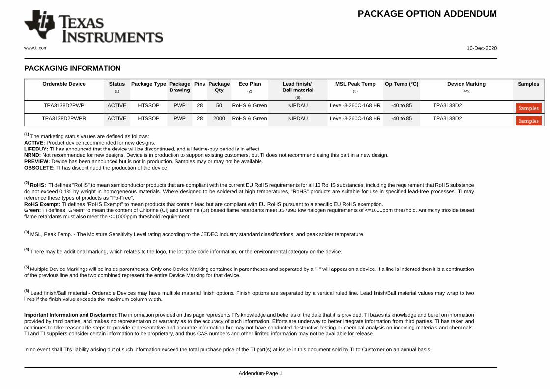
PACKAGING INFORMATION
Orderable Device Status(1)
Package Type PackageDrawing
Pins PackageQty
Eco Plan(2)
Lead finish/Ball material
(6)
MSL Peak Temp(3)
Op Temp (°C) Device Marking(4/5)
Samples
TPA3138D2PWP ACTIVE HTSSOP PWP 28 50 RoHS & Green NIPDAU Level-3-260C-168 HR -40 to 85 TPA3138D2
TPA3138D2PWPR ACTIVE HTSSOP PWP 28 2000 RoHS & Green NIPDAU Level-3-260C-168 HR -40 to 85 TPA3138D2
(1) The marketing status values are defined as follows:ACTIVE: Product device recommended for new designs.LIFEBUY: TI has announced that the device will be discontinued, and a lifetime-buy period is in effect.NRND: Not recommended for new designs. Device is in production to support existing customers, but TI does not recommend using this part in a new design.PREVIEW: Device has been announced but is not in production. Samples may or may not be available.OBSOLETE: TI has discontinued the production of the device.
(2) RoHS: TI defines "RoHS" to mean semiconductor products that are compliant with the current EU RoHS requirements for all 10 RoHS substances, including the requirement that RoHS substancedo not exceed 0.1% by weight in homogeneous materials. Where designed to be soldered at high temperatures, "RoHS" products are suitable for use in specified lead-free processes. TI mayreference these types of products as "Pb-Free".RoHS Exempt: TI defines "RoHS Exempt" to mean products that contain lead but are compliant with EU RoHS pursuant to a specific EU RoHS exemption.Green: TI defines "Green" to mean the content of Chlorine (Cl) and Bromine (Br) based flame retardants meet JS709B low halogen requirements of <=1000ppm threshold. Antimony trioxide basedflame retardants must also meet the <=1000ppm threshold requirement.
(3) MSL, Peak Temp. - The Moisture Sensitivity Level rating according to the JEDEC industry standard classifications, and peak solder temperature.
(4) There may be additional marking, which relates to the logo, the lot trace code information, or the environmental category on the device.
(5) Multiple Device Markings will be inside parentheses. Only one Device Marking contained in parentheses and separated by a "~" will appear on a device. If a line is indented then it is a continuationof the previous line and the two combined represent the entire Device Marking for that device.
(6) Lead finish/Ball material - Orderable Devices may have multiple material finish options. Finish options are separated by a vertical ruled line. Lead finish/Ball material values may wrap to twolines if the finish value exceeds the maximum column width.
Important Information and Disclaimer:The information provided on this page represents TI's knowledge and belief as of the date that it is provided. TI bases its knowledge and belief on informationprovided by third parties, and makes no representation or warranty as to the accuracy of such information. Efforts are underway to better integrate information from third parties. TI has taken andcontinues to take reasonable steps to provide representative and accurate information but may not have conducted destructive testing or chemical analysis on incoming materials and chemicals.TI and TI suppliers consider certain information to be proprietary, and thus CAS numbers and other limited information may not be available for release.
In no event shall TI's liability arising out of such information exceed the total purchase price of the TI part(s) at issue in this document sold by TI to Customer on an annual basis.

PACKAGE OPTION ADDENDUM
www.ti.com 10-Dec-2020
Addendum-Page 2

TAPE AND REEL INFORMATION
*All dimensions are nominal
Device PackageType
PackageDrawing
Pins SPQ ReelDiameter
(mm)
ReelWidth
W1 (mm)
A0(mm)
B0(mm)
K0(mm)
P1(mm)
W(mm)
Pin1Quadrant
TPA3138D2PWPR HTSSOP PWP 28 2000 330.0 16.4 6.9 10.2 1.8 12.0 16.0 Q1
PACKAGE MATERIALS INFORMATION
www.ti.com 5-Jan-2022
Pack Materials-Page 1

*All dimensions are nominal
Device Package Type Package Drawing Pins SPQ Length (mm) Width (mm) Height (mm)
TPA3138D2PWPR HTSSOP PWP 28 2000 350.0 350.0 43.0
PACKAGE MATERIALS INFORMATION
www.ti.com 5-Jan-2022
Pack Materials-Page 2

TUBE
*All dimensions are nominal
Device Package Name Package Type Pins SPQ L (mm) W (mm) T (µm) B (mm)
TPA3138D2PWP PWP HTSSOP 28 50 530 10.2 3600 3.5
PACKAGE MATERIALS INFORMATION
www.ti.com 5-Jan-2022
Pack Materials-Page 3

www.ti.com
GENERIC PACKAGE VIEW
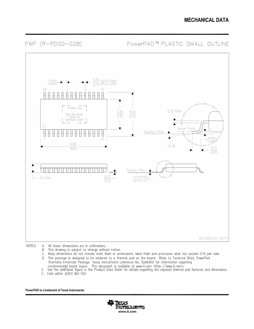
This image is a representation of the package family, actual package may vary.Refer to the product data sheet for package details.
TSSOP - 1.2 mm max heightTMPowerPADPWP 28SMALL OUTLINE PACKAGE4.4 x 9.7, 0.65 mm pitch
4224765/B

IMPORTANT NOTICE AND DISCLAIMERTI PROVIDES TECHNICAL AND RELIABILITY DATA (INCLUDING DATA SHEETS), DESIGN RESOURCES (INCLUDING REFERENCE DESIGNS), APPLICATION OR OTHER DESIGN ADVICE, WEB TOOLS, SAFETY INFORMATION, AND OTHER RESOURCES “AS IS” AND WITH ALL FAULTS, AND DISCLAIMS ALL WARRANTIES, EXPRESS AND IMPLIED, INCLUDING WITHOUT LIMITATION ANY IMPLIED WARRANTIES OF MERCHANTABILITY, FITNESS FOR A PARTICULAR PURPOSE OR NON-INFRINGEMENT OF THIRD PARTY INTELLECTUAL PROPERTY RIGHTS.These resources are intended for skilled developers designing with TI products. You are solely responsible for (1) selecting the appropriate TI products for your application, (2) designing, validating and testing your application, and (3) ensuring your application meets applicable standards, and any other safety, security, regulatory or other requirements.These resources are subject to change without notice. TI grants you permission to use these resources only for development of an application that uses the TI products described in the resource. Other reproduction and display of these resources is prohibited. No license is granted to any other TI intellectual property right or to any third party intellectual property right. TI disclaims responsibility for, and you will fully indemnify TI and its representatives against, any claims, damages, costs, losses, and liabilities arising out of your use of these resources.TI’s products are provided subject to TI’s Terms of Sale or other applicable terms available either on ti.com or provided in conjunction with such TI products. TI’s provision of these resources does not expand or otherwise alter TI’s applicable warranties or warranty disclaimers for TI products.TI objects to and rejects any additional or different terms you may have proposed. IMPORTANT NOTICE
Mailing Address: Texas Instruments, Post Office Box 655303, Dallas, Texas 75265Copyright © 2022, Texas Instruments Incorporated