Embed Size (px)
Citation preview

D-
D+
GND
VBUS
D-
D+
GND
VBUS
USB
Controller
D1-
D1+
D2-
D2+
GND
D-
D+
GND
VBUS
VCC
0.1µF
D3-
D3+
Product
Folder
Sample &Buy
Technical
Documents
Tools &
Software
Support &Community
ReferenceDesign
TPD6E001SLLS685D –JULY 2006–REVISED SEPTEMBER 2015
TPD6E001 Low-Capacitance 6-Channel ESD-Protection for High-Speed Data Interfaces1 Features 3 Description
The TPD6E001 is a six-channel Transient Voltage1• IEC 61000-4-2 Level 4 ESD Protection
Suppressor (TVS) based Electrostatic Discharge– ±8-kV IEC 61000-4-2 Contact Discharge (ESD) protection diode array. The TPD6E001 is rated– ±15-kV IEC 61000-4-2 Air-Gap Discharge to dissipate ESD strikes at the maximum level
specified in the IEC 61000-4-2 international standard• I/O Capacitance: 1.5-pF (Typical)(Level 4). This device has a 1.5-pF IO capacitance• Low Leakage Current: 1-nA (Maximum) per channel, making it ideal for use in high-speed
• Low Supply Current: 1-nA (Typical) data IO interfaces. The ultra low leakage current(<1 nA max) is suitable for precision analog• 0.9-V to 5.5-V Supply-Voltage Rangemeasurements in applications like glucose meters• Space-Saving RSE and RSF Package Optionsand heart rate monitors.
• Alternate 2-, 3-, 4-Channel Options Available:The TPD6E001 is available in space saving RSETPD2E2U06, TPD3E001, and TPD4E1U06(UQFN) and RSF (WQFN) packages and is specifiedfor –40°C to 85°C operation. Also see TPD2E2U06,2 ApplicationsTPD3E001, and TPD4E1U06 which are 2, 3, and 4
• End Equipments channel ESD protection options, respectively, forESD protection diode arrays with a different number– Portable Data Terminalof channels. The TPD2E2U06 provides a higher level– Industrial Monitor of IEC ESD protection, when compared to the
– IP Camera TPDxE001 family, and removes the need for an inputcapacitor. The TPD4E1U06 removes the need for an– Blood Glucose Metersinput capacitor, provides higher IEC ESD protection,• Interfacesand provides lower capacitance, when compared to
– SDIO the TPDxE001 family.– Precision Analog Interface
Device Information(1)– SVGA Connections
PART NUMBER PACKAGE BODY SIZE (NOM)– USB 2.0UQFN (10) 1.50 mm × 2.00 mm
TPD6E001WQFN (12) 4.00 mm × 4.00 mm
(1) For all available packages, see the orderable addendum atthe end of the datasheet.
Application Schematic
1
An IMPORTANT NOTICE at the end of this data sheet addresses availability, warranty, changes, use in safety-critical applications,intellectual property matters and other important disclaimers. PRODUCTION DATA.
TPD6E001SLLS685D –JULY 2006–REVISED SEPTEMBER 2015 www.ti.com
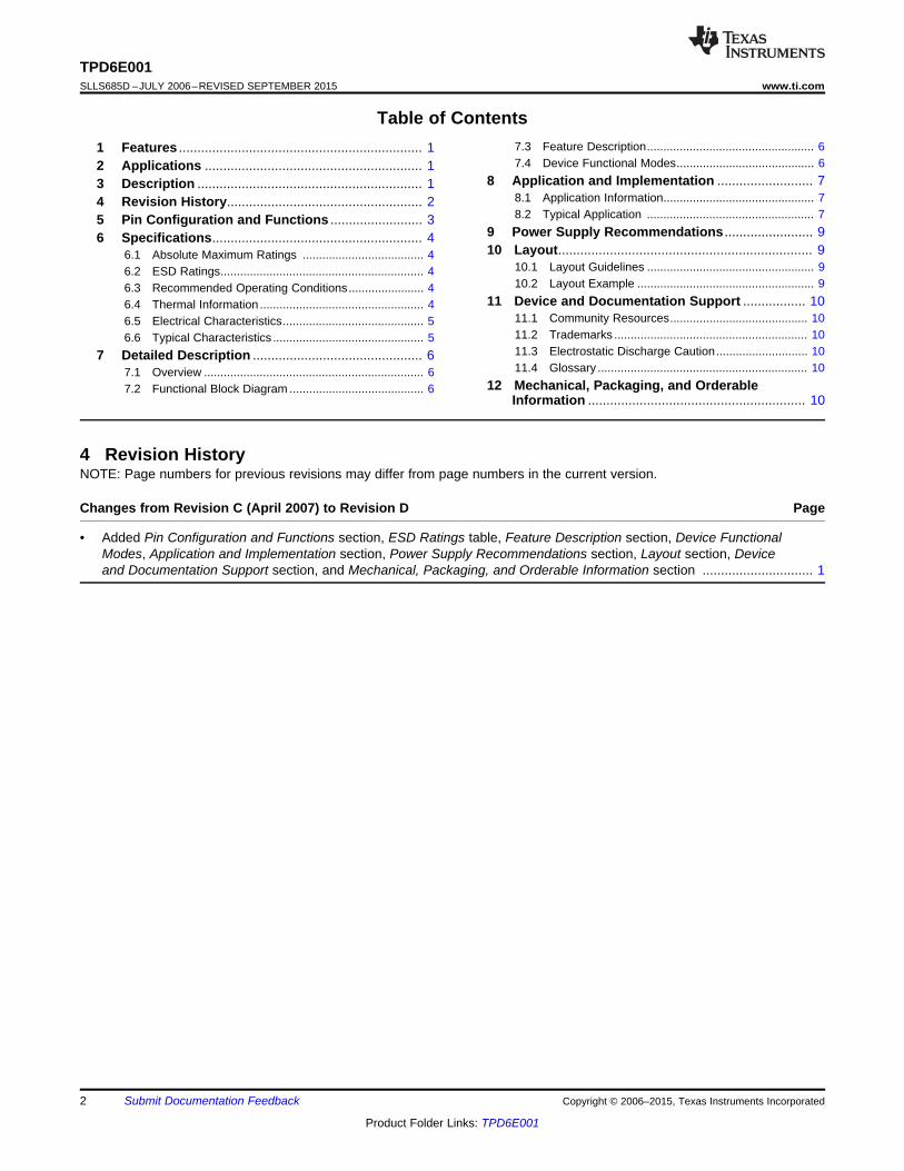
Table of Contents7.3 Feature Description................................................... 61 Features .................................................................. 17.4 Device Functional Modes.......................................... 62 Applications ........................................................... 1
8 Application and Implementation .......................... 73 Description ............................................................. 18.1 Application Information.............................................. 74 Revision History..................................................... 28.2 Typical Application ................................................... 75 Pin Configuration and Functions ......................... 3
9 Power Supply Recommendations ........................ 96 Specifications......................................................... 410 Layout..................................................................... 96.1 Absolute Maximum Ratings ..................................... 4
10.1 Layout Guidelines ................................................... 96.2 ESD Ratings.............................................................. 410.2 Layout Example ...................................................... 96.3 Recommended Operating Conditions....................... 4
11 Device and Documentation Support ................. 106.4 Thermal Information .................................................. 411.1 Community Resources.......................................... 106.5 Electrical Characteristics........................................... 511.2 Trademarks ........................................................... 106.6 Typical Characteristics .............................................. 511.3 Electrostatic Discharge Caution............................ 107 Detailed Description .............................................. 611.4 Glossary ................................................................ 107.1 Overview ................................................................... 6
12 Mechanical, Packaging, and Orderable7.2 Functional Block Diagram ......................................... 6Information ........................................................... 10
4 Revision HistoryNOTE: Page numbers for previous revisions may differ from page numbers in the current version.
Changes from Revision C (April 2007) to Revision D Page
• Added Pin Configuration and Functions section, ESD Ratings table, Feature Description section, Device FunctionalModes, Application and Implementation section, Power Supply Recommendations section, Layout section, Deviceand Documentation Support section, and Mechanical, Packaging, and Orderable Information section .............................. 1
2 Submit Documentation Feedback Copyright © 2006–2015, Texas Instruments Incorporated
Product Folder Links: TPD6E001

N.C
.
N.C
.
GND
VC
C
IO1
IO2
IO3
4 5 6
7
8
9
3
2
1
1112 10
IO1
N.C.
N.C.
GN
D
1
IO6
VC
C
IO5
IO2
IO3
IO4
2
5
6
7
8
9
10
3
4
TPD6E001www.ti.com SLLS685D –JULY 2006–REVISED SEPTEMBER 2015
5 Pin Configuration and Functions
RSE Package10-Pin UQFN
Top View
N.C.- Not internally connected
RSF Package12-Pin WQFN
Top View
N.C.- Not internally connected
Pin FunctionsPIN
TYPE DESCRIPTIONNAME RSE RSFGND 5 5 GND Ground
1, 2, 3, 1, 2, 3,IOx I/O ESD-protected channel6, 7, 8 7, 8, 9N.C. 4, 9 4, 6, 10, 12 — Not internally connectedVCC 10 11 Power Power-supply input. Bypass VCC to GND with a 0.1-μF ceramic capacitor.EP – EP GND Exposed pad. Connect to GND.
Copyright © 2006–2015, Texas Instruments Incorporated Submit Documentation Feedback 3
Product Folder Links: TPD6E001

TPD6E001SLLS685D –JULY 2006–REVISED SEPTEMBER 2015 www.ti.com
6 Specifications
6.1 Absolute Maximum Ratings (1)
over operating free-air temperature range (unless otherwise noted)MIN MAX UNIT
VCC –0.3 7 VVI/O –0.3 VCC + 0.3 VTJ Junction temperature 150 °C
Infrared (15 s) 220 °CBump temperature (soldering)
Vapor phase (60 s) 215 °CLead temperature (soldering, 10 s) 300 °C
Tstg Storage temperature –65 150 °C
(1) Stresses beyond those listed under Absolute Maximum Ratings may cause permanent damage to the device. These are stress ratingsonly, which do not imply functional operation of the device at these or any other conditions beyond those indicated under RecommendedOperating Conditions. Exposure to absolute-maximum-rated conditions for extended periods may affect device reliability.
6.2 ESD RatingsVALUE UNIT
Human body model (HBM), per ANSI/ESDA/JEDEC JS-001 (1) ±15000 VCharged-device model (CDM), per JEDEC specification JESD22- ±1000 VC101 (2)V(ESD) Electrostatic dischargeIEC 61000-4-2 Contact Discharge ±8000 VIEC 61000-4-2 Air-Gap Discharge ±15000 V
(1) JEDEC document JEP155 states that 500-V HBM allows safe manufacturing with a standard ESD control process.(2) JEDEC document JEP157 states that 250-V CDM allows safe manufacturing with a standard ESD control process.
6.3 Recommended Operating Conditionsover operating free-air temperature range (unless otherwise noted)
MIN NOM MAX UNITTA Operating free-air temperature range -40 85 °C
VCC Pin 0.9 5.5Operating Voltage V
IOx Pins 0 VCC
6.4 Thermal InformationTPD6E001
THERMAL METRIC (1) RSE (UQFN) RSF (WQFN) UNIT10 PINS 12 PINS
RθJA Junction-to-ambient thermal resistance 235.0 75.8 °C/WRθJC(top) Junction-to-case (top) thermal resistance 140.9 74.6 °C/WRθJB Junction-to-board thermal resistance 154.6 51.3 °C/WψJT Junction-to-top characterization parameter 21.8 5.9 °C/WψJB Junction-to-board characterization parameter 154.6 51.4 °C/WRθJC(bot) Junction-to-case (bottom) thermal resistance N/A 31.4 °C/W
(1) For more information about traditional and new thermal metrics, see the Semiconductor and IC Package Thermal Metrics applicationreport, SPRA953.
4 Submit Documentation Feedback Copyright © 2006–2015, Texas Instruments Incorporated
Product Folder Links: TPD6E001

0.00 1.00 2.00 2.50 3.00 4.00 5.00
IO Voltage (V)
1.00
1.20
1.40
1.60
1.80
2.00
2.20
IO C
ap
ac
ita
nc
e (
pF
)
1
10
100
1000
–40 25 45 65 85
Temperature (°C)
IO L
eakag
e C
urr
en
t (p
A)
TPD6E001www.ti.com SLLS685D –JULY 2006–REVISED SEPTEMBER 2015
6.5 Electrical CharacteristicsVCC = 5 V ± 10%, TA = -40°C to 85°C (unless otherwise noted)
PARAMETER TEST CONDITIONS MIN TYP (1) MAX UNITVCC Supply voltage 0.9 5.5 VICC Supply current 1 100 nAVF Diode forward voltage IF = 10 mA 0.65 0.95 VVBR Breakdown voltage IBR = 10 mA 11 V
Positive transients VCC + 25 VTA = 25°C, ±15-kV HBM,IF = 10 A Negative transients –25 VTA = 25°C, Positive transients VCC + 60 V±8-kV Contact DischargeVC Channel clamp voltage (2)
Negative transients –60 V(IEC 61000-4-2), IF = 24 ATA = 25°C, Positive transients VCC + 100 V±15-kV Air-Gap Discharge
Negative transients –100 V(IEC 61000-4-2), IF = 45 AIi/o Channel leakage current Vi/o = GND to VCC ±1 nACi/o Channel input capacitance VCC = 5 V, Bias of VCC/2 1.5 pF
(1) Typical values are at VCC = 5 V and TA = 25°C.(2) Channel clamp voltage is not production tested.
6.6 Typical Characteristics
Figure 2. IO Leakage Current vs TemperatureFigure 1. IO Capacitance vs IO Voltage(VCC = 5.5 V)(VCC = 5 V)
Copyright © 2006–2015, Texas Instruments Incorporated Submit Documentation Feedback 5
Product Folder Links: TPD6E001

IO5 IO6
GND
IO2 IO3 IO4IO1
VCC
TPD6E001SLLS685D –JULY 2006–REVISED SEPTEMBER 2015 www.ti.com
7 Detailed Description
7.1 OverviewThe TPD6E001 is a six-channel Transient Voltage Suppressor (TVS) based Electrostatic Discharge (ESD)protection diode array. The TPD6E001 is rated to dissipate ESD strikes at the maximum level specified in theIEC 61000-4-2 international standard (Level 4). This device has a 1.5-pF IO capacitance per channel, making itideal for use in high-speed data IO interfaces. The ultra low leakage current (< 1 nA maximum) is suitable forprecision analog measurements in applications like glucose meters and heart rate monitors.
7.2 Functional Block Diagram
7.3 Feature DescriptionTPD6E001 is a uni-directional ESD protection device with low capacitance. The device is constructed with acentral ESD clamp that features two hiding diodes per line to reduce the capacitive loading. This central ESDclamp is also connected to VCC to provide protection for the VCC line. Each IO line is rated to dissipate ESDstrikes at the maximum level specified in the IEC 61000-4-2 level 4 international standard. The TPD6E001's lowloading capacitance makes it ideal for protection high-speed signal terminals.
7.4 Device Functional ModesTPD6E001 is a passive-integrated circuit that activates whenever voltages above VBR or below the lower diodesVforward (–0.6V) are present upon the circuit being protected. During ESD events, voltages as high as ±15 kV canbe directed to ground and VCC via the internal diode network. Once the voltages on the protected lines fall belowthe trigger voltage of the TPD6E001 (usually within 10's of nano-seconds) the device reverts back to a high-impedance state.
6 Submit Documentation Feedback Copyright © 2006–2015, Texas Instruments Incorporated
Product Folder Links: TPD6E001

D-
D+
GND
VBUS
D-
D+
GND
VBUS
USB
Controller
D1-
D1+
D2-
D2+
GND
D-
D+
GND
VBUS
VCC
0.1µF
D3-
D3+
TPD6E001www.ti.com SLLS685D –JULY 2006–REVISED SEPTEMBER 2015
8 Application and Implementation
NOTEInformation in the following applications sections is not part of the TI componentspecification, and TI does not warrant its accuracy or completeness. TI’s customers areresponsible for determining suitability of components for their purposes. Customers shouldvalidate and test their design implementation to confirm system functionality.
8.1 Application InformationTPD6E001 is a diode array type Transient Voltage Suppressor (TVS) which is typically used to provide a path toground for dissipating ESD events on hi-speed signal lines between a human interface connector and a system.As the current from ESD passes through the TVS, only a small voltage drop is present across the diode. This isthe voltage presented to the protected IC. The low RDYN of the triggered TVS holds this voltage, VCLAMP, to atolerable level to the protected IC.
8.2 Typical Application
Figure 3. Typical Application Schematic
8.2.1 Design RequirementsFor this design example, a single TPD6E001 is used to protect all the pins of three USB2.0 connectors.
Given the USB application, the following parameters are known.
Table 1. Design ParametersDESIGN PARAMETER VALUE
Signal range on IO1, IO2, IO3, IO4, IO5, IO6 0 V to 3.6 VSignal voltage range on VCC 0 V to 5.25 V
Operating Frequency 240 MHz
Copyright © 2006–2015, Texas Instruments Incorporated Submit Documentation Feedback 7
Product Folder Links: TPD6E001

±40 ±30 ±20 ±10
0102030405060708090
100
±15 0 15 30 45 60 75 90 105 120 135 150
Vol
tage
(V
)
Time (nS) C001
TPD6E001SLLS685D –JULY 2006–REVISED SEPTEMBER 2015 www.ti.com
8.2.2 Detailed Design ProcedureWhen placed near the USB connectors, the TPD6E001 ESD solution offers little or no signal distortion duringnormal operation due to low IO capacitance and ultra-low leakage current specifications. The TPD6E001 ensuresthat the core circuitry is protected and the system is functioning properly in the event of an ESD strike. Forproper operation, the following layout/ design guidelines should be followed:1. Place the TPD6E001 solution close to the connectors. This allows the TPD6E001 to take away the energy
associated with ESD strike before it reaches the internal circuitry of the system board.2. Place a 0.1-μF capacitor very close to the VCC pin. This limits any momentary voltage surge at the IO pin
during the ESD strike event.3. Ensure that there is enough metallization for the VCC and GND loop. During normal operation, the TPD6E001
consumes 1 nA (max) leakage current. But during the ESD event, VCC and GND may see 15 A to30 A of current, depending on the ESD level. Sufficient current path enables safe discharge of all the energyassociated with the ESD strike.
4. Leave the unused IO pins floating. In this example of protecting three USB ports, none of the IO pins will beleft unused.
5. The VCC pin can be connected in two different ways:(a) If the VCC pin is connected to the system power supply, the TPD6E001 works as a transient suppressor
for any signal swing above VCC + VF. A 0.1-μF capacitor on the device VCC pin is recommended for ESDbypass.
(b) If the VCC pin is not connected to the system power supply, the TPD6E001 can tolerate higher signalswing in the range up to 10 V. Please note that a 0.1-μF capacitor is still recommended at the VCC pin forESD bypass.
8.2.3 Application CurveFigure 4 is a capture of the voltage clamping waveform of TPD6E001 on IO1 during a +8kV Contact IEC61000-4-2 ESD strike.
Figure 4. TPD6E001 +8kV Contact IEC61000-4-2 Voltage Clamping Waveform
8 Submit Documentation Feedback Copyright © 2006–2015, Texas Instruments Incorporated
Product Folder Links: TPD6E001

GND
GND
VCCIO1
IO2
IO4
IO5
IO6
N.C.
D1+
D1-
D2+
D2-
D3+
D3-
D1+
D1-
D2+
D2-
D3+
D3-
IO3
N.C.
0.1µF
= VIA to GND
= VIA to Bottom Layer
Bottom Layer
Top Layer
TPD6E001www.ti.com SLLS685D –JULY 2006–REVISED SEPTEMBER 2015
9 Power Supply RecommendationsTPD6E001 is a passive TVS diode, so there is no requirement to power this device. However, for best IEC61000-4-2 ESD performance and lowest capacitance performance, it is recommended that the VCC pin is biasedwith a 5V supply and that a 0.1µF capacitor is placed near the VCC pin. Take care to make sure that themaximum voltage specification for the VCC pin is not violated.
10 Layout
10.1 Layout Guidelines• The optimum placement is as close to the connector as possible.
– EMI during an ESD event can couple from the trace being struck to other nearby unprotected traces,resulting in early system failures.
– The PCB designer needs to minimize the possibility of EMI coupling by keeping any unprotected tracesaway from the protected traces which are between the TVS and the connector.
• Route the protected traces as straight as possible.• Eliminate any sharp corners on the protected traces between the TVS and the connector by using rounded
corners with the largest radii possible.– Electric fields tend to build up on corners, increasing EMI coupling.
10.2 Layout ExampleFigure 5 is an example of how to layout three differential data pairs with the TPD6E001. One example could beprotecting three USB2.0 ports from IEC ESD, as discussed in the Application and Implementation section.
Figure 5. Routing with the RSE Package
Copyright © 2006–2015, Texas Instruments Incorporated Submit Documentation Feedback 9
Product Folder Links: TPD6E001

TPD6E001SLLS685D –JULY 2006–REVISED SEPTEMBER 2015 www.ti.com
11 Device and Documentation Support
11.1 Community ResourcesThe following links connect to TI community resources. Linked contents are provided "AS IS" by the respectivecontributors. They do not constitute TI specifications and do not necessarily reflect TI's views; see TI's Terms ofUse.
TI E2E™ Online Community TI's Engineer-to-Engineer (E2E) Community. Created to foster collaborationamong engineers. At e2e.ti.com, you can ask questions, share knowledge, explore ideas and helpsolve problems with fellow engineers.
Design Support TI's Design Support Quickly find helpful E2E forums along with design support tools andcontact information for technical support.
11.2 TrademarksE2E is a trademark of Texas Instruments.All other trademarks are the property of their respective owners.
11.3 Electrostatic Discharge CautionThese devices have limited built-in ESD protection. The leads should be shorted together or the device placed in conductive foamduring storage or handling to prevent electrostatic damage to the MOS gates.
11.4 GlossarySLYZ022 — TI Glossary.
This glossary lists and explains terms, acronyms, and definitions.
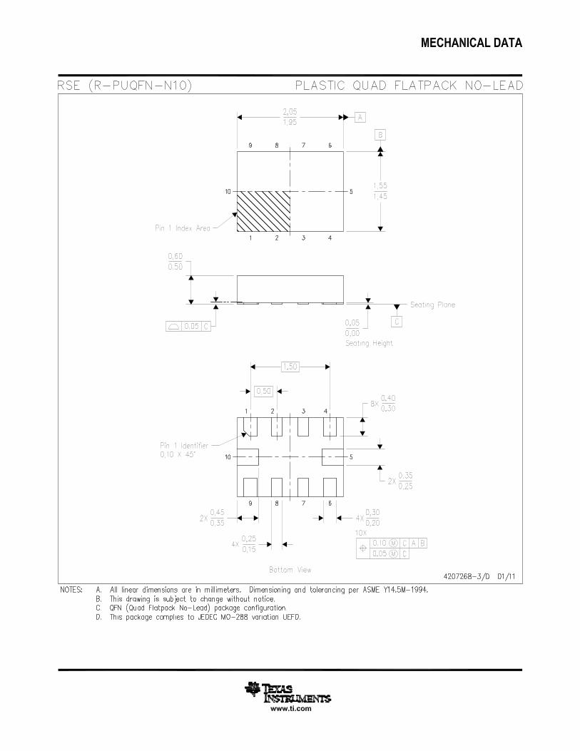
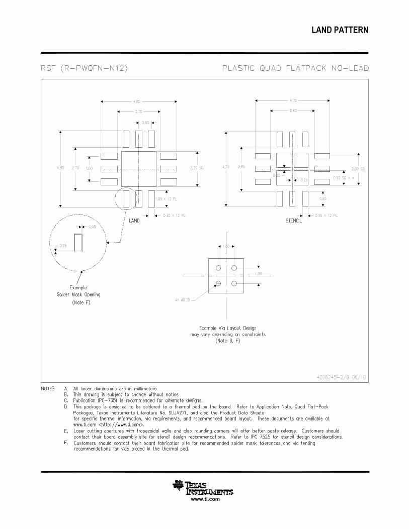
12 Mechanical, Packaging, and Orderable InformationThe following pages include mechanical, packaging, and orderable information. This information is the mostcurrent data available for the designated devices. This data is subject to change without notice and revision ofthis document. For browser-based versions of this data sheet, refer to the left-hand navigation.
10 Submit Documentation Feedback Copyright © 2006–2015, Texas Instruments Incorporated
Product Folder Links: TPD6E001

PACKAGE OPTION ADDENDUM
www.ti.com 24-Aug-2018
Addendum-Page 1
PACKAGING INFORMATION
Orderable Device Status(1)
Package Type PackageDrawing
Pins PackageQty
Eco Plan(2)
Lead/Ball Finish(6)
MSL Peak Temp(3)
Op Temp (°C) Device Marking(4/5)
Samples
TPD6E001RSER ACTIVE UQFN RSE 10 3000 Green (RoHS& no Sb/Br)
CU NIPDAU Level-1-260C-UNLIM -40 to 85 2DO
TPD6E001RSERG4 ACTIVE UQFN RSE 10 3000 Green (RoHS& no Sb/Br)
CU NIPDAU Level-1-260C-UNLIM -40 to 85 2DO
TPD6E001RSFR ACTIVE WQFN RSF 12 2000 Green (RoHS& no Sb/Br)
CU NIPDAU Level-1-260C-UNLIM -40 to 85 ZWN
(1) The marketing status values are defined as follows:ACTIVE: Product device recommended for new designs.LIFEBUY: TI has announced that the device will be discontinued, and a lifetime-buy period is in effect.NRND: Not recommended for new designs. Device is in production to support existing customers, but TI does not recommend using this part in a new design.PREVIEW: Device has been announced but is not in production. Samples may or may not be available.OBSOLETE: TI has discontinued the production of the device.
(2) RoHS: TI defines "RoHS" to mean semiconductor products that are compliant with the current EU RoHS requirements for all 10 RoHS substances, including the requirement that RoHS substancedo not exceed 0.1% by weight in homogeneous materials. Where designed to be soldered at high temperatures, "RoHS" products are suitable for use in specified lead-free processes. TI mayreference these types of products as "Pb-Free".RoHS Exempt: TI defines "RoHS Exempt" to mean products that contain lead but are compliant with EU RoHS pursuant to a specific EU RoHS exemption.Green: TI defines "Green" to mean the content of Chlorine (Cl) and Bromine (Br) based flame retardants meet JS709B low halogen requirements of <=1000ppm threshold. Antimony trioxide basedflame retardants must also meet the <=1000ppm threshold requirement.
(3) MSL, Peak Temp. - The Moisture Sensitivity Level rating according to the JEDEC industry standard classifications, and peak solder temperature.
(4) There may be additional marking, which relates to the logo, the lot trace code information, or the environmental category on the device.
(5) Multiple Device Markings will be inside parentheses. Only one Device Marking contained in parentheses and separated by a "~" will appear on a device. If a line is indented then it is a continuationof the previous line and the two combined represent the entire Device Marking for that device.
(6) Lead/Ball Finish - Orderable Devices may have multiple material finish options. Finish options are separated by a vertical ruled line. Lead/Ball Finish values may wrap to two lines if the finishvalue exceeds the maximum column width.
Important Information and Disclaimer:The information provided on this page represents TI's knowledge and belief as of the date that it is provided. TI bases its knowledge and belief on informationprovided by third parties, and makes no representation or warranty as to the accuracy of such information. Efforts are underway to better integrate information from third parties. TI has taken andcontinues to take reasonable steps to provide representative and accurate information but may not have conducted destructive testing or chemical analysis on incoming materials and chemicals.TI and TI suppliers consider certain information to be proprietary, and thus CAS numbers and other limited information may not be available for release.

PACKAGE OPTION ADDENDUM
www.ti.com 24-Aug-2018
Addendum-Page 2
In no event shall TI's liability arising out of such information exceed the total purchase price of the TI part(s) at issue in this document sold by TI to Customer on an annual basis.

TAPE AND REEL INFORMATION
*All dimensions are nominal
Device PackageType
PackageDrawing
Pins SPQ ReelDiameter
(mm)
ReelWidth
W1 (mm)
A0(mm)
B0(mm)
K0(mm)
P1(mm)
W(mm)
Pin1Quadrant
TPD6E001RSER UQFN RSE 10 3000 179.0 8.4 1.75 2.25 0.65 4.0 8.0 Q1
TPD6E001RSFR WQFN RSF 12 2000 330.0 12.4 4.3 4.3 1.1 8.0 12.0 Q2
PACKAGE MATERIALS INFORMATION
www.ti.com 3-Aug-2017
Pack Materials-Page 1

*All dimensions are nominal
Device Package Type Package Drawing Pins SPQ Length (mm) Width (mm) Height (mm)
TPD6E001RSER UQFN RSE 10 3000 203.0 203.0 35.0
TPD6E001RSFR WQFN RSF 12 2000 346.0 346.0 35.0
PACKAGE MATERIALS INFORMATION
www.ti.com 3-Aug-2017
Pack Materials-Page 2


IMPORTANT NOTICE
Texas Instruments Incorporated (TI) reserves the right to make corrections, enhancements, improvements and other changes to itssemiconductor products and services per JESD46, latest issue, and to discontinue any product or service per JESD48, latest issue. Buyersshould obtain the latest relevant information before placing orders and should verify that such information is current and complete.TI’s published terms of sale for semiconductor products (http://www.ti.com/sc/docs/stdterms.htm) apply to the sale of packaged integratedcircuit products that TI has qualified and released to market. Additional terms may apply to the use or sale of other types of TI products andservices.Reproduction of significant portions of TI information in TI data sheets is permissible only if reproduction is without alteration and isaccompanied by all associated warranties, conditions, limitations, and notices. TI is not responsible or liable for such reproduceddocumentation. Information of third parties may be subject to additional restrictions. Resale of TI products or services with statementsdifferent from or beyond the parameters stated by TI for that product or service voids all express and any implied warranties for theassociated TI product or service and is an unfair and deceptive business practice. TI is not responsible or liable for any such statements.Buyers and others who are developing systems that incorporate TI products (collectively, “Designers”) understand and agree that Designersremain responsible for using their independent analysis, evaluation and judgment in designing their applications and that Designers havefull and exclusive responsibility to assure the safety of Designers' applications and compliance of their applications (and of all TI productsused in or for Designers’ applications) with all applicable regulations, laws and other applicable requirements. Designer represents that, withrespect to their applications, Designer has all the necessary expertise to create and implement safeguards that (1) anticipate dangerousconsequences of failures, (2) monitor failures and their consequences, and (3) lessen the likelihood of failures that might cause harm andtake appropriate actions. Designer agrees that prior to using or distributing any applications that include TI products, Designer willthoroughly test such applications and the functionality of such TI products as used in such applications.TI’s provision of technical, application or other design advice, quality characterization, reliability data or other services or information,including, but not limited to, reference designs and materials relating to evaluation modules, (collectively, “TI Resources”) are intended toassist designers who are developing applications that incorporate TI products; by downloading, accessing or using TI Resources in anyway, Designer (individually or, if Designer is acting on behalf of a company, Designer’s company) agrees to use any particular TI Resourcesolely for this purpose and subject to the terms of this Notice.TI’s provision of TI Resources does not expand or otherwise alter TI’s applicable published warranties or warranty disclaimers for TIproducts, and no additional obligations or liabilities arise from TI providing such TI Resources. TI reserves the right to make corrections,enhancements, improvements and other changes to its TI Resources. TI has not conducted any testing other than that specificallydescribed in the published documentation for a particular TI Resource.Designer is authorized to use, copy and modify any individual TI Resource only in connection with the development of applications thatinclude the TI product(s) identified in such TI Resource. NO OTHER LICENSE, EXPRESS OR IMPLIED, BY ESTOPPEL OR OTHERWISETO ANY OTHER TI INTELLECTUAL PROPERTY RIGHT, AND NO LICENSE TO ANY TECHNOLOGY OR INTELLECTUAL PROPERTYRIGHT OF TI OR ANY THIRD PARTY IS GRANTED HEREIN, including but not limited to any patent right, copyright, mask work right, orother intellectual property right relating to any combination, machine, or process in which TI products or services are used. Informationregarding or referencing third-party products or services does not constitute a license to use such products or services, or a warranty orendorsement thereof. Use of TI Resources may require a license from a third party under the patents or other intellectual property of thethird party, or a license from TI under the patents or other intellectual property of TI.TI RESOURCES ARE PROVIDED “AS IS” AND WITH ALL FAULTS. TI DISCLAIMS ALL OTHER WARRANTIES ORREPRESENTATIONS, EXPRESS OR IMPLIED, REGARDING RESOURCES OR USE THEREOF, INCLUDING BUT NOT LIMITED TOACCURACY OR COMPLETENESS, TITLE, ANY EPIDEMIC FAILURE WARRANTY AND ANY IMPLIED WARRANTIES OFMERCHANTABILITY, FITNESS FOR A PARTICULAR PURPOSE, AND NON-INFRINGEMENT OF ANY THIRD PARTY INTELLECTUALPROPERTY RIGHTS. TI SHALL NOT BE LIABLE FOR AND SHALL NOT DEFEND OR INDEMNIFY DESIGNER AGAINST ANY CLAIM,INCLUDING BUT NOT LIMITED TO ANY INFRINGEMENT CLAIM THAT RELATES TO OR IS BASED ON ANY COMBINATION OFPRODUCTS EVEN IF DESCRIBED IN TI RESOURCES OR OTHERWISE. IN NO EVENT SHALL TI BE LIABLE FOR ANY ACTUAL,DIRECT, SPECIAL, COLLATERAL, INDIRECT, PUNITIVE, INCIDENTAL, CONSEQUENTIAL OR EXEMPLARY DAMAGES INCONNECTION WITH OR ARISING OUT OF TI RESOURCES OR USE THEREOF, AND REGARDLESS OF WHETHER TI HAS BEENADVISED OF THE POSSIBILITY OF SUCH DAMAGES.Unless TI has explicitly designated an individual product as meeting the requirements of a particular industry standard (e.g., ISO/TS 16949and ISO 26262), TI is not responsible for any failure to meet such industry standard requirements.Where TI specifically promotes products as facilitating functional safety or as compliant with industry functional safety standards, suchproducts are intended to help enable customers to design and create their own applications that meet applicable functional safety standardsand requirements. Using products in an application does not by itself establish any safety features in the application. Designers mustensure compliance with safety-related requirements and standards applicable to their applications. Designer may not use any TI products inlife-critical medical equipment unless authorized officers of the parties have executed a special contract specifically governing such use.Life-critical medical equipment is medical equipment where failure of such equipment would cause serious bodily injury or death (e.g., lifesupport, pacemakers, defibrillators, heart pumps, neurostimulators, and implantables). Such equipment includes, without limitation, allmedical devices identified by the U.S. Food and Drug Administration as Class III devices and equivalent classifications outside the U.S.TI may expressly designate certain products as completing a particular qualification (e.g., Q100, Military Grade, or Enhanced Product).Designers agree that it has the necessary expertise to select the product with the appropriate qualification designation for their applicationsand that proper product selection is at Designers’ own risk. Designers are solely responsible for compliance with all legal and regulatoryrequirements in connection with such selection.Designer will fully indemnify TI and its representatives against any damages, costs, losses, and/or liabilities arising out of Designer’s non-compliance with the terms and provisions of this Notice.
Mailing Address: Texas Instruments, Post Office Box 655303, Dallas, Texas 75265Copyright © 2018, Texas Instruments Incorporated