Embed Size (px)
Citation preview
SPI INTERFACEVOLATILE
REGISTERS
NON-VOLATILE
REGISTERS
HA
LA
HB
LB
WA
WB
VDD
GND
SCLK
DIN
CS
Product
Folder
Order
Now
Technical
Documents
Tools &
Software
Support &Community
An IMPORTANT NOTICE at the end of this data sheet addresses availability, warranty, changes, use in safety-critical applications,intellectual property matters and other important disclaimers. PRODUCTION DATA.
TPL0202SLIS135E –DECEMBER 2010–REVISED FEBRUARY 2017
TPL0202 256-Taps Dual Channel Digital Potentiometer With SPI and Non-Volatile Memory
1
1 Features1• Two Potentiometers With 256-Position Resolution• Non-Volatile Memory Stores Wiper Settings• 10-kΩ End-to-End Resistance (TPL0202-10)• Fast Power-Up Response Time: <100 µs• ±1 LSB INL, ±0.5 LSB DNL (Voltage-Divider
Mode)• 12 ppm/°C Ratiometric Temperature Coefficient• SPI Serial Interface• 2.7 to 5.5 V Single-Supply Operation• Operating Temperature Range From
–40°C to +105°C
2 Applications• Adjustable Gain Amplifiers and Offset Trimming• Adjustable Power Supplies• Precision Calibration of Set Point Thresholds• Sensor Trimming and Calibration• Mechanical Potentiometer Replacement
3 DescriptionThe TPL0202 has two linear-taper digitalpotentiometers (DPOTs) with 256 wiper positions.Each potentiometer can be used as a three-terminalpotentiometer or as a two-terminal rheostat. TheTPL0202-10 has an end-to-end resistance of 10 kΩ.
This DPOT can be used as a mechanicalpotentiometer replacement, allowing the user (orsoftware) to digitally control and adjust resistance.
The TPL0202 has non-volatile memory (EEPROM)which can be used to store the wiper position forautomatic recall upon power-up. The internalregisters of the TPL0202 can be accessed using aSPI-compatible digital interface.
Device Information(1)
PART NUMBER PACKAGE BODY SIZE (NOM)TPL0202 WQFN (16) 3.00 mm × 3.00 mm
(1) For all available packages, see the orderable addendum atthe end of the data sheet.
Simplified Schematic
2
TPL0202SLIS135E –DECEMBER 2010–REVISED FEBRUARY 2017 www.ti.com
Product Folder Links: TPL0202
Submit Documentation Feedback Copyright © 2010–2017, Texas Instruments Incorporated
Table of Contents1 Features .................................................................. 12 Applications ........................................................... 13 Description ............................................................. 14 Revision History..................................................... 25 Pin Configuration and Functions ......................... 36 Specifications......................................................... 4
6.1 Absolute Maximum Ratings ...................................... 46.2 ESD Ratings.............................................................. 46.3 Recommended Operating Conditions....................... 46.4 Thermal Information .................................................. 46.5 Electrical Characteristics........................................... 56.6 Operating Characteristics.......................................... 66.7 SPI Timing Requirements ......................................... 76.8 Typical Characteristics .............................................. 8
7 Detailed Description ............................................ 127.1 Overview ................................................................. 127.2 Functional Block Diagram ....................................... 127.3 Feature Description................................................. 137.4 Device Functional Modes........................................ 13
7.5 Programming........................................................... 217.6 Register Map........................................................... 22
8 Application and Implementation ........................ 248.1 Application Information............................................ 248.2 Typical Application .................................................. 24
9 Power Supply Recommendations ...................... 259.1 Power Sequence..................................................... 259.2 Wiper Position Upon Power Up .............................. 25
10 Layout................................................................... 2610.1 Layout Guidelines ................................................. 2610.2 Layout Example .................................................... 26
11 Device and Documentation Support ................. 2711.1 Documentation Support ........................................ 2711.2 Receiving Notification of Documentation Updates 2711.3 Community Resources.......................................... 2711.4 Trademarks ........................................................... 2711.5 Electrostatic Discharge Caution............................ 2711.6 Glossary ................................................................ 27
12 Mechanical, Packaging, and OrderableInformation ........................................................... 27
4 Revision HistoryNOTE: Page numbers for previous revisions may differ from page numbers in the current version.
Changes from Revision D (October 2015) to Revision E Page
• Changed "read endurance" to: "write endurance" .................................................................................................................. 6• Added Receiving Notification of Documentation Updates section ....................................................................................... 27
Changes from Revision C (June 2012) to Revision D Page
• Added Pin Functions table, ESD Ratings table, Thermal Information table, Detailed Description section, Applicationand Implementation section, Power Supply Recommendations section, Layout section, Device and DocumentationSupport section, and Mechanical, Packaging, and Orderable Information section................................................................ 1
• Fixed SPI Timing Requirements to show 5 MHz max SCLK frequency ............................................................................... 7
Changes from Revision B (August 2011) to Revision C Page
• Updated Pin Description Table............................................................................................................................................... 3
1 2 3 4
5
6
7
8
9101112
13
14
15
16
CS
N.C.
GND
N.C.
N.C.
N.C
.
LB
WB
HB
LA
WA
HA
N.C.
VD
D
SC
LK
DIN
EP
3
TPL0202www.ti.com SLIS135E –DECEMBER 2010–REVISED FEBRUARY 2017
Product Folder Links: TPL0202
Submit Documentation FeedbackCopyright © 2010–2017, Texas Instruments Incorporated
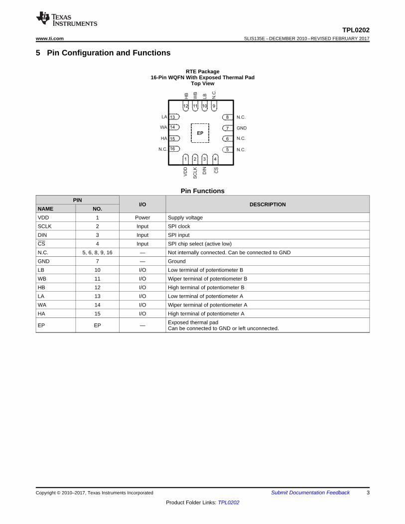
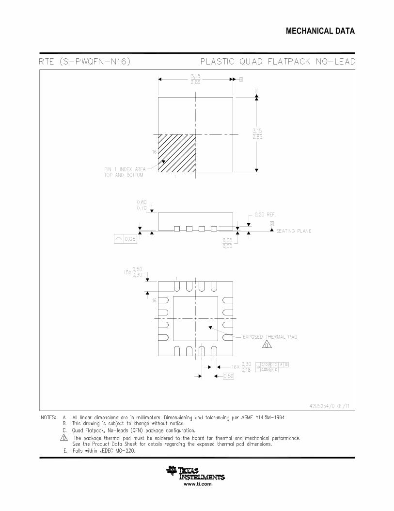
5 Pin Configuration and Functions
RTE Package16-Pin WQFN With Exposed Thermal Pad
Top View
Pin FunctionsPIN
I/O DESCRIPTIONNAME NO.VDD 1 Power Supply voltageSCLK 2 Input SPI clockDIN 3 Input SPI inputCS 4 Input SPI chip select (active low)N.C. 5, 6, 8, 9, 16 — Not internally connected. Can be connected to GNDGND 7 — GroundLB 10 I/O Low terminal of potentiometer BWB 11 I/O Wiper terminal of potentiometer BHB 12 I/O High terminal of potentiometer BLA 13 I/O Low terminal of potentiometer AWA 14 I/O Wiper terminal of potentiometer AHA 15 I/O High terminal of potentiometer A
EP EP — Exposed thermal padCan be connected to GND or left unconnected.
4
TPL0202SLIS135E –DECEMBER 2010–REVISED FEBRUARY 2017 www.ti.com
Product Folder Links: TPL0202
Submit Documentation Feedback Copyright © 2010–2017, Texas Instruments Incorporated
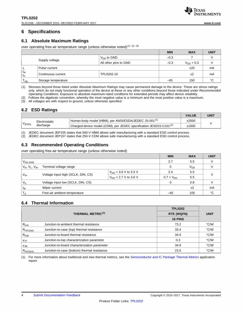
(1) Stresses beyond those listed under Absolute Maximum Ratings may cause permanent damage to the device. These are stress ratingsonly, which do not imply functional operation of the device at these or any other conditions beyond those indicated under RecommendedOperating Conditions. Exposure to absolute-maximum-rated conditions for extended periods may affect device reliability.
(2) Follows the algebraic convention, whereby the most negative value is a minimum and the most positive value is a maximum.(3) All voltages are with respect to ground, unless otherwise specified.
6 Specifications
6.1 Absolute Maximum Ratingsover operating free-air temperature range (unless otherwise noted) (1) (2) (3)
MIN MAX UNIT
Supply voltageVDD to GND –0.3 7 VAll other pins to GND –0.3 VDD + 0.3 V
ILIWIH
Pulse current ±20 mA
Continuous current TPL0202-10 ±2 mA
Tstg Storage temperature –65 150 °C
(1) JEDEC document JEP155 states that 500-V HBM allows safe manufacturing with a standard ESD control process.(2) JEDEC document JEP157 states that 250-V CDM allows safe manufacturing with a standard ESD control process.
6.2 ESD RatingsVALUE UNIT
V(ESD)Electrostaticdischarge
Human-body model (HBM), per ANSI/ESDA/JEDEC JS-001 (1) ±2500V
Charged-device model (CDM), per JEDEC specification JESD22-C101 (2) ±1000
6.3 Recommended Operating Conditionsover operating free-air temperature range (unless otherwise noted)
MIN MAX UNITVDD,GND 2.7 5.5 VVH, VL, VW Terminal voltage range 0 VDD V
VIH Voltage input high (SCLK, DIN, CS)VDD = 3.6 V to 5.5 V 2.4 5.5
VVDD = 2.7 V to 3.6 V 0.7 × VDD 5.5
VIL Voltage input low (SCLK, DIN, CS) 0 0.8 VIW Wiper current ±2 mATA Free-air ambient temperature –40 105 °C
(1) For more information about traditional and new thermal metrics, see the Semiconductor and IC Package Thermal Metrics applicationreport.
6.4 Thermal Information
THERMAL METRIC (1)TPL0202
UNITRTE (WQFN)16 PINS
RθJA Junction-to-ambient thermal resistance 73.2 °C/WRθJC(top) Junction-to-case (top) thermal resistance 33.4 °C/WRθJB Junction-to-board thermal resistance 34.9 °C/WψJT Junction-to-top characterization parameter 0.3 °C/WψJB Junction-to-board characterization parameter 34.9 °C/WRθJC(bot) Junction-to-case (bottom) thermal resistance 23.5 °C/W
H
L
WR
TOTAL
CL
CH
CW
k
i
ii V 0 for k i
i
IY
V= ¹
=
5
TPL0202www.ti.com SLIS135E –DECEMBER 2010–REVISED FEBRUARY 2017
Product Folder Links: TPL0202
Submit Documentation FeedbackCopyright © 2010–2017, Texas Instruments Incorporated
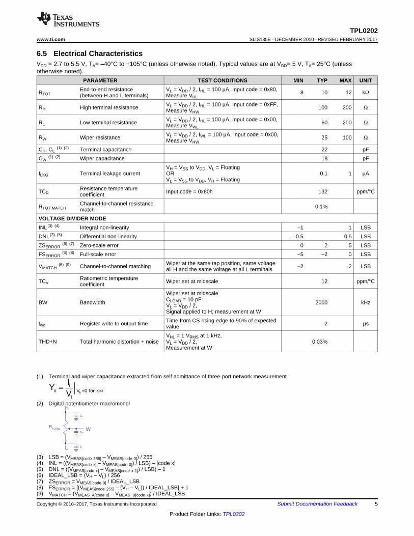
(1) Terminal and wiper capacitance extracted from self admittance of three-port network measurement
(2) Digital potentiometer macromodel
(3) LSB = (VMEAS[code 255] – VMEAS[code 0]) / 255(4) INL = ((VMEAS[code x] – VMEAS[code 0]) / LSB) – [code x](5) DNL = ((VMEAS[code x] – VMEAS[code x-1]) / LSB) – 1(6) IDEAL_LSB = (VH – VL) / 256(7) ZSERROR = VMEAS[code 0] / IDEAL_LSB(8) FSERROR = [(VMEAS[code 255] – (VH – VL)) / IDEAL_LSB] + 1(9) VMATCH = (VMEAS_A[code x] – VMEAS_B[code x]) / IDEAL_LSB
6.5 Electrical CharacteristicsVDD = 2.7 to 5.5 V, TA= –40°C to +105°C (unless otherwise noted). Typical values are at VDD= 5 V, TA= 25°C (unlessotherwise noted).
PARAMETER TEST CONDITIONS MIN TYP MAX UNIT
RTOTEnd-to-end resistance(between H and L terminals)
VL = VDD / 2, IHL = 100 µA, Input code = 0x80,Measure VHL
8 10 12 kΩ
RH High terminal resistance VL = VDD / 2, IHL = 100 µA, Input code = 0xFF,Measure VHW
100 200 Ω
RL Low terminal resistance VL = VDD / 2, IHL = 100 µA, Input code = 0x00,Measure VWL
60 200 Ω
RW Wiper resistance VL = VDD / 2, IWL = 100 µA, Input code = 0x00,Measure VHW
25 100 Ω
CH, CL(1) (2) Terminal capacitance 22 pF
CW(1) (2) Wiper capacitance 18 pF
ILKG Terminal leakage currentVH = VSS to VDD, VL = FloatingORVL = VSS to VDD, VH = Floating
0.1 1 µA
TCRResistance temperaturecoefficient Input code = 0x80h 132 ppm/°C
RTOT,MATCHChannel-to-channel resistancematch 0.1%
VOLTAGE DIVIDER MODEINL (3) (4) Integral non-linearity –1 1 LSBDNL (3) (5) Differential non-linearity –0.5 0.5 LSBZSERROR
(6) (7) Zero-scale error 0 2 5 LSBFSERROR
(6) (8) Full-scale error –5 –2 0 LSB
VMATCH(6) (9) Channel-to-channel matching Wiper at the same tap position, same voltage
all H and the same voltage at all L terminals –2 2 LSB
TCVRatiometric temperaturecoefficient Wiper set at midscale 12 ppm/°C
BW Bandwidth
Wiper set at midscaleCLOAD = 10 pFVL = VDD / 2,Signal applied to H; measurement at W
2000 kHz
two Register write to output time Time from CS rising edge to 90% of expectedvalue 2 µs
THD+N Total harmonic distortion + noiseVHL = 1 VRMS at 1 kHz,VL = VDD / 2,Measurement at W
0.03%
6
TPL0202SLIS135E –DECEMBER 2010–REVISED FEBRUARY 2017 www.ti.com
Product Folder Links: TPL0202
Submit Documentation Feedback Copyright © 2010–2017, Texas Instruments Incorporated
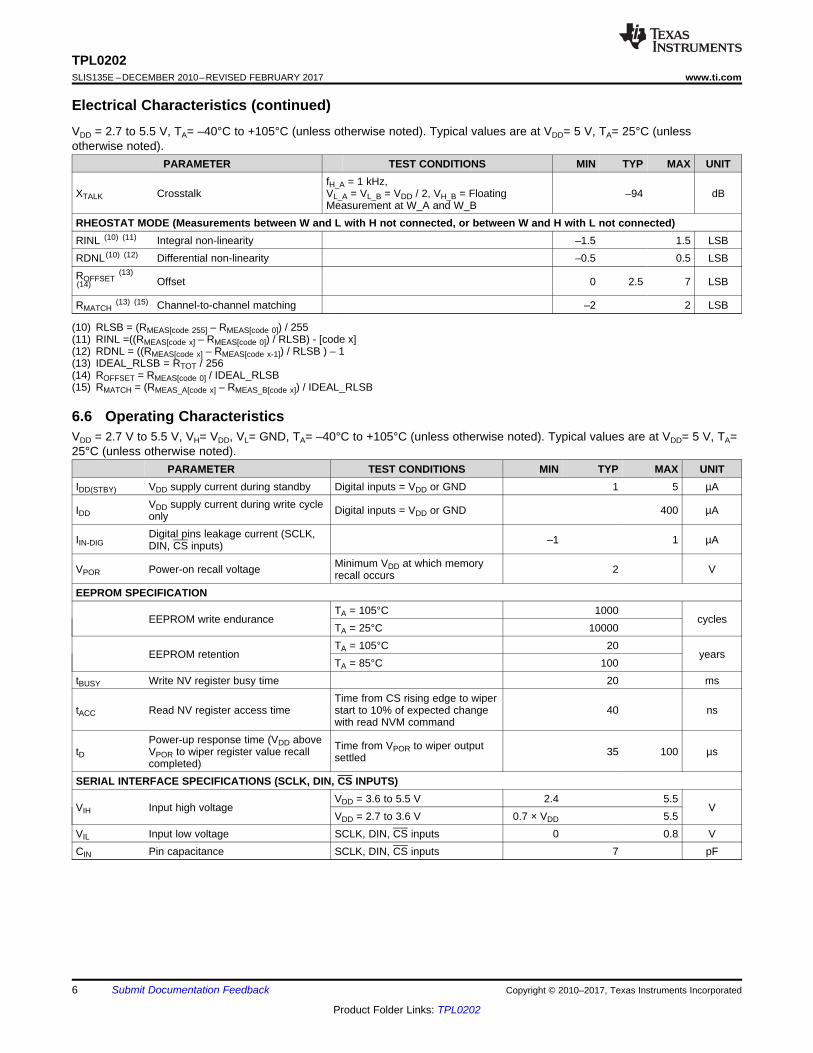
Electrical Characteristics (continued)VDD = 2.7 to 5.5 V, TA= –40°C to +105°C (unless otherwise noted). Typical values are at VDD= 5 V, TA= 25°C (unlessotherwise noted).
PARAMETER TEST CONDITIONS MIN TYP MAX UNIT
(10) RLSB = (RMEAS[code 255] – RMEAS[code 0]) / 255(11) RINL =((RMEAS[code x] – RMEAS[code 0]) / RLSB) - [code x](12) RDNL = ((RMEAS[code x] – RMEAS[code x-1]) / RLSB ) – 1(13) IDEAL_RLSB = RTOT / 256(14) ROFFSET = RMEAS[code 0] / IDEAL_RLSB(15) RMATCH = (RMEAS_A[code x] – RMEAS_B[code x]) / IDEAL_RLSB
XTALK CrosstalkfH_A = 1 kHz,VL_A = VL_B = VDD / 2, VH_B = FloatingMeasurement at W_A and W_B
–94 dB
RHEOSTAT MODE (Measurements between W and L with H not connected, or between W and H with L not connected)RINL (10) (11) Integral non-linearity –1.5 1.5 LSBRDNL (10) (12) Differential non-linearity –0.5 0.5 LSBROFFSET
(13)(14) Offset 0 2.5 7 LSB
RMATCH(13) (15) Channel-to-channel matching –2 2 LSB
6.6 Operating CharacteristicsVDD = 2.7 V to 5.5 V, VH= VDD, VL= GND, TA= –40°C to +105°C (unless otherwise noted). Typical values are at VDD= 5 V, TA=25°C (unless otherwise noted).
PARAMETER TEST CONDITIONS MIN TYP MAX UNITIDD(STBY) VDD supply current during standby Digital inputs = VDD or GND 1 5 µA
IDDVDD supply current during write cycleonly Digital inputs = VDD or GND 400 µA
IIN-DIGDigital pins leakage current (SCLK,DIN, CS inputs) –1 1 µA
VPOR Power-on recall voltage Minimum VDD at which memoryrecall occurs 2 V
EEPROM SPECIFICATION
EEPROM write enduranceTA = 105°C 1000
cyclesTA = 25°C 10000
EEPROM retentionTA = 105°C 20
yearsTA = 85°C 100
tBUSY Write NV register busy time 20 ms
tACC Read NV register access timeTime from CS rising edge to wiperstart to 10% of expected changewith read NVM command
40 ns
tDPower-up response time (VDD aboveVPOR to wiper register value recallcompleted)
Time from VPOR to wiper outputsettled 35 100 µs
SERIAL INTERFACE SPECIFICATIONS (SCLK, DIN, CS INPUTS)
VIH Input high voltageVDD = 3.6 to 5.5 V 2.4 5.5
VVDD = 2.7 to 3.6 V 0.7 × VDD 5.5
VIL Input low voltage SCLK, DIN, CS inputs 0 0.8 VCIN Pin capacitance SCLK, DIN, CS inputs 7 pF
7
TPL0202www.ti.com SLIS135E –DECEMBER 2010–REVISED FEBRUARY 2017
Product Folder Links: TPL0202
Submit Documentation FeedbackCopyright © 2010–2017, Texas Instruments Incorporated
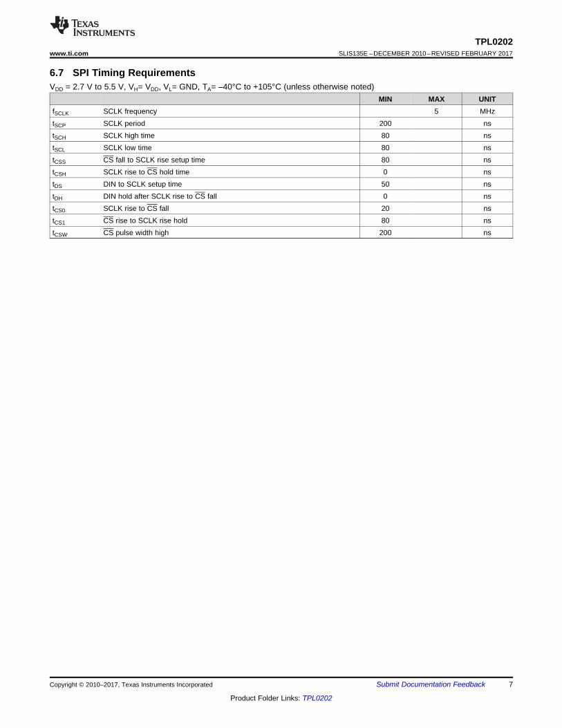
6.7 SPI Timing RequirementsVDD = 2.7 V to 5.5 V, VH= VDD, VL= GND, TA= –40°C to +105°C (unless otherwise noted)
MIN MAX UNITfSCLK SCLK frequency 5 MHztSCP SCLK period 200 nstSCH SCLK high time 80 nstSCL SCLK low time 80 nstCSS CS fall to SCLK rise setup time 80 nstCSH SCLK rise to CS hold time 0 nstDS DIN to SCLK setup time 50 nstDH DIN hold after SCLK rise to CS fall 0 nstCS0 SCLK rise to CS fall 20 nstCS1 CS rise to SCLK rise hold 80 nstCSW CS pulse width high 200 ns
Digital Code
DN
L (L
SB
)
0 32 64 96 128 160 192 224 256-0.2
-0.1
0
0.1
0.2
0.3
D007
2.7 V5 V5.5 V
Digital Code
INL
(LS
B)
0 32 64 96 128 160 192 224 256-0.1
0
0.1
0.2
0.3
D006
2.7 V5 V5.5 V
Digital Code
DN
L (L
SB
)
0 32 64 96 128 160 192 224 256-0.3
-0.2
-0.1
0
0.1
0.2
0.3
D004
VDD = 5 V -40 C 25 C105 C
Digital Code
INL
(LS
B)
0 32 64 96 128 160 192 224 256-0.1
0
0.1
0.2
0.3
D005
VDD = 5 V-40 C 25 C105 C
TA - Free-Air Temperature (C)
I DD
(S
TB
Y) -
Sta
ndby
Cur
rent
(µ
A)
-40 -15 10 35 60 85 1050
0.5
1
1.5
2
2.5
D002
2.7 V3.6 V5.5 V
0 0.5 1 1.5 2 2.5 3 3.5 4 4.5 5
V - Input Voltage - VI
0
1
10
100
1000
10000
I-
Su
pp
ly C
urr
en
t -
AD
Dm
V = 2.7 VDD
V = 5 VDD
8
TPL0202SLIS135E –DECEMBER 2010–REVISED FEBRUARY 2017 www.ti.com
Product Folder Links: TPL0202
Submit Documentation Feedback Copyright © 2010–2017, Texas Instruments Incorporated
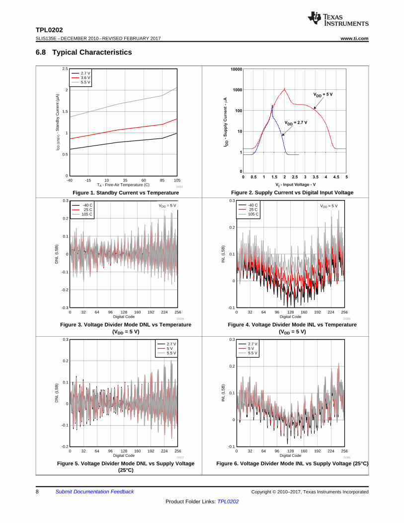
6.8 Typical Characteristics
Figure 1. Standby Current vs Temperature Figure 2. Supply Current vs Digital Input Voltage
Figure 3. Voltage Divider Mode DNL vs Temperature(VDD = 5 V)
Figure 4. Voltage Divider Mode INL vs Temperature(VDD = 5 V)
Figure 5. Voltage Divider Mode DNL vs Supply Voltage(25°C)
Figure 6. Voltage Divider Mode INL vs Supply Voltage (25°C)
Digital Code
RIN
L (L
SB
)
0 32 64 96 128 160 192 224 256-0.3
-0.2
-0.1
0
0.1
0.2
0.3
0.4
D0011
VDD = 5 V-40 C 25 C105 C
Digital Code
RD
NL
(LS
B)
0 32 64 96 128 160 192 224 256-0.3
-0.2
-0.1
0
0.1
0.2
0.3
D012
VDD = 5 V-40 C 25 C105 C
0
100
200
300
400
16 80 144 208Digital Code
5.5 V
5 V
2.7 V
TC
(p
pm
/C)
TA - Free-air Temperature (C)
FS
Err
or (
LSB
)
-40 -15 10 35 60 85 110-4
-3.5
-3
-2.5
-2
-1.5
-1
-0.5
0
D009
2.7 V5 V5.5 V
Digital Code
Una
djus
ted
Err
or (
LSB
)
0 32 64 96 128 160 192 224 256-2.5
-2
-1.5
-1
-0.5
0
0.5
1
1.5
2
2.5
D001
-40 C 25 C105 C
TA - Free-Air Temperature (C)
ZS
Err
or (
LSB
)
-40 -15 10 35 60 85 1100
0.5
1
1.5
2
2.5
3
D008
2.7 V5 V5.5 V
9
TPL0202www.ti.com SLIS135E –DECEMBER 2010–REVISED FEBRUARY 2017
Product Folder Links: TPL0202
Submit Documentation FeedbackCopyright © 2010–2017, Texas Instruments Incorporated
Typical Characteristics (continued)
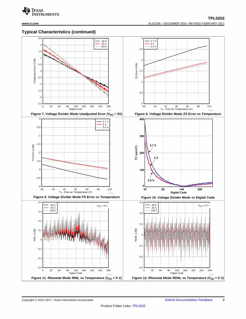
Figure 7. Voltage Divider Mode Unadjusted Error (VDD = 5V) Figure 8. Voltage Divider Mode ZS Error vs Temperature
Figure 9. Voltage Divider Mode FS Error vs Temperature Figure 10. Voltage Divider Mode vs Digital Code
Figure 11. Rheostat Mode RINL vs Temperature (VDD = 5 V) Figure 12. Rheostat Mode RDNL vs Temperature (VDD = 5 V)
VI - Input Voltage (V)
Ter
min
al R
esis
tanc
e (O
hms)
0 0.3 0.6 0.9 1.2 1.5 1.8 2.1 2.4 2.70
20
40
60
80
100
120
140
160
180
200
D017
RWRLRH
VI - Input Voltage (V)
Ter
min
al R
esis
tanc
e (O
hms)
0 0.5 1 1.5 2 2.5 3 3.5 4 4.5 50
20
40
60
80
100
120
140
160
180
200
D018
RWRLRH
0
100
200
300
400
500
600
16 80 144 208
Digital Code
5.5 V
5 V
2.7 V
TC
- (
pp
m/C
)
TA - Free-Air Temperature (C)
Offs
et E
rror
(LS
B)
-40 -15 10 35 60 85 1050
0.5
1
1.5
2
2.5
3
3.5
4
4.5
5
D016
2.7 V5 V5.5 V
Digital Code
RIN
L (L
SB
)
0 32 64 96 128 160 192 224 256-0.2
-0.1
0
0.1
0.2
0.3
0.4
D013
2.7 V5 V5.5 V
Digital Code
RD
NL
(LS
B)
0 32 64 96 128 160 192 224 256-0.2
-0.1
0
0.1
0.2
0.3
D014
2.7 V5 V5.5 V
10
TPL0202SLIS135E –DECEMBER 2010–REVISED FEBRUARY 2017 www.ti.com
Product Folder Links: TPL0202
Submit Documentation Feedback Copyright © 2010–2017, Texas Instruments Incorporated
Typical Characteristics (continued)
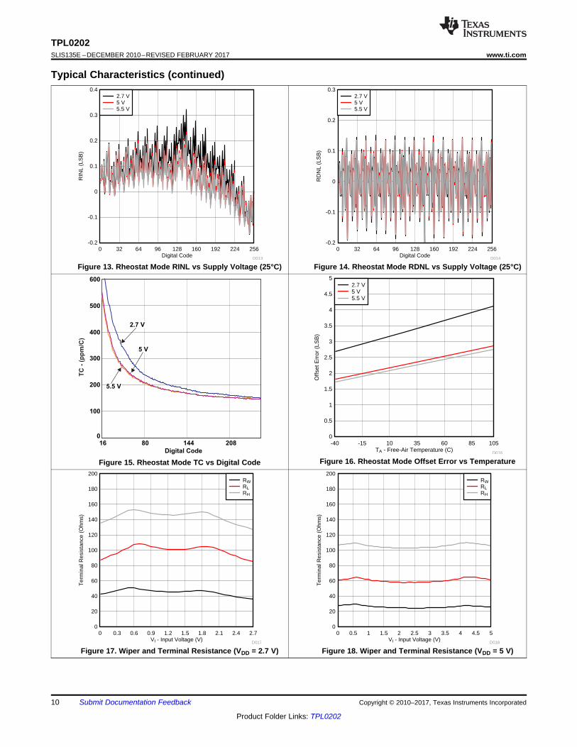
Figure 13. Rheostat Mode RINL vs Supply Voltage (25°C) Figure 14. Rheostat Mode RDNL vs Supply Voltage (25°C)
Figure 15. Rheostat Mode TC vs Digital Code Figure 16. Rheostat Mode Offset Error vs Temperature
Figure 17. Wiper and Terminal Resistance (VDD = 2.7 V) Figure 18. Wiper and Terminal Resistance (VDD = 5 V)
-0.5
0.5
1.0
1.5
2.0
2.5
3.0
3.5
4.0
4.5
5.0
5.5
0 10 20 30 40 50 60 70 80 90 100
t - Time - Sm
Vo
ltag
e -
V
VDD
Wiper
0.0
TA - Free-air Temperature (C)
Res
ista
nce
Cha
nge
(%)
-40 -15 10 35 60 85 105-1
-0.5
0
0.5
1
1.5
D019
2.7 V5 V5.5 V
2.47
2.48
2.46
2.50
2.51
2.52
2.53
2.54
2.55
2.56
2.57
0 0.5 1 1.5 2 2.5 3 3.5 4 4.5 5
t - Time - Sm
Vo
lta
ge
- V
11
TPL0202www.ti.com SLIS135E –DECEMBER 2010–REVISED FEBRUARY 2017
Product Folder Links: TPL0202
Submit Documentation FeedbackCopyright © 2010–2017, Texas Instruments Incorporated
Typical Characteristics (continued)
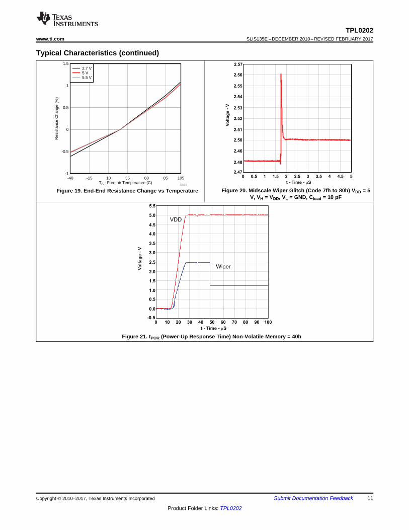
Figure 19. End-End Resistance Change vs Temperature Figure 20. Midscale Wiper Glitch (Code 7fh to 80h) VDD = 5V, VH = VDD, VL = GND, Cload = 10 pF
Figure 21. tPOR (Power-Up Response Time) Non-Volatile Memory = 40h
SPI INTERFACEVOLATILE
REGISTERS
NON-VOLATILE
REGISTERS
HA
LA
HB
LB
WA
WB
VDD
GND
SCLK
DIN
CS
12
TPL0202SLIS135E –DECEMBER 2010–REVISED FEBRUARY 2017 www.ti.com
Product Folder Links: TPL0202
Submit Documentation Feedback Copyright © 2010–2017, Texas Instruments Incorporated
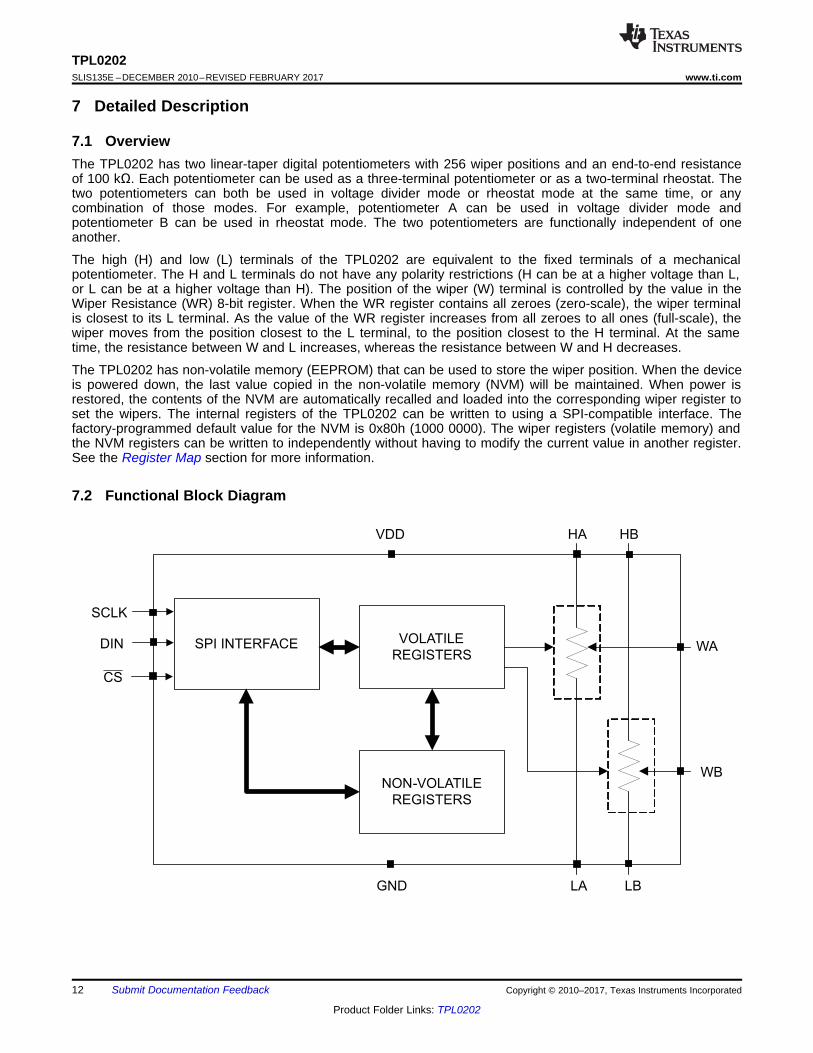
7 Detailed Description
7.1 OverviewThe TPL0202 has two linear-taper digital potentiometers with 256 wiper positions and an end-to-end resistanceof 100 kΩ. Each potentiometer can be used as a three-terminal potentiometer or as a two-terminal rheostat. Thetwo potentiometers can both be used in voltage divider mode or rheostat mode at the same time, or anycombination of those modes. For example, potentiometer A can be used in voltage divider mode andpotentiometer B can be used in rheostat mode. The two potentiometers are functionally independent of oneanother.
The high (H) and low (L) terminals of the TPL0202 are equivalent to the fixed terminals of a mechanicalpotentiometer. The H and L terminals do not have any polarity restrictions (H can be at a higher voltage than L,or L can be at a higher voltage than H). The position of the wiper (W) terminal is controlled by the value in theWiper Resistance (WR) 8-bit register. When the WR register contains all zeroes (zero-scale), the wiper terminalis closest to its L terminal. As the value of the WR register increases from all zeroes to all ones (full-scale), thewiper moves from the position closest to the L terminal, to the position closest to the H terminal. At the sametime, the resistance between W and L increases, whereas the resistance between W and H decreases.
The TPL0202 has non-volatile memory (EEPROM) that can be used to store the wiper position. When the deviceis powered down, the last value copied in the non-volatile memory (NVM) will be maintained. When power isrestored, the contents of the NVM are automatically recalled and loaded into the corresponding wiper register toset the wipers. The internal registers of the TPL0202 can be written to using a SPI-compatible interface. Thefactory-programmed default value for the NVM is 0x80h (1000 0000). The wiper registers (volatile memory) andthe NVM registers can be written to independently without having to modify the current value in another register.See the Register Map section for more information.
7.2 Functional Block Diagram
( )HW H L
DV V V 1
256
æ öæ ö= - ´ -ç ÷ç ÷è øè ø
( )W WL H L
DV V V V
256= = - ´
H
L
W
VHW
VH - VL
VWL
13
TPL0202www.ti.com SLIS135E –DECEMBER 2010–REVISED FEBRUARY 2017
Product Folder Links: TPL0202
Submit Documentation FeedbackCopyright © 2010–2017, Texas Instruments Incorporated
7.3 Feature Description
7.3.1 Dual Channel, 256-Position ResolutionThe TPL0202 features two independent DPOTs. Each DPOT is capable of being used and controlledindependently of the other one.
7.3.2 Non-Volatile MemoryThe TPL0202 device features non-volatile memory which is used to store the wiper positions of bothpotentiometers independently. This allows the user to set the default power-up position of the wiper. By default,this is 0x80h (midscale).
7.4 Device Functional Modes
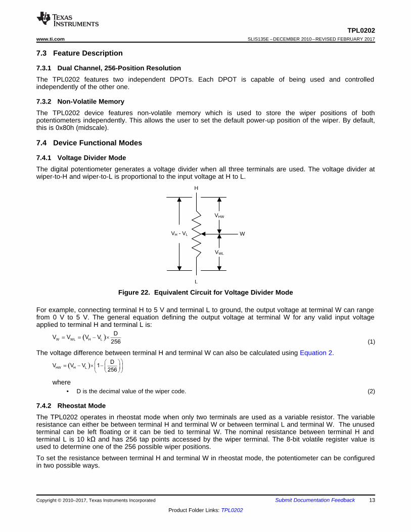
7.4.1 Voltage Divider ModeThe digital potentiometer generates a voltage divider when all three terminals are used. The voltage divider atwiper-to-H and wiper-to-L is proportional to the input voltage at H to L.
Figure 22. Equivalent Circuit for Voltage Divider Mode
For example, connecting terminal H to 5 V and terminal L to ground, the output voltage at terminal W can rangefrom 0 V to 5 V. The general equation defining the output voltage at terminal W for any valid input voltageapplied to terminal H and terminal L is:
(1)
The voltage difference between terminal H and terminal W can also be calculated using Equation 2.
where• D is the decimal value of the wiper code. (2)
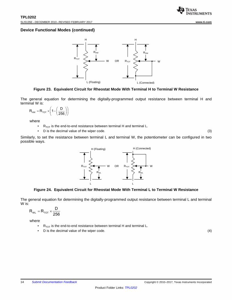
7.4.2 Rheostat ModeThe TPL0202 operates in rheostat mode when only two terminals are used as a variable resistor. The variableresistance can either be between terminal H and terminal W or between terminal L and terminal W. The unusedterminal can be left floating or it can be tied to terminal W. The nominal resistance between terminal H andterminal L is 10 kΩ and has 256 tap points accessed by the wiper terminal. The 8-bit volatile register value isused to determine one of the 256 possible wiper positions.
To set the resistance between terminal H and terminal W in rheostat mode, the potentiometer can be configuredin two possible ways.
WL TOT
DR R
256= ´
H (Floating)
L
W
H (Connected)
L
W
RWL RWL
RTOT RTOTOR
HW TOT
DR R 1
256
æ öæ ö= ´ -ç ÷ç ÷
è øè ø
H
L (Floating)
W
H
L (Connected)
W
RHW RHW
RTOTRTOTOR
14
TPL0202SLIS135E –DECEMBER 2010–REVISED FEBRUARY 2017 www.ti.com
Product Folder Links: TPL0202
Submit Documentation Feedback Copyright © 2010–2017, Texas Instruments Incorporated
Device Functional Modes (continued)
Figure 23. Equivalent Circuit for Rheostat Mode With Terminal H to Terminal W Resistance
The general equation for determining the digitally-programmed output resistance between terminal H andterminal W is:
where• RTOT is the end-to-end resistance between terminal H and terminal L.• D is the decimal value of the wiper code. (3)
Similarly, to set the resistance between terminal L and terminal W, the potentiometer can be configured in twopossible ways.
Figure 24. Equivalent Circuit for Rheostat Mode With Terminal L to Terminal W Resistance
The general equation for determining the digitally-programmed output resistance between terminal L and terminalW is:
where• RTOT is the end-to-end resistance between terminal H and terminal L.• D is the decimal value of the wiper code. (4)
H
L
W
RHW
RWL
RTOTRWL = RTOT x D/256
RHW = RTOT x (1 –(D/256))
Where D = Decimal Value of Wiper Code
15
TPL0202www.ti.com SLIS135E –DECEMBER 2010–REVISED FEBRUARY 2017
Product Folder Links: TPL0202
Submit Documentation FeedbackCopyright © 2010–2017, Texas Instruments Incorporated
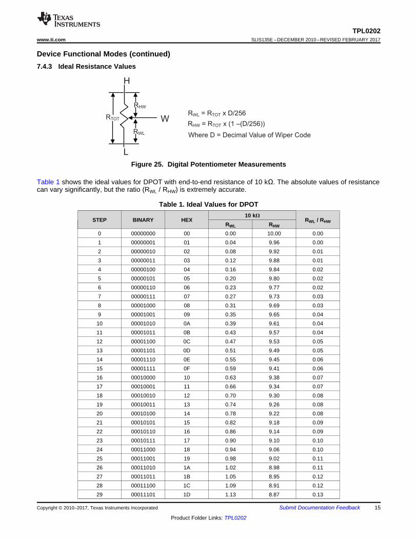
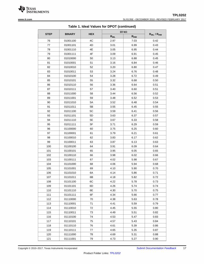
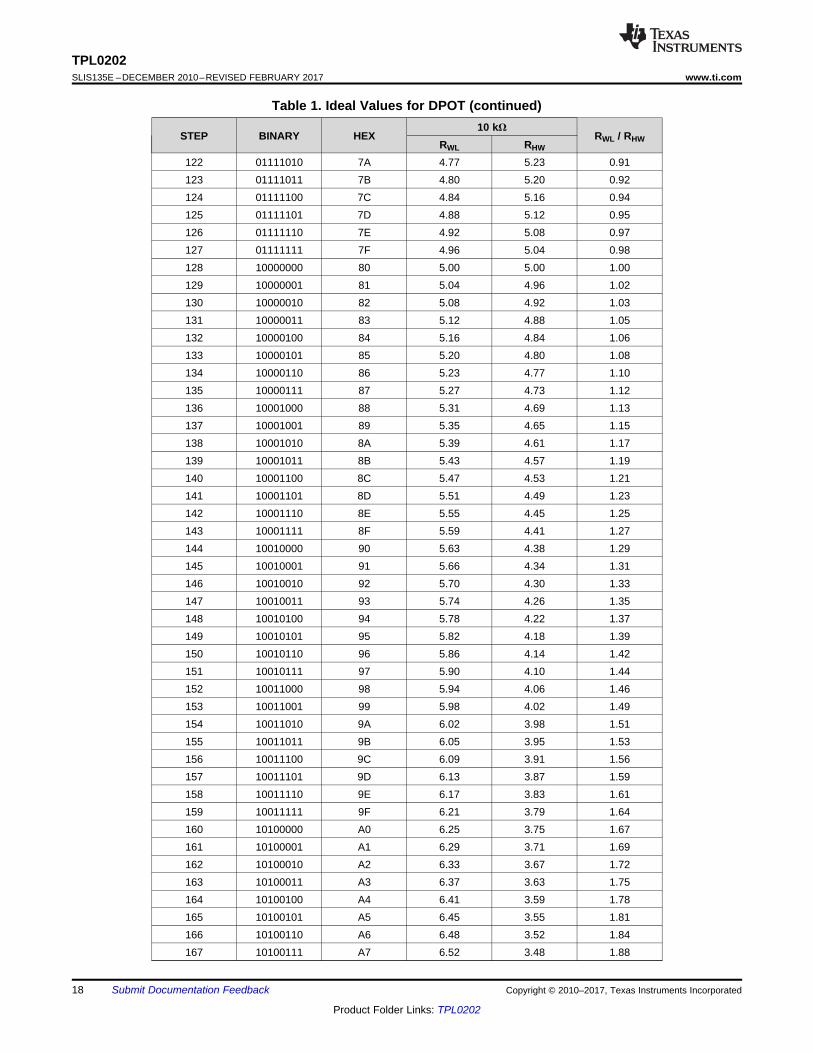
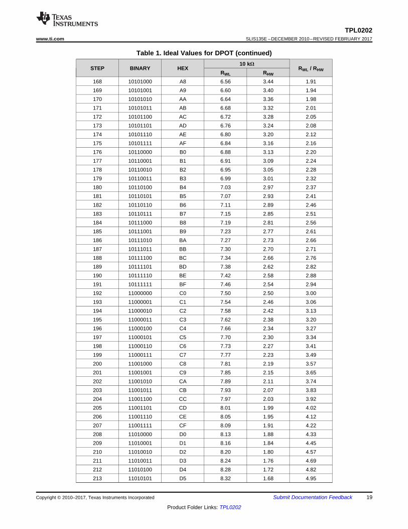
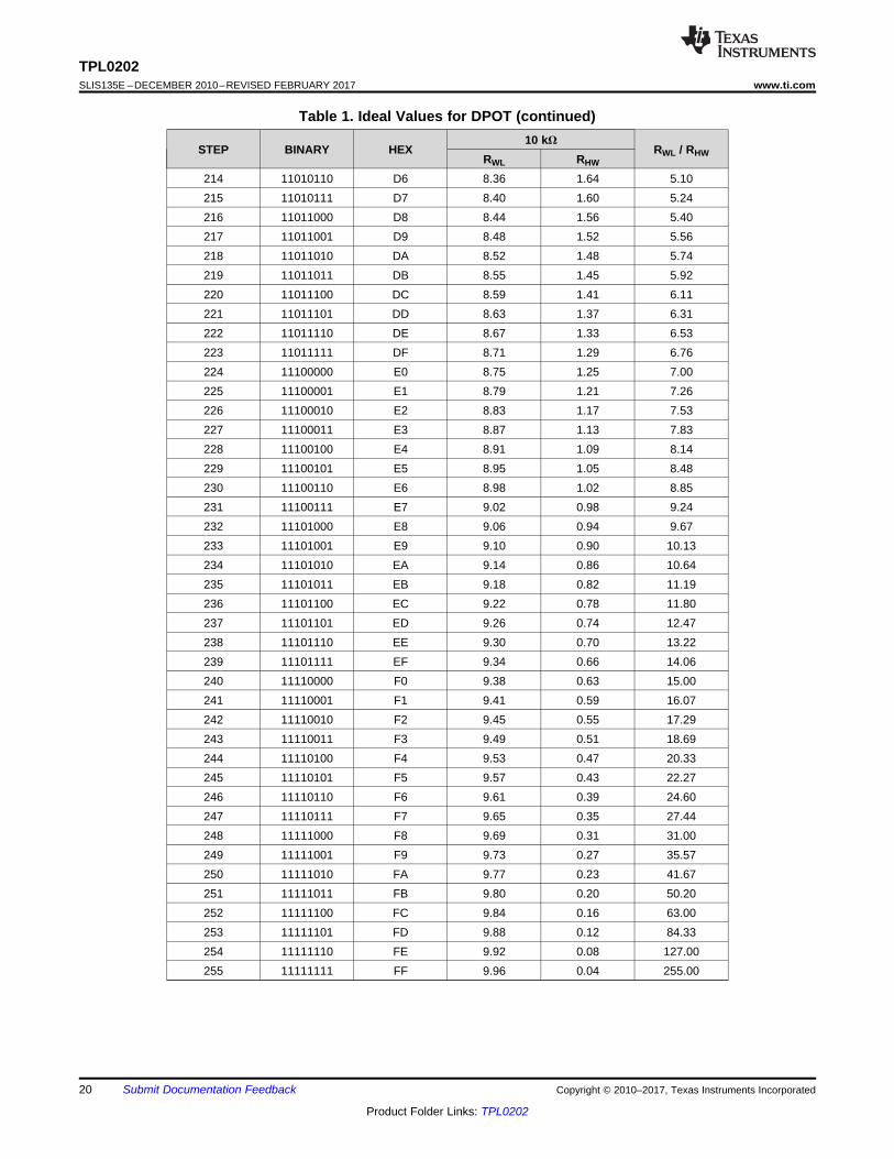
Device Functional Modes (continued)7.4.3 Ideal Resistance Values
Figure 25. Digital Potentiometer Measurements
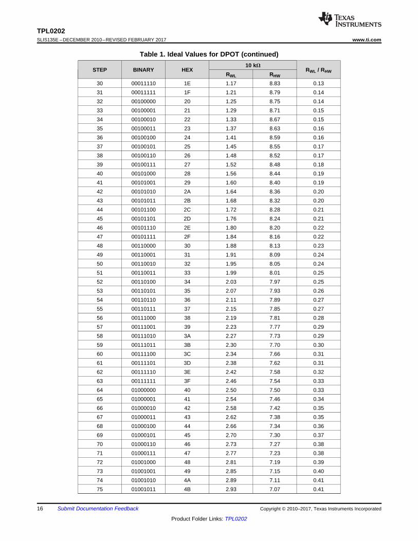
Table 1 shows the ideal values for DPOT with end-to-end resistance of 10 kΩ. The absolute values of resistancecan vary significantly, but the ratio (RWL / RHW) is extremely accurate.
Table 1. Ideal Values for DPOT
STEP BINARY HEX10 kΩ
RWL / RHWRWL RHW
0 00000000 00 0.00 10.00 0.001 00000001 01 0.04 9.96 0.002 00000010 02 0.08 9.92 0.013 00000011 03 0.12 9.88 0.014 00000100 04 0.16 9.84 0.025 00000101 05 0.20 9.80 0.026 00000110 06 0.23 9.77 0.027 00000111 07 0.27 9.73 0.038 00001000 08 0.31 9.69 0.039 00001001 09 0.35 9.65 0.0410 00001010 0A 0.39 9.61 0.0411 00001011 0B 0.43 9.57 0.0412 00001100 0C 0.47 9.53 0.0513 00001101 0D 0.51 9.49 0.0514 00001110 0E 0.55 9.45 0.0615 00001111 0F 0.59 9.41 0.0616 00010000 10 0.63 9.38 0.0717 00010001 11 0.66 9.34 0.0718 00010010 12 0.70 9.30 0.0819 00010011 13 0.74 9.26 0.0820 00010100 14 0.78 9.22 0.0821 00010101 15 0.82 9.18 0.0922 00010110 16 0.86 9.14 0.0923 00010111 17 0.90 9.10 0.1024 00011000 18 0.94 9.06 0.1025 00011001 19 0.98 9.02 0.1126 00011010 1A 1.02 8.98 0.1127 00011011 1B 1.05 8.95 0.1228 00011100 1C 1.09 8.91 0.1229 00011101 1D 1.13 8.87 0.13
16
TPL0202SLIS135E –DECEMBER 2010–REVISED FEBRUARY 2017 www.ti.com
Product Folder Links: TPL0202
Submit Documentation Feedback Copyright © 2010–2017, Texas Instruments Incorporated
Table 1. Ideal Values for DPOT (continued)
STEP BINARY HEX10 kΩ
RWL / RHWRWL RHW
30 00011110 1E 1.17 8.83 0.1331 00011111 1F 1.21 8.79 0.1432 00100000 20 1.25 8.75 0.1433 00100001 21 1.29 8.71 0.1534 00100010 22 1.33 8.67 0.1535 00100011 23 1.37 8.63 0.1636 00100100 24 1.41 8.59 0.1637 00100101 25 1.45 8.55 0.1738 00100110 26 1.48 8.52 0.1739 00100111 27 1.52 8.48 0.1840 00101000 28 1.56 8.44 0.1941 00101001 29 1.60 8.40 0.1942 00101010 2A 1.64 8.36 0.2043 00101011 2B 1.68 8.32 0.2044 00101100 2C 1.72 8.28 0.2145 00101101 2D 1.76 8.24 0.2146 00101110 2E 1.80 8.20 0.2247 00101111 2F 1.84 8.16 0.2248 00110000 30 1.88 8.13 0.2349 00110001 31 1.91 8.09 0.2450 00110010 32 1.95 8.05 0.2451 00110011 33 1.99 8.01 0.2552 00110100 34 2.03 7.97 0.2553 00110101 35 2.07 7.93 0.2654 00110110 36 2.11 7.89 0.2755 00110111 37 2.15 7.85 0.2756 00111000 38 2.19 7.81 0.2857 00111001 39 2.23 7.77 0.2958 00111010 3A 2.27 7.73 0.2959 00111011 3B 2.30 7.70 0.3060 00111100 3C 2.34 7.66 0.3161 00111101 3D 2.38 7.62 0.3162 00111110 3E 2.42 7.58 0.3263 00111111 3F 2.46 7.54 0.3364 01000000 40 2.50 7.50 0.3365 01000001 41 2.54 7.46 0.3466 01000010 42 2.58 7.42 0.3567 01000011 43 2.62 7.38 0.3568 01000100 44 2.66 7.34 0.3669 01000101 45 2.70 7.30 0.3770 01000110 46 2.73 7.27 0.3871 01000111 47 2.77 7.23 0.3872 01001000 48 2.81 7.19 0.3973 01001001 49 2.85 7.15 0.4074 01001010 4A 2.89 7.11 0.4175 01001011 4B 2.93 7.07 0.41
17
TPL0202www.ti.com SLIS135E –DECEMBER 2010–REVISED FEBRUARY 2017
Product Folder Links: TPL0202
Submit Documentation FeedbackCopyright © 2010–2017, Texas Instruments Incorporated
Table 1. Ideal Values for DPOT (continued)
STEP BINARY HEX10 kΩ
RWL / RHWRWL RHW
76 01001100 4C 2.97 7.03 0.4277 01001101 4D 3.01 6.99 0.4378 01001110 4E 3.05 6.95 0.4479 01001111 4F 3.09 6.91 0.4580 01010000 50 3.13 6.88 0.4581 01010001 51 3.16 6.84 0.4682 01010010 52 3.20 6.80 0.4783 01010011 53 3.24 6.76 0.4884 01010100 54 3.28 6.72 0.4985 01010101 55 3.32 6.68 0.5086 01010110 56 3.36 6.64 0.5187 01010111 57 3.40 6.60 0.5188 01011000 58 3.44 6.56 0.5289 01011001 59 3.48 6.52 0.5390 01011010 5A 3.52 6.48 0.5491 01011011 5B 3.55 6.45 0.5592 01011100 5C 3.59 6.41 0.5693 01011101 5D 3.63 6.37 0.5794 01011110 5E 3.67 6.33 0.5895 01011111 5F 3.71 6.29 0.5996 01100000 60 3.75 6.25 0.6097 01100001 61 3.79 6.21 0.6198 01100010 62 3.83 6.17 0.6299 01100011 63 3.87 6.13 0.63100 01100100 64 3.91 6.09 0.64101 01100101 65 3.95 6.05 0.65102 01100110 66 3.98 6.02 0.66103 01100111 67 4.02 5.98 0.67104 01101000 68 4.06 5.94 0.68105 01101001 69 4.10 5.90 0.70106 01101010 6A 4.14 5.86 0.71107 01101011 6B 4.18 5.82 0.72108 01101100 6C 4.22 5.78 0.73109 01101101 6D 4.26 5.74 0.74110 01101110 6E 4.30 5.70 0.75111 01101111 6F 4.34 5.66 0.77112 01110000 70 4.38 5.63 0.78113 01110001 71 4.41 5.59 0.79114 01110010 72 4.45 5.55 0.80115 01110011 73 4.49 5.51 0.82116 01110100 74 4.53 5.47 0.83117 01110101 75 4.57 5.43 0.84118 01110110 76 4.61 5.39 0.86119 01110111 77 4.65 5.35 0.87120 01111000 78 4.69 5.31 0.88121 01111001 79 4.73 5.27 0.90
18
TPL0202SLIS135E –DECEMBER 2010–REVISED FEBRUARY 2017 www.ti.com
Product Folder Links: TPL0202
Submit Documentation Feedback Copyright © 2010–2017, Texas Instruments Incorporated
Table 1. Ideal Values for DPOT (continued)
STEP BINARY HEX10 kΩ
RWL / RHWRWL RHW
122 01111010 7A 4.77 5.23 0.91123 01111011 7B 4.80 5.20 0.92124 01111100 7C 4.84 5.16 0.94125 01111101 7D 4.88 5.12 0.95126 01111110 7E 4.92 5.08 0.97127 01111111 7F 4.96 5.04 0.98128 10000000 80 5.00 5.00 1.00129 10000001 81 5.04 4.96 1.02130 10000010 82 5.08 4.92 1.03131 10000011 83 5.12 4.88 1.05132 10000100 84 5.16 4.84 1.06133 10000101 85 5.20 4.80 1.08134 10000110 86 5.23 4.77 1.10135 10000111 87 5.27 4.73 1.12136 10001000 88 5.31 4.69 1.13137 10001001 89 5.35 4.65 1.15138 10001010 8A 5.39 4.61 1.17139 10001011 8B 5.43 4.57 1.19140 10001100 8C 5.47 4.53 1.21141 10001101 8D 5.51 4.49 1.23142 10001110 8E 5.55 4.45 1.25143 10001111 8F 5.59 4.41 1.27144 10010000 90 5.63 4.38 1.29145 10010001 91 5.66 4.34 1.31146 10010010 92 5.70 4.30 1.33147 10010011 93 5.74 4.26 1.35148 10010100 94 5.78 4.22 1.37149 10010101 95 5.82 4.18 1.39150 10010110 96 5.86 4.14 1.42151 10010111 97 5.90 4.10 1.44152 10011000 98 5.94 4.06 1.46153 10011001 99 5.98 4.02 1.49154 10011010 9A 6.02 3.98 1.51155 10011011 9B 6.05 3.95 1.53156 10011100 9C 6.09 3.91 1.56157 10011101 9D 6.13 3.87 1.59158 10011110 9E 6.17 3.83 1.61159 10011111 9F 6.21 3.79 1.64160 10100000 A0 6.25 3.75 1.67161 10100001 A1 6.29 3.71 1.69162 10100010 A2 6.33 3.67 1.72163 10100011 A3 6.37 3.63 1.75164 10100100 A4 6.41 3.59 1.78165 10100101 A5 6.45 3.55 1.81166 10100110 A6 6.48 3.52 1.84167 10100111 A7 6.52 3.48 1.88
19
TPL0202www.ti.com SLIS135E –DECEMBER 2010–REVISED FEBRUARY 2017
Product Folder Links: TPL0202
Submit Documentation FeedbackCopyright © 2010–2017, Texas Instruments Incorporated
Table 1. Ideal Values for DPOT (continued)
STEP BINARY HEX10 kΩ
RWL / RHWRWL RHW
168 10101000 A8 6.56 3.44 1.91169 10101001 A9 6.60 3.40 1.94170 10101010 AA 6.64 3.36 1.98171 10101011 AB 6.68 3.32 2.01172 10101100 AC 6.72 3.28 2.05173 10101101 AD 6.76 3.24 2.08174 10101110 AE 6.80 3.20 2.12175 10101111 AF 6.84 3.16 2.16176 10110000 B0 6.88 3.13 2.20177 10110001 B1 6.91 3.09 2.24178 10110010 B2 6.95 3.05 2.28179 10110011 B3 6.99 3.01 2.32180 10110100 B4 7.03 2.97 2.37181 10110101 B5 7.07 2.93 2.41182 10110110 B6 7.11 2.89 2.46183 10110111 B7 7.15 2.85 2.51184 10111000 B8 7.19 2.81 2.56185 10111001 B9 7.23 2.77 2.61186 10111010 BA 7.27 2.73 2.66187 10111011 BB 7.30 2.70 2.71188 10111100 BC 7.34 2.66 2.76189 10111101 BD 7.38 2.62 2.82190 10111110 BE 7.42 2.58 2.88191 10111111 BF 7.46 2.54 2.94192 11000000 C0 7.50 2.50 3.00193 11000001 C1 7.54 2.46 3.06194 11000010 C2 7.58 2.42 3.13195 11000011 C3 7.62 2.38 3.20196 11000100 C4 7.66 2.34 3.27197 11000101 C5 7.70 2.30 3.34198 11000110 C6 7.73 2.27 3.41199 11000111 C7 7.77 2.23 3.49200 11001000 C8 7.81 2.19 3.57201 11001001 C9 7.85 2.15 3.65202 11001010 CA 7.89 2.11 3.74203 11001011 CB 7.93 2.07 3.83204 11001100 CC 7.97 2.03 3.92205 11001101 CD 8.01 1.99 4.02206 11001110 CE 8.05 1.95 4.12207 11001111 CF 8.09 1.91 4.22208 11010000 D0 8.13 1.88 4.33209 11010001 D1 8.16 1.84 4.45210 11010010 D2 8.20 1.80 4.57211 11010011 D3 8.24 1.76 4.69212 11010100 D4 8.28 1.72 4.82213 11010101 D5 8.32 1.68 4.95
20
TPL0202SLIS135E –DECEMBER 2010–REVISED FEBRUARY 2017 www.ti.com
Product Folder Links: TPL0202
Submit Documentation Feedback Copyright © 2010–2017, Texas Instruments Incorporated
Table 1. Ideal Values for DPOT (continued)
STEP BINARY HEX10 kΩ
RWL / RHWRWL RHW
214 11010110 D6 8.36 1.64 5.10215 11010111 D7 8.40 1.60 5.24216 11011000 D8 8.44 1.56 5.40217 11011001 D9 8.48 1.52 5.56218 11011010 DA 8.52 1.48 5.74219 11011011 DB 8.55 1.45 5.92220 11011100 DC 8.59 1.41 6.11221 11011101 DD 8.63 1.37 6.31222 11011110 DE 8.67 1.33 6.53223 11011111 DF 8.71 1.29 6.76224 11100000 E0 8.75 1.25 7.00225 11100001 E1 8.79 1.21 7.26226 11100010 E2 8.83 1.17 7.53227 11100011 E3 8.87 1.13 7.83228 11100100 E4 8.91 1.09 8.14229 11100101 E5 8.95 1.05 8.48230 11100110 E6 8.98 1.02 8.85231 11100111 E7 9.02 0.98 9.24232 11101000 E8 9.06 0.94 9.67233 11101001 E9 9.10 0.90 10.13234 11101010 EA 9.14 0.86 10.64235 11101011 EB 9.18 0.82 11.19236 11101100 EC 9.22 0.78 11.80237 11101101 ED 9.26 0.74 12.47238 11101110 EE 9.30 0.70 13.22239 11101111 EF 9.34 0.66 14.06240 11110000 F0 9.38 0.63 15.00241 11110001 F1 9.41 0.59 16.07242 11110010 F2 9.45 0.55 17.29243 11110011 F3 9.49 0.51 18.69244 11110100 F4 9.53 0.47 20.33245 11110101 F5 9.57 0.43 22.27246 11110110 F6 9.61 0.39 24.60247 11110111 F7 9.65 0.35 27.44248 11111000 F8 9.69 0.31 31.00249 11111001 F9 9.73 0.27 35.57250 11111010 FA 9.77 0.23 41.67251 11111011 FB 9.80 0.20 50.20252 11111100 FC 9.84 0.16 63.00253 11111101 FD 9.88 0.12 84.33254 11111110 FE 9.92 0.08 127.00255 11111111 FF 9.96 0.04 255.00
SCLK
DIN
tCS0
tCSS
tDS
tSCL tSCH
tDH
tSCP tCSH
tCSW
tCS1
CS
SCLK
DIN
1 2 3 4 5 6 7 8 9 10 11 12 13 14 15 16
C1 C0 A1 A0 D7 D6 D5 D4 D3 D2 D1 D0
SCLK
DIN
1 2 3 4 5 6 7 8
C1 C0 A1 A0
A) 16-clock cycle Data Write Sequence
B) 8-clock cycle Data Move/Copy Sequence
CS
CS
21
TPL0202www.ti.com SLIS135E –DECEMBER 2010–REVISED FEBRUARY 2017
Product Folder Links: TPL0202
Submit Documentation FeedbackCopyright © 2010–2017, Texas Instruments Incorporated
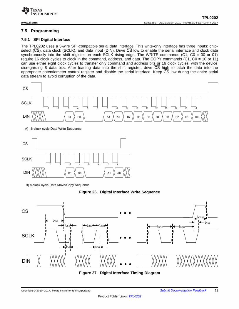
7.5 Programming
7.5.1 SPI Digital InterfaceThe TPL0202 uses a 3-wire SPI-compatible serial data interface. This write-only interface has three inputs: chip-select (CS), data clock (SCLK), and data input (DIN). Drive CS low to enable the serial interface and clock datasynchronously into the shift register on each SCLK rising edge. The WRITE commands (C1, C0 = 00 or 01)require 16 clock cycles to clock in the command, address, and data. The COPY commands (C1, C0 = 10 or 11)can use either eight clock cycles to transfer only command and address bits or 16 clock cycles, with the devicedisregarding 8 data bits. After loading data into the shift register, drive CS high to latch the data into theappropriate potentiometer control register and disable the serial interface. Keep CS low during the entire serialdata stream to avoid corruption of the data.
Figure 26. Digital Interface Write Sequence
Figure 27. Digital Interface Timing Diagram
22
TPL0202SLIS135E –DECEMBER 2010–REVISED FEBRUARY 2017 www.ti.com
Product Folder Links: TPL0202
Submit Documentation Feedback Copyright © 2010–2017, Texas Instruments Incorporated
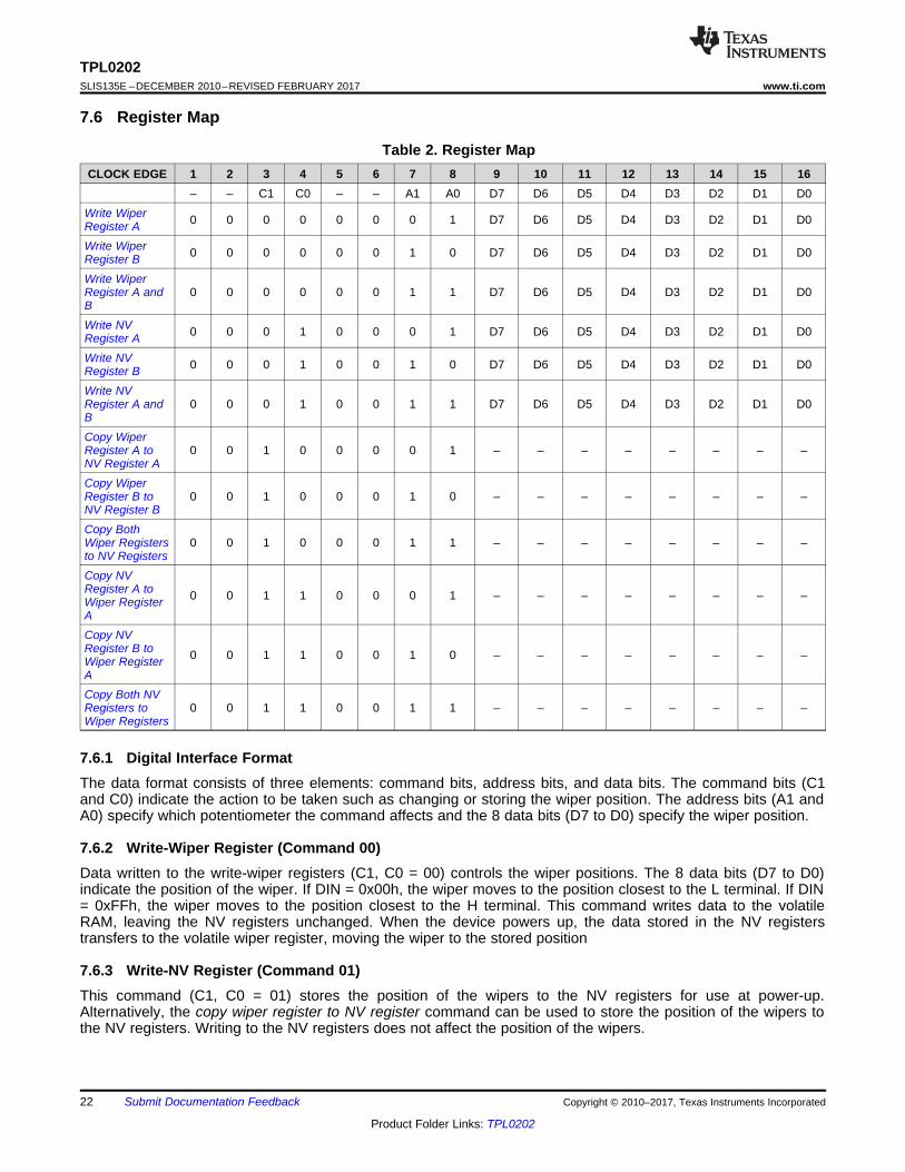
7.6 Register Map
Table 2. Register MapCLOCK EDGE 1 2 3 4 5 6 7 8 9 10 11 12 13 14 15 16
– – C1 C0 – – A1 A0 D7 D6 D5 D4 D3 D2 D1 D0Write WiperRegister A 0 0 0 0 0 0 0 1 D7 D6 D5 D4 D3 D2 D1 D0
Write WiperRegister B 0 0 0 0 0 0 1 0 D7 D6 D5 D4 D3 D2 D1 D0
Write WiperRegister A andB
0 0 0 0 0 0 1 1 D7 D6 D5 D4 D3 D2 D1 D0
Write NVRegister A 0 0 0 1 0 0 0 1 D7 D6 D5 D4 D3 D2 D1 D0
Write NVRegister B 0 0 0 1 0 0 1 0 D7 D6 D5 D4 D3 D2 D1 D0
Write NVRegister A andB
0 0 0 1 0 0 1 1 D7 D6 D5 D4 D3 D2 D1 D0
Copy WiperRegister A toNV Register A
0 0 1 0 0 0 0 1 – – – – – – – –
Copy WiperRegister B toNV Register B
0 0 1 0 0 0 1 0 – – – – – – – –
Copy BothWiper Registersto NV Registers
0 0 1 0 0 0 1 1 – – – – – – – –
Copy NVRegister A toWiper RegisterA
0 0 1 1 0 0 0 1 – – – – – – – –
Copy NVRegister B toWiper RegisterA
0 0 1 1 0 0 1 0 – – – – – – – –
Copy Both NVRegisters toWiper Registers
0 0 1 1 0 0 1 1 – – – – – – – –
7.6.1 Digital Interface FormatThe data format consists of three elements: command bits, address bits, and data bits. The command bits (C1and C0) indicate the action to be taken such as changing or storing the wiper position. The address bits (A1 andA0) specify which potentiometer the command affects and the 8 data bits (D7 to D0) specify the wiper position.
7.6.2 Write-Wiper Register (Command 00)Data written to the write-wiper registers (C1, C0 = 00) controls the wiper positions. The 8 data bits (D7 to D0)indicate the position of the wiper. If DIN = 0x00h, the wiper moves to the position closest to the L terminal. If DIN= 0xFFh, the wiper moves to the position closest to the H terminal. This command writes data to the volatileRAM, leaving the NV registers unchanged. When the device powers up, the data stored in the NV registerstransfers to the volatile wiper register, moving the wiper to the stored position
7.6.3 Write-NV Register (Command 01)This command (C1, C0 = 01) stores the position of the wipers to the NV registers for use at power-up.Alternatively, the copy wiper register to NV register command can be used to store the position of the wipers tothe NV registers. Writing to the NV registers does not affect the position of the wipers.

23
TPL0202www.ti.com SLIS135E –DECEMBER 2010–REVISED FEBRUARY 2017
Product Folder Links: TPL0202
Submit Documentation FeedbackCopyright © 2010–2017, Texas Instruments Incorporated
7.6.4 Copy Wiper Register to NV Register (Command 10)This command (C1, C0 = 10) stores the current position of the wiper to the NV register, for use at power-up. Thiscommand may affect one potentiometer at a time, or both simultaneously, depending on the state of A1 and A0.Alternatively, the write NV register command can be used to store the current position of the wiper to the NVregister.
7.6.5 Copy NV Register to Wiper Register (Command 11)This command (C1, C0 = 11) restores the wiper position to the previously stored position in the NV register. Thiscommand may affect one potentiometer at a time, or both simultaneously, depending on the state of A1 and A0.
Vo
Vi
10 N
Vcc
TPL0202
OPA320
H
W
L
24
TPL0202SLIS135E –DECEMBER 2010–REVISED FEBRUARY 2017 www.ti.com
Product Folder Links: TPL0202
Submit Documentation Feedback Copyright © 2010–2017, Texas Instruments Incorporated
8 Application and Implementation
NOTEInformation in the following applications sections is not part of the TI componentspecification, and TI does not warrant its accuracy or completeness. TI’s customers areresponsible for determining suitability of components for their purposes. Customers shouldvalidate and test their design implementation to confirm system functionality.
8.1 Application InformationMany applications require using a digital potentiometer such as the TPL0202 for variable resistance or voltagedivision; the following application shows a few examples. In conjunction with various amplifiers, the TPL0202 caneffectively be used in rheostat mode to modify the gain of an amplifier, in voltage divider mode to create a digital-to-analog converter (DAC), or one of the potentiometers can be used in voltage divider mode while the other is inrheostat mode to create a variable current sink.
Digital potentiometers have additional use cases. See the Related Documentation section for additionalresources that have application examples including adjustable current source and gain adjustment.
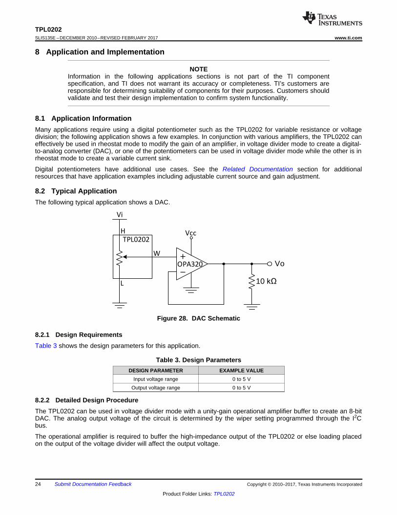
8.2 Typical ApplicationThe following typical application shows a DAC.
Figure 28. DAC Schematic
8.2.1 Design RequirementsTable 3 shows the design parameters for this application.
Table 3. Design ParametersDESIGN PARAMETER EXAMPLE VALUE
Input voltage range 0 to 5 VOutput voltage range 0 to 5 V
8.2.2 Detailed Design ProcedureThe TPL0202 can be used in voltage divider mode with a unity-gain operational amplifier buffer to create an 8-bitDAC. The analog output voltage of the circuit is determined by the wiper setting programmed through the I2Cbus.
The operational amplifier is required to buffer the high-impedance output of the TPL0202 or else loading placedon the output of the voltage divider will affect the output voltage.
Code (Digital Input)
Out
put V
olta
ge (
V)
0 30 60 90 120 150 180 210 240 2560
1
2
3
4
5
6
D001
5 V2.7 V
25
TPL0202www.ti.com SLIS135E –DECEMBER 2010–REVISED FEBRUARY 2017
Product Folder Links: TPL0202
Submit Documentation FeedbackCopyright © 2010–2017, Texas Instruments Incorporated
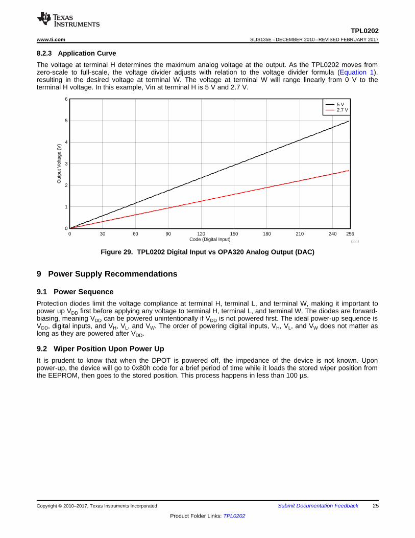
8.2.3 Application CurveThe voltage at terminal H determines the maximum analog voltage at the output. As the TPL0202 moves fromzero-scale to full-scale, the voltage divider adjusts with relation to the voltage divider formula (Equation 1),resulting in the desired voltage at terminal W. The voltage at terminal W will range linearly from 0 V to theterminal H voltage. In this example, Vin at terminal H is 5 V and 2.7 V.
Figure 29. TPL0202 Digital Input vs OPA320 Analog Output (DAC)
9 Power Supply Recommendations
9.1 Power SequenceProtection diodes limit the voltage compliance at terminal H, terminal L, and terminal W, making it important topower up VDD first before applying any voltage to terminal H, terminal L, and terminal W. The diodes are forward-biasing, meaning VDD can be powered unintentionally if VDD is not powered first. The ideal power-up sequence isVDD, digital inputs, and VH, VL, and VW. The order of powering digital inputs, VH, VL, and VW does not matter aslong as they are powered after VDD.
9.2 Wiper Position Upon Power UpIt is prudent to know that when the DPOT is powered off, the impedance of the device is not known. Uponpower-up, the device will go to 0x80h code for a brief period of time while it loads the stored wiper position fromthe EEPROM, then goes to the stored position. This process happens in less than 100 µs.
DIN
SC
LK
CS
GND
VD
D
HA
0603 Cap
0402
Cap
Vo
lta
ge
Div
ide
r O
utp
ut
Via to GND Plane
Via to VDD Power Plane
1
LA
WA
HBWBLB
Rh
eo
sta
t O
utp
ut
A
Rh
eo
sta
t O
utp
ut
B
26
TPL0202SLIS135E –DECEMBER 2010–REVISED FEBRUARY 2017 www.ti.com
Product Folder Links: TPL0202
Submit Documentation Feedback Copyright © 2010–2017, Texas Instruments Incorporated
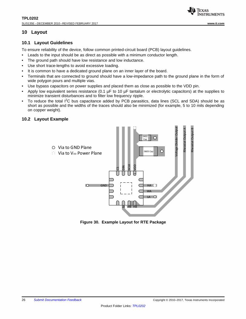
10 Layout
10.1 Layout GuidelinesTo ensure reliability of the device, follow common printed-circuit board (PCB) layout guidelines.• Leads to the input should be as direct as possible with a minimum conductor length.• The ground path should have low resistance and low inductance.• Use short trace-lengths to avoid excessive loading.• It is common to have a dedicated ground plane on an inner layer of the board.• Terminals that are connected to ground should have a low-impedance path to the ground plane in the form of
wide polygon pours and multiple vias.• Use bypass capacitors on power supplies and placed them as close as possible to the VDD pin.• Apply low equivalent series resistance (0.1 µF to 10 µF tantalum or electrolytic capacitors) at the supplies to
minimize transient disturbances and to filter low frequency ripple.• To reduce the total I2C bus capacitance added by PCB parasitics, data lines (SCL and SDA) should be as
short as possible and the widths of the traces should also be minimized (for example, 5 to 10 mils dependingon copper weight).
10.2 Layout Example
Figure 30. Example Layout for RTE Package
27
TPL0202www.ti.com SLIS135E –DECEMBER 2010–REVISED FEBRUARY 2017
Product Folder Links: TPL0202
Submit Documentation FeedbackCopyright © 2010–2017, Texas Instruments Incorporated
11 Device and Documentation Support
11.1 Documentation Support
11.1.1 Related DocumentationFor related documentation see the following:
TPL0102 Two 256-Taps Digital Potentiometers With Non-Volatile Memory (SLIS134)
11.2 Receiving Notification of Documentation UpdatesTo receive notification of documentation updates, navigate to the device product folder on ti.com. In the upperright corner, click on Alert me to register and receive a weekly digest of any product information that haschanged. For change details, review the revision history included in any revised document.
11.3 Community ResourcesThe following links connect to TI community resources. Linked contents are provided "AS IS" by the respectivecontributors. They do not constitute TI specifications and do not necessarily reflect TI's views; see TI's Terms ofUse.
TI E2E™ Online Community TI's Engineer-to-Engineer (E2E) Community. Created to foster collaborationamong engineers. At e2e.ti.com, you can ask questions, share knowledge, explore ideas and helpsolve problems with fellow engineers.
Design Support TI's Design Support Quickly find helpful E2E forums along with design support tools andcontact information for technical support.
11.4 TrademarksE2E is a trademark of Texas Instruments.All other trademarks are the property of their respective owners.
11.5 Electrostatic Discharge CautionThese devices have limited built-in ESD protection. The leads should be shorted together or the device placed in conductive foamduring storage or handling to prevent electrostatic damage to the MOS gates.
11.6 GlossarySLYZ022 — TI Glossary.
This glossary lists and explains terms, acronyms, and definitions.
12 Mechanical, Packaging, and Orderable InformationThe following pages include mechanical, packaging, and orderable information. This information is the mostcurrent data available for the designated devices. This data is subject to change without notice and revision ofthis document. For browser-based versions of this data sheet, refer to the left-hand navigation.
PACKAGE OPTION ADDENDUM
www.ti.com 24-Jan-2017
Addendum-Page 1
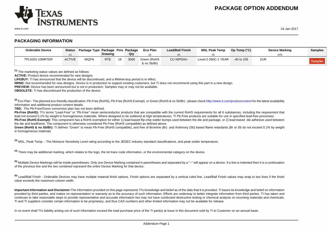
PACKAGING INFORMATION
Orderable Device Status(1)
Package Type PackageDrawing
Pins PackageQty
Eco Plan(2)
Lead/Ball Finish(6)
MSL Peak Temp(3)
Op Temp (°C) Device Marking(4/5)
Samples
TPL0202-10MRTER ACTIVE WQFN RTE 16 3000 Green (RoHS& no Sb/Br)
CU NIPDAU Level-2-260C-1 YEAR -40 to 105 ZUR
(1) The marketing status values are defined as follows:ACTIVE: Product device recommended for new designs.LIFEBUY: TI has announced that the device will be discontinued, and a lifetime-buy period is in effect.NRND: Not recommended for new designs. Device is in production to support existing customers, but TI does not recommend using this part in a new design.PREVIEW: Device has been announced but is not in production. Samples may or may not be available.OBSOLETE: TI has discontinued the production of the device.
(2) Eco Plan - The planned eco-friendly classification: Pb-Free (RoHS), Pb-Free (RoHS Exempt), or Green (RoHS & no Sb/Br) - please check http://www.ti.com/productcontent for the latest availabilityinformation and additional product content details.TBD: The Pb-Free/Green conversion plan has not been defined.Pb-Free (RoHS): TI's terms "Lead-Free" or "Pb-Free" mean semiconductor products that are compatible with the current RoHS requirements for all 6 substances, including the requirement thatlead not exceed 0.1% by weight in homogeneous materials. Where designed to be soldered at high temperatures, TI Pb-Free products are suitable for use in specified lead-free processes.Pb-Free (RoHS Exempt): This component has a RoHS exemption for either 1) lead-based flip-chip solder bumps used between the die and package, or 2) lead-based die adhesive used betweenthe die and leadframe. The component is otherwise considered Pb-Free (RoHS compatible) as defined above.Green (RoHS & no Sb/Br): TI defines "Green" to mean Pb-Free (RoHS compatible), and free of Bromine (Br) and Antimony (Sb) based flame retardants (Br or Sb do not exceed 0.1% by weightin homogeneous material)
(3) MSL, Peak Temp. - The Moisture Sensitivity Level rating according to the JEDEC industry standard classifications, and peak solder temperature.
(4) There may be additional marking, which relates to the logo, the lot trace code information, or the environmental category on the device.
(5) Multiple Device Markings will be inside parentheses. Only one Device Marking contained in parentheses and separated by a "~" will appear on a device. If a line is indented then it is a continuationof the previous line and the two combined represent the entire Device Marking for that device.
(6) Lead/Ball Finish - Orderable Devices may have multiple material finish options. Finish options are separated by a vertical ruled line. Lead/Ball Finish values may wrap to two lines if the finishvalue exceeds the maximum column width.
Important Information and Disclaimer:The information provided on this page represents TI's knowledge and belief as of the date that it is provided. TI bases its knowledge and belief on informationprovided by third parties, and makes no representation or warranty as to the accuracy of such information. Efforts are underway to better integrate information from third parties. TI has taken andcontinues to take reasonable steps to provide representative and accurate information but may not have conducted destructive testing or chemical analysis on incoming materials and chemicals.TI and TI suppliers consider certain information to be proprietary, and thus CAS numbers and other limited information may not be available for release.
In no event shall TI's liability arising out of such information exceed the total purchase price of the TI part(s) at issue in this document sold by TI to Customer on an annual basis.
PACKAGE OPTION ADDENDUM
www.ti.com 24-Jan-2017
Addendum-Page 2
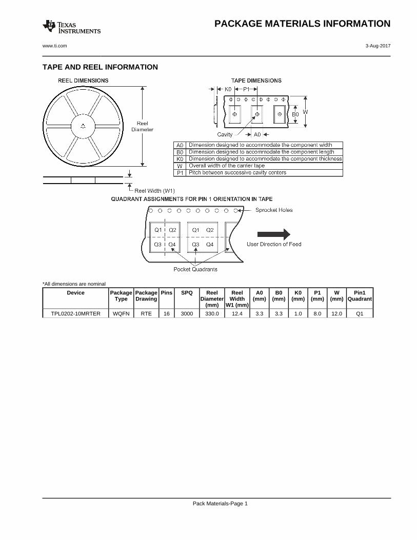
TAPE AND REEL INFORMATION
*All dimensions are nominal
Device PackageType
PackageDrawing
Pins SPQ ReelDiameter
(mm)
ReelWidth
W1 (mm)
A0(mm)
B0(mm)
K0(mm)
P1(mm)
W(mm)
Pin1Quadrant
TPL0202-10MRTER WQFN RTE 16 3000 330.0 12.4 3.3 3.3 1.0 8.0 12.0 Q1
PACKAGE MATERIALS INFORMATION
www.ti.com 3-Aug-2017
Pack Materials-Page 1
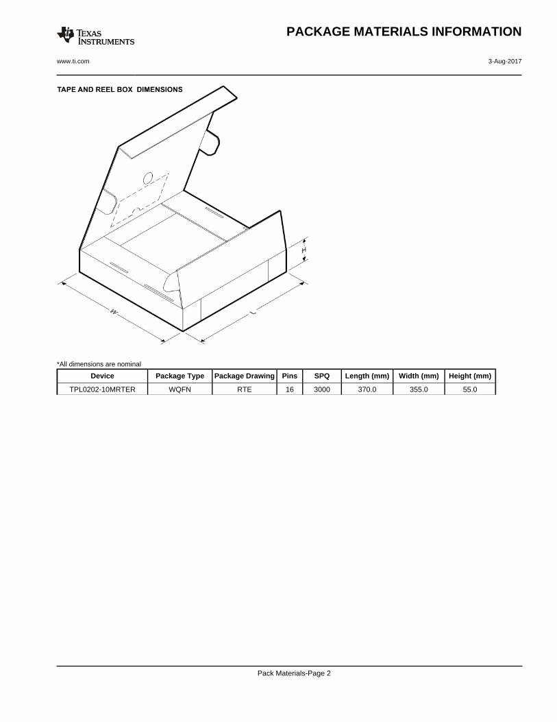
*All dimensions are nominal
Device Package Type Package Drawing Pins SPQ Length (mm) Width (mm) Height (mm)
TPL0202-10MRTER WQFN RTE 16 3000 370.0 355.0 55.0
PACKAGE MATERIALS INFORMATION
www.ti.com 3-Aug-2017
Pack Materials-Page 2
IMPORTANT NOTICE
Texas Instruments Incorporated (TI) reserves the right to make corrections, enhancements, improvements and other changes to itssemiconductor products and services per JESD46, latest issue, and to discontinue any product or service per JESD48, latest issue. Buyersshould obtain the latest relevant information before placing orders and should verify that such information is current and complete.TI’s published terms of sale for semiconductor products (http://www.ti.com/sc/docs/stdterms.htm) apply to the sale of packaged integratedcircuit products that TI has qualified and released to market. Additional terms may apply to the use or sale of other types of TI products andservices.Reproduction of significant portions of TI information in TI data sheets is permissible only if reproduction is without alteration and isaccompanied by all associated warranties, conditions, limitations, and notices. TI is not responsible or liable for such reproduceddocumentation. Information of third parties may be subject to additional restrictions. Resale of TI products or services with statementsdifferent from or beyond the parameters stated by TI for that product or service voids all express and any implied warranties for theassociated TI product or service and is an unfair and deceptive business practice. TI is not responsible or liable for any such statements.Buyers and others who are developing systems that incorporate TI products (collectively, “Designers”) understand and agree that Designersremain responsible for using their independent analysis, evaluation and judgment in designing their applications and that Designers havefull and exclusive responsibility to assure the safety of Designers' applications and compliance of their applications (and of all TI productsused in or for Designers’ applications) with all applicable regulations, laws and other applicable requirements. Designer represents that, withrespect to their applications, Designer has all the necessary expertise to create and implement safeguards that (1) anticipate dangerousconsequences of failures, (2) monitor failures and their consequences, and (3) lessen the likelihood of failures that might cause harm andtake appropriate actions. Designer agrees that prior to using or distributing any applications that include TI products, Designer willthoroughly test such applications and the functionality of such TI products as used in such applications.TI’s provision of technical, application or other design advice, quality characterization, reliability data or other services or information,including, but not limited to, reference designs and materials relating to evaluation modules, (collectively, “TI Resources”) are intended toassist designers who are developing applications that incorporate TI products; by downloading, accessing or using TI Resources in anyway, Designer (individually or, if Designer is acting on behalf of a company, Designer’s company) agrees to use any particular TI Resourcesolely for this purpose and subject to the terms of this Notice.TI’s provision of TI Resources does not expand or otherwise alter TI’s applicable published warranties or warranty disclaimers for TIproducts, and no additional obligations or liabilities arise from TI providing such TI Resources. TI reserves the right to make corrections,enhancements, improvements and other changes to its TI Resources. TI has not conducted any testing other than that specificallydescribed in the published documentation for a particular TI Resource.Designer is authorized to use, copy and modify any individual TI Resource only in connection with the development of applications thatinclude the TI product(s) identified in such TI Resource. NO OTHER LICENSE, EXPRESS OR IMPLIED, BY ESTOPPEL OR OTHERWISETO ANY OTHER TI INTELLECTUAL PROPERTY RIGHT, AND NO LICENSE TO ANY TECHNOLOGY OR INTELLECTUAL PROPERTYRIGHT OF TI OR ANY THIRD PARTY IS GRANTED HEREIN, including but not limited to any patent right, copyright, mask work right, orother intellectual property right relating to any combination, machine, or process in which TI products or services are used. Informationregarding or referencing third-party products or services does not constitute a license to use such products or services, or a warranty orendorsement thereof. Use of TI Resources may require a license from a third party under the patents or other intellectual property of thethird party, or a license from TI under the patents or other intellectual property of TI.TI RESOURCES ARE PROVIDED “AS IS” AND WITH ALL FAULTS. TI DISCLAIMS ALL OTHER WARRANTIES ORREPRESENTATIONS, EXPRESS OR IMPLIED, REGARDING RESOURCES OR USE THEREOF, INCLUDING BUT NOT LIMITED TOACCURACY OR COMPLETENESS, TITLE, ANY EPIDEMIC FAILURE WARRANTY AND ANY IMPLIED WARRANTIES OFMERCHANTABILITY, FITNESS FOR A PARTICULAR PURPOSE, AND NON-INFRINGEMENT OF ANY THIRD PARTY INTELLECTUALPROPERTY RIGHTS. TI SHALL NOT BE LIABLE FOR AND SHALL NOT DEFEND OR INDEMNIFY DESIGNER AGAINST ANY CLAIM,INCLUDING BUT NOT LIMITED TO ANY INFRINGEMENT CLAIM THAT RELATES TO OR IS BASED ON ANY COMBINATION OFPRODUCTS EVEN IF DESCRIBED IN TI RESOURCES OR OTHERWISE. IN NO EVENT SHALL TI BE LIABLE FOR ANY ACTUAL,DIRECT, SPECIAL, COLLATERAL, INDIRECT, PUNITIVE, INCIDENTAL, CONSEQUENTIAL OR EXEMPLARY DAMAGES INCONNECTION WITH OR ARISING OUT OF TI RESOURCES OR USE THEREOF, AND REGARDLESS OF WHETHER TI HAS BEENADVISED OF THE POSSIBILITY OF SUCH DAMAGES.Unless TI has explicitly designated an individual product as meeting the requirements of a particular industry standard (e.g., ISO/TS 16949and ISO 26262), TI is not responsible for any failure to meet such industry standard requirements.Where TI specifically promotes products as facilitating functional safety or as compliant with industry functional safety standards, suchproducts are intended to help enable customers to design and create their own applications that meet applicable functional safety standardsand requirements. Using products in an application does not by itself establish any safety features in the application. Designers mustensure compliance with safety-related requirements and standards applicable to their applications. Designer may not use any TI products inlife-critical medical equipment unless authorized officers of the parties have executed a special contract specifically governing such use.Life-critical medical equipment is medical equipment where failure of such equipment would cause serious bodily injury or death (e.g., lifesupport, pacemakers, defibrillators, heart pumps, neurostimulators, and implantables). Such equipment includes, without limitation, allmedical devices identified by the U.S. Food and Drug Administration as Class III devices and equivalent classifications outside the U.S.TI may expressly designate certain products as completing a particular qualification (e.g., Q100, Military Grade, or Enhanced Product).Designers agree that it has the necessary expertise to select the product with the appropriate qualification designation for their applicationsand that proper product selection is at Designers’ own risk. Designers are solely responsible for compliance with all legal and regulatoryrequirements in connection with such selection.Designer will fully indemnify TI and its representatives against any damages, costs, losses, and/or liabilities arising out of Designer’s non-compliance with the terms and provisions of this Notice.
Mailing Address: Texas Instruments, Post Office Box 655303, Dallas, Texas 75265Copyright © 2017, Texas Instruments Incorporated


![[XLS]sdmylife.comsdmylife.com/files/Master_Course_List_08.27.14.xlsx · Web view3. 3. 1. 1.5. 3. 3. 1.5. 1.5. 1.5. 1.5. 1.5. 1.5. 1.5. 3. 1.5. 3. 3. 3. 1.5. 1.5. 2. 3. 3. 1.5. 1.5](https://img.pdfslide.net/doc/110x75/5ac153d87f8b9a213f8cf61b/xls-view3-3-1-15-3-3-15-15-15-15-15-15-15-3-15-3-3-3.jpg)


![Signatur Notizen - uni-due.de · 1.5 "A-B-C" [1] 1.5 "AC Test" [1] 1.5 ABAT [1] ABAT 1.5 "Mechanic" [1] 1.5 BOT 8-10 [1] BOT 8-10](https://img.pdfslide.net/doc/110x75/5d50f7c588c993127e8b9b77/signatur-notizen-uni-duede-15-a-b-c-1-15-ac-test-1-15-abat-1.jpg)