Embed Size (px)
Citation preview
VIN (V)
RO
N (
m:
)
1.05 1.55 2.05 2.55 3.05 3.55 4.05 4.55 5.05 5.520
30
40
50
60
70
80
D005
-40°C 25°C 85°C105°C
Power Supply
OFF
ON
TPS22914/15
VIN VOUT
RLCL
GND
ON GNDCIN
Product
Folder
Sample &Buy
Technical
Documents
Tools &
Software
Support &Community
An IMPORTANT NOTICE at the end of this data sheet addresses availability, warranty, changes, use in safety-critical applications,intellectual property matters and other important disclaimers. PRODUCTION DATA.
TPS22914B, TPS22914C, TPS22915B, TPS22915CSLVSCO0D –JUNE 2014–REVISED SEPTEMBER 2016
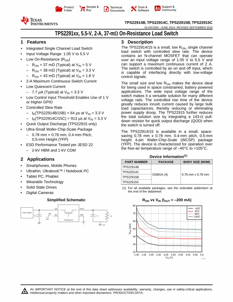
TPS2291xx, 5.5-V, 2-A, 37-mΩ On-Resistance Load Switch
1
1 Features1• Integrated Single Channel Load Switch• Input Voltage Range: 1.05 V to 5.5 V• Low On-Resistance (RON)
– RON = 37 mΩ (Typical) at VIN = 5 V– RON = 38 mΩ (Typical) at VIN = 3.3 V– RON = 43 mΩ (Typical) at VIN = 1.8 V
• 2-A Maximum Continuous Switch Current• Low Quiescent Current
– 7.7 µA (Typical) at VIN = 3.3 V• Low Control Input Threshold Enables Use of 1 V
or Higher GPIO• Controlled Slew Rate
– tR(TPS22914B/15B) = 64 µs at VIN = 3.3 V– tR(TPS22914C/15C) = 913 µs at VIN = 3.3 V
• Quick Output Discharge (TPS22915 only)• Ultra-Small Wafer-Chip-Scale Package
– 0.78 mm × 0.78 mm, 0.4-mm Pitch,0.5-mm Height (YFP)
• ESD Performance Tested per JESD 22– 2-kV HBM and 1-kV CDM
2 Applications• Smartphones, Mobile Phones• Ultrathin, Ultrabook™ / Notebook PC• Tablet PC, Phablet• Wearable Technology• Solid State Drives• Digital Cameras
3 DescriptionThe TPS22914/15 is a small, low RON, single channelload switch with controlled slew rate. The devicecontains an N-channel MOSFET that can operateover an input voltage range of 1.05 V to 5.5 V andcan support a maximum continuous current of 2 A.The switch is controlled by an on and off input, whichis capable of interfacing directly with low-voltagecontrol signals.
The small size and low RON makes the device idealfor being used in space constrained, battery poweredapplications. The wide input voltage range of theswitch makes it a versatile solution for many differentvoltage rails. The controlled rise time of the devicegreatly reduces inrush current caused by large bulkload capacitances, thereby reducing or eliminatingpower supply droop. The TPS22915 further reducesthe total solution size by integrating a 143-Ω pull-down resistor for quick output discharge (QOD) whenthe switch is turned off.
The TPS22914/15 is available in a small, space-saving 0.78 mm x 0.78 mm, 0.4-mm pitch, 0.5-mmheight 4-pin Wafer-Chip-Scale (WCSP) package(YFP). The device is characterized for operation overthe free-air temperature range of –40°C to +105°C.
Device Information(1)
PART NUMBER PACKAGE BODY SIZE (NOM)TPS22914B
DSBGA (4) 0.78 mm x 0.78 mmTPS22914CTPS22915BTPS22915C
(1) For all available packages, see the orderable addendum atthe end of the datasheet.
Simplified Schematic RON vs VIN (IOUT = –200 mA)
2
TPS22914B, TPS22914C, TPS22915B, TPS22915CSLVSCO0D –JUNE 2014–REVISED SEPTEMBER 2016 www.ti.com
Product Folder Links: TPS22914B TPS22914C TPS22915B TPS22915C
Submit Documentation Feedback Copyright © 2014–2016, Texas Instruments Incorporated
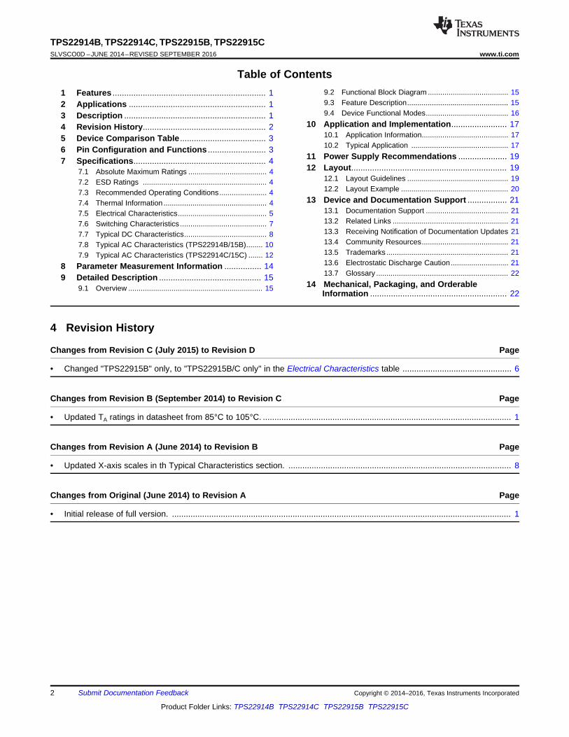
Table of Contents1 Features .................................................................. 12 Applications ........................................................... 13 Description ............................................................. 14 Revision History..................................................... 25 Device Comparison Table ..................................... 36 Pin Configuration and Functions ......................... 37 Specifications......................................................... 4
7.1 Absolute Maximum Ratings ...................................... 47.2 ESD Ratings ............................................................ 47.3 Recommended Operating Conditions....................... 47.4 Thermal Information .................................................. 47.5 Electrical Characteristics........................................... 57.6 Switching Characteristics .......................................... 77.7 Typical DC Characteristics........................................ 87.8 Typical AC Characteristics (TPS22914B/15B)........ 107.9 Typical AC Characteristics (TPS22914C/15C) ....... 12
8 Parameter Measurement Information ................ 149 Detailed Description ............................................ 15
9.1 Overview ................................................................. 15
9.2 Functional Block Diagram ....................................... 159.3 Feature Description................................................. 159.4 Device Functional Modes........................................ 16
10 Application and Implementation........................ 1710.1 Application Information.......................................... 1710.2 Typical Application ............................................... 17
11 Power Supply Recommendations ..................... 1912 Layout................................................................... 19
12.1 Layout Guidelines ................................................. 1912.2 Layout Example .................................................... 20
13 Device and Documentation Support ................. 2113.1 Documentation Support ........................................ 2113.2 Related Links ........................................................ 2113.3 Receiving Notification of Documentation Updates 2113.4 Community Resources.......................................... 2113.5 Trademarks ........................................................... 2113.6 Electrostatic Discharge Caution............................ 2113.7 Glossary ................................................................ 22
14 Mechanical, Packaging, and OrderableInformation ........................................................... 22
4 Revision History
Changes from Revision C (July 2015) to Revision D Page
• Changed "TPS22915B" only, to "TPS22915B/C only" in the Electrical Characteristics table ............................................... 6
Changes from Revision B (September 2014) to Revision C Page
• Updated TA ratings in datasheet from 85°C to 105°C. ........................................................................................................... 1
Changes from Revision A (June 2014) to Revision B Page
• Updated X-axis scales in th Typical Characteristics section. ................................................................................................ 8
Changes from Original (June 2014) to Revision A Page
• Initial release of full version. .................................................................................................................................................. 1
B
A
2 1
B
A
1 2BUMP VIEWLASER MARKING VIEW
3
TPS22914B, TPS22914C, TPS22915B, TPS22915Cwww.ti.com SLVSCO0D –JUNE 2014–REVISED SEPTEMBER 2016
Product Folder Links: TPS22914B TPS22914C TPS22915B TPS22915C
Submit Documentation FeedbackCopyright © 2014–2016, Texas Instruments Incorporated
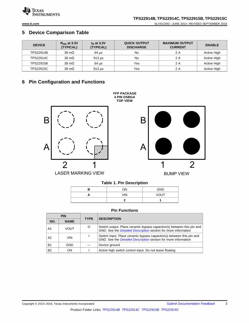
5 Device Comparison Table
DEVICE RON at 3.3V(TYPICAL)
tR at 3.3V(TYPICAL)
QUICK OUTPUTDISCHARGE
MAXIMUM OUTPUTCURRENT ENABLE
TPS22914B 38 mΩ 64 µs No 2 A Active HighTPS22914C 38 mΩ 913 µs No 2 A Active HighTPS22915B 38 mΩ 64 µs Yes 2 A Active HighTPS22915C 38 mΩ 913 µs Yes 2 A Active High
6 Pin Configuration and Functions
YFP PACKAGE4 PIN DSBGA
TOP VIEW
Table 1. Pin DescriptionB ON GNDA VIN VOUT
2 1
Pin FunctionsPIN
TYPE DESCRIPTIONNO. NAME
A1 VOUT O Switch output. Place ceramic bypass capacitor(s) between this pin andGND. See the Detailed Description section for more information
A2 VIN I Switch input. Place ceramic bypass capacitor(s) between this pin andGND. See the Detailed Description section for more information
B1 GND — Device groundB2 ON I Active high switch control input. Do not leave floating
4
TPS22914B, TPS22914C, TPS22915B, TPS22915CSLVSCO0D –JUNE 2014–REVISED SEPTEMBER 2016 www.ti.com
Product Folder Links: TPS22914B TPS22914C TPS22915B TPS22915C
Submit Documentation Feedback Copyright © 2014–2016, Texas Instruments Incorporated
(1) Stresses beyond those listed under Absolute Maximum Ratings may cause permanent damage to the device. These are stress ratingsonly, which do not imply functional operation of the device at these or any other conditions beyond those indicated under RecommendedOperating Conditions. Exposure to absolute-maximum-rated conditions for extended periods may affect device reliability.
(2) All voltage values are with respect to network ground terminal.
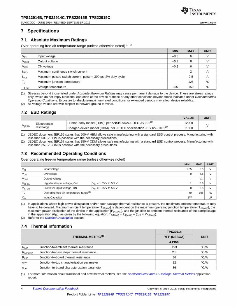
7 Specifications
7.1 Absolute Maximum RatingsOver operating free-air temperature range (unless otherwise noted) (1) (2)
MIN MAX UNITVIN Input voltage –0.3 6 VVOUT Output voltage –0.3 6 VVON ON voltage –0.3 6 VIMAX Maximum continuous switch current 2 AIPLS Maximum pulsed switch current, pulse < 300 µs, 2% duty cycle 2.5 ATJ Maximum junction temperature 125 °CTSTG Storage temperature –65 150 °C
(1) JEDEC document JEP155 states that 500-V HBM allows safe manufacturing with a standard ESD control process. Manufacturing withless than 500-V HBM is possible with the necessary precautions.
(2) JEDEC document JEP157 states that 250-V CDM allows safe manufacturing with a standard ESD control process. Manufacturing withless than 250-V CDM is possible with the necessary precautions.
7.2 ESD RatingsVALUE UNIT
V(ESD)Electrostaticdischarge
Human-body model (HBM), per ANSI/ESDA/JEDEC JS-001 (1) ±2000V
Charged-device model (CDM), per JEDEC specification JESD22-C101 (2) ±1000
(1) In applications where high power dissipation and/or poor package thermal resistance is present, the maximum ambient temperature mayhave to be derated. Maximum ambient temperature [TA(max)] is dependent on the maximum operating junction temperature [TJ(MAX)], themaximum power dissipation of the device in the application [PD(MAX)], and the junction-to-ambient thermal resistance of the part/packagein the application (θJA), as given by the following equation: TA(MAX) = TJ(MAX) – (θJA × PD(MAX)).
(2) Refer to the Detailed Description section.
7.3 Recommended Operating ConditionsOver operating free-air temperature range (unless otherwise noted)
MIN MAX UNIT
VIN Input voltage 1.05 5.5 V
VON ON voltage 0 5.5 V
VOUT Output voltage VIN V
VIH, ON High-level input voltage, ON VIN = 1.05 V to 5.5 V 1 5.5 V
VIL, ON Low-level input voltage, ON VIN = 1.05 V to 5.5 V 0 0.5 V
TA Operating free-air temperature range (1) –40 105 °C
CIN Input Capacitor 1 (2) µF
(1) For more information about traditional and new thermal metrics, see the Semiconductor and IC Package Thermal Metrics applicationreport.
7.4 Thermal Information
THERMAL METRIC (1)TPS2291x
UNITYFP (DSBGA)4 PINS
RθJA Junction-to-ambient thermal resistance 193 °C/WRθJC(top) Junction-to-case (top) thermal resistance 2.3 °C/WRθJB Junction-to-board thermal resistance 36 °C/WψJT Junction-to-top characterization parameter 12 °C/WψJB Junction-to-board characterization parameter 36 °C/W
5
TPS22914B, TPS22914C, TPS22915B, TPS22915Cwww.ti.com SLVSCO0D –JUNE 2014–REVISED SEPTEMBER 2016
Product Folder Links: TPS22914B TPS22914C TPS22915B TPS22915C
Submit Documentation FeedbackCopyright © 2014–2016, Texas Instruments Incorporated
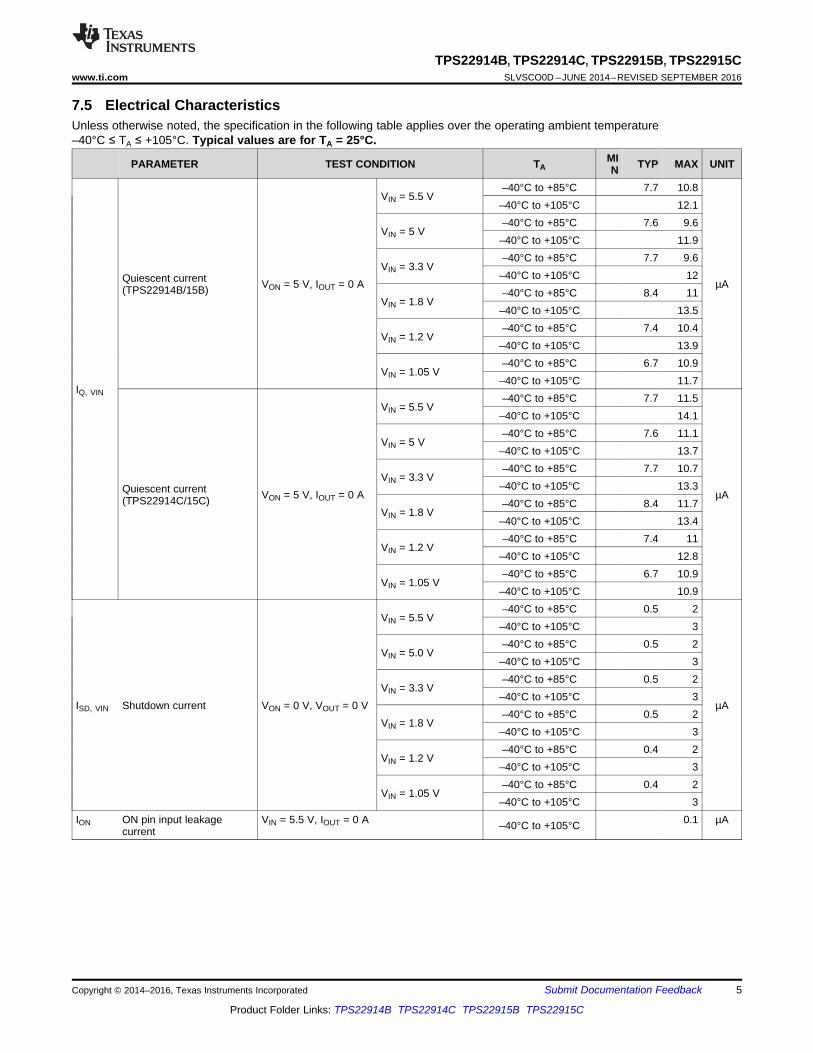
7.5 Electrical CharacteristicsUnless otherwise noted, the specification in the following table applies over the operating ambient temperature–40°C ≤ TA ≤ +105°C. Typical values are for TA = 25°C.
PARAMETER TEST CONDITION TAMIN TYP MAX UNIT
IQ, VIN
Quiescent current(TPS22914B/15B) VON = 5 V, IOUT = 0 A
VIN = 5.5 V–40°C to +85°C 7.7 10.8
µA
–40°C to +105°C 12.1
VIN = 5 V–40°C to +85°C 7.6 9.6–40°C to +105°C 11.9
VIN = 3.3 V–40°C to +85°C 7.7 9.6–40°C to +105°C 12
VIN = 1.8 V–40°C to +85°C 8.4 11–40°C to +105°C 13.5
VIN = 1.2 V–40°C to +85°C 7.4 10.4–40°C to +105°C 13.9
VIN = 1.05 V–40°C to +85°C 6.7 10.9–40°C to +105°C 11.7
Quiescent current(TPS22914C/15C) VON = 5 V, IOUT = 0 A
VIN = 5.5 V–40°C to +85°C 7.7 11.5
µA
–40°C to +105°C 14.1
VIN = 5 V–40°C to +85°C 7.6 11.1–40°C to +105°C 13.7
VIN = 3.3 V–40°C to +85°C 7.7 10.7–40°C to +105°C 13.3
VIN = 1.8 V–40°C to +85°C 8.4 11.7–40°C to +105°C 13.4
VIN = 1.2 V–40°C to +85°C 7.4 11–40°C to +105°C 12.8
VIN = 1.05 V–40°C to +85°C 6.7 10.9–40°C to +105°C 10.9
ISD, VIN Shutdown current VON = 0 V, VOUT = 0 V
VIN = 5.5 V–40°C to +85°C 0.5 2
µA
–40°C to +105°C 3
VIN = 5.0 V–40°C to +85°C 0.5 2–40°C to +105°C 3
VIN = 3.3 V–40°C to +85°C 0.5 2–40°C to +105°C 3
VIN = 1.8 V–40°C to +85°C 0.5 2–40°C to +105°C 3
VIN = 1.2 V–40°C to +85°C 0.4 2–40°C to +105°C 3
VIN = 1.05 V–40°C to +85°C 0.4 2–40°C to +105°C 3
ION ON pin input leakagecurrent
VIN = 5.5 V, IOUT = 0 A –40°C to +105°C 0.1 µA
6
TPS22914B, TPS22914C, TPS22915B, TPS22915CSLVSCO0D –JUNE 2014–REVISED SEPTEMBER 2016 www.ti.com
Product Folder Links: TPS22914B TPS22914C TPS22915B TPS22915C
Submit Documentation Feedback Copyright © 2014–2016, Texas Instruments Incorporated
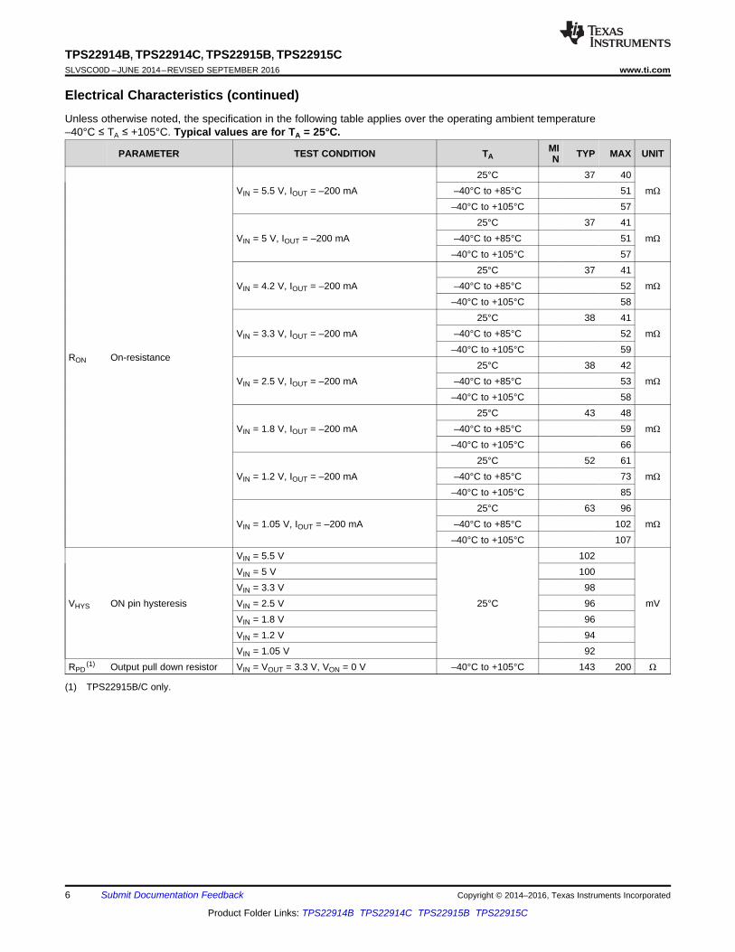
Electrical Characteristics (continued)Unless otherwise noted, the specification in the following table applies over the operating ambient temperature–40°C ≤ TA ≤ +105°C. Typical values are for TA = 25°C.
PARAMETER TEST CONDITION TAMIN TYP MAX UNIT
(1) TPS22915B/C only.
RON On-resistance
VIN = 5.5 V, IOUT = –200 mA25°C 37 40
mΩ–40°C to +85°C 51–40°C to +105°C 57
VIN = 5 V, IOUT = –200 mA25°C 37 41
mΩ–40°C to +85°C 51–40°C to +105°C 57
VIN = 4.2 V, IOUT = –200 mA25°C 37 41
mΩ–40°C to +85°C 52–40°C to +105°C 58
VIN = 3.3 V, IOUT = –200 mA25°C 38 41
mΩ–40°C to +85°C 52–40°C to +105°C 59
VIN = 2.5 V, IOUT = –200 mA25°C 38 42
mΩ–40°C to +85°C 53–40°C to +105°C 58
VIN = 1.8 V, IOUT = –200 mA25°C 43 48
mΩ–40°C to +85°C 59–40°C to +105°C 66
VIN = 1.2 V, IOUT = –200 mA25°C 52 61
mΩ–40°C to +85°C 73–40°C to +105°C 85
VIN = 1.05 V, IOUT = –200 mA25°C 63 96
mΩ–40°C to +85°C 102–40°C to +105°C 107
VHYS ON pin hysteresis
VIN = 5.5 V
25°C
102
mV
VIN = 5 V 100VIN = 3.3 V 98VIN = 2.5 V 96VIN = 1.8 V 96VIN = 1.2 V 94VIN = 1.05 V 92
RPD(1) Output pull down resistor VIN = VOUT = 3.3 V, VON = 0 V –40°C to +105°C 143 200 Ω
7
TPS22914B, TPS22914C, TPS22915B, TPS22915Cwww.ti.com SLVSCO0D –JUNE 2014–REVISED SEPTEMBER 2016
Product Folder Links: TPS22914B TPS22914C TPS22915B TPS22915C
Submit Documentation FeedbackCopyright © 2014–2016, Texas Instruments Incorporated
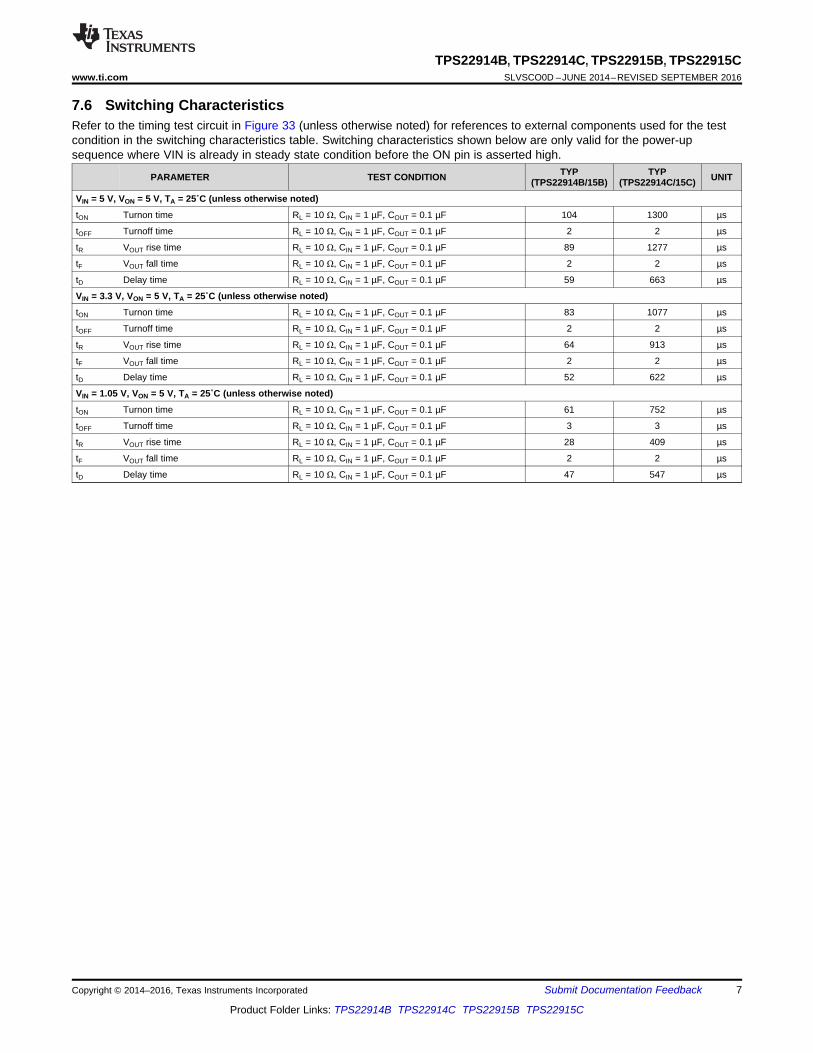
7.6 Switching CharacteristicsRefer to the timing test circuit in Figure 33 (unless otherwise noted) for references to external components used for the testcondition in the switching characteristics table. Switching characteristics shown below are only valid for the power-upsequence where VIN is already in steady state condition before the ON pin is asserted high.
PARAMETER TEST CONDITION TYP(TPS22914B/15B)
TYP(TPS22914C/15C) UNIT
VIN = 5 V, VON = 5 V, TA = 25˚C (unless otherwise noted)
tON Turnon time RL = 10 Ω, CIN = 1 µF, COUT = 0.1 µF 104 1300 µs
tOFF Turnoff time RL = 10 Ω, CIN = 1 µF, COUT = 0.1 µF 2 2 µs
tR VOUT rise time RL = 10 Ω, CIN = 1 µF, COUT = 0.1 µF 89 1277 µs
tF VOUT fall time RL = 10 Ω, CIN = 1 µF, COUT = 0.1 µF 2 2 µs
tD Delay time RL = 10 Ω, CIN = 1 µF, COUT = 0.1 µF 59 663 µs
VIN = 3.3 V, VON = 5 V, TA = 25˚C (unless otherwise noted)
tON Turnon time RL = 10 Ω, CIN = 1 µF, COUT = 0.1 µF 83 1077 µs
tOFF Turnoff time RL = 10 Ω, CIN = 1 µF, COUT = 0.1 µF 2 2 µs
tR VOUT rise time RL = 10 Ω, CIN = 1 µF, COUT = 0.1 µF 64 913 µs
tF VOUT fall time RL = 10 Ω, CIN = 1 µF, COUT = 0.1 µF 2 2 µs
tD Delay time RL = 10 Ω, CIN = 1 µF, COUT = 0.1 µF 52 622 µs
VIN = 1.05 V, VON = 5 V, TA = 25˚C (unless otherwise noted)
tON Turnon time RL = 10 Ω, CIN = 1 µF, COUT = 0.1 µF 61 752 µs
tOFF Turnoff time RL = 10 Ω, CIN = 1 µF, COUT = 0.1 µF 3 3 µs
tR VOUT rise time RL = 10 Ω, CIN = 1 µF, COUT = 0.1 µF 28 409 µs
tF VOUT fall time RL = 10 Ω, CIN = 1 µF, COUT = 0.1 µF 2 2 µs
tD Delay time RL = 10 Ω, CIN = 1 µF, COUT = 0.1 µF 47 547 µs
VIN (V)
RO
N (
m:
)
1.05 1.55 2.05 2.55 3.05 3.55 4.05 4.55 5.05 5.520
30
40
50
60
70
80
D005
-40°C 25°C 85°C105°C
IOUT (A)
RO
N (
m:
)
0 0.5 1 1.5 20
10
20
30
40
50
60
70
80
D006
VIN = 1.05VVIN = 1.2VVIN = 1.5V
VIN = 1.8VVIN = 2.5VVIN = 3.3V
VIN = 4.2VVIN = 5VVIN = 5.5V
VIN (V)
I SD (P
A)
1.05 1.55 2.05 2.55 3.05 3.55 4.05 4.55 5.05 5.50
0.4
0.8
1.2
1.6
2
2.4
2.8
D003
-40°C25°C 85°C 105°C
Junction Temperature (qC)
RO
N (
m:
)
-40 -25 -10 5 20 35 50 65 80 95 110 1250
10
20
30
40
50
60
70
80
D004
VIN = 1.05VVIN = 1.2VVIN = 1.5V
VIN = 1.8VVIN = 2.5VVIN = 3.3V
VIN = 4.2VVIN = 5VVIN = 5.5V
VIN (V)
I Q (P
A)
1.05 1.55 2.05 2.55 3.05 3.55 4.05 4.55 5.05 5.53
4
5
6
7
8
9
10
11
D001
-40°C 25°C 85°C 105°C
VIN (V)
I Q (P
A)
1.05 1.55 2.05 2.55 3.05 3.55 4.05 4.55 5.05 5.53
4
5
6
7
8
9
10
11
D002
-40°C25°C85°C105°C
8
TPS22914B, TPS22914C, TPS22915B, TPS22915CSLVSCO0D –JUNE 2014–REVISED SEPTEMBER 2016 www.ti.com
Product Folder Links: TPS22914B TPS22914C TPS22915B TPS22915C
Submit Documentation Feedback Copyright © 2014–2016, Texas Instruments Incorporated
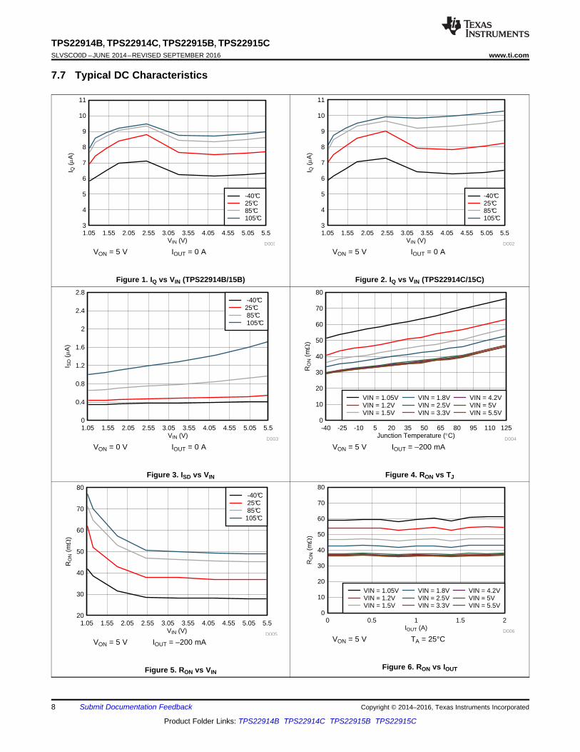
7.7 Typical DC Characteristics
VON = 5 V IOUT = 0 A
Figure 1. IQ vs VIN (TPS22914B/15B)
VON = 5 V IOUT = 0 A
Figure 2. IQ vs VIN (TPS22914C/15C)
VON = 0 V IOUT = 0 A
Figure 3. ISD vs VIN
VON = 5 V IOUT = –200 mA
Figure 4. RON vs TJ
VON = 5 V IOUT = –200 mA
Figure 5. RON vs VIN
VON = 5 V TA = 25°C
Figure 6. RON vs IOUT
VIN (V)
VH
YS (
V)
1.05 1.55 2.05 2.55 3.05 3.55 4.05 4.55 5.05 5.570
80
90
100
110
120
130
140
150
160
170
D009
-40°C25°C85°C105°C
VIN (V)
RP
D (:
)
1.05 1.55 2.05 2.55 3.05 3.55 4.05 4.55 5.05 5.5140
145
150
155
160
165
170
175
180
185
190
D010
-40°C 25°C 85°C105°C
VIN (V)
VIL
(V
)
1.05 1.55 2.05 2.55 3.05 3.55 4.05 4.55 5.05 5.50.5
0.55
0.6
0.65
0.7
0.75
0.8
0.85
0.9
0.95
1
D007
-40°C25°C85°C105°C
VIN (V)
VIH
(V
)
1.05 1.55 2.05 2.55 3.05 3.55 4.05 4.55 5.05 5.50.5
0.55
0.6
0.65
0.7
0.75
0.8
0.85
0.9
0.95
1
D008
-40°C25°C85°C105°C
9
TPS22914B, TPS22914C, TPS22915B, TPS22915Cwww.ti.com SLVSCO0D –JUNE 2014–REVISED SEPTEMBER 2016
Product Folder Links: TPS22914B TPS22914C TPS22915B TPS22915C
Submit Documentation FeedbackCopyright © 2014–2016, Texas Instruments Incorporated
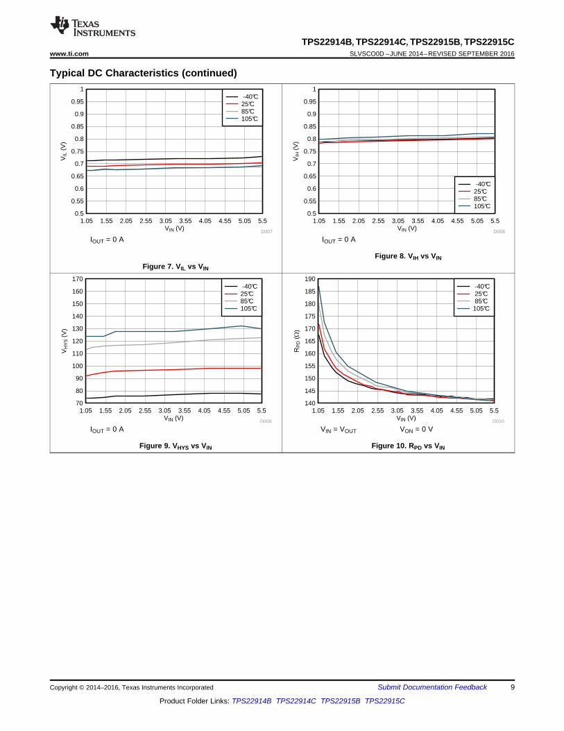
Typical DC Characteristics (continued)
IOUT = 0 A
Figure 7. VIL vs VIN
IOUT = 0 A
Figure 8. VIH vs VIN
IOUT = 0 A
Figure 9. VHYS vs VIN
VIN = VOUT VON = 0 V
Figure 10. RPD vs VIN
VIN (V)
t ON (P
s)
1.05 1.55 2.05 2.55 3.05 3.55 4.05 4.55 5.05 5.550
60
70
80
90
100
110
120
D015
-40°C25°C85°C105°C
VIN (V)
t OF
F (P
s)
1.05 1.55 2.05 2.55 3.05 3.55 4.05 4.55 5.05 5.50
0.5
1
1.5
2
2.5
3
3.5
4
4.5
5
D014
-40°C25°C85°C105°C
VIN (V)
t F (P
s)
1.05 1.55 2.05 2.55 3.05 3.55 4.05 4.55 5.05 5.50
0.5
1
1.5
2
2.5
3
3.5
4
4.5
5
D013
-40°C25°C85°C105°C
VIN (V)
t R (P
s)
1.05 1.55 2.05 2.55 3.05 3.55 4.05 4.55 5.05 5.520
30
40
50
60
70
80
90
100
D011
-40°C25°C85°C105°C
VIN (V)
t D (P
s)
1.05 1.55 2.05 2.55 3.05 3.55 4.05 4.55 5.05 5.535
40
45
50
55
60
65
70
D012
-40°C25°C85°C105°C
10
TPS22914B, TPS22914C, TPS22915B, TPS22915CSLVSCO0D –JUNE 2014–REVISED SEPTEMBER 2016 www.ti.com
Product Folder Links: TPS22914B TPS22914C TPS22915B TPS22915C
Submit Documentation Feedback Copyright © 2014–2016, Texas Instruments Incorporated
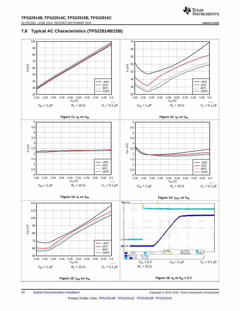
7.8 Typical AC Characteristics (TPS22914B/15B)
CIN = 1 µF RL = 10 Ω CL = 0.1 µF
Figure 11. tR vs VIN
CIN = 1 µF RL = 10 Ω CL = 0.1 µF
Figure 12. tD vs VIN
CIN = 1 µF RL = 10 Ω CL = 0.1 µF
Figure 13. tF vs VIN
CIN = 1 µF RL = 10 Ω CL = 0.1 µF
Figure 14. tOFF vs VIN
CIN = 1 µF RL = 10 Ω CL = 0.1 µF
Figure 15. tON vs VIN
VIN = 5 V CIN = 1 µF CL = 0.1 µFRL = 10 Ω
Figure 16. tR at VIN = 5 V
11
TPS22914B, TPS22914C, TPS22915B, TPS22915Cwww.ti.com SLVSCO0D –JUNE 2014–REVISED SEPTEMBER 2016
Product Folder Links: TPS22914B TPS22914C TPS22915B TPS22915C
Submit Documentation FeedbackCopyright © 2014–2016, Texas Instruments Incorporated
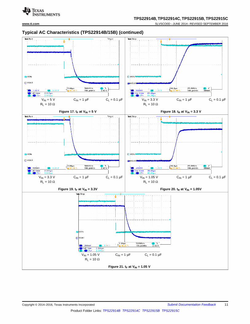
Typical AC Characteristics (TPS22914B/15B) (continued)
VIN = 5 V CIN = 1 µF CL = 0.1 µFRL = 10 Ω
Figure 17. tF at VIN = 5 V
VIN = 3.3 V CIN = 1 µF CL = 0.1 µFRL = 10 Ω
Figure 18. tR at VIN = 3.3 V
VIN = 3.3 V CIN = 1 µF CL = 0.1 µFRL = 10 Ω
Figure 19. tF at VIN = 3.3V
VIN = 1.05 V CIN = 1 µF CL = 0.1 µFRL = 10 Ω
Figure 20. tR at VIN = 1.05V
VIN = 1.05 V CIN = 1 µF CL = 0.1 µFRL = 10 Ω
Figure 21. tF at VIN = 1.05 V
VIN (V)
t ON (P
s)
1.05 1.55 2.05 2.55 3.05 3.55 4.05 4.55 5.05 5.5600
800
1000
1200
1400
1600
D020
-40°C25°C85°C105°C
VIN (V)
t F (P
s)
1.05 1.55 2.05 2.55 3.05 3.55 4.05 4.55 5.05 5.50
0.5
1
1.5
2
2.5
3
3.5
4
4.5
5
D018
-40°C25°C85°C105°C
VIN (V)
t OF
F (P
s)
1.05 1.55 2.05 2.55 3.05 3.55 4.05 4.55 5.05 5.50
0.5
1
1.5
2
2.5
3
3.5
4
4.5
5
D019
-40°C25°C85°C105°C
VIN (V)
t R (P
s)
1.05 1.55 2.05 2.55 3.05 3.55 4.05 4.55 5.05 5.5300
500
700
900
1100
1300
1500
D016
-40°C25°C85°C105°C
VIN (V)
t D (P
s)
1.05 1.55 2.05 2.55 3.05 3.55 4.05 4.55 5.05 5.5450
500
550
600
650
700
750
D017
-40°C25°C85°C105°C
12
TPS22914B, TPS22914C, TPS22915B, TPS22915CSLVSCO0D –JUNE 2014–REVISED SEPTEMBER 2016 www.ti.com
Product Folder Links: TPS22914B TPS22914C TPS22915B TPS22915C
Submit Documentation Feedback Copyright © 2014–2016, Texas Instruments Incorporated
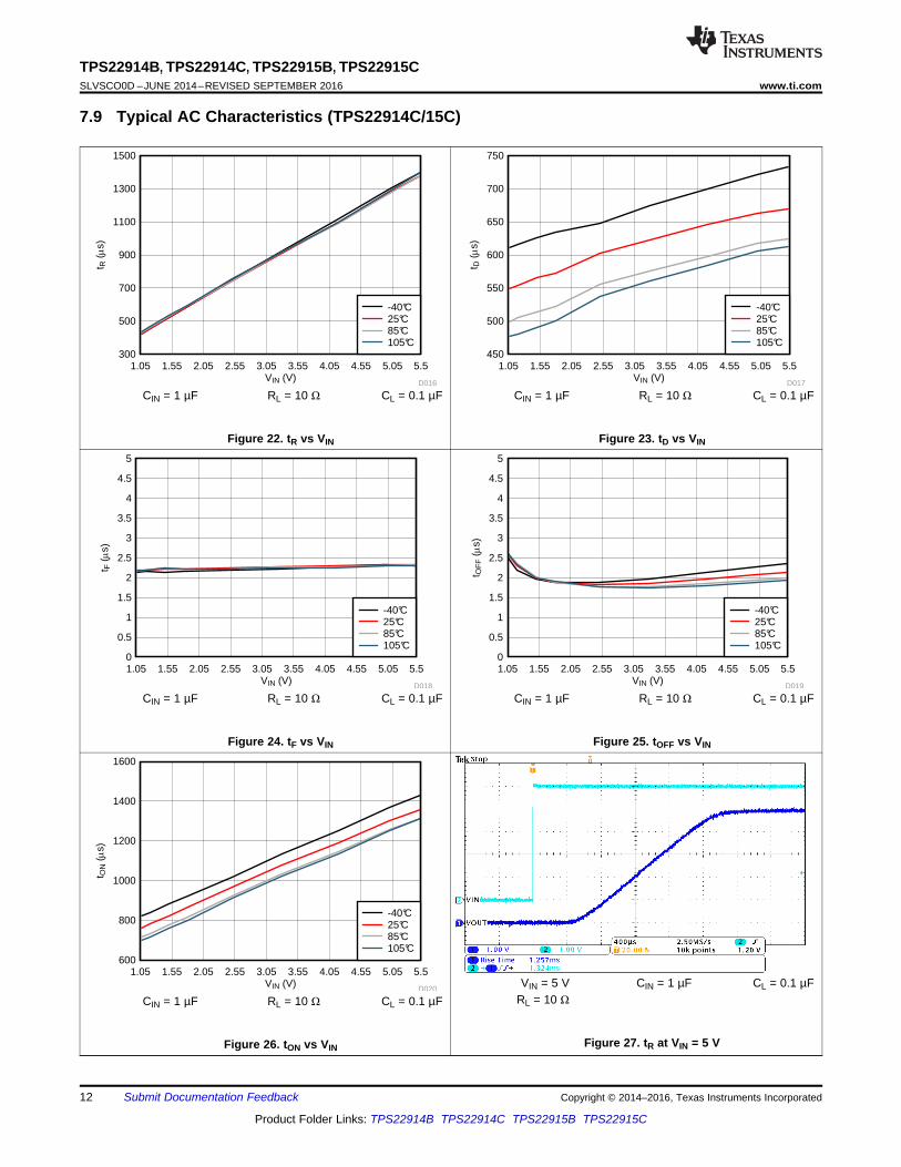
7.9 Typical AC Characteristics (TPS22914C/15C)
CIN = 1 µF RL = 10 Ω CL = 0.1 µF
Figure 22. tR vs VIN
CIN = 1 µF RL = 10 Ω CL = 0.1 µF
Figure 23. tD vs VIN
CIN = 1 µF RL = 10 Ω CL = 0.1 µF
Figure 24. tF vs VIN
CIN = 1 µF RL = 10 Ω CL = 0.1 µF
Figure 25. tOFF vs VIN
CIN = 1 µF RL = 10 Ω CL = 0.1 µF
Figure 26. tON vs VIN
VIN = 5 V CIN = 1 µF CL = 0.1 µFRL = 10 Ω
Figure 27. tR at VIN = 5 V
13
TPS22914B, TPS22914C, TPS22915B, TPS22915Cwww.ti.com SLVSCO0D –JUNE 2014–REVISED SEPTEMBER 2016
Product Folder Links: TPS22914B TPS22914C TPS22915B TPS22915C
Submit Documentation FeedbackCopyright © 2014–2016, Texas Instruments Incorporated
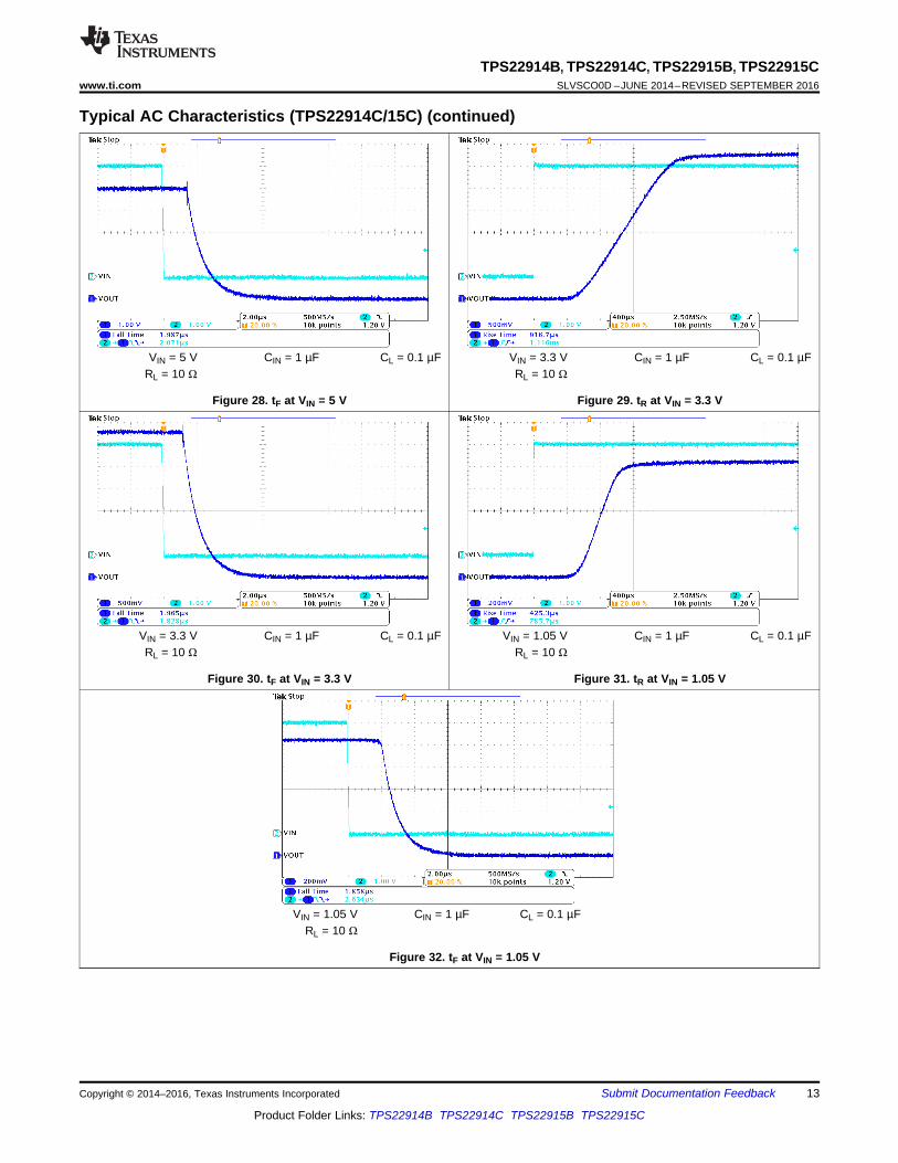
Typical AC Characteristics (TPS22914C/15C) (continued)
VIN = 5 V CIN = 1 µF CL = 0.1 µFRL = 10 Ω
Figure 28. tF at VIN = 5 V
VIN = 3.3 V CIN = 1 µF CL = 0.1 µFRL = 10 Ω
Figure 29. tR at VIN = 3.3 V
VIN = 3.3 V CIN = 1 µF CL = 0.1 µFRL = 10 Ω
Figure 30. tF at VIN = 3.3 V
VIN = 1.05 V CIN = 1 µF CL = 0.1 µFRL = 10 Ω
Figure 31. tR at VIN = 1.05 V
VIN = 1.05 V CIN = 1 µF CL = 0.1 µFRL = 10 Ω
Figure 32. tF at VIN = 1.05 V
tRtON
tOFF
90% 90%
10% 10%
VON
VOUT
VOUT
50% 50%
50% 50%
tD
10%
tF
RL
+
-
OFF
ON
TPS22914/15
VIN VOUT
CL
GND
(A)
GND
ON GND
CIN = 1 µF
14
TPS22914B, TPS22914C, TPS22915B, TPS22915CSLVSCO0D –JUNE 2014–REVISED SEPTEMBER 2016 www.ti.com
Product Folder Links: TPS22914B TPS22914C TPS22915B TPS22915C
Submit Documentation Feedback Copyright © 2014–2016, Texas Instruments Incorporated
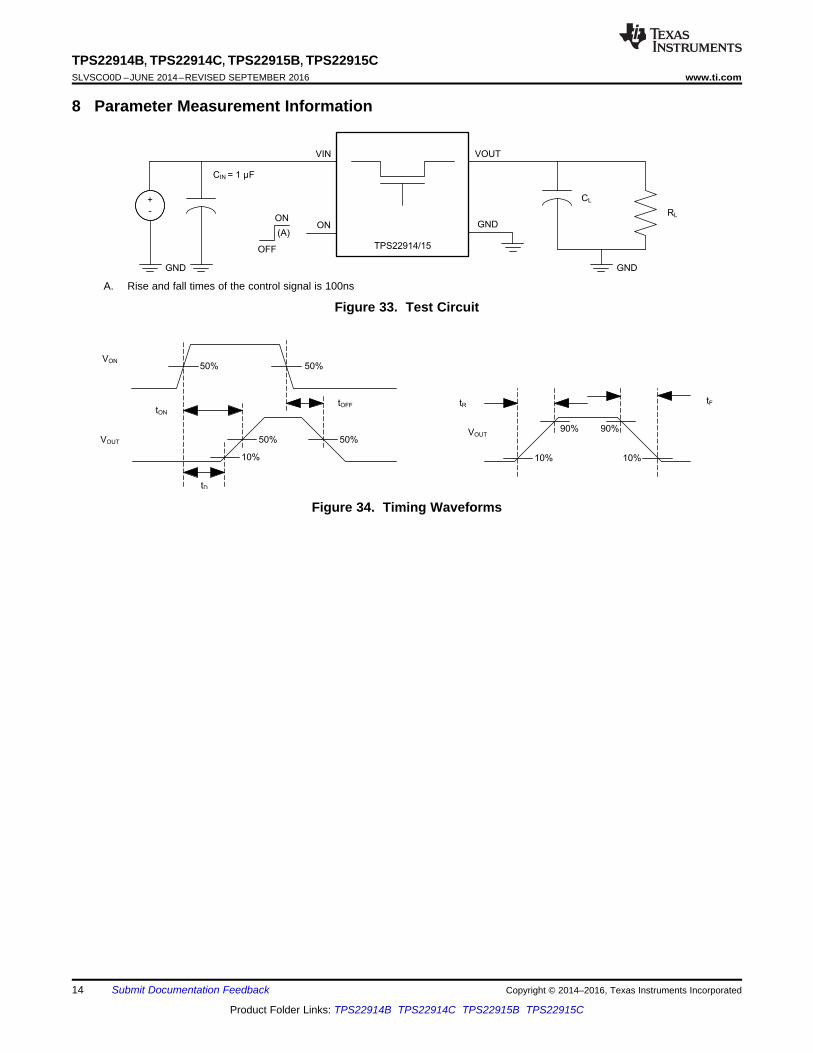
8 Parameter Measurement Information
A. Rise and fall times of the control signal is 100ns
Figure 33. Test Circuit
Figure 34. Timing Waveforms
Control Logic
VIN
ON
VOUT
GND
Driver
TPS22915 Only
ChargePump
15
TPS22914B, TPS22914C, TPS22915B, TPS22915Cwww.ti.com SLVSCO0D –JUNE 2014–REVISED SEPTEMBER 2016
Product Folder Links: TPS22914B TPS22914C TPS22915B TPS22915C
Submit Documentation FeedbackCopyright © 2014–2016, Texas Instruments Incorporated
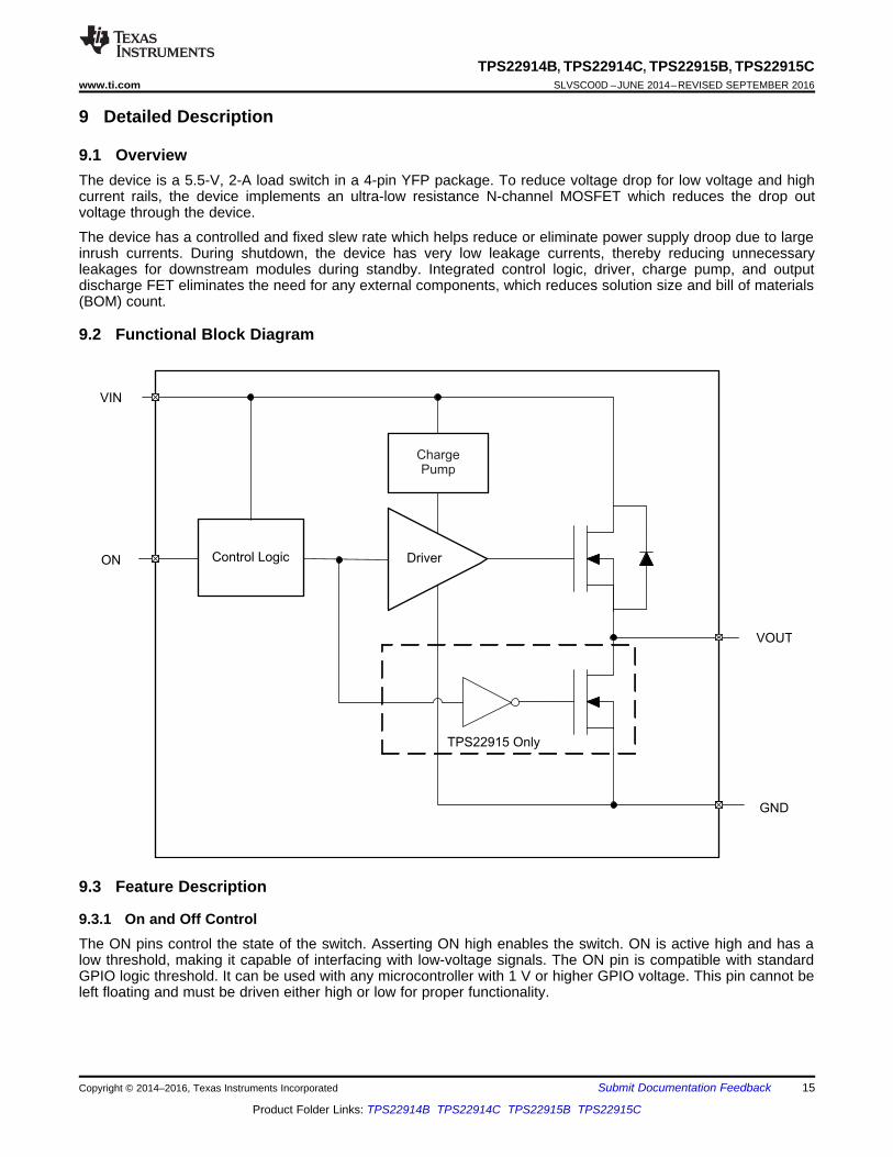
9 Detailed Description
9.1 OverviewThe device is a 5.5-V, 2-A load switch in a 4-pin YFP package. To reduce voltage drop for low voltage and highcurrent rails, the device implements an ultra-low resistance N-channel MOSFET which reduces the drop outvoltage through the device.
The device has a controlled and fixed slew rate which helps reduce or eliminate power supply droop due to largeinrush currents. During shutdown, the device has very low leakage currents, thereby reducing unnecessaryleakages for downstream modules during standby. Integrated control logic, driver, charge pump, and outputdischarge FET eliminates the need for any external components, which reduces solution size and bill of materials(BOM) count.
9.2 Functional Block Diagram
9.3 Feature Description
9.3.1 On and Off ControlThe ON pins control the state of the switch. Asserting ON high enables the switch. ON is active high and has alow threshold, making it capable of interfacing with low-voltage signals. The ON pin is compatible with standardGPIO logic threshold. It can be used with any microcontroller with 1 V or higher GPIO voltage. This pin cannot beleft floating and must be driven either high or low for proper functionality.
16
TPS22914B, TPS22914C, TPS22915B, TPS22915CSLVSCO0D –JUNE 2014–REVISED SEPTEMBER 2016 www.ti.com
Product Folder Links: TPS22914B TPS22914C TPS22915B TPS22915C
Submit Documentation Feedback Copyright © 2014–2016, Texas Instruments Incorporated
Feature Description (continued)9.3.2 Input Capacitor (CIN)To limit the voltage drop on the input supply caused by transient in-rush currents when the switch turns on into adischarged load capacitor or short-circuit, a capacitor needs to be placed between VIN and GND. A 1-µF ceramiccapacitor, CIN, placed close to the pins, is usually sufficient. Higher values of CIN can be used to further reducethe voltage drop during high-current application. When switching heavy loads, it is recommended to have aninput capacitor about 10 times higher than the output capacitor to avoid excessive voltage drop.
9.3.3 Output Capacitor (CL)Due to the integrated body diode in the MOSFET, a CIN greater than CL is highly recommended. A CL greaterthan CIN can cause VOUT to exceed VIN when the system supply is removed. This could result in current flowthrough the body diode from VOUT to VIN. A CIN to CL ratio of 10 to 1 is recommended for minimizing VIN dipcaused by inrush currents during startup.
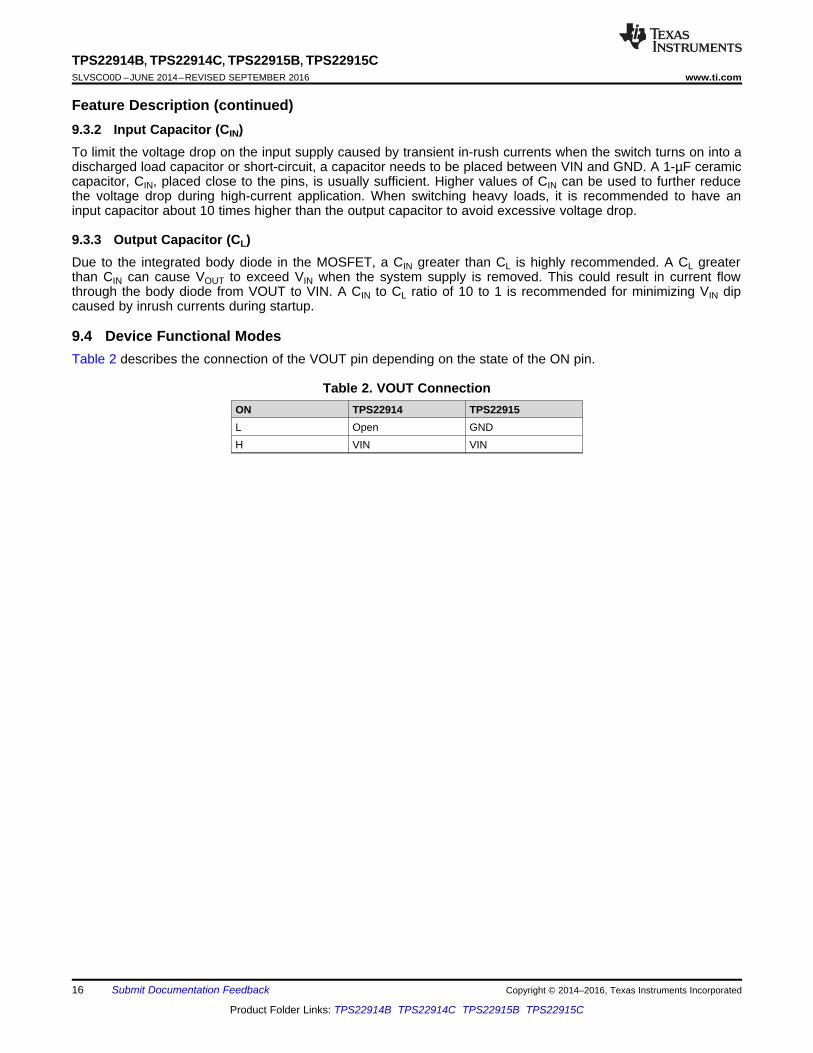
9.4 Device Functional ModesTable 2 describes the connection of the VOUT pin depending on the state of the ON pin.
Table 2. VOUT ConnectionON TPS22914 TPS22915L Open GNDH VIN VIN
VIN
TPS22914/15
VIN VOUT
ON GNDON
VOUT
CIN CL
17
TPS22914B, TPS22914C, TPS22915B, TPS22915Cwww.ti.com SLVSCO0D –JUNE 2014–REVISED SEPTEMBER 2016
Product Folder Links: TPS22914B TPS22914C TPS22915B TPS22915C
Submit Documentation FeedbackCopyright © 2014–2016, Texas Instruments Incorporated
10 Application and Implementation
NOTEInformation in the following applications sections is not part of the TI componentspecification, and TI does not warrant its accuracy or completeness. TI’s customers areresponsible for determining suitability of components for their purposes. Customers shouldvalidate and test their design implementation to confirm system functionality.
10.1 Application InformationThis section highlights some of the design considerations when implementing this device in various applications.A PSPICE model for this device is also available in the product page of this device.
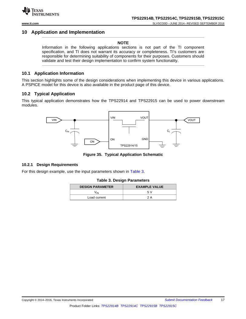
10.2 Typical ApplicationThis typical application demonstrates how the TPS22914 and TPS22915 can be used to power downstreammodules.
Figure 35. Typical Application Schematic
10.2.1 Design RequirementsFor this design example, use the input parameters shown in Table 3.
Table 3. Design ParametersDESIGN PARAMETER EXAMPLE VALUE
VIN 5 VLoad current 2 A
OUTINRUSH L
dVI C
dt= ´
18
TPS22914B, TPS22914C, TPS22915B, TPS22915CSLVSCO0D –JUNE 2014–REVISED SEPTEMBER 2016 www.ti.com
Product Folder Links: TPS22914B TPS22914C TPS22915B TPS22915C
Submit Documentation Feedback Copyright © 2014–2016, Texas Instruments Incorporated
10.2.2 Detailed Design ProcedureTo begin the design process, the designer needs to know the following:• VIN voltage• Load Current
10.2.2.1 VIN to VOUT Voltage DropThe VIN to VOUT voltage drop in the device is determined by the RON of the device and the load current. TheRON of the device depends upon the VIN conditions of the device. Refer to the RON specification of the device inthe Electrical Characteristics table of this datasheet. Once the RON of the device is determined based upon theVIN conditions, use Equation 1 to calculate the VIN to VOUT voltage drop.
∆V = ILOAD × RON
where• ΔV = voltage drop from VIN to VOUT• ILOAD = load current• RON = On-resistance of the device for a specific VIN (1)
An appropriate ILOAD must be chosen such that the IMAX specification of the device is not violated.
10.2.2.2 Inrush CurrentTo determine how much inrush current is caused by the CL capacitor, use Equation 2.
where• IINRUSH = amount of inrush caused by CL
• CL = capacitance on VOUT• dt = rise time in VOUT during the ramp up of VOUT when the device is enabled• dVOUT = change in VOUT during the ramp up of VOUT when the device is enabled (2)
An appropriate CL value must be placed on VOUT such that the IMAX and IPLS specifications of the device are notviolated.
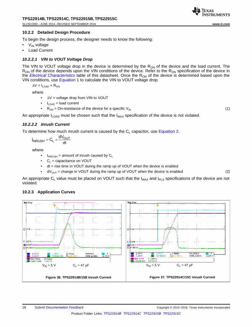
10.2.3 Application Curves
VIN = 5 V CL = 47 µF
Figure 36. TPS22914B/15B Inrush Current
VIN = 5 V CL = 47 µF
Figure 37. TPS22914C/15C Inrush Current
J(MAX) AD(MAX)
JA
T TP
-=
q
19
TPS22914B, TPS22914C, TPS22915B, TPS22915Cwww.ti.com SLVSCO0D –JUNE 2014–REVISED SEPTEMBER 2016
Product Folder Links: TPS22914B TPS22914C TPS22915B TPS22915C
Submit Documentation FeedbackCopyright © 2014–2016, Texas Instruments Incorporated
11 Power Supply RecommendationsThe device is designed to operate from a VIN range of 1.05 V to 5.5 V. This supply must be well regulated andplaced as close to the device terminal as possible with the recommended 1-µF bypass capacitor. If the supply islocated more than a few inches from the device terminals, additional bulk capacitance may be required inaddition to the ceramic bypass capacitors. If additional bulk capacitance is required, an electrolytic, tantalum, orceramic capacitor of 1 µF may be sufficient.
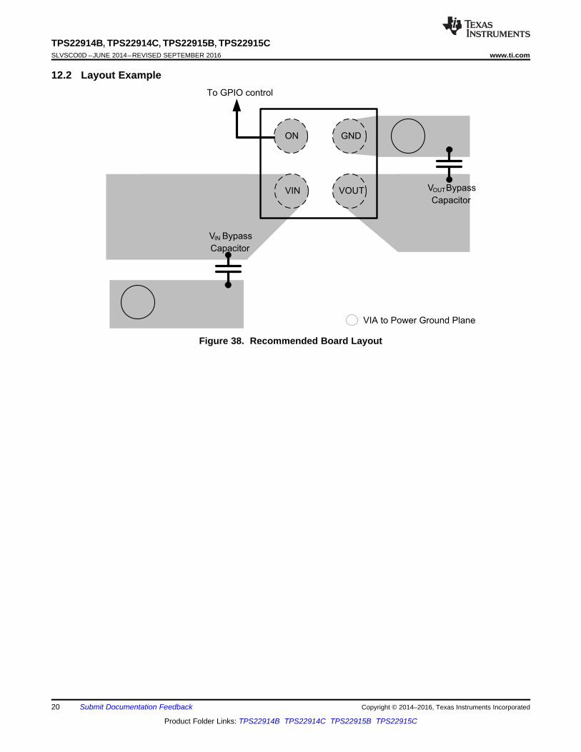
12 Layout
12.1 Layout Guidelines1. VIN and VOUT traces must be as short and wide as possible to accommodate for high current.2. The VIN pin must be bypassed to ground with low ESR ceramic bypass capacitors. The typical
recommended bypass capacitance is 1-μF ceramic with X5R or X7R dielectric. This capacitor must beplaced as close to the device pins as possible.
3. The VOUT pin must be bypassed to ground with low ESR ceramic bypass capacitors. The typicalrecommended bypass capacitance is one-tenth of the VIN bypass capacitor of X5R or X7R dielectric rating.This capacitor must be placed as close to the device pins as possible.
12.1.1 Thermal ConsiderationsFor best performance, all traces must be as short as possible. To be most effective, the input and outputcapacitors must be placed close to the device to minimize the effects that parasitic trace inductances may haveon normal and short-circuit operation. Using wide traces for VIN, VOUT, and GND helps minimize the parasiticelectrical effects along with minimizing the case to ambient thermal impedance.
The maximum IC junction temperature must be restricted to 125°C under normal operating conditions. Tocalculate the maximum allowable dissipation, PD(max) for a given output current and ambient temperature, useEquation 3.
where• PD(MAX) = maximum allowable power dissipation• TJ(MAX) = maximum allowable junction temperature (125°C for the TPS22914/15)• TA = ambient temperature of the device• θJA = junction to air thermal impedance. Refer to the Thermal Information table. This parameter is highly
dependent upon board layout. (3)
ON GND
VOUT
To GPIO control
VIA to Power Ground Plane
VIN Bypass
Capacitor
VOUTBypass
CapacitorVIN
20
TPS22914B, TPS22914C, TPS22915B, TPS22915CSLVSCO0D –JUNE 2014–REVISED SEPTEMBER 2016 www.ti.com
Product Folder Links: TPS22914B TPS22914C TPS22915B TPS22915C
Submit Documentation Feedback Copyright © 2014–2016, Texas Instruments Incorporated
12.2 Layout Example
Figure 38. Recommended Board Layout
21
TPS22914B, TPS22914C, TPS22915B, TPS22915Cwww.ti.com SLVSCO0D –JUNE 2014–REVISED SEPTEMBER 2016
Product Folder Links: TPS22914B TPS22914C TPS22915B TPS22915C
Submit Documentation FeedbackCopyright © 2014–2016, Texas Instruments Incorporated
13 Device and Documentation Support
13.1 Documentation Support
13.1.1 Related DocumentationFor related documentation see the following:• Basics of Load Switches• Managing Inrush Current• Load Switch Thermal Considerations• Using the TPS22915BEVM-078 Single Channel Load Switch IC• Implementing Ship Mode Using the TPS22915B Load Switches
13.2 Related LinksThe table below lists quick access links. Categories include technical documents, support and communityresources, tools and software, and quick access to sample or buy.
Table 4. Related Links
PARTS PRODUCT FOLDER SAMPLE & BUY TECHNICALDOCUMENTS
TOOLS &SOFTWARE
SUPPORT &COMMUNITY
TPS22914B Click here Click here Click here Click here Click hereTPS22914C Click here Click here Click here Click here Click hereTPS22915B Click here Click here Click here Click here Click hereTPS22915C Click here Click here Click here Click here Click here
13.3 Receiving Notification of Documentation UpdatesTo receive notification of documentation updates, navigate to the device product folder on ti.com. In the upperright corner, click on Alert me to register and receive a weekly digest of any product information that haschanged. For change details, review the revision history included in any revised document.
13.4 Community ResourcesThe following links connect to TI community resources. Linked contents are provided "AS IS" by the respectivecontributors. They do not constitute TI specifications and do not necessarily reflect TI's views; see TI's Terms ofUse.
TI E2E™ Online Community TI's Engineer-to-Engineer (E2E) Community. Created to foster collaborationamong engineers. At e2e.ti.com, you can ask questions, share knowledge, explore ideas and helpsolve problems with fellow engineers.
Design Support TI's Design Support Quickly find helpful E2E forums along with design support tools andcontact information for technical support.
13.5 TrademarksE2E is a trademark of Texas Instruments.Ultrabook is a trademark of Intel.All other trademarks are the property of their respective owners.
13.6 Electrostatic Discharge CautionThis integrated circuit can be damaged by ESD. Texas Instruments recommends that all integrated circuits be handled withappropriate precautions. Failure to observe proper handling and installation procedures can cause damage.
ESD damage can range from subtle performance degradation to complete device failure. Precision integrated circuits may be moresusceptible to damage because very small parametric changes could cause the device not to meet its published specifications.
22
TPS22914B, TPS22914C, TPS22915B, TPS22915CSLVSCO0D –JUNE 2014–REVISED SEPTEMBER 2016 www.ti.com
Product Folder Links: TPS22914B TPS22914C TPS22915B TPS22915C
Submit Documentation Feedback Copyright © 2014–2016, Texas Instruments Incorporated
13.7 GlossarySLYZ022 — TI Glossary.
This glossary lists and explains terms, acronyms, and definitions.
14 Mechanical, Packaging, and Orderable InformationThe following pages include mechanical, packaging, and orderable information. This information is the mostcurrent data available for the designated devices. This data is subject to change without notice and revision ofthis document. For browser-based versions of this data sheet, refer to the left-hand navigation.
PACKAGE OPTION ADDENDUM
www.ti.com 23-Apr-2018
Addendum-Page 1
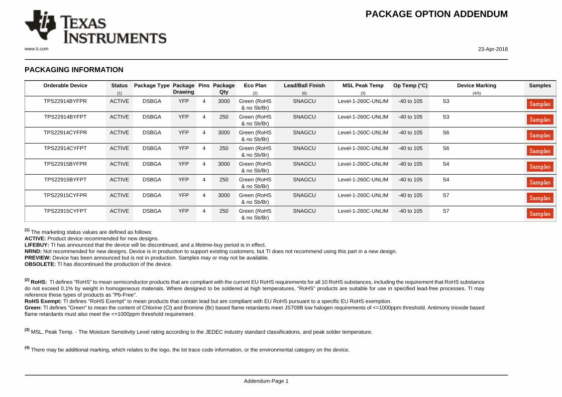
PACKAGING INFORMATION
Orderable Device Status(1)
Package Type PackageDrawing
Pins PackageQty
Eco Plan(2)
Lead/Ball Finish(6)
MSL Peak Temp(3)
Op Temp (°C) Device Marking(4/5)
Samples
TPS22914BYFPR ACTIVE DSBGA YFP 4 3000 Green (RoHS& no Sb/Br)
SNAGCU Level-1-260C-UNLIM -40 to 105 S3
TPS22914BYFPT ACTIVE DSBGA YFP 4 250 Green (RoHS& no Sb/Br)
SNAGCU Level-1-260C-UNLIM -40 to 105 S3
TPS22914CYFPR ACTIVE DSBGA YFP 4 3000 Green (RoHS& no Sb/Br)
SNAGCU Level-1-260C-UNLIM -40 to 105 S6
TPS22914CYFPT ACTIVE DSBGA YFP 4 250 Green (RoHS& no Sb/Br)
SNAGCU Level-1-260C-UNLIM -40 to 105 S6
TPS22915BYFPR ACTIVE DSBGA YFP 4 3000 Green (RoHS& no Sb/Br)
SNAGCU Level-1-260C-UNLIM -40 to 105 S4
TPS22915BYFPT ACTIVE DSBGA YFP 4 250 Green (RoHS& no Sb/Br)
SNAGCU Level-1-260C-UNLIM -40 to 105 S4
TPS22915CYFPR ACTIVE DSBGA YFP 4 3000 Green (RoHS& no Sb/Br)
SNAGCU Level-1-260C-UNLIM -40 to 105 S7
TPS22915CYFPT ACTIVE DSBGA YFP 4 250 Green (RoHS& no Sb/Br)
SNAGCU Level-1-260C-UNLIM -40 to 105 S7
(1) The marketing status values are defined as follows:ACTIVE: Product device recommended for new designs.LIFEBUY: TI has announced that the device will be discontinued, and a lifetime-buy period is in effect.NRND: Not recommended for new designs. Device is in production to support existing customers, but TI does not recommend using this part in a new design.PREVIEW: Device has been announced but is not in production. Samples may or may not be available.OBSOLETE: TI has discontinued the production of the device.
(2) RoHS: TI defines "RoHS" to mean semiconductor products that are compliant with the current EU RoHS requirements for all 10 RoHS substances, including the requirement that RoHS substancedo not exceed 0.1% by weight in homogeneous materials. Where designed to be soldered at high temperatures, "RoHS" products are suitable for use in specified lead-free processes. TI mayreference these types of products as "Pb-Free".RoHS Exempt: TI defines "RoHS Exempt" to mean products that contain lead but are compliant with EU RoHS pursuant to a specific EU RoHS exemption.Green: TI defines "Green" to mean the content of Chlorine (Cl) and Bromine (Br) based flame retardants meet JS709B low halogen requirements of <=1000ppm threshold. Antimony trioxide basedflame retardants must also meet the <=1000ppm threshold requirement.
(3) MSL, Peak Temp. - The Moisture Sensitivity Level rating according to the JEDEC industry standard classifications, and peak solder temperature.
(4) There may be additional marking, which relates to the logo, the lot trace code information, or the environmental category on the device.
PACKAGE OPTION ADDENDUM
www.ti.com 23-Apr-2018
Addendum-Page 2
(5) Multiple Device Markings will be inside parentheses. Only one Device Marking contained in parentheses and separated by a "~" will appear on a device. If a line is indented then it is a continuationof the previous line and the two combined represent the entire Device Marking for that device.
(6) Lead/Ball Finish - Orderable Devices may have multiple material finish options. Finish options are separated by a vertical ruled line. Lead/Ball Finish values may wrap to two lines if the finishvalue exceeds the maximum column width.
Important Information and Disclaimer:The information provided on this page represents TI's knowledge and belief as of the date that it is provided. TI bases its knowledge and belief on informationprovided by third parties, and makes no representation or warranty as to the accuracy of such information. Efforts are underway to better integrate information from third parties. TI has taken andcontinues to take reasonable steps to provide representative and accurate information but may not have conducted destructive testing or chemical analysis on incoming materials and chemicals.TI and TI suppliers consider certain information to be proprietary, and thus CAS numbers and other limited information may not be available for release.
In no event shall TI's liability arising out of such information exceed the total purchase price of the TI part(s) at issue in this document sold by TI to Customer on an annual basis.
TAPE AND REEL INFORMATION
*All dimensions are nominal
Device PackageType
PackageDrawing
Pins SPQ ReelDiameter
(mm)
ReelWidth
W1 (mm)
A0(mm)
B0(mm)
K0(mm)
P1(mm)
W(mm)
Pin1Quadrant
TPS22914BYFPR DSBGA YFP 4 3000 180.0 8.4 0.85 0.85 0.64 4.0 8.0 Q1
TPS22914BYFPR DSBGA YFP 4 3000 178.0 9.2 0.85 0.85 0.59 4.0 8.0 Q1
TPS22914BYFPT DSBGA YFP 4 250 178.0 9.2 0.85 0.85 0.59 4.0 8.0 Q1
TPS22914BYFPT DSBGA YFP 4 250 180.0 8.4 0.85 0.85 0.64 4.0 8.0 Q1
TPS22914CYFPR DSBGA YFP 4 3000 180.0 8.4 0.85 0.85 0.64 4.0 8.0 Q1
TPS22914CYFPT DSBGA YFP 4 250 180.0 8.4 0.85 0.85 0.64 4.0 8.0 Q1
TPS22915BYFPR DSBGA YFP 4 3000 178.0 9.2 0.85 0.85 0.59 4.0 8.0 Q1
TPS22915BYFPR DSBGA YFP 4 3000 180.0 8.4 0.85 0.85 0.64 4.0 8.0 Q1
TPS22915BYFPT DSBGA YFP 4 250 178.0 9.2 0.85 0.85 0.59 4.0 8.0 Q1
TPS22915CYFPR DSBGA YFP 4 3000 180.0 8.4 0.85 0.85 0.64 4.0 8.0 Q1
TPS22915CYFPT DSBGA YFP 4 250 180.0 8.4 0.85 0.85 0.64 4.0 8.0 Q1
PACKAGE MATERIALS INFORMATION
www.ti.com 10-May-2018
Pack Materials-Page 1
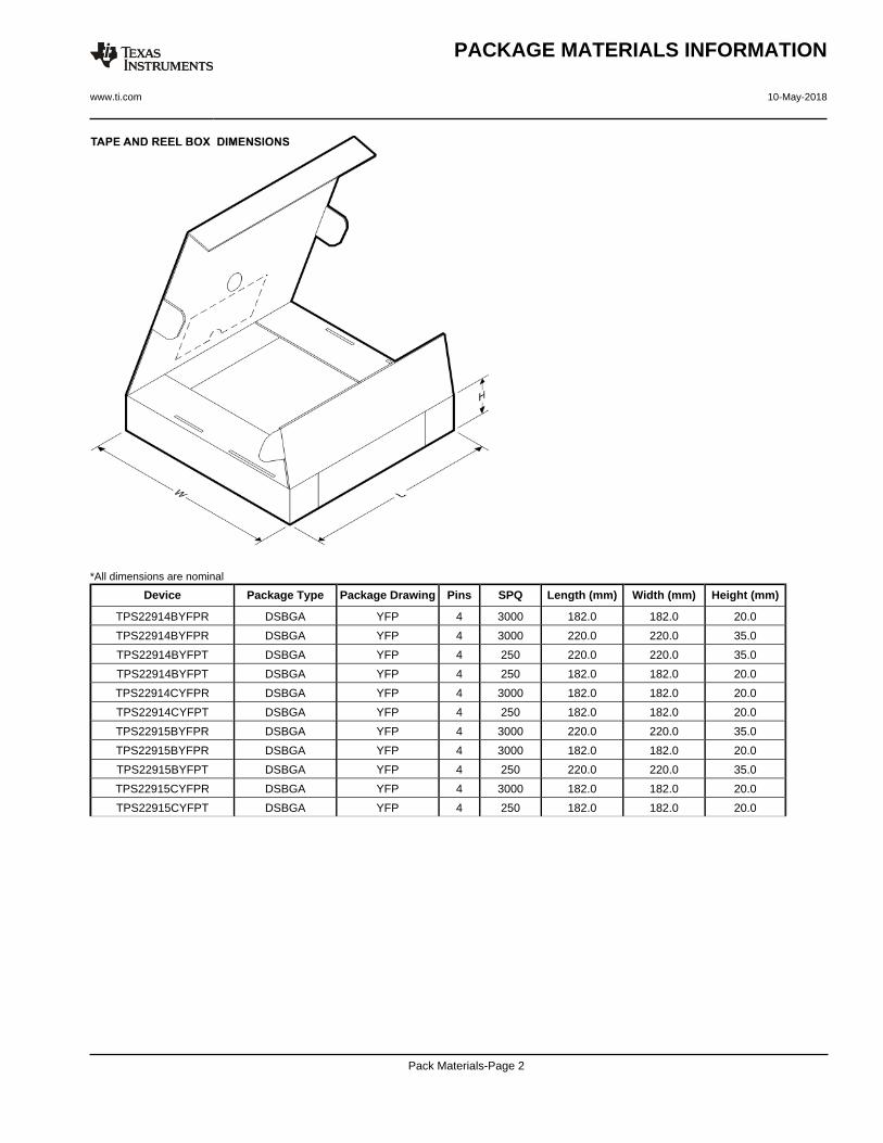
*All dimensions are nominal
Device Package Type Package Drawing Pins SPQ Length (mm) Width (mm) Height (mm)
TPS22914BYFPR DSBGA YFP 4 3000 182.0 182.0 20.0
TPS22914BYFPR DSBGA YFP 4 3000 220.0 220.0 35.0
TPS22914BYFPT DSBGA YFP 4 250 220.0 220.0 35.0
TPS22914BYFPT DSBGA YFP 4 250 182.0 182.0 20.0
TPS22914CYFPR DSBGA YFP 4 3000 182.0 182.0 20.0
TPS22914CYFPT DSBGA YFP 4 250 182.0 182.0 20.0
TPS22915BYFPR DSBGA YFP 4 3000 220.0 220.0 35.0
TPS22915BYFPR DSBGA YFP 4 3000 182.0 182.0 20.0
TPS22915BYFPT DSBGA YFP 4 250 220.0 220.0 35.0
TPS22915CYFPR DSBGA YFP 4 3000 182.0 182.0 20.0
TPS22915CYFPT DSBGA YFP 4 250 182.0 182.0 20.0
PACKAGE MATERIALS INFORMATION
www.ti.com 10-May-2018
Pack Materials-Page 2
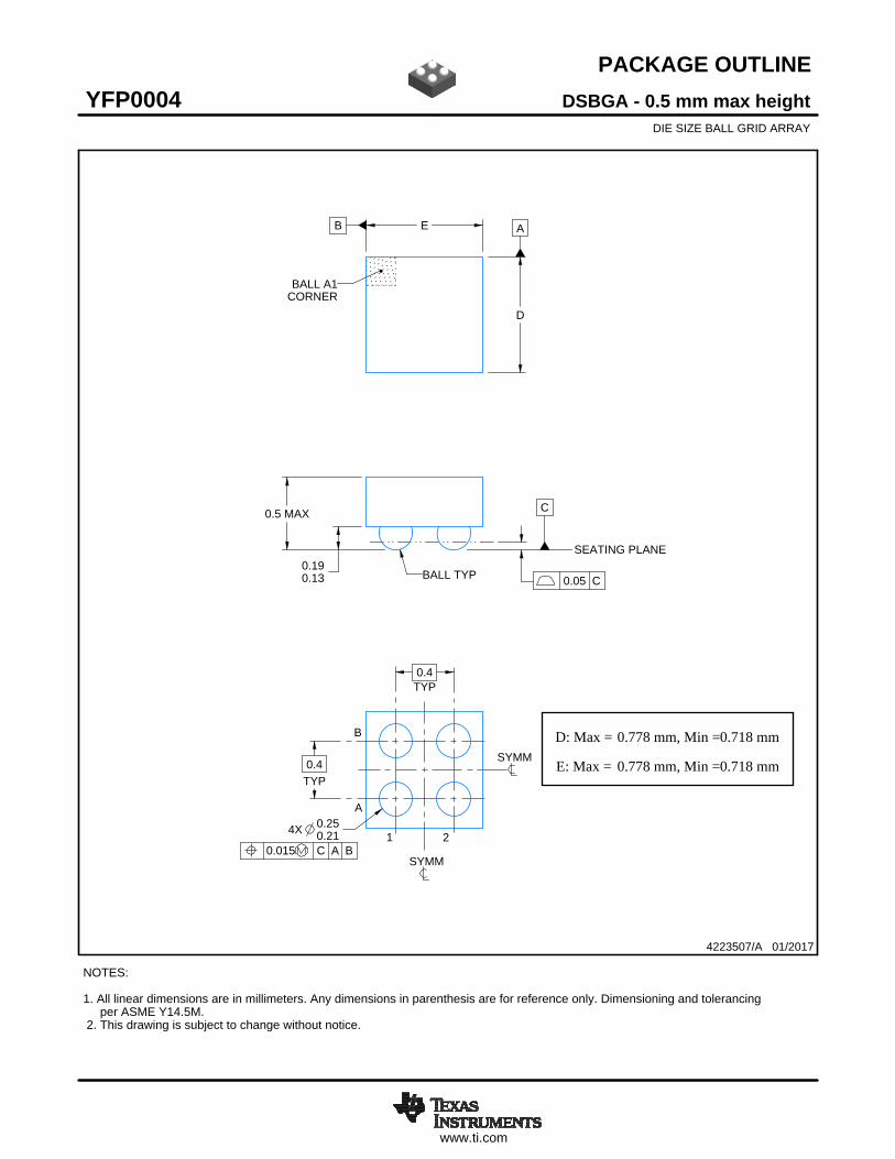
www.ti.com
PACKAGE OUTLINE
C0.5 MAX
0.190.13
0.4TYP
0.4TYP
4X 0.250.21
B E A
D
4223507/A 01/2017
DSBGA - 0.5 mm max heightYFP0004DIE SIZE BALL GRID ARRAY
NOTES: 1. All linear dimensions are in millimeters. Any dimensions in parenthesis are for reference only. Dimensioning and tolerancing per ASME Y14.5M. 2. This drawing is subject to change without notice.
BALL A1CORNER
SEATING PLANE
BALL TYP 0.05 C
A
B
20.015 C A B
SYMM
SYMM
1
SCALE 10.000
D: Max =
E: Max =
0.778 mm, Min =
0.778 mm, Min =
0.718 mm
0.718 mm
www.ti.com
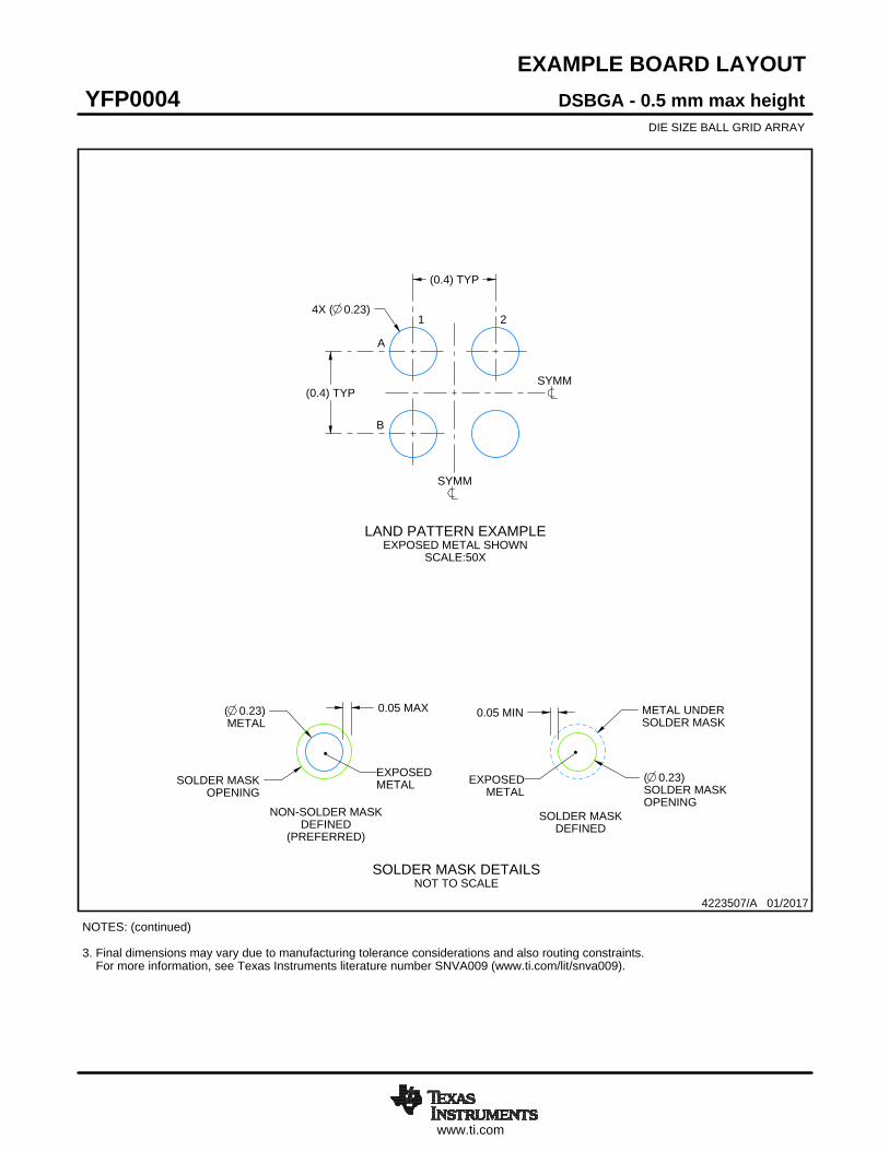
EXAMPLE BOARD LAYOUT
4X ( 0.23)
(0.4) TYP
(0.4) TYP
( 0.23)METAL
0.05 MAX
SOLDER MASKOPENING
METAL UNDERSOLDER MASK
( 0.23)SOLDER MASKOPENING
0.05 MIN
4223507/A 01/2017
DSBGA - 0.5 mm max heightYFP0004DIE SIZE BALL GRID ARRAY
NOTES: (continued) 3. Final dimensions may vary due to manufacturing tolerance considerations and also routing constraints. For more information, see Texas Instruments literature number SNVA009 (www.ti.com/lit/snva009).
SOLDER MASK DETAILSNOT TO SCALE
SYMM
SYMM
LAND PATTERN EXAMPLEEXPOSED METAL SHOWN
SCALE:50X
A
B
1 2
NON-SOLDER MASKDEFINED
(PREFERRED)
EXPOSEDMETAL
SOLDER MASKDEFINED
EXPOSEDMETAL
www.ti.com
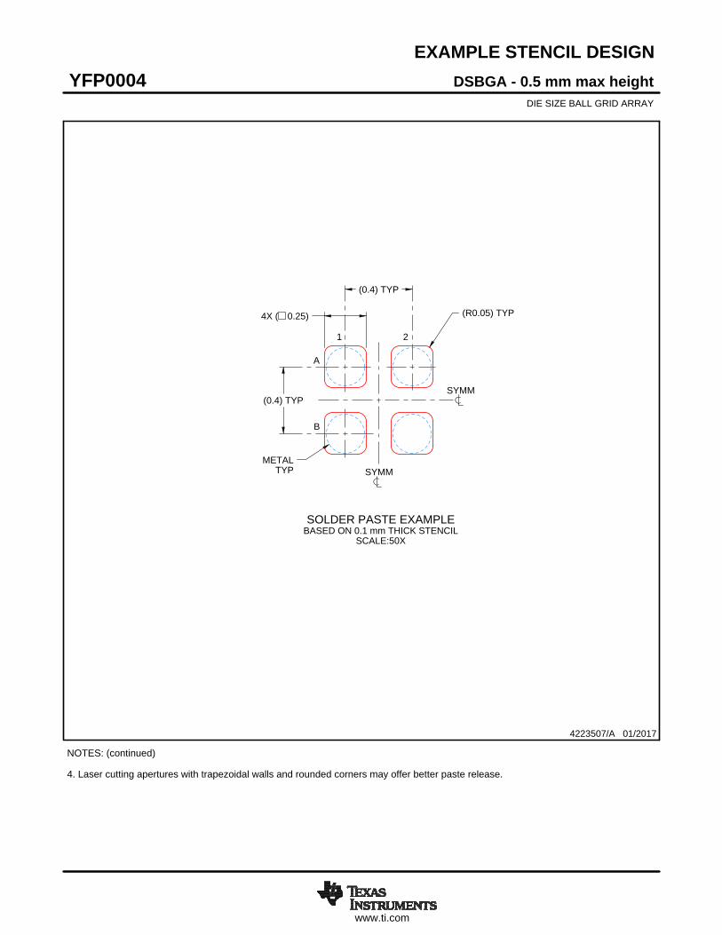
EXAMPLE STENCIL DESIGN
(0.4) TYP
(0.4) TYP
4X ( 0.25) (R0.05) TYP
METALTYP
4223507/A 01/2017
DSBGA - 0.5 mm max heightYFP0004DIE SIZE BALL GRID ARRAY
NOTES: (continued) 4. Laser cutting apertures with trapezoidal walls and rounded corners may offer better paste release.
SYMM
SYMM
SOLDER PASTE EXAMPLEBASED ON 0.1 mm THICK STENCIL
SCALE:50X
A
B
1 2
IMPORTANT NOTICE
Texas Instruments Incorporated (TI) reserves the right to make corrections, enhancements, improvements and other changes to itssemiconductor products and services per JESD46, latest issue, and to discontinue any product or service per JESD48, latest issue. Buyersshould obtain the latest relevant information before placing orders and should verify that such information is current and complete.TI’s published terms of sale for semiconductor products (http://www.ti.com/sc/docs/stdterms.htm) apply to the sale of packaged integratedcircuit products that TI has qualified and released to market. Additional terms may apply to the use or sale of other types of TI products andservices.Reproduction of significant portions of TI information in TI data sheets is permissible only if reproduction is without alteration and isaccompanied by all associated warranties, conditions, limitations, and notices. TI is not responsible or liable for such reproduceddocumentation. Information of third parties may be subject to additional restrictions. Resale of TI products or services with statementsdifferent from or beyond the parameters stated by TI for that product or service voids all express and any implied warranties for theassociated TI product or service and is an unfair and deceptive business practice. TI is not responsible or liable for any such statements.Buyers and others who are developing systems that incorporate TI products (collectively, “Designers”) understand and agree that Designersremain responsible for using their independent analysis, evaluation and judgment in designing their applications and that Designers havefull and exclusive responsibility to assure the safety of Designers' applications and compliance of their applications (and of all TI productsused in or for Designers’ applications) with all applicable regulations, laws and other applicable requirements. Designer represents that, withrespect to their applications, Designer has all the necessary expertise to create and implement safeguards that (1) anticipate dangerousconsequences of failures, (2) monitor failures and their consequences, and (3) lessen the likelihood of failures that might cause harm andtake appropriate actions. Designer agrees that prior to using or distributing any applications that include TI products, Designer willthoroughly test such applications and the functionality of such TI products as used in such applications.TI’s provision of technical, application or other design advice, quality characterization, reliability data or other services or information,including, but not limited to, reference designs and materials relating to evaluation modules, (collectively, “TI Resources”) are intended toassist designers who are developing applications that incorporate TI products; by downloading, accessing or using TI Resources in anyway, Designer (individually or, if Designer is acting on behalf of a company, Designer’s company) agrees to use any particular TI Resourcesolely for this purpose and subject to the terms of this Notice.TI’s provision of TI Resources does not expand or otherwise alter TI’s applicable published warranties or warranty disclaimers for TIproducts, and no additional obligations or liabilities arise from TI providing such TI Resources. TI reserves the right to make corrections,enhancements, improvements and other changes to its TI Resources. TI has not conducted any testing other than that specificallydescribed in the published documentation for a particular TI Resource.Designer is authorized to use, copy and modify any individual TI Resource only in connection with the development of applications thatinclude the TI product(s) identified in such TI Resource. NO OTHER LICENSE, EXPRESS OR IMPLIED, BY ESTOPPEL OR OTHERWISETO ANY OTHER TI INTELLECTUAL PROPERTY RIGHT, AND NO LICENSE TO ANY TECHNOLOGY OR INTELLECTUAL PROPERTYRIGHT OF TI OR ANY THIRD PARTY IS GRANTED HEREIN, including but not limited to any patent right, copyright, mask work right, orother intellectual property right relating to any combination, machine, or process in which TI products or services are used. Informationregarding or referencing third-party products or services does not constitute a license to use such products or services, or a warranty orendorsement thereof. Use of TI Resources may require a license from a third party under the patents or other intellectual property of thethird party, or a license from TI under the patents or other intellectual property of TI.TI RESOURCES ARE PROVIDED “AS IS” AND WITH ALL FAULTS. TI DISCLAIMS ALL OTHER WARRANTIES ORREPRESENTATIONS, EXPRESS OR IMPLIED, REGARDING RESOURCES OR USE THEREOF, INCLUDING BUT NOT LIMITED TOACCURACY OR COMPLETENESS, TITLE, ANY EPIDEMIC FAILURE WARRANTY AND ANY IMPLIED WARRANTIES OFMERCHANTABILITY, FITNESS FOR A PARTICULAR PURPOSE, AND NON-INFRINGEMENT OF ANY THIRD PARTY INTELLECTUALPROPERTY RIGHTS. TI SHALL NOT BE LIABLE FOR AND SHALL NOT DEFEND OR INDEMNIFY DESIGNER AGAINST ANY CLAIM,INCLUDING BUT NOT LIMITED TO ANY INFRINGEMENT CLAIM THAT RELATES TO OR IS BASED ON ANY COMBINATION OFPRODUCTS EVEN IF DESCRIBED IN TI RESOURCES OR OTHERWISE. IN NO EVENT SHALL TI BE LIABLE FOR ANY ACTUAL,DIRECT, SPECIAL, COLLATERAL, INDIRECT, PUNITIVE, INCIDENTAL, CONSEQUENTIAL OR EXEMPLARY DAMAGES INCONNECTION WITH OR ARISING OUT OF TI RESOURCES OR USE THEREOF, AND REGARDLESS OF WHETHER TI HAS BEENADVISED OF THE POSSIBILITY OF SUCH DAMAGES.Unless TI has explicitly designated an individual product as meeting the requirements of a particular industry standard (e.g., ISO/TS 16949and ISO 26262), TI is not responsible for any failure to meet such industry standard requirements.Where TI specifically promotes products as facilitating functional safety or as compliant with industry functional safety standards, suchproducts are intended to help enable customers to design and create their own applications that meet applicable functional safety standardsand requirements. Using products in an application does not by itself establish any safety features in the application. Designers mustensure compliance with safety-related requirements and standards applicable to their applications. Designer may not use any TI products inlife-critical medical equipment unless authorized officers of the parties have executed a special contract specifically governing such use.Life-critical medical equipment is medical equipment where failure of such equipment would cause serious bodily injury or death (e.g., lifesupport, pacemakers, defibrillators, heart pumps, neurostimulators, and implantables). Such equipment includes, without limitation, allmedical devices identified by the U.S. Food and Drug Administration as Class III devices and equivalent classifications outside the U.S.TI may expressly designate certain products as completing a particular qualification (e.g., Q100, Military Grade, or Enhanced Product).Designers agree that it has the necessary expertise to select the product with the appropriate qualification designation for their applicationsand that proper product selection is at Designers’ own risk. Designers are solely responsible for compliance with all legal and regulatoryrequirements in connection with such selection.Designer will fully indemnify TI and its representatives against any damages, costs, losses, and/or liabilities arising out of Designer’s non-compliance with the terms and provisions of this Notice.
Mailing Address: Texas Instruments, Post Office Box 655303, Dallas, Texas 75265Copyright © 2018, Texas Instruments Incorporated


![C C!C!C B]B B¥BlB·BrB¢B®B B¤B~B B BdB·B - Fujitsu...C C!C!C B]B B¥BlB·BrB¢B®B1.3. B 4?" B 1 !ªB1 2 ¸ {AîBpB·B Bt / 0 C C!C!C Ñ!ª(*B1 Ñ " H 0 B BpB·B Bt Ñ!ª o 0](https://img.pdfslide.net/doc/110x75/60a9b5ef1dcf032ca5305f6d/c-ccc-bb-bblbbrbbb-bbb-b-bdbb-fujitsu-c-ccc-bb-bblbbrbbb13.jpg)