Embed Size (px)
Citation preview
OUT
GNDFAULT
ILIM_LO
EN
RILIM_LO
RSTATUS
(10 kW)
Power Switch EN
4.5V – 5.5V
TPS2546
0.1 uF
CUSB
Fault Signal
DM_IN
DP_IN
VBUS
D-
D+
GND
USB
Connector
To Portable Device à
Power Bus
CTL1
CTL2
CTL3
ILIM_SELILIM Select
DM_OUT
DP_OUT To Host Controller àMode Select I/O
IN
STATUSSTATUS Signal
RILIM_HI
ILIM_HI
RFAULT
(10 kW)
Copyright © 2016, Texas Instruments Incorporated
Product
Folder
Sample &Buy
Technical
Documents
Tools &
Software
Support &Community
An IMPORTANT NOTICE at the end of this data sheet addresses availability, warranty, changes, use in safety-critical applications,intellectual property matters and other important disclaimers. PRODUCTION DATA.
TPS2546SLVSBJ2C –FEBRUARY 2013–REVISED JULY 2016
TPS2546 USB Charging Port Controller and Power Switch With Load Detection
1
1 Features1• D+/D– CDP/DCP Modes per USB Battery
Charging Specification 1.2• D+/D– Shorted Mode per Chinese
Telecommunication Industry Standard YD/T1591-2009
• Supports Non-BC1.2 Charging Modes byAutomatic Selection:– D+/D– Divider Modes 2 V/2.7 V and 2.7 V/2 V– D+/D– 1.2-V Mode
• Supports Sleep-Mode Charging andMouse/Keyboard Wakeup
• Automatic SDP/CDP Switching for Devices ThatDo Not Connect to CDP Ports
• Load Detection for Power Supply Control in S4/S5Charging and Port Power Management in AllCharge Modes
• Compatible With USB 2.0 and 3.0 Power SwitchRequirements
• Integrated 73-mΩ (Typical) High-Side MOSFET• Adjustable Current-Limit up to 3 A (Typical)• Operating Range: 4.5 V to 5.5 V• Max Device Current:
– 2 µA When Device Disabled– 270 µA When Device Enabled
• Drop-In and BOM Compatible With TPS2543• Available in 16-Pin WQFN (3.00 mm × 3.00 mm)
Package• 8-kV ESD Rating on DM/DP Pins• UL Listed File No. E169910 and CB certified
2 Applications• USB Ports (Host and Hubs)• Notebook and Desktop PCs• Universal Wall-Charging Adapters
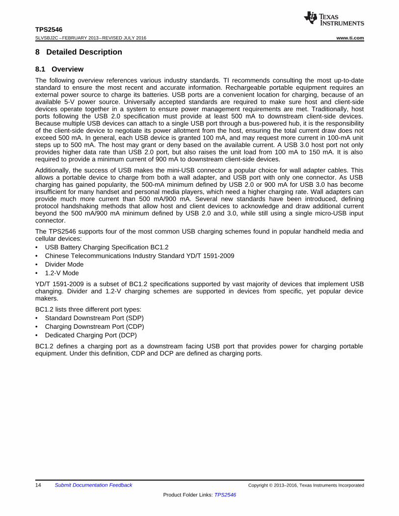
3 DescriptionThe TPS2546 is a USB charging port controller andpower switch with an integrated USB 2.0 high-speeddata line (D+/D–) switch. TPS2546 provides theelectrical signatures on D+/D– to support chargingschemes listed under Feature Description. TI testscharging of popular mobile phones, tablets, andmedia devices with the TPS2546 to ensurecompatibility with both BC1.2 compliant, and non-BC1.2 compliant devices.
In addition to charging popular devices, the TPS2546also supports two distinct power managementfeatures, namely, power wake and port powermanagement (PPM) through the STATUS pin. Powerwake allows for power supply control in S4/S5charging and PPM the ability to manage port power ina multi-port application. Additionally, system wake up(from S3) with a mouse/keyboard (both low speedand full speed) is fully supported in the TPS2546.
The TPS2546 73-mΩ power-distribution switch isintended for applications where heavy capacitiveloads and short-circuits are likely to be encountered.Two programmable current thresholds provideflexibility for setting current limits and load detectthresholds.
Device Information(1)
PART NUMBER PACKAGE BODY SIZE (NOM)TPS2546 WQFN (16) 3.00 mm × 3.00 mm
(1) For all available packages, see the orderable addendum atthe end of the data sheet.
Simplified Schematic
2
TPS2546SLVSBJ2C –FEBRUARY 2013–REVISED JULY 2016 www.ti.com
Product Folder Links: TPS2546
Submit Documentation Feedback Copyright © 2013–2016, Texas Instruments Incorporated
Table of Contents1 Features .................................................................. 12 Applications ........................................................... 13 Description ............................................................. 14 Revision History..................................................... 25 Pin Configuration and Functions ......................... 36 Specifications......................................................... 4
6.1 Absolute Maximum Ratings ...................................... 46.2 ESD Ratings.............................................................. 46.3 Recommended Operating Conditions....................... 46.4 Thermal Information .................................................. 56.5 Electrical Characteristics........................................... 56.6 Electrical Characteristics: High-Bandwidth Switch.... 66.7 Electrical Characteristics: Charging Controller ......... 76.8 Typical Characteristics .............................................. 9
7 Parameter Measurement Information ................ 138 Detailed Description ............................................ 14
8.1 Overview ................................................................. 148.2 Functional Block Diagram ....................................... 15
8.3 Feature Description................................................. 158.4 Device Functional Modes........................................ 26
9 Application and Implementation ........................ 299.1 Application Information............................................ 299.2 Typical Application .................................................. 30
10 Power Supply Recommendations ..................... 3311 Layout................................................................... 33
11.1 Layout Guidelines ................................................. 3311.2 Layout Example .................................................... 34
12 Device and Documentation Support ................. 3512.1 Documentation Support ....................................... 3512.2 Receiving Notification of Documentation Updates 3512.3 Community Resources.......................................... 3512.4 Trademarks ........................................................... 3512.5 Electrostatic Discharge Caution............................ 3512.6 Glossary ................................................................ 35
13 Mechanical, Packaging, and OrderableInformation ........................................................... 35
4 Revision HistoryNOTE: Page numbers for previous revisions may differ from page numbers in the current version.
Changes from Revision B (January 2016) to Revision C Page
• Corrected references to images in the Feature Description section .................................................................................... 15• Added text to the Layout Guidelines section ........................................................................................................................ 34
Changes from Revision A (Febuary 2013) to Revision B Page
• Added ESD Ratings table, Feature Description section, Device Functional Modes, Application and Implementationsection, Power Supply Recommendations section, Layout section, Device and Documentation Support section, andMechanical, Packaging, and Orderable Information section. ................................................................................................. 1
Changes from Original (February 2013) to Revision A Page
• Changed the device From: Preview To: Production............................................................................................................... 1
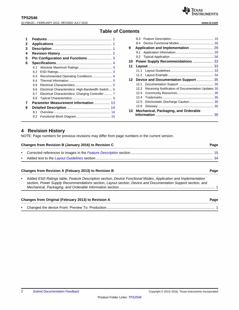
1
2
3
4
5 6 7 8
9
10
11
12
13141516
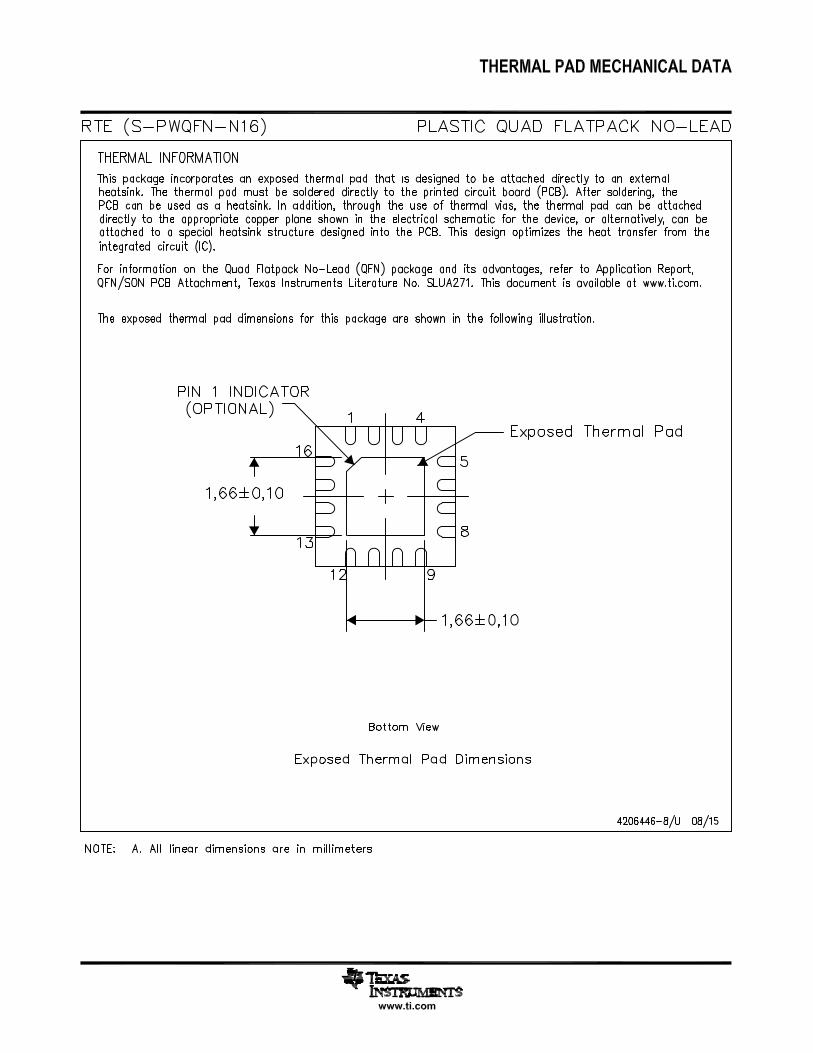
Thermal Pad
IN
DM_OUT
DP_OUT
ILIM_SEL
EN
CLT
1
CLT
2
CLT
3
OUT
DM_IN
DP_IN
STATUS
ILIM
_H
I
ILIM
_LO
GN
D
FA
ULT
3
TPS2546www.ti.com SLVSBJ2C –FEBRUARY 2013–REVISED JULY 2016
Product Folder Links: TPS2546
Submit Documentation FeedbackCopyright © 2013–2016, Texas Instruments Incorporated
(1) G = ground, I = input, O = output, P = power.
5 Pin Configuration and Functions
RTE Package16-Pin WQFN
Top View
Pin FunctionsPIN
TYPE (1) DESCRIPTIONNO. NAME
1 IN P Input voltage and supply voltage; connect 0.1 μF or greater ceramic capacitor from IN to GND as closeto the device as possible.
2 DM_OUT I/O D– data line to USB host controller.3 DP_OUT I/O D+ data line to USB host controller.
4 ILIM_SEL I Logic-level input signal used to control the charging mode, current limit threshold, and load detection;see Table 3. Can be tied directly to IN or GND without pullup or pulldown resistor.
5 EN ILogic-level input for turning the power switch and the signal switches on/off; logic low turns off the signaland power switches and holds OUT in discharge. Can be tied directly to IN or GND without pullup orpulldown resistor.
6 CTL1 ILogic-level inputs used to control the charging mode and the signal switches; see Table 3. Can be tieddirectly to IN or GND without pullup or pulldown resistor.7 CTL2 I
8 CTL3 I9 STATUS O Active-low open-drain output, asserted in load detection conditions.10 DP_IN I/O D+ data line to downstream connector.11 DM_IN I/O D– data line to downstream connector.12 OUT P Power-switch output.13 FAULT O Active-low open-drain output, asserted during overtemperature or current limit conditions.14 GND P Ground connection.
15 ILIM_LO I External resistor connection used to set the low current-limit threshold and the load detection currentthreshold. A resistor to ILIM_LO is optional; see Current-Limit Settings in Detailed Description.
16 ILIM_HI I External resistor connection used to set the high-current-limit threshold.
— ThermalPad — Internally connected to GND; used to heatsink the part to the circuit board traces. Connect to GND
plane.
4
TPS2546SLVSBJ2C –FEBRUARY 2013–REVISED JULY 2016 www.ti.com
Product Folder Links: TPS2546
Submit Documentation Feedback Copyright © 2013–2016, Texas Instruments Incorporated
(1) Stresses beyond those listed under Absolute Maximum Ratings may cause permanent damage to the device. These are stress ratingsonly, which do not imply functional operation of the device at these or any other conditions beyond those indicated under RecommendedOperating Conditions. Exposure to absolute-maximum-rated conditions for extended periods may affect device reliability.
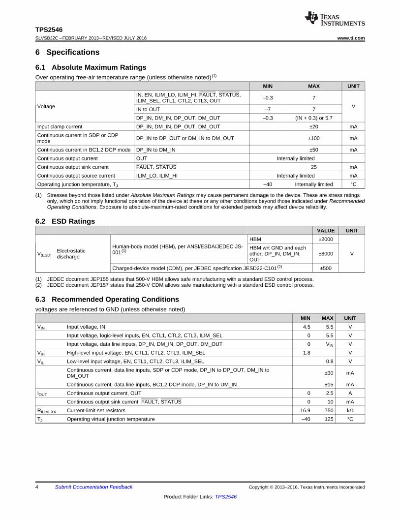
6 Specifications
6.1 Absolute Maximum RatingsOver operating free-air temperature range (unless otherwise noted) (1)
MIN MAX UNIT
Voltage
IN, EN, ILIM_LO, ILIM_HI, FAULT, STATUS,ILIM_SEL, CTL1, CTL2, CTL3, OUT –0.3 7
VIN to OUT –7 7DP_IN, DM_IN, DP_OUT, DM_OUT –0.3 (IN + 0.3) or 5.7
Input clamp current DP_IN, DM_IN, DP_OUT, DM_OUT ±20 mAContinuous current in SDP or CDPmode DP_IN to DP_OUT or DM_IN to DM_OUT ±100 mA
Continuous current in BC1.2 DCP mode DP_IN to DM_IN ±50 mAContinuous output current OUT Internally limitedContinuous output sink current FAULT, STATUS 25 mAContinuous output source current ILIM_LO, ILIM_HI Internally limited mAOperating junction temperature, TJ –40 Internally limited °C
(1) JEDEC document JEP155 states that 500-V HBM allows safe manufacturing with a standard ESD control process.(2) JEDEC document JEP157 states that 250-V CDM allows safe manufacturing with a standard ESD control process.
6.2 ESD RatingsVALUE UNIT
V(ESD)Electrostaticdischarge
Human-body model (HBM), per ANSI/ESDA/JEDEC JS-001 (1)
HBM ±2000
VHBM wrt GND and eachother, DP_IN, DM_IN,OUT
±8000
Charged-device model (CDM), per JEDEC specification JESD22-C101 (2) ±500
6.3 Recommended Operating Conditionsvoltages are referenced to GND (unless otherwise noted)
MIN MAX UNITVIN Input voltage, IN 4.5 5.5 V
Input voltage, logic-level inputs, EN, CTL1, CTL2, CTL3, ILIM_SEL 0 5.5 VInput voltage, data line inputs, DP_IN, DM_IN, DP_OUT, DM_OUT 0 VIN V
VIH High-level input voltage, EN, CTL1, CTL2, CTL3, ILIM_SEL 1.8 VVIL Low-level input voltage, EN, CTL1, CTL2, CTL3, ILIM_SEL 0.8 V
Continuous current, data line inputs, SDP or CDP mode, DP_IN to DP_OUT, DM_IN toDM_OUT ±30 mA
Continuous current, data line inputs, BC1.2 DCP mode, DP_IN to DM_IN ±15 mAIOUT Continuous output current, OUT 0 2.5 A
Continuous output sink current, FAULT, STATUS 0 10 mARILIM_XX Current-limit set resistors 16.9 750 kΩTJ Operating virtual junction temperature –40 125 °C
5
TPS2546www.ti.com SLVSBJ2C –FEBRUARY 2013–REVISED JULY 2016
Product Folder Links: TPS2546
Submit Documentation FeedbackCopyright © 2013–2016, Texas Instruments Incorporated
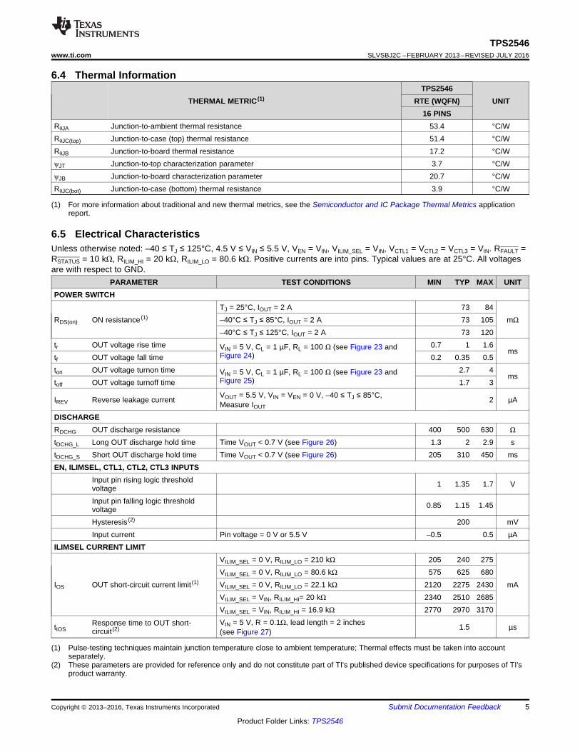
(1) For more information about traditional and new thermal metrics, see the Semiconductor and IC Package Thermal Metrics applicationreport.
6.4 Thermal Information
THERMAL METRIC (1)TPS2546
UNITRTE (WQFN)16 PINS
RθJA Junction-to-ambient thermal resistance 53.4 °C/WRθJC(top) Junction-to-case (top) thermal resistance 51.4 °C/WRθJB Junction-to-board thermal resistance 17.2 °C/WψJT Junction-to-top characterization parameter 3.7 °C/WψJB Junction-to-board characterization parameter 20.7 °C/WRθJC(bot) Junction-to-case (bottom) thermal resistance 3.9 °C/W
(1) Pulse-testing techniques maintain junction temperature close to ambient temperature; Thermal effects must be taken into accountseparately.
(2) These parameters are provided for reference only and do not constitute part of TI's published device specifications for purposes of TI'sproduct warranty.
6.5 Electrical CharacteristicsUnless otherwise noted: –40 ≤ TJ ≤ 125°C, 4.5 V ≤ VIN ≤ 5.5 V, VEN = VIN, VILIM_SEL = VIN, VCTL1 = VCTL2 = VCTL3 = VIN. RFAULT =RSTATUS = 10 kΩ, RILIM_HI = 20 kΩ, RILIM_LO = 80.6 kΩ. Positive currents are into pins. Typical values are at 25°C. All voltagesare with respect to GND.
PARAMETER TEST CONDITIONS MIN TYP MAX UNITPOWER SWITCH
RDS(on) ON resistance (1)
TJ = 25°C, IOUT = 2 A 73 84mΩ–40°C ≤ TJ ≤ 85°C, IOUT = 2 A 73 105
–40°C ≤ TJ ≤ 125°C, IOUT = 2 A 73 120tr OUT voltage rise time VIN = 5 V, CL = 1 µF, RL = 100 Ω (see Figure 23 and
Figure 24)0.7 1 1.6
mstf OUT voltage fall time 0.2 0.35 0.5ton OUT voltage turnon time VIN = 5 V, CL = 1 µF, RL = 100 Ω (see Figure 23 and
Figure 25)2.7 4
mstoff OUT voltage turnoff time 1.7 3
IREV Reverse leakage current VOUT = 5.5 V, VIN = VEN = 0 V, –40 ≤ TJ ≤ 85°C,Measure IOUT
2 µA
DISCHARGERDCHG OUT discharge resistance 400 500 630 Ω
tDCHG_L Long OUT discharge hold time Time VOUT < 0.7 V (see Figure 26) 1.3 2 2.9 stDCHG_S Short OUT discharge hold time Time VOUT < 0.7 V (see Figure 26) 205 310 450 msEN, ILIMSEL, CTL1, CTL2, CTL3 INPUTS
Input pin rising logic thresholdvoltage 1 1.35 1.7 V
Input pin falling logic thresholdvoltage 0.85 1.15 1.45
Hysteresis (2) 200 mVInput current Pin voltage = 0 V or 5.5 V –0.5 0.5 µA
ILIMSEL CURRENT LIMIT
IOS OUT short-circuit current limit (1)
VILIM_SEL = 0 V, RILIM_LO = 210 kΩ 205 240 275
mAVILIM_SEL = 0 V, RILIM_LO = 80.6 kΩ 575 625 680VILIM_SEL = 0 V, RILIM_LO = 22.1 kΩ 2120 2275 2430VILIM_SEL = VIN, RILIM_HI= 20 kΩ 2340 2510 2685VILIM_SEL = VIN, RILIM_HI = 16.9 kΩ 2770 2970 3170
tIOSResponse time to OUT short-circuit (2)
VIN = 5 V, R = 0.1Ω, lead length = 2 inches(see Figure 27) 1.5 µs
6
TPS2546SLVSBJ2C –FEBRUARY 2013–REVISED JULY 2016 www.ti.com
Product Folder Links: TPS2546
Submit Documentation Feedback Copyright © 2013–2016, Texas Instruments Incorporated
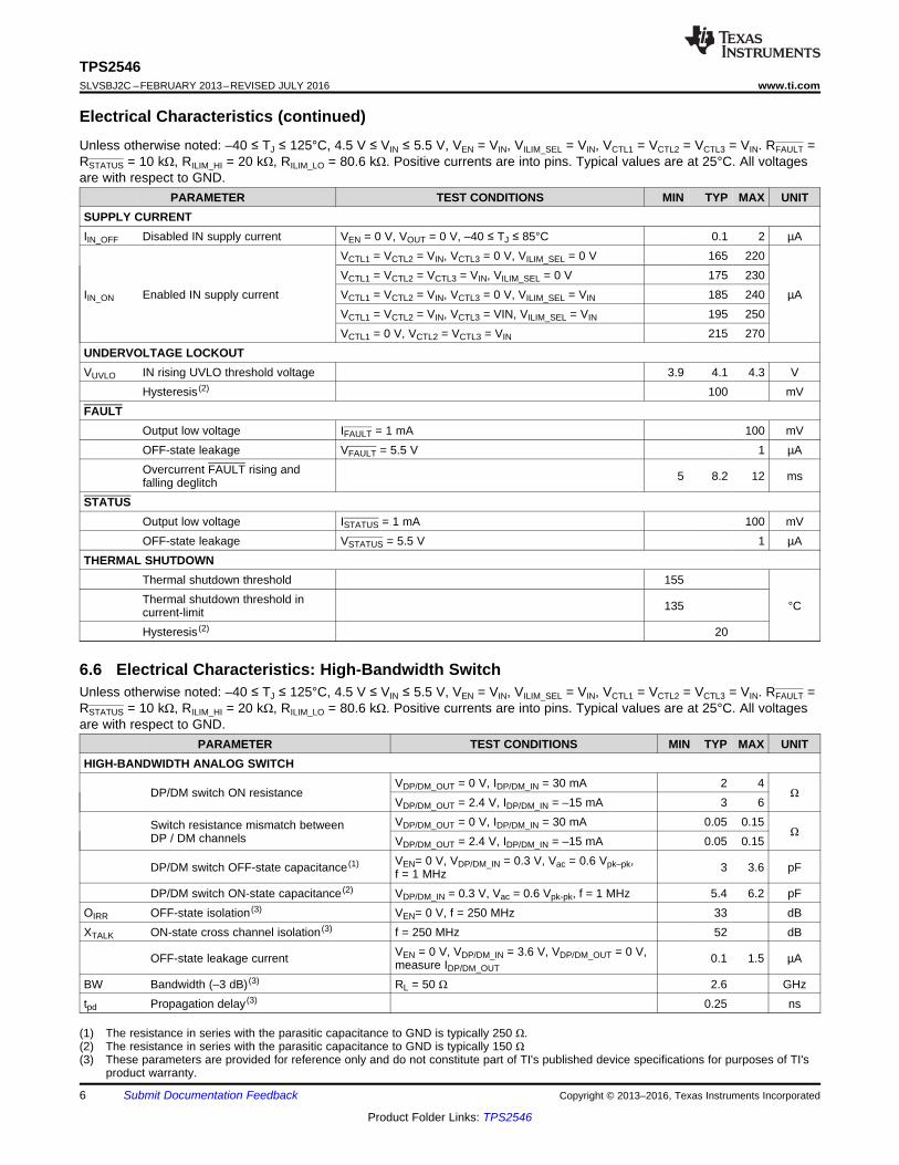
Electrical Characteristics (continued)Unless otherwise noted: –40 ≤ TJ ≤ 125°C, 4.5 V ≤ VIN ≤ 5.5 V, VEN = VIN, VILIM_SEL = VIN, VCTL1 = VCTL2 = VCTL3 = VIN. RFAULT =RSTATUS = 10 kΩ, RILIM_HI = 20 kΩ, RILIM_LO = 80.6 kΩ. Positive currents are into pins. Typical values are at 25°C. All voltagesare with respect to GND.
PARAMETER TEST CONDITIONS MIN TYP MAX UNITSUPPLY CURRENTIIN_OFF Disabled IN supply current VEN = 0 V, VOUT = 0 V, –40 ≤ TJ ≤ 85°C 0.1 2 µA
IIN_ON Enabled IN supply current
VCTL1 = VCTL2 = VIN, VCTL3 = 0 V, VILIM_SEL = 0 V 165 220
µAVCTL1 = VCTL2 = VCTL3 = VIN, VILIM_SEL = 0 V 175 230VCTL1 = VCTL2 = VIN, VCTL3 = 0 V, VILIM_SEL = VIN 185 240VCTL1 = VCTL2 = VIN, VCTL3 = VIN, VILIM_SEL = VIN 195 250VCTL1 = 0 V, VCTL2 = VCTL3 = VIN 215 270
UNDERVOLTAGE LOCKOUTVUVLO IN rising UVLO threshold voltage 3.9 4.1 4.3 V
Hysteresis (2) 100 mVFAULT
Output low voltage IFAULT = 1 mA 100 mVOFF-state leakage VFAULT = 5.5 V 1 µAOvercurrent FAULT rising andfalling deglitch 5 8.2 12 ms
STATUSOutput low voltage ISTATUS = 1 mA 100 mVOFF-state leakage VSTATUS = 5.5 V 1 µA
THERMAL SHUTDOWNThermal shutdown threshold 155
°CThermal shutdown threshold incurrent-limit 135
Hysteresis (2) 20
(1) The resistance in series with the parasitic capacitance to GND is typically 250 Ω.(2) The resistance in series with the parasitic capacitance to GND is typically 150 Ω(3) These parameters are provided for reference only and do not constitute part of TI's published device specifications for purposes of TI's
product warranty.
6.6 Electrical Characteristics: High-Bandwidth SwitchUnless otherwise noted: –40 ≤ TJ ≤ 125°C, 4.5 V ≤ VIN ≤ 5.5 V, VEN = VIN, VILIM_SEL = VIN, VCTL1 = VCTL2 = VCTL3 = VIN. RFAULT =RSTATUS = 10 kΩ, RILIM_HI = 20 kΩ, RILIM_LO = 80.6 kΩ. Positive currents are into pins. Typical values are at 25°C. All voltagesare with respect to GND.
PARAMETER TEST CONDITIONS MIN TYP MAX UNITHIGH-BANDWIDTH ANALOG SWITCH
DP/DM switch ON resistanceVDP/DM_OUT = 0 V, IDP/DM_IN = 30 mA 2 4
ΩVDP/DM_OUT = 2.4 V, IDP/DM_IN = –15 mA 3 6
Switch resistance mismatch betweenDP / DM channels
VDP/DM_OUT = 0 V, IDP/DM_IN = 30 mA 0.05 0.15Ω
VDP/DM_OUT = 2.4 V, IDP/DM_IN = –15 mA 0.05 0.15
DP/DM switch OFF-state capacitance (1) VEN= 0 V, VDP/DM_IN = 0.3 V, Vac = 0.6 Vpk–pk,f = 1 MHz 3 3.6 pF
DP/DM switch ON-state capacitance (2) VDP/DM_IN = 0.3 V, Vac = 0.6 Vpk-pk, f = 1 MHz 5.4 6.2 pFOIRR OFF-state isolation (3) VEN= 0 V, f = 250 MHz 33 dBXTALK ON-state cross channel isolation (3) f = 250 MHz 52 dB
OFF-state leakage current VEN = 0 V, VDP/DM_IN = 3.6 V, VDP/DM_OUT = 0 V,measure IDP/DM_OUT
0.1 1.5 µA
BW Bandwidth (–3 dB) (3) RL = 50 Ω 2.6 GHztpd Propagation delay (3) 0.25 ns
7
TPS2546www.ti.com SLVSBJ2C –FEBRUARY 2013–REVISED JULY 2016
Product Folder Links: TPS2546
Submit Documentation FeedbackCopyright © 2013–2016, Texas Instruments Incorporated
Electrical Characteristics: High-Bandwidth Switch (continued)Unless otherwise noted: –40 ≤ TJ ≤ 125°C, 4.5 V ≤ VIN ≤ 5.5 V, VEN = VIN, VILIM_SEL = VIN, VCTL1 = VCTL2 = VCTL3 = VIN. RFAULT =RSTATUS = 10 kΩ, RILIM_HI = 20 kΩ, RILIM_LO = 80.6 kΩ. Positive currents are into pins. Typical values are at 25°C. All voltagesare with respect to GND.
PARAMETER TEST CONDITIONS MIN TYP MAX UNIT
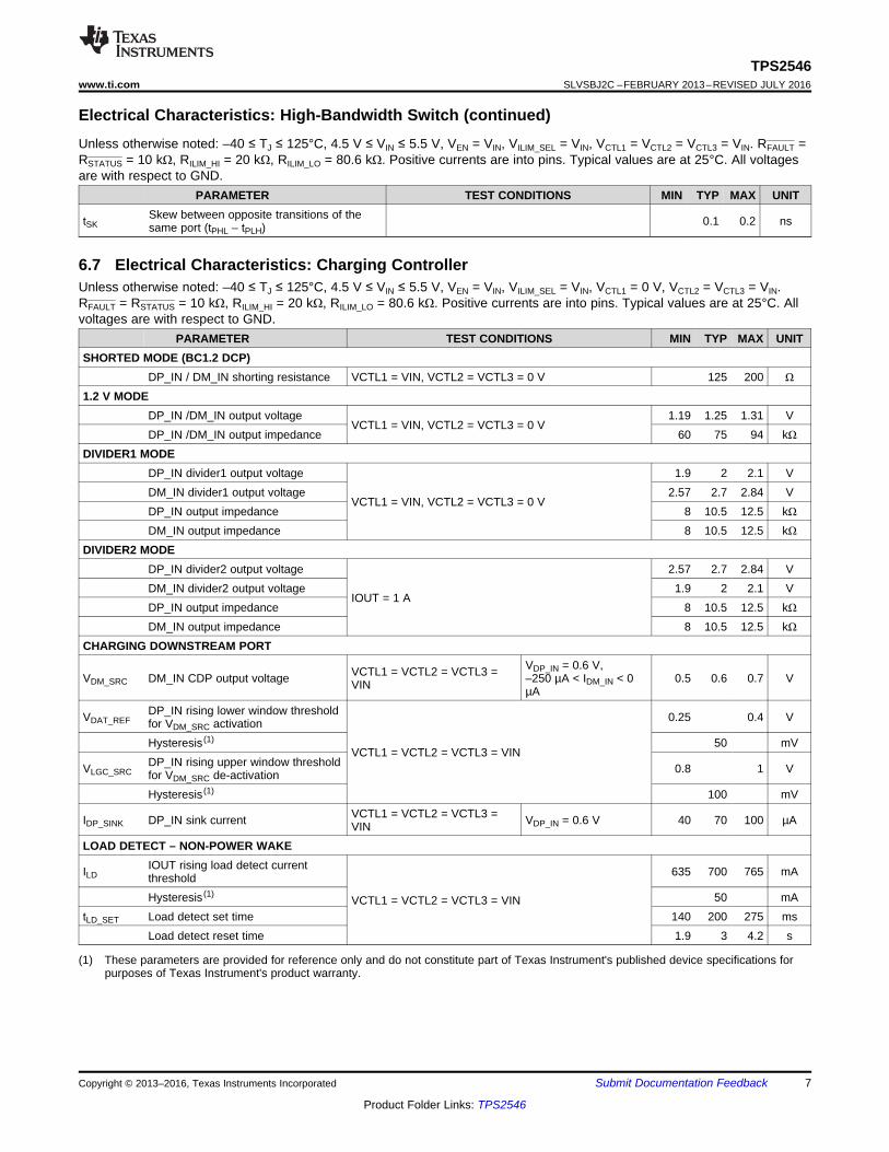
tSKSkew between opposite transitions of thesame port (tPHL – tPLH) 0.1 0.2 ns
(1) These parameters are provided for reference only and do not constitute part of Texas Instrument's published device specifications forpurposes of Texas Instrument's product warranty.
6.7 Electrical Characteristics: Charging ControllerUnless otherwise noted: –40 ≤ TJ ≤ 125°C, 4.5 V ≤ VIN ≤ 5.5 V, VEN = VIN, VILIM_SEL = VIN, VCTL1 = 0 V, VCTL2 = VCTL3 = VIN.RFAULT = RSTATUS = 10 kΩ, RILIM_HI = 20 kΩ, RILIM_LO = 80.6 kΩ. Positive currents are into pins. Typical values are at 25°C. Allvoltages are with respect to GND.
PARAMETER TEST CONDITIONS MIN TYP MAX UNITSHORTED MODE (BC1.2 DCP)
DP_IN / DM_IN shorting resistance VCTL1 = VIN, VCTL2 = VCTL3 = 0 V 125 200 Ω
1.2 V MODEDP_IN /DM_IN output voltage
VCTL1 = VIN, VCTL2 = VCTL3 = 0 V1.19 1.25 1.31 V
DP_IN /DM_IN output impedance 60 75 94 kΩDIVIDER1 MODE
DP_IN divider1 output voltage
VCTL1 = VIN, VCTL2 = VCTL3 = 0 V
1.9 2 2.1 VDM_IN divider1 output voltage 2.57 2.7 2.84 VDP_IN output impedance 8 10.5 12.5 kΩDM_IN output impedance 8 10.5 12.5 kΩ
DIVIDER2 MODEDP_IN divider2 output voltage
IOUT = 1 A
2.57 2.7 2.84 VDM_IN divider2 output voltage 1.9 2 2.1 VDP_IN output impedance 8 10.5 12.5 kΩDM_IN output impedance 8 10.5 12.5 kΩ
CHARGING DOWNSTREAM PORT
VDM_SRC DM_IN CDP output voltage VCTL1 = VCTL2 = VCTL3 =VIN
VDP_IN = 0.6 V,–250 µA < IDM_IN < 0µA
0.5 0.6 0.7 V
VDAT_REFDP_IN rising lower window thresholdfor VDM_SRC activation
VCTL1 = VCTL2 = VCTL3 = VIN
0.25 0.4 V
Hysteresis (1) 50 mV
VLGC_SRCDP_IN rising upper window thresholdfor VDM_SRC de-activation 0.8 1 V
Hysteresis (1) 100 mV
IDP_SINK DP_IN sink current VCTL1 = VCTL2 = VCTL3 =VIN VDP_IN = 0.6 V 40 70 100 µA
LOAD DETECT – NON-POWER WAKE
ILDIOUT rising load detect currentthreshold
VCTL1 = VCTL2 = VCTL3 = VIN
635 700 765 mA
Hysteresis (1) 50 mAtLD_SET Load detect set time 140 200 275 ms
Load detect reset time 1.9 3 4.2 s
8
TPS2546SLVSBJ2C –FEBRUARY 2013–REVISED JULY 2016 www.ti.com
Product Folder Links: TPS2546
Submit Documentation Feedback Copyright © 2013–2016, Texas Instruments Incorporated
Electrical Characteristics: Charging Controller (continued)Unless otherwise noted: –40 ≤ TJ ≤ 125°C, 4.5 V ≤ VIN ≤ 5.5 V, VEN = VIN, VILIM_SEL = VIN, VCTL1 = 0 V, VCTL2 = VCTL3 = VIN.RFAULT = RSTATUS = 10 kΩ, RILIM_HI = 20 kΩ, RILIM_LO = 80.6 kΩ. Positive currents are into pins. Typical values are at 25°C. Allvoltages are with respect to GND.
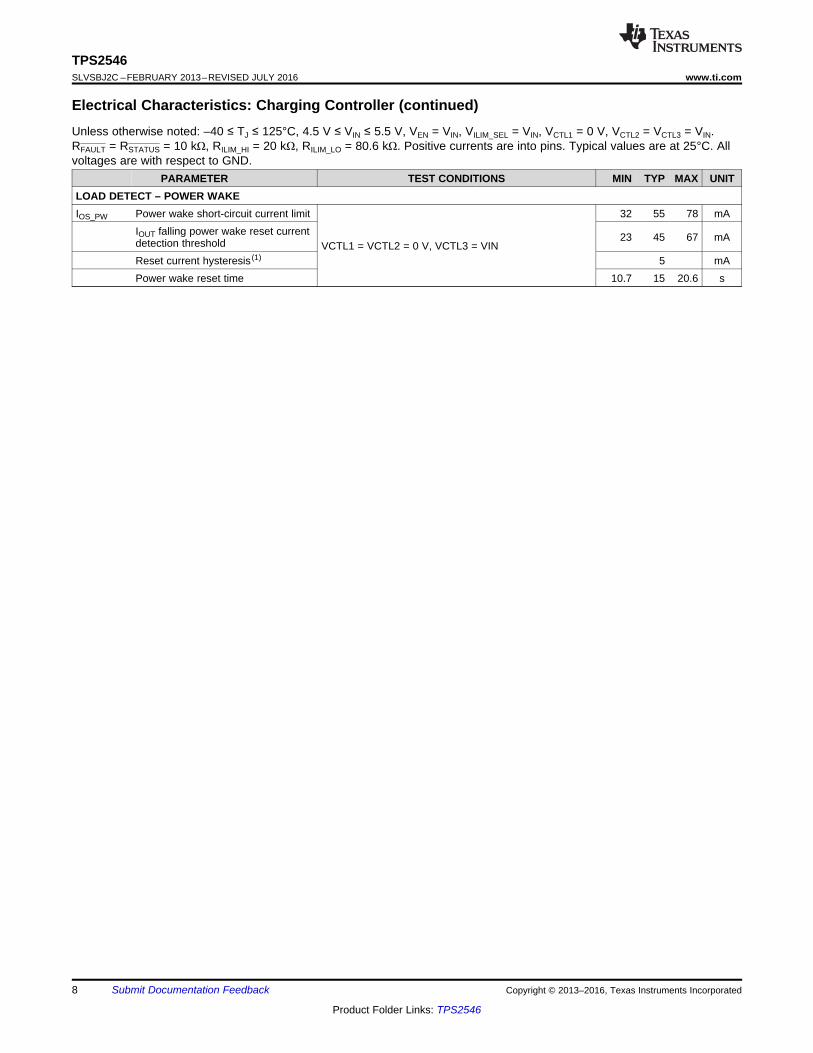
PARAMETER TEST CONDITIONS MIN TYP MAX UNITLOAD DETECT – POWER WAKEIOS_PW Power wake short-circuit current limit
VCTL1 = VCTL2 = 0 V, VCTL3 = VIN
32 55 78 mAIOUT falling power wake reset currentdetection threshold 23 45 67 mA
Reset current hysteresis (1) 5 mAPower wake reset time 10.7 15 20.6 s
0
0.2
0.4
0.6
0.8
1
1.2
−40 −20 0 20 40 60 80 100Junction Temperature (°C)
Dis
able
d IN
Sup
ply
Cur
rent
(µA
)
VIN = 5.5 V
G005
130
140
150
160
170
180
190
−40 −25 −10 5 20 35 50 65 80 95 110 125Junction Temperature (°C)
Ena
bled
IN S
uppl
y C
urre
nt (
µA)
VIN = 4.5 VVIN = 5 VVIN = 5.5 V
Device configured for SDPVILIMSEL = 0 V
G006
460
480
500
520
540
560
580
−40 −25 −10 5 20 35 50 65 80 95 110 125Junction Temperature (°C)
OU
T D
isch
arge
Res
ista
nce
(Ω)
VIN = 4.5 VVIN = 5 VVIN = 5.5 V
G003
0
500
1000
1500
2000
2500
3000
3500
−40 −25 −10 5 20 35 50 65 80 95 110 125Junction Temperature (°C)
OU
T S
hort
Circ
uit C
urre
nt L
imit
(mA
)
RILIM_LO = 210 kΩRILIM_LO = 80.6 kΩRILIM_HI = 20 kΩRILIM_HI = 16.9 kΩ
G004
50
60
70
80
90
100
−40 −25 −10 5 20 35 50 65 80 95 110 125Junction Temperature (°C)
On
Res
ista
nce
(mΩ
)
G001
0
0.05
0.1
0.15
0.2
0.25
0.3
−40 −25 −10 5 20 35 50 65 80 95 110 125Junction Temperature (°C)
Rev
erse
Lea
kage
Cur
rent
(µA
)
G002
9
TPS2546www.ti.com SLVSBJ2C –FEBRUARY 2013–REVISED JULY 2016
Product Folder Links: TPS2546
Submit Documentation FeedbackCopyright © 2013–2016, Texas Instruments Incorporated
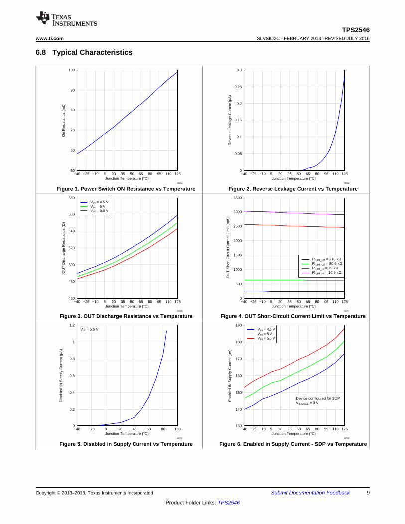
6.8 Typical Characteristics
Figure 1. Power Switch ON Resistance vs Temperature Figure 2. Reverse Leakage Current vs Temperature
Figure 3. OUT Discharge Resistance vs Temperature Figure 4. OUT Short-Circuit Current Limit vs Temperature
Figure 5. Disabled in Supply Current vs Temperature Figure 6. Enabled in Supply Current - SDP vs Temperature
0
60
OIR
R-
Off
Sta
teIs
ola
tio
n-
dB
10
40
20
50
0.01 1
Frequency - GHz
0.1 10
30
0
60
XT
AL
K-
ON
Sta
teC
ros
s-C
ha
nn
el
Iso
lati
on
-d
B
10
40
20
50
0.01 1
Frequency - GHz
0.1 10
30
80
70
-20
0
Tra
ns
mis
sio
nG
ain
-d
B
-20
-10
-15
-5
0.01 1
Frequency - GHz
0.1 100
100
200
300
400
500
600
700
0 1 2 3 4 5 6 7 8 9 10Sinking Current (mA)
Out
put L
ow V
olta
ge (
mV
)
TJ = −40°CTJ = 25°CTJ = 125°C
VIN = 4.5 V
G009
160
170
180
190
200
210
220
−40 −25 −10 5 20 35 50 65 80 95 110 125Junction Temperature (°C)
Ena
bled
IN S
uppl
y C
urre
nt (
µA)
VIN = 4.5 VVIN = 5 VVIN = 5.5 V
Device configured for CDP
G007
180
190
200
210
220
230
240
−40 −25 −10 5 20 35 50 65 80 95 110 125Junction Temperature (°C)
Ena
bled
IN S
uppl
y C
urre
nt (
µA)
VIN = 4.5 VVIN = 5 VVIN = 5.5 V
Device configured for DCP AUTO
G008
10
TPS2546SLVSBJ2C –FEBRUARY 2013–REVISED JULY 2016 www.ti.com
Product Folder Links: TPS2546
Submit Documentation Feedback Copyright © 2013–2016, Texas Instruments Incorporated
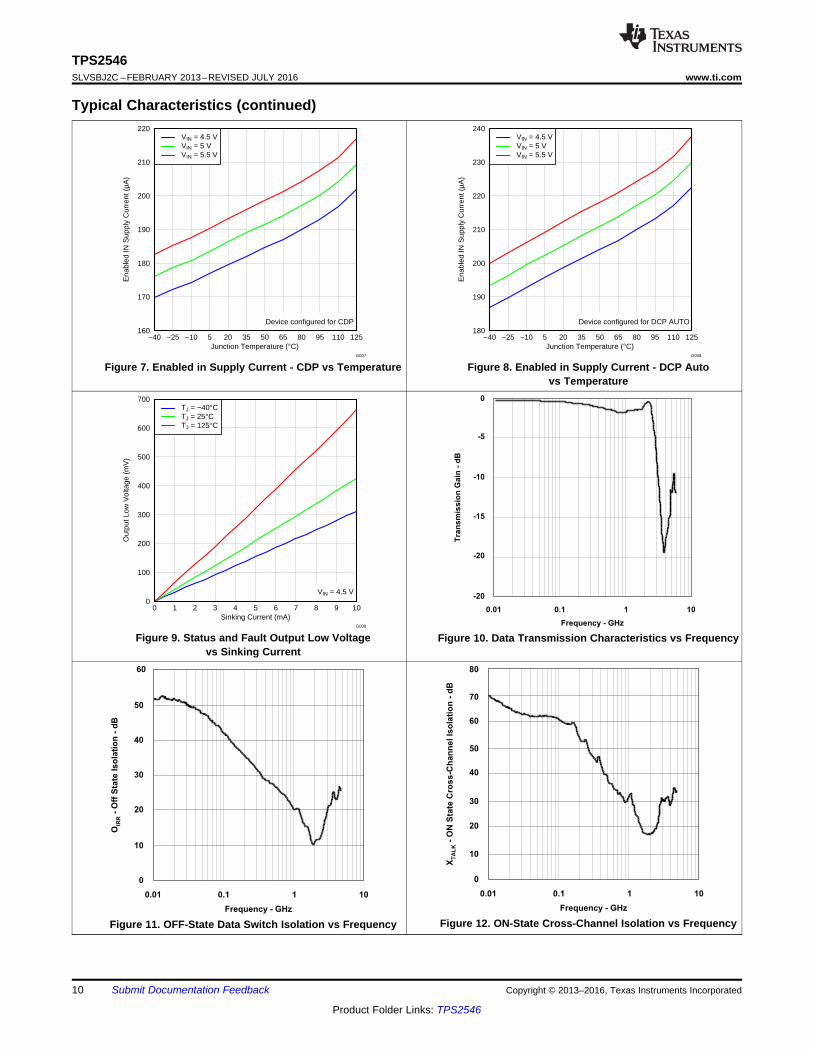
Typical Characteristics (continued)
Figure 7. Enabled in Supply Current - CDP vs Temperature Figure 8. Enabled in Supply Current - DCP Autovs Temperature
Figure 9. Status and Fault Output Low Voltagevs Sinking Current
Figure 10. Data Transmission Characteristics vs Frequency
Figure 11. OFF-State Data Switch Isolation vs Frequency Figure 12. ON-State Cross-Channel Isolation vs Frequency
I
500 mA/divIN
V
5 V/divEN
V
2 V/divOUT
t - Time - 1 ms/div
RLOAD = 5
C = 150 F
Ω
µLOAD
G021
52
53
54
55
56
57
58
59
−40 −25 −10 5 20 35 50 65 80 95 110 125Junction Temperature (°C)
Pow
er W
ake
Cur
rent
Lim
it (
mA
)
G017
600
620
640
660
680
700
720
740
−40 −25 −10 5 20 35 50 65 80 95 110 125Junction Temperature (°C)
Cur
rent
(m
A)
IOS - OUT Short Circuit Current LimitILD - IOUT Rising Load Detect Threshold
RILIM_LO = 80.6 kΩ
G015
200
205
210
215
220
225
230
−40 −25 −10 5 20 35 50 65 80 95 110 125Junction Temperature (°C)
Load
Det
ect S
et T
ime
(ms)
G016
G013
0.5
0.4
0.3
0.2
0.1
0
–0.1
–0.2
–0.3
–0.4
–0.5
0 0.2 0.4 0.6 0.8 1 1.2 1.4 1.6 1.8 2
Time (ns)
Diffe
ren
tia
l S
ign
al (V
)
G014
0.5
0.4
0.3
0.2
0.1
0
–0.1
–0.2
–0.3
–0.4
–0.5
0 0.2 0.4 0.6 0.8 1 1.2 1.4 1.6 1.8 2
Time (ns)
Diffe
ren
tia
l S
igna
l (V
)
11
TPS2546www.ti.com SLVSBJ2C –FEBRUARY 2013–REVISED JULY 2016
Product Folder Links: TPS2546
Submit Documentation FeedbackCopyright © 2013–2016, Texas Instruments Incorporated
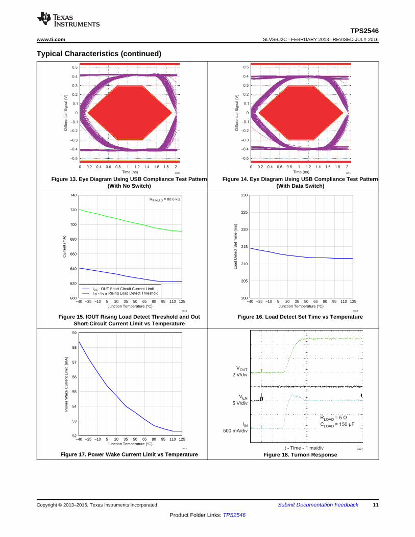
Typical Characteristics (continued)
Figure 13. Eye Diagram Using USB Compliance Test Pattern(With No Switch)
Figure 14. Eye Diagram Using USB Compliance Test Pattern(With Data Switch)
Figure 15. IOUT Rising Load Detect Threshold and OutShort-Circuit Current Limit vs Temperature
Figure 16. Load Detect Set Time vs Temperature
Figure 17. Power Wake Current Limit vs Temperature Figure 18. Turnon Response
I
1 A/divIN
V
5 V/divEN
V
5 V/div/FAULT
t - Time - 5 ms/div
RILM_HI = 20 kΩ
G024
I
2 A/divIN
V
2 V/divOUT
V
5 V/div/FAULT
t - Time - 2 ms/div
RILIM_HI
LOAD
LOAD
= 20 k
R = 5
C = 150 F
Ω
Ω
µ
G025
I
500 mA/divIN
V
5 V/divEN
V
2 V/divOUT
t - Time - 1 ms/div
RLOAD = 5
C = 150 F
Ω
µLOAD
G022
I
500 mA/divIN
V
5 V/divEN
V
5 V/div/FAULT
t - Time - 2 ms/div
RILM_LO = 80.6 kΩ
G023
12
TPS2546SLVSBJ2C –FEBRUARY 2013–REVISED JULY 2016 www.ti.com
Product Folder Links: TPS2546
Submit Documentation Feedback Copyright © 2013–2016, Texas Instruments Incorporated
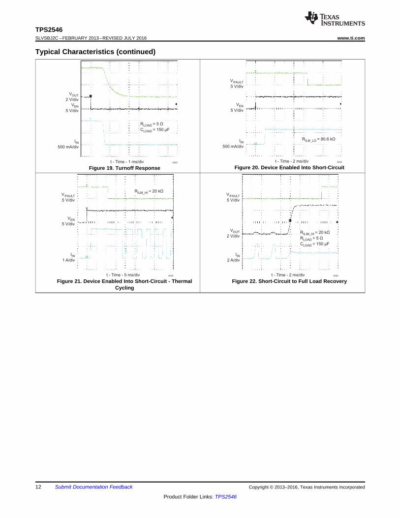
Typical Characteristics (continued)
Figure 19. Turnoff Response Figure 20. Device Enabled Into Short-Circuit
Figure 21. Device Enabled Into Short-Circuit - ThermalCycling
Figure 22. Short-Circuit to Full Load Recovery
tIOS
IOUT
IOS
5 V
VOUT
0 V
tDCHG
VEN
VOUT
ton
50 % 50 %
toff
90 %
10 %
10%
90%
VOUT
tr
tf
OUT
RL
CL
13
TPS2546www.ti.com SLVSBJ2C –FEBRUARY 2013–REVISED JULY 2016
Product Folder Links: TPS2546
Submit Documentation FeedbackCopyright © 2013–2016, Texas Instruments Incorporated
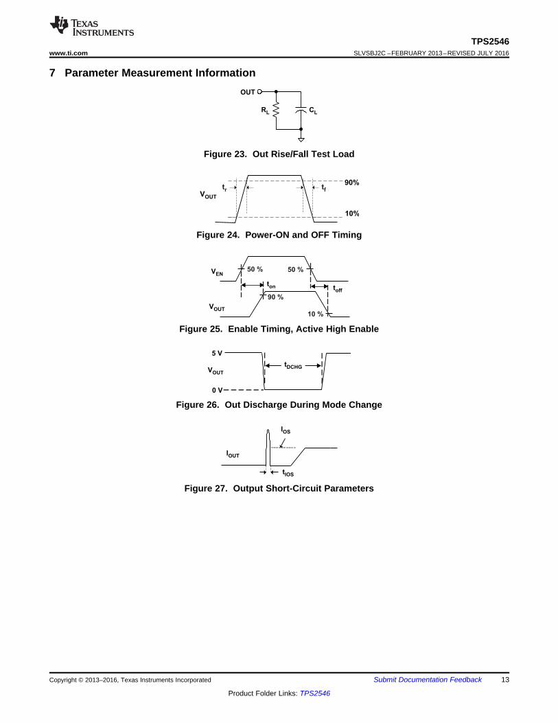
7 Parameter Measurement Information
Figure 23. Out Rise/Fall Test Load
Figure 24. Power-ON and OFF Timing
Figure 25. Enable Timing, Active High Enable
Figure 26. Out Discharge During Mode Change
Figure 27. Output Short-Circuit Parameters
14
TPS2546SLVSBJ2C –FEBRUARY 2013–REVISED JULY 2016 www.ti.com
Product Folder Links: TPS2546
Submit Documentation Feedback Copyright © 2013–2016, Texas Instruments Incorporated
8 Detailed Description
8.1 OverviewThe following overview references various industry standards. TI recommends consulting the most up-to-datestandard to ensure the most recent and accurate information. Rechargeable portable equipment requires anexternal power source to charge its batteries. USB ports are a convenient location for charging, because of anavailable 5-V power source. Universally accepted standards are required to make sure host and client-sidedevices operate together in a system to ensure power management requirements are met. Traditionally, hostports following the USB 2.0 specification must provide at least 500 mA to downstream client-side devices.Because multiple USB devices can attach to a single USB port through a bus-powered hub, it is the responsibilityof the client-side device to negotiate its power allotment from the host, ensuring the total current draw does notexceed 500 mA. In general, each USB device is granted 100 mA, and may request more current in 100-mA unitsteps up to 500 mA. The host may grant or deny based on the available current. A USB 3.0 host port not onlyprovides higher data rate than USB 2.0 port, but also raises the unit load from 100 mA to 150 mA. It is alsorequired to provide a minimum current of 900 mA to downstream client-side devices.
Additionally, the success of USB makes the mini-USB connector a popular choice for wall adapter cables. Thisallows a portable device to charge from both a wall adapter, and USB port with only one connector. As USBcharging has gained popularity, the 500-mA minimum defined by USB 2.0 or 900 mA for USB 3.0 has becomeinsufficient for many handset and personal media players, which need a higher charging rate. Wall adapters canprovide much more current than 500 mA/900 mA. Several new standards have been introduced, definingprotocol handshaking methods that allow host and client devices to acknowledge and draw additional currentbeyond the 500 mA/900 mA minimum defined by USB 2.0 and 3.0, while still using a single micro-USB inputconnector.
The TPS2546 supports four of the most common USB charging schemes found in popular handheld media andcellular devices:• USB Battery Charging Specification BC1.2• Chinese Telecommunications Industry Standard YD/T 1591-2009• Divider Mode• 1.2-V Mode
YD/T 1591-2009 is a subset of BC1.2 specifications supported by vast majority of devices that implement USBchanging. Divider and 1.2-V charging schemes are supported in devices from specific, yet popular devicemakers.
BC1.2 lists three different port types:• Standard Downstream Port (SDP)• Charging Downstream Port (CDP)• Dedicated Charging Port (DCP)
BC1.2 defines a charging port as a downstream facing USB port that provides power for charging portableequipment. Under this definition, CDP and DCP are defined as charging ports.
Disable + UVLO+Discharge
Driver
CS
CurrentLimit
ChargePump
UVLOThermalSense
8-ms Deglitch
OTSD
CurrentSense
IN
EN
ILIM_HI
CTL1
DP_IN
DM_IN
OUT
GND
FAULT
8-ms Deglitch(falling edge)
Current Limitselect
ILIM_LO
ILIM_SEL
STATUS
TPS2543
Only
DP_OUT
DM_OUT
CTL2
CTL3
Logic
control
CDP
Detection
DCPDetection Auto-Detection
Divider
Mode
ILIM_SEL
Discharge
discharge
LD cur set
LD cur set
Discharge
OC
OC
Copyright © 2016, Texas Instruments Incorporated
15
TPS2546www.ti.com SLVSBJ2C –FEBRUARY 2013–REVISED JULY 2016
Product Folder Links: TPS2546
Submit Documentation FeedbackCopyright © 2013–2016, Texas Instruments Incorporated
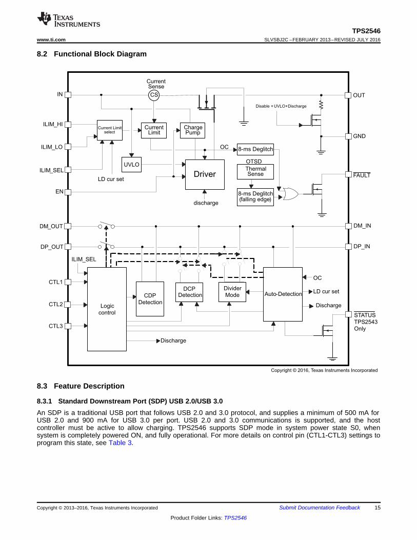
8.2 Functional Block Diagram
8.3 Feature Description
8.3.1 Standard Downstream Port (SDP) USB 2.0/USB 3.0An SDP is a traditional USB port that follows USB 2.0 and 3.0 protocol, and supplies a minimum of 500 mA forUSB 2.0 and 900 mA for USB 3.0 per port. USB 2.0 and 3.0 communications is supported, and the hostcontroller must be active to allow charging. TPS2546 supports SDP mode in system power state S0, whensystem is completely powered ON, and fully operational. For more details on control pin (CTL1-CTL3) settings toprogram this state, see Table 3.
AutoDetect
CDPDetect
2.0 V
2.7 V
US
B
Con
nect
or
D-
D+
VBUS
GND
D- Out
D+ Out
US
B H
ost/H
ub
1.2 V
< 2
00
TPS2546
Copyright © 2016, Texas Instruments Incorporated
16
TPS2546SLVSBJ2C –FEBRUARY 2013–REVISED JULY 2016 www.ti.com
Product Folder Links: TPS2546
Submit Documentation Feedback Copyright © 2013–2016, Texas Instruments Incorporated
Feature Description (continued)8.3.2 Charging Downstream Port (CDP)A CDP is a USB port that follows USB BC1.2 and supplies a minimum of 1.5 A per port. It provides power andmeets USB 2.0 requirements for device enumeration. USB 2.0 communications is supported, and the hostcontroller must be active to allow charging. What separates a CDP from an SDP is the host-charge handshakinglogic that identifies this port as a CDP. A CDP is identifiable by a compliant BC1.2 client device, and allows foradditional current draw by the client device.
The CDP process is done in two steps. During step one, the portable equipment outputs a nominal 0.6-V outputon the D+ line, and reads the voltage input on the D– line. The portable device detects it is connected to an SDPif the voltage is less than the nominal data detect voltage of 0.3 V. The portable device detects that it isconnected to a Charging Port if the D– voltage is greater than the nominal data detect voltage of 0.3 V, andoptionally less than 0.8 V.
The second step is necessary for portable equipment to determine if it is connected to CDP or DCP. Theportable device outputs a nominal 0.6 V output on its D– line, and reads the voltage input on its D+ line. Theportable device detects it is connected to a CDP if the data line being read remains less than the nominal datadetect voltage of 0.3 V. The portable device detects it is connected to a DCP if the data line being read is greaterthan the nominal data detect voltage of 0.3 V.
TPS2546 supports CDP mode in system power state S0 when system is completely powered ON, and fullyoperational. For more details on control pin (CTL1-CTL3) settings to program this state, see Table 3.
8.3.3 Dedicated Charging Port (DCP)A DCP only provides power but does not support data connection to an upstream port. As shown in followingsections, a DCP is identified by the electrical characteristics of the data lines. The TPS2546 emulates DCP intwo charging states, namely DCP Forced and DCP Auto as shown in Figure 37. In DCP Forced state the devicesupports one of the two DCP charging schemes, namely Divider1 or Shorted. In the DCP Auto state, the devicecharge detection state machine is activated to selectively implement charging schemes involved with theShorted, Divider1, Divider2, and 1.2-V modes. Shorted DCP mode complies with BC1.2 and ChineseTelecommunications Industry Standard YD/T 1591-2009, while the Divider and 1.2-V modes are employed tocharge devices that do not comply with BC1.2 DCP standard.
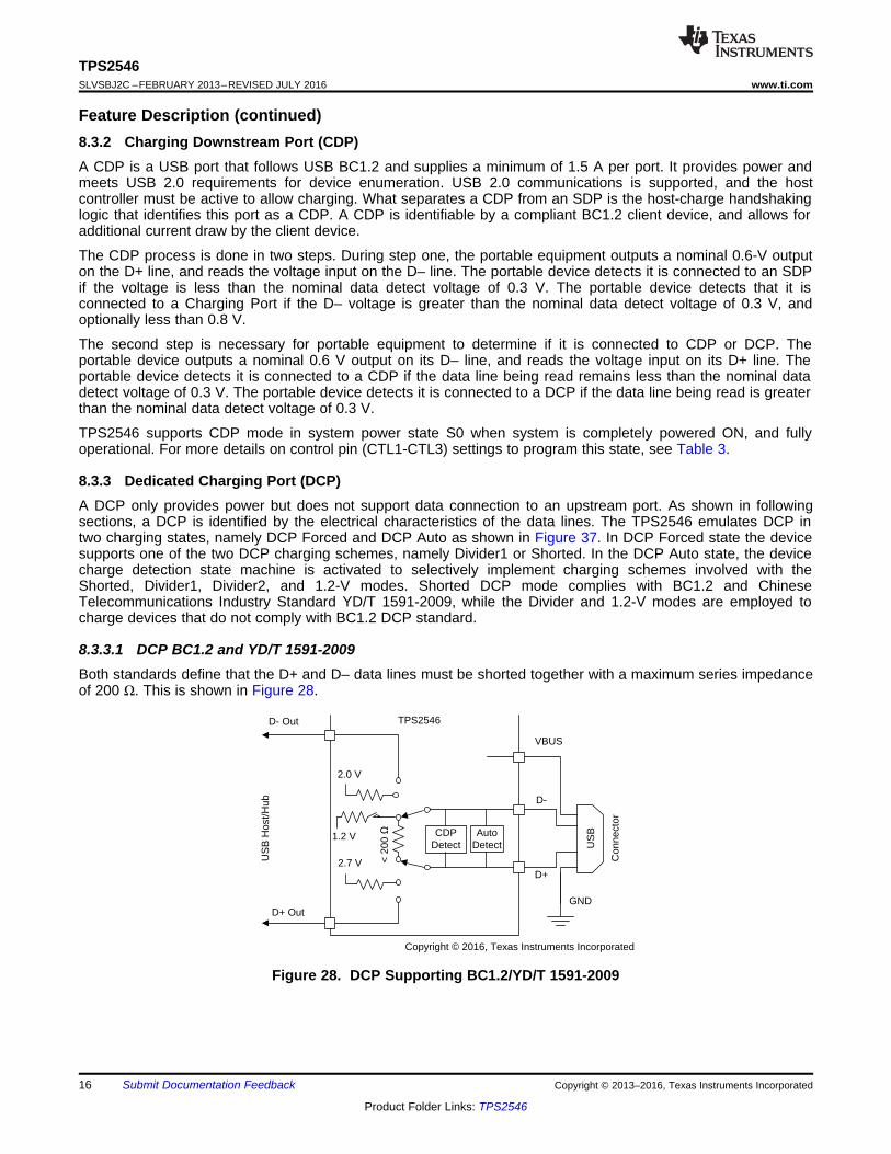
8.3.3.1 DCP BC1.2 and YD/T 1591-2009Both standards define that the D+ and D– data lines must be shorted together with a maximum series impedanceof 200 Ω. This is shown in Figure 28.
Figure 28. DCP Supporting BC1.2/YD/T 1591-2009
AutoDetect
CDPDetect
2.0 V
2.7 V
US
B
Con
nect
orD-
D+
VBUS
GND
D- Out
D+ Out
US
B H
ost/H
ub
1.2 V
< 2
00
TPS2546
Copyright © 2016, Texas Instruments Incorporated
AutoDetect
CDPDetect
2.7 V
2.0 V
US
B
Con
nect
or
D-
D+
VBUS
GND
D- Out
D+ Out
US
B H
ost/H
ub
1.2 V
< 2
00
TPS2546
Copyright © 2016, Texas Instruments Incorporated
17
TPS2546www.ti.com SLVSBJ2C –FEBRUARY 2013–REVISED JULY 2016
Product Folder Links: TPS2546
Submit Documentation FeedbackCopyright © 2013–2016, Texas Instruments Incorporated
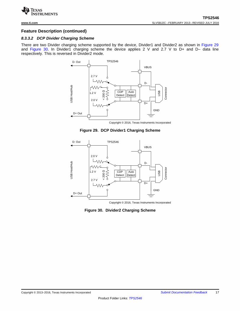
Feature Description (continued)8.3.3.2 DCP Divider Charging SchemeThere are two Divider charging scheme supported by the device, Divider1 and Divider2 as shown in Figure 29and Figure 30. In Divider1 charging scheme the device applies 2 V and 2.7 V to D+ and D– data linerespectively. This is reversed in Divider2 mode.
Figure 29. DCP Divider1 Charging Scheme
Figure 30. Divider2 Charging Scheme
AutoDetect
CDPDetect
2.0 V
2.7 V
US
B
Con
nect
or
D-
D+
VBUS
GND
D- Out
D+ Out
US
B H
ost/H
ub
1.2 V
< 2
00
TPS2546
Copyright © 2016, Texas Instruments Incorporated
18
TPS2546SLVSBJ2C –FEBRUARY 2013–REVISED JULY 2016 www.ti.com
Product Folder Links: TPS2546
Submit Documentation Feedback Copyright © 2013–2016, Texas Instruments Incorporated
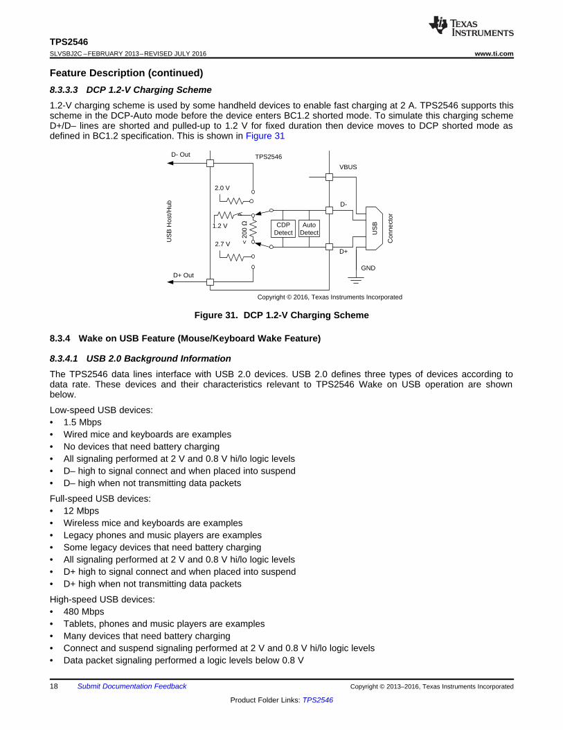
Feature Description (continued)8.3.3.3 DCP 1.2-V Charging Scheme1.2-V charging scheme is used by some handheld devices to enable fast charging at 2 A. TPS2546 supports thisscheme in the DCP-Auto mode before the device enters BC1.2 shorted mode. To simulate this charging schemeD+/D– lines are shorted and pulled-up to 1.2 V for fixed duration then device moves to DCP shorted mode asdefined in BC1.2 specification. This is shown in Figure 31
Figure 31. DCP 1.2-V Charging Scheme
8.3.4 Wake on USB Feature (Mouse/Keyboard Wake Feature)
8.3.4.1 USB 2.0 Background InformationThe TPS2546 data lines interface with USB 2.0 devices. USB 2.0 defines three types of devices according todata rate. These devices and their characteristics relevant to TPS2546 Wake on USB operation are shownbelow.
Low-speed USB devices:• 1.5 Mbps• Wired mice and keyboards are examples• No devices that need battery charging• All signaling performed at 2 V and 0.8 V hi/lo logic levels• D– high to signal connect and when placed into suspend• D– high when not transmitting data packets
Full-speed USB devices:• 12 Mbps• Wireless mice and keyboards are examples• Legacy phones and music players are examples• Some legacy devices that need battery charging• All signaling performed at 2 V and 0.8 V hi/lo logic levels• D+ high to signal connect and when placed into suspend• D+ high when not transmitting data packets
High-speed USB devices:• 480 Mbps• Tablets, phones and music players are examples• Many devices that need battery charging• Connect and suspend signaling performed at 2 V and 0.8 V hi/lo logic levels• Data packet signaling performed a logic levels below 0.8 V
19
TPS2546www.ti.com SLVSBJ2C –FEBRUARY 2013–REVISED JULY 2016
Product Folder Links: TPS2546
Submit Documentation FeedbackCopyright © 2013–2016, Texas Instruments Incorporated
Feature Description (continued)• D+ high to signal connect and when placed into suspend (same as a full-speed device)• D+ and D– low when not transmitting data packets
8.3.4.2 Wake On USBWake on USB is the ability of a wake configured USB device to wake a computer system from its S3 sleep stateback to its S0 working state. Wake on USB requires the data lines to be connected to the system USB hostbefore the system is placed into its S3 sleep state, and remain continuously connected until they are used towake the system.
The TPS2546 supports low-speed and high-speed HID (human interface device like mouse/key board) wakefunction. There are two scenarios under which wake on mouse are supported by the TPS2546. The specific CTLpin changes that the TPS2546 overrides are shown below. The information is presented as CTL1, CTL2, CTL3.The ILIM_SEL pin plays no role1. 111 (CDP/SDP2) to 011 (DCP-Auto)2. 010 (SDP1) to 011 (DCP-Auto)
NOTEThe 110 (SDP1) to 011 (DCP-Auto) transition is not supported. This is done for practicalreasons, because the transition involves changes to two CTL pins. Depending on whichCTL pin changes first, the device sees either a temporary 111 or 010 command. The 010command is safe but the 111 command causes an OUT discharge as the TPS2546instead proceeds to the 111 state.
8.3.4.3 USB Slow-Speed and Full-Speed Device RecognitionTPS2546 is capable of detecting LS or FS device attachment when TPS2546 is in SDP or CDP mode. Per USBspecification, when no device is attached, the D+ and D– lines are near ground level. When a low-speedcompliant device is attached to the TPS2546 charging port, D– line is pulled high in its idle state(mouse/keyboard not activated). However, when a FS device is attached then the opposite is true in its idle state,that is, D+ is pulled high and D– remains at ground level.
TPS2546 monitors both D+ and D– lines while CTL pin settings are in CDP or SDP mode to detect LS or FS HIDdevice attachment. To support HID sleep wake, TPS2546 must first determine that it is attached to a LS or FSdevice when system is in S0 power state. TPS2546 does this as described above. While supporting a LS HIDwake is straight forward, supporting FS HID requires making a distinction between a FS and a HS device. This isbecause a high-speed device always presents itself initially as a full speed device (by a 1.5-K pullup resistor onD+). The negotiation for high speed then makes the distinction whereby the 1.5-K pullup resistor gets removed.
TPS2546 handles the distinction between a FS and HS device at connect by memorizing if the D+ line goes lowafter connect. A HS device after connect always undergoes negotiation for HS, which requires the 1.5-kΩ resistorpullup on D+ to be removed. To memorize a FS device, TPS2546 requires the device to remain connected for atleast 60 seconds while the system is in S0 mode, before placing it in sleep or S3 mode.
NOTEIf system is placed in sleep mode earlier than the 60 second window, a FS device may notget recognized and hence could fail to wake system from S3. This requirement does notapply for LS device.
8.3.4.3.1 No CTL Pin Timing Requirement After Wake Event and Transition from S3 to S0
Unlike the TPS2543, there is no CTL pin timing requirement for the TPS2546 when the wake configured USBdevice wakes the system from S3 back to S0. The TPS2543 requires the CTL pins to transition from the DCP-Auto setting back to the SDP/CDP setting within 64 ms of the attached USB device signaling a wake event (forexample, mouse clicked or keyboard key pressed). No such timing condition exists for the TPS2546.
20
TPS2546SLVSBJ2C –FEBRUARY 2013–REVISED JULY 2016 www.ti.com
Product Folder Links: TPS2546
Submit Documentation Feedback Copyright © 2013–2016, Texas Instruments Incorporated
Feature Description (continued)8.3.5 Load DetectTPS2546 offers system designers unique power management strategy not available in the industry from similardevices. There are two power management schemes supported by the TPS2546 through the STATUS pin, theyare:• Power Wake (PW)• Port Power Management (PPM)
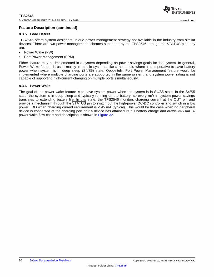
Either feature may be implemented in a system depending on power savings goals for the system. In general,Power Wake feature is used mainly in mobile systems, like a notebook, where it is imperative to save batterypower when system is in deep sleep (S4/S5) state. Oppositely, Port Power Management feature would beimplemented where multiple charging ports are supported in the same system, and system power rating is notcapable of supporting high-current charging on multiple ports simultaneously.
8.3.6 Power WakeThe goal of the power wake feature is to save system power when the system is in S4/S5 state. In the S4/S5state, the system is in deep sleep and typically running off the battery; so every mW in system power savingstranslates to extending battery life. In this state, the TPS2546 monitors charging current at the OUT pin andprovide a mechanism through the STATUS pin to switch out the high-power DC-DC controller and switch in a lowpower LDO when charging current requirement is < 45 mA (typical). This would be the case when no peripheraldevice is connected at the charging port or if a device has attained its full battery charge and draws <45 mA. Apower wake flow chart and description is shown in Figure 32.
Power Wake De-asserted /STATUS = 1
Current Limit = 55 mA
Power Wake Asserted /STATUS = 0
Current Limit = ILIM_HI setting
Load Current > 55 mA
OUT DischargePower Wake Asserted
/STATUS = 0Current Limit = 55 mA
Case 2A&2BNO LOAD DETECTED
Case 1LOAD DETECTED
OUT DISCHARGE
Load
Cur
rent
< 4
5 m
A
for
15s
Load being Chargedx TPS2546 is asserting power wakex System power is at its full capability x Load can charge at high currentx TPS2546 monitors port to detect when charging load is
done charging or removed
Charging Load Not Detected.x TPS2546 is not asserting power wake. System power is in
a low power state to save energy. x TPS2546 monitors port to detect when charging load is
attached and tries to charge
Charging Load Detectedx TPS2546 is asserting power wakex System power turns on to its full power statex Load Vbus is held low for 2 s to give the
power system time to turn on before the load tries to pull charging current again
Dis
char
ge =
tDS
CH
G_L
CHARGING
NOTCHARGING
Charging Current Detected
Copyright © 2016, Texas Instruments Incorporated
21
TPS2546www.ti.com SLVSBJ2C –FEBRUARY 2013–REVISED JULY 2016
Product Folder Links: TPS2546
Submit Documentation FeedbackCopyright © 2013–2016, Texas Instruments Incorporated
Feature Description (continued)
Figure 32. Power Wake Flow Chart
IN
OUT
EN
19 V
EN
DPDM
OC
POWER Block
USB Host Controller
I/O_EN
I/O_Sx
DM_OUTDP_OUTFAULTENCTL1CTL2CTL3
STATUS
ILIM_SEL
Switches Power between LDO and DC/DC based on
/STATUS
ILIM
_LO
ILIM
_HI
DM_INDP_INGND
VBUSD-D+GND
USB Receptacle
0011
ilimit set byRlim_Hi
LO
TPS2546
PeripheralDevice
CHARGING
Connected
LDO Disconnected/Shut-DownDC-DC Switched-In
EmbeddedController
4
5 V_DC/DC
5V_LDO
Copyright © 2016, Texas Instruments Incorporated
22
TPS2546SLVSBJ2C –FEBRUARY 2013–REVISED JULY 2016 www.ti.com
Product Folder Links: TPS2546
Submit Documentation Feedback Copyright © 2013–2016, Texas Instruments Incorporated
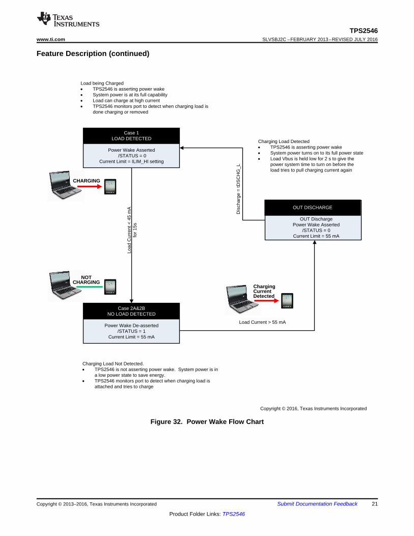
Feature Description (continued)8.3.6.1 Implementing Power Wake in Notebook SystemAn implementation of power wake in notebook platforms with the TPS2546 is shown in Figure 33 to Figure 35.Power wake function is used to select between a high-power DC-DC converter, and low-power LDO (100 mA)based on charging requirements. System power saving is achieved when under no charging conditions (theconnected device is fully charged or no device is connected) the DC-DC converter is turned off (to save powerbecause it is less efficient in low-power operating region) and the low-power LDO supplies standby power to thecharging port.
Power wake is activated in S4/S5 mode (0011 setting, see Table 3), TPS2546 is charging connected device asshown in Figure 33, STATUS is pulled LO (Case 1) which switches-out the LDO and switches-in the DC-DCconverter to handle high-current charging.
Figure 33. Case 1: System in S4/S5, Device Charging
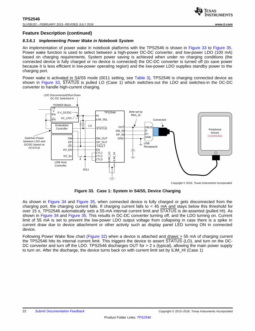
As shown in Figure 34 and Figure 35, when connected device is fully charged or gets disconnected from thecharging port, the charging current falls. If charging current falls to < 45 mA and stays below this threshold forover 15 s, TPS2546 automatically sets a 55-mA internal current limit and STATUS is de-asserted (pulled HI). Asshown in Figure 34 and Figure 35. This results in DC-DC converter turning off, and the LDO turning on. Currentlimit of 55 mA is set to prevent the low-power LDO output voltage from collapsing in case there is a spike incurrent draw due to device attachment or other activity such as display panel LED turning ON in connecteddevice.
Following Power Wake flow chart (Figure 32) when a device is attached and draws > 55 mA of charging currentthe TPS2546 hits its internal current limit. This triggers the device to assert STATUS (LO), and turn on the DC-DC converter and turn off the LDO. TPS2546 discharges OUT for > 2 s (typical), allowing the main power supplyto turn on. After the discharge, the device turns back on with current limit set by ILIM_HI (Case 1)
IN
OUT
EN
19 V
EN
DPDM
OC
POWER Block
USB Host Controller
I/O_EN
I/O_Sx
DM_OUTDP_OUTFAULTENCTL1CTL2CTL3
STATUS
ILIM_SEL
Switches Power between LDO and DC/DC based on
/STATUS
ILIM
_LO
ILIM
_HI
DM_INDP_INGND
VBUSD-D+GND
USB Receptacle
0011
Charging current falls to <45 mA and stays <45 mA for 15 sec, ilimit set to 55 mA
LOà HI
TPS2546
PeripheralDevice is
CHARGED!
Connected
EmbeddedController
4
DC-DC Disconnected/Shut-DownLDO Switched-In
Turns HI after 15 s
5V_DC/DC
5V_LDO
Copyright © 2016, Texas Instruments Incorporated
IN
OUT
5V_DC/DC
5V_LDO
EN
19 V
EN
DP
DM
OC
POWER Block
USB Host Controller
I/O_EN
I/O_Sx
DM_OUT
DP_OUT
FAULT
ENCTL1CTL2CTL3
STATUS
ILIM_SEL
Switches Power between LDO and DC/DC based on
/STATUS
ILIM
_LO
ILIM
_HI
DM_IN
DP_IN
GND
VBUSD-D+GND
USB Receptacle
0011
LO à HI
TPS2546
PeripheralDevice
DC-DC Disconnected/Shut-DownLDO Switched-In
EmbeddedController
4
Turns HI after 15 s
Charging current falls to <45 mA and stays <45 mA for 15 sec, ilimit set to 55 mA
NotConnected
Copyright © 2016, Texas Instruments Incorporated
23
TPS2546www.ti.com SLVSBJ2C –FEBRUARY 2013–REVISED JULY 2016
Product Folder Links: TPS2546
Submit Documentation FeedbackCopyright © 2013–2016, Texas Instruments Incorporated
Feature Description (continued)
Figure 34. Case 2A: System in S4/S5, No Device Attached
Figure 35. Case 2B: System in S4/S5, Attached Device Fully Charged
24
TPS2546SLVSBJ2C –FEBRUARY 2013–REVISED JULY 2016 www.ti.com
Product Folder Links: TPS2546
Submit Documentation Feedback Copyright © 2013–2016, Texas Instruments Incorporated
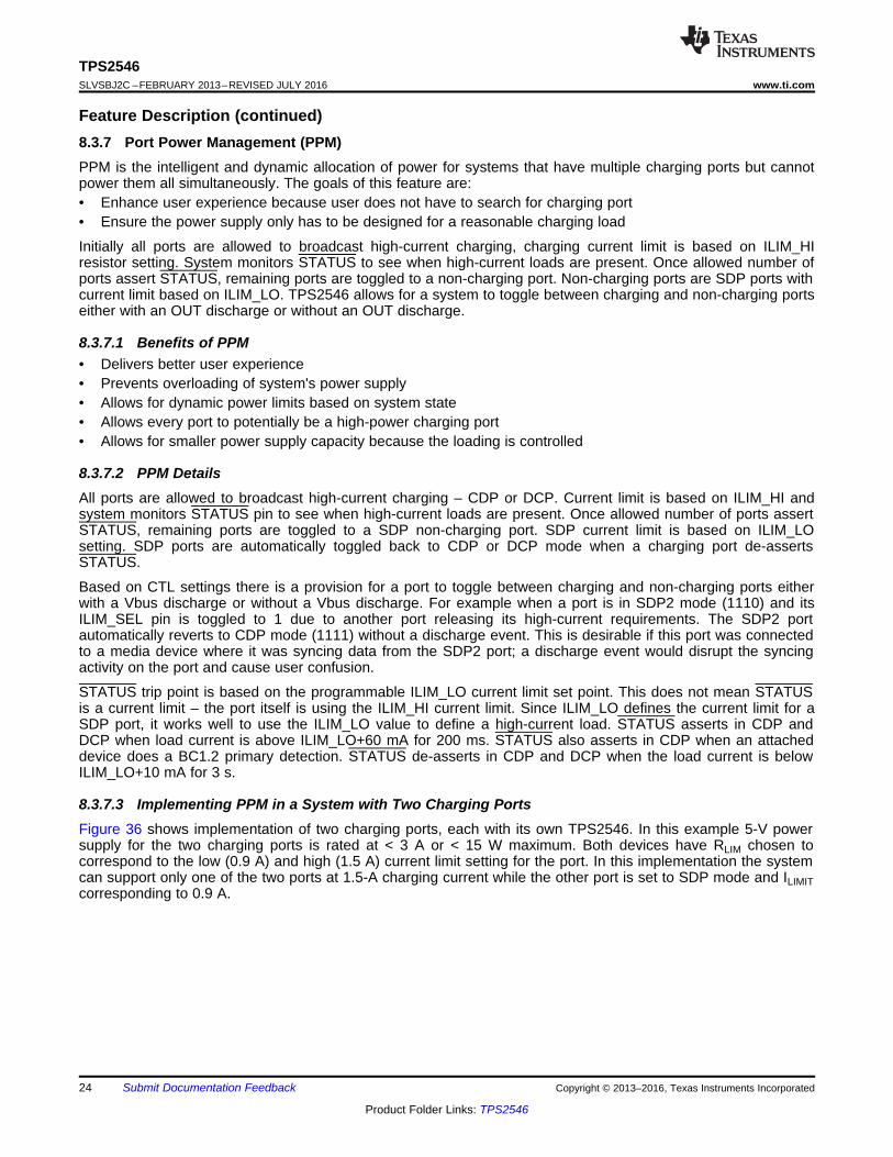
Feature Description (continued)8.3.7 Port Power Management (PPM)PPM is the intelligent and dynamic allocation of power for systems that have multiple charging ports but cannotpower them all simultaneously. The goals of this feature are:• Enhance user experience because user does not have to search for charging port• Ensure the power supply only has to be designed for a reasonable charging load
Initially all ports are allowed to broadcast high-current charging, charging current limit is based on ILIM_HIresistor setting. System monitors STATUS to see when high-current loads are present. Once allowed number ofports assert STATUS, remaining ports are toggled to a non-charging port. Non-charging ports are SDP ports withcurrent limit based on ILIM_LO. TPS2546 allows for a system to toggle between charging and non-charging portseither with an OUT discharge or without an OUT discharge.
8.3.7.1 Benefits of PPM• Delivers better user experience• Prevents overloading of system's power supply• Allows for dynamic power limits based on system state• Allows every port to potentially be a high-power charging port• Allows for smaller power supply capacity because the loading is controlled
8.3.7.2 PPM DetailsAll ports are allowed to broadcast high-current charging – CDP or DCP. Current limit is based on ILIM_HI andsystem monitors STATUS pin to see when high-current loads are present. Once allowed number of ports assertSTATUS, remaining ports are toggled to a SDP non-charging port. SDP current limit is based on ILIM_LOsetting. SDP ports are automatically toggled back to CDP or DCP mode when a charging port de-assertsSTATUS.
Based on CTL settings there is a provision for a port to toggle between charging and non-charging ports eitherwith a Vbus discharge or without a Vbus discharge. For example when a port is in SDP2 mode (1110) and itsILIM_SEL pin is toggled to 1 due to another port releasing its high-current requirements. The SDP2 portautomatically reverts to CDP mode (1111) without a discharge event. This is desirable if this port was connectedto a media device where it was syncing data from the SDP2 port; a discharge event would disrupt the syncingactivity on the port and cause user confusion.
STATUS trip point is based on the programmable ILIM_LO current limit set point. This does not mean STATUSis a current limit – the port itself is using the ILIM_HI current limit. Since ILIM_LO defines the current limit for aSDP port, it works well to use the ILIM_LO value to define a high-current load. STATUS asserts in CDP andDCP when load current is above ILIM_LO+60 mA for 200 ms. STATUS also asserts in CDP when an attacheddevice does a BC1.2 primary detection. STATUS de-asserts in CDP and DCP when the load current is belowILIM_LO+10 mA for 3 s.
8.3.7.3 Implementing PPM in a System with Two Charging PortsFigure 36 shows implementation of two charging ports, each with its own TPS2546. In this example 5-V powersupply for the two charging ports is rated at < 3 A or < 15 W maximum. Both devices have RLIM chosen tocorrespond to the low (0.9 A) and high (1.5 A) current limit setting for the port. In this implementation the systemcan support only one of the two ports at 1.5-A charging current while the other port is set to SDP mode and ILIMITcorresponding to 0.9 A.
48.7 K(0.9 A)
29.8 K(1.5 A)
IN
EN
FAULT
STATUS
CTL3CTL2CTL1ILIM_SEL
ILIM_LOILIM_HI
OUTDM_INDP_IN
USB ChargingPort #1
GND
48.7 K(0.9 A)
29.8 K(1.5 A)
IN
EN
FAULT
STATUS
CTL3CTL2CTL1ILIM_SEL
ILIM_LOILIM_HI
OUT
DM_INDP_IN
USB ChargingPort #2
GND
100 K
100 K
5V
EN_1FAULT_1
S0_S3
5 V
EN_2FAULT_2
TPS2546 Port 1
TPS2546 Port 2
Copyright © 2016, Texas Instruments Incorporated
25
TPS2546www.ti.com SLVSBJ2C –FEBRUARY 2013–REVISED JULY 2016
Product Folder Links: TPS2546
Submit Documentation FeedbackCopyright © 2013–2016, Texas Instruments Incorporated
Feature Description (continued)
Figure 36. Implementing Port Power Management in a System Supporting Two Charging Ports
8.3.8 Overcurrent ProtectionWhen an overcurrent condition is detected, the device maintains a constant output current and reduces theoutput voltage accordingly. Two possible overload conditions can occur. In the first condition, the output hasbeen shorted before the device is enabled or before VIN has been applied. The TPS2546 senses the short andimmediately switches into a constant-current output. In the second condition, a short or an overload occurs whilethe device is enabled. At the instant the overload occurs, high currents may flow for nominally one to twomicroseconds before the current-limit circuit can react. The device operates in constant-current mode after thecurrent-limit circuit has responded. Complete shutdown occurs only if the fault is present long enough to activatethermal limiting. The device remains off until the junction temperature cools approximately 20°C and then re-starts. The device continues to cycle on/off until the overcurrent condition is removed.
8.3.9 FAULT ResponseThe FAULT open-drain output is asserted (active low) during an overtemperature or current limit condition. Theoutput remains asserted until the fault condition is removed. The TPS2546 is designed to eliminate false FAULTreporting by using an internal de-glitch circuit for current limit conditions without the need for external circuitry.This ensures that FAULT is not accidentally asserted due to normal operation such as starting into a heavycapacitive load. overtemperature conditions are not de-glitched and assert the FAULT signal immediately.
8.3.10 Undervoltage Lockout (UVLO)The undervoltage lockout (UVLO) circuit disables the power switch until the input voltage reaches the UVLOturnon threshold. Built-in hysteresis prevents unwanted oscillations on the output due to input voltage drop fromlarge current surges.
BC1.2 CDP
Divider1/2
BC1.2 DCP/1.2V Mode
DC
P A
uto
D-
D+
From Charging Peripheral
TPS2546To USB 2.0 Host
Controlled by CTL pins settings
26
TPS2546SLVSBJ2C –FEBRUARY 2013–REVISED JULY 2016 www.ti.com
Product Folder Links: TPS2546
Submit Documentation Feedback Copyright © 2013–2016, Texas Instruments Incorporated
Feature Description (continued)8.3.11 Thermal SenseThe TPS2546 protects itself with two independent thermal sensing circuits that monitor the operating temperatureof the power distribution switch and disables operation if the temperature exceeds recommended operatingconditions. The device operates in constant-current mode during an overcurrent condition, which increases thevoltage drop across power switch. The power dissipation in the package is proportional to the voltage dropacross the power switch, so the junction temperature rises during an overcurrent condition. The first thermalsensor turns off the power switch when the die temperature exceeds 135°C and the part is in current limit. Thesecond thermal sensor turns off the power switch when the die temperature exceeds 155°C regardless ofwhether the power switch is in current limit. Hysteresis is built into both thermal sensors, and the switch turns onafter the device has cooled by approximately 20°C. The switch continues to cycle off and on until the fault isremoved. The open-drain false reporting output FAULT is asserted (active low) during an overtemperatureshutdown condition.
8.4 Device Functional ModesTable 1 shows the differences between these ports.
Table 1. Operating Modes
PORT TYPE SUPPORT USB2.0 COMMUNICATION
MAXIMUM ALLOWABLE CURRENTDRAW BY PORTABLE DEVICE (A)
SDP (USB 2.0) Yes 0.5SDP (USB 3.0) Yes 0.9
CDP Yes 1.5DCP No 1.5
8.4.1 DCP Auto ModeAs mentioned above the TPS2546 integrates an auto-detect state machine that supports all the above DCPcharging schemes. It starts in Divider1 scheme, however if a BC1.2 or YD/T 1591-2009 compliant device isattached, the TPS2546 responds by discharging OUT, turning back on the power switch and operating in 1.2 Vmode briefly and then moving to BC1.2 DCP mode. It then stays in that mode until the device releases the dataline, in which case it goes back to Divider1 scheme. When a Divider1 compliant device is attached the TPS2546stays in Divider1 state.
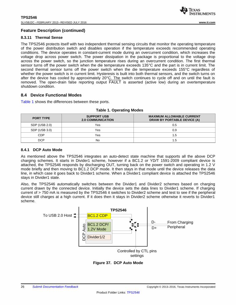
Also, the TPS2546 automatically switches between the Divider1 and Divider2 schemes based on chargingcurrent drawn by the connected device. Initially the device sets the data lines to Divider1 scheme. If chargingcurrent of > 750 mA is measured by the TPS2546 it switches to Divider2 scheme and test to see if the peripheraldevice still charges at a high current. If it does then it stays in Divider2 scheme otherwise it reverts to Divider1scheme.
Figure 37. DCP Auto Mode
27
TPS2546www.ti.com SLVSBJ2C –FEBRUARY 2013–REVISED JULY 2016
Product Folder Links: TPS2546
Submit Documentation FeedbackCopyright © 2013–2016, Texas Instruments Incorporated
8.4.2 DCP Forced Shorted / DCP Forced Divider1In this mode the device is permanently set to one of the DCP schemes (BC1.2/ YD/T 1591-2009 or Divider1) ascommanded by its control pin setting per Table 3.
8.4.3 High-Bandwidth Data Line SwitchThe TPS2546 passes the D+ and D– data lines through the device to enable monitoring and handshaking whilesupporting charging operation. A wide bandwidth signal switch is used, allowing data to pass through the devicewithout corrupting signal integrity. The data line switches are turned on in any of CDP or SDP operating modes.The EN input also needs to be at logic High for the data line switches to be enabled.
NOTE• While in CDP mode, the data switches are ON even while CDP handshaking is
occurring• The data line switches are OFF if EN or all CTL pins are held low, or if in DCP mode.
They are not automatically turned off if the power switch (IN to OUT) is in current limit• The data switches are for USB 2.0 differential pair only. In the case of a USB 3.0 host,
the super speed differential pairs must be routed directly to the USB connector withoutpassing through the TPS2546
• Data switches are OFF during OUT (VBUS) discharge
Table 2 can be used as an aid to program the TPS2546 per system states however not restricted to belowsettings only.
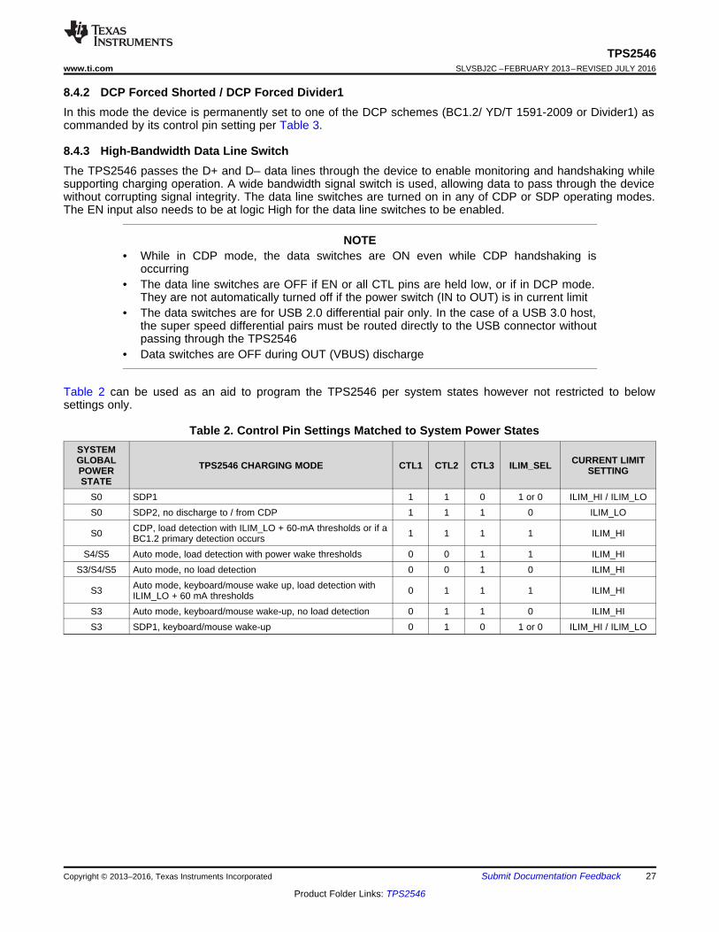
Table 2. Control Pin Settings Matched to System Power StatesSYSTEMGLOBALPOWERSTATE
TPS2546 CHARGING MODE CTL1 CTL2 CTL3 ILIM_SEL CURRENT LIMITSETTING
S0 SDP1 1 1 0 1 or 0 ILIM_HI / ILIM_LOS0 SDP2, no discharge to / from CDP 1 1 1 0 ILIM_LO
S0 CDP, load detection with ILIM_LO + 60-mA thresholds or if aBC1.2 primary detection occurs 1 1 1 1 ILIM_HI
S4/S5 Auto mode, load detection with power wake thresholds 0 0 1 1 ILIM_HIS3/S4/S5 Auto mode, no load detection 0 0 1 0 ILIM_HI
S3 Auto mode, keyboard/mouse wake up, load detection withILIM_LO + 60 mA thresholds 0 1 1 1 ILIM_HI
S3 Auto mode, keyboard/mouse wake-up, no load detection 0 1 1 0 ILIM_HIS3 SDP1, keyboard/mouse wake-up 0 1 0 1 or 0 ILIM_HI / ILIM_LO
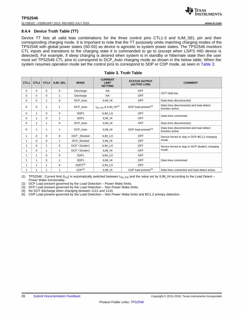
28
TPS2546SLVSBJ2C –FEBRUARY 2013–REVISED JULY 2016 www.ti.com
Product Folder Links: TPS2546
Submit Documentation Feedback Copyright © 2013–2016, Texas Instruments Incorporated
(1) TPS2546 : Current limit (IOS) is automatically switched between IOS_PW and the value set by ILIM_HI according to the Load Detect –Power Wake functionality.
(2) DCP Load present governed by the Load Detection – Power Wake limits.(3) DCP Load present governed by the Load Detection – Non Power Wake limits.(4) No OUT discharge when changing between 1111 and 1110.(5) CDP Load present governed by the Load Detection – Non Power Wake limits and BC1.2 primary detection.
8.4.4 Device Truth Table (TT)Device TT lists all valid bias combinations for the three control pins CTL1-3 and ILIM_SEL pin and theircorresponding charging mode. It is important to note that the TT purposely omits matching charging modes of theTPS2546 with global power states (S0-S5) as device is agnostic to system power states. The TPS2546 monitorsCTL inputs and transitions to the charging state it is commanded to go to (except when LS/FS HID device isdetected). For example, if sleep charging is desired when system is in standby or hibernate state then the usermust set TPS2546 CTL pins to correspond to DCP_Auto charging mode as shown in the below table. When thesystem resumes operation mode set the control pins to correspond to SDP or CDP mode, as seen in Table 3.
Table 3. Truth Table
CTL1 CTL2 CTL3 ILIM_SEL MODECURRENT
LIMITSETTING
STATUS OUTPUT(ACTIVE LOW) COMMENT
0 0 0 0 Discharge NA OFFOUT held low.
0 0 0 1 Discharge NA OFF
0 0 1 0 DCP_Auto ILIM_HI OFF Data lines disconnected.
0 0 1 1 DCP_Auto IOS_PW & ILIM_HI (1) DCP load present (2) Data lines disconnected and load detectfunction active.
0 1 0 0 SDP1 ILIM_LO OFFData lines connected.
0 1 0 1 SDP1 ILIM_HI OFF
0 1 1 0 DCP_Auto ILIM_HI OFF Data lines disconnected.
0 1 1 1 DCP_Auto ILIM_HI DCP load present (3) Data lines disconnected and load detectfunction active.
1 0 0 0 DCP _Shorted ILIM_LO OFF Device forced to stay in DCP BC1.2 chargingmode.1 0 0 1 DCP_Shorted ILIM_HI OFF
1 0 1 0 DCP / Divider1 ILIM_LO OFF Device forced to stay in DCP divider1 chargingmode.1 0 1 1 DCP / Divider1 ILIM_HI OFF
1 1 0 0 SDP1 ILIM_LO OFF
Data lines connected.1 1 0 1 SDP1 ILIM_HI OFF
1 1 1 0 SDP2 (4) ILIM_LO OFF
1 1 1 1 CDP (4) ILIM_HI CDP load present (5) Data lines connected and load detect active.
Reset
DCH
CDP
(1111)
SDP1
(110X/
010X)
Discharge
SDP1
CDP
Not CDP
Or SDP2
DCH
Done
DCP Forced(DCP Shorted or
Divider 1)
DCP_SHORT/
DCP_DIVIDER
DCP Auto(Shorted/1.2V Pull-Up/
Divider 1/Divider 2)
DCP_Auto DCP_SHT/
DCP_DIV
DCH/SDP/CDP
DCH/SDP/CDP
Not SDP1
DCP_Auto
SDP2
SampleCTL Pins
SDP2
(1110)
SDP2
(1110)
CDP
(1111) Not SDP2
Or CDP
Copyright © 2016, Texas Instruments Incorporated
29
TPS2546www.ti.com SLVSBJ2C –FEBRUARY 2013–REVISED JULY 2016
Product Folder Links: TPS2546
Submit Documentation FeedbackCopyright © 2013–2016, Texas Instruments Incorporated
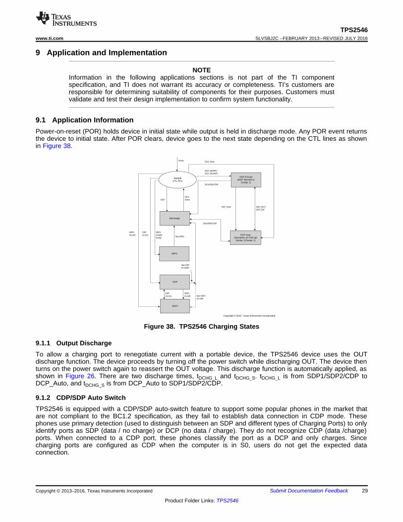
9 Application and Implementation
NOTEInformation in the following applications sections is not part of the TI componentspecification, and TI does not warrant its accuracy or completeness. TI’s customers areresponsible for determining suitability of components for their purposes. Customers mustvalidate and test their design implementation to confirm system functionality.
9.1 Application InformationPower-on-reset (POR) holds device in initial state while output is held in discharge mode. Any POR event returnsthe device to initial state. After POR clears, device goes to the next state depending on the CTL lines as shownin Figure 38.
Figure 38. TPS2546 Charging States
9.1.1 Output DischargeTo allow a charging port to renegotiate current with a portable device, the TPS2546 device uses the OUTdischarge function. The device proceeds by turning off the power switch while discharging OUT. The device thenturns on the power switch again to reassert the OUT voltage. This discharge function is automatically applied, asshown in Figure 26. There are two discharge times, tDCHG_L and tDCHG_S. tDCHG_L is from SDP1/SDP2/CDP toDCP_Auto, and tDCHG_S is from DCP_Auto to SDP1/SDP2/CDP.
9.1.2 CDP/SDP Auto SwitchTPS2546 is equipped with a CDP/SDP auto-switch feature to support some popular phones in the market thatare not compliant to the BC1.2 specification, as they fail to establish data connection in CDP mode. Thesephones use primary detection (used to distinguish between an SDP and different types of Charging Ports) to onlyidentify ports as SDP (data / no charge) or DCP (no data / charge). They do not recognize CDP (data /charge)ports. When connected to a CDP port, these phones classify the port as a DCP and only charges. Sincecharging ports are configured as CDP when the computer is in S0, users do not get the expected dataconnection.
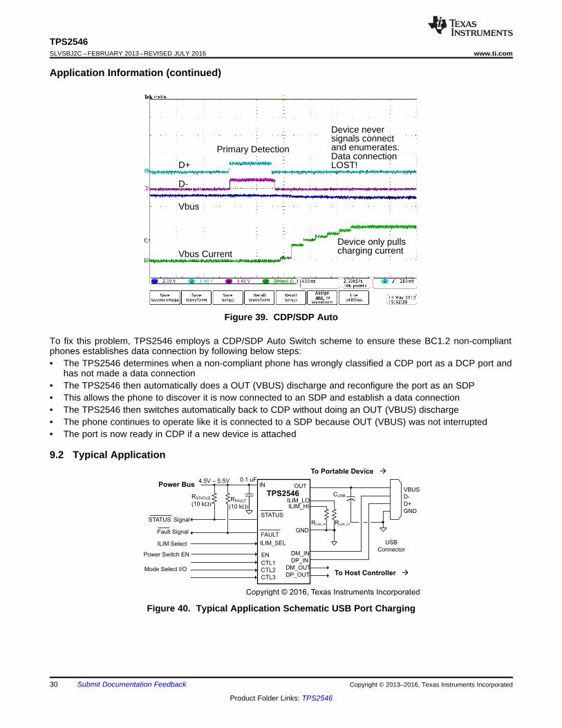
OUT
GNDFAULT
ILIM_LO
EN
RILIM_LO
RSTATUS
(10 kW)
Power Switch EN
4.5V – 5.5V
TPS2546
0.1 uF
CUSB
Fault Signal
DM_IN
DP_IN
VBUS
D-
D+
GND
USB
Connector
To Portable Device à
Power Bus
CTL1
CTL2
CTL3
ILIM_SELILIM Select
DM_OUT
DP_OUT To Host Controller àMode Select I/O
IN
STATUSSTATUS Signal
RILIM_HI
ILIM_HI
RFAULT
(10 kW)
Copyright © 2016, Texas Instruments Incorporated
D+
D-
Primary Detection
Device never signals connect and enumerates.Data connection LOST!
Device only pulls charging current
Vbus
Vbus Current
30
TPS2546SLVSBJ2C –FEBRUARY 2013–REVISED JULY 2016 www.ti.com
Product Folder Links: TPS2546
Submit Documentation Feedback Copyright © 2013–2016, Texas Instruments Incorporated
Application Information (continued)
Figure 39. CDP/SDP Auto
To fix this problem, TPS2546 employs a CDP/SDP Auto Switch scheme to ensure these BC1.2 non-compliantphones establishes data connection by following below steps:• The TPS2546 determines when a non-compliant phone has wrongly classified a CDP port as a DCP port and
has not made a data connection• The TPS2546 then automatically does a OUT (VBUS) discharge and reconfigure the port as an SDP• This allows the phone to discover it is now connected to an SDP and establish a data connection• The TPS2546 then switches automatically back to CDP without doing an OUT (VBUS) discharge• The phone continues to operate like it is connected to a SDP because OUT (VBUS) was not interrupted• The port is now ready in CDP if a new device is attached
9.2 Typical Application
Figure 40. Typical Application Schematic USB Port Charging
0
500
1000
1500
2000
2500
3000
3500
0 80 160 240 320 400 480 560 640 720 800Current-Limit Programming Resistor (kΩ)
OU
T S
hort
Circ
uit C
urre
nt L
imit
(m
A)
Full RILIM_XX Range
G018
OS_typILIM_XX
50,250I (mA) =
R (kΩ)
31
TPS2546www.ti.com SLVSBJ2C –FEBRUARY 2013–REVISED JULY 2016
Product Folder Links: TPS2546
Submit Documentation FeedbackCopyright © 2013–2016, Texas Instruments Incorporated
Typical Application (continued)9.2.1 Design RequirementsFor this design example, use the parameters listed in Table 4.
Table 4. Design ParametersDESIGN PARAMETER EXAMPLE VALUE
Input voltage, V(IN) 5 VOutput voltage, V(DC) 5 VMaximum continuous output current, I(OUT) 2.5 ACurrent limit, I(LIM_LO) at RILIM_LO = 80.6 kΩ 0.625 ACurrent Limit, I(LIM_HI) at RILIM_HI = 16.9 kΩ 2.97 A
9.2.2 Detailed Design Procedure
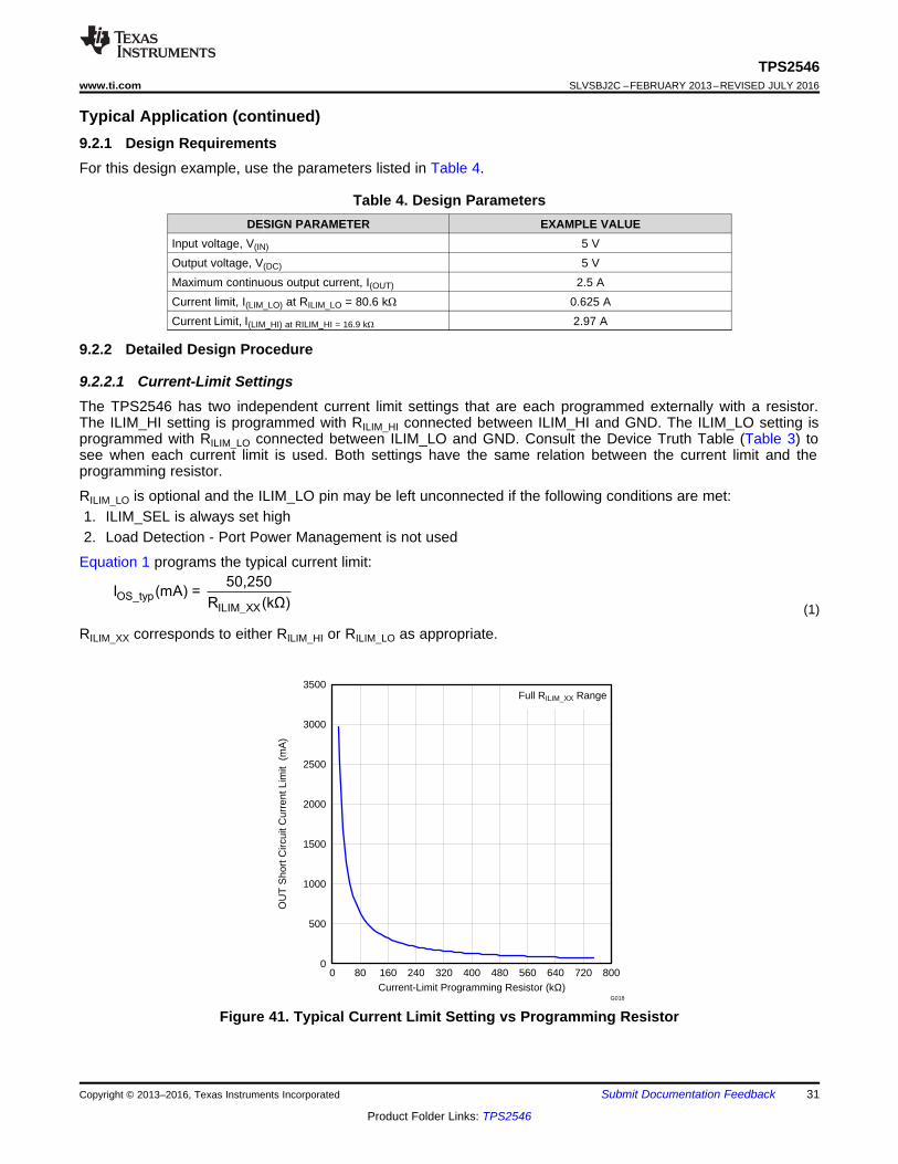
9.2.2.1 Current-Limit SettingsThe TPS2546 has two independent current limit settings that are each programmed externally with a resistor.The ILIM_HI setting is programmed with RILIM_HI connected between ILIM_HI and GND. The ILIM_LO setting isprogrammed with RILIM_LO connected between ILIM_LO and GND. Consult the Device Truth Table (Table 3) tosee when each current limit is used. Both settings have the same relation between the current limit and theprogramming resistor.
RILIM_LO is optional and the ILIM_LO pin may be left unconnected if the following conditions are met:1. ILIM_SEL is always set high2. Load Detection - Port Power Management is not used
Equation 1 programs the typical current limit:
(1)
RILIM_XX corresponds to either RILIM_HI or RILIM_LO as appropriate.
Figure 41. Typical Current Limit Setting vs Programming Resistor
0
500
1000
1500
2000
2500
3000
3500
0 10 20 30 40 50 60 70 80 90 100Current-Limit Programming Resistor (kΩ)
OU
T S
hort
Circ
uit C
urre
nt L
imit
(m
A)
Min IOSTyp IOSMax IOS
Lower RILIM_XX Range
G019
0
100
200
300
400
500
600
100 150 200 250 300 350 400 450 500 550 600 650 700 750Current-Limit Programming Resistor (kΩ)
OU
T S
hort
Circ
uit C
urre
nt L
imit
(m
A)
Min IOSTyp IOSMax IOS
Upper RILIM_XX Range
G020
OS_max 1.0139ILIM_XX
55,325I (mA) = + 30
(R (kΩ))
OS_min 0.98437ILIM_XX
45,271I (mA) = - 30
(R (kΩ))
32
TPS2546SLVSBJ2C –FEBRUARY 2013–REVISED JULY 2016 www.ti.com
Product Folder Links: TPS2546
Submit Documentation Feedback Copyright © 2013–2016, Texas Instruments Incorporated
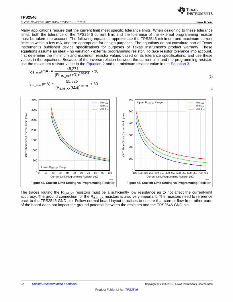
Many applications require that the current limit meet specific tolerance limits. When designing to these tolerancelimits, both the tolerance of the TPS2546 current limit and the tolerance of the external programming resistormust be taken into account. The following equations approximate the TPS2546 minimum and maximum currentlimits to within a few mA, and are appropriate for design purposes. The equations do not constitute part of TexasInstrument's published device specifications for purposes of Texas Instrument's product warranty. Theseequations assume an ideal - no variation - external programming resistor. To take resistor tolerance into account,first determine the minimum and maximum resistor values based on its tolerance specifications, and use thesevalues in the equations. Because of the inverse relation between the current limit and the programming resistor,use the maximum resistor value in the Equation 2 and the minimum resistor value in the Equation 3.
(2)
(3)
Figure 42. Current Limit Setting vs Programming Resistor Figure 43. Current Limit Setting vs Programming Resistor
The traces routing the RILIM_XX resistors must be a sufficiently low resistance as to not affect the current-limitaccuracy. The ground connection for the RILIM_XX resistors is also very important. The resistors need to referenceback to the TPS2546 GND pin. Follow normal board layout practices to ensure that current flow from other partsof the board does not impact the ground potential between the resistors and the TPS2546 GND pin.
10
0 m
A/d
iv
D+ – 1.00 V/divD– – 1.00 V/div
VBUS – 2.00 V/divVBUS Current – 500 mA/div
D+
D–
VBUS
VBUS Current
Devicedetects
connectionto CDP
Device detectsconnection to a
charging port
USB 2.0enumeration
Device pulls correctcharging current
1.0
0A
/div
5.00 ms/div
VBUS Current
500 m
A/d
iv
5.00 ms/div
VBUS Current
33
TPS2546www.ti.com SLVSBJ2C –FEBRUARY 2013–REVISED JULY 2016
Product Folder Links: TPS2546
Submit Documentation FeedbackCopyright © 2013–2016, Texas Instruments Incorporated
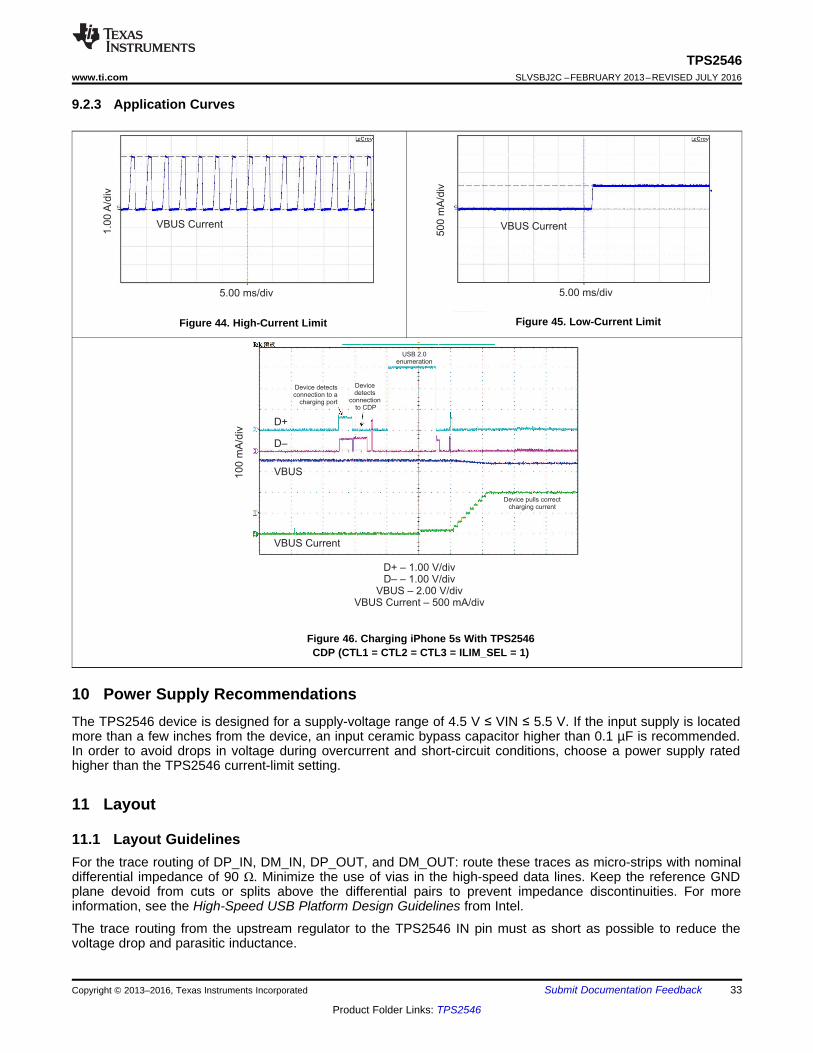
9.2.3 Application Curves
Figure 44. High-Current Limit Figure 45. Low-Current Limit
Figure 46. Charging iPhone 5s With TPS2546CDP (CTL1 = CTL2 = CTL3 = ILIM_SEL = 1)
10 Power Supply RecommendationsThe TPS2546 device is designed for a supply-voltage range of 4.5 V ≤ VIN ≤ 5.5 V. If the input supply is locatedmore than a few inches from the device, an input ceramic bypass capacitor higher than 0.1 µF is recommended.In order to avoid drops in voltage during overcurrent and short-circuit conditions, choose a power supply ratedhigher than the TPS2546 current-limit setting.
11 Layout
11.1 Layout GuidelinesFor the trace routing of DP_IN, DM_IN, DP_OUT, and DM_OUT: route these traces as micro-strips with nominaldifferential impedance of 90 Ω. Minimize the use of vias in the high-speed data lines. Keep the reference GNDplane devoid from cuts or splits above the differential pairs to prevent impedance discontinuities. For moreinformation, see the High-Speed USB Platform Design Guidelines from Intel.
The trace routing from the upstream regulator to the TPS2546 IN pin must as short as possible to reduce thevoltage drop and parasitic inductance.
11
1
2
3
4
5 6 7 8
9
10
12
13141516
IN
DM_OUT
DP_OUT
CLT
1
CT
L2
OUT
ILIM_SEL
DP_IN
DM_IN
ILIM
_HI
FA
ULT
GN
DIL
IMI_
LO
EN
CT
L3
STATUS
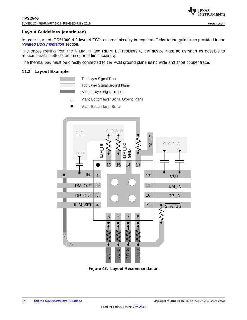
Via to Bottom layer Signal Ground Plane
Via to Bottom layer Signal
Top Layer Signal Trace
Top Layer Signal Ground Plane
Bottom Layer Signal Trace
xxxxx
xx
x
xxx
34
TPS2546SLVSBJ2C –FEBRUARY 2013–REVISED JULY 2016 www.ti.com
Product Folder Links: TPS2546
Submit Documentation Feedback Copyright © 2013–2016, Texas Instruments Incorporated
Layout Guidelines (continued)In order to meet IEC61000-4-2 level 4 ESD, external circuitry is required. Refer to the guidelines provided in theRelated Documentation section.
The traces routing from the RILIM_HI and RILIM_LO resistors to the device must be as short as possible toreduce parasitic effects on the current-limit accuracy.
The thermal pad must be directly connected to the PCB ground plane using wide and short copper trace.
11.2 Layout Example
Figure 47. Layout Recommendation
35
TPS2546www.ti.com SLVSBJ2C –FEBRUARY 2013–REVISED JULY 2016
Product Folder Links: TPS2546
Submit Documentation FeedbackCopyright © 2013–2016, Texas Instruments Incorporated
12 Device and Documentation Support
12.1 Documentation Support
12.1.1 Related DocumentationFor related documentation see:
Effective System ESD Protection for TPS254x USB Charging Port Controllers, SLVA796.
High Speed USB Platform Design Guidelines, Intel (www.usb.org/developers/docs/hs_usb_pdg_r1_0.pdf)
USB 2.0 Specifications (www.usb.org/developers/docs/usb20_docs/#usb20spec)
BC1.2 Battery Charging Specification (kinetis.pl/sites/default/files/BC1.2_FINAL.pdf)
12.2 Receiving Notification of Documentation UpdatesTo receive notification of documentation updates, navigate to the device product folder on ti.com. In the upperright corner, click on Alert me to register and receive a weekly digest of any product information that haschanged. For change details, review the revision history included in any revised document.
12.3 Community ResourcesThe following links connect to TI community resources. Linked contents are provided "AS IS" by the respectivecontributors. They do not constitute TI specifications and do not necessarily reflect TI's views; see TI's Terms ofUse.
TI E2E™ Online Community TI's Engineer-to-Engineer (E2E) Community. Created to foster collaborationamong engineers. At e2e.ti.com, you can ask questions, share knowledge, explore ideas and helpsolve problems with fellow engineers.
Design Support TI's Design Support Quickly find helpful E2E forums along with design support tools andcontact information for technical support.
12.4 TrademarksE2E is a trademark of Texas Instruments.All other trademarks are the property of their respective owners.
12.5 Electrostatic Discharge CautionThese devices have limited built-in ESD protection. The leads should be shorted together or the device placed in conductive foamduring storage or handling to prevent electrostatic damage to the MOS gates.
12.6 GlossarySLYZ022 — TI Glossary.
This glossary lists and explains terms, acronyms, and definitions.
13 Mechanical, Packaging, and Orderable InformationThe following pages include mechanical, packaging, and orderable information. This information is the mostcurrent data available for the designated devices. This data is subject to change without notice and revision ofthis document. For browser-based versions of this data sheet, refer to the left-hand navigation.
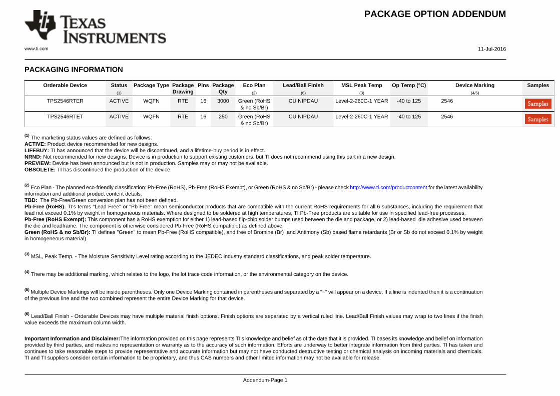
PACKAGE OPTION ADDENDUM
www.ti.com 11-Jul-2016
Addendum-Page 1
PACKAGING INFORMATION
Orderable Device Status(1)
Package Type PackageDrawing
Pins PackageQty
Eco Plan(2)
Lead/Ball Finish(6)
MSL Peak Temp(3)
Op Temp (°C) Device Marking(4/5)
Samples
TPS2546RTER ACTIVE WQFN RTE 16 3000 Green (RoHS& no Sb/Br)
CU NIPDAU Level-2-260C-1 YEAR -40 to 125 2546
TPS2546RTET ACTIVE WQFN RTE 16 250 Green (RoHS& no Sb/Br)
CU NIPDAU Level-2-260C-1 YEAR -40 to 125 2546
(1) The marketing status values are defined as follows:ACTIVE: Product device recommended for new designs.LIFEBUY: TI has announced that the device will be discontinued, and a lifetime-buy period is in effect.NRND: Not recommended for new designs. Device is in production to support existing customers, but TI does not recommend using this part in a new design.PREVIEW: Device has been announced but is not in production. Samples may or may not be available.OBSOLETE: TI has discontinued the production of the device.
(2) Eco Plan - The planned eco-friendly classification: Pb-Free (RoHS), Pb-Free (RoHS Exempt), or Green (RoHS & no Sb/Br) - please check http://www.ti.com/productcontent for the latest availabilityinformation and additional product content details.TBD: The Pb-Free/Green conversion plan has not been defined.Pb-Free (RoHS): TI's terms "Lead-Free" or "Pb-Free" mean semiconductor products that are compatible with the current RoHS requirements for all 6 substances, including the requirement thatlead not exceed 0.1% by weight in homogeneous materials. Where designed to be soldered at high temperatures, TI Pb-Free products are suitable for use in specified lead-free processes.Pb-Free (RoHS Exempt): This component has a RoHS exemption for either 1) lead-based flip-chip solder bumps used between the die and package, or 2) lead-based die adhesive used betweenthe die and leadframe. The component is otherwise considered Pb-Free (RoHS compatible) as defined above.Green (RoHS & no Sb/Br): TI defines "Green" to mean Pb-Free (RoHS compatible), and free of Bromine (Br) and Antimony (Sb) based flame retardants (Br or Sb do not exceed 0.1% by weightin homogeneous material)
(3) MSL, Peak Temp. - The Moisture Sensitivity Level rating according to the JEDEC industry standard classifications, and peak solder temperature.
(4) There may be additional marking, which relates to the logo, the lot trace code information, or the environmental category on the device.
(5) Multiple Device Markings will be inside parentheses. Only one Device Marking contained in parentheses and separated by a "~" will appear on a device. If a line is indented then it is a continuationof the previous line and the two combined represent the entire Device Marking for that device.
(6) Lead/Ball Finish - Orderable Devices may have multiple material finish options. Finish options are separated by a vertical ruled line. Lead/Ball Finish values may wrap to two lines if the finishvalue exceeds the maximum column width.
Important Information and Disclaimer:The information provided on this page represents TI's knowledge and belief as of the date that it is provided. TI bases its knowledge and belief on informationprovided by third parties, and makes no representation or warranty as to the accuracy of such information. Efforts are underway to better integrate information from third parties. TI has taken andcontinues to take reasonable steps to provide representative and accurate information but may not have conducted destructive testing or chemical analysis on incoming materials and chemicals.TI and TI suppliers consider certain information to be proprietary, and thus CAS numbers and other limited information may not be available for release.
PACKAGE OPTION ADDENDUM
www.ti.com 11-Jul-2016
Addendum-Page 2
In no event shall TI's liability arising out of such information exceed the total purchase price of the TI part(s) at issue in this document sold by TI to Customer on an annual basis.
OTHER QUALIFIED VERSIONS OF TPS2546 :
• Automotive: TPS2546-Q1
NOTE: Qualified Version Definitions:
• Automotive - Q100 devices qualified for high-reliability automotive applications targeting zero defects
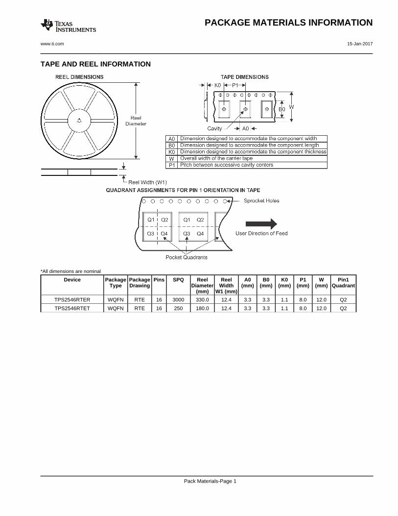
TAPE AND REEL INFORMATION
*All dimensions are nominal
Device PackageType
PackageDrawing
Pins SPQ ReelDiameter
(mm)
ReelWidth
W1 (mm)
A0(mm)
B0(mm)
K0(mm)
P1(mm)
W(mm)
Pin1Quadrant
TPS2546RTER WQFN RTE 16 3000 330.0 12.4 3.3 3.3 1.1 8.0 12.0 Q2
TPS2546RTET WQFN RTE 16 250 180.0 12.4 3.3 3.3 1.1 8.0 12.0 Q2
PACKAGE MATERIALS INFORMATION
www.ti.com 15-Jan-2017
Pack Materials-Page 1
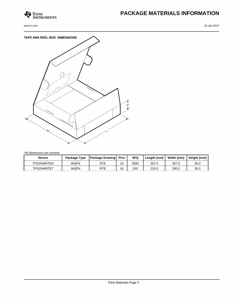
*All dimensions are nominal
Device Package Type Package Drawing Pins SPQ Length (mm) Width (mm) Height (mm)
TPS2546RTER WQFN RTE 16 3000 367.0 367.0 35.0
TPS2546RTET WQFN RTE 16 250 210.0 185.0 35.0
PACKAGE MATERIALS INFORMATION
www.ti.com 15-Jan-2017
Pack Materials-Page 2
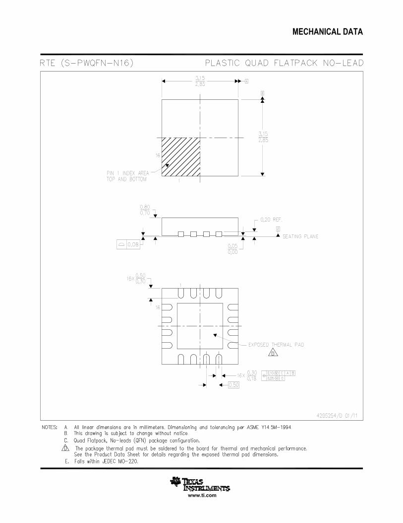
IMPORTANT NOTICE
Texas Instruments Incorporated (TI) reserves the right to make corrections, enhancements, improvements and other changes to itssemiconductor products and services per JESD46, latest issue, and to discontinue any product or service per JESD48, latest issue. Buyersshould obtain the latest relevant information before placing orders and should verify that such information is current and complete.TI’s published terms of sale for semiconductor products (http://www.ti.com/sc/docs/stdterms.htm) apply to the sale of packaged integratedcircuit products that TI has qualified and released to market. Additional terms may apply to the use or sale of other types of TI products andservices.Reproduction of significant portions of TI information in TI data sheets is permissible only if reproduction is without alteration and isaccompanied by all associated warranties, conditions, limitations, and notices. TI is not responsible or liable for such reproduceddocumentation. Information of third parties may be subject to additional restrictions. Resale of TI products or services with statementsdifferent from or beyond the parameters stated by TI for that product or service voids all express and any implied warranties for theassociated TI product or service and is an unfair and deceptive business practice. TI is not responsible or liable for any such statements.Buyers and others who are developing systems that incorporate TI products (collectively, “Designers”) understand and agree that Designersremain responsible for using their independent analysis, evaluation and judgment in designing their applications and that Designers havefull and exclusive responsibility to assure the safety of Designers' applications and compliance of their applications (and of all TI productsused in or for Designers’ applications) with all applicable regulations, laws and other applicable requirements. Designer represents that, withrespect to their applications, Designer has all the necessary expertise to create and implement safeguards that (1) anticipate dangerousconsequences of failures, (2) monitor failures and their consequences, and (3) lessen the likelihood of failures that might cause harm andtake appropriate actions. Designer agrees that prior to using or distributing any applications that include TI products, Designer willthoroughly test such applications and the functionality of such TI products as used in such applications.TI’s provision of technical, application or other design advice, quality characterization, reliability data or other services or information,including, but not limited to, reference designs and materials relating to evaluation modules, (collectively, “TI Resources”) are intended toassist designers who are developing applications that incorporate TI products; by downloading, accessing or using TI Resources in anyway, Designer (individually or, if Designer is acting on behalf of a company, Designer’s company) agrees to use any particular TI Resourcesolely for this purpose and subject to the terms of this Notice.TI’s provision of TI Resources does not expand or otherwise alter TI’s applicable published warranties or warranty disclaimers for TIproducts, and no additional obligations or liabilities arise from TI providing such TI Resources. TI reserves the right to make corrections,enhancements, improvements and other changes to its TI Resources. TI has not conducted any testing other than that specificallydescribed in the published documentation for a particular TI Resource.Designer is authorized to use, copy and modify any individual TI Resource only in connection with the development of applications thatinclude the TI product(s) identified in such TI Resource. NO OTHER LICENSE, EXPRESS OR IMPLIED, BY ESTOPPEL OR OTHERWISETO ANY OTHER TI INTELLECTUAL PROPERTY RIGHT, AND NO LICENSE TO ANY TECHNOLOGY OR INTELLECTUAL PROPERTYRIGHT OF TI OR ANY THIRD PARTY IS GRANTED HEREIN, including but not limited to any patent right, copyright, mask work right, orother intellectual property right relating to any combination, machine, or process in which TI products or services are used. Informationregarding or referencing third-party products or services does not constitute a license to use such products or services, or a warranty orendorsement thereof. Use of TI Resources may require a license from a third party under the patents or other intellectual property of thethird party, or a license from TI under the patents or other intellectual property of TI.TI RESOURCES ARE PROVIDED “AS IS” AND WITH ALL FAULTS. TI DISCLAIMS ALL OTHER WARRANTIES ORREPRESENTATIONS, EXPRESS OR IMPLIED, REGARDING RESOURCES OR USE THEREOF, INCLUDING BUT NOT LIMITED TOACCURACY OR COMPLETENESS, TITLE, ANY EPIDEMIC FAILURE WARRANTY AND ANY IMPLIED WARRANTIES OFMERCHANTABILITY, FITNESS FOR A PARTICULAR PURPOSE, AND NON-INFRINGEMENT OF ANY THIRD PARTY INTELLECTUALPROPERTY RIGHTS. TI SHALL NOT BE LIABLE FOR AND SHALL NOT DEFEND OR INDEMNIFY DESIGNER AGAINST ANY CLAIM,INCLUDING BUT NOT LIMITED TO ANY INFRINGEMENT CLAIM THAT RELATES TO OR IS BASED ON ANY COMBINATION OFPRODUCTS EVEN IF DESCRIBED IN TI RESOURCES OR OTHERWISE. IN NO EVENT SHALL TI BE LIABLE FOR ANY ACTUAL,DIRECT, SPECIAL, COLLATERAL, INDIRECT, PUNITIVE, INCIDENTAL, CONSEQUENTIAL OR EXEMPLARY DAMAGES INCONNECTION WITH OR ARISING OUT OF TI RESOURCES OR USE THEREOF, AND REGARDLESS OF WHETHER TI HAS BEENADVISED OF THE POSSIBILITY OF SUCH DAMAGES.Unless TI has explicitly designated an individual product as meeting the requirements of a particular industry standard (e.g., ISO/TS 16949and ISO 26262), TI is not responsible for any failure to meet such industry standard requirements.Where TI specifically promotes products as facilitating functional safety or as compliant with industry functional safety standards, suchproducts are intended to help enable customers to design and create their own applications that meet applicable functional safety standardsand requirements. Using products in an application does not by itself establish any safety features in the application. Designers mustensure compliance with safety-related requirements and standards applicable to their applications. Designer may not use any TI products inlife-critical medical equipment unless authorized officers of the parties have executed a special contract specifically governing such use.Life-critical medical equipment is medical equipment where failure of such equipment would cause serious bodily injury or death (e.g., lifesupport, pacemakers, defibrillators, heart pumps, neurostimulators, and implantables). Such equipment includes, without limitation, allmedical devices identified by the U.S. Food and Drug Administration as Class III devices and equivalent classifications outside the U.S.TI may expressly designate certain products as completing a particular qualification (e.g., Q100, Military Grade, or Enhanced Product).Designers agree that it has the necessary expertise to select the product with the appropriate qualification designation for their applicationsand that proper product selection is at Designers’ own risk. Designers are solely responsible for compliance with all legal and regulatoryrequirements in connection with such selection.Designer will fully indemnify TI and its representatives against any damages, costs, losses, and/or liabilities arising out of Designer’s non-compliance with the terms and provisions of this Notice.
Mailing Address: Texas Instruments, Post Office Box 655303, Dallas, Texas 75265Copyright © 2017, Texas Instruments Incorporated