Embed Size (px)
Citation preview

BST
SW
PGND
VOUT
VIN
EN
COMP
VREF
TPS53317
REFIN
V5IN
PGOOD
MODE
GND
PGOOD
VTT
5VIN
UDG-11105
PowerPAD
DDR VDDQ IN
EN
Product
Folder
Sample &Buy
Technical
Documents
Tools &
Software
Support &Community
TPS53317SLUSAK4D –JUNE 2011–REVISED JULY 2015
TPS53317 6-A Output, D-CAP+ Mode, Synchronous Step-Down,Integrated-FET Converter for DDR Memory Termination
1 Features 3 DescriptionThe TPS53317 device is a FET-integrated
1• TI proprietary Integrated MOSFET and Packagingsynchronous buck regulator designed mainly for DDRTechnologytermination. It can provide a regulated output at ½
• Supports DDR Memory Termination with up to 6-A VDDQ with both sink and source capability. TheContinuous Output Source or Sink Current TPS53317 device employs D-CAP+™ mode
operation that provides ease of use, low external• External Trackingcomponent count and fast transient response. The• Minimum External Components Countdevice can also be used for other point-of-load (POL)
• 1-V to 6-V Conversion Voltage regulation applications requiring up to 6 A. In• D-CAP+™ Mode Architecture addition, the device supports full, 6-A, output sinking
current capability with tight voltage regulation.• Supports All MLCC Output Capacitors andSP/POSCAP The device features two switching frequency settings
(600 kHz and 1 MHz), integrated droop support,• Selectable SKIP Mode or Forced CCMexternal tracking capability, pre-bias startup, output• Optimized Efficiency at Light and Heavy Loadssoft discharge, integrated bootstrap switch, power
• Selectable 600-kHz or 1-MHz Switching good function, V5IN pin UVLO protection, andFrequency supports both ceramic and SP/POSCAP capacitors. It
supports input voltages up to 6.0 V, and output• Selectable Overcurrent Limit (OCL)voltages adjustable from 0.6 V to 2.0 V.• Overvoltage, Over-Temperature and Hiccup
Undervoltage Protection The TPS53317 device is available in the 3.5 mm × 4mm, 20-pin, VQFN package (Green RoHs compliant• Adjustable Output Voltage from 0.6 V to 2 Vand Pb free) with TI proprietary Integrated MOSFET• 3.5 mm × 4 mm, 20-Pin VQFN Package and packaging technology and is specified from–40°C to 85°C.2 Applications
Device Information(1)• Memory Termination Regulator for DDR, DDR2,DDR3, DDR3L, and DDR4 PART NUMBER PACKAGE BODY SIZE (NOM)
TPS53317 VQFN (20) 3.50 mm × 4.00 mm• VTT Termination• Low-Voltage Applications for 1-V to 6-V Input (1) For all available packages, see the orderable addendum at
the end of the data sheet.Rails
Simplified Application
1
An IMPORTANT NOTICE at the end of this data sheet addresses availability, warranty, changes, use in safety-critical applications,intellectual property matters and other important disclaimers. PRODUCTION DATA.
TPS53317SLUSAK4D –JUNE 2011–REVISED JULY 2015 www.ti.com
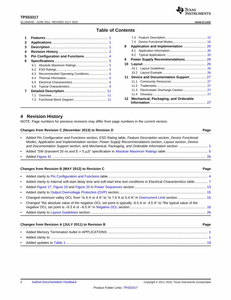
Table of Contents7.3 Feature Description................................................. 121 Features .................................................................. 17.4 Device Functional Modes........................................ 162 Applications ........................................................... 1
8 Application and Implementation ........................ 203 Description ............................................................. 18.1 Application Information............................................ 204 Revision History..................................................... 28.2 Typical Applications ............................................... 205 Pin Configuration and Functions ......................... 4
9 Power Supply Recommendations ...................... 266 Specifications......................................................... 510 Layout................................................................... 266.1 Absolute Maximum Ratings ...................................... 5
10.1 Layout Guidelines ................................................. 266.2 ESD Ratings.............................................................. 510.2 Layout Example .................................................... 266.3 Recommended Operating Conditions....................... 5
11 Device and Documentation Support ................. 276.4 Thermal Information .................................................. 611.1 Community Resources.......................................... 276.5 Electrical Characteristics........................................... 611.2 Trademarks ........................................................... 276.6 Typical Characteristics .............................................. 811.3 Electrostatic Discharge Caution............................ 277 Detailed Description ............................................ 1111.4 Glossary ................................................................ 277.1 Overview ................................................................. 11
12 Mechanical, Packaging, and Orderable7.2 Functional Block Diagram ....................................... 11Information ........................................................... 27
4 Revision HistoryNOTE: Page numbers for previous revisions may differ from page numbers in the current version.
Changes from Revision C (November 2013) to Revision D Page
• Added Pin Configuration and Functions section, ESD Rating table, Feature Description section, Device FunctionalModes, Application and Implementation section, Power Supply Recommendations section, Layout section, Deviceand Documentation Support section, and Mechanical, Packaging, and Orderable Information section .............................. 1
• Added "SW (transient 20 ns and E = 5 µJ)" specification in Absolute Maximum Ratings table ............................................ 5• Added Figure 41 .................................................................................................................................................................. 26
Changes from Revision B (MAY 2012) to Revision C Page
• Added clarity to Pin Configuration and Functions table ......................................................................................................... 4• Added clarity to Internal soft-start delay time and soft-start time test conditions in Electrical Characteristics table.............. 7• Added Figure 17, Figure 19 and Figure 20 in Power Sequences section............................................................................ 13• Added clarity to Output Overvoltage Protection (OVP) section............................................................................................ 15• Changed minimum valley OCL from "is 6 A or 4 A" to "is 7.6 A or 5.4 A" in Overcurrent Limit section. ............................. 15• Changed "the absolute value of the negative OCL set point is typically -6.5 A or -4.5 A" to "the typical value of the
negative OCL set point is –9.3 A or –6.5 A" in Negative OCL section................................................................................. 16• Added clarity to Layout Guidelines section. ......................................................................................................................... 26
Changes from Revision A (JULY 2011) to Revision B Page
• Added Memory Termination bullet in APPLICATIONS .......................................................................................................... 1• Added clarity to ...................................................................................................................................................................... 1• Added updates to Table 1 .................................................................................................................................................... 19
2 Submit Documentation Feedback Copyright © 2011–2015, Texas Instruments Incorporated
Product Folder Links: TPS53317

TPS53317www.ti.com SLUSAK4D –JUNE 2011–REVISED JULY 2015
Changes from Original (JUNE 2011) to Revision A Page
• Changed from "SKIP and Forced CCM" to "SKIP or Forced CCM" in FEATURES............................................................... 1• Changed from "600-kHz and 1-MHz Switching" to "600-kHz or 1-MHz Switching" in FEATURES ....................................... 1• Added clarity to Simplified Application drawing...................................................................................................................... 1• Changed from "fSW = 600 kHz" to " fSW = 1 MHz" for tON(min) in EC table ............................................................................... 7
Copyright © 2011–2015, Texas Instruments Incorporated Submit Documentation Feedback 3
Product Folder Links: TPS53317
15
14
13
12
11
1
2
3
4
5
6
SW
SW
SW
SW
SWVIN
VIN
PGND
PGND
PGND
GN
D
7 8 9 10
20 19 18 17 16
VR
EF
CO
MP
RE
FIN
VO
UT
V5I
N
PG
OO
D
MO
DE
EN
BS
T
Exposed Thermal Pad
TPS53317SLUSAK4D –JUNE 2011–REVISED JULY 2015 www.ti.com
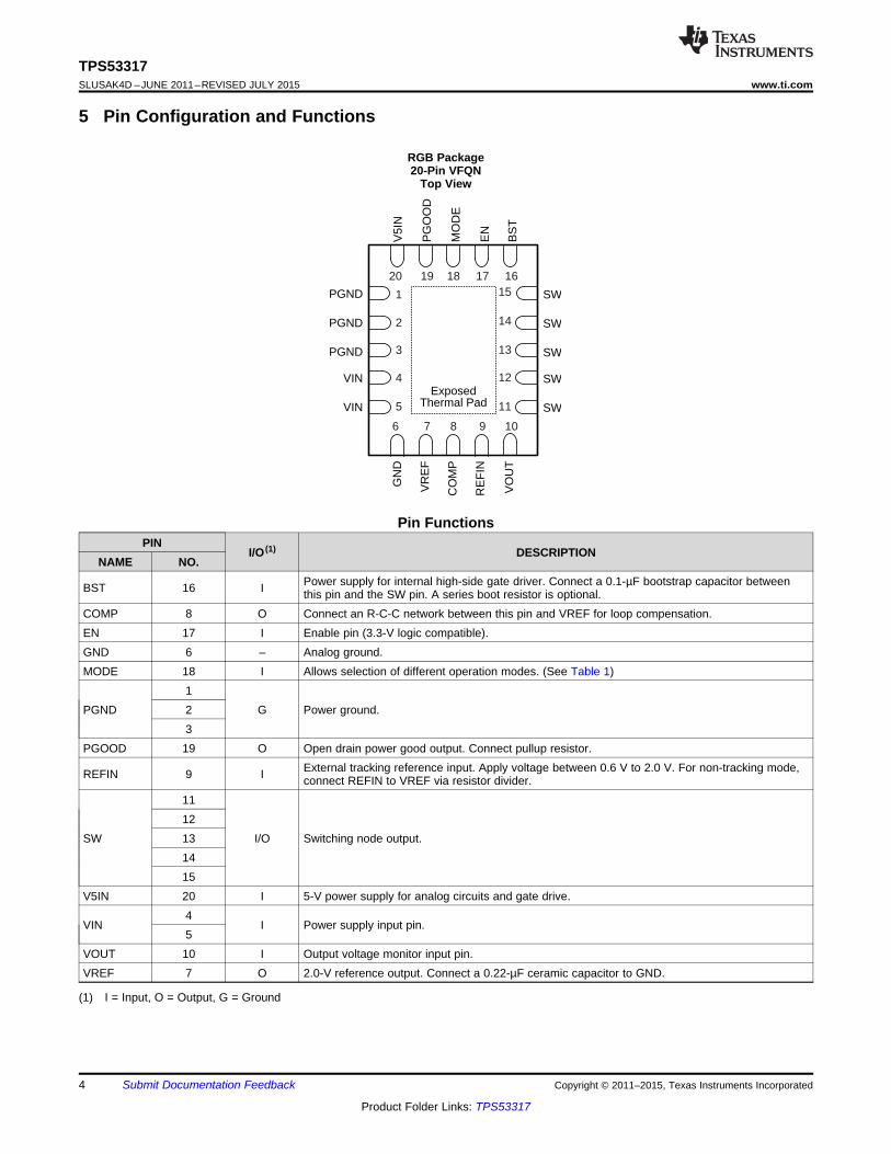
5 Pin Configuration and Functions
RGB Package20-Pin VFQN
Top View
Pin FunctionsPIN
I/O (1) DESCRIPTIONNAME NO.
Power supply for internal high-side gate driver. Connect a 0.1-µF bootstrap capacitor betweenBST 16 I this pin and the SW pin. A series boot resistor is optional.COMP 8 O Connect an R-C-C network between this pin and VREF for loop compensation.EN 17 I Enable pin (3.3-V logic compatible).GND 6 – Analog ground.MODE 18 I Allows selection of different operation modes. (See Table 1)
1PGND 2 G Power ground.
3PGOOD 19 O Open drain power good output. Connect pullup resistor.
External tracking reference input. Apply voltage between 0.6 V to 2.0 V. For non-tracking mode,REFIN 9 I connect REFIN to VREF via resistor divider.1112
SW 13 I/O Switching node output.1415
V5IN 20 I 5-V power supply for analog circuits and gate drive.4
VIN I Power supply input pin.5
VOUT 10 I Output voltage monitor input pin.VREF 7 O 2.0-V reference output. Connect a 0.22-µF ceramic capacitor to GND.
(1) I = Input, O = Output, G = Ground
4 Submit Documentation Feedback Copyright © 2011–2015, Texas Instruments Incorporated
Product Folder Links: TPS53317

TPS53317www.ti.com SLUSAK4D –JUNE 2011–REVISED JULY 2015
6 Specifications
6.1 Absolute Maximum Ratingsover operating free-air temperature range (unless otherwise noted) (1)
MIN MAX UNITBST (with respect to SW), V5IN, VIN –0.3 7BST –0.3 14
Input voltage range EN –0.3 7 VMODE, REFIN –0.3 3.6VOUT –1 3.6SW –2 7SW (transient 20 ns and E = 5 µJ) –3
Output voltage range COMP, VREF –0.3 3.6 VPGOOD –0.3 7PGND –0.3 0.3
Operating junction temperature, TJ –40 150 ˚CLead temperature 1,6 mm (1/16 inch) from case for 10 seconds 300 ˚CStorage temperature, Tstg –55 150 ˚C
(1) Stresses beyond those listed under Absolute Maximum Ratings may cause permanent damage to the device. These are stress ratingsonly, which do not imply functional operation of the device at these or any other conditions beyond those indicated under RecommendedOperating Conditions. Exposure to absolute-maximum-rated conditions for extended periods may affect device reliability.
6.2 ESD RatingsVALUE UNIT
Human-body model (HBM), per ANSI/ESDA/JEDEC JS-001 (1) ±2000V(ESD) Electrostatic discharge V
Charged-device model (CDM), per JEDEC specification JESD22-C101 (2) ±500
(1) JEDEC document JEP155 states that 500-V HBM allows safe manufacturing with a standard ESD control process. Manufacturing withless than 500-V HBM is possible with the necessary precautions. Pins listed as ±2000 V may actually have higher performance.
(2) JEDEC document JEP157 states that 250-V CDM allows safe manufacturing with a standard ESD control process. Manufacturing withless than 250-V CDM is possible with the necessary precautions. Pins listed as ±500 V may actually have higher performance.
6.3 Recommended Operating Conditionsover operating free-air temperature range (unless otherwise noted)
MIN NOM MAX UNITBST (with respect to SW), EN, VIN –0.1 6.5V5IN 4.5 6.5
Input voltage range BST –0.1 13.5 VSW –1.0 6.5VOUT, MODE, REFIN –0.1 3.5COMP –0.1 3.5VREF 2
Output voltage range VPGOOD –0.1 6.5PGND –0.1 0.1
Operating temperature range, TA -40 85 °C
Copyright © 2011–2015, Texas Instruments Incorporated Submit Documentation Feedback 5
Product Folder Links: TPS53317

TPS53317SLUSAK4D –JUNE 2011–REVISED JULY 2015 www.ti.com
6.4 Thermal InformationTPS53317
THERMAL METRIC (1) RGB (VQFN) UNIT20 PINS
RθJA Junction-to-ambient thermal resistance 35.5 °C/WRθJC(top) Junction-to-case (top) thermal resistance 39.6 °C/WRθJB Junction-to-board thermal resistance 12.4 °C/WψJT Junction-to-top characterization parameter 0.5 °C/WψJB Junction-to-board characterization parameter 12.5 °C/WRθJC(bot) Junction-to-case (bottom) thermal resistance 3.7 °C/W
(1) For more information about traditional and new thermal metrics, see the Semiconductor and IC Package Thermal Metrics applicationreport, SPRA953.
6.5 Electrical Characteristicsover recommended free-air temperature range, VV5IN = 5.0 V, PGND = GND (unless otherwise noted)
PARAMETER TEST CONDITIONS MIN TYP MAX UNIT
SUPPLY: VOLTAGE, CURRENTS AND 5 V UVLO
IVINSD VIN shutdown current EN = 'LO' 0.02 5 µA
VV5IN V5IN supply voltage V5IN voltage range 4.5 5.0 6.5 V
EN =’HI’, V5IN supply current, fSWIV5IN V5IN supply current 1.1 2 mA= 600 kHz
IV5INSD V5IN shutdown current EN = ‘LO’, V5IN shutdown current 0.2 7.0 µA
VV5UVLO V5IN UVLO Ramp up; EN = 'HI' 4.20 4.37 4.50 V
VV5UVHYS V5IN UVLO hysteresis Falling hysteresis 440 mV
VVREFUVLO REF UVLO (1) Rising edge of VREF, EN = 'HI' 1.8 V
VVREFUVHYS REF UVLO hysteresis (1) 100 mV
OVP latch is reset by V5IN fallingVPOR5VFILT Reset 1.5 2.3 3.1 Vbelow the reset threshold
VOLTAGE FEEDBACK LOOP: VREF, VOUT, AND VOLTAGE GM AMPLIFIER
VREFIN = 1 V, No droop –1% 0% 1%VOUTTOL Output voltage accuracy
VREFIN = 0.6 V, No droop –1% 0% 1%
IVREF = 0 µA 1.98 2.00 2.02VVREF VREF V
IVREF = 50 µA 1.975 2.000 2.025
IREFSNK VREF sink current VVREF = 2.05 V 2.5 mA
gM Transconductance 1.00 mS
VCM Common mode input voltage range (1) 0 2 V
VDM Differential mode input voltage 0 80 mV
VCOMP = 2 V, (VREFIN - VOUT) = 80ICOMPSNK COMP pin maximum sinking current 80 µAmV
ICOMPSRC COMP pin maximum sourcing current VCOMP = 2 V -80 µA
VOFFSET Input offset voltage TA = 25°C 0 mV
RDSCH Output voltage discharge resistance 42 Ω
f–3dbVL –3dB Frequency (1) 4.5 6.0 7.5 MHz
CURRENT SENSE: CURRENT SENSE AMPLIFIER, OVERCURRENT AND ZERO CROSSING
Gain from the current of the low-ACSINT Internal current sense gain side FET to PWM comparator 43 53 57 mV/A
when PWM = "OFF"
IOCL Positive overcurrent limit (valley) 7.6 A
IOCL(neg) Negative overcurrent limit (valley) –9.3 A
VZXOFF Zero crossing comp internal offset 0 mV
(1) Ensured by design, not production tested.
6 Submit Documentation Feedback Copyright © 2011–2015, Texas Instruments Incorporated
Product Folder Links: TPS53317

TPS53317www.ti.com SLUSAK4D –JUNE 2011–REVISED JULY 2015
Electrical Characteristics (continued)over recommended free-air temperature range, VV5IN = 5.0 V, PGND = GND (unless otherwise noted)
PARAMETER TEST CONDITIONS MIN TYP MAX UNIT
PROTECTION: OVP, UVP, PGOOD, and THERMAL SHUTDOWN
PGOOD deassert to lower Measured at the VOUT pin wrt/VPGDLL 84%(PGOOD → Low) VREFIN
VPGHYSHL PGOOD high hysteresis 8%
PGOOD de-assert to higher Measured at the VOUT pin wrt/VPGDLH 116%(PGOOD → Low) VREFIN
VPGHYSHH PGOOD high hysteresis -8%
Measured at the VIN pin with a 2-VINMINPG Minimum VIN voltage for valid PGOOD mA sink current on PGOOD pin. 0.9 1.3 1.5 V
V5IN is grounded here. (2)
Measured at the VOUT pin wrt/VOVP OVP threshold 117% 120% 123%VREFIN
Measured at the VOUT pin wrt/VUVP UVP threshold VREFIN, device latches OFF, begins 65% 68% 71%
soft-stop
Latch off controller, attempt soft-THSD Thermal shutdown (1) 145 °Cstop.
Controller re-starts afterTHSD(hys) Thermal Shutdown hysteresis (1) 10 °Ctemperature has dropped
DRIVERS: BOOT STRAP SWITCH
RDSONBST Internal BST switch on-resistance IBST = 10 mA, TA = 25°C 10 Ω
IBSTLK Internal BST switch leakage current VBST = 14 V, VSW = 7 V 1 µA
TIMERS: ON-TIME, MINIMUM OFF-TIME, SS, AND I/O TIMINGS
VVIN = 5 V, VVOUT = 1.05 V, fSW = 1 210MHztONESHOTC PWM one-shot (1) ns
VVIN = 5 V, VVOUT = 1.05 V, fSW = 310600 kHz
VVIN = 5 V, VVOUT = 1.05 V, fSW = 1tMIN(off) Minimum OFF time MHz, DRVL on, 270 ns
SW = PGND, VVOUT < VREFIN
From VOUT ramp starting to VOUTtINT(SS) Soft-start time 1.6 ms=95%, default setting
From VVREF = 2 V to VOUT is readytINT(SSDLY) Internal soft-start delay time 260 µsto ramp up
At external tracking, the time fromtPGDDLY PGOOD startup delay time 8 msVOUT is ready to ramp up
tPGDPDLYH PGOOD high propagation delay time 50 mV over drive, rising edge 0.8 1 1.2 ms
tPGDPDLYL PGOOD low propagation delay time 50 mV over drive, falling edge 10 µs
Time from the VOUT pin out oftOVPDLY OVP delay time 10 µs+20% of REFIN to OVP fault
Time from EN_INT going high to 2undervoltage fault is readytUVDLYEN Undervoltage fault enable delay ms
External tracking from VOUT ramp 8starts
Time from the VOUT pin out oftUVPDLY UVP delay time 256 µs–32% of REFIN to UVP fault
LOGIC PINS: I/O VOLTAGE AND CURRENT
PGOOD low impedance, ISINK = 4VPGDPD PGOOD pull-down voltage 0.3 VmA, VV5IN = 4.5 V
PGOOD high impedance, forced toIPGDLKG PGOOD leakage current –1 0 1 µA5.5 V
VENH EN logic high EN, VCCP logic 2 V
VENL EN logic low EN, VCCP logic 0.5 V
IEN EN input current 1 µA
(2) If V5IN is higher than 1.5 V, PGOOD is valid regardless of the voltage applied at VIN. This is based on bench testing.
Copyright © 2011–2015, Texas Instruments Incorporated Submit Documentation Feedback 7
Product Folder Links: TPS53317

50
55
60
65
70
75
80
85
90
95
0 1 2 3 4 5 6
Effi
cien
cy (
%)
Output Current (A)
±40C 0°C25°C60°C85°C
C002
VIN = 2.5 V VOUT = 0.6 V fSW = 600 kHz PWM
Ambient Temp TA
50
55
60
65
70
75
80
85
90
95
0 1 2 3 4 5 6
Effi
cien
cy (
%)
Output Current (A)
±40C 0°C25°C60°C85°C
C005
VIN = 2.5 V VOUT = 0.75 V fSW = 600 kHz PWM
Ambient Temp TA
50
55
60
65
70
75
80
85
90
95
0 1 2 3 4 5 6
Effi
cien
cy (
%)
Output Current (A)
±40C 0°C25°C60°C85°C
C001
VIN = 1.2 V VOUT = 0.6 V fSW = 600 kHz PWM
Ambient Temp TA
50
55
60
65
70
75
80
85
90
95
0 1 2 3 4 5 6
Effi
cien
cy (
%)
Output Current (A)
±40C 0°C25°C60°C85°C
C004
VIN = 1.5 V VOUT = 0.75 V fSW = 600 kHz PWM
Ambient Temp TA
TPS53317SLUSAK4D –JUNE 2011–REVISED JULY 2015 www.ti.com
Electrical Characteristics (continued)over recommended free-air temperature range, VV5IN = 5.0 V, PGND = GND (unless otherwise noted)
PARAMETER TEST CONDITIONS MIN TYP MAX UNIT
Threshold 1 80 130 180
Threshold 2 200 250 300 mVVMODETH MODE threshold voltage (3)
Threshold 3 370 420 470
Threshold 4 1.765 1.800 1.850 V
IMODE MODE current 15 µA
(3) See Table 1 for descriptions of MODE parameters.
6.6 Typical CharacteristicsCharacterization data tested using the TPS53317EVM-750 where the external tracking input sets the output voltage andoperates in non-droop mode. See SLUU642 for detailed configuration.
Figure 1. Efficiency vs. Output Current Figure 2. Efficiency vs. Output Current
Figure 3. Efficiency vs. Output Current Figure 4. Efficiency vs. Output Current
8 Submit Documentation Feedback Copyright © 2011–2015, Texas Instruments Incorporated
Product Folder Links: TPS53317

0.590
0.592
0.594
0.596
0.598
0.600
0.602
0.604
0.606
0.608
0.610
±6 ±4 ±2 0 2 4 6
Out
put
Vol
tage
(V
)
Output Current (A)
±40C 0°C25°C60°C85°C
C008
VIN = 2.5 V fSW = 600 kHz PWM
Ambient Temp TA
0.740
0.742
0.744
0.746
0.748
0.750
0.752
0.754
0.756
0.758
0.760
±6 ±4 ±2 0 2 4 6
Out
put
Vol
tage
(V
)
Output Current (A)
±40C 0°C25°C60°C85°C
C011
VIN = 2.5 V fSW = 600 kHz PWM
Ambient Temp TA
0.590
0.592
0.594
0.596
0.598
0.600
0.602
0.604
0.606
0.608
0.610
±6 ±4 ±2 0 2 4 6
Out
put
Vol
tage
(V
)
Output Current (A)
±40C 0°C25°C60°C85°C
C007
VIN = 1.2 V fSW = 600 kHz PWM
Ambient Temp TA
0.740
0.742
0.744
0.746
0.748
0.750
0.752
0.754
0.756
0.758
0.760
±6 ±4 ±2 0 2 4 6
Out
put
Vol
tage
(V
)
Output Current (A)
±40C 0°C25°C60°C85°C
C010
VIN = 1.5 V fSW = 600 kHz PWM
Ambient Temp TA
50
55
60
65
70
75
80
85
90
95
0 1 2 3 4 5 6
Effi
cien
cy (
%)
Output Current (A)
±40C 0°C25°C60°C85°C
C003
VIN = 3.3 V VOUT = 0.6 V fSW = 600 kHz PWM
Ambient Temp TA
50
55
60
65
70
75
80
85
90
95
0 1 2 3 4 5 6
Effi
cien
cy (
%)
Output Current (A)
±40C 0°C25°C60°C85°C
C006
VIN = 3.3 V VOUT = 0.75 V fSW = 600 kHz PWM
Ambient Temp TA
TPS53317www.ti.com SLUSAK4D –JUNE 2011–REVISED JULY 2015
Typical Characteristics (continued)Characterization data tested using the TPS53317EVM-750 where the external tracking input sets the output voltage andoperates in non-droop mode. See SLUU642 for detailed configuration.
Figure 5. Efficiency vs. Output Current Figure 6. Efficiency vs. Output Current
Figure 7. Load Regulation Figure 8. Load Regulation
Figure 9. Load Regulation Figure 10. Load Regulation
Copyright © 2011–2015, Texas Instruments Incorporated Submit Documentation Feedback 9
Product Folder Links: TPS53317

50
55
60
65
70
75
80
85
90
95
0 1 2 3 4 5 6
Effi
cien
cy (
%)
Output Current (A)
1.8 V2.5 V3.3 V
C013
TA = 25C VOUT = 0.9 V fSW = 600 kHz PWM
VIN
50
55
60
65
70
75
80
85
90
95
0 1 2 3 4 5 6Output Current (A)
Effi
cien
cy (
%)
Skip Mode, fSW = 600 kHzSkip Mode, fSW =1 MHzPWM Mode, fSW = 600 kHzPWM Mode, fSW = 1 MHz
G001
0.740
0.742
0.744
0.746
0.748
0.750
0.752
0.754
0.756
0.758
0.760
0 1 2 3 4 5 6Output Current (A)
Out
put V
olta
ge (
V)
Skip Mode, fSW = 600 kHzSkip Mode, fSW =1 MHzPWM Mode, fSW = 600 kHzPWM Mode, fSW = 1 MHz
G001
0.590
0.592
0.594
0.596
0.598
0.600
0.602
0.604
0.606
0.608
0.610
±6 ±4 ±2 0 2 4 6
Out
put
Vol
tage
(V
)
Output Current (A)
±40C 0°C25°C60°C85°C
C009
VIN = 3.3 V fSW = 600 kHz PWM
Ambient Temp TA
0.740
0.742
0.744
0.746
0.748
0.750
0.752
0.754
0.756
0.758
0.760
±6 ±4 ±2 0 2 4 6
Out
put
Vol
tage
(V
)
Output Current (A)
±40C 0°C25°C60°C85°C
C012
VIN = 3.3 V fSW = 600 kHz PWM
Ambient Temp TA
TPS53317SLUSAK4D –JUNE 2011–REVISED JULY 2015 www.ti.com
Typical Characteristics (continued)Characterization data tested using the TPS53317EVM-750 where the external tracking input sets the output voltage andoperates in non-droop mode. See SLUU642 for detailed configuration.
Figure 11. Load Regulation Figure 12. Load Regulation
VIN = 1.5 V VOUT = 0.75 V VIN = 1.5 V VOUT = 0.75 V
Figure 13. Efficiency vs Output Current Figure 14. Load Regulation
Figure 15. Efficiency vs. Output Current
10 Submit Documentation Feedback Copyright © 2011–2015, Texas Instruments Incorporated
Product Folder Links: TPS53317

1
11
PGND
SW
TPS53317
OC
ZC
XCON
16 BST
20 V5IN
PWM
10
19 PGOOD
Control Logic
UDG-11106
+
+
VREFIN +20%
+
+
VOUT
+
tONOne-Shot
UV
OV
VREFIN ±32%
+ 8 R
8COMP
R
6GND
7VREF
On-Time Selection
15 PA
18 MODE
+
+
Discharge
UVP
OVP
CurrentSense
+
VS Amplifier
Current Sense Amplifier
SW
PGND
4
5
VIN
VIN
12 SW
13 SW
14 SW
15 SW
2 PGND
3 PGND
17EN
Delay
x On/Off Timex Minimum On/Offx SKIP/FPWMx OCL/OVP/UVPx Discharge
+9REFIN
SSDAC
Ramp Comp
Internal Voltage Reference
ZC Threshold Modulation
PGND
GND
GND
DRVH
DRVL
VREFIN ± 16%
VREFIN + 16%
Pad
TPS53317www.ti.com SLUSAK4D –JUNE 2011–REVISED JULY 2015
7 Detailed Description
7.1 OverviewThe TPS53317 device is a D-CAP+™ mode adaptive on-time converter. Integrated high-side and low-side FETssupport a maximum of 6-A DC output current. The converter automatically operates in discontinuous conductionmode (DCM) to optimize light-load efficiency. Multiple switching frequencies are provided to enable optimizationof the power train for the cost, size and efficiency requirements of the design (see Table 1).
In adaptive on-time converters, the controller varies the on-time as a function of input and output voltage tomaintain a nearly constant frequency during steady-state conditions. In conventional constant on-time converters,each cycle begins when the output voltage crosses to a fixed reference level. However, in the TPS53317 device,the cycle begins when the current feedback reaches an error voltage level which is the amplified differencebetween the reference voltage and the feedback voltage.
7.2 Functional Block Diagram
Copyright © 2011–2015, Texas Instruments Incorporated Submit Documentation Feedback 11
Product Folder Links: TPS53317

= ´OUT
ON
IN SW
V 1t
V f
Time (ms)
Vo
ltag
e(V
)
Current
Feedback
tON
t
VCS
VCOMP
UDG-10187
VREF
TPS53317SLUSAK4D –JUNE 2011–REVISED JULY 2015 www.ti.com
7.3 Feature Description
7.3.1 PWM OperationReferring to Figure 16, in steady state, continuous conduction mode, the converter operates in the following way.
Starting with the condition that the top FET is off and the bottom FET is on, the current feedback (VCS) is higherthan the error amplifier output (VCOMP). VCS falls until it hits VCOMP, which contains a component of the outputripple voltage. VCS is not directly accessible by measuring signals on pins of TPS53317 device. The PWMcomparator senses where the two waveforms cross and triggers the on-time generator.
Figure 16. D-CAP+™ Mode Basic Waveforms
The current feedback is an amplified and filtered version of the voltage between PGND and SW during low-sideFET on-time. The device also provides a single-ended differential voltage (VOUT) feedback to increase the systemaccuracy and reduce the dependence of circuit performance on layout.
7.3.2 PWM Frequency and Adaptive On-Time ControlIn general, the on-time (at the SW node) can be estimated by Equation 1.
where• fSW is the frequency selected by the connection of the MODE pin (1)
The on-time pulse is sent to the top FET. The inductor current and the current feedback rises to peak value.Each ON pulse is latched to prevent double pulsing. Switching frequency settings are shown in Table 1.
7.3.3 Light-Load Power Saving FeaturesThe TPS53317 device has an automatic pulse-skipping mode to provide excellent efficiency over a wide loadrange. The converter senses inductor current and prevents negative flow by shutting off the low-side gate driver.This saves power by eliminating re-circulation of the inductor current. Further, when the bottom FET shuts off,the converter enters discontinuous mode, and the switching frequency decreases, thus reducing switching lossesas well.
The device also provides a special light-load power saving feature, called ripple reduction. Essentially, it reducesthe on-time in SKIP mode to effectively reduce the output voltage ripple associated with using an all MLCCcapacitor output power stage design.
12 Submit Documentation Feedback Copyright © 2011–2015, Texas Instruments Incorporated
Product Folder Links: TPS53317

Power good window,
reference to REFIN
EN AND V5IN
VREF
PGOOD
VOUT Fixed1.6 ms
soft-startPGOOD
Delay1.0 ms
+8%
±8%
Internal soft-start delay time260 µs typical
400 µs typical
±5%
+16%
±16%
REFIN
Tme
R1
VREF
REFIN
7
9
R2
TPS53317
OUT REF
R2V V
R1 R2= ´
+
TPS53317www.ti.com SLUSAK4D –JUNE 2011–REVISED JULY 2015
Feature Description (continued)7.3.4 Power Sequences
7.3.4.1 Non-Tracking StartupThe TPS53317 device can be configured for non-tracking application. When non-tracking is configured, outputvoltage is regulated to the REFIN voltage which taps off the voltage dividers from the 2-V reference voltage.Either the EN pin or the V5IN pin can be used to start up the device. The device uses internal voltage servo DACto provide a 1.6-ms soft-start time during soft-start initialization. (See Figure 18.)
In a non-tracking application, the output voltage is determined by the resistive divider between the VREF pin andthe REFIN pin.
(2)
.
.
Figure 17. Non-Tracking Configuration
Figure 18. Non-Tracking Startup Timing
Copyright © 2011–2015, Texas Instruments Incorporated Submit Documentation Feedback 13
Product Folder Links: TPS53317

EN AND V5IN
REFIN
PGOOD
VOUT
Forced CCM
Operation
Loop DeterminedOperation
260 µsminimum
PGOOD PropagationDelay 1.0 ms
600 mV
600 mV
400 µs typical
VREF
PGOODstartup Delay8.0 ms
VOUT is ready to ramp up(REFIN can be applied)
R1
VIN
REFIN
5
9
TPS53317
R2
VIN 4 VDDQ
VIN
REFIN
5
9
TPS53317
VIN 4 VIN
R1
R2
VDDQ
OUT VDDQ
1V V
2= ´
TPS53317SLUSAK4D –JUNE 2011–REVISED JULY 2015 www.ti.com
Feature Description (continued)7.3.4.2 Tracking StartupThe TPS53317 device can also be configured for tracking application. When tracking configuration is desired,output voltage is also regulated to the REFIN voltage which comes from an external power source. In order forthe device to differentiate between a non-tracking configuration or a tracking configuration, there is a minimumdelay time of 260 µs required between the time when VREF reaches 2 V to the time when the REFIN pin voltagecan be applied, in order for the device to track properly (see Figure 21). The valid REFIN voltage range isbetween 0.6 V and 2 V.
In a tracking application, the output voltage should be one half of the VDDQ voltage. VDDQ can be VIN or it canbe an additional voltage rail. Thus, R1= R2 both in Figure 19 and Figure 20.
(3)
Figure 19. Tracking Configuration 1 Figure 20. Tracking Configuration 2
Figure 21. Tracking Startup Timing
Select PWM mode for an application that requires external tracking, because the output voltage can not bedecreased during a no-load condition when the device operates in SKIP mode.
14 Submit Documentation Feedback Copyright © 2011–2015, Texas Instruments Incorporated
Product Folder Links: TPS53317

( ) ( ) -= + ´ P POCL dc OCL valley
1I I I
2
TPS53317www.ti.com SLUSAK4D –JUNE 2011–REVISED JULY 2015
Feature Description (continued)7.3.5 Protection FeaturesThe TPS53317 device offers many features to protect the converter power train as well as the systemelectronics.
7.3.5.1 5-V Undervoltage Protection (UVLO)The TPS53317 device continuously monitors the voltage on the V5IN pin to ensure that the voltage level is highenough to bias the device properly and to provide sufficient gate drive potential to maintain high efficiency. Theconverter starts with approximately 4.3 V and has a nominal 440 mV of hysteresis. If the 5-V UVLO limit isreached, the converter transitions the phase node into an off function, and the converter remains in the off stateuntil the device is reset by cycling the 5-V supply until the 5-V POR is reached (2.3-V nominal). The power inputdoes not have a UVLO function.
7.3.5.2 Power Good SignalsThe TPS53317 device has one open-drain power good (PGOOD) pin. During startup, there is a 1-ms powergood high propagation delay. The PGOOD pin de-asserts as soon as the EN pin is pulled low or an undervoltagecondition on V5IN or any other fault is detected.
7.3.5.3 Output Overvoltage Protection (OVP)In addition to the power good function described above, the TPS53317 device has additional OVP and UVPthresholds and protection circuits.
An OVP condition is detected when the output voltage is approximately 120% × VREFIN. In this case, theconverter de-asserts the PGOOD signals and performs the overvoltage protection function. During OVP, the low-side FET is always on before triggering a negative overcurrent. When a negative OC is also tripped, the low-sideFET is no longer continuously on, and pulsed signals are generated to limit the negative inductor current. Whenthe VOUT pin voltage drops below 400 mV, the low-side FET turns off and the converter latches off. Theconverter remains in the off state until the device is reset by cycling the 5-V supply until the 5-V POR is reached(2.3-V nominal) or when the EN pin is toggled off and on.
7.3.5.4 Output Undervoltage Protection (UVP)Output undervoltage protection works in conjunction with the current protection described in the OvercurrentProtection and Overcurrent Limit sections. If the output voltage drops below 68% of VREFIN, after approximately a250-µs delay, the device stops switching and enters hiccup mode. After a hiccup waiting time, a restart isattempted. If the fault condition is not cleared, hiccup mode operation may continue indefinitely.
7.3.5.5 Overcurrent ProtectionBoth positive and negative overcurrent protection are provided in the TPS53317 device.• Overcurrent Limit (OCL)• Negative OCL
7.3.5.5.1 Overcurrent Limit
If the sensed current value is above the OCL setting, the converter delays the next ON pulse until the currentdrops below the OCL limit. Current limiting occurs on a pulse-by-pulse basis. The device uses a valley currentlimiting scheme where the DC OCL trip point is the OCL limit plus half of the inductor ripple current. The typicalvalley OCL threshold is 7.6 A or 5.4 A (depending on mode selection). The average output current limitcalculation is shown in Equation 4.
During the overcurrent protection event, the output voltage droops if the duty cycle cannot satisfy output voltagerequirements and continues to droop until the UVP limit is reached. Then, the converter de-asserts the PGOODpin, and then enters hiccup mode after a 250-µs delay. The converter remains in hiccup mode until the fault iscleared.
(4)
Copyright © 2011–2015, Texas Instruments Incorporated Submit Documentation Feedback 15
Product Folder Links: TPS53317

+VSLEW
+±
RC
+
PWM Comparator
RDS(on)
gMV = 1 mS
Driver
LOUT
ESR
COUT
ROUTRLOAD
8 k:
+±
+gMC= 1 mS
CC
VREF
CP
VIN
VOUT
VREFCOMP
SW
TPS53317SLUSAK4D –JUNE 2011–REVISED JULY 2015 www.ti.com
Feature Description (continued)7.3.5.5.2 Negative OCL
The negative OCL circuit acts when the converter is sinking current from the output capacitor(s). The convertercontinues to act in a valley mode, the typical value of the negative OCL set point is –9.3 A or –6.5 A (dependingon mode selection).
7.3.6 Thermal ProtectionThe TPS53317 device has an internal temperature sensor. When the temperature reaches a nominal 145°C, thedevice shuts down until the temperature decreases by approximately 10°C, when the converter restarts.
7.4 Device Functional Modes
7.4.1 Non-Droop ConfigurationThe TPS53317 device can be configured as a non-droop solution. The benefit of a non-droop approach is thatload regulation is flat, therefore, in a system where tight DC tolerance is desired, the non-droop approach isrecommended. For the Intel system agent application, non-droop is recommended as the standard configuration.
The non-droop approach can be implemented by connecting a resistor and a capacitor between the COMP andthe VREF pins. The purpose of the type II compensation is to obtain high DC feedback gain while minimizing thephase delay at unity gain cross over frequency of the converter.
The value of the resistor (RC) can be calculated using the desired unity gain bandwidth of the converter, and thevalue of the capacitor (CC) can be calculated by knowing where the zero location is desired. The capacitor CP isoptional, but recommended. Its appropriate capacitance value can be calculated using the desired pole location.
Figure 22 shows the basic implementation of the non-droop mode using the device
Figure 22. Non-Droop Mode Basic Implementation
16 Submit Documentation Feedback Copyright © 2011–2015, Texas Instruments Incorporated
Product Folder Links: TPS53317

= = \ =
´ ´
DROOP CSINT CSINTLOAD _LINE DROOP
OUT DROOP M LOAD _LINE M
V A AR R
I R g R g
´
=
´
CSINT OUTDROOP
DROOP M
A IV
R g
0.65
0.67
0.69
0.71
0.73
0.75
0.77
0.79
0.81
0.83
0.85
1 2 3 4 5 6Output Current (A)
Out
put V
olta
ge (
V)
Non−Droop Configuration
TPS53317www.ti.com SLUSAK4D –JUNE 2011–REVISED JULY 2015
Device Functional Modes (continued)Figure 23 shows shows the load regulation using non-droop configuration.
Figure 24 shows the transient response of the device using non-droop configuration, where COUT = 3 x 47 µF.The applied step load is from 0 A to 2 A.
VIN = 1.5 V VOUT = 0.75 VCH 2: VOUT CH 4: IOUT CH 3: SW(20 mV/div) (1 A/div) (1 V/div)
Figure 24. Non-Droop Configuration Transient ResponseFigure 23. Load Regulation (Non-Droop Configuration)
7.4.2 Droop ConfigurationThe terminology for droop is the same as load line or voltage positioning as defined in the Intel CPU VCOREspecification. Based on the actual tolerance requirement of the application, load-line set points can be defined tomaximize either cost savings (by reducing output capacitors) or power reduction benefits.
Accurate droop voltage response is provided by the finite gain of the droop amplifier. The equation for droopvoltage is shown in Equation 5.
where• low-side on-resistance is used as the current sensing element• ACSINT is a constant, which nominally is 53 mV/A.• IOUT is the DC current of the inductor, or the load current• RDROOP is the value of resistor from the COMP pin to the VREF pin• gM is the transconductance of the droop amplifier with nominal value of 1 mS (5)
Equation 6 can be used to easily derive RDROOP for any load line slope/droop design target.
(6)
Copyright © 2011–2015, Texas Instruments Incorporated Submit Documentation Feedback 17
Product Folder Links: TPS53317

Droop
IOUT
VOUT setpoint at 0 A
Maximum undershoot voltage =(5%±1%) x 1 = 4% x VOUT
Load insertion
Load release
Non-Droop
Maximum transient voltage = (5%±1%) x 2 = 8% x VOUT
VOUT setpoint at 6 A
VOUT setpoint at 0 AMaximum overshoot voltage =(5%±1%) x 1 = 4% x VOUT
+VSLEW
+±
RDROOP
+
PWM Comparator
RDS(on)
gMV = 1 mS
Driver
LOUT
ESR
COUT
ROUTRLOAD
8 k:
+±
+gMC= 1 mS
VREF
VIN
VOUT
VREFCOMP
SW
TPS53317SLUSAK4D –JUNE 2011–REVISED JULY 2015 www.ti.com
Device Functional Modes (continued)Figure 25 shows the basic implementation of the droop mode using the TPS53317 device.
Figure 25. DROOP Mode Basic Implementation
The droop (voltage positioning) method was originally recommended to reduce the number of external outputcapacitors required. The effective transient voltage range is increased because of the active voltage positioning(see Figure 26).
Figure 26. DROOP vs Non-DROOP in Transient Voltage Window
18 Submit Documentation Feedback Copyright © 2011–2015, Texas Instruments Incorporated
Product Folder Links: TPS53317

0.65
0.67
0.69
0.71
0.73
0.75
0.77
0.79
0.81
0.83
0.85
0 1 2 3 4 5 6Output Current (A)
Out
put V
olta
ge (
V)
Droop Configuration
TPS53317www.ti.com SLUSAK4D –JUNE 2011–REVISED JULY 2015
Device Functional Modes (continued)In applications where the DC and the AC tolerances are not separated, (meaning that there is no strict DCtolerance requirement) the droop method can be used.
Table 1. Mode DefinitionsLIGHT-LOAD SWITCHING OVERCURRENTMODEMODE POWER SAVING FREQUENCY LIMIT (OCL)RESISTANCE (kΩ) MODE (fSW) VALLEY (A)
1 0 600 kHz 7.62 12 600 kHz 5.4
SKIP3 22 1 MHz 5.44 33 1 MHz 7.65 47 600 kHz 7.66 68 600 kHz 5.4
PWM7 100 1 MHz 5.48 OPEN 1 MHz 7.6
Figure 27 shows the load regulation of the 1.5-V rail using an RDROOP value of 6.8 kΩ.
Figure 28 shows the transient response of the TPS53317 device using droop configuration and COUT = 3 × 47µF. The applied step load is from 0 A to 2 A.
VIN = 1.5 V VOUT = 0.75 VCH 2: VOUT CH 4: IOUT CH 3: SW(20 mV/div) (1 A/div) (1 V/div)
Figure 28. Droop Configuration Transient ResponseFigure 27. Load Regulation (Droop Configuration)
Copyright © 2011–2015, Texas Instruments Incorporated Submit Documentation Feedback 19
Product Folder Links: TPS53317

TPS53317
1
2
3
4
16
11
7 10
BST
SWPGND
VOUT
VIN
EN
VREF
5
20
REFIN
V5IN
19 18
6
MODE
GND
C60.1PF
L10.25 PH
PGOOD
VOUT
5 V
C52.2 µF
PGND
PGND
VIN
98
COMP
12
13
14
15
SW
SW
SW
SW
17
C71 PF
C122 PF
R1100 N
VIN
R70
C221PF
AGND
C212.2 nF
C2033 pF
R63.9 N
R310
R560.4 N
R460.4 N
C1910 nF
VIN
C822 PF
C922 PF
C1022 PF
C1122 PF
C1222 PF
C1422 PF
C1522 PF
C1622 PF
C1722 PF
C1822 PF
C1322 PF
EN
R268 N
C222 PF
PGND
C422 PF
C322 PF
R80
C230.1 PF
TPS53317SLUSAK4D –JUNE 2011–REVISED JULY 2015 www.ti.com
8 Application and Implementation
NOTEInformation in the following applications sections is not part of the TI componentspecification, and TI does not warrant its accuracy or completeness. TI’s customers areresponsible for determining suitability of components for their purposes. Customers shouldvalidate and test their design implementation to confirm system functionality.
8.1 Application InformationThe TPS53317 device is a FET-integrated synchronous buck regulator designed mainly for DDR termination. Itcan provide a regulated output at ½ VDDQ with both sink and source capability. The device employs D-CAP+mode operation that provides ease-of-use, low external component count and fast transient response.
8.2 Typical Applications
8.2.1 DDR4 SDRAM ApplicationThis DDR4 application requires a tight load tolerance, fast transient response, and sinking current capability, thedesign uses a non-droop PWM configuration.
Figure 29. DDR4 SDRAM Application
8.2.1.1 Design Requirements• Input voltage : VIN = 1.2 V• Output voltage: VOUT = 0.6 V• Maximum load step size of 3 A @ slew rate 7 A/µs (–1.5 A to 1.5 A)• DC +AC + Ripple voltage regulation limit at sense point: ±42 mV (0.642 V overshoot, 0.558 V undershoot)• Maximum load: IMAX = 2.5 A
20 Submit Documentation Feedback Copyright © 2011–2015, Texas Instruments Incorporated
Product Folder Links: TPS53317

%176:IEJ ;,75 =
+1762 × . × @8176
8+0× P59 + P/+0:KBB ;A
2 × 8176 × 875 × @8+0 F 81768+0
× P59 F P/+0:KBB;A
%176:IEJ ;,15 =:3 A;2 × 0.25 µ*
2 × 0.6 8 × 0.03 8= 62.5 µ(
%176:IEJ ;,15 =+176
2 × .
2 × 8176 × 815
. =1
(800 G*V × 1.25 #)× 0.68 × 0.45 = 0.270 µ*
. =1
B59 × +2F2× 8176 × (1F &)
+2F2 = 2.5 # × 0.5 = 1.25 #
TPS53317www.ti.com SLUSAK4D –JUNE 2011–REVISED JULY 2015
Typical Applications (continued)8.2.1.2 Detailed Design Procedure
8.2.1.2.1 Step 1. Determine Configuration
Because this DDR4 application requires a tight load tolerance, fast transient response, and sinking currentcapability, the design uses a non-droop PWM configuration. Choose 600-kHz switching frequency due to theduty cycle and minimim off-time of the device, and set an overcurrent (OC) valley limit of 5.4 A due to themaximum load requirement of 2.5 A. Referring to Table 1 select an RMODE value of 68 kΩ.
8.2.1.2.2 Step 2. Select Inductor
Smaller inductor values have better transient performance but higher ripple and lower efficiency. High valueshave the opposite characteristics. It is common practice to limit the ripple current to 30% to 50% of the maximumcurrent. Choose 50% to allow use of a smaller inductor for faster transient performance.
(7)
where• D = duty cycle (8)
Because this device operates in DCAP+ mode, the frequency and duty cycle vary based on the input voltage, theoutput voltage and load. With a 2.5-A load, a 1.2-V input voltage and 0.60 V output voltage, fSW is experimentallymeasured at approximately 800 kHz and duty cycle of 0.55. Therefore L is calculated as shown in Equation 10.
(9)
Choose the closest standard value, 0.25 µH.
8.2.1.2.3 Step 3. Determine Output Capacitance
Use Equation 10 to calculate the output capacitance for a desired maximum overshoot.
where• COUT(min),OS is the minimum output capacitance for a desired overshoot• ΔIOUT is the maximum output current change in the application• VOUT = desired output voltage• VOS is the desired output voltage change due to overshoot (10)
Choose a value of 30 mV to account for normal output voltage ripple.
(11)
Use Equation 12 to calculate the necessary output capacitance for a desired maximum undershoot.
where• COUT(min),US is the minimum output capacitance for a desired undershoot• VUS is the desired output voltage change due to overshoot• tSW is the period of switch node• tMIN(off) is the minimum off-time (270 ns) (12)
Copyright © 2011–2015, Texas Instruments Incorporated Submit Documentation Feedback 21
Product Folder Links: TPS53317

%2 1
2è × 4% × 2B59=
1
2è × 3.9 G3 × 2 × 800 G*V= 25.5 L(
BL =1
2è × 4% ×%% × %2%% + %2
N1
2è × 4% × %2
BV =B%1
5=
1
2è × 4% × %%
4% =B%1 × 45 × 2è × %176
C/=
80 G*V × 53 I3 × 2è × 160 ä(
1 I5= 4.26 G3
B%1 =1
2è×
g/
%176×4%
45= 80 G*V
%+0:IEJ ; = 2.5 # ×0.55 × (1 F 0.55)
12 mV × 800 G*V= 64.45 µ(
%+0:IEJ ; = +KQP ×& × (1F &)
8+0(2F2) × B59
%176 :IEJ ;,75 =:3 A;2 × 0.25 µ* × @0.6 8
1.2 8×
1800 G*V
+ 270 JOA
2 × 0.6 8 × 0.03 8 × @1.2 8 F 0.6 81.2 8
×1
800 G*VF 270 JOA
= 157.6 µ(
TPS53317SLUSAK4D –JUNE 2011–REVISED JULY 2015 www.ti.com
Typical Applications (continued)Again, choose 30 mV to account for normal output voltage ripple.
(13)
The undershoot requirements determine, so there must be a minimum of 157.6 µF. Because this is a DDRapplication where size is also a consideration, this design uses only ceramic capacitors. To account for voltagede-rating of capacitors and provide additional margin, this design includes eleven 22-µF output capacitors.
8.2.1.2.4 Step 4. Input Capacitance
This design requires sufficient input capacitance to filter the input current from the host source. Use Equation 14to calculate the necessary input capacitance.
where• ΔVIN(P-P) is the desired input voltage ripple (typically 1% of the input voltage) (14)
(15)
As with the output capacitance selection, this design accounts for voltage de-rating of capacitors and providesadditional margin, using four 22-µF input capacitors.
8.2.1.2.5 Step 5. Compensation Network
In order to achieve stable operation, the crossover frequency should be less than 1/5 of the switching frequency.
where• RS = 53 mΩ (16)
Account for capacitor de-rating here and set the value of COUT to 160 µF, so that Equation 17 is true.
(17)
Choose an RC value of 3.9 kΩ. Determine CC by choosing the value of the zero created by RC and CC. Using therelationship described in Equation 18.
(18)
Equation 18 yields a CC value of 2.55 nF. Choose the closest common capacitor value of 2.2 nF. To determine avalue for CP, first consider the relationship described in Equation 19.
• CC >> CP (19)
Because CC >> CP , set the pole to be two times the switching frequency as described in Equation 20.
(20)
To boost the gain margin, set CP to 33 pF.
22 Submit Documentation Feedback Copyright © 2011–2015, Texas Instruments Incorporated
Product Folder Links: TPS53317

1k 10k 100k 1M ±200
±160
±120
±80
±40
0
40
80
120
160
200
±40
±30
±20
±10
0
10
20
30
40
50
60P
hase
()
Mag
nitu
de (
dB)
Frequency (Hz)
Mag
Phase
C015
VIN = 1.2 V IOUT = 2.5 A VOUT = 0.6 V fSW = 600 kHz PWM
fCO = 89.83 kHz Phase Margin = 64.7 Gain Margin = 17.32 dB
1k 10k 100k 1M ±200
±160
±120
±80
±40
0
40
80
120
160
200
±40
±30
±20
±10
0
10
20
30
40
50
60
Pha
se ()
Mag
nitu
de (
dB)
Frequency (Hz)
Mag
Phase
C014
VIN = 1.2 V IOUT = 0 A VOUT = 0.6 V fSW = 600 kHz PWM
fCO = 86.66 kHz Phase Margin = 63.3 Gain Margin = 19.58 dB
VOUT (20 mV/div)
IOUT
(1 A/div)50
55
60
65
70
75
80
85
90
95
0.0 0.5 1.0 1.5 2.0 2.5
Effi
cien
cy (
%)
Output Current (A) C018
Design Example VIN = 1.2 V VOUT = 0.6 V fSW = 600 kHz PWM
RC
VREF
COMP
7
8
CP
CC
TPS53317
TPS53317www.ti.com SLUSAK4D –JUNE 2011–REVISED JULY 2015
Typical Applications (continued)
Figure 30. Compensation Network Circuit
8.2.1.2.6 Peripheral Component Selection
As described in Table 1, connect a 0.22-µF capacitor from the VREF pin to GND and connect a 0.1-µF bootstrapcapacitor from the SW pin to the BST pin. Because the PGOOD pin is open drain, connect a pullup resistorbetween it and the 5-V rail.
8.2.1.3 Application Curves
Figure 31. Efficiency Figure 32. Load Transient
Figure 33. Bode Plot, No Load Figure 34. Bode Plot, Full Load
Copyright © 2011–2015, Texas Instruments Incorporated Submit Documentation Feedback 23
Product Folder Links: TPS53317

TPS53317
1
2
3
4
16
11
7 10
BST
SWPGND
VOUT
VIN
EN
VREF
5
20
REFIN
V5IN
19 18
6
MODE
GND
C60.1PF
L10.25 PH
PGOOD
VOUT
5 V
C52.2 µF
PGND
PGND
VIN
98
COMP
12
13
14
15
SW
SW
SW
SW
17
C71 PF
C122 PF
R1100 N
VIN
R70
C221PF
AGND
C212.2 nF
C2033 pF
R63.9 N
R310
R560.4 N
R460.4 N
C1910 nF
VIN
C822 PF
C922 PF
C1022 PF
C1122 PF
C1222 PF
C1422 PF
C1522 PF
C1622 PF
C1722 PF
C1822 PF
C1322 PF
EN
R268 N
C222 PF
PGND
C422 PF
C322 PF
R80
C230.1 PF
650
670
690
710
730
750
770
790
810
830
850
±2.5 ±2.0 ±1.5 ±1.0 ±0.5 0.0 0.5 1.0 1.5 2.0 2.5
Sw
itchi
ng F
requ
ency
(kH
z)
Output Current (A) C020
Design Example VIN = 1.2 V fSW = 600 kHz PWM
0.590
0.592
0.594
0.596
0.598
0.600
0.602
0.604
0.606
0.608
0.610
±2.5 ±2.0 ±1.5 ±1.0 ±0.5 0.0 0.5 1.0 1.5 2.0 2.5
Out
put
Vol
tage
(V
)
Output Current (A) C019
Design Example VIN = 1.2 V fSW = 600 kHz PWM
TPS53317SLUSAK4D –JUNE 2011–REVISED JULY 2015 www.ti.com
Typical Applications (continued)
Figure 35. Switching Frequency vs. Load Figure 36. Load Regulation
8.2.2 DDR3 SDRAM Application
Figure 37. Typical Application Schematic, DDR3
8.2.2.1 Design Requirements• VIN = 1.5 V• VOUT = 0.75 V
24 Submit Documentation Feedback Copyright © 2011–2015, Texas Instruments Incorporated
Product Folder Links: TPS53317

1k 10k 100k 1M ±200
±160
±120
±80
±40
0
40
80
120
160
200
±40
±30
±20
±10
0
10
20
30
40
50
60
Pha
se ()
Mag
nitu
de (
dB)
Frequency (Hz)
Mag
Phase
C016
VIN = 3.3 V IOUT = 0 A VOUT = 1.2 V fSW = 600 kHz PWM
fCO = 89.36 kHz Phase Margin = 66.54 Gain Margin = 15.58 dB
1k 10k 100k 1M ±200
±160
±120
±80
±40
0
40
80
120
160
200
±40
±30
±20
±10
0
10
20
30
40
50
60
Pha
se ()
Mag
nitu
de (
dB)
Frequency (Hz)
Mag
Phase
C017
VIN = 3.3 V IOUT = 6 A VOUT = 1.2 V fSW = 600 kHz PWM
fCO = 95.05 kHz Phase Margin = 65.83 Gain Margin = 14.18 dB
TPS53317
1
2
3
4
16
11
7 10
BST
SWPGND
VOUT
VIN
EN
VREF
5
20
REFIN
V5IN
19 18
6
MODE
GND
C60.1PF
L10.25 PH
PGOOD
VOUT
5-V VIN
C52.2 µF
PGND
PGND
VIN
98
COMP
12
13
14
15
SW
SW
SW
SW
17
C71 PF
C122 PF
R1100 N
VIN
R70
C221PF
AGND
C212.2 nF
C2033 pF
R63.9 N
R310
R5100 N
R4150 N
C822 PF
C922 PF
C1022 PF
C1122 PF
C1222 PF
C1422 PF
C1522 PF
C1622 PF
C1722 PF
C1822 PF
C1322 PF
EN
R247 N
C222 PF
PGND
C422 PF
C322 PF
C1910 nF
R82
C230.1 PF
TPS53317www.ti.com SLUSAK4D –JUNE 2011–REVISED JULY 2015
Typical Applications (continued)8.2.3 Non-Tracking Point-of-Load (POL) Application
Figure 38. Typical Application Schematic, Non-Tracking Point-of-Load (POL)
8.2.3.1 Design Requirements• VIN = 3.3 V• VOUT = 1.2 V
8.2.3.2 Application Curves
Figure 39. Bode Plot No Load Figure 40. Bode Plot Full Load
Copyright © 2011–2015, Texas Instruments Incorporated Submit Documentation Feedback 25
Product Folder Links: TPS53317

SWPGND
GN
DV
5IN
PG
OO
D
MO
DE
EN
BS
T
Thermal Pad
PGND
PGND
VIN
VIN
SW
SW
SW
SW
VR
EF
CO
MP
RE
FIN
VO
UT
VOUT
VIN
PGND
VIN
PGND
TPS53317SLUSAK4D –JUNE 2011–REVISED JULY 2015 www.ti.com
9 Power Supply RecommendationsThis device operates from an input voltage supply between 1 V and 6 V. This device requires a separate 5-Vpower supply for analog circuits and gate drive. Use the proper bypass capacitors for both the input supply andthe 5-V supply in order to filter noise and to ensure proper device operation.
10 Layout
10.1 Layout GuidelinesStable power supply operation depends on proper layout. Follow these guidelines for an optimized PCB layout.• Connect PGND pins to the thermal pad underneath the device. Use four vias to connect the thermal pad to
internal ground planes.• Place VIN, V5IN and VREF decoupling capacitors as close to the device as possible.• Use wide traces for the VIN, PGND and SW pins. These nodes carry high current and also serve as heat
sinks.• Place feedback and compensation components as close to the device as possible.• Place COMP and VOUT analog signal traces away from noisy signals (SW, BST).• The GND pin should connect to the PGND in only one place, through a via or a 0-Ω resistor.
10.2 Layout Example
Figure 41. TPS53317 Board Layout
26 Submit Documentation Feedback Copyright © 2011–2015, Texas Instruments Incorporated
Product Folder Links: TPS53317

TPS53317www.ti.com SLUSAK4D –JUNE 2011–REVISED JULY 2015
11 Device and Documentation Support
11.1 Community ResourcesThe following links connect to TI community resources. Linked contents are provided "AS IS" by the respectivecontributors. They do not constitute TI specifications and do not necessarily reflect TI's views; see TI's Terms ofUse.
TI E2E™ Online Community TI's Engineer-to-Engineer (E2E) Community. Created to foster collaborationamong engineers. At e2e.ti.com, you can ask questions, share knowledge, explore ideas and helpsolve problems with fellow engineers.
Design Support TI's Design Support Quickly find helpful E2E forums along with design support tools andcontact information for technical support.
11.2 TrademarksD-CAP+, D-CAP+, E2E are trademarks of Texas Instruments.All other trademarks are the property of their respective owners.
11.3 Electrostatic Discharge CautionThese devices have limited built-in ESD protection. The leads should be shorted together or the device placed in conductive foamduring storage or handling to prevent electrostatic damage to the MOS gates.
11.4 GlossarySLYZ022 — TI Glossary.
This glossary lists and explains terms, acronyms, and definitions.
12 Mechanical, Packaging, and Orderable InformationThe following pages include mechanical, packaging, and orderable information. This information is the mostcurrent data available for the designated devices. This data is subject to change without notice and revision ofthis document. For browser-based versions of this data sheet, refer to the left-hand navigation.
Copyright © 2011–2015, Texas Instruments Incorporated Submit Documentation Feedback 27
Product Folder Links: TPS53317

PACKAGE OPTION ADDENDUM
www.ti.com 6-Aug-2017
Addendum-Page 1
PACKAGING INFORMATION
Orderable Device Status(1)
Package Type PackageDrawing
Pins PackageQty
Eco Plan(2)
Lead/Ball Finish(6)
MSL Peak Temp(3)
Op Temp (°C) Device Marking(4/5)
Samples
DPA02257RGBR ACTIVE VQFN RGB 20 3000 Green (RoHS& no Sb/Br)
CU NIPDAU Level-2-260C-1 YEAR -40 to 85 53317
HPA01188RGBR ACTIVE VQFN RGB 20 3000 Green (RoHS& no Sb/Br)
CU NIPDAU Level-2-260C-1 YEAR -40 to 85 53317
TPS53317RGBR ACTIVE VQFN RGB 20 3000 Green (RoHS& no Sb/Br)
CU NIPDAU | Call TI Level-2-260C-1 YEAR -40 to 85 53317
TPS53317RGBT ACTIVE VQFN RGB 20 250 Green (RoHS& no Sb/Br)
CU NIPDAU Level-2-260C-1 YEAR -40 to 85 53317
(1) The marketing status values are defined as follows:ACTIVE: Product device recommended for new designs.LIFEBUY: TI has announced that the device will be discontinued, and a lifetime-buy period is in effect.NRND: Not recommended for new designs. Device is in production to support existing customers, but TI does not recommend using this part in a new design.PREVIEW: Device has been announced but is not in production. Samples may or may not be available.OBSOLETE: TI has discontinued the production of the device.
(2) RoHS: TI defines "RoHS" to mean semiconductor products that are compliant with the current EU RoHS requirements for all 10 RoHS substances, including the requirement that RoHS substancedo not exceed 0.1% by weight in homogeneous materials. Where designed to be soldered at high temperatures, "RoHS" products are suitable for use in specified lead-free processes. TI mayreference these types of products as "Pb-Free".RoHS Exempt: TI defines "RoHS Exempt" to mean products that contain lead but are compliant with EU RoHS pursuant to a specific EU RoHS exemption.Green: TI defines "Green" to mean the content of Chlorine (Cl) and Bromine (Br) based flame retardants meet JS709B low halogen requirements of <=1000ppm threshold. Antimony trioxide basedflame retardants must also meet the <=1000ppm threshold requirement.
(3) MSL, Peak Temp. - The Moisture Sensitivity Level rating according to the JEDEC industry standard classifications, and peak solder temperature.
(4) There may be additional marking, which relates to the logo, the lot trace code information, or the environmental category on the device.
(5) Multiple Device Markings will be inside parentheses. Only one Device Marking contained in parentheses and separated by a "~" will appear on a device. If a line is indented then it is a continuationof the previous line and the two combined represent the entire Device Marking for that device.
(6) Lead/Ball Finish - Orderable Devices may have multiple material finish options. Finish options are separated by a vertical ruled line. Lead/Ball Finish values may wrap to two lines if the finishvalue exceeds the maximum column width.
Important Information and Disclaimer:The information provided on this page represents TI's knowledge and belief as of the date that it is provided. TI bases its knowledge and belief on informationprovided by third parties, and makes no representation or warranty as to the accuracy of such information. Efforts are underway to better integrate information from third parties. TI has taken and

PACKAGE OPTION ADDENDUM
www.ti.com 6-Aug-2017
Addendum-Page 2
continues to take reasonable steps to provide representative and accurate information but may not have conducted destructive testing or chemical analysis on incoming materials and chemicals.TI and TI suppliers consider certain information to be proprietary, and thus CAS numbers and other limited information may not be available for release.
In no event shall TI's liability arising out of such information exceed the total purchase price of the TI part(s) at issue in this document sold by TI to Customer on an annual basis.

TAPE AND REEL INFORMATION
*All dimensions are nominal
Device PackageType
PackageDrawing
Pins SPQ ReelDiameter
(mm)
ReelWidth
W1 (mm)
A0(mm)
B0(mm)
K0(mm)
P1(mm)
W(mm)
Pin1Quadrant
TPS53317RGBR VQFN RGB 20 3000 330.0 12.4 3.8 4.3 1.5 8.0 12.0 Q1
TPS53317RGBT VQFN RGB 20 250 180.0 12.4 3.8 4.3 1.5 8.0 12.0 Q1
PACKAGE MATERIALS INFORMATION
www.ti.com 30-Apr-2018
Pack Materials-Page 1

*All dimensions are nominal
Device Package Type Package Drawing Pins SPQ Length (mm) Width (mm) Height (mm)
TPS53317RGBR VQFN RGB 20 3000 552.0 367.0 36.0
TPS53317RGBT VQFN RGB 20 250 210.0 185.0 35.0
PACKAGE MATERIALS INFORMATION
www.ti.com 30-Apr-2018
Pack Materials-Page 2


IMPORTANT NOTICE
Texas Instruments Incorporated (TI) reserves the right to make corrections, enhancements, improvements and other changes to itssemiconductor products and services per JESD46, latest issue, and to discontinue any product or service per JESD48, latest issue. Buyersshould obtain the latest relevant information before placing orders and should verify that such information is current and complete.TI’s published terms of sale for semiconductor products (http://www.ti.com/sc/docs/stdterms.htm) apply to the sale of packaged integratedcircuit products that TI has qualified and released to market. Additional terms may apply to the use or sale of other types of TI products andservices.Reproduction of significant portions of TI information in TI data sheets is permissible only if reproduction is without alteration and isaccompanied by all associated warranties, conditions, limitations, and notices. TI is not responsible or liable for such reproduceddocumentation. Information of third parties may be subject to additional restrictions. Resale of TI products or services with statementsdifferent from or beyond the parameters stated by TI for that product or service voids all express and any implied warranties for theassociated TI product or service and is an unfair and deceptive business practice. TI is not responsible or liable for any such statements.Buyers and others who are developing systems that incorporate TI products (collectively, “Designers”) understand and agree that Designersremain responsible for using their independent analysis, evaluation and judgment in designing their applications and that Designers havefull and exclusive responsibility to assure the safety of Designers' applications and compliance of their applications (and of all TI productsused in or for Designers’ applications) with all applicable regulations, laws and other applicable requirements. Designer represents that, withrespect to their applications, Designer has all the necessary expertise to create and implement safeguards that (1) anticipate dangerousconsequences of failures, (2) monitor failures and their consequences, and (3) lessen the likelihood of failures that might cause harm andtake appropriate actions. Designer agrees that prior to using or distributing any applications that include TI products, Designer willthoroughly test such applications and the functionality of such TI products as used in such applications.TI’s provision of technical, application or other design advice, quality characterization, reliability data or other services or information,including, but not limited to, reference designs and materials relating to evaluation modules, (collectively, “TI Resources”) are intended toassist designers who are developing applications that incorporate TI products; by downloading, accessing or using TI Resources in anyway, Designer (individually or, if Designer is acting on behalf of a company, Designer’s company) agrees to use any particular TI Resourcesolely for this purpose and subject to the terms of this Notice.TI’s provision of TI Resources does not expand or otherwise alter TI’s applicable published warranties or warranty disclaimers for TIproducts, and no additional obligations or liabilities arise from TI providing such TI Resources. TI reserves the right to make corrections,enhancements, improvements and other changes to its TI Resources. TI has not conducted any testing other than that specificallydescribed in the published documentation for a particular TI Resource.Designer is authorized to use, copy and modify any individual TI Resource only in connection with the development of applications thatinclude the TI product(s) identified in such TI Resource. NO OTHER LICENSE, EXPRESS OR IMPLIED, BY ESTOPPEL OR OTHERWISETO ANY OTHER TI INTELLECTUAL PROPERTY RIGHT, AND NO LICENSE TO ANY TECHNOLOGY OR INTELLECTUAL PROPERTYRIGHT OF TI OR ANY THIRD PARTY IS GRANTED HEREIN, including but not limited to any patent right, copyright, mask work right, orother intellectual property right relating to any combination, machine, or process in which TI products or services are used. Informationregarding or referencing third-party products or services does not constitute a license to use such products or services, or a warranty orendorsement thereof. Use of TI Resources may require a license from a third party under the patents or other intellectual property of thethird party, or a license from TI under the patents or other intellectual property of TI.TI RESOURCES ARE PROVIDED “AS IS” AND WITH ALL FAULTS. TI DISCLAIMS ALL OTHER WARRANTIES ORREPRESENTATIONS, EXPRESS OR IMPLIED, REGARDING RESOURCES OR USE THEREOF, INCLUDING BUT NOT LIMITED TOACCURACY OR COMPLETENESS, TITLE, ANY EPIDEMIC FAILURE WARRANTY AND ANY IMPLIED WARRANTIES OFMERCHANTABILITY, FITNESS FOR A PARTICULAR PURPOSE, AND NON-INFRINGEMENT OF ANY THIRD PARTY INTELLECTUALPROPERTY RIGHTS. TI SHALL NOT BE LIABLE FOR AND SHALL NOT DEFEND OR INDEMNIFY DESIGNER AGAINST ANY CLAIM,INCLUDING BUT NOT LIMITED TO ANY INFRINGEMENT CLAIM THAT RELATES TO OR IS BASED ON ANY COMBINATION OFPRODUCTS EVEN IF DESCRIBED IN TI RESOURCES OR OTHERWISE. IN NO EVENT SHALL TI BE LIABLE FOR ANY ACTUAL,DIRECT, SPECIAL, COLLATERAL, INDIRECT, PUNITIVE, INCIDENTAL, CONSEQUENTIAL OR EXEMPLARY DAMAGES INCONNECTION WITH OR ARISING OUT OF TI RESOURCES OR USE THEREOF, AND REGARDLESS OF WHETHER TI HAS BEENADVISED OF THE POSSIBILITY OF SUCH DAMAGES.Unless TI has explicitly designated an individual product as meeting the requirements of a particular industry standard (e.g., ISO/TS 16949and ISO 26262), TI is not responsible for any failure to meet such industry standard requirements.Where TI specifically promotes products as facilitating functional safety or as compliant with industry functional safety standards, suchproducts are intended to help enable customers to design and create their own applications that meet applicable functional safety standardsand requirements. Using products in an application does not by itself establish any safety features in the application. Designers mustensure compliance with safety-related requirements and standards applicable to their applications. Designer may not use any TI products inlife-critical medical equipment unless authorized officers of the parties have executed a special contract specifically governing such use.Life-critical medical equipment is medical equipment where failure of such equipment would cause serious bodily injury or death (e.g., lifesupport, pacemakers, defibrillators, heart pumps, neurostimulators, and implantables). Such equipment includes, without limitation, allmedical devices identified by the U.S. Food and Drug Administration as Class III devices and equivalent classifications outside the U.S.TI may expressly designate certain products as completing a particular qualification (e.g., Q100, Military Grade, or Enhanced Product).Designers agree that it has the necessary expertise to select the product with the appropriate qualification designation for their applicationsand that proper product selection is at Designers’ own risk. Designers are solely responsible for compliance with all legal and regulatoryrequirements in connection with such selection.Designer will fully indemnify TI and its representatives against any damages, costs, losses, and/or liabilities arising out of Designer’s non-compliance with the terms and provisions of this Notice.
Mailing Address: Texas Instruments, Post Office Box 655303, Dallas, Texas 75265Copyright © 2018, Texas Instruments Incorporated