Embed Size (px)
Citation preview
SW
VIN
EN GND
VOUT
FB
L1
2.2 µH
C1
10 µF
R1
R2
C2
10 µFVIN
0.7 V to 5.5 V
VOUT
1.8 V to 5.5 V
TPS61099
C3
10 µF
Copyright © 2016, Texas Instruments Incorporated
Product
Folder
Order
Now
Technical
Documents
Tools &
Software
Support &Community
An IMPORTANT NOTICE at the end of this data sheet addresses availability, warranty, changes, use in safety-critical applications,intellectual property matters and other important disclaimers. PRODUCTION DATA.
TPS61099SLVSD88K –JULY 2016–REVISED MAY 2018
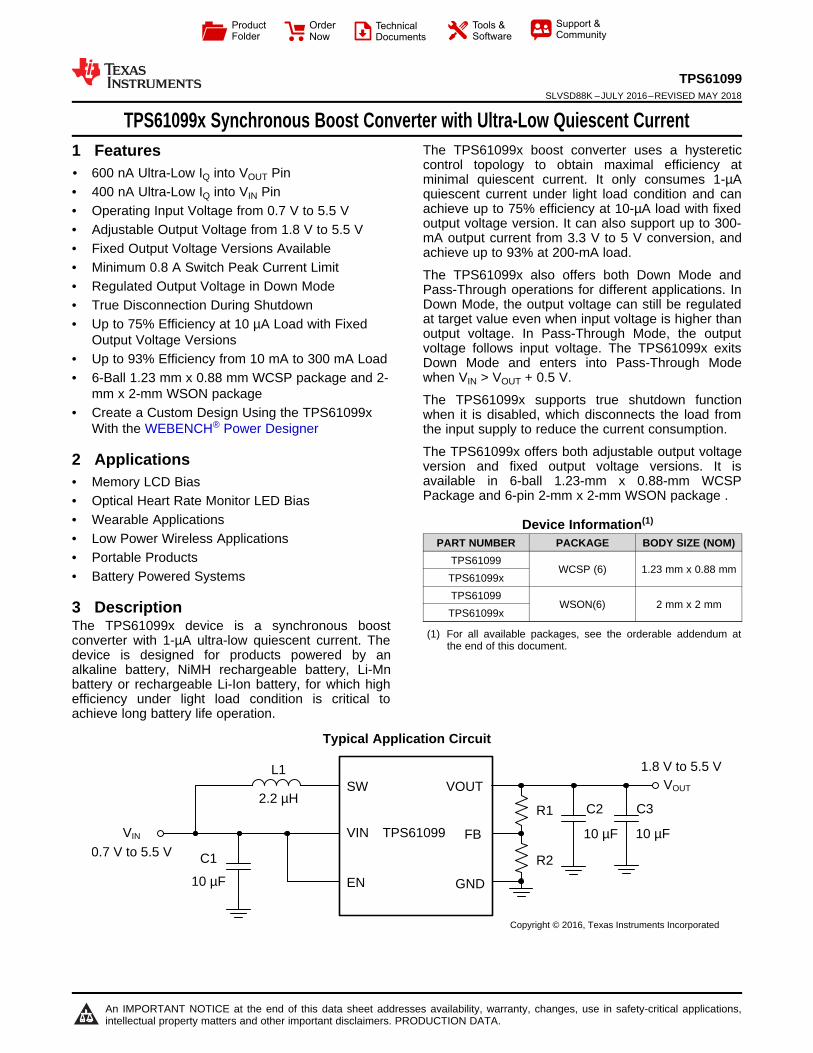
TPS61099x Synchronous Boost Converter with Ultra-Low Quiescent Current
1
1 Features1• 600 nA Ultra-Low IQ into VOUT Pin• 400 nA Ultra-Low IQ into VIN Pin• Operating Input Voltage from 0.7 V to 5.5 V• Adjustable Output Voltage from 1.8 V to 5.5 V• Fixed Output Voltage Versions Available• Minimum 0.8 A Switch Peak Current Limit• Regulated Output Voltage in Down Mode• True Disconnection During Shutdown• Up to 75% Efficiency at 10 µA Load with Fixed
Output Voltage Versions• Up to 93% Efficiency from 10 mA to 300 mA Load• 6-Ball 1.23 mm x 0.88 mm WCSP package and 2-
mm x 2-mm WSON package• Create a Custom Design Using the TPS61099x
With the WEBENCH® Power Designer
2 Applications• Memory LCD Bias• Optical Heart Rate Monitor LED Bias• Wearable Applications• Low Power Wireless Applications• Portable Products• Battery Powered Systems
3 DescriptionThe TPS61099x device is a synchronous boostconverter with 1-µA ultra-low quiescent current. Thedevice is designed for products powered by analkaline battery, NiMH rechargeable battery, Li-Mnbattery or rechargeable Li-Ion battery, for which highefficiency under light load condition is critical toachieve long battery life operation.
The TPS61099x boost converter uses a hystereticcontrol topology to obtain maximal efficiency atminimal quiescent current. It only consumes 1-µAquiescent current under light load condition and canachieve up to 75% efficiency at 10-µA load with fixedoutput voltage version. It can also support up to 300-mA output current from 3.3 V to 5 V conversion, andachieve up to 93% at 200-mA load.
The TPS61099x also offers both Down Mode andPass-Through operations for different applications. InDown Mode, the output voltage can still be regulatedat target value even when input voltage is higher thanoutput voltage. In Pass-Through Mode, the outputvoltage follows input voltage. The TPS61099x exitsDown Mode and enters into Pass-Through Modewhen VIN > VOUT + 0.5 V.
The TPS61099x supports true shutdown functionwhen it is disabled, which disconnects the load fromthe input supply to reduce the current consumption.
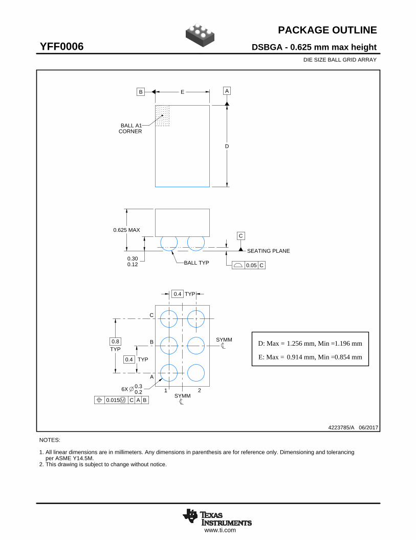
The TPS61099x offers both adjustable output voltageversion and fixed output voltage versions. It isavailable in 6-ball 1.23-mm x 0.88-mm WCSPPackage and 6-pin 2-mm x 2-mm WSON package .
Device Information(1)
PART NUMBER PACKAGE BODY SIZE (NOM)TPS61099
WCSP (6) 1.23 mm x 0.88 mmTPS61099xTPS61099
WSON(6) 2 mm x 2 mmTPS61099x
(1) For all available packages, see the orderable addendum atthe end of this document.
Typical Application Circuit
2
TPS61099SLVSD88K –JULY 2016–REVISED MAY 2018 www.ti.com
Product Folder Links: TPS61099
Submit Documentation Feedback Copyright © 2016–2018, Texas Instruments Incorporated
Table of Contents1 Features .................................................................. 12 Applications ........................................................... 13 Description ............................................................. 14 Revision History..................................................... 25 Device Comparison Table ..................................... 46 Pin Configuration and Functions ......................... 47 Specifications......................................................... 5
7.1 Absolute Maximum Ratings ...................................... 57.2 ESD Ratings.............................................................. 57.3 Recommended Operating Conditions....................... 57.4 Thermal Information .................................................. 57.5 Electrical Characteristics........................................... 67.6 Typical Characteristics .............................................. 8
8 Detailed Description ............................................ 118.1 Overview ................................................................. 118.2 Functional Block Diagram ....................................... 118.3 Feature Description................................................. 11
8.4 Device Functional Modes........................................ 149 Application and Implementation ........................ 15
9.1 Application Information............................................ 159.2 Typical Application - 5 V Output Boost Converter .. 15
10 Power Supply Recommendations ..................... 1911 Layout................................................................... 20
11.1 Layout Guidelines ................................................. 2011.2 Layout Example .................................................... 20
12 Device and Documentation Support ................. 2212.1 Device Support...................................................... 2212.2 Documentation Support ........................................ 2212.3 Receiving Notification of Documentation Updates 2212.4 Community Resources.......................................... 2212.5 Trademarks ........................................................... 2312.6 Electrostatic Discharge Caution............................ 2312.7 Glossary ................................................................ 23
13 Mechanical, Packaging, and OrderableInformation ........................................................... 23
4 Revision HistoryNOTE: Page numbers for previous revisions may differ from page numbers in the current version.
Changes from Revision J (October 2017) to Revision K Page
• Added Load Efficiency graph for TPS610995 device ............................................................................................................ 8
Changes from Revision I (September 2017) to Revision J Page
• Changed from +0.3 V to +0.5 V in Description section .......................................................................................................... 1• Changed graph image for Figure 7 ........................................................................................................................................ 8• Changed from +0.3 V to +0.5 V in fourth paragraph of Down Mode Regulation and Pass-Through Operation section ..... 13• Changed Image for Figure 20 ............................................................................................................................................. 14
Changes from Revision H (July 2017) to Revision I Page
• Added devices to the Device Comparison Table and added graphs to Typical Characteristics section. .............................. 4
Changes from Revision G (July 2017) to Revision H Page
• Changed TPS610994 Output accuracy typical value from 3.33 to 3.4 for "VIN < VOUT, PFM mode" in the ElectricalCharacteristics table. .............................................................................................................................................................. 6
• Changed TPS610993 Output accuracy typical value from 3.03 to 3.1 for "VIN < VOUT, PFM mode" in the ElectricalCharacteristics table. .............................................................................................................................................................. 6
Changes from Revision F (June 2017) to Revision G Page
• Added TPS610993 device Output accuracy specs. to Electrical Characteristics table ........................................................ 6
3
TPS61099www.ti.com SLVSD88K –JULY 2016–REVISED MAY 2018
Product Folder Links: TPS61099
Submit Documentation FeedbackCopyright © 2016–2018, Texas Instruments Incorporated
Changes from Revision E (April 2017) to Revision F Page
• Deleted voltage-variant devices from Data Sheet Header .................................................................................................... 1• Added TPS610993 Load Efficiency with Different Inputs....................................................................................................... 8• Changed Functional Block Diagram .................................................................................................................................... 11
Changes from Revision D (March 2017) to Revision E Page
• Changed figures 1 and 2: Load Efficiency with Different Inputs, figure 3:TPS610994 Load Efficiency with DifferentInputs, and figure 4:Load Efficiency with Different Outputs with new graph data .................................................................. 8
Changes from Revision C (January 2017) to Revision D Page
• Changed text string in the Programming the Output Voltage section, 2nd para From "....the FB pin should beconnected to the VOUT pin directly" To ".....the FB pin should be connected to the GND" .................................................. 16
Changes from Revision B (December 2016) to Revision C Page
• Added WEBENCH® Model ..................................................................................................................................................... 1• Added devices to the Device Comparison Table .................................................................................................................. 4• Added TPS610994 device Output accuracy specs. to Electrical Characteristics table ........................................................ 6• Added Figure 5 ...................................................................................................................................................................... 8• Added Figure 15 .................................................................................................................................................................... 9
Changes from Revision A (September 2016) to Revision B Page
• Added device TPS610997; global change ............................................................................................................................ 1• Changed From: "Connect to VOUT pin...." To: " Connect to GND pin...." for C2 pin description in the Pin
Configuration and Functions table, . ...................................................................................................................................... 4• Added Output accuracy spec for TPS610997 device in the Output section of the Electrical Characteristics table .............. 6• Added Figure 2 and Figure 14................................................................................................................................................ 9
Changes from Original (June 2016) to Revision A Page
• Added full data sheet specs - global change ........................................................................................................................ 1
2
3
6
5
4
1 Pow
erPad
A1 A2
B1 B2
C1 C2
VIN
SW
EN
GND
VOUT
FB
4
TPS61099SLVSD88K –JULY 2016–REVISED MAY 2018 www.ti.com
Product Folder Links: TPS61099
Submit Documentation Feedback Copyright © 2016–2018, Texas Instruments Incorporated
(1) Product Preview. Contact TI factory for more information.
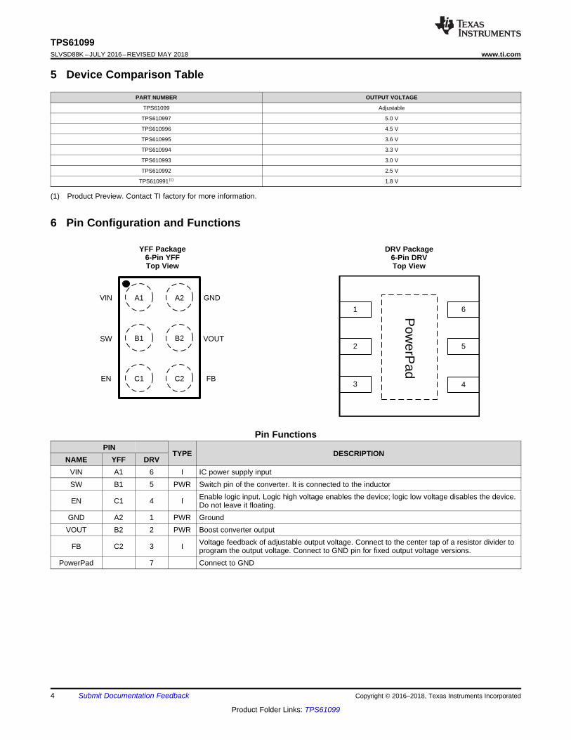
5 Device Comparison Table
PART NUMBER OUTPUT VOLTAGE
TPS61099 Adjustable
TPS610997 5.0 V
TPS610996 4.5 V
TPS610995 3.6 V
TPS610994 3.3 V
TPS610993 3.0 V
TPS610992 2.5 V
TPS610991 (1) 1.8 V
6 Pin Configuration and Functions
YFF Package6-Pin YFFTop View
DRV Package6-Pin DRVTop View
Pin FunctionsPIN
TYPE DESCRIPTIONNAME YFF DRV
VIN A1 6 I IC power supply inputSW B1 5 PWR Switch pin of the converter. It is connected to the inductor
EN C1 4 I Enable logic input. Logic high voltage enables the device; logic low voltage disables the device.Do not leave it floating.
GND A2 1 PWR GroundVOUT B2 2 PWR Boost converter output
FB C2 3 I Voltage feedback of adjustable output voltage. Connect to the center tap of a resistor divider toprogram the output voltage. Connect to GND pin for fixed output voltage versions.
PowerPad 7 Connect to GND
5
TPS61099www.ti.com SLVSD88K –JULY 2016–REVISED MAY 2018
Product Folder Links: TPS61099
Submit Documentation FeedbackCopyright © 2016–2018, Texas Instruments Incorporated
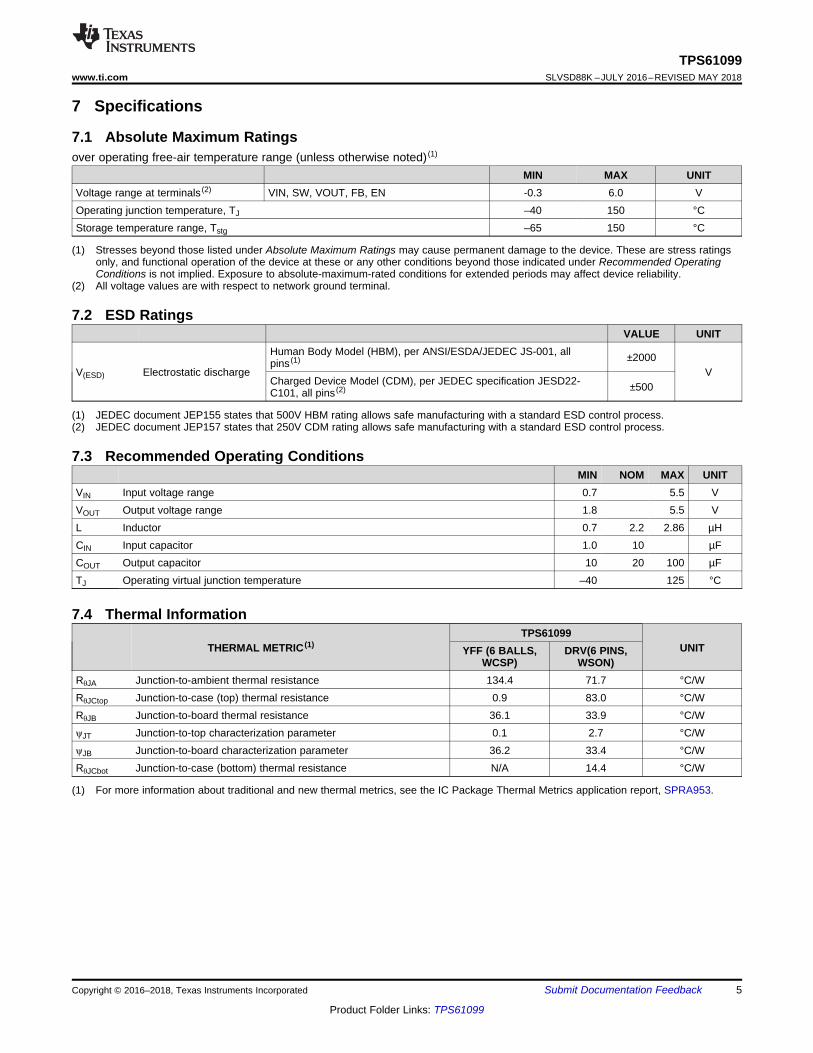
(1) Stresses beyond those listed under Absolute Maximum Ratings may cause permanent damage to the device. These are stress ratingsonly, and functional operation of the device at these or any other conditions beyond those indicated under Recommended OperatingConditions is not implied. Exposure to absolute-maximum-rated conditions for extended periods may affect device reliability.
(2) All voltage values are with respect to network ground terminal.
7 Specifications
7.1 Absolute Maximum Ratingsover operating free-air temperature range (unless otherwise noted) (1)
MIN MAX UNITVoltage range at terminals (2) VIN, SW, VOUT, FB, EN -0.3 6.0 VOperating junction temperature, TJ –40 150 °CStorage temperature range, Tstg –65 150 °C
(1) JEDEC document JEP155 states that 500V HBM rating allows safe manufacturing with a standard ESD control process.(2) JEDEC document JEP157 states that 250V CDM rating allows safe manufacturing with a standard ESD control process.
7.2 ESD RatingsVALUE UNIT
V(ESD) Electrostatic discharge
Human Body Model (HBM), per ANSI/ESDA/JEDEC JS-001, allpins (1) ±2000
VCharged Device Model (CDM), per JEDEC specification JESD22-C101, all pins (2) ±500
7.3 Recommended Operating ConditionsMIN NOM MAX UNIT
VIN Input voltage range 0.7 5.5 VVOUT Output voltage range 1.8 5.5 VL Inductor 0.7 2.2 2.86 µHCIN Input capacitor 1.0 10 µFCOUT Output capacitor 10 20 100 µFTJ Operating virtual junction temperature –40 125 °C
(1) For more information about traditional and new thermal metrics, see the IC Package Thermal Metrics application report, SPRA953.
7.4 Thermal Information
THERMAL METRIC (1)TPS61099
UNITYFF (6 BALLS,WCSP)
DRV(6 PINS,WSON)
RθJA Junction-to-ambient thermal resistance 134.4 71.7 °C/WRθJCtop Junction-to-case (top) thermal resistance 0.9 83.0 °C/WRθJB Junction-to-board thermal resistance 36.1 33.9 °C/WψJT Junction-to-top characterization parameter 0.1 2.7 °C/WψJB Junction-to-board characterization parameter 36.2 33.4 °C/WRθJCbot Junction-to-case (bottom) thermal resistance N/A 14.4 °C/W
6
TPS61099SLVSD88K –JULY 2016–REVISED MAY 2018 www.ti.com
Product Folder Links: TPS61099
Submit Documentation Feedback Copyright © 2016–2018, Texas Instruments Incorporated
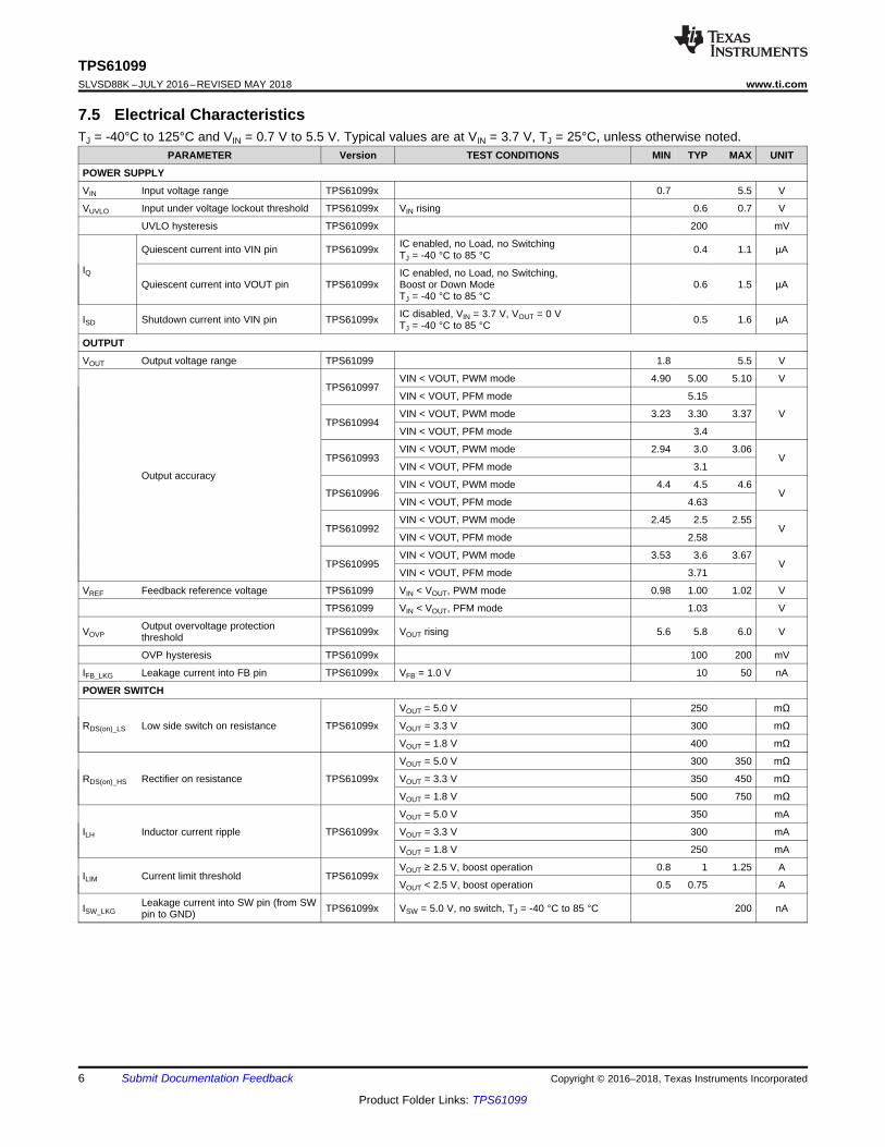
7.5 Electrical CharacteristicsTJ = -40°C to 125°C and VIN = 0.7 V to 5.5 V. Typical values are at VIN = 3.7 V, TJ = 25°C, unless otherwise noted.
PARAMETER Version TEST CONDITIONS MIN TYP MAX UNIT
POWER SUPPLY
VIN Input voltage range TPS61099x 0.7 5.5 V
VUVLO Input under voltage lockout threshold TPS61099x VIN rising 0.6 0.7 V
UVLO hysteresis TPS61099x 200 mV
IQ
Quiescent current into VIN pin TPS61099x IC enabled, no Load, no SwitchingTJ = -40 °C to 85 °C 0.4 1.1 µA
Quiescent current into VOUT pin TPS61099xIC enabled, no Load, no Switching,Boost or Down ModeTJ = -40 °C to 85 °C
0.6 1.5 µA
ISD Shutdown current into VIN pin TPS61099x IC disabled, VIN = 3.7 V, VOUT = 0 VTJ = -40 °C to 85 °C 0.5 1.6 µA
OUTPUT
VOUT Output voltage range TPS61099 1.8 5.5 V
Output accuracy
TPS610997VIN < VOUT, PWM mode 4.90 5.00 5.10 V
VIN < VOUT, PFM mode 5.15
VTPS610994
VIN < VOUT, PWM mode 3.23 3.30 3.37
VIN < VOUT, PFM mode 3.4
TPS610993VIN < VOUT, PWM mode 2.94 3.0 3.06
VVIN < VOUT, PFM mode 3.1
TPS610996VIN < VOUT, PWM mode 4.4 4.5 4.6
VVIN < VOUT, PFM mode 4.63
TPS610992VIN < VOUT, PWM mode 2.45 2.5 2.55
VVIN < VOUT, PFM mode 2.58
TPS610995VIN < VOUT, PWM mode 3.53 3.6 3.67
VVIN < VOUT, PFM mode 3.71
VREF Feedback reference voltage TPS61099 VIN < VOUT, PWM mode 0.98 1.00 1.02 V
TPS61099 VIN < VOUT, PFM mode 1.03 V
VOVPOutput overvoltage protectionthreshold TPS61099x VOUT rising 5.6 5.8 6.0 V
OVP hysteresis TPS61099x 100 200 mV
IFB_LKG Leakage current into FB pin TPS61099x VFB = 1.0 V 10 50 nA
POWER SWITCH
RDS(on)_LS Low side switch on resistance TPS61099x
VOUT = 5.0 V 250 mΩ
VOUT = 3.3 V 300 mΩ
VOUT = 1.8 V 400 mΩ
RDS(on)_HS Rectifier on resistance TPS61099x
VOUT = 5.0 V 300 350 mΩ
VOUT = 3.3 V 350 450 mΩ
VOUT = 1.8 V 500 750 mΩ
ILH Inductor current ripple TPS61099x
VOUT = 5.0 V 350 mA
VOUT = 3.3 V 300 mA
VOUT = 1.8 V 250 mA
ILIM Current limit threshold TPS61099xVOUT ≥ 2.5 V, boost operation 0.8 1 1.25 A
VOUT < 2.5 V, boost operation 0.5 0.75 A
ISW_LKGLeakage current into SW pin (from SWpin to GND) TPS61099x VSW = 5.0 V, no switch, TJ = -40 °C to 85 °C 200 nA
7
TPS61099www.ti.com SLVSD88K –JULY 2016–REVISED MAY 2018
Product Folder Links: TPS61099
Submit Documentation FeedbackCopyright © 2016–2018, Texas Instruments Incorporated
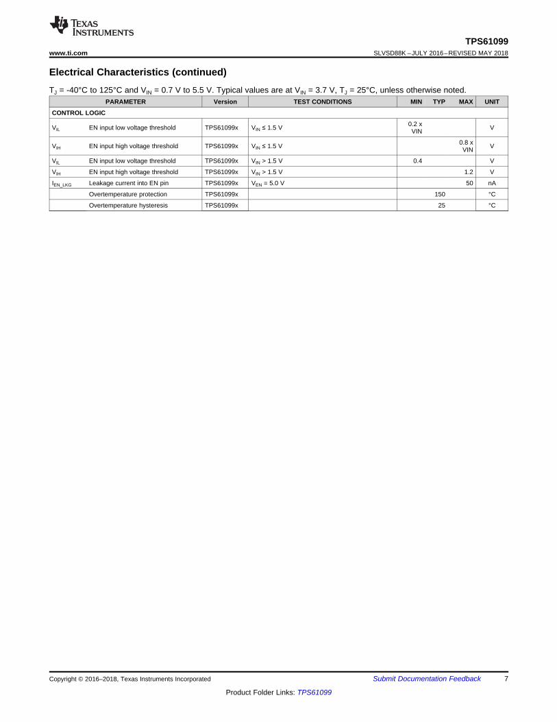
Electrical Characteristics (continued)TJ = -40°C to 125°C and VIN = 0.7 V to 5.5 V. Typical values are at VIN = 3.7 V, TJ = 25°C, unless otherwise noted.
PARAMETER Version TEST CONDITIONS MIN TYP MAX UNIT
CONTROL LOGIC
VIL EN input low voltage threshold TPS61099x VIN ≤ 1.5 V 0.2 xVIN V
VIH EN input high voltage threshold TPS61099x VIN ≤ 1.5 V 0.8 xVIN V
VIL EN input low voltage threshold TPS61099x VIN > 1.5 V 0.4 V
VIH EN input high voltage threshold TPS61099x VIN > 1.5 V 1.2 V
IEN_LKG Leakage current into EN pin TPS61099x VEN = 5.0 V 50 nA
Overtemperature protection TPS61099x 150 °C
Overtemperature hysteresis TPS61099x 25 °C
IOUT (mA)
Load
Effi
cien
cy w
ith D
iffer
ent I
nput
0.005 0.1 1 10 100 100060
65
70
75
80
85
90
95
100
D003
VIN = 0.7 VVIN = 1.5 VVIN = 2.5 VVIN = 3.0 V
1 10 100 10000.1I (mA)OUT
Iout (mA)
Effi
cien
cy (
%)
0.01 0.1 0.2 0.5 1 2 3 5 710 20 50 100 100050
55
60
65
70
75
80
85
90
95
100
TPS6
VIN = 0.7VVIN = 1.5VVIN = 2.5VVIN = 3.0VVIN = 3.3V
Output Current (mA)
Effi
cien
cy (
%)
50
55
60
65
70
75
80
85
90
95
100
0.01 0.1 1 10 100 1000
D016
VIN = 0.7 VVIN = 1.5 VVIN = 2.7 V
VIN = 3.3 VVIN = 4.2 V
IOUT (mA)
Load
Effi
cien
cy w
ith D
iffer
ent I
nput
0.005 0.1 1 10 100 100045
50
55
60
65
70
75
80
85
90
95
100
D001
VIN = 0.7 VVIN = 1.5 VVIN = 3.0 VVIN = 3.6 VVIN = 4.2 V
IOUT (mA)
Load
Effi
cien
cy w
ith D
iffer
ent I
nput
0.005 0.1 1 10 100 100055
60
65
70
75
80
85
90
95
100
D002
VIN = 0.7 VVIN = 1.5 VVIN = 3.0 VVIN = 3.6 VVIN = 4.2 V
8
TPS61099SLVSD88K –JULY 2016–REVISED MAY 2018 www.ti.com
Product Folder Links: TPS61099
Submit Documentation Feedback Copyright © 2016–2018, Texas Instruments Incorporated
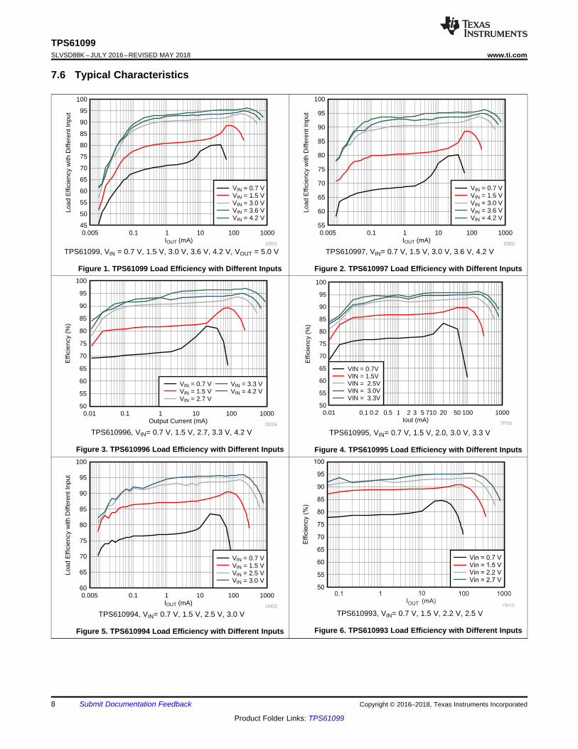
7.6 Typical Characteristics
TPS61099, VIN = 0.7 V, 1.5 V, 3.0 V, 3.6 V, 4.2 V, VOUT = 5.0 V
Figure 1. TPS61099 Load Efficiency with Different Inputs
TPS610997, VIN= 0.7 V, 1.5 V, 3.0 V, 3.6 V, 4.2 V
Figure 2. TPS610997 Load Efficiency with Different Inputs
TPS610996, VIN= 0.7 V, 1.5 V, 2.7, 3.3 V, 4.2 V
Figure 3. TPS610996 Load Efficiency with Different Inputs
TPS610995, VIN= 0.7 V, 1.5 V, 2.0, 3.0 V, 3.3 V
Figure 4. TPS610995 Load Efficiency with Different Inputs
TPS610994, VIN= 0.7 V, 1.5 V, 2.5 V, 3.0 V
Figure 5. TPS610994 Load Efficiency with Different Inputs
TPS610993, VIN= 0.7 V, 1.5 V, 2.2 V, 2.5 V
Figure 6. TPS610993 Load Efficiency with Different Inputs
Temperature (°C)
Quie
scentC
urr
ent(µ
A)
-40 -20 0 20 40 60 80 1000.1
0.2
0.3
0.4
0.5
0.6
0.7
D005
VIN = 3.7 V
Temperature (°C)
Sh
utd
ow
n C
urr
en
t(µ
A)
-40 -20 0 20 40 60 80 1000
0.2
0.4
0.6
0.8
1
1.2
D006
VIN = 3.7 V
Temperature (°C)
Qu
iesce
ntC
urr
en
t(µ
A)
-40 -20 0 20 40 60 80 1000
0.2
0.4
0.6
0.8
1
1.2
D004
VIN = 3.7 V
4.7
4.8
4.9
5
5.1
5.2
5.3
5.4
10 µ
Ou
tpu
t V
olt
ag
e (
V)
Output Current (A)
1 m100 µ 600 m10 m 100 m
Vin = 0.7 V
Vin = 1.5 V
Vin = 3.0 V
Vin = 3.6 V
Vin = 4.2 V
D003a
IOUT (mA)
Load
Effi
cien
cy w
ith D
iffer
ent O
utpu
t
0.005 0.1 1 10 100 100050
55
60
65
70
75
80
85
90
95
D004
VOUT = 3.0 VVOUT = 3.6 VVOUT = 4.5 VVOUT = 5.0 V
Output Current (mA)
Effi
cien
cy (
%)
50
55
60
65
70
75
80
85
90
95
100
0.01 0.1 1 10 100 1000
D014
VIN = 0.7 VVIN = 1.2 VVIN = 1.5 VVIN = 2.2 V
9
TPS61099www.ti.com SLVSD88K –JULY 2016–REVISED MAY 2018
Product Folder Links: TPS61099
Submit Documentation FeedbackCopyright © 2016–2018, Texas Instruments Incorporated
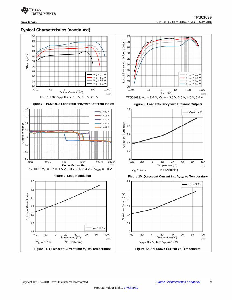
Typical Characteristics (continued)
TPS610992, VIN= 0.7 V, 1.2 V, 1.5 V, 2.2 V
Figure 7. TPS610992 Load Efficiency with Different Inputs
TPS61099, VIN = 2.4 V, VOUT = 3.0 V, 3.6 V, 4.5 V, 5.0 V
Figure 8. Load Efficiency with Different Outputs
TPS61099, VIN = 0.7 V, 1.5 V, 3.0 V, 3.6 V, 4.2 V, VOUT = 5.0 V
Figure 9. Load Regulation
VIN = 3.7 V No Switching
Figure 10. Quiescent Current into VOUT vs Temperature
VIN = 3.7 V No Switching
Figure 11. Quiescent Current into VIN vs Temperature
VIN = 3.7 V, Into VIN and SW
Figure 12. Shutdown Current vs Temperature
Temperature (°C)
Curr
entLim
it(A
)
–40 10 60 125
0.9
0.95
1
1.05
1.1
D001
VIN = 3.7 V
Temperature (qC)
Out
put V
olta
ge (
V)
-40 -20 0 20 40 60 80 100 120 1403.304
3.306
3.308
3.31
3.312
3.314
3.316
3.318
3.32
3.322
3.324
D012
Temperature (qC)
Out
put V
olta
ge (
V)
-40 -20 0 20 40 60 80 100 120 1405
5.002
5.004
5.006
5.008
5.01
5.012
5.014
5.016
5.018
5.02
D010Temperature (°C)
Refe
ren
ce
Voltage
(V)
-40 -20 0 20 40 60 80 100 120 1400.995
0.997
0.999
1.001
1.003
1.005
1.007
1.009VIN = 3.7 V
10
TPS61099SLVSD88K –JULY 2016–REVISED MAY 2018 www.ti.com
Product Folder Links: TPS61099
Submit Documentation Feedback Copyright © 2016–2018, Texas Instruments Incorporated
Typical Characteristics (continued)
TPS61099, VIN = 3.7 V TJ = –40°C to 125°C
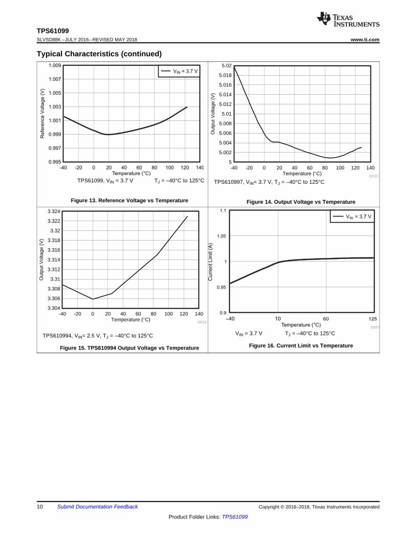
Figure 13. Reference Voltage vs Temperature
TPS610997, VIN= 3.7 V, TJ = –40°C to 125°C
Figure 14. Output Voltage vs Temperature
TPS610994, VIN= 2.5 V, TJ = –40°C to 125°C
Figure 15. TPS610994 Output Voltage vs Temperature
VIN = 3.7 V TJ = –40°C to 125°C
Figure 16. Current Limit vs Temperature
Current SenseBoost
Gate Driver
Pulse Modulator
B2B1
A1
Logic Control
C1
REF
SW
EN
VOUT
VIN
Pass-Through
VPSTH
C2
TPS61099 x
TPS61099
(1)
Thermal Shutdown
OCP
UVLO
Down ModeVDOWN
Startup
Protection(OCP, OVP)
OVP
A2
FB
GND
Copyright © 2017, Texas Instruments Incorporated
11
TPS61099www.ti.com SLVSD88K –JULY 2016–REVISED MAY 2018
Product Folder Links: TPS61099
Submit Documentation FeedbackCopyright © 2016–2018, Texas Instruments Incorporated
8 Detailed Description
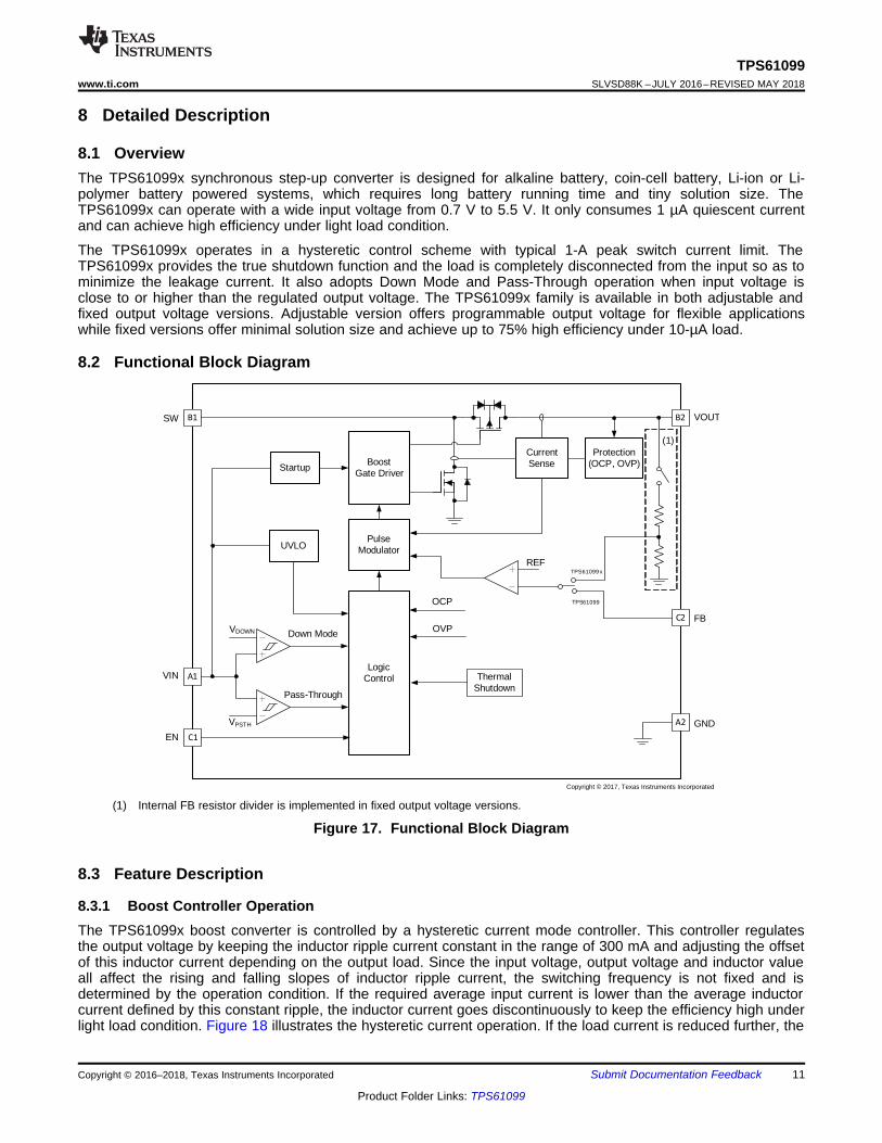
8.1 OverviewThe TPS61099x synchronous step-up converter is designed for alkaline battery, coin-cell battery, Li-ion or Li-polymer battery powered systems, which requires long battery running time and tiny solution size. TheTPS61099x can operate with a wide input voltage from 0.7 V to 5.5 V. It only consumes 1 µA quiescent currentand can achieve high efficiency under light load condition.
The TPS61099x operates in a hysteretic control scheme with typical 1-A peak switch current limit. TheTPS61099x provides the true shutdown function and the load is completely disconnected from the input so as tominimize the leakage current. It also adopts Down Mode and Pass-Through operation when input voltage isclose to or higher than the regulated output voltage. The TPS61099x family is available in both adjustable andfixed output voltage versions. Adjustable version offers programmable output voltage for flexible applicationswhile fixed versions offer minimal solution size and achieve up to 75% high efficiency under 10-µA load.
8.2 Functional Block Diagram
(1) Internal FB resistor divider is implemented in fixed output voltage versions.
Figure 17. Functional Block Diagram
8.3 Feature Description
8.3.1 Boost Controller OperationThe TPS61099x boost converter is controlled by a hysteretic current mode controller. This controller regulatesthe output voltage by keeping the inductor ripple current constant in the range of 300 mA and adjusting the offsetof this inductor current depending on the output load. Since the input voltage, output voltage and inductor valueall affect the rising and falling slopes of inductor ripple current, the switching frequency is not fixed and isdetermined by the operation condition. If the required average input current is lower than the average inductorcurrent defined by this constant ripple, the inductor current goes discontinuously to keep the efficiency high underlight load condition. Figure 18 illustrates the hysteretic current operation. If the load current is reduced further, the
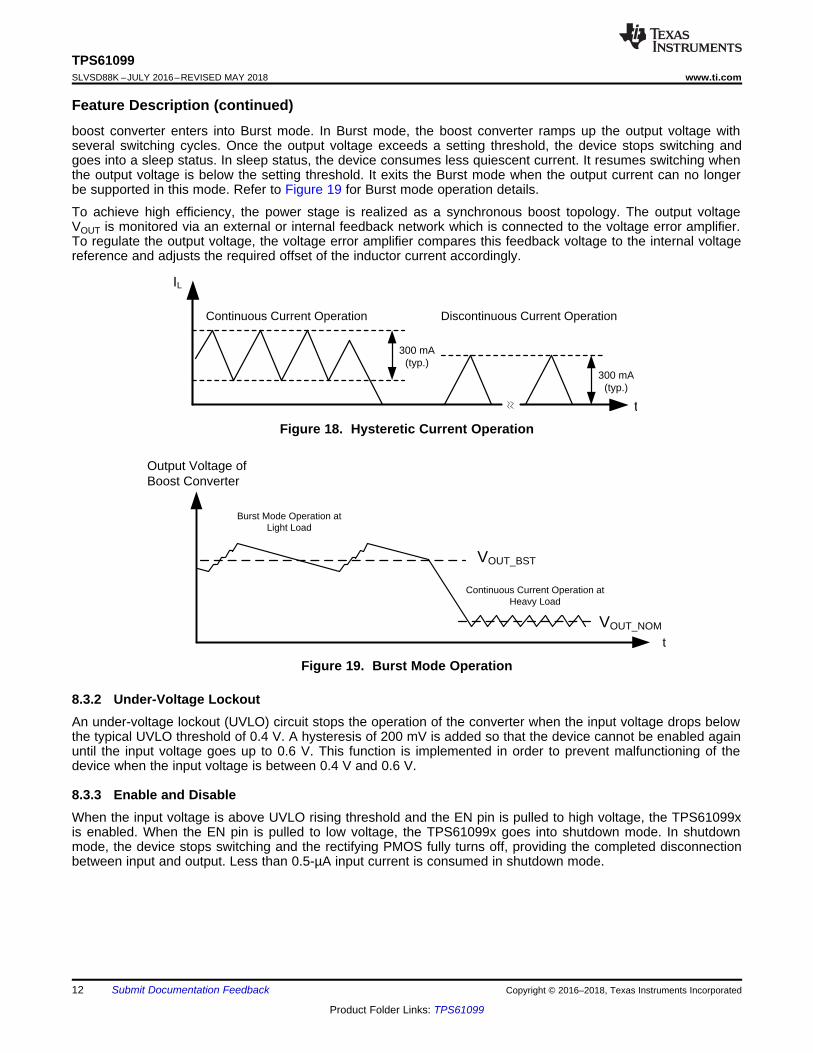
Continuous Current Operation at Heavy Load
Burst Mode Operation at Light Load
Output Voltage of Boost Converter
t
VOUT_NOM
VOUT_BST
Continuous Current Operation
300 mA(typ.)
300 mA(typ.)
Discontinuous Current Operation
IL
t
12
TPS61099SLVSD88K –JULY 2016–REVISED MAY 2018 www.ti.com
Product Folder Links: TPS61099
Submit Documentation Feedback Copyright © 2016–2018, Texas Instruments Incorporated
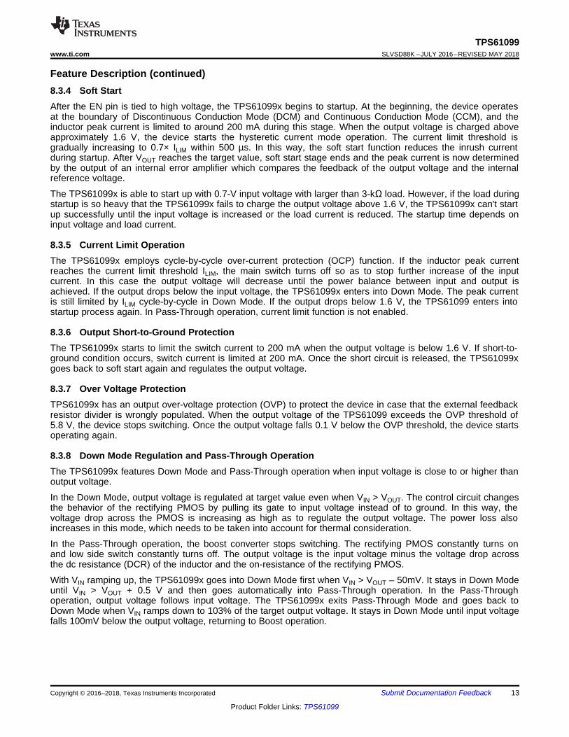
Feature Description (continued)boost converter enters into Burst mode. In Burst mode, the boost converter ramps up the output voltage withseveral switching cycles. Once the output voltage exceeds a setting threshold, the device stops switching andgoes into a sleep status. In sleep status, the device consumes less quiescent current. It resumes switching whenthe output voltage is below the setting threshold. It exits the Burst mode when the output current can no longerbe supported in this mode. Refer to Figure 19 for Burst mode operation details.
To achieve high efficiency, the power stage is realized as a synchronous boost topology. The output voltageVOUT is monitored via an external or internal feedback network which is connected to the voltage error amplifier.To regulate the output voltage, the voltage error amplifier compares this feedback voltage to the internal voltagereference and adjusts the required offset of the inductor current accordingly.
Figure 18. Hysteretic Current Operation
Figure 19. Burst Mode Operation
8.3.2 Under-Voltage LockoutAn under-voltage lockout (UVLO) circuit stops the operation of the converter when the input voltage drops belowthe typical UVLO threshold of 0.4 V. A hysteresis of 200 mV is added so that the device cannot be enabled againuntil the input voltage goes up to 0.6 V. This function is implemented in order to prevent malfunctioning of thedevice when the input voltage is between 0.4 V and 0.6 V.
8.3.3 Enable and DisableWhen the input voltage is above UVLO rising threshold and the EN pin is pulled to high voltage, the TPS61099xis enabled. When the EN pin is pulled to low voltage, the TPS61099x goes into shutdown mode. In shutdownmode, the device stops switching and the rectifying PMOS fully turns off, providing the completed disconnectionbetween input and output. Less than 0.5-µA input current is consumed in shutdown mode.
13
TPS61099www.ti.com SLVSD88K –JULY 2016–REVISED MAY 2018
Product Folder Links: TPS61099
Submit Documentation FeedbackCopyright © 2016–2018, Texas Instruments Incorporated
Feature Description (continued)8.3.4 Soft StartAfter the EN pin is tied to high voltage, the TPS61099x begins to startup. At the beginning, the device operatesat the boundary of Discontinuous Conduction Mode (DCM) and Continuous Conduction Mode (CCM), and theinductor peak current is limited to around 200 mA during this stage. When the output voltage is charged aboveapproximately 1.6 V, the device starts the hysteretic current mode operation. The current limit threshold isgradually increasing to 0.7× ILIM within 500 µs. In this way, the soft start function reduces the inrush currentduring startup. After VOUT reaches the target value, soft start stage ends and the peak current is now determinedby the output of an internal error amplifier which compares the feedback of the output voltage and the internalreference voltage.
The TPS61099x is able to start up with 0.7-V input voltage with larger than 3-kΩ load. However, if the load duringstartup is so heavy that the TPS61099x fails to charge the output voltage above 1.6 V, the TPS61099x can't startup successfully until the input voltage is increased or the load current is reduced. The startup time depends oninput voltage and load current.
8.3.5 Current Limit OperationThe TPS61099x employs cycle-by-cycle over-current protection (OCP) function. If the inductor peak currentreaches the current limit threshold ILIM, the main switch turns off so as to stop further increase of the inputcurrent. In this case the output voltage will decrease until the power balance between input and output isachieved. If the output drops below the input voltage, the TPS61099x enters into Down Mode. The peak currentis still limited by ILIM cycle-by-cycle in Down Mode. If the output drops below 1.6 V, the TPS61099 enters intostartup process again. In Pass-Through operation, current limit function is not enabled.
8.3.6 Output Short-to-Ground ProtectionThe TPS61099x starts to limit the switch current to 200 mA when the output voltage is below 1.6 V. If short-to-ground condition occurs, switch current is limited at 200 mA. Once the short circuit is released, the TPS61099xgoes back to soft start again and regulates the output voltage.
8.3.7 Over Voltage ProtectionTPS61099x has an output over-voltage protection (OVP) to protect the device in case that the external feedbackresistor divider is wrongly populated. When the output voltage of the TPS61099 exceeds the OVP threshold of5.8 V, the device stops switching. Once the output voltage falls 0.1 V below the OVP threshold, the device startsoperating again.
8.3.8 Down Mode Regulation and Pass-Through OperationThe TPS61099x features Down Mode and Pass-Through operation when input voltage is close to or higher thanoutput voltage.
In the Down Mode, output voltage is regulated at target value even when VIN > VOUT. The control circuit changesthe behavior of the rectifying PMOS by pulling its gate to input voltage instead of to ground. In this way, thevoltage drop across the PMOS is increasing as high as to regulate the output voltage. The power loss alsoincreases in this mode, which needs to be taken into account for thermal consideration.
In the Pass-Through operation, the boost converter stops switching. The rectifying PMOS constantly turns onand low side switch constantly turns off. The output voltage is the input voltage minus the voltage drop acrossthe dc resistance (DCR) of the inductor and the on-resistance of the rectifying PMOS.
With VIN ramping up, the TPS61099x goes into Down Mode first when VIN > VOUT – 50mV. It stays in Down Modeuntil VIN > VOUT + 0.5 V and then goes automatically into Pass-Through operation. In the Pass-Throughoperation, output voltage follows input voltage. The TPS61099x exits Pass-Through Mode and goes back toDown Mode when VIN ramps down to 103% of the target output voltage. It stays in Down Mode until input voltagefalls 100mV below the output voltage, returning to Boost operation.
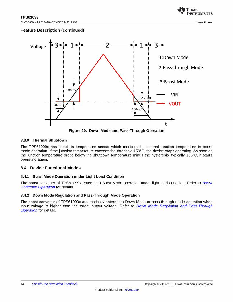
1 12 33
1:Down Mode
2:Pass-through Mode
3:Boost Mode
VIN
VOUT
t
Voltage
50mV
500mV
3%*VOUT
100mV
14
TPS61099SLVSD88K –JULY 2016–REVISED MAY 2018 www.ti.com
Product Folder Links: TPS61099
Submit Documentation Feedback Copyright © 2016–2018, Texas Instruments Incorporated
Feature Description (continued)
Figure 20. Down Mode and Pass-Through Operation
8.3.9 Thermal ShutdownThe TPS61099x has a built-in temperature sensor which monitors the internal junction temperature in boostmode operation. If the junction temperature exceeds the threshold 150°C, the device stops operating. As soon asthe junction temperature drops below the shutdown temperature minus the hysteresis, typically 125°C, it startsoperating again.
8.4 Device Functional Modes
8.4.1 Burst Mode Operation under Light Load ConditionThe boost converter of TPS61099x enters into Burst Mode operation under light load condition. Refer to BoostController Operation for details.
8.4.2 Down Mode Regulation and Pass-Through Mode OperationThe boost converter of TPS61099x automatically enters into Down Mode or pass-through mode operation wheninput voltage is higher than the target output voltage. Refer to Down Mode Regulation and Pass-ThroughOperation for details.
SW
VIN
EN GND
VOUT
FB
L1
2.2 µH
C1
10 µF
R1
R2
C2
10 µFVIN
2.7 V to 4.2 V
VOUT
5 V
TPS61099
C3
10 µF
Copyright © 2016, Texas Instruments Incorporated
15
TPS61099www.ti.com SLVSD88K –JULY 2016–REVISED MAY 2018
Product Folder Links: TPS61099
Submit Documentation FeedbackCopyright © 2016–2018, Texas Instruments Incorporated
9 Application and Implementation
NOTEInformation in the following applications sections is not part of the TI componentspecification, and TI does not warrant its accuracy or completeness. TI’s customers areresponsible for determining suitability of components for their purposes. Customers shouldvalidate and test their design implementation to confirm system functionality.
9.1 Application InformationThe TPS61099x is a synchronous boost converter designed to operate at a wide input voltage from 0.7 V to 5.5V with 1-A peak switch current limit. The device adopts a hysteretic control scheme so the operating frequency isnot a constant value, which varies with different input/output voltages and inductor values. It only consumes 1-µAquiescent current under light load condition. It also supports true shutdown to disconnect the load from the inputin order to minimize the leakage current. Therefore, it is very suitable for alkaline battery, coin-cell battery, Li-ionor Li-polymer battery powered systems to extend the battery running time.
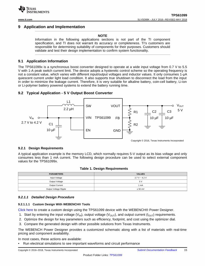
9.2 Typical Application - 5 V Output Boost Converter
9.2.1 Design RequirementsA typical application example is the memory LCD, which normally requires 5-V output as its bias voltage and onlyconsumes less than 1 mA current. The following design procedure can be used to select external componentvalues for the TPS61099x.
Table 1. Design RequirementsPARAMETERS VALUES
Input Voltage 2.7 V ~ 4.2 V
Output Voltage 5 V
Output Current 1 mA
Output Voltage Ripple ± 50 mV
9.2.1.1 Detailed Design Procedure
9.2.1.1.1 Custom Design With WEBENCH® Tools
Click here to create a custom design using the TPS61099 device with the WEBENCH® Power Designer.1. Start by entering the input voltage (VIN), output voltage (VOUT), and output current (IOUT) requirements.2. Optimize the design for key parameters such as efficiency, footprint, and cost using the optimizer dial.3. Compare the generated design with other possible solutions from Texas Instruments.
The WEBENCH Power Designer provides a customized schematic along with a list of materials with real-timepricing and component availability.
In most cases, these actions are available:• Run electrical simulations to see important waveforms and circuit performance
operation mode current ousdiscontinu ;II
operation mode current continuous ;2
IV
IVI
LHpeak,L
LH
IN
OUTOUTpeak,L
Ku
2I
V
IV LH
IN
OUTOUT !Ku
OUT
LHLIMIN
(max)OUT V
)2
II(V
IK
2R2R1R
VV REFOUT
16
TPS61099SLVSD88K –JULY 2016–REVISED MAY 2018 www.ti.com
Product Folder Links: TPS61099
Submit Documentation Feedback Copyright © 2016–2018, Texas Instruments Incorporated
• Run thermal simulations to understand board thermal performance• Export customized schematic and layout into popular CAD formats• Print PDF reports for the design, and share the design with colleagues
Get more information about WEBENCH tools at www.ti.com/WEBENCH.
9.2.1.1.2 Programming the Output Voltage
There are two ways to set the output voltage of the TPS61099x. For adjustable output voltage version, select theexternal resistor divider R1 and R2, as shown in Equation 1, the output voltage is programmed to the desiredvalue. When the output voltage is regulated, the typical voltage at the FB pin is VREF of 1.0 V.
(1)
For fixed output voltage versions, the FB pin should be connected to the GND. The TPS61099x offers diversefixed voltage versions, refer to Device Comparison Table for version details.
In this example, 5-V output is required to bias the memory LCD. For the best accuracy, the current followingthrough R2 should be 100 times larger than FB pin leakage current. Changing R2 towards a lower valueincreases the robustness against noise injection. Changing R2 towards higher values reduces the FB dividercurrent for achieving the highest efficiency at low load currents. 1-MΩ and 249-kΩ resistors are selected for R1and R2 in this example. High accuracy resistors are recommended for better output voltage accuracy.
9.2.1.1.3 Maximum Output Current
The maximum output capability of the TPS61099x is determined by the input to output ratio and the current limitof the boost converter. It can be estimated by Equation 2.
where• η is the conversion efficiency, use 85% for estimation• ILH is the current ripple value• ILIM is the switch current limit (2)
Minimum input voltage, maximum boost output voltage and minimum current limit ILIM should be used as theworst case condition for the estimation.
9.2.1.1.4 Inductor Selection
Because the selection of the inductor affects steady state operation, transient behavior, and loop stability, theinductor is the most important component in power regulator design. There are three important inductorspecifications, inductor value, saturation current, and dc resistance (DCR).
The TPS61099x is optimized to work with inductor values between 1 µH and 2.2 µH. For best stabilityconsideration, a 2.2-µH inductor is recommended under Vout > 3.0V condition while choosing a 1-µH inductor forapplications under Vout ≤ 3.0V condition. Follow Equation 3 and Equation 4 to calculate the inductor's peakcurrent for the application. Depending on different load conditions, the TPS61099x works in continuous currentmode or discontinuous mode. In different modes, the peak currents of the inductor are also different. Equation 3provides an easy way to estimate whether the device works in CCM or DCM. As long as the Equation 3 is true,continuous current mode is typically established. Otherwise, discontinuous current mode is typically established.
(3)
The inductor current ripple ILH is fixed by design. Therefore, the peak inductor current is calculated withEquation 4.
OUTLH
INOUTIN
VIL
)VV(Vf
K
17
TPS61099www.ti.com SLVSD88K –JULY 2016–REVISED MAY 2018
Product Folder Links: TPS61099
Submit Documentation FeedbackCopyright © 2016–2018, Texas Instruments Incorporated
(1) See Third-Party Products disclaimer
where• IL,peak is the peak inductor current. (4)
The inductor's saturation current must be higher than the calculated peak inductor current. Table 2 lists therecommended inductors for TPS61099x device.
After choosing the inductor, the estimated switching frequency ƒ in continuous current mode can be calculatedby Equation 5. The switching frequency is not a constant value, which is determined by L, VIN and VOUT.
(5)
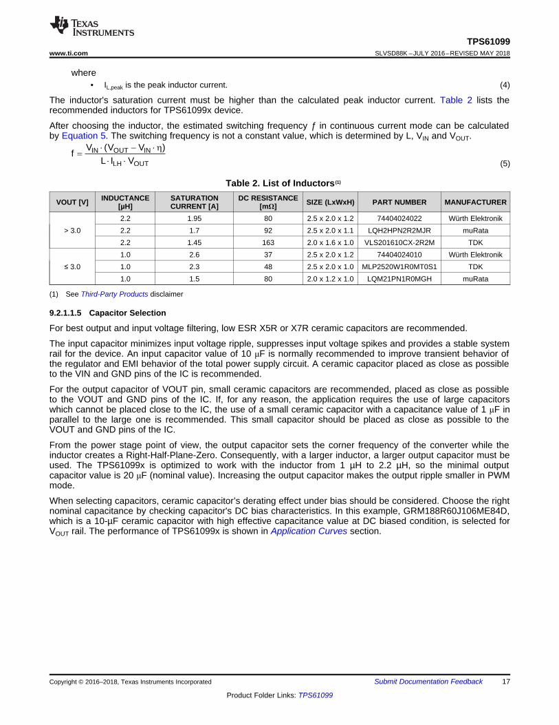
Table 2. List of Inductors (1)
VOUT [V] INDUCTANCE[µH]
SATURATIONCURRENT [A]
DC RESISTANCE[mΩ] SIZE (LxWxH) PART NUMBER MANUFACTURER
> 3.02.2 1.95 80 2.5 x 2.0 x 1.2 74404024022 Würth Elektronik2.2 1.7 92 2.5 x 2.0 x 1.1 LQH2HPN2R2MJR muRata2.2 1.45 163 2.0 x 1.6 x 1.0 VLS201610CX-2R2M TDK
≤ 3.01.0 2.6 37 2.5 x 2.0 x 1.2 74404024010 Würth Elektronik1.0 2.3 48 2.5 x 2.0 x 1.0 MLP2520W1R0MT0S1 TDK1.0 1.5 80 2.0 x 1.2 x 1.0 LQM21PN1R0MGH muRata
9.2.1.1.5 Capacitor Selection
For best output and input voltage filtering, low ESR X5R or X7R ceramic capacitors are recommended.
The input capacitor minimizes input voltage ripple, suppresses input voltage spikes and provides a stable systemrail for the device. An input capacitor value of 10 μF is normally recommended to improve transient behavior ofthe regulator and EMI behavior of the total power supply circuit. A ceramic capacitor placed as close as possibleto the VIN and GND pins of the IC is recommended.
For the output capacitor of VOUT pin, small ceramic capacitors are recommended, placed as close as possibleto the VOUT and GND pins of the IC. If, for any reason, the application requires the use of large capacitorswhich cannot be placed close to the IC, the use of a small ceramic capacitor with a capacitance value of 1 μF inparallel to the large one is recommended. This small capacitor should be placed as close as possible to theVOUT and GND pins of the IC.
From the power stage point of view, the output capacitor sets the corner frequency of the converter while theinductor creates a Right-Half-Plane-Zero. Consequently, with a larger inductor, a larger output capacitor must beused. The TPS61099x is optimized to work with the inductor from 1 µH to 2.2 µH, so the minimal outputcapacitor value is 20 μF (nominal value). Increasing the output capacitor makes the output ripple smaller in PWMmode.
When selecting capacitors, ceramic capacitor’s derating effect under bias should be considered. Choose the rightnominal capacitance by checking capacitor's DC bias characteristics. In this example, GRM188R60J106ME84D,which is a 10-µF ceramic capacitor with high effective capacitance value at DC biased condition, is selected forVOUT rail. The performance of TPS61099x is shown in Application Curves section.
18
TPS61099SLVSD88K –JULY 2016–REVISED MAY 2018 www.ti.com
Product Folder Links: TPS61099
Submit Documentation Feedback Copyright © 2016–2018, Texas Instruments Incorporated
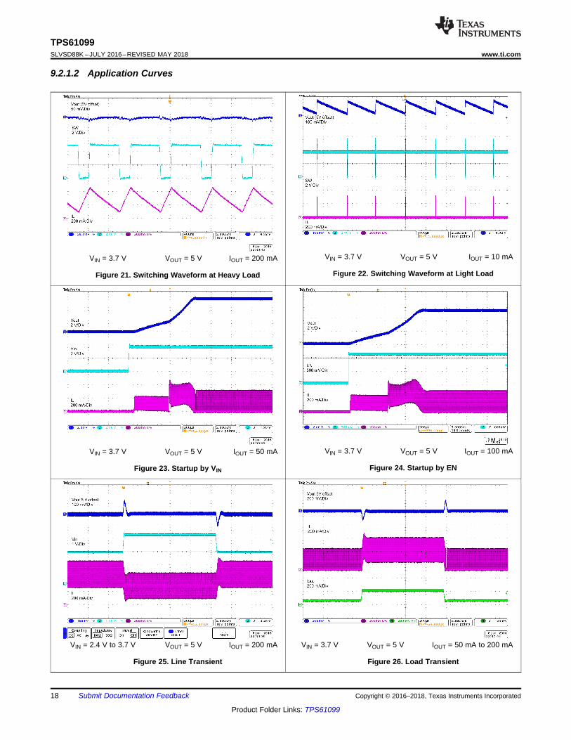
9.2.1.2 Application Curves
VIN = 3.7 V VOUT = 5 V IOUT = 200 mA
Figure 21. Switching Waveform at Heavy Load
VIN = 3.7 V VOUT = 5 V IOUT = 10 mA
Figure 22. Switching Waveform at Light Load
VIN = 3.7 V VOUT = 5 V IOUT = 50 mA
Figure 23. Startup by VIN
VIN = 3.7 V VOUT = 5 V IOUT = 100 mA
Figure 24. Startup by EN
VIN = 2.4 V to 3.7 V VOUT = 5 V IOUT = 200 mA
Figure 25. Line Transient
VIN = 3.7 V VOUT = 5 V IOUT = 50 mA to 200 mA
Figure 26. Load Transient
19
TPS61099www.ti.com SLVSD88K –JULY 2016–REVISED MAY 2018
Product Folder Links: TPS61099
Submit Documentation FeedbackCopyright © 2016–2018, Texas Instruments Incorporated
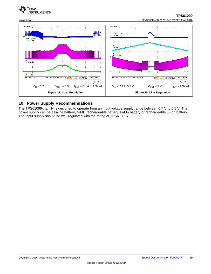
VIN = 3.7 V VOUT = 5 V IOUT = 0 mA to 250 mA
Figure 27. Load Regulation
VIN = 2.4 to 5.5 V VOUT = 5 V IOUT = 200 mA
Figure 28. Line Regulation
10 Power Supply RecommendationsThe TPS61099x family is designed to operate from an input voltage supply range between 0.7 V to 5.5 V. Thepower supply can be alkaline battery, NiMH rechargeable battery, Li-Mn battery or rechargeable Li-Ion battery.The input supply should be well regulated with the rating of TPS61099x.
VIN GND
SW VOUT
EN FB
INPUT GROUND
OUTPUT
ENGROUND
Top Layer
VIA
20
TPS61099SLVSD88K –JULY 2016–REVISED MAY 2018 www.ti.com
Product Folder Links: TPS61099
Submit Documentation Feedback Copyright © 2016–2018, Texas Instruments Incorporated
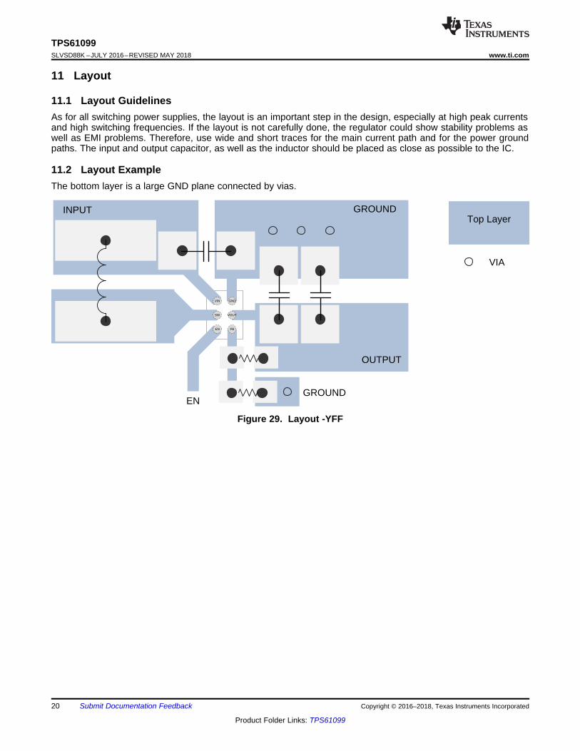
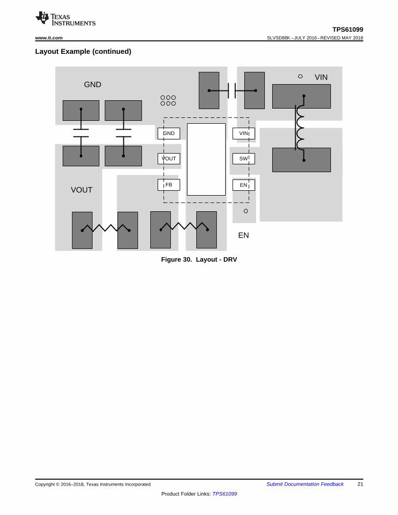
11 Layout
11.1 Layout GuidelinesAs for all switching power supplies, the layout is an important step in the design, especially at high peak currentsand high switching frequencies. If the layout is not carefully done, the regulator could show stability problems aswell as EMI problems. Therefore, use wide and short traces for the main current path and for the power groundpaths. The input and output capacitor, as well as the inductor should be placed as close as possible to the IC.
11.2 Layout ExampleThe bottom layer is a large GND plane connected by vias.
Figure 29. Layout -YFF
VOUT
FB
VIN
SW
EN
GND
GNDVIN
VOUT
EN
21
TPS61099www.ti.com SLVSD88K –JULY 2016–REVISED MAY 2018
Product Folder Links: TPS61099
Submit Documentation FeedbackCopyright © 2016–2018, Texas Instruments Incorporated
Layout Example (continued)
Figure 30. Layout - DRV
22
TPS61099SLVSD88K –JULY 2016–REVISED MAY 2018 www.ti.com
Product Folder Links: TPS61099
Submit Documentation Feedback Copyright © 2016–2018, Texas Instruments Incorporated
12 Device and Documentation Support
12.1 Device Support
12.1.1 Development Support
12.1.1.1 Custom Design With WEBENCH® ToolsClick here to create a custom design using the TPS61099x device with the WEBENCH® Power Designer.1. Start by entering the input voltage (VIN), output voltage (VOUT), and output current (IOUT) requirements.2. Optimize the design for key parameters such as efficiency, footprint, and cost using the optimizer dial.3. Compare the generated design with other possible solutions from Texas Instruments.
The WEBENCH Power Designer provides a customized schematic along with a list of materials with real-timepricing and component availability.
In most cases, these actions are available:• Run electrical simulations to see important waveforms and circuit performance• Run thermal simulations to understand board thermal performance• Export customized schematic and layout into popular CAD formats• Print PDF reports for the design, and share the design with colleagues
Get more information about WEBENCH tools at www.ti.com/WEBENCH.
12.1.2 Third-Party Products DisclaimerTI'S PUBLICATION OF INFORMATION REGARDING THIRD-PARTY PRODUCTS OR SERVICES DOES NOTCONSTITUTE AN ENDORSEMENT REGARDING THE SUITABILITY OF SUCH PRODUCTS OR SERVICESOR A WARRANTY, REPRESENTATION OR ENDORSEMENT OF SUCH PRODUCTS OR SERVICES, EITHERALONE OR IN COMBINATION WITH ANY TI PRODUCT OR SERVICE.
12.2 Documentation Support
12.2.1 Related DocumentationFor related documentation see the following:• Performing Accurate PFM Mode Efficiency Measurements, SLVA236• Accurately measuring efficiency of ultralow-IQ devices, SLYT558• IQ: What it is, what it isn’t, and how to use it, SLYT412
12.3 Receiving Notification of Documentation UpdatesTo receive notification of documentation updates, navigate to the device product folder on ti.com. In the upperright corner, click on Alert me to register and receive a weekly digest of any product information that haschanged. For change details, review the revision history included in any revised document.
12.4 Community ResourcesThe following links connect to TI community resources. Linked contents are provided "AS IS" by the respectivecontributors. They do not constitute TI specifications and do not necessarily reflect TI's views; see TI's Terms ofUse.
TI E2E™ Online Community TI's Engineer-to-Engineer (E2E) Community. Created to foster collaborationamong engineers. At e2e.ti.com, you can ask questions, share knowledge, explore ideas and helpsolve problems with fellow engineers.
Design Support TI's Design Support Quickly find helpful E2E forums along with design support tools andcontact information for technical support.
23
TPS61099www.ti.com SLVSD88K –JULY 2016–REVISED MAY 2018
Product Folder Links: TPS61099
Submit Documentation FeedbackCopyright © 2016–2018, Texas Instruments Incorporated
12.5 TrademarksE2E is a trademark of Texas Instruments.WEBENCH is a registered trademark of Texas Instruments.
12.6 Electrostatic Discharge CautionThese devices have limited built-in ESD protection. The leads should be shorted together or the device placed in conductive foamduring storage or handling to prevent electrostatic damage to the MOS gates.
12.7 GlossarySLYZ022 — TI Glossary.
This glossary lists and explains terms, acronyms, and definitions.
13 Mechanical, Packaging, and Orderable InformationThe following pages include mechanical packaging and orderable information. This information is the mostcurrent data available for the designated devices. This data is subject to change without notice and revision ofthis document. For browser-based versions of this data sheet, refer to the left-hand navigation.
PACKAGE OPTION ADDENDUM
www.ti.com 22-May-2018
Addendum-Page 1
PACKAGING INFORMATION
Orderable Device Status(1)
Package Type PackageDrawing
Pins PackageQty
Eco Plan(2)
Lead/Ball Finish(6)
MSL Peak Temp(3)
Op Temp (°C) Device Marking(4/5)
Samples
TPS610992YFFR ACTIVE DSBGA YFF 6 3000 Green (RoHS& no Sb/Br)
SNAGCU Level-1-260C-UNLIM -40 to 85 19J
TPS610992YFFT ACTIVE DSBGA YFF 6 250 Green (RoHS& no Sb/Br)
SNAGCU Level-1-260C-UNLIM -40 to 85 19J
TPS610993YFFR ACTIVE DSBGA YFF 6 3000 Green (RoHS& no Sb/Br)
SNAGCU Level-1-260C-UNLIM -40 to 85 17X
TPS610993YFFT ACTIVE DSBGA YFF 6 250 Green (RoHS& no Sb/Br)
SNAGCU Level-1-260C-UNLIM -40 to 85 17X
TPS610994YFFR ACTIVE DSBGA YFF 6 3000 Green (RoHS& no Sb/Br)
SNAGCU Level-1-260C-UNLIM -40 to 85 17N
TPS610994YFFT ACTIVE DSBGA YFF 6 250 Green (RoHS& no Sb/Br)
SNAGCU Level-1-260C-UNLIM -40 to 85 17N
TPS610995DRVR ACTIVE WSON DRV 6 3000 Green (RoHS& no Sb/Br)
CU NIPDAU Level-2-260C-1 YEAR -40 to 125 1NDU
TPS610995DRVT ACTIVE WSON DRV 6 250 Green (RoHS& no Sb/Br)
CU NIPDAU Level-2-260C-1 YEAR -40 to 125 1NDU
TPS610995YFFR ACTIVE DSBGA YFF 6 3000 Green (RoHS& no Sb/Br)
SNAGCU Level-1-260C-UNLIM -40 to 85 19K
TPS610995YFFT ACTIVE DSBGA YFF 6 250 Green (RoHS& no Sb/Br)
SNAGCU Level-1-260C-UNLIM -40 to 85 19K
TPS610996YFFR ACTIVE DSBGA YFF 6 3000 Green (RoHS& no Sb/Br)
SNAGCU Level-1-260C-UNLIM -40 to 85 19I
TPS610996YFFT ACTIVE DSBGA YFF 6 250 Green (RoHS& no Sb/Br)
SNAGCU Level-1-260C-UNLIM -40 to 85 19I
TPS610997YFFR ACTIVE DSBGA YFF 6 3000 Green (RoHS& no Sb/Br)
SNAGCU Level-1-260C-UNLIM -40 to 85 14K
TPS610997YFFT ACTIVE DSBGA YFF 6 250 Green (RoHS& no Sb/Br)
SNAGCU Level-1-260C-UNLIM -40 to 85 14K
TPS61099YFFR ACTIVE DSBGA YFF 6 3000 Green (RoHS& no Sb/Br)
SNAGCU Level-1-260C-UNLIM -40 to 85 12G
TPS61099YFFT ACTIVE DSBGA YFF 6 250 Green (RoHS& no Sb/Br)
SNAGCU Level-1-260C-UNLIM -40 to 85 12G
(1) The marketing status values are defined as follows:ACTIVE: Product device recommended for new designs.
PACKAGE OPTION ADDENDUM
www.ti.com 22-May-2018
Addendum-Page 2
LIFEBUY: TI has announced that the device will be discontinued, and a lifetime-buy period is in effect.NRND: Not recommended for new designs. Device is in production to support existing customers, but TI does not recommend using this part in a new design.PREVIEW: Device has been announced but is not in production. Samples may or may not be available.OBSOLETE: TI has discontinued the production of the device.
(2) RoHS: TI defines "RoHS" to mean semiconductor products that are compliant with the current EU RoHS requirements for all 10 RoHS substances, including the requirement that RoHS substancedo not exceed 0.1% by weight in homogeneous materials. Where designed to be soldered at high temperatures, "RoHS" products are suitable for use in specified lead-free processes. TI mayreference these types of products as "Pb-Free".RoHS Exempt: TI defines "RoHS Exempt" to mean products that contain lead but are compliant with EU RoHS pursuant to a specific EU RoHS exemption.Green: TI defines "Green" to mean the content of Chlorine (Cl) and Bromine (Br) based flame retardants meet JS709B low halogen requirements of <=1000ppm threshold. Antimony trioxide basedflame retardants must also meet the <=1000ppm threshold requirement.
(3) MSL, Peak Temp. - The Moisture Sensitivity Level rating according to the JEDEC industry standard classifications, and peak solder temperature.
(4) There may be additional marking, which relates to the logo, the lot trace code information, or the environmental category on the device.
(5) Multiple Device Markings will be inside parentheses. Only one Device Marking contained in parentheses and separated by a "~" will appear on a device. If a line is indented then it is a continuationof the previous line and the two combined represent the entire Device Marking for that device.
(6) Lead/Ball Finish - Orderable Devices may have multiple material finish options. Finish options are separated by a vertical ruled line. Lead/Ball Finish values may wrap to two lines if the finishvalue exceeds the maximum column width.
Important Information and Disclaimer:The information provided on this page represents TI's knowledge and belief as of the date that it is provided. TI bases its knowledge and belief on informationprovided by third parties, and makes no representation or warranty as to the accuracy of such information. Efforts are underway to better integrate information from third parties. TI has taken andcontinues to take reasonable steps to provide representative and accurate information but may not have conducted destructive testing or chemical analysis on incoming materials and chemicals.TI and TI suppliers consider certain information to be proprietary, and thus CAS numbers and other limited information may not be available for release.
In no event shall TI's liability arising out of such information exceed the total purchase price of the TI part(s) at issue in this document sold by TI to Customer on an annual basis.
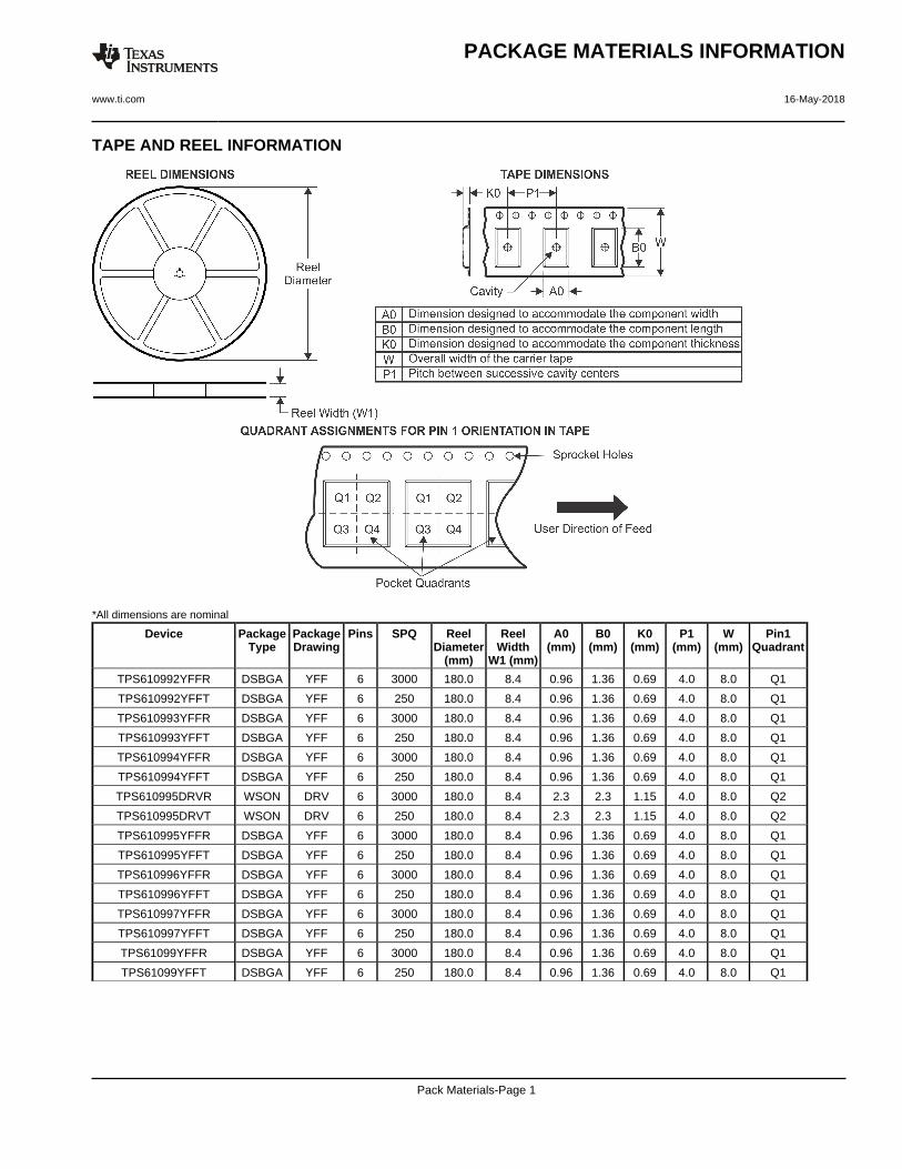
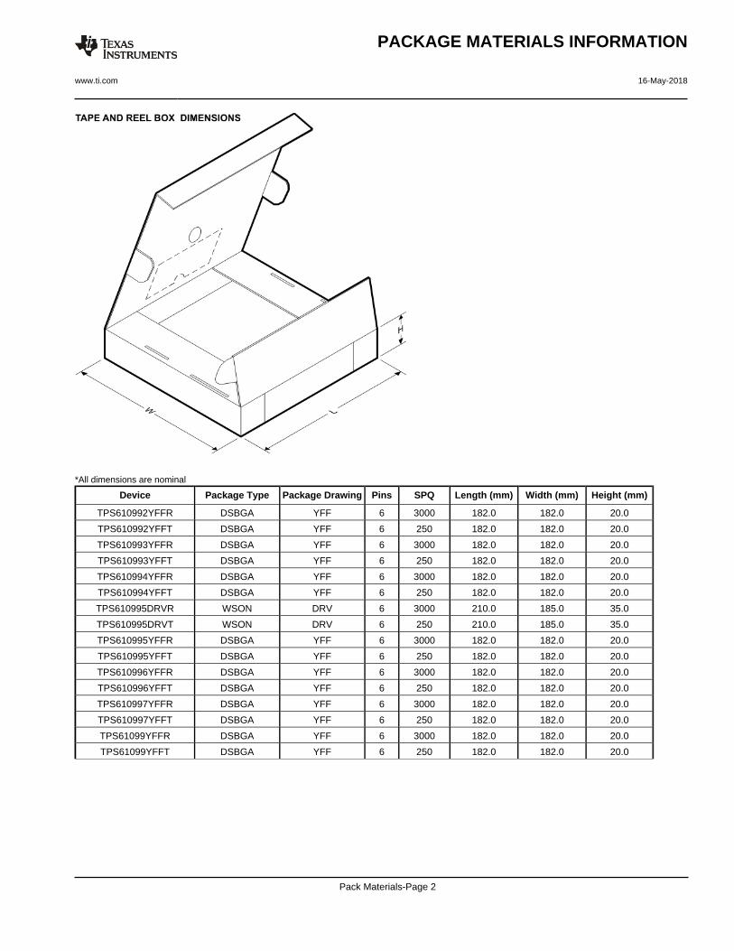
TAPE AND REEL INFORMATION
*All dimensions are nominal
Device PackageType
PackageDrawing
Pins SPQ ReelDiameter
(mm)
ReelWidth
W1 (mm)
A0(mm)
B0(mm)
K0(mm)
P1(mm)
W(mm)
Pin1Quadrant
TPS610992YFFR DSBGA YFF 6 3000 180.0 8.4 0.96 1.36 0.69 4.0 8.0 Q1
TPS610992YFFT DSBGA YFF 6 250 180.0 8.4 0.96 1.36 0.69 4.0 8.0 Q1
TPS610993YFFR DSBGA YFF 6 3000 180.0 8.4 0.96 1.36 0.69 4.0 8.0 Q1
TPS610993YFFT DSBGA YFF 6 250 180.0 8.4 0.96 1.36 0.69 4.0 8.0 Q1
TPS610994YFFR DSBGA YFF 6 3000 180.0 8.4 0.96 1.36 0.69 4.0 8.0 Q1
TPS610994YFFT DSBGA YFF 6 250 180.0 8.4 0.96 1.36 0.69 4.0 8.0 Q1
TPS610995DRVR WSON DRV 6 3000 180.0 8.4 2.3 2.3 1.15 4.0 8.0 Q2
TPS610995DRVT WSON DRV 6 250 180.0 8.4 2.3 2.3 1.15 4.0 8.0 Q2
TPS610995YFFR DSBGA YFF 6 3000 180.0 8.4 0.96 1.36 0.69 4.0 8.0 Q1
TPS610995YFFT DSBGA YFF 6 250 180.0 8.4 0.96 1.36 0.69 4.0 8.0 Q1
TPS610996YFFR DSBGA YFF 6 3000 180.0 8.4 0.96 1.36 0.69 4.0 8.0 Q1
TPS610996YFFT DSBGA YFF 6 250 180.0 8.4 0.96 1.36 0.69 4.0 8.0 Q1
TPS610997YFFR DSBGA YFF 6 3000 180.0 8.4 0.96 1.36 0.69 4.0 8.0 Q1
TPS610997YFFT DSBGA YFF 6 250 180.0 8.4 0.96 1.36 0.69 4.0 8.0 Q1
TPS61099YFFR DSBGA YFF 6 3000 180.0 8.4 0.96 1.36 0.69 4.0 8.0 Q1
TPS61099YFFT DSBGA YFF 6 250 180.0 8.4 0.96 1.36 0.69 4.0 8.0 Q1
PACKAGE MATERIALS INFORMATION
www.ti.com 16-May-2018
Pack Materials-Page 1
*All dimensions are nominal
Device Package Type Package Drawing Pins SPQ Length (mm) Width (mm) Height (mm)
TPS610992YFFR DSBGA YFF 6 3000 182.0 182.0 20.0
TPS610992YFFT DSBGA YFF 6 250 182.0 182.0 20.0
TPS610993YFFR DSBGA YFF 6 3000 182.0 182.0 20.0
TPS610993YFFT DSBGA YFF 6 250 182.0 182.0 20.0
TPS610994YFFR DSBGA YFF 6 3000 182.0 182.0 20.0
TPS610994YFFT DSBGA YFF 6 250 182.0 182.0 20.0
TPS610995DRVR WSON DRV 6 3000 210.0 185.0 35.0
TPS610995DRVT WSON DRV 6 250 210.0 185.0 35.0
TPS610995YFFR DSBGA YFF 6 3000 182.0 182.0 20.0
TPS610995YFFT DSBGA YFF 6 250 182.0 182.0 20.0
TPS610996YFFR DSBGA YFF 6 3000 182.0 182.0 20.0
TPS610996YFFT DSBGA YFF 6 250 182.0 182.0 20.0
TPS610997YFFR DSBGA YFF 6 3000 182.0 182.0 20.0
TPS610997YFFT DSBGA YFF 6 250 182.0 182.0 20.0
TPS61099YFFR DSBGA YFF 6 3000 182.0 182.0 20.0
TPS61099YFFT DSBGA YFF 6 250 182.0 182.0 20.0
PACKAGE MATERIALS INFORMATION
www.ti.com 16-May-2018
Pack Materials-Page 2
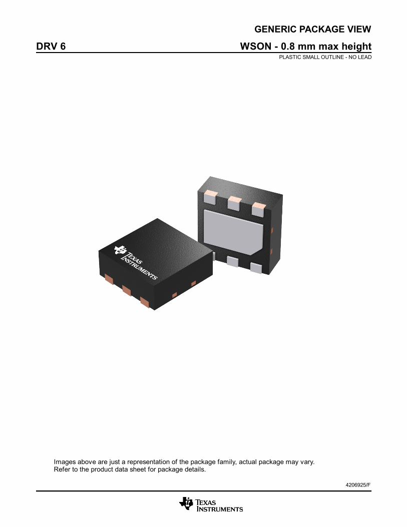
GENERIC PACKAGE VIEW
Images above are just a representation of the package family, actual package may vary.Refer to the product data sheet for package details.
DRV 6 WSON - 0.8 mm max heightPLASTIC SMALL OUTLINE - NO LEAD
4206925/F
www.ti.com
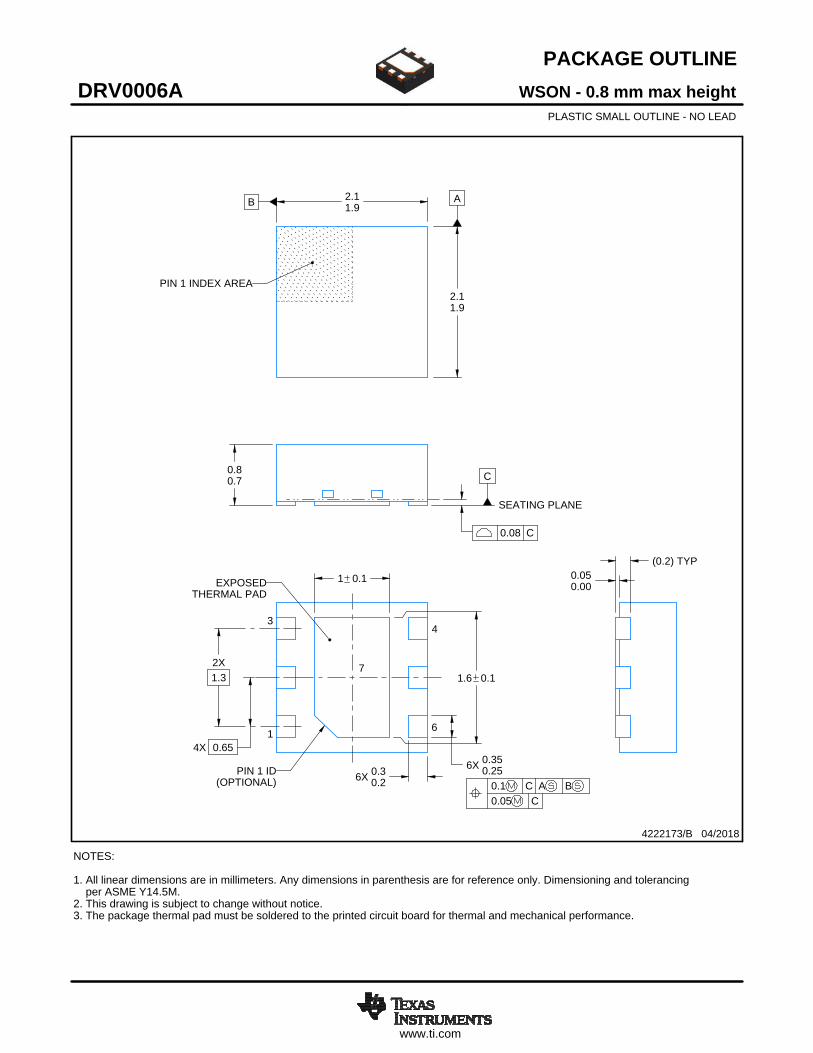
PACKAGE OUTLINE
C
6X 0.350.25
1.6 0.1
6X 0.30.2
2X1.3
1 0.1
4X 0.65
0.80.7
0.050.00
B 2.11.9
A
2.11.9
(0.2) TYP
WSON - 0.8 mm max heightDRV0006APLASTIC SMALL OUTLINE - NO LEAD
4222173/B 04/2018
PIN 1 INDEX AREA
SEATING PLANE
0.08 C
1
34
6
(OPTIONAL)PIN 1 ID
0.1 C A B0.05 C
THERMAL PADEXPOSED
7
NOTES: 1. All linear dimensions are in millimeters. Any dimensions in parenthesis are for reference only. Dimensioning and tolerancing per ASME Y14.5M. 2. This drawing is subject to change without notice. 3. The package thermal pad must be soldered to the printed circuit board for thermal and mechanical performance.
SCALE 5.500
www.ti.com
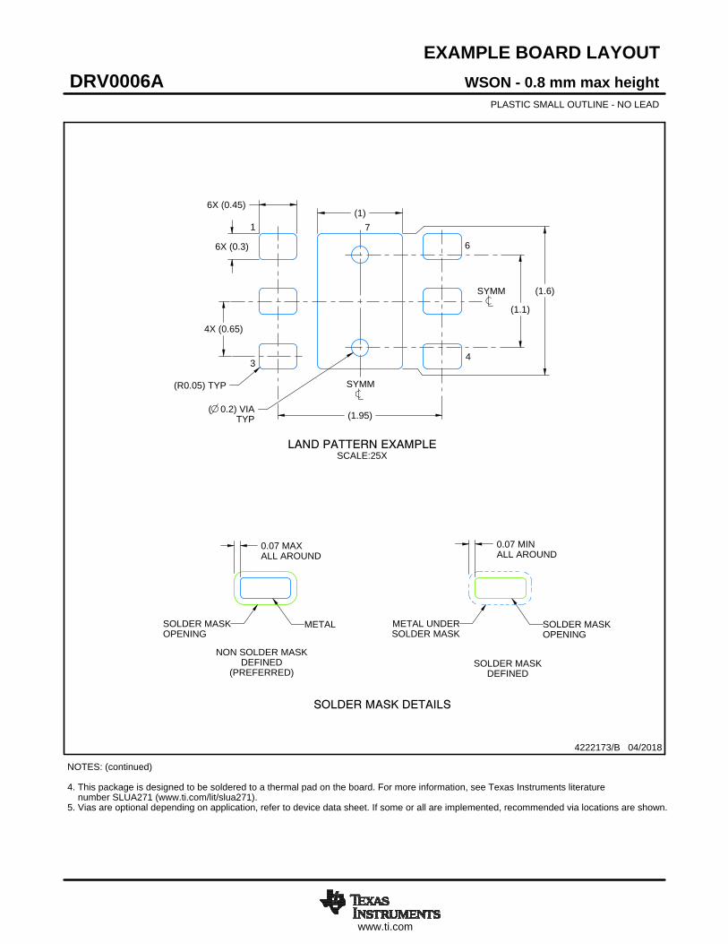
EXAMPLE BOARD LAYOUT
0.07 MINALL AROUND
0.07 MAXALL AROUND
(1)
4X (0.65)
(1.95)
6X (0.3)
6X (0.45)
(1.6)
(R0.05) TYP
( 0.2) VIATYP
(1.1)
WSON - 0.8 mm max heightDRV0006APLASTIC SMALL OUTLINE - NO LEAD
4222173/B 04/2018
SYMM
1
34
6
SYMM
LAND PATTERN EXAMPLESCALE:25X
7
NOTES: (continued) 4. This package is designed to be soldered to a thermal pad on the board. For more information, see Texas Instruments literature number SLUA271 (www.ti.com/lit/slua271).5. Vias are optional depending on application, refer to device data sheet. If some or all are implemented, recommended via locations are shown.
SOLDER MASKOPENINGSOLDER MASK
METAL UNDER
SOLDER MASKDEFINED
METALSOLDER MASKOPENING
SOLDER MASK DETAILS
NON SOLDER MASKDEFINED
(PREFERRED)
www.ti.com
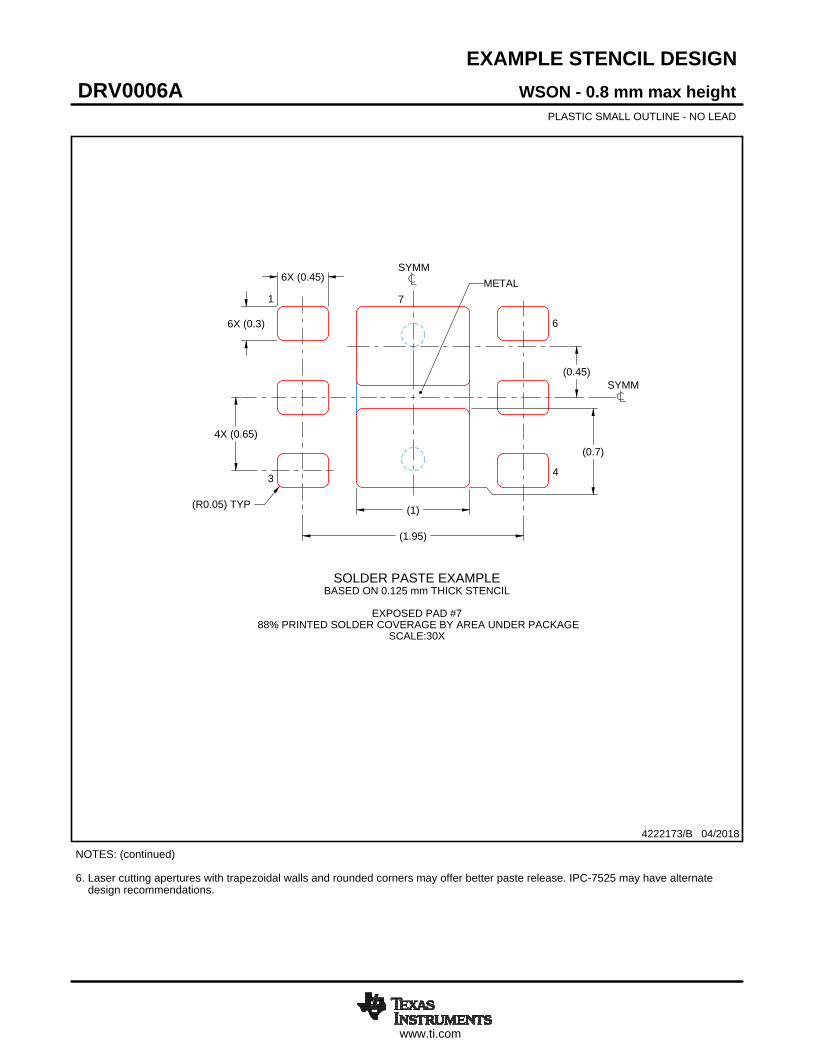
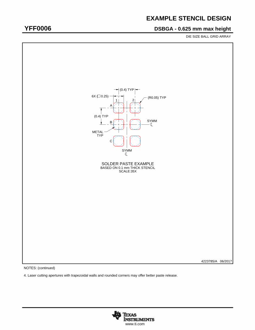
EXAMPLE STENCIL DESIGN
6X (0.3)
6X (0.45)
4X (0.65)
(0.7)
(1)
(1.95)
(R0.05) TYP
(0.45)
WSON - 0.8 mm max heightDRV0006APLASTIC SMALL OUTLINE - NO LEAD
4222173/B 04/2018
NOTES: (continued) 6. Laser cutting apertures with trapezoidal walls and rounded corners may offer better paste release. IPC-7525 may have alternate design recommendations.
SOLDER PASTE EXAMPLEBASED ON 0.125 mm THICK STENCIL
EXPOSED PAD #7
88% PRINTED SOLDER COVERAGE BY AREA UNDER PACKAGESCALE:30X
SYMM
1
3 4
6
SYMM
METAL7
www.ti.com
PACKAGE OUTLINE
C0.625 MAX
0.300.12
0.8TYP
0.4 TYP
0.4 TYP
6X 0.30.2
B E A
D
DSBGA - 0.625 mm max heightYFF0006DIE SIZE BALL GRID ARRAY
4223785/A 06/2017
NOTES: 1. All linear dimensions are in millimeters. Any dimensions in parenthesis are for reference only. Dimensioning and tolerancing per ASME Y14.5M.2. This drawing is subject to change without notice.
BALL A1CORNER
SEATING PLANE
BALL TYP 0.05 C
B
1 2
0.015 C A B
SYMM
SYMM
A
C
SCALE 10.500
D: Max =
E: Max =
1.256 mm, Min =
0.914 mm, Min =
1.196 mm
0.854 mm
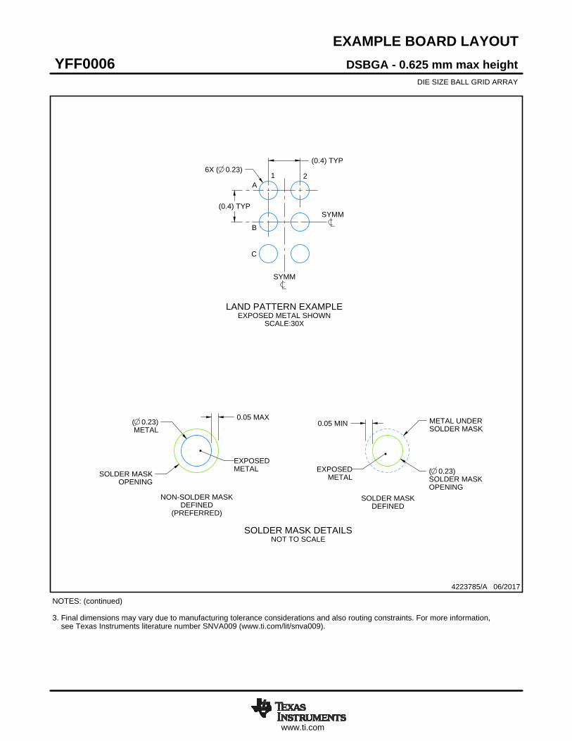
www.ti.com
EXAMPLE BOARD LAYOUT
6X ( 0.23)(0.4) TYP
(0.4) TYP
( 0.23)METAL
0.05 MAX
SOLDER MASKOPENING
METAL UNDERSOLDER MASK
( 0.23)SOLDER MASKOPENING
0.05 MIN
DSBGA - 0.625 mm max heightYFF0006DIE SIZE BALL GRID ARRAY
4223785/A 06/2017
NOTES: (continued) 3. Final dimensions may vary due to manufacturing tolerance considerations and also routing constraints. For more information, see Texas Instruments literature number SNVA009 (www.ti.com/lit/snva009).
SYMM
SYMM
LAND PATTERN EXAMPLEEXPOSED METAL SHOWN
SCALE:30X
C
1 2A
B
NON-SOLDER MASKDEFINED
(PREFERRED)
SOLDER MASK DETAILSNOT TO SCALE
EXPOSEDMETAL
SOLDER MASKDEFINED
EXPOSEDMETAL
www.ti.com
EXAMPLE STENCIL DESIGN
(0.4) TYP
(0.4) TYP
6X ( 0.25) (R0.05) TYP
METALTYP
DSBGA - 0.625 mm max heightYFF0006DIE SIZE BALL GRID ARRAY
4223785/A 06/2017
NOTES: (continued) 4. Laser cutting apertures with trapezoidal walls and rounded corners may offer better paste release.
SYMM
SYMM
C
1 2A
B
SOLDER PASTE EXAMPLEBASED ON 0.1 mm THICK STENCIL
SCALE:35X
IMPORTANT NOTICE
Texas Instruments Incorporated (TI) reserves the right to make corrections, enhancements, improvements and other changes to itssemiconductor products and services per JESD46, latest issue, and to discontinue any product or service per JESD48, latest issue. Buyersshould obtain the latest relevant information before placing orders and should verify that such information is current and complete.TI’s published terms of sale for semiconductor products (http://www.ti.com/sc/docs/stdterms.htm) apply to the sale of packaged integratedcircuit products that TI has qualified and released to market. Additional terms may apply to the use or sale of other types of TI products andservices.Reproduction of significant portions of TI information in TI data sheets is permissible only if reproduction is without alteration and isaccompanied by all associated warranties, conditions, limitations, and notices. TI is not responsible or liable for such reproduceddocumentation. Information of third parties may be subject to additional restrictions. Resale of TI products or services with statementsdifferent from or beyond the parameters stated by TI for that product or service voids all express and any implied warranties for theassociated TI product or service and is an unfair and deceptive business practice. TI is not responsible or liable for any such statements.Buyers and others who are developing systems that incorporate TI products (collectively, “Designers”) understand and agree that Designersremain responsible for using their independent analysis, evaluation and judgment in designing their applications and that Designers havefull and exclusive responsibility to assure the safety of Designers' applications and compliance of their applications (and of all TI productsused in or for Designers’ applications) with all applicable regulations, laws and other applicable requirements. Designer represents that, withrespect to their applications, Designer has all the necessary expertise to create and implement safeguards that (1) anticipate dangerousconsequences of failures, (2) monitor failures and their consequences, and (3) lessen the likelihood of failures that might cause harm andtake appropriate actions. Designer agrees that prior to using or distributing any applications that include TI products, Designer willthoroughly test such applications and the functionality of such TI products as used in such applications.TI’s provision of technical, application or other design advice, quality characterization, reliability data or other services or information,including, but not limited to, reference designs and materials relating to evaluation modules, (collectively, “TI Resources”) are intended toassist designers who are developing applications that incorporate TI products; by downloading, accessing or using TI Resources in anyway, Designer (individually or, if Designer is acting on behalf of a company, Designer’s company) agrees to use any particular TI Resourcesolely for this purpose and subject to the terms of this Notice.TI’s provision of TI Resources does not expand or otherwise alter TI’s applicable published warranties or warranty disclaimers for TIproducts, and no additional obligations or liabilities arise from TI providing such TI Resources. TI reserves the right to make corrections,enhancements, improvements and other changes to its TI Resources. TI has not conducted any testing other than that specificallydescribed in the published documentation for a particular TI Resource.Designer is authorized to use, copy and modify any individual TI Resource only in connection with the development of applications thatinclude the TI product(s) identified in such TI Resource. NO OTHER LICENSE, EXPRESS OR IMPLIED, BY ESTOPPEL OR OTHERWISETO ANY OTHER TI INTELLECTUAL PROPERTY RIGHT, AND NO LICENSE TO ANY TECHNOLOGY OR INTELLECTUAL PROPERTYRIGHT OF TI OR ANY THIRD PARTY IS GRANTED HEREIN, including but not limited to any patent right, copyright, mask work right, orother intellectual property right relating to any combination, machine, or process in which TI products or services are used. Informationregarding or referencing third-party products or services does not constitute a license to use such products or services, or a warranty orendorsement thereof. Use of TI Resources may require a license from a third party under the patents or other intellectual property of thethird party, or a license from TI under the patents or other intellectual property of TI.TI RESOURCES ARE PROVIDED “AS IS” AND WITH ALL FAULTS. TI DISCLAIMS ALL OTHER WARRANTIES ORREPRESENTATIONS, EXPRESS OR IMPLIED, REGARDING RESOURCES OR USE THEREOF, INCLUDING BUT NOT LIMITED TOACCURACY OR COMPLETENESS, TITLE, ANY EPIDEMIC FAILURE WARRANTY AND ANY IMPLIED WARRANTIES OFMERCHANTABILITY, FITNESS FOR A PARTICULAR PURPOSE, AND NON-INFRINGEMENT OF ANY THIRD PARTY INTELLECTUALPROPERTY RIGHTS. TI SHALL NOT BE LIABLE FOR AND SHALL NOT DEFEND OR INDEMNIFY DESIGNER AGAINST ANY CLAIM,INCLUDING BUT NOT LIMITED TO ANY INFRINGEMENT CLAIM THAT RELATES TO OR IS BASED ON ANY COMBINATION OFPRODUCTS EVEN IF DESCRIBED IN TI RESOURCES OR OTHERWISE. IN NO EVENT SHALL TI BE LIABLE FOR ANY ACTUAL,DIRECT, SPECIAL, COLLATERAL, INDIRECT, PUNITIVE, INCIDENTAL, CONSEQUENTIAL OR EXEMPLARY DAMAGES INCONNECTION WITH OR ARISING OUT OF TI RESOURCES OR USE THEREOF, AND REGARDLESS OF WHETHER TI HAS BEENADVISED OF THE POSSIBILITY OF SUCH DAMAGES.Unless TI has explicitly designated an individual product as meeting the requirements of a particular industry standard (e.g., ISO/TS 16949and ISO 26262), TI is not responsible for any failure to meet such industry standard requirements.Where TI specifically promotes products as facilitating functional safety or as compliant with industry functional safety standards, suchproducts are intended to help enable customers to design and create their own applications that meet applicable functional safety standardsand requirements. Using products in an application does not by itself establish any safety features in the application. Designers mustensure compliance with safety-related requirements and standards applicable to their applications. Designer may not use any TI products inlife-critical medical equipment unless authorized officers of the parties have executed a special contract specifically governing such use.Life-critical medical equipment is medical equipment where failure of such equipment would cause serious bodily injury or death (e.g., lifesupport, pacemakers, defibrillators, heart pumps, neurostimulators, and implantables). Such equipment includes, without limitation, allmedical devices identified by the U.S. Food and Drug Administration as Class III devices and equivalent classifications outside the U.S.TI may expressly designate certain products as completing a particular qualification (e.g., Q100, Military Grade, or Enhanced Product).Designers agree that it has the necessary expertise to select the product with the appropriate qualification designation for their applicationsand that proper product selection is at Designers’ own risk. Designers are solely responsible for compliance with all legal and regulatoryrequirements in connection with such selection.Designer will fully indemnify TI and its representatives against any damages, costs, losses, and/or liabilities arising out of Designer’s non-compliance with the terms and provisions of this Notice.
Mailing Address: Texas Instruments, Post Office Box 655303, Dallas, Texas 75265Copyright © 2018, Texas Instruments Incorporated