Embed Size (px)
Citation preview

GND
SW
BOOTVIN
RT/CLK
SS
RST
FB1
EN2
COMP
TPS65321-Q1
EN1
PowerPAD
LDO_OUTVIN_LDO
FB2
VI = 3.6 V to 36 V
1.1 V to 5.5 V,280 mA
1.1 V to 20 V,3.2 A
LDO Regulator
Control
VI = 3 V to 36 V
Buck Regulator
Control
Supply
Supply
Copyright © 2017, Texas Instruments Incorporated
Load Current (A)
Effi
cien
cy (
%)
0 1 2 3 40
10
20
30
40
50
60
70
80
90
100
D001
fs = 300 kHzfs = 2 MHz
Product
Folder
Order
Now
Technical
Documents
Tools &
Software
Support &Community
An IMPORTANT NOTICE at the end of this data sheet addresses availability, warranty, changes, use in safety-critical applications,intellectual property matters and other important disclaimers. PRODUCTION DATA.
TPS65321A-Q1SLVSE55 –NOVEMBER 2017
TPS65321A-Q1 36-V Step-Down Converter With Eco-mode™ and LDO Regulator
1
1 Features1• Qualified for Automotive Applications• AEC-Q100 Qualified with the Following Results:
– Device Temperature Grade 1: –40°C to+125°C Ambient Operating Temperature
– Device HBM ESD Classification Level 2– Device CDM ESD Classification Level C4B
• One High-VIN Step-Down DC-DC Converter– Input Range of 3.6 V to 36 V– 250-mΩ High-Side MOSFET– Maximum Load Current 3.2 A, Output
Adjustable 1.1 V to 20 V– Adjustable Switching Frequency 100 kHz to
2.5 MHz– Synchronizes to External Clock– High Efficiency at Light Loads With Pulse-
Skipping Eco-mode™ Control Scheme– Maximum 140-µA Operating Quiescent
Current– Reset Output-Pin (Active Low, Open-Drain)
• One High-VIN Low-Dropout (LDO) VoltageRegulator– Input Range of 3 V to 36 V– 280-mA Current Capability With Typical 35-µA
Quiescent Current in No-Load Condition– Low-Dropout Voltage of 300 mV at
IO = 200 mA (Typical)• Overcurrent Protection for Both Regulators• Overtemperature Protection• 14-Pin HTSSOP Package With PowerPAD™
Integrated Circuit Package
2 Applications• Automotive Infotainment and Cluster• Advanced Driver Assistance System (ADAS)• Automotive Telematics, eCall
3 DescriptionThe TPS65321A-Q1 device is a combination of ahigh-VIN DC-DC step-down converter, referred to asthe buck regulator, with an adjustable switch-modefrequency from 100-kHz to 2.5-MHz, and a high-VIN280-mA low-dropout (LDO) regulator. The input rangeis 3.6 V to 36 V for the buck regulator, and 3 V to36 V for the LDO regulator. The buck regulator hasan integrated high-side MOSFET with an active-low,open-drain power-good output-pin (nRST). The LDOregulator features a low-input supply current of 45-μAtypical in no-load, also has an integrated MOSFET.Low-voltage tracking feature enables TPS65321A-Q1to track the input supply during cold-crank conditions.
The buck regulator provides a flexible design to fitsystem needs. The external loop compensation circuitallows for optimization of the converter response forthe appropriate operating conditions. A low-ripplepulse-skip mode reduces the no-load input-supplycurrent to maximum 140 μA.
The device has built-in protection features such assoft start, current-limit, thermal sensing and shutdowndue to excessive power dissipation. Furthermore, thedevice has an internal undervoltage-lockout (UVLO)function that turns off the device when the supplyvoltage is too low.
Device Information(1)
PART NUMBER PACKAGE BODY SIZE (NOM)TPS65321A-Q1 HTSSOP (14) 5.00 mm × 4.40 mm
(1) For all available packages, see the orderable addendum atthe end of the data sheet.
Typical Application SchematicBuck Efficiency Versus Output Current

2
TPS65321A-Q1SLVSE55 –NOVEMBER 2017 www.ti.com
Product Folder Links: TPS65321A-Q1
Submit Documentation Feedback Copyright © 2017, Texas Instruments Incorporated
Table of Contents1 Features .................................................................. 12 Applications ........................................................... 13 Description ............................................................. 14 Revision History..................................................... 25 Pin Configuration and Functions ......................... 36 Specifications......................................................... 4
6.1 Absolute Maximum Ratings ..................................... 46.2 ESD Ratings.............................................................. 46.3 Recommended Operating Conditions....................... 56.4 Thermal Information .................................................. 56.5 Electrical Characteristics........................................... 66.6 Typical Characteristics .............................................. 8
7 Detailed Description ............................................ 107.1 Overview ................................................................. 107.2 Functional Block Diagram ....................................... 117.3 Feature Description................................................. 11
7.4 Device Functional Modes........................................ 218 Application and Implementation ........................ 22
8.1 Application Information............................................ 228.2 Typical Application .................................................. 22
9 Power Supply Recommendations ...................... 3310 Layout................................................................... 33
10.1 Layout Guidelines ................................................. 3310.2 Layout Example .................................................... 34
11 Device and Documentation Support ................. 3511.1 Documentation Support ........................................ 3511.2 Receiving Notification of Documentation Updates 3511.3 Community Resources.......................................... 3511.4 Trademarks ........................................................... 3511.5 Electrostatic Discharge Caution............................ 3511.6 Glossary ................................................................ 35
12 Mechanical, Packaging, and OrderableInformation ........................................................... 35
4 Revision HistoryNOTE: Page numbers for previous revisions may differ from page numbers in the current version.
DATE REVISION NOTESNovember 2017 * Initial release.

Thermal
Pad
1BOOT 14 SW
2VIN 13 GND
3VIN_LDO 12 COMP
4LDO_OUT 11 FB1
5FB2 10 SS
6nRST 9 RT/CLK
7EN2 8 EN1
3
TPS65321A-Q1www.ti.com SLVSE55 –NOVEMBER 2017
Product Folder Links: TPS65321A-Q1
Submit Documentation FeedbackCopyright © 2017, Texas Instruments Incorporated
5 Pin Configuration and Functions
PWP Package14-Pin HTSSOP With Thermal Pad
Top View
Pin FunctionsPIN
I/O DESCRIPTIONNAME NO.
BOOT 1 O A bootstrap capacitor is required between the BOOT and SW pins to supply the bias voltage for the integratedhigh-side MOSFET.
COMP 12 O The COMP pin is the error-amplifier output of the buck regulator, and the input to the output switch-currentcomparator of the buck regulator. Connect frequency-compensation components to the COMP pin.
EN1 8 I The EN1 pin is the enable and disable input for the buck regulator (high-voltage tolerant) and is internallypulled to ground. Pull this pin up externally to enable the buck regulator.
EN2 7 I The EN2 pin is the enable and disable input for the LDO regulator (high-voltage tolerant) and is internallypulled to ground. Pull this pin up externally to enable the LDO regulator.
FB1 11 I The FB1 pin is the feedback pin of the buck regulator. Connect an external resistive divider between the buckregulator output, the FB2 pin, and the GND pin to set the desired output voltage of the buck regulator.
FB2 5 I The FB2 pin is the feedback pin of the LDO regulator. Connect an external resistive divider between theLDO_OUT pin, the FB2 pin, and the GND pin to set the desired output voltage of the LDO regulator.
GND 13 — This pin is the ground pin.LDO_OUT 4 O This pin is the LDO regulator output.
nRST 6 O The nRST pin is the active low, open drain reset output of the buck regulator. Connect this pin with an externalbias voltage through an external resistor. This pin is asserted high after the buck regulator begins regulating.
RT/CLK 9 IConnect this pin to an external resistor to ground to program the switching frequency of the buck regulator. Analternative option is to feed an external clock to provide a reference for the switching frequency of the buckregulator.
SS 10 I Connect this pin to an external capacitor to ground which sets the soft-start time of the buck regulator.SW 14 I The SW pin is the source node of the internal high-side MOSFET of the buck regulator.VIN 2 — The VIN pin is the input supply pin for the internal biasing and high-side MOSFET of the buck regulator.VIN_LDO 3 — The VIN_LDO pin is the input supply pin for the LDO regulator.ExposedPowerPAD — Electrically connect the PowerPAD to ground and solder to the ground plane of the PCB for thermal
performance.

4
TPS65321A-Q1SLVSE55 –NOVEMBER 2017 www.ti.com
Product Folder Links: TPS65321A-Q1
Submit Documentation Feedback Copyright © 2017, Texas Instruments Incorporated
(1) Stresses beyond those listed under Absolute Maximum Ratings may cause permanent damage to the device. These are stress ratingsonly, and functional operation of the device at these or any other conditions beyond those indicated under Recommended OperatingConditions is not implied. Exposure to absolute-maximum-rated conditions for extended periods may affect device reliability.
6 Specifications
6.1 Absolute Maximum Ratings (1)
over operating free-air temperature (unless otherwise noted)MIN MAX UNIT
Supply inputsVIN –0.3 40
VVIN_LDO –0.3 40
ControlEN1, EN2 –0.3 40
VEN1-VIN, EN2-VIN 1
Buck converter
FB1 –0.3 3.6 V
SW –0.3–2 V for 30 ns 40 V
BOOT –0.3 46 VBOOT-SW 8 VCOMP –0.3 3.6 VSS –0.3 3.6 VRT/CLK, SS –0.3 3.6 VnRST –0.3 7 V
LDO regulatorLDO_OUT –0.3 7 VFB2 –0.3 7 V
Operating ambient temperature, TA -40 125 °COperating junction temperature, TJ –40 150 °CStorage temperature, Tstg –55 165 °C
(1) AEC Q100-002 indicates that HBM stressing shall be in accordance with the ANSI/ESDA/JEDEC JS-001 specification.
6.2 ESD RatingsVALUE UNIT
V(ESD)Electrostaticdischarge
Human-body model (HBM), per AEC Q100-002 (1) ±2000V
Charged-device model (CDM), per AEC Q100-011All pins ±500Corner pins (1, 7, 8, and 14) ±750

5
TPS65321A-Q1www.ti.com SLVSE55 –NOVEMBER 2017
Product Folder Links: TPS65321A-Q1
Submit Documentation FeedbackCopyright © 2017, Texas Instruments Incorporated
6.3 Recommended Operating Conditionsover operating free-air temperature range (unless otherwise noted)
MIN MAX UNIT
Supply inputsVIN 3.6 36
VVIN_LDO 3 36
Buck regulator
BOOT 3.6 42
V
SW1 –1 36FB1 0 0.8SS 0 3COMP 0 3RT/CLK 0 3nRST 0 5.25
LDO regulatorLDO_OUT 1.1 5.5
VFB2 0 0.8
ControlEN1 0 36
VEN2 0 36
Temperature Operating junction temperature range, TJ –40 150 °C
(1) For more information about traditional and new thermal metrics, see the Semiconductor and IC Package Thermal Metrics applicationreport.
6.4 Thermal Information
THERMAL METRIC (1)TPS65321A-Q1
UNITPWP (HTSSOP)14 PINS
RθJA Junction-to-ambient thermal resistance 41.0 °C/WRθJC(top) Junction-to-case (top) thermal resistance 33.1 °C/WRθJB Junction-to-board thermal resistance 25.4 °C/WψJT Junction-to-top characterization parameter 1.6 °C/WψJB Junction-to-board characterization parameter 25.1 °C/WRθJC(bot) Junction-to-case (bottom) thermal resistance 2.7 °C/W

6
TPS65321A-Q1SLVSE55 –NOVEMBER 2017 www.ti.com
Product Folder Links: TPS65321A-Q1
Submit Documentation Feedback Copyright © 2017, Texas Instruments Incorporated
6.5 Electrical CharacteristicsVI = 6 V to 27 V, EN1 = EN2 = VI, over-operating free-air temperature range TA = –40°C to 125°C and maximum operatingjunction temperature TJ = –150°C, unless otherwise noted. VI is the voltage on the battery-supply pins, VIN and VIN_LDO.
PARAMETER TEST CONDITIONS MIN TYP MAX UNITVIN (INPUT POWER SUPPLY)
Operating input voltage Normal mode, after initial start-up 3.6 12 36 VShutdown supply current V(EN1) = V(EN2) = 0 V, 25°C 2 7 μAInitial start-up voltage 6 36 V
ENABLE AND UVLO (EN1 AND EN2 PINS)Enable low level 0.7 VEnable high level 2.5 V
V(VIN)(f) Internal UVLO falling threshold Ramp V(VIN) down until output turns OFF 1.8 2.6 3 VV(VIN)(r) Internal UVLO rising threshold Ramp V(VIN) up until output turns ON 2.2 2.8 3.2 VBUCK REGULATOR
I(Qon) Operating: non-switching supply Measured at the VIN pinV(FB1) = 0.83 V, V(VIN) = 12 V, 25°C 110 140 μA
Output capacitanceESR = 0.001 Ω to 0.1 Ω, large outputcapacitance may be required for loadtransient
10 μF
V(ref1) Voltage reference for FB1 pinBuck regulator output: 1.1 V to 20 V.Buck regulator in Continuous ConductingMode without Pulse-Skipping
0.788 0.8 0.812 V
DC output voltage accuracy Includes voltage references, DC load andline regulation, process and temperature -2 2 %
DC(LDR) DC Load regulation, ΔVOUT / VOUT IOUT = 0 to IOUTmax 0.5 %
T(LDSR) Transient load step responseV(VIN) = 12V, IOUT = 200 mA to 3A, TR =TF = 1 µs, Buck Output Voltage = 5V, ƒS= 2 MHz
5 %
BUCK REGULATOR: HIGH-SIDE MOSFETr(DS(on) HSFET)
On-resistance V(VIN) = 12 V, V(SW) = 6 V 127 250 mΩ
tonmin Minimum on-time ƒS = 2.5 MHz 115 nsBUCK REGULATOR: CURRENT-LIMIT
Current-limit threshold V(VIN) = 12 V, TJ = 25°C 4 6 ABUCK REGULATOR: TIMING RESISTOR AND EXTERNAL CLOCK (RT/CLK PIN)
ƒS Switching-frequency range
Under RT mode 100 2500 kHzUnder fixed-frequency PWM mode, with200 kΩ connected between RT/CLK andGND pins
523 585 640 kHz
Under CLK mode 300 2200 kHzMinimum CLK input pulse width Measures at CLK input = 2.2 MHz 30 ns
RT/CLK High threshold 1.9 2.2 VRT/CLK Low threshold 0.5 0.7 V
RT/CLK Falling edge to SW rising edgedelay
Measured at 500 kHz with external clockconnected to RT/CLK pin 60 ns
PLL Lock-in time Measured at 500 kHz 100 μsBUCK REGULATOR: INTERNAL SOFT START TIMER
IDischarge(SS) Soft-start Pin Discharge CurrentV(SS) = 1 V, EN1=0, TA = 25°C 50 400 μAV(SS) = 1 V, EN1=0, TA = 125°C 33 400 μA
LDO REGULATOR
ΔVO(ΔVI) Line regulationV(VIN_LDO) = 6 V to 30 V,I(LDO_OUT) = 10 mA,V(LDO_OUT) = 3.3 V
20 mV
7
TPS65321A-Q1www.ti.com SLVSE55 –NOVEMBER 2017
Product Folder Links: TPS65321A-Q1
Submit Documentation FeedbackCopyright © 2017, Texas Instruments Incorporated
Electrical Characteristics (continued)VI = 6 V to 27 V, EN1 = EN2 = VI, over-operating free-air temperature range TA = –40°C to 125°C and maximum operatingjunction temperature TJ = –150°C, unless otherwise noted. VI is the voltage on the battery-supply pins, VIN and VIN_LDO.
PARAMETER TEST CONDITIONS MIN TYP MAX UNIT
ΔVO(ΔIL) Load regulationI(LDO_OUT) = 10 mA to 200 mA,V(VIN_LDO) = 12 V,V(LDO_OUT) = 3.3 V
35 mV
VDROPOUTDropout voltage(V(VIN_LDO) – V(LDO_OUT))
I(LDO_OUT) = 200 mA 300 450 mV
I(LDO_OUT) Output current V(LDO_OUT) in regulation, V(VIN) ≥ 4V 280 mA
VI(VIN_LDO)Operating input voltage onVIN_LDO pin V(LDO_OUT) in regulation 3 36 V
V(ref2) Voltage reference at FB2 pin V(LDO_OUT) = 1.1 V to 5.5 V 0.788 0.8 0.812 V
ICL(LDO_OUT) Output current-limit V(LDO_OUT) = 0 V (the LDO_OUT pin isshorted to ground) 280 1000 mA
IQ(LDO) Quiescent current
V(VIN) = 12 VMeasured at VIN pinV(EN1) = 0 V, V(EN2) = 5 V, I(LDO_OUT) =0.01 mA to 0.75 mA
35 50 μA
PSRR Power supply ripple rejection
V(VIN_LDO)(rip) = 0.5 VPP,I(LDO_OUT) = 200 mA,frequency (ƒ) = 100 Hz,V(LDO_OUT) = 5 V and V(LDO_OUT) = 3.3 V
60 dB
V(VIN_LDO)(rip) = 0.5 VPP, I(LDO_OUT) = 200mA, ƒ = 150 kHz,V(LDO_OUT) = 5 V and V(LDO_OUT) = 3.3 V
30 dB
C(LDO_OUT) Output capacitor
ESR = 0.001 Ω to 100 mΩ, large outputcapacitance may be required for loadtransientV(LDO_OUT) ≥ 3.3 V
1 40 μF
C(LDO_OUT) Output capacitor
ESR = 0.001 Ω to 100 mΩ, large outputcapacitance may be required for loadtransient1.2 V ≤ V(LDO_OUT) < 3.3 V
20 40 μF
BUCK REGULATOR: RESET (nRST Pin)RESET threshold V(FB1) decreasing 85% 90% 95%
VOL Output lownRST pin asserted low due to fallingV(FB1), < 1-mA sinking current into nRSTpin
0 0.045 0.4 V
Filter time Delay before asserting nRST low 7 14 21 μsOVER TEMPERATURE PROTECTIONTSD Thermal-shutdown trip point 175 ºCThys Hysteresis 10 ºC

LDO Load Current (A)
Out
put V
olta
ge (
V)
0 0.05 0.1 0.15 0.2 0.25 0.3 0.35 0.43.282
3.284
3.286
3.288
3.29
3.292
3.294
3.296
3.298
3.3
3.302
C008LDO Load Current (mA)
Dro
pout
Vol
tage
(m
V)
0 50 100 150 200 250 300 350 4000
50
100
150
200
250
300
350
400
450
500
C009
Junction Temperature (°C)
Buc
k-R
egul
ator
Fee
dbac
k-V
olta
ge R
efer
ence
(V
)
-50 -25 0 25 50 75 100 125 1500.794
0.796
0.798
0.8
0.802
C007
0
500
1000
1500
2000
2500
3000
0 200 400 600 800 1000 1200 1400 1600
Sw
itchi
n F
requ
ency
(kH
z)
RT/CLK Resistance (k C003
0
10
20
30
40
50
60
70
80
90
100
0.0 0.1 0.2 0.3 0.4 0.5 0.6 0.7 0.8
RI1RPLQDO¦
SW
VFB1 (V) C004 Input Voltage (V)
Out
put V
olta
ge (
V)
3.6 4 4.4 4.8 5.2 5.6 61.5
2
2.5
3
3.5
4
4.5
5
5.5
6
C002
No Load100-mA Load1-A Load
8
TPS65321A-Q1SLVSE55 –NOVEMBER 2017 www.ti.com
Product Folder Links: TPS65321A-Q1
Submit Documentation Feedback Copyright © 2017, Texas Instruments Incorporated
6.6 Typical Characteristics
ƒS = 2 MHz 3.6 V ≤ V(VIN) ≤ 6 V
Figure 1. Maximum-Possible Buck-Regulator Output Voltage
V(VIN) = 12 V
Figure 2. Buck-Regulator Switching Frequency vs V(FB1)Feedback Voltage
V(VIN) = 12 V TJ = 25°C
Figure 3. Buck-Regulator Switching Frequency vs RT_CLKResistance
No Load V(VIN) = 12 V
Figure 4. Buck-Regulator Feedback-Voltage Reference(V(FB1)) vs Junction Temperature
V(VIN_LDO) = 5 V V(LDO_OUT) = 3.3 V
Figure 5. LDO-Regulator Load Regulation
V(LDO_OUT) = 5 V
Figure 6. LDO-Regulator Dropout Voltage vs Load Current

Junction Temperature (°C)
LDO
-Reg
ulat
or F
eedb
ack-
Vol
tage
Ref
eren
ce (
V)
-50 -25 0 25 50 75 100 125 1500.796
0.7965
0.797
0.7975
0.798
0.7985
0.799
0.7995
C010
9
TPS65321A-Q1www.ti.com SLVSE55 –NOVEMBER 2017
Product Folder Links: TPS65321A-Q1
Submit Documentation FeedbackCopyright © 2017, Texas Instruments Incorporated
Typical Characteristics (continued)
I(LDO_OUT) = 100 mA V(VIN_LDO) = 12 V
Figure 7. LDO-Regulator Feedback-Voltage Reference (V(FB2)) vs Junction Temperature

10
TPS65321A-Q1SLVSE55 –NOVEMBER 2017 www.ti.com
Product Folder Links: TPS65321A-Q1
Submit Documentation Feedback Copyright © 2017, Texas Instruments Incorporated
7 Detailed Description
7.1 OverviewThe TPS65321A-Q1 device is a 36-V, 3.2-A, DC-DC step-down converter (also referred to as a buck regulator)with a 280-mA low-dropout (LDO) linear regulator. Both of these regulators have low quiescent consumptionduring a light load to prolong battery life.
The buck regulator improves performance during line and load transients by implementing a constant-frequencyand current-mode control (CCM) that reduces output capacitance which simplifies external frequency-compensation design. The wide switching frequency of 100 kHz to 2500 kHz allows for efficiency and sizeoptimization when selecting the output-filter components. The switching frequency is adjusted by using a resistorto ground on the RT/CLK pin. The buck regulator has an internal phase-locked loop (PLL) on the RT/CLK pinthat synchronizes the power-switch turnon to the falling edge of an external system clock.
The TPS65321A-Q1 device reduces the external component count by integrating the boot recharge diode. Acapacitor between the BOOT pin and the SW pin supplies the bias voltage for the integrated high-side MOSFET.The TPS65321A-Q1 device can operate at high duty cycles under the dropout mode operation. The outputvoltage can step-down to as low as the 0.8-V reference. The soft start minimizes inrush currents and providespower-supply sequencing during power up. Connect a small-value capacitor to the pin to adjust the soft-starttime. For critical power-supply sequencing requirements couple a resistor divider to the pin.
The LDO regulator consumes only about a 35-µA current in light load. The LDO regulator also tracks the batterywhen the battery voltage is low (in a cold-crank condition).
The buck regulator of the TPS65321A-Q1 device has a power-good open-drain output (nRST) that asserts lowwhen the regulated output voltage is less than 90% (typical) of the nominal output voltage.

Error Amplifier
VoltageReference
FB1
SS/TR
COMP
RT/CLK
SW
BOOT
VIN
GND
EN1
Shutdown
EnableThreshold
Shutdown PWRGD
PowerPAD
SS
EN2
RST
LDO_OUT
FB2VIN_LDO
Thermal Shutdown
UVLO
ShutdownLogic
LogicUV
OV
+
+
Maximum Clamp
Overload Recovery
PWM Comparator
Logic
SlopeCompensation
FrequencyShift
MinimumClamp
Pulse Skip
Oscillator with PLL
VoltageSupervisor
0.8 V
Linear Regulator Control
OVTO
R Q
S
Boot UVLO
Boot Charge
CurrentSense
PWM Latch
+±
Copyright © 2017, Texas Instruments Incorporated
Shutdown
FB1
11
TPS65321A-Q1www.ti.com SLVSE55 –NOVEMBER 2017
Product Folder Links: TPS65321A-Q1
Submit Documentation FeedbackCopyright © 2017, Texas Instruments Incorporated
7.2 Functional Block Diagram
7.3 Feature Description
7.3.1 Buck Regulator
7.3.1.1 Fixed-Frequency PWM ControlThe TPS65321A-Q1 buck regulator uses an adjustable, fixed-frequency peak current-mode control. An internalvoltage reference compares the output voltage through external resistors on the FB1 pin to an error amplifierwhich drives the COMP pin. An internal oscillator initiates the turnon of the high-side power switch. The devicecompares the error amplifier output to the high-side power-switch current. When the power-switch currentreaches the level set by the COMP voltage, the power switch turns off. The COMP pin voltage increases anddecreases as the output current increases and decreases. The device implements a current-limit by clamping theCOMP pin voltage to a maximum level.
7.3.1.2 Slope Compensation OutputThe TPS65321A-Q1 buck regulator adds a compensating ramp to the switch-current signal. This slopecompensation prevents sub-harmonic oscillations. The available peak-inductor current remains constant over thefull duty-cycle range.

12
TPS65321A-Q1SLVSE55 –NOVEMBER 2017 www.ti.com
Product Folder Links: TPS65321A-Q1
Submit Documentation Feedback Copyright © 2017, Texas Instruments Incorporated
Feature Description (continued)7.3.1.3 Pulse-Skip Eco-mode™ Control SchemeThe TPS65321A-Q1 buck regulator operates in a pulse-skip mode at light load currents to improve efficiency byreducing switching and gate-drive losses. The design of the TPS65321A-Q1 buck regulator is such that if theoutput voltage is within regulation and the peak switch current at the end of any switching cycle is below thepulse-skipping-current threshold, the buck regulator enters pulse-skip mode. This current threshold is the currentlevel corresponding to a nominal COMP voltage, or 720 mV. The current at which entry to the pulse-skip modeoccurs depends on switching frequency, inductor selection, output-capacitor selection, and compensationnetwork.
In pulse-skip mode, the buck regulator clamps the COMP pin voltage at 720 mV, inhibiting the high-sideMOSFET. Further decreases in load current or in output voltage cannot drive the COMP pin below this clamp-voltage level. Because the buck regulator is not switching, the output voltage begins to decay. As the voltage-control loop compensates for the falling output voltage, the COMP pin voltage begins to rise. At this time, thehigh-side MOSFET turns on and a switching pulse initiates on the next switching cycle. The peak current is setby the COMP pin voltage. The output current recharges the output capacitor to the nominal voltage, then thepeak switch current begins to decrease, and eventually falls below the pulse-skip-mode threshold, at which timethe buck regulator enters Eco-mode again.
For pulse-skip-mode operation, the TPS65321A-Q1 buck regulator senses the peak current, not the average orload current. Therefore, the load current where the buck regulator enters pulse-skip mode is dependent on theoutput inductor value. When the load current is low and the output voltage is within regulation, the buck regulatorenters a sleep mode and draws only 140-µA input quiescent current. The internal PLL remains operating whenthe buck regulator is in sleep mode.
7.3.1.4 Dropout Mode Operation and Bootstrap Voltage (BOOT)The TPS65321A-Q1 buck regulator has an integrated boot regulator and requires a small ceramic capacitorbetween the BOOT pin and the SW pin to provide the gate-drive voltage for the high-side MOSFET. The BOOTcapacitor recharges when the high-side MOSFET is off and the low-side diode conducts. The value of thisceramic capacitor must be 0.1 μF. TI recommends a ceramic capacitor with an X7R or X5R grade dielectric anda voltage rating of 10 V or higher because of the stable characteristics over temperature and over voltage.
To improve drop out, the high-side MOSFET of the TPS65321A-Q1 buck regulator remains on for 7 consecutiveswitching cycles, and is forced off during the 8th switching cycle to allow the low-side diode to conduct andrefresh the charge on the BOOT capacitor. Because the current supplied by the BOOT capacitor is low, the high-side MOSFET can remain on before it is required to refresh the BOOT capacitor. The effective duty cycle of theswitching regulator under this operation can be higher than the fixed-frequency PWM operation through skippingswitching cycles.
7.3.1.5 Error AmplifierThe buck converter of the TPS65321A-Q1 buck regulator has a transconductance amplifier acting as the erroramplifier. The error amplifier compares the FB1 voltage to the lower of the internal soft-start (SS) voltage or theinternal 0.8-V voltage reference. The transconductance (gm) of the error amplifier is 310 µS during normaloperation. During the soft-start operation, the transconductance is a fraction of the normal operating gm. Whenthe voltage of the voltage on the FB1 pin is below 0.8 V and the buck regulator is regulating using an internal SSvoltage, the gm is 70 µS. For frequency compensation, external compensation components (capacitor with seriesresistor and an optional parallel capacitor) must be connected between the COMP pin and the GND pin.
7.3.1.6 Voltage ReferenceThe voltage reference system produces a precise ±2% voltage reference over temperature by scaling the outputof a temperature stable band-gap circuit.
7.3.1.7 Adjusting the Output VoltageA resistor divider from the output node to the FB1 pin sets the output voltage. TI recommends using 1%tolerance or better divider resistors. Start with 10 kΩ for the R2 resistor and use Equation 1 to calculate R1. Toimprove efficiency at light loads, consider using larger-value resistors. If the values are too high, the regulator ismore susceptible to noise, and voltage errors from the FB1 input current are noticeable.

Soft-Start Capacitance (nF)
Dis
char
ge T
ime
(µs)
0 2 4 6 8 10 120
100
200
300
400
500
600
D007
ss ssss
ref
t (ms) I (µA)C (nF)
V (V) 0.8
´
=
´
OV 0.8 (V)R1 R2
0.8 (V)
-
= ´
13
TPS65321A-Q1www.ti.com SLVSE55 –NOVEMBER 2017
Product Folder Links: TPS65321A-Q1
Submit Documentation FeedbackCopyright © 2017, Texas Instruments Incorporated
Feature Description (continued)
where• VO = buck regulator output voltage (1)
7.3.1.8 Soft-Start Pin (SS)The TPS65321A-Q1 buck regulator regulates the output voltage by referencing the lower of either the internalvoltage reference or the SS pin voltage. A capacitor on the SS pin to ground implements a soft-start time. TheTPS65321A-Q1 buck regulator has an internal pullup current source of 2 μA that charges the external soft-startcapacitor. Equation 2 shows the calculations for the soft-start time (10% to 90%). The voltage reference (Vref) is0.8 V and the soft-start current (Iss) is 2 μA. The soft-start capacitor must remain lower than 10 nF and greaterthan 1 nF.
where• The voltage reference (Vref) is 0.8 V.• The soft-start current (ISS) is 2 µA. (2)
To secure a smooth power up with effective soft-start, the delay between a shutdown event and a consecutivepower-up event (such as recovering from a UVLO event or from a thermal shutdown event) must be long enoughto allow a complete discharge of the soft-start capacitor. The soft-start capacitor is discharged through an internalFET when the buck is disabled (EN1 = low). Because the FET has a finite resistance, a minimum disable time isrequired to allow discharge of the capacitor. In either case, the buck must be disabled for at least 100 μs. Forsoft-start capacitance with values higher than 1.5 nF, the discharge time of the capacitor increases linearly asshown in Figure 8.
Figure 8. Soft-Start Capacitance Value versus Discharge Time
7.3.1.9 Reset Output, nRSTThe nRST pin pf the TPS65321A-Q1 is a open-drain output between the nRST pin and the GND pin. The power-on-reset output asserts low until the output voltage on the FB1 pin exceeds the setting thresholds (91%) and thedeglitch timer has expired. Additionally, whenever the EN1 pin is low or open, nRST immediately asserts lowregardless of the output voltage. If a thermal shutdown occurs because of excessive thermal conditions, this pinalso asserts low. When the nRST is released (not asserted low) an external resistor connected to any externalbias voltage pulls up this nRST pin.

L dc O dS
on I L hs d
(I R V V )1ƒ (max skip)
t (V I R V )
æ ö æ ö´ + += ´ç ÷ ç ÷
- ´ +è ø è ø
T 1.0888S
206033R (k )
ƒ (kHz)W =
14
TPS65321A-Q1SLVSE55 –NOVEMBER 2017 www.ti.com
Product Folder Links: TPS65321A-Q1
Submit Documentation Feedback Copyright © 2017, Texas Instruments Incorporated
Feature Description (continued)7.3.1.10 Overload-Recovery CircuitThe TPS65321A-Q1 buck regulator has an overload recovery (OLR) circuit. The OLR circuit soft-starts the outputfrom the overload voltage to the nominal regulation voltage on removal of the fault condition. The OLR circuitdischarges the SS pin to a voltage slightly greater than the FB1 pin voltage using an internal pulldown of 382 μAwhen the error amplifier changes to a high voltage from a fault condition. On removal of the fault condition, theoutput soft starts from the fault voltage to nominal output voltage.
7.3.1.11 Constant Switching Frequency and Timing Resistor (RT/CLK Pin)The switching frequency of the TPS65321A-Q1 buck regulator is adjustable over a wide range fromapproximately 100 kHz to 2500 kHz by placing a resistor on the RT/CLK pin. The RT/CLK pin voltage is 0.5 V(typical) and must have a resistor to ground to set the switching frequency. To determine the timing resistancefor a given switching frequency, use Equation 3 or the curves in Figure 2. To reduce the solution size, the usertypically sets the switching frequency as high as possible. However, consider tradeoffs of the supply efficiency,maximum input voltage, and minimum controllable on-time. The minimum controllable on-time is 100 ns (typical)and limits the maximum operating input voltage. The frequency-shift circuit also limits the maximum switchingfrequency. The following sections discuss more details of the maximum switching frequency.
(3)
7.3.1.12 Overcurrent Protection and Frequency ShiftThe TPS65321A-Q1 buck regulator implements current-mode control, which uses the COMP pin voltage to turnoff the high-side MOSFET on a cycle-by-cycle basis. During each cycle, the switch current and COMP pinvoltage are compared. When the peak-switch current intersects the COMP voltage, the high-side switch turns off.During overcurrent conditions that pull the output voltage low, the error amplifier responds by driving the COMPpin high, increasing the switch current. Internal clamping of the error-amplifier output functions as a switchcurrent-limit.
The TPS65321A-Q1 buck regulator also implements a frequency shift. The switching frequency is divided by 8,4, 2, and 1 as the voltage ramps from 0 to 0.8 V on the FB1 pin. During short-circuit events (particularly withhigh-input-voltage applications), the control loop has a finite minimum controllable on-time, and the output has alow voltage. During the switch on-time, the inductor current ramps to the peak current-limit because of the highinput voltage and minimum on-time. During the switch off-time, the inductor typically does not have enough off-time and output voltage for the inductor to ramp down by the ramp-up amount. The frequency shift effectivelyincreases the off-time which allows the current to ramp down.
7.3.1.13 Selecting the Switching FrequencyThe switching frequency that is selected must be the lower value of the two equations, Equation 4 andEquation 5. Equation 4 is the maximum switching-frequency limitation set by the minimum controllable on-time.Setting the switching frequency above this value causes the regulator to skip switching pulses. The devicemaintains regulation, but pulse-skipping leads to high inductor current and a significant increase in output ripplevoltage.
Use Equation 5 to calculate the maximum switching frequency limit set by the frequency-shift protection. Foradequate output short-circuit protection at high input voltages, set the switching frequency to a value less thanthe ƒS(maxshift) frequency. In Equation 5, to calculate the maximum switching frequency one must take intoaccount that the output voltage decreases from the nominal voltage to 0 volts, and the ƒdiv integer increases from1 to 8 corresponding to the frequency shift.
where• IL = inductor current• Rdc = inductor resistance• VI = maximum input voltage

0
500
1000
1500
2000
2500
10 20 30 40 50 60
Sw
itchi
n F
requ
ency
(kH
z)
Input Voltage (V)
fsw (Max Skip)
fsw (Shift)
C012
¦S (max skip)
¦S (shift)
L dc O(SC) ddivS
on I L hs d
(I R V V )ƒƒ (shift)
t (V I R V )
´ + +æ öæ ö= ´ ç ÷ç ÷ ç ÷- ´ +è ø è ø
15
TPS65321A-Q1www.ti.com SLVSE55 –NOVEMBER 2017
Product Folder Links: TPS65321A-Q1
Submit Documentation FeedbackCopyright © 2017, Texas Instruments Incorporated
Feature Description (continued)• VO = buck regulator output voltage• Vd = diode voltage drop• Rhs = FET on resistance (127 mΩ, trypical)• ton = controllable on-time (100 ns, typical) (4)
where• VO(SC) = buck regulator output voltage during short-circuit condition• ƒdiv = frequency divide factor (equals 1, 2, 4 or 8) (5)
In Figure 9 the solid line illustrates a typical safe operating area regarding frequency shift and assumes theoutput voltage is 0 V, the resistance of the inductor is 0.13 Ω, the FET on-resistance is 0.127 Ω, and the diodevoltage drop is 0.5 V. The dashed line is the maximum switching frequency to avoid pulse skipping.
VO = 3.3 V IL = 1 A
Figure 9. Maximum Switching Frequency Versus Input Voltage
7.3.1.14 How to Interface to RT/CLK PinThe RT/CLK pin synchronizes the buck regulator to an external system clock. To implement the synchronizationfeature, connect a square wave to the RT/CLK pin through the circuit network shown in Figure 10. The square-wave amplitude must transition lower than 0.5 V and higher than 2.2 V on the RT/CLK pin and must have an on-time greater than 40 ns and an off-time greater than 40 ns. The synchronization frequency range is 300 kHz to2200 kHz. The rising edge of the SW pin synchronizes with the falling edge of the RT/CLK pin signal. Design theexternal synchronization circuit in such a way that the device has the default frequency-set resistor connectedfrom the RT/CLK pin to ground if the synchronization signal turns off. TI recommends using a frequency-setresistor connected as shown in Figure 10 through a 50-Ω resistor to ground. The resistor must set the switchingfrequency close to the external CLK frequency. TI also recommends AC-coupling the synchronization signalthrough a 10-pF ceramic capacitor to the RT/CLK pin and a 4-kΩ series resistor. The series resistor reduces SWjitter in heavy-load applications when synchronizing to an external clock, and in applications that transition fromsynchronizing to RT mode. The first time CLK is pulled above the CLK threshold, the device switches from theRT resistor frequency to PLL mode. Along with the resulting removal of the internal 0.5-V voltage source, theCLK pin becomes high-impedance as the PLL starts to lock onto the external signal. Because there is a PLL onthe buck regulator, the switching frequency can be higher or lower than the frequency set with the externalresistor. The buck regulator transitions from the resistor mode to the PLL mode and then increases or decreasesthe switching frequency until the PLL locks onto the CLK frequency within 100 ms.

PLLRT/CLK
External Clock
Source
Rfset
4 k
50
10 F
16
TPS65321A-Q1SLVSE55 –NOVEMBER 2017 www.ti.com
Product Folder Links: TPS65321A-Q1
Submit Documentation Feedback Copyright © 2017, Texas Instruments Incorporated
Feature Description (continued)When the buck regulator transitions from the PLL mode to the resistor mode, the switching frequency slowsdown from the CLK frequency to 150 kHz, then reapplies the 0.5-V voltage. The resistor then sets the switchingfrequency. The switching-frequency divisor changes to 8, 4, 2, and 1 as the voltage ramps from 0 to 0.8 V on theFB1 pin. The buck regulator implements a digital frequency shift to enable synchronizing to an external clockduring standard start-up and fault conditions.
Figure 10. Synchronizing to a System Clock
7.3.1.15 Overvoltage Transient ProtectionThe TPS65321A-Q1 buck regulator incorporates an overvoltage transient protection (OVTP) circuit to minimizevoltage overshoot when recovering from output fault conditions or strong unload transients on power-supplydesigns with low-value output capacitance. For example, with the buck regulator output overloaded, the erroramplifier compares the actual output voltage to the internal reference voltage. If the FB1 pin voltage is lower thanthe internal reference voltage for a considerable time, the output of the error amplifier responds by clamping theerror amplifier output to a high voltage, thus requesting the maximum output current. On removal of the condition,the buck regulator output rises and the error-amplifier output transitions to the steady-state duty cycle. In someapplications, the buck regulator output voltage can respond faster than the error-amplifier output can respondwhich leads to possible output overshoot. The OVTP feature minimizes the output overshoot when using a low-value output capacitor by implementing a circuit to compare the FB1-pin voltage to the OVTP threshold (which is109% of the internal voltage reference). The FB1 pin voltage exceeding the OVTP threshold disables the high-side MOSFET, preventing current from flowing to the output and minimizing output overshoot. The FB1 voltagedropping lower than the OVTP threshold allows the high-side MOSFET to turn on at the next clock cycle.
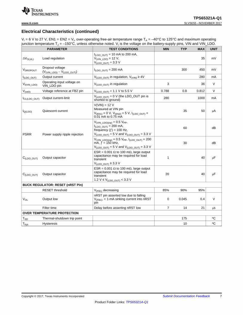
7.3.1.16 Small-Signal Model for Loop ResponseFigure 11 shows an equivalent model for the buck-regulator control loop which can be modeled in a circuit-simulation program to check frequency response and dynamic load response. The error amplifier is atransconductance amplifier with a gmea of 310 μS. Model the error amplifier using an ideal voltage-controlledcurrent source. Resistor, RO, and capacitor, CO, model the open-loop gain and frequency response of theamplifier. The 1-mV AC-voltage source between nodes a and b effectively breaks the control loop for thefrequency-response measurements. Plotting c versus a shows the small-signal response of the frequencycompensation. Plotting a versus b shows the small-signal response of the overall loop. Check the dynamic loopresponse by replacing RL with a current source that has the appropriate load-step amplitude and step rate in atime-domain analysis. This equivalent model is only valid for continuous-conduction-mode designs.

VO
Vref = 0.8 V
COMP
FB1
ErrorAmplifier
gmea310 µA/V
+
±
SWPower Stage
gmps = 10.5 A/V
c
R3RO_ea
R1
R1
RESRRL
a
b
C2
C1
CO_ea
CO
17
TPS65321A-Q1www.ti.com SLVSE55 –NOVEMBER 2017
Product Folder Links: TPS65321A-Q1
Submit Documentation FeedbackCopyright © 2017, Texas Instruments Incorporated
Feature Description (continued)
Figure 11. Small-Signal Model for Loop Response
7.3.1.17 Simple Small-Signal Model for Peak-Current Mode ControlFigure 12 shows a simple small-signal model that can be used to understand how to design the frequencycompensation. A voltage-controlled current source (duty cycle modulator) supplying current to the outputcapacitor and load resistor can approximate the TPS65321A-Q1 buck regulator power stage. Equation 6 showsthe control-to-output transfer function, which consists of a DC gain, one dominant pole, and one ESR zero. Thequotient of the change in switch current divided by the change in COMP pin voltage (node c in Figure 11) is thepower-stage transconductance. The gmps for the TPS65321A-Q1 buck regulator power-stage is 10.5 A/V. UseEquation 7 to calculate the low-frequency gain of the power stage which is the product of the transconductanceand the load resistance.
As the load current increases and decreases, the low-frequency gain decreases and increases, respectively. Thisvariation with the load seems problematic at first, but the dominant pole moves with the load current (seeEquation 8). The dashed line in the right half of Figure 12 highlights the combined effect. As the load currentdecreases, the gain increases and the pole frequency lowers, keeping the 0-dB crossover frequency the samefor the varying load conditions, which makes designing the frequency compensation easier. The type of outputcapacitor chosen determines whether the ESR zero has a profound effect on the frequency compensationdesign. Using high-ESR aluminum-electrolytic capacitors can reduce the number of frequency-compensationcomponents required to stabilize the overall loop because the phase margin increases from the ESR zero at thelower frequencies (see Equation 9).
Z _ modESR O
1ƒ
2π R C=
´ ´
P _ modL O
1ƒ
2π R C=
´ ´
dc ps LA gm R= ´
ZOdc
C
P
s1
2π ƒVA
V s1
2π ƒ
æ ö+ç ÷
´è ø= ´æ ö
+ç ÷´è ø
VO
gmps = 10.5 A/V
VCAdc
¦P
¦Z
RESR
RL
CO
18
TPS65321A-Q1SLVSE55 –NOVEMBER 2017 www.ti.com
Product Folder Links: TPS65321A-Q1
Submit Documentation Feedback Copyright © 2017, Texas Instruments Incorporated
Feature Description (continued)
Figure 12. Simple Small-Signal Model and Frequency Response for Peak-Current Mode
(6)
(7)
(8)
(9)
7.3.1.18 Small-Signal Model for Frequency CompensationThe buck regulator of the TPS65321A-Q1 device uses a transconductance amplifier as the error amplifier.Figure 13 shows compensation circuits. Implementation of Type 2 circuits is most likely in high-bandwidth power-supply designs. The purpose of loop compensation is to ensure stable operation while maximizing dynamicperformance. Use of the Type 1 circuit is with power-supply designs that have high-ESR aluminum electrolytic ortantalum capacitors. Equation 10 and Equation 11 show how to relate the frequency response of the amplifier tothe small-signal model in Figure 13. Modeling of the open-loop gain and bandwidth uses RO and CO shown inFigure 13. See the Typical Application section for a design example with a Type 2A network that has a low-ESRoutput capacitor. For stability purposes, the target must have a loop-gain slope that is –20 dB/decade at thecrossover frequency. Also, the crossover frequency must not exceed one-fifth of the switching frequency (120kHz in the case of a 600-kHz switching frequency).
For dynamic purposes, the higher the bandwidth, the faster the load-transient response. A large DC gain meanshigh DC-regulation accuracy (DC voltage changes little with load or line variations). To achieve this loop gain, setthe compensation components according to the shape of the control-output bode plot.
Equation 10 through Equation 20 serve as a reference to calculate the compensation components. RO and C1form the dominant pole (P1). A resistor (R3) and a capacitor (C1) in series to ground work as zero (Z1). Inaddition, add a lower-value capacitor (C2) in parallel with R3 to work as an optional pole. This capacitor can filternoise at switching frequency, and is also required if the output capacitor has high ESR.

ea O _ ea
R2A0 gm R
R1 R2= ´ ´
+
Z1
P1 P2
21
2π ƒEA A0
2 21 1
2π ƒ 2π ƒ
æ ö+ç ÷
´è ø= ´æ ö æ ö
+ ´ +ç ÷ ç ÷´ ´è ø è ø
O _ ea O _ ea
1P0
2π R C=
´ ´
eaO _ ea
gmC
2π BW (Hz)=
´
olO _ ea
ea
A (V/V)R
gm=
Aol
P1
P2
P0
Z1
A0
A1
BW
VO
Vref = 0.8 V
COMP
FB1
ErrorAmplifier
Inside TPS65321-Q1
Type 2Agmea
Type 2B Type 1
+
±
R1
R2
CORO
C1
R3
C2
R3
C1
C2
Copyright © 2017, Texas Instruments Incorporated
19
TPS65321A-Q1www.ti.com SLVSE55 –NOVEMBER 2017
Product Folder Links: TPS65321A-Q1
Submit Documentation FeedbackCopyright © 2017, Texas Instruments Incorporated
Feature Description (continued)
Figure 13. Types of Frequency Compensation
Figure 14. Frequency Response of the Type 2 Frequency Compensation
(10)
(11)
(12)
(13)
(14)

Hysteresis
VI (V)
ON
OFF
8.5 9
O _ ea
1P2 Type 1
2π R C2=
´ ´
O _ ea
1P2 Type 2B
2π R3 C=
´ ´
1P2 Type 2A
2π R3 C2=
´ ´
1Z1
2π R3 C1=
´ ´
O _ ea
1P1
2π R C1=
´ ´
ea O _ ea
R2A1 gm R || R3
R1 R2= ´ ´
+
20
TPS65321A-Q1SLVSE55 –NOVEMBER 2017 www.ti.com
Product Folder Links: TPS65321A-Q1
Submit Documentation Feedback Copyright © 2017, Texas Instruments Incorporated
Feature Description (continued)
(15)
(16)
(17)
(18)
(19)
(20)
7.3.2 LDO RegulatorThe LDO regulator on the TPS65321A-Q1 device can be used to supply low power consumption rails. Thequiescent current in standby mode is about 35 µA under typical operating condition.
The LDO regulator require both supplies from VIN and VIN_LDO to function. The current capability of the LDOregulator is 280 mA under the full VIN_LDO input range, while V(VIN) ≥ 4 V. When VIN becomes less than 4 V,the current capability of the LDO regulator decreases.
7.3.2.1 Charge-Pump OperationThe LDO regulator has an internal charge-pump that turns on or off depending on the input voltage. The charge-pump switching circuitry does not cause conducted emissions to exceed required thresholds on the input voltageline. The charge-pump switching thresholds are hysteretic. Figure 15 shows the typical switching thresholds forthe charge pump.
Figure 15. Charge-Pump Switching Thresholds
Table 1. Typical Quiescent Current ConsumptionCHARGE PUMP ON CHARGE PUMP OFF
LDO IQ 300-µA 35 µA
7.3.2.2 Low-Voltage TrackingAt low input voltages, the regulator drops out of regulation, and the output voltage tracks input minus a drop outvoltage (VDROPOUT). This feature allows for a smaller input capacitor and can possibly eliminate the need to use aboost convertor during cold-crank conditions.

(LDO _ OUT)V 0.8 (V)R5 R6
0.8 (V)
-
= ´
21
TPS65321A-Q1www.ti.com SLVSE55 –NOVEMBER 2017
Product Folder Links: TPS65321A-Q1
Submit Documentation FeedbackCopyright © 2017, Texas Instruments Incorporated
7.3.2.3 Adjusting the Output VoltageA resistor divider from the output node to the FB2 pin sets the output voltage. TI recommends using 1%tolerance or better divider resistors. Referring to the schematics in Figure 16, begin with 10 kΩ as the selectedvalue for the R6 resistor and use Equation 21 to calculate the value of the R5 resistor.
(21)
To improve efficiency at light loads, consider using larger-value resistors. If the values are too high, the regulatoris more susceptible to noise, and voltage errors from the FB2 input current are noticeable.
7.3.3 Thermal ShutdownThe device implements an internal thermal shutdown as protection if the junction temperature exceeds 170°C(typical). The thermal shutdown forces the buck regulator to stop switching and disables the LDO regulator whenthe junction temperature exceeds the thermal trip threshold. Once the junction temperature decreases below160°C (typical), the device re-initiates the power-up sequence.
7.3.4 Enable and Undervoltage LockoutThe TPS65321A-Q1 device enable pins (EN1 and EN2) are high-voltage-tolerant input pins with an internalpulldown circuit. A high input activates the device and turns on the regulators.
The TPS65321A-Q1 device has an internal UVLO circuit to shut down the output if the input voltage falls belowan internally-fixed UVLO-falling threshold level. This UVLO circuit ensures that both regulators are not latchedinto an unknown state during low-input-voltage conditions. The regulators power up when the input voltageexceeds the UVLO-rising threshold level.
7.4 Device Functional ModesThe device has two hardware-enable pins as listed in Table 2. The EN1 pin enables and disables the buckregulator, and the EN2 pin enables and disables the LDO regulator.
Table 2. Device Operation ModesBUCK
REGULATORLDO
REGULATOR DESCRIPTIONEN1 EN2
0 0 Both the buck regulator and the LDO regulator are disabled.0 1 The buck regulator is disabled. The LDO regulator is enabled.1 0 The buck regulator is enabled and the LDO regulator is disabled.1 1 Both the buck regulator and the LDO regulator are enabled.

GND
SW
BOOTVIN
RT/CLK
SS
Supply
RST
FB1EN2
5 V
COMP
TPS65321-Q1
EN1
PowerPAD
VI = 6 V to 36 V
LDO_OUTVIN_LDO
FB2
C8100 F
R447 k
C63.3 nF
R322 k
R595.3 k
R618 k
C14.7 nF
C710 F
C2 (Optional)12 pF
D1
3.3 V
R210 k
R131.6 k
C30.1 F
L13.3 H
C447 F
C547 F
VIO
R710 k
Supply
VI = 6 V to 36 V
C94.7 F
Copyright © 2017, Texas Instruments Incorporated
22
TPS65321A-Q1SLVSE55 –NOVEMBER 2017 www.ti.com
Product Folder Links: TPS65321A-Q1
Submit Documentation Feedback Copyright © 2017, Texas Instruments Incorporated
8 Application and Implementation
NOTEInformation in the following applications sections is not part of the TI componentspecification, and TI does not warrant its accuracy or completeness. TI’s customers areresponsible for determining suitability of components for their purposes. Customers shouldvalidate and test their design implementation to confirm system functionality.
8.1 Application InformationThe TPS65321A-Q1 buck regulator operates with a supply voltage of 3.6 V to 36 V. The TPS65321A-Q1 LDOregulator operates with a supply voltage of 3 V to 36 V V. To reduce power dissipation, TI recommends to usethe output voltage of the buck regulator as the input supply for the LDO regulator. To use the output voltage ofthe buck regulator in this way, the selected buck-regulator output voltage must be higher than the selected LDO-regulator output voltage.
To optimize the switching performance (such as low jitter) in automotive applications with input voltages thathave wide ranges, TI recommends to operate the device at higher frequencies, such as 2 MHz, which also helpsachieve AM-band compliance requirements (that extends until 1.7 MHz).
8.2 Typical Application
8.2.1 2-MHzSwitching Frequency, 9-V to 16-V Input, 3.3-V Output Buck Regulator, 5-V Output LDORegulator
This example details the design of a high-frequency switching regulator and linear regulator using ceramic outputcapacitors.
Figure 16. TPS65321A-Q1 Design Example With 2-MHz Switching Frequency

I O OO
O IND I S
V max V VL min
I K V max ƒ
-
= ´
´ ´
23
TPS65321A-Q1www.ti.com SLVSE55 –NOVEMBER 2017
Product Folder Links: TPS65321A-Q1
Submit Documentation FeedbackCopyright © 2017, Texas Instruments Incorporated
Typical Application (continued)8.2.1.1 Design RequirementsA few parameters must be known to begin the design process. The determination of these parameters is typicallyat the system level. This example begins with the parameters listed in Table 3.
Table 3. Design RequirementsDESIGN PARAMETER EXAMPLE VALUEInput voltage, VIN1 6 V to 36 V, nominal 12 VOutput voltage, VREG1 (buck regulator) 3.3 V ± 2%Maximum output current, IO_max1 3 AMinimum output current, IO_min1 0.01 ATransient response, 0.01 A to 0.8 A 3%Output ripple voltage 1%Switching frequency, ƒSW 2 MHzInput voltage, VIN_LDO 6 V to 36 V, nominal 12 VOutput voltage, VREG2 (LDO regulator) 5 V ± 2%
8.2.1.2 Detailed Design Procedure
8.2.1.2.1 Switching Frequency Selection for the Buck Regulator
The first step is to decide on a switching frequency for the regulator. Typically, the user selects the highestswitching frequency possible because this produces the smallest solution size. The high switching frequencyallows for lower-valued inductors and smaller output capacitors compared to a power supply that switches at alower frequency. The selectable switching frequency is limited by the minimum on-time of the internal powerswitch, the input voltage, the output voltage, and the frequency-shift limitation.
Consider minimum on-time and frequency-shift protection as calculated with Equation 4 and Equation 5. To findthe maximum switching frequency for the regulator, select the lower value of the two results. Switchingfrequencies higher than these values result in pulse skipping or the lack of overcurrent protection during a shortcircuit. The typical minimum on-time, tON-min, is 100 ns for the TPS65321A-Q1 device. For this example, wherethe output voltage is 3.3 V and the maximum input voltage is 36 V, use a switching frequency of 2200 kHz. UseEquation 3 to calculate the timing resistance for a given switching frequency. The R4 resistor sets the switchingfrequency. A 2-MHz switching frequency requires a 47-kΩ resistor (see R4 in Figure 16).
8.2.1.2.2 Output Inductor Selection for the Buck Regulator
Use Equation 22 to calculate the minimum value of the output inductor. The output capacitor filters the inductorripple current. Therefore, selecting high inductor-ripple currents impacts the selection of the output capacitorbecause the output capacitor must have a ripple-current rating equal to or greater than the inductor ripplecurrent. In general, the inductor ripple value is at the discretion of the designer; however, the following guidelinescan be used to select this value. KIND is a coefficient that represents the amount of inductor ripple current relativeto the maximum output current.
(22)
For designs using low-ESR output capacitors such as ceramics, use a value as high as KIND = 0.3. When usinghigher-ESR output capacitors, KIND = 0.2 yields better results. In a wide-input voltage regulator, selecting aninductor ripple current on the larger side is best because it allows the inductor to still have a measurable ripplecurrent with the input voltage at a minimum.

OO
S O
2 IC
ƒ V
´ D>
´ D
rippleL peak O
II I
2-
= +
2 2L RMS O ripple
1I I I
12-
= +
( )O I Oripple
I o S
V V max VI
V max L ƒ
´ -=
´ ´
24
TPS65321A-Q1SLVSE55 –NOVEMBER 2017 www.ti.com
Product Folder Links: TPS65321A-Q1
Submit Documentation Feedback Copyright © 2017, Texas Instruments Incorporated
For this design example, use KIND = 0.2 and the minimum inductor value which is calculated as 2.27 µH. For thisdesign, select standard value which is 3.3 µH (see L1 in Figure 16). Use Equation 23 to calculate the inductorripple current (Iripple). For the output filter inductor, do not to exceed the RMS-current and saturation-currentratings. Use Equation 24 and Equation 25 to calculate the RMS current (IL-RMS) and the peak inductor (IL-peak).
(23)
(24)
(25)
For this design, the RMS inductor current is 3 A, the peak inductor current is 3.21 A, and the inductor ripplecurrent is 0.41 A. The selected inductor is a Coilcraft XAL4030-332ME, which has a saturation-current rating of5.5 A and an RMS-current rating of 5 A. As the equation set demonstrates, lower ripple current reduces theoutput ripple voltage of the buck regulator but requires a larger value of inductance. Selecting higher ripplecurrents increases the output ripple voltage of the buck regulator but allows for a lower inductance value.
8.2.1.2.3 Output Capacitor Selection for the Buck Regulator
Consider three primary factors when selecting the value of the output capacitor. The output capacitor determinesthe modulator pole, the output ripple voltage, and how the buck regulator responds to a large change in loadcurrent. Select the output capacitance based on the most stringent of these three criteria. The desired responseto a large change in the load current is the first criterion. The output capacitor must supply the load with currentwhen the regulator cannot. This situation occurs if the desired hold-up times are present for the buck regulator. Inthis case, the output capacitor must hold the output voltage above a certain level for a specified amount of timeafter the input power is removed. The regulator is also temporarily unable to supply sufficient output current if alarge, fast increase occurs affecting the current requirements of the load, such as a transition from no load to fullload. The buck regulator usually requires two or more clock cycles for the control loop to notice the change inload current and output voltage, and to adjust the duty cycle to react to the change. Size the output capacitor tosupply the extra current to the load until the control loop responds to the load change. The output capacitancemust be large enough to supply the difference in current for two clock cycles while only allowing a tolerableamount of droop in the output voltage. Use Equation 26 to calculate the minimum output capacitance required tosupply the difference in current.
where• ΔIO is the change in the buck-regulator output current• ƒS is the switching frequency of the buck regulator• ΔVO is the allowable change in the buck-regulator output voltage (26)
For this example, the specified transient load response is a 3% change in VO for a load step from 0.01 A to 0.8A. For this example, ΔIO = 0.8 – 0.01 = 0.79 A and ΔVO = 0.03 × 3.3 = 0.1 V. Using these numbers results in aminimum capacitance of 7.2 µF. This value does not consider the ESR of the output capacitor in the outputvoltage change. For ceramic capacitors, the ESR is usually small enough to ignore in this calculation. Aluminumelectrolytic and tantalum capacitors have higher ESR that must be take into consideration.
The catch diode of the regulator cannot sink current. Therefore any stored energy in the inductor produces anoutput-voltage overshoot when the load current rapidly decreases. Also, size the output capacitor to absorb theenergy stored in the inductor when transitioning from a high load current to a lower load current. The excessenergy that is stored in the output capacitor increases the voltage on the capacitor. Size the capacitor to maintainthe desired output voltage during these transient periods.

O I OCO(RMS)
I O S
V (V max V )I
12 V max L ƒ
´ -
<
´ ´ ´
O rippleESR
L ripple
VR
I
-
-
<
OO rippleS
L ripple
1 1C
V8 ƒ
I
-
-
> ´
´
2 2OH OL
O O 2 2f i
(I I )C L
(V V )
-
> ´
-
25
TPS65321A-Q1www.ti.com SLVSE55 –NOVEMBER 2017
Product Folder Links: TPS65321A-Q1
Submit Documentation FeedbackCopyright © 2017, Texas Instruments Incorporated
Use Equation 27 to calculate the minimum capacitance to keep the output voltage overshoot to a desired value.
where• LO is the output inductance of the buck regulator• IOH is the output current of the buck regulator under heavy load• IOL is the output current of the buck regulator under light load• Vf is the final peak output voltage of the buck regulator• Vi is the initial capacitor voltage of the buck regulator (27)
For this example, the worst-case load step is from 3 A to 0.01 A. The output voltage increases during this loadtransition, and the stated maximum in the specification is 3% of the output voltage (see the ElectricalCharacteristics table). This makes Vf = 1.03 × 3.3 = 3.4 Vi is the initial capacitor voltage, which is the nominaloutput voltage of 3.3 V. Using these numbers in Equation 27 yields a minimum capacitance of 30 µF.
Equation 28 calculates the minimum output capacitance needed to meet the output ripple-voltage specification.Equation 28 yields 0.8 µF.
where• VO-ripple is the maximum allowable output ripple voltage of the buck regulator• IL-ripple is the inductor ripple current of the buck regulator (28)
Use Equation 29 to calculate the maximum ESR required for the output capacitor to meet the output voltageripple specification. As a result of Equation 29, the ESR should be less than 80 mΩ.
(29)
The most stringent criterion for the output capacitor is 30 µF of capacitance to keep the output voltage inregulation during a load transient.
Factor in additional capacitance deratings for aging, temperature, and DC bias which increase this minimumvalue. For this example, two 47-µF, 25-V ceramic capacitors with 3 mΩ of ESR are used (see C4 and C5 inFigure 16). Capacitors generally have limits to the amount of ripple current they can handle without failing orproducing excess heat. Specify an output capacitor that can support the inductor ripple current. Some capacitordata sheets specify the root-mean-square (RMS) value of the maximum ripple current.
Use Equation 30 to calculate the RMS ripple current that the output capacitor must support. For this application,Equation 30 yields 119 mA.
(30)
8.2.1.2.4 Catch Diode Selection for the Buck Regulator
The TPS65321A-Q1 device requires an external catch diode between the SW pin and GND (see D1 inFigure 16). The selected diode must have a reverse voltage rating equal to or greater than VImax. The peakcurrent rating of the diode must be greater than the maximum inductor current. The diode should also have a lowforward voltage. Schottky diodes are typically a good choice for the catch diode because of low forward voltageof these diodes. The lower the forward voltage of the diode, the higher the efficiency of the regulator.
Typically, the higher the voltage and current ratings the diode has, the higher the forward voltage is. Although thedesign example has an input voltage up to 36 V, select a diode with a minimum of 40-V reverse voltage to allowinput voltage transients up to the rated voltage of the TPS65321A-Q1 device.

O Oss
O(avg)
C V 0.8t
I
´ ´
>
OI
I S
I max 0.25V
C ƒ
´D =
´
O I OCI(RMS) O
I I
V (V min V )I I max
V min V min
-
= ´ ´
26
TPS65321A-Q1SLVSE55 –NOVEMBER 2017 www.ti.com
Product Folder Links: TPS65321A-Q1
Submit Documentation Feedback Copyright © 2017, Texas Instruments Incorporated
For the example design, the selection of a Schottky diode is SL44-E3/57 based on the low forward voltage of thisdiode. This diode is also available in a larger package size, which has better thermal characteristics. The typicalforward voltage of the SL44-E3/57 is 0.44 V.
Also, select a diode with an appropriate power rating. The diode conducts the output current during the off-timeof the internal power switch. The off-time of the internal switch is a function of the maximum input voltage, theoutput voltage, and the switching frequency. The output current during the off-time, multiplied by the forwardvoltage of the diode, equals the conduction losses of the diode. At higher switching frequencies, consider the AClosses of the diode. The AC losses of the diode are because the charging and discharging of the junctioncapacitance and reverse recovery.
8.2.1.2.5 Input Capacitor Selection for the Buck Regulator
The TPS65321A-Q1 device requires a high-quality ceramic input decoupling capacitor (type X5R or X7R) of atleast 3 µF of effective capacitance, and in some applications a bulk capacitance. The effective capacitanceincludes any DC bias effects. The voltage rating of the input capacitor must be greater than the maximum inputvoltage. The capacitor must also have a ripple-current rating greater than the maximum input-current ripple of theTPS65321A-Q1 device. Use Equation 31 to calculate the input ripple current (ICI(RMS)).
The value of a ceramic capacitor varies significantly over temperature and the amount of DC bias applied to thecapacitor. Minimize the capacitance variations because of temperature by selecting a dielectric material that isstable over temperature. Designers usually select X5R and X7R ceramic dielectrics for power regulatorcapacitors because these capacitors have a high capacitance-to-volume ratio and are fairly stable overtemperature. Also, select the output capacitor with the DC bias taken into consideration. The capacitance valueof a capacitor decreases as the DC bias across a capacitor increases.
This design requires a capacitor with at least a 40-V voltage rating to support the maximum input voltage.Common standard capacitor voltage ratings include 4 V, 6.3 V, 10 V, 16 V, 25 V, 50 V, 63V, or 100 V. For thisdesign example. The selection for this example is a 100-µF, 50-V capacitor (see C8 in Figure 16).
(31)
The input-capacitance value determines the input ripple voltage of the regulator. Use Equation 32 to calculate theinput ripple voltage (ΔVI).
(32)
Using the design example values, IOmax = 3 A, CI = 100 µF, ƒS = 2200 kHz, yields an input ripple voltage of 3.4mV and an RMS input ripple current of 1.49 A.
8.2.1.2.6 Soft-Start Capacitor Selection for the Buck Regulator
The soft-start capacitor determines the minimum amount of time required for the output voltage to reach thenominal programmed value during power up which is useful if a load requires a controlled-voltage slew rate. Thisfeature is also useful if the output capacitance is large and requires large amounts of current to charge thecapacitor quickly to the output voltage level. The large currents required to charge the capacitor may make theTPS65321A-Q1 device reach the current limit, or excessive current draw from the input power supply may causethe input voltage rail to sag. Limiting the output voltage-slew rate solves both of these problems.
The soft-start time must be long enough to allow the regulator to charge the output capacitor up to the outputvoltage without drawing excessive current. Use Equation 33 to calculate the minimum soft-start time, tss, requiredto charge the output capacitor, CO, from 10% to 90% of the output voltage, VO, with an average load current ofIo(avg).
(33)
In the example, to charge the effective output capacitance of 94 µF up to 3.3 V while allowing the average outputcurrent to be 3 A requires a 0.083 ms soft-start time.

CO O O
ps ref ea
2π ƒ C VR3
gm V gm
æ ö æ ö´ ´= ´ç ÷ ç ÷ç ÷ ´è øè ø
SCO P _ mod
ƒƒ ƒ
2= ´
CO P _ mod Z _ modƒ ƒ ƒ= ´
Z _ modESR O
1ƒ
2π R C=
´ ´
maxP _ mod
L O O O
I1ƒ
2π R C 2π V C= =
´ ´ ´ ´
27
TPS65321A-Q1www.ti.com SLVSE55 –NOVEMBER 2017
Product Folder Links: TPS65321A-Q1
Submit Documentation FeedbackCopyright © 2017, Texas Instruments Incorporated
When the soft-start time is known, use Equation 2 to calculate the soft-start capacitor. For the example circuit,the soft-start time is not too critical because the output-capacitor value is 2 × 47 µF, which does not require muchcurrent to charge to 3.3 V. The example circuit has the soft-start time set to an arbitrary value of 1 ms, whichrequires a 3.125 nF soft-start capacitor. This design uses the next-larger standard value of 3.3 nF.
8.2.1.2.7 Bootstrap Capacitor Selection for the Buck Regulator
Connect a 0.1-µF ceramic capacitor between the BOOT and SW pins for proper operation. TI recommends usinga ceramic capacitor with X5R or better-grade dielectric. The capacitor should have a 10-V or higher voltagerating.
8.2.1.2.8 Output Voltage and Feedback Resistor Selection for the Buck Regulator
The voltage divider of R1 and R2 sets the output voltage. For the design example, the selected value of R2 is 10kΩ, and the calculated value of R1 is 32.1 kΩ. Because of current leakage of the FB1 pin, the current flowingthrough the feedback network should be greater than 1 μA to maintain the output-voltage accuracy. Selectinghigher resistor values decreases the quiescent current and improves efficiency at low output currents, but canintroduce noise immunity problems.
8.2.1.2.9 Frequency Compensation Selection for the Buck Regulator
Several possible methods exist to design closed loop compensation for DC-DC converters. The methodpresented here is easy to calculate and ignores the effects of the slope compensation that is internal to the buckregulator. Ignoring the slope compensation usually causes the actual crossover frequency to be lower than thecrossover frequency used in the calculations. This method assumes the crossover frequency is between themodulator pole and the ESR zero, and that the ESR zero is at least 10 times greater than the modulator pole.
To begin, use Equation 34 to calculate the modulator pole, ƒP_mod, and Equation 35 to calculate the ESR zero,ƒz_mod.
(34)
(35)
Use Equation 36 and Equation 37 to calculate an estimate starting point for the crossover frequency, ƒCO, todesign the compensation.
(36)
(37)
For the example design, ƒP_mod is 1.54 kHz and ƒZ_mod is 564 kHz. Equation 36 is the geometric mean of themodulator pole and the ESR zero and Equation 37 is the mean of the modulator pole and the switchingfrequency. Equation 36 yields 29.5 kHz and Equation 37 results 41.1 kHz. Use the lower value of Equation 36 orEquation 37 for an initial crossover frequency.
For this example, the target ƒCO value is 29.5 kHz. Next, calculate the compensation components. Use a resistorin series with a capacitor to create a compensating zero. A capacitor in parallel to these two components formsthe compensating pole.
The total loop gain, which consists of the product of the modulator gain, the feedback voltage-divider gain, andthe error amplifier gain at ƒCO equal to 1. Use Equation 38 to calculate the compensation resistor, R3 (see theschematic in Figure 16).
(38)
Assume the power-stage transconductance, gmps, is 10.5 S. The output voltage (VO), reference voltage (Vref),and amplifier transconductance, (gmea) are 3.3 V, 0.8 V, and 310 μS, respectively. The calculated value for R3 is22.1 kΩ. For this design, use a value of 22 kΩ for R3. Use Equation 39 to set the compensation zero to themodulator pole frequency.

S
1C2
π R3 ƒ=
´ ´
O ESRC RC2
R3
´
=
P _ mod
1C1
2π R3 ƒ=
´ ´
28
TPS65321A-Q1SLVSE55 –NOVEMBER 2017 www.ti.com
Product Folder Links: TPS65321A-Q1
Submit Documentation Feedback Copyright © 2017, Texas Instruments Incorporated
(39)
Equation 37 yields 4.69 nF for compensating capacitor C1 (see the schematic in Figure 16). For this design,select a value of 4.7 nF for C1.
To implement a compensation pole as needed, use an additional capacitor, C2, in parallel with the seriescombination of R3 and C1. Use Equation 40 and Equation 41 to calculate the value of C2 and select the largerresulting value to set the compensation pole. Type 2B compensation does not use C2 because it would demanda low ESR of the output capacitor.
(40)
(41)
8.2.1.2.10 LDO Regulator
Depending on the end application, use different values of external components can be used. To program theoutput voltage, carefully select the feedback resistors, R5 and R6 (see the schematic in Figure 16). Using smallerresistors results in higher current consumption, whereas using very large resistors impacts the sensitivity of theregulator. Therefore selecting feedback resistors such that the sum of R5 and R6 is between 20 kΩ and 200 kΩis recommended.
If the desired regulated output voltage is 5 V on selecting R6, the value of R5 can be calculated. With Vref = 0.8 V(typical), VO = 5 V, and selecting R6 = 18 kΩ, the calculated value of R5 is 95.3 kΩ.
An output capacitor for the LDO regulator is required (see C10 in Figure 16) to prevent the output fromtemporarily dropping down during fast load steps. TI recommends a low-ESR ceramic capacitor with dielectric oftype X5R or X7R. Additionally, a bypass capacitor can be connected at the output to decouple high-frequencynoise based on the requirements of the end application.
8.2.1.2.11 Power Dissipation
8.2.1.2.11.1 Power Dissipation Losses of the Buck Regulator
Use the following equations to calculate the power dissipation losses for the buck regulator. These losses areapplicable for continuous-conduction-mode (CCM) operation.1. Conduction loss:
PCON = IO2 × rDS(on) × (VO / VI)
where• IO is the buck regulator output current• VO is the buck regulator output voltage• VI is the input voltage (42)
2. Switching loss:PSW = ½ × VI × IO × (tr + tf) × fS
where• tr is the FET switching rise time (tr maximum = 20 ns)• tf is the FET switching fall time (tf maximum = 20 ns)• ƒS is the switching frequency of the buck regulator (43)
3. Gate drive loss:PGate = Vdrive × Qg × ƒsw
where• Vdrive is the FET gate-drive voltage (typically Vdrive = 6 V)• Qg = 1 × 10⁻⁹ (nC, typical) (44)

Pow
er D
issi
patio
n (W
)
Ambient Temperature (qC)
0.5
125 150
1
100
1.5
75
2
2.5
3
25 5000
29
TPS65321A-Q1www.ti.com SLVSE55 –NOVEMBER 2017
Product Folder Links: TPS65321A-Q1
Submit Documentation FeedbackCopyright © 2017, Texas Instruments Incorporated
8.2.1.2.12 Power Dissipation Losses of the LDO RegulatorPLDO = (VVIN_LDO – V(LDO_OUT)) × I(LDO_OUT) (45)
8.2.1.2.13 Total Device Power Dissipation Losses and Junction Temperature1. Supply loss:
PIC = VI × IQ-normal (46)2. Total power loss:
PTotal = PCON + PSW + PGate + PLDO + PIC (47)
For a given operating ambient temperature TA:TJ = TA + Rth × PTotal
where• TJ is the junction temperature in °C• TA is the ambient temperature in °C• Rth is the thermal resistance of package in (°C/W)• PTotal is the total power dissipation (W) (48)
For a given maximum junction temperature TJ-max = 150°C, the allowed Total power dissipation is given as:TA-max = TJ-max -Rth × PTotal (49)
where• TA-max is the maximum ambient temperature in °C• TJ-max is the maximum junction temperature in °C (50)
Additional power losses occur in the regulator circuit because of the inductor AC and DC losses, the Schottkydiode, and trace resistance that impact the overall efficiency of the regulator.
Figure 17 shows the thermal derating profile of the 14-pin HTSSOP Package With PowerPAD™ . It is importantto consider additional cooling strategies if necessary to maintain the junction temperature of the device below themaximum junction temperature of 150 °C.
Figure 17. Thermal Derating Profile ofTPS65321A-Q1 in 14-pin HTSSOP Package With PowerPAD

0
10
20
30
40
50
60
70
80
90
100
0.0 1.0 2.0 3.0 4.0
Effic
iency
(%)
Output Current (A)
fsw = 300kHz
fsw = 2MHz
C001
fS = 300 kHz
fS = 2 MHz
EN2
LDO_out
I_load
5 V/div
2 V/div
200 /mA div
LDO_out
I_load
50 mV/div
200 mA/div
Buck_out
I_load
200 mV/div
1 A/div
EN1
Buck_out
SS
I_load
5 V/div
1 V/div
1 V/div
200 mA/div
30
TPS65321A-Q1SLVSE55 –NOVEMBER 2017 www.ti.com
Product Folder Links: TPS65321A-Q1
Submit Documentation Feedback Copyright © 2017, Texas Instruments Incorporated
8.2.1.3 Application Curves
100 µs/div ƒS = 2 MHz Buck Output Voltage = 5 V
Figure 18. Buck Regulator Output at Load Transient(200 mA to 3 A)
1 ms/div
Figure 19. Buck-Regulator Startup Operation
400 µs/div
Figure 20. LDO Regulator Startup Operation
10 µs/div V(LDO_OUT) = 5 V
Figure 21. LDO-Regulator Output at Load Transient(50 mA to 300 mA)
Figure 22. Buck Efficiency Versus Output Current

BOOT1
VIN2
VIN_LDO3
LDO_OUT4
FB25
RST6
EN27
EN1
RT/CLK
SS
FB1
COMP
GND
SW
PW
PD
15
9 V to 18 V (40 V PK)
C510.1 F
TP_PM1GNDFB1
VIN
12
J3
3V3
GND2
12
J112
J2
GNDVCAM
GND
VIO
8
9
10
11
12
13
14
U01TPS65321QPWPRQ1
10 k
VBATTC5047 F
GND
C10.1 F
R48240 k
R5075 k
GND
3.3 V at 250 mAC61
10 FVIN
R62240 k
FSW 500 kHz
C540.01 F
C5247 nF
R5612 k
C5356 pF
FCO 8.7 kHzPM > 80 DegsGM < ±15 dB
D800B340A-13-F
GND
R5710
C57220 pF
MSS1048-103MLB
TP_SW
GND1
R5351 k
FB1 VFB 800 mV
R54360 k
GND
R5549.9
L04 33 F 6V5
6.5 V at 1 A
C601 F
C5822 F
C5922 F
C6222 F
C6322 F
Copyright © 2017, Texas Instruments Incorporated
31
TPS65321A-Q1www.ti.com SLVSE55 –NOVEMBER 2017
Product Folder Links: TPS65321A-Q1
Submit Documentation FeedbackCopyright © 2017, Texas Instruments Incorporated
8.2.2 Design Example With 500-kHz Switching Frequency
R55 is for test purposes only.
Figure 23. TPS65321A-Q1 Design Example With 500-kHz Switching Frequency
8.2.2.1 Design RequirementsThis example begins with the parameters listed in Table 4.
Table 4. Design ParametersDESIGN PARAMETER EXAMPLE VALUEInput voltage, VIN1 9 V to 18 V, typical 12 VOutput voltage, VREG1 (buck regulator) 6.5 V ± 2%Maximum output current IO_max1 1 AMinimum output current IO_min1 0.01 ATransient response 0.01 A to 1 A 3%Output ripple voltage 1%Switching frequency ƒSW 500 kHzOutput voltage, VREG2 (LDO regulator) 3.3 V ± 2%Overvoltage threshold 106% of output voltageUndervoltage threshold 91% of output voltage
8.2.2.2 Detailed Design ProcedureFor the 500-kHz switching-frequency design, make the adjustments as outlined in the following sections. Forsections such as LDO-component calculations, bootstrap-capacitor selection, and others that are not listed in thissection, see the 2-MHzSwitching Frequency, 9-V to 16-V Input, 3.3-V Output Buck Regulator, 5-V Output LDORegulator section.
8.2.2.2.1 Selecting the Switching Frequency
For 500-kHz operation, use a 240-kΩ resistor which is calculated using Equation 3. The R62 resistor sets thisswitching frequency.
8.2.2.2.2 Output Inductor Selection
Using Equation 22, the inductor value is calculated as 27.7 μH with KIND = 0.3. This design example can allow fora higher ripple current, therefore, select the nearest standard value of 33 µH. The RMS and peak inductor-current ratings are calculated using Equation 24 and Equation 25 which result in 1.00 A and 1.13 A, respectively.The value of the output-filter inductor must not exceed the RMS-current and saturation-current ratings.

32
TPS65321A-Q1SLVSE55 –NOVEMBER 2017 www.ti.com
Product Folder Links: TPS65321A-Q1
Submit Documentation Feedback Copyright © 2017, Texas Instruments Incorporated
8.2.2.2.3 Output Capacitor
For this example, the specified transient load response is a 3% change in VO for a load step from 0.01 A to 1 A(full load). For this example, ΔIO = 1 – 0.01 = 0.99 A and ΔVO = 0.03 × 6.5 = 0.195 V. Using these numbersresults in a minimum capacitance of 20.31 μF. This value does not consider the ESR of the output capacitor inthe output voltage change. For ceramic capacitors, the ESR is usually small enough to ignore in this calculation.
Aluminum electrolytic and tantalum capacitors have higher ESR that should be considered. The catch diode ofthe regulator cannot sink current, so any stored energy in the inductor produces an output-voltage overshootwhen the load current rapidly decreases. Also, size the output capacitor to absorb the energy stored in theinductor when transitioning from a high load current to a lower load current. The excess energy that is stored inthe output capacitor increases the voltage on the capacitor. Size the capacitor to maintain the desired outputvoltage during these transient periods. Use Equation 27 to calculate the minimum capacitance to keep the outputvoltage overshoot to a desired value.
For this example, the worst-case load step is from 1 A to 0.01 A. The output voltage increases during this loadtransition, and the stated maximum in our specification is 3% of the output voltage resulting in Vf = 1.03 × 6.5 =6.7. The initial capacitor voltage, Vi, is the nominal output voltage of 5 V. Using these values, Equation 27 yieldsa minimum capacitance of 3.88 μF. Equation 28 calculates the minimum output capacitance required to meet theoutput ripple-voltage specification. Equation 28 yields 10.6 μF. Equation 29 calculates the maximum ESR anoutput capacitor can have to meet the output ripple-voltage specification. Equation 29 indicates the ESR shouldbe less than 60.2 mΩ.
The most stringent criterion for the output capacitor is 20.31 μF of capacitance to keep the output voltage inregulation during a load transient.
Factor in additional capacitance deratings for aging, temperature, and DC bias which increase this minimumvalue. For this example, four 22-μF, 25-V and one 1-µF, 25-V ceramic capacitors with 10 mΩ of ESR are used.Specify an output capacitor that can support the inductor ripple current. Some capacitor data sheets specify theRMS value of the maximum ripple current. Use Equation 30 to calculate the RMS ripple current that the outputcapacitor must support. For this design example, Equation 30 yields 240 mA.
8.2.2.2.4 Compensation
This design example use a different approach for calculating compensation values, beginning with the desiredcrossover frequency. Ensure that the crossover frequency is maintained at 10 kHz to provide reasonable phasemargin (PM). To achieve circuit stability, a phase margin greater than 60 degrees and a gain margin less than 15dB is required. Next, place the zero close to the load pole. The zero is determined using C52 and R56. For thisexample, select a value of 10 kΩ for R56 which results in a value of approximately 4.7 nF for C52. The pole,resulting from C53 and R56, can be placed between 10 times the crossover frequency and 1/3 of the switchingfrequency. The gain is adjusted to be maintained over 60 degrees of phase margin and –15 dB of gain margin.The resulting value of C53 is approximately 100 pF for a pole frequency of 159 kHz.
Use the following component values:R56 = 12 kΩC53 = 56 pFC52 = 47 nF

Output Current (A)
Effi
cien
cy (
%)
0 0.2 0.4 0.6 0.8 180
82
84
86
88
90
92
94
96
98
D001
VIN = 9 VVIN = 13.8 VVIN = 18 V
33
TPS65321A-Q1www.ti.com SLVSE55 –NOVEMBER 2017
Product Folder Links: TPS65321A-Q1
Submit Documentation FeedbackCopyright © 2017, Texas Instruments Incorporated
8.2.2.3 Application Curve
Figure 24. Efficiency vs Output Current
9 Power Supply RecommendationsThe buck regulator is designed to operate from an input voltage supply range between 3.6 V and 36 V. Thelinear regulator is designed to operate from an input supply voltage up to 36 V. Both input supplies must be wellregulated. If the input supply connected to the VIN pin is located more than a few inches from the TPS65321A-Q1 converter additional bulk capacitance may be required in addition to the ceramic bypass capacitors. Anelectrolytic capacitor with a value of 100 μF is a typical choice.
10 Layout
10.1 Layout GuidelinesTI recommends the guidelines that follow for PCB layout of the TPS65321A-Q1 device.• Inductor
Use a low-EMI inductor with a ferrite-type shielded core. Other types of inductors can also be used, however,these inductors must have low-EMI characteristics and be located away from the low-power traces andcomponents in the circuit.
• Input Filter CapacitorsLocate input ceramic filter capacitors close to the VIN pin. TI recommends surface-mount capacitors tominimize lead length and reduce noise coupling.
• FeedbackRoute the feedback trace for minimum interaction with any noise sources associated with the switchingcomponents. TI recommends to place the inductor away from the feedback trace to prevent creating an EMInoise source.
• Traces and Ground PlaneAll power (high-current) traces must be as thick and short as possible. The inductor and output capacitorsmust be as close to each other as possible to reduce EMI radiated by the power traces because of highswitching currents. In a two-sided PCB, TI recommends using ground planes on both sides of the PCB tohelp reduce noise and ground loop errors. The ground connection for the input capacitors, output capacitors,and device ground should connect to this ground plane, where the connection between input capacitors andthe catch-diode is the most critical. In a multi-layer PCB, the ground plane separates the power plane (wherehigh switching currents and components are) from the signal plane (where the feedback trace andcomponents are) for improved performance. Also, arrange the components such that the switching-currentloops curl in the same direction. Place the high-current components such that during conduction the currentpath is in the same direction. This placement prevents magnetic field reversal caused by the traces betweenthe two half-cycles, and helps reduce radiated EMI.

1
2
3
4 11
12
13
14
5
6
7
10
9
8
BOOT
VIN
VIN_LDO
LDO_OUT
FB2
RST
EN2
SW
GND
COMP
FB1
SS
RT/CLK
EN1
Buck Regulator Catch Diode
Buck Regulator Output Inductor
Buck Regulator Output Capacitor VO(BUCK)
Buck Regulator
BOOT Capacitor
Input CapacitorsVI
Power Ground
LDO Regulator Output Capacitor
VO(LDO)
Buck Regulator Compensation Components
Buck Regulator Soft-Start Capacitor
Buck Regulator Switching Frequency Resistor
Buck Regulator Resistor Feedback Network
LDO Regulator
Resistor Feedback
Network
Analog Ground Trace
Analog G
round Trace
Analog Ground Trace
Exposed Thermal Pad
Area
34
TPS65321A-Q1SLVSE55 –NOVEMBER 2017 www.ti.com
Product Folder Links: TPS65321A-Q1
Submit Documentation Feedback Copyright © 2017, Texas Instruments Incorporated
10.2 Layout Example
Figure 25. TPS65321A-Q1 Layout Example
Figure 26. TPS65321A-Q1 Layout ExampleTop Side
Figure 27. TPS65321A-Q1 Layout ExampleBottom Side

35
TPS65321A-Q1www.ti.com SLVSE55 –NOVEMBER 2017
Product Folder Links: TPS65321A-Q1
Submit Documentation FeedbackCopyright © 2017, Texas Instruments Incorporated
11 Device and Documentation Support
11.1 Documentation Support
11.1.1 Related DocumentationFor related documentation see the following:• Texas Instruments, Interfacing TPS57xxx-Q1,TPS65320-Q1 Family, and TPS65321-Q1 Devices With Low
Impendence External Clock Drivers application report• Texas Instruments, Low Quiescent Current with Asynchronous Buck Converters at High Temperatures
application report• Texas Instruments, TPS65321EVM (HVL125A) User Guide• Texas Instruments, TPS65321-Q1 Design Checklist
11.2 Receiving Notification of Documentation UpdatesTo receive notification of documentation updates, navigate to the device product folder on ti.com. In the upperright corner, click on Alert me to register and receive a weekly digest of any product information that haschanged. For change details, review the revision history included in any revised document.
11.3 Community ResourcesThe following links connect to TI community resources. Linked contents are provided "AS IS" by the respectivecontributors. They do not constitute TI specifications and do not necessarily reflect TI's views; see TI's Terms ofUse.
TI E2E™ Online Community TI's Engineer-to-Engineer (E2E) Community. Created to foster collaborationamong engineers. At e2e.ti.com, you can ask questions, share knowledge, explore ideas and helpsolve problems with fellow engineers.
Design Support TI's Design Support Quickly find helpful E2E forums along with design support tools andcontact information for technical support.
11.4 TrademarksPowerPAD, E2E are trademarks of Texas Instruments.All other trademarks are the property of their respective owners.
11.5 Electrostatic Discharge CautionThis integrated circuit can be damaged by ESD. Texas Instruments recommends that all integrated circuits be handled withappropriate precautions. Failure to observe proper handling and installation procedures can cause damage.
ESD damage can range from subtle performance degradation to complete device failure. Precision integrated circuits may be moresusceptible to damage because very small parametric changes could cause the device not to meet its published specifications.
11.6 GlossarySLYZ022 — TI Glossary.
This glossary lists and explains terms, acronyms, and definitions.
12 Mechanical, Packaging, and Orderable InformationThe following packaging information and addendum reflect the most current data available for the designateddevices. This data is subject to change without notice and revision of this document.

PACKAGE OPTION ADDENDUM
www.ti.com 10-Dec-2020
Addendum-Page 1
PACKAGING INFORMATION
Orderable Device Status(1)
Package Type PackageDrawing
Pins PackageQty
Eco Plan(2)
Lead finish/Ball material
(6)
MSL Peak Temp(3)
Op Temp (°C) Device Marking(4/5)
Samples
TPS65321AQPWPRQ1 ACTIVE HTSSOP PWP 14 2000 RoHS & Green NIPDAU Level-3-260C-168 HR -40 to 125 T65321A
(1) The marketing status values are defined as follows:ACTIVE: Product device recommended for new designs.LIFEBUY: TI has announced that the device will be discontinued, and a lifetime-buy period is in effect.NRND: Not recommended for new designs. Device is in production to support existing customers, but TI does not recommend using this part in a new design.PREVIEW: Device has been announced but is not in production. Samples may or may not be available.OBSOLETE: TI has discontinued the production of the device.
(2) RoHS: TI defines "RoHS" to mean semiconductor products that are compliant with the current EU RoHS requirements for all 10 RoHS substances, including the requirement that RoHS substancedo not exceed 0.1% by weight in homogeneous materials. Where designed to be soldered at high temperatures, "RoHS" products are suitable for use in specified lead-free processes. TI mayreference these types of products as "Pb-Free".RoHS Exempt: TI defines "RoHS Exempt" to mean products that contain lead but are compliant with EU RoHS pursuant to a specific EU RoHS exemption.Green: TI defines "Green" to mean the content of Chlorine (Cl) and Bromine (Br) based flame retardants meet JS709B low halogen requirements of <=1000ppm threshold. Antimony trioxide basedflame retardants must also meet the <=1000ppm threshold requirement.
(3) MSL, Peak Temp. - The Moisture Sensitivity Level rating according to the JEDEC industry standard classifications, and peak solder temperature.
(4) There may be additional marking, which relates to the logo, the lot trace code information, or the environmental category on the device.
(5) Multiple Device Markings will be inside parentheses. Only one Device Marking contained in parentheses and separated by a "~" will appear on a device. If a line is indented then it is a continuationof the previous line and the two combined represent the entire Device Marking for that device.
(6) Lead finish/Ball material - Orderable Devices may have multiple material finish options. Finish options are separated by a vertical ruled line. Lead finish/Ball material values may wrap to twolines if the finish value exceeds the maximum column width.
Important Information and Disclaimer:The information provided on this page represents TI's knowledge and belief as of the date that it is provided. TI bases its knowledge and belief on informationprovided by third parties, and makes no representation or warranty as to the accuracy of such information. Efforts are underway to better integrate information from third parties. TI has taken andcontinues to take reasonable steps to provide representative and accurate information but may not have conducted destructive testing or chemical analysis on incoming materials and chemicals.TI and TI suppliers consider certain information to be proprietary, and thus CAS numbers and other limited information may not be available for release.
In no event shall TI's liability arising out of such information exceed the total purchase price of the TI part(s) at issue in this document sold by TI to Customer on an annual basis.

TAPE AND REEL INFORMATION
*All dimensions are nominal
Device PackageType
PackageDrawing
Pins SPQ ReelDiameter
(mm)
ReelWidth
W1 (mm)
A0(mm)
B0(mm)
K0(mm)
P1(mm)
W(mm)
Pin1Quadrant
TPS65321AQPWPRQ1 HTSSOP PWP 14 2000 330.0 12.4 6.9 5.6 1.6 8.0 12.0 Q1
PACKAGE MATERIALS INFORMATION
www.ti.com 12-Feb-2019
Pack Materials-Page 1

*All dimensions are nominal
Device Package Type Package Drawing Pins SPQ Length (mm) Width (mm) Height (mm)
TPS65321AQPWPRQ1 HTSSOP PWP 14 2000 350.0 350.0 43.0
PACKAGE MATERIALS INFORMATION
www.ti.com 12-Feb-2019
Pack Materials-Page 2

www.ti.com
PACKAGE OUTLINE
C
TYP6.66.2
12X 0.65
14X 0.300.19
2X3.9
(0.15) TYP
0 - 8 0.150.05
2.5581.718
2.5481.708
4X (0.4)NOTE 5
1.2 MAX
0.25GAGE PLANE
0.750.50
(1)
A
NOTE 3
5.14.9
B 4.54.3
4X (0.05)NOTE 5
4223314/A 09/2016
PowerPAD TSSOP - 1.2 mm max heightPWP0014GPLASTIC SMALL OUTLINE
NOTES: 1. All linear dimensions are in millimeters. Any dimensions in parenthesis are for reference only. Dimensioning and tolerancing per ASME Y14.5M. 2. This drawing is subject to change without notice. 3. This dimension does not include mold flash, protrusions, or gate burrs. Mold flash, protrusions, or gate burrs shall not exceed 0.15 mm per side.4. Reference JEDEC registration MO-153.5. Features may differ and may not be present.
PowerPAD is a trademark of Texas Instruments.
TM
114
0.1 C A B
87
PIN 1 IDAREA
SEATING PLANE
0.1 C
SEE DETAIL A
DETAIL ATYPICAL
SCALE 2.400
THERMALPAD
1 14
87
15

www.ti.com
EXAMPLE BOARD LAYOUT
(5.8)
0.05 MAXALL AROUND
0.05 MINALL AROUND
14X (1.5)
14X (0.45)
12X (0.65)
(3.4)NOTE 9
(5)NOTE 9
(2.56)
(2.55)
( 0.2) TYPVIA (1.1) TYP
(1.1)TYP
(R0.05) TYP
4223314/A 09/2016
PowerPAD TSSOP - 1.2 mm max heightPWP0014GPLASTIC SMALL OUTLINE
SYMM
SYMM
SEE DETAILS
LAND PATTERN EXAMPLESCALE:10X
1
78
14
METAL COVEREDBY SOLDER MASK
SOLDER MASKDEFINED PAD
15
TM
NOTES: (continued) 6. Publication IPC-7351 may have alternate designs. 7. Solder mask tolerances between and around signal pads can vary based on board fabrication site. 8. This package is designed to be soldered to a thermal pad on the board. For more information, see Texas Instruments literature numbers SLMA002 (www.ti.com/lit/slma002) and SLMA004 (www.ti.com/lit/slma004).9. Size of metal pad may vary due to creepage requirement.
METALSOLDER MASKOPENING
NON SOLDER MASKDEFINED
SOLDER MASK DETAILSPADS 1-14
SOLDER MASKDEFINED
SOLDER MASKMETAL UNDER SOLDER MASK
OPENING

www.ti.com
EXAMPLE STENCIL DESIGN
14X (1.5)
14X (0.45)
(2.56)
(2.55)BASED ON
0.125 THICKSTENCIL
12X (0.65)
(R0.05) TYP
(5.8)
4223314/A 09/2016
PowerPAD TSSOP - 1.2 mm max heightPWP0014GPLASTIC SMALL OUTLINE
2.16 X 2.160.1752.34 X 2.330.15
2.56 X 2.55 (SHOWN)0.1252.86 X 2.850.1
SOLDER STENCILOPENING
STENCILTHICKNESS
NOTES: (continued) 10. Laser cutting apertures with trapezoidal walls and rounded corners may offer better paste release. IPC-7525 may have alternate design recommendations. 11. Board assembly site may have different recommendations for stencil design.
TM
SYMM
SYMM
1
78
14
BASED ON0.125 THICK
STENCIL
BY SOLDER MASKMETAL COVERED SEE TABLE FOR
DIFFERENT OPENINGSFOR OTHER STENCILTHICKNESSES
SOLDER PASTE EXAMPLEEXPOSED PAD
100% PRINTED SOLDER COVERAGE BY AREASCALE:10X
15

IMPORTANT NOTICE AND DISCLAIMER
TI PROVIDES TECHNICAL AND RELIABILITY DATA (INCLUDING DATASHEETS), DESIGN RESOURCES (INCLUDING REFERENCE DESIGNS), APPLICATION OR OTHER DESIGN ADVICE, WEB TOOLS, SAFETY INFORMATION, AND OTHER RESOURCES “AS IS” AND WITH ALL FAULTS, AND DISCLAIMS ALL WARRANTIES, EXPRESS AND IMPLIED, INCLUDING WITHOUT LIMITATION ANY IMPLIED WARRANTIES OF MERCHANTABILITY, FITNESS FOR A PARTICULAR PURPOSE OR NON-INFRINGEMENT OF THIRD PARTY INTELLECTUAL PROPERTY RIGHTS.These resources are intended for skilled developers designing with TI products. You are solely responsible for (1) selecting the appropriate TI products for your application, (2) designing, validating and testing your application, and (3) ensuring your application meets applicable standards, and any other safety, security, or other requirements. These resources are subject to change without notice. TI grants you permission to use these resources only for development of an application that uses the TI products described in the resource. Other reproduction and display of these resources is prohibited. No license is granted to any other TI intellectual property right or to any third party intellectual property right. TI disclaims responsibility for, and you will fully indemnify TI and its representatives against, any claims, damages, costs, losses, and liabilities arising out of your use of these resources.TI’s products are provided subject to TI’s Terms of Sale (www.ti.com/legal/termsofsale.html) or other applicable terms available either on ti.com or provided in conjunction with such TI products. TI’s provision of these resources does not expand or otherwise alter TI’s applicable warranties or warranty disclaimers for TI products.
Mailing Address: Texas Instruments, Post Office Box 655303, Dallas, Texas 75265Copyright © 2020, Texas Instruments Incorporated