Embed Size (px)
Citation preview
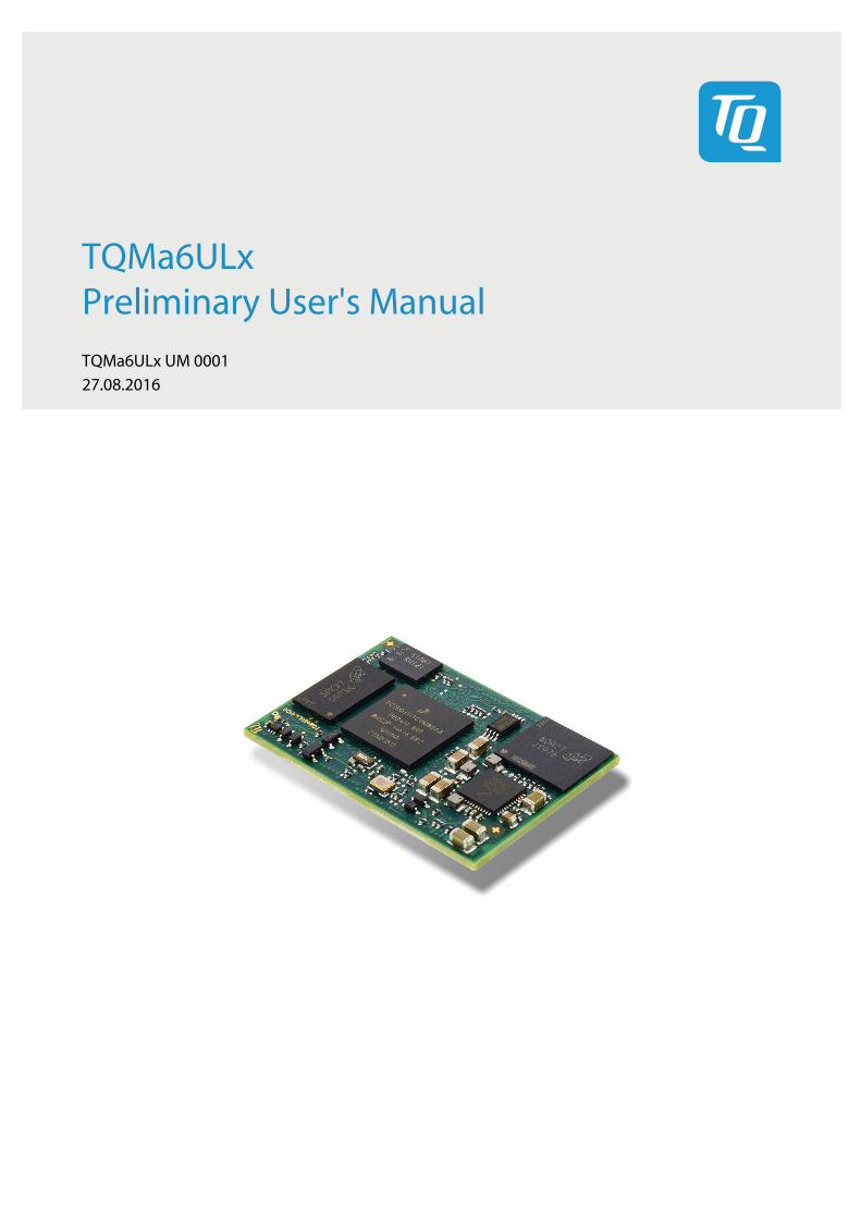
TQMa6ULx Preliminary User's Manual
TQMa6ULx UM 0001
27.08.2016
Preliminary User's Manual l TQMa6ULx UM 0001 l © 2016 TQ-Group Page i
TABLE OF CONTENTS
1. ABOUT THIS MANUAL................................................................................................................................................................................1 1.1 Copyright and license expenses.............................................................................................................................................................1 1.2 Registered trademarks ..............................................................................................................................................................................1 1.3 Disclaimer......................................................................................................................................................................................................1 1.4 Imprint............................................................................................................................................................................................................1 1.5 Tips on safety................................................................................................................................................................................................2 1.6 Symbols and typographic conventions ...............................................................................................................................................2 1.7 Handling and ESD tips...............................................................................................................................................................................2 1.8 Naming of signals .......................................................................................................................................................................................3 1.9 Further applicable documents / presumed knowledge .................................................................................................................3 2. BRIEF DESCRIPTION ....................................................................................................................................................................................4 2.1 Block diagram i.MX6ULx CPU..................................................................................................................................................................4 2.2 Key functions and characteristics...........................................................................................................................................................5 3. ELECTRONICS ...............................................................................................................................................................................................6 3.1 Interfaces to other systems and devices..............................................................................................................................................6 3.1.1 Pin multiplexing ..........................................................................................................................................................................................6 3.1.1.1 Connector X1................................................................................................................................................................................................7 3.1.1.2 Connector X2................................................................................................................................................................................................8 3.2 System components ..................................................................................................................................................................................9 3.2.1 i.MX6ULx CPU...............................................................................................................................................................................................9 3.2.1.1 CPU derivatives............................................................................................................................................................................................9 3.2.1.2 CPU errata......................................................................................................................................................................................................9 3.2.1.3 Boot modes...................................................................................................................................................................................................9 3.2.1.4 Boot configuration................................................................................................................................................................................... 10 3.2.1.5 Boot interfaces .......................................................................................................................................................................................... 10 3.2.1.6 Boot device eMMC................................................................................................................................................................................... 11 3.2.1.7 Boot device QSPI NOR flash .................................................................................................................................................................. 12 3.2.1.8 Boot device SD card ................................................................................................................................................................................ 13 3.2.2 Memory....................................................................................................................................................................................................... 14 3.2.2.1 DDR3L SDRAM .......................................................................................................................................................................................... 14 3.2.2.2 eMMC NAND flash ................................................................................................................................................................................... 15 3.2.2.3 QSPI NOR flash .......................................................................................................................................................................................... 15 3.2.2.4 EEPROM....................................................................................................................................................................................................... 16 3.2.3 RTC................................................................................................................................................................................................................ 17 3.2.4 Temperature sensor ................................................................................................................................................................................ 17 3.2.5 Interfaces .................................................................................................................................................................................................... 18 3.2.5.1 Overview..................................................................................................................................................................................................... 18 3.2.5.2 ECSPI - Enhanced Configurable SPI .................................................................................................................................................... 19 3.2.5.3 ENET – Fast Ethernet .............................................................................................................................................................................. 19 3.2.5.4 CAN – FLEXCAN ........................................................................................................................................................................................ 20 3.2.5.5 GPIO ............................................................................................................................................................................................................. 20 3.2.5.6 I2C .................................................................................................................................................................................................................. 21 3.2.5.7 eLCDIF – Enhanced LCD Interface ...................................................................................................................................................... 21 3.2.5.8 SJC – System JTAG Controller .............................................................................................................................................................. 22 3.2.5.9 TAMPER ....................................................................................................................................................................................................... 22 3.2.5.10 UART............................................................................................................................................................................................................. 23 3.2.5.11 USB ............................................................................................................................................................................................................... 24 3.2.5.12 USDHC – Ultra-Secured Digital Host Controller ............................................................................................................................ 24 3.2.5.13 XTAL – differential clock......................................................................................................................................................................... 24 3.2.6 Reset signals .............................................................................................................................................................................................. 25 3.2.7 Power supply............................................................................................................................................................................................. 26 3.2.7.1 TQMa6ULx power supply ...................................................................................................................................................................... 26 3.2.7.2 TQMa6ULx power consumption ......................................................................................................................................................... 26 3.2.7.3 Voltage monitoring ................................................................................................................................................................................. 26 3.2.7.4 Power-Up sequence TQMa6ULx / carrier board............................................................................................................................. 27 3.2.7.5 Power modes............................................................................................................................................................................................. 27 3.2.7.6 PMIC ............................................................................................................................................................................................................. 28
Preliminary User's Manual l TQMa6ULx UM 0001 l © 2016 TQ-Group Page ii
TABLE OF CONTENTS (continued)
4. MECHANICS ............................................................................................................................................................................................... 29 4.1 Connectors................................................................................................................................................................................................. 29 4.2 Dimensions ................................................................................................................................................................................................ 30 4.3 Component placement.......................................................................................................................................................................... 31 4.4 Adaptation to the environment .......................................................................................................................................................... 32 4.5 Protection against external effects..................................................................................................................................................... 32 4.6 Thermal management............................................................................................................................................................................ 32 4.7 Structural requirements......................................................................................................................................................................... 32 4.8 Notes of treatment .................................................................................................................................................................................. 32 5. SOFTWARE.................................................................................................................................................................................................. 32 6. SAFETY REQUIREMENTS AND PROTECTIVE REGULATIONS......................................................................................................... 33 6.1 EMC............................................................................................................................................................................................................... 33 6.2 ESD................................................................................................................................................................................................................ 33 6.3 Operational safety and personal security......................................................................................................................................... 33 6.4 Climatic and operational conditions.................................................................................................................................................. 34 6.5 Shock and Vibration ................................................................................................................................................................................ 35 6.6 Reliability and service life ...................................................................................................................................................................... 35 7. ENVIRONMENT PROTECTION................................................................................................................................................................ 36 7.1 RoHS............................................................................................................................................................................................................. 36 7.2 WEEE ............................................................................................................................................................................................................ 36 7.3 REACH.......................................................................................................................................................................................................... 36 7.4 EuP................................................................................................................................................................................................................ 36 7.5 Battery ......................................................................................................................................................................................................... 36 7.6 Packaging ................................................................................................................................................................................................... 36 7.7 Other entries.............................................................................................................................................................................................. 36 8. APPENDIX ................................................................................................................................................................................................... 37 8.1 Acronyms and definitions ..................................................................................................................................................................... 37 8.2 References.................................................................................................................................................................................................. 37
Preliminary User's Manual l TQMa6ULx UM 0001 l © 2016 TQ-Group Page iii
TABLE DIRECTORY
Table 1: Terms and conventions .....................................................................................................................................................................2 Table 2: Pinout connector X1...........................................................................................................................................................................7 Table 3: Pinout connector X2...........................................................................................................................................................................8 Table 4: CPU derivatives ....................................................................................................................................................................................9 Table 5: Boot modes and BT_FUSE_SEL........................................................................................................................................................9 Table 6: General boot settings...................................................................................................................................................................... 10 Table 7: Boot configuration eMMC at USDHC2....................................................................................................................................... 11 Table 8: USDHC2 mode eMMC ..................................................................................................................................................................... 11 Table 9: Boot configuration QSPI NOR flash at QSPI1............................................................................................................................ 12 Table 10: Boot configuration SD card at USDHC1..................................................................................................................................... 13 Table 11: USDHC1 SD card modes................................................................................................................................................................. 13 Table 12: i.MX6ULx SDRAM interface............................................................................................................................................................ 14 Table 13: DDR3L SDRAM................................................................................................................................................................................... 14 Table 14: eMMC NAND flash............................................................................................................................................................................ 15 Table 15: QSPI NOR flash................................................................................................................................................................................... 15 Table 16: EEPROM ............................................................................................................................................................................................... 16 Table 17: TQMa6ULx specific data in the EEPROM ................................................................................................................................... 16 Table 18: Temperature sensor......................................................................................................................................................................... 17 Table 19: Internal interfaces............................................................................................................................................................................. 18 Table 20: External interfaces............................................................................................................................................................................ 18 Table 21: Signals ECSPI2.................................................................................................................................................................................... 19 Table 22: Signals RMII......................................................................................................................................................................................... 19 Table 23: Signals FLEXCAN............................................................................................................................................................................... 20 Table 24: Signals GPIO ....................................................................................................................................................................................... 20 Table 25: Signals I2C............................................................................................................................................................................................ 21 Table 26: I2C address assignment................................................................................................................................................................... 21 Table 27: Signals LCD......................................................................................................................................................................................... 21 Table 28: JTAG modes........................................................................................................................................................................................ 22 Table 29: Signals JTAG ....................................................................................................................................................................................... 22 Table 30: Signals TAMPER................................................................................................................................................................................. 22 Table 31: Signals UART ...................................................................................................................................................................................... 23 Table 32: Signals USB_OTG .............................................................................................................................................................................. 24 Table 33: Signals USDHC1 ................................................................................................................................................................................ 24 Table 34: Signals XTAL....................................................................................................................................................................................... 24 Table 35: Signals Reset ...................................................................................................................................................................................... 25 Table 36: Parameter TQMa6ULx power consumption............................................................................................................................. 26 Table 37: Plug connectors on the TQMa6ULx ............................................................................................................................................ 29 Table 38: Suitable carrier board mating plug connectors ...................................................................................................................... 29 Table 39: Climate and operational conditions extended temperature range –25 °C to +85 °C ................................................. 34 Table 40: Climate and operational conditions industrial temperature range –40 °C to +85 °C.................................................. 34 Table 41: Shock resistance................................................................................................................................................................................ 35 Table 42: Vibration resistance ......................................................................................................................................................................... 35 Table 43: Acronyms ............................................................................................................................................................................................ 37 Table 44: Further applicable documents ..................................................................................................................................................... 37
Preliminary User's Manual l TQMa6ULx UM 0001 l © 2016 TQ-Group Page iv
ILLUSTRATION DIRECTORY
Illustration 1: Block diagram i.MX6ULx CPU...........................................................................................................................................................4 Illustration 2: Block diagram TQMa6ULx (simplified)..........................................................................................................................................6 Illustration 3: Block diagram DDR3L SDRAM interface.................................................................................................................................... 14 Illustration 4: Block diagram eMMC interface .................................................................................................................................................... 15 Illustration 5: Block diagram QSPI NOR flash interface.................................................................................................................................... 15 Illustration 6: Block diagram EEPROM interface ................................................................................................................................................ 16 Illustration 7: Block diagram RTC............................................................................................................................................................................ 17 Illustration 8: Block diagram temperature sensor interface .......................................................................................................................... 17 Illustration 9: Block diagram UART interfaces .................................................................................................................................................... 23 Illustration 10: Block diagram Reset ........................................................................................................................................................................ 25 Illustration 11: Block diagram TQMa6ULx power supply.................................................................................................................................. 26 Illustration 12: Block diagram power supply carrier board .............................................................................................................................. 27 Illustration 13: Block diagram PMIC interface....................................................................................................................................................... 28 Illustration 14: Height of TQMa6ULx ....................................................................................................................................................................... 30 Illustration 15: Overall dimensions (top view)...................................................................................................................................................... 30 Illustration 16: Top view through PCB .................................................................................................................................................................... 30 Illustration 17: Component placement top........................................................................................................................................................... 31 Illustration 18: Component placement bottom................................................................................................................................................... 31
REVISION HISTORY
Rev. Date Name Pos. Modification
0001 27.08.2016 Petz First issue
Preliminary User's Manual l TQMa6ULx UM 0001 l © 2016 TQ-Group Page 1
1. ABOUT THIS MANUAL
1.1 Copyright and license expenses
Copyright protected © 2016 by TQ-Systems GmbH.
This Preliminary User's Manual may not be copied, reproduced, translated, changed or distributed, completely or partially in electronic, machine readable, or in any other form without the written consent of TQ-Systems GmbH.
The drivers and utilities for the components used as well as the BIOS are subject to the copyrights of the respective manufacturers. The licence conditions of the respective manufacturer are to be adhered to.
Bootloader-licence expenses are paid by TQ-Systems GmbH and are included in the price.
Licence expenses for the operating system and applications are not taken into consideration and must be separately calculated / declared.
1.2 Registered trademarks
TQ-Systems GmbH aims to adhere to the copyrights of all the graphics and texts used in all publications, and strives to use original or license-free graphics and texts.
All the brand names and trademarks mentioned in the publication, including those protected by a third party, unless specified otherwise in writing, are subjected to the specifications of the current copyright laws and the proprietary laws of the present registered proprietor without any limitation. One should conclude that brand and trademarks are rightly protected by of a third party.
1.3 Disclaimer
TQ-Systems GmbH does not guarantee that the information in this Preliminary User's Manual is up-to-date, correct, complete or of good quality. Nor does TQ-Systems GmbH assume guarantee for further usage of the information. Liability claims against TQ-Systems GmbH, referring to material or non-material related damages caused, due to usage or non-usage of the information given in the Preliminary User's Manual, or due to usage of erroneous or incomplete information, are exempted, as long as there is no proven intentional or negligent fault of TQ-Systems GmbH.
TQ-Systems GmbH explicitly reserves the rights to change or add to the contents of this Preliminary User's Manual or parts of it without special notification.
1.4 Imprint
TQ-Systems GmbH
Gut Delling, Mühlstraße 2
D-82229 Seefeld
Tel: +49 (0) 8153 9308–0
Fax: +49 (0) 8153 9308–4223
Email: [email protected]
Web: http://www.tq-group.com/
Preliminary User's Manual l TQMa6ULx UM 0001 l © 2016 TQ-Group Page 2
1.5 Tips on safety
Improper or incorrect handling of the product can substantially reduce its life span.
1.6 Symbols and typographic conventions
Table 1: Terms and conventions
Symbol Meaning
This symbol represents the handling of electrostatic-sensitive modules and / or components. These components are often damaged / destroyed by the transmission of a voltage higher than about 50 V. A human body usually only experiences electrostatic discharges above approximately 3,000 V.
This symbol indicates the possible use of voltages higher than 24 V.
Please note the relevant statutory regulations in this regard.
Non-compliance with these regulations can lead to serious damage to your health and may damage or destroy the component.
This symbol indicates a possible source of danger.
Ignoring the instructions described can cause health damage, or damage the hardware.
This symbol represents important details or aspects for working with TQ-products.
Command A font with fixed-width is used to denote commands, contents, file names, or menu items.
1.7 Handling and ESD tips
General handling of your TQ-products
The TQ-product may only be used and serviced by certified personnel who have taken note of the information, the safety regulations in this document and all related rules and regulations.
A general rule is not to touch the TQ-product during operation. This is especially important when switching on, changing jumper settings or connecting other devices without ensuring beforehand that the power supply of the system has been switched off.
Violation of this guideline may result in damage / destruction of the TQMa6ULx and be dangerous to your health.
Improper handling of your TQ-product would render the guarantee invalid.
Proper ESD handling
The electronic components of your TQ-product are sensitive to electrostatic discharge (ESD).
Always wear antistatic clothing, use ESD-safe tools, packing materials etc., and operate your TQ-product in an ESD-safe environment. Especially when you switch modules on, change jumper settings, or connect other devices.

Preliminary User's Manual l TQMa6ULx UM 0001 l © 2016 TQ-Group Page 3
1.8 Naming of signals
A hash mark (#) at the end of the signal name indicates a low-active signal.
Example: RESET#
If a signal can switch between two functions and if this is noted in the name of the signal, the low-active function is marked with a hash mark and shown at the end.
Example: C / D#
If a signal has multiple functions, the individual functions are separated by slashes when they are important for the wiring.
The identification of the individual functions follows the above conventions.
Example: WE2# / OE#
1.9 Further applicable documents / presumed knowledge
• Specifications and manual of the modules used:
These documents describe the service, functionality and special characteristics of the module used (incl. BIOS).
• Specifications of the components used:
The manufacturer's specifications of the components used, for example CompactFlash cards, are to be taken note of. They contain, if applicable, additional information that must be taken note of for safe and reliable operation. These documents are stored at TQ-Systems GmbH.
• Chip errata:
It is the user's responsibility to make sure all errata published by the manufacturer of each component are taken note of. The manufacturer’s advice should be followed.
• Software behaviour:
No warranty can be given, nor responsibility taken for any unexpected software behaviour due to deficient components.
• General expertise:
Expertise in electrical engineering / computer engineering is required for the installation and the use of the device.
The following documents are required to fully comprehend the following contents:
• Circuit diagram MBa6ULx
• CPU Reference Manual IMX6ULxRM
• Preliminary User's Manual MBa6ULx
• Documentation of boot loader U-Boot (http://www.denx.de/wiki/U-Boot/Documentation)
• Documentation of PTXdist (http://www.ptxdist.de)
Preliminary User's Manual l TQMa6ULx UM 0001 l © 2016 TQ-Group Page 4
2. BRIEF DESCRIPTION
This Preliminary User's Manual describes the TQMa6ULx and refers to some software settings.
A certain derivative of the TQMa6ULx does not necessarily provide all features described in this Preliminary User's Manual.
This Preliminary User's Manual does also not replace the NXP Reference Manual of the CPU (6).
The TQMa6ULx is a universal Minimodule based on the NXP ARM CPU MCIMX6G3CVM05 (i.MX6ULx).
The Cortex® A7 core of this CPU works typically with 528 MHz.1
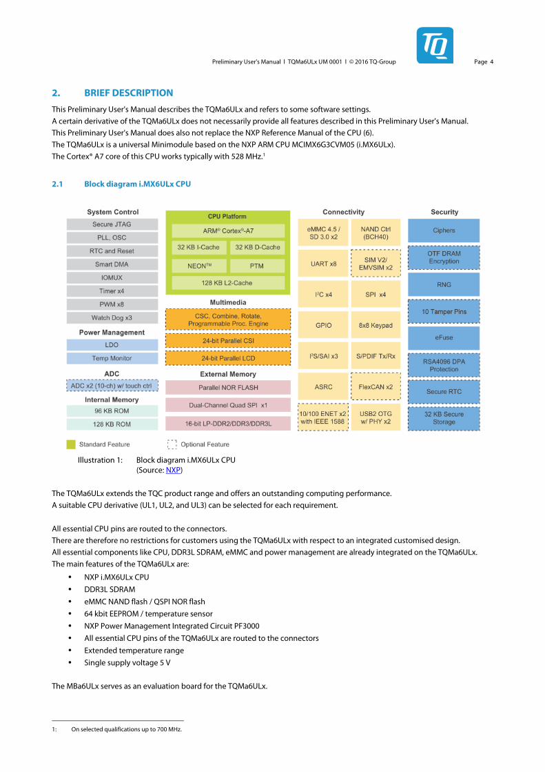
2.1 Block diagram i.MX6ULx CPU
Illustration 1: Block diagram i.MX6ULx CPU (Source: NXP)
The TQMa6ULx extends the TQC product range and offers an outstanding computing performance.
A suitable CPU derivative (UL1, UL2, and UL3) can be selected for each requirement.
All essential CPU pins are routed to the connectors.
There are therefore no restrictions for customers using the TQMa6ULx with respect to an integrated customised design.
All essential components like CPU, DDR3L SDRAM, eMMC and power management are already integrated on the TQMa6ULx.
The main features of the TQMa6ULx are:
• NXP i.MX6ULx CPU
• DDR3L SDRAM
• eMMC NAND flash / QSPI NOR flash
• 64 kbit EEPROM / temperature sensor
• NXP Power Management Integrated Circuit PF3000
• All essential CPU pins of the TQMa6ULx are routed to the connectors
• Extended temperature range
• Single supply voltage 5 V
The MBa6ULx serves as an evaluation board for the TQMa6ULx.
1: On selected qualifications up to 700 MHz.
Preliminary User's Manual l TQMa6ULx UM 0001 l © 2016 TQ-Group Page 5
2.2 Key functions and characteristics
The following components are implemented on the TQMa6ULx:
• i.MX6ULx CPU
• DDR3L SDRAM
• eMMC NAND flash
• QSPI NOR flash
• EEPROM
• Temperature sensor
• Supervisor with Reset structure
• Power supply by PMIC with Power Sequencing
• 2 Connectors (200 pins)
The following interfaces are provided at the connectors of the TQMa6ULx2:
• 2 × Ethernet 10/100 RMII
• 2 × I2C (1 × for the devices on the TQMa6ULx)
• 1 × JTAG
• 1 × Parallel LCD RGB 24-bit interface
• 2 × CAN
• 2 × I2C
• 1 × SPI
• 2 × USB 2.0 OTG
• 11 × GPIO
• 3 × UART (with handshake)
• 1 × SD 4-bit (SDIO / MMC / SD card)
• 10 × Tamper
• 1 × differential clock (CCM)
• 1 × QSPI (for second SPI NOR flash; SS1)
By adapting the pin configuration, further interfaces of the i.MX6ULx are also available as an alternative to the mentioned factory configuration. These are amongst other:
• Camera Sensor-Interfaces 8-bit (CSI – CMOS Sensor Interface)
• Synchronous Audio Interface (SAI – e.g., I2S)
• PWM
• ADC
• Enhanced Periodic Interrupt Timer
• General Purpose Media Interface
• General Purpose Timer
• Keypad Port
• More audio interfaces
• One more I2C interface
• More SPI interfaces
• More UARTs
2: Number of interfaces depends on the i.MX6ULx derivative.
Preliminary User's Manual l TQMa6ULx UM 0001 l © 2016 TQ-Group Page 6
3. ELECTRONICS
The information in this Preliminary User's Manual is only valid in connection with the boot loader adapted for the TQMa6ULx, which is preinstalled on every TQMa6ULx (see also section 5) and the BSP provided by TQ-Systems GmbH.
Illustration 2: Block diagram TQMa6ULx (simplified)
3.1 Interfaces to other systems and devices
3.1.1 Pin multiplexing
When using the processor signals, the multiple pin configurations by different processor-internal function units must be taken note of. The pin assignment listed in Table 2 and Table 3 refer to the corresponding standard TQ-BSP of TQ-Systems GmbH in combination with the Starterkit MBa6ULx.
NXP provides a tool showing the multiplexing and simplifies the selection and configuration (i.MX Pins Tool – NXP Tool).
The electrical and pin characteristics are to be taken from the Data Sheets of the CPU (1), (2), (5), the Reference Manual of the CPU (6), and the Data Sheet of the PMIC (7).
Attention: Destruction or malfunction
Depending on the configuration, many of the CPU pins can provide several different functions.
Please take note of the information concerning the configuration of these pins in the i.MX6ULx Reference Manual (6), before integration or start-up of your carrier board / Starterkit.
Improper programming by operating software can cause malfunctions, deterioration or destruction of the TQMa6ULx.
Preliminary User's Manual l TQMa6ULx UM 0001 l © 2016 TQ-Group Page 7
3.1.1.1 Connector X1
Table 2: Pinout connector X1
CPU ball I/O Level Group Signal Pin Signal Group Level I/O CPU ball
– P 5 V Power VCC5V 1 2 VCC5V Power 5 V P –
– P 5 V Power VCC5V 3 4 VCC5V Power 5 V P –
– P 5 V Power VCC5V 5 6 VCC5V Power 5 V P –
– P 0 V Ground DGND 7 8 DGND Ground 0 V P –
– P 0 V Ground DGND 9 10 LICELL3 Power 3.3 V P –
– P 1.8 V Power VCC1V8_OUT 11 12 DGND Ground 0 V P –
– P 0 V Ground DGND 13 14 VCC3V3_V33_OUT Power 3.3 V P –
– P 3.0 V Power VSNVS_REF_OUT 15 16 DGND Ground 0 V P –
– P 3.3 V Power VCC3V3_REF_OUT 17 18 VCC2V5_OUT Power 2.5 V P –
– P 0 V Ground DGND 19 20 DGND Ground 0 V P –
– P 0.675 V Power VCCDDR_OUT 21 22 VCCCORE_OUT Power 1.4 V P –
– P 0 V Ground DGND 23 24 DGND Ground 0 V P –
F4 P 1.8 / 3.3 V4 Power NVCC_CSI 25 26 NVCC_ENET Power 2.5 / 3.3 V5 P F13
– P 0 V Ground DGND 27 28 DGND Ground 0 V P –
P17 O 2.5 V CCM CCM_CLK1_P 29 30 DGND Ground 0 V P –
P16 O 2.5 V CCM CCM_CLK1_N 31 32 DGND Ground 0 V P –
– P 0 V Ground DGND 33 34 DGND Ground 0 V P –
R8 I 3.3 V Config MX6ULx_ONOFF 35 36 USB_OTG2_OC USB 3.3 V I L17
T9 I 3.3 V Config PMIC_PWRON 37 38 USB_OTG2_PWR USB 3.3 V O L14
– P 0 V Ground DGND 39 40 DGND Ground 0 V P –
U16 O Open-Drain USB USB_OTG1_CHD# 41 42 USB_OTG2_VBUS Power 5 V P U12
– P 0 V Ground DGND 43 44 USB_OTG2_ID USB 3.3 V I M17
T12 P 5 V Power USB_OTG1_VBUS 45 46 DGND Ground 0 V P –
K13 I 3.3 V USB USB_OTG1_ID 47 48 USB_OTG2_DN USB 3 V I/O T13
L15 I 3.3 V USB USB_OTG1_OC 49 50 USB_OTG2_DP USB 3 V I/O U13
M16 O 3.3 V USB USB_OTG1_PWR 51 52 DGND Ground 0 V P –
– P 0 V Ground DGND 53 54 UART3_RX_DATA UART 3.3 V I H16
T15 I/O 3 V USB USB_OTG1_DN 55 56 UART3_TX_DATA UART 3.3 V O H17
U15 I/O 3 V USB USB_OTG1_DP 57 58 DGND Ground 0 V P –
– P 0 V Ground DGND 59 60 BOOT_MODE0 Boot 3.0 V6 I T10
N8 I 3.3 V SNVS SNVS_TAMPER5 61 62 BOOT_MODE1 Boot 3.0 V6 I U10
N11 I 3.3 V SNVS SNVS_TAMPER6 63 64 DGND Ground 0 V P –
N10 I 3.3 V SNVS SNVS_TAMPER7 65 66 SNVS_TAMPER0 SNVS 3.3 V I R10
N9 I 3.3 V SNVS SNVS_TAMPER8 67 68 SNVS_TAMPER1 SNVS 3.3 V I R9
R6 I 3.3 V SNVS SNVS_TAMPER9 69 70 SNVS_TAMPER2 SNVS 3.3 V I P11
– P 0 V Ground DGND 71 72 SNVS_TAMPER3 SNVS 3.3 V I P10
M14 I 3.3 V JTAG JTAG_TCK 73 74 SNVS_TAMPER4 SNVS 3.3 V I P9
P14 I 3.3 V JTAG JTAG_TMS 75 76 DGND Ground 0 V P –
N16 I 3.3 V JTAG JTAG_TDI 77 78 JTAG_TDO JTAG 3.3 V O N15
– P 0 V Ground DGND 79 80 JTAG_TRST# JTAG 3.3 V I N14
M15 I/O 3.3 V GPIO GPIO1_IO09 81 82 JTAG_MOD JTAG 3.3 V I P15
K15 I/O 3.3 V GPIO GPIO1_IO18 83 84 DGND Ground 0 V P –
J14 I/O 3.3 V GPIO GPIO1_IO19 85 86 UART1_RX_DATA UART 3.3 V I K16
J16 3.3 V I2C I2C4_SDA 87 88 UART1_TX_DATA UART 3.3 V O K14
J17 3.3 V I2C I2C4_SCL 89 90 DGND Ground 0 V P –
– P 0 V Ground DGND 91 92 CAN2_RX CAN 3.3 V I H14
– I – RFU RFU1 93 94 CAN2_TX CAN 3.3 V O J15
P8 I 3.3 V Config RESET_IN# 95 96 CAN1_RX CAN 3.3 V I G14
– O 3.3 V Config RESET_OUT# 97 98 CAN1_TX CAN 3.3 V O H15
– P 0 V Ground DGND 99 100 DGND Ground 0 V P –
3: LICELL can be left open, if RTC backup or other functions of the SNVS domain are not required (see NXP documentation). 4: 1.8 V, if NVCC_CSI is connected to VCC1V8_OUT. 3.3 V, if NVCC_CSI is connected to VCC3V3_V33_OUT. 5: 2.5 V, if NVCC_ENET is connected to VCC2V5_OUT. 3.3 V, if NVCC_ENET is connected to VCC3V3_REF_OUT. 6: Use VSNVS_REF_OUT as reference voltage for BOOT-CFG resistors.
Preliminary User's Manual l TQMa6ULx UM 0001 l © 2016 TQ-Group Page 8
3.1.1.2 Connector X2
Table 3: Pinout connector X2
CPU ball I/O Level Group Signal Pin Signal Group Level I/O CPU ball
– P 0 V Ground DGND 1 2 DGND Ground 0 V P –
G16 O 3.3 V SPI SPI2_SS0# 3 4 SPI2_MISO SPI 3.3 V I G13
G17 O 3.3 V SPI SPI2_SCLK 5 6 SPI2_MOSI SPI 3.3 V O F17
F15 O 2.5 / 3.3 V7 ENET ENET1_TX_EN 7 8 DGND Ground 0 V P –
F14 O 2.5 / 3.3 V7 ENET ENET1_TX_CLK 9 10 ENET_MGMT_MDC ENET 2.5 / 3.3 V7 O L16
– P 0 V Ground DGND 11 12 ENET_MGMT_MDIO ENET 2.5 / 3.3 V7 I/O K17
E15 O 2.5 / 3.3 V7 ENET ENET1_TDATA0 13 14 ENET2_TX_CLK ENET 2.5 / 3.3 V7 O D17
E14 O 2.5 / 3.3 V7 ENET ENET1_TDATA1 15 16 DGND Ground 0 V P –
F16 I 2.5 / 3.3 V7 ENET ENET1_RDATA0 17 18 ENET2_RX_ER ENET 2.5 / 3.3 V7 I D16
E17 I 2.5 / 3.3 V7 ENET ENET1_RDATA1 19 20 ENET2_RDATA1 ENET 2.5 / 3.3 V7 I C16
E16 I 2.5 / 3.3 V7 ENET ENET1_RX_EN 21 22 ENET2_RDATA0 ENET 2.5 / 3.3 V7 I C17
D15 I 2.5 / 3.3 V7 ENET ENET1_RX_ER 23 24 ENET2_RX_EN ENET 2.5 / 3.3 V7 I B17
– P 0 V Ground DGND 25 26 ENET2_TX_EN ENET 2.5 / 3.3 V7 O B15
B16 I/O 3.3 V8 LCD LCD_DATA23 27 28 ENET2_TDATA0 ENET 2.5 / 3.3 V7 O A15
A14 I/O 3.3 V8 LCD LCD_DATA22 29 30 ENET2_TDATA1 ENET 2.5 / 3.3 V7 O A16
B14 I/O 3.3 V8 LCD LCD_DATA21 31 32 DGND Ground 0 V P –
C14 I/O 3.3 V8 LCD LCD_DATA20 33 34 LCD_DATA15 LCD 3.3 V8 I/O D13
– P 0 V Ground DGND 35 36 LCD_DATA14 LCD 3.3 V8 I/O A12
D14 I/O 3.3 V8 LCD LCD_DATA19 37 38 LCD_DATA13 LCD 3.3 V8 I/O B12
A13 I/O 3.3 V8 LCD LCD_DATA18 39 40 LCD_DATA12 LCD 3.3 V8 I/O C12
B13 I/O 3.3 V8 LCD LCD_DATA17 41 42 DGND Ground 0 V P –
C13 I/O 3.3 V8 LCD LCD_DATA16 43 44 LCD_DATA11 LCD 3.3 V8 I/O D12
– P 0 V Ground DGND 45 46 LCD_DATA10 LCD 3.3 V8 I/O E12
D11 I/O 3.3 V8 LCD LCD_DATA07 47 48 LCD_DATA09 LCD 3.3 V8 I/O A11
A10 I/O 3.3 V8 LCD LCD_DATA06 49 50 LCD_DATA08 LCD 3.3 V8 I/O B11
B10 I/O 3.3 V8 LCD LCD_DATA05 51 52 DGND Ground 0 V P –
C10 I/O 3.3 V8 LCD LCD_DATA04 53 54 LCD_CLK LCD 3.3 V8 O A8
– P 0 V Ground DGND 55 56 DGND Ground 0 V P –
D10 I/O 3.3 V8 LCD LCD_DATA03 57 58 LCD_ENABLE LCD 3.3 V8 O B8
E10 I/O 3.3 V8 LCD LCD_DATA02 59 60 LCD_RESET LCD 3.3 V8 O E9
A9 I/O 3.3 V8 LCD LCD_DATA01 61 62 LCD_HSYNC LCD 3.3 V8 O D9
B9 I/O 3.3 V8 LCD LCD_DATA00 63 64 LCD_VSYNC LCD 3.3 V8 I/O C9
– P 0 V Ground DGND 65 66 QSPI_A_DATA0 QSPI 3.3 V I/O A3
B3 I/O 3.3 V SD SD1_DATA0 67 68 QSPI_A_DATA1 QSPI 3.3 V I/O C5
B2 I/O 3.3 V SD SD1_DATA1 69 70 QSPI_A_DATA2 QSPI 3.3 V I/O B5
B1 I/O 3.3 V SD SD1_DATA2 71 72 QSPI_A_DATA3 QSPI 3.3 V I/O A4
A2 I/O 3.3 V SD SD1_DATA3 73 74 QSPI_A_SS1# QSPI 3.3 V O A5
C2 I/O 3.3 V SD SD1_CMD 75 76 DGND Ground 0 V P –
– P 0 V Ground DGND 77 78 QSPI_A_SCK QSPI 3.3 V O D5
C1 O 3.3 V SD SD1_CLK 79 80 DGND Ground 0 V P –
– P 0 V Ground DGND 81 82 RFU2 RFU – I –
E4 I/O 3.3 V9 GPIO GPIO4_IO21 83 84 DGND Ground 0 V P –
E3 I/O 1.8 / 3.3 V9 GPIO GPIO4_IO22 85 86 GPIO4_IO25 GPIO 1.8 / 3.3 V9 I/O D4
– P 0 V Ground DGND 87 88 GPIO4_IO26 GPIO 1.8 / 3.3 V9 I/O D3
E2 I/O 1.8 / 3.3 V9 GPIO GPIO4_IO23 89 90 GPIO4_IO27 GPIO 1.8 / 3.3 V9 I/O D2
E1 I/O 1.8 / 3.3 V9 GPIO GPIO4_IO24 91 92 GPIO4_IO28 GPIO 1.8 / 3.3 V9 I/O D1
– I – RFU RFU3 93 94 DGND Ground 0 V P –
F3 O 3.3 V I2C I2C2_SCL 95 96 UART6_RX_DATA UART 3.3 V I E5
F2 I/O 3.3 V I2C I2C2_SDA 97 98 UART6_TX_DATA UART 3.3 V O F5
– P 0 V Ground DGND 99 100 DGND Ground 0 V P –
7: 2.5 V, if NVCC_ENET is connected to VCC2V5_OUT. 3.3 V, if NVCC_ENET is connected to VCC3V3_REF_OUT. 8: Use VCC3V3_REF_OUT as reference voltage for BOOT-CFG resistors. 9: 1.8 V, if NVCC_CSI is connected to VCC1V8_OUT. 3.3 V, if NVCC_CSI is connected to VCC3V3_V33_OUT.
Preliminary User's Manual l TQMa6ULx UM 0001 l © 2016 TQ-Group Page 9
3.2 System components
3.2.1 i.MX6ULx CPU
3.2.1.1 CPU derivatives
Depending on the derivative of the TQMa6ULx one of the following derivatives of the CPU is assembled:
Table 4: CPU derivatives
Description CPU clock Temperature Supported by TQ-BSP
MCIMX6G1CVM05AA 528 MHz –40 °C to +105 °C Yes
MCIMX6G2CVM05AA 528 MHz –40 °C to +105 °C Yes
MCIMX6G3CVM05AA 528 MHz –40 °C to +105 °C Yes
3.2.1.2 CPU errata
Attention: Malfunction
Please take note of the current errata of the i.MX6ULx CPU (2).
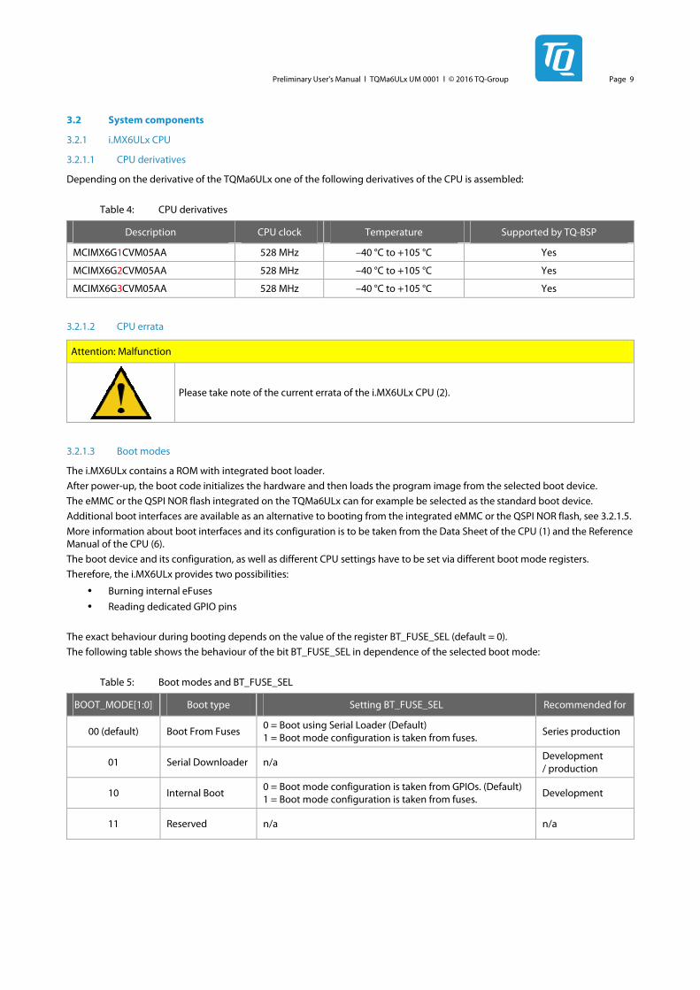
3.2.1.3 Boot modes
The i.MX6ULx contains a ROM with integrated boot loader.
After power-up, the boot code initializes the hardware and then loads the program image from the selected boot device.
The eMMC or the QSPI NOR flash integrated on the TQMa6ULx can for example be selected as the standard boot device.
Additional boot interfaces are available as an alternative to booting from the integrated eMMC or the QSPI NOR flash, see 3.2.1.5.
More information about boot interfaces and its configuration is to be taken from the Data Sheet of the CPU (1) and the Reference Manual of the CPU (6).
The boot device and its configuration, as well as different CPU settings have to be set via different boot mode registers.
Therefore, the i.MX6ULx provides two possibilities:
• Burning internal eFuses
• Reading dedicated GPIO pins
The exact behaviour during booting depends on the value of the register BT_FUSE_SEL (default = 0).
The following table shows the behaviour of the bit BT_FUSE_SEL in dependence of the selected boot mode:
Table 5: Boot modes and BT_FUSE_SEL
BOOT_MODE[1:0] Boot type Setting BT_FUSE_SEL Recommended for
00 (default) Boot From Fuses 0 = Boot using Serial Loader (Default) 1 = Boot mode configuration is taken from fuses.
Series production
01 Serial Downloader n/a Development / production
10 Internal Boot 0 = Boot mode configuration is taken from GPIOs. (Default) 1 = Boot mode configuration is taken from fuses.
Development
11 Reserved n/a n/a
Preliminary User's Manual l TQMa6ULx UM 0001 l © 2016 TQ-Group Page 10
3.2.1.4 Boot configuration
Note: Boot configuration
QSPI NOR flash is set as boot device when the TQMa6ULx is delivered.
Some general settings are done with some eFuses independent from the boot device:
Table 6: General boot settings
Signal / eFuse Pin name Ball Setting Default TQMa6ULx10
BOOT_CFG1[7:0] LCD_DATA[7:0] – Boot configuration 1:
Specific to selected boot mode – 000 1000
BOOT_CFG2[7:3]
BOOT_CFG2[1:0]
LCD_DATA[15:11]
LCD_DATA[9:8] –
Boot configuration 2:
Specific to selected boot mode – –
BOOT_CFG2[2] LCD_DATA10 E12
Boot frequencies (ARM / DDR):
0 = 500 / 400 MHz
1 = 250 / 200 MHz
0 –
BOOT_CFG3[7:0] – – Reserved – –
BOOT_CFG4[6:0] – – Boot configuration 4:
Specific to selected boot mode – –
BOOT_CFG4[7] LCD_DATA23 B16
Debug loop:
0 = Loop disabled
1 = Loop enabled
0 –
3.2.1.5 Boot interfaces
In the next sections, the configuration of the following boot devices is described:
• eMMC
• QSPI NOR flash
• SD card
10: Recommended settings.

Preliminary User's Manual l TQMa6ULx UM 0001 l © 2016 TQ-Group Page 11
3.2.1.6 Boot device eMMC
Table 7: Boot configuration eMMC at USDHC2
Signal / eFuse Pin name Ball Setting Default TQMa6ULx11
BOOT_CFG1[7] LCD_DATA07 D11 0 0
BOOT_CFG1[6] LCD_DATA06 A10
Boot Device Selection:
01 = Boot from USDHC Interface 0 1
BOOT_CFG1[5] LCD_DATA05 B10 SD/MMC Selection:
0 = SD/eSD/SDXC 1 = MMC/eMMC
0 1
BOOT_CFG1[4] LCD_DATA04 C10 Fast Boot:
0 = Regular 1 = Fast boot
0 0
BOOT_CFG1[3] LCD_DATA03 D10 0 0
BOOT_CFG1[2] LCD_DATA02 E10
MMC Speed:
0x = Normal Speed Mode 1x = High Speed Mode 0 0
BOOT_CFG1[1] LCD_DATA01 A9 eMMC Reset Enable:
0 = No action 1 = eMMC reset enabled (SD_RST pad)
0 0
BOOT_CFG1[0] LCD_DATA00 B9 SD Loopback Clock Source Selection:
0 = through SD pad 1 = direct
0 0
BOOT_CFG2[7] LCD_DATA15 D13 0 0
BOOT_CFG2[6] LCD_DATA14 A12 0 0
BOOT_CFG2[5] LCD_DATA13 B12
eMMC Bus Width:
000 = 1-bit 001 = 4-bit 010 = 8-bit 101 = 4-bit DDR (MMC 4.4) 110 = 8-bit DDR (MMC 4.4)
0 0
BOOT_CFG2[4] LCD_DATA12 C12 0 0
BOOT_CFG2[3] LCD_DATA11 D12
Port Select:
00 = USDHC1 01 = USDHC2 0 1
BOOT_CFG2[2] LCD_DATA10 E12 Boot Frequencies (ARM / DDR):
0 = 500 / 400 MHz 1 = 250 / 200 MHz
0 0
BOOT_CFG2[1] LCD_DATA09 A11 USDHC2 Voltage Selection:
0 = 3.3 V 1 = 1.8 V
0 0
In addition to the mode listed above the following eMMC modes are supported at port USDHC:
Table 8: USDHC2 mode eMMC
eMMC mode 1 bit 4 bit 8 bit 8 bit DDR
Normal speed × × × ×
High speed × × × ×
11: Recommended settings.
Preliminary User's Manual l TQMa6ULx UM 0001 l © 2016 TQ-Group Page 12
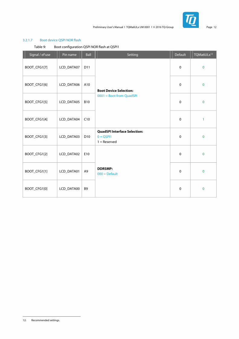
3.2.1.7 Boot device QSPI NOR flash
Table 9: Boot configuration QSPI NOR flash at QSPI1
Signal / eFuse Pin name Ball Setting Default TQMa6ULx12
BOOT_CFG1[7] LCD_DATA07 D11 0 0
BOOT_CFG1[6] LCD_DATA06 A10 0 0
BOOT_CFG1[5] LCD_DATA05 B10 0 0
BOOT_CFG1[4] LCD_DATA04 C10
Boot Device Selection:
0001 = Boot from QuadSPI
0 1
BOOT_CFG1[3] LCD_DATA03 D10
QuadSPI Interface Selection:
0 = QSPI1
1 = Reserved
0 0
BOOT_CFG1[2] LCD_DATA02 E10 0 0
BOOT_CFG1[1] LCD_DATA01 A9 0 0
BOOT_CFG1[0] LCD_DATA00 B9
DDRSMP:
000 = Default
0 0
12: Recommended settings.
Preliminary User's Manual l TQMa6ULx UM 0001 l © 2016 TQ-Group Page 13
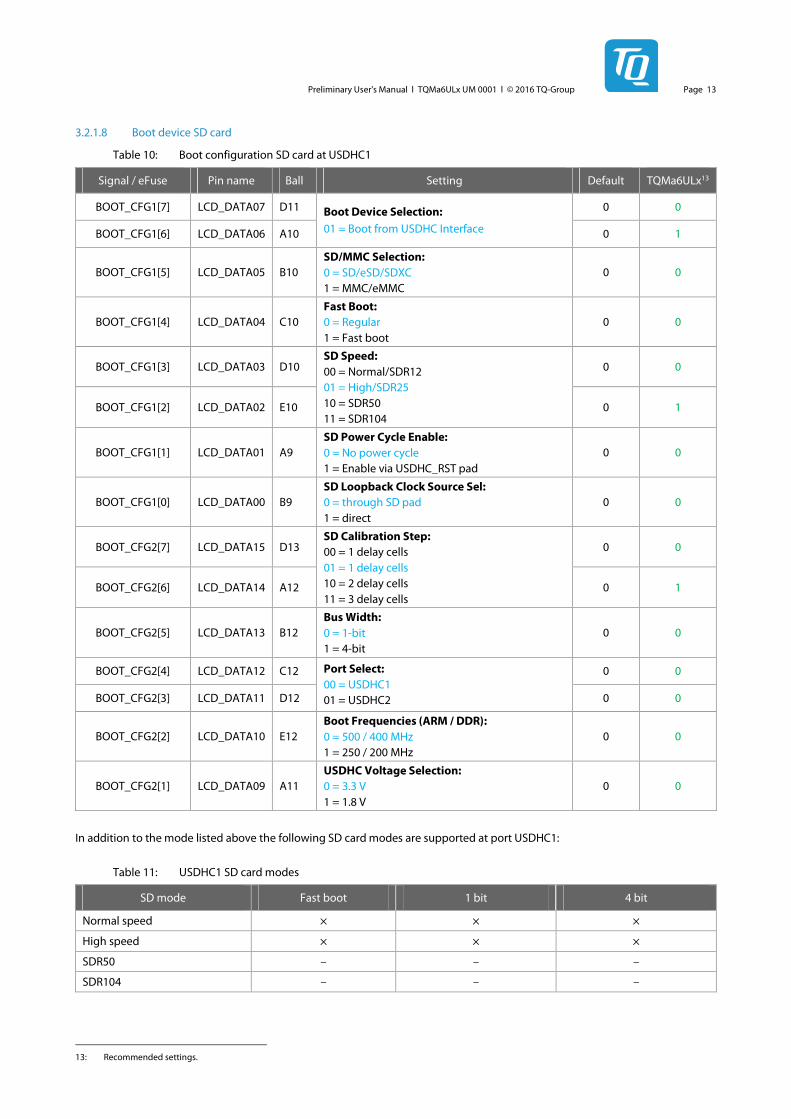
3.2.1.8 Boot device SD card
Table 10: Boot configuration SD card at USDHC1
Signal / eFuse Pin name Ball Setting Default TQMa6ULx13
BOOT_CFG1[7] LCD_DATA07 D11 0 0
BOOT_CFG1[6] LCD_DATA06 A10
Boot Device Selection:
01 = Boot from USDHC Interface 0 1
BOOT_CFG1[5] LCD_DATA05 B10 SD/MMC Selection:
0 = SD/eSD/SDXC 1 = MMC/eMMC
0 0
BOOT_CFG1[4] LCD_DATA04 C10 Fast Boot:
0 = Regular 1 = Fast boot
0 0
BOOT_CFG1[3] LCD_DATA03 D10 0 0
BOOT_CFG1[2] LCD_DATA02 E10
SD Speed:
00 = Normal/SDR12 01 = High/SDR25 10 = SDR50 11 = SDR104
0 1
BOOT_CFG1[1] LCD_DATA01 A9 SD Power Cycle Enable:
0 = No power cycle 1 = Enable via USDHC_RST pad
0 0
BOOT_CFG1[0] LCD_DATA00 B9 SD Loopback Clock Source Sel:
0 = through SD pad 1 = direct
0 0
BOOT_CFG2[7] LCD_DATA15 D13 0 0
BOOT_CFG2[6] LCD_DATA14 A12
SD Calibration Step:
00 = 1 delay cells 01 = 1 delay cells 10 = 2 delay cells 11 = 3 delay cells
0 1
BOOT_CFG2[5] LCD_DATA13 B12 Bus Width:
0 = 1-bit 1 = 4-bit
0 0
BOOT_CFG2[4] LCD_DATA12 C12 0 0
BOOT_CFG2[3] LCD_DATA11 D12
Port Select:
00 = USDHC1 01 = USDHC2 0 0
BOOT_CFG2[2] LCD_DATA10 E12 Boot Frequencies (ARM / DDR):
0 = 500 / 400 MHz 1 = 250 / 200 MHz
0 0
BOOT_CFG2[1] LCD_DATA09 A11 USDHC Voltage Selection:
0 = 3.3 V 1 = 1.8 V
0 0
In addition to the mode listed above the following SD card modes are supported at port USDHC1:
Table 11: USDHC1 SD card modes
SD mode Fast boot 1 bit 4 bit
Normal speed × × ×
High speed × × ×
SDR50 – – –
SDR104 – – –
13: Recommended settings.
Preliminary User's Manual l TQMa6ULx UM 0001 l © 2016 TQ-Group Page 14
3.2.2 Memory
3.2.2.1 DDR3L SDRAM
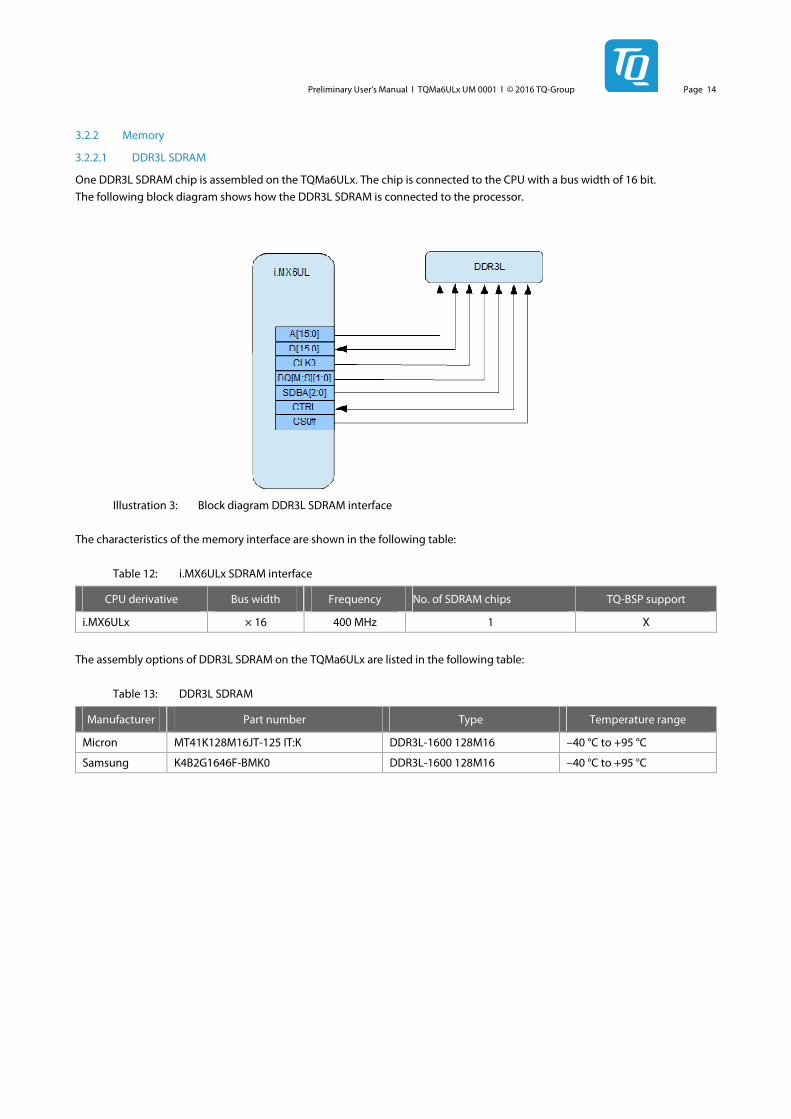
One DDR3L SDRAM chip is assembled on the TQMa6ULx. The chip is connected to the CPU with a bus width of 16 bit.
The following block diagram shows how the DDR3L SDRAM is connected to the processor.
Illustration 3: Block diagram DDR3L SDRAM interface
The characteristics of the memory interface are shown in the following table:
Table 12: i.MX6ULx SDRAM interface
CPU derivative Bus width Frequency No. of SDRAM chips TQ-BSP support
i.MX6ULx × 16 400 MHz 1 X
The assembly options of DDR3L SDRAM on the TQMa6ULx are listed in the following table:
Table 13: DDR3L SDRAM
Manufacturer Part number Type Temperature range
Micron MT41K128M16JT-125 IT:K DDR3L-1600 128M16 –40 °C to +95 °C
Samsung K4B2G1646F-BMK0 DDR3L-1600 128M16 –40 °C to +95 °C
Preliminary User's Manual l TQMa6ULx UM 0001 l © 2016 TQ-Group Page 15
3.2.2.2 eMMC NAND flash
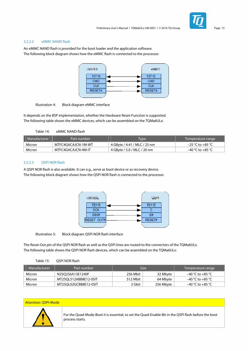
An eMMC NAND flash is provided for the boot loader and the application software.
The following block diagram shows how the eMMC flash is connected to the processor.
Illustration 4: Block diagram eMMC interface
It depends on the BSP implementation, whether the Hardware Reset-Function is supported.
The following table shows the eMMC devices, which can be assembled on the TQMa6ULx:
Table 14: eMMC NAND flash
Manufacturer Part number Type Temperature range
Micron MTFC4GACAJCN-1M-WT 4 GByte / 4.41 / MLC / 25 nm –25 °C to +85 °C
Micron MTFC4GACAJCN-4M-IT 4 GByte / 5.0 / MLC / 20 nm –40 °C to +85 °C
3.2.2.3 QSPI NOR flash
A QSPI NOR flash is also available. It can e.g., serve as boot device or as recovery device.
The following block diagram shows how the QSPI NOR flash is connected to the processor.
Illustration 5: Block diagram QSPI NOR flash interface
The Reset-Out pin of the QSPI NOR flash as well as the QSPI lines are routed to the connectors of the TQMa6ULx.
The following table shows the QSPI NOR flash devices, which can be assembled on the TQMa6ULx:
Table 15: QSPI NOR flash
Manufacturer Part number Size Temperature range
Micron N25Q256A13E1240F 256 Mbit 32 Mbyte –40 °C to +85 °C Micron MT25QL512ABB8E12-0SIT 512 Mbit 64 Mbyte –40 °C to +85 °C
Micron MT25QL02GCBB8E12-0SIT 2 Gbit 256 Mbyte –40 °C to +85 °C
Attention: QSPI-Mode
For the Quad-Mode-Boot it is essential, to set the Quad-Enable-Bit in the QSPI flash before the boot process starts.
Preliminary User's Manual l TQMa6ULx UM 0001 l © 2016 TQ-Group Page 16
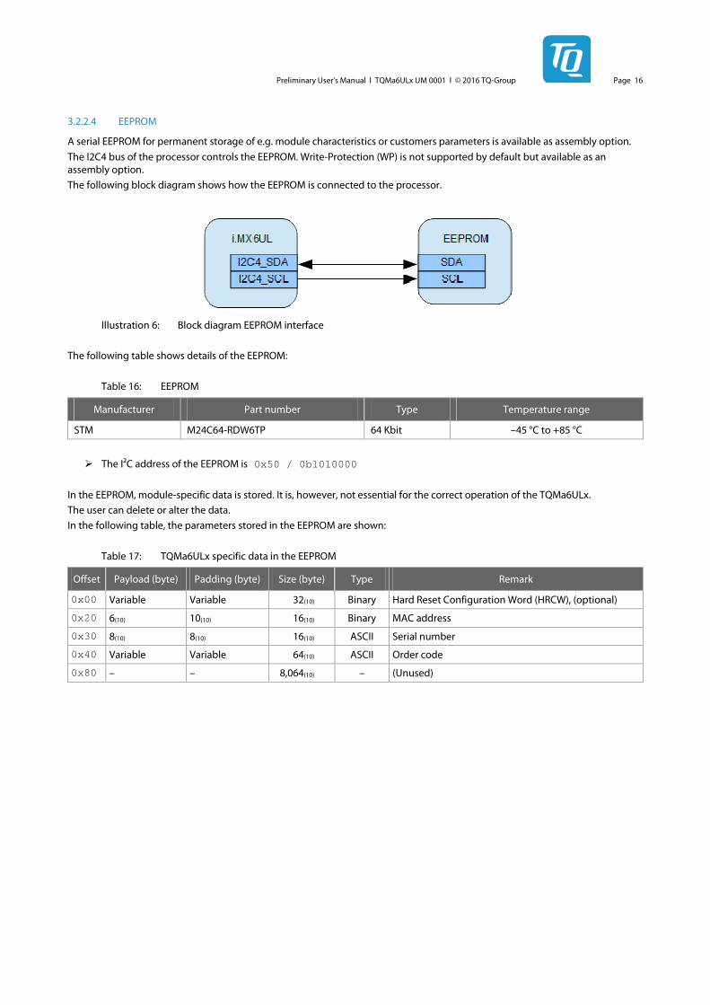
3.2.2.4 EEPROM
A serial EEPROM for permanent storage of e.g. module characteristics or customers parameters is available as assembly option.
The I2C4 bus of the processor controls the EEPROM. Write-Protection (WP) is not supported by default but available as an assembly option.
The following block diagram shows how the EEPROM is connected to the processor.
Illustration 6: Block diagram EEPROM interface
The following table shows details of the EEPROM:
Table 16: EEPROM
Manufacturer Part number Type Temperature range
STM M24C64-RDW6TP 64 Kbit –45 °C to +85 °C
The I2C address of the EEPROM is 0x50 / 0b1010000
In the EEPROM, module-specific data is stored. It is, however, not essential for the correct operation of the TQMa6ULx.
The user can delete or alter the data.
In the following table, the parameters stored in the EEPROM are shown:
Table 17: TQMa6ULx specific data in the EEPROM
Offset Payload (byte) Padding (byte) Size (byte) Type Remark
0x00 Variable Variable 32(10) Binary Hard Reset Configuration Word (HRCW), (optional)
0x20 6(10) 10(10) 16(10) Binary MAC address
0x30 8(10) 8(10) 16(10) ASCII Serial number
0x40 Variable Variable 64(10) ASCII Order code
0x80 – – 8,064(10) – (Unused)
Preliminary User's Manual l TQMa6ULx UM 0001 l © 2016 TQ-Group Page 17
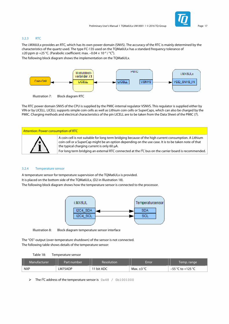
3.2.3 RTC
The i.MX6ULx provides an RTC, which has its own power domain (SNVS). The accuracy of the RTC is mainly determined by the characteristics of the quartz used. The type FC-135 used on the TQMa6ULx has a standard frequency tolerance of ±20 ppm @ +25 °C. (Parabolic coefficient: max. –0.04 × 10⁻⁶ / °C2).
The following block diagram shows the implementation on the TQMa6ULx.
Illustration 7: Block diagram RTC
The RTC power domain SNVS of the CPU is supplied by the PMIC-internal regulator VSNVS. This regulator is supplied either by VIN or by LICELL. LICELL supports simple coin cells as well as Lithium coin cells or SuperCaps, which can also be charged by the PMIC. Charging methods and electrical characteristics of the pin LICELL are to be taken from the Data Sheet of the PMIC (7).
Attention: Power consumption of RTC
A coin cell is not suitable for long term bridging because of the high current consumption. A Lithium coin cell or a SuperCap might be an option depending on the use case. It is to be taken note of that the typical charging current is only 60 µA.
For long term bridging an external RTC connected at the I2C bus on the carrier board is recommended.
3.2.4 Temperature sensor
A temperature sensor for temperature supervision of the TQMa6ULx is provided.
It is placed on the bottom side of the TQMa6ULx, (D2 in Illustration 18).
The following block diagram shows how the temperature sensor is connected to the processor.
Illustration 8: Block diagram temperature sensor interface
The “OS”-output (over-temperature shutdown) of the sensor is not connected.
The following table shows details of the temperature sensor:
Table 18: Temperature sensor
Manufacturer Part number Resolution Error Temp. range
NXP LM75ADP 11 bit ADC Max. ±3 °C –55 °C to +125 °C
The I2C address of the temperature sensor is 0x48 / 0b1001000
Preliminary User's Manual l TQMa6ULx UM 0001 l © 2016 TQ-Group Page 18
3.2.5 Interfaces
3.2.5.1 Overview
The TQMa6ULx provides interfaces with primary functions. They can all be used simultaneously independent of their configuration. Some of the primary functions are not available if a secondary function is used:
Table 19: Internal interfaces
Interface Number Function Section Remark
USDHC 1 Primary USDHC2 | eMMC, 8 data bits
MMDC 1 Primary DDR3L-SDRAM, 16 data bits
QSPI 1 Primary QSPI NOR flash, 4 data bits
Table 20: External interfaces
Interface Number Function Section Remark
CCM 2 Secondary Multiplexing has to be adapted
CSI 1 Secondary Multiplexing has to be adapted
ECSPI 1 Primary ECSPI2
ECSPI 2 Secondary ECPSI1 / ECSPI3 / ECSPI4 | Multiplexing has to be adapted
EIM 1 Secondary Multiplexing has to be adapted
ENET 2 Primary RMII (10/100 Mbit/s) / 1588 | Multiplexing has to be adapted
EPIT 2 Secondary Multiplexing has to be adapted
FLEXCAN 2 Primary FLEXCAN[2:1]
GPIO 11 Primary GPIO1 / GPIO4
GPT 2 Secondary GPT[2:1] | Multiplexing has to be adapted
I2C 2 Primary I2C2 / I2C4
I2C 2 Secondary I2C1 / I2C3 | Multiplexing has to be adapted
KPP 1 Secondary Multiplexing has to be adapted
LCDIF 1 Primary Graphics interface
MQS 1 Secondary Multiplexing has to be adapted
NAND 1 Secondary Multiplexing has to be adapted
PWM 8 Secondary PWM[8:1] | Multiplexing has to be adapted
SAI 3 Secondary SAI[3:1] | Multiplexing has to be adapted
SIM 2 Secondary Multiplexing has to be adapted
SJC 1 Primary JTAG
SNVS 1 Primary SNVS_TAMPER[9-0]
SRC 1 Secondary Depends on BOOT_MODE0 | BOOT_MODE1
SPDIF 1 Secondary Multiplexing has to be adapted
UART 3 Primary UART1 / UART3 / UART6
UART 5 Secondary UART2 / UART4 / UART[8:7] | Multiplexing has to be adapted
USB 2 Primary USB_OTG1 / USB_OTG2
USDHC 1 Primary SD card-Interface
WDOG 1 Secondary WDOG[3:1] | Multiplexing has to be adapted
XTALOSC 1 Primary CCM_CLK1_N / CCM_CLK1_P
In the following sections, only the external primary interfaces are described.
Preliminary User's Manual l TQMa6ULx UM 0001 l © 2016 TQ-Group Page 19
3.2.5.2 ECSPI - Enhanced Configurable SPI
The i.MX6ULx provides four ECSPI interfaces, which are all full-duplex and can be configured as Master/Slave.
Primarily ECSPI2 is available at the connectors of the TQMa6ULx.
The following table shows the signals used by the ECSPI2 interface:
Table 21: Signals ECSPI2
Signal name Direction Pin Remark
ECSPI2_MISO I
ECSPI2_MOSI O
ECSPI2_SCLK O
ECSPI2_SS0 O
3.2.5.3 ENET – Fast Ethernet
The i.MX6ULx provides a 10/100 MAC core, which supports MII (4 bit) and RMII (2 bit).
The RGMII signals are available as primary function at the connectors of the TQMa6ULx.
The following table shows the signals used by the RMII interface:
Table 22: Signals RMII
Signal name Power-Group Direction Pin Remark
ENET_MDC O
ENET_MDIO
NVCC_GPIO (3.3 V) I/O
ENET1_RDATA[1:0] I
ENET1_RX_EN I
ENET1_RX_ER I
ENET1_TDATA[1:0] O
ENET1_TX_CLK O
ENET1_TX_EN O
ENET2_RDATA[1:0] I
ENET2_RX_EN I
ENET2_RX_ER I
ENET2_TDATA[1:0] O
ENET2_TX_CLK O
ENET2_TX_EN
NVCC_ENET (2.5 V / 3.3 V)
O
Attention: NVCC_ENET
NVCC_ENET has to be connected externally!
The RMII interface of the i.MX6ULx works with an I/O voltage of 2.5 V or 3.3 V. In order to use the interface, additional signals of the signal group ENET are required. The accompanying power supply pin is routed to the connector to operate these signals on the same I/O voltage, if RMII is used.
By adapting the multiplexing, it is possible to use MII. Details are to be taken from the Reference Manual and the Data Sheet of the CPU (1), (6).
VCC3V3_REF_OUT or VCC3V3_V33_OUT can be used as I/O supply voltage for an RMII-PHY.
Preliminary User's Manual l TQMa6ULx UM 0001 l © 2016 TQ-Group Page 20
3.2.5.4 CAN – FLEXCAN
The i.MX6ULx provides two integrated CAN 2.0B controllers. Both signals pairs are available at the connectors of the TQMa6ULx.
The drivers required have to be implemented on the carrier board.
The following table shows the signals used by the CAN interface:
Table 23: Signals FLEXCAN
Signal name Direction Pin Remark
FLEXCAN1_RX I
FLEXCAN1_TX O
FLEXCAN2_RX I
FLEXCAN2_TX O
3.2.5.5 GPIO
Beside their interface function, most of the pins of the i.MX6ULx can also be configured as GPIO.
All these GPIOs can trigger an interrupt. Details are to be taken from the Reference Manual and the Data Sheet of the CPU (1), (6).
In addition, different pins are already marked as GPIO and are available on the connectors of the TQMa6ULx.
The following table shows the GPIO signals provided:
Table 24: Signals GPIO
Signal name Remark Direction Pin Remark
GPIO1_IO09 I/O
GPIO1_IO18 I/O
GPIO1_IO19 I/O
GPIO4_IO21 I/O
GPIO4_IO22 I/O
GPIO4_IO23 I/O
GPIO4_IO24 I/O
GPIO4_IO25 I/O
GPIO4_IO26 I/O
GPIO4_IO27 I/O
GPIO4_IO28
NVCC_CSI (1.8 V / 3.3 V)
I/O
Attention: NVCC_CSI
NVCC_CSI has to be connected externally!
The electrical characteristics of the GPIOs are to be taken from the Data Sheet of the CPU (1).
Preliminary User's Manual l TQMa6ULx UM 0001 l © 2016 TQ-Group Page 21
3.2.5.6 I2C
The i.MX6ULx provides four I2C interfaces.
I2C2 and I2C4 are routed to the connectors of the TQMa6ULx and are available as primary function.
The following table shows the signals used by the I2C interfaces:
Table 25: Signals I2C
Signal name Remark Direction Pin Remark
I2C2_SCL O
I2C2_SDA NVCC_CSI (1.8 V / 3.3 V)
I/O
I2C4_SCL O
I2C4_SDA PU 2.2 kΩ to 3.3 V on TQMa6ULx
I/O
Attention: NVCC_CSI
NVCC_CSI has to be connected externally!
The following table shows the I2C devices connected to the I2C1 bus on the TQMa6ULx:
Table 26: I2C address assignment
Component Address
EEPROM (M24C64) 0x50 / 0b1010000
Temperature sensor (LM75A) 0x48 / 0b1001000
PMIC (MC32PF3000A7EP) 0x08 / 0b0001000
If more devices are connected to the I2C buses on the carrier board, the maximum capacitive bus load according to the I2C standard has to be taken note of. If necessary, additional Pull-Ups at the bus should be provided on the carrier board.
3.2.5.7 eLCDIF – Enhanced LCD Interface
Die i.MX6ULx CPU provides a display controller, which supports displays of different size and performance. Information regarding types of displays and supported formats are to be taken from the Reference Manual of the CPU (6).
The LCD signals routed to the connectors of the TQMa6ULx as primary function.
The following table shows the signals used by the LCD interface:
Table 27: Signals LCD
Signal name Direction Pin Remark
LCDIF_CLK O
LCDIF_DATA[23:0] I/O
LCDIF_ENABLE O
LCDIF_HSYNC O
LCDIF_RESET O
LCDIF_VSYNC O
Preliminary User's Manual l TQMa6ULx UM 0001 l © 2016 TQ-Group Page 22
3.2.5.8 SJC – System JTAG Controller
The i.MX6ULx can operate in two different JTAG modes. The pin JTAG_MOD defines the mode.
The following table shows the existing modes as well as the mode set on the TQMa6ULx:
Table 28: JTAG modes
JTAG_MOD Default Name Remark
0 X Daisy Chain All For common SW debug (High speed and series production)
1 SJC only IEEE 1149.1 JTAG compliant mode
The following table shows the signals used by the JTAG interface:
Table 29: Signals JTAG
Signal name Direction Pin Remark
JTAG_TCK I i.MX6ULx internal PU 47 kΩ
JTAG_TMS I i.MX6ULx internal PU 47 kΩ
JTAG_TDI I i.MX6ULx internal PU 47 kΩ
JTAG_TDO O i.MX6ULx internal keeper
JTAG_TRST# I i.MX6ULx internal PU 47 kΩ
JTAG_MOD I PD 4.7 kΩ on TQMa6ULx + i.MX6ULx-internal PU 100 kΩ
3.2.5.9 TAMPER
The i.MX6ULx provides protection against unauthorised opening or manipulation of a device by tamper detection.
The TAMPER pins are available for this purpose at the connectors of the TQMa6ULx.
The following table shows the available signals:
Table 30: Signals TAMPER
Signal name Direction Pin Remark
SNVS_TAMPER[9:0] I
Details about the function of the TAMPER pins are to be taken from the Reference Manual of the CPU (6).
Preliminary User's Manual l TQMa6ULx UM 0001 l © 2016 TQ-Group Page 23
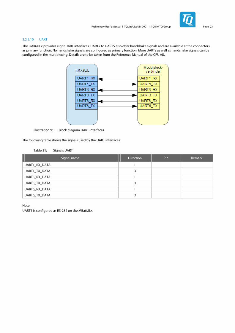
3.2.5.10 UART
The i.MX6ULx provides eight UART interfaces. UART2 to UART5 also offer handshake signals and are available at the connectors as primary function. No handshake signals are configured as primary function. More UARTs as well as handshake signals can be configured in the multiplexing. Details are to be taken from the Reference Manual of the CPU (6).
Illustration 9: Block diagram UART interfaces
The following table shows the signals used by the UART interfaces:
Table 31: Signals UART
Signal name Direction Pin Remark
UART1_RX_DATA I
UART1_TX_DATA O
UART3_RX_DATA I
UART3_TX_DATA O
UART6_RX_DATA I
UART6_TX_DATA O
Note:
UART1 is configured as RS-232 on the MBa6ULx.
Preliminary User's Manual l TQMa6ULx UM 0001 l © 2016 TQ-Group Page 24
3.2.5.11 USB
The i.MX6ULx provides two independent USB-OTG controllers with integrated High-Speed PHY.
Both USB-OTG controllers can operate in Host or in Device mode.
They are both available at the connectors of the TQMa6ULx as primary function.
The following table shows the signals used by the USB_OTG interfaces:
Table 32: Signals USB_OTG
Signal name Direction Pin Remark
USB_OTG1_ID I Device Mode: USB_OTG_ID signal is high, Host Mode : USB_OTG_ID signal is low
USB_OTG1_OC I
USB_OTG1_PWR O
USB_OTG1_VBUS P
USB_OTG1_DN I/O
USB_OTG1_DP I/O
USB_OTG2_ID I Device Mode: USB_OTG_ID signal is high, Host Mode : USB_OTG_ID signal is low
USB_OTG2_OC I
USB_OTG2_PWR O
USB_OTG2_VBUS P
USB_OTG2_DN I/O
USB_OTG2_DP I/O
3.2.5.12 USDHC – Ultra-Secured Digital Host Controller
The i.MX6ULx provides a USDHC controller, which is the interface between Host system and SD/SDIO/MMC cards.
To connect an MMC, SD, or SDIO card the USDHC1 port of the i.MX6ULx is routed to the connectors of the TQMa6ULx.
The following table shows the signals used by the USDHC interface:
Table 33: Signals USDHC1
Signal name Direction Pin Remark
USDHC1_CLK O
USDHC1_CMD I/O
USDHC1_DATA[3:0] I/O
3.2.5.13 XTAL – differential clock
The i.MX6ULx provides a differential clock output, which is routed to the connectors of the TQMa6ULx.
The following table shows details of the XTAL signals:
Table 34: Signals XTAL
Signal name Direction Pin Remark
CCM_CLK1_N O
CCM_CLK1_P O
Preliminary User's Manual l TQMa6ULx UM 0001 l © 2016 TQ-Group Page 25
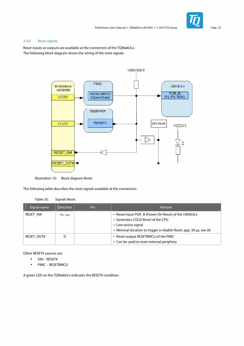
3.2.6 Reset signals
Reset inputs or outputs are available at the connectors of the TQMa6ULx.
The following block diagram shows the wiring of the reset signals.
Illustration 10: Block diagram Reset
The following table describes the reset signals available at the connectors:
Table 35: Signals Reset
Signal name Direction Pin Remark
RESET_IN# IPU_100k
• Reset input POR_B (Power-On Reset) of the i.MX6ULx
• Generates COLD-Reset of the CPU
• Low-active signal
• Minimal duration to trigger a reliable Reset: app. 30 µs, see (6)
RESET_OUT# O • Reset output RESETBMCU of the PMIC
• Can be used to reset external periphery
Other RESET# sources are:
• VIN – RESET#
• PMIC – RESETBMCU
A green LED on the TQMa6ULx indicates the RESET# condition.
Preliminary User's Manual l TQMa6ULx UM 0001 l © 2016 TQ-Group Page 26
3.2.7 Power supply
3.2.7.1 TQMa6ULx power supply
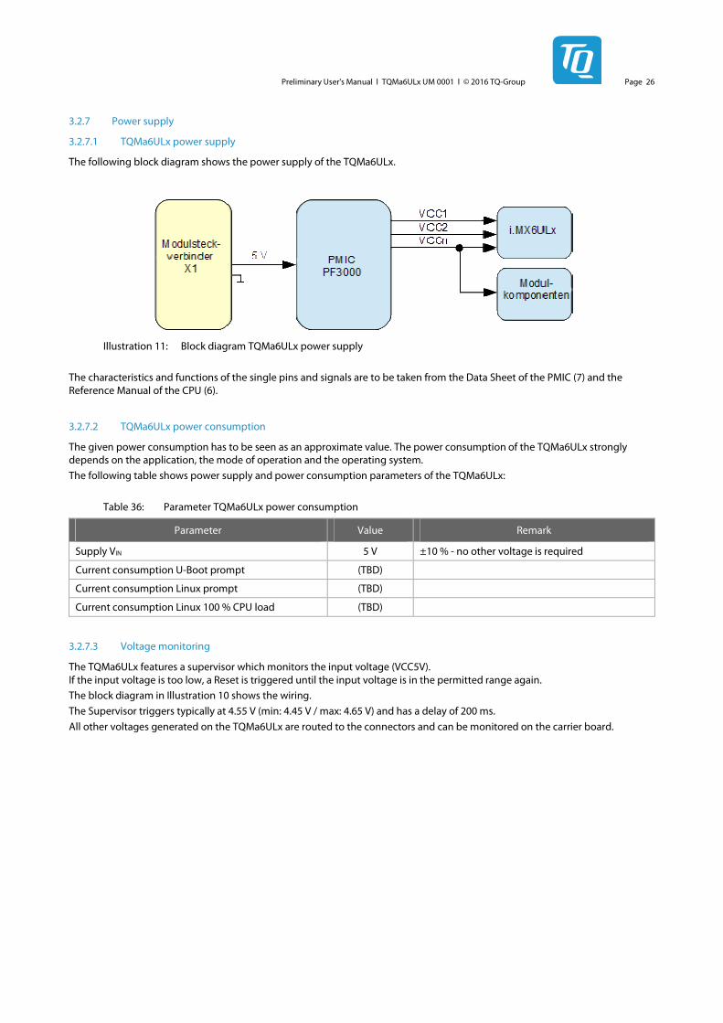
The following block diagram shows the power supply of the TQMa6ULx.
Illustration 11: Block diagram TQMa6ULx power supply
The characteristics and functions of the single pins and signals are to be taken from the Data Sheet of the PMIC (7) and the Reference Manual of the CPU (6).
3.2.7.2 TQMa6ULx power consumption
The given power consumption has to be seen as an approximate value. The power consumption of the TQMa6ULx strongly depends on the application, the mode of operation and the operating system.
The following table shows power supply and power consumption parameters of the TQMa6ULx:
Table 36: Parameter TQMa6ULx power consumption
Parameter Value Remark
Supply VIN 5 V ±10 % - no other voltage is required
Current consumption U-Boot prompt (TBD)
Current consumption Linux prompt (TBD)
Current consumption Linux 100 % CPU load (TBD)
3.2.7.3 Voltage monitoring
The TQMa6ULx features a supervisor which monitors the input voltage (VCC5V). If the input voltage is too low, a Reset is triggered until the input voltage is in the permitted range again.
The block diagram in Illustration 10 shows the wiring.
The Supervisor triggers typically at 4.55 V (min: 4.45 V / max: 4.65 V) and has a delay of 200 ms.
All other voltages generated on the TQMa6ULx are routed to the connectors and can be monitored on the carrier board.
Preliminary User's Manual l TQMa6ULx UM 0001 l © 2016 TQ-Group Page 27
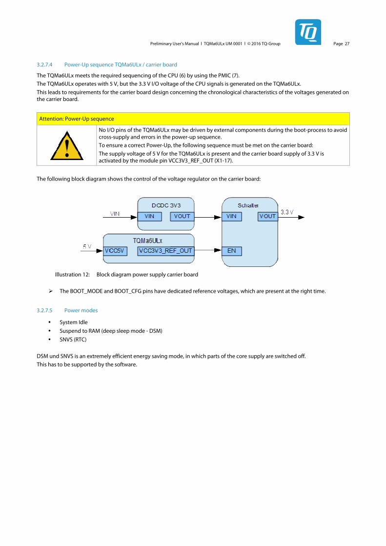
3.2.7.4 Power-Up sequence TQMa6ULx / carrier board
The TQMa6ULx meets the required sequencing of the CPU (6) by using the PMIC (7).
The TQMa6ULx operates with 5 V, but the 3.3 V I/O voltage of the CPU signals is generated on the TQMa6ULx.
This leads to requirements for the carrier board design concerning the chronological characteristics of the voltages generated on the carrier board.
Attention: Power-Up sequence
No I/O pins of the TQMa6ULx may be driven by external components during the boot-process to avoid cross-supply and errors in the power-up sequence.
To ensure a correct Power-Up, the following sequence must be met on the carrier board:
The supply voltage of 5 V for the TQMa6ULx is present and the carrier board supply of 3.3 V is activated by the module pin VCC3V3_REF_OUT (X1-17).
The following block diagram shows the control of the voltage regulator on the carrier board:
Illustration 12: Block diagram power supply carrier board
The BOOT_MODE and BOOT_CFG pins have dedicated reference voltages, which are present at the right time.
3.2.7.5 Power modes
• System Idle
• Suspend to RAM (deep sleep mode - DSM)
• SNVS (RTC)
DSM und SNVS is an extremely efficient energy saving mode, in which parts of the core supply are switched off.
This has to be supported by the software.
Preliminary User's Manual l TQMa6ULx UM 0001 l © 2016 TQ-Group Page 28
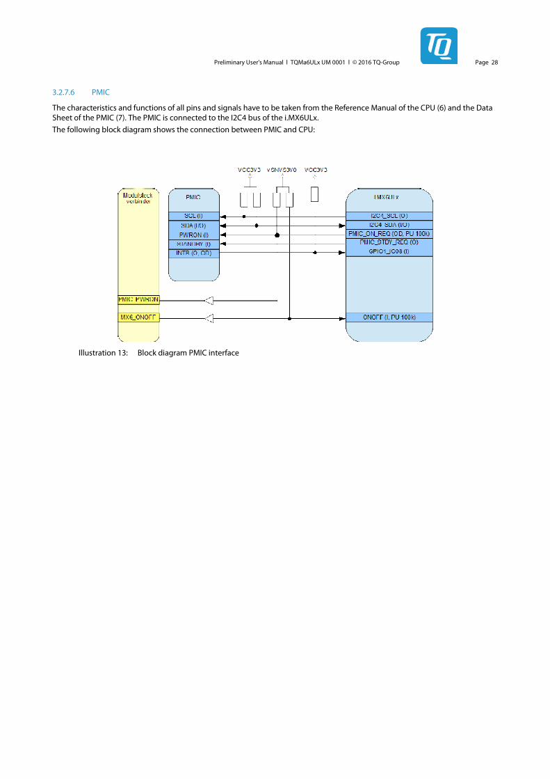
3.2.7.6 PMIC
The characteristics and functions of all pins and signals have to be taken from the Reference Manual of the CPU (6) and the Data Sheet of the PMIC (7). The PMIC is connected to the I2C4 bus of the i.MX6ULx.
The following block diagram shows the connection between PMIC and CPU:
Illustration 13: Block diagram PMIC interface
Preliminary User's Manual l TQMa6ULx UM 0001 l © 2016 TQ-Group Page 29
4. MECHANICS
4.1 Connectors
The TQMa6ULx is connected to the carrier board with 200 pins on three connectors.
The following table shows details of the plug connector:
Table 37: Plug connectors on the TQMa6ULx
Manufacturer Part number Remark
TE connectivity 100-pin: 5177985-4
0.8 mm pitch
Plating: Gold 0.2 µm
–40 °C to +125 °C
The TQMa6ULx is held in the plug connectors with a considerable retention force.
To avoid damaging the plug connectors of the TQMa6ULx as well as the plug connectors on the carrier board while removing the TQMa6ULx the use of an extraction tool is strongly recommended. See section 4.8 for further information.
The following table shows some suitable mating plug connectors for the carrier board.
Table 38: Suitable carrier board mating plug connectors
Manufacturer Part number Remark Stack height (X)
TE connectivity 100-pin: 5177986-4 On MBa6ULx 5 mm
TE connectivity 100-pin: 1-5177986-4 – 6 mm
TE connectivity 100-pin: 2-5177986-4 – 7 mm
TE connectivity 100-pin: 3-5177986-4 – 8 mm
The pins assignment listed in Table 2 and Table 3 refer to the corresponding standard BSP of TQ-Systems GmbH.
Information regarding I/Os in Table 2 and Table 3 refer to the CPU pins.
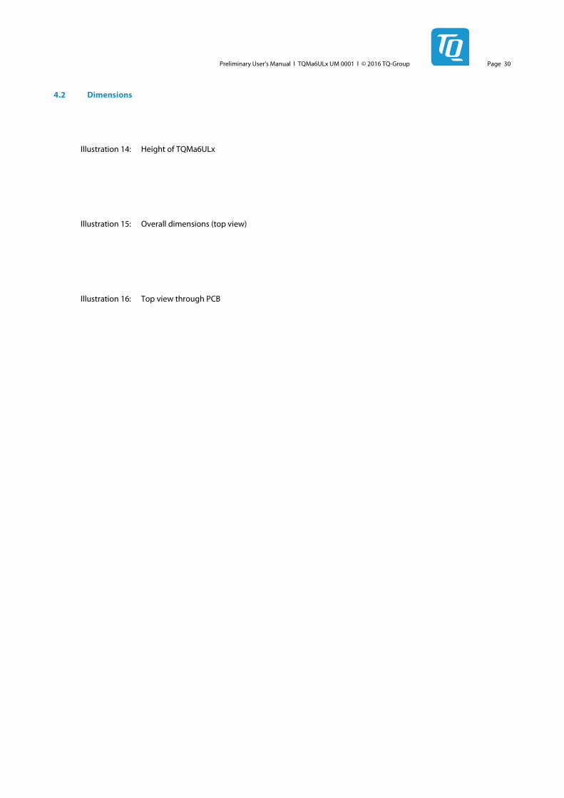
Preliminary User's Manual l TQMa6ULx UM 0001 l © 2016 TQ-Group Page 30
4.2 Dimensions
Illustration 14: Height of TQMa6ULx
Illustration 15: Overall dimensions (top view)
Illustration 16: Top view through PCB
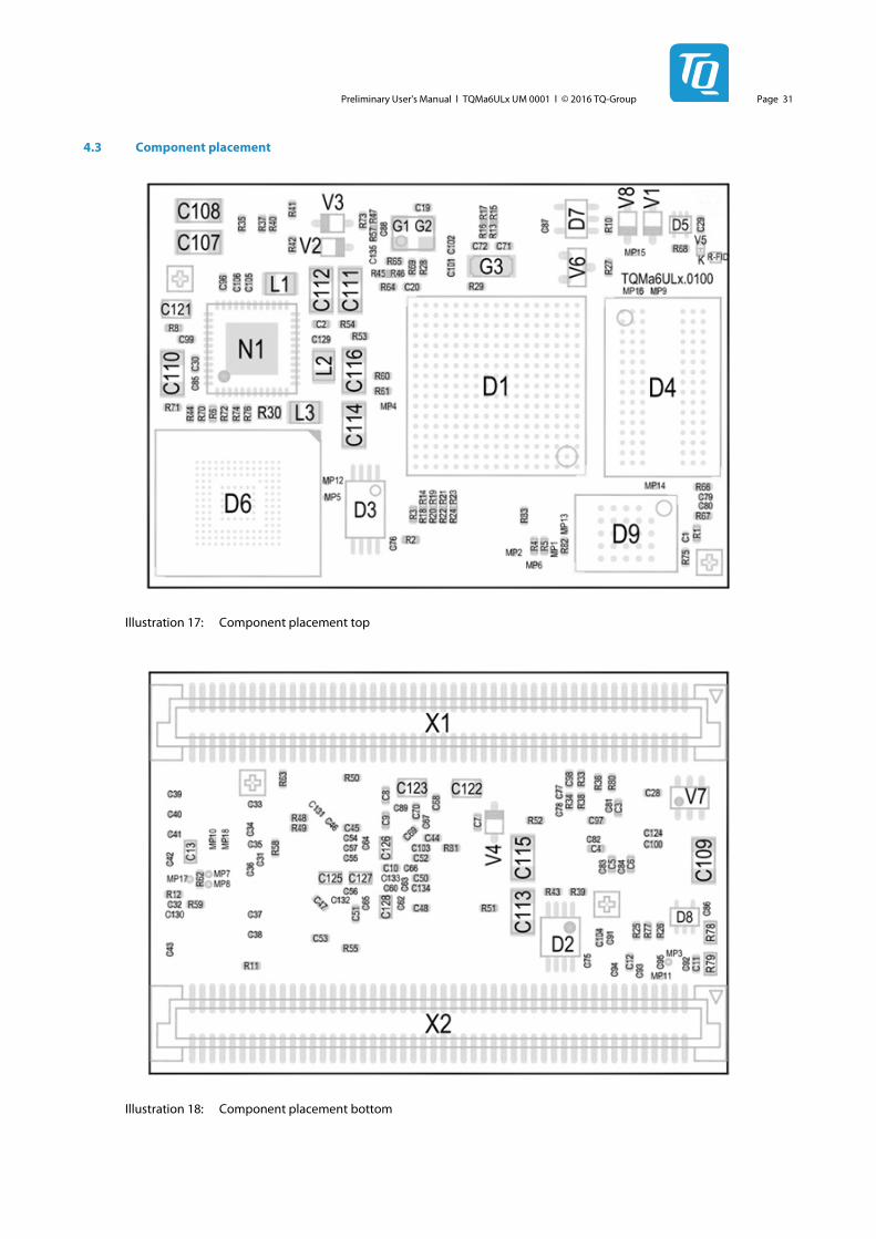
Preliminary User's Manual l TQMa6ULx UM 0001 l © 2016 TQ-Group Page 31
4.3 Component placement
Illustration 17: Component placement top
Illustration 18: Component placement bottom
Preliminary User's Manual l TQMa6ULx UM 0001 l © 2016 TQ-Group Page 32
4.4 Adaptation to the environment
The overall dimensions (length × width × height) of the TQMa6ULx are 46 × 32 × 7.4 mm3.
The maximum height of the TQMa6ULx above the carrier board is approximately 8.4 mm.
4.5 Protection against external effects
As an embedded module, the TQMa6ULx is not protected against dust, external impact and contact (IP00).
Adequate protection has to be guaranteed by the surrounding system.
4.6 Thermal management
To cool the TQMa6ULx, a theoretical maximum of approximately (TBD) have to be dissipated.
The power dissipation originates primarily in the CPU, the DDR3L SDRAM and the PMIC.
The power dissipation also depends on the software used and can vary according to the application.
See NXP documents (3) and (7) for further information.
Attention: Destruction or malfunction
The CPU belongs to a performance category in which a cooling system may be essential in certain applications. It is the responsibility of the customer to define a suitable cooling method depending on the specific mode of operation (e.g., dependence on clock frequency, stack height, airflow, and software).
4.7 Structural requirements
The TQMa6ULx is held in the mating plug connectors by the retention force of the pins (200). For high requirements with respect to vibration and shock firmness, an additional holder has to be provided in the final product to hold the TQMa6ULx in its position. For this purpose, TQ-Systems GmbH can provide a suitable solution. As no heavy and big components are assembled, no further requirements are given.
4.8 Notes of treatment
To avoid damage caused by mechanical stress, the TQMa6ULx may only be extracted from the carrier board by using the extraction tool MOZIA6ULx that can also be obtained separately.
Attention: Note with respect to the component placement of the carrier board
2.5 mm should be kept free on the carrier board, along the longitudinal edges on both sides of the TQMa6ULx for the extraction tool.
5. SOFTWARE
The TQMa6ULx is delivered with a preinstalled boot loader U-Boot and a TQ-BSP, which is configured for the MBa6ULx.
The boot loader U-Boot provides module-specific as well as board-specific settings, e.g.:
• CPU configuration
• PMIC configuration
• SDRAM configuration
• eMMC configuration
• Multiplexing
• Clocks
• Pin configuration
• Driver strengths
More information can be found in the Support Wiki for the TQMa6ULx.
Preliminary User's Manual l TQMa6ULx UM 0001 l © 2016 TQ-Group Page 33
6. SAFETY REQUIREMENTS AND PROTECTIVE REGULATIONS
6.1 EMC
The TQMa6ULx was developed according to the requirements of electromagnetic compatibility (EMC). Depending on the target system, anti-interference measures may still be necessary to guarantee the adherence to the limits for the overall system.
Following measures are recommended:
• Robust ground planes (adequate ground planes) on the printed circuit board
• A sufficient number of blocking capacitors in all supply voltages
• Fast or permanent clocked lines (e.g., clock) should be kept short; avoid interference of other signals by distance and / or shielding besides, take note of not only the frequency, but also the signal rise times
• Filtering of all signals, which can be connected externally (also "slow signals" and DC can radiate RF indirectly)
Since the TQMa6ULx operates on an application-specific carrier board, EMC or ESD tests only make sense for the whole device.
The TQMa6ULx it designed to pass the following test:
• EMC-Interference radiation: Measurement of the electrically radiated emission for standard, residential, commercial and light industrial environments in the range of 30 MHz to 6 GHz according to DIN EN 55022 A1:2007.
6.2 ESD
In order to avoid interspersion on the signal path from the input to the protection circuit in the system, the protection against electrostatic discharge should be arranged directly at the inputs of a system. As these measures always have to be implemented on the carrier board, no special preventive measures were planned on the TQMa6ULx.
Following measures are recommended for a carrier board:
• Generally applicable: Shielding of the inputs (shielding connected well to ground / housing on both ends)
• Supply voltages: Protection by suppressor diode(s)
• Slow signal lines: RC filtering, perhaps Zener diode(s)
• Fast signal lines: Integrated protective devices (e.g., suppressor diode arrays)
6.3 Operational safety and personal security
Due to the occurring voltages (≤5 V DC), tests with respect to the operational and personal safety have not been carried out.
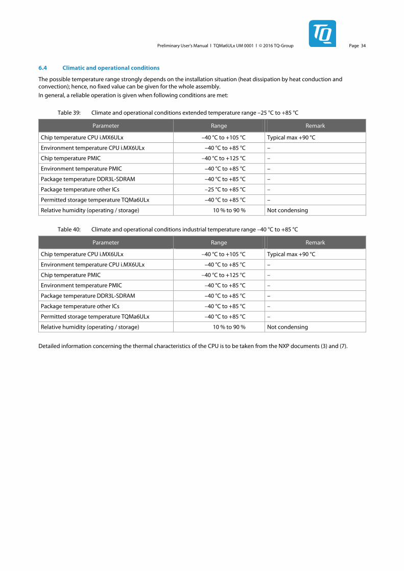
Preliminary User's Manual l TQMa6ULx UM 0001 l © 2016 TQ-Group Page 34
6.4 Climatic and operational conditions
The possible temperature range strongly depends on the installation situation (heat dissipation by heat conduction and convection); hence, no fixed value can be given for the whole assembly.
In general, a reliable operation is given when following conditions are met:
Table 39: Climate and operational conditions extended temperature range –25 °C to +85 °C
Parameter Range Remark
Chip temperature CPU i.MX6ULx –40 °C to +105 °C Typical max +90 °C
Environment temperature CPU i.MX6ULx –40 °C to +85 °C –
Chip temperature PMIC –40 °C to +125 °C –
Environment temperature PMIC –40 °C to +85 °C –
Package temperature DDR3L-SDRAM –40 °C to +85 °C –
Package temperature other ICs –25 °C to +85 °C –
Permitted storage temperature TQMa6ULx –40 °C to +85 °C –
Relative humidity (operating / storage) 10 % to 90 % Not condensing
Table 40: Climate and operational conditions industrial temperature range –40 °C to +85 °C
Parameter Range Remark
Chip temperature CPU i.MX6ULx –40 °C to +105 °C Typical max +90 °C
Environment temperature CPU i.MX6ULx –40 °C to +85 °C –
Chip temperature PMIC –40 °C to +125 °C –
Environment temperature PMIC –40 °C to +85 °C –
Package temperature DDR3L-SDRAM –40 °C to +85 °C –
Package temperature other ICs –40 °C to +85 °C –
Permitted storage temperature TQMa6ULx –40 °C to +85 °C –
Relative humidity (operating / storage) 10 % to 90 % Not condensing
Detailed information concerning the thermal characteristics of the CPU is to be taken from the NXP documents (3) and (7).
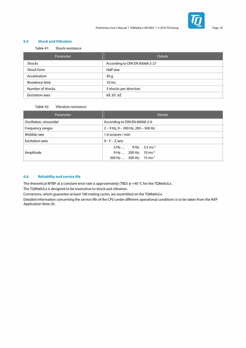
Preliminary User's Manual l TQMa6ULx UM 0001 l © 2016 TQ-Group Page 35
6.5 Shock and Vibration
Table 41: Shock resistance
Parameter Details
Shocks According to DIN EN 60068-2-27
Shock form Half sine
Acceleration 30 g
Residence time 10 ms
Number of shocks 3 shocks per direction
Excitation axes 6X, 6Y, 6Z
Table 42: Vibration resistance
Parameter Details
Oscillation, sinusoidal According to DIN EN 60068-2-6
Frequency ranges 2 – 9 Hz, 9 – 200 Hz, 200 – 500 Hz
Wobble rate 1.0 octaves / min
Excitation axes X– Y – Z axis
Amplitude
2 Hz … 9 Hz: 3.5 ms-2
9 Hz … 200 Hz: 10 ms-2
200 Hz … 500 Hz: 15 ms-2
6.6 Reliability and service life
The theoretical MTBF at a constant error rate is approximately (TBD) @ +40 °C for the TQMa6ULx.
The TQMa6ULx is designed to be insensitive to shock and vibration.
Connectors, which guarantee at least 100 mating cycles, are assembled on the TQMa6ULx.
Detailed information concerning the service life of the CPU under different operational conditions is to be taken from the NXP Application Note (4).
Preliminary User's Manual l TQMa6ULx UM 0001 l © 2016 TQ-Group Page 36
7. ENVIRONMENT PROTECTION
7.1 RoHS
The TQMa6ULx is manufactured RoHS compliant.
• All components and assemblies are RoHS compliant
• The soldering processes are RoHS compliant
7.2 WEEE
The company placing the product on the market is responsible for the observance of the WEEE regulation.
To be able to reuse the product, it is produced in such a way (a modular construction) that it can be easily repaired and disassembled.
7.3 REACH
The EU-chemical regulation 1907/2006 (REACH regulation) stands for registration, evaluation, certification and restriction of substances SVHC (Substances of very high concern, e.g., carcinogen, mutagen and/or persistent, bio accumulative and toxic). Within the scope of this juridical liability, TQ-Systems GmbH meets the information duty within the supply chain with regard to the SVHC substances, insofar as suppliers inform TQ-Systems GmbH accordingly.
7.4 EuP
The guideline 2005/32/EC (EuP) is the next step after WEEE® and RoHS for an environmentally friendly production of electric and electronic products. The consideration of environmental requirements with the product design "creation appropriate for the environment" ("ecological design") with the aim to improve the environmental compatibility of the product during its whole life cycle should be taken into consideration. The guideline appropriate for the product (embedded PC) is applied.
7.5 Battery
No batteries are assembled on the TQMa6ULx.
7.6 Packaging
By environmentally friendly processes, production equipment and products, we contribute to the protection of our environment. To be able to reuse the TQMa6ULx, it is produced in such a way (a modular construction) that it can be easily repaired and disassembled. The energy consumption of this subassembly is minimised by suitable measures. The TQMa6ULx is delivered in reusable packaging.
7.7 Other entries
The energy consumption of this subassembly is minimised by suitable measures.
Because currently there is still no technical equivalent alternative for printed circuit boards with bromine-containing flame protection (FR-4 material), such printed circuit boards are still used.
No use of PCB containing capacitors and transformers (polychlorinated biphenyls).
These points are an essential part of the following laws:
• The law to encourage the circular flow economy and assurance of the environmentally acceptable removal of waste as at 27.9.94 (Source of information: BGBl I 1994, 2705)
• Regulation with respect to the utilization and proof of removal as at 1.9.96 (Source of information: BGBl I 1996, 1382, 1997, 2860)
• Regulation with respect to the avoidance and utilization of packaging waste as at 21.8.98 (Source of information: BGBl I 1998, 2379)
• Regulation with respect to the European Waste Directory as at 1.12.01 (Source of information: BGBl I 2001, 3379)
This information is to be seen as notes. Tests or certifications were not carried out in this respect.
Preliminary User's Manual l TQMa6ULx UM 0001 l © 2016 TQ-Group Page 37
8. APPENDIX
8.1 Acronyms and definitions
The following acronyms and abbreviations are used in this document:
Table 43: Acronyms
Acronym Meaning
8.2 References
Table 44: Further applicable documents
No. Name Rev., Date Company
(1) i.MX 6UltraLite Applications Processors for Industrial Products IMX6ULxIEC_rev1.pdf Rev. 1, 04/2016 NXP
(2) Chip Errata for the i.MX 6UltraLite IMX6ULxCE_rev1.pdf Rev. 1, 04/2016 NXP
(3) i.MX 6UltraLite Power Consumption Measurement AN5170_power_rev2.pdf Rev. 2, 05/2016 NXP
(4) i.MX 6UltraLite Product Usage Lifetime Estimates AN5198_life_rev1.pdf Rev. 1, 04/2016 NXP
(5) Hardware Development Guide for the i.MX 6UltraLite Applications Processor IMX6ULxHDG_rev1.pdf Rev. 1, 03/2016 NXP
(6) i.MX 6UltraLite Applications Processor Reference Manual IMX6ULxRM_rev1.pdf Rev. 1, 04/2016 NXP
(7) Power management integrated circuit (PMIC) for i.MX7 & i.MX 6SL/SX/UL Rev. 7, 03/2016 NXP
(8) MBa6ULx Preliminary User's Manual – current – TQ-Systems
(9) Support-Wiki for the TQMa6ULx – current – TQ-Systems
(10)