Embed Size (px)
Citation preview
Chapter 7
Tracking of SpreadSpectrum Signals
7.1 Introduction
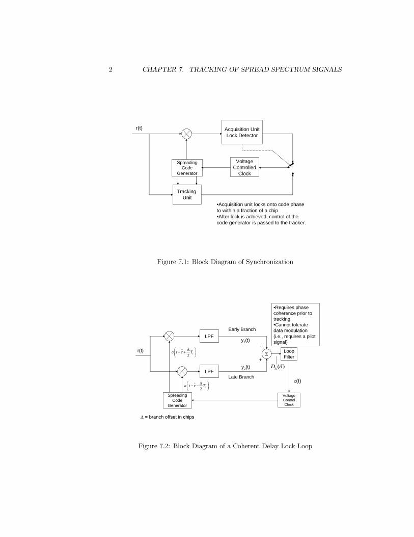
As discussed in the last chapter, there are two parts to the synchronizationprocess. The first stage is often termed acquisition and typically obtains initial,coarse timing synchronization. The second is termed tracking and involves finetuning the delay estimate. Tracking occurs throughout the duration of thecommunication. This procedure is presented in Figure 7.1.
In this chapter we will investigate code tracking. Code tracking is analo-gous to phase tracking in conventional digital communication systems. Muchof the analysis can be directly borrowed from phase tracking analysis. Thereare several well-known techniques for performing tracking including the DelayLock Loop (DLL), the Tau-Dither Loop, and the Double-Dither Loop. In thischapter we will focus on the Delay Lock Loop.
7.2 The Delay Lock Loop
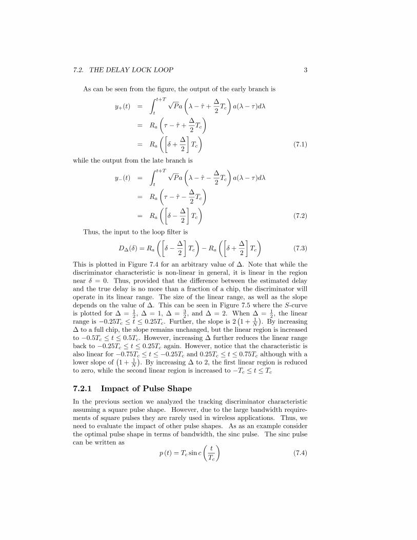
Perhaps the most common form of tracking is the delay lock loop or what is oftentermed the Early-Late Gate. The coherent Early-Late Gate is plotted in Figure7.2. The basic idea behind the circuit is that if we attempt to despread thesignal with a version of the spreading code that is either early or late, we obtainless then full energy. The difference between these two despreader outputs (onaverage) tells us whether the current timing is ahead or behind the true delay.To understand this consider Figure 7.2.
1
2 CHAPTER 7. TRACKING OF SPREAD SPECTRUM SIGNALS
Acquisition UnitLock Detector
Tracking Unit
r(t)
SpreadingCode
Generator
VoltageControlled
Clock
•Acquisition unit locks onto code phase to within a fraction of a chip•After lock is achieved, control of the code generator is passed to the tracker.
Figure 7.1: Block Diagram of Synchronization
SpreadingCode
Generator
LPF
LPF
Σ
-
+
LoopFilter
VoltageControlClock
r(t)
ε(t)
•Requires phase coherence prior to tracking•Cannot tolerate data modulation (i.e., requires a pilot signal)
Late Branch
Early Branch
2 ca t Tτ ∆⎛ ⎞− −⎜ ⎟⎝ ⎠
2 ca t Tτ ∆⎛ ⎞− +⎜ ⎟⎝ ⎠
( )D δ∆
∆ = branch offset in chips
y1(t)
y2(t)
Figure 7.2: Block Diagram of a Coherent Delay Lock Loop
7.2. THE DELAY LOCK LOOP 3
As can be seen from the figure, the output of the early branch is
y+(t) =
Z t+T
t
√Pa
µλ− τ̂ +
∆
2Tc
¶a(λ− τ)dλ
= Ra
µτ − τ̂ +
∆
2Tc
¶= Ra
µ∙δ +
∆
2
¸Tc
¶(7.1)
while the output from the late branch is
y−(t) =
Z t+T
t
√Pa
µλ− τ̂ − ∆
2Tc
¶a(λ− τ)dλ
= Ra
µτ − τ̂ − ∆
2Tc
¶= Ra
µ∙δ − ∆
2
¸Tc
¶(7.2)
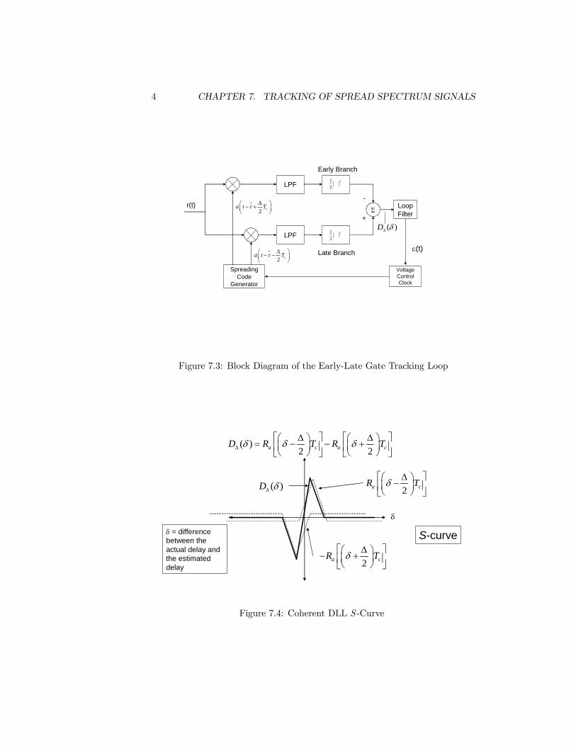
Thus, the input to the loop filter is
D∆(δ) = Ra
µ∙δ − ∆
2
¸Tc
¶−Ra
µ∙δ +
∆
2
¸Tc
¶(7.3)
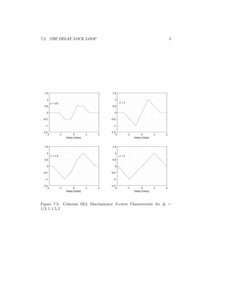
This is plotted in Figure 7.4 for an arbitrary value of ∆. Note that while thediscriminator characteristic is non-linear in general, it is linear in the regionnear δ = 0. Thus, provided that the difference between the estimated delayand the true delay is no more than a fraction of a chip, the discriminator willoperate in its linear range. The size of the linear range, as well as the slopedepends on the value of ∆. This can be seen in Figure 7.5 where the S-curveis plotted for ∆ = 1
2 , ∆ = 1, ∆ = 32 , and ∆ = 2. When ∆ = 1
2 , the linearrange is −0.25Tc ≤ t ≤ 0.25Tc. Further, the slope is 2
¡1 + 1
N
¢. By increasing
∆ to a full chip, the slope remains unchanged, but the linear region is increasedto −0.5Tc ≤ t ≤ 0.5Tc. However, increasing ∆ further reduces the linear rangeback to −0.25Tc ≤ t ≤ 0.25Tc again. However, notice that the characteristic isalso linear for −0.75Tc ≤ t ≤ −0.25Tc and 0.25Tc ≤ t ≤ 0.75Tc although with alower slope of
¡1 + 1
N
¢. By increasing ∆ to 2, the first linear region is reduced
to zero, while the second linear region is increased to −Tc ≤ t ≤ Tc
7.2.1 Impact of Pulse Shape
In the previous section we analyzed the tracking discriminator characteristicassuming a square pulse shape. However, due to the large bandwidth require-ments of square pulses they are rarely used in wireless applications. Thus, weneed to evaluate the impact of other pulse shapes. As as an example considerthe optimal pulse shape in terms of bandwidth, the sinc pulse. The sinc pulsecan be written as
p (t) = Tc sin c
µt
Tc
¶(7.4)
4 CHAPTER 7. TRACKING OF SPREAD SPECTRUM SIGNALS
SpreadingCode
Generator
LPF
LPF 212
212
Σ
-
+
LoopFilter
VoltageControlClock
r(t)
ε(t)Late Branch
Early Branch
2 ca t Tτ ∆⎛ ⎞− −⎜ ⎟⎝ ⎠
2 ca t Tτ ∆⎛ ⎞− +⎜ ⎟⎝ ⎠
( )D δ∆
Figure 7.3: Block Diagram of the Early-Late Gate Tracking Loop
( )2 2a c a cD R T R Tδ δ δ∆
⎡ ∆ ⎤ ⎡ ∆ ⎤⎛ ⎞ ⎛ ⎞= − − +⎜ ⎟ ⎜ ⎟⎢ ⎥ ⎢ ⎥⎝ ⎠ ⎝ ⎠⎣ ⎦ ⎣ ⎦
2a cR Tδ⎡ ∆ ⎤⎛ ⎞−⎜ ⎟⎢ ⎥⎝ ⎠⎣ ⎦
2a cR Tδ⎡ ∆ ⎤⎛ ⎞− +⎜ ⎟⎢ ⎥⎝ ⎠⎣ ⎦
( )D δ∆
S-curve
δ
δ = difference between the actual delay and the estimated delay
Figure 7.4: Coherent DLL S -Curve
7.2. THE DELAY LOCK LOOP 5
-2 -1 0 1 2-1.5
-1
-0.5
0
0.5
1
1.5
Delay (chips)-2 -1 0 1 2
-1.5
-1
-0.5
0
0.5
1
1.5
Delay (chips)
-2 -1 0 1 2-1.5
-1
-0.5
0
0.5
1
1.5
Delay (chips)-2 -1 0 1 2
-1.5
-1
-0.5
0
0.5
1
1.5
Delay (chips)
∆ = 1/2 ∆ = 1
∆ = 1.5 ∆ = 2
Figure 7.5: Coherent DLL Discriminator S -curve Characteristic for ∆ =1/2, 1, 1.5, 2
6 CHAPTER 7. TRACKING OF SPREAD SPECTRUM SIGNALS
As discussed in Chapter 5, the autocorrelation of the spreading waveform isdominated by the pulse autocorrelation function. We can find the autocorrela-tion function of the sinc pulse as
Rp (τ) = p (t) ∗ p (−t) (7.5)
= p (t) ∗ p (t) (7.6)
where the second line results from the fact that the sinc pulse is symmetric.Using the Fourier Transform, we can write
Rp (τ) = F−1 {P (f)P (f)} (7.7)
where P (f) is the Fourier Transform of the pulse shape. Thus, we can write
Rp (τ) = F−1 {rec (fTc) rec (fTc)} (7.8)
= F−1 {rec (fTc)} (7.9)
= Tc sin c
µt
Tc
¶(7.10)
Thus, the autocorrelation function is the same as the pulse shape. Assuming
the ideal sequence autocorrelation Caa(n) =
½1 n = 00 n 6= 0 , the discriminator
characteristic can be written as
D∆(δ) = Rp
µ∙δ − ∆
2
¸Tc
¶−Rp
µ∙δ +
∆
2
¸Tc
¶(7.11)
= sin c
µ∙δ − ∆
2
¸¶− sin c
µ∙δ +
∆
2
¸¶(7.12)
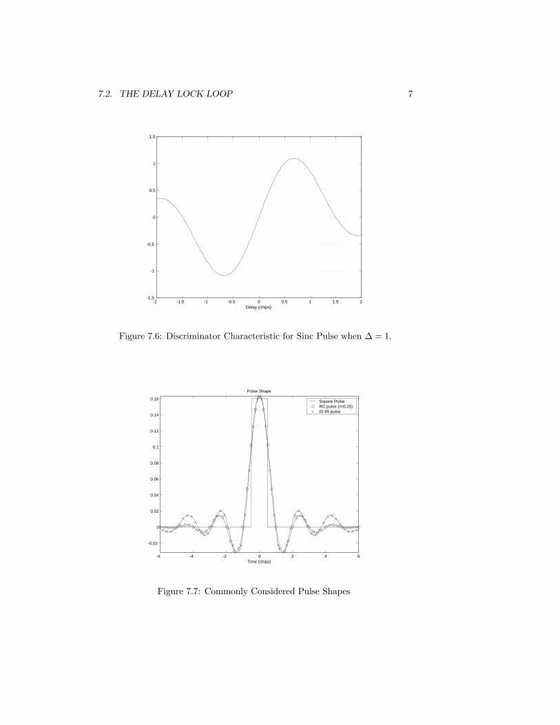
The resulting characteristic is plotted in Figure 7.6. We can see that like thesquare pulse, there exists a nearly linear region with a slope of approximately2 over the range
¡−12 ,
12
¢. Like in the case of a square pulse, the discriminator
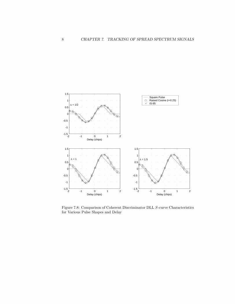
will work properly provided that the error stays within this linear region.Further, consider two additional pulses that are commonly used the raised
cosine pulse (roll-off factor of 0.25) and the pulse used in the IS-95 standard[1]. The pulses are plotted along with a square pulse in Figure 7.7. Usingthe same development as shown above for the sinc pulse, we can derive theautocorrelation fuction and the resulting discriminator characteristic for eachof the pulse shapes. The discriminator characteristic for each pulse is given inFigure 7.8 for ∆ = 1, ∆ = 1/2, and ∆ = 3/2 respectively. We can see that theother pulse shapes provide similar trends as the square pulse. Setting ∆ = 1provides the best characteristic as ∆ = 1/2 impacts the size and slope of thelinear region while ∆ = 1.5 slightly distorts the linear region.
7.2. THE DELAY LOCK LOOP 7
-2 -1.5 -1 -0.5 0 0.5 1 1.5 2-1.5
-1
-0.5
0
0.5
1
1.5
Delay (chips)
Figure 7.6: Discriminator Characteristic for Sinc Pulse when ∆ = 1.
-6 -4 -2 0 2 4 6
-0.02
0
0.02
0.04
0.06
0.08
0.1
0.12
0.14
0.16
Time (chips)
Pulse Shape
Square PulseRC pulse (r=0.25)IS-95 pulse
Figure 7.7: Commonly Considered Pulse Shapes
8 CHAPTER 7. TRACKING OF SPREAD SPECTRUM SIGNALS
-2 -1 0 1 2-1.5
-1
-0.5
0
0.5
1
1.5
Delay (chips)
Square PulseRaised Cosine (r=0.25)IS-95
-2 -1 0 1 2-1.5
-1
-0.5
0
0.5
1
1.5
Delay (chips)-2 -1 0 1 2
-1.5
-1
-0.5
0
0.5
1
1.5
Delay (chips)
∆ = 1/2
∆ = 1 ∆ = 1.5
Figure 7.8: Comparison of Coherent Discriminator DLL S -curve Characteristicsfor Various Pulse Shapes and Delay
7.3. THE NON-COHERENT DELAY LOCK LOOP 9
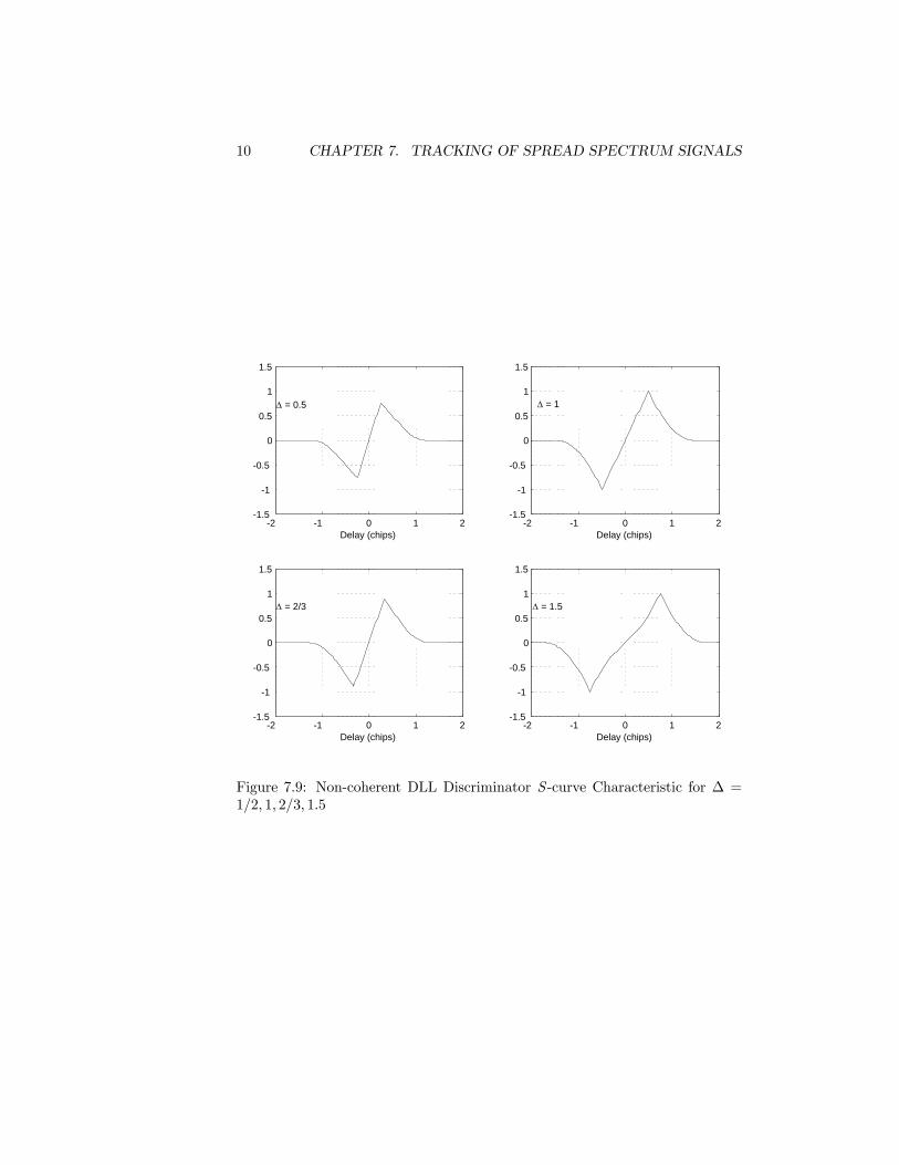
7.3 The Non-coherent Delay Lock LoopA main limitation of the coherent delay lock loop is that it cannot tolerate datamodulation. Thus, it requires a pilot signal for proper operation. In many casespilot signals cannot be afforded since they result in wasted power. A solutionto this problem is the non-coherent delay lock loop shown in Figure ??. In thisloop, the output of the despreading operation on both the early and the latebranch are squared prior to subtracting the early result from the late result.While this changes the discriminator characteristic, it still results in a linearregion around δ = 0 and thus allows for proper operation. Specifically thediscriminator characteristic is [2]
D∆(δ) = R2a
µ∙δ − ∆
2
¸Tc
¶−R2a
µ∙δ +
∆
2
¸Tc
¶(7.13)
For ∆ ≥ 1, this results in
∆a(δ) =
⎧⎪⎪⎪⎪⎪⎪⎪⎨⎪⎪⎪⎪⎪⎪⎪⎩
0 −N + 1 + ∆2 < δ ≤ −
¡1 + ∆
2
¢1N2 −
£1 +
¡1 + 1
N
¢ ¡δ + ∆
2
¢¤2 −¡1 + ∆
2
¢< δ ≤ −∆2
1N2 −
£1−
¡1 + 1
N
¢ ¡δ + ∆
2
¢¤2 −∆2 < δ ≤ −¡1− ∆2
¢2¡1 + 1
N
¢ £2−
¡1 + 1
N
¢∆¤δ −
¡1− ∆2
¢< δ ≤
¡1− ∆2
¢£1 +
¡1 + 1
N
¢ ¡δ − ∆2
¢¤2 − 1N2
¡1− ∆2
¢< δ ≤ ∆
2£1−
¡1 + 1
N
¢ ¡δ − ∆2
¢¤2 − 1N2
∆2 < δ ≤
¡1 + ∆
2
¢(7.14)
For ∆ ≤ 1 the discriminator characteristic is
∆a(δ) =
⎧⎪⎪⎪⎪⎪⎪⎪⎨⎪⎪⎪⎪⎪⎪⎪⎩
0 −N + 1 + ∆2 < δ ≤ −
¡1 + ∆
2
¢1N2 −
£1 +
¡1 + 1
N
¢ ¡δ + ∆
2
¢¤2 −¡1 + ∆
2
¢< δ ≤ −
¡1− ∆2
¢−2¡1 + 1
N
¢∆£1 +
¡1 + 1
N
¢δ¤
−¡1− ∆2
¢< δ ≤ −∆2
2¡1 + 1
N
¢ £2−
¡1 + 1
N
¢∆¤δ −∆2 < δ ≤ ∆
2
2¡1 + 1
N
¢∆£1 +
¡1 + 1
N
¢δ¤
∆2 < δ ≤ 1− ∆2£
1 +¡1 + 1
N
¢ ¡δ + ∆
2
¢¤2 − 1N2
1−∆2 < δ ≤
¡1 + ∆
2
¢(7.15)
As can be seen, the region around δ = 0 is linear. The size of the linear regiondepends on the value of ∆. For ∆ > 1, the linear region is −
¡1− ∆2
¢< δ ≤¡
1− ∆2¢whereas when ∆ ≤ 1, the region is −∆2 < δ ≤ ∆
2 . In either case, we seethat the linear region is maximized when ∆ = 1. Examples of the Non-coherentDLL discriminator characteristic are plotted in Figure 7.9
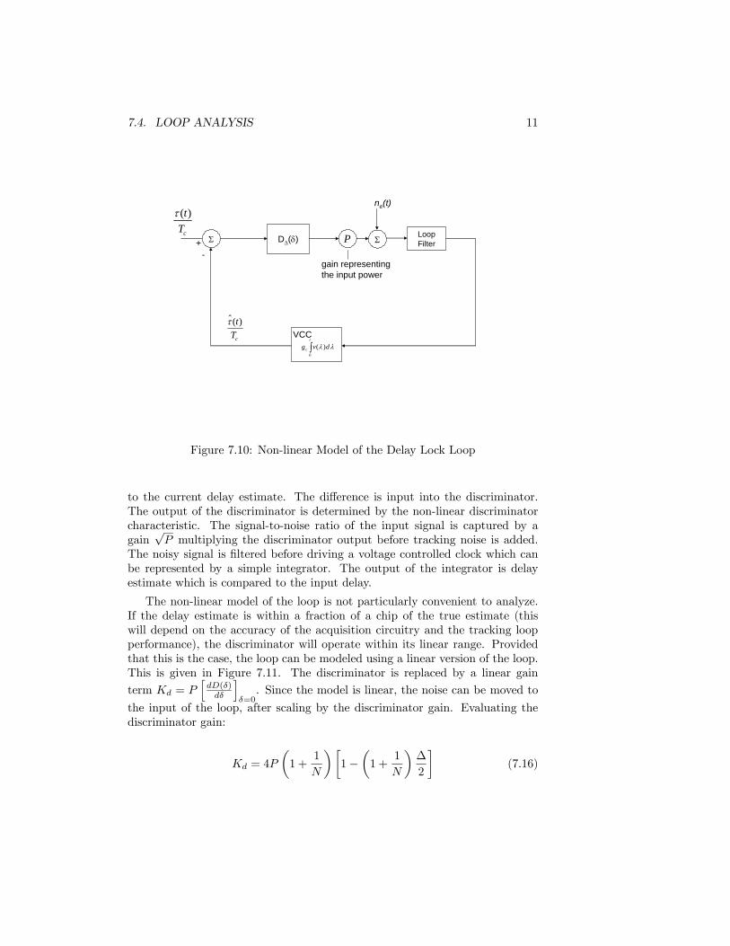
7.4 Loop AnalysisIn order to analyze the performance of the delay lock loop we must create amodel for the delay and the resulting tracking error. A straightforward non-linear model of the loop is presented in Figure 7.10. The time varying delay ofthe signal normalized by the chip period comes into the loop and is the compared
10 CHAPTER 7. TRACKING OF SPREAD SPECTRUM SIGNALS
-2 -1 0 1 2-1.5
-1
-0.5
0
0.5
1
1.5
Delay (chips)-2 -1 0 1 2
-1.5
-1
-0.5
0
0.5
1
1.5
Delay (chips)
-2 -1 0 1 2-1.5
-1
-0.5
0
0.5
1
1.5
Delay (chips)-2 -1 0 1 2
-1.5
-1
-0.5
0
0.5
1
1.5
Delay (chips)
∆ = 0.5
∆ = 2/3
∆ = 1
∆ = 1.5
Figure 7.9: Non-coherent DLL Discriminator S -curve Characteristic for ∆ =1/2, 1, 2/3, 1.5
7.4. LOOP ANALYSIS 11
D∆(δ) LoopFilterΣ Σ
VCC
0
( )t
cg v dλ λ∫
ne(t)
P+-
( )
c
tTτ
( )
c
tTτ
gain representing the input power
Figure 7.10: Non-linear Model of the Delay Lock Loop
to the current delay estimate. The difference is input into the discriminator.The output of the discriminator is determined by the non-linear discriminatorcharacteristic. The signal-to-noise ratio of the input signal is captured by again
√P multiplying the discriminator output before tracking noise is added.
The noisy signal is filtered before driving a voltage controlled clock which canbe represented by a simple integrator. The output of the integrator is delayestimate which is compared to the input delay.
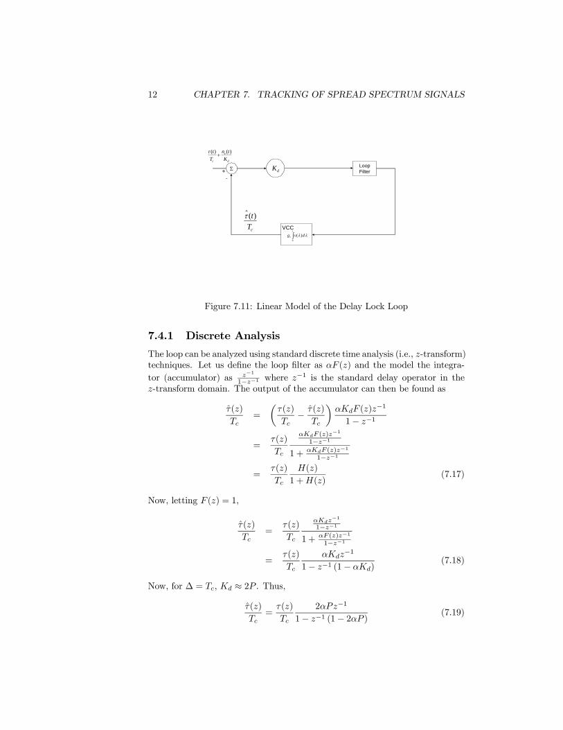
The non-linear model of the loop is not particularly convenient to analyze.If the delay estimate is within a fraction of a chip of the true estimate (thiswill depend on the accuracy of the acquisition circuitry and the tracking loopperformance), the discriminator will operate within its linear range. Providedthat this is the case, the loop can be modeled using a linear version of the loop.This is given in Figure 7.11. The discriminator is replaced by a linear gainterm Kd = P
hdD(δ)dδ
iδ=0. Since the model is linear, the noise can be moved to
the input of the loop, after scaling by the discriminator gain. Evaluating thediscriminator gain:
Kd = 4P
µ1 +
1
N
¶ ∙1−
µ1 +
1
N
¶∆
2
¸(7.16)
12 CHAPTER 7. TRACKING OF SPREAD SPECTRUM SIGNALS
LoopFilterΣ
VCC
0
( )t
cg v dλ λ∫
dK+-
( )( ) e
c d
n ttT Kτ
+
( )
c
tTτ
Figure 7.11: Linear Model of the Delay Lock Loop
7.4.1 Discrete Analysis
The loop can be analyzed using standard discrete time analysis (i.e., z-transform)techniques. Let us define the loop filter as αF (z) and the model the integra-tor (accumulator) as z−1
1−z−1 where z−1 is the standard delay operator in thez-transform domain. The output of the accumulator can then be found as
τ̂(z)
Tc=
µτ(z)
Tc− τ̂(z)
Tc
¶αKdF (z)z
−1
1− z−1
=τ(z)
Tc
αKdF (z)z−1
1−z−1
1 + αKdF (z)z−1
1−z−1
=τ(z)
Tc
H(z)
1 +H(z)(7.17)
Now, letting F (z) = 1,
τ̂(z)
Tc=
τ(z)
Tc
αKdz−1
1−z−1
1 + αF (z)z−1
1−z−1
=τ(z)
Tc
αKdz−1
1− z−1 (1− αKd)(7.18)
Now, for ∆ = Tc, Kd ≈ 2P . Thus,
τ̂(z)
Tc=
τ(z)
Tc
2αPz−1
1− z−1 (1− 2αP ) (7.19)
7.4. LOOP ANALYSIS 13
Thus, for an arbitrary input τ(z) we can determine a loop response τ̂(z). Ad-ditionally, we can compute the loop error response as
τe(z) =
µτ(z)
Tc− τ̂(z)
Tc
¶=
τ(z)
Tc
1− z−1
1− z−1 (1− 2αP ) (7.20)
The main control parameter in this case is the filter gain α. We can decreasethe loop response to noise by decreasing α. However, this also has the effect ofincreasing the loop response time. As an example, consider a step input ∆τTc
τe(z) =∆τ
Tc
1
1− z−11− z−1
1− z−1 (1− 2αP )
=∆τ
Tc
1
1− z−1 (1− 2αP ) (7.21)
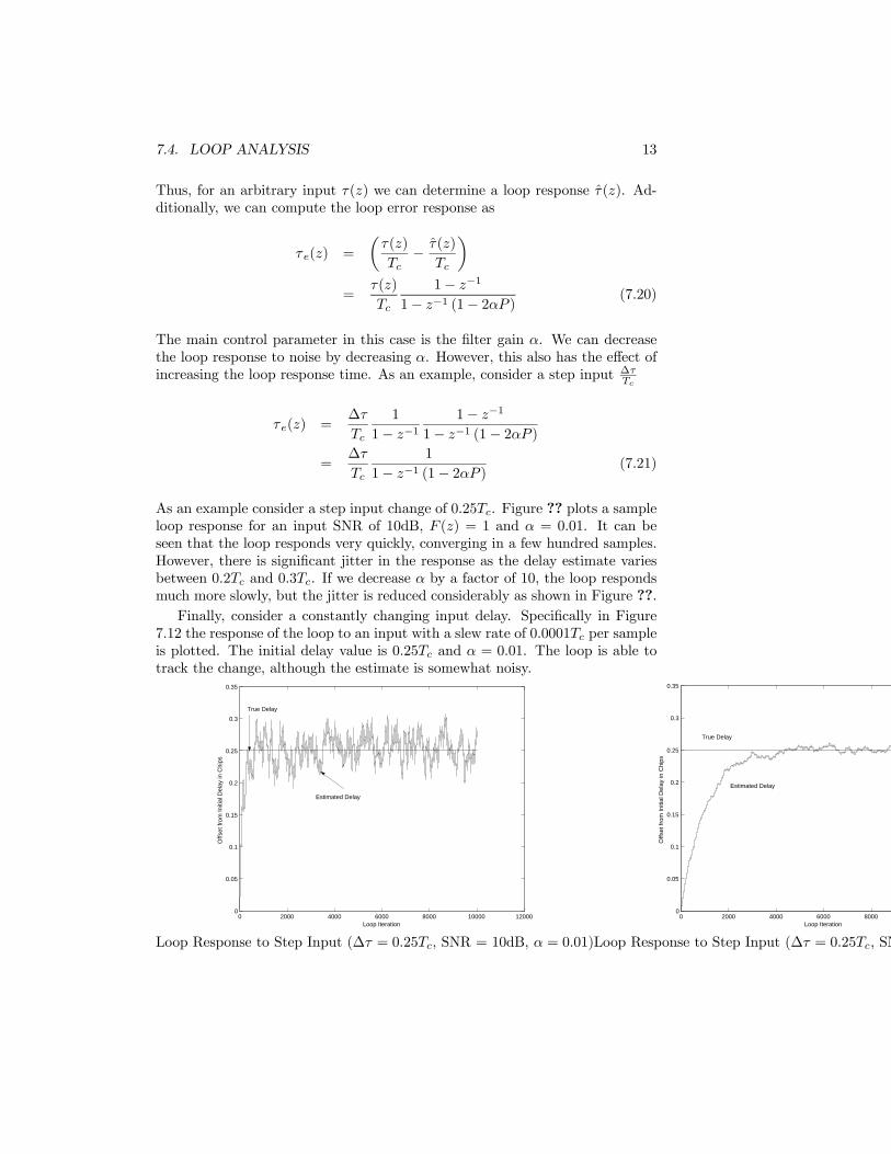
As an example consider a step input change of 0.25Tc. Figure ?? plots a sampleloop response for an input SNR of 10dB, F (z) = 1 and α = 0.01. It can beseen that the loop responds very quickly, converging in a few hundred samples.However, there is significant jitter in the response as the delay estimate variesbetween 0.2Tc and 0.3Tc. If we decrease α by a factor of 10, the loop respondsmuch more slowly, but the jitter is reduced considerably as shown in Figure ??.Finally, consider a constantly changing input delay. Specifically in Figure
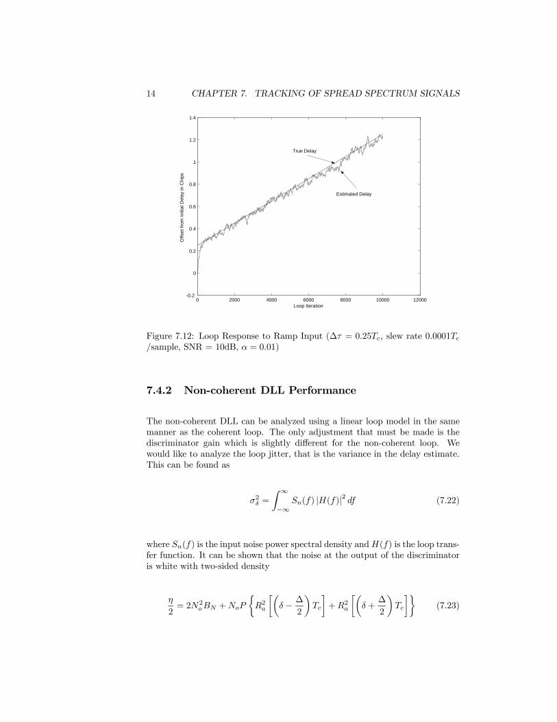
7.12 the response of the loop to an input with a slew rate of 0.0001Tc per sampleis plotted. The initial delay value is 0.25Tc and α = 0.01. The loop is able totrack the change, although the estimate is somewhat noisy.
0 2000 4000 6000 8000 10000 120000
0.05
0.1
0.15
0.2
0.25
0.3
0.35
Loop Iteration
Offs
et fr
om In
itial
Del
ay in
Chi
ps
Estimated Delay
True Delay
Loop Response to Step Input (∆τ = 0.25Tc, SNR = 10dB, α = 0.01)
0 2000 4000 6000 80000
0.05
0.1
0.15
0.2
0.25
0.3
0.35
Loop Iteration
Offs
et fr
om In
itial
Del
ay in
Chi
ps
True Delay
Estimated Delay
Loop Response to Step Input (∆τ = 0.25Tc, SN
14 CHAPTER 7. TRACKING OF SPREAD SPECTRUM SIGNALS
0 2000 4000 6000 8000 10000 12000-0.2
0
0.2
0.4
0.6
0.8
1
1.2
1.4
Loop Iteration
Offs
et fr
om In
itial
Del
ay in
Chi
ps
True Delay
Estimated Delay
Figure 7.12: Loop Response to Ramp Input (∆τ = 0.25Tc, slew rate 0.0001Tc/sample, SNR = 10dB, α = 0.01)
7.4.2 Non-coherent DLL Performance
The non-coherent DLL can be analyzed using a linear loop model in the samemanner as the coherent loop. The only adjustment that must be made is thediscriminator gain which is slightly different for the non-coherent loop. Wewould like to analyze the loop jitter, that is the variance in the delay estimate.This can be found as
σ2δ =
Z ∞−∞
Sn(f) |H(f)|2 df (7.22)
where Sn(f) is the input noise power spectral density andH(f) is the loop trans-fer function. It can be shown that the noise at the output of the discriminatoris white with two-sided density
η
2= 2N2
oBN +NoP
½R2a
∙µδ − ∆
2
¶Tc
¸+R2a
∙µδ +
∆
2
¶Tc
¸¾(7.23)
7.4. LOOP ANALYSIS 15
Now the jitter is then σ2δ =η21K2dWL whereWL is the two-sided loop bandwidth.
Assuming that ∆ = Tc, N >> 1, and δ 0,
η
2= 2N2
oBN +NoP
½R2a
∙µδ − ∆
2
¶Tc
¸+R2a
∙µδ +
∆
2
¶Tc
¸¾= 2N2
oBN +NoP
½R2a
∙µ−∆2
¶Tc
¸+R2a
∙µ+∆
2
¶Tc
¸¾= 2N2
oBN +NoP
(2
µ1− ∆
2
¶2)= 2N2
oBN +1
2NoP (7.24)
Returning to the equation for loop jitter
σ2δ =
µ2N2
oBN +1
2NoP
¶1
K2d
WL (7.25)
The gain of the discriminator characteristic can be found to be
Kd = 2P
∙1− ∆
2
¸(7.26)
Thus, letting ∆ = 1
σ2δ =
µ2N2
oBN +1
2NoP
¶1¡
2P£1− ∆2
¤¢2WL
=
µ2N2
oBN +1
2NoP
¶1
P 2WL
=
µ4NoBN
P+ 1
¶No
2PWL
=
µ4
ρIF+ 1
¶1
ρL(7.27)
where ρL is the loop SNR and ρIF is the SNR at the IF bandpass filter. Ingeneral (any value of ∆) the jitter is
σ2δ =
Ã1
ρIF¡1− ∆2
¢2 + 1!1
ρL(7.28)
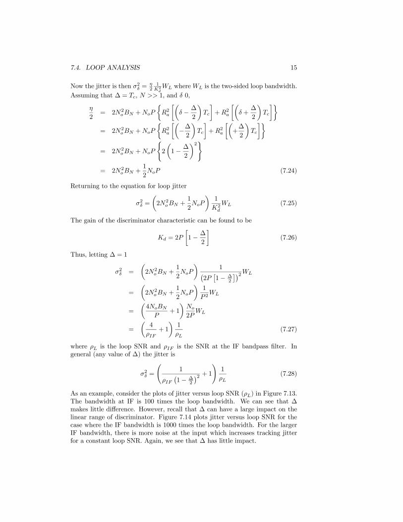
As an example, consider the plots of jitter versus loop SNR (ρL) in Figure 7.13.The bandwidth at IF is 100 times the loop bandwidth. We can see that ∆makes little difference. However, recall that ∆ can have a large impact on thelinear range of discriminator. Figure 7.14 plots jitter versus loop SNR for thecase where the IF bandwidth is 1000 times the loop bandwidth. For the largerIF bandwidth, there is more noise at the input which increases tracking jitterfor a constant loop SNR. Again, we see that ∆ has little impact.
16 CHAPTER 7. TRACKING OF SPREAD SPECTRUM SIGNALS
10 12 14 16 18 20 22 24 26 28 3010-4
10-3
10-2
10-1
100
101
Loop SNR (dB)
Trac
king
Jitt
er (c
hips
)
∆ = 1 ∆ = 0.5∆ = 0.1
Figure 7.13: Example of Timing Jitter (BIF = 100BL, SNR = 10dB, α = 0.01)
10 12 14 16 18 20 22 24 26 28 3010-4
10-3
10-2
10-1
100
101
Loop SNR (dB)
Trac
king
Jitt
er (c
hips
)
∆ = 1 ∆ = 0.5∆ = 0.1
Figure 7.14: Example of Timing Jitter (BIF = 1000BL, SNR = 10dB, α = 0.01)
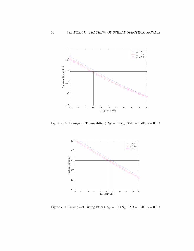
7.5. LAPLACE ANALYSIS 17
7.5 Laplace AnalysisAnother technique for investigating the performance of a tracking loop is toinvestigate it in the analog domain via the Laplace transform. The linear modelfor the delay lock loop in the Laplace domain is presented in Figure 7.15. Themodel is similar to the discrete domain version with the exception that theintegrator is now represented by 1
s and all transforms are in the Laplace domain.The transfer function of the loop H(s) = fracτ̂(s)τ(s) can be found from
the linear model. Specifically,
τ̂(s)
Tc= KdF (s)
gcs
½τ(s)
Tc− τ̂
(s)Tc
¾τ̂(s)
Tc=
½1 +KdF (s)
gcs
τ(s)
Tc
¾(7.29)
Solving for H(s) results in
H(s) =KdF (s)gc
1 +KdF (s)gc(7.30)
We can also easily find the tracking error with respect to the input signal as
E(s) =τ(s)
Tc− τ̂(s)
Tc
=τ(s)
Tc[1−H(s)]
=τ(s)
Tc
s
s+KdgcF (s)(7.31)
We are interested in two aspects of the error signal: the steady state errorand the response time. We would like to examine the impact that F (s) has onthese two items. We shall first examine the steady state error. The steady stateerror can be found as lims←0 sE(s). Let us first consider a step change to thedelay: τ(t) = Au(t). The steady state error e can be found as
e = lims←0
sE(s)
= lims←0
sτ(s)
Tc
s
s+KdgcF (s)
= lims←0
sA
s
s
s+KdgcF (s)
= lims←0
As
s+KdgcF (s)
= 0 (7.32)
Thus, for a step input the loop will eventually track the change regardless ofthe loop filter forcing the steady state error to zero.
18 CHAPTER 7. TRACKING OF SPREAD SPECTRUM SIGNALS
Loop FilterF(s)Σ
VCCcg
s
dK+-
( )
c
sTτ
( )
c
sTτ
Figure 7.15: A Linear Model of the Coherent Delay Lock Loop in the LaplaceTransform Domain
To find the error response, let us first examine the all pass filter F (s) = 1.The error is then
E(s) =τ(s)
Tc
s
s+KdgcF (s)
=A
s
s
s+KdgcF (s)
=A
s+KdgcF (s)(7.33)
Taking the inverse Laplace transform
e(t) = Ae−Kdgct (7.34)
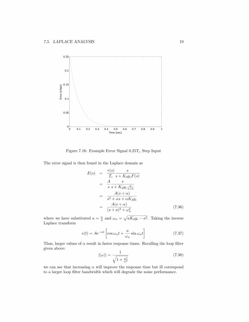
Thus, we can see again that the error will eventually decay to zero. The rateof decay depends on the discriminator gain and the integrator constant. Anexample is plotted in Figure 7.16 for an all pass filter and a step input of 0.25Tc.In the example, ∆ = 1 and SNR = 10.
As a second case let us examine a low pass filter as the loop filter. That is
F (s) =α
s+ α(7.35)
7.5. LAPLACE ANALYSIS 19
0 0.1 0.2 0.3 0.4 0.5 0.6 0.7 0.8 0.9 10
0.05
0.1
0.15
0.2
0.25
Time (sec)
Erro
r (ch
ips)
Figure 7.16: Example Error Signal 0.25Tc Step Input
The error signal is then found in the Laplace domain as
E(s) =τ(s)
Tc
s
s+KdgcF (s)
=A
s
s
s+Kdgcα
s+α
=A(s+ α)
s2 + αs+ αKdgc
=A(s+ α)
(s+ a)2 + ω2n(7.36)
where we have substituted a = α2 and ωn =
paKdgc − a2. Taking the inverse
Laplace transform
e(t) = Ae−at∙cosωnt+
a
ωnsinωnt
¸(7.37)
Thus, larger values of α result in faster response times. Recalling the loop filtergiven above:
|(ω)| = 1q1 + ω2
α2
(7.38)
we can see that increasing α will improve the response time but ill correspondto a larger loop filter bandwidth which will degrade the noise performance.
20 CHAPTER 7. TRACKING OF SPREAD SPECTRUM SIGNALS
0 0.005 0.01 0.015 0.02 0.025 0.03 0.035 0.04 0.045 0.05-0.1
-0.05
0
0.05
0.1
0.15
0.2
0.25
0.3
Time (s)
Erro
r (ch
ips)
Figure 7.17: Example Error Signal with Reduced Bandwidth Filter
0 0.005 0.01 0.015 0.02 0.025 0.03 0.035 0.04 0.045 0.05
-0.25
-0.2
-0.15
-0.1
-0.05
0
0.05
0.1
0.15
0.2
0.25
Time (s)
Erro
r (ch
ips)
Figure 7.18:
7.5. LAPLACE ANALYSIS 21
0 1000 2000 3000 4000 5000 6000 7000 8000 9000 10000-20
-15
-10
-5
0
5
10
Frequency (Hz)
Mag
nitu
de R
espo
nse
α = 1000α = 100
Figure 7.19: Comparison of Filter Magnitude Responses for Example
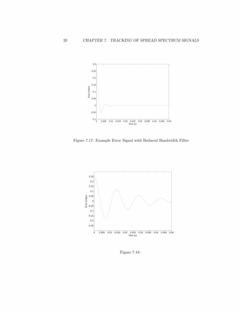
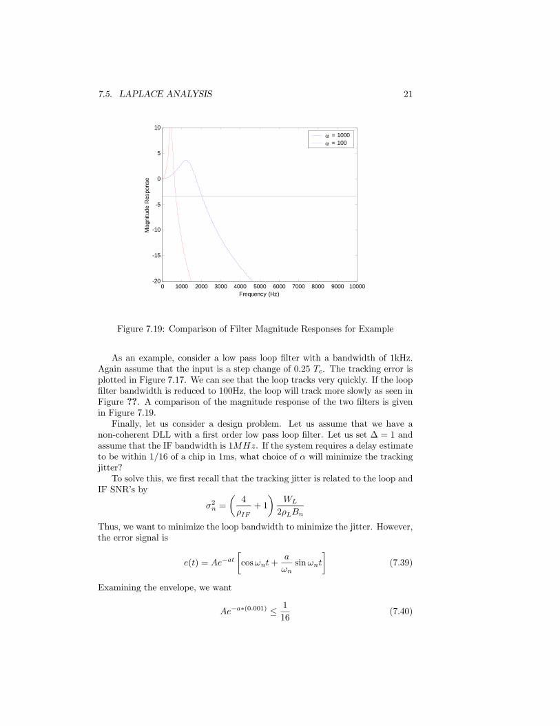
As an example, consider a low pass loop filter with a bandwidth of 1kHz.Again assume that the input is a step change of 0.25 Tc. The tracking error isplotted in Figure 7.17. We can see that the loop tracks very quickly. If the loopfilter bandwidth is reduced to 100Hz, the loop will track more slowly as seen inFigure ??. A comparison of the magnitude response of the two filters is givenin Figure 7.19.Finally, let us consider a design problem. Let us assume that we have a
non-coherent DLL with a first order low pass loop filter. Let us set ∆ = 1 andassume that the IF bandwidth is 1MHz. If the system requires a delay estimateto be within 1/16 of a chip in 1ms, what choice of α will minimize the trackingjitter?To solve this, we first recall that the tracking jitter is related to the loop and
IF SNR’s by
σ2n =
µ4
ρIF+ 1
¶WL
2ρLBn
Thus, we want to minimize the loop bandwidth to minimize the jitter. However,the error signal is
e(t) = Ae−at∙cosωnt+
a
ωnsinωnt
¸(7.39)
Examining the envelope, we want
Ae−a∗(0.001) ≤ 1
16(7.40)
22 CHAPTER 7. TRACKING OF SPREAD SPECTRUM SIGNALS
0 0.001 0.002 0.003 0.004 0.005 0.006 0.007 0.008 0.009 0.01-0.05
0
0.05
0.1
0.15
0.2
0.25
0.3
Time (s)
Erro
r (ch
ips)
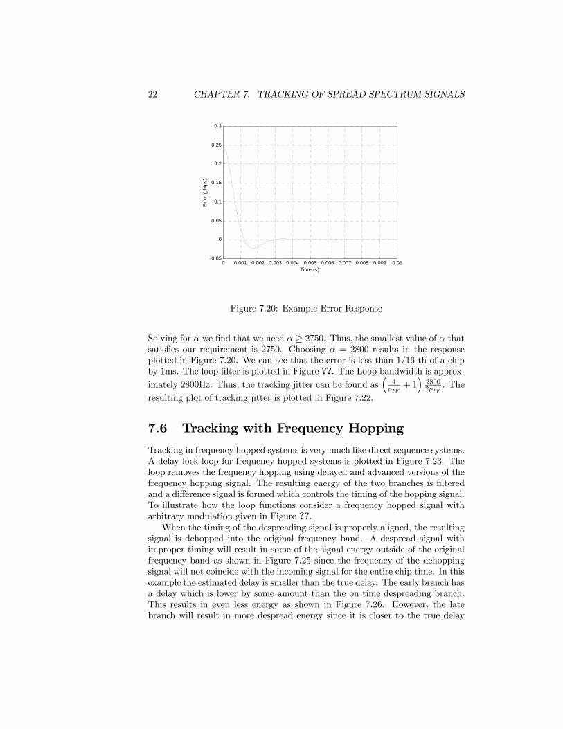
Figure 7.20: Example Error Response
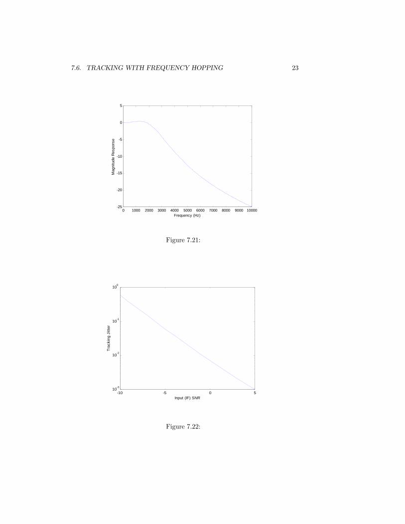
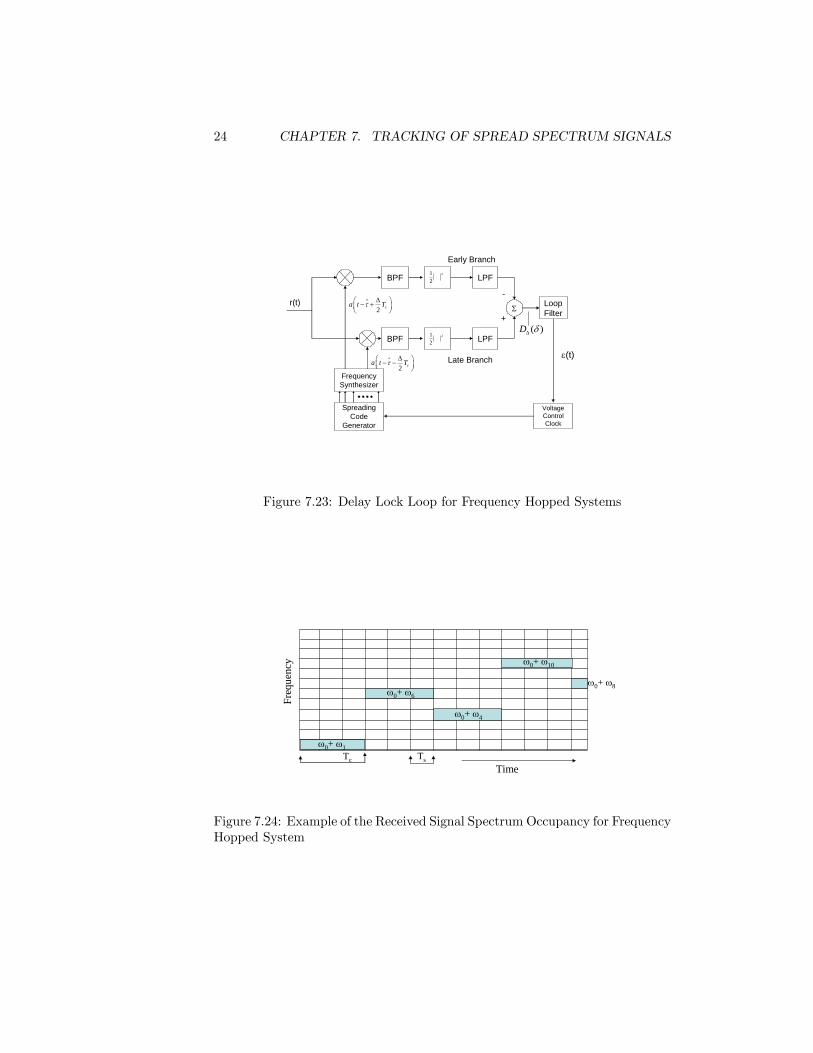
Solving for α we find that we need α ≥ 2750. Thus, the smallest value of α thatsatisfies our requirement is 2750. Choosing α = 2800 results in the responseplotted in Figure 7.20. We can see that the error is less than 1/16 th of a chipby 1ms. The loop filter is plotted in Figure ??. The Loop bandwidth is approx-imately 2800Hz. Thus, the tracking jitter can be found as
³4
ρIF+ 1´28002ρIF
. The
resulting plot of tracking jitter is plotted in Figure 7.22.
7.6 Tracking with Frequency Hopping
Tracking in frequency hopped systems is very much like direct sequence systems.A delay lock loop for frequency hopped systems is plotted in Figure 7.23. Theloop removes the frequency hopping using delayed and advanced versions of thefrequency hopping signal. The resulting energy of the two branches is filteredand a difference signal is formed which controls the timing of the hopping signal.To illustrate how the loop functions consider a frequency hopped signal witharbitrary modulation given in Figure ??.When the timing of the despreading signal is properly aligned, the resulting
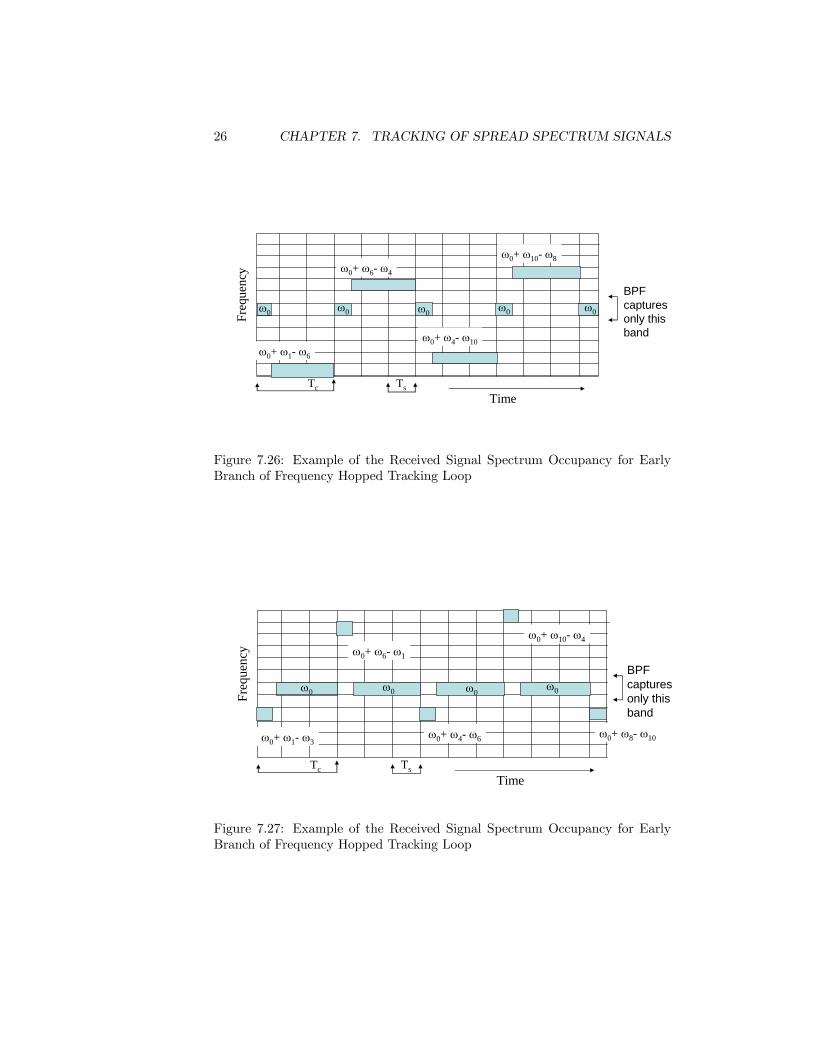
signal is dehopped into the original frequency band. A despread signal withimproper timing will result in some of the signal energy outside of the originalfrequency band as shown in Figure 7.25 since the frequency of the dehoppingsignal will not coincide with the incoming signal for the entire chip time. In thisexample the estimated delay is smaller than the true delay. The early branch hasa delay which is lower by some amount than the on time despreading branch.This results in even less energy as shown in Figure 7.26. However, the latebranch will result in more despread energy since it is closer to the true delay
7.6. TRACKING WITH FREQUENCY HOPPING 23
0 1000 2000 3000 4000 5000 6000 7000 8000 9000 10000-25
-20
-15
-10
-5
0
5
Frequency (Hz)
Mag
nitu
de R
espo
nse
Figure 7.21:
-10 -5 0 510-3
10-2
10-1
100
Input (IF) SNR
Trac
king
Jitt
er
Figure 7.22:
24 CHAPTER 7. TRACKING OF SPREAD SPECTRUM SIGNALS
SpreadingCode
Generator
LPF
LPF212
212
Σ
-
+
LoopFilter
VoltageControlClock
r(t)
ε(t)Late Branch
Early Branch
2 ca t Tτ ∆⎛ ⎞− −⎜ ⎟⎝ ⎠
2 ca t Tτ ∆⎛ ⎞− +⎜ ⎟⎝ ⎠
( )D δ∆
BPF
BPF
FrequencySynthesizer
Figure 7.23: Delay Lock Loop for Frequency Hopped Systems
Tc Ts
ω0+ ω1
Time
Freq
uenc
y
ω0+ ω6
ω0+ ω4
ω0+ ω10
ω0+ ω8
Figure 7.24: Example of the Received Signal Spectrum Occupancy for FrequencyHopped System
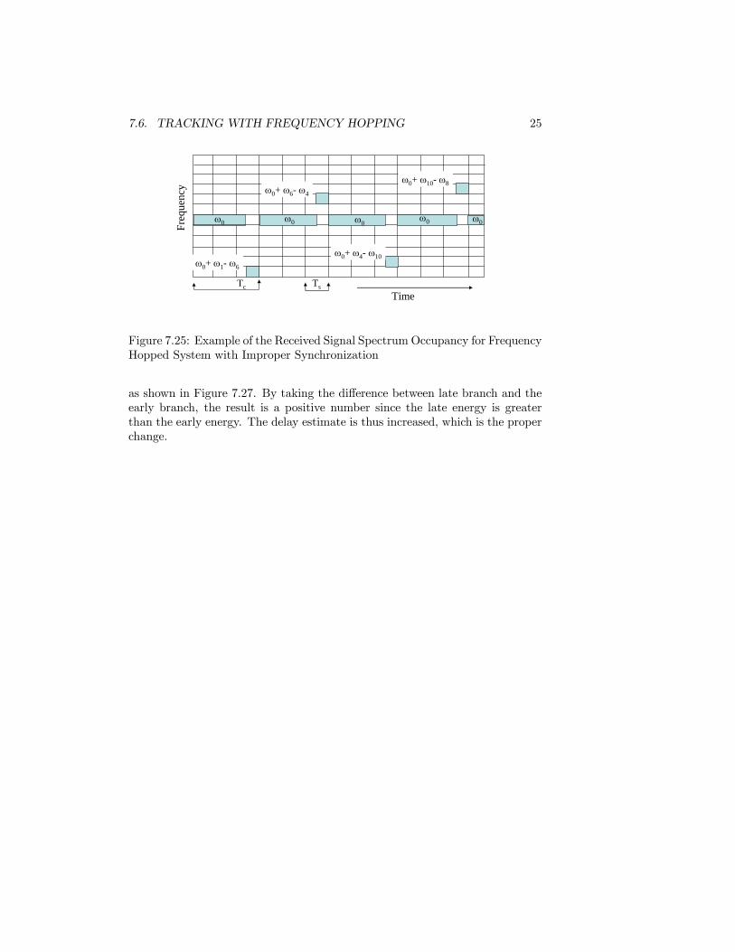
7.6. TRACKING WITH FREQUENCY HOPPING 25
Tc Ts
ω0
Time
Freq
uenc
y
ω0 ω0ω0 ω0
ω0+ ω1- ω6
ω0+ ω6- ω4
ω0+ ω4- ω10
ω0+ ω10- ω8
Figure 7.25: Example of the Received Signal Spectrum Occupancy for FrequencyHopped System with Improper Synchronization
as shown in Figure 7.27. By taking the difference between late branch and theearly branch, the result is a positive number since the late energy is greaterthan the early energy. The delay estimate is thus increased, which is the properchange.
26 CHAPTER 7. TRACKING OF SPREAD SPECTRUM SIGNALS
Tc Ts
ω0
Time
Freq
uenc
y
ω0 ω0 ω0 ω0
ω0+ ω1- ω6
ω0+ ω6- ω4
ω0+ ω4- ω10
ω0+ ω10- ω8
BPF captures only this band
Figure 7.26: Example of the Received Signal Spectrum Occupancy for EarlyBranch of Frequency Hopped Tracking Loop
Tc Ts
ω0
Time
Freq
uenc
y
ω0 ω0ω0
ω0+ ω1- ω3
ω0+ ω6- ω1
ω0+ ω4- ω6
ω0+ ω10- ω4
ω0+ ω8- ω10
BPF captures only this band
Figure 7.27: Example of the Received Signal Spectrum Occupancy for EarlyBranch of Frequency Hopped Tracking Loop

Bibliography
[1] T. I. Standard-95, “Mobile station-base station compatibility standard fordual-mode wideband spread spectrum cellular systems,” July 1993.
[2] R. Peterson, R. Ziemer, and D. Borth, Introduction to Spread SpectrumCommunications. Prentice-Hall, 1995.
27