Embed Size (px)
Citation preview

Training Manual
Course: C31P15
Direct View/ProjectionTelevision TroubleshootingDA-4 & DA-4X Chassis
Models: DA-4 DA-4XKV-32HS500 KP-57WV600KV-32HV600 KP-57WV700KV-34XBR800 KP-65WV600KV-36HS500 KP-65WV700KV-36XBR800KV-40XBR800
Theory of Operation & Practical Troubleshooting Tips
KV-36HV500
KV-57WV700
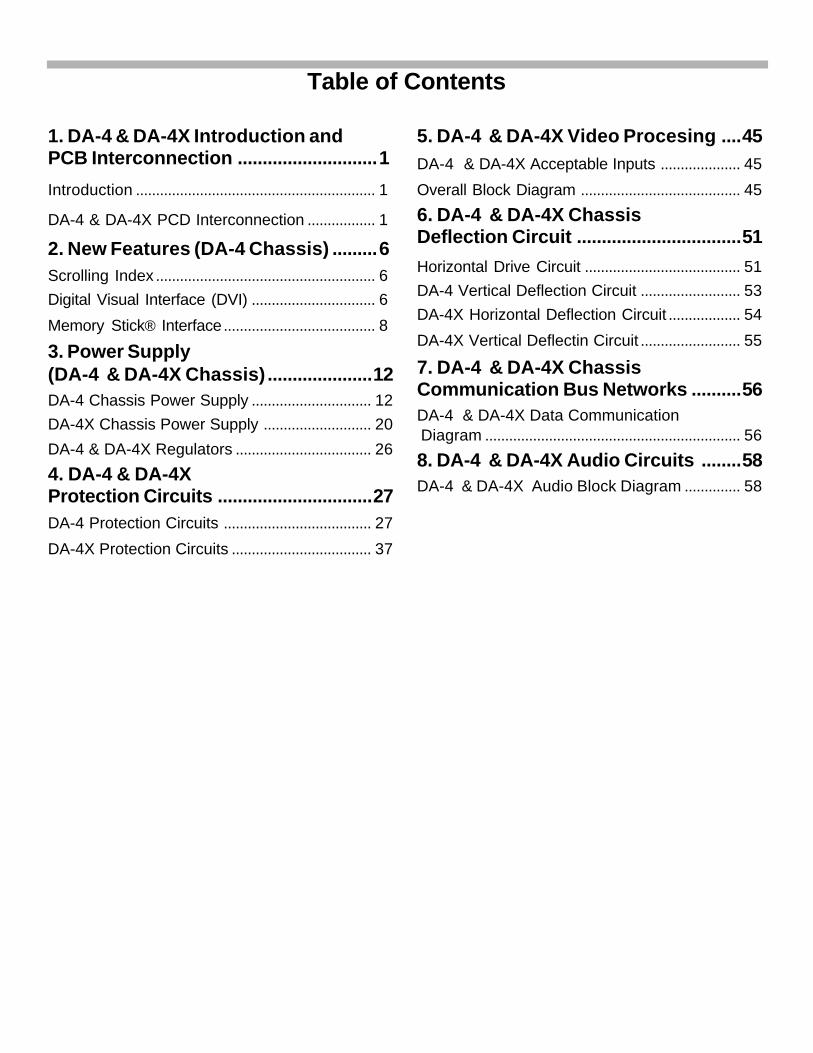
Table of Contents
1. DA-4 & DA-4X Introduction andPCB Interconnection ............................1
Introduction ............................................................ 1
DA-4 & DA-4X PCD Interconnection ................. 1
2. New Features (DA-4 Chassis) .........6Scrolling Index ....................................................... 6Digital Visual Interface (DVI) ............................... 6
Memory Stick® Interface...................................... 8
3. Power Supply(DA-4 & DA-4X Chassis) .....................12DA-4 Chassis Power Supply .............................. 12DA-4X Chassis Power Supply ........................... 20
DA-4 & DA-4X Regulators .................................. 26
4. DA-4 & DA-4XProtection Circuits ...............................27DA-4 Protection Circuits ..................................... 27
DA-4X Protection Circuits ................................... 37
5. DA-4 & DA-4X Video Procesing ....45DA-4 & DA-4X Acceptable Inputs .................... 45
Overall Block Diagram ........................................ 45
6. DA-4 & DA-4X ChassisDeflection Circuit .................................51
Horizontal Drive Circuit ....................................... 51DA-4 Vertical Deflection Circuit ......................... 53DA-4X Horizontal Deflection Circuit .................. 54
DA-4X Vertical Deflectin Circuit ......................... 55
7. DA-4 & DA-4X ChassisCommunication Bus Networks ..........56DA-4 & DA-4X Data Communication Diagram ................................................................ 56
8. DA-4 & DA-4X Audio Circuits ........58DA-4 & DA-4X Audio Block Diagram .............. 58
1
1. Introduction and DA-4 & DA-4X PCB Interconnection
Chapter 1 - Introduction andDA-4 & DA-4X PCB Interconnection
IntroductionOverviewThe C31P15 course covers the DA-4 (Direct View) and the DA-4X (Projection) chassis. The content includesnew features such as Memory Stick and DVI. Also included is theory of operation and troubleshooting tips for allmajor circuits (Power Supplies, Protection, Deflection, Communications and Audio) in the DA-4 and DA-X chassis.This training manual is based on the KV-32HV600 model.
Objectives
• New Features
• Circuit Theory of Operation
• Component and Board level troubleshooting
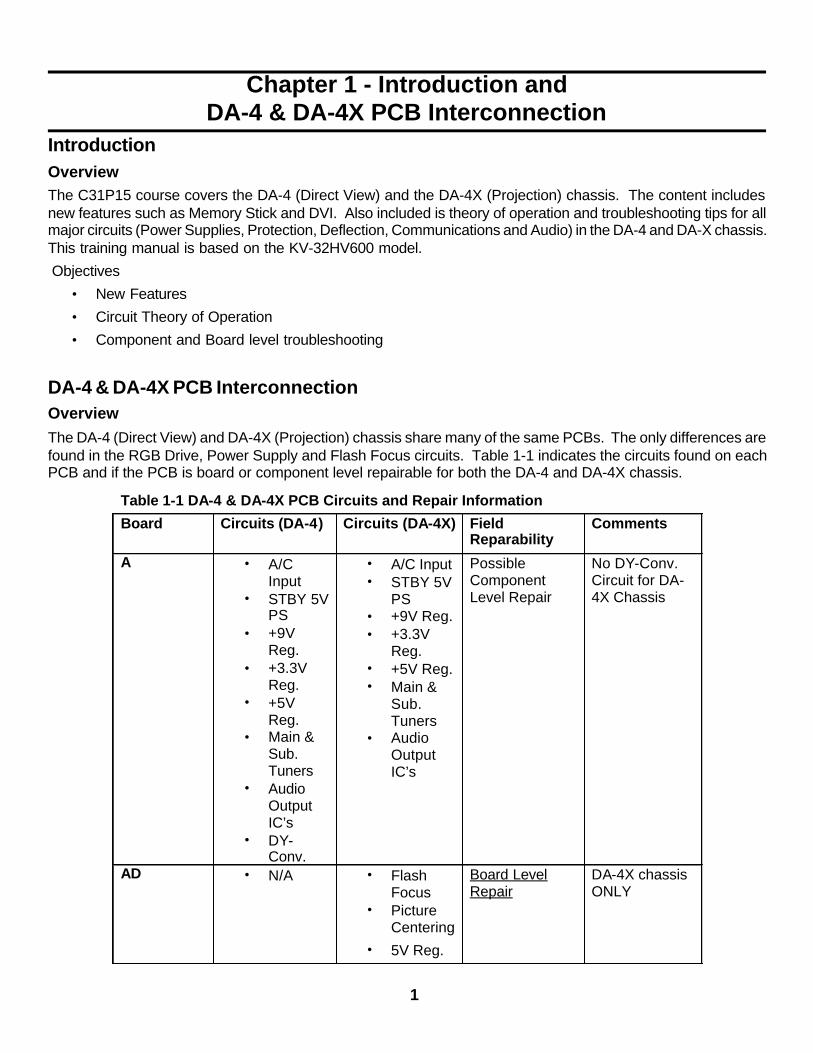
DA-4 & DA-4X PCB InterconnectionOverviewThe DA-4 (Direct View) and DA-4X (Projection) chassis share many of the same PCBs. The only differences arefound in the RGB Drive, Power Supply and Flash Focus circuits. Table 1-1 indicates the circuits found on eachPCB and if the PCB is board or component level repairable for both the DA-4 and DA-4X chassis.
Table 1-1 DA-4 & DA-4X PCB Circuits and Repair Information
Board Circuits (DA-4) Circuits (DA-4X) Field Reparability
Comments
A • A/C Input
• STBY 5V PS
• +9V Reg.
• +3.3V Reg.
• +5V Reg.
• Main & Sub. Tuners
• Audio Output IC’s
• DY-Conv.
• A/C Input • STBY 5V
PS • +9V Reg. • +3.3V
Reg. • +5V Reg. • Main &
Sub. Tuners
• Audio Output IC’s
Possible Component Level Repair
No DY-Conv. Circuit for DA-4X Chassis
AD • N/A • Flash Focus
• Picture Centering
• 5V Reg.
Board Level Repair
DA-4X chassis ONLY
2
1. Introduction and DA-4 & DA-4X PCB Interconnection
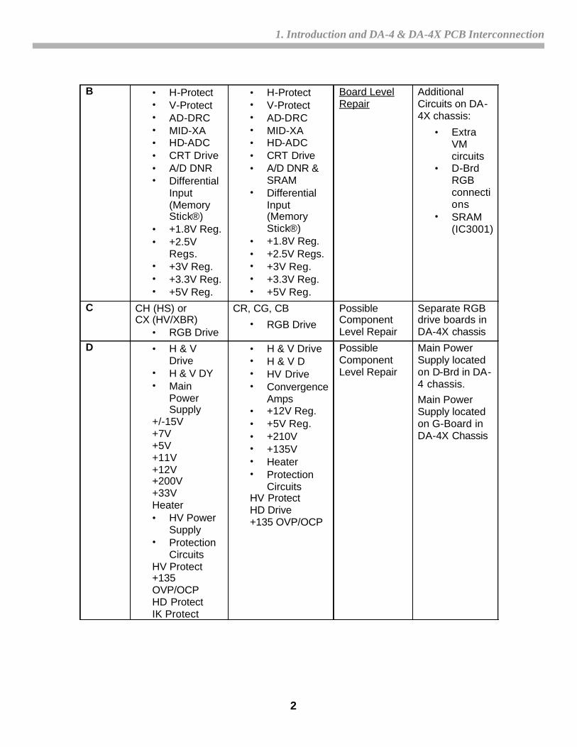
B • H-Protect • V-Protect • AD-DRC • MID-XA • HD-ADC • CRT Drive • A/D DNR • Differential
Input (Memory Stick®)
• +1.8V Reg. • +2.5V
Regs. • +3V Reg. • +3.3V Reg. • +5V Reg.
• H-Protect • V-Protect • AD-DRC • MID-XA • HD-ADC • CRT Drive • A/D DNR &
SRAM • Differential
Input (Memory Stick®)
• +1.8V Reg. • +2.5V Regs. • +3V Reg. • +3.3V Reg. • +5V Reg.
Board Level Repair
Additional Circuits on DA-4X chassis:
• Extra VM circuits
• D-Brd RGB connections
• SRAM (IC3001)
C CH (HS) or CX (HV/XBR)
• RGB Drive
CR, CG, CB • RGB Drive
Possible Component Level Repair
Separate RGB drive boards in DA-4X chassis
D • H & V Drive
• H & V DY • Main
Power Supply
+/-15V +7V +5V +11V +12V +200V +33V Heater • HV Power
Supply • Protection
Circuits HV Protect +135 OVP/OCP HD Protect IK Protect
• H & V Drive • H & V D • HV Drive • Convergence
Amps • +12V Reg. • +5V Reg. • +210V • +135V • Heater • Protection
Circuits HV Protect HD Drive +135 OVP/OCP
Possible Component Level Repair
Main Power Supply located on D-Brd in DA-4 chassis. Main Power Supply located on G-Board in DA-4X Chassis
3
1. Introduction and DA-4 & DA-4X PCB Interconnection
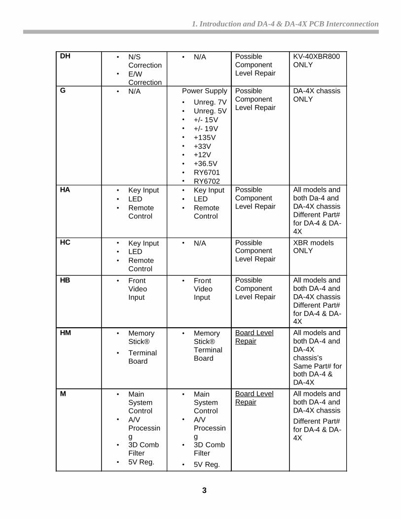
DH • N/S Correction
• E/W Correction
• N/A Possible Component Level Repair
KV-40XBR800 ONLY
G • N/A Power Supply
• Unreg. 7V • Unreg. 5V • +/- 15V • +/- 19V • +135V • +33V • +12V • +36.5V • RY6701 • RY6702
Possible Component Level Repair
DA-4X chassis ONLY
HA • Key Input • LED • Remote
Control
• Key Input • LED • Remote
Control
Possible Component Level Repair
All models and both Da-4 and DA-4X chassis Different Part# for DA-4 & DA-4X
HC • Key Input • LED • Remote
Control
• N/A Possible Component Level Repair
XBR models ONLY
HB • Front Video Input
• Front Video Input
Possible Component Level Repair
All models and both DA-4 and DA-4X chassis Different Part# for DA-4 & DA-4X
HM • Memory Stick®
• Terminal Board
• Memory Stick® Terminal Board
Board Level Repair
All models and both DA-4 and DA-4X chassis’s Same Part# for both DA-4 & DA-4X
M • Main System Control
• A/V Processing
• 3D Comb Filter
• 5V Reg.
• Main System Control
• A/V Processing
• 3D Comb Filter
• 5V Reg.
Board Level Repair
All models and both DA-4 and DA-4X chassis Different Part# for DA-4 & DA-4X
4
1. Introduction and DA-4 & DA-4X PCB Interconnection
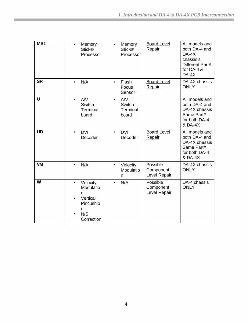
MS1 • Memory Stick® Processor
• Memory Stick® Processor
Board Level Repair
All models and both DA-4 and DA-4X chassis’s Different Part# for DA-4 & DA-4X
SR • N/A • Flash Focus Sensor
Board Level Repair
DA-4X chassis ONLY
U • A/V Switch Terminal board
• A/V Switch Terminal board
All models and both DA-4 and DA-4X chassis Same Part# for both DA-4 & DA-4X
UD • DVI Decoder
• DVI Decoder
Board Level Repair
All models and both DA-4 and DA-4X chassis Same Part# for both DA-4 & DA-4X
VM • N/A • Velocity Modulation
Possible Component Level Repair
DA-4X chassis ONLY
W • Velocity Modulation
• Vertical Pincushion
• N/S Correction
• N/A Possible Component Level Repair
DA-4 chassis ONLY
5
1. Introduction and DA-4 & DA-4X PCB Interconnection
MAIN MICRO3D COMBVIDEO PROCESSORAUDIO PROCESSORCCD,V-CHIP,ID1
KEYSSIRCSLED
MAIN MICRO3D COMBVIDEO PROCESSORAUDIO PROCESSORCCD,V-CHIP,ID1
HA/HC (XBR)
DVI
UD
M
A/V INPUTS(1-7)
AUDIO OUTMONITOR
OUTS-CONTROL
A/VSWITCH
U
HB
FRONTA/V INPUT
AC/DC POWERAUDIO POWERTUNERDY CONV.,(DA-4)
A
DGC
SPEAKERSDY
CONVERTER
ANTENNASWITCH
POWERSUPPLY
ACINPUT
H/V DRIVEH/V DYPOWER SUPPLYAC RECT.DEFLECTION
G
AD DRCMID - XAHD - ADCCRT DRIVEAD DNR
B
DA-4XCHASSIS
VELOCITYMOD
VM
MS 1
MEMORYSTICK PROCESSOR
D
VELOCITYMOD.V - PINN/S DRIVE
W
HM
MEMORYSTICKINTERFACE
CH/CX(XBR)
VIDEO OUT
MEMORYSTICK
N/S COILV-PIN COIL
QP COIL
VIDEOOUT
CR
VIDEOOUT
CG
VIDEOOUT
CB
DA-4XCHASSIS
DA-4CHASSIS
LANDINGCORRECTION
DH
KV40XBR 800 ONLY
DA-4XCHASSIS
HORIZONTAL &VERTICAL
DEFLECTION YOKE CRT
CRT
CRT
CRT
DVI MOLEXCONNECTOR
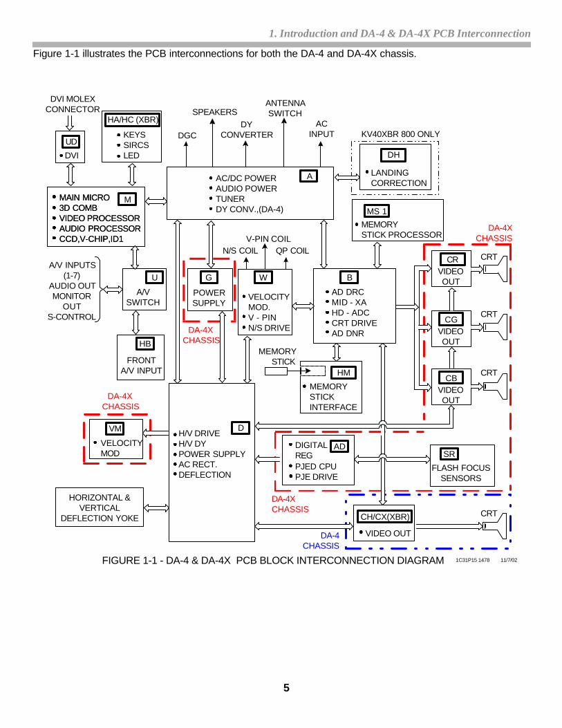
FIGURE 1-1 - DA-4 & DA-4X PCB BLOCK INTERCONNECTION DIAGRAM
SR
FLASH FOCUSSENSORS
DIGITALREGPJED CPUPJE DRIVE
AD
DA-4XCHASSIS
1C31P15 1478 11/7/02
Figure 1-1 illustrates the PCB interconnections for both the DA-4 and DA-4X chassis.
6
2. New Features (DA-4 Chassis)
Chapter 2 - New Features (DA-4 & DA-4X Chassis)
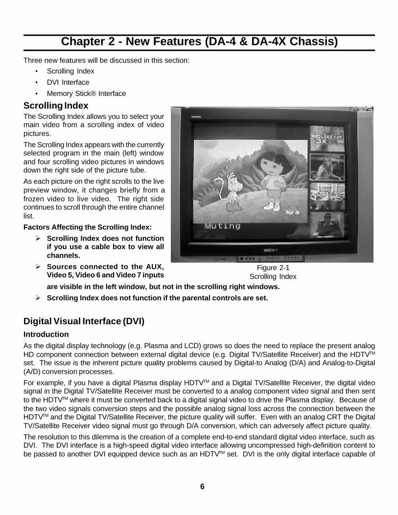
Figure 2-1Scrolling Index
Three new features will be discussed in this section:• Scrolling Index
• DVI Interface
• Memory Stick® Interface
Scrolling IndexThe Scrolling Index allows you to select yourmain video from a scrolling index of videopictures.
The Scrolling Index appears with the currentlyselected program in the main (left) windowand four scrolling video pictures in windowsdown the right side of the picture tube.
As each picture on the right scrolls to the livepreview window, it changes briefly from afrozen video to live video. The right sidecontinues to scroll through the entire channellist.
Factors Affecting the Scrolling Index:
Ø Scrolling Index does not functionif you use a cable box to view allchannels.
Ø Sources connected to the AUX,Video 5, Video 6 and Video 7 inputs
are visible in the left window, but not in the scrolling right windows.
Ø Scrolling Index does not function if the parental controls are set.
Digital Visual Interface (DVI)IntroductionAs the digital display technology (e.g. Plasma and LCD) grows so does the need to replace the present analogHD component connection between external digital device (e.g. Digital TV/Satellite Receiver) and the HDTVTM
set. The issue is the inherent picture quality problems caused by Digital-to Analog (D/A) and Analog-to-Digital(A/D) conversion processes.
For example, if you have a digital Plasma display HDTVTM and a Digital TV/Satellite Receiver, the digital videosignal in the Digital TV/Satellite Receiver must be converted to a analog component video signal and then sentto the HDTVTM where it must be converted back to a digital signal video to drive the Plasma display. Because ofthe two video signals conversion steps and the possible analog signal loss across the connection between theHDTVTM and the Digital TV/Satellite Receiver, the picture quality will suffer. Even with an analog CRT the DigitalTV/Satellite Receiver video signal must go through D/A conversion, which can adversely affect picture quality.
The resolution to this dilemma is the creation of a complete end-to-end standard digital video interface, such asDVI. The DVI interface is a high-speed digital video interface allowing uncompressed high-definition content tobe passed to another DVI equipped device such as an HDTVTM set. DVI is the only digital interface capable of
7
2. New Features (DA-4 Chassis)
1 2 9 1 0 1 7 1 8 2 3 2 4 6 7 1 4 1 6
I C 7 0 0 4D V I - D E C O D E R
9 4
9 5
R 7 0 2 11 0 k H z
5 V T OD 7 0 0 1
C N 7 0 0 12 4 P M O L E XC O N N E C T O R
R x 2 -R x 2 +
R x 1 -R x 1+
R x 0 - R x C +R x C -
S C LS D A
5VH P D
I C 7 0 0 1N V M
R x 0 +
3 . 3 VR E G
2 . 5 VR E G
I C 7 0 0 5M C U I C 7 0 0 6
N V M
2
3
3.3V
2 . 5 V
5V
5V
5V
3 . 3 V 2 . 5 V
5V
C N 7 0 0 2
S D A , S C L
S D A ,S C L
X 7 0 0 11 4 . 3 1 8 1 8 M H z
X 7 0 0 21 2 M H z
1 0
8
6
1 343
2
15 V
Y
P BP R
S E T - U P
M U T E
V G A
R E S E T5V
F I G U R E 2 - 2 - U D - B O A R D B L O C K ( D V I D E C O D E R )C 3 1 P 1 5 - 2 - 2 1 5 0 1 1 0 / 3 1 / 0 2
C N 2 3 0 4 /P I N 15V
C O N N E C T O R
accommodating uncompressed digital data such as HD video. DVI also has the bandwidth to support higheraudio fidelity.
DVI has a bandwidth of up to 5 Gigabits/sec, which is more then enough to accommodate an uncompressed HDvideo transmission that typically requires 2.2 Gigabits/sec bandwidth.
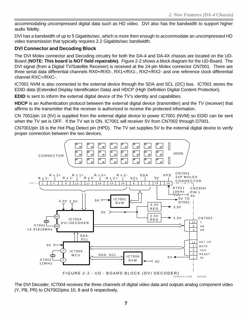
DVI Connector and Decoding BlockThe DVI Molex connector and Decoding circuitry for both the DA-4 and DA-4X chassis are located on the UD-Board (NOTE: This board is NOT field repairable). Figure 2-2 shows a block diagram for the UD-Board. TheDVI signal (from a Digital TV/Satellite Receiver) is received at the 24-pin Molex connector CN7001. There arethree serial data differential channels RX0+/RX0-, RX1+/RX1-, RX2+/RX2- and one reference clock differentialchannel RXC+/RXC-.
IC7001 NVM is also connected to the external device through the SDA and SCL (I2C) bus. IC7001 stores theEDID data (Extended Display Identification Data) and HDCP (High Definition Digital Content Protection).EDID is sent to inform the external digital device of the TV’s identity and capabilities.
HDCP is an Authentication protocol between the external digital device (transmitter) and the TV (receiver) thataffirms to the transmitter that the receiver is authorized to receive the protected information.
CN 7001/pin 14 (5V) is supplied from the external digital device to power IC7001 (NVM) so EDID can be sentwhen the TV set is OFF. If the TV set is ON, IC7001 will receiver 5V from CN7002 through D7001.CN7001/pin 16 is the Hot Plug Detect pin (HPD). The TV set supplies 5V to the external digital device to verifyproper connection between the two devices.
The DVI Decoder, IC7004 receives the three channels of digital video data and outputs analog component video(Y, PB, PR) to CN7002/pins 10, 8 and 6 respectively.
8
2. New Features (DA-4 Chassis)
DSC0001
DSC0002
DSC0003
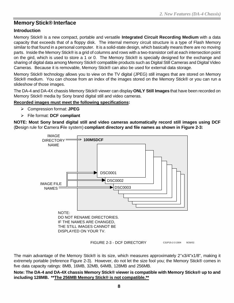
100MSDCFIMAGE
DIRECTORYNAME
IMAGE FILENAMES
FIGURE 2-3 - DCF DIRECTORY C31P15-2-3 1504 9/26/02
NOTE:DO NOT RENAME DIRECTORIES.IF THE NAMES ARE CHANGED,THE STILL IMAGES CANNOT BEDISPLAYED ON YOUR TV.
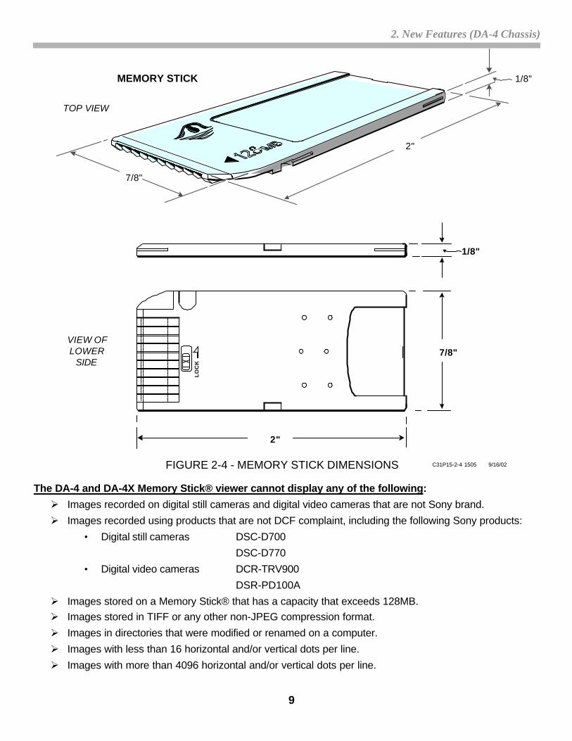
Memory Stick® InterfaceIntroductionMemory Stick® is a new compact, portable and versatile Integrated Circuit Recording Medium with a datacapacity that exceeds that of a floppy disk. The internal memory circuit structure is a type of Flash Memorysimilar to that found in a personal computer. It is a solid-state design, which basically means there are no movingparts. Inside the Memory Stick® is a grid of columns and rows with a two-transistor cell at each intersection pointon the gird, which is used to store a 1 or 0. The Memory Stick® is specially designed for the exchange andsharing of digital data among Memory Stick® compatible products such as Digital Still Cameras and Digital VideoCameras. Because it is removable, Memory Stick® can also be used for external data storage.
Memory Stick® technology allows you to view on the TV digital (JPEG) still images that are stored on MemoryStick® medium. You can choose from an index of the images stored on the Memory Stick® or you can run aslideshow of those images.
The DA-4 and DA-4X chassis Memory Stick® viewer can display ONLY Still Images that have been recorded onMemory Stick® media by Sony brand digital still and video cameras.Recorded images must meet the following specifications:
Ø Compression format: JPEG
Ø File format: DCF compliant
NOTE: Most Sony brand digital still and video cameras automatically record still images using DCF(Design rule for Camera File system) compliant directory and file names as shown in Figure 2-3:
The main advantage of the Memory Stick® is its size, which measures approximately 2’’x3/4"x1/8", making itextremely portable (reference Figure 2-3). However, do not let the size fool you; the Memory Stick® comes infive data capacity ratings: 8MB, 16MB, 32MB, 64MB, 128MB and 256MB.Note: The DA-4 and DA-4X chassis Memory Stick® viewer is compatible with Memory Sticks® up to andincluding 128MB. **The 256MB Memory Stick® is not compatible.**
9
2. New Features (DA-4 Chassis)
7/8"
2"
1/8"
LOC
K
1/8"
7/8"
2"
MEMORY STICK
FIGURE 2-4 - MEMORY STICK DIMENSIONS
VIEW OFLOWER
SIDE
TOP VIEW
C31P15-2-4 1505 9/16/02
The DA-4 and DA-4X Memory Stick® viewer cannot display any of the following:
Ø Images recorded on digital still cameras and digital video cameras that are not Sony brand.
Ø Images recorded using products that are not DCF complaint, including the following Sony products:
• Digital still cameras DSC-D700
DSC-D770
• Digital video cameras DCR-TRV900
DSR-PD100A
Ø Images stored on a Memory Stick® that has a capacity that exceeds 128MB.Ø Images stored in TIFF or any other non-JPEG compression format.
Ø Images in directories that were modified or renamed on a computer.
Ø Images with less than 16 horizontal and/or vertical dots per line.
Ø Images with more than 4096 horizontal and/or vertical dots per line.
10
2. New Features (DA-4 Chassis)
3 5 6 7 8 9 10 11 12 13 14 15
MS-SDI+ MS-INSMS-SDIMS-SDO-
MS-SDO+MS-SCLK+MS-SCLK-MS-DIR-
MS-DIR+MS-BS-
MS-BS+3.3V
B3 A4 BY A5 B5 A6 B6 A7 B7 A8 B8 B9
DIFF. - AMPS& BUFFER MID
CN7201
CN7202
CN3601
CN104
CN3603
TO CRTDRIVE
MEMORYSTICK
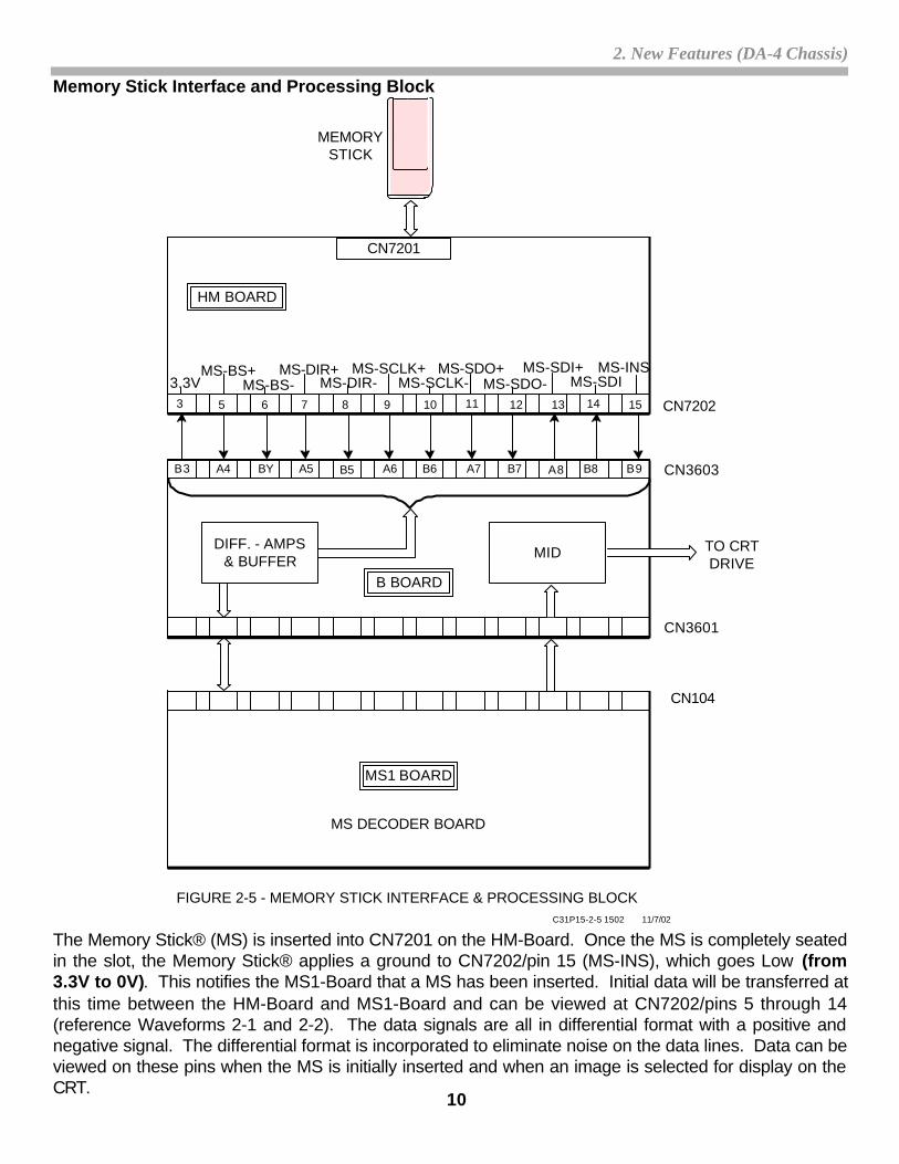
FIGURE 2-5 - MEMORY STICK INTERFACE & PROCESSING BLOCK
MS DECODER BOARD
C31P15-2-5 1502 11/7/02
B BOARD
MS1 BOARD
HM BOARD
Memory Stick Interface and Processing Block
The Memory Stick® (MS) is inserted into CN7201 on the HM-Board. Once the MS is completely seatedin the slot, the Memory Stick® applies a ground to CN7202/pin 15 (MS-INS), which goes Low (from3.3V to 0V). This notifies the MS1-Board that a MS has been inserted. Initial data will be transferred atthis time between the HM-Board and MS1-Board and can be viewed at CN7202/pins 5 through 14(reference Waveforms 2-1 and 2-2). The data signals are all in differential format with a positive andnegative signal. The differential format is incorporated to eliminate noise on the data lines. Data can beviewed on these pins when the MS is initially inserted and when an image is selected for display on theCRT.
11
2. New Features (DA-4 Chassis)
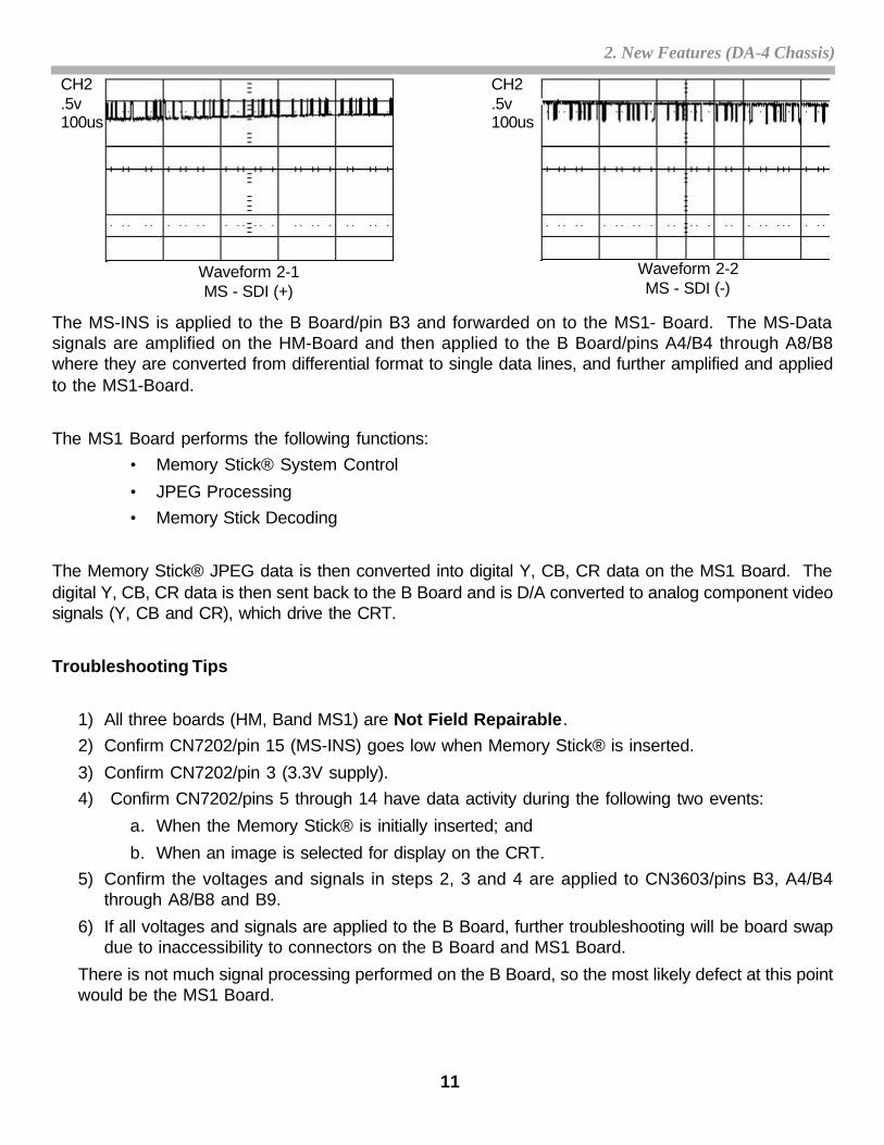
Waveform 2-1MS - SDI (+)
CH2.5v100us
Waveform 2-2MS - SDI (-)
CH2.5v100us
The MS-INS is applied to the B Board/pin B3 and forwarded on to the MS1- Board. The MS-Datasignals are amplified on the HM-Board and then applied to the B Board/pins A4/B4 through A8/B8where they are converted from differential format to single data lines, and further amplified and appliedto the MS1-Board.
The MS1 Board performs the following functions:• Memory Stick® System Control
• JPEG Processing• Memory Stick Decoding
The Memory Stick® JPEG data is then converted into digital Y, CB, CR data on the MS1 Board. Thedigital Y, CB, CR data is then sent back to the B Board and is D/A converted to analog component videosignals (Y, CB and CR), which drive the CRT.
Troubleshooting Tips
1) All three boards (HM, Band MS1) are Not Field Repairable.2) Confirm CN7202/pin 15 (MS-INS) goes low when Memory Stick® is inserted.
3) Confirm CN7202/pin 3 (3.3V supply).4) Confirm CN7202/pins 5 through 14 have data activity during the following two events:
a. When the Memory Stick® is initially inserted; and
b. When an image is selected for display on the CRT.5) Confirm the voltages and signals in steps 2, 3 and 4 are applied to CN3603/pins B3, A4/B4
through A8/B8 and B9.
6) If all voltages and signals are applied to the B Board, further troubleshooting will be board swapdue to inaccessibility to connectors on the B Board and MS1 Board.
There is not much signal processing performed on the B Board, so the most likely defect at this pointwould be the MS1 Board.
12
3. Power Supply (DA-4 & DA-4X Chassis)
Chapter 3 - Power Supply (DA-4 & DA-4X Chassis)
STANDBY 5VPOWERSUPPLY
D501
1 2
IC6501MAIN
POWERSUPPLY
RY6502
IC8002HV POWER
SUPPLY
R6516
GND.FROMQ6527
FROMUNREG
11V
STANDBY5V CIRCUIT
HA/HE BD.
M BD.
+/- 15VUNREG 7V
UNREG 5V
UNREG 11V+135V+200V
D503/C506
AC
FROM AC RECT.BLOCK D6530
VD501
FH501
T510 T511
RY501
13V FROM 5V STBY
R506C507
+Q502 DGC-ON
FROMIC2300/PIN 68( M-BD.)
Q501
CN514
CN6502
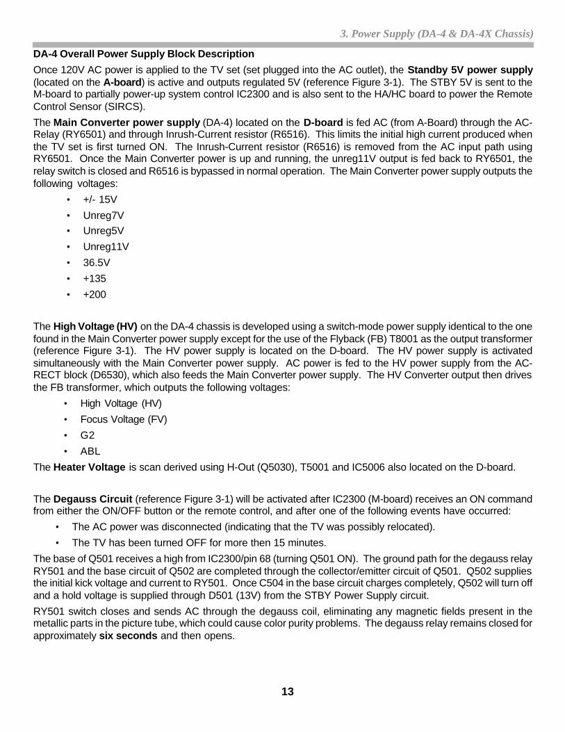
FIGURE 3-1 - DA-4 POWER SUPPLY OVERALL BLOCK C31P15-3-1 1509 10/28/02
A BOARD
D BOARD
TH501
36.5V
DGC
H1( HEATER)
HVG2FVABLDF
IC5006
FROM D508,D509
T8001FBT
H-OUTQ5030
HOTT5001
RY6501
(ACRELAY)
(INRUSHRELAY)
AC-RECT
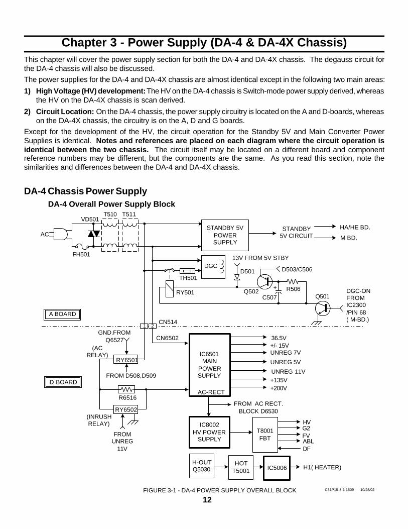
This chapter will cover the power supply section for both the DA-4 and DA-4X chassis. The degauss circuit forthe DA-4 chassis will also be discussed.The power supplies for the DA-4 and DA-4X chassis are almost identical except in the following two main areas:
1) High Voltage (HV) development: The HV on the DA-4 chassis is Switch-mode power supply derived, whereasthe HV on the DA-4X chassis is scan derived.
2) Circuit Location: On the DA-4 chassis, the power supply circuitry is located on the A and D-boards, whereason the DA-4X chassis, the circuitry is on the A, D and G boards.
Except for the development of the HV, the circuit operation for the Standby 5V and Main Converter PowerSupplies is identical. Notes and references are placed on each diagram where the circuit operation isidentical between the two chassis. The circuit itself may be located on a different board and componentreference numbers may be different, but the components are the same. As you read this section, note thesimilarities and differences between the DA-4 and DA-4X chassis.
DA-4 Chassis Power SupplyDA-4 Overall Power Supply Block
13
3. Power Supply (DA-4 & DA-4X Chassis)
DA-4 Overall Power Supply Block Description
Once 120V AC power is applied to the TV set (set plugged into the AC outlet), the Standby 5V power supply(located on the A-board) is active and outputs regulated 5V (reference Figure 3-1). The STBY 5V is sent to theM-board to partially power-up system control IC2300 and is also sent to the HA/HC board to power the RemoteControl Sensor (SIRCS).
The Main Converter power supply (DA-4) located on the D-board is fed AC (from A-Board) through the AC-Relay (RY6501) and through Inrush-Current resistor (R6516). This limits the initial high current produced whenthe TV set is first turned ON. The Inrush-Current resistor (R6516) is removed from the AC input path usingRY6501. Once the Main Converter power is up and running, the unreg11V output is fed back to RY6501, therelay switch is closed and R6516 is bypassed in normal operation. The Main Converter power supply outputs thefollowing voltages:
• +/- 15V
• Unreg7V• Unreg5V
• Unreg11V
• 36.5V
• +135
• +200
The High Voltage (HV) on the DA-4 chassis is developed using a switch-mode power supply identical to the onefound in the Main Converter power supply except for the use of the Flyback (FB) T8001 as the output transformer(reference Figure 3-1). The HV power supply is located on the D-board. The HV power supply is activatedsimultaneously with the Main Converter power supply. AC power is fed to the HV power supply from the AC-RECT block (D6530), which also feeds the Main Converter power supply. The HV Converter output then drivesthe FB transformer, which outputs the following voltages:
• High Voltage (HV)
• Focus Voltage (FV)
• G2
• ABL
The Heater Voltage is scan derived using H-Out (Q5030), T5001 and IC5006 also located on the D-board.
The Degauss Circuit (reference Figure 3-1) will be activated after IC2300 (M-board) receives an ON commandfrom either the ON/OFF button or the remote control, and after one of the following events have occurred:
• The AC power was disconnected (indicating that the TV was possibly relocated).
• The TV has been turned OFF for more then 15 minutes.
The base of Q501 receives a high from IC2300/pin 68 (turning Q501 ON). The ground path for the degauss relayRY501 and the base circuit of Q502 are completed through the collector/emitter circuit of Q501. Q502 suppliesthe initial kick voltage and current to RY501. Once C504 in the base circuit charges completely, Q502 will turn offand a hold voltage is supplied through D501 (13V) from the STBY Power Supply circuit.
RY501 switch closes and sends AC through the degauss coil, eliminating any magnetic fields present in themetallic parts in the picture tube, which could cause color purity problems. The degauss relay remains closed forapproximately six seconds and then opens.
14
3. Power Supply (DA-4 & DA-4X Chassis)
CN6502IC501STBY
5V
I O
G
77
IC2300
69
Q2312IC2300SYSCONIC2302 NVMIC2305 3.3VREG
HA/HCBD.
TO RY501DEGAUSS
RELAYSOLENOID
D501
D509
D508
Q503C506
D503
R516C513
L510
T502
FH501
CN523 CN900
CN5011
R6528
R6509
R6530
(AC)D6534
R6519
Q6527
C514
C515
AC RELAYRY6501
TO D6530MAIN POWER
SUPPLYR6516
D6533
RY6502(INRUSH)
RELAY
UNREG 11VOUTPUT FROMMAIN POWER
SUPPLY
5V
MBD.
+
+
+
NOTECIRCUIT OPERATION IS THE SAME FOR BOTH DA-4 & DA-4X CHASSIS
+
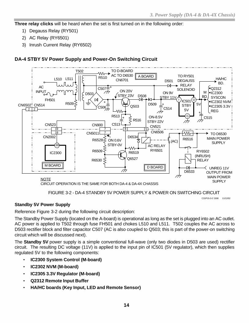
FIGURE 3-2 - DA-4 STANDBY 5V POWER SUPPLY & POWER ON SWITCHING CIRCUITC31P15-3-2 1508 11/12/02
M BOARD D BOARD
A BOARDL511
8 5
R513 ON-8.5VSTBY-22V
ON 20VSTBY 23V
TO D-BOARDAC TO D6530
CN6701
CN521
ON 0.6VSTBY-0V
CN514
ON 9VSTBY 11V
C507 +
22
ACINPUT
R509
R510
CN65061919
CN2002
Three relay clicks will be heard when the set is first turned on in the following order:
1) Degauss Relay (RY501)
2) AC Relay (RY6501)
3) Inrush Current Relay (RY6502)
DA-4 STBY 5V Power Supply and Power-On Switching Circuit
Standby 5V Power Supply
Reference Figure 3-2 during the following circuit description:
The Standby Power Supply (located on the A-board) is operational as long as the set is plugged into an AC outlet.AC power is applied to T502 through fuse FH501 and chokes L510 and L511. T502 couples the AC across toD503 rectifier block and filter capacitor C507 (AC is also coupled to Q503; this is part of the power-on switchingcircuit which will be discussed next).
The Standby 5V power supply is a simple conventional full-wave (only two diodes in D503 are used) rectifiercircuit. The resulting DC voltage (11V) is applied to the input pin of IC501 (5V regulator), which then suppliesregulated 5V to the following components:
• IC2300 System Control (M-board)
• IC2302 NVM (M-board)
• IC2305 3.3V Regulator (M-board)
• Q2312 Remote Input Buffer• HA/HC boards (Key Input, LED and Remote Sensor)
15
3. Power Supply (DA-4 & DA-4X Chassis)
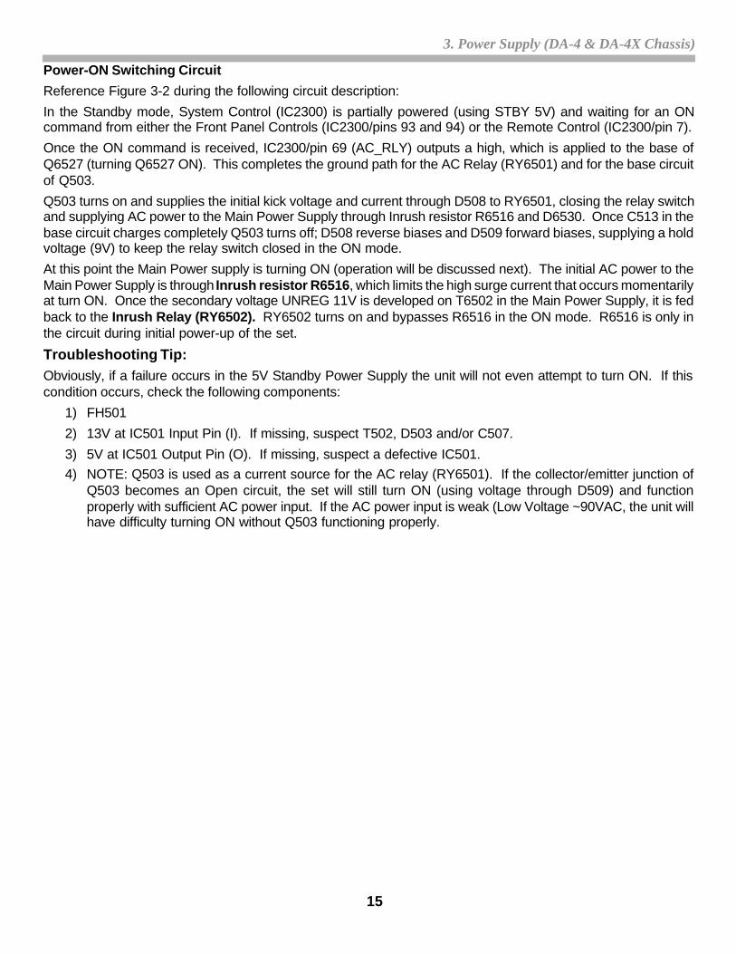
Power-ON Switching Circuit
Reference Figure 3-2 during the following circuit description:
In the Standby mode, System Control (IC2300) is partially powered (using STBY 5V) and waiting for an ONcommand from either the Front Panel Controls (IC2300/pins 93 and 94) or the Remote Control (IC2300/pin 7).
Once the ON command is received, IC2300/pin 69 (AC_RLY) outputs a high, which is applied to the base ofQ6527 (turning Q6527 ON). This completes the ground path for the AC Relay (RY6501) and for the base circuitof Q503.
Q503 turns on and supplies the initial kick voltage and current through D508 to RY6501, closing the relay switchand supplying AC power to the Main Power Supply through Inrush resistor R6516 and D6530. Once C513 in thebase circuit charges completely Q503 turns off; D508 reverse biases and D509 forward biases, supplying a holdvoltage (9V) to keep the relay switch closed in the ON mode.
At this point the Main Power supply is turning ON (operation will be discussed next). The initial AC power to theMain Power Supply is through Inrush resistor R6516, which limits the high surge current that occurs momentarilyat turn ON. Once the secondary voltage UNREG 11V is developed on T6502 in the Main Power Supply, it is fedback to the Inrush Relay (RY6502). RY6502 turns on and bypasses R6516 in the ON mode. R6516 is only inthe circuit during initial power-up of the set.
Troubleshooting Tip:Obviously, if a failure occurs in the 5V Standby Power Supply the unit will not even attempt to turn ON. If thiscondition occurs, check the following components:
1) FH501
2) 13V at IC501 Input Pin (I). If missing, suspect T502, D503 and/or C507.
3) 5V at IC501 Output Pin (O). If missing, suspect a defective IC501.4) NOTE: Q503 is used as a current source for the AC relay (RY6501). If the collector/emitter junction of
Q503 becomes an Open circuit, the set will still turn ON (using voltage through D509) and functionproperly with sufficient AC power input. If the AC power input is weak (Low Voltage ~90VAC, the unit willhave difficulty turning ON without Q503 functioning properly.
16
3. Power Supply (DA-4 & DA-4X Chassis)
FROMRY6501
CN6701
5 4
1
14
10
6
18
V-SENSE
VB
VC2
TIMER OCP
IC6501MCZ
3001D
16
15
712
VG(H)
VS
VG(L)
F/B VCI2 8
6
C6352R6557
R6556
9
FILTERCIRCUIT
1
2
2 1
C6546
+
4 1
3 2
18
17
16
15
14
13
8
9
11
10
IC6503DM-58CONT.
4 1
5
TO A BD.AUDIO VCC
(36.5V)
TO IC8002/PIN 1HV POWER SUPPLY
D6530AC RECT.
R6526
D6502
C6508+
C6519+
+C6558
TO IC8002/PIN 8
+
R6525
C6549
D6520
D6519
R6510
R6508
R6501
R6505
R6524
PH6502
+15VR6544
R6590
+
C6557D6518+200V
D6524
C6556
+
+135V
T6502PS6506
PS6505
D6513
D6516
+
+
UNREG11V
UNREG7V
UNREG 5V
+
+
+15V
-15V
D6523
CN6503
Q6507
Q6506
D-BOARD
NOTE:
CIRCUIT OPERATIONIS THE SAME FORBOTH DA4 & DA4XCHASSIS'
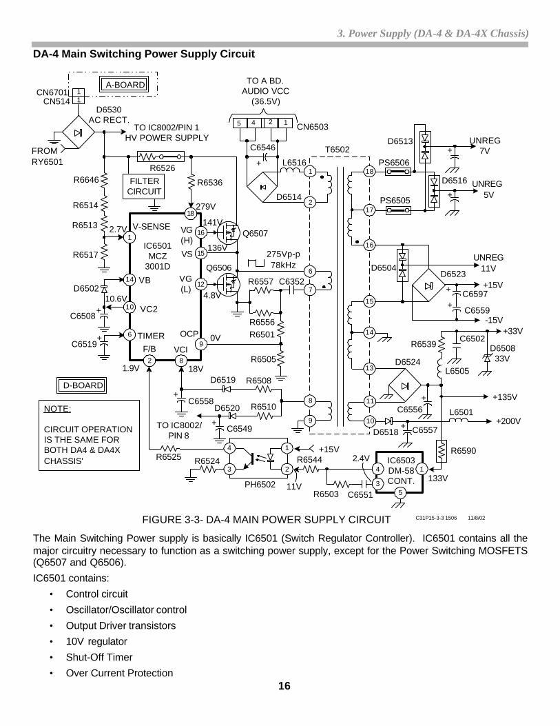
FIGURE 3-3- DA-4 MAIN POWER SUPPLY CIRCUIT C31P15-3-3 1506 11/8/02
11
CN514
A-BOARD
D6504
R6539
C6559
C659710.6V
2.7V
1.9V 18V
D6514
L6516
C6502
L6505
+33V
D650833V
133V
L6501
3
R6503 C6551
2.4V
0V
4.8V
141V
136V
R6646
R6514
R6513
R6517
279V
275Vp-p78kHz
11V
R6536
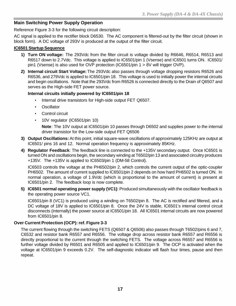
DA-4 Main Switching Power Supply Circuit
The Main Switching Power supply is basically IC6501 (Switch Regulator Controller). IC6501 contains all themajor circuitry necessary to function as a switching power supply, except for the Power Switching MOSFETS(Q6507 and Q6506).
IC6501 contains:
• Control circuit
• Oscillator/Oscillator control
• Output Driver transistors
• 10V regulator
• Shut-Off Timer
• Over Current Protection
17
3. Power Supply (DA-4 & DA-4X Chassis)
Main Switching Power Supply OperationReference Figure 3-3 for the following circuit description:AC signal is applied to the rectifier block D6530. The AC component is filtered-out by the filter circuit (shown inblock form). A DC voltage of 293V is produced at the output of the filter circuit.
IC6501 Startup Sequence
1) Turn ON voltage: The 293Vdc from the filter circuit is voltage divided by R6646, R6514, R6513 andR6517 down to 2.7Vdc. This voltage is applied to IC6501/pin 1 (Vsense) and IC6501 turns ON. IC6501/pin1 (Vsense) is also used for OVP protection (IC6501/pin 1 > 8V will trigger OVP).
2) Internal circuit Start Voltage: The 293Vdc also passes through voltage dropping resistors R6526 andR6536, and 279Vdc is applied to IC6501/pin 18. This voltage is used to initially power the internal circuitsand begin oscillations. Note that the 293Vdc from R6526 is connected directly to the Drain of Q6507 andserves as the High-side FET power source.
Internal circuits initially powered by IC6501/pin 18
• Internal drive transistors for High-side output FET Q6507.
• Oscillator
• Control circuit
• 10V regulator (IC6501/pin 10)Note: The 10V output at IC6501/pin 10 passes through D6502 and supplies power to the internaldriver transistor for the Low-side output FET Q6506
3) Output Oscillations: At this point, initial square-wave oscillations of approximately 125KHz are output atIC6501/ pins 16 and 12. Normal operation frequency is approximately 85KHz.
4) Regulator Feedback: The feedback line is connected to the +135V secondary output. Once IC6501 isturned ON and oscillations begin, the secondary winding at T6502/pin 13 and associated circuitry produces+135V. The +135V is applied to IC6503/pin 1 (DM-58 Control).
IC6503 controls the voltage at the PH6502/pin 2, which controls the current output of the optic-couplerPH6502. The amount of current supplied to IC6501/pin 2 depends on how hard PH6502 is turned ON. Innormal operation, a voltage of 1.9Vdc (which is proportional to the amount of current) is present atIC6501/pin 2. The feedback loop is now complete.
5) IC6501 normal operating power supply (VC1): Produced simultaneously with the oscillator feedback isthe operating power source VC1.
IC6501/pin 8 (VC1) is produced using a winding on T6502/pin 8. The AC is rectified and filtered, and aDC voltage of 18V is applied to IC6501/pin 8. Once the 24V is stable, IC6501’s internal control circuitdisconnects (internally) the power source at IC6501/pin 18. All IC6501 internal circuits are now poweredfrom IC6501/pin 8.
Over Current Protection (OCP): ref. Figure 3-3
The current flowing through the switching FETS (Q6507 & Q6506) also passes through T6502/pins 6 and 7,C6532 and resistor bank R6557 and R6556. The voltage drop across resistor bank R6557 and R6556 isdirectly proportional to the current through the switching FETS. The voltage across R6557 and R6556 isfurther voltage divided by R6501 and R6505 and applied to IC6501/pin 9. The OCP is activated when thevoltage at IC6501/pin 9 exceeds 0.2V. The self-diagnostic indicator will flash four times, pause and thenrepeat.
18
3. Power Supply (DA-4 & DA-4X Chassis)
Over Voltage Protection (OVP) and Under Voltage Protection (UVP): The voltage at IC6501/pin 8 (VC1) ismonitored by circuitry inside IC6501 for Under-voltage and Over-voltage conditions. The two conditions areas follows:
OVP – greater than 33V
UVP – less than 8V
If either of these two conditions occurs at IC6501/pin 8, the unit will go into protection mode. The self-diagnostic indicator will flash four times, pause and then repeat.
Troubleshooting Tips (ref. Figure 3-3)NOTE: Follow previously discussed “IC6501 Startup Sequence”. The five steps are in order of occurrence.
NOTE: Use HOT GRND when making measurements on primary side of T6502. This includes allmeasurements on IC6501.
Symptom: Unit goes into protection mode, LED flashes four times.
Check: This indicates either a Vertical deflection or power supply problem.
1) Check power supply secondary outputs.
• If voltages are present and at proper the level, then the problem is in the Vertical deflection drivecircuit.
• If the secondary voltages are low or missing, then the problem is in the power supply.
2) The power supply can be safely tested by unloading the +135v line. Unsolder R5013. This will unloadthe +135V line of the power supply, but still send necessary feedback to IC6501 for proper power supplyoperation.
3) If the power supply outputs proper secondary voltages after unsoldering R5013, suspect a shorted +135Vline
4) If the unit still goes into protection mode after unsoldering R5013, check the following items:
• D6538 (5V Zener) for shorted condition.
• Check IC6505 (B+ OVP) for proper operation.
• IC6501/pin 15 (this is midpoint for output MOSFETS Q6507 and Q6506). A 275Vpp, 85KHzsquare-wave should be present. If the waveform pulses four times and stops, check the nextItem.
• IC6501 Feedback circuit. The amount of current feedback can be determined by monitoring thevoltage drop across R6525. The minimum current feedback is 80uA, which is a minimum voltagedrop of 37.6mV. In normal operation, this voltage drop is approximately 223mV. If the voltagedrop is below 37.6mV, suspect components in the feedback path e.g. PH6502 and IC6503.Reference Figure 3-3 for proper voltages at these components.
• If no waveform is present when the unit is turned ON, then check IC6501/pins 1 and 18 for propervoltages (reference “IC6501 Startup Sequence” above).
If these voltages check OK, check IC6501/pin 8 for proper voltage of 24V. This is the voltageused to power IC6501 after initial startup.
If 18V is present at IC6501/pin8, check IC6501/pin 10 for 10.2V. This voltage is developed usingthe 18Vs and a voltage regulator circuit inside IC6501. If 10.2V is missing, suspect a defectiveIC6501. Also check voltage at IC6501/pin 14 (Use battery powered DVM for this measurementand use IC6501/pin 15 (VS) as ground ref.). The voltage at IC6501/pin 14 should be 10V. If thevoltage measured at IC6501/pin 14 is incorrect, check D618.
• If all the above measurements check OK, suspect a defective IC6501.
19
3. Power Supply (DA-4 & DA-4X Chassis)
1
14
10
6
18
V-SENSE
VB
VC2
TIMER OCP
IC8002MCZ
3001D
16
15
7
12
VG(H)
VS
VG(L)
F/B VCI2 8
9
9
4 1
3 2
HV
17
14
FV
6
5 1
IC8005CONTROL
1
2
R8051
D8010
C8025+
C8033+
R8065
R8059 PH8003
+15V
R8010
T8001
Q8014
Q8013
D-BOARD
FIGURE 3-4 - DA-4 HV POWER SUPPLY CIRCUIT
N/C
8 6
IC8004BUFFER
FROM MAIN POWERSUPPLY T6502/PIN 8
TO IC8001/PIN 5PROTECT.
DYNAMICFOCUS
FOCUS
R8085
R8096
R8072
C8037
R8070D8011
D8014
D8012
D8013
RV8002
R8017
R8015R8014
D800915V
FROM D6530AC-RECT.
C31P15-3-4 1507 11/8/02
13
D8015
D8030
- +
8
7
5
ABL
R8058
R8049
R8061
0V
4.8V
116V
111V
R8053
R80562.4V
121V
10.6V
R8054 R8055
L8002
D8022
10V
8.9V
1.9V 17V
7.4V
7.4V
7.4V
TOARCING
PROTECTIONCIRCUIT
32.4V
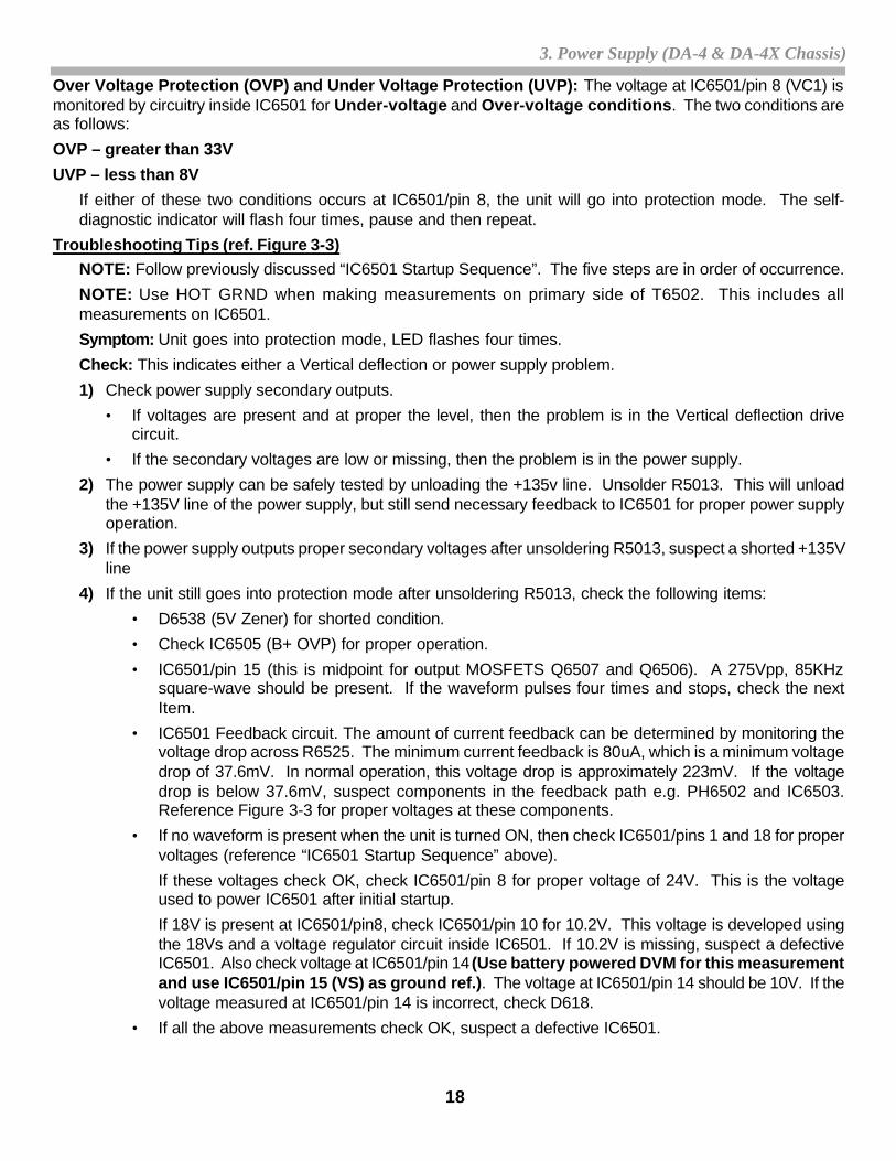
DA-4 High Voltage (HV) Power Supply Circuit
The HV Switching Power Supply uses the same switching IC as in the Main Power Supply (MCZ3001D).So, the theory of operation of IC8002 will be identical to that of IC6501 (reference IC6501 StartupSequence text for details) except for the following differences:
IC8002/pin 18 is not used because VC1 is supplied from the T6502/pin 8 in the Main Power Supplycircuit. Pin 18 is only needed when the switching IC (MCZ3001D) must supply its own VC1 through theoutput transformer.
20
3. Power Supply (DA-4 & DA-4X Chassis)
MAINPOWERSUPPLY
& RELAYS
UNREG 7V
UNREG 11V
UNREG 5V
12V
+/- 19V
+/- 15V
+36.5V
+135V
33V
STBY 5VPOWER SUPPLY STBY 5V A BOARD
G BOARD
FH501
VD501 T510 T511
H-OUTQ8043
T8004
T8005FBT
R8225
PS8007
210V
+/- H HEATER
HV
ABL
H-DRIVE
FIGURE 3-5 - DA-4X POWER SUPPLY OVERALL BLOCK 10/16/02C31P15-3-5
FV
FOCUSPACK
DF
G2
D BOARD
1 2
RY6701
RY6702
R6705
FROM Q6503
FROMIC6501
12V
CN514
CN6701
FROM D508,D509
(ACRELAY)
(INRUSHRELAY)
T8006Q8042Q8041
ACINPUT
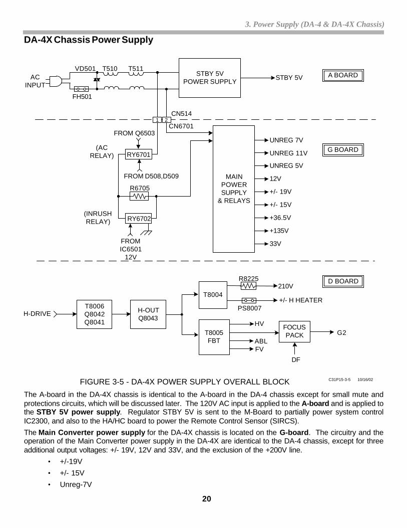
DA-4X Chassis Power Supply
The A-board in the DA-4X chassis is identical to the A-board in the DA-4 chassis except for small mute andprotections circuits, which will be discussed later. The 120V AC input is applied to the A-board and is applied tothe STBY 5V power supply. Regulator STBY 5V is sent to the M-Board to partially power system controlIC2300, and also to the HA/HC board to power the Remote Control Sensor (SIRCS).
The Main Converter power supply for the DA-4X chassis is located on the G-board. The circuitry and theoperation of the Main Converter power supply in the DA-4X are identical to the DA-4 chassis, except for threeadditional output voltages: +/- 19V, 12V and 33V, and the exclusion of the +200V line.
• +/-19V
• +/- 15V
• Unreg-7V
21
3. Power Supply (DA-4 & DA-4X Chassis)
IC501STANDBY
5V
I O
G
69
Q2312IC2300SYSCONIC2302 NVMIC2305 3.3VREG
HA/HCBD.
TO RY501DEGAUSS
RELAYSOLENOID
D509
D508
Q503C506
D503
R516C513
L510
T502
FH501
CN523 CN900CN6506CN2002
R6525
R6523
R6530
D6504
Q6503
C514
C515
RY6701(AC
RELAY)
TO D6702MAIN POWER
SUPPLYR6705
D6501
RY6702(INRUSH RELAY)
12VFROMIC6501
5V
MBD.
+
+
+
A BD.
M BD.
G BD.
NOTE:
CIRCUIT OPERATION IS THE SAME FOR BOTH DA4 & DA4X CHASSIS'
+
FIGURE 3-6 - DA-4X STANDBY 5V POWER SUPPLY & POWER ON SWITCHING CIRCUIT
L511
VD501
78
86
54
78
R513
D6524
AC-RELAY
CN521
CN6506
CN514CN6701
TO G-BOARDAC TO D6702
CN6701
C31P15-3-6A 1514 11/7/02
C507+
D501
ON 9VSTBY 11V
ON 20VSTBY 23V
ON 0.6VSTBY 0V
ACINPUT
IC2300CPU
1919
• Unreg-5V
• Unreg-11V
• 12V
• 33V
• 36.5V
• +135
The +200V, HV, FV, G2, and Heater are all scan derived on the D-board in the DA-4X chassis. The horizontaloutput Q8043 drives T8004 to produce the +200 and Heater voltages, and also drives T8005 (FBT) to produceHV, FV, G2 and ABL voltages.
• High Voltage (HV)
• Focus Voltage (FV)
• G2• +200V
• +/-Heater
• ABL
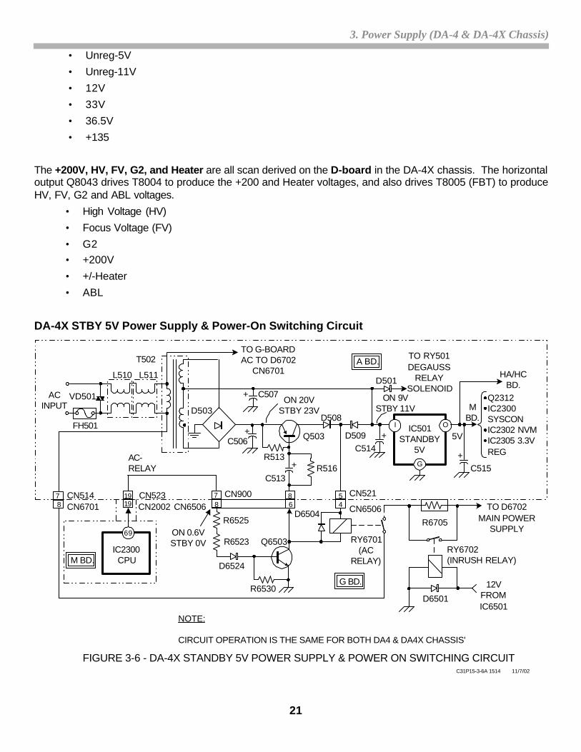
DA-4X STBY 5V Power Supply & Power-On Switching Circuit
22
3. Power Supply (DA-4 & DA-4X Chassis)
Standby 5V Power Supply
Reference Figure 3-6 during the following circuit description:
The Standby Power Supply (located on the A-board) is operational as long as the set is plugged into an AC outlet.AC power is applied to T502 through fuse FH501, and chokes L510 and L511. T502 couples the AC across toD503 rectifier block and filter capacitor C507 (AC is also coupled to Q503 this is part of the power-on switchingcircuit which will be discussed next).
The Standby 5V power supply is a simple conventional full-wave (only two diodes in D503 are used) rectifiercircuit. The resulting DC voltage (13V) is applied to the input pin of IC501 (5V regulator), which then suppliesregulated 5V to the following components:
• IC2300 System Control (M-board)
• IC2302 NVM (M-board)
• IC2305 3.3V Regulator (M-board)
• Q2312 Remote Input Buffer• HA/HC boards (Key Input, LED, and Remote Sensor)
Power-ON Switching Circuit
Reference Figure 3-6 during the following circuit description:
In the Standby mode, System Control (IC2300) is partially powered (using STBY 5V and 3.3V), and waiting for anON command from either the Front Panel Controls (IC2300/pins 93 and 94) or the Remote Control (IC2300/pin7) (circuit not shown).
Once the ON command is received, IC2300/pin 69 (AC_RLY) outputs a high, which is applied to the base ofQ6503, turning Q6503 ON. This completes the ground path for the AC Relay (RY6701) and for the base circuitof Q503.
Q503 turns on and supplies the initial kick voltage and current through D508 to RY6701, closing the relay switchand supplying AC power to the Main Power Supply through Inrush resistor R6705 and D6702. Once C513 in thebase circuit charges completely Q503 turns off; D508 reverse biases and D509 forward biases, supplying a holdvoltage (9V) to keep the relay switch closed in the ON mode.
At this point the Main Power supply is turning ON (operation will be discussed next). The initial AC power to theMain Power Supply is through Inrush resistor R6705, which limits the high surge current that occurs momentarilyat turn ON. Once the secondary voltage UNREG 11V is developed on T6703 in the Main Power Supply, it is fedback to the Inrush Relay (RY6702). RY6702 turns on and bypasses R6705 in the ON mode. R6705 is only inthe circuit during initial power-up of the set.
Troubleshooting Tip:Obviously, if a failure occurs in the 5V Standby Power Supply the unit will not even attempt to turn ON. If thiscondition occurs, check the following components:
1) FH501
2) 13V at IC501 Input Pin (I). If missing, suspect T502, D503, and/or C507
3) 5V at IC501 Output Pin (O). If missing, suspect a defective IC501.4) NOTE: Q503 is used as a current source for the AC relay (RY6701). If the collector/emitter
junction of Q503 becomes an Open circuit, the set will still turn ON (using voltage through D509)and function properly with sufficient AC power input. If the AC power input is weak (Low Voltage~90VAC), the unit will have difficulty turning ON without Q503 functioning properly.
23
3. Power Supply (DA-4 & DA-4X Chassis)
1
14
10
6
18
V-SENSE
VB
VC2
TIMER OCP
IC6701MCZ
3001D
16
15
212
VG(H)
VS
VG(L)
F/B VCI2 8
1
C6711R6728
R6729
9
7
9
4 1
3 2
18
17
16
15
13
124
3 11
10
IC6503DM-58
CONTROL
4 1
5
R6702
D6712
C6726+
C6519+
+ C6723 +
R6732
D6715
R6713
R6731
R6730
R6733
PH6001
+19V
R6518
C6553
D6518
+
T6703
PS6508PS6509
D6511
Q6701
Q6702
G-BOARD
FIGURE 3-7 - DA-4X MAIN POWER SUPPLY CIRCUIT
R6712
D6702 L6701
D6716
C6724+
R6508
+C656036.5V
D6502
UNREG5V
UNREG 7V
R6721
R6714
R6711
R6710
14
R6506
11
A-BOARD
CN514CN6701
IC6501D6514
C6525
PS6507
R6505
D651736V
12V
D6534
D6535
D6515 PS6503
PS6504
PS6505
D6537
D6538
D6503
PS6502
+19V
+15V
-15V
+135V
33V
-19V
UNREG 11V
C6727
11V
0V
18V1.9V
10.6V
146V
2.7V
279V
141V
136V
4.8V
D6519
275Vp-p78kHz
CP31P15-3-7 1513 11/6/02
133V
FROMRY6701&RY6702
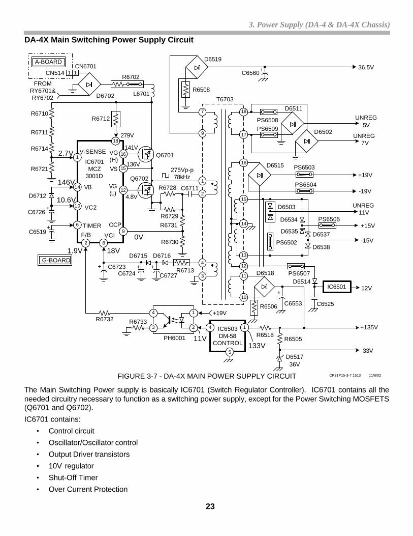
DA-4X Main Switching Power Supply Circuit
The Main Switching Power supply is basically IC6701 (Switch Regulator Controller). IC6701 contains all theneeded circuitry necessary to function as a switching power supply, except for the Power Switching MOSFETS(Q6701 and Q6702).
IC6701 contains:
• Control circuit
• Oscillator/Oscillator control
• Output Driver transistors
• 10V regulator
• Shut-Off Timer
• Over Current Protection
24
3. Power Supply (DA-4 & DA-4X Chassis)
Main Switching Power Supply OperationReference Figure 3-7 for the following circuit description:AC signal is applied to the rectifier block D6702. The AC component is filtered-out by the filter circuit (shown inblock form). A DC voltage of 293V is produced at the output of the filter circuit.
IC6701 Startup Sequence
1) Turn ON voltage: The 279Vdc from the filter circuit is voltage divided by R6710, R6711, R6714 and R6721down to 2.7Vdc. This voltage is applied to IC6701/pin 1 (Vsense) and IC6701 turns ON. IC6701/pin1(Vsense) is also used for OVP protection (IC6701/pin 1 > 8V will trigger OVP).
2) Internal circuit Start Voltage: The 279Vdc also passes through voltage dropping resistors R6702 andR6712, and 291Vdc is applied to IC6701/pin 18. This voltage is used to initially power the internal circuitsand begin oscillations. Note that the 279Vdc from R6702 is connected directly to the Drain of Q6701 andserves as the High-side FET power source.
Internal circuits initially power by IC6501/pin 18
• Internal drive transistors for High-side output FET Q6701
• Oscillator
• Control circuit
• 10V regulator (IC6701/pin 10)Note: The 10V output at IC6701/pin 10 passes through D6712 and supplies power to the internaldriver transistor for the Low-side output FET Q6702
3) Output Oscillations: At this point, initial square-wave oscillations of approximately 125KHz are output atIC6701/ pins 16 and 12. Normal operation frequency is approximately 85KHz.
4) Regulator Feedback: The feedback line is connected to the +135V secondary output. Once IC6701 isturned ON and oscillations begin, the secondary winding at T6703/pin 11 and associated circuitry produces+135. The +135V is applied to IC6503/pin 1 (DM-58 Control).
IC6503 controls the voltage at the PH6001/pin 2, which controls the current output of the optic-couplerPH6001. The amount of current supplied to IC6701/pin 2 depends on how hard PH6001 is turned ON. Innormal operation, a voltage of 1.9Vdc (which is proportional to the amount of current) is present atIC6701/pin 2. The feedback loop is now complete.
5) IC6701 normal operating power supply (VC1): Produced simultaneously with the oscillator feedback isthe operating power source VC1.
IC6701/pin 8 (VC1) is produced using a winding on T6703/pin 4. The AC is rectified, filtered and a DCvoltage of 18V is applied to IC6701/pin 8. Once the 24V is stable, IC6701’s internal control circuitdisconnects (internally) the power source at IC6701/pin 18. All IC6701 internal circuits are now poweredfrom IC6701/pin 8.
Over Current Protection (OCP): ref. Figure 3-7
The current flowing through the switching FETS (Q6701 and Q6702) also passes through T6703/pins 1 and2, C6711 and resistor bank R6728 and R6729. The voltage drop across resistor bank R6728 and R6729 isdirectly proportional to the current through the switching FETS. The voltage drop across R6557 and R6556is further voltage divided by R6731 and R6730 and applied to IC6701/pin 9. The OCP is activated when thevoltage at IC6701/pin 9 exceeds 0.2V. The self-diagnostic indicator will flash four times, pause and thenrepeat.
Over Voltage Protection (OVP) and Under Voltage Protection (UVP): The voltage at IC6701/pin 8 (VC1) ismonitored by circuitry inside IC6701 for Under-voltage and Over-voltage conditions. The two conditions areas follows:
OVP – greater then 33V
25
3. Power Supply (DA-4 & DA-4X Chassis)
UVP – less then 8V
If either of these two conditions occurs at IC6501/pin 8, the unit will go into protection mode. The self-diagnostic indicator will flash four time times, pause and then repeat.
Troubleshooting Tips (ref. Figure 3-3)
NOTE: Follow previously discussed “IC6701 Startup Sequence”. The five steps are in order of occurrence.
NOTE: Use HOT GRND when making measurements on primary side of T6703. This includes allmeasurements on IC6701.
Symptom: Unit goes into protection mode, LED flashes four times.
Check: This indicates either a Vertical deflection or Power Supply problem.
1) Check power supply secondary outputs.
2) If voltages are present and at the proper level, then the problem is in the Vertical deflection drive circuit.
3) If the secondary voltages are low or missing, then the problem is in the power supply.
4) The power supply can be safely tested by unloading the +135v line. Unsolder l6514. This will unload the+135V line of the power supply, but still send necessary feedback to IC6701 for proper power supplyoperation.
5) If the power supply outputs proper secondary voltages after unsoldering l6514, suspect a shorted +135Vline. Check the Horizontal Output transistor (Q505 or 506) for shorted conditions.
6) If the unit still goes into protection mode after unsoldering lC6514, check the following items:
• IC6701/pin 15 (this is midpoint for output MOSFETS Q600 Q6701 and Q6702). A 275Vpp, 78KHzsquare-wave should be present. If the waveform pulses four times and stops, check the nextItem.
• IC6701 Feedback circuit. The amount of current feedback can be determined by monitoring thevoltage drop across R6732. The minimum current feedback is 80uA, which is a minimum voltagedrop of 37.6mV. In normal operation, this voltage drop is approximately 223mV. If the voltagedrop is below 37.6mV, suspect components in the feedback path, e.g. PH602 and IC604. ReferenceFigure 3-7 for proper voltages at these components.
• If no waveform is present when unit is turned ON, then check IC6701/pins 1 and 18 for propervoltages (reference “IC600 Startup Sequence” above).
If these voltages check OK, check IC600/pin 8 for proper voltage of 18V. This is the voltage usedto power IC6701 after initial startup.
If 18V is present at IC6701/pin8, check IC6701/pin 10 for 10.2V. This voltage is developed usingthe 18Vs and a voltage regulator circuit inside IC6701. If 10.2V is missing, suspect a defectiveIC6701. Also check voltage at IC600/pin 14 (Use battery powered DVM for this measurement,and use IC6701/pin 15 (VS) as ground ref.). The voltage at IC6701/pin 14 should be 10V. If thevoltage measured at IC6701/pin 14 is incorrect, check D6712.
• If all the above measurements check OK, suspect a defective IC600.
26
3. Power Supply (DA-4 & DA-4X Chassis)
FIGURE 3-8 - DA-4 & DA-4X REGULATOR INTERCONNECT DIAGRAM10/9/02C31P15-3-8
DA4X ONLY
UNREG 7V+5VIC8010
I
G
O
+15V
*IC8004 (DA4X)
12
11
8
7
4
3
12
11
8
7
4
3
IC650012V REG 12VI
G
O
IC5045V REG 5VI
G
O
IC5023.3V REG 3.3VI
G
O
IC5059V REG 9VI
G
O
UNREG 7V
UNREG 5V
UNREG 11V
D BOARD
A BOARD
DA4 & DA4X
CN524
G-BOARD (DA4X)
D-BOARD (DA4) CN6504
CN6507
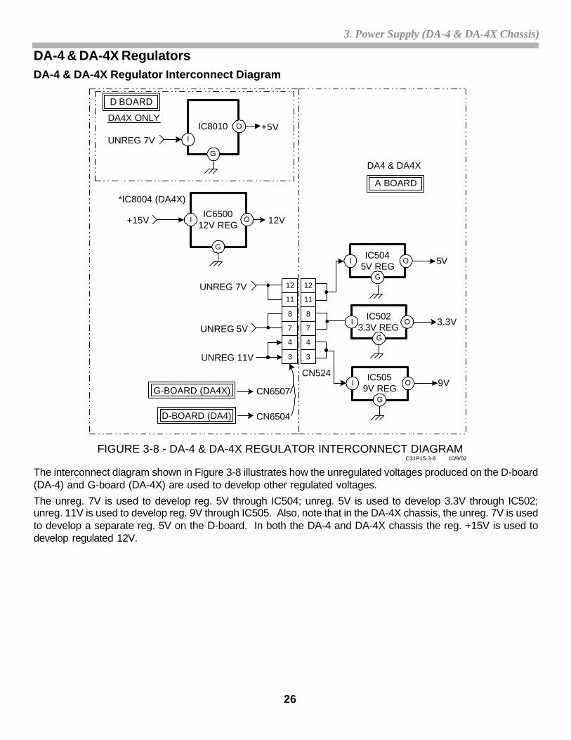
DA-4 & DA-4X RegulatorsDA-4 & DA-4X Regulator Interconnect Diagram
The interconnect diagram shown in Figure 3-8 illustrates how the unregulated voltages produced on the D-board(DA-4) and G-board (DA-4X) are used to develop other regulated voltages.
The unreg. 7V is used to develop reg. 5V through IC504; unreg. 5V is used to develop 3.3V through IC502;unreg. 11V is used to develop reg. 9V through IC505. Also, note that in the DA-4X chassis, the unreg. 7V is usedto develop a separate reg. 5V on the D-board. In both the DA-4 and DA-4X chassis the reg. +15V is used todevelop regulated 12V.
27
4. DA-4 & DA-4X Protection Circuits
Chapter 4 - DA-4 & DA-4X Protection Circuits
FIGURE 4-1 - DA-4 PROTECTION CIRCUITS OVERALL BLOCK 10/30/02C31P15-4-1
CHASSISTEMPERATUREPROTECTION
TH5002
FBTOCP
VIDEO MUTEQ8008
VERTICALDEFLECTIONPROTECTION
IC5004
LOW B+ 5VPROTECTIONIC504, Q527
IK WHITE BAL.PROTECTION
IC9001, IC9002,IC9003
SYSCONIC2300
CRT DRIVEIC2801
(7X)
(2X)B+ OCPQ5004
(7X)
(4X)
(6X)
A BOARD
CH/CX BD.
(5X)
M BOARD
B BOARD
DATAAC RELAY
RY6501
LATCHQ6532Q6530
INRUSHPROTECTION
RELAYRY6502
LOW HVPROTECTION
IC8006
B+ OVPIC6505
FBT OCP(AC SHUT OFF)
Q8007
(7X)(6X) (3X) (7X)
HV POWER SUPPLYIC8002
EXCESSIVE HVPROTECTION
IC8001
HORIZONTALDEFLECTIONPROTECTION
IC8006
HOTGROUNDSECTION
(6X)
(7X)
D BOARD
AC-RELAY
Q6527
V-PROT
IK PROT
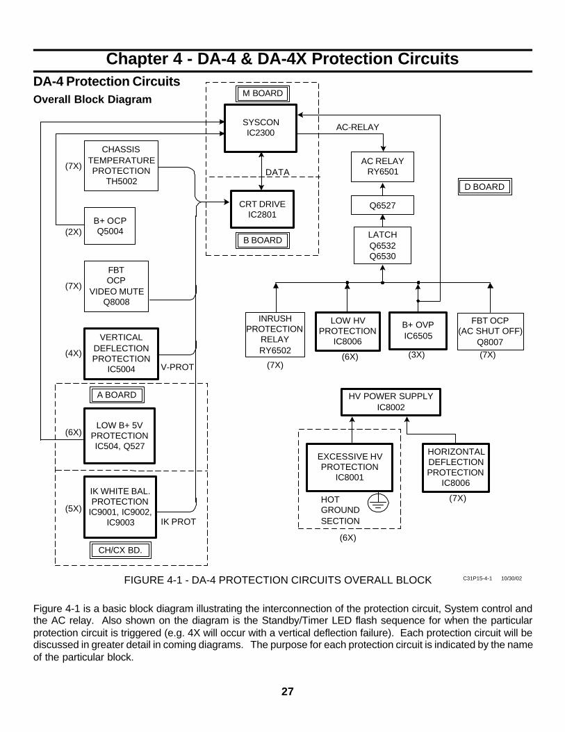
DA-4 Protection CircuitsOverall Block Diagram
Figure 4-1 is a basic block diagram illustrating the interconnection of the protection circuit, System control andthe AC relay. Also shown on the diagram is the Standby/Timer LED flash sequence for when the particularprotection circuit is triggered (e.g. 4X will occur with a vertical deflection failure). Each protection circuit will bediscussed in greater detail in coming diagrams. The purpose for each protection circuit is indicated by the nameof the particular block.
28
4. DA-4 & DA-4X Protection Circuits
The important thing to note on this diagram is the protection circuits that have a direct connection to the CPU andthose that do not. The protection circuits that have a direct connection will produce a more reliable flash sequencee.g. 2X, 3X, 4X, and 6X. The circuits that do not have a direct connection may produce a 7X or 6X flashsequence.
TH5002 is used to monitor the temperature of Q5031 (S-Correction Output). If this transistor should become ashort circuit, the current will increase which causes an increase in temperature. TH5002 detects the rise intemperature, the Video is muted and AC input is disconnected through IC2801 (CRT Drive) and datacommunications with IC2300 (Syscon).
Q5004 monitors the current draw on the +135V line. If the current should increase, video is muted via IC2801and IC2300. Also note that there is a direct connection from the B+ OCP circuit and IC2300 Syscon for quickdisconnection of AC input.
Q8008 monitors the current in the secondary of the FBT using the ABL voltage. If excessive current flows in theFBT, Q8008 is used to mute the video. Q8008 works simultaneously with Q8007, which turns off the AC relay.
IC5004 is the vertical deflection output drive IC. A feedback pulse is produced at IC5004/pin 3. If a verticalfailure occurs, the feedback pulse is not produced and the video is muted (AC input and Audio remain ON).
Q2314 monitors the 5V dc level. If the dc level falls below 4.5V, Q2314 detects this error and the AC input isdisconnected.
IC9001, 9002, and 9003 on the CH/CX board are the cathode drive ICs. Each IC produces a separate IK pulsedirectly proportional to the current in each cathode. The current in each cathode indicates the physical conditionof the cathode. Depending on the cathode condition the set will either increase RGB drive to the cathode or gointo IK Protection mode.
RY6502 is used to bypass the Inrush Current resistor from the AC input circuit after initial set turn-on. If the relayfailures to activate, AC input is disconnected.
IC8006 monitors the HV output. If the HV is low, IC8006 detects this condition and the AC input is disconnected.
IC6505 monitors the +135 voltage level. If the voltage increases, IC6505 will disconnect the AC input.
Q8007 monitors the current in the FBT secondary. If the current increases, Q8007 will disconnect the AC input.Q8007 works simultaneously with Q8008, which mutes the video output.
IC8001 monitors the HV level. NOTE: this circuit is on the HOT (or primary) side of the transformer, so useHOT Ground for measurements. If the HV increases, IC8001 will turn off the HV converter IC8002.
IC8006 monitors the horizontal deflection output drive. If the horizontal deflection stops, IC8006 will turn-off theHV converter IC8002.
29
4. DA-4 & DA-4X Protection Circuits
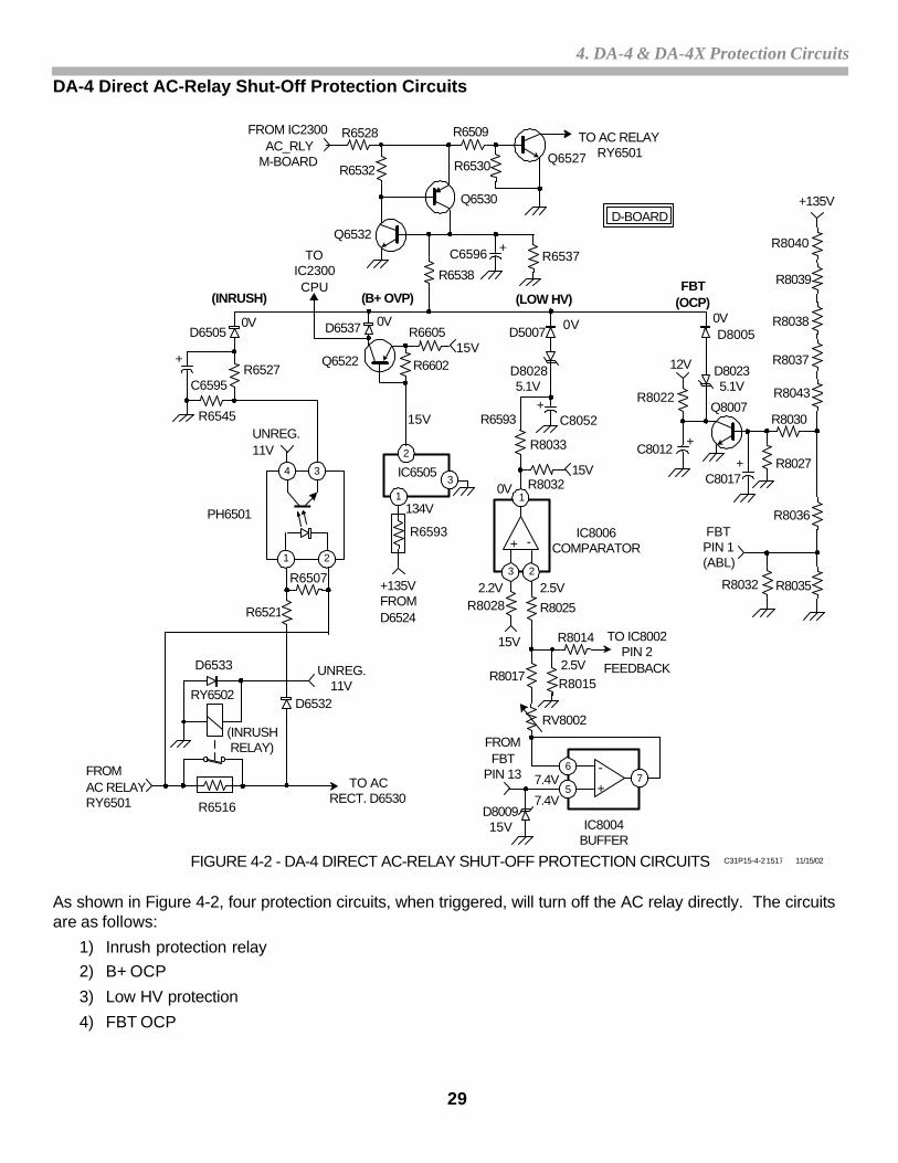
FIGURE 4-2 - DA-4 DIRECT AC-RELAY SHUT-OFF PROTECTION CIRCUITS
+
UNREG.11V
C6595
D6505
TO AC RELAYRY6501
C6596 R6537+
R6538
2
1
IC6505
FROM IC2300 AC_RLYM-BOARD
3
R6593
R8033
1
3 2
IC8006COMPARATOR+ -
R8040
R8039
R8038
R8037
R8043
R8030
R8027C8017
Q8007
R8036
R8035R8032
FBTPIN 1(ABL)
R8022
+135V
D8005
D80235.1V
D80285.1V
R6528
R6532
R6509
Q6527R6530
Q6530
FBT(OCP)(LOW HV)(INRUSH) (B+ OVP)
R6605D6537 D5007
0V15V
R8032
C8052+
+
R8028
R8014
R8017
TO IC8002PIN 2
FEEDBACK
2.2V
2.5V
15V
R6527
FROMFBT
PIN 13
2.5V
C8012 +
134V
+135VFROMD6524
R6602
15V
Q6522
Q6532
15V
C31P15-4-2 1517 11/15/02
76
5
-
+
IC8004BUFFER
RV8002
7.4V
7.4V
D800915V
12V
D-BOARD
TOIC2300CPU
0V0V 0V0V
R6545
R8025
R8015
R6593
FROMAC RELAYRY6501
4
1
3
2
R6507
R6521
D6532RY6502
UNREG.11V
(INRUSHRELAY)
R6516
PH6501
TO ACRECT. D6530
D6533
DA-4 Direct AC-Relay Shut-Off Protection Circuits
As shown in Figure 4-2, four protection circuits, when triggered, will turn off the AC relay directly. The circuitsare as follows:
1) Inrush protection relay2) B+ OCP
3) Low HV protection
4) FBT OCP
30
4. DA-4 & DA-4X Protection Circuits
Inrush Current Relay Protection Circuit
(Reference Figure 4-2)
The current rating of the AC relay (RY65010) is 117mA at 153VAC. To keep the current below 117mA resistorR6515 (Inrush Current Resistor) is in series with the AC input during the initial power-up of the TV. After theinitial power-up current surge, R6516 is bypassed when RY6502 (Inrush Relay) is energized and the switch isclosed.
The operation of RY6502 is monitored using R6516 and PH6501. If RY6502 does not function, a voltage dropwill develop across R6515, which in turn develops a voltage across R6507. The voltage across R6507 turns onthe LED and 11V is output on PH6501/pin 3. D6505 is now forward biased and a High is applied to the base ofQ6532, turning it ON, which then applies a Low to the base Q6530, turning it ON. Q6532 and Q6530 is alatching circuit.
Once the latch is activated, the voltage at the base of Q6527 is reduced and it turns OFF, removing the groundpath for the AC Relay and it turns OFF. The TV shuts down and the Stby/Timer LED flashes a 7X sequence.B+ OVP
(Reference figure 4-2)
The voltage level of the +135V line is monitored using IC6505. If the +135V increases at IC6505/pin 2, thevoltage at IC6505/pin 2 will decrease. Once IC6505/pin 2 decreases by 0.6V, Q6522 will turn ON. D6537 is nowforward biased and a High is applied to the base of Q6532, turning it ON, which then applies a Low to the baseQ6530, turning it ON (activating the latch).
Once the latch is activated, the voltage at the base of Q6527 is reduced and it turns OFF, removing the groundpath for the AC Relay and it turns OFF. The TV shuts down and the Stby/Timer LED flashes a 3X sequence.
Low HV Protection Circuit
(Reference Figure 4-2)The HV level is monitored through the HV Regulator circuit. IC8004 and resistor network RV8002, R8017,R8014 and R8015 are part of the HV regulator circuit. A sample of the HV is output at FBT/pin 13 and is appliedto IC8004/pin 5 (Buffer). Approximately 7.4V is produced at IC8004/pin 7, which is then applied to the resistornetwork. Approximately 2.5V is developed at the junction of R8014, R8015 and R8017.
R8014 is the feedback path for IC8002 (HV Power Supply Converter IC) to keep the HV regulated.
R8025 is the path for the Low HV detection circuit. When the 2.5V at IC8006/pin2 decreases below the referencevoltage 2.2V at IC8006/pin3, a High will be output at IC8006/pin 1 (approximately 14V) through pull-up resistorR8032. Zener diode D8028 (5.1V) will break down. D5007 is now forward biased and a High is applied to thebase of Q6532, turning it ON, which then applies a Low to the base Q6530, turning it ON (activating the latch).
Once the latch is activated, the voltage at the base of Q6527 is reduced and it turns OFF, removing the groundpath for the AC Relay and it turns OFF. The TV shuts down and the Stby/Timer LED flashes a 6X sequence.
FBT Over Current Protection (IK-Prot. 2)
(Reference Figure 4-2)
The secondary current in FBT is monitored by Q8007 at FBT/pin 1 (ABL). The +135V is used as the referencevoltage through the resistor voltage divider consisting of R8040, R8039, R8038, R8037 and R8043. The combinedvoltage drop across R8036 and R8035 is used to turn off Q8007 and trigger the protection circuit. In normaloperation, 0.6V is applied to the base of Q8007, turning it ON and a Low is present at the collector. A High at thecollector is needed to activate the protection mode.
As the current in the FBT secondary increases, the ABL line will increase current through the voltage dividernetwork at the top of R8035 and less current will flow through R8035. The voltage drop across R8035 willdecrease, causing the combined voltage drop across R8036 and R8035 to decrease. At the same time, the 0.6Vat the base of Q8007 is decreasing, which turns OFF Q8007 and a High will be developed at the collectorthrough pull-up resistor R8022. Zener diode D8023 (5.1V) will break down. D8005 is now forward biased and a
31
4. DA-4 & DA-4X Protection Circuits
5
67
2
31
4 1
3 2
FBT
5
C8007
IC8104VREF.
3
2
1
7
6 5
IC8002HV
SWITCHINGCONVERTER
1
16
12
Q8014
R8069
Q8013FBT
T8001
IC8006
IC8001
15V
15VR8072
D8072
C8041
R8078D8001
R8046
R8052
R8016
TOHORIZONTALDEFLECTION
YOKE
15VR8135
R8136 R8137
D81409V
D501815V
-15V
R8011
Q5021BUFFER
Q5025 (BUFFER)
C8021
+
C8006
D80246.2V
Q8004
Q8003
R8001
(HORIZONTALDEFLECTIONPROTECTION)
(EXCESSIVEHV PROTECTION)
19VFROM T6502/PIN 8
V-SENSE
+C8002
4.5V 7.4V
2.2V
2.5V
2.2V
2.5V
2.4V
FIGURE 4-3 - DA-4 EXCESSIVE HV AND HORIZONTALDEFLECTION PROTECTION CIRCUITS
+
+
+-
-
-
D-BOARD
C31P15-4-3 1518 11/12/02
A
B
0V
0V
NOTE:HOT GROUNDSECTION
HDRIVE
Q5030H-OUT
C5058
C5059
C5060
13TO LOW HV PROTREF. FIGURE 4-2
FOR DETAIL
PH8001
R5118
High is applied to the base of Q6532, turning it ON, which then applies a Low to the base Q6530, turning it ON(activating the latch).
Once the latch is activated, the voltage at the base of Q6527 is reduced and it turns OFF, removing the groundpath for the AC Relay and it turns OFF. The TV shuts down and the Stby/Timer LED flashes a 7X sequence.
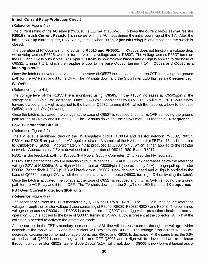
DA-4 Excessive HV and horizontal Deflection Protection Circuits
Excessive HV Circuit(Reference Figure 4-3)
The HV is monitored at FBT/pin 5 using two comparator circuits (A & B) located in IC8001. Comparator A will betriggered when there is a sustained excessive HV (or gradual HV increase), and comparator B will trigger on amomentary (or fast increase) HV surge. Another way to look at these comparators circuits is that they arebackup circuits for each other (redundant circuits) to ensure shutdown under any excessive HV condition.
32
4. DA-4 & DA-4X Protection Circuits
Both comparators receive a sample of the HV from FBT/pin 5, which is input to IC8001/pin 5 and IC8001/pin3. Areference voltage (Vref) of 2.2V is developed at IC8014/pin 3 and applied to IC8001/pins 2 and 6. Once thevoltage at either IC8001/pin 5 or 3 increases above the reference voltage due to an excessive HV conditions, aHigh will be output at either IC8001/pin 7 or 1. The High output will turn ON either Q8004 or Q8003, which willthen apply a Low to IC8002/pin 1 (V-sense) turning the HV power supply converter IC OFF. Drive to the FBT willstop and HV will not be developed.
The TV shuts down and the Stby/Timer LED flashes a 6X sequence.
Horizontal Deflection Protection
(Reference Figure 4-3)
A sample of the Horizontal drive pulse is taken off the top of C5060. The pulse at this point is amplitude limitedusing D5018 to 15V. The sample pulse is first buffer by Q5021 and then applied to comparator IC8006/pin 5through D8140. Approximately 7.4V is developed at IC8006/pin 5, making it more positive then the referencevoltage on IC8006/pin 6 (4.5V). This condition causes a High (15V) to be produced at the output of the comparatorIC8006/pin7. The 15V from IC8006/pin 7 is applied to the cathode side of the LED PH8001/pin 2, and 15V is alsoapplied to the anode side of the LED PH8001/pin 1. So, the LED is OFF and the collector/emitter junction atPH8001/pins 4 and 3 is open. 2.4V is present at PH8001/pin 4.
If the horizontal drive to the deflection yoke (possible defective Q5030) were to cease, there would be no samplepulse applied to IC8006/pin 5, and IC8006/pin 5 will go to 0V. This condition will cause IC8006/pin 7 to go Low.This Low is applied to the cathode of the LED PH8001/pin 2, the LED turns ON and the collector/emitter junctionPH8001/pins 3 and 4 conduct applying ground to IC8002/pin 1 (V-Sense). This turns the HV power supplyconverter IC8002 OFF and no drive to the FBT (HV output stops). With no drive to T8001, there will be no outputon T8001/pin 13. T8001/pin 13 is connected to IC8004/pin 7 and outputs a low to IC8006/pin 2. This will causea high to be output at IC8006/pin 1. This high will cause D8028 to break-over and a high will be applied to thelatch circuit of Q6532 & Q6530, and the AC relay will be shut-off.
The TV shuts down and the Stby/Timer LED flashes a 7X sequence.
33
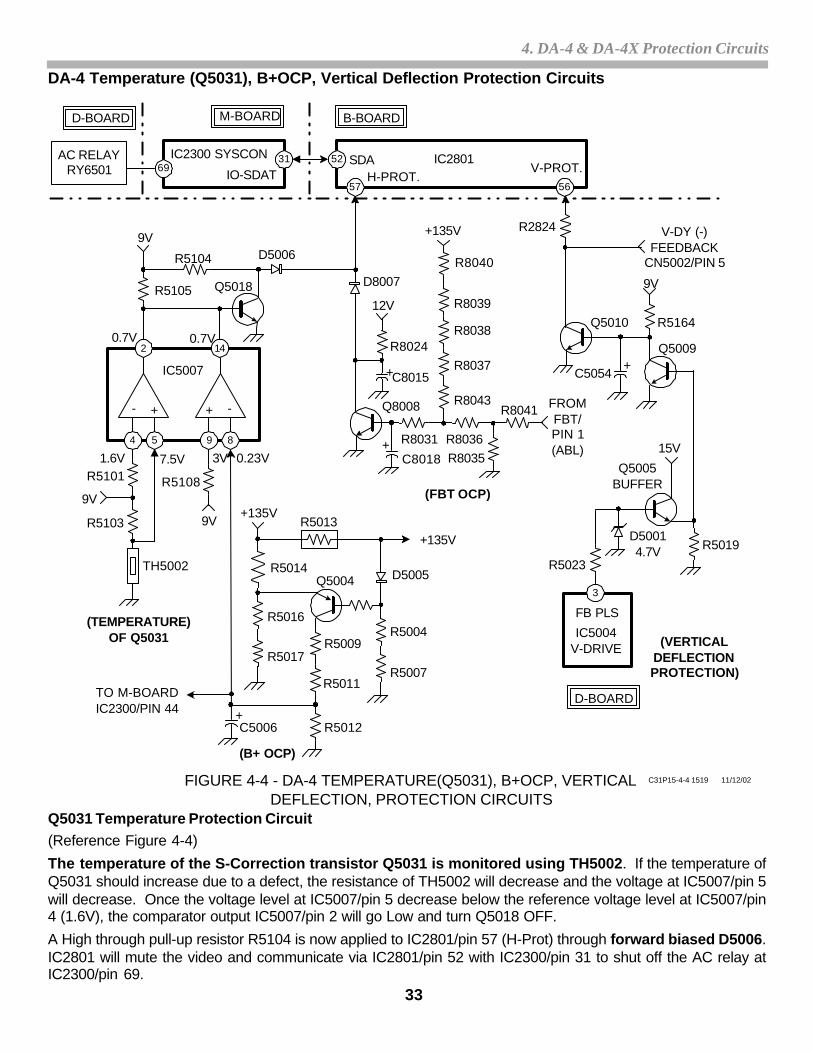
4. DA-4 & DA-4X Protection Circuits
FIGURE 4-4 - DA-4 TEMPERATURE(Q5031), B+OCP, VERTICALDEFLECTION, PROTECTION CIRCUITS
IC5007
+
89
14
54
2
++ --
+
57 56
3
IC5004V-DRIVE
FB PLS
+135V
+135V
H-PROT.IC2801
IO-SDAT
IC2300 SYSCON SDA5231
R5108
R5104
R5105 Q5018
D5006
D8007
9V
0.7V
R5023
D50014.7V
15V
TH5002
R5103
9V
R5101
9V
FROMFBT/PIN 1(ABL)
R5013
Q8008
C8018
R8031 R8036R8035
+135V
D5005
R5004
R5007
C5006
R5014
R5016
R5017R5009
R5011
R5012
Q5004
TO M-BOARDIC2300/PIN 44
R8040
R8039
R8038
R8037
R8043
R2824
Q5010 R5164
9V
Q5009+
C5054
Q5005BUFFER
M-BOARD B-BOARD
V-PROT.
(FBT OCP)
D-BOARD
R5019
1.6V 7.5V 3V 0.23V
(VERTICALDEFLECTIONPROTECTION)
(B+ OCP)
(TEMPERATURE)OF Q5031
C31P15-4-4 1519 11/12/02
0.7V
D-BOARD
69AC RELAY
RY6501
V-DY (-)FEEDBACK
CN5002/PIN 5
R8024
+
12V
C8015
R8041
DA-4 Temperature (Q5031), B+OCP, Vertical Deflection Protection Circuits
Q5031 Temperature Protection Circuit(Reference Figure 4-4)
The temperature of the S-Correction transistor Q5031 is monitored using TH5002. If the temperature ofQ5031 should increase due to a defect, the resistance of TH5002 will decrease and the voltage at IC5007/pin 5will decrease. Once the voltage level at IC5007/pin 5 decrease below the reference voltage level at IC5007/pin4 (1.6V), the comparator output IC5007/pin 2 will go Low and turn Q5018 OFF.
A High through pull-up resistor R5104 is now applied to IC2801/pin 57 (H-Prot) through forward biased D5006.IC2801 will mute the video and communicate via IC2801/pin 52 with IC2300/pin 31 to shut off the AC relay atIC2300/pin 69.
34
4. DA-4 & DA-4X Protection Circuits
The TV video is muted, the AC relay shuts down and the Stby/Timer LED flashes a 7X sequence.
B+OCP Protection Circuit
(Reference figure 4-4)
The current in the +135V line is monitored using R5013 and Q5004. R5013 is the current sensing resistor. Thecurrent in the +135V line flows directly through R5013. The voltage drop across R5013 in normal operation isvery low, approximately 0.2V. So, the +135V is passed with very little loss in normal operation. The voltage onthe left side is basically equal to the voltage on the right side of R5013, and because R5013 is connected acrossthe base/emitter junction of Q5004, there is no 0.6V difference across the junction and Q5004 is OFF.
When the current in the +135V line begins to increase due to a defect, the voltage drop across R5013 will alsoincrease. Because of the increased voltage drop across R5013, the voltage on the left side of R5013 will remainconstant but the voltage on the right side of R5013 will decrease. The decreased voltage on the right side isapplied to the base of Q5004 through D5005. Once the voltage drop across R5013 is large enough to cause a0.6V difference across Q5004 base/emitter junction, Q5004 turns ON.Current now flows through the voltage divider consisting of R5009, R5011 and R5012. The voltage drop acrossR5012 is applied to IC5007/pin 8, causing IC5007/pin 8 to become more positive then the reference voltage atIC5007/pin 9 (3V). The output IC5007/pin 14 will go Low and turn Q5018 OFF.
A High through pull-up resistor R5104 is now applied to IC2801/pin 57 (H-Prot) through forward biased D5006.IC2801 will mute the video and communicate via IC2801/pin 52 with IC2300/pin 31 to shut off the AC relay atIC2300/pin 69.
The TV video is muted, the AC relay shuts down and the Stby/Timer LED flashes a 2X sequence.
FBT Over Current Protection Circuit (IK Prot. 1)
(Reference Figure 4-4)
The secondary current in FBT is monitored by Q8008 at FBT/pin 1 (ABL). The +135V is used as the referencevoltage through the resistor voltage divider consisting of R8040, R8039, R8038, R8037 and R8043. The combinedvoltage drop across R8036 and R8035 is used to turn off Q8008 and trigger the protection circuit. In normaloperation, 0.6V is applied to the base of Q8008, turning it ON and a Low is present at the collector. A High at thecollector is needed to activate the protection mode.
As the current in the FBT secondary increases, the ABL line will increase current through the voltage dividernetwork at the top of R8035 and less current will flow through R8035. The voltage drop across R8035 willdecrease, causing the combined voltage drop across R8036 and R8035 to decrease. At the same time, the 0.6Vat the base of Q8007 is decreasing, which turns OFF Q8007 and a High will be developed at the collectorthrough pull-up resistor R8022. D8007 is now forward biased through pull-up resistor R8024 and a High isapplied to IC2801/pin 57. IC2801 will mute the video and communicate via IC2801/pin 52 with IC2300/pin 31 toshut off the AC relay at IC2300/pin 69.
The TV video is muted, the AC relay shuts down and the Stby/Timer LED flashes a 7X sequence.
Vertical Deflection Protection Circuit
(Reference Figure 4-4)
The operation of the vertical deflection circuit is monitored using the feedback pulse developed at IC5004/pin 3(vertical drive IC). The pulse is amplitude limited using D5001 (4.7V Zener diode). The pulse passes throughbuffer Q5005 and is applied to the base of Q5009, turning it ON, while applying a Low to the base of Q5010,turning it OFF. With Q5010 OFF, the V-DY feedback will be applied to IC2801/pin 56 indicating proper verticaldeflection operation.
If the Vertical deflection should cease due to a defect, the feedback pulse at IC5004/pin 3 will not be developed(no pulse through Q5005 buffer), Q5009 will turn OFF and Q5010 will turn ON. The V-DY will go to groundIC2801/pin 56 detects the missing V-DY and places the TV in vertical shut down.
35
4. DA-4 & DA-4X Protection Circuits
C31P15-4-5 10/28/02FIGURE 4-5 - DA-4 REG. 5V AND WHITE BALANCE PROTECTION CIRCUITS
IC2300 SYSCON
43 81
R2375
R2399
R2300
D23103.6V
C2361
2.8V
I-LB-ERR IO-SDAT
IC5045V REG.
O
R2298
I
G
UNREG 7V
A BOARD
52
B BOARD
24
R900612VR9013
C9017
R9068
R9012
Q9007
R9039
11V12V
10.6V
Q9015
R902011V12V
Q9013
R902511V12V
(WHITE BALANCE PROTECTION)
IC9001RED
7
IK
IC9002GREEN
7
IK
IC9003BLUE
7
IK
NOTE: IK_OUT ON HS MODELSIS IC9001, 9002, 9003/PIN 5
NOTE: 11VWITHWHITERASTER
CH/CX BOARD
M BOARD
(REG. 5VPROTECTION)
+Q9001
12V
IC2801CRT DRIVE
IK_IN
69 AC RELAYRY6501
D BOARD
R9012
Q2314
In vertical shut down mode, only the video is muted, the AC power and Audio remain ON and the Stby/Timer LED flashes a 4X sequence.
DA-4 Regulated 5V and White Balance Protection Circuit
Regulated 5V Protection Circuit(Reference Figure 4-5)
The regulated 5V line is monitored using Q2314 and Zener diode D2310 (3.6V) on the M-board. The output ofthe 5V regulator IC504 is applied to the emitter of Q2314. In normal operation Q2314 is turned ON and D2310is conducting, holding the base at 3.6V. Approximately 2.8V is applied to System Control IC2300/pin 43, indicatingproper level of the regulated 5V line.
If the 5V line falls below approximately 4.5V at the emitter of Q2314, D2310 will stop conducting, Q2314 will turnOFF and a Low will be applied to IC2300/pin 43. IC2300/pin 69 will then turn OFF the AC relay.
The AC relay shuts down and the Stby/Timer LED flashes a 6X sequence.
36
4. DA-4 & DA-4X Protection Circuits
White Balance Protection Circuit (IK Protection)
(Reference Figure 4-5)
The condition of each CRT cathode (RGB) must be monitored in order to maintain optimal white balance. Eachcathode is monitored by the individual driver IC9001, 9002 and 9003 on the CH/CX board. Each driver IC9001/pin 7, IC9002/pin 7 and IC9003/pin 7 develops an IK feedback pulse, which is directly proportional to the currentdrawn by each cathode in the CRT. The IK feedback pulse passes through buffer transistors Q9007, Q9015 andQ9013, and then the sequence of the three IK feedback pulses is applied to the base of buffer Q9001.
The three IK feedback pulses are sequentially fed into IC2801/pin 24 and monitored for amplitude variations. Ifthe IK feedback pulse is Low in amplitude or is missing, this indicates a weak or defective cathode. IC2801/pin24 will detect this condition and the unit will go into IK protection mode.
The TV video is muted, the AC relay will remain ON and the Stby/Timer LED flashes a 5X sequence.
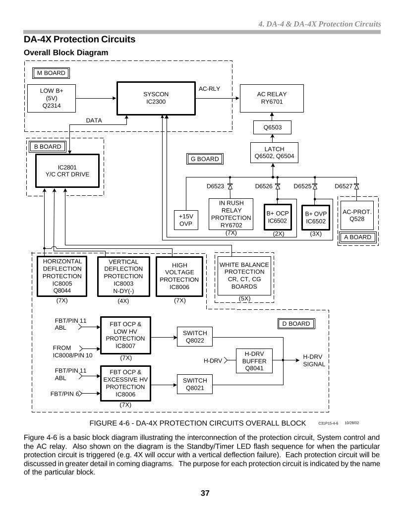
37
4. DA-4 & DA-4X Protection Circuits
LOW B+(5V)
Q2314
M BOARD
AC RELAYRY6701
LATCHQ6502, Q6504
+15VOVP
IN RUSHRELAY
PROTECTIONRY6702
B+ OCPIC6502
B+ OVPIC6502
AC-PROT.Q528
Q6503
A BOARD
IC2801Y/C CRT DRIVE
HORIZONTALDEFLECTIONPROTECTION
IC8005Q8044
VERTICALDEFLECTIONPROTECTION
IC8003N-DY(-)
HIGHVOLTAGE
PROTECTIONIC8006
WHITE BALANCEPROTECTION
CR, CT, CGBOARDS
B BOARD
G BOARD
H-DRVSIGNAL
FBT OCP &LOW HV
PROTECTIONIC8007
FBT OCP &EXCESSIVE HVPROTECTION
IC8006
SWITCHQ8022
SWITCHQ8021
H-DRVBUFFERQ8041
D BOARDFBT/PIN 11ABL
FROMIC8008/PIN 10
FBT/PIN 11ABL
FBT/PIN 6
FIGURE 4-6 - DA-4X PROTECTION CIRCUITS OVERALL BLOCK C31P15-4-6 10/28/02
AC-RLYSYSCONIC2300
D6523 D6526 D6525 D6527
H-DRV
(7X) (2X) (3X)
(7X) (4X) (7X) (5X)
(7X)
(7X)
DATA
DA-4X Protection CircuitsOverall Block Diagram
Figure 4-6 is a basic block diagram illustrating the interconnection of the protection circuit, System control andthe AC relay. Also shown on the diagram is the Standby/Timer LED flash sequence for when the particularprotection circuit is triggered (e.g. 4X will occur with a vertical deflection failure). Each protection circuit will bediscussed in greater detail in coming diagrams. The purpose for each protection circuit is indicated by the nameof the particular block.
38
4. DA-4 & DA-4X Protection Circuits
(Reference Figure 4-6)
Q2314 monitors the 5V dc level. If the dc level falls below 4.5V, Q2314 detects this error and the AC input isdisconnected.RY6702 is used to remove the Inrush Current resistor from the AC input circuit after initial set turn-on. If the relayfailures to activate, AC input is disconnected.
IC9101, 9201 and 9301 on the CR/CB/CG boards are the cathode drive ICs. Each IC produces a separate IKpulse directly proportional to the current in each cathode. The current in each cathode indicates the physicalcondition of the cathode. Depending on the cathode condition, the set will either increase RGB drive to thecathode or go into IK Protection mode.
+15V OVP monitors the 15V line for excessive voltage condition.
IC6502 is used to monitor both +135V OVP and OCP conditions.
Q528 on the A-board. If AC is not present at the input to the Standby 5V circuit, Q528 will activate the Latch andshut down the TV.
IC8005 and Q8044 monitor the horizontal deflection operation.
IC8003 and V-DY(-) IC8003 is the vertical drive IC that drives the deflection yoke (DY). The low side of thedeflection yoke is monitored for proper vertical operation.
IC8006 and IC8007 monitor three separate circuits: Low HV, Excessive HV and FBT OCP.
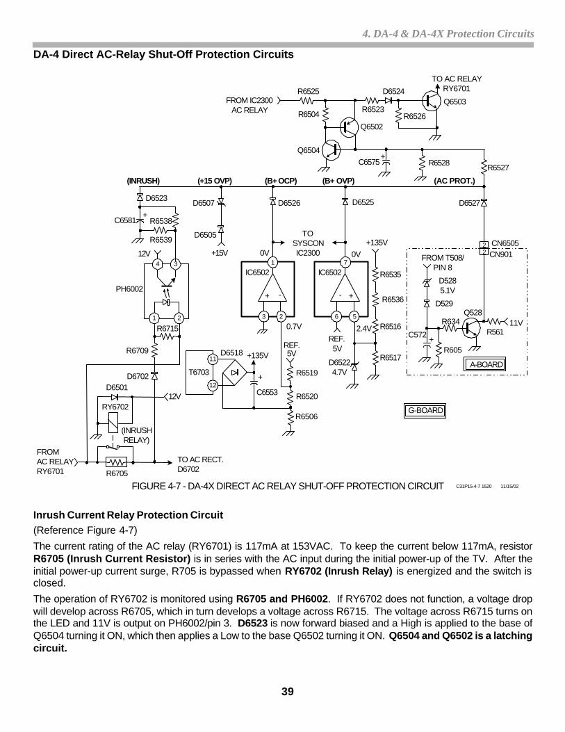
39
4. DA-4 & DA-4X Protection Circuits
FROMAC RELAYRY6701
7
6 5
IC6502
+-
1
3 2
IC6502
+ -
T6703
+135V
REF.5V
4
1
3
2
TOSYSCONIC2300
D6523
12V
+C6581
R6539
R6538
D6507
D6505
+15V
D6526 D6527
R6715
R6709
D6702
D6518
C6553
+
PH6002
2.4V
D65224.7V
R6517
R6516
R6536
R6535
+135V
0.7V
0V0V22
FROM T508/PIN 8
D529
D5285.1V
R634
R605
C572 +
CN6505CN901
Q528
A-BOARD
G-BOARD
R6528+
C6575
R6525
R6523
D6524Q6503
R6504
Q6502
Q6504
R6526
R6527
FROM IC2300AC RELAY
TO AC RELAYRY6701
(INRUSH) (+15 OVP)
D6525
(B+ OCP) (B+ OVP) (AC PROT.)
TO AC RECT.D6702
FIGURE 4-7 - DA-4X DIRECT AC RELAY SHUT-OFF PROTECTION CIRCUIT C31P15-4-7 1520 11/15/02
11
12
R56111V
R6506
R6520
R6519
REF.5V
R6705
RY670212V
D6501
(INRUSHRELAY)
DA-4 Direct AC-Relay Shut-Off Protection Circuits
Inrush Current Relay Protection Circuit(Reference Figure 4-7)
The current rating of the AC relay (RY6701) is 117mA at 153VAC. To keep the current below 117mA, resistorR6705 (Inrush Current Resistor) is in series with the AC input during the initial power-up of the TV. After theinitial power-up current surge, R705 is bypassed when RY6702 (Inrush Relay) is energized and the switch isclosed.
The operation of RY6702 is monitored using R6705 and PH6002. If RY6702 does not function, a voltage dropwill develop across R6705, which in turn develops a voltage across R6715. The voltage across R6715 turns onthe LED and 11V is output on PH6002/pin 3. D6523 is now forward biased and a High is applied to the base ofQ6504 turning it ON, which then applies a Low to the base Q6502 turning it ON. Q6504 and Q6502 is a latchingcircuit.
40
4. DA-4 & DA-4X Protection Circuits
Once the latch is activated, the voltage at the base of Q6503 is reduced and it turns OFF, removing the groundpath for the AC Relay and it turns OFF. The TV shuts down and the Stby/Timer LED flashes a 7X sequence
+15 OVP(Reference Figure 4-7)
The circuit monitoring the condition of the +15V line is a simple 20V zener diode. If the +15V line increasesabove 20.6V, the Latch will be activated and the AC relay will be shut OFF.
B+OCP
(Reference Figure 4-7)
The current is monitored in the +135V line using resistor R6506 located in the ground-side of the +135V circuit.If the current increases in the +135V line, the current through R6506 will also increase, but because of thedirection of the current through R6506, a negative voltage is developed an IC6502/pin 2. IC6502/pin 3 (Grnd)will be now more positive then the negative IC6502/pin 2. a High is produced at IC6502/pin 1 and D6526 isforward biased. The latch is activated and the AC relay is turned OFF. Note that the High from IC6502/pin1 isalso sent to System Control IC2300 to activate self-diagnostics.
B+OVP
(Reference Figure 4-7)
The B+ OVP circuit monitors the voltage level of the +135V through the voltage divider network consisting ofR6535, R6536, R6516 and R6517. If the +135V should rise, so will the voltage drop across R6517and thevoltage at IC6502/pin 5. Once the voltage at IC6502/pin 5 goes more positive then IC6502/pin 6, a High will beproduced at IC6502/pin 7 and D6525 will be forward biased. The Latch will activate and the AC relay will be shutOFF. Note that the High from IC6502/pin7 is also sent to System Control IC2300 to activate self-diagnostics.
AC PROT
(Reference Figure 4-7)
The AC input to the Standby 5V circuit is monitored through D528, D529 and Q528. In normal operation D528 isin break-over mode and Q528 in turned ON. If the AC input is missing, Q528 will turn OFF and a High willforward bias D6527. the Latch will be activated and the AC relay will be shut OFF.
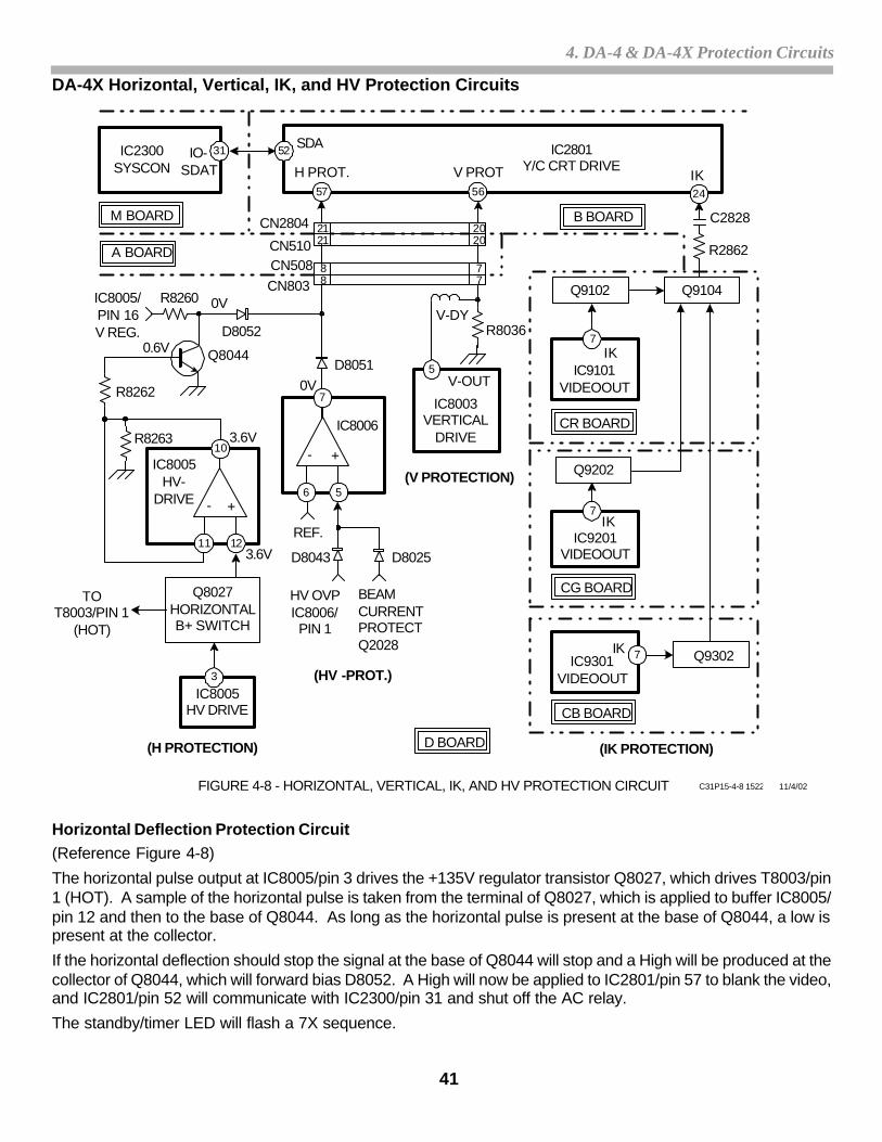
41
4. DA-4 & DA-4X Protection Circuits
Q9202
TOT8003/PIN 1
(HOT)
10
11 12
IC8005HV-
DRIVE +-
0V
Q8027HORIZONTALB+ SWITCH
7
6 5
IC8006
+-
88
2121
77
2020
5
IC8003VERTICAL
DRIVE
V-OUT
IC8005HV DRIVE
3
IC2801Y/C CRT DRIVE
SDA
H PROT. V PROT IK57 56
5231IC2300SYSCON
IO-SDAT
Q9102
7
IC9101VIDEOOUT
IK
B BOARDM BOARD
CR BOARD
CG BOARD
CB BOARD
Q9104
24
IC9201VIDEOOUT
IK
Q9302IC9301VIDEOOUT
IK 7
7
A BOARD
D BOARD
D8051
D8052
R8263
R8262
Q8044
R8260
R8036V-DY
D8025D8043
REF.
R2862
C2828CN2804
CN508CN803
CN510
IC8005/PIN 16V REG.
(IK PROTECTION)
(HV -PROT.)
(V PROTECTION)
(H PROTECTION)
BEAMCURRENTPROTECTQ2028
HV OVPIC8006/PIN 1
FIGURE 4-8 - HORIZONTAL, VERTICAL, IK, AND HV PROTECTION CIRCUIT C31P15-4-8 1522 11/4/02
3.6V
3.6V
0.6V
0V
DA-4X Horizontal, Vertical, IK, and HV Protection Circuits
Horizontal Deflection Protection Circuit(Reference Figure 4-8)
The horizontal pulse output at IC8005/pin 3 drives the +135V regulator transistor Q8027, which drives T8003/pin1 (HOT). A sample of the horizontal pulse is taken from the terminal of Q8027, which is applied to buffer IC8005/pin 12 and then to the base of Q8044. As long as the horizontal pulse is present at the base of Q8044, a low ispresent at the collector.
If the horizontal deflection should stop the signal at the base of Q8044 will stop and a High will be produced at thecollector of Q8044, which will forward bias D8052. A High will now be applied to IC2801/pin 57 to blank the video,and IC2801/pin 52 will communicate with IC2300/pin 31 and shut off the AC relay.
The standby/timer LED will flash a 7X sequence.
42
4. DA-4 & DA-4X Protection Circuits
HV Protection
(Reference Figure 4-8)
Also attached to the H-Prot. input IC2801/pin 57 is the HV-PROT. This circuit is actually monitoring two functions:HV OVP and Beam Current through D8043 and D8025 respectively. If an excessive HV or Beam current conditionshould occur, IC8006/pin 5 will go High, which will cause IC8006/pin 7 to output a High. The High will forwardbias D8051 and a High will now be applied to IC2801/pin 57 to blank the video. IC2801/pin 52 will then communicatewith IC2300/pin 31 and shut off the AC relay. The standby/timer LED will flash a 7X sequence.
Vertical Deflection Protection Circuit
(Reference Figure 4-8)
IC2801/pin 56 monitors the low side of the vertical deflection coil [V-DY (-)]. IC8003/pin 5 drives the high side ofthe V-DY, while the other side goes to ground through R8036. A small vertical feedback signal is developedacross R8036, which is applied to IC2801/pin 56.
If the vertical deflection circuit should fail (no drive to V-DY), IC2801/pin 56 will detect the missing verticalfeedback signal and blank the video output to the CRT. The TV will be placed in Vertical shutdown and thestandby/timer LED will flash a 4X sequence. The AC Power and Audio will remain ON.
IK (White Balance) Protection Circuit
(Reference Figure 4-8)
Each CRT driver IC9101, 9201 and 9301/pin 7 (located on the CR, CG, and CB boards) produces an IK feedbackpulse directly proportional to the current in each cathode (which indicates the condition of the cathode). All threeIK feedback pulses are combined at Q9104 on the CR board and sent back sequentially to IC2801/pin 24.
Each pulse is monitored for level by IC2801/pin 24. If a pulse is low, IC2801/pin 52 will detect a weakenedcathode and IC2801 will increase the drive signal to that weakened cathode until optimal white balance is achieved.If white balance cannot be achieve within two seconds then IC2801/pin 52 will communicate with IC2300/pin 31and the TV will go into IK protection mode. The video to the CRT will be blanked and the standby/timer LEDwill flash a 5X sequence. The AC power and Audio will remain ON.
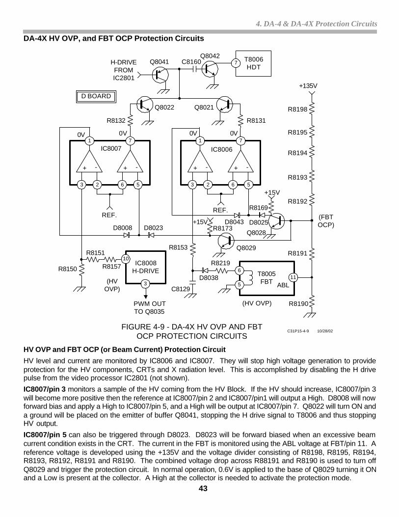
43
4. DA-4 & DA-4X Protection Circuits
T8006HDT
7
6 5
IC8007
+ -
0V1
3 2
+ -
0V7
6 5
IC8006
+ -
0V1
3 2
+ -
0V
IC8008H-DRIVE
10
3
6
5
T8005FBT ABL
11
7
REF.REF.
R8198
R8195
R8194
R8193
R8192
R8191
R8190
Q8029
D8025D8043
R8153
C8129
D8038
R8219
D8008 D8023
Q8022 Q8021
Q8042C8160Q8041
R8151
R8157R8150
PWM OUTTO Q8035
(FBTOCP)
(HV OVP)
H-DRIVEFROMIC2801
+135V
FIGURE 4-9 - DA-4X HV OVP AND FBTOCP PROTECTION CIRCUITS
D BOARD
C31P15-4-9 10/28/02
R8131R8132
Q8028
(HVOVP)
R8169
+15V
+15VR8173
DA-4X HV OVP, and FBT OCP Protection Circuits
HV OVP and FBT OCP (or Beam Current) Protection Circuit
HV level and current are monitored by IC8006 and IC8007. They will stop high voltage generation to provideprotection for the HV components, CRTs and X radiation level. This is accomplished by disabling the H drivepulse from the video processor IC2801 (not shown).
IC8007/pin 3 monitors a sample of the HV coming from the HV Block. If the HV should increase, IC8007/pin 3will become more positive then the reference at IC8007/pin 2 and IC8007/pin1 will output a High. D8008 will nowforward bias and apply a High to IC8007/pin 5, and a High will be output at IC8007/pin 7. Q8022 will turn ON anda ground will be placed on the emitter of buffer Q8041, stopping the H drive signal to T8006 and thus stoppingHV output.
IC8007/pin 5 can also be triggered through D8023. D8023 will be forward biased when an excessive beamcurrent condition exists in the CRT. The current in the FBT is monitored using the ABL voltage at FBT/pin 11. Areference voltage is developed using the +135V and the voltage divider consisting of R8198, R8195, R8194,R8193, R8192, R8191 and R8190. The combined voltage drop across R88191 and R8190 is used to turn offQ8029 and trigger the protection circuit. In normal operation, 0.6V is applied to the base of Q8029 turning it ONand a Low is present at the collector. A High at the collector is needed to activate the protection mode.
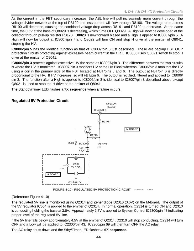
44
4. DA-4 & DA-4X Protection Circuits
FIGURE 4-10 - REGULATED 5V PROTECTION CIRCUIT C31P15-4-10 11/12/02
SYSCONIC2300
43
IC5045V REG.
O
G
IA BOARD
M BOARD
(I-LB-ERR)
R2375
R2299
C2361
Q2314
R2298 R2300
D23103.6V
UNREG. 7V
As the current in the FBT secondary increases, the ABL line will pull increasingly more current through thevoltage divider network at the top of R8190 and less current will flow through R8190. The voltage drop acrossR8190 will decrease, causing the combined voltage drop across R8191 and R8190 to decrease. At the sametime, the 0.6V at the base of Q8029 is decreasing, which turns OFF Q8029. A High will now be developed at thecollector through pull-up resistor R8173. D8023 is now forward biased and a High is applied to IC8007/pin 5. AHigh will now be output at IC8007/pin 7 and Q8022 will turn ON and stop H drive at the emitter of Q8041,stopping the HV.
IC8006/pin 5 has the identical function as that of IC8007/pin 5 just described. These are backup FBT OCPprotection circuits protecting against excessive beam current in the CRT. IC8006 uses Q8021 switch to stop Hdrive at the emitter of Q8041.
IC8006/pin 3 protects against excessive HV the same as IC8007/pin 3. The difference between the two circuitsis where the HV is monitored. IC8007/pin 3 monitors HV at the HV Block whereas IC8006/pin 3 monitors the HVusing a coil in the primary side of the FBT located at FBT/pins 5 and 6. The output at FBT/pin 6 is directlyproportional to the HV. If HV increases, so will FBT/pin 6. The output is rectified, filtered and applied to IC8006/pin 3. The function after a High is applied to IC8006/pin 3 is identical to IC8007/pin 3 described above exceptQ8021 is used to stop the H drive at the emitter of Q8041.
The Standby/Timer LED flashes a 7X sequence when a failure occurs.
Regulated 5V Protection Circuit
(Reference Figure 4-10)
The regulated 5V line is monitored using Q2314 and Zener diode D2310 (3.6V) on the M-board. The output ofthe 5V regulator IC504 is applied to the emitter of Q2314. In normal operation, Q2314 is turned ON and D2310is conducting holding the base at 3.6V. Approximately 2.8V is applied to System Control IC2300/pin 43 indicatingproper level of the regulated 5V line.
If the 5V line falls below approximately 4.5V at the emitter of Q2314, D2310 will stop conducting, Q2314 will turnOFF and a Low will be applied to IC2300/pin 43. IC2300/pin 69 will then turn OFF the AC relay.
The AC relay shuts down and the Stby/Timer LED flashes a 6X sequence.
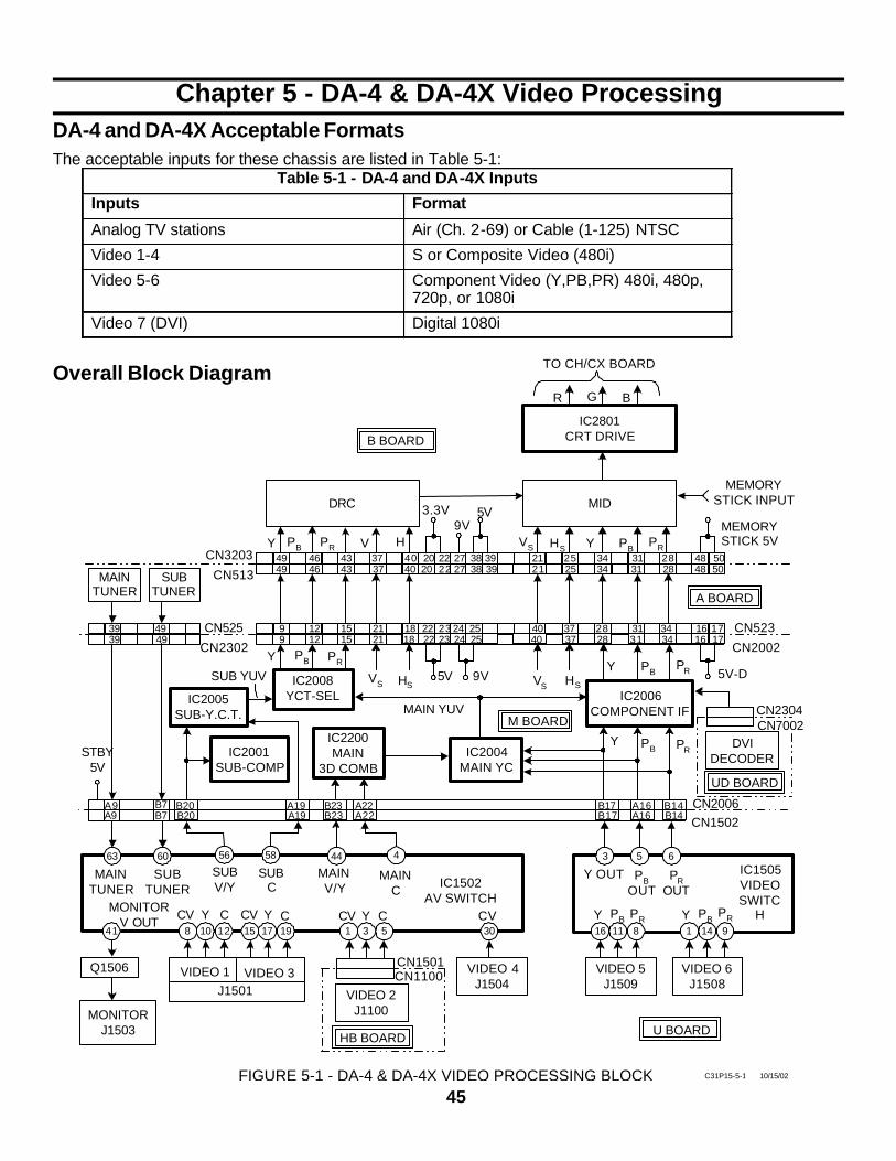
45
5. DA-4 & DA-4X Video Processing
Chapter 5 - DA-4 & DA-4X Video Processing
Overall Block Diagram
A2A2
STBY5V
MAINTUNER
MONITORJ1503
DRC
4949
PB PR V H
MID
99
IC2006COMPONENT IF
IC2008YCT-SEL
VS HSY PBPRY
3939
4949
IC2801CRT DRIVE
R B
TO CH/CX BOARD
G
MAINTUNER
SUBTUNER
IC2005SUB-Y.C.T.
A9A9 B7
B20B20
B7 A19A19
IC2001SUB-COMP
IC2200MAIN
3D COMB
B23B23
A22A22
IC2004MAIN YC
B17B17
A16A16
B14B14
DVIDECODER
MEMORYSTICK INPUT
MEMORYSTICK 5V
CN525
CN2302
CN523
CN2002
CN3203
CN5134646
4343
3737
4040 20
202222 27
273838
3939
2121
2525
3434
3131
2828
48 5048 50
1212 15
15 2121
1818
2222
2323
2424 25
25 4040
3737
2828
3131 34
34 16 1716 17
A BOARD
MAIN YUV
SUB YUV VS HS5V 9V VS HS
Y PBPR 5V-D
Y PB PR
CN2006CN1502
UD BOARD
M BOARD
60 5663 58 44 4
41
SUBTUNER
SUBV/Y
SUBC
MAINV/Y
MAINC IC1502
AV SWITCH
3 5 6
8 10 12 1 3 5 30
VIDEO 1 VIDEO 3J1501
15 17 19
MONITORV OUT
VIDEO 2J1100
HB BOARD
CN1501CN1100 VIDEO 4
J1504
11
VIDEO 5J1509
VIDEO 6J1508
16 8 141 9
Y OUT PBOUT
PROUT
Y PB PR Y PBPR
IC1505VIDEOSWITC
H
CN2304CN7002
U BOARD
CV Y C CV CY CV CY CV
3.3V9V
5V
Y PB PR
FIGURE 5-1 - DA-4 & DA-4X VIDEO PROCESSING BLOCK
Q1506
C31P15-5-1 10/15/02
B BOARD
DA-4 and DA-4X Acceptable FormatsThe acceptable inputs for these chassis are listed in Table 5-1:
Table 5-1 - DA-4 and DA-4X Inputs
Inputs Format
Analog TV stations Air (Ch. 2-69) or Cable (1-125) NTSC
Video 1-4 S or Composite Video (480i)
Video 5-6 Component Video (Y,PB,PR) 480i, 480p, 720p, or 1080i
Video 7 (DVI) Digital 1080i
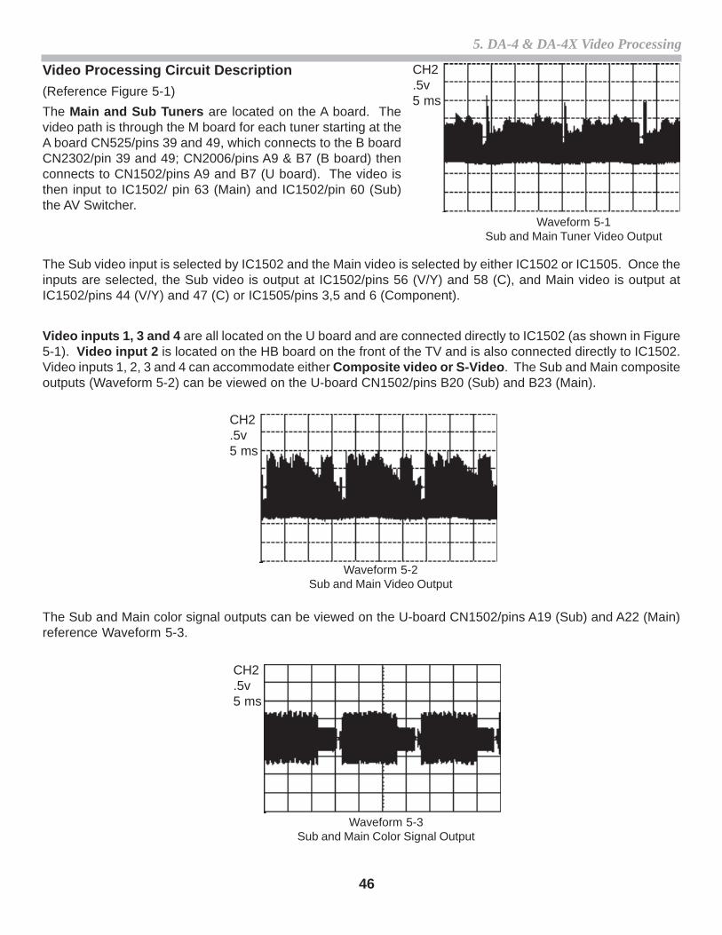
46
5. DA-4 & DA-4X Video Processing
Waveform 5-1Sub and Main Tuner Video Output
Waveform 5-3Sub and Main Color Signal Output
Waveform 5-2Sub and Main Video Output
CH2.5v5 ms
CH2.5v5 ms
CH2.5v5 ms
Video Processing Circuit Description(Reference Figure 5-1)
The Main and Sub Tuners are located on the A board. Thevideo path is through the M board for each tuner starting at theA board CN525/pins 39 and 49, which connects to the B boardCN2302/pin 39 and 49; CN2006/pins A9 & B7 (B board) thenconnects to CN1502/pins A9 and B7 (U board). The video isthen input to IC1502/ pin 63 (Main) and IC1502/pin 60 (Sub)the AV Switcher.
The Sub video input is selected by IC1502 and the Main video is selected by either IC1502 or IC1505. Once theinputs are selected, the Sub video is output at IC1502/pins 56 (V/Y) and 58 (C), and Main video is output atIC1502/pins 44 (V/Y) and 47 (C) or IC1505/pins 3,5 and 6 (Component).
Video inputs 1, 3 and 4 are all located on the U board and are connected directly to IC1502 (as shown in Figure5-1). Video input 2 is located on the HB board on the front of the TV and is also connected directly to IC1502.Video inputs 1, 2, 3 and 4 can accommodate either Composite video or S-Video. The Sub and Main compositeoutputs (Waveform 5-2) can be viewed on the U-board CN1502/pins B20 (Sub) and B23 (Main).
The Sub and Main color signal outputs can be viewed on the U-board CN1502/pins A19 (Sub) and A22 (Main)reference Waveform 5-3.
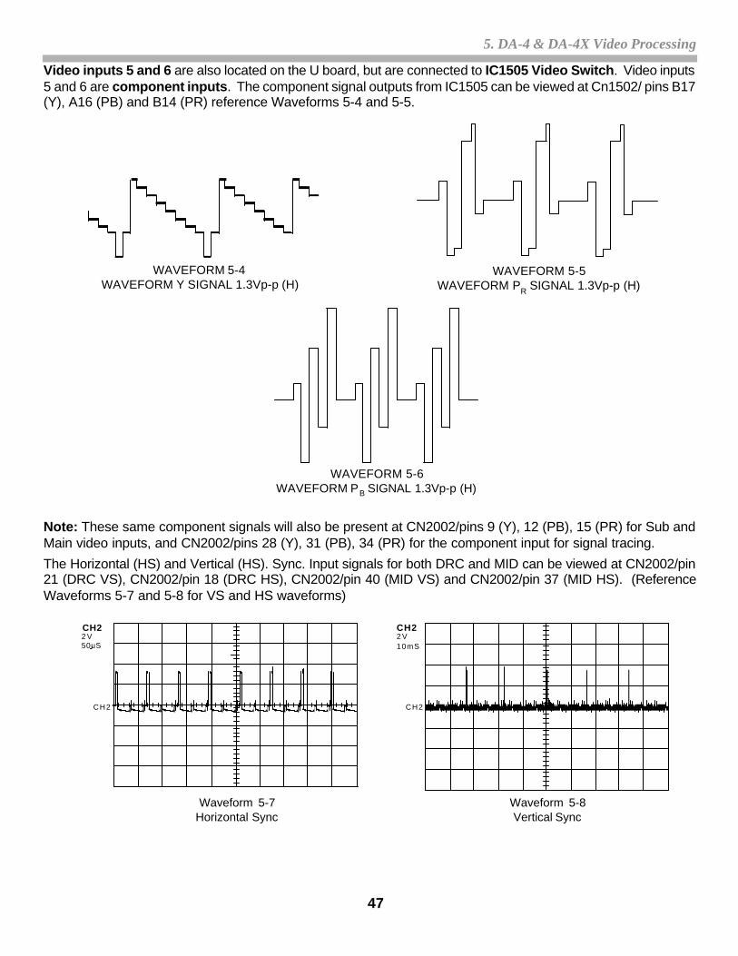
47
5. DA-4 & DA-4X Video Processing
Waveform 5-7Horizontal Sync
Waveform 5-8Vertical Sync
WAVEFORM 5-4WAVEFORM Y SIGNAL 1.3Vp-p (H)
WAVEFORM 5-5WAVEFORM PR SIGNAL 1.3Vp-p (H)
WAVEFORM 5-6WAVEFORM PB SIGNAL 1.3Vp-p (H)
CH22 V10mS
CH2
CH22 V50uS
CH2
Video inputs 5 and 6 are also located on the U board, but are connected to IC1505 Video Switch. Video inputs5 and 6 are component inputs. The component signal outputs from IC1505 can be viewed at Cn1502/ pins B17(Y), A16 (PB) and B14 (PR) reference Waveforms 5-4 and 5-5.
Note: These same component signals will also be present at CN2002/pins 9 (Y), 12 (PB), 15 (PR) for Sub andMain video inputs, and CN2002/pins 28 (Y), 31 (PB), 34 (PR) for the component input for signal tracing.
The Horizontal (HS) and Vertical (HS). Sync. Input signals for both DRC and MID can be viewed at CN2002/pin21 (DRC VS), CN2002/pin 18 (DRC HS), CN2002/pin 40 (MID VS) and CN2002/pin 37 (MID HS). (ReferenceWaveforms 5-7 and 5-8 for VS and HS waveforms)
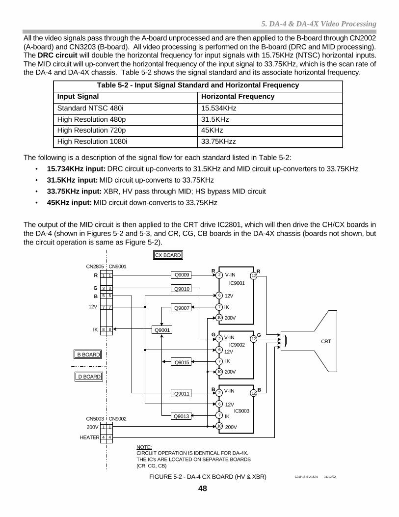
48
5. DA-4 & DA-4X Video Processing
5
7
8
3
1
4
1
2
6
7
10
2
6
7
10
2
6
7
10
Q9001
5
7
8
3
1
4
1
12
12
12
CRT
V-IN
12V
R
200V
IK
IC9001
IC9002
IC9003
V-IN
12V
IK
200V
V-IN
12V
IK
200V
G
B
R
G
B
Q9007
Q9009
Q9010
Q9011
Q9015
Q9013
200V
HEATER
12V
IK
R
G
B
CN9002CN5003
CN9001CN2805
D BOARD
B BOARD
CX BOARD
NOTE:CIRCUIT OPERATION IS IDENTICAL FOR DA-4X.THE IC's ARE LOCATED ON SEPARATE BOARDS(CR, CG, CB)
FIGURE 5-2 - DA-4 CX BOARD (HV & XBR) C31P15-5-2 1524 11/12/02
All the video signals pass through the A-board unprocessed and are then applied to the B-board through CN2002(A-board) and CN3203 (B-board). All video processing is performed on the B-board (DRC and MID processing).The DRC circuit will double the horizontal frequency for input signals with 15.75KHz (NTSC) horizontal inputs.The MID circuit will up-convert the horizontal frequency of the input signal to 33.75KHz, which is the scan rate ofthe DA-4 and DA-4X chassis. Table 5-2 shows the signal standard and its associate horizontal frequency.
Table 5-2 - Input Signal Standard and Horizontal Frequency
Input Signal Horizontal Frequency
Standard NTSC 480i 15.534KHz
High Resolution 480p 31.5KHz High Resolution 720p 45KHz
High Resolution 1080i 33.75KHzz
The following is a description of the signal flow for each standard listed in Table 5-2:
• 15.734KHz input: DRC circuit up-converts to 31.5KHz and MID circuit up-converters to 33.75KHz
• 31.5KHz input: MID circuit up-converts to 33.75KHz
• 33.75KHz input: XBR, HV pass through MID; HS bypass MID circuit
• 45KHz input: MID circuit down-converts to 33.75KHz
The output of the MID circuit is then applied to the CRT drive IC2801, which will then drive the CH/CX boards inthe DA-4 (shown in Figures 5-2 and 5-3, and CR, CG, CB boards in the DA-4X chassis (boards not shown, butthe circuit operation is same as Figure 5-2).
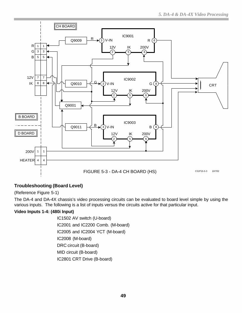
49
5. DA-4 & DA-4X Video Processing
IC90013
2 5 6
8V-IN
12V IK 200V
R
IC90023
2 5 6
8V-IN
12V IK 200V
G
IC90033
2 5 6
8V-IN
12V IK 200V
B
1
3
5
7
8
1
3
5
7
8
Q9009
Q9010
Q9011
Q9001
1
4
1
4
R
G
B
12V
IK
200V
HEATER
R
FIGURE 5-3 - DA-4 CH BOARD (HS) 10/7/02C31P15-5-3
B BOARD
D BOARD
CH BOARD
G
B
CRT
Troubleshooting (Board Level)(Reference Figure 5-1)
The DA-4 and DA-4X chassis’s video processing circuits can be evaluated to board level simple by using thevarious inputs. The following is a list of inputs versus the circuits active for that particular input.
Video Inputs 1-4: (480i Input)IC1502 AV switch (U-board)
IC2001 and IC2200 Comb. (M-board)
IC2005 and IC2004 YCT (M-board)
IC2008 (M-board)
DRC circuit (B-board)
MID circuit (B-board)
IC2801 CRT Drive (B-board)
50
5. DA-4 & DA-4X Video Processing
Video Inputs 5 and 6: (1080i Input)
IC1505 Video Switch (U-borad)
IC2006 Component I/F (M-board)
MID circuit (B-board)
IC2801 CRT Drive (B-board)
DVI Input
IC1505 Video Switch (M-board)
MID circuitIC2801 CRT Drive (B-board)
Memory Stick Input:
MID circuit (B-board)
IC2801 CRT Drive (B-board)
Note that by applying signals to the various inputs, complete circuits and boards can be bypassed to determineon which board the defective circuit is located. This is the most efficient way to troubleshoot the video processingcircuits because the M and B boards are not field repairable.
EXAMPLES:
(Reference Figure 5-1)
1) The Memory Stick Input will bypass the U and M boards.
2) The DVI Input will bypass the U board.
3) The Video 1-4 and Video 5-6 inputs can be used to isolate a defect to either IC1502 or IC1505.
Note: 480i will add the DRC circuit before the MID circuit.
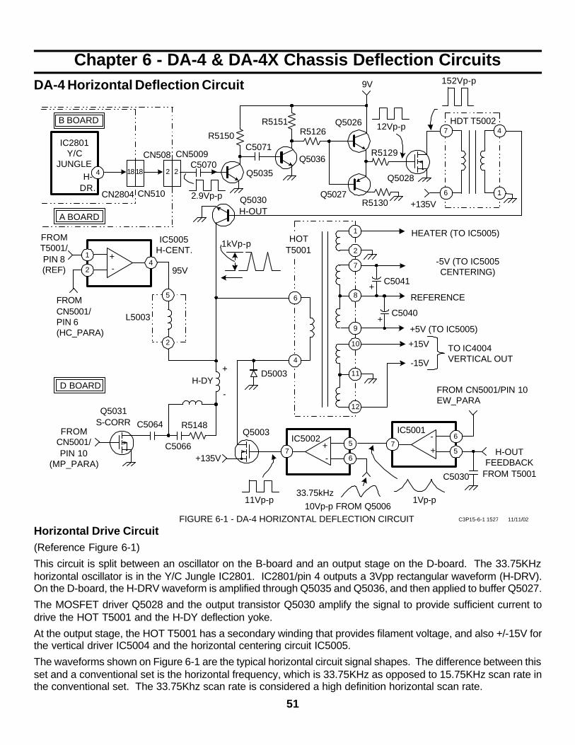
51
6. DA-4 & DA-4X Deflection Circuits
Chapter 6 - DA-4 & DA-4X Chassis Deflection CircuitsDA-4 Horizontal Deflection Circuit
FROMT5001/PIN 8(REF)
41
2
4 1818 2 2
IC2801Y/C
JUNGLE
7
6
4
1
6
4
7
9
8
2
1
10
12
11H-DY
75
6
76
5
2
5
H-OUTFEEDBACK
FROM T5001
FROM CN5001/PIN 10EW_PARA
FROMCN5001/PIN 6(HC_PARA)
IC5005H-CENT.
L5003
FROMCN5001/PIN 10
(MP_PARA)
Q5031S-CORR C5064
Q5030H-OUT
D5003
+135V
Q5003
H-DR.
R5150
R5151R5126
Q5026
Q5036
Q5035
Q5027R5130
9V
+135V
Q5028
1kVp-p HOTT5001
HEATER (TO IC5005)
-5V (TO IC5005CENTERING)
REFERENCE
+5V (TO IC5005)
+15V
-15V
+
+
HDT T5002
C5041
C5040
+-
-
++-
CN508 CN5009
CN510CN2804
B BOARD
A BOARD
D BOARD
IC5002IC5001
10Vp-p FROM Q50061Vp-p11Vp-p
12Vp-p
33.75kHz
FIGURE 6-1 - DA-4 HORIZONTAL DEFLECTION CIRCUIT C3P15-6-1 1527 11/11/02
152Vp-p
2.9Vp-p
C5066
R5148
TO IC4004VERTICAL OUT
95V
+
-
R5129C5070
C5071
C5030
Horizontal Drive Circuit(Reference Figure 6-1)
This circuit is split between an oscillator on the B-board and an output stage on the D-board. The 33.75KHzhorizontal oscillator is in the Y/C Jungle IC2801. IC2801/pin 4 outputs a 3Vpp rectangular waveform (H-DRV).On the D-board, the H-DRV waveform is amplified through Q5035 and Q5036, and then applied to buffer Q5027.
The MOSFET driver Q5028 and the output transistor Q5030 amplify the signal to provide sufficient current todrive the HOT T5001 and the H-DY deflection yoke.
At the output stage, the HOT T5001 has a secondary winding that provides filament voltage, and also +/-15V forthe vertical driver IC5004 and the horizontal centering circuit IC5005.
The waveforms shown on Figure 6-1 are the typical horizontal circuit signal shapes. The difference between thisset and a conventional set is the horizontal frequency, which is 33.75KHz as opposed to 15.75KHz scan rate inthe conventional set. The 33.75Khz scan rate is considered a high definition horizontal scan rate.
52
6. DA-4 & DA-4X Deflection Circuits
PWM Circuit(Reference Figure 6-1)The PWM circuit (Q5003) has two functions. First, it provides a regulated 102Vdc output for the horizontaloutput transistor Q5030. Second, it compensates for horizontal pincushion affect and keeps the picture verticaledges straight.
Regulator
The PWM circuit regulates +135Vdc from the power supply down to +102Vdc. Horizontal pulses from IC8004/pin 1 (not shown in Figure 6-1) in the HV power supply section drive Q5003. The pulses are amplified and outputto the HOT T5001/pin 4. To control the output voltage, the output is sampled and used to change the pulse widthof the H drive pulses. These changes regulate the output voltage to +102Vdc at T5001/pin 4.
Pincushion Correction
If the PWM output voltage at T5001/pin 4 were changed, the horizontal picture size would vary accordingly. Avertical pincushion signal is produced at IC2801/pin 11 (not shown) and is applied to the PWM circuit to increasethe picture width and compensate for the pincushion distortion.
The EW_PARA parabola signal form CN5001/pin 1 (D-board) is first applied to IC5001/pin 6 and output onIC5001/pin 7, and then applied to IC5002/pin 5. The parabola signal at IC5002/pin 5 is compared to the sawtoothwaveform at IC5002/pin 6. This comparison causes the PWM signal at the output IC5002/pin 7 to vary in pulsewidth. The change in pulse width causes more or less voltage to be applied to the horizontal output Q5030collector during the vertical scan down the CRT. This varying voltage causes a varying current to be applied tothe H-DY. Current is gradually increased as the beam scans down until the current is maximum at the center ofthe CRT where the pincushion distortion is the most extreme. The result is a good, straight line scan down bothsides of the CRT.
Heater Voltage
The filament voltage is applied when the horizontal oscillator signal produces horizontal sweep. The horizontaloutput transformer T5001/pin 1 outputs 7.7Vdc when power is ON. This voltage is regulated to 6.1Vdc byIC5006 to become the main filament voltage.H-Centering and S-Correction
Also shown in Figure 6-1 is the H-Centering circuit. This circuit applies a small dc-offset to the H-DY to keep thepicture centered on the CRT. This function is performed dynamically through the service mode by varying theparabola waveform at CN5001/pin 6 (HC_PARA). The HC_PARA after is applied to IC5005/pin 2 and a dc-offsetis produce at IC5005/pin 4.
The S-Correction circuit is used to correct for the slight “S” shaped distortion that appears in each horizontalline. Once again this function is performed dynamically through the service mode by varying the parabolawaveform at CN5001/pin 10 (MP_PARA).
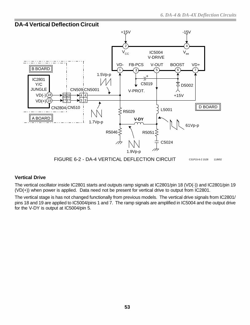
53
6. DA-4 & DA-4X Deflection Circuits
18 2828 4 4
IC2801Y/C
JUNGLEVD(-)
CN509
CN510CN2804
B BOARD
A BOARD
2727 3 319
CN5001
VD(+)
1 3 5 6 7
2 4
FB-PCS V-OUT BOOST VD+VD-
VCC VeeIC5004V-DRIVE
V-PROT.+15V
C5024
R5051
R5029
R5046
V-DY
L5001
61Vp-p
1.9Vp-p
1.7Vp-p
1.5Vp-p
C5019
+
+15V -15V
FIGURE 6-2 - DA-4 VERTICAL DEFLECTION CIRCUIT C31P15-6-2 1528 11/8/02
D BOARD
D5002
DA-4 Vertical Deflection Circuit
Vertical DriveThe vertical oscillator inside IC2801 starts and outputs ramp signals at IC2801/pin 18 (VD(-)) and IC2801/pin 19(VD(+)) when power is applied. Data need not be present for vertical drive to output from IC2801.
The vertical stage is has not changed functionally from previous models. The vertical drive signals from IC2801/pins 18 and 19 are applied to IC5004/pins 1 and 7. The ramp signals are amplified in IC5004 and the output drivefor the V-DY is output at IC5004/pin 5.
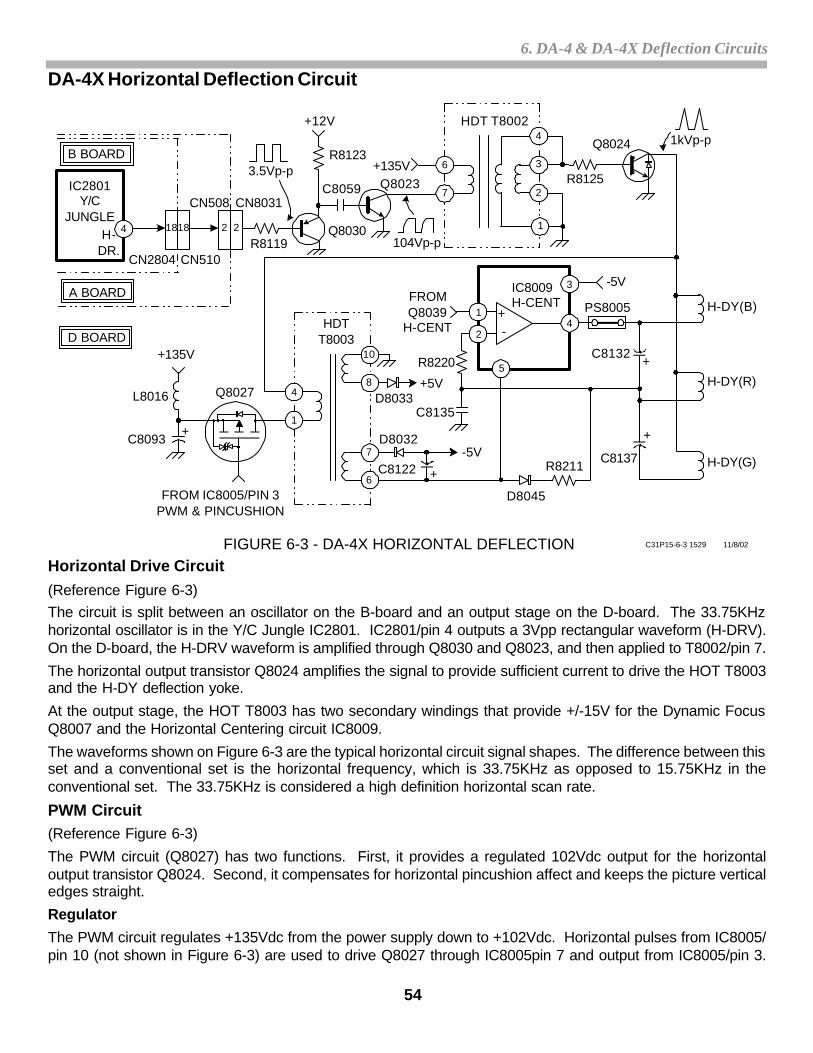
54
6. DA-4 & DA-4X Deflection Circuits
4 1818 2 2
IC2801Y/C
JUNGLE
6
7
4
1H-
DR.
HDT T8002
CN508 CN8031
CN510CN2804
B BOARD
A BOARD
3
2
41
2
+-
+
+
1kVp-p
104Vp-p
3.5Vp-p
Q8027L8016
+135V
+C8093
FROM IC8005/PIN 3PWM & PINCUSHION
FROMQ8039
H-CENT
R8220
C8135
PS8005
C8137
C8132
R8125
Q8024
+135V
+12V
R8119Q8030
Q8023
IC8009H-CENT H-DY(B)
H-DY(R)
H-DY(G)
3 -5V
FIGURE 6-3 - DA-4X HORIZONTAL DEFLECTION C31P15-6-3 1529 11/8/02
1
4
-5V7
8
6 +
D8033
D8032
C8122
HDTT8003
+5V
10
D BOARD
5
D8045
R8211
C8059
R8123
DA-4X Horizontal Deflection Circuit
Horizontal Drive Circuit(Reference Figure 6-3)The circuit is split between an oscillator on the B-board and an output stage on the D-board. The 33.75KHzhorizontal oscillator is in the Y/C Jungle IC2801. IC2801/pin 4 outputs a 3Vpp rectangular waveform (H-DRV).On the D-board, the H-DRV waveform is amplified through Q8030 and Q8023, and then applied to T8002/pin 7.
The horizontal output transistor Q8024 amplifies the signal to provide sufficient current to drive the HOT T8003and the H-DY deflection yoke.
At the output stage, the HOT T8003 has two secondary windings that provide +/-15V for the Dynamic FocusQ8007 and the Horizontal Centering circuit IC8009.
The waveforms shown on Figure 6-3 are the typical horizontal circuit signal shapes. The difference between thisset and a conventional set is the horizontal frequency, which is 33.75KHz as opposed to 15.75KHz in theconventional set. The 33.75KHz is considered a high definition horizontal scan rate.
PWM Circuit(Reference Figure 6-3)
The PWM circuit (Q8027) has two functions. First, it provides a regulated 102Vdc output for the horizontaloutput transistor Q8024. Second, it compensates for horizontal pincushion affect and keeps the picture verticaledges straight.
Regulator
The PWM circuit regulates +135Vdc from the power supply down to +102Vdc. Horizontal pulses from IC8005/pin 10 (not shown in Figure 6-3) are used to drive Q8027 through IC8005pin 7 and output from IC8005/pin 3.
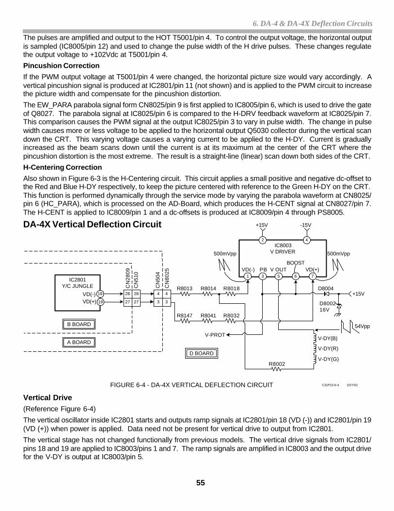
55
6. DA-4 & DA-4X Deflection Circuits
IC2801Y/C JUNGLE
18
19
VD(-)VD(+)
B BOARD
28
27
28
27
CN
2809
CN
510
CN
504
CN
8025
A BOARD
IC8003V DRIVER
1VD(-)
3PB V OUT
6 7VD(+)
BOOST
4
3
4
3
R8013 R8014 R8018
R8147 R8041 R8032
5
R8002
V-PROT
D8004
D800216V
+15V
V-DY(B)
V-DY(R)
V-DY(G)
FIGURE 6-4 - DA-4X VERTICAL DEFLECTION CIRCUIT 10/7/02C31P15-6-4
500mVpp
54Vpp
500mVpp
2 4
+15V -15V
D BOARD
The pulses are amplified and output to the HOT T5001/pin 4. To control the output voltage, the horizontal outputis sampled (IC8005/pin 12) and used to change the pulse width of the H drive pulses. These changes regulatethe output voltage to +102Vdc at T5001/pin 4.
Pincushion Correction
If the PWM output voltage at T5001/pin 4 were changed, the horizontal picture size would vary accordingly. Avertical pincushion signal is produced at IC2801/pin 11 (not shown) and is applied to the PWM circuit to increasethe picture width and compensate for the pincushion distortion.
The EW_PARA parabola signal form CN8025/pin 9 is first applied to IC8005/pin 6, which is used to drive the gateof Q8027. The parabola signal at IC8025/pin 6 is compared to the H-DRV feedback waveform at IC8025/pin 7.This comparison causes the PWM signal at the output IC8025/pin 3 to vary in pulse width. The change in pulsewidth causes more or less voltage to be applied to the horizontal output Q5030 collector during the vertical scandown the CRT. This varying voltage causes a varying current to be applied to the H-DY. Current is graduallyincreased as the beam scans down until the current is at its maximum at the center of the CRT where thepincushion distortion is the most extreme. The result is a straight-line (linear) scan down both sides of the CRT.
H-Centering Correction
Also shown in Figure 6-3 is the H-Centering circuit. This circuit applies a small positive and negative dc-offset tothe Red and Blue H-DY respectively, to keep the picture centered with reference to the Green H-DY on the CRT.This function is performed dynamically through the service mode by varying the parabola waveform at CN8025/pin 6 (HC_PARA), which is processed on the AD-Board, which produces the H-CENT signal at CN8027/pin 7.The H-CENT is applied to IC8009/pin 1 and a dc-offsets is produced at IC8009/pin 4 through PS8005.
DA-4X Vertical Deflection Circuit
Vertical Drive(Reference Figure 6-4)
The vertical oscillator inside IC2801 starts and outputs ramp signals at IC2801/pin 18 (VD (-)) and IC2801/pin 19(VD (+)) when power is applied. Data need not be present for vertical drive to output from IC2801.
The vertical stage has not changed functionally from previous models. The vertical drive signals from IC2801/pins 18 and 19 are applied to IC8003/pins 1 and 7. The ramp signals are amplified in IC8003 and the output drivefor the V-DY is output at IC8003/pin 5.
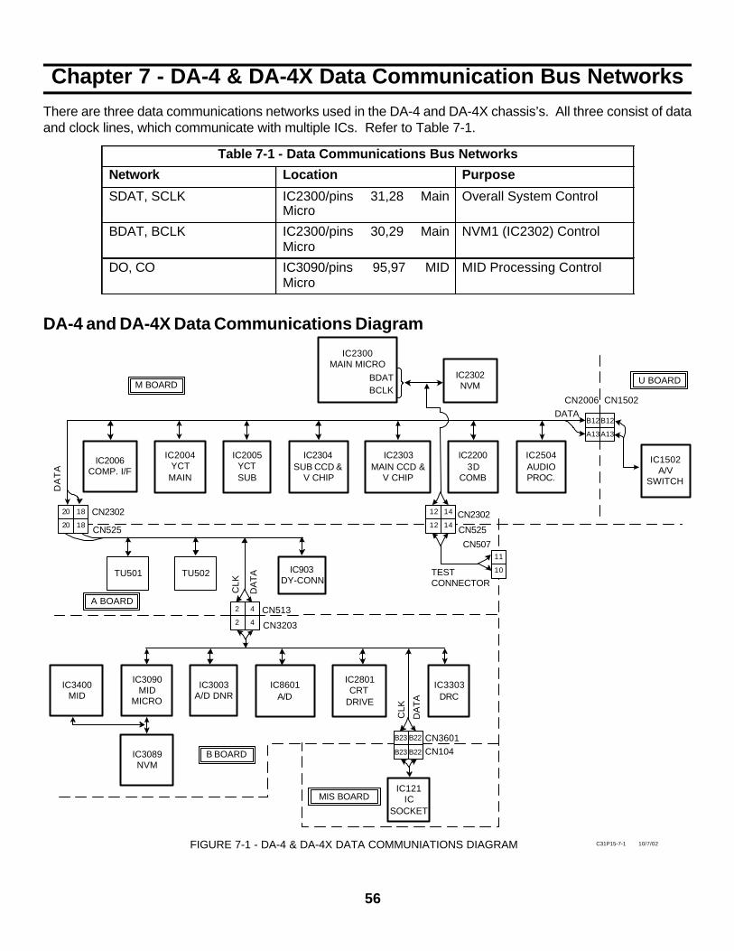
56
7. DA-4 & DA-4X Data Communication Bus Networks
Chapter 7 - DA-4 & DA-4X Data Communication Bus Networks
IC2006COMP. I/F
IC2004YCT
MAIN
IC2005YCTSUB
IC2304SUB CCD &
V CHIP
IC2303MAIN CCD &
V CHIP
IC22003D
COMB
IC2504AUDIOPROC.
20
20
18
18
B12
A13
B12
A13
12
12
14
14
IC2300MAIN MICRO
IC2302NVM
TU501 TU502 IC903DY-CONN
M BOARDBDATBCLK
CN2302
CN525
CN2302
CN525
2
2
4
4
A BOARDCN513
CN3203
IC3400MID
IC3090MID
MICRO
IC3003A/D DNR
IC8601A/D
IC2801CRT
DRIVE
IC3303DRC
IC1502A/V
SWITCH
U BOARD
CN507
TESTCONNECTOR
CN2006 CN1502
IC3089NVM
B BOARD
B23
B23
B22
B22
CN3601CN104
IC121IC
SOCKET
MIS BOARD
10/7/02C31P15-7-1FIGURE 7-1 - DA-4 & DA-4X DATA COMMUNIATIONS DIAGRAM
DA
TA
CLK
DA
TA
11
10
DA
TA
CLK
DATA
There are three data communications networks used in the DA-4 and DA-4X chassis’s. All three consist of dataand clock lines, which communicate with multiple ICs. Refer to Table 7-1.
Table 7-1 - Data Communications Bus Networks
Network Location Purpose
SDAT, SCLK IC2300/pins 31,28 Main Micro
Overall System Control
BDAT, BCLK IC2300/pins 30,29 Main Micro
NVM1 (IC2302) Control
DO, CO IC3090/pins 95,97 MID Micro
MID Processing Control
DA-4 and DA-4X Data Communications Diagram
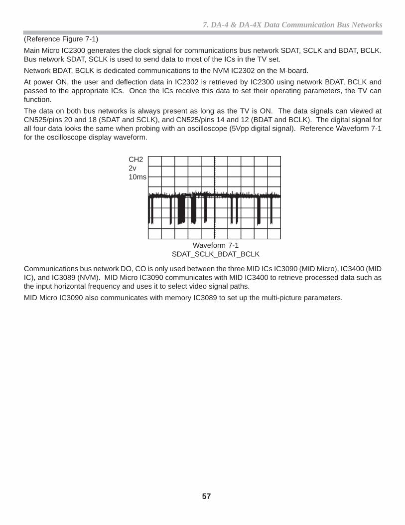
57
7. DA-4 & DA-4X Data Communication Bus Networks
Waveform 7-1SDAT_SCLK_BDAT_BCLK
CH22v10ms
(Reference Figure 7-1)
Main Micro IC2300 generates the clock signal for communications bus network SDAT, SCLK and BDAT, BCLK.Bus network SDAT, SCLK is used to send data to most of the ICs in the TV set.
Network BDAT, BCLK is dedicated communications to the NVM IC2302 on the M-board.
At power ON, the user and deflection data in IC2302 is retrieved by IC2300 using network BDAT, BCLK andpassed to the appropriate ICs. Once the ICs receive this data to set their operating parameters, the TV canfunction.
The data on both bus networks is always present as long as the TV is ON. The data signals can viewed atCN525/pins 20 and 18 (SDAT and SCLK), and CN525/pins 14 and 12 (BDAT and BCLK). The digital signal forall four data looks the same when probing with an oscilloscope (5Vpp digital signal). Reference Waveform 7-1for the oscilloscope display waveform.
Communications bus network DO, CO is only used between the three MID ICs IC3090 (MID Micro), IC3400 (MIDIC), and IC3089 (NVM). MID Micro IC3090 communicates with MID IC3400 to retrieve processed data such asthe input horizontal frequency and uses it to select video signal paths.
MID Micro IC3090 also communicates with memory IC3089 to set up the multi-picture parameters.
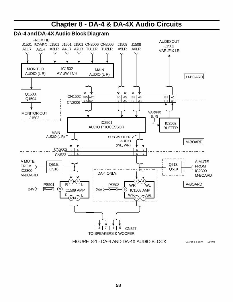
58
8. DA-4 & DA-4X Audio Circuits
Chapter 8 - DA-4 & DA-4X Audio Circuits
IC2501AUDIO PROCESSOR
3
B25 A25 B5 A5 B3 A3 B1 A1B25 A25 B5 A5 B3 A3 B1 A1
2 4 6 72 4 6 7
VAR/FIX(L R)
IC2502BUFFER
MONITORAUDIO (L R)
MAINAUDIO (L R)
MAINAUDIO (L R)
IC1502AV SWITCH
J1501A1LR
FROM HBBOARDA2LR
J1501A3LR
J1501A4LR
J1501A7LR
CN2006TU1LR
CN2006TU2LR
J1509A5LR
J1508A6LR
AUDIO OUTJ1502
VAR./FIX LR
Q1503,Q1504
MONITOR OUTJ1502
2 4 2 4
IC1509 AMPWLR WRL
R L712 712
IC1508 AMP
7 1 5
Q515,Q516
Q518,Q519
9 9PS501 PS502
24V 24V
A MUTEFROMIC2300M-BOARD
A MUTEFROMIC2300M-BOARD DA-4 ONLY
CN2002CN523
WR WL
CN1502
CN2006
CN527
M-BOARD
U-BOARD
A-BOARD
FIGURE 8-1 - DA-4 AND DA-4X AUDIO BLOCK
TO SPEAKERS & WOOFER
C31P15-8-1 1530 11/4/02
SUB WOOFERAUDIO
(WL, WR)
DA-4 and DA-4X Audio Block Diagram
59
8. DA-4 & DA-4X Audio Circuits
(Reference Figure 8-1)
IC1502 is an Audio/Video Switch (located on the U-board), which selects both audio and video using the I2C busfrom Main Micro IC2300 (not shown). The following audio inputs are available to IC1502:
• Audio 1 – 4
• Audio 7
• TU1 & 2
The selected audio is then sent to the M-board through CN1502/pins B25 & A25 (U-board) and CN2006/pins B25& A25 (M-board), and applied to the audio processor IC2501. Audio inputs 5 & 6 from the U-board are applieddirectly to the audio processor IC2501 (U-board) through CN1502/pins B5, A5, B3 and A3 (U-Board), and CN2006/pins B5, A5, B3 and A3 (U-Board).
The Monitor L/R output also is output from the AV Switch IC1502, applied to Q1504 (buffer) and Q1503 (buffer),and then to J1503.
The audio processor IC2501 takes the main audio input and produces a main L/R output and sub-woofer WL/WR output (IC2501 also produces the Steady Sound feature). These outputs are then passed to the A-boardthrough CN2002/pins 2, 4, 6 and 7 (M-board) and CN523/pins 2, 4, 6 and 7 (A-board). Next they are applied tothe audio amplifies IC509/pins 2 & 4 (Midrange) and IC1508/pins 2 and 4 (Woofer). Note: IC508 is not used inthe DA-4X chassis (projection set). The low frequencies are enhanced in the protection set used theDAC Speaker System. The DAC system uses the Midrange speakers TV cabinet as a low frequencychamber system.
The VAR/FIX L/R audio is output from Audio Processor IC2501. Audio passes through buffer IC2502 and thento CN2006/pins B1 and A1 (M-board), CN1502/pins B1 and A1, and is finally output at J1502.
Speaker outputs can be viewed at CN527/pins 3, 7, 1 and 5.
Mute transistor Q515, 516, 518 and 519 are activated when the MUTE or Channel buttons are pressed on theremote controller (audio is mute between channels when changing channels). The A-MUTE line will go High,and the transistor will turn ON and send the audio to ground muting the audio output.
C31P151102 11/15/02
, HDTV and Memory Stick are trademarks of Sony Electronics
©2002 Sony Electronics Inc.EMCS - A Service Company
1 Sony DrivePark Ridge, New Jersey 07656
Reproduction in whole or part without written permission is prohibited. All rights reserved