Embed Size (px)
Citation preview

TRANSPARENT THIN FILM HEATERS
BASED ON SILVER NANOWIRE NETWORKS
A THESIS SUBMITTED TO
THE GRADUATE SCHOOL OF NATURAL AND APPLIED SCIENCES
OF
MIDDLE EAST TECHNICAL UNIVERSITY
BY
ORÇUN ERGÜN
IN PARTIAL FULFILLMENT OF THE REQUIREMENTS
FOR
THE DEGREE OF MASTER OF SCIENCE
IN
METALLURGICAL AND MATERIALS ENGINEERING DEPARTMENT
AUGUST 2015


Approval of the thesis:
TRANSPARENT THIN FILM HEATERS
BASED ON SILVER NANOWIRE NETWORKS
Submitted by ORÇUN ERGÜN in partial fulfillment of the requirements for the
degree of Master of Science in Metallurgical and Materials Engineering
Department, Middle East Technical University by,
Prof. Dr. Gülbin Dural Ünver ____________
Dean, Graduate School of Natural and Applied Sciences
Prof. Dr. C. Hakan Gür ____________
Head of Department, Metallurgical and Materials Eng.Dept., METU
Assoc. Prof. Dr. Hüsnü Emrah Ünalan ____________
Supervisor, Metallurgical and Materials Eng.Dept., METU
Examining Committee Members:
Prof. Dr. Raşit Turan _____________________
Physics Dept., METU
Assoc. Prof. Dr. Emren Nalbant Esentürk _____________________
Chemistry Dept., METU
Assoc. Prof. Dr. Abdullah Ceylan _____________________
Physics Eng. Dept., Hacettepe Univ.
Assoc. Prof. Dr. Yunus Eren Kalay _____________________
Metallurgical and Materials Eng. Dept., METU
Assoc. Prof. Dr. Hüsnü Emrah Ünalan _____________________
Metallurgical and Materials Eng. Dept., METU
Date: 24. 08. 2015
iv
I hereby declare that all information in this document has been obtained and
presented in accordance with academic rules and ethical conduct. I also declare
that, as required by these rules and conduct, I have fully cited and referenced
all material and results that are not original to this work.
Name, Last Name: Orçun ERGÜN
Signature:

v
ABSTRACT
TRANSPARENT THIN FILM HEATERS
BASED ON SILVER NANOWIRE NETWORKS
Ergün, Orçun
M. S., Department of Metallurgical and Materials Engineering
Supervisor: Assoc. Prof. Dr. Hüsnü Emrah Ünalan
August 2015, 71 pages
Transparent thin film heaters are used in various de-fogging and de-icing
applications because of their ability to convert electrical energy to thermal energy
while allowing to transmit solar light through a surface. Indium tin oxide (ITO) is
the conventional transparent conducting material used in transparent thin film
heaters. However, due to scarcity of indium and its increasing prices worldwide,
coupled with the inflexibility of ITO, alternative materials are being investigated.
Silver nanowire networks have a great potential to be used as transparent thermal
thin film heaters because bulk silver has the highest electrical conductivity among
other metals, which result in low sheet resistances. Moreover, silver nanowire thin
film networks demonstrate high optical transparency with low sheet resistance.
Diameter of silver nanowires are in the order of few tens of nanometers, which
confines electrons to travel through one dimension that result in high thermal
performance due to Joule heating. In addition, silver nanowire based transparent thin
film heaters can be made flexible on polymeric substrates.

vi
In this thesis, silver nanowire based transparent thin film heaters were fabricated on
quartz, soda lime silicate glass, polyethylene terephthalate (PET) substrates.
Nanowire networks were deposited through simple spray coating method. Thermal
performance as well as optoelectronic characteristics of the networks were
determined. It is concluded that silver nanowire based transparent thin film heaters
demonstrate high thermal performance coupled with high optical transmittance.
Keywords: transparent thin film heaters, silver nanowires, spray coating.
vii
ÖZ
GÜMÜŞ NANOTEL İNCE FİLMLER İLE
ŞEFFAF ISITICILAR
Ergün, Orçun
Yüksek Lisans, Metalürji ve Malzeme Mühendisliği Bölümü
Tez Yöneticisi: Doç. Dr. Hüsnü Emrah Ünalan
Ağustos 2015, 71 sayfa
Şeffaf ince film ısıtıcılar, bir yüzeyden güneş ışığının geçmesine izin verirken bu
yüzeyde elektrik enerjisini ısıl enerjiye dönüştürebilme özelliklerinden dolayı pek
çok buğu ve buz giderme uygulmasında kullanılırlar. İndiyum kalay oksit (ITO), bu
amaçla şeffaf ince film ısıtıcılarda en çok kullanılan şeffaf elektriksel iletken
malzemedir. Ancak, indiyumun azlığı ve dünya çapında artan fiyatları, ITO’nun
esnek olmama özelliğiyle birleştiğinden alternatif malzemeler araştırılmaktadır.
Gümüşün diğer metaller arasında en yüksek elektriksel iletkenliğe ve bu nedenle
düşük yüzey dirençlerine sahip olması nedeniyle, gümüş nanoteller şeffaf ince film
ısıtıcı olarak kullanılmada yüksek bir potansiyele sahiptir. Buna ek olarak, Gümüş
nanotel ince filmler düşük yüzey direnciyle birlikte yüksek optik geçirgenlik
sergiler. Gümüş nanotellerin bir kaç on nanometre olan çapları, elektronları bir
boyuta hapsederek ilerlemelerine ve Joule ısınmasıyla yüksek ısıtma performansı
sergilemelerine yol açar. Buna ek olarak, gümüş nanotelden yapılı ince film
ısıtıcılar, polimerik alttaşlar üzerinde esnek özelliğe sahip olarak üretilebilir.

viii
Bu tez çalışmasında, gümüş nanotel ince filmlerden yapılı şeffaf ısıtıcılar, kuvartz,
silika camı ve polietilen terefitalat (PET) alttaşları üzerinde üretildi. Nanotel ağları
sprey yöntemiyle kaplandı. Nanotel ağlarının ısıl performansı, optoelektronik
karakteristikleriyle birlikte saptandı. Gümüş nanotel ince filmlerden yapılı şeffaf
ısıtıcıların yüksek optik geçirgenlikle birlikte yüksek ısıl performansa sahip olduğu
sonucuna varılmıştır.
Anahtar Kelimeler: şeffaf ince film ısıtıcılar, gümüş nanoteller, sprey kaplama.

ix
To the memory of my beloved grandfather, Şerif Ali ERGÜN

x
ACKNOWLEDGEMENTS
I would like to express my gratitude to my supervisor Assoc. Prof. Dr. Hüsnü Emrah
ÜNALAN, for his guidance and encouragement during my studies. He is a true
inspiration as a high achiever young scientist.
Thanks to Şahin COŞKUN for preparing silver nanowires and transparent film
heaters. Without his invaluable help, solid guidance and patience with me, this
thesis would have never been completed.
I also would like to express my gratitude to my employer, ASELSAN A.Ş. and
“Radar, Electronic Warfare and Intelligence Systems” Sector’s head Oğuz ŞENER,
my director Şebnem SAYGINER and my manager Ali LAFCI for allowing me to
pursue my master’s degree, for their guidance in my academic endeavors and for
allowing me to use thermal measurement equipment for this research. We would
like to acknowledge the partial financial support provided by Arçelik A.Ş.
Murat MUTLUOL’s and Hüseyin YURDAKUL’s help in preparing TTFH samples,
Halil İbrahim ATASOY’s help in IR thermal camera measurements, Uğur ETİZ and
Murat PARLAK’s help in providing thermal measurement equipment, Selçuk
ÖKSÜZ’s help in measurement setup preparation are all greatly appreciated.
I sincerely thank my office mate Burcu AKSOY. I learned a lot from her point of
view in my scientific studies, in work-related topics and in my personal life. The
time we shared together has been so much fun and full of unforgettable moments.
She is a wonderful partner.

xi
Special thanks to Zeynep KARACA for her support during my studies, which is
kindly appreciated. I want to thank Elif Selen YÜCEL for her guidance during
preparation of my thesis. Her kind attitude and smiling face at the workplace is
always admired.
I thank Ali Sina ÖNDER, Erkut AYKUTLUĞ and Gökhan METAN for being with
me at hard times and sharing my happy moments even if they are at the other side of
the globe. They are like real brothers.
I would like to thank my grandmothers, my dear aunt Neshun KAVUTÇU, my
uncles, Zatiye Abla, Önalp, Çebi & Taşbaşlı families for a loving and supportive
family environment.
I thank my fabulous parents for their belief in me and for their support through all
my life. What I achieve belong to them. Their love and encouragement made this
thesis possible.
Thanks to İdil for being the greatest sister in the world and my undisclosed best
friend. Her strength to hold on under the most challenging conditions coupled with
her fun attitude towards life has been and will always be an inspiration during my
career and personal life.
And lastly, I deeply thank all people whose mission is to encourage others to follow
their dreams and passions. One of them is William Ernest Henley, whose words in
his famous poem “Invictus” give me the strength to pursue my dreams from now on
with an increasing and everlasting courage that stands against any fear:
“…It matters not how strait the gate,
How charged with punishments the scroll,
I am the master of my fate:
I am the captain of my soul.”

xii
TABLE OF CONTENTS
ABSTRACT................................................................................................................v
ÖZ.............................. ................................................................................................vii
ACKNOWLEDGEMENTS........................................................................................x
TABLE OF CONTENTS..........................................................................................xii
LIST OF FIGURES...................................................................................................xv
LIST OF TABLES.................................................................................................xviii
LIST OF ABBREVIATIONS..................................................................................xix
CHAPTERS
1. INTRODUCTION
1.1. Motivation for the Study...........................................................................1
1.2. Transparent Conducting Materials Used in Transparent Thin Film
Heaters ...……………………..………….…………………..........................4
1.2.1. Metal Oxides........................................................................................10
1.2.1.1. Indium Tin Oxide (ITO)................................................................12
1.2.1.2. Fluorine Doped Tin Oxide (FTO).…...……………….….……….15
1.2.1.3. Zinc Oxide (ZnO)…...…………………………..…………………15
1.2.2. Carbon Nanotubes (CNTs)...............………….….…………………16
1.2.3. Graphene…………………...……..……………….…………………17
1.2.4. Metallic Nanowires……………..……………………………………18
1.2.4.1. Silver Nanowires (Ag NWs).…………………………………….19
1.2.4.2. Gold Nanowires (Au NWs)……………………...……………...…19
1.2.5. Hybrid Materials…………………..……………….………..……....20
1.3. Silver Nanowire Thin Films…………….………………..…...…….....20
1.3.1. Percolation Theory and Optoelectronic Properties of Nanowires….20
1.3.2. Joule Heating Mechanism of Nanowire Networks ………………….22
xiii
1.3.3. Failure Mechanism of Silver Nanowire Networks due to Joule
Heating ……………………..……………...................................................24
1.4. Ag NW Synthesis by the Polyol Method ……………………………...24
1.5. Ag NW Transparent Thin Film Heater Fabrication by Spray Coating
……………………………..………………………………………...….......28
2. EXPERIMENTAL………...………………………………………………….….31
2.1. Networks of Ag NWs for the Fabrication of TTFHs……………..…....31
2.1.1. Ag NWs Synthesis………………………………………………..….31
2.1.2. Deposition of Ag NW Thin Films onto Various Substrates by Spray
Coating……..………………………………..…………..….………………33
2.1.3. Physical Vapor Deposition of Ag Contacts on Ag NW Networks..…34
2.1.4. Electrical Wiring and Cable Bonding ………...….……………....…36
2.2. Infrared Imaging and Thermal Mapping for the TTFH Devices….…37
2.3. Thermal Measurements under Bias….…….……………….………….38
2.4. Scanning Electron Microscopy Imaging………………………..….…..39
2.5. Sheet Resistance Measurements…………………………..…...………40
2.6. Transparency Measurements………………...…………………....…...40
3. RESULTS AND DISCUSSION………………….…...…………….………...…41
3.1. Effect of Contact Geometry……………...…………………………..41
3.1.1. IR Thermal Camera Temperature Mappings…..……..………….…41
3.2. Effect of Ag NW Thin Film Density…………………………..….44
3.2.1. SEM Images………………...………………………………….….…44
3.2.2. Transparency, Sheet Resistance and Nanowire Density…….….…..45
3.2.3. Thermal Measurements Under Bias……………………….………..46
3.3. Effect of Bias Voltage…..……………….…………………………….48
3.3.1. Effect of Incremental Increase in Voltage Applied……………..…51
3.4. Effect of Repetitive Heating and Cooling Cycles ……………….…...53
3.5. Long Term Stability of TTFHs................................……………….…..55
3.6. Reproducibility of the TTFH Characteristics …………………………56
3.7. Flexibility……………………...………………………………...…..…58

xiv
4. CONCLUSIONS AND FUTURE WORK…..…………….…………………….59
4.1. Summary of the Work……………………………………….…59
4.2. Future Work………………………………………………..…..61
REFERENCES……………………………………………………………………..63

xv
LIST OF FIGURES
Figure 1.1. A flexible transparent conducting Ag NW thin film on a polymeric
substrate.......................................................................................................................2
Figure 1.2. A commercial Kapton flexible thin film heater.......................................2
Figure 1.3. a) A silver nanowire based touch-screen panel (Cambrios ClearOhm), b)
Structure of a touch-screen panel................................................................................5
Figure 1.4. Examples of various TCOs...................................................................11
Figure 1.5. Thermal response of solution-processed ITO nanoparticles based
TTFHs at various bias conditions..............................................................................14
Figure 1.6. Thermal response characteristics of ITO nanoparticle paste based
microheaters at various bias conditions.....................................................................15
Figure 1.7. Heating performance of MWCNT sheet heaters....................................17
Figure 1.8. Percolation theory explained through conductivity as a function of
percentage of NW projection area to the sample area..........................................21
Figure 1.9. Transparency versus sheet resistance for various TCMs.......................22
Figure 1.10. A schematic of the synthesis mechanism of Ag NWs via solution based
polyol process............................................................................................................27
Figure 2.1. Ethanolic solution of Ag NWs following purification..........................32
Figure 2.2. Spray coating of Ag NWs onto substrates.............................................33
Figure 2.3. A photo of (a) Ag NW thin film coated on quartz sample, (b) optical
microscope image of this film..................................................................................34
Figure 2.4. Optical images of the interface between Ag NWs and Ag thin films
showing (a) a succesful wetting and (b) a failed wetting ........................................35
Figure 2.5. Dimensions of substrate and Ag contacts utilized in this work.............36
Figure 2.6. A photo showing the final structure of the fabricated TTFHs in this
work...........................................................................................................................36

xvi
Figure 2.7. Thermal mapping in IR thermal camera setup.......................................37
Figure 2.8. Thermal measurement setup utilized in this work...............................38
Figure 2.9. A photo showing how the temperature measurements were taken via
thermocouples............................................................................................................39
Figure 2.10. Two probe setup used for the measurement of sheet resistances of the
thin films....................................................................................................................40
Figure 3.1. Thermal camera images showing the effect of contact geometry on
temperature distribution.............................................................................................42
Figure 3.2. Optical microscope images of Ag NW thin films at the contact interface
in parallel contact geometry (a) before and (b) after bias voltage application.......43
Figure 3.3 SEM images of Ag NW networks on quartz substrates with different
number of times spray coating cycles that are (a) 30, (b) 37 and (c) 45 times..........44
Figure 3.4. Optical transmittance spectra of samples with Ag NW densities of 0.5,
(b) 0.6 and (c) 1.6 NW/µm2.......................................................................................46
Figure 3.5. Change in temperature as a function of time at an applied bias of 4 V for
samples with NW densities of 0.5, 0.6 and 1.6 NW/µm2. Heating and cooling rate as
a function of time for the sample with NW density of 1.6 NW/µm2 is given at the
inset............................................................................................................................47
Figure 3.6. Change in temperature as a function of time for various applied biases to
samples with Ag NW densities of 0.5, (b) 0.6 and (c) 1.6 NW/µm2........................49
Figure 3.7. SEM images of the failed Ag NW thin film sample with a NW density
of 0.6 NW/µm2..........................................................................................................51
Figure 3.8. Change in temperature as a function of time for incrementally increased
applied biases to the sample with a NW density of 1.6 NW/µm2............................52
Figure 3.9. Change in temperature as a function of time under repetitive heating (3
V) and cooling cycles for a TTFH with a NW density of 1.6 NW/µm2...............53
Figure 3.10. Change in temperature as a function of time under repetitive heating
(11 V) and cooling cycles for a TTFH with a NW density of 0.5 NW/µm2........54
Figure 3.11. Change in temperature as a function of time for a TTFH with a NW
density of 1.6 NW/µm2 which is long term biased at 3V..........................................56

xvii
Figure 3.12. Change in temperature as a function of time for a TTFH with a NW
density of 1.6 NW/µm2. Results for (a) right after the fabrication of TTFH devices
(Rs = 4.3 Ω/sq), and (b) after 50 days of storage (Rs = 4.9 Ω/sq), are plotted..........57
Figure 3.13. Thermal response characteristics of Ag NW networks coated on
flexible PET substrates in straight and bended (concave and convex) configurations
under an applied bias of 4 V......................................................................................58

xviii
LIST OF TABLES
Table 1.1. TTFH properties for various TCMs……………………………………...6
Table 1.2. Electrical properties of common TCOs. Conductivities reported are for
best-case polycrystalline films………………………………………………….…..11
Table 1.3. Hybrid transparent conducting materials….............................................20
Table 1.4. Dissipated power change under a fixed applied bias across two points
with varying resistances…….....................................................................................23
Table 1.5. General guide to transparent conducting electrode fabrication
…...............................................................................................................................29
Table 3.1. Sheet resistance, transmittance values at 550 nm and respective NW
densities of 30, 37 and 45 times spray coated samples ….........................................45
Table 3.2. Maximum temperature reached at 4 V bias for samples having NW
densities of 0.5, 0.6 and 1.6 NW/µm2...................................................................….47
Table 3.3. Thermal response characteristics at maximum achievable temperature of
samples with Ag NW densities of 0.5, 0.6 and 1.6 NW/µm2.…...............................48

xix
LIST OF ABBREVIATIONS
1 D One Dimensional
2 D Two Dimensional
3 D Three Dimensional
A Ampere
Å Angstrom
Ag Silver
Au Gold
oC degrees Celsius
CNT Carbon Nanotube
CVD Chemical Vapor Deposition
Cu Copper
EG Ethylene Glycol
et al. et alii (and others)
FOM Figure of Merit
FTO Fluorine doped Tin Oxide
h hour
IR Infrared Spectroscopy
ITO Indium Tin Oxide
i.e id est (in essence)
LCD Liquid Crystal Display
LED Light Emitting Diode
m2 square meters
min minute
mm millimeter
mg milligram
mL milliliter

xx
Ni Nickel
nm nanometer
NP Nanoparticle
NW Nanowire
PEN Polyethylene naphtalate
PET Polyethylene terephthalate
PVD Physical Vapor Deposition
PVP Polyvinyl Pyrrolidone
RGO Reduced Graphene Oxide
Rs Sheet Resistance
s second
SEM Scanning Electron Microscopy
T (or T%) Optical Transmittance / Transparency
TCE Transparent Conducting Electrode
TCM Transparent Conducting Material
TCO Transparent Conducting Oxide
TTFH Transparent Thin Film Heater
UV Ultraviolet
V Volt
W Watt

1
CHAPTER 1
INTRODUCTION
1.1. Motivation for the Study
Up until now, nearly every heating equipment involves highly resistive elements
based on nichrome or kanthal. However, they can only be used as strips or wires
with various lengths and diameters.1
On the other hand, transparent thin film heaters (TTFHs) are electrically conducting
thin film materials that are used to convert electrical energy into thermal energy on
a surface through which transmission of visible light is intended.
TTFHs are used in applications such as outdoor panel displays, aviation, liquid
crystal display (LCD) panels, window defrosters,2 thermoacoustic speakers3 and
thermochromic devices4. Although defrosting in civilian vehicles is the mostly
known application of TTFHS, they were firstly used in World War II in order to
defrost airplane windows, which permitted high-altitude bombing.5 In the near
future, TTFHs can also play a role in other defense applications such as anti-fogging
of transparent antennas, multimedia display on windshields, military optics (such as
shields, night vision devices, aircraft canopies and rifle scopes)6, and de-icing of
large RF equipment such as bridge antenna towers and radome systems.7
TTFHs can be made flexible heaters provided that the heating unit is applied on
flexible substrates such as polymers. Flexibility is particularly important if the
specific application requires heating on curved surfaces. Flexibility is an important

2
parameter for TTFH fabrication since conventional transparent conductor materials
such as indium tin oxide (ITO) cracks on flexible substrates. Instead, metal
nanowire networks, as will be proposed in this work, can be used for flexibility. A
photo of a flexible transparent conducting silver (Ag) nanowire (NW) thin film is
shown in Figure 1.1.8
Flexible heaters that are not transparent are also used commercially as blood
analyzers, anti-condensation units in helmets, electronic heaters, in medical
diagnostics, telecommunications, defense and aerospace industries.9 A photo of a
commercial Kapton non-transparent flexible thin film heater for the use of heating
medical diagnostic equipment and satellite components is shown in Figure 1.2.10
Figure 1.2. A commercial Kapton flexible thin film heater.10
Figure 1.1. A flexible transparent conducting Ag NW thin film on a polymeric
substrate.8

3
TTFHs should demonstrate high optical transmittance of at least 80 % in the visible
region of the spectrum. In addition, they need to have low sheet resistance for high
thermal efficiencies. Moreover, their transmittance and sheet resistance must be
uniform over the whole electrode area. It is also required that they are stable for long
term operation, can be processed easily, economically feasible to fabricate, and they
must demonstrate high thermal stability.13
ITO is the conventional transparent conducting material used for TTFH
applications.12 It has advantages such as high optical transmittance and high
electrical conductivity. However, it has some intrinsic disadvantages such as slow
thermal response, degradation at high temperatures, requirements of high vacuum
and high temperature for fabrication, incompatibility for flexible applications as
discussed earlier, and unstability in chemical media. In addition, since indium is a
scarce and an expensive metal, there is an extensive research on the exploration of
alternative materials.
Thin films with Ag NWs is one of the most important candidates due to high
electrical conductivity of bulk Ag. Ag NWs also demonstrate high thermal
performance because of the possible improved optoelectronic properties obtained at
nanoscale due to dimensional effects, such as quantum confinement.
The purpose of this study is the fabrication and characterization of TTFHs using
networks of Ag NWs. The objectives to achieve this goal are as follows:
1) Reproducibly depositing thin films of Ag NWs on different substrates such as
quartz, soda lime silicate glass and polyethylene terephthalate (PET).
2) Fabricating TTFHs by depositing Ag contacts with appropriate geometry by
thermal evaporation onto thin films of Ag NWs.
3) Optimizing thermal output of the films and transparency by understanding the
effects of the following parameters: Ag contact geometry, density of Ag NWs

4
within thin film, value of applied bias, duration of applied bias, bending and failure
mechanism of Ag NWs.
1.2. Transparent Conducting Materials Used in Transparent Thin Film
Heaters
A “transparent conducting material (TCM)” is the term used to describe the active
thin film material used in TTFHs that can simultaneously conduct electricity and
transmit visible light. Optical transmittance (or transparency) denoted by T, and
sheet resistance denoted by Rs are the two most important parameters5 that must be
defined to evaluate a TTFH’s performance. Minimum standards required by
industry for TCMs is that T ≥ 90% and Rs < 100 Ω/sq as set by Hewlett-Packard
(see ref [22] of Scardaci et al. 201111). A material’s possession of both of these
properties is important because it is generally believed that high optical transparency
is incompatible with high electronic conduction since optical transparency requires
band gaps larger than 3.3 eV and such a large gap makes doping very difficult for
semiconductors.12
Besides their use in TTFHs, TCMs are also used as electrodes in polymer solar cells,
dye-sensitized solar cells, light emitting diodes, touch-screen panels and transparent
capacitors.13 For example in an organic solar cell a TCM acts as either an anode or
cathode, while letting solar light to pass through to allow generation of charge
carriers within the solar cell.14 A commercial example of Ag NW thin film layer
used as a TCM in a transparent touch-screen panel is given in Figure 1.3-a 15, and
the structure of the touch-screen panel is given in Figure 1.3-b 16.

5
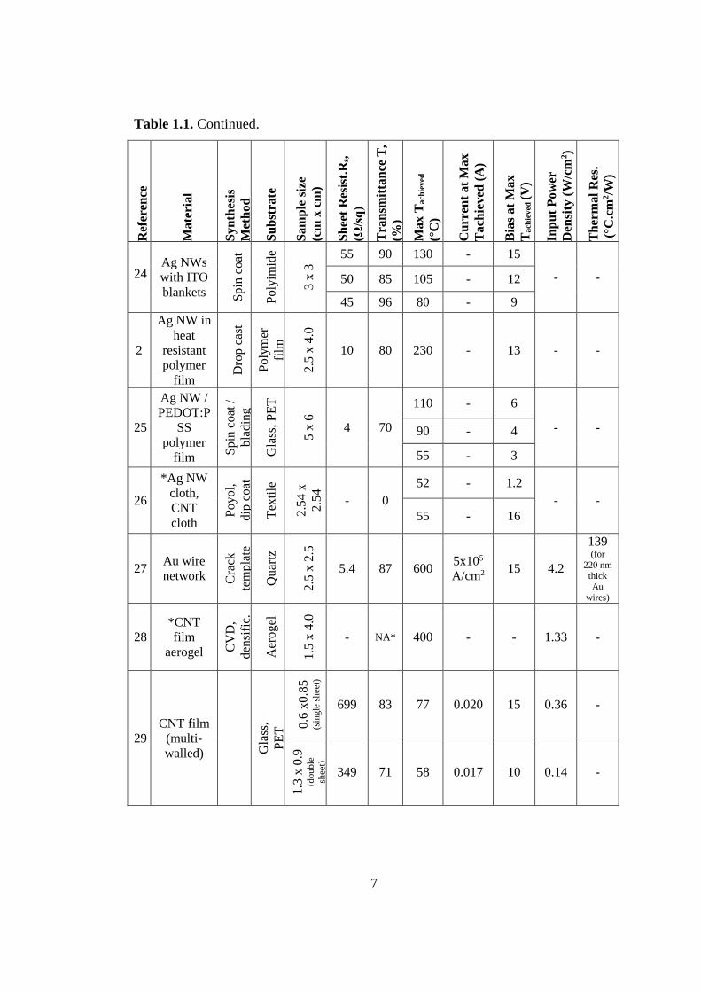
An extensive literature review has been conducted on TTFHs and various properties
of TCMs are tabulated in Table 1.1. Properties such as sheet resistance,
transmittance, maximum temperature achieved under bias, voltage and current
values at the maximum achieved temperature, and thermal resistivity values are
compared within the table. This comparison serves as a general guideline to
demonstrate where networks of Ag NW TTFHs stand in the current scientific
research. A detailed analysis of each TCM (metal oxides, carbon nanotubes,
graphene, metallic nanowires and hybrids of these materials) and their respective
instrinsic properties are discussed in the following sections.
Figure 1.3. a) A silver nanowire based touch-screen panel (Cambrios
ClearOhm)15, b) Structure of a touch-screen panel.16

6
Table 1.1. TTFH properties for various TCMs.
Ref
eren
ce
Ma
teri
al
Sy
nth
esis
Met
ho
d
Su
bst
rate
Sa
mp
le s
ize
(cm
x c
m)
Sh
eet
Res
ist.
Rs,
(Ω/s
q)
Tra
nsm
itta
nce
T,
(%)
Ma
x T
ach
ieved
(°C
)
Cu
rren
t at
Ma
x
Ta
chie
ved
(A
)
Bia
s at
Ma
x
Tach
ieved
(V
)
Inp
ut
Po
wer
Den
sity
(W
/cm
2)
Th
erm
al
Res
.
(°C
.cm
2/W
)
Th
is S
tud
y
Ag NW
Po
lyol,
spra
y
coat
.
Gla
ss,
Quar
tz
2.5
x 2
.5 30 89 175 0.26 11 0.95 -
25 88 180 0.33 9 0.99 -
4.3 83 204 0.74 4 0.99 -
17 Ag wire
mesh
Cra
ck
tem
pl.
Gla
ss
10
x 8
1 77 177 - 9 0.56 255
18
Ag mesh
& ITO
hybrid
PE
T**
3 x
4
300 88 43 0.65 12 0.65 -
4 Ag NW
Soln
,
Spra
y c
oat
.
Gla
ss,
PE
N**
2.5
x 2
.5
35 85 55 - 7 0.24 121
19 Ag NW
with clay
platelets Wet
coat
.
PE
T
5.0
x
7.5
10 90 100 - 7 - -
20 Ag wire,
crackle
precursor
Vac
.evap
.,
spra
y c
oat
.
PE
T,
Gla
ss t
ube
4 x
3
4 x
2 6 86 97 - 5 0.12 515
2 70 92 - 2.25 0.17 409
21 Ag NW
Vac
uum
filt
rati
ng
PE
T,
Quar
tz
2.5
x 2
.5
11 92 138 - 7 - -
22
Ag NW
with
RGO**
sheets
So
lvo-
ther
mal
Qu
artz
2.5
x 2
.5
27 80 225 - 15 - -
23 Ag NW &
CNT**
hybrid
Sp
ray
co
at.,
roll
-to-r
oll
PE
T
4 x
4
- -
110 - 15 - -
70 - 10 - -
40 - 5 0.017 -
7
Table 1.1. Continued.
Ref
eren
ce
Ma
teri
al
Sy
nth
esis
Met
ho
d
Su
bst
rate
Sa
mp
le s
ize
(cm
x c
m)
Sh
eet
Res
ist.
Rs,
(Ω/s
q)
Tra
nsm
itta
nce
T,
(%)
Ma
x T
ach
ieved
(°C
)
Cu
rren
t at
Ma
x
Ta
chie
ved
(A
)
Bia
s at
Ma
x
Tach
ieved
(V
)
Inp
ut
Po
wer
Den
sity
(W
/cm
2)
Th
erm
al
Res
.
(°C
.cm
2/W
)
24 Ag NWs
with ITO
blankets Sp
in c
oat
Po
lyim
ide
3 x
3
55 90 130 - 15
- - 50 85 105 - 12
45 96 80 - 9
2
Ag NW in
heat
resistant
polymer
film
Dro
p c
ast
Po
lym
er
film
2.5
x 4
.0
10 80 230 - 13 - -
25
Ag NW /
PEDOT:P
SS
polymer
film
Spin
coat
/
bla
din
g
Gla
ss,
PE
T
5 x
6
4 70
110 - 6
- - 90 - 4
55 - 3
26
*Ag NW
cloth,
CNT
cloth
Poyol,
dip
coat
Tex
tile
2.5
4 x
2.5
4
- 0
52 - 1.2
- -
55 - 16
27 Au wire
network Cra
ck
tem
pla
te
Quar
tz
2.5
x 2
.5
5.4 87 600 5x10⁵
A/cm2 15 4.2
139 (for
220 nm
thick Au
wires)
28
*CNT
film
aerogel CV
D,
den
sifi
c.
Aer
ogel
1.5
x 4
.0
- NA* 400 - - 1.33 -
29
CNT film
(multi-
walled)
Gla
ss,
PE
T 0.6
x0
.85
(sin
gle
sh
eet)
699 83 77 0.020 15 0.36 -
1.3
x 0
.9
(dou
ble
shee
t)
349 71 58 0.017 10 0.14 -

8
Table 1.1. Continued.
Ref
eren
ce
Ma
teri
al
Sy
nth
esis
Met
ho
d
Su
bst
rate
Sa
mp
le s
ize
(cm
x c
m)
Sh
eet
Res
ist.
Rs,
(Ω/s
q)
Tra
nsm
itta
nce
T,
(%)
Ma
x T
ach
ieved
(°C
)
Cu
rren
t at
Ma
x
Ta
chie
ved
(A
)
Bia
s at
Ma
x
Tach
ieved
(V
)
Inp
ut
Po
wer
Den
sity
(W
/cm
2)
Th
erm
al
Res
.
(°C
.cm
2/W
)
30
CNT film
(multi-
walled) e-b
eam
Gla
ss
5-
layer 172 48 140 - 40 - -
3-
layer 342 67 116 - 40 - -
1-
layer 756 87 100 - 40 - -
31
CNT film
(single-
walled)
Dip
co
atin
g
Gla
ss
2 x
1
22.6
KΩ 96 48 - 60 0.24 90
35.8
KΩ 98 41 - 60 0.15 105
54.6
KΩ 98 38 - 60 0.09 137
32
33
CNT film
(single-
walled) Spra
y
coat
ing
Gla
ss
2.5
x 2
.5
1190 91 210 - 12 0.12 -
34
*CNT film
(double-
walled) CV
D
Gla
ss
6 x
5
- NA* 82 1.5 12 2.06 -
35
CNT film
(single-
walled)
Arc
dis
ch.,
vac
. fi
ltr.
Gla
ss
PE
T
4 x
4
356 76 95 - 12 - -
36 Graphene
CV
D
Gla
ss
2 x
2
66 90 110 - 12 0.14 -
37 Graphene
CV
D
PE
T
4 x
4
43 89 100 - 12 0.20 -

9
Table 1.1. Continued
Ref
eren
ce
Ma
teri
al
Sy
nth
esis
Met
ho
d
Su
bst
rate
Sa
mp
le s
ize
(cm
x c
m)
Sh
eet
Res
ist.
Rs,
(Ω/s
q)
Tra
nsm
itta
nce
T,
(%)
Ma
x T
ach
ieved
(°C
)
Cu
rren
t at
Ma
x
Ta
chie
ved
(A
)
Bia
s at
Ma
x
Tach
ieved
(V
)
Inp
ut
Po
wer
Den
sity
(W
/cm
2)
Th
erm
al
Res
.
(°C
.cm
2/W
)
38 Graphene
CV
D
Gla
ss,
po
lym
er
1 x
1
750 85 80 - 40 - -
39 Graphene
oxide
So
ln.
coat
.
Fle
xib
le
gla
ss
10
x 2
0
5370 45 - - - - -
40 ITO
nanoparticles
So
luti
on
pro
cess
ed,
spin
coat
ed
Gla
ss
-
633 ≥90 163 - 20 2W
- 763 ≥90 100 - 15
3636 ≥90 70 - 10
41 *ITO
nanoparticle
paste film
Spin
coat
.
Quar
tz
1 x
1
23.5 NA* 445 - 12 - -
42
ZnO (Ga
doped) thin
films
Puls
ed l
aser
dep
.
Gla
ss
1.2
5 x
1.2
5
2.14
×10−4
Ω.cm
~90
88 - 12
- - 120 - 15
160 - 20
43
ZnO (Ga
doped) thin
films
RF
mag
net
ron
Gla
ss
1.2
5 x
1.2
5
90 - 42 - - 90 -
44
Ag NW –
copolymer
composite
film Dro
p c
ast.
Sel
f st
and
ing
4 x
1
25 ~80 230 - 13 - -
* Fabricated heaters in these studies are not transparent.
** RGO stands for reduced graphene, CNT stands for carbon nanotube, PET stands
for polyethylene terephthalate, PEN stands for polyethylene naphtalate.

10
It is seen from Table 1.1 that Ag NWs display a high potential to be used as an
alternative material to ITO in TTFHs. Ag NW based TTFHs fabricated in this study
can reach temperatures higher than 175 °C with transmittances higher than 83 %
under applied potentials lower than 12 V. These results compare well with other
TTFH materials. There are only few studies that show similar or better thermal
performances having comparable transmittances under similar applied voltages. One
of these studies involves gold (Au) wire network TTFHs that can reach temperatures
up to 600 °C with transmittances 87 % under an applied potential of 15 V.27 This
result has not been confirmed by another group. Another study involves single-
walled carbon nanotubes that can reach temperatures up to 210 °C with
transmittances 91 % under an applied potential of 12 V.32,33 Another study involves
Ag NW-copolymer composite TTFH that can reach temperatures up to 230 °C with
a transmittance between 78.5 to 81% and a sheet resistance of 25 Ω/sq under an
applied potential of 13 V.
1.2.1. Metal Oxides
Some metal oxides belong to the family of transparent conducting oxide (TCO)
materials with large band gaps (optical transparency requires band gaps larger than
3.3 eV)12 in most cases.
TCOs are n-type semiconductors in which defects such as oxygen vacancies,
impurity substitutions and interstitial atoms in the lattice donate their electrons to the
conduction band providing charge carriers for the transport of electric current.45,46
Therefore, conductivity in n-type TCOs (and generally in other n-type
semiconductors) is a consequence of electron transport.
11
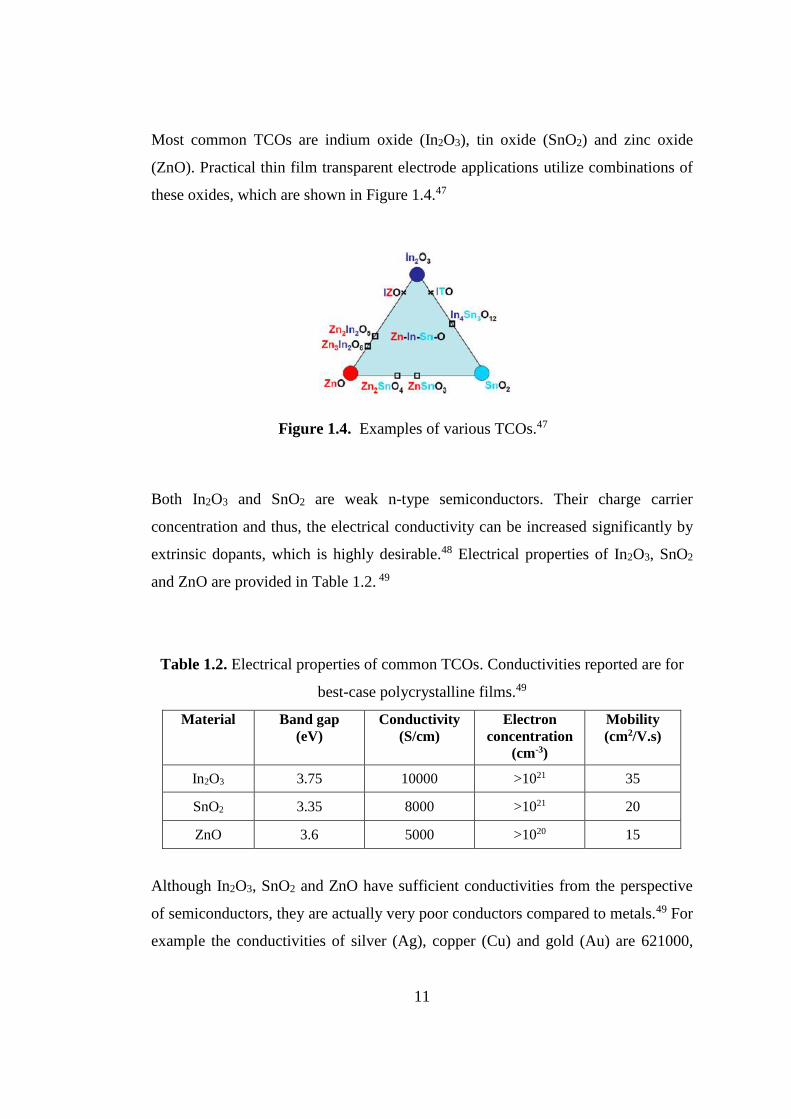
Most common TCOs are indium oxide (In2O3), tin oxide (SnO2) and zinc oxide
(ZnO). Practical thin film transparent electrode applications utilize combinations of
these oxides, which are shown in Figure 1.4.47
Both In2O3 and SnO2 are weak n-type semiconductors. Their charge carrier
concentration and thus, the electrical conductivity can be increased significantly by
extrinsic dopants, which is highly desirable.48 Electrical properties of In2O3, SnO2
and ZnO are provided in Table 1.2. 49
Table 1.2. Electrical properties of common TCOs. Conductivities reported are for
best-case polycrystalline films.49
Material
Band gap
(eV)
Conductivity
(S/cm)
Electron
concentration
(cm-3)
Mobility
(cm2/V.s)
In2O3 3.75 10000 >1021 35
SnO2 3.35 8000 >1021 20
ZnO 3.6 5000 >1020 15
Although In2O3, SnO2 and ZnO have sufficient conductivities from the perspective
of semiconductors, they are actually very poor conductors compared to metals.49 For
example the conductivities of silver (Ag), copper (Cu) and gold (Au) are 621000,
Figure 1.4. Examples of various TCOs.47

12
585000 and 442000 S/cm respectively.50 Therefore, we can conclude that even the
highest TCO conductivity is about a factor of 60 lower than that of the best
conducting metal, Ag. This is one of the reasons why thin films of Ag NWs can be a
good alternative to TCOs in TTFH and other transparent electronics applications.
The theoretical absolute limit of the conductivity for a TCO has been estimated to be
25000 S/cm.51
There are also p-type TCOs. First one to be explored was CuAlO2.49,52 Some of the
other p-type TCO materials include nickel(II) oxide (NiO), potassium doped
strontium copper oxide (SrCu2O2:K), indium(III) oxide-silver(I) oxide (In2O3-
Ag2O), calcium doped copper indium oxide (CuInO2:Ca), copper scandium oxide
(CuScO2:O) and magnesium doped copper scandium oxide (CuScO2:Mg).49
P-type TCOs have very low conductivities with respect to n-type counterparts and
they generally have low optical transmittance. To a large extent, the poor
conductivity of p-type TCOs is due to the very low mobility of these materials,
typically less than ~1 cm2/V.s, compared to mobilities of n-type TCOs (~10-40
cm2/V.s, as shown in Table 1.2).49
1.2.1.1. Indium Tin Oxide (ITO)
Doped metal oxides, in particular ITO, or tin doped indium(III) oxide (In2O3:Sn), is
the conventional and the most important TCM for almost four decades. The first
study on ITO as a transparent conductive oxide was done in 1954.53 ITO on glass is
used as a transparent electrode in nearly all flat panel displays, and this application
represents the largest economic value in TCM thin film coatings industry. The other
major application of TCO is the low-emissivity (low-e) coatings for energy efficient
windows.12

13
Rather than being Sn-doped In2O3, ITO is really an In2O3 rich compound of In2O3
and SnO2 as shown in Figure 1.4. In2O3 is a semiconductor with a band gap of 2.9
eV, while SnO2 is a semiconductor with a band gap of 3.62 eV at 298 K. Sputtered
ITO, has a typical band gap of 3.8 eV.48,54 Sputtered ITO has been reported to
possess a carrier concentration in the range of 14.6-18.9 x 1020 cm-3, mobility in the
range 25.7-32.7 cm2/V.s, resistivity of about 1.3 x 10⁻⁴ Ω.cm, and transmittance of
≥80% in the visible region of spectrum.54
Since ITO demostrates the advantage of such a high optical transmittance between
80-95% in the visible portion of the spectrum and a high electrical conductivity, it
can provide low sheet resistances between 10-1000 Ω/sq.55
However, ITO has some intrinsic disadvantages such as a slow thermal response, it
degenerates into oxygen deficient species when heated above 400 °C, it requires
high vacuum and high temperatures for the deposition, it is not flexible enough and
cracks under mechanical bending, it is unstable in acidic and basic
environments.56,57,58 Moreover, In is a high cost and a scarce material that makes
exploration for ITO alternatives economically feasible.48
There are some patents for use of ITO as a TTFH, specifically in the transparent
toaster application.59,60 It was claimed that ITO (or fluorine doped tin oxide (FTO))
thin film based transparent toasters can reach up to 400 °C temperatures with a high
input power of 1100 W.
Solution-processed ITO nanoparticle based TTFHs are investigated as an alternative
to conventional ITO TTFHs. Thermal responses of these ITO nanoparticle based
TTFHs with respect to the applied voltage are provided in Figure 1.5. It is seen that
these TTFHs may not be ideal for heating applications as they achieve a temperature
of only about 80 °C under an applied potential of 12 V. This temperature might not
be enough for many applications that require higher performance under a maximum

14
applied potential of 12 V.4 12 V is the maximum targeted bias that is applicable in
most defogging and de-icing applications, which is desired to result in temperatures
in excess of 100 °C.
In another study by Yang et al.41, ITO nanoparticle paste and organic additives are
used to fabricate microheaters that can reach a maximum temperature of 400 °C at a
bias of 12 V. Thermal response characteristics of these heaters are provided in
Figure 1.6. However, these heaters were designed for microsensors and no
transparency data was reported.
Because of the previously mentioned disadvantages of ITO, there is extensive
research to develop ITO substitutes. There are some other metal oxide alternatives
such as FTO, ZnO, along with other alternative materials such as carbon nanotubes,
graphene, silver nanowires and hybrid materials. These ITO alternatives are
discussed in the following sections.
Figure 1.5. Thermal response of solution-processed ITO nanoparticles based
TTFHs at various bias conditions.40

15
1.2.1.2. Fluorine Doped Tin Oxide (FTO)
FTO is the dominant material for SnO2-based binary TCOs and the second widely
used TCO. It has better thermal stability for TCE applications with respect to ITO 61,
it is cheaper, highly stable in hydrogen containing environments and it demonstrates
better chemical stability. It is extensively used in dye-sensitized solar cells.48
However, due to its average transparency (~80%), relatively low electrical
conductivity 62 and difficulties in fabrication it is not an ideal alternative to ITO in
TTFH fabrication.48
1.2.1.3. Zinc Oxide (ZnO)
Impurity doped ZnO (e.g., Ga- and Al- doped ZnO (GZO and AZO)) is nontoxic,
abundant in earth’s crust and economically viable that makes it a promising TCO
material, alternative to ITO.63,43 AZO is the best candidate among impurity doped
ZnOs from both the resources and the environmental points of view.47 Both AZO
and GZO have been shown to have low resistivity at high transparencies that gives
Figure 1.6. Thermal response characteristics of ITO nanoparticle paste based
microheaters at various bias conditions.41

16
better performances than ITO in some cases.48 Resistivity of AZO and GZO are
reported as ∼8.5×10⁻⁵ Ω/cm 64 and ∼8.1×10⁻⁵ Ω/cm 65, respectively. These values
are similar to the lowest reported resistivity of ITO that is ∼7.7×10⁻⁵ Ω/cm.66
Resistivity of AZO and GZO also have better thermal stability than that of ITO.48
Another advantage of AZO and GZO is their high optical transparency, which has
typical values of 90% and above,42 comparable to that of ITO. Their high
transparency stems from the wide band gap of the ZnO.48
AZO and GZO also demonstrate better chemical stability at higher temperatures.67,68
The disadvantage of AZO and GZO is that their mass production costs are high.
New methods must be developed to mass produce these films over large areas at
high growth rates with reliable properties.48
1.2.2. Carbon Nanotubes (CNTs)
Carbon nanotubes are one-dimensional materials that are made up of carbon atoms
in the form of rolled-up graphene. They can be single-walled (SWCNT) or multi-
walled (MWCNT). After their discovery in 1991,69 there have been extensive
studies that demostrate CNT’s peculiar properties, which include high electrical
conductivity of 106 S/m2 (for SWCNTs)35 and high thermal conductivity of 3500
W/m.K.31 However, as far as transparent conductve film applications are concerned,
CNTs can not achieve the minimum standards set by industry (T ≥ 90% and Rs <
100 Ω/sq, see ref [22] of Scardaci et al. 201111). A few examples on reported
transparencies together with respective sheet resistances are 90% and 756 Ω/sq for
MWCNTs 30, 79% and 580 Ω/sq for SWCNTs 32, 70% and 130-190 for SWCNTs 33,
85% and 1000 Ω/sq for SWCNT 70. The reason that higher transparencies result in

17
high sheet resistances in CNTs is the intertube contact resistances 71 and presence of
semiconducting SWCNTs.
Figure 1.7. shows TTFH performance of CNT thin films with 3 different sheet
resistances. It is clear that these TTFHs need higher voltages than 12 V to reach
targeted 100 °C.30
1.2.3. Graphene
Graphene is a monolayer solely made up of carbon atoms that form a two
dimensional hexagonal lattice with each atom at the vertex.72
There are two seminal works on TTFH application of graphene. In terms of TTFH
performance at an applied bias of 12 V, Bae et al. reported a Tmax of 110 °C (66
Figure 1.7. Heating performance of MWCNT sheet heaters.30

18
Ω/sq and 90% transparency) 36 and Kang et al. reported a Tmax of 110 °C (43 Ω/sq
and 89% transparency) 37. These studies both satisfy industrial requirements for
TCEs, T ≥ 90% and Rs < 100 Ω/sq as set by Hewlett-Packard (see ref [22] of
Scardaci et al. 201111). However, they fail to show competitive heating
performance.
1.2.4. Metallic Nanowires
Metallic nanowires have at least two dimensions between 1 and 100 nm. Due to
their dimensions and confinement effects they have interesting optical, magnetic,
electrical and thermal properties. 73
The most promising nanostructured material is probably Ag NWs 11 as they can be
simply grown in solution and deposited from solution, are stable under flexing and
networks of Ag NWs have low sheet resistances (Rs < 100 Ω/sq) at high
transparencies (T ≈ 85%). Due to their low optical conductivity, Ag NW networks
display high optical transmittance for a given thickness.74
In optical conduction, some of the photons passing through the material annihilate
and lose their energy to excite the electrons within the material to the conduction
band. So these electrons move across the material, forming an electrical current.
Therefore low optical conductivity of a TCM is desired, because as lesser photons
are annihilated higher optical transmittance is achieved.
Apart from Ag, the two most common metallic nanowires are Au and Cu. TTFH
studies on Cu NWs are still in their infancy.

19
1.2.4.1. Silver Nanowires (Ag NWs)
Among metals, Ag has the highest thermal conductivity and the lowest electrical
resistance, thus it is predominant candidate for the fabrication of TTFHs.4
Additionally, it is estimated that Ag NW thin films have a material cost of ~30 $/m2
11 comparable to the cost of commercial ITO-coated glass 75. Ag NW synthesis is
also easy, while large-scale synthesis of other metallic nanowires have not been
reported so far.76 Inherited from the intrinsic propertes of Ag, networks of Ag NWs
have advantages of high flexibility, high optical transmittance and high heating
performance under low applied bias (generally below 12 V) that is of interest for
many applications.4
In comparison to CNT thin films, thermal annealing of thin films of metallic
nanowires cause a significant reduction in electrical resistance due to desorption of
organic residues and sintering at the local junctions between the nanowires under
constant optical transmittance. This is a major advantage of metallic nanowires
against CNTs, which have high junction resistance between nanotubes as discussed
earlier.77
Moreover, Ag NW thin films display much higher figure of merits (direct current to
optical conductivity ratio) than Ag thin films with similar thicknesses.78
1.2.4.2. Gold Nanowires (Au NWs)
Au NWs are another type of metallic nanowires that may have a high potential for
their use as TTFHs, since extraordinary optoelectronic properties have been reported
solely by a group. A sheet resistance of 5.4 Ω/sq has been reported at 87%
transmittance (at 550 nm wavelength), with a maximum thermal response of 600
°C.27 However, these results are not confirmed or reproduced by another group.

20
1.2.5. Hybrid Materials
There are a number of studies that involve hybrid TCMs, few of which are provided
with their properties in Table 1.3. Nanowire junctions increase the overall sheet
resistance of the thin films. The driving force for the fabrication of hybrid materials
is to decrease this junction resistance by the second material. Although not reported,
these hybrid materials may have potential to be used as TTFHs.
Table 1.3. Hybrid transparent conducting materials.
Ref. Hybrid TCM Sheet Resistance
(Ω/sq.)
% Transmittance
(550 nm)
79 Ag NW – Au NP – RGO 86 85
80 Ag NW mesh – Graphene 14 90
81 Ag NW – ITO 12 85
82 Ag NW – SnO 28 82
83 CNT – ITO 55 90
84 Cu NW – Ni NW 60 84
1.3. Silver Nanowire Thin Films
1.3.1. Percolation Theory and Optoelectronic Properties of Nanowires
Conduction in Ag NW networks can be described by “Percolation Theory” as
explained schmetically in Figure 1.8. Ag NWs tend to coalesce together more and
more, and finally they reach a point called as “percolation threshold” (Pc) in which
most of the NWs have formed intersections that can carry current through the
network. Once NW density extends the percolation threshold, low sheet resistance
can be obtained; however, this considerably reduces the transmittance.85 Therefore,
optimum conditions must be found without sacrificing either sheet resistance or

21
optical transmittance.86 Another parameter that can affect Pc is the NW length.
Using longer NWs shifts percolation threshold curve to left in Figure 1.8, meaning
that samples with longer NWs display higher conductivity at lower percentage of
NW projection area to the sample area.
In order to compare optoelectronic properties of different TCMs, one can define
“Figure of Merit” (FoM), which is based on the considered physical properties. FoM
is defined as 87:
FoM = T10 / Rs
, where T is transparency at 550 nm, and Rs is sheet resistance of the film.76
When FoMs of different TCMs are compared, as shown in the plot given in Figure
1.9., it is seen that the material whose FoM is closest to that of ITO is thin films of
Ag NWs. 76
Figure 1.8. Percolation theory explained through conductivity as a function of
percentage of NW projection area to the sample area.

22
1.3.2. Joule Heating Mechanism of Nanowire Networks
TTFHs convert electrical energy into heat by the so-called “Joule Heating
Mechanism”. Joule heating is the characteristic of a material that allows heating of a
material when there is a current flow. As electrons flow through the material,
electrical energy is transformed into thermal energy due to the partial loss of moving
electrons’ energy to the vibration of the lattice phonons (vibrational modes of ions
that make up the lattice).88,89 As the vibrational energy of lattice ions increases,
temperature of the conducting body increases, allowing the TTFH to work as
intended.
Power (P) converted from electrical energy to thermal energy can then be calculated
by the following equation:
P = I . V = I2 . R = V2
R
Figure 1.9. Transparency versus sheet resistance for various TCMs.76

23
, where I is the current through the resistor, R, and V is the voltage drop across the
resistance.88 This equation is valid for direct current (DC).
Example in Table 1.4 is provided to demonstrate how the dissipated power changes
under a fixed applied bias across two points with varying resistances. As shown in
the table, higher heat dissipation can be obtained at lower resistances for a fixed
bias. This implies that utilizing thin films of metallic nanowires as TTFHs is
advantageous since they have very low sheet resistances under high optical
transmittance. Therefore, they can dissipate more power at a low applied bias.4
Table 1.4. Dissipated power change under a fixed applied bias across two points
with varying resistances.
1st case
2nd case
3rd case
Applied bias
(fixed) V V V
Resistance R 2 R 5 R
Current 10 I 5 I 2 I
Power dissipated 100 I2R 50 I2R 20 I2R
The maximum steady-state temperature achieved in a TTFH is set by a balance
between Joule heating and heat dissipation, which can be controlled by the applied
bias.13 Increasing bias voltage decreases the mean free time of the electrons that
result in an intensified scattering rate and more resistive losses due to optical
phonon emission mechanism.90
24
1.3.3. Failure Mechanism of Nanowire Networks due to Joule Heating
Current through a thin film of metallic nanowires travels within the nanowires,
rather than uniformly distributed throughout the whole film. This great reduction in
current flow area causes major increase in the current density, which in turn
increases temperature sharply due to Joule heating. Therefore, Joule heating causes
melting in the nanowire structure, which hinders performance of TTFHs. The
network with higher sheet resistance will carry higher current density and it will fail
more easily due to Joule heating. 91
Moreover, metallic nanowires are known to have an energetic instability called
“Rayleigh instability”. This is an important issue for the long-term reliability of the
devices.77 Rayleigh instability occurs due to the diffusion of surface atoms in a
metallic NW. Surface diffusion results in the fragmentation of a NW into spherical
fragments at temperatures much lower than the melting point of the parent metal and
the metallic NW.92
In addition, Joule heating also plays a role in a process called “electromigration” in
which atoms in a device are displaced due to momentum transfer between charge
carriers and the lattice 93. Electromigration is related to the transport of mass in
metals when the metals are stressed at high current densities 94.
1.4. Ag NW Synthesis by the Polyol Method
Controlling size of the nanowires through synthesis is very crucial as the intrinsic
electrical and optical properties of nanostructures are determined by their
dimensions.73 Since bulk Ag has a high thermal conductivity and the highest
electrical conductivity among other metals, synthesis of Ag NWs is an active

25
research area, especially since 2013. Therefore, many synthesis methods have been
developed to synthesize Ag NWs.
Ag NW synthesis methods include chemical synthesis,95,96 electrochemical
technique,97,98 hydrothermal method,99,100 UV irradiation photodetection
technique,101,102 DNA template,103,104 porous materials template,105,106 and polyol
process.107,108 (references are taken from Coskun et al.109). Vapor phase synthesis
methods are mainly physical deposition methods, such as electron-beam deposition.
On the other hand, because of the advantages of the nature of homogeneous
reactions, wide range of solutions, simple monitoring technology and low cost,
liquid phase synthesis methods are generally preffered.73 Especially for the
development of transparent flexible electrodes, synthesis of the required electrode
materials using low-cost solution-based processes is one of the most important
arguments.76
When compared to other synthesis methods, the polyol approach appears as the
most promising solution-based synthesis method due to its ease of mass production,
cost and simplicity.76 Polyol method involves production of the targeted metalic
nanoparticles in colloidal form through reduction of inorganic salts by a polyol at
mediocre temperatures.
Polyol synthesis was introduced by Fievet and co-workers for the synthesis of
colloidal metallic nanoparticles such as Ag, Au, Cu, cobalt (Co), palladium (Pd),
iridium (Ir), platinum (Pt), ruthenium (Ru), cobalt-nickel alloy (CoNi), and iron-
nickel alloy (FeNi).110,111,112,113,114
Xia et al. were first to successfully synthesize size- and shape-controlled single-
crystal Ag nanoparticles along with other nanostructures using polyol process.115
After their work, metal nanostructures are widely synthesized by many research
groups.73 In this method, typically ethylene glycol (EG) is used as both the solvent

26
and the reducing agent, poly(vinylpyrrolidone) (PVP) is used as the stabilizing
polymer (stabilizing agent), and silver nitrate (AgNO3) is used as the Ag source.
In a slightly modified version of polyol process, a trace amount of a salt, such as
sodium chloride (NaCl), iron(III) nitrate (Fe(NO3)3), copper(II) chloride (CuCl2) or
copper(I) chloride (CuCl) is added to the solution in order to control the morphology
of the final products. This modified method is called as “salt-mediated polyol
method”. Salt-mediated synthesis strategy is a simple and effective method, which is
useful for the mass synthesis of Ag NWs. 73
In the polyol synthesis of Ag NWs 109, EG solution of PVP is prepared. NaCl is
added to this solution. Solution is heated to elevated temperatures (optimum
temperature is found to be 170 °C). AgNO3 is added dropwise to EG+PVP+NaCl
solution under continuous stirring. With the introduction of Ag+ ions into the
solution, Ag nanoparticles start to form via homogeneous nucleation. Chemical
adsorption of PVP molecules onto the surfaces of as-formed Ag nanoparticles is the
reason for them to remain at nanoscale.116 As the process continues, some of the Ag
nanoparticles start to dissolve and grow as larger nanoparticles via the mechanism
known as Oswald ripening.117 With the passivation of some facets of these particles
by PVP (stabilizing agent), some nanoparticles can grow into multitwin particles.
PVP is believed to passivate (100) faces of these multitwin particles and leave (111)
planes active for anisotropic growth at [110] direction. As the addition of Ag+ ions
continue, multitwin particles grow into Ag NWs. Final color of the growth solution
indicates the formation of NWs. Following synthesis, centrifuging is carried out to
purify the NWs by separating polymer and metallic by-products (nanoparticles etc.).
A schematic governing the synthesis mechanism of Ag NWs via solution based
polyol process is provided in Figure 1.10. 109

27
Coskun et al.109 found out that the temperature, AgNO3 injection rate, PVP/AgNO3
(stabilizing agent/reducing agent) ratio, amount of NaCl added to the solution and
stirring rate have important effects on the formation and dimensions of Ag NWs.
Following conclusions are drawn:
• Optimum polyol synthesis process temperature is 170 °C. Below a certain
temperature, high aspect ratio Ag NW formation is not possible. The length
distribution of NWs widens beyond 170 °C.
• AgNO3 injection rate affects the final morphology of Ag nanostructures.
• Deficient and excess amounts of PVP over AgNO3 result in the formation of
undesired Ag structures in addition to nanowires.
• Absence of NaCl results in the formation of only Ag particles. the amount of NaCl
that needs to be added to growth solution is 12 μM. Beyond this optimum value,
due to oversaturation, micrometersized Ag particles start to grow dominantly,
suppressing Ag NW formation.
• Stirring rate affects the diameter and length of Ag NWs. As stirring is done faster,
the diameter and length of the Ag NWs decrease.
Figure 1.10. A schematic of the synthesis mechanism of Ag NWs via solution
based polyol process. 109

28
As detailed in the Experimental section, optimum values of these parameters were
used to synthesize Ag NWs for the fabrication of TTFHs in this thesis.
1.5. Ag NW Transparent Thin Film Heater Fabrication by Spray Coating
Achieving high reproducibility in deposition of colloidal solutions as thin films is
often difficult.76 Drop casting thin films of NWs exhibit inhomogeneities known as
‘coffee ring effect’ on the substrates during the solvent evaporation step.118,119 Films
obtained through air-sprayed coatings are usually more homogeneous and tend to
form much more uniform networks. In addition to this advantage, spray coating is
also regarded as a fabrication method that is cheap, easy, conducted at low
temperatures, compatible with various substrates and very suitable for scale-up.11 It
is also highly amenable to produce patterned films.12
Spray coating of Ag NWs onto substrates in order to form network Ag NW TTFHs
involves pressure controlled spraying of nanowire suspensions by a spray gun onto
the target substrate. Substrate is kept at an elevated temperature for instant removal
of solvent through evaporation. Spray coated Ag NW thin films based transparent
conducting films have been successfully achieved in many studies.120,121,4,11 Spray
coating has also been used to deposit SWNT networks.122,123 In the case of heat sink
applications, spray-coated Ag NWs on glass substrate are found to be well coupled
to each other, thereby forming a continuous heat transfer pathway.124 In the case of
solar cell applications, depending on the experimental conditions used for their
fabrication, thin films of metallic nanowires can have haze factors varying between
1 and 30%.125 If low haze factor is desired, this can be achieved utilizing spray
deposition, which can lead to haze factors below 2%. Such haziness is acceptable
for display and window applications. 76

29
Different deposition routes for alternative TCMs are compared in Table 1.5.76 As
given in the table, spray coating (or spray deposition) is the best method for the
fabrication of transparent conducting electrodes using Ag NWs.
Table 1.5. General guide to transparent conducting electrode fabrication.76
Fabrication
Method* Ag NWs TCOs Graphene CNTs
CVD - +++ +++ +
Sputtering - +++ - -
Spin coating ++ - + ++
Spray deposition +++ ++ + +++
Screen printing ++ - + ++
Cost Medium Low - High High High
* Fabrication method refers to the production of electrodes directly, not to the
production of the constituent components which are used to fabricate the network.

30

31
CHAPTER 2
EXPERIMENTAL
2.1. Networks of Ag NWs for the Fabrication of TTFHs
2.1.1. Ag NWs Synthesis
For the synthesis of Ag NWs and their further purificaton including formation of
NW suspensions, procedures reported by Coskun et al.109 were followed.
All chemicals used in the synthesis procedure were purchased from Sigma Aldrich
and used without further purification.
Prior to the synthesis, all glassware and substrates to be used in the experiments
were cleaned. The cleaning procedure started with rinsing tools with deionized
water. After that glasswares were washed with basic solution with pH 11, acidic
solution with pH 2 and sonicated 10 minutes each within acetone (99.8%) and
isopropyl alcohol (99.8%) baths. Finally, to get rid of chemical residues they were
thourougly rinsed with deionized water (with an electrical conductivity of 18.3 MΩ)
and dried under nitrogen flow.
Following cleaning of the glassware, Ag NWs were synthesized through polyol
process. For polyol process, 10 mL of 0.45M ethylene glycol solution of PVP
(monomer-based calculation MW = 55 000) was prepared and 7 mg of 99.5% pure
NaCl was added into this solution. The solution was heated at 170 °C in a two-
necked round flask. 0.12 M AgNO3 (99.5%) solution in 5 mL of EG was prepared

32
and added dropwise into the PVP solution by an injection pump (Top-5300 model
syringe pump) at a rate of 5 mL/h. PVP:AgNO3 molar ratio was 7.5 : 1. The solution
was stirred at a rate of 1000 rpm by a magnetic stirrer during the whole process.
At the end of the synthesis, in order to separate polymer from the Ag NWs, the
solution was diluted with acetone (in a ratio of 1:5) and centrifuged two times at
6000 rpm for 20 min. After that, NWs were dispersed in ethanol and again
centrifuged at 6000 rpm for 20 min. A photo of ethanolic solution of Ag NWs
following purification is given in Figure 2.1. Final solution color indicated the
presence of Ag NWs. Ethanolic solution was used for the further deposition of Ag
NW thin films via spray coating.
Typical diameter and length of the NWs synthesized in this work were 60 nm and
10 µm on average, respectively. XRD peaks of the synthesized NWs in this study
were shown to belong to pure silver (JCPDS Card No. 04-0783).127
Figure 2.1. Ethanolic solution of Ag NWs following purification.
33
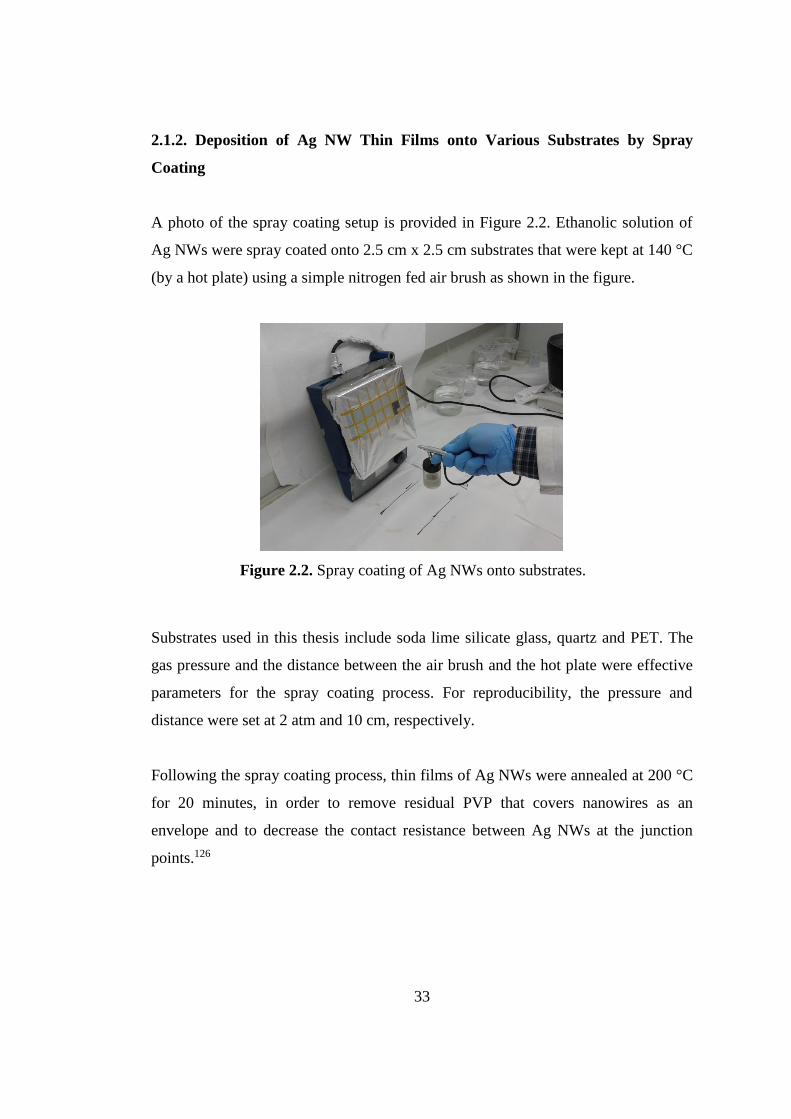
2.1.2. Deposition of Ag NW Thin Films onto Various Substrates by Spray
Coating
A photo of the spray coating setup is provided in Figure 2.2. Ethanolic solution of
Ag NWs were spray coated onto 2.5 cm x 2.5 cm substrates that were kept at 140 °C
(by a hot plate) using a simple nitrogen fed air brush as shown in the figure.
Substrates used in this thesis include soda lime silicate glass, quartz and PET. The
gas pressure and the distance between the air brush and the hot plate were effective
parameters for the spray coating process. For reproducibility, the pressure and
distance were set at 2 atm and 10 cm, respectively.
Following the spray coating process, thin films of Ag NWs were annealed at 200 °C
for 20 minutes, in order to remove residual PVP that covers nanowires as an
envelope and to decrease the contact resistance between Ag NWs at the junction
points.126
Figure 2.2. Spray coating of Ag NWs onto substrates.

34
A photo of the quartz substrate with Ag NW thin film together with its optical
microscope image is shown in Figure 2.3. Barely resolved Ag NWs are evident in
the optical microscope image.
2.1.3. Physical Vapor Deposition of Ag Contacts on Ag NW Networks
Prior to the formation of Ag contacts by thermal evaporation, Ag NW network film
coated substrates were masked using a shadow mask with the desired pattern.
Equipment used in deposition of Ag thin films was Nanovak NVTH-350.
Ag deposition was not started until a base pressure of about 1.0 x 10⁻⁶ Torr was
achieved. Pressure increased during deposition but never exceeded 1.0 x 10⁻⁵ Torr.
Deposition was carried out at a current range of 45-60 A, voltage between 2.0-2.3 V
and deposition rate between 1.5-2.0 Å/s. Deposition was finalized at a Ag thickness
of 200 nm, monitored through a thickness monitor.
Figure 2.3. A photo of (a) Ag NW thin film coated on quartz sample,
(b) optical microscope image of this film.

35
The interface between contact zone and Ag NW thin film is examined by the optical
microscope images provided in Figure 2.4. Figure 2.4 (a) shows that the Ag NWs
were wetted with Ag NW thin films; whereas Figure 2.4 (b) shows that the wetting
was failed. The reason for failure as shown in the figure was the use of aluminum
foil as the shadow mask in this sample. Following this, a proper mask was designed
and got fabricated from a 1 mm thick aluminum plate and used for further
experiments.
Dimensions of the Ag NW thin film deposited substrate and Ag contacts is given in
Figure 2.5, defined by the shadow mask. Apart from this design, two other
geometries were also investigated with no luck, as will be discussed in Chapter 3.
Figure 2.4. Optical images of the interface between Ag NWs and Ag thin films
showing (a) a succesful wetting and (b) a failed wetting.

36
2.1.4. Electrical Wiring and Cable Bonding
Finally, electrical cables made of constantan were bonded to Ag contacts to finalize
the TTFH fabrication. Bonding between endpoints of cables and Ag contacts were
achieved by applying 2-component Ag filled epoxy (Elecolit 320H) followed by
annealing at 100 °C for 1 hour. Final structure of the TTFH devices fabricated in
this work is shown in the photo provided in Figure 2.6.
Figure 2.6. A photo showing the final structure of the fabricated TTFHs in this
work.
Figure 2.5. Dimensions of substrate and Ag contacts utilized in this work.

37
2.2. Infrared Imaging and Thermal Mapping for the TTFH Devices
Infrared (IR) thermal measurements were done on a “QFI MWIR-512 InSb IR FPA
Camera” equipped with “QFI MWIR-SE High Speed Thermal Transient Detector”
with InfraScope TM MWIR Temperature Mapping InSb Focal Plane Array
attachment.
Samples were attached on the camera’s aluminum plate that was held at 85 °C in
order to heat the samples for achieving IR images that has enough contrast to be
differentiated from background radiation. TTFH samples’ below surfaces were
coated with a thermal grease (GC Electronics Type Z9 Heat Sink Compound) in
order to achieve heat conduction between the plate and samples during
measurements.
Electrical potential difference was applied between Ag contacts while IR camera
detected and showed temperature distribution across the whole sample surface. A
schematic on how temperature detection and thermal mapping was made for the
TTFH samples is given in Figure 2.7.
Figure 2.7. Thermal mapping in IR thermal camera setup.

38
Power was supplied through Ag contacts of TTFH samples by an Agilent 6032A
system power supply unit. Either voltage or current was supplied through the unit.
2.3. Thermal Measurements under Bias
In addition to thermal imaging, performance of the TTFH samples under various
applied potentials were investigated using a custom built setup, schematics of which
is provided in Figure 2.8.
Components of the setup include a power supply (Agilent 6032A system power
supply unit, or Agilent N6744B DC power module attached to Agilent N6700B low
profile MPS mainframe), a data acqusition unit (Agilent 34970A data
acqusition/switch unit), a digital multimeter (Agilent 34401A) and a personal
computer.
Figure 2.8. Thermal measurement setup utilized in this work.

39
Temperature measurements were taken via 4 different fine wire thermocouples (J-
type, iron-constantan) linked to the data acqusition unit. Thermocouples were
attached to back surfaces of the TTFH samples by Kapton tape as shown in Figure
2.9.
2.4. Scanning Electron Microscopy Imaging
Ag NW thin films were analyzed by Field Emission Scanning Electron Microscopy
(FE-SEM) (Nova NanoSEM 430) operated at 10 kV voltage.
SEM images have been taken from the Ag NW thin films deposited on silicon
wafers (p-type, single crystalline, 100 oriented). These wafers were placed next to
other samples during spray coating of Ag NW thin films. Thus, the silicon samples
and the TTFHs have identical NW densities. No further gold or carbon coating was
utilized during imaging.
Figure 2.9. A photo showing how the temperature measurements were taken via
thermocouples.

40
2.5. Sheet Resistance Measurements
Sheet resistance measurements were conducted by a two-probe setup which was
able to measure Rs values accurately for the range involved.127 During the
measurements, a known current is sourced and it flows through an unknown
resistance. A problem that occurs when using a 2-wire setup is that the voltage is
measured not only across the resistance in question, but also includes the resistance
of the leads and contacts. These parasitic resistances, however, are not creating a
problem since the sheet resistances of the thin films were around a few ohms.
Sheet resistances of the samples were measured by 2-probe measurements, and a
schematic of the setup is provided in Figure 2.10. 127
2.6. Transparency Measurements
The optical transmittance of Ag NW thin film samples were measured using a UV-
VIS setup (Varian-Cary100 Bio) within the wavelength range of 300-800 nm at
room temperature. In UV-VIS analyses, bare glass was used as the reference
substrate for baseline correction. Although transmittance data is obtained as a
spectra, for the sake of simplicity it is usually reported as a unique percentage value
taken at a wavelength of 550 nm.
Figure 2.10. Two probe setup used for the measurement of sheet resistances of
the thin films.127

41
CHAPTER 3
RESULTS AND DISCUSSION
3.1. Effect of Contact Geometry
3.1.1. IR Thermal Camera Temperature Mappings
TTFHs with Ag NW networks on soda lime silicate glass subtrates with 3 different
contact geometries were fabricated. Temperature distribution of each sample under
bias was monitored by the thermal camera. Obtained images with respect to the
contact geometries are provided in Figure 3.1. (a), (b) and (c).
Device in Figure 3.1 (a) had parallel contact geometry. This sample could withstand
temperatures up to 180 °C. Ag NW thin film was properly functioning when the
sample failed due to cracking of the glass substrate at 180 °C (corresponding to an
applied bias of 9.8 V and a resulting current of 2.3 A). As will be discussed, in
Figure 3.2 no difference in the structure of Ag NW networks were observed
following the application of bias.
Device in Figure 3.1 (b) had a 4-contact geometry. This sample could withstand
temperatures around 120 °C (corresponding to an applied bias of 9.0 V and a
resulting current of 2.0 A). Temperature at the corners were higher than 180 °C at
the time of failure at 120 °C (mean sample temperature). The reason for the failure
is melting of the Ag NWs at the corners due to high current and high temperature at
the sharp edges of contacts as shown in the thermal image at the inset.
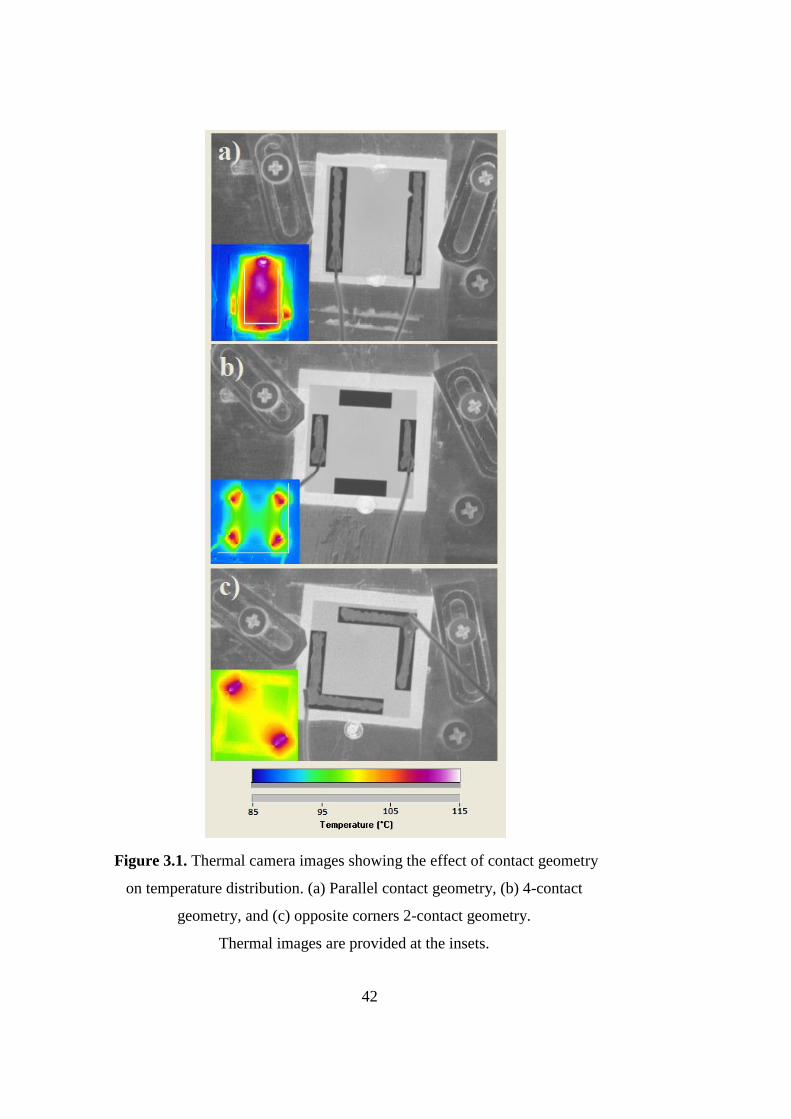
42
Figure 3.1. Thermal camera images showing the effect of contact geometry
on temperature distribution. (a) Parallel contact geometry, (b) 4-contact
geometry, and (c) opposite corners 2-contact geometry.
Thermal images are provided at the insets.
Thermal images are provided at the insets.

43
Device in Figure 3.1 (c) on the other hand, had an “L” shaped 2-contact geometry at
opposite corners. This sample could withstand temperatures around 110 °C
(corresponding to an applied bias of 4.5 V and a resulting current of 2.2 A).
Temperature at the corners were higher than 170 °C at the time of failure at 110 °C
(mean sample temperature). Similar to the device in Figure 3.1 (b), the reason for
the failure is melting of the Ag NWs at the corners due to high current and high
temperature at the sharp edges of contacts as shown in the thermal image at the
inset.
It is concluded that sharp corners having small distances in between, result in high
electrical flux and must be avoided. Therefore, TTFHs having two parallel contacts
on the opposites sides achieve the most homogeneous temperature distribution,
withstand higher temperatures and currents before the failure of Ag NW networks.
It is also predicted that Ag NW networks can withstand temperatures higher than
180 °C provided that the substrate withstands to those temperatures without
cracking.
Figure 3.2. Optical microscope images of Ag NW thin films at the contact
interface in parallel contact geometry (a) before and (b) after
bias voltage application.
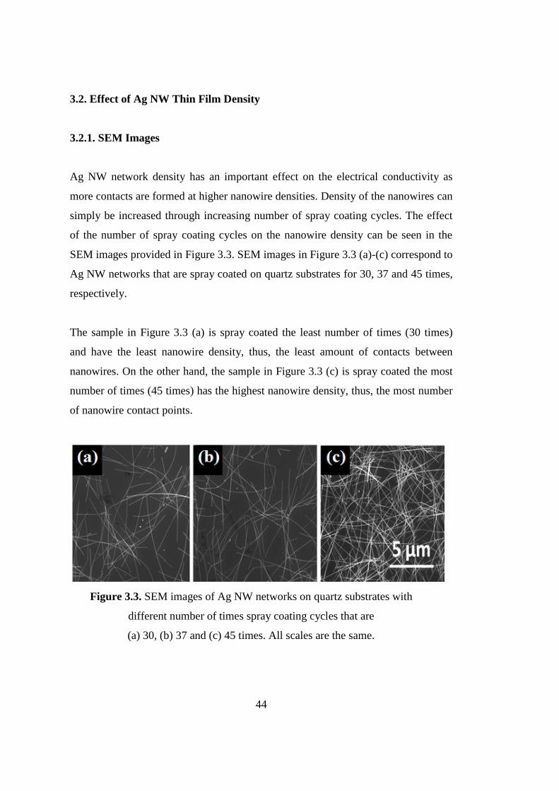
44
3.2. Effect of Ag NW Thin Film Density
3.2.1. SEM Images
Ag NW network density has an important effect on the electrical conductivity as
more contacts are formed at higher nanowire densities. Density of the nanowires can
simply be increased through increasing number of spray coating cycles. The effect
of the number of spray coating cycles on the nanowire density can be seen in the
SEM images provided in Figure 3.3. SEM images in Figure 3.3 (a)-(c) correspond to
Ag NW networks that are spray coated on quartz substrates for 30, 37 and 45 times,
respectively.
The sample in Figure 3.3 (a) is spray coated the least number of times (30 times)
and have the least nanowire density, thus, the least amount of contacts between
nanowires. On the other hand, the sample in Figure 3.3 (c) is spray coated the most
number of times (45 times) has the highest nanowire density, thus, the most number
of nanowire contact points.
Figure 3.3. SEM images of Ag NW networks on quartz substrates with
different number of times spray coating cycles that are
(a) 30, (b) 37 and (c) 45 times. All scales are the same.

45
3.2.2. Transparency, Sheet Resistance and Nanowire Density
The transmittance values at 550 nm corresponding to different sheet resistances of
Ag NW networks that are 30, 37 and 45 times coated on quartz substrates with their
respective calculated NW densities are tabulated and provided in Table 3.1.
Table 3.1. Sheet resistance, transmittance values at 550 nm and respective NW
densities of 30, 37 and 45 times spray coated samples.
Sample (# of times coated)
Sheet Resistance
(Ω/sq)
Transmittance
(550 nm) (%)
NW Density
(NW/µm2)
30 30 89.6 ~ 0.5
37 25 88.3 ~ 0.6
45 4.3 83.6 ~ 1.6
As shown in Table 3.1, NW density values are interpolated according to sheet
resistance values and the respective transmittances obtained in our group. Actual
values are calculated from SEM images using ImageJ software (developed by
Wayne Rasband).
It is concluded from Table 3.1 that as NW density is increased, number of NW
contacts are increased, which in turn increases conductivity and reduces the sheet
resistance. On the other hand, since there are more NWs per unit area in a denser
sample, transparency is decreased due to higher absorption (or higher scattering) of
light passing through the TTFH.
Optical transmittance spectra of samples with densities of 0.5, 0.6 and 1.6 NW/µm2
are given in Figure 3.4.

46
3.2.3. Thermal Measurements Under Bias
Figure 3.5 shows the thermal behaviour of TTFHs with Ag NW thin films on quartz
substrates with respect to time at an applied bias of 4 V for NW densities of 0.5, 0.6
and 1.6 NW/µm2. Heating and cooling rate as a function of time for the sample
having NW density of 1.6 NW/µm2 is also given at the inset.
Attained maximum temperature values at an applied bias of 4 V at the end of 20
minutes of application of bias for 3 different nanowire densities are tabulated and
provided in Table 3.2.
Figure 3.4. Optical transmittance spectra of samples with Ag NW densities
of 0.5, (b) 0.6 and (c) 1.6 NW/µm2.

47
Table 3.2. Maximum temperature reached at 4 V bias for samples with NW
densities of 0.5, 0.6 and 1.6 NW/µm2.
Sample (NW density - NW/µm2)
Rs (Ω/sq) Max. temperature
achieved at 4 V bias
0.5 30 55
0.6 25 62
1.6 4.3 204
Figure 3.5. Change in temperature as a function of time at an applied bias
of 4 V for samples with NW densities of 0.5, 0.6 and 1.6 NW/µm2.
Heating and cooling rate as a function of time for the sample with NW
density of 1.6 NW/µm2 is given at the inset.

48
Table 3.2 clearly shows that TTFHs having higher nanowire densities (therefore
lower sheet resistances) can reach higher maximum temperatures under the same
applied bias. This is in consistency with the comment given for Table 1.4 that higher
heat dissipation can be obtained for networks with lower sheet resistances under a
fixed bias.
3.3. Effect of Bias Voltage
Effect of bias voltage on the temperature behaviour of TTFHs with Ag NW
densities of 0.5, 0.6 and 1.6 NW/µm2 is given in Figure 3.6. Applied voltages and
corresponding current values are marked on the curves. For these measurements,
voltage was applied for 20 minutes and then it was turned off for another 20
minutes.
Achieved maximum temperature (Tmax), in conjunction with the applied bias,
corresponding current and calculated power densities are tabulated and provided in
Table 3.3.
Table 3.3. Thermal response characteristics at maximum achievable temperature of
samples with Ag NW densities of 0.5, 0.6 and 1.6 NW/µm2.
Sample (NW/µm2)
Sheet
Resistance
(Ω/sq)
Tmax
achieved
(°C)
Bias
at Tmax
(V)
Current
at Tmax
(A)
Input Power
Density*
(W/cm2)
0.5 30 175 11 0.26 0.95
0.6 25 180 9 0.33 0.99
1.6 4.3 204** 4 0.74 0.99
* Effective sample area is taken as 3 cm2 (with regard to dimensions of 2.5 cm x 1.2 cm, see Figure 2.5).
** Sample begins to lose stability after reaching a maximum temperature of 204 °C as seen from Figure 3.6.
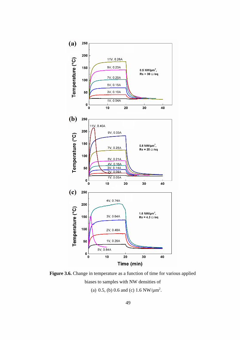
49
Figure 3.6. Change in temperature as a function of time for various applied
biases to samples with NW densities of
(a) 0.5, (b) 0.6 and (c) 1.6 NW/µm2.

50
It is seen from Table 3.3 that the achieved maximum temperature is 204 °C under an
applied potential of 4 V bias for the sample with Ag NW density of 1.6 NW/µm2.
However, this maximum temperature was not stable. The maximum stable
temperature was 180 °C under an applied bias of 9 V for the sample with Ag NW
density of 0.6 NW/µm2. In addition to that, the sample with Ag NW density of 0.5
NW/µm2 reached a maximum temperature of 175 °C under an applied bias of 11 V.
All Ag NW network samples’ %T and Rs nearly meet the minimum standards
required by industry for TCEs, T ≥ 90% and Rs < 100 Ω/sq as set by Hewlett-
Packard (see ref [22] of Scardaci et al. 201111). In addition, TTFHs fabricated in this
study using Ag NW networks had high performance even below 12 V, which is the
maximum bias voltage for many applications. When these values are compared with
other TTFHs’ performances (provided in Table 1.1), it is observed that only Au NW
TTFH (with a sheet resistance of 5.4 Ω/sq, 87 % transmittance, and 600 °C
maximum temperature) can outperform Ag NW TTFHs fabricated in this study.
SEM images of a failed Ag NW network is given in Figure 3.7 (a)-(d). These SEM
images belong to the sample with Ag NW density of 0.6 NW/µm2. They were
obtained from the sample failed under the application of 11 V (whose thermal
response characteristics is shown in Figure 3.6 (b)).
It is observed that, as the temperature increases with an applied potential of 11 V,
Ag NWs begin to melt due to “Rayleigh instability” as discussed previously, and Ag
begins to accumulate at nanowire junctions as observed in Figure 3.7 (a). Melting of
thin Ag NWs results in Ag NWs getting even thinner as indicated in Figure 3.7 (b).
As the temperature continues to increase, Ag NWs begin to fail and rupture as
shown in Figure 3.7 (c). This results in a fewer current pathways, which begins to
increase the sheet resistance of the networks upto kiloohms and then megaohms.
Finally, NWs break into discontinuous segments as shown in Figure 3.7 (d), TTFH
fails and thermal response drops to zero.

51
3.3.1. Effect of Incremental Increase in Voltage Applied
In the case of an incremental increase in the applied voltage, there occurs a subtle
difference in the observed TTFH behaviour. This is depicted in Figure 3.8. For these
measurements, voltage was gradually increased with steps of 0.5 V in every 10
minutes, until a final voltage of 5 V was reached.
Figure 3.7. SEM images of the failed Ag NW network sample with a NW
density of 0.6 NW/µm2.

52
As seen from Figure 3.8, when the voltage is increased incrementally, Ag NWs can
withstand higher applied bias and higher temperatures. It is known from Figure 3.6
(c) that the sample with a density of 1.6 NW/µm2 could reach a maximum
temperature of 204 °C under an applied bias of 4 V. However, as can be seen from
Figure 3.6 (c), Ag NW thin film began to lose its stability around 17th minute, then
the temperature gradually decreased between 17th and 20th minutes. On the contrary,
when the applied bias is increased incrementally, Ag NW network better adapts
itself to the temperature rise and higher temperatures can be obtained. This is clearly
shown in Figure 3.8. TTFH sample with a nanowire density of 1.6 NW/µm2, a
temperature of 225 °C has been attained under an applied potential of 4.5 V, while
the same sample was failing once a temperature of 204 °C was attained under 4 V.
This adaptation is tentatively attributed to the incremental increase in the thermal
expansion of NWs in the case of incremental increase in the applied bias, rather than
Figure 3.8. Change in temperature as a function of time for incrementally
increased applied biases to the sample with a NW density of 1.6 NW/µm2.

53
an immediate thermal expansion in the case of immediate application of bias.
Therefore, contacts between nanowires stay intact and resist failure. Thus, higher
applied biases can be reached and higher temperatures can be attained.
3.4. Effect of Repetitive Heating and Cooling Cycles
Performance of TTFHs with a density of 1.6 NW/µm2 under repetitive heating and
cooling cycles for an applied bias of 3 V is provided in Figure 3.9.
For these measurements, voltage was applied for 10 minutes and then it was turned
off for another 10 minutes. This cycle was repeated for 5 times.
Figure 3.9. Change in temperature as a function of time under repetitive
heating (3 V) and cooling cycles for a TTFH with a NW density of
1.6 NW/µm2.

54
It is observed that the thermal performance of the TTFH with a NW density of 1.6
NW/µm2 is not affected by repetitive heating (3 V) and cooling cycles at least for
the 5 cycles investigated herein. Thermal response is almost identical in each loop,
indicating that structure of Ag NW networks remain intact. This stability is
particularly important if TTFHs are going to be used for a commercial application.
In the case of the application of a higher voltage (11 V) that of which Ag NW thin
film (with NW density of 0.5 NW/µm2 ) can barely withstand, network structure
begins to deteoriate after two heating and cooling cycles. This behavior is shown in
Figure 3.10.
Figure 3.10. Change in temperature as a function of time under repetitive
heating (11 V) and cooling cycles for a TTFH with a NW density of
0.5 NW/µm2.
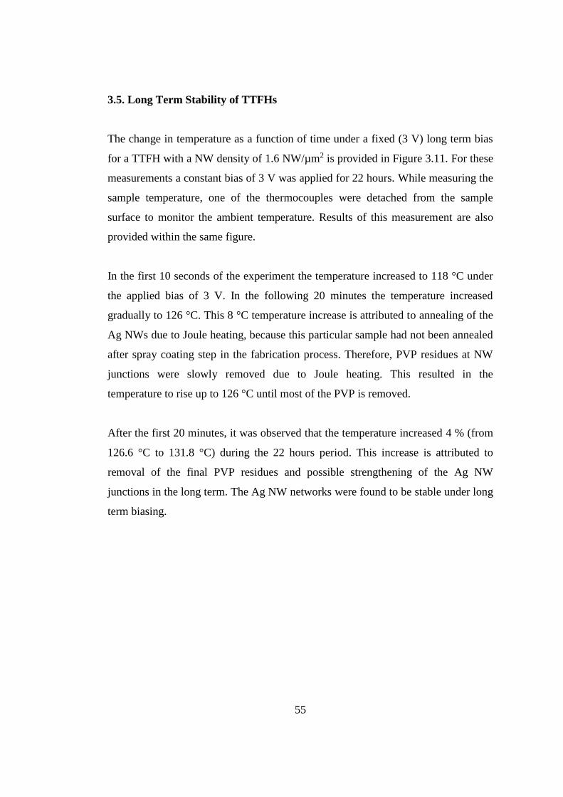
55
3.5. Long Term Stability of TTFHs
The change in temperature as a function of time under a fixed (3 V) long term bias
for a TTFH with a NW density of 1.6 NW/µm2 is provided in Figure 3.11. For these
measurements a constant bias of 3 V was applied for 22 hours. While measuring the
sample temperature, one of the thermocouples were detached from the sample
surface to monitor the ambient temperature. Results of this measurement are also
provided within the same figure.
In the first 10 seconds of the experiment the temperature increased to 118 °C under
the applied bias of 3 V. In the following 20 minutes the temperature increased
gradually to 126 °C. This 8 °C temperature increase is attributed to annealing of the
Ag NWs due to Joule heating, because this particular sample had not been annealed
after spray coating step in the fabrication process. Therefore, PVP residues at NW
junctions were slowly removed due to Joule heating. This resulted in the
temperature to rise up to 126 °C until most of the PVP is removed.
After the first 20 minutes, it was observed that the temperature increased 4 % (from
126.6 °C to 131.8 °C) during the 22 hours period. This increase is attributed to
removal of the final PVP residues and possible strengthening of the Ag NW
junctions in the long term. The Ag NW networks were found to be stable under long
term biasing.

56
3.6. Reproducibility of the TTFH Characteristics
TTFH characteristics were checked after 50 days to investigate the reproducibility
of the devices. First of all, it was found that the sheet resistance of a TTFH with a
nanowire density of 1.6 NW/µm2 increased to 4.9 Ω/sq from its initial value of 4.3
Ω/sq after 50 days. It is worth mentioning that the sample was stored in ambient
conditions within this period. Change in the temperature response for this TTFH is
given in Figure 3.12. Measurement results right after the fabrication of TTFH
devices and after 50 days of storage are plotted.
Change in the sheet resistance and therefore the thermal response was attributed to
the possible oxidation of Ag NWs under ambient conditions. Oxidation results in an
Figure 3.11. Change in temperature as a function of time for a TTFH with a
NW density of 1.6 NW/µm2 which is long term biased at 3V.

57
increase of sheet resistance of the sample, lowering the temperature attained under
an applied bias. Nevertheless, a 14% increase in the sheet resistance coupled with a
12.5% decrease in the maximum attainable temperature obtained after 50 days can
be declared as satisfactory. The performance of the Ag NW thin films even after 50
days still nearly meets the minimum standards required by industry for TCEs, T ≥
90% and Rs < 100 Ω/sq as set by Hewlett-Packard (see ref [22] of Scardaci et al.
201111).
Figure 3.12. Change in temperature as a function of time for a TTFH with a
NW density of 1.6 NW/µm2. Results for (a) right after the fabrication of
TTFH devices (Rs = 4.3 Ω/sq), and (b) after 50 days of storage (Rs = 4.9
Ω/sq), are plotted.

58
3.7. Flexibility
Effect of bending on thermal response characteristics of Ag NW networks coated on
PET substrates (4 cm x 5 cm) under an applied bias of 4 V is given in Figure 3.13. It
is observed that concave configuration under an applied bias of 4 V results in higher
attained temperatures (up to 90 °C) than those attained in straight (up to 80 °C) and
convex (up to 72 °C) configurations. Higher attained temperatures during concave
bending can be attributed to an increase in the number of physical contact points
between NWs due to an increased NW spatial density. On the other hand, convex
bending results in a decrease in NW spatial density wihch in turn decreases the
number of physical contact points.
Figure 3.13. Thermal response characteristics of Ag NW networks
coated on flexible PET substrates in straight and bended (concave
and convex) configurations under an applied bias of 4 V.

59
CHAPTER 4
CONCLUSIONS AND FUTURE WORK
4.1. Summary of the Work
There is increased interest in transparent heaters for defogging and deicing
applications. Ag NW networks are appealing candidates due to their high thermal
performance coupled with high optical transmittance. On the other hand,
conventional transparent thin film heater materials, such as ITO, have increasing
prices worldwide due to indium’s scarcity.
In this study, Ag NW networks were reproducibly deposited on different substrates.
TTFHs were fabricated through the deposisiton of Ag contacts in appropriate
geometry determined in this thesis. Effect of NW density, applied voltage and
bending on the thermal output of the TTFHs were investigated. Failure mechanism
of the TTFHs was also investigated in conjunction to the optoelectronic
characteristics of thin films.
Firstly, the effect of parallel contact geometry, 4-contact geometry and opposite
corners 2-contact geometry on the thermal characteristics of TTFHs were studied. It
was found that sharp corners having small distances in between, result in high
electrical flux and must be avoided. Therefore, TTFHs with two parallel contacts on
the opposites sides are crucial for the most homogeneous temperature distribution,
withstand higher temperatures and currents before the failure of Ag NW networks.

60
Secondly, the effect of NW density was studied. It was found that the density of
NWs can simply be increased through increasing the number of spray coating
cycles. Number of NW contacts increase with NW density, which in turn increases
the conductivity and reduces the sheet resistance. On the other hand, since there are
more NWs per unit area in a denser sample, transparency is decreased due to higher
absorption (or higher scattering) of light passing through the TTFH.
Next, the effect of bias voltage on the thermal behaviour of TTFHs with various
NW densities was investigated. It was found that the achieved maximum
temperature was 204 °C under an applied potential of 4 V for the sample with a Ag
NW density of 1.6 NW/µm2. However, this maximum temperature was not stable.
The maximum stable temperature was 180 °C under an applied bias of 9 V for the
sample with a Ag NW density of 0.6 NW/µm2. In addition to that, the sample with a
Ag NW density of 0.5 NW/µm2 reached a maximum temperature of 175 °C under
an applied bias of 11 V. All Ag NW network samples’ %T and Rs nearly meet the
minimum standards required by industry for TCEs, T ≥ 90% and Rs < 100 Ω/sq in
this work.
Next, failure mechanism of Ag NWs was investigated. As the temperature was
increased, Ag NWs began to melt and Ag began to accumulate at nanowire
junctions. Melting of thin Ag NWs resulted in Ag NWs getting even thinner. As the
temperature continued to increase, Ag NWs began to fail and rupture. This resulted
in a decrease in the number of current pathways, which began to increase the sheet
resistance of the networks upto kiloohms and then to megaohms. Finally, NWs
broke into discontinuous segments, where TTFHs failed and thermal response
droped to zero.
The effect of repetitive heating and cooling cycles on the performance of TTFHs
was studied. Thermal response was found to be almost identical in each cycle,
indicating that the structure of Ag NW networks remain intact.

61
It was also found that the Ag NW networks were stable under 22 hours long term
biasing.
Lastly, the effect of bending on the thermal response characteristics of Ag NW
networks deposited onto PET substrates was studied. It was found that attained
temperatures were higher in concave configuration compared to those attained in
straight and convex configurations.
4.2. Future Work
Spray deposited Ag NW networks can easily be scratched. This adhesion problem is
not only important because it decreases TTFH performance, but also it might bring
health concerns due to potential hazards of scratched Ag NWs. Thus a protective
coating on Ag NWs is highly desirable. Another possibility is to embed Ag NWs
into a polymeric substrate.
Oxidation/sulphidization mechanism of Ag NWs and the resulting reduction in
thermal performance of Ag NW based TTFHs may as well be investigated.
Prevention of oxidation/sulphidization again through the use of a protective coating
on Ag NWs or through embedding of Ag NWs into a polymeric substrate can also
be investigated.

62

63
REFERENCES
(1) Janas, D.; Koziol, K. K. Carbon 2013, 59, 457–463.
(2) Li, J.; Liang, J.; Jian, X.; Hu, W.; Li, J.; Pei, Q. Macromol. Mater. Eng. 2014,
299, 1403–1409.
(3) Tian, H.; Xie, D.; Yang, Y.; Ren, T.-L.; Lin, Y.-X.; Chen, Y.; Wang, Y.-F.;
Zhou, C.-J.; Peng, P.-G.; Wang, L.-G.; Liu, L.-T. Applied Physics Letters,
2011, Vol. 99, No. 25, 253507.
(4) Celle, C.; Mayousse, C.; Moreau, E.; Basti, H.; Carella, A.; Simonato, J.-P.
Nano Research 2012, Vol. 5 No. 6, 427-433.
(5) Gordon R.G. MRS Bulletin 2000, 52-57.
(6) Honeywell Sensing and Control Application Note,
www.honeywell.com/sensing (accessed July 20, 2015).
(7) Volman, V.; Zhu, Y.; Raji, A.-.O.; Genorio, B.; Lu, W.; Xiang, C.; Kittrell,
C.; Tour, J. M. ACS Appl. Mater. Interfaces 2014, 6, 298−304.
(8) Liu, C. -H.; Yu, X. Nanoscale Research Letters 2011, 6, 75.
(9) Minco, “Flexible Heaters Design Guide”, HDG01(A).
(10) Minco, Thermofoil™ Heaters, Bulletin HS-202(B).
(11) Scardaci V.; Coull R.; Lyons P.E.; Rickard D.; Coleman J.N. Small 2011, 7,
No. 18, 2621–2628.
(12) Facchetti, A.; Marks, T. J. “Transparent Electronics: From Synthesis to
Applications”, 2010, John Wiley & Sons Ltd, Chapter 2 “Transparent Oxide
Semiconductors: Fundamentals and Recent Progress”, H. Hosono.
(13) Sorel, S.; Bellet, D.; Coleman, J.N.; ACS Nano 2014, vol. 8, no 5, 4805–4814.
(14) Yakuphanoglu, F.; Anand, R.S. Syn. Met. 2010, vol. 160, no. 21, 2250–2254,.
(15) AEI August 2014, Dempa Publications, Inc., Tech Focus, “Best-in-Class
Touchscreens with Silver Nanowires”.

64
(16) http://www.eizoglobal.com/library/basics/
basic_understanding_of_touch_panel/ (accessed July 20, 2015).
(17) Kiruthika, S.; Gupta, R.; Kulkarni, G. U. RSC Adv. 2014, 4, 49745–49751.
(18) Kwon, N.; Kim, K.; Heo, J.; Yi, I.; Chung, I. Nanotechnology 2014, 25,
265702.
(19) Kim, T. Y.; Kim, Y. W.; Lee, H. S.; Kim, H.; Yang, W. S.; Suh, K. S. Adv.
Funct. Mater. 2013, 23, 1250–1255.
(20) Gupta, R.; Rao, K. D. M.; Srivastava, K.; Kumar, A.; Kiruthika, S.; Kulkarni,
G.U. Appl. Mater. Interfaces 2014, 6, 13688−13696.
(21) Wang, S.; Zhang, X.; Zhao, W. Journal of Nanomaterials 2013, 2013,
456098.
(22) Zhang, X., Yan, X., Chen, J., Zhao, J. Carbon 2014, 69, 437–443.
(23) Kim, D., Zhu L., Jeong, D. -J., Chun, K., Bang, Y. -Y., Kim, S. -R., Kim, J. -
H., Oh, S. -K. Carbon 2013, 63, 530–536.
(24) Cheong, H.-G.; Song, D.-W.; Park, J.-W. Microelectron. Eng. 2015, 146, 11–
18.
(25) Ji, S.; He, W.; Wang, K.; Ran, Y.; Ye, C.; Small 2014.
(26) Hsu, P.-C.; Liu, X.; Liu, C.; Xie, X.; Lee, H.R.; Welch, A.J.; Zhao, T.; Cui,
Y. Nano Lett. 2015, 15, 365−371.
(27) Rao, K. D. M.; Kulkarni, G. U. Nanoscale 2014, 6, 5645–5651.
(28) Janas, D.; Koziol, K. K. JOACE 2014, 2, 150.
(29) Jang, H.-S.; Jeon, S. K.; Nahm, S. H. Carbon 2011, 49, 111–116.
(30) Jung, D.; Kim, D.; Lee, K. H.; Overzet, L. J.; Lee, G. S. Sensors and
Actuators A 2013, 199, 176– 180.
(31) Kang, T. J.; Kim, T.; Seo, S. M.; Park, Y.J.; Kim, Y. H. Carbon 2011, 49,
1087–1093.

65
(32) Kim, D.; Lee, H. -C.; Woo, J. Y.; Han, C. -S. J. Phys. Chem. C 2010, 114,
5817–5821.
(33) Kim, D.; Lee, H. -C.; Woo, J. Y.; Han, C.-S. Proceedings of 10th IEEE
International Conference on Nanotechnology, Joint Symposium with Nano
Korea 2010.
(34) Wu, Z. P.; Wang, J.N. Physica E 2009, 42, 77–81.
(35) Yoon, Y.-H.; Song, J.-W.; Kim, D.; Kim, J.; Park, J.-K.; Oh, S.-K.; Han C.-
S.; Adv. Mater. 2007, 19, 4284–4287.
(36) Bae, J. J.; Lim, S. C.; Han, G. H.; Jo, Y. W.; Doung, D. L.; Kim, E. S.; Chae,
S. J.; Huy, T. Q.; Luan, N. V.; Lee, Y. H. Adv. Funct. Mater. 2012, 22, 4819–
4826.
(37) Kang, J.; Kim, H.; Kim, K.S.; Lee, S.-K.; Bae, S.; Ahn, J.-H.; Kim, Y.-J.;
Choi, J.-B.; Hong, B.H. Nano Lett. 2011, 11, 5154–5158.
(38) Lee, B.-J.; Jeong, G.-H. Current Applied Physics 2012, 12, 113-117.
(39) Wang, J.; Fang, Z.; Zhub, H.; Gao, B.; Garner, S.; Cimo, P.; Barcikowski, Z.;
Mignerey, A.; Hub, L. Thin Solid Films 2014, 556, 13–17.
(40) Im, K.; Cho, K.; Kim, J.; Kim, S. Thin Solid Films 2010, 518, 3960–3963.
(41) Yang, K.; Cho, K.; Im, K.; Kim, S. Materials Research Bulletin 2015, 63,
194–198.
(42) Ahn, B.D.; Oh, S.H.; Hong, D.U.; Shin, D.H.; Moujoud, A.; Kim, H. J.
Journal of Crystal Growth 2008, 310, 3303–3307.
(43) Kim, J. H.; Ahn, B. D.; Kim, C. H.; Jeon, K. A.; Kang, H. S.; Lee, S. Y. Thin
Solid Films 2008, 516, 1330–1333.
(44) Li J.; Liang J.; X. Jian; W. Hu; J. Li; Qibing Pei Macromol. Mater. Eng.
2014, 299, 1403–1409.
(45) Calnan, S.; Tiwari, A.N. Thin Solid Films 2010, 518, 1839–1849.
(46) Chopra, K.L., Major, S., Pandya, D.K. Thin Solid Films 1983, 102, 1.

66
(47) Minami, T.; Miyata, T., Presentation given at SPIE 2008, January 23rd.
(48) Liu, H.; Avrutin, V.; Izyumskaya, N.; Özgür, Ü.; Morkoç H. Superlattices
and Microstructures 2010, 48, 458–484.
(49) Wager, J. F.; Keszler, D. A.; Presley, R. E. Transparent Electronics, 2008,
Springer.
(50) http://www.tibtech.com/conductivity.php (accessed July 20, 2015).
(51) Bellingham, J. R.; Phillips, W. A.; Adkins, C. J. J Mater Sci Lett 1992, 11,
263-265
(52) Kawazoe, H.; Yasukawa, M.; Hyodo, H.; Kurita, M.; Yanagi, H.; Hosono, H.
Nature 1997, 389, 939-942.
(53) Rupperecht, G. Z. Phys. 1954, 139, 504.
(54) Tuna, O.; Selamet, Y; Aygun, G.; Ozyuzer, L. J. Phys. D: Appl. Phys. 2010,
43, 055402.
(55) Khaligh, H. H., Silver Nanowire Transparent Electrodes: Fabrication,
Characterization, and Device Integration, (Thesis, M.S.), Electrical and
Computer Engineering –Nanotechnology, University of Waterloo, 2013.
(56) Cairns, D.R.; Witte, R.P.; Sparacin, D.K.; Sachsman, S.M.; Paine, D.C.;
Crawford, G.P.; Newton, R.R. Appl. Phys. Lett. 2000, 76, 1425.
(57) Sui, D.; Huang, Y.; Huang, L.; Liang, J.; Ma, Y.; Chen, Y. Small 2011, 7,
3186.
(58) Wang, X.; Zhi, L.; Muellen, K. Nano. Lett. 2008, 8, 323.
(59) Sayers, S. A.; Gagiano, M. A.; Moore, T. D. Patent Cooperation Treaty
(PCT) WO 2010/131050 A1
(60) Sylvain, T. US006341554B2.
(61) Kawashima, T.; Ezure, T.; Okada, K.; Matsui, H.; Goto, K.; Tanabe, N. J.
Photochem. Photobiol. A 2004,164, 199–202.
(62) Bae, J.W.; Lee, S.W.; Yeom, G.Y. Electrochem. Soc. 2007, 154, D34–D37.
67
(63) Elmer, K. J. Phys., D, Appl. Phys. 2001, 34, 3097.
(64) Agura, H.; Suzuki, H.; Matsushita, T.; Aoki, T.; Okuda, M. Thin Solid Films
2003, 445, 263–267.
(65) Park, S.-M.; Ikegami, T.; Ebihara, K. Thin Solid Films 2006, 513, 90–94.
(66) Ohta, H.; Orita, M.; Hirano, M.; Tanji, H.; Kawazoe, H.; Hosono, H. Appl.
Phys. Lett. 2000,76, 2740–2742.
(67) Qadri, S. B.; Kim, H., Khan, H. R., Pique, A.; Horowitz, J. S.; Chrisey, D.;
Kim, W. J.; Skelton, E. F. Thin Solid Films 2000, 377–378, 750–754.
(68) Kim, H.; Gilmore, C. M.; Horwitz, J. S.; Pique, A.; Murata, H.; Kushto, G.
P.; Schlaf, R.; Kafa, Z. H.; Chrisey, D. B. Appl. Phys. Lett. 2000, 76, 259–
261.
(69) Iijima, S. Nature 1991, 56, 354.
(70) Chen, K.-R.; Yeh, H.-F.; Chen, H.-C.; Liu, T.-J.; Huang, S.-J.; Wu, P.-Y.;
Tiu, C. Advances in Chemical Engineering and Science 2013, 3, 105-111.
(71) Nirmalraj, P. N.; Lyons, P. E.; De, S.; Coleman, J. N.; Boland, J. J. Nano
Lett. 2009, 9, 3890 .
(72) https://en.wikipedia.org/wiki/Graphene (accessed July 25, 2015).
(73) Lupu, N. “Nanowires Science and Technology” 2010, Intech.
(74) De, S.; Higgins, T.; Lyons, P. E.; Doherty, E. M.; Nirmalraj, P. N.; Blau, W.
J.; Boland, J. J.; Coleman, J. N. ACS Nano 2009, 3, 1767.
(75) http://www.digitimes.com/news/a20140415VL200.html (accessed July 20,
2015).
(76) Langley, D.; Giusti, G.; Mayousse, C.; Celle, C.; Bellet, D.; Simonato, J.-P.
Nanotechnology 2013, 24, 452001.
(77) Langley, D. P.; Lagrange, M.; Giusti, G.; Jiménez, C.; Bréchet, Y.; Nguyenb,
N. D.; Bellet, D. Nanoscale 2014, 6, 13535.

68
(78) De, S.; Higgins, T. M.; Lyons, P. E.; Doherty, E. M.; Nirmalraj, P. N.; Blau
W. J.; Boland, J. J.; Coleman, J. N. ACS Nano 2009, 3, 1767-1774.
(79) Kholmanov, I. N.; Stoller, M. D.; Edgeworth, J.; Lee, W. H.; Li, H.; Lee, J.;
Barnhart, C.; Potts, J. R.; Piner, R.; Akinwande, D.; Barrick, J. E.; Ruoff, R.
S. ACS Nano 2012, 6, 6, 5157–5163.
(80) Chen, T. L.; Ghosh, D. S.; Mkhitaryan, V.; Pruneri, V. ACS Appl. Mater.
Interfaces 2013, 5, 11756−11761.
(81) Choi, K. -H.; Kim, J.; Noh, Y. -J.; Na, S. -I.; Kim, H.-K. Solar Energy
Materials & Solar Cells 2013, 110, 147–153.
(82) Koo, B. –R.; Ahn, H. –J. Applied Physics Express 2014, 7, 075002.
(83) Golobostanfard, M. R.; Abdizadeh, H.; Mohammadi, S.; Baghchesara, M. A.
Solar Energy Materials & Solar Cells 2015, 132, 418–424.
(84) Rathmell, A. R.; Nguyen, M.; Chi, M.; Wiley, B. J. Nano Lett. 2012, 12,
3193−3199.
(85) Jeong, C.; Nair P.; Khan, M.; Lundstrom, M.; Alam, M. A. Nano Lett. 2011,
11, 5020–5025.
(86) Kumar, A. B. V. K.; Bae, C.; Piao, L.; Kim, S. -H. Materials Research
Bulletin 2013, 48, 2944–2949.
(87) Haacke, G. J. Appl. Phys. 1976, 47, 4086.
(88) Pichitpajongkit, A.; Lee J.; Eom, H.; Yang, D.; Yoon, J.; Lee, J.; Park, I.;
“Joule Heating and Thermal Analysis of Silver Nanowire Random
Network”,.
(89) Ragab, T.; Basaran, C. J. Appl. Phys 2009, 106, 063705.
(90) Rutherglen, C.; Burke, P. J. Small 2009, 5, 884–906.
(91) Tsuchiya, K.; Li, Y.; Saka, M. Nanoscale Research Letters 2014, 9, 239.
(92) Toimil Molares, M. E.; Balogh, A. G.; Cornelius, T. W.; Neumann R.;
Trautmann C. Appl. Phys. Lett. 2004, 85, 5337.

69
(93) Jeong, W.; Kim, K.; Kim, Y.; Lee, W.; Reddy, P. Scientific Reports 2014 4,
4975.
(94) Black, J. R. IEEE Transactions on Electron Devices 1969, 4, 338-347.
(95) Kim, S. H.; Choi, B. S.; Kang, K.; Choi, Y. S.; Yang, S. I. J. Alloys Compd.
2007, 433, 261.
(96) Grijalva, A. S.; Urbina, R. H.; Silva, J. F. R.; Borja, M. A.; Barraza, F. F. C.;
Amarillas, A. P. Physica E 2005, 25, 438.
(97) Mazur, M. Electrochem. Commun. 2004, 6, 400.
(98) Huang, L. M.; Wang, H. T.; Wang, Z. B.; Mitra, A; Bozhilov, K. N.; Yan, Y.
S. Adv. Mater. 2002, 14, 61.
(99) Xu, J.; Hu, J.; Peng, C. J.; Liu, H. L.; Hu, Y. J. Colloid Interface Sci. 2006,
298, 689.
(100) Wang, Z.; Liu, J.; Chen, X.; Wan, J.; Qian, Y Chem.—Eur. J. 2005, 11, 160.
(101) Zhou, Y.; Yu, S.; Wang, C.; Li, X.; Zhu, Y.; Chen, Z. Adv. Mater. 1999, 11,
850.
(102) Zou, K.; Zhang, X. H.; Duan, X. F.; Meng, X. M.; Wu, S. K. J. Cryst. Growth
2004, 273, 285.
(103) Braun, E.; Eichen, Y.; Sivan, U.; Yoseph, G. B. Nature 1998, 391, 775.
(104) Keren, K.; Krueger, M.; Gilad, R.; Ben-Yoseph, G.; Sivan, U.; Braun, E.
Science 2002, 297, 72.
(105) Berchmans, S.; Nirmal, R. G.; Prabaharan, G.; Madhu, S.; Yegnaraman, V. J.
Colloid Interface Sci. 2006, 303, 604.
(106) Kong, L. B.; Lu, M.; Li, M. K.; Li, H. L.; Guo, X. Y. J. Mater. Sci. Lett.
2003, 22, 701.
(107) Piquemal, J. Y.; Viau, G.; Beaunier, P.; Verduraz, F. B; Fievet, F. Mater. Res.
Bull. 2003, 38, 389.

70
(108) Gasga, J. R.; Elechiguerra, J. L.; Liu, C.; Bragado, A. C.; Carrizales, J. M.
M.; Yacaman, M. J. J. Cryst. Growth 2006, 286, 162.
(109) Coskun, S.; Aksoy, B.; Unalan, H.E. Cryst. Growth Des. 2011, 11, 4963–
4969.
(110) Fievet, F.; Lagier, J. P.; Blin, B.; Beaudoin, B.; Figlarz, M. Solid State Ionics
1989, Vol. 32, No. 3, 198-205.
(111) Fievet, F.; Lagier, J. P.; Figlarz, M. MRS Bull. 1989, 14, 29.
(112) Viau, G.; Fievet-Vincent, F.; Fievet, F. Solid State Ionics 1996, 84, 259.
(113) Toneguzzo, G.; Viau, O.; Acher, F.; Fievet-Vincent, F.; Fievet, F. Adv.
Mater. 1998, 10, 1032.
(114) Bonet, F.; Delmas, V; Grugeon, S.; Urbina, R. H.; Silvert, P. Y.; Tekaia-
Elhsissen, K. Nanostruct. Mater. 1999, 11, 1277.
(115) Wiley, B.; Sun, Y. G.; Mayers, B.; Xia, Y. N. Chemistry-A European Journal
2005, Vol. 11, No. 2, 454-463.
(116) Zang, Z.; Zhao, B.; Hu, L. J. Solid State Chem. 1996, 121, 105.
(117) Roosen, A. R.; Carter, W. C. Physica A 1998, 232, 261.
(118) Liu, C. -H.; Yu, X. Nanoscale Res. Lett. 2011, 6, 75–82.
(119) Deegan, R. D.; Bakajin, O.; Dupont, T. F.; Huber, G.; Nagel, S. R.; Witten, T.
A. Nature 1997, 389, 827-829.
(120) Kim, T.; Canlier, A.; Kim, G. H.; Choi, J.; Park, M.; Han, S. M. ACS Appl.
Mater. Interfaces 2012, 5, 788−794.
(121) Hauger, T. C.; Al-Rafia, S. M. I.; Buriak, J. M. ACS Appl. Mater. Interfaces
2013, 5, 12663−12671.
(122) Kaempgen, M.; Lebert, M.; Haluska, M.; Nicoloso, N.; Roth, S. Adv. Mater.
2008, 20, 616–620.
71
(123) Tenent, R. C.; Barnes, T. M.; Bergeson, J. D.; Ferguson, A. J.; To, B.;
Gedvilas, L. M.; Heben, M. J.; Blackburn, J. L. Adv.Mater. 2009, 21, 3210–
3216.
(124) Park, J. W.; Shin, D. K.; Ahn, J.; Lee, J. Y. Semicond. Sci. Technol. 2014, 29,
015002.
(125) Preston, C.; Xu, Y.; Han, X.; Munday, J. N.; Hu, L. Nano Res. 2013, 6, 461–
468.
(126) Coskun, S.; Ates, E. S.; Unalan, H. E. Nanotechnology 2013, 24, 125202.
(127) Coskun, S. Synthesis of Silver Nanowires Through Polyol Process, (Thesis,
M.S.), Department of Materials Science and Engineering Middle East
Technical University, 2012.