Embed Size (px)
Citation preview

Fourier Optics and Optical Diagnostics Laboratory
Transport Modeling of Multiple-Quantum-Well Optically
Addressed Spatial Light Modulators
A Dissertation Submitted to the Department of Physics
Stanford University
nVC
r^fcj
Stephen Lee Smith
December 1996
88B$QXLm OraPECTBD. Dtesdtoutiaa Unlimited

Transport Modeling of Multiple-Quantum-Well Optically
Addressed Spatial Light Modulators
A DISSERTATION
SUBMITTED TO THE DEPARTMENT OF PHYSICS
AND THE COMMITTEE ON GRADUATE STUDIES
OF STANFORD UNIVERSITY
IN PARTIAL FULFILLMENT OF THE REQUIREMENTS
FOR THE DEGREE OF
DOCTOR OF PHILOSOPHY
Stephen Lee Smith
December 1996

© Copyright by Stephen Lee Smith 1996
All Rights Reserved

I certify that I have read this dissertation and that in my opinion it is fully adequate, in scope and quality, as a dissertation for the degree of Doctor of Philosophy.
Lambeitps Hesselink (Principal Adviser)
I certify that I have read this dissertation and that in my opinion it is fully adequate, in scope and quality, as a dissertation for the degree of Doctor of Philosophy.
1 m^c/^ Steven Chu
I certify that I have read this dissertation and that in my opinion it is fully adequate, in scope and quality, as a dissertation for the degree of Doctor of Philosophy.
■oA-hcfK Martin Fejer
Approved for the University Committee on Graduate Studies:
in

Abstract
Optically addressed spatial light modulators are essential elements in any optical process-
ing system. Applications such as optical image correlation, short pulse auto-correlation,
and gated holography require high speed, high resolution devices for use in compact, high
throughput systems. Other important device criteria include ease of fabrication and opera-
tion. In this work we study the transport dynamics of a new kind of optically addressed
spatial light modulator that uses semi-insulating or intrinsic quantum-well material to pro-
duce high performance devices without the need for pixellation or complicated device
design.
In response to an incident intensity pattern, basic device operation occurs through the
screening of an applied voltage via the optical generation, transport, and trapping of pho-
tocarriers. A field pattern which mimics the incident intensity pattern is produced by the
screening process. This generates strong index and absorption holograms via the quantum
confined Stark effect. These holograms can be read out simultaneously with a probe beam
to provide dynamic read/write operation.
Overall device performance is determined by the transport of photocarriers during the
field screening process. We have developed a transient, two-dimensional drift-diffusion
model to describe both free and well-confined carrier transport as well as nonlinear effects
such as velocity saturation and field-dependent carrier emission from quantum wells. Var-
ious analytical and numerical results for the internal carrier and space charge distributions,
different screening regimes, and relative carrier contributions to the screening process are
given. An experimental characterization of a GaAs/AlGaAs device using optical
IV

transmission and photocurrent techniques is also presented and used to verify the main
results of the transport model.
Analytical and numerical analyses of various transport effects that limit the resolution
are also given. We show that, contrary to the results of earlier device models, both the
speed response and resolution can be simultaneously optimized using appropriate device
design. Using realistic device parameters, frame rates of 100 kHz at 10 mW/cm2 intensity
with 7 \im device resolution are predicted.

Acknowledgments
First, I would like to thank my advisor, Bert Hesselink, for his support and encouragement
over these past several years. He gave me a great deal of freedom not only in choosing this
topic, but in determining the course of research. He has allowed me to pursue a number of
interests, both directly and not so directly, related to this project. It is an opportunity that I
have greatly appreciated. I would also like to thank two researchers from AT&T Bell Lab-
oratories who have been of great help: William Coughran who got me started on semicon-
ductor device modeling, and Afshin Partovi who fabricated and generously provided the
samples used in our experiments.
One of the great things about being in a group as large as ours is that there are always
interesting and useful people around. I would especially like to thank Jeff Wilde who first
showed me around the lab during my first year in the group, and Lew Aronson who
pointed me towards this project. I would also like to thank Elizabeth Downing for her aid
in getting a Ti:S laser system up and running. As this research involved intensive computer
simulations, it would not have been possible without the help of the following very gener-
ous and very good computer people: Jim Helman, Paul Ning, Mark Peercy, Thierry
Delmarcelle, Yuval Levy, and Raj Batra. I would also like to thank some of my lab and
office mates for their friendship and good conversations over the years, especially Muthu
Jeganathan, John "Q-function" Heanue, and Raymond DeVre. Special thanks goes to our
group secretary, Lilyan Sequeria, for her great efficiency and friendly dealings as she bat-
tled the Stanford paperwork jungle.
VI

Finally, I would like to thank my family for their support and encouragement of my
work and interest in science- not only here at Stanford, but all during secondary school,
through the science fair projects, and at Florida. I would also like to thank my Swedish
clan for their support and sometimes overly zealous, but very much appreciated, interest in
my work.
Last (but really first!), I would like to thank my wife Monica who has been extremely
supportive, and who has graciously put up with too many late nights and too many absent
Sundays.
This research has been partially supported by the Office of Naval Research, and the
Advanced Research Projects Agency through the CNOM program.
vii

Contents
Abstract iv
Acknowledgments vi
List of Tables xii
List of Figures xiii
1 Introduction 1
1.1 Background on the MQW-OASLM 2
1.2 Thesis Overview 4
2 Optically Addressed Spatial Light Modulators 6
2.1 Basic Device Designs 7
2.1.1 Photoconductive/Electro-optic Devices 7
2.1.2 PROM 8
2.1.3 Quantum-Well Modulators 9
2.2 MQW-OASLM 11
2.3 Diffraction 13
2.3.1 Raman-Nath Diffraction 14
2.3.2 Holography 16
2.4 Application Example: Optical Correlator 18
2.5 Performance Comparison 21
Vlll

2.6 Summary 22
3 Optical and Transport Properties of Multiple-Quantum- Wells 25
3.1 Electronic Structure 26
3.2 Optical Properties 30
3.2.1 Excitons 30
3.2.2 Quantum Confined Stark Effect 32
3.2.3 Electro-optic Effect 34
3.3 Transport Properties 35
3.3.1 Vertical vs. In-plane 35
3.3.2 Escape Mechanisms 37
3.3.3 Shallow Trap Model 41
3.4 Summary 43
4 Electric Field Screening 44
4.1 Device Model 45
4.2 Carrier Distributions 49
4.3 Injection Model 53
4.4 Field Screening 54
4.4.1 Short Drift Lengths 55
4.4.2 Long Drift Lengths .56
4.4.3 Initial Rate 58
4.5 Numerical Results 59
4.6 Semiconductor and Quantum-Well Effects 61
4.7 Summary 65
5 Transmission and Photocurrent Response 66
5.1 Experiment 67
5.1.1 Setup 68
5.1.2 Transmission Results 70
IX

5.1.3 Photocurrent Results 73
5.2 Simulation 75
5.2.1 Device Model 75
5.2.2 Field Screening Results 77
5.2.3 Photocurrent Results 78
5.3 Summary 83
5.4 Appendix 83
Grating Formation 86
6.1 Device Model 87
6.2 Small Signal Injection Model 90
6.2.1 Electrostatics 91
6.2.2 Carrier Distributions 93
6.2.3 Grating Formation 96
6.3 Numerical Results 99
6.3.1 Field Uniformity 99
6.3.2 Intensity Modulation Dependence 100
6.3.3 Transverse Transport 103
6.4 Summary 104
Resolution Performance 106
7.1 Transverse Transport 107
7.1.1 Interior Transport 108
7.1.2 Surface Transport 112
7.1.3 Resolution Estimates 113
7.1.4 Intensity Modulation Dependence 113
7.2 Semiconductor and Quantum-Well Effects 115
7.3 Optimization Example 117
7.4 Summary 120

8 Conclusions 122
8.1 Summary of Contributions 122
8.2 Suggestions for Future Research 124
A Numerical Methods 126
B Publications 131
Bibliography 132
XI

List of Tables
2-1 OASLM performance parameters 22
4-1 Device parameters for ID simulations . . . .59
4-2 Velocity saturation model 62
5-1 Simulation parameters for comparison with experiments 76
7-1 Estimated resolution limits 114
7-2 Optimization parameters 117
xn

List of Figures
1-1 Device technology leading to the MQW-OASLM 2
2-1 Photoconductive/electro-optic modulator design 8
2-2 Pockels readout optical modulator design 9
2-3 Quantum-well modulators 10
2-4 MQW-OASLM design 12
2-5 AT&T device structure 13
2-6 Raman-Nath diffraction 14
2-7 Holography in a MQW-OASLM 17
2-8 Optical correlator 19
2-9 OASLM bit rate and intensity comparison 23
3-1 Band diagram of GaAs 27
3-2 Quantum-well band edges 28
3-3 Quantum-well subbands 29
3-4 Absorption spectrum of a GaAs/AlGaAs MQW device 31
3-5 Quantum confined Stark effect 33
3-6 The electro-optic effect produced by the QCSE 34
3-7 Vertical and in-plane quantum-well transport 36
3-8 Thermionic and tunneling escape from a quantum well 37
3-9 Escape rates for electrons and holes 40
3-10 Shallow trap model for quantum wells 42
xni

4-1 ID device geometry 46
4-2 Quasi-steady state carrier distributions 52
4-3 Injection model of screening 53
4-4 Screening of the internal field 57
4-5 Initial screening rate 58
4-6 Interior field distribution 60
4-7 Comparison of the injection model and full numerical solutions 61
4-8 Field screening for constant and velocity-saturated mobilities 63
5-1 Experimental setup for measuring transmission and photocurrent 69
5-2 QCSE transmission 71
5-3 Measured screening of the electric field 72
5-4 Measured photocurrent for various applied voltages 74
5-5 Measured photocurrent for both polarities 75
5-6 Simulated field screening using constant mobilities 78
5-7 Simulated photocurrent using constant mobilities 79
5-8 Simulated photocurrent for both polarities using constant mobilities 80
5-9 Simulated photocurrent using velocity-saturated mobilities 81
5-10 Simulated photocurrent for both polarities using velocity-saturated mobilities . 82
5-11 Amplifier schematics 84
6-1 2D device geometry 88
6-2 Grating formation 90
6-3 Dynamics of the first-order field component 98
6-4 Interior distribution of the first-order field component 100
6-5 Grating dependence on the intensity modulation 101
6-6 Geometric and nominal resolution curves 104
7-1 Resolution limit imposed by transverse interior diffusion 110
7-2 Resolution limit imposed by transverse interior drift Ill
xiv

7-3 Resolution limit imposed by transverse surface diffusion and drift 112
7-4 Resolution dependence on the intensity modulation 115
7-5 Optimized and non-optimized resolution curves 119
7-6 Resolution limits for various transport mechanisms 120
A-l Simulation grid 127
A-2 Adaptive time step control 129
xv

Chapter 1
Introduction
Optical processing systems combine the inherent parallelism of optics with the square-law
intensity response of optically addressed spatial light modulators to perform high speed,
page-based computations. Applications include optical image correlation [1], short pulse
auto-correlation [2], and gated holography [3]. Compact, high speed systems require opti-
cally addressed spatial light modulators with high spatial resolution and fast frame rates.
Many devices, such as the Pockels Readout Optical Modulator (PROM) [4] and the liquid
crystal light valve [5], have been developed over the years. However, none of these devices
has simultaneously demonstrated the following requirements that are needed in most
applications: high speed, high resolution, gray scale response, low power operation, low
applied voltage, convenient operating wavelength, and easy fabrication.
The insulator/multiple-quantum-well/insulator devices first developed at AT&T Bell
Laboratories in 1991 have the potential to meet many of these requirements [6]. These
devices are commonly referred to as multiple quantum well optically addressed spatial
light modulators (MQW-OASLM) or Stark-geometry photorefractive quantum well
devices. They combine the fast carrier transport and large electro-optic response of quan-
tum wells with a thin, layered structure to produce many of the properties described above.
The optimization of both the speed and resolution performance, however, has been ham-
pered by a lack of understanding of the details of device operation, and, specifically, the

Introduction
PROM I Geometry I
Photorefractive Semiconductors
Speed Quantum Wells
Electro-optics
MQW-OASLM
Figure 1-1 Three device technologies led to the development of the MQW-OASLM. The sand- wich style geometry was taken from the PROM. The use of semiconductor material to obtain fast photoconductive response rates was taken from photorefractive research. Large, resonant electro-optic effects are obtained by using semiconductor quantum wells. The sketch of the device structure shows the interior photoconductive layer surrounded by insulating layers and transparent electrodes.
role of the quantum wells. Addressing these issues is one of the main motivations for this
work.
1.1 Background on the MQW-OASLM
As diagrammed in Fig. 1-1, the development of the multiple-quantum-well optically
addressed spatial light modulator originated from three different device technologies over
three decades. The basic device structure was taken from the PROM, one of the first opti-
cally addressed spatial light modulators developed in the 1970's [4]. This device uses a
photorefractive crystal of bismuth-silicon-oxide (BSO) sandwiched between two insulat-
ing parylene layers. The BSO layer acts both as a photoconductor and as an electro-optic
modulator. A uniform voltage is applied by transparent electrodes. Device operation pro-
ceeds via the transport of photogenerated carriers created by a writing intensity pattern.
The trapping of photogenerated carriers in midgap traps produces a space charge that
screens the applied voltage in a pattern that mimics the writing image. Subsequent

3 CHAPTER 1
electro-optic modulation by the linear Pockels effect creates a corresponding phase pat-
tern that can be read out with another optical beam.
A number of device models were developed to analyze the resolution performance of
various assumed space-charge distributions, and some simple transport models were even
constructed [7-10]. The overall device performance was fairly modest, and the applied
voltage requirements were quite high, ~1 kV. The advent of liquid crystal devices in the
early 1980's with equivalent frame rates and much lower voltage requirements quickly
doomed the PROM.
Some of the performance limitations of the PROM arose from the use of a thick
(-300 |im) oxide photorefractive material. This thickness was required to produce signifi-
cant phase modulation from the relatively weak linear electro-optic effect. The long device
length combined with the inherently poor transport properties of oxide materials to pro-
duce slow response rates. In addition, the electrostatics of the extended space charge lim-
ited the resolution to a poor -10 lp/mm, and convenient, IR wavelengths could not be
used.
In the 1980's, work began on using resonant electro-optic effects in bulk semiconduct-
ing photorefractives as a way of combining a stronger electro-optic effect with the fast
transport properties of semiconductors [11]. This work was primarily aimed at improving
photorefractive phase conjugators, but it soon became apparent that large, resonant elec-
tro-optic effects could be used to replace the relatively weak Pockels effect in semiconduc-
tors for various types of photorefractive applications. Device operation was also
compatible with diode lasers.
Around the same time, independent developments were being made in using quantum-
well structures as electro-optic modulators [12]. By 1985, Miller et al. at AT&T Bell Lab-
oratories established the quantum confined Stark effect as a very effective, although qua-
dratic, electro-optic effect [13]. To take advantage of this electro-optic effect, however, the
electric field had to be applied perpendicular to the layers- exactly the same geometry as in
the PROM. In 1991, Partovi et al. revived the PROM geometry and began using multiple-
quantum-wells as the active photoconductive and electro-optic layer [6]. Due to the very

Introduction 4
large index of refraction and absorption changes produced by the quantum confined Stark
effect, large phase and amplitude modulation can be produced in thin (~2 |im) quantum-
well layers. This allows the construction of very compact structures that offer low voltage
operation and suppressed electrostatic limitations on the resolution. In fact, in the MQW-
OASLM the two fundamental aspects of device performance, speed and resolution, are
determined primarily by carrier transport during the screening of the applied field.
Since the initial demonstration of a MQW-OASLM in 1991, only a handful of device
models have been developed to describe basic device operation and simple image
formation [14, 15,16]. Typically, ad hoc or highly restrictive assumptions are invoked to
allow simple analytical or numerical solutions. At a minimum, a two-dimensional, tran-
sient device model that is capable of handling highly nonlinear and dynamic carrier trans-
port is required. To date, no such model has been presented. In addition, no model has
explicitly considered bipolar transport or the role of quantum wells in determining the res-
olution and speed performance.
1.2 Thesis Overview
The bulk of this thesis involves the development, solution, and understanding of a com-
plete, two-dimensional device model to describe device operation and establish the perfor-
mance limits of a MQW-OASLM. Before addressing these topics directly, however, we
begin in Chapter 2 with a general description of optically addressed spatial light modula-
tors including examples of different types of devices and applications. A comparison of
the performance of various photoconductive OASLM's indicates that the MQW-OASLM
has the potential to have the best combination of speed and resolution performance within
its class. One of the reasons for this success is the very large, resonant electro-optic effect
produced by quantum confinement in the quantum wells. This effect, known as the quan-
tum confined Stark effect, is reviewed in Chapter 3. Carrier transport in quantum wells is
also discussed, and a shallow trap model that allows the inclusion of quantum wells in
standard semiconductor transport models is presented.

5 CHAPTER 1
The discussion of carrier transport modeling begins in Chapter 4 where a drift-diffu-
sion model is developed to describe device operation under uniform illumination. This
one-dimensional device model is used to construct a detailed description of the screening
process and to identify basic operating regimes. Techniques for optimizing the speed
response are also given. Frame rates of 100 kHz at 10 mW/cm2 intensity are predicted.
The experimental characterization of a GaAs/AlGaAs device is then described in
Chapter 5. Optical transmission and photocurrent measurements are used to probe the
basic screening behavior under uniform illumination. The photocurrent measurement in
particular is shown to provide a sensitive probe of the screening dynamics. A comparison
of the measured screening behavior with the transport model developed in Chapter 4
shows very good agreement.
A simple case of image formation using sinusoidal gratings is then studied in
Chapters 6 and 7 using a 2D device model which incorporates both free and quantum-well
transport. The dynamics of grating formation, the role of vertical and transverse carrier
transport in limiting the resolution, and some nonlinear transport effects in semiconduc-
tors and quantum wells are discussed. An optimization example which describes tech-
niques to simultaneously optimize both the speed and resolution performance is also
given. Device resolutions of 7 U.m are obtained using realistic device parameters while
maintaining a 100 kHz frame rate at 10 mW/cm2 intensity.

Chapter 2
Optically Addressed Spatial Light Modulators
The primary function of an optically addressed spatial light modulator (OASLM) is to
convert an input image into a corresponding refractive index and absorption pattern. Sub-
sequent readout by another optical beam transfers the optical modulation pattern onto the
amplitude and phase of the readout beam. The square-law intensity response of most
OASLM's, combined with optical readout, produces devices suitable for many optical
processing applications such as optical correlation and spatial filtering. OASLM's can also
replace standard film in general holographic systems.
The OASLM label is usually reserved for so-called dynamic devices. Unlike photo-
graphic film, these devices are reusable, and the optical modulation patterns develop in
real time during the writing exposure. In this chapter, a few of the more widespread
OASLM designs, as well as the basic design and operation of the device studied in this
thesis, are described. A comparison of performance criteria such as speed, resolution, and
sensitivity is made. In addition, a review of thin film diffraction is presented, and the oper-
ation of an optical correlator is described to highlight the impact of various OASLM
performance characteristics on overall system performance.

7 CHAPTER 2
2.1 Basic Device Designs
Many different types of OASLM's have been developed over the years using a variety of
materials such as semiconductors [12], liquid crystals [5], polymers [17], proteins [18],
and even atomic vapor [19]. A very good review of the most widely used designs can be
found in Efron [20]. In this section, we describe some of the more widespread devices that
operate similarly to the MQW-OASLM devices treated in this thesis. All of these devices
are photoconductive in nature, relying on the transport of photogenerated carriers to mod-
ulate the voltage drop across an electro-optic region.
2.1.1 Photoconductive/EIectro-optic Devices
One of the seminal devices in the OASLM field was the so-called Hughes liquid crystal
light valve (LCLV) [5] which combined a cadmium sulfide (CdS) photosensor and a nem-
atic liquid crystal. Its name derives from the gating effect on polarized light produced by
nematic liquid crystals when switched between on and off states. It belongs to a general
class of devices that incorporates a photoconductive layer for light sensitivity and a sepa-
rate electro-optic layer for optical modulation. A cross-section of the basic design is
shown in Fig. 2-1. The photoconductive and electro-optic layers are separated by a light
blocking layer on the write side and a dielectric mirror on the readout side. An incident
image on the write side is converted into a surface charge pattern near the edge of the pho-
toconductor. This creates a spatially varying field pattern in the electro-optic region, which
is typically either a liquid crystal or an electro-optic crystal. Readout of the resulting elec-
tro-optic pattern is performed from the read side in reflection off of the mirror. The use of
nematic liquid crystals allows for low voltage operation with good contrast ratios. The
switching time of nematic liquid crystals, however, can be relatively slow (-10 ms) which
limits the frame rate.
Recent improvements have been made by replacing the photoconductor and/or the
nematic liquid crystals with higher performance material. Armitage et al. demonstrated
much faster response using ferroelectric liquid crystals, however, the response was limited

Optically Addressed Spatial Light Modulators
Write Beam
Light block
Glass TCO Photoconductor
Reflector
Liquid Crystals
TCO Glass
Read Beam Reflected Read Beam
Figure 2-1 An example of a photoconductive/electro-optic modulator that uses liquid crystals as the modulating layer. The photoconductor and liquid crystals are separated by a light blocking lay- er and a reflector. This allows the writing and reading processes to be isolated from each other. Voltage is applied through transparent conducting oxide (TCO) electrodes.
to binary operation by the two-state switching of the ferroelectric liquid crystals [21]. Li et
al. have demonstrated improved sensitivity and resolution performance by replacing the
CdS photoconductor with amorphous hydrogenated silicon [22].
2.1.2 PROM
One of the first OASLM's to be developed was the Pockels Readout Optical Modulator or
PROM [4]. In this device, the same layer acts as both the photoconductor and the electro-
optic medium. Figure 2-2 shows the basic design which consists of an interior photore-
fractive crystal surrounded by insulating layers and transparent electrodes. Typical devices
used -300 |im thick photorefractive bismuth silicon oxide, Bi12Si02o (BSO), 5 |Am thick
insulating parylene layers, and indium tin oxide (ITO) transparent electrodes [23]. Device
operation occurs through the application of a ~1 kV applied voltage and an incident inten-
sity pattern. Photogenerated electrons in the light regions drift in the applied field toward
the back electrode (holes are relatively immobile in BSO). The accumulation of carriers in
midgap traps throughout the interior creates a space charge that screens the applied
CHAPTER 2
Read Beam Write Beam
CO Parylene (5 urn)
BSO (300 jim)
Parylene (5 urn) TCO
Transmitted Read Beam
Figure 2-2 A Pockels Readout Optical Modulator (PROM) consisting of an interior BSO layer that acts as both a photoconductor and optical modulator. Insulating parylene layers isolate the BSO layer from the transparent conducting oxide (TCO) electrodes. Readout is in transmission.
voltage, producing a spatially varying voltage drop across the interior that mimics the
input image. This voltage pattern then modulates the refractive index through the linear
electro-optic effect, producing a phase pattern of the original input image.
One of the nice features of this design is that it is relatively simple, requiring only a
few different layers and no photolithographically defined pixellation. The use of BSO,
however, imposed several performance limitations. Due to the weak linear electro-optic
effect, it was necessary to use a relatively thick BSO layer (300 fim). This created several
problems, including large applied voltages (1 kV), long carrier transit times leading to low
sensitivity (100 mW/cm2), and poor resolution (10 lp/mm) due to electrostatic effects of
the extended bulk charge. The BSO devices were also not sensitive at convenient diode
laser wavelengths. The PROM enjoyed about five years of serious interest, but essentially
vanished after the development of the liquid crystal devices described above.
2.1.3 Quantum-Well Modulators
In an attempt to increase speed and provide IR sensitivity, several efforts have been made
to use semiconducting multiple-quantum-well (MQW) materials as the photoconductive
and electro-optic medium [20]. Quantum wells combine very good carrier transport

Optically Addressed Spatial Light Modulators 10
Light in
\L } Quantum
Wells
Light out
a) SEED
n i P
Quantum Wells
Quantum Wells
b) MQW hetero-n-i-p-
Figure 2-3 a) Self electro-optic effect device or SEED. The voltage drop across the quantum wells in the intrinsic region of a p-i-n diode is determined through feedback of the photocurrent generat- ed by the diode, b) The basic structure of a multiple-quantum-well hetero-n-i-p-i device in which modulation doping is used to create back-to-back p-i-n devices throughout the device interior. Photoconductive screening of the built-in voltage modulates the voltage drop across the quantum wells.
properties with large, resonant electro-optic effects. We will review the optical and trans-
port properties of quantum wells in detail in Chapter 3. While many device designs have
been created, in this section we describe only two of the more popular and promising
designs. These designs typically involve pixellated arrays of discrete modulators.
One of the first all-optical modulators developed using quantum wells was the self
electro-optic effect device, or SEED, developed by Miller et al. at AT&T Bell
Laboratories [12]. As shown in Fig. 2-3a, this device consists of a p-i-n diode structure in
which the MQW's are placed in the intrinsic region. Biasing through a resistor allows for
feedback during illumination as the voltage drop across the quantum-well region varies
due to photoconduction. This voltage drop varies the transmission via a resonant electro-
optic effect known as the quantum confined Stark effect [13] which produces very large
changes in the absorption. Appropriate biasing and operating wavelengths can produce a
gray scale response as well as binary, bistable behavior [24]. Arrays as large as 64x32 pix-
els have been fabricated and demonstrated to run at 100 MHz under 10 W/cm

11 CHAPTER 2
intensity [25]. Running very large SEED arrays at very high frame rates may be difficult,
however, due to large electrical power dissipation [20].
A somewhat different approach to modulator design using MQW's is shown in
Fig. 2-3b. This structure uses modulation doping during growth of the quantum wells to
achieve multiple periods of p-i-n regions throughout the interior. This device is known as a
MQW hetero-n-i-p-i structure and operates through the screening of the built-in potential
created by the modulation doping [26, 27]. The basic operating principle is somewhat
similar to that of the PROM, except that screening is produced by free, not trapped carri-
ers, and screening occurs across multiple p-i-n periods throughout the device interior [28].
This design offers much larger electro-optic effects at lower applied voltages due to the
built-in voltage pattern. Although pixellation has been suggested to produce arrays [27],
large arrays of pixellated devices have not yet been fabricated.
2.2 MQW-OASLM
The multiple-quantum-well optically addressed spatial light modulator (MQW-OASLM)
devices analyzed in this thesis are in some sense hybrids of the PROM and MQW devices
described above. They were first developed by Partovi et al. at AT&T Bell Laboratories in
1991 [6]. As shown in Fig. 2-4, the basic geometry is a PROM with the interior region
made of a 2 u,m thick MQW stack rather than a 300 |im BSO layer. Device operation is
similar to that of the PROM, with the transport and trapping of photogenerated carriers. As
we will show in later chapters, the collection of screening charge occurs primarily at the
MQW-insulator interfaces. This is in contrast to the PROM device in which charge accu-
mulates throughout the interior. In addition, carrier transport in semiconductors is bipolar.
Figure 2-4 illustrates the response of a MQW-OASLM to a simple intensity pattern
consisting of light and dark fringes. Photogenerated carriers in the light regions are sepa-
rated by the applied voltage and drift toward the semiconductor-insulator interfaces. For
example, for positive applied voltage in Fig. 2-4, electrons are drawn to the top and holes
to the bottom. Once the carriers reach the interfaces, they are stopped by the large bandgap

Optically Addressed Spatial Light Modulators 12
Insulator
Incident beam
MQW's
Transparent electrode
Insulator
MQW's
Transparent electrode t
Incident beam
Figure 2-4 The sketch on the left shows the structure of a multiple-quantum-well optically ad- dressed spatial light modulator (MQW-OASLM). A quantum-well region is sandwiched between two insulating layers and transparent electrodes. The indicated cross-section shown at the right re- sembles the PROM geometry. The response to a simple intensity pattern consisting of light and dark fringes is shown in the interior MQW region. Photocarriers in the light regions collect near the quantum well-insulator interfaces and screen the applied voltage. The resulting field pattern in- dicated by the arrows mimics the intensity pattern.
insulating layers and become trapped in midgap defect or impurity levels that are either
intrinsic or engineered into the device. As this process continues, a screening charge
develops in the light regions at the interfaces. In the dark regions, the screening process is
slower. A surface charge pattern is thus created that mimics the intensity pattern. This sur-
face charge screens the applied voltage, producing a field pattern that also mimics the
intensity pattern. This field then modulates the index and absorption through the quantum
confined Stark effect.
The use of MQW's combines the simple design of the PROM structure with the good
carrier transport and electro-optic effects of quantum wells. Due to a strong electro-optic
effect, thin MQW regions that give good diffraction efficiency (-1%) can be used, allow-
ing low voltage operation (15 V) as well as improved resolution. In addition, these devices
can be fabricated out of the same materials as laser diodes and thus provide a natural
wavelength match.

13 CHAPTER 2
Vn
sapphire slide c
5x LT MQW's
1500Ä AI029Ga071As etch stop
150 x 100 A GaAs/35 Ä Al0 29Ga0 71 As
0.2 urn PSG
0.2 |im PSG
Au/Ti
Figure 2-5 Sketch of an AT&T device used in our experiments. The interior consists of a 2 |im GaAs/AlGaAs quantum-well region surrounded by phosphate-silica-glass (PSG) insulating layers and gold semi-transparent electrodes.
The structure of an actual device is shown in Fig. 2-5. This device was fabricated by
Bell Laboratories [29], and we have used it in our experiments discussed in Chapter 5. The
MQW's consist of 100 Ä GaAs wells with 35 Ä Al0 29Ga0 71As barriers. A total of 155
periods were grown Cr-doped at 1016 cm"3 using molecular beam epitaxy (MBE). The last
five quantum-well periods were grown at low temperature to induce defects and thereby
improve resolution performance. The quantum wells were grown on top of a 1500 Ä A10.29Ga0.29As etcn st0P which in turn was grown on a GaAs wafer. After MBE growth,
2000 Ä of phosphate-silica-glass (PSG) was evaporated on the top followed by the evapo-
ration of 20 Ä Ti and 90 Ä Au to act as the transparent electrode. The device was then
mounted top-down on a sapphire slide, and the GaAs substrate was removed using a selec-
tive etch. The evaporation steps were then repeated. Samples with apertures of
5 mm x 5 mm were produced.
2.3 Diffraction
As indicated above, the function of an OASLM is to convert a writing intensity pattern
into a corresponding index and absorption pattern. In this section, we review the readout
of such index and absorption patterns as would be produced by a MQW-OASLM device

Optically Addressed Spatial Light Modulators 14
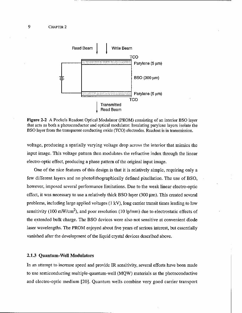
x , i
-»- z
Figure 2-6 Raman-Nath diffraction from a thin hologram showing the many diffracted orders.
which is only a few microns in thickness. First, we consider the case of a thin, elementary
sinusoidal grating which produces Raman-Nath diffraction. Standard holography is then
considered, and the effects of the various grating formation steps on hologram fidelity are
outlined.
2.3.1 Raman-Nath Diffraction
For simplicity, we first consider the diffraction from a polarization independent, sinusoidal
grating. Diffraction from such a grating forms the basis of holography, and a sinusoidal
intensity pattern is convenient for use in device simulations. Figure 2-6 diagrams the dif-
fraction from a thin slab with thickness L and a mixed type of grating formed from both
index and absorption modulation. The complex index of refraction is given by
n = n'0 +An'cosKx (2-1)
where K = 2rc/A is the magnitude of the grating vector, K, which characterizes the ori-
entation and frequency of the grating. The grating spacing, or period, is given by A, and
the refractive index components are given by
.1 (2-2)
15 CHAPTER 2
An = An + i—Aa (2-3)
For L « A, the slab essentially acts as a complex amplitude transmission filter in
which the transmission is given by [30]
T = e ° (2-4)
where
s 2TC no L
5° = IÄ (2"5)
and
8' =
L 27t_L
X. cos 9 o
-,JAn'(z)dz (2-6)
are the phase shifts, and where 0' is the incident angle inside the slab.
The readout of this grating by a plane wave with k-vector kr indicated in Fig. 2-6 pro-
duces the following field at the exit face of the slab
S« - Ereade""'T = W'V"V8'^" (2-7)
A Fourier decomposition of this field gives the far field diffraction pattern which consists
of many diffracted beams traveling in directions given by kd = kr + mK where m is the
diffraction order. This type of diffraction is known as Raman-Nath diffraction, and the
input diffraction efficiency in order m, which is the power diffracted into order m divided
by the incident power ofEread, is given by [31]
Tim = *~a°L^(|81) (2-8)
where Jm is the ml order Bessel function. Typically, only the first-order diffracted beam is
of interest and is given by
El = Bread' Tl (2-9)

Optically Addressed Spatial Light Modulators 16
where Tx is the transmission for the first-order diffracted beam. For |8'|«1, Tx is given by
T, = Ux{-h)~^ (2-10)
Thus, for small phase shifts, the first-order diffraction is linear in the phase shift and hence
linear in the index modulation.
2.3.2 Holography
Following Goodman [30], we now generalize the grating formation process to examine
standard holography with an information carrying signal beam, S, and a plane wave refer-
ence beam, R, where
R = AeikR'X (2-11)
S = a(x,y)e e {2.-11)
and a(x, y) is the real amplitude of the image to be stored in the OASLM, and <pa is the
phase. The interference of these two beams inside the OALSM produces the following
intensity pattern
/ = (A2 + a2)( 1 + -4^cos(tf x + cp«)l (2-13) V A +a J
where K = ks - kr is the grating vector. For an image with a spatial frequency bandwidth
much smaller than the magnitude of the grating vector, the intensity pattern consists of a
rapidly varying carrier with spatial frequency K/2% modulated by the slowly varying
image. In order for the OASLM to faithfully reproduce the image beam upon diffraction, it
must provide an amplitude transmission for the first order diffracted beam, Th that has an
amplitude that is linearly proportional to a(x, y) and a phase given by <pfl. During the var-
ious steps of the grating formation processes, however, there are many nonlinear effects
that can produce distortions in the transmission.

17 CHAPTER 2
Intensity Pattern
/ = (A2 + a2)(\ + -f^cosC Kx + <pa)l
Screening
Field Pattern
E = E +E'cos(Kx+q>a)
Electro-optic Effect
Complex Index Pattern
An = A«0 + An' cos ( Kx + <pa)
1st Order Raman-Nath Diffraction
Amplitude Transmission
1,(8, (pa, K, 0
Figure 2-7 The steps that produce a hologram in a MQW-OASLM. An incident intensity pattern consisting of the interference between a plane wave reference and a signal beam drives the photo- conductive screening process to produce a mimicing field pattern. Subsequent electro-optic modu- lation and diffraction lead to a first-order diffracted beam characterized by the first-order transmission. Nonlinear transport and electro-optic response as well as other effects can lead to distortions in the hologram fidelity. These distortions can arise in both the amplitude and phase of the field and index grating. The phase of the field and index gratings are denoted by <pa and <pa, respectively.
Figure 2-7 shows the sequence of grating formation steps for a photoconductive
OASLM such as the MQW-OASLM. The first step involves the creation of the screening
charge and subsequent field pattern by the photoconductive screening process. Due to car-
rier transport, this process is nonlinear, and the amplitude transmission can be distorted in
two ways: higher order Fourier components of the screening field can be created, and the
first-order field component can be distorted. Higher order gratings will diffract into higher

Optically Addressed Spatial Light Modulators 18
diffraction orders which are generally of no concern. Distortions of the first order field
component, however, lead to distortions in the image in the first diffraction order.
The next step in the hologram formation process involves the creation of the index and
absorption modulations from the field pattern. This step can also induce nonlinearities. For
example, to lowest order the electro-optic effect in quantum wells is second order in the
field; this can again lead to higher order Fourier components in the complex index pattern
as well as distort the first-order amplitude. Finally, the field amplitude that is diffracted
into the first order is, for large phase modulation, nonlinear in the index as given by
Eq. (2-10). However, for small index modulation the response is linear in the index
modulation.
The results of the above processes on the first-order transmission can be summarized
by the functional dependence of the first-order transmission on the image amplitude a, the
image phase <pa, the grating vector K, and the time t
T, = r,(a,cpfl,*:,0 (2-14)
The dependence of T, on a and cpa gives the linearity of the hologram formation pro-
cess. The K dependence of 7\ is referred to as the Modulation Transfer Function (MTF)
and characterizes the effect of the resolution performance of the OASLM on the image
transfer process. The time dependence essentially gives the exposure dependence which
may also affect the linearity. The response of some devices is linear for short exposures
but then becomes nonlinear for long exposures. We will return to these issues in detail for
the MQW-OASLM in the following chapters.
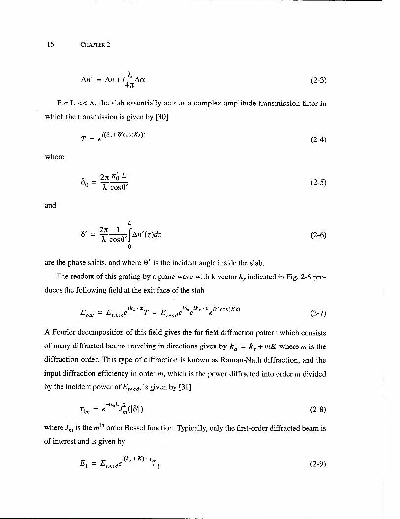
2.4 Application Example: Optical Correlator
There are many applications for dynamic OALSM's including optical processing and
display [32]. Several applications using a MQW-OASLM have been demonstrated includ-
ing a joint transform correlator [1], a short pulse auto-correlator [2], and a time-gated
19 CHAPTER 2
f(x) |p
g(x)
F(x).G(x)
f(x)*g(x). ;;.. /' j
OASLM \
Figure 2-8 A joint transform optical correlator which computes in parallel and in real time the spatial correlation between two input images. The two images are Fourier transformed onto the OASLM, producing a hologram that is proportional to the product between the Fourier transforms. A back-illuminating beam then diffracts off of this hologram, reflects off of the beam splitter, and passes through another Fourier transforming lens onto the output plane. The indicated correlation peak shows the location of the "unknown" letter 'A' in the reference image.
holographic setup for imaging through turbid media [3]. In this section, the operating prin-
ciple of a joint transform correlator is explained and used to motivate some of the more
important performance criteria of the OASLM.
Figure 2-8 shows a diagram of a joint transform correlator. The function of the correla-
tor is to compute in parallel and in real time the spatial correlation between the two input
images and present the result on the output plane. This is accomplished by taking advan-
tage of the Fourier transforming properties of lenses and of the square-law intensity
response of the OASLM.
The two images to be compared, usually an unknown image and a reference image, are
imprinted onto coherent beams using, perhaps, electrically addressed SLM's. These beams
are Fourier transformed onto the OASLM which is placed in the back focal plane of the
first lens. The hologram formed by the interference between the two beams is proportional
to the product of the Fourier transforms of the original images. This hologram can be read
out by a beam from the back which is reflected by the beam splitter and passed through

Optically Addressed Spatial Light Modulators 20
another Fourier transforming lens onto the output plane, typically a CCD detector or a
photodiode array. As indicated in Fig. 2-8, the resulting output intensity consists of a cor-
relation peak corresponding to the position of the unknown letter 'A' in the reference
image.
The overall performance of the system will in part be determined by the performance
of the OASLM. For example, the signal-to-noise ratio achieved at the detector plane is
determined by the diffraction efficiency of the OASLM. A larger diffraction efficiency
increases the intensity in the correlation peak at the detector and improves the recognition
accuracy. The number of comparisons per second will in part be determined by the frame
rate of the OASLM. The faster the grating can be formed, erased, and reset, the faster the
overall system can run. One of the advantages of using such an optical setup for this appli-
cation is that, even if the system can only run at modest speeds by electrical standards, say
100 kHz, the effective computation rate can be quite high since a whole 2D page is pro-
cessed at once. For a page with NxN pixels, the number of equivalent digital computations
goes as iV log2N, giving an equivalent computation rate of over 1 Tfiop for 1000 x 1000
page sizes running at 100 kHz [20]. For this reason alone, interest in optical correlators
has remained high since their introduction by Vander Lugt in 1964 [33].
Another very important practical consideration is the compactness of the optical setup.
In the Fourier geometry used here, the required focal lengths of the lenses are determined
by the size of the input images and by the resolution of the OASLM. With Ares denoting
the smallest spatial feature than can be resolved by the OALSM, the required focal lengths
are given by
/ = DimaSeAres (2.15)
A
where Dimage is the width of the input images and A the wavelength. Better resolution
allows a wider field of view to be imaged with smaller focal lengths.

21 CHAPTER 2
2.5 Performance Comparison
As mentioned above, frame rate, diffraction efficiency, resolution, and linearity are impor-
tant criteria to study when examining the performance of an OASLM. Other practical
considerations include applied voltage requirements, electrical power requirements, and
fabrication requirements. For example, PROM's require high voltage but little electrical
power, whereas SEED's require small applied voltages but dissipate a lot of electrical
power. Of all the devices mentioned, SEED'S require the greatest fabrication complexity
while PROM's require the least. The fabrication complexity of the MQW-OALSM is a
compromise. A summary of various performance related criteria is given in Table 2-1.
To directly compare the performance of the OALSM's mentioned above, we follow
Williams and Moddel [34, 20] and examine three criteria: bit rate per area, optical sensi-
tivity, and switching energy per bit. For non-pixellated devices, two effective bits or pixels
are assigned to the resolution limit, and the areal bit rate density gives the number of bits
in one square centimeter that can be switched in one second. This benchmark represents
an effective throughput, and allows slower devices with a large number of pixels to be
compared against fast devices with a small number of pixels. The sensitivity is simply
measured by the required optical intensity, and the switching energy per bit gives the
trade-off between speed and intensity requirements. The areal bit rate density versus sensi-
tivity is shown in Fig. 2-9 for a variety of devices along with a line of constant switching
energy at 1 pj/bit. For devices limited by photoconduction, the indicated points can slide
along such constant switching energy lines; for example, a greater bit rate can be achieved
at larger intensities. In some devices, the maximum bit rate is not limited by the photocon-
ductive response rate. For example, devices using nematic liquid crystals are limited by
the switching time of the liquid crystals, and arrays of SEED devices are limited by heat
dissipation.
As indicated in Fig. 2-9, the modified PROM structure using GaAs MQW's (1st GaAs-
OASLM) improves the areal bit rate density by three orders of magnitude. This is due to
improvements in both the frame rate and the resolution. As the "Modeled MQW-OASLM"
point shows, the optimization techniques developed in this work indicate that the

Optically Addressed Spatial Light Modulators 22
Device Resolution 50% MTF (lp/mm)
Frame Rate (Hz)
Sensitivity
(W/cm2)
Voltage (V)
Hughes LCLV
40 67 4xl0"4 10
PROM 12 lxlO4 5xl0"2 1000
OC-Si/nematic 82 50 6xl0"5 5
CC-Si/smectic 70 lxlO3 2.5xl0"4 10
SEED (20Hm) lxlO8 10 15
lstGaAs MQW-OASLM
50 3xl05 0.3 30
Modeled MQW-OASLM
140 lxlO5 lxlO"2 20
Table 2-1 Performance comparison of the optically addressed spatial light modulators discussed in this chapter. The resolution column gives, in line-pairs per millimeter, the point at which the MTF drops by 50%. For the SEED the pixel size is given. The frame rate and sensitivity give the fre- quency at which the devices can be run at the indicated optical intensity levels. The applied voltage requirements are also given. The results for the first six devices are from typical experimental op- erating conditions. The parameters for the first four devices are from [34], the SEED parameters are from [25], the 1st GaAs MQW-OASLM parameters are from [29], and the modeled MQW- OASLM parameters are from this work.
sensitivity can be improved as well, producing a device with the lowest overall switching
energy per bit. These optimization techniques are described in Chapter 7.
2.6 Summary
The search for the ideal modulator from which to produce an optically addressed spatial
light modulator involves many trade-offs, some of which are intrinsic to the materials
themselves. These trade-offs could be, for example, speed for electro-optic effect, or elec-
tro-optic effect for fabrication complexity or spectral bandwidth. For example, while

23 CHAPTER 2
E
'S3
a
CD
15
CO
10fi
106
104
S 10"
10°
~i 1 1 1 r
N»SEED
10z
V • Modeled MQW-OASLM 1slGaAs xv MQW-OASLM V
°'t N • a-Si/FLC
PROM • v v ^ • a-Si/nematic
Hughes LCLV • ^ x
10° 10"2
Intensity (W/cm2)
10" lO"6
Figure 2-9 Comparison of the bit rate per area and intensity requirements for the OASLM's dis- cussed in this chapter. The lpJ/bit switching energy per bit line gives the trade-off between bit rate and intensity for photoconductive-limited devices. The modeling of the MQW-OASLM perfor- mance in this work indicates that this device can have the lowest switching energy per bit of all the illustrated devices.
nematic liquid crystals display large electro-optic effects, they are intrinsically slow due to
the physical effect of having to rotate an entire molecule during the modulation process.
Ferroelectric liquid crystals overcome this limitation, but at the expense of only being able
to produce a binary response. Other limitations occur in electro-optic materials used in
PROM type geometries which rely on the carrier transport and linear electro-optic mate-
rial properties. Is these materials, these two processes are linked via the lattice
polarizability [35]. Thus, for example, materials with good lattice polarizability such as
Lithium Niobate (LiNb03) tend to have large electro-optic effects but poor carrier trans-
port behavior due to large phonon scattering. On the other hand, materials such as GaAs
with low lattice polarizability have very good transport behavior but weak linear electro-
optic effects. The MQW-OASLM overcomes this limitation in the PROM geometry by
decoupling the source of the transport behavior from the source of the electro-optic effect.
The trade-off here is in increased fabrication complexity, and a quadratic and wavelength-
resonant electro-optic response. Compared to other devices such as the SEED, however,

Optically Addressed Spatial Light Modulators 24
the MQW-OASLM fabrication is much simpler, and overall it provides a nice compromise
among the various trade-offs, producing a device with very good resolution, bit rate, and,
as we shall see in Chapter 6, linearity.

Chapter 3
Optical and Transport Properties of Multiple-Quantum-Wells
As discussed in the previous chapter, the success of the MQW-OASLM depends on the
combination of the fast carrier transport and the sensitive electro-optic properties of quan-
tum wells. This combination arises from quantum confinement which creates a very large,
resonant electro-optic effect while retaining the good carrier mobilities of gallium ars-
enide. This electro-optic effect, known as the quantum confined Stark effect, is more than
three orders of magnitude stronger than the intrinsic Pockels effect in GaAs. While the
carrier mobilities remain high in MQW structures, carrier transport is not completely unaf-
fected by quantum confinement. Two types of carriers with very different transport charac-
teristics are created: confined carriers in the well subbands, and free carriers in the
transport bands above the barriers. One of the main challenges in modeling such a system
is finding a way to include quantum wells in standard semiconductor device models so
that practical simulation-related issues such as boundary conditions and multiple time
scales can be realistically addressed.
This chapter begins with a brief review of the electronic structure of bulk gallium ars-
enide, followed by a discussion of the confined states in a GaAs/AlGaAs quantum well. A
summary of the main optical properties of GaAs/AlGaAs quantum wells is presented,
including a discussion of excitonic absorption, the quantum confined Stark effect, and the
use of quantum wells as the source of a very large, resonant electro-optic effect. The
25

Optical and Transport Properties of Multiple-Quantum-Wells 26
impact of quantum confinement on carrier transport, including a detailed calculation of the
escape rates of confined carriers, is then presented. Finally, a shallow trap model which
allows the inclusion of quantum wells in the standard semiconductor drift-diffusion model
is described.
3.1 Electronic Structure
Gallium arsenide (GaAs) is a very versatile and high performance semiconductor that is
used in a variety of opto-electronic applications such as photo-detectors, light emitting
diodes, and diode lasers. Its material and electronic properties have been studied and opti-
mized over the last several decades, and, along with aluminum-gallium-arsenide
(AlGaAs), it is one of the most reliable and popular materials used in fabricating quantum-
well devices. As this materials system is the basis for the devices studied in this thesis, we
shall use it as an example throughout this chapter.
GaAs is a III-V compound semiconductor that crystallizes into a zinc-blende type unit
cell. As in all crystalline solids, the periodic potential induced by the repeating unit cells
produces a one-electron Hamiltonian with translational symmetry along the lattice. The
corresponding electron eigenstates are known as Bloch functions and consist of the prod-
uct of a periodic function, unk, with the same periodicity of the lattice and a more slowly
varying plane wave envelope function [36]. These eigenstates are written in the form
(r\nk) = ynk(r) = eikrunk(r) (3-1)
The space coordinate is given by r. The eigenstates are characterized by the band index, n,
and the Bloch wavevector, k. Figure 3-1 shows a plot of the band diagram for GaAs along
various lines in &-space. Each curve, or band, corresponds to a different value of n. The
band energies are plotted between special symmetry points of the zinc-blende Brillouin
zone. The room temperature GaAs bandgap of 1.42 eV occurs at T(k=0) in the Brillouin
zone, separating the lower and upper bands into valence and conduction bands, respec-
tively. Optical and thermal excitation of electrons from the valence to conduction bands

27 CHAPTER 3
>
D) 1—
CD C
111
Wavevector k
Figure 3-1 Band diagram of bulk GaAs showing the direct bandgap and degenerate hole bands at T. Other conduction band minima, or valleys, at L and X play important roles in carrier transport and carrier escape from quantum wells. After Kittel [37].
produces vacancies in the valence bands known as holes. An important feature of the
bands near k=0 is that they are approximately parabolic in k (k = |A;|). This is similar to
the case of a free electron in which the free space kinetic energy is quadratic in k. Also, as
in the free space case, the curvature of the energy vs. k curve can be related to an effective
mass of the particle. For example, in the case of GaAs, the two degenerate hole bands at T
are denoted the light hole (LH) and heavy hole (HH) bands due to their different effective
masses.
The conduction band in GaAs displays parabolic local minima, or valleys, at other
points in fc-space, namely near h=n/a( 1,1,1) and X=27t/a(0,0,l) where a is the lattice con-
stant. These valleys can become occupied through high energy phonon scattering and can
greatly affect the carrier transport properties, as well as the escape rates, of carriers in
quantum wells. These issues will be discussed below.
Alloys of GaAs such as A^Ga^As can be formed through suitable fabrication tech-
niques, although they are not truly crystalline but rather a type of solid solution. However,
for most basic electronic calculations it has been found that treating the potential as a
weighted average over the crystalline potentials of GaAs and AlAs produces acceptable
results and allows the retention of the Bloch formalism [36]. The bandgap of Al/ja^As

Optical and Transport Properties of Multiple-Quantum-Wells 28
GaAs -\ ^-— Alo.3Ga0.7As X
substrate
i—i
100 Ä
n^^j"
— z
Figure 3-2 Sketch of a GaAs/AlGaAs multiple-quantum-well structure which is typically grown on top of a GaAs substrate wafer. The growth direction is along z, and the corresponding variations of the conduction and valence band edges are shown.
varies linearly with composition from the bandgap of GaAs up to that of Al 4Ga6As (from
1.42eV to 1.92eV) with only a minimal change in lattice constant. This allows the fabrica-
tion of high quality heterostructures made of layers of differing compositions. These
multi-layer heterostructures are typically fabricated using either molecular beam epitaxy
(MBE) or metal organic chemical vapor deposition (MOCVD). In MBE, the layers are
grown one atomic layer at a time in ultra high vacuum conditions from the evaporation of
solid sources [38]. In MOCVD, the reaction of gaseous group III alkyls and group V
hydrides over a heated substrate is used to grow epitaxial layers [39]. Abrupt composi-
tional transitions of a monolayer can be routinely made with these techniques.
A GaAs/AlGaAs multiple-quantum-well structure consists of thin (-100 Ä) alternat-
ing layers of GaAs and A^Ga^As. A diagram of the band edges in a typical
GaAs/AlGaAs MQW structure is shown in Fig. 3-2. The alternating energy along z breaks
the translational symmetry of the bulk material, and the larger bandgap AlxGa1.xAs 'barri-
ers' confine the lowest lying electron and hole states to the smaller bandgap GaAs 'well'
regions. To describe this confinement, the plane wave envelope function in the bulk Bloch
function, Eq. (3-1), must be replaced with an envelope function of the form
X(z)e ikx ■ r±
(3-2)

29 CHAPTER 3
r h2
E1
I HH-i LHj --
LH2 - - HHc
Figure 3-3 Electron(E), heavy hole(HH), and light hole(LH) subbands for an isolated GaAs/Al0 29Gag 71 As quantum well with a well width of 100 Ä. The bandgap between the con- duction and valence band has been shrunk to highlight the well states. Note the smaller barrier height for the hole states and the large number of subbands for the heavy hole due to its larger ef- fective mass.
where % is a confined envelope wavefunction and k± and r± are the components in the x-y
plane [36]. The states are thus confined along the growth direction, z, but are free in the x-
y plane.
Near k± = 0, % solves the envelope Hamiltonian of the form
r a 1 a % + V(z)% = E% (3-3)
2 dzm(z)dz
where m(z) is the effective mass in the different layers, V(z) is the band edge potential
energy, and E is the energy eigenvalue [36]. Equation (3-3) is solved along with continu- 1 a
ous boundary conditions on % and — ^-% at the interface between different layers.
The bulk properties of the different layers are encapsulated into the effective electron
and hole masses and the confining barrier potential. Equation (3-3) is essentially the prob-
lem of a particle in a box. Each bulk band, conduction or valence, produces a correspond-
ing set of solutions to the above Hamiltonian called subbands. For GaAs, the most
important subbands are the light and heavy hole subbands in the valence band and the
electron subbands in the conduction band. As an example, the energy levels for these sub-
bands are indicated in Fig. 3-3 for an isolated quantum well with the following properties:

Optical and Transport Properties of Multiple-Quantum-Wells 30
well width = 100 A, x = 0.29, and barrier height and effective masses from Moss [40]. In
this example, there are two electron subbands, five heavy hole subbands, and two light
hole subbands. While the hole energies are degenerate in bulk GaAs, in quantum-well
structures this degeneracy is removed in the subbands because of the different hole effec-
tive masses.
While the vertical motion of the electrons is confined, the in-plane behavior resembles
a 2D electron gas in which the electron momentum is given by fikj^. The above analysis
has been for k± = 0 which, for most of our work, is sufficient for the calculation of %. For
k± * 0, mixing can occur between the different subbands, distorting them from a nominal
parabolic shape. For our purposes, however, it will be adequate to approximate subbands
as parabolic with appropriate effective masses.
3.2 Optical Properties
The quantum confinement of electrons and holes produces very noticeable effects on the
optical properties of quantum-well structures. At special exciton resonances, the absorp-
tion increases dramatically, and both the absorption and index of refraction become very
sensitive to an applied electric field. From a device perspective, this allows the construc-
tion of very low voltage, compact optical modulators.
3.2.1 Excitons
The most obvious optical property affected by quantum confinement is the absorption
spectrum. Fig. 3-4 shows the absorption spectrum at zero applied voltage for the 100 Ä-
GaAs/35 Ä-Al0 29Ga0 71 As MQW system in the active region of the MQW-OASLM
described in Fig. 2-5. This data was taken with a 0.5 m monochromator illuminated with a
white light source and with an output FWHM resolution of 1 nm. An AC applied voltage
was used to suppress the screening effects described in Chapter 4. Just past the absorption
edge at -850 nm, two prominent peaks are evident. These arise from a many body state
called an exciton that is due to the correlated interaction of electrons in the quantum

31 CHAPTER 3
2 104 i I i i i i
-OV -4V -8V -12V
830 835 840 845 850 855 860 865 870 Wavelength (nm)
Figure 3-4 Absorption spectrum of a 155 period 100 Ä-GaAs/ 35 Ä-Al0 29Ga0 71As multiple- quantum-well system for the indicated applied voltages. The corresponding fields are 0,11.8,23.6, and 35.4 kV/cm. The two peaks are caused by exciton absorption, and the red shift and decay of the peaks as the field is increased are due to the quantum confined Stark effect.
wells [13]. During absorption of a photon, an electron is promoted from one of the valence
subbands to one of the conduction subbands. The resulting vacancy, or hole, and the elec-
tron form a bound electron-hole pair which, formally, resembles a 2D hydrogenic state
characterized by an effective Bohr radius XQ [36]. The quantum confinement provided by
the barriers produces a tightly bound exciton state and thereby stabilizes the exciton
against field and phonon ionization. The exciton binding energy arises, essentially, from a
reduction in the electron-electron repulsion in the interacting, many body system. The
strongest exciton resonances correspond to the most tightly bound exciton states.
Each valence-conduction subband combination offers the possibility of forming an
exciton resonance, though the absorption coefficient of many combinations is suppressed
due to polarization and parity considerations [36]. In Fig. 3-4, the peak at 840 nm corre-
sponds to the exciton created between the LHj and Et subbands, and the peak at 847 nm
arises from the HHj and E! subbands.

Optical and Transport Properties of Multiple-Quantum-Wells 32
Not only does quantum confinement stabilize the exciton, but the enhanced overlap
between the electron and hole states produces a larger absorption coefficient. The peak
absorption due to the most tightly bound exciton state (IS) can be estimated as [36]
471 e EP I, (A), («)v|2 1 a = ^l<X IX >l —7= (3-4)
where Ep is the product of the electron effective mass and the square of the velocity matrix
element between valence and conduction band atomic basis functions, n is the index of
refraction, c is the speed of light, m0 is the electron effective mass, L is the device length,
co is the optical frequency, %^ and yf& are the hole and electron envelope wavefunctions,
respectively, and T is the width of the exciton resonance curve which is typically a
Gaussian. The exciton absorption from Eq. (3-4) is typically over an order of magnitude
larger than the non-resonant, continuum absorption that occurs at shorter
wavelengths [36]. Note the strong dependence on the overlap between the electron and
hole envelope wavefunctions.
3.2.2 Quantum Confined Stark Effect
The application of a uniform electric field along the growth direction in a MQW structure
drastically alters the absorption spectrum. This is illustrated in Fig. 3-4 for applied volt-
ages from 0 to 12 V, which corresponds to applied fields from 0 to 35 kV/cm. Two obvious
trends are evident: a red shift of the resonant wavelength of the excitons to longer wave-
lengths as the field is increased, and a corresponding reduction in the maximum value of
the absorption peaks. The origin of these effects lies in the changes induced by the applied
field on the electron and hole envelope wavefunctions. Sketches of the effective potential
(band edges) and the resulting envelope wavefunctions are shown in Fig. 3-5 for a
GaAs/AlGaAs quantum well in zero applied field and in an applied field of 100 kV/cm. At
large fields, the ramping potential polarizes the electron and hole states at opposite corners
of the well, reducing the wavefunction overlap. From Eq. (3-4), this reduces the peak
value of the absorption. As the wavefunctions polarize at opposite sides of the well, they

33 CHAPTER 3
Field=0 "^P-
3
Q. E < c o
1
0.8
0.6
0.4
0.2
i ' ■ ■ ■ i ■ ■ ■ ■ i ■ ■ ■ ■ i ■ ' ' ' i
Heavy hole
Electron
-150 -100 -50 0 50 100 150 z(A)
Field=100kV/cm -}#^
^
•o
Q. E < c g c
"35
1
0.8
0.6
0.4
0.2
Heavy hole
Electron
-150 -100 -50 0 50 100 150 z(A)
Figure 3-5 Illustration of the changes in the electron and heavy hole wavefunctions due to the quantum confined Stark effect as computed using the transfer matrix method for a single 100 Ä- GaAs/Al0 29Gao.7iAs quantum well. For zero applied field, as shown on the left, the electron and heavy hole wavefunctions are centered in the well which is indicated by the two vertical lines. For non-zero field, the electrons and holes become polarized at opposite sides of the well.
also "sink" into their respective corners of the well causing a reduction, or red shift, in the
resonant energy. This field dependent effect is known as the quantum confined Stark effect
(QCSE) and is, to lowest order, quadratic in the applied field [13].
The calculation of the envelope wavefunctions in an applied field requires the solution
of the envelope Hamiltonian, Eq. (3-3), with the band edge potential including the linear
ramp from the applied field. Approximate results can be obtained with variational
treatments [41], but since the carriers can tunnel out of the well on the downstream side
the states are actually quasi-bound and are more accurately handled with numerical tech-
niques. One of the most convenient techniques for handling this situation is the transfer
matrix technique (TMT) [42, 43]. This technique involves discretizing the band edge
potential into small regions of uniform energy which can then be solved with plane wave
solutions. Matching boundary conditions across regions allows for a scattering type of
treatment in which the occupation probability inside the well is calculated over a range of
energies. The peak in this probability vs. energy curve gives the quasi-bound energy, and

Optical and Transport Properties of Multiple-Quantum-Wells 34
(a)
4000
2000
-T o E
< -2000
-4000
-6000
."' '■■'■<■■■*/• i i i i | i i i i | \
......... \ .
• r \ • t \
-
•
" ■! _ •» • * i i —4v :
i ; i '
8V • -.—12V-
830 835 840 845 850 855 860 865 870 Wavelength (nm)
(b) c <
0.02
0.01
0
-0.01
-0.02
-0.03
-0.04 E-
-0.05 830 835 840 845 850 855 860 865 870
Wavelength (nm)
Figure 3-6 a) Absorption change induced by the QCSE. b) Corresponding index change calculat- ed via a Kramers-Kronig transformation of a).
the width of the curve gives the tunneling lifetime of the quasi-bound state [43]. The
results in Fig. 3-5 were computed using this technique.
: -T .........
• /\
•_,.;. 1_ •
/ i
-.-.>-.
• V.'?
; i \ * h i i -
i1- —4v ; 1 1 i i 8V :
- — -12V -
\ .... i. ■ i i i i i i ,
3.2.3 Electro-optic Effect
The large changes in absorption due to the QCSE (greater than 6000 cm"1 at 50 kV/cm)
can be exploited to produce a sensitive electro-optic effect that replaces the rather weak
linear electro-optic effect in GaAs (An - 10"6 at 50 kV/cm). The wavelength dependence
of the absorption change for various voltages, i.e. a(V) - a(0), is shown in Fig. 3-6a. Since

35 CHAPTER 3
there are large wavelength dependent changes in the absorption, there are also large
changes in the index of refraction. The result of a Kramers-Kronig transformation on the
absorption-change spectrum produces the corresponding index-change spectrum shown in
Fig. 3-6b. Index changes as large as 0.05 at 50 kV/cm are produced by the QCSE.
When using the QCSE induced absorption and index modulation as an electro-optic
effect, it is important to note two things. First, it is a resonant effect, producing large mod-
ulation only for wavelengths near the exciton resonances. The spectral bandwidth is only
about 5 nm. Second, to lowest order, the changes are quadratic in the internal field for
symmetric wells. This limits the response at low applied fields.
3.3 Transport Properties
Besides giving rise to the quantum confined Stark effect, the quantum confinement of car-
riers also significantly alters the carrier transport properties of quantum-well devices.
Essentially two types of carriers are created: well-confined carriers that only transport in
the plane of the wells, and free-carriers which undergo bulk-like transport above the barri-
ers. Carrier exchange between these two types of carriers occurs through various escape
and capture events. In this section, a shallow trap model is described which allows these
two types of carriers to be straightforwardly included in standard semiconductor transport
models. A detailed calculation of the escape rates for both electrons and holes is also pre-
sented.
3.3.1 Vertical vs. In-plane
The carrier transport in a MQW structure is highly anisotropic since the carriers in the
wells are confined in the growth, or so-called vertical, direction but free in the transverse,
or in-plane directions (see Fig. 3-7). Well-confined carriers can also escape into the trans-
port bands above the barriers where they undergo transport in both the vertical and trans-
verse directions. The carrier transport in most devices is usually dominated by only one of
these types of transport. For example, the transport in optical modulators and p-i-n

Optical and Transport Properties of Multiple-Quantum-Wells 36
Figure 3-7 A plot of the conduction band energy for a quantum-well system over two spatial di- mensions. Carriers in the wells are confined along the growth (z) direction but are free to transport in the plane of the wells (x). Carriers in transport bands above the barriers can transport in both di- rections. The two types of carriers are connected via escape and capture processes.
photodiodes is exclusively along the vertical direction while the transport in modulation
doped field effect transistors is along the in-plane direction. In contrast, in the MQW-
OASLM we must consider both types of transport.
The in-plane transport of carriers in a quantum-well can be modeled in a fashion simi-
lar to bulk transport by using a drift-diffusion model. The drift-diffusion model considers
the change in the carrier concentrations caused by the differential flux of drift and diffu-
sion currents. It can be derived from the first moment of the Boltzmann transport equation
and is the standard model for simulating transport in semiconductors [44]. For example,
this model has been used to simulate in-plane transport in modulation-doped field effect
transistors [45] and photorefractive quantum-well devices [46].
Vertical transport involves the escape of carriers from the wells, transport in bulk-like
states above the barriers, and then recapture back into the wells. For typical capture times
and transit times, a carrier undergoes many of these escape/transport/capture cycles during
transit across the MQW region. As we show below, this process can also be modeled using
a drift-diffusion model for transport above the barriers, and appropriate escape and capture
rates describing the exchange between well-confined and free carriers.

37 CHAPTER 3
- Thermionic
Tunneling from subband 2
Tunneling from subband 1
Figure 3-8 The escape of electrons from a quantum well via thermionic emission and tunneling. In the Moss model, carriers with a 3D density of states in the tail of the indicated Boltzmann distri- bution escape via thermionic emission. Carriers with a 2D density of states in each of the well sub- bands escape via tunneling through the downstream barrier. The tunneling time for carriers in the second subband is very short due to the smaller barrier height.
3.3.2 Escape Mechanisms
There are many processes by which a carrier confined in a quantum well can escape into
the continuum above the barriers or into a neighboring well. Inter-well processes include
miniband conduction in Bloch-like states created from the quantum-well superlattice [47],
phonon scattering transitions between subbands in neighboring wells [48], and direct, res-
onant tunneling between neighboring subbands [49]. Continuum-escape processes include
thermionic emission and coherent tunneling across neighboring wells [50]. The signifi-
cance of each process depends strongly on the barrier height, barrier thickness, and tem-
perature.
At room temperature, and for barrier thicknesses greater than 20 Ä, thermionic emis-
sion and coherent tunneling are expected to be the dominant escape processes [50]. Ther-
mionic emission is the escape of carriers in the tail of the Boltzmann distribution with
energies above the barrier height. Tunneling is the escape of carriers via coherent, quan-
tum mechanical tunneling through a finite barrier. These two processes are in fact linked
since the thermal occupation of higher subbands allows for faster escape by tunneling
through a smaller barrier height as diagrammed in Fig. 3-8. Several theories which treat
these processes separately have been presented in the literature [51, 52]. However, a more

Optical and Transport Properties of Multiple-Quantum-Wells 38
complete model which considers these two processes together has recently been presented
by Moss et al. [40]. We now briefly outline this model and give some results for a
GaAs/AlGaAs quantum-well system.
In the Moss model, the carriers in one quantum-well period are assumed to be of two
types: 2D, confined carriers with energies below the top of the barrier, and 3D, bulk-like
carriers with energies above the barrier. The escape of carriers out of the well region is
described by
f ■ "f where N is the effective total volumetric density of carriers in one quantum-well period
and x is the escape time given by
\ •?-+?£ <3-6> where l/iTE is the escape rate due to the thermionic emission of the 3D carriers with
energies above the barrier, and fi/ii is the escape rate of the 2D carriers in the ith sub-
band due to tunneling through the downstream barrier into the continuum. The fractional
occupancy of the i subband in thermal equilibrium is given by/), and x,- is the corre-
sponding tunneling time. The/j's are calculated by counting the fractional occupancy of
each subband, taking into account the 2D density of states for well-confined carriers and
the 3D density of states for unconfined carriers. One subtlety of this calculation is the con-
version of the surface density of confined carriers to an effective 3D volumetric density by
dividing the surface density by the quantum-well period. The subband tunneling times are
calculated using the TMT technique described previously. For the thermionic emission of
electrons, Moss considers the escape from both the T and L valleys in the wells into the T
valley in the barriers. The contribution of L-valley electrons can be significant for large
barrier heights.
The thermionic emission rate follows an Arrenhius type of behavior:

39 CHAPTER 3
1 „-AEh/kRT XTE
~ e b' "-B1 (3-7)
where kBT is the thermal energy and AEb = Vb - eFd/2 is the downstream barrier
height that is decreased from the zero field barrier height of Vb by the applied field, F, over
the quantum-well width d. The thermionic emission rate thus increases slightly with
applied field and is very sensitive to the barrier height Vb.
The tunneling rate of a given subband depends on the thermal occupation of the sub-
band and on the subband lifetime. The occupancy of a subband in thermal equilibrium
shows an Arrenhius type dependence on the subband energy, Eb
f. _ e-Ei/k"T (3_8)
and thus decreases significantly for higher subbands. The lifetime also depends strongly
on the subband energy. It can be estimated from the Fowler-Nordheim tunneling equation
for a particle with mass m and subband energy Ei as [53]
%t~e 3 eFh (3-9)
and decreases strongly for higher subbands. Thus, even though higher subbands may not
be significantly populated, at large fields their carrier lifetimes may be short enough to
allow them to dominate the escape process.
Using the above model, we now present some calculations of the escape rate for the
MQW system used in the MQW-OASLM described in Chapter 2. This system consists of
100 A-GaAs / 35 Ä-Al0 29Ga0 71As quantum wells. The subband energies in Fig. 3-3 are
for an isolated well of this system. We first present the electron results. The escape rate is
calculated by computing the subband energies and lifetimes using the TMT method. We
consider a two well system and calculate for the upstream well. This gives some indication
of the effect of downstream wells in a mM/ri-quantum-well system. As discussed above,
there are two subbands in each well. The resulting escape rate versus applied field is
shown in Fig. 3-9. For small fields, thermionic emission dominates the escape process

Optical and Transport Properties of Multiple-Quantum-Wells 40
0 20 40 60 80 100 Field (kV/cm)
Figure 3-9 Escape rates for electrons and holes computed using the Moss model. The low-field rates are determined by thermionic emission, with the holes demonstrating an order of magnitude faster rate than the electrons due to the much smaller barrier height in the valence band. Tunneling becomes significant at large fields, especially for electrons.
while at larger fields the tunneling of electrons from the thermally occupied second sub-
band dominates.
Similar calculations can be performed for holes. In this case the light holes and heavy
holes each produce different thermionic emission and tunneling rates, although only T val-
ley emission needs to be considered. As discussed above, there are five heavy hole sub-
bands and two light hole subbands. The net escape rate for both types of holes is also
shown in Fig. 3-9. At low fields, thermionic emission dominates the escape as was the
case for electrons. The escape rate for holes, however, is much faster than the escape rate
for electrons since the valence band barrier height is smaller. As the field increases, the
escape rate increases first due to tunneling from the second light hole subband, and then
increases again due to tunneling from the first light hole subband. Due to their large effec-
tive mass, heavy holes do not tunnel well.
As we shall see in following chapters, fast escape rates are very important to overall
device performance. Generally, obtaining fast escape rates requires the use of 'shallow'
quantum-well systems in which the barrier heights are very small. Short barriers, however,

41 CHAPTER 3
weaken the quantum confinement. This can lead to fast exciton ionization and a weaken-
ing of the exciton absorption and QCSE. Good electro-optic response, however, has been
demonstrated in an Al0 ^GaQ 9As/Al016GaQ 84As system with a very small electron barrier
height of only 50 meV [54]. Repeating the above calculations for such a system gives
escape rates for both electrons and holes greater than l.OxlO12 s"1, even at low fields.
3.3.3 Shallow Trap Model
The treatment of the escape of carriers out of the wells described above along with free-
carrier capture processes is reminiscent of the Shockley-Read-Hall model for traps in bulk
material [55]. In fact, this analogy has been used to include quantum wells in above-bar-
rier transport models in a relatively simple way [56, 57]. In particular, Magherefteh et al
have developed a conventional drift-diffusion model in which the wells are treated as shal-
low traps [28]. In this model, the discrete wells are replaced by the effective 3D volumet-
ric density of carriers in each quantum-well region. The carriers in the well regions are
coupled to the continuum, or free carriers, by the escape processes described above. As
shown in Fig. 3-10, free carriers can also be captured by a well, i.e. a shallow trap, by
phonon-scattering or other mechanisms [58]. These capture processes are characterized by
capture times %n and xp for electrons and holes, respectively. Experiments have shown
these capture times to be very fast, less than 1 ps [59]. The treatment of quantum wells as
shallow traps is sketched in Fig. 3-10. The quantum-well escape and capture processes are
treated as emission and capture processes from shallow traps within a bulk material. The
relevant escape (emission) rates and capture times are described in the figure caption.
Quantum-well structures also contain intrinsic or intentionally doped midgap impurity
or defect sites that can also act as traps. The trapping of carriers by these sites is modeled
using the Shockley-Read-Hall recombination model which uses a similar capture/emis-
sion picture of trapping [55]. While free-carrier to midgap trap transitions could be con-
sidered in this quantum-well shallow trap model, only well to midgap trap transitions are
included since the capture of free carriers by the wells is so fast. In Fig. 3-10, the capture
of well-carriers by the midgap trap is characterized by the lifetimes xN and %P for electrons

Optical and Transport Properties of Multiple-Quantum-Wells 42
•n>C -
Figure 3-10 Diagram on the left shows escape and capture processes into and out of the quantum wells and trapping into the midgap traps. The diagram on the right shows the shallow trap model of MQW's in which the quantum wells are treated as shallow traps within a bulk material. The indi- cated escape, capture, and midgap trap rates are: ß^pwell-electron escape rate, tn=free-electron capture time into the wells, and iN=well-electron lifetime for trapping into midgap traps. Hole pa- rameters are similar.
and holes, respectively. For the operating regimes we consider, we neglect the thermal
emission from the midgap traps.
In an extension of this basic shallow trap model, we also include the transport of carri-
ers in the plane of the wells by adding a conventional drift-diffusion term to the continuity
equations. Denoting the above-barrier, free-carrier densities as n and p, and the well-con-
fined or shallow trap carrier densities as N and P, for electrons and holes, respectively, the
well-carrier continuity equations are
dt e öx xn VN xN'
(3-10)
dP dt e dx +*-(h+±
where the capture and emission parameters are described in Fig. 3-10 and where
JN = e^N[NEx+VT-£j
(3-11)
(3-12)

43 CHAPTER 3
jP = ev,P[pEx-VTd£) (3-13)
are the drift-diffusion current densities in the plane of the wells. The mobilities for elec-
trons and holes are given by \iN and \ip, respectively, VT=kBT/e is the thermal voltage, with
kBT the thermal energy, and e the electron charge. The transverse field is given by Ex.
These equations will be used in conjunction with continuity equations for free-carrier
transport and other equations to construct a full model of device operation in the following
chapters.
3.4 Summary
One of the primary motivations for using quantum wells as the optical modulator in opti-
cally addressed spatial light modulators is the very strong electro-optic effect produced by
the quantum confined Stark effect. This effect is a direct result of the quantum confine-
ment of electronic states and produces index and absorption changes much larger than
those which can be obtained in bulk material. The operation of OASLM's such as the
MQW-OASLM, however, rely not only on the optical properties of the medium, but on the
carrier transport properties as well. Quantum confinement essentially produces two classes
of carriers: well-confined carriers that transport in the plane of the wells, and free-carriers
that show bulk-like transport above the barriers. To handle these two classes of carriers, a
shallow trap model for quantum wells was presented that allows the quantum wells to be
included in the standard semiconductor drift-diffusion transport model in a familiar way.
As we shall see in subsequent chapters, one of the most important performance related
features of this model is the escape of carriers from the wells into the above-barrier bands.
A detailed analysis of this process was given using a model that considered both thermi-
onic emission and quantum mechanical tunneling. It was found that attaining fast escape
rates at all field values requires the use of shallow quantum wells with very fast thermionic
emission rates.

Chapter 4
Electric Field Screening
Device operation in multiple-quantum-well optically addressed spatial light modulators
(MQW-OASLM) occurs through the screening of an applied voltage via the transport and
trapping of photocarriers. While the most interesting and useful applications involve
image formation, it is first necessary to treat the more basic case of uniform illumination
in order to understand the screening process. This allows a more direct analysis of many
important elements of device operation, such as the distributions of the interior carrier
densities and the different types of operating regimes. As a case in point, the often used
explanation of device operation describes screening as occurring through the accumula-
tion of surface charges, yet no detailed model has been given to support this picture [29].
The only model presented to date to describe screening has been an equivalent circuit
model by Nolte [15] which, as we show below, implicitly assumes dielectric relaxation.
There has also been no previous attempt to explicitly include quantum wells in a device
model. As we also show, quantum wells play an important role in determining the overall
speed response.
In the basic MQW-OASLM design [6, 29, 61], a semi-insulating MQW region is
sandwiched between two insulating buffer layers and two transparent electrodes as shown
in Fig. 4-1. As discussed in Chapter 2, device operation occurs through the transport and
trapping of photogenerated charge. Photogenerated carriers are separated by the applied
field and drift toward the semiconductor-insulator interfaces where they are stopped by
44

45 CHAPTER 4
the large bandgap insulating layers and accumulate in traps near the interfaces. A spatially
varying image input to the device produces a corresponding spatially varying surface
charge at the semiconductor-insulator interfaces. This surface charge screens the applied
voltage and creates an electric field pattern that mimics the input image. The field pattern
then modulates the quantum confined Stark effect (QCSE) to produce an index and
absorption pattern. The transport of carriers along the bias field and along the transverse
direction determines the speed and resolution performance.
In this chapter, we develop a ID drift-diffusion model of screening that is appropriate
for uniform illumination conditions. The shallow trap model from Chapter 3 is used to
describe the carrier occupation of the quantum wells. The carrier distributions are explic-
itly calculated in the quasi-steady state regime, and an injection model is developed to
model screening using simplified numerical solutions. Full numerical solutions of the
transport equations are then used to verify the main results of the injection model and to
examine the effects of drift velocity saturation. Other properties specific to quantum wells,
such as resonant absorption and field dependent carrier emission, are examined with
regard to speed performance.
4.1 Device Model
In the original MQW-OASLM design, the MQW region was made semi-insulating
through proton implantation or Cr-doping, and the buffer layers were fabricated from insu-
lating phosphate-silica-glass [6, 29]. Subsequent modifications have included substituting
semi-insulating material in place of the insulators [60], using only one buffer layer [61],
and using intrinsic rather than semi-insulating quantum-well material [62]. In this chapter,
we consider a symmetric device structure, as shown in Fig. 4-1, with an interior MQW
region of length 2L surrounded by large bandgap, insulating layers each of thickness d.
Semi-insulating or intrinsic MQW material is modeled using deep, donor-like traps with
density ND, partially compensate by shallow acceptors with density NA. Throughout most
of the interior, the uniform density of donors is denoted N'D, while in a thin region of

Electric Field Screening 46
(a)
w=
(b) .X
-y >
e2 £1 £2
-*- z
-L-d -L I I
L L+d 1 I
Figure 4-1 a) Band diagram used in device model showing interior quantum-well region sur- rounded by large bandgap insulating layers. Capture and emission processes for free and well car- riers and the trapping of well-carriers in midgap donor-like traps are also shown, b) Device geometry showing interior quantum-well region of thickness 2L with dielectric permittivity £j and insulating regions of thickness d with dielectric permittivity e2. The thin regions of width ws con- tain increased trap densities to hold the screening charge, oA and aB, at the semiconductor- insulator interfaces. Light is incident from the left and only ID transport along z is considered.
thickness ws near each of the semiconductor-insulating interfaces, the trap density is
increased to iV^. These thin (ws ~ 50 nm), high density trap regions are used to model sur-
face traps and devices in which ion implantation or low temperature growth has been used
to increase the trap density near the semiconductor-insulator interfaces in an attempt to
improve resolution performance [29, 61, 63]. While the diagram in Fig. 4-lb shows a two-
dimensional device geometry, for uniform illumination conditions only a one-dimensional
device model along the quantum-well growth direction is necessary.
To model the screening process, we consider free electron and hole transport along
with carrier transport in the quantum wells. The carriers confined in the wells are modeled

47 CHAPTER 4
using the shallow trap model developed in Chapter 3. The densities of free carriers above
the barriers, denoted by n and p for electrons and holes, respectively, are treated using a
conventional drift-diffusion model in which the wells act as shallow traps. The carriers
confined in the wells, with effective volumetric densities denoted by iV and P, escape
through thermionic emission and tunneling or become trapped in the midgap donor-like
traps. Thermal excitation from the donor-like traps is neglected, and, for most of this chap-
ter, non-resonant optical generation across the barrier bandgap is considered. The effects
of resonant absorption between well subbands and QCSE absorption are briefly discussed
in section 4.6. The rate equations for the densities of well carriers and the midgap donor-
like traps are
l = x7(Pw+Y^)iV (4_1)
I7 = f-(ß/> + Y/>(Ak-A£))P (4-2)
-^ = yP(ND-N^)P-yNN^N (4-3)
where the capture times of free carriers into the wells are given by xn and xp for electrons
and holes, respectively, and the emission rates of confined carriers out of the wells are ß^
and ßp for electrons and holes, respectively. As discussed in Chapter 3, the emission rates
are field dependent due to the lowering of the barrier heights in large fields. The recombi-
nation coefficients for the trapping of well carriers into the donor-like traps for electrons
and holes are yN and jp, respectively, and the density of unoccupied donor-like traps is
given by ND. It should be noted that the donor-like trap recombination in Eqs. (4-1) and
(4-2) is written directly in terms of the trap density rather than as a constant lifetime as
was done in Chapter 3. In principle, this allows for an investigation of trap saturation,
although for the regimes we consider this is not really an issue.
The continuity equations for free carriers are taken from standard semiconductor
transport models [44, 64] and are given by
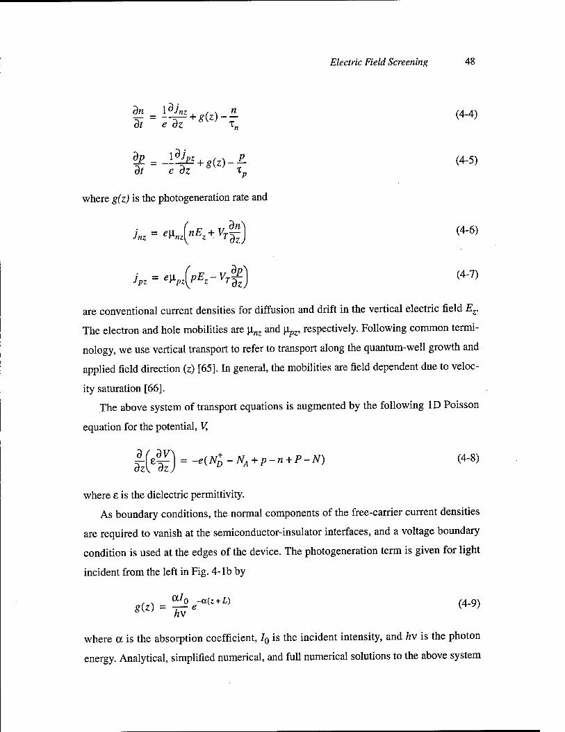
dn id/. nz
Electric Field Screening 48
+ g(z)-?- (4-4) dt e dz Xn
& = J*h + giz)-£. (4-5) dt e dz Xp
where g(z) is the photogeneration rate and
V-^-^|) <4"7)
are conventional current densities for diffusion and drift in the vertical electric field Ez.
The electron and hole mobilities are \inz and [ipz, respectively. Following common termi-
nology, we use vertical transport to refer to transport along the quantum-well growth and
applied field direction (z) [65]. In general, the mobilities are field dependent due to veloc-
ity saturation [66].
The above system of transport equations is augmented by the following ID Poisson
equation for the potential, V,
|fe|T) = -e(NZ-NA + p-n + P-N) (4-8)
where e is the dielectric permittivity.
As boundary conditions, the normal components of the free-carrier current densities
are required to vanish at the semiconductor-insulator interfaces, and a voltage boundary
condition is used at the edges of the device. The photogeneration term is given for light
incident from the left in Fig. 4-lb by
g(z) = -^e (4 »;
where a is the absorption coefficient, 70 is the incident intensity, and hv is the photon
energy. Analytical, simplified numerical, and full numerical solutions to the above system
49 CHAPTER 4
of transport equations are given. For the full numerical solutions, dark, neutral initial con-
ditions are used for the space charge, and the solutions are computed using the finite-differ-
ence discretization and second-order-implicit integration techniques described in
Appendix A.
4.2 Carrier Distributions
Starting from dark initial conditions under a DC applied voltage and uniform illumination,
the carrier densities buildup to a quasi-steady state over time scales given by the effective
carrier lifetimes. This time scale is typically on the order of nanoseconds. The screening
process, which occurs typically on the time scale of microseconds for CW illumination,
begins from the quasi-steady state carrier distributions. Many aspects of screening perfor-
mance, such as speed and resolution, are determined by the carrier distributions.
As in other shallow trap models [67], the effect of the quantum wells on the free-car-
rier densities can be described by effective transport and trapping parameters. For exam-
ple, consider the effect of quantum-well capture and escape on the transport of free
electrons. A free electron can drift in a field E0 for an average time x„, and thus a distance
\inzxnEQ, before being captured by a quantum well. Once in the well, it must wait an aver-
age time l/$N before escaping and again drifting in the applied field. Over a device of
length L, the number of these capture/emission cycles is L/[LnzxnE0, and the time for
each cycle is (xn + l/ß#)- The total transit time to traverse the device length is then
transit = TTTT^n + ^M (4"10)
If we rewrite this in terms of the effective drift velocity, vdrip such that ttransit = L/vdrift
where vdriß = \inzE0, the effective vertical mobility \inz is given by
*« = (iSkK <4-n)

Electric Field Screening 50
This is basically the free-carrier mobility weighted by the relative time spent in the con-
duction band above the barriers. Other effective transport parameters are developed below.
In the quasi-steady state regime, it is assumed that the rate of change of the carrier den-
sities is much slower than the trapping rate, and the time derivatives of the carrier densities
in the continuity equations may therefore be neglected [68]. For times short compared to
the screening time, the amount of accumulated screening charge will be negligible, leav-
ing the internal field with a uniform profile. This field is denoted -E0. In this regime, the
resulting ID carrier continuity equations can be solved analytically for the free-carrier
densities before screening begins. Making use of the quasi-steady state approximation for
both captured and free carriers, the free-electron continuity equation can be written as
2
-lfi± + L£ + n = g0{z)xRa (4-12) dz Z
where TRn = xn(l + $NiN) is an effective recombination time for the trapping of free
electrons into midgap traps, and, as will be seen, will determine the midgap trap recombi-
nation rate. This recombination time is given in terms of the well-electron trapping time
xN = l/yNNA. The interior vertical diffusion length is given by LD = J\Ln^nVT, and
the vertical drift length is given by LE = \inzT:nE0. These vertical transport lengths are
written in terms of the effective vertical mobility, \inz, and the effective free-carrier life-
time, xn. This lifetime can be found by considering the decay of the free-carrier densities
in the dark from Eqs. (4-1) and (4-4) and is given by
%n ~ XN (1+^+ßV+r) (4_13)
al0 The photogeneration rate due to the absorbed intensity is given by g0 = —. Since the
trap parameters differ near the semiconductor-insulator interfaces, the carrier lifetimes
vary in a stepwise manner.
Solutions to Eq. (4-12) are found in the drift-dominated regime, LD/LE « 1, which
is typical of semiconductor materials under normal applied voltages. Using an upwind

51 CHAPTER 4
technique [69], the solution to Eq. (4-12) along with the current density boundary condi-
tions is given to first order in LD/LE as
~i
n{z) = T^rE (e-a(z + L)_^ + L)/L£) (4_i4)
lRn
VC'RJ
(LE\ , -2aL £.
where xRn is the effective electron recombination time in the interior region, and xRn is
the effective electron recombination time in the high trap density regions near the semi-
conductor-insulator interfaces. The interior vertical drift and diffusion lengths are given by
LE and LD, respectively. The quasi-steady state free-hole density in a uniform internal
field is similar.
The two terms in Eq. (4-14) describe two separate regions of the device. These two
regions can be seen in Fig. 4-2 where the electron and hole densities are plotted for various
values of the absorption and drift length. The first term in Eq. (4-14) describes the relax-
ation of the electron density from the upstream interface as the electrons are drawn into
the device interior by the applied field. This relaxation region has a characteristic width of
LE. The second term in Eq. (4-14) describes an accumulation region as electrons collect
near the semiconductor-insulator interface. The characteristic width of this accumulation
region is given by VT/E0 and essentially represents the balance of drift and diffusion at
the interface to satisfy the no-flux boundary condition on the electron current density. For
positive applied voltage as shown in Fig. 4-2, electrons are pulled by the bias field from
the interior and accumulate at the right interface while holes accumulate at the left.
In the relaxation region, the interior carrier distributions depend strongly on the
absorption coefficient, the drift length, and the interface to which a carrier is drawn rela-
tive to the incident beam. We consider three cases in Fig. 4-2:
• LE « L, aL«l: For very short drift lengths, the carrier densities quickly rise up
from near zero at the upstream interfaces to the values determined solely by the

Electric Field Screening 52
-,12 IU 1 i i i i | i i
; 1 1 | 1 1 1 1 | 1 1 l 1 |:
1011 -: F 1' l"
u
£• 101U
<n "■"*■•-. '■ c 0) ""■s 1- a 03
109
O X \:
10B
"(a)
m7 ■
\. 1 ^ . . . . i
,12
-0.5 0 z/L
0.5
10
n"~ -m11 m E u
e T5 o
UJ
10'
i 10 c Q
,10
10s
10a
10'
: J L 1 1 1 | i i i i | i i 1 1 | 1 1 > 1 |: 1;
1 '
ji -!
,; i
1 -! 1 :
1 1
It „--"""
/! -* *^
(b) ] > 1
-1 -0.5 0 z/L
0.5 1
Figure 4-2 Quasi-steady state carrier distributions for (a)holes and (b)electrons at the start of the screening process showing the accumulation regions at the downstream interface and the relax- ation regions throughout the interior, (a) holes with the following parameters for the solid, dashed, and dot-dashed lines, respectively: ocL=3.36, LE/L=8.2; ccL=0.03, LE/L=8.2; ccL=0.03, LE/L=0.008. (b) electrons with the following parameters for the solid, dashed, and dot-dashed lines, respectively: ocL=3.36, LE/L=54; ocL=0.03, LE/L=54; ocL=0.03, LE/L=0.054. Common pa- rameters are given by: g0x^ = 6 x 1010 cm"3, TJJ/T^ = 0.1, and Vj/E0 = 8.5 nm.
photogeneration rate. For weak absorption these values are uniform and are given by go%j
and gQiRp for electrons and holes, respectively.
• LE » L, ccL«l: For very long drift lengths, the relaxation regions extend through-
out the entire device interior. The carrier densities never fully relax to the values deter-
mined by the photogeneration rate. For low absorption, the electron and hole distributions
are similar, building up throughout the interior. This monotonic buildup is due to a uni-
form photogeneration rate that constantly supplies new carriers throughout the interior.
• LE » L, ccL»l: For high absorption, carriers are only photogenerated near the front
of the device where the photogeneration rate is high, e.g. the left interface in Fig. 4-2. In
this case, the distribution of the carriers transporting to the back (electrons) and the distri-
bution of the carriers at the front (holes) are very different. The electron density builds up
from near zero at the upstream interface but then saturates in the interior since there is no
photogeneration there. The hole density builds up only at the front.

53 CHAPTER 4
Figure 4-3 Screening in the injection model showing an interior electron injecting into the surface-charge region near the semiconductor-insulator interface where it will be trapped and screen the applied voltage. The interior edge of the surface-charge region is denoted z0, and the net surface charge is Gg.
4.3 Injection Model
A basic picture of device operation can be constructed from the form of the quasi-steady
state carrier distributions. As depicted in Fig. 4-3, carriers drifting toward the interfaces
are injected into the accumulation regions and become trapped into the midgap traps. It
can be shown from Eq. (4-14) that the space charge is dominated by the collection of car-
riers in traps near the semiconductor-insulator interfaces. Since most of the space charge is
confined to the accumulation regions as an effective surface charge, the internal field
remains uniform.
The build up of the surface charge is calculated from the trapping of free carriers in the
surface-charge regions. For CW illumination, the density of the trapped charge greatly
exceeds the free-carrier density. For example, the rate equation for the surface-charge den-
sity in the electron surface-charge region is
dc >LdN, \
'z0
dz (4-15)
where the integration region is wide enough to include all of the accumulated electrons.
From the results of the previous section, this width is several VT/E0. In a properly

Electric Field Screening 54
designed device, this width will also correspond to the width, ws, of the surface-charge
region with increased trap density. In the analysis that follows, we assume that this is the
case and interchangeably refer to the surface-charge regions and the carrier accumulation
regions as the same physical regions in the device near the semiconductor-insulator inter-
faces.
Using the free-carrier continuity equations and current density boundary conditions,
Eq. (4-15) can be rewritten as
^ = 7 I +j I (4-16)
where jnz = e\inznEz and j = e[ipzpEz are the current densities from the interior,
neglecting diffusion. These currents are evaluated at the interior edge of the surface-charge
region, z0, indicated in Figs. 4-1 and 4-3, and effectively only use the relaxation term of
the carrier densities. The buildup of the surface charge thus arises from the net current
injection from the interior.
In the above analysis it has been implicitly assumed that the traps remain unsaturated
and that the lifetimes remain constant. Practically, this requires that the net trap density in
the surface-charge regions be large enough to fully screen the applied voltage. For exam-
ple, to fully screen 50 kV/cm in a device with the following parameters: L = 1.0 Jim,
d = 0.2 (im, £i = 13e0, and e2 = 5e0, the amount of surface charge required is
1 x 1012 cm"2. In this work, NSD is always selected to prevent trap saturation.
4.4 Field Screening
The screening of the internal electric field can now be calculated self-consistently by con-
sidering the field produced by the applied voltage and the screening charge. Assuming
cA = -cB = a0, as dictated by charge neutrality, the internal field, Ez, is given in terms
of the unscreened applied field,

55 CHAPTER 4
J7 — ^0
V +e2dj
and the surface charge by
Ez = XoGo-£o
where
Xo ~ K-SH
(4-17)
(4-18)
-l (4-19)
From Eq. (4-16), the rate equation for the internal field is
-%f = -*Xo(lV*(zo) + VpzP(z0))Ez (4"2°)
The resulting screening response can be characterized in terms of the vertical drift
lengths and the absorption coefficient. We consider two regimes: a short drift length
regime in which the vertical drift length is shorter than the device length, and a long drift
length regime in which the vertical drift length is longer than the device length. For both
regimes, the decay of the internal field is computed, and an analytical estimate of the ini-
tial screening rate is given.
4.4.1 Short Drift Lengths
For short drift lengths (LE«L), the injecting carrier densities are given by the photogener-
ation term since the relaxation region is so short. We consider only the low absorption case
since the combination of high absorption and short drift lengths results in a device with
poor screening behavior.
For short drift lengths and low absorption, the interior carrier densities are given by
n I = g({iRn and p I = g0^/fp • The rate equation for the internal field can then be writ- ZQ ZQ y
ten as

dIi - li dt XQ
Electric Field Screening 56
(4-21)
where
*o = [Xo(W» + Wpzgolp)] (4"22)
With the initial condition Ez = -E0, the solution to Eq. (4-21) is
Ez = -E0e-t/Xo (4-23)
This result describes screening as occurring via dielectric relaxation in which the field
decays exponentially with a time constant given by T0. This time constant is modified from
the standard dielectric relaxation time of el/(e\inzg0xn + e\ipzg0xp) by the capacitive
coupling of the applied voltage. Field screening in this regime can also be represented by a
simple equivalent circuit made of passive components [15].
4.4.2 Long Drift Lengths
For large vertical drift lengths (LE » L), the trapping of a particular carrier, either elec-
tron or hole, dominates the space charge in that carrier's accumulation region. For exam-
ple, the trapping of electrons at the right interface in Fig. 4-2 dominates the space charge
there. In addition, the assumption of antisymmetric surface charge used to develop the
previous formalism can be shown to be valid for the case of very large drift lengths. Here
we examine cases slightly outside of this regime, but still use the previous results to give
an indication of the types of screening behavior that can be obtained. Direct numerical
solutions to the transport equations can be used to obtain exact results for intermediate
regimes.
Assuming the electron and hole responses are the same, the field rate equation is:
^ - -*Wfeo)^ <4"24>

57 CHAPTER 4
400 40
4
i—i,-Li i-i- i- -L -i -t _i- ■, i ,i ,„t „
0.4 0.6 0.8 Normalized Time
1.0
Figure 4-4 Screening of the internal field for three values of the initial vertical drift length: Lz/L = 4,40,400. Time is normalized to twice the screening time for L^/L = 400.
For large vertical drift lengths, the carrier densities are themselves functions of the
field as shown in Eq. (4-14). The resulting nonlinear system must be solved numerically
with the following initial condition: Ez = -EQ. The solutions can be characterized in
terms of the initial vertical drift length, LE, and absorption coefficient, a.
Solutions to Eq. (4-24) are shown in Fig. 4-4 for various values of the initial vertical
drift length at a = 2.0xl04 cm"1. To compare time scales, EQ is held constant and the ver-
tical mobility-lifetime product is varied to obtain different vertical drift lengths. For large
vertical drift lengths the field decays at a constant rate. As can be seen from Eqs. (4-14)
and (4-24), this is due to saturation of the internal current densities. In this regime, all pho-
togenerated carriers are able to drift to the surface-charge regions without being trapped
by midgap traps in the interior, producing a response that is limited only by the photoge-
neration rate. For smaller vertical drift lengths, the response slows as carriers are trapped
multiple times in the interior as they drift to the surface-charge regions. This produces a
response that is transport-limited, and at very small vertical drift lengths the response
approaches exponential screening through dielectric relaxation as previously discussed.
The transition between the photogeneration-limited and transport-limited regimes occurs
when the vertical drift length in the interior approaches the device length. This transition
can be seen near the end of the screening process for the Lg/L = 40 case in Fig. 4-4.
Electric Field Screening 58
Normalized Initial Screening Rate
LogaL
Log LE/L
Figure 4-5 Normalized initial screening rate as a function of the vertical drift length and absorp- tion coefficient. Maximum device speed is obtained for large vertical drift lengths and large ab- sorption coefficients.
4.4.3 Initial Rate
The maximum field screening rate from Eq. (4-24) is given by e%0/0//iv. As an example,
the maximum screening rate for a device with L = 1.0 (xm, d = 0.2 |im, Ej = 13E0, e2 = 5e0
under an incident intensity of 10 mW/cm2 at 850 nm is 2 kV/cm-|is. It would thus take
-25 |is to screen a typical applied field of 50 kV/cm. The initial screening rate, assuming
equal electron and hole contributions, can be calculated for arbitrary LE and a from
Eqs. (4-14) and (4-24) as
dt V aLE
n eXohvVl-aLF t = o v t
„ -2aL -2L/LE te - e ) (4-25)
where z0~L in the evaluation of the relaxation term of the electron density.
As summarized by the plot of Eq. (4-25) in Fig. 4-5, operating at the maximum
screening rate requires large vertical drift lengths and high absorption. This can be
achieved by using moderately doped or intrinsic material to obtain long carrier lifetimes,
and by using shallow quantum wells to obtain good emission rates and large effective

59 CHAPTER 4
L=1.0um d = 0.2 pm EI = 13EQ e2 = 4.5eo
I0 = 10 mW/cm2 a = 2.0xl04 cm"1
Arjj = 2xl016cm-3 iVj) = 2xl019cm-3
JV^lxlO^crn3 iV^=lxlO,9cm-3
V0 = 20V w, = 50nm
Table 4-1 Device parameters used in the simulations. Values are typical of MQW-OASLM's like the one described in section 2.2. In particular, note the interior and surface densities of midgap traps which are used to model a moderately doped interior and low-temperature grown interface regions.
mobilities. Operating near the peak of the exciton absorption or in a non-degenerate wave-
length configuration to maximize the photogeneration rate is also desirable.
4.5 Numerical Results
In this section we examine some of the details of the screening process using direct
numerical solution of the transport equations and assess the validity of the main approxi-
mations used in the development of the injection model previously described. The two
main approximations used in the development of the injection model are the assumption
that the space charge is confined to the semiconductor-insulator interfaces as an effective
surface charge and that the electron and hole responses are the same. To investigate the
validity of these approximations, field screening was simulated in a device with the param-
eters listed in Table 4-1 and the following transport parameters: an effective electron
mobility of 64 cm2/V-s, an effective hole mobility of 18 cm2/V-s, effective interior free-
carrier lifetimes of 3 ns, and an effective surface carrier lifetime of 10 ps. As described in
section 4.2, these effective parameters describe carrier transport in the shallow trap model

Electric Field Screening 60
1
0
i ■ 1 ■ i ■ 1 i
■J ■
1
-1
o -2 LU
\
in -3 7 -
-4 : -
-5 :
i i ■ -o -1.2 -0.8 -0.4 0 0.4 0.8 1.
z (um)
Figure 4-6 Interior field distribution showing good uniformity. Most of the variation occurs near the semiconductor-insulator interfaces in the surface-charge regions.
for quantum wells. These parameters were chosen from typical values for AlGaAs trans-
port and quantum-well properties [70, 71], and from carrier escape calculations in
Chapter 3.
We first examine the uniformity of the interior field. In Fig. 4-6, the vertical profile of
E along the device length is shown midway through the screening process. The profile is
quite uniform, with most of the variation occurring in the surface-charge regions near the
interfaces. This supports the basic surface charge picture presented above.
To examine the validity of the screening results calculated using the injection model
with equal surface-charge screening rates for electrons and holes, field screening using the
device parameters above was computed using the injection model and simulated using
direct numerical solutions to the transport equations. A comparison of the results in
Figure 4-7 shows that the computed responses agree quite well, with the small discrepancy
attributable to the different electron and hole parameters. For the injection model calcula-
tion, an electron/hole mobility-lifetime product of 2.0xl0"7 cm2/Vs was used. The agree-
ment in Fig. 4-7, especially at short times, indicates that Eq. (4-24) is indeed a good
estimate of the screening rate for typical parameters.

61 CHAPTER 4
E o
0 Li.
Full Numerical Injection Model
0.5 1 Time (ms)
1.5
Figure 4-7 Comparison of the screening responses calculated using the injection model and full numerical solutions to the transport equations. The discrepancy as the field decays to zero is attrib- uted to the different electron and hole transport parameters which the injection model does not consider.
4.6 Semiconductor and Quantum-Well Effects
There are a number of unique effects that occur in semiconductor and quantum-well mate-
rials that we have neglected up to this point but which can have a large impact on transport
behavior. These effects include velocity saturation, resonant absorption, QCSE absorption,
and field dependent carrier emission from the quantum wells. The impact of each of these
effects can be considered within the framework of the injection model.
The saturation of the drift velocity of electrons in bulk GaAs in fields above 4 kV/cm
is a well known phenomenon [66]. Holes also display drift velocity saturation at larger
fields. Drift velocity saturation describes the crossover of the drift velocity from linear
behavior at low fields to a saturated value at high fields. In bulk GaAs at room tempera-
ture, this saturation effect is caused by increased phonon scattering as the carriers gain
kinetic energy from the field and from &-space transfers to different parts of the Brillouin

Electric Field Screening 62
0
LI " ^
0
u - ^ ^nz 0 r , n
1 + KzEz/vsat 1+VpzEz/vsat
Ll°.,= 2000cm2/Vs Ll°z=150cm2/Vs
v"ßf=1.0xl07cm/s vfa,= 1.0xl07cm/s
Table 4-2 Velocity-saturated mobilities. The low field mobilities and saturation velocities are typi- cal of AlGaAs alloys. The simple functional dependence of the mobilities is typical of velocity- saturated mobilities for holes in bulk GaAs.
zone that have lower mobilities. The exact form of velocity saturation in MQW materials,
however, is not so well understood. Recent studies at moderate fields (< 30 kV/cm) show
no clear signs of velocity saturation [72] while studies at higher fields show clear evidence
of velocity saturation [50]. For vertical transport, velocity saturation serves to limit the
vertical drift length. Depending on the quantum-well escape rates and the carrier lifetimes,
the screening response can be pushed into the transport-limited regime if the saturated
drift velocity is small enough.
The simplest way to incorporate velocity saturation into the drift-diffusion model is to
use a field dependent mobility [64]. As an example, Table 4-2, gives a relatively simple
velocity saturation model in which the low field mobilities are constant while the high
field mobilities go like \IE where E is the field. The values for the low field mobilities and
the saturated drift velocities are typical of bulk GaAs [70,76]. The functional dependence
of the hole mobility on the field is also typical of bulk GaAs. The electric field dependence
of the electron mobility, however, is a simplification of the bulk GaAs mobility, and while
it does not include negative differential resistance at low fields, the high field behavior is
similar to that of the bulk GaAs mobility.
Figure 4-8 shows the screening response calculated using the mobilities from
Table 4-2 and the device parameters from Table 4-1. For comparison, the screening

63 CHAPTER 4
E o >
I I I I I
Constant mobility Velocity saturation
0.5 1 Time (ms)
1.5
Figure 4-8 Comparison of field screening calculated using constant mobilities and velocity- saturated mobilities. In this example, the long carrier lifetimes and large effective mobilities keep the velocity-saturated response in the photogeneration-limited regime.
response calculated using constant mobilities is also shown. Since the effective carrier
lifetimes are sufficiently long and the effective carrier mobilities are sufficiently high in
this example, the velocity-saturated screening response still follows the basic
photogeneration-limited behavior. As long as the vertical drift lengths remain much longer
than the device length, the initial screening response will be fairly insensitive to the actual
mobility values. We will see in later chapters that the main effect of velocity saturation is
on the resolution performance.
The presence of quantum wells presents a number of new transport properties in addi-
tion to those of bulk transport. We have already considered the effective carrier lifetimes
and mobilities due to the escape from and capture by the wells. Another property of quan-
tum-well transport is the ability to photogenerate well carriers through resonant absorption
between valence and conduction subbands. The injection model can be straightforwardly
modified to include resonant absorption instead of non-resonant absorption across the bar-
rier bandgap. This requires moving the photogeneration term from the free-carrier conti-
nuity equations to the well-carrier continuity equations. The field screening results found

Electric Field Screening 64
with these modifications are actually the same as those found for non-resonant absorption,
except that the effective photogeneration rate for free electrons is
(The result for holes is similar.) This is essentially the resonant photogeneration rate mul-
tiplied by the escape probability of a well-confined electron. For small escape rates, this
reduces the generation of free electrons and hence the screening rate.
Another unique quantum-well property is the quantum confined Stark effect, which is
used primarily as an electro-optic effect as discussed in Chapter 3. However, since it pro-
duces a field dependent absorption coefficient for resonant illumination, it directly affects
the photogeneration rate. The effect on the actual screening rate, however, depends on the
absorption length. For low absorption, the screening rate given from Eq. (4-25) is directly
proportional to the absorption coefficient, and thus the changing QCSE absorption will
result in a constantly changing response rate. For high absorption, however, the screening
rate is independent of the absorption coefficient, and as long as the absorption remains
high throughout the screening process, device operation will be unaffected by the QCSE.
The final quantum-well property we consider is the field dependence of the carrier
escape rates from the quantum wells. As discussed in Chapter 3, the thermionic emission
and tunneling rates depend strongly on the field. For example, the electron escape rate
shown in Fig. 3-9 decreases by almost two orders of magnitude as the field is reduced
from 100 kV/cm to 40 kV/cm. For typical parameters, the effective carrier mobilities
depend linearly on the carrier escape rates as shown in Eq. (4-11). Therefore, a drastic
reduction in the escape rate could plunge the device into the transport-limited regime and
slow down the screening response.

65 CHAPTER 4
4.7 Summary
In summary, we have developed a one-dimensional drift-diffusion model to simulate the
screening of the internal electric field in a MQW-OASLM. Quantum wells were included
explicitly using a shallow trap model and were shown to partly determine the operating
regime through the effective free-carrier mobilities and lifetimes. Analytical calculations
of the quasi-steady state carrier distributions were shown to justify the often used surface-
charge picture of device operation. The separation of the carrier distributions into relax-
ation and thin accumulation regions was used to develop an injection model of device
operation. In this model, screening occurs through the injection of interior carriers into
thin surface-charge regions near the semiconductor-insulator interfaces. Using this model,
two screening regimes were identified: transport-limited and photogeneration-limited. For
vertical drift lengths shorter than the device length (transport-limited), screening proceeds
via dielectric relaxation. The maximum screening rate, however, is obtained for long verti-
cal drift lengths (photogeneration-limited) where the field screens down at a constant rate.

Chapter 5
Transmission and Photocurrent Response
The most common technique used to investigate screening behavior in quantum-well
devices is the measurement of the optical transmission at wavelengths resonant with the
quantum confined Stark effect. Assuming the field dependence of the QCSE is known, the
internal field can be extracted from the measured transmission through an inversion pro-
cess. Variations of this technique has been used to study a number of interesting topics in
quantum-well devices including carrier escape from wells [65], short-pulse
screening [73], and the speed response of optical modulators [74].
The primary advantage of measuring the optical transmission is that it provides a sim-
ple, indirect way of determining the behavior of the internal field, which is typically the
quantity of interest when designing optical modulators. One of the main drawbacks of this
technique, however, is that, to lowest order, the QCSE is quadratic in the field and there-
fore has poor differential sensitivity at low fields. In the MQW-OASLM this can be prob-
lematic since the internal field is expected to be fully screened. The transmission is not the
only means of characterizing screening behavior, however. During the screening process, a
transient photocurrent flows as the internal space charge is created. This photocurrent is a
displacement type of current and is linear in the time derivative of the internal field, pro-
viding better sensitivity at low fields.
In this chapter we compare experimentally measured screening behavior to the screen-
ing response calculated using the device model presented in the previous chapter. Both the
66

67 CHAPTER 5
transmission and photocurrent are used to determine the electric field screening rate,
examine the polarity dependence of device operation, and demonstrate the characteristic
responses of the photogeneration-limited and transport-limited regimes described in the
previous chapter. For the device simulation, realistic device parameters from the literature
and the carrier escape calculations in Chapter 3 are used. In general, very good qualitative
agreement is found. In addition, a number of more subtle transport effects, including the
relative contribution of each of the carriers to the screening process and the effect of
velocity-saturated carrier mobilities on the photocurrent, are examined.
5.1 Experiment
The only experimental investigation of the response of a MQW-OASLM under uniform
illumination has been presented by Partovi et al. [6] who measured the transmission as a
function of the frequency of an applied square wave voltage. The response at only one
voltage amplitude was measured. In addition, comparing frequency dependent measure-
ments to intensive time-domain simulations is not very convenient. In this section we sum-
marize time dependent measurements that we have performed on the sample described in
Fig. 2-5. The experiments involved applying a bipolar square wave voltage to the sample
and measuring the resonant transmission and photocurrent responses. Each transition of
the square wave initiated a new screening processes as photogenerated carriers were
driven to the opposite interface. This presented a convenient way of studying the screening
response for both polarities as well as for various amplitudes of the applied voltage.
The photocurrent that flows during the screening process is a displacement type of cur-
rent. It can be viewed as the residual charging current that is required to maintain a con-
stant voltage across the device as the internal space charge is created. Assuming the device
structure is symmetric, this photocurrent is related to the internal voltage created by the
screening charge, Vscn as
I = -y»-äf (5-1)

Transmission and Photocurrent Response 68
where Q, is the capacitance of the insulating layers. This capacitance is determined by the
illuminated area of the sample. The photocurrent is linearly proportional to the time deriv-
ative of the screening-induced voltage and thus provides extra sensitivity to the screening
dynamics.
5.1.1 Setup
Figure 5-1 shows the experimental setup used to simultaneously measure the transmission
and photocurrent. The sample was illuminated with a HeNe laser operating at a wave-
length of 632.8 nm. The HeNe beam was spatially filtered and expanded to provide a uni-
form beam profile. A square aperture with an area of 7 mm2 was placed in front of the
sample to give a well defined area for the photocurrent calculations. HeNe at 632.8 nm
was chosen as the photogenerating wavelength since its absorption coefficient of
3xl04 cm"1 is quite high and thus useful for separating the relative contributions of the car-
riers in the screening process. The modeling is also simplified since this wavelength is not
resonant with the QCSE, and the stability and low drift of the intensity allow the direct
comparison of results taken over several hours.
The sample was driven by a bipolar square wave applied voltage from a function gen-
erator with no DC offset. The drive frequency was set low enough to allow the screening
process to run to completion during each half period. The polarity convention used in the
experiment and in the analysis is indicated in Fig. 5-1 in which the front of the sample rel-
ative to the incident beam was connected to the ground path.
The transmission of the sample was measured with an IR probe beam from a
lamp/monochromator arrangement. The quartz-halogen lamp and monochromator pro-
vided a convenient source of low power, tunable IR wavelengths. The lamp was also very
stable which allowed for easy normalization of the transmission from run to run. To
reduce stray light, a box was placed around the input path to the monochromator, and an
IR passing filter was placed in front of the detector. A silicon photodiode/amplifier combi-
nation with a gain of 1.2xl07 V/W and a bandwidth of 35 kHz was used to measure the
transmitted IR beam. A schematic of the amplifier is shown in the appendix to this chapter.

69 CHAPTER 5
Tungsten-Halogen Lamp
Light Box
Photodiode
Figure 5-1 Experimental setup for measuring the transmission and photocurrent. The sample is il- luminated by a spatially filtered and expanded HeNe beam to photogenerate carriers. The trans- mission of an IR probe beam from the lamp/monochromator arrangement is measured with a photodiode/amplifier combination. The sample is driven with a bipolar square wave voltage from the function generator, and the return path to ground is through a 50 ß resistor through which the photocurrent is measured. As a polarity convention, the front of the sample relative to the incident HeNe beam is taken as the grounded side.

Transmission and Photocurrent Response 70
The photocurrent was measured through a 50 Q series resistor in the return path to
ground. Each half period of the applied square wave produced a current signal with two
components. The first component is due to the charging of the total device capacitance
immediately after the polarity is switched. The time constant for this charging process is
given by the series resistance of the current measurement resistor and the output imped-
ance of the function generator, and the device capacitance. The device capacitance was
1.2 nF, and for the parameters used in this setup, the RC time constant was 122 ns.
The charging component is followed by a much smaller and more slowly developing
signal that is due to the displacement current produced during the screening process. The
magnitude of this current component can be 100 times smaller than the charging transient.
To measure the screening component without overloading the downstream electronics
with the charging transient, output clamping amplifiers were used. The schematics for
these amplifiers are also shown in the appendix to this chapter. The total current signal that
was measured thus consisted of the sum of the screening current and a clamped version of
the charging transient. To remove the charging transient and any background bias signal,
the dark response measured without HeNe illumination was subtracted from the response
measured with HeNe illumination. It should be noted that the resulting current signal dur-
ing the period of the charging transient (the first 0.5 [is) cannot be reliably used as an indi-
cator of the screening component since the voltage across the sample is constantly
changing.
The outputs of the photodiode/amplifier combination and the current amplifier were
sampled using a LeCroy Model 6810 Waveform Recorder. This is a 12 bit A/D system
with a bandwidth of 2.5 MHz and a maximum sampling rate of 2 Msamples/s. Typically,
the average of 100 consecutive periods was calculated to improve the signal to noise ratio.
5.1.2 Transmission Results
In order to extract the screening behavior of the internal field from the transmission mea-
surements, it is first necessary to calibrate the transmission change induced by the QCSE.
This then allows the measured transmission values to be converted into internal field

71 CHAPTER 5
I °-8 w "E to c CO
0.6
"S 0.4 N
"ÖS E o 0.2
■J—I—I—I—I—1—1 ■_! I—I L_J t_ I ■ ... 1 ■ ' ■ ■ ■ ■ ' ■ ■ ■ ■
0 5 10 15 20 25 30 35 40 Field (kV/cm)
Figure 5-2 Transmission as a function of internal field due to the QCSE without screening. The transmission is normalized by the zero field value. This curve is used to convert the measured transmission during screening into internal field values.
values. This calibration was performed by measuring the transmission of the IR probe
beam without HeNe illumination as a function of the applied voltage. The IR beam had a
power of 100 nW and was tuned to the peak of the QCSE differential transmission at
852 nm with a monochromator resolution of 1 nm FWHM. For this measurement, the
sample was driven by a bipolar sawtooth applied voltage at 200 Hz to provide a conve-
nient means of scanning through the desired voltage range. An alternating applied voltage
is required since a DC voltage would eventually become screened by thermal generation
and by optical generation from the IR probe beam. A measurement of the transmission
with a square wave applied voltage at 200 Hz showed no evidence of screening effects,
indicating that any screening contributions from thermal or IR generation were negligible
during the time scales of the experiment. The calibration of the QCSE obtained after con-
verting the applied voltage to electric field and normalizing the transmission by the zero
field value is shown in Fig. 5-2.
For the actual screening measurements, the transmission under HeNe illumination at
an intensity of 1.6 mW/cm was measured for both polarities and various amplitudes of
the applied square wave voltage at a drive frequency of 200 Hz. The IR probe wavelength

Transmission and Photocurrent Response 72
Time (ms)
Figure 5-3 Screening of the internal electric field as determined from the measured transmission for the indicated peak-to-peak applied voltages during the positive half-period of the applied volt- age. The time origin occurs at the switching of the applied voltage from negative to positive polar- ity.
and power were the same as used is the QCSE calibration. The transmission under short
circuit conditions was used to normalize the resulting transmission curves, and the QCSE
transmission calibration from Fig. 5-2 was then used to find the corresponding field val-
ues.
The results for three applied voltage amplitudes during the half period of positive
polarity of the driving voltage are shown in Fig. 5-3. For all applied voltages, the initial
decay is very linear at a rate of 55 kV/cm-ms. Also, for all applied voltages the internal
field is completely screened down to zero. This indicates that the insulating barriers are
confining the carriers to the interior region as desired. If there were significant and contin-
uous leakage through the barriers, the screening would be incomplete since the voltage
drop across the device would be divided between the semiconductor and insulator regions
in proportion to their effective resistivities [14]. As the photocurrent response will show,
however, there does appear to be a small amount of leakage current flowing at larger
applied voltages. The transmission measurements, however, indicate that this current is
not large enough to prevent complete screening.

73 CHAPTER 5
The completeness of the screening also indicates that the trap density at the
semiconductor-insulator interfaces is sufficient to hold the screening charge without satu-
rating. If the traps were saturated or there were significant bulk charge, the screening could
not run to completion, and the field would not decay in a linear fashion.
The initial screening rate was also measured as a function of incident intensity from
1 mW/cm to 10 mW/cm and was found to be linear. This is in general agreement with
the results of Chapter 4.
Implicit in the conversion process from transmission to internal field is the assumption
that the internal field is uniform within the quantum-well region. The extreme linearity of
the field decay, the completeness of the screening process, and the surface-charge model-
ing results from Chapter 4 indicate that this is an accurate assumption.
5.1.3 Photocurrent Results
As indicated in Eq. (5-1), the photocurrent is proportional to the time derivative of the
internal voltage and thus provides better sensitivity than the transmission to the screening
dynamics. This additional sensitivity is especially useful in examining the approach to full
screening. The details of the screening behavior in this low field region are essentially lost
in the transmission measurements.
The photocurrent response under the same illumination conditions as for the transmis-
sion results are shown in Fig. 5-4 for a more complete set of applied voltages at positive
polarity. For low voltages, the response decays quickly. For large voltages, the response
consists of three regions: a fast initial transient, a plateau, and finally a decay. The fast ini-
tial transient was not seen in the transmission data and may be due to some form of tran-
sient leakage current. In the plateau region, the initial photocurrent saturates for large
voltages. From Eq. (5-1), this indicates that the decay of the internal voltage, and hence
field, is linear. This agrees with the results of the transmission measurement. The time for
the onset of the photocurrent decay depends approximately linearly on the applied voltage
while the time scale for the actual decay appears to be independent of the applied voltage.

Transmission and Photocurrent Response 74
20
15
<
r- 10 c
ü
' ' ll \
■ 1V
■ 2v : — • 4V -
:'.v > \ • 1
»s^v«, ■ 8V ■ 1
-• 1 . 1
■ 1
-• I
\ -12V
■
1 1
1 1
\
i \ V \ \ \
""•»v *•.„, ^^m " " ***■"*•*—....
-
_J 1 L S
0.5 1 Time (ms)
1.5
Figure 5-4 Measured photocurrent for the indicated peak-to-peak applied voltages, positive polar- ity. The time origin occurs at the switching of the applied voltage to positive polarity.
At longer times, the photocurrent response shows an offset which may also be due to leak-
age currents.
The photocurrent response also depends on the polarity of the applied voltage as
shown in Fig. 5-5 where the photocurrent for positive and negative half-periods of the
applied voltage are shown for two peak-to-peak voltages. In Fig. 5-5a, the response with a
relatively low peak-to-peak applied voltage of 4 V is shown. The photocurrent responses
for the two polarities are asymmetric with a slightly faster response obtained for positive
polarity. This polarity draws electrons to the back of the device relative to the incident
beam. This can be compared to the result for a larger peak-to-peak voltage of 12 V, shown
in Fig. 5-5b, for which the negative polarity displays an initially faster response.
Similar differences in the transmission results were also seen as a function of polarity,
although they were not as pronounced as those seen in the photocurrent results. This sug-
gest that, although there may be some leakage current present in the photocurrent mea-
surements, the differences in the photocurrent responses as a function of polarity are due
to screening effects and not to excess leakage current. We have also examined one sample
in which no initial fast transients were seen, yet similar asymmetries due to polarity were
still present.

75 CHAPTER 5
(+) Polarity (-) Polarity
(a) S 3 o
20
15
10
5
—(+) Polarity (-) Polarity ■
\ \ (b) :
s\ ■
i . . . . ""
0.4 0.6 0.8 Time (ms)
0.5 1 Time (ms)
1.5
Figure 5-5 Measured photocurrent response for both polarities of the applied voltage for a peak- to-peak voltage of (a) 4 V and (b) 12 V. The negative polarity response has been inverted for com- parison.
5.2 Simulation
The transient decay of the internal field and the displacement photocurrent can be calcu-
lated using the device model presented in the previous chapter. In order to consider the
complete screening response and also nonlinear transport effects such as velocity satura-
tion, we use direct numerical solutions to the transport equations. The field decay is used
to compare simulated and measured screening rates, and the photocurrent response is used
to examine some of the more subtle transport behavior. Of particular interest is the asym-
metry of the photocurrent response for various polarities and amplitudes of the applied
voltage.
5.2.1 Device Model
Field screening was simulated using the ID device model described in Chapter 4 with the
parameters listed in Table 5-1. These parameters were taken from the literature, from the
results of the carrier escape calculations in Chapter 3, and from the device geometry
shown in Fig. 2-5. In the simulation, the device geometry consisted of a 2.09 fim quan-
tum-well region, a bulk-like 1500 Ä etch stop region, and 50 nm surface-charge regions
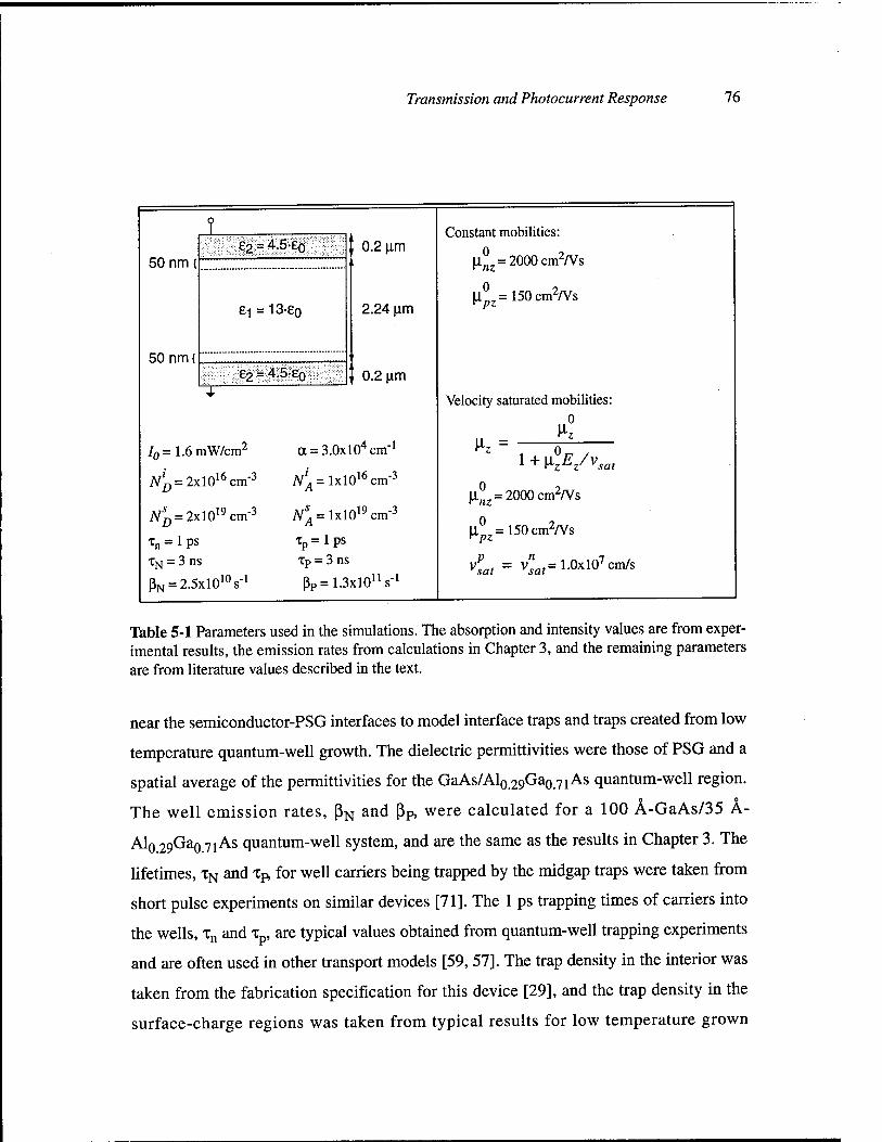
Transmission and Photocurrent Response 76
50nm{
50 nm{
E2 = 4.5-eo
El = 13-e0
e2 = 4.5-£o
:: 0.2 um
2.24 um
0.2 (im
I0= 1.6 mW/cm2
^ = 2xl016cm"3
A^ = 2xl019cm-3
Tn=lps
% = 3 ns
ßN = 2.5xl010s"1
a = 3.0xl04cm_1
N\ = lxl016cm'3
N\ = lxlO19 cm"3 k tp = 1 ps xP = 3 ns
ßp = 1.3xl011s-1
Constant mobilities:
nDz = 2000cm2/Vs
H,°z=150cm2/Vs
Velocity saturated mobilities: 0
0 i + Mz/v. sat
JInz = 2000cm2A^s
(IpZ=150cm2A^s
vL = V^=1.0xl07cm/s
Table 5-1 Parameters used in the simulations. The absorption and intensity values are from exper- imental results, the emission rates from calculations in Chapter 3, and the remaining parameters are from literature values described in the text.
near the semiconductor-PSG interfaces to model interface traps and traps created from low
temperature quantum-well growth. The dielectric permittivities were those of PSG and a
spatial average of the permittivities for the GaAs/Al0 29Ga0 71As quantum-well region.
The well emission rates, ßN and ßp, were calculated for a 100 Ä-GaAs/35 Ä-
Al0 29Ga0 71As quantum-well system, and are the same as the results in Chapter 3. The
lifetimes, % and TP for well carriers being trapped by the midgap traps were taken from
short pulse experiments on similar devices [71]. The 1 ps trapping times of carriers into
the wells, Tn and xp, are typical values obtained from quantum-well trapping experiments
and are often used in other transport models [59, 57]. The trap density in the interior was
taken from the fabrication specification for this device [29], and the trap density in the
surface-charge regions was taken from typical results for low temperature grown

77 CHAPTER 5
AlGaAs [75]. The acceptor compensation ratio was set to 0.5 since trap saturation was not
a concern in the operating regime being considered.
Simulations using constant mobilities and simulations using velocity-saturated mobili-
ties were both performed. The values of the low field mobilities and the saturated drift
velocities are typical for AlGaAs [70]. The field dependence of the mobilities was the
same as that used in section 4.6. The effective low field mobility-lifetime products for
electrons and holes were 1.5xl0"7 cm2/V and 6.0xl0"8 cm2/V, respectively. The absorp-
tion coefficient and incident intensity were measured experimentally. The intensity in the
interior, however, is reduced by the reflectivity of the front gold/PSG layers. The reflectiv-
ity was estimated using a stacked-slab dielectric model to be approximately 80%.
The simulations were started from dark, neutral space-charge initial conditions and run
using the following sequence of applied voltages: +V0, -V0, +V0. This models the bipolar
square wave applied voltage used in the experiments. The time for each voltage segment
was long enough to allow the simulation to reach steady-state before the polarity was
switched. The displacement photocurrent through the insulating barriers was calculated
for comparison to the photocurrent measurements.
5.2.2 Field Screening Results
The screening of the internal field was simulated using constant mobilities and the same
applied voltages used in the measurements summarized in Fig. 5-3. The results are shown
in Fig. 5-6. As with the experimental results, the initial screening behavior is linear with
all voltage cases decaying at the same rate. The time scales for complete screening also
agree well with the experimental results. The approach to full screening is more gradual
than in the experimental results, but the transmission measurement is not very sensitive at
such low fields. The approach to full screening will be examined more carefully using the
photocurrent measurements.
The screening behavior seen in the experimental and simulation results is indicative of
the large drift length regime described in Chapter 4. In this regime, a saturated internal
photocurrent produces a constant screening rate. For large vertical drift lengths, the

Transmission and Photocurrent Response 78
OO
12V : 30 --•10V :
\ \ 8V : 25 - ^ \ -
E \ \ . .0 > 20 : *. \ \ ■j .j»; •. \ \ ' T3 15 \ \
" ^ \ -
(1) II '. \ \ ■
10 - ^ \ - \ \ .
•. \ \ ■
5 •. \ \ - •. \ \ •
n ' ' "'* -■- ^" w-Z^a»_i 1 1_
0 0.5 1 Time (ms)
1.5
Figure 5-6 Simulated field screening using constant mobilities for the indicated peak-to-peak voltages at positive polarity. The initial linear behavior and screening rate agree well with experi- mental results.
screening rate can be estimated from the injection model result in Eq. (4-25) with the
parameters in Table 5-1. The calculated rate of 50 kV/cm-ms agrees well with the experi-
mental results.
5.2.3 Photocurrent Results
As discussed in Chapter 4, the initial screening behavior in the large vertical drift length
regime is not very sensitive to the mobility. The simulated approach to full screening,
however, does depend on the mobility model through the dielectric relaxation time. We
therefore consider two different models, one with constant mobilities and one with
velocity-saturated mobilities.
The simulated photocurrent response using the constant mobilities listed in Table 5-1
is shown in Fig. 5-7. The photocurrent was simulated for positive polarity using the same
applied voltages used in the experiments. The behavior agrees qualitatively with the exper-
imental results. The initial photocurrent saturates when the applied voltage reaches
approximately 8 V. The initial photocurrent values, however, are slightly different than the
experimental values in Fig. 5-4. This discrepancy may be due to small leakage currents

79 CHAPTER 5
15
< 10
c
ü 5
: — iv ; ■ — - 2V : ■ --■ 4V - 8V :
12V ;
\\\ \ \ ■
v \ \ \ :
: \ v \ 4«
0.5 1 Time (ms)
1.5
Figure 5-7 Simulated photocurrent response using constant mobilities for the indicated peak-to- peak voltages at positive polarity. The decay of the current signal is due to the transition from the long drift length regime to the dielectric relaxation regime.
and/or slight errors in some device parameters, such as the dielectric permittivity of PSG
which depends upon the details of the fabrication process.
From the results of the injection model described in Chapter 4, the decay of the photo-
current for large applied voltages at positive polarity occurs when the electron drift length
approaches the device length, or, equivalently, when the mean transit time of electrons
across the interior, as given by L/\LnzE, becomes longer than the effective electron life-
time. As the transit time becomes longer than the effective lifetime, the photocurrent tran-
sitions from the saturated regime into the dielectric relaxation regime. When the transit
time is much shorter than the lifetime, electrons quickly drift to the back interface without
being trapped in the interior and contribute efficiently to the screening process. For long
transit times, electrons are trapped many times in midgap traps before reaching the back.
In fact, for high absorption, the electron current in the back of the device is greatly reduced
since electrons trap in regions of reduce optical intensity. A similar effect has been seen in
the photocurrent of MQW p-i-n photodiodes when the carrier transit times across the
intrinsic region become greater than the carrier lifetimes [72].

Transmission and Photocurrent Response 80
(+) Polarity (-) Polarity Back carrier n=0
(a)
0.4 0.6 0.8 Time (ms)
(+) Polarity (-) Polarity
0.5 1 Time (ms)
Figure 5-8 Simulated photocurrent response for both polarities using constant mobilities at peak- to-peak voltages of (a) 4 V and (b) 12 V. In (a) the dotted-dashed curve shows the effect of sup- pressing the mobility (|i) of the back carrier and is the same for both polarities.
The effect of the carrier transit time across the MQW region on the photocurrent
response can be seen in Fig. 5-8a which shows the simulated photocurrent for a moderate
applied voltage (4 V peak-to-peak) for both polarities. The asymmetry in the response is
qualitatively similar to the experimental result in Fig. 5-5 and shows how the photocurrent
depends on which carrier is drawn to the back. Drawing the carrier with the largest
mobility-lifetime product (electrons) to the back produces a slightly faster response since
this pushes the device more into the saturated photocurrent regime. This produces a larger
initial current and a slightly faster decay. The sensitivity of the photocurrent to the back-
drifting carrier is also been seen in Fig. 5-8a. The photocurrent response was simulated
with the mobility of the back-drifting carrier set to zero for either polarity. For this case,
the photocurrent is drastically reduced. This emphasizes the sensitivity of the response to
the back-drifting carrier and provides convincing evidence for bipolar transport.
The simulated photocurrent response using constant mobilities and a large peak-to-
peak voltage (12 V) is shown in Fig. 5-8b for both polarities. As in the simulated 4 V case,
the photocurrent for positive polarity displays a slightly faster response. However, this
does not agree with the experimental results in Fig. 5-5b. Also, the decay of the simulated
responses is somewhat sharper than the experimental results. One possible explanation for
these two discrepancies is velocity saturation. As discussed in Chapter 4, velocity

81 CHAPTER 5
20
15
<
~ 10 0 X-
3 Ü
1 1 ' r ~i™i—i—i—i—i
iv : 2v :
" ---4V - ■ -—8V ■ 12V -
■
• \ \
--. '. * -
■ •. '. \
'■-■»•--■-
0.5 1 Time (ms)
1.5
Figure 5-9 Simulated photocurrent response using velocity-saturated mobilities for the indicated peak-to-peak voltages at positive polarity. The decay of the current signal is more gradual than in the constant mobility case.
saturation is a prominent transport effect in bulk GaAs at high fields and is expected to
also be so for MQW devices [52].
The velocity saturation of electrons and holes occurs at widely different fields
(~4 kV/cm for electrons and -30 kV/cm for holes), and this can lead to an unusual photo-
current response depending on the applied voltage and polarity. Here we investigate the
effect of a simple velocity saturation model in order to qualitatively show how velocity
saturation might affect the photocurrent response. Figure 5-9 shows the simulated photo-
current series for positive polarity using the velocity saturation model summarized in
Table 5-1. The decay of the velocity-saturated photocurrent occurs at times similar to
those found for the constant mobility case, but the decay is more gradual and more like
that seen in the experiments.
As shown in Fig. 5-10, the polarity dependence of the photocurrent simulated using
velocity-saturated mobilities also agrees better with the experiments. At low voltages, the
ordering of the faster polarity is the same as for the constant mobility case: positive polar-
ity produces a slightly faster response. At such low voltages, velocity saturation has not
significantly reduced the electron mobility, leaving the electron mobility-lifetime product

Transmission and Photocurrent Response 82
15 (+) Polarity (-) Polarity
0.4 0.6 Time (ms)
15
10
c 0)
5 5 Ü
-(+) Polarity •(-) Polarity
0.5 1 Time (ms)
Figure 5-10 Simulated photocurrent response for both polarities using velocity-saturated mobili- ties at peak-to-peak voltages of (a) 4 V and (b) 12 V. Note that initially, the faster response in (a) occurs at positive polarity while the faster response in (b) occurs at negative polarity.
larger than the hole mobility-lifetime product. However, at larger voltages, as shown
Fig. 5-10b, the faster polarity (i.e. carrier) changes as the reduction of the electron mobil-
ity by velocity saturation pushes the electron mobility-lifetime product below that of the
holes.
The velocity-saturation model which produced Figs. 5-9 and 5-10 was chosen for sim-
plicity. While the field dependence of the hole-mobility in Table 5-1 is actually similar to
the field dependence of the hole mobility in bulk GaAs [76], the exact mobility models for
vertical transport in GaAs/AlGaAs quantum wells are not known. The general trends of
the experimental data, however, are explained by this simple velocity saturation model. In
principle, other field dependent effects, most notably carrier escape from wells, could also
produce an unusual photocurrent response as a function of field. In the case of carrier
escape, however, the field dependence over the voltage range under consideration is too
weak to explain the observed effects. As will be discussed in Chapter 7, the field depen-
dence of the carrier escape rates will play an important role in determining device resolu-
tion.

83 CHAPTER 5
5.3 Summary
The frame rate of the MQW-OASLM is essentially determined by the screening response
under uniform illumination. Accurate estimates of the screening rate are required to opti-
mize trade-offs in device design. In this chapter, optical transmission and photocurrent
measurements were used to verify the screening rate calculations in Chapter 4. In addition,
the photocurrent measurement described in this chapter was shown to be a particularly
sensitive probe of some of the more interesting transport dynamics, including the transi-
tion between photogeneration-limited and transport-limited regimes. Evidence for bipolar
transport was found using the photocurrent measurement, and an asymmetric response to
polarity under high absorption was attributed to the different mobility-lifetime products of
the electrons and holes. Finally, a simple velocity-saturation model was used to explain an
unusual photocurrent response at high voltages.
5.4 Appendix
In this appendix, the various homemade amplifiers used in the transmission and photocur-
rent experiments are described. These amplifiers were designed to meet the specific gain
and bandwidth requirements for the particular time scales and intensity levels in the exper-
iments. In the case of the current amplifiers, output clamping was an important feature to
prevent overloading of the downstream A/D system.
The photodiode amplifier shown in Fig. 5-1 la uses a Hamamatsu model S1223-01 sil-
icon photodiode which has an area of 13 mm2 and a responsivity of 0.6 AAV" at 850 nm. It
is reverse biased to maintain a small capacitance. The current from the photodiode is
amplified by a two stage amplifier. The first stage consists of a transimpedance amplifier
with a gain of 10 V/A. A 5 pF parallel capacitor is used to prevent ringing, and a DC cur-
rent bias is provided at the input. This stage is followed by a simple inverting voltage
amplifier with a gain of 20. The overall gain of the system is 1.2xl07 VAV at 850 nm with
a 3 dB bandwidth of 35 kHz.

Transmission and Photocurrent Response 84
a) Photodiode amplifier
2KQ.
100 n J-AAV-L
G = 2x10⁷V/A
f3dB = 35KHz
-15V
b) Low gain amplifier for current measurements
50Q
G = 757 V/A
f3dB>20MHz
c) High gain amplifier for current measurements
500 Q VvV-
G = 2.7x10s V/A
f3dB = 340KHz
:: y. 1N4148
Figure 5-11 Schematic diagrams of the homemade amplifiers used in the transmission and photo- current experiments. The photodiode amplifier in (a) was used in the calibration of the QCSE and in screening measurements. The low gain, large bandwidth amplifier in (b) was used to investigate large initial transients in the photocurrent response. The higher gain, smaller bandwidth amplifier in (c) was used for the majority of the photocurrent measurements presented in this chapter.

85 CHAPTER 5
Two different amplifiers were constructed to amplify the current signal passing
through the 50 Q resistor in series with the sample. The circuit shown in Fig. 5-1 lb con-
sists of a fast, output clamping Comlinear 501 amplifier in a simple non-inverting configu-
ration. A 50 Q. output impedance was used, and during measurement the input to the A/D
was 50 Q terminated to prevent ringing from the cable capacitance. The circuit was laid
out on a PC board provided by Comlinear which included a large ground plane to mini-
mize stray capacitance. The gain of this amplifier is 757 V/A into 50 Q with a 3 dB band-
width greater than 20 MHz. This amplifier was used to investigate the fast transients in the
current signal.
The second amplifier, shown in Fig. 5-1 lc, was used for amplify the current signal in
most of the current measurements. It consists of two non-inverting amplifier stages using
AD711's with gains of 11 and 5, respectively. The output is clamped using a symmetric
diode clamp. The overall gain is 2.7x10³ V/A with a bandwidth of 340 kHz. All circuits
were enclosed in metal boxes to minimize noise.
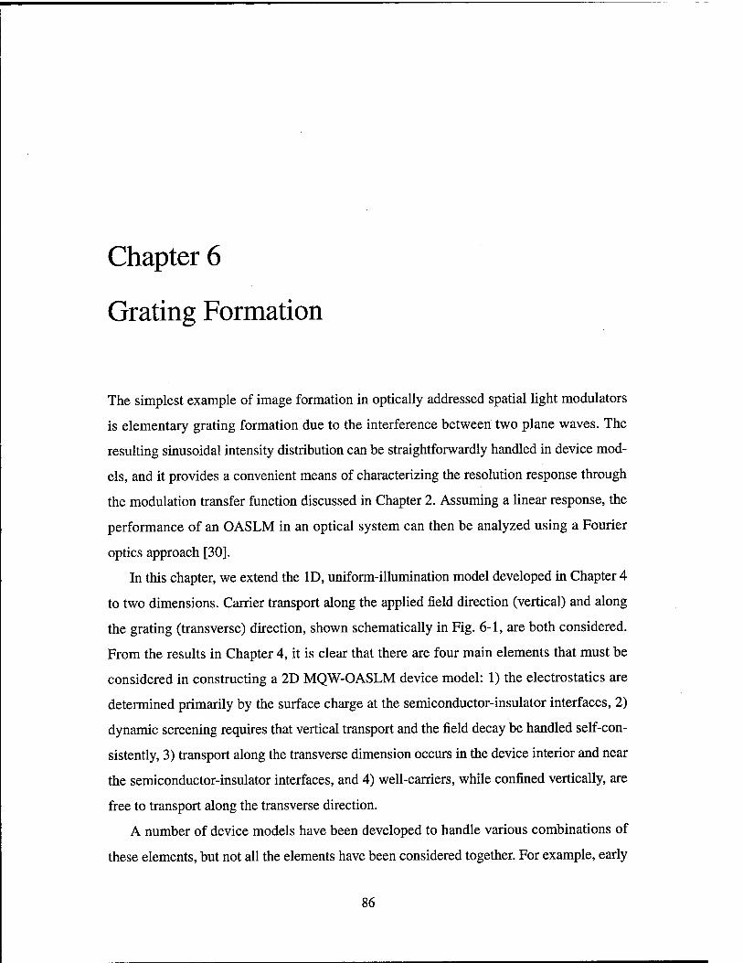
Chapter 6
Grating Formation
The simplest example of image formation in optically addressed spatial light modulators
is elementary grating formation due to the interference between two plane waves. The
resulting sinusoidal intensity distribution can be straightforwardly handled in device mod-
els, and it provides a convenient means of characterizing the resolution response through
the modulation transfer function discussed in Chapter 2. Assuming a linear response, the
performance of an OASLM in an optical system can then be analyzed using a Fourier
optics approach [30].
In this chapter, we extend the ID, uniform-illumination model developed in Chapter 4
to two dimensions. Carrier transport along the applied field direction (vertical) and along
the grating (transverse) direction, shown schematically in Fig. 6-1, are both considered.
From the results in Chapter 4, it is clear that there are four main elements that must be
considered in constructing a 2D MQW-OASLM device model: 1) the electrostatics are
determined primarily by the surface charge at the semiconductor-insulator interfaces, 2)
dynamic screening requires that vertical transport and the field decay be handled self-con-
sistently, 3) transport along the transverse dimension occurs in the device interior and near
the semiconductor-insulator interfaces, and 4) well-carriers, while confined vertically, are
free to transport along the transverse direction.
A number of device models have been developed to handle various combinations of
these elements, but not all the elements have been considered together. For example, early
86

87 CHAPTER 6
PROM models considered the role of field fringing due to the space-charge distribution in
determining device resolution [7, 8], and some PROM models considered the effects of
ID and 2D carrier transport [9, 10]. However, the characteristic transport lengths of early
PROM's made with oxide materials placed them in a bulk charge regime. In contrast, the
MQW-OASLM relies on the screening produced by surface, not bulk, charges. More
recent device models have considered ad-hoc surface-charge models along with carrier
transport along the grating direction. Nolte has presented a steady-state model for leaky
insulators which considered interior drift [14]. Wang et dl. have presented a transient
model that included transverse transport in both the interior and surface-charge regions,
but vertical transport was not handled in a self-consistent manner [16]. None of these
models has explicitly considered the role of quantum wells.
In this chapter, we present a 2D device model incorporating all the elements men-
tioned above. Sinusoidal grating formation is simulated using direct numerical solutions to
the transport equations. Simplified numerical and analytical solutions are found when pos-
sible. In particular, a small signal approximation for small intensity modulations is used to
calculate the free-carrier distributions under transverse drift and diffusion. The injection of
free-carriers into the surface-charge regions is then used to determine the transient buildup
and decay of the electric field grating. A brief review of field-fringing effects due to the
surface-charge distribution is also presented. The main results of the small signal model
are verified using full numerical solutions to the transport equations. Finally, the depen-
dence of the grating formation process on the intensity modulation is analyzed.
6.1 Device Model
The device model we use for modeling grating formation is similar to the ID model devel-
oped in Chapter 4, except that here we must consider transport along the applied field
direction and along the transverse direction as shown in Fig. 6-1. As described in
Chapter 4, we consider both free electron and hole transport, as well as the transport of
carriers in the quantum wells. The primary modifications to the ID transport equations

Grating Formation
(a) 'r^C
J^o
ND
We
(b)
£2
ws
<
£1 £2
>V0
x -L-d -L L L+d
-*■ z
Figure 6-1 2D device geometry, (a) Band diagram showing quantum wells and emission/capture processes, (b) 2D device structure showing transport of carriers in the interior and in the surface- charge regions near the semiconductor-insulator interfaces. Both vertical transport (z) and trans- verse transport (x) are considered.
involve adding transverse current terms to the continuity equations for free carriers and for
well carriers. A 2D Poisson equation is also used. The 2D transport equations are summa-
rized below:
dN l^JN n ,R . „ wtu. dt dx
(6-1)
^ = -it+r-^+^^-^+))p dp dt
(6-2)
3Ag dt
= yP(ND-N+)P-yNN+N (6-3)
dn lyj . , , . n (6-4)

89 CHAPTER 6
ft=-lvjp + g(X,z)-£ (6-5)
V-(eW) = -e(Np-NA + p-n + P-N) (6-6)
The continuity equations for free carriers now contain 2D current densities given by
jn = e\in(nE + VTVn) (6-7)
jp = e\ip(pE-VTVp) (6-8)
where E is the field. The electron and hole mobilities are taken to be anisotropic to
account for transverse transport parallel to the quantum wells, \\.nx and \ipx, and for vertical
transport along the applied field, \inz and \ipv Anisotropic mobilities are used for two rea-
sons. First, it is expected that the mobilities along the growth direction will be smaller than
the transverse mobilities due to alloy scattering and scattering from the well-barrier
interfaces [77]. Second, in determining the relative contributions of various transport
mechanisms on the screening process, it is convenient to selectively suppress some mech-
anisms by setting the appropriate transverse mobility to zero in the simulation.
The transverse current terms in the well-carrier continuity equations are given in
Chapter 3 as
jN = e^NE^V^ (6-9)
Jp = ^p{PEx-VTd£] (6-10)
The boundary conditions for the free-carrier current densities and the applied voltage
are the same as those used for the ID model in Chapter 4. The generation term is given for
an elementary grating formed by beams incident from the left in Fig. 6-1 as
g(x,z) = -r^il+mcosKx) e~a{z + L) (6-11) nv

Grating Formation 90
oA(x) OR(X)
«f-
-► z
X
Figure 6-2 Illustration of surface-charge grating formation under sinusoidal illumination condi- tions indicated by the light and dark fringes. This intensity pattern could be produced, for example, by the interference between two plane waves. Electrons and holes are injected into the surface- charge regions and accumulate. The net surface charge at the interfaces is given by aA and CTg.
where m is the intensity modulation, and K=2it/h is the spatial frequency with A the grat-
ing spacing. Periodic boundary conditions are used along the grating direction. When full
numerical solutions to the above system are required, they are computed using the tech-
niques described in Appendix A.
6.2 Small Signal Injection Model
In Chapter 4 a picture of ID device operation was presented that described the screening
of the applied voltage as occurring through the accumulation of carriers in traps near the
semiconductor-insulator interfaces. As illustrated in Fig. 6-2, interior carriers inject and
accumulate in a thin surface-charge region near the interfaces. Since the screening rate due
to this buildup is proportional to the intensity, a sinusoidal illumination pattern produces a
variation in the screening rate across the device. During the initial stages of grating forma-
tion, this creates a spatially modulated surface charge that mimics the intensity pattern.
The grating formation is transient, however, since the applied voltage eventually becomes
fully screened across the entire device.
In this section, a number of issues related to the transient buildup and decay of the
screening charge are examined. First, various aspects of the electrostatic solutions for
sinusoidal surface-charge patterns are examined, including the resolution limitation

91 CHAPTER 6
imposed by field fringing. The free-carrier distributions are then calculated in a small sig-
nal model developed for intensity modulations much less than unity. In this approxima-
tion, the carrier continuity equations are linearized in the intensity modulation for easier
analysis. This model is used to determine the effects of transverse transport on the carrier
modulations. Finally, the transient buildup and decay of the electric field grating produced
by the modulated surface charge is calculated in both the short and long vertical drift
length regimes.
6.2.1 Electrostatics
Assuming the grating response is linear in the intensity modulation, the surface charge at
each interface can be expanded as
(0) -(i) v CTA = cr ' + mcA cosKx
m -<» r (6"12)
oB = -a + mcB cos AX
where aA and aB refer to the left and right interfaces in Fig. 6-2, respectively, and all the
components are real. Charge neutrality has been used to write the zeroth-order compo-
nents. The corresponding expansions for the field components are
Ez(x,z) = Ez0) + mEz
{X\z) cos Kx (6-13)
Ex(x, z) = -mEx (z)sinKx (6-14)
where Ez , Ez , Ex are all real. The "A" on top of the first-order components indicates
that the linear-in-m dependence has already been taken into account. The field compo-
nents can be calculated in terms of the surface charge components by direct solution of the
Poisson equation. The resulting field distributions display fringing effects at small grating
spacings. These effects have been considered in detail before and produce a lower limit on
the device resolution of approximately twice the device length [7, 8]. There are two limit-
ing cases of interest: oB = -oA and aB = 0.

Grating Formation 92
The optimum field pattern for efficient electro-optic modulation is produced when
aB = -oA. The field components in the interior are then
E ,(i) AO) ,B2yanh(^L)-
eJtanhC^). -lcosh(Kz)
cosh(KL) (6-15)
Z? = ».(!>
-1 L
■^tanh (ÜTL)T1 sinh(ffz) 1 ' ' '"" cosh(^L) .EjJtanhC^).
,(D For long grating spacings such that K ~ 0, Ez is constant throughout the interior while
E^-0. This optimizes the electro-optic response and suppresses transverse drift. At
smaller grating spacings, field fringing becomes significant, causing Ez to decay into the
device center and Ex to increase near the interfaces. This reduces the electro-optic effect
and increases transverse drift near the interfaces. As can be determined from Eq. (6-15),
the resolution limit imposed by field fringing is approximately twice the device length for
typical dielectric permittivities.
In some devices, one of the interfaces may have a particularly weak trap density that
allows the carrier modulation and the surface charge to become completely washed out.
This could happen, for example, if the carrier lifetime in one of the interface regions is not
reduced through low-temperature growth or other techniques. In this situation, the grating
component of one of the surface-charge patterns, say aB, vanishes. In this situation, the
field components are given by
,(i) ,(D,
Z 2El1
x 2e, I
1 +
1 +
tmh(KL) -i-l
tmh(Kd)
^tmh(KLJ
v v tmh(Kd)
cosh(Kz) cosh(KL)
sinh(Kz) cosh (KL)
1 +
1 +
fe^ coth(KL) tanh(Kd)
coth(KL)
4 sinh(gz)] sinn
tanh(Kd) cosh(Kz) I sin] ih(KL))
(6-16)
For this case, both the x and z components contain terms that are symmetric and anti-
symmetric in z. For E{1)
, the smh(Kz) term effectively plays no role in the electro-optic
phase modulation since the net phase change, after integrating over the device length,

93 CHAPTER 6
vanishes. The cosh(Kz) term, however will contribute, producing a net phase change that
is one-half that of the aB = -cA case. Thus, losing the surface-charge modulation at one
interface cuts the phase modulation in half for the same amount of surface charge.
6.2.2 Carrier Distributions
To determine the free-carrier distributions, all variables are expanded in the following
form, using the free-electron concentration as an example: n = n0(z) + mhl(z)cosKx.
Using the quasi-steady state approximation and plugging these Fourier expansions into the
free- and well-carrier continuity equations, effective continuity equations for the first
Fourier components of the free-carrier densities can be found. The zeroth-order compo-
nents of the free-carrier densities are given in Chapter 4. The free-carrier distributions are
best characterized in terms of the various transport lengths, i.e. the vertical and transverse
drift and diffusion lengths. For computing the first-order components, we consider here
two different cases: transport lengths much shorter than the device length, and transport
lengths much longer than the device length.
Short Transport Lengths
For transport lengths much shorter than the device length, transverse drift and diffusion
can be neglected since field fringing dominates the device performance at small grating
spacings before transverse transport becomes significant. In this regime, the first-order
components of the free-carrier densities are the same as the zeroth-order densities,
Eq. (4-14). For small absorption, the interior densities are uniform and given by
"i = So^Rn anc* Pi = 8o^Rp where TWnand xR are the effective recombination times
for electrons and holes, respectively.
Since transverse transport is negligible, the surface-charge rate equations for the first-
order components are also similar to the rate equations for the zeroth-order components.
For the electron surface-charge region, for example, the rate equation is given by

Grating Formation 94
do (1) B ,(D)
dt JPZ + ;(1) Jnz (6-17)
*0
Long Transport Lengths
For transport lengths much longer than the device length, it is necessary to consider trans-
verse drift and diffusion when calculating the free-carrier densities. Transverse diffusion
drives carriers from regions of high concentration to regions of low concentration, thereby
reducing the modulation of the carrier densities. Due to the phase of Ex from Eq. (6-15),
transverse drift also drives carriers from regions of high to regions of low concentration.
Including transverse transport in the continuity equations complicates the quasi-steady
state equations for the first-order free-carrier densities. For example, the first-order com-
ponent of the free-electron density is given by the solution to
d n, dh -4-^w + (i+n„Avn"i <6-18>
dz äz
- - - eJMr - ~ dK£|1}) = 8olRn-V'nx*nEx Kn0 + \inzXn j£
where \inx is the effective transverse mobility due to transport above the barriers and in
the wells. The vertical diffusion length, LD, the vertical drift length LE, and the effective
carrier lifetime, xn, are the same as those used in Chapter 4. The solution of this equation
requires the zeroth-order component of the free-electron density as well as the first-order
field components.
The effective transverse mobility is given in terms of the well-electron and free-
electron mobilities. Since Eq. (6-18) is derived for the long vertical drift length regime, in
this section we therefore only consider devices with good carrier escape rates and long
carrier lifetimes. Under these conditions ßNtN»l, and \inx is given by

95 CHAPTER 6
This is the weighted sum of the free-carrier transverse mobility and the well-confined
mobility in which the weighting factors are given by the relative time spent in the conduc-
tion band above the barriers and in the well, respectively. Transport in the wells thus
increases the anisotropic nature of carrier transport, and for moderate escape rates and fast
carrier capture times, the effective transverse mobility is determined by the well mobility.
The buildup of the surface charge is calculated from the trapping of free carriers by
traps in the surface-charge regions. As discussed in Chapter 4, the buildup of the surface
charge in the electron surface-charge region is given by
daB rLdN+D rLn
-=r- = e -^r—dz ~ -e —dz (6-20) dt JZo dt JZo^
for long vertical drift lengths.
Using the electron continuity equation and the current boundary conditions, Eq. (6-20)
can be rewritten as
ns 9 fL -T, = Jnzl "ä^J JnA (6"21>
XM ,zo OXJz0
where ns = | n(z)dz is the net surface density of electrons, and jnz = e\inznEz is the
injecting current from the interior, neglecting diffusion. This current is evaluated at the
interior edge of the surface-charge region, z0 in Fig. 4-1, and only uses the relaxation term
of the electron density. The transverse current in the surface-charge region is given by jnx.
To proceed, Ex is assumed to be independent of z in the surface-charge region. This
can be verified by considering that VxZ? = 0, and has also been verified in direct numeri-
cal calculations. The resulting free-electron surface densities in the surface-charge region
are given in terms of the Fourier cosine components of ns andynz as
(0) .(0) n = l s Jnz ?Rn (6-22)

Grating Formation 96
*..(l)~s ~s ~sv (0)^,(1) (1) _ Jnz xRn ~ \inxZnKns Ex
n„ = * , ~s ~s 1+tiXVrK2 (6-23)
*0
where \Lnx is the effective transverse mobility in the surface-charge region.
Equations (6-22) and (6-23) describe the development of the electron distribution in
the surface-charge region as arising from two sources. The first source is the injection of
electrons from the interior into the surface-charge region. The second source is the trans-
verse drift and diffusion of electrons within the surface-charge region. A similar analysis
for hole transport at the opposite interface produces analogous results. Equations (6-22)
and (6-23) can be used in Eq. (6-20) to compute the surface charge.
6.2.3 Grating Formation
The time dependence of the first-order vertical field component, E^\ can now be com-
puted by considering the buildup of the trapped surface charge. The solutions for the
zeroth-order component, E^0), are the same as in Chapter 4. We consider here the long
grating spacing limit (A » L) in which all transverse transport is negligible and in which
all field components are independent of z. The rate equations for the surface charge com-
ponents then contain only injection from the interior carriers. For the long transport length
case, the transverse drift and diffusion terms in the continuity equations for interior carri-
ers, Eq. (6-18), are neglected. This simplifies the analysis and allows the calculation of the
basic time dependence of grating formation. The effect of transverse transport at smaller
grating spacings will be examined in the following chapter. We assume that the electron
and hole response is symmetric so that d^ = -a^ . As discussed in Chapter 4, it can be
shown that this approximation is valid for very short vertical drift lengths and very long
vertical drift lengths. However, this approximation is inaccurate for intermediate cases, but
it does simplify the analysis.

97 CHAPTER 6
Short Vertical Drift Lengths
For short vertical drift lengths, the complete time dependence of the first-order field com-
ponent can be solved analytically. Expanding the first-order current in the surface-charge
rate equation, Eq. (6-17), and using Eq. (6-15) to write the surface charge in terms of the
field, the rate equation for the first-order field component is
-^- + -£- = ~i- (6-24) at x0 x0
where x0 is the screening time from Eq. (4-22). The buildup of E^ is driven by the
zeroth-order component on the right-hand-side and damped by itself on the left-hand-side.
Using the zeroth-order result, Eq. (4-23), and the initial conditions £(°) = -EQ and
E^l) = 0, the solution to Eq. (6-24) is
M" = Ejgy* (6-25)
For times short compared to the screening time, x0. the grating builds up in a linear fashion
from the injection of the modulated carriers by the zeroth-order field component. The
growth slows, however, as the field becomes screened in the more illuminated regions. At
time T0 the grating peaks at a value of e~ Eo
becomes screened even in the darker regions.
time T0 the grating peaks at a value of e Eo and then decays slowly as the interior field
Long Vertical Drift Lengths
For long vertical drift lengths, the complete buildup and decay of the first-order compo-
nent cannot be solved analytically. After expanding the injection current components, the
rate equation for the first-order field component is
^-^XoK^^) (6-26)

Grating Formation 98
ui
1.0
0.8 -
0.6
O N <UJ 0.4
0.2
—I—I—I—I—|—I—I—i—I—|—i—r—l i | i i ■■1 1 1 1 1 1 1
400
/ 1 40 - 4
/ • / / \ - // \ // I //
// ' ~ - *- - _ // - *"* \ — - „^ ""
-■». / s I ** ■ ^
jT s \ / s V ~ / ' * / /' \ v /',,,. 1 I I I 1 1 1 1 Vi 1 1 !_Ü
0.2 0.4 0.6 0.8 Normalized Time
1.0
Figure 6-3 Buildup and decay of the first-order field component during grating formation for the indicated values of Lß/L.
where %0 is given by Eq. (4-19). From Eqs. (4-14) and (6-18), the electron Fourier compo-
nents are themselves functions of the field components . The resulting nonlinear system is
solved numerically with the following initial conditions: £(°) = -E0 and E^ = 0. The
solutions can be characterized in terms of the absorption coefficient, a, and the initial
value of the drift length, LE, at the start of the screening process.
Solutions to Eq. (6-26) are shown in Fig. 6-3 for various values of the initial vertical
drift length at a = 2.0x104 cm"1. To compare time scales, E0 is held constant, and the ver-
tical mobility-lifetime product is varied to obtain different vertical drift lengths. As dem-
onstrated by the LE/L =400 curve in Fig. 6-3, for long initial vertical drift lengths the
first-order component builds up linearly in time in a manner similar to the zeroth-order
component, but then decays rapidly as the bias voltage becomes fully screened. For
LE/L -> °°, the peak value of E^ approaches E0.
For smaller values of the initial drift length, the initial buildup of E[X) slows. In addi-
tion, the peak value decreases, and for very short drift lengths, it approaches e~ EQ as pre-
viously discussed. The fall time also increases dramatically as shown in Fig. 6-3 for the
LE/L=A curve. In general, longer vertical drift lengths produce a faster rise, a larger peak
grating amplitude, and a shorter fall time, all of which are desirable for optimum device
performance.

99 CHAPTER 6
6.3 Numerical Results
In this section, we examine some of the details of the screening process using direct
numerical solution of the transport equations and assess the validity of the main approxi-
mations used in the development of the small signal injection model described previously.
Three main approximations were made in the development of the small signal injection
model: 1) the space charge is dominated by surface charge, 2) the response is linearly pro-
portional to m, and 3) the grating spacing was restricted to values much greater than the
device length. To investigate the validity of these approximations, grating formation was
simulated in a device with the parameters listed in Table 4-1 and the following transport
parameters: equal electron and hole parameters with effective vertical mobilities of
180 cm2/V-s, effective transverse mobilities of 2000 cm2/V-s, effective interior free-car-
rier lifetimes of 1 ns, and effective surface-carrier lifetimes of 10 ps. These effective
parameters are appropriate for electron transport in AlGaAs using the shallow trap model.
Equal electron and hole parameters were used to simplify the analysis of the results. These
parameters place the device in the long transport length regime which is optimal for speed
and peak grating amplitude. To compare the results with the small signal model, the first-
order Fourier component of the vertical field is computed numerically and then normal-
ized by the intensity modulation to give Ez .
6.3.1 Field Uniformity
In Fig. 6-4 the vertical profile of Ez along the device length for m = 1.0 is shown at the
peak of the grating amplitude and for long grating spacing (A » L). The profile is quite
uniform, with most of the variation occurring in the surface-charge regions near the inter-
faces as was the case for the zeroth-order component in Figure 4-6. This also supports the
surface-charge model of field screening.
The field profile in Figure 6-4 was computed for long grating spacings where trans-
verse transport is not significant. The surface-charge components at both interfaces were
found to have approximately the same modulation. However, at smaller grating spacings,
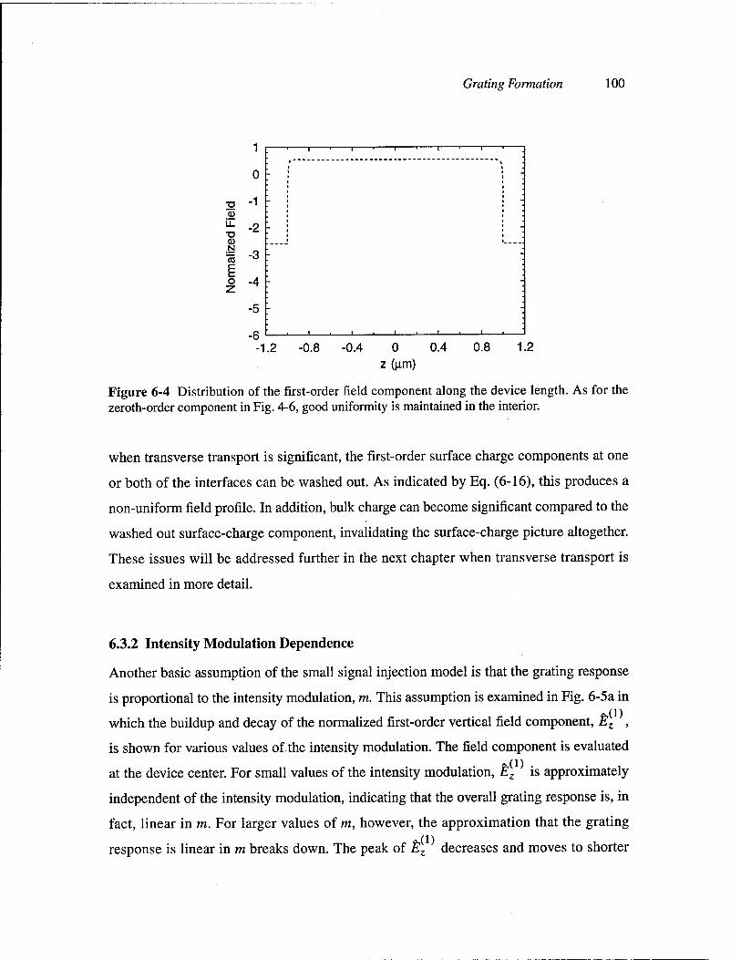
Grating Formation 100
0
■D -1 CD
LL -? ■n m N m -3 F o -4 ü
-5
-1.2 -0.8 -0.4 0 0.4 z((im)
0.8 1.2
Figure 6-4 Distribution of the first-order field component along the device length. As for the zeroth-order component in Fig. 4-6, good uniformity is maintained in the interior.
when transverse transport is significant, the first-order surface charge components at one
or both of the interfaces can be washed out. As indicated by Eq. (6-16), this produces a
non-uniform field profile. In addition, bulk charge can become significant compared to the
washed out surface-charge component, invalidating the surface-charge picture altogether.
These issues will be addressed further in the next chapter when transverse transport is
examined in more detail.
6.3.2 Intensity Modulation Dependence
Another basic assumption of the small signal injection model is that the grating response
is proportional to the intensity modulation, m. This assumption is examined in Fig. 6-5a in
which the buildup and decay of the normalized first-order vertical field component, Ez ,
is shown for various values of the intensity modulation. The field component is evaluated
at the device center. For small values of the intensity modulation, Ez is approximately
independent of the intensity modulation, indicating that the overall grating response is, in
fact, linear in m. For larger values of m, however, the approximation that the grating
response is linear in m breaks down. The peak of Ez decreases and moves to shorter

101 CHAPTER 6
HI
(a) ~
(b)
<LU
-0.2 20
0.01 — -0.1 ---0.2 0.4 0.6 ---0.8 —-1.0
■ ■ ■ i
40 60 Time (us)
80 100
CD E g is o
0.8
0.6
ä 0.4 O 0) £ 0.2 o
LU
I i r i
/ vv* 0.01
■ / VN- 0.1 ---0.2 -
/ v \ "v — -0.4 / Y- * N"~ 0.6 .
- / v. \ *-s- ---0.8 - / v ■ ' ^■^ 1.0 / \\ '• \
:/ \\ '■■• \
'"•-^^ _
7 r '■• x \ .
7 h ^ *'" \ „
f \N \ '•• -..
20 40 60 Time ((is)
80 100
Figure 6-5 Dependence of the grating response on the intensity modulation, (a) Vertical first-order field component for the indicated values of the intensity modulation, (b) Corresponding effective grating modulation, m,Q, defined in Eq. 6-30.
times, and the fall-time increases dramatically. The latter effect is due to the large differ-
ence in screening times in the light and dark fringes at large m. The small signal injection
model, therefore, really is a small signal model, limited to values of m less than about 0.2.
As discussed in Chapter 2, the linearity of the overall diffraction process is character-
ized by the linearity of the transmission of the first-order diffracted beam. The transmis-
sion of the first-order diffracted beam is determined by the dielectric grating produced by

Grating Formation 102
the first-order vertical field component and the electro-optic effect which, in this case, is
the QCSE. The QCSE produces changes in both the index of refraction and the absorption
coefficient. These changes are, to lowest order, quadratic in the vertical field component 1 o 2 2XC 3 2
and can be written as An = --n0slEz and Ace = -^-n0s2Ez, where n0 is the unmodu-
lated index of refraction, X0 is the free-space wavelength, and sj and s2 are the quadratic
electro-optic coefficients [46]. The complex index grating with grating vector K produced
by the field expansion from Eq. (6-13) will then be An' cos Kx, where
An' = -\nl{sx + is2)G{z) (6-27)
and G(z) = 2m E^E^. As discussed in Chapter 2, the readout of such a grating pro-
duces Raman-Nath diffraction with the small signal transmission into the first diffracted
order given by
7-!—«| (6-28)
where the phase shift, 8, is given by
8 = -^-(,1 + /,2)fLG(z)Jz (6-29)
AOCOS0 l z J_L
The dependence of the transmission on the grating formation process is thus contained in
G(z).
To characterize the dielectric grating response for various intensity modulations and
grating spacings, we normalize the integral of G(z) and define an effective grating modula-
tion function, mG, as
J. G(z)dz mQ = Lk _ (6-30)
TULEQ
The normalization value used here is the maximum value of the integral of G(z) calculated
from the small signal injection model for long vertical drift lengths.

103 CHAPTER 6
The plots of YUQ corresponding to the same values of the intensity modulation used in
Fig. 6-5a are shown in Fig. 6-5b. The responses for all values of the intensity modulation
are nearly identical during the initial formation of the grating up to the peak amplitude.
The peak values for all intensity modulations are approximately unity, in good agreement
with the results from the small signal injection model. The decay of mG, however, depends
strongly on the intensity modulation, and very asymmetric rise and fall times are produced
for large values of m.
These results indicate that the transmission linearity of the first-order diffracted beam
should be quite good during the initial stages of grating formation up to the grating peak.
Linearity during decay, however, appears very poor. In an application such as an optical
correlator where linearity is important, it might therefore be necessary to read out the grat-
ing only during the initial stages of grating formation.
6.3.3 Transverse Transport
The last major approximation used in the development of the small signal injection model
is the restriction to long grating spacings. As the grating spacing is reduced, transverse
transport increases because the transverse diffusion gradient and the transverse field com-
ponent increase. This is illustrated in Fig. 6-6 in which the peak amplitude of Ez (z=0)
for m = 0.1 is plotted versus grating spacing for two cases: the geometric case in which
transverse transport is suppressed, and the nominal case in which transverse transport is
included. The artificial suppression of transverse drift and diffusion in the simulation
allows for a convenient analysis of the relative contributions of various transport mecha-
nisms to the screening process. Both curves in Fig. 6-6 are normalized by the long grating
spacing value. While the resolution in the geometric case falls off at around twice the
device length, the resolution in the nominal case falls off at a much longer grating spacing.
Using a 50% decrease in the amplitude of Ez from the long grating spacing value as a
resolution criterion, the geometric resolution limit is 3.7 |im while the nominal resolution
limit is only 22 |im. As we will see in the following chapter, this precipitous roll-off is due
primarily to transverse drift.

Grating Formation 104
1.2
1
0.8
-ri i i n| 1 1—■ i i i i i| 1 1—r-T-T-rtT] i i
p t / t /
1 /
<LU ; I
N
E o
0.6
0.4
0.2
'-
i I i t
i / i I
i /
i / f /
i / i /
i /
-
0
-0.2 0
t ^s ■
1 1 10 100 10 Grating Spacing (|im)
Figure 6-6 Geometric (dotted) and nominal (solid) resolution curves. The nominal resolution curve rolls off at longer grating spacings due to transverse transport. The geometric resolution curve rolls off due to field fringing.
6.4 Summary
In the previous chapter it was found that the screening rate under uniform illumination was
optimized for vertical drift lengths much longer than the device length. In this chapter, a
small signal analysis of grating formation under sinusoidal illumination showed that long
vertical drift lengths optimize not only the initial rise time of the grating, but also the fall
time and the peak grating amplitude. These results, however, were limited to long grating
spacings in which transverse transport was negligible. A cursory examination of the
impact of transverse transport on resolution indicated that, in the long transport length
regime, a severe degradation of resolution can occur. It remains to be seen if all three per-
formance criteria- speed, peak grating amplitude, and resolution- can be simultaneously
optimized through appropriate device design. A detailed analysis of various techniques to
optimize overall device performance will be presented in the next chapter.
In addition to speed, peak grating amplitude, and resolution another important crite-
rion for OASLM performance is linearity, characterized in this chapter by the dependence

105 CHAPTER 6
of the dielectric grating on the intensity modulation. Full numerical solutions to the trans-
port equations established that the complex phase modulation created by screening and
subsequent QCSE modulation is in fact linear in the intensity modulation, at least for short
times. This implies that the transmission of the first-order diffracted beam is also linear for
small phase modulations. For long times, however, the grating response was found to be
very nonlinear, especially at large intensity modulations. In some applications, this may
constrain the readout of the grating to the initial stages of grating formation in order to
assure a linear response.

Chapter 7
Resolution Performance
As discussed in the previous chapter, for typical MQW-OASLM device designs the resolu-
tion performance is limited by the transverse transport of electrons and holes. Transverse
transport washes out the modulation in the carrier densities and causes the modulation
transfer function to roll off at grating spacings much longer than the geometric, field-
fringing limit. Some of the first experimentally demonstrated devices displayed this type
of behavior, with resolutions worse than 30 u.m. Recently, there have been several experi-
mental efforts to optimize various aspects of device performance including resolution,
speed, and diffraction efficiency. Diffraction efficiency is determined primarily by the
strength of the quantum confined Stark effect and can be increased through different well-
barrier designs [78] and the use of asymmetric Fabry-Perot etalon structures [79]. The
optimization of speed and the optimization of resolution are in fact linked and have been
pursued along two different approaches. One approach has concentrated on optimizing
resolution performance by using semi-insulating, short lifetime quantum-well material in
the interior region to suppress interior transport [80]. While this technique appears suc-
cessful in improving resolution performance, devices fabricated with this design suffer a
relatively slow frame rate. Another approach has attempted to optimize speed by using an
intrinsic interior region to reduce the carrier transit times [62]. Initial results indicate that
this technique can improve the frame rate while still maintaining good resolution as long
as the semiconductor-insulator interface region is made strongly semi-insulating. In this
106
107 CHAPTER 7
chapter we investigate the trade-offs and limitations involved in simultaneously optimiz-
ing both the speed and resolution performance
To calculate the resolution performance, we use the device model described in the pre-
vious chapter. The roles of drift and diffusion in both the interior and surface-charge
regions in determining the resolution performance are examined. The results of full
numerical solutions, as well as analytical estimates of the transport-limited resolution, are
presented. A brief discussion of nonlinear transport effects specific to semiconductor and
quantum-well materials is also given, focusing on the relevance to resolution performance.
An example of device optimization in which experimentally accessible device parameters
are modified to optimize both speed and resolution performance is also presented.
7.1 Transverse Transport
Transverse transport along the grating direction washes out the carrier modulation,
reduces the grating amplitude, and pushes the resolution limit to longer grating spacings.
This is exacerbated by the presence of quantum wells which allow the transport of con-
fined, as well as free, carriers. In the small signal injection model developed in the previ-
ous chapter, the device was modeled as consisting of an interior region and two surface-
charge regions near the semiconductor-insulator interfaces. As a carrier in the interior
drifts towards one of the interfaces, it also drifts and diffuses along the grating vector,
washing out the carrier modulation. Once injected into the surface-charge region, the car-
rier undergoes further drift and diffusion along the interface before being trapped, which
also reduces the carrier modulation. The carrier densities in the interior and in the surface-
charge regions can be estimated from Eqs. (4-14), (6-18), (6-22), and (6-23). The calcula-
tion of the full time dependence of the resulting screening behavior, however, requires
direct numerical solution of the original transport equations. To isolate the effects of drift
and diffusion in the two device regions, each transport process can be selectively activated
in the simulation. Simulations were performed using the device parameters in Table 4-1,
using equal electron and hole parameters. The mobilities, well escape rates, and carrier

Resolution Performance 108
lifetimes were adjusted to examine transverse transport for various vertical and transverse
transport lengths. The grating spacing at which the peak value of Ez {z = 0) was reduced
by 50% from the value at long grating spacings was used as a resolution criterion to com-
pare the various transport effects. As mentioned above, we are primarily interested in the
long vertical drift length regime in which the speed response is optimized.
7.1.1 Interior Transport
The initial buildup of screening charge due to the injection of interior electrons into the
surface-charge region is given by Eqs. (6-20) and (6-21). In the long vertical drift length
regime, the surface-charge rate equation is
dt = eKzhlE (7-1)
Using the zeroth-order electron component from Eq. (4-14) in the limit of LE/L»\, the
surface-charge rate equation can be approximated as
IF = eg% x 1/oc aL>>1 (7-2) I 2L aL«l
where the upper factor is for high absorption and the lower factor is for low absorption.
The initial buildup of the surface-charge grating component is thus proportional to the
effective electron modulation, hx/nQ, at the interior edge of the surface-charge region.
Transverse diffusion acts to transport carriers from lighter to darker regions. For long
vertical drift lengths, the effective electron modulation at low absorption (aL « 1) is cal-
culated from Eq. (6-18) as
h=lJf\K2L2D (7-3)
where the transverse diffusion length in the interior is given in terms of the effective trans-
verse mobility and lifetime as LD = tl\Lnx:znVT. For high absorption (aL » 1), the

109 CHAPTER 7
effective electron modulation depends on whether the electrons are drawn to the front or
the back of the device relative to the incident beam:
1± n0
1 (2L\ T.i T 2 X~{L;)KLD> back
W ' (7-4)
1 front
where the upper result is for electrons drawn to the back and the lower result is for elec-
trons drawn to the front. For low absorption, the response is the same whether the elec-
trons are drawn to the back or to the front. The L/LE factor in Eq. (7-3) can be interpreted
as the mean transit time, given by L/\ilnzE0, divided by the interior electron lifetime, xn.
The high absorption case can be interpreted similarly. For high absorption, back-drifting
carriers are generated only at the front of the device and must transport a distance of 2L to
the back. For carriers drawn to the front, there is essentially no transport in the interior at
all.
The results in Eqs. (7-3) and (7-4) indicate that improving vertical transport can sup-
press transverse diffusion. The subsequent effect on the screening of the electric field is
shown in Fig. 7-1 in which the simulated resolution limit imposed by transverse interior
diffusion is plotted versus the effective vertical mobility-lifetime of the free carriers.
Results for two values of the effective transverse mobility-lifetime product are shown. The
best resolution that can be achieved is given by the geometric limit due to field fringing.
For both values of the transverse mobility-lifetime product, the resolution performance
improves dramatically as the vertical transport behavior improves. For a transverse mobil-
ity-lifetime product of l.OxlO"6 cm2/V, the effects of transverse diffusion are almost fully
suppressed below the geometric resolution limit at a vertical mobility-lifetime product of
1.0xl(r6cm2/V.
Due to the phase of Ex, given by Eqs. (6-14) and (6-15), transverse drift also drives
carriers from light to dark regions, washing out the carrier modulation. Although the effect
of transverse drift is difficult to consider analytically due the z dependence and the
dynamic buildup of Ex , a simplified model in which Ez = -E0 and Ex ) = E0sinhKL

Resolution Performance 110
1000
E 3 100 r c o
o w 05 -in L DC 10 "
-1 1 1 IT
ZJn =10-4(cm2/V)
pnxxn =10-6(cm2/V)
Geometrie Limit
10- 10-7
KX (cm2/V) 10"
Figure 7-1 Resolution limit imposed by interior diffusion versus the effective vertical mobility- lifetime product of the free carriers. Results for two values of the effective transverse mobility- lifetime products of the free carriers are shown. The geometric limit due to field fringing is also shown.
can be used to indicate the effect of vertical drift. Using these field values in Eq. (6-18),
the effective electron modulation for low absorption is found to be
«1
«n (r> (7-5)
while the result for high absorption is
IK back
\aLpJ
(7-6)
KLE front
s(l) where LE = )inxTnEx is the transverse drift length in the interior due to fcx . As was
the case for interior diffusion, the effect of transverse drift is suppressed by the ratio of the
vertical transit time divided by the effective carrier lifetime. This is demonstrated in
Fig. 7-2 where the simulated resolution limit imposed by transverse interior drift is plotted
versus the effective vertical mobility-lifetime product for two values of the effective

Ill CHAPTER 7
1000
E 100 3. c o J5 o
GC
I I I
jlnx?n =10-4(cm2/V)
P ? =10"6(cm2/V)
Geometric Limit
10" 10-7
aX (cm2/V) 10"
Figure 7-2 Resolution limit imposed by interior drift versus the effective vertical mobility- lifetime product of the free carriers. Results are shown for the indicated effective transverse mobility-lifetime products of the free carriers.
transverse mobility-lifetime product. As in the diffusion case, the resolution performance
improves as the effective vertical mobility-lifetime product increases. For the applied volt-
age used to generate Figs. 7-1 and 7-2, 20 V, transverse drift produces a resolution limit
that is a factor of four worse than that produced by transverse diffusion.
The results above indicate that to suppress transverse transport in the interior, it is nec-
essary to reduce the anisotropy between vertical transport and transverse transport. In
practice, this can best be achieved by increasing the escape rate of well carriers. This can
be seen by considering that transverse drift and diffusion can be characterized by an effec-
tive drift length {L/LE)LEx, where LEx = jI^T^, and Ex = EXX) for drift and
Ex = KVT for diffusion. For weak absorption, for example, the effective free-electron
modulation is given in terms of the transit time, ttr = L/\ilnzE0, as
r = i-^(WA) (7-7)
This result indicates that the actual transverse transport length is determined by the transit
time and not by the carrier lifetime. The transit time can be reduced by improving the well
escape rates through the use of wells with lower barriers. This technique increases the
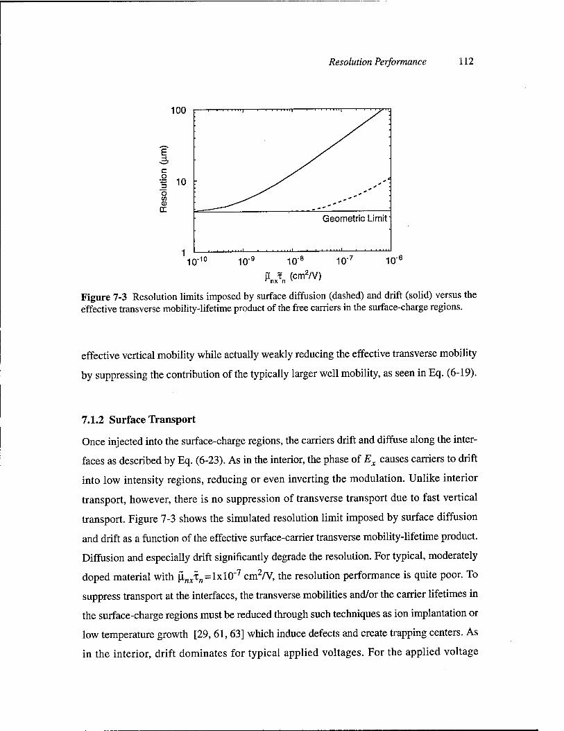
Resolution Performance 112
100
E 3. c o •§ 10 ö w 0
Geometrie Limit'
10 -10 io- 10"B
p x (cm2/V) 10 ,-7 10-
Figure 7-3 Resolution limits imposed by surface diffusion (dashed) and drift (solid) versus the effective transverse mobility-lifetime product of the free carriers in the surface-charge regions.
effective vertical mobility while actually weakly reducing the effective transverse mobility
by suppressing the contribution of the typically larger well mobility, as seen in Eq. (6-19).
7.1.2 Surface Transport
Once injected into the surface-charge regions, the carriers drift and diffuse along the inter-
faces as described by Eq. (6-23). As in the interior, the phase of Ex causes carriers to drift
into low intensity regions, reducing or even inverting the modulation. Unlike interior
transport, however, there is no suppression of transverse transport due to fast vertical
transport. Figure 7-3 shows the simulated resolution limit imposed by surface diffusion
and drift as a function of the effective surface-carrier transverse mobility-lifetime product.
Diffusion and especially drift significantly degrade the resolution. For typical, moderately
doped material with ji^T^lxlO"7 cm2/V, the resolution performance is quite poor. To
suppress transport at the interfaces, the transverse mobilities and/or the carrier lifetimes in
the surface-charge regions must be reduced through such techniques as ion implantation or
low temperature growth [29, 61, 63] which induce defects and create trapping centers. As
in the interior, drift dominates for typical applied voltages. For the applied voltage
113 CHAPTER 7
considered here, 20 V, the resolution limit imposed by carrier drift is over an order of mag-
nitude larger than the resolution limit imposed by diffusion. The drift-limited response
also degrades at higher applied voltages due to the increased transverse field.
Another important parameter to consider in addition to transverse mobility and carrier
lifetime, when attempting to suppress transverse transport at the interfaces, is the width,
ws, of the high-density trap regions near the interfaces. In our analysis so far, we have
taken this width to be wide enough, 50 nm, to accommodate the accumulated carriers. If
the width of this region is made too small, then carriers will undergo transport along the
interfaces with lifetimes given by the smaller, interior trap densities. These relatively long
lifetimes could lead to significant transverse transport and degrade the resolution.
7.1.3 Resolution Estimates
An estimate of the resolution limits imposed by various transport mechanisms can be
obtained by finding the grating spacing, Ares, at which the expressions for the carrier mod-
ulations at the start of the screening process, Eqs. (7-3), (7-5), and Eq. (6-23), vanish.
These results are summarized in Table 7-1. Since only the initial applied field is used to
estimate the carrier modulations, and the drift estimates are based on a simple field model,
the absolute values predicted by these estimates do not agree completely with the numeri-
cal results which consider the full transient solution. The power law dependencies on the
various transport parameters, however, do agree well with the results in Figs. 7-1, 7-2, and
7-3. For interior transport, the importance of the transport anisotropy is reflected in the
dependence of the resolution limit on the ratio of the effective transverse to effective verti-
cal mobilities. For surface transport, the resolution limits are essentially determined by the
effective transverse mobility-lifetime product.
7.1.4 Intensity Modulation Dependence
The resolution curves shown in Figs. 7-1, 7-2, and 7-3 were all computed using the same
value of the intensity modulation ratio, m = 0.1. The dependence of grating formation on

Resolution Performance 114
Transport Effect Ares
Interior Diffusion OTTT ¥nx VT
Interior Drift iTlLff
Surface Diffusion ^J^nx\VT
Surface Drift ^^nx^nEQL
Table 7-1 Estimated resolution limit, Ares, due to various transport effects. The diffusion estimates are for a constant field, E0. The drift estimates use a simple field model described in the text.
the intensity modulation was considered in the previous chapter, but only at long grating
spacings. For the diffraction process to be truly linear, it is necessary that the grating
amplitude depends linearly on the intensity modulation even at small grating spacings. To
investigate the dependence of the grating amplitude on intensity modulation for various
grating spacings, we computed resolution curves at m = 0.1 and m = 1.0 for a device with
the following parameters: device structure as in Table 4-1, equal electron and hole param-
eters with an effective vertical mobility of 180 cm2/V-s, an effective transverse mobility of
2000 cm2/V-s, an effective interior lifetime of 1 ns, and an effective surface-region life-
time of 10 ps. The simulated resolution curves for £z are shown in Fig. 7-4. The m = 1.0
curve actually shows slightly better resolution behavior (by about 23 %) than the m = 0.1
curve. This implies that the linearity of the grating formation process degrades slightly at
smaller grating spacings.

115 CHAPTER 7
1.2
1
c 0.8 <UJ
I °-6
£ 0.4
0.2
10 100 Grating Spacing (urn)
1000
Figure 7-4 Resolution curve for the peak of the first-order field component. Each curve is normal- ized by its long grating spacing value for comparison. The m = 1.0 case has an approximately 23% better resolution limit than the m = 0.1 case.
7.2 Semiconductor and Quantum-Well Effects
As discussed in the previous chapter, there are a number of unique effects that occur in
semiconductor materials and quantum well structures that can have a large impact on the
vertical transport behavior. Since vertical transport plays an important role in determining
the interior transport behavior, effects such as velocity saturation, resonant absorption, and
field dependent carrier escape from the wells will also impact the resolution performance.
The general impact of each of these effects can be considered within the framework of the
small signal injection model.
The transit time for carrier drift is an important parameter in determining resolution.
Any adverse effect on the transit time will impact the resolution performance. Velocity
saturation and slow escape from quantum wells are two such effects. As discussed in
Chapter 4, velocity saturation produces a field-dependent mobility that degrades at high
fields. The resulting drift velocity saturates at a constant value and limits the transit time.

Resolution Performance 116
This means that increasing the applied voltage will not decrease the transit time and may
actually degrade the resolution performance by increasing transverse drift.
The rate of carrier escape from the quantum wells has the opposite field dependence.
For moderate electric fields, carrier escape from the wells is dominated by thermionic
emission which, for electrons, is not very fast. Small escape rates produce poor effective
vertical mobilities which increase the transit time. As the field is increased, however, the
escape rates generally increase, which improves the vertical mobilities and reduces the
transit time.
Velocity saturation and well-escape have a somewhat indirect, although very signifi-
cant, effect on resolution performance. Resonant absorption, on the other hand, has a very
direct influence on resolution performance. It was shown in Chapter 4 that resonant
absorption essentially produces an effective generation rate for the zeroth-order carrier
components that is reduced by the escape probability of a well-confined carrier. A similar
analysis for the first-order component also produces an effective generation rate, given by
-(1) ( PNX
N Sn = l + $NxN + \iNxNVTK2 1 + ß^ So (7-g)
For this component, the nominal generation rate is reduced by two factors. The first factor
is essentially the escape probability, similar to the factor in the zeroth-order term. The sec-
ond factor describes the reduction in the effective free-carrier generation rate due to photo-
generated well-carriers transporting along the well before escaping. This reduced
photogeneration rate for the first-order carrier components degrades the resolution perfor-
mance by reducing the carrier modulation. This can be avoided by using non-resonant
absorption. Non-resonant absorption prevents this reduction of the first-order photogener-
ation rate, as well as producing a larger zeroth-order generation rate and a larger absorp-
tion coefficient, both of which improve the screening rate.

117 CHAPTER 7
\iN = \inx =4000cm2/Vs \LP = \ipx = 300 cm2/Vs
0
u - ^ 0
u - ^ l+VnzEZ/vsat X+VpzEz/vsat
0 2 Hnz = 4000cnT/Vs
0 2 |Ipz=300cmz/Vs
v"a,= 1.0xl07cm/s V^r=l.0xl07cm/s
Tn = 1 ps Xp = 1 ps
■y2 = 3.2xl0~13cm2/V2 ng = 3.5
XQ = 850 nm
Table 7-2 Carrier mobilities and other parameters used in the optimization example.
7.3 Optimization Example
To examine some of the semiconductor and quantum well effects mentioned previously,
and to demonstrate the effectiveness of adjusting experimentally accessible parameters for
optimization, we performed simulations for two different devices with parameters listed in
Table 4-1 and Table 7-2. Both devices were similar except for differences in the quantum-
well escape rates and carrier lifetimes in the surface-charge regions. The device labeled as
'non-optimized' used parameters typical of early fabricated devices [29], while the device
labeled as 'optimized' used realistic device parameters to implement the optimization
techniques described previously.
Grating formation was simulated for resonant absorption at an incident intensity of
10 mW/cm2 with a zero bias absorption coefficient of 2xl04 cm"1 and a quadratic QCSE
absorption coefficient of s2 = 3.2xl0"13 cm2/V2. In the interior, the trapping time of well
carriers into impurities was chosen to be 1 ns to place the optimized device into the long
vertical drift length regime. This trapping time is easily achieved using moderate

Resolution Performance 118
doping [71]. A simple velocity saturation model was used for free-carrier vertical trans-
port, and the values of the low field mobilities and saturated drift velocities were taken for
bulk Al jGa 9As [70]. Since drift velocity saturation for electrons occurs at relatively low
fields, the important parameter in the velocity saturation model for resolution calculations
is the saturated drift velocity, rather than the field dependence of the mobility. The simula-
tions were performed for +20 V applied voltage at an intensity modulation of 0.1.
The thickness of the surface-charge regions was taken to be 50 nm to fully contain the
carrier accumulation layers. In the non-optimized device, the effective carrier-lifetimes in
the surface-charge regions were taken as 100 ps, which is appropriate for weakly semi-
insulating material and clearly shows the effects of surface transport. The well escape rates
in the non-optimized device were taken from the results presented in Chapter 3 for the
100 Ä-GaAs/35 Ä-Al0 29Ga0 71As system. As shown in Fig. 3-9, the field dependent
escape rates for this system are dominated by thermionic emission at low fields and by
tunneling at high fields.
In the optimized device, the effective surface lifetimes were taken to be 1 ps, which
can been achieved using low temperature growth [75]. The well escape rates for the opti- o
mized device were calculated using the Moss model for a shallow well system of 100 A-
Al0 iGao 9As/100 A-A1016Ga0 84As which has been demonstrated to exhibit good electro-
optic performance [54]. As discussed in Chapter 3, the resulting escape rates for this sys-
tem are approximately lxlO12 s"1 for both electrons and holes.
The resolution curves for the peak value of the effective grating modulation, mG, for
both devices are shown in Fig. 7-5. The grating amplitude of the optimized device is
approximately 50% larger than that of the non-optimized device. This is the result of using
faster well-escape rates to increase the effective free-carrier vertical mobilities. The larger
effective mobilities push the optimized device further into the long vertical drift length
regime and increase the peak first-order field amplitude as shown, by example, in Fig. 6-3.
The resolution performance of the optimized device is also dramatically improved, 7 jim
compared to 35 |im for the non-optimized device.

119 CHAPTER 7
1
0.8 - /
0.6 - / ' 1 / / /
0.4 - / / / / / / / /
0.2 / / / / / '
n ~-—ii?.r7 > i i ttil i i i i i ......
10 100 Grating Spacing (|im)
1000
Figure 7-5 Grating spacing dependence of the effective grating modulation, mG, for the non- optimized (dashed) and optimized (solid) devices described in the text. The optimized device dis- plays a larger grating amplitude and better resolution.
A breakdown of the resolution limits imposed by the various transverse transport
mechanisms is shown in Fig. 7-6. These resolution limits are obtained by finding the grat-
ing spacing that reduces the peak value of the effective grating modulation, mG, to 50% of
its value at long grating spacings (mG is define in Eq. (6-30)). These results are obtained
by selectively suppressing all transverse transport mechanisms except the mechanism in
question. For both devices, drift dominates the resolution limits, with interior drift slightly
worse than surface drift. For the non-optimized device, the large transverse mobility-life-
time products in the surface-charge regions, 4xl0"7 cm2/V for electrons and 3xlO"8 cm2/V
for holes, produces a large resolution limit. This effect is suppressed in the optimized
device in which the corresponding surface-charge region mobility-lifetime products are
4xl0"9 cm2/V and 3xl0"10 cm2/V.
For interior drift in the non-optimized device, velocity saturation and the relatively
small well escape rate for electrons of lxlO10 s"1 for fields less than 50 kV/cm combine to
produce an initial transit time of 1 ns. This relatively long transit time leads to significant
transverse drift. In the optimized device, however, transverse drift is suppressed by a
reduction of the transit times via larger effective free-carrier vertical mobilities. As

Resolution Performance 120
100
■ Non-optimized H Optimized
S 10
Interior Drift
Surface Drift
Interior Diffusion
Transport Case
Surface Geometrie Diffusion
Figure 7-6 Comparison of the resolution limits obtained from mG due to the indicated transport mechanisms. Drift clearly dominates the resolution limit in the non-optimized device, but is great- ly suppressed in the optimized device.
indicated in Fig. 7-6, transverse diffusion plays only a minor role in determining the reso-
lution performance, and, in the optimized case, its resolution limit is nearly suppressed
below the geometric limit.
The results above indicate that resolution performance can be optimized while operat-
ing in the fast response regime. In fact, the speed response in the optimized device is quite
good. The 10-90% rise times and fall times, obtained from the time dependence of mG, are
11 [is and 12 pis, respectively.
7.4 Summary
When the first MQW-OASLM's were fabricated, conventional wisdom held that it was
necessary to make the interior region strongly semi-insulating with short carrier lifetimes
in order to suppress transverse drift and diffusion [6]. While this approach is certainly
effective in suppressing transverse transport, it produces devices with slow response rates.
In this chapter we have shown by device simulation that it is, in fact, possible to optimize
both resolution and speed performance by designing devices with long carrier lifetimes

121 CHAPTER 7
and shallow quantum wells in the interior, and by constraining the strongly semi-
insulating material to regions near the semiconductor-insulator interfaces. An analysis of
the transport mechanisms responsible for limiting the resolution showed that transverse
drift was clearly the dominant effect. We found that extremely short-lifetime material in
the surface-charge regions was required to suppress transverse drift at the interfaces, while
shallow quantum wells in the interior were necessary to reduce the transit times and, con-
sequently, transverse drift. Using realistic device parameters, resolutions down to 7 |J,m
and frame rates of 100 kHz were obtained.

Chapter 8
Conclusions
Optical processing holds the promise of producing very high throughput computing sys-
tems by taking advantage of the inherent parallelism of optics. Fast, compact systems
require high speed, high resolution optically addressed spatial light modulators to perform
multiplication and other operations. In addition, a number of other device features such
convenient operating wavelength, low optical and electrical power, low applied voltage,
and simple fabrication are required for any practical implementation. The multiple quan-
tum well optical addressed spatial light modulators analyzed in this thesis exhibit many of
these features. However, the realization of their full potential has been hampered by a lack
of detailed understanding of device operation, and, specifically, of the role of quantum
wells and vertical and transverse carrier transport in limiting device performance. The pre-
vious chapters have presented a number of modeling and experimental characterization
results to address these issues.
8.1 Summary of Contributions
• A fully self-consistent, two-dimensional, drift-diffusion model that includes vertical
and transverse quantum well transport, velocity saturation, field dependent carrier
escape from quantum wells, and resonant absorption was developed to simulate tran-
sient grating formation in multiple quantum well optically addressed spatial light
122

123 CHAPTER 8
modulators. Solutions to the transport equations were computed using analytical, sim-
plified numerical, and full nonlinear numerical techniques.
• A combined analytical/simplified-numerical model of electric field screening was
developed for uniform illumination conditions. This model established the surface-
charge picture of field screening and allowed the calculation of the quasi-steady state
carrier distributions. Two screening regimes were identified: dielectric relaxation
(transport-limited) and saturated rate (photogeneration-limited). An estimate of the ini-
tial field screening rate was given, and device optimization techniques to obtain over
100 kHz frame rates at 10 mW/cm intensity were discussed.
• A GaAs/AlGaAs MQW-OASLM was characterized under uniform illumination using
optical transmission and photocurrent measurements. The photocurrent measurement
was shown to be a more sensitive probe of the screening dynamics and demonstrated
the transition between the saturated rate and dielectric relaxation regimes. The mea-
sured screening behavior agreed well with the predictions of the device model.
• A small signal model for small intensity modulations was developed to allow simpli-
fied numerical calculation of the transient grating formation and decay at large grating
spacings. It was shown that long vertical transport lengths optimize the initial grating
rise time, peak grating amplitude, and fall time. A discussion of the effect of field fring-
ing from the surface-charge distributions on device resolution was also presented. A
calculation of the quasi-steady state carrier distributions was given, including the
impact of transverse transport in both the interior and surface-charge regions. Finally,
the grating response at various intensity modulations was simulated. During the first
half of grating formation for the first diffracted order, the dielectric grating produced
by the QCSE was shown to display good linearity in the intensity modulation. Grating
decay, however, was shown to be nonlinear in the intensity modulation.

Conclusions 124
The role of transverse transport in limiting the resolution performance was investi-
gated. Analytical estimates of the resolution limits imposed by drift and diffusion in the
device interior and in the surface-charge regions were given. Simulations were used to
calculate the resolution limits over a wide range of transport parameters, demonstrating
that the resolution performance is dominated by transverse drift and can be improved
via the optimization of the vertical transport behavior. An example of device optimiza-
tion showed that both the resolution and frame rate can be optimized together.
Resolutions down to 7 (im and frame rates up to 100 kHz at 10 mW/cm2 intensity were
obtained using experimentally accessible device parameters.
8.2 Suggestions for Future Research
There are several experimental and theoretical extensions and clarifications of the work
presented in this thesis that would be quite useful to pursue. On the experimental side, the
problem of leakage current in the photocurrent measurements presents some difficulty in
interpreting the screening results. While the photocurrent measurements demonstrate good
sensitivity to the screening dynamics, the initial transient and offset in the measurements
present some problems in making direct comparison to modeling results. Since these
problems appear to be sample dependent, a larger number of samples and better fabrica-
tion techniques should be investigated to see if these effects can be reduced.
An interesting project using the photocurrent measurement would be to compare the
uniform illumination screening behavior of a sample with an interior bulk-like semicon-
ductor region to the screening behavior produced by the MQW devices used in this work.
While transmission measurements would be useless on a 2 (im bulk material, the photo-
current measurements could still be used to sort out some of the vertical transport effects
such as field dependent carrier emission from the wells and velocity saturation.
On the theoretical side, there are a number of interesting issues that could be pursued.
One issue which we briefly covered in this work was the intensity modulation dependence

125 CHAPTER 8
of the grating response. Initial results indicated that the modulation dependence is rather
weak, but this should be investigated over a wider range of operating conditions.
Another very important and interesting project would be the simulation of modified
device designs. Recent fabrication efforts have examined the use of all-semiconductor
structures to reduce fabrication complexity [80]. These devices typically involve hetero-
structurep-z-n diodes which should display device operation very similar to that described
here. However, the presence of small bandgap barriers may lead to larger leakage currents
and complicate device analysis and optimization. These devices could be modeled by
including heterostructure regions in the device model presented in this thesis [81].
In addition to investigating new device designs, recent experimental efforts have
examined device response under non-CW illumination conditions [82]. In particular, fem-
tosecond short-pulse illumination has been used for device characterization and offers
some possibilities for interesting applications [2]. Short-pulse screening could be straight-
forwardly simulated using the device model in this thesis by including the time depen-
dence of the illumination pulse, or by starting the simulation with appropriate initial
conditions on the carrier densities.
Finally, the 2D device model and solver that we have developed to simulate the MQW-
OASLM could be applied to a wider range of quantum well devices such as hetero-
n-i-p-i's and other modulators. Hetero-n-i-p-i's in particular display somewhat similar 2D
transport behavior, and as of this date, no full 2D device simulation of their device opera-
tion has been performed.

Appendix A
Numerical Methods
The development of numerical methods to solve the semiconductor drift-diffusion trans-
port equations has occurred primarily over the past 30 years, beginning with the first
numerical simulation of a bipolar transistor by Gummel in 1964 [83]. The device model
developed in this work required a two-dimensional, time-dependent solver capable of han-
dling a set of tightly coupled, stiff equations and a wide variety of boundary conditions. To
meet these requirements, several of the more successful techniques that have been devel-
oped by the device modeling community over the past several years were adopted. In this
appendix, these techniques are summarized and some examples of typical computational
grids and execution performance are presented. A very complete description of many of
these techniques can be found in Pinto [64].
Any one of the drift-diffusion transport equations from Chapter 7 can be written in the
general form
^ + V-F= U(x,t) (A-l) at
where n is some density, F is some flux of that density, and U is some scalar source. In the
case of the continuity equations, for example, n is the carrier concentration, F is the cur-
rent density, and U is the net generation and recombination rate. In the Poisson equation
there is no time derivative, while in the trap rate equation there is no flux density.
126

127 APPENDIX A
0
Figure A-l Typical grid used in device simulations. The grid spacing along x is uniform, and pe- riodic boundary conditions are used to wrap the dotted line, x = A, back to x = 0. The grid spacing along z is non-uniform to capture the carrier accumulation regions near z = ±L.
To discretize Eq. (A-l), a spatial grid over the device area of interest must first be con-
structed. Under uniform illumination conditions, only a ID grid along the growth direc-
tion is needed to simulate vertical transport. To simulate grating formation, a 2D grid is
required in which one grating period with periodic boundary conditions is used. A typical
grid used in the simulations presented in this work is shown in Fig. A-l. The grid is uni-
form in x but non-uniform in z to capture carrier accumulation near the interfaces at
z = ±L.
To discretize Eq. (A-l) onto a spatial grid, a variant of the finite difference method
known as generalized box discretization was used [64]. This technique is essentially the
application of Gauss' Law to Eq. (A-l) over a small region around each grid point. This
method has a number of advantages over a direct finite difference approach [44], including
inherent charge conservation and the straightforward treatment of periodic, Dirichlet, and
Neumann boundary conditions. The local truncation error (LTE), or leading order error, in
this approximation is second order in the grid spacing; this strikes a good balance between
accuracy and complexity. In addition to box discretization, the Sharfetter-Gummel
Numerical Methods 128
formulation of the carrier currents was used [84]. This upwind approximation to the car-
rier currents produces a numerically stable solution even for large grid spacings.
Time discretization of Eq. (A-l) was performed using an implicit method. Explicit
methods, while easier to implement, place a severe restriction on step size. Initially, a sec-
ond order implicit method known as the trapezoidal rule (TR), or Crank-Nicholson, was
implemented [44]. However, it produced unacceptable oscillations in the quasi-steady
state regime due to the extreme stiffness of the transport equations. Better results were
obtained using a hybrid method known as TRBDF2 which combines both the trapezoidal
rule and a second order backward difference approximation (BDF2) [85]. In TRBDF2,
each time step is subdivided into two smaller steps; TR is used for the first of these sub-
steps, and then BDF2 is used to reach the end of the time step. This method has a number
of advantages over straight TR, including good stability, suppression of oscillations near
quasi-steady state, and a small LTE. It is also a one-step method which allows the simula-
tion to be easily restarted from a given point in time.
For each time step, the discretization of the complete set of transport equations pro-
duces a nonlinear algebraic equation for each unknown at each grid point. To solve this
nonlinear system, an iterative technique known as Gummel's method was implemented.
This method attempts to solve each equation separately [83]. Each equation is solved in
turn, and the process is repeated until the solution converges for all equations. Due to the
tight coupling among the equations for our problem, however, this method gave poor con-
vergence. Better performance was obtained by using a one-parameter damped Newton's
method to solve the fully coupled nonlinear system [64]. Each iteration of the Newton
algorithm requires the calculation, or approximation, of the Jacobian of the nonlinear sys-
tem and a linear solve. In our implementation, the Jacobian was recomputed explicitly on
each iteration, and the linear solve was performed using a sparse matrix package called
SLAP which implemented an iterative biconjugate gradient method with incomplete LU
preconditioning [86]. The convergence criterion was set using the relative change in the
Newton updates to 10"5, which is considered quite adequate [64]. Using these techniques,
Newton convergence was usually achieved in only 3 or 4 iterations.

129 APPENDIX A
11 310
Ä 2 1011
(/) C 0 Q c o Ü
_CD 111
1 10 11
0 10
nif"""!'11 "iiiri^ i Minn i IIIIII^ i iiiiiiq i i i inn "T'ITIIIT^—t-i >nn^—Ti mm; "TIT'
10"12 10 -10 10-8
Time (s) 10- io-
Figure A-2 Example of time steps determined via the adaptive time step control algorithm. The time steps follow the evolution of the electron density, starting with an initial time step of 20 fs and finishing with a time step of 20 ps.
An important requirement for obtaining accurate results is the choice of appropriate
spatial and temporal grids to faithfully follow the solution. For our case, a static spatial
grid was quite satisfactory since most of the variation in the solution occurs at the
semiconductor-insulator interfaces for both short and long times. The temporal evolution
of the solution, however, follows several time scales, from carrier capture into the wells
which is on the order of picoseconds, to the carrier lifetimes which are on the order of
nanoseconds, as well as the screening time which is on the order of microseconds. To fol-
low all these time scales accurately, an adaptive time step control algorithm based on the
LTE of the electron continuity equation was implemented [64]. This algorithm uses an
estimate of the LTE to choose a time step that will, in principle, bring the error to within a
specified limit. While this algorithm does not guarantee that the actual error will be con-
strained, it worked well in practice and provided a convenient means of controlling the
step size over many orders of magnitude. A typical set of time steps is shown in Fig. A-2.
The time steps in this example follow the evolution of the electron density, varying 9
orders of magnitude from 20 fs up to 20 pis.

Numerical Methods 130
Most of the simulations in this work were run on a Sun Microsystems
SPARCstation20 rated at 25 Mflops. Typical execution times for the spatial and temporal
grids shown previously were approximately 3 minutes for a ID solution and approxi-
mately 1 hour for a 2D solution.

Appendix B
Publications
The majority of the work discussed in this dissertation has been presented in the following
publications:
S. L. Smith and L. Hesselink, "Transport modeling of multiple-quantum-well optically
addressed spatial light modulators," J. Appl. Phys., submitted for publication.
S. L. Smith, L. Hesselink, and A. Partovi, "Electric field screening in a multiple-
quantum-well optically addressed spatial light modulator," Appl. Phys. Lett. 68, 3117
(1996).
S. L. Smith and L. Hesselink, "Analytical model for grating dynamics in surface-
charge dominated Pockels readout optical modulator devices," J. Opt. Soc. Am. B 11,
1878 (1994).
131

Bibliography
1. A. Partovi, A. M. Glass, T. H. Chiu, and D. T. H. Liu, "High-speed joint-transform
optical image correlator using GaAs/AlGaAs semi-insulating multiple quantum
wells and diode lasers," Opt. Lett. 18, 906-908 (1993).
2. M. C. Nuss, M. Li, T. H. Chiu, A. M. Weiner, and A. Partovi, "Time-to-space map-
ping of femtosecond pulses," Opt. Lett. 19, 664-666 (1994).
3. R. Jones, N. P. Barry, S. C. W. Hyde, J. C. Dainty, P. M. W. French, K. M. Kwolek,
D. D. Nolte, and M. R. Melloch, "Real-time depth resolved holographic imaging
using photorefractive MQW devices," Conference on Lasers and Electro-optics
Technical Digest, 188-189 (1996).
4. S. L. Hou and D. S. Oliver, "Pockels readout optical memory using Bi12Si02o"
Appl. Phys. Lett. 18, 325-328 (1971).
5. T. D. Beard, W. P. Bleha, and S.-Y Wong, "ac liquid-crystal light valve," Appl. Phys.
Lett. 22,90-92 (1972).
6. A. Partovi, A. M. Glass, D. H. Olson, G. J. Zydzik, K. T. Short, R. D. Feldman, and
R. F. Austin, "High sensitivity optical image processing device based on
CdZnTe/ZnTe multiple quantum well structures," Appl. Phys. Lett. 59, 1832-1834
(1991).
132

133 BIBLIOGRAPHY
7. W. R. Roach, "Resolution of electrooptic light valves," IEEE Trans. Electron
Devices ED-21,453-459 (1974).
8. Y. Owechko and A. R. Tanguay, Jr., "Theoretical resolution limitations of electro-
optic spatial light modulators. I. Fundamental considerations," J. Opt. Soc. Am. A 1,
635-643 (1984).
9. R. A. Sprague, "Effect of bulk carriers on PROM sensitivity," J. Appl. Phys. 46,
1673-1678 (1975).
10. J. Chen and T. Minemoto, "Numerical analysis of the modulation transfer function
of a Pockels readout optical modulator," J. Opt. Soc. Am. A 6, 1281-1291 (1989).
11. A. Partovi and E. M. Garmire, "Band-edge photorefractivity in semiconductors:
Theory and experiment," J. Appl. Phys. 69, 6885-6898 (1991).
12. D. A. B. Miller, D. S. Chemla, T. C. Damen, A. C. Gossard, W. Wiegman, T. H.
Wood, and C. A. Burrus, "Novel hybrid optically bistable switch: The quantum well
self-electro-optic effect device," Appl. Phys. Lett. 45, 13-15 (1984).
13. D. A. B. Miller, D. S. Chemla, T. C. Damen, A. C. Gossard, W. Wiegmann, T. H.
Wood, and C. A. Burrus, "Electric field dependence of optical absorption near the
band gap of quantum-well structures," Phys. Rev. B 32,1043-1060 (1985).
14. D. D. Nolte, "Resolution of electro-optic spatial light modulators: the role of lateral
transport" Opt. Comm. 92, 199-204 (1992).
15. D. D. Nolte, in Photorefr-active Effects and Materials, edited by D. D. Nolte
(Klewer, Boston, 1995), Chap. 7.
16. L. Wang and G. Moddel, "Resolution limits from charge transport in optically
addressed spatial light modulators," J. Appl. Phys. 78, 6923-6935 (1995).
BIBLIOGRAPHY 134
17. H. Fujikake, K. Takizawa, H. Kikuchi, J. Hirose, T. Kobayashi, and T. Matsumoto,
"Infrared- and Visible-Light-Sensitive Spatial Light Modulator Using Pigment-
Dispersed Organic Photoconductor," Jap. J. Appl. Phys, Part 1 34, 4067-4072
(1995).
18. H. Iman, L. R. Linvold, and P. S. Ramanujam, "Photoanisotropic incoherent-to-
coherent converter using a bacteriorhodopsin thin film," Opt. Lett. 20, 225-227
(1995).
19. I. Biaggio, B. Ai, R. J. Knize, J. P. Partanen, and R. W. Hellwarth, "Optical correla-
tor that uses cesium vapor," Opt. Lett. 19,1765-1767 (1994).
20. U. Efron, Ed. Spatial Light Modulator Technology: Materials, Devices, and Applica-
tions (Marcel Dekker, New York, 1995).
21. D. Armitage, J. I. Thackara, and W. D. Eades, "Photoaddressed liquid crystal spatial
light modulators," Appl. Opt. 28,4763-4771 (1989).
22. W. Li, R. A. Rice, G. Moddel, L. A. Pagano-Stauffer, and M. A. Handschy, "Hydro-
genated Amorphous-Silicon Photosensor for Optically Addressed High-Speed Spa-
tial Light Modulator," IEEE Trans. Electron Devices ED-36, 2959-2964 (1989).
23. B. A. Horwitz and F. J. Corbett, "The PROM- Theory and Applications for the Pock-
els Readout Optical Modulator," Opt. Eng. 17, 353-364 (1978).
24. D. A. B. Miller, "Quantum wells for optical information processing," Opt. Eng. 26,
368-372 (1987).
25. A. L. Lentine, F. B. McCormick, R. A. Novotny, L. M. F. Chirovsky, L. A. D'asaro,
R. F. Kopf, J. M. Kuo, G. D. Boyd, "A 2kbit Array of Self-Electrooptic Effect
Devices," Photonics Tech. Lett. 2, 51-53 (1990).

135 BIBLIOGRAPHY
26. G. H. Döhler, "Doping Superlattices ("n-i-p-i Crystals")," IEEE J. Quantum Elec-
tron. QE-22, 1682-1695 (1986).
27. A. Kost, "Performance characteristics of hetero-nipi structures," Opt. and Quant.
Electr. 22, S187-S200 (1990).
28. D. Mahgerefteh and E. Garmire, "Band-transport model for field screening in
multiple-quantum-well hetero-n-i-p-i's," Opt. Lett. 18, 616-618 (1993).
29. A. Partovi, A. M. Glass, D. H. Olson, G. J. Zydzik, H. M. O'Bryan, T. H. Chiu, and
W. H. Knox, "Cr-doped GaAs/AlGaAs semi-insulating multiple quantum well pho-
torefractive devices," Appl. Phys. Lett. 62,464-466 (1993).
30. J. W. Goodman, Introduction to Fourier Optics (McGraw-Hill, New York, 1968).
31. A. Yariv and P. Yeh, Optical Waves in Crystals (John Wiley & Sons, New York,
1984).
32. A. D. Fisher, "Spatial light modulators: functional capabilities, applications, and
devices," Int. J. Optoelectron. 5, 125-167 (1990).
33. A. Vander Lugt, "Signal Detection By Complex Spatial Filtering," IEEE Trans. Inf.
Theory IT-10,139-145 (1964).
34. D. Williams, S. G. Latham, C. M. J. Powles, M. A. Powell, R. C. Chittick, A. P.
Sparks, and N. Collings, "An amorphous silicon/chiral smectic spatial light modula-
tor," J. Phys. D: Appl. Phys. 21, S156-159 (1988).
35. P. Gunter and J. -P. Huignard, Eds., Photorefractive Materials and Their Applica-
tions I: Fundamental Phenomena, Chapter 7 (Springer-Verlag, Berlin, 1988).
36. G. Bastard, Wave Mechanics Applied to Semiconductor Heterostructures (Halsted
Press, New York, 1988).
BIBLIOGRAPHY 136
37. C. Kittel, Introduction to Solid State Physics (John Wiley & Sons, New York, 1986).
38. A. Cho, ed., Molecular Beam Epitaxy (American Institute of Physics, Woodbury,
New York, 1994).
39. M. Razeghi, The MOCVD Challenge: Volume 1: A Survey of GalnAsP-InP for Pho-
tonic and Electronic Applications (IOP Publishing, Bristol, 1989).
40. D. J. Moss, T. Ido, and H. Sano, "Calculation of Photogenerated Carrier Escape
Rates from GaAs/A^Ga^As Quantum Wells," IEEE J. Quantum Electron. QE-30,
1015-1026 (1994).
41. G. Bastard, E. E. Mendez, L. L. Chang, and L. Esaki, "Variational calculations on a
quantum well in an electric field," Phys. Rev. B 28, 3241-3245 (1983).
42. A. Harwit, J. S. Harris, Jr., and A. Kapitulnik, "Calculated quasi-eigenstates and
quasi-eigenenergies of quantum well superlattices in an applied electric field," J.
Appl. Phys. 60, 3211-3213 (1986).
43. A. Ghatak, K. Thyagarajan, and M. R. Shenoy, "Novel Numerical Technique for
Solving the One-Dimensional Schroedinger Equation Using Matrix Approach-
Application to Quantum Well Structures," IEEE J. Quantum Electron. QE-24, 1524-
1531 (1988).
44. S. Selberherr, Analysis and Simulation of Semiconductor Devices (Springer Verlag,
Wien, 1984).
45. J. Y Tang, "Two-Dimensional Simulation of MODFET and GaAs Gate Heterojunc-
tion FET's," IEEE Trans. Electron Devices ED-32,1817-1823 (1985).
46. Q. Wang, R. M. Brubaker, D. D. Nolte, M. R. Melloch, "Photorefractive quantum
wells: transverse Franz-Keldysh geometry," J. Opt. Soc. Am. B 9,1626-1641 (1992).

137 BIBLIOGRAPHY
47. B. Deveaud, J. Shah, T. C. Damen, B. Lambert, A. Chomette, and A. Regreny, "Opti-
cal Studies of Perpendicular Transport in Semiconductor Superlattices," IEEE J.
Quantum Electron. QE-24, 1641-1651 (1988).
48. T. Weil and B. Vinter, "Calculation of phonon-assisted tunneling between two quan-
tum wells," J. Appl. Phys. 60, 3227-3231 (1986).
49. R. F. Kazarinov and R. A. Suris, "Electric and Electromagnetic Properties of Semi-
conductors with a Superlattice," Sov. Phys.-Semi. 6,120-131 (1971).
50. A. M. Fox, D. A. B. Miller, G. Livescu, J. E. Cunningham, and W. Y. Jan, "Quantum
Well Carrier Sweep Out: Relation to Electroabsorption and Exciton Saturation,"
IEEE J. Quantum Electron. QE-27, 2281-2295 (1991).
51. H. Schneider and K. v. Klitzing, "Thermionic emission and Gaussian transport of
holes in a GaAs/A^Ga^As multiple-quantum-well structure," Phys. Rev. B 38,
6160-6165 (1988).
52. J. A. Cavailles, D. A. B. Miller, J. E. Cunningham, P. L. K. Wa, and A. Miller,
"Simultaneous Measurements of Electron and Hole Sweep-Out from Quantum
Wells and Modeling of Photoinduced Field Screening Dynamics," IEEE J. Quantum
Electron. QE-28, 2486-2497 (1992).
53. S. Gasiorowicz, Quantum Physics (John Wiley & Sons, New York, 1974).
54. I. Lahiri, M. Aguilar, D. D. Nolte, and M. R. Melloch, "High-efficiency Stark-
geometry photorefractive quantum wells with intrinsic cladding layers," Appl. Phys.
Lett. 68, 517-519 (1996).
55. R. S. Müller and T. I. Kamins, Device Electronics for Integrated Circuits, 2nd ed.
(John Wiley & Sons, New York, 1986).

BIBLIOGRAPHY 138
56. N. Debbar and P. Bhattacharya, "Carrier dynamics in quantum wells behaving as
giant traps," J. Appl. Phys. 62, 3845-3847 (1987).
57. D. C. Hutchings, C. B. Park, and A. Miller, "Modeling of cross-well carrier transport
in a multiple-quantum-well modulator," Appl. Phys. Lett. 59, 3009-3011 (1991).
58. L. Thibaudeau and B. Vinter, "Phonon-assisted carrier capture into a quantum well
in an electric field," Appl. Phys. Lett. 65, 2039-2041 (1994).
59. B. Deveaud, J. Shah, T. C. Damen, and W. T. Tsang, "Capture of electrons and holes
in quantum wells," Appl. Phys. Lett. 52,1886-1888 (1988).
60. C. S. Kyono, K. Ikossi-Anastasiou, W. S. Rabinovich, D. S. Katzer, and A.J. Tsao,
"GaAs/AlGaAs multiquantum well resonant photorefractive devices fabricated
using epitaxial lift-off," Appl. Phys. Lett. 64, 2244-2246 (1994).
61. S. R. Bowman, W. S. Rabinovich, C. S. Kyono, D. S. Katzer, and K. Ikossi-Anasta-
siou, "High-resolution spatial light modulators using GaAs/AlGaAs multiple quan-
tum wells," Appl. Phys. Lett. 65, 956-958 (1994).
62. W. S. Rabinovich, S. R. Bowman, D. S. Katzer, and C. S. Kyono, "Intrinsic multiple
quantum well spatial light modulators," Appl. Phys. Lett. 66,1044-1046 (1995).
63. A. Partovi, A. M. Glass, D. H. Olson, G. J. Zydzik, K. T. Short, R. D. Feldman, and
R. F. Austin, "High-speed photodiffractive effect in semi-insulating CdZnTe/ZnTe
multiple quantum wells," Opt. Lett. 17, 655-657 (1992).
64. M. Pinto, Comprehensive semiconductor device simulation for silicon ULSI, PhD
dissertation (Stanford University, 1990).
65. A. M. Fox, R. G. Ispasoiu, C. T. Foxon, J. E. Cunningham, and W. Y. Jan, "Carrier
escape mechanisms from GaAs/AlxGa!.xAs multiple quantum wells in an electric
field," Appl. Phys. Lett. 63, 2917-2919 (1993).

139 BIBLIOGRAPHY
66. S. M. Sze, Physics of Semiconductor Devices (Wiley, New York, 1981).
67. J. Mort and D. M. Pai, eds., Photoconductivity and Related Phenomena (Elsevier,
Amsterdam, 1976).
68. T. S. Hall, R. Jaura, L. M. Connors, and P. D. Foote, "The photorefractive effect- a
review," Prog. Quantum Electron. 10,77-146 (1985).
69. CM. Bender and S. A. Orszag, Advanced Mathematical Methods for Scientists and
Engineers (McGraw-Hill, New York, 1978).
70. S. Adachi, Properties of Aluminum Gallium Arsenide (INSPEC, London, 1993).
71. D. Mahgerefteh, E. Canoglu, C.-M. Yang, E. Garmire, A. Partovi, T. H. Chiu, A. M.
Glass, and G. J. Zydzik, "Picosecond response of a Cr-doped GaAs/AlGaAs semi-
insulating multiple-quantum-well photorefractive device," Conference on Lasers and
Electro-optics Technical Digest, 269-270 (1994).
72. R. P. Leavitt, J. L. Bradshaw, J. T. Pham, and M. S. Tobin, "Quantitative model for
photocurrent spectroscopy of quantum-well diodes including transit-time and
background-doping effects," J. Appl. Phys. 75, 2215-2226 (1994).
73. T. H. Wood, J. Z. Pastalan, C. Burrus, Jr., B. C. Johnson, B. I. Miller, J. S. deMiguel,
U. Koren, and M. G. Young, "Electric field screening by photogenerated holes in
multiple quantum wells: A new mechanism for absorption saturation," Appl. Phys.
Lett. 57, 1081-1083(1990).
74. G. D. Boyd, A. M. Fox, D. A. B. Miller, L. M. F. Chirovsky, L. A. D'Asaro, J. M.
Kuo, R. F. Lopf, and A. L. Lentine, "33 ps optical switching of symmetric self-
electro-optic effect devices," Appl. Phys. Lett. 57,1843-1845 (1990).
75. G. L. Witt, "LTMBE GaAs:present status and perspectives," Materials Science and
Engineering B22, 9-15 (1993).
BIBLIOGRAPHY 140
76. C. M. Hurd and W. R. McKinnon, "Modeling the behavior of photogenerated charge
in semi-insulating GaAs," J. Appl. Phys. 75, 596-603 (1994).
77. A. Fraenkel, E. Finkman, S. Maimon, and G. Bahir, "Vertical drift mobility of
excited carriers in multi quantum well structures," J. Appl. Phys. 75, 3536-3543
(1994).
78. S. Nojima and K. Wakita, "Optimization of quantum well materials and structures
for excitonic electroabsorption and effects," Appl. Phys. Lett. 53,1958-1960 (1988).
79. D. D. Nolte and K. M. Kwolek, "Diffraction from a short-cavity Fabry-Perot: appli-
cation to photorefractive quantum wells," Opt. Comm. 115,606-616 (1995).
80. I. Lahiri, K. M. Kwolek, D. D. Nolte, and M. R. Melloch, "Photorefractive p-i-n
diode quantum well spatial light modulators," Appl. Phys. Lett. 67, 1408-1410
(1995).
81. M. S. Lundstrom and R. J. Schuelke, "Numerical Analysis of Heterostructure Semi-
conductor Devices," IEEE Trans. Electron Devices ED-30, 1151-1159 (1983).
82. E. Canoglu, C. Yang, E. Garmire, D. Mahgerefteh, A. Partovi, T. H. Chiu, and G. J.
Zydzik, "Carrier transport in a photorefractive multiple quantum well device," Appl.
Phys. Lett. 69, 316(1996).
83. H. K. Gummel, "A self-consistent iterative scheme for one-dimensional steady state
transistor calculations," IEEE Trans. Electron Devices ED-11,455 (1964).
84. D. L. Scharfetter and H. K. Gummel, "Large-signal analysis of a silicon Read diode
oscillator," IEEE Trans. Electron Devices ED-16, 66 (1969).
85. R. E. Bank, W. M. Coughran, Jr., W. Fichtner, E. H. Grosse, D. J. Rose, and R. K.
Smith, "Transient simulation of silicon devices and circuits," IEEE Trans. Electron
Devices ED-32,1992 (1985).

141 BIBLIOGRAPHY
86. A. Greenbaum and M. K. Seager, SLAP: Sparse Linear Algebra Package, (Lawrence
Livermore National Laboratory, Livermore, CA, 1989).