Embed Size (px)
Citation preview
DEPARTMENT OF PHYSICSUNIVERSITY OF JYVÄSKYLÄ
RESEARCH REPORT No. 9/2003
TRANSPORT PHENOMENA ANDDECOHERENCE IN SHORT JOSEPHSON
JUNCTION ARRAYS
BYJUSSI TOPPARI
Academic Dissertationfor the Degree of
Doctor of Philosophy
To be presented, by permission of theFaculty of Mathematics and Science
of the University of Jyväskylä,for public examination in Auditorium FYS-1 of the
University of Jyväskylä on December 3, 2003at 14 o’clock
Jyväskylä, FinlandDecember 2003

Preface
The work reviewed in this thesis has been carried out during the years 1998-2003at the Department of Physics in the University of Jyväskylä. The major share of ithas been done as a part of the European Union SQUBIT (Superconducting Qubits:Quantum Computing with Josephson Junctions; IST-10673) project.
First of all, I wish to thank my supervisor Academy Prof. Jukka Pekola for his valu-able and persistent guidance during these years, and for introducing me to the fasci-nating world of nanostructures. I’m still amazed how the rules of quantum mechan-ics can be realised in practise using these tiny man-made devices. I’m also gratefulto Dr. Antti Manninen for his excellent assistance in many practical issues at the be-ginning of my work and to Dr. Klavs Hansen for widening my viewpoint on manyphysical phenomena. Special mention is also deserved by Dr. Matias Aunola forfruitful collaboration and advices in many theoretical issues, and by Mr. Jani Kiv-ioja for irreplaceable help in the measurements of the Cooper pair pump, as well asthe whole PICO and NANO groups at the Low Temperature Laboratory of HelsinkiUniversity of Technology, where the experiments on the Cooper pair pump in arti-cle A.VI were performed. And of course big compliments to all former and presentmembers of the SQUBIT group: Mr. Marko Savolainen, Mr. Lasse Taskinen, Dr. SorinParaoanu, and Mr. Ari Halvari for co-operation, and all the members of the SOFYgroup for very inspiring and pleasant atmosphere.
Financial support from the National Graduate School in Materials Physics, Academyof Finland, EU, and Finnish Academy of Science and Letters (Väisälän rahasto) aregratefully acknowledged.
Finally, I wish to thank my parents for support and encouraging me to study physics.And most of all I want to thank my wife Kristiina and son Aleks for their love andsupport.
Jyväskylä, September 2003
Jussi Toppari
1
2
Abstract
Toppari, JussiTransport phenomena and decoherence in short Josephson junction arraysJyväskylä: University of Jyväskylä, 2003, 96 p.(Research report/Department of Physics, University of Jyväskylä,ISSN 0075-465X; 9/2003)ISBN 951-39-1631-6diss.
In this thesis transport phenomena in the arrays consisting of two (SSET) or three(CPP) or more Josephson junctions are discussed. A quantitative theory of adiabaticCooper pair transport in phase biased arrays is developed. The theory predicts thatthe quantum inaccuracy of the Cooper pair pumping in arrays with a small num-ber of junctions is very large. The effects due to inhomogeneous arrays or nonidealgating sequences are also quantitatively treated. It is also shown explicitly how thepumped charge in the Cooper pair pump can be understood as a partial derivativeof Berry’s phase with respect to the phase difference ϕ across the array. This makespossible to obtain information about Berry’s phase by measuring the pumped cur-rent in the CPP.
Also the decoherence time τϕ, which is one of the central quantities in quantumcomputing, is quantitatively estimated in a dissipative electromagnetic environmentof the circuit. This method allows comparison of the suitability of a system as aquantum bit. Also a direct measurement of τϕ as a crossover between coherent andincoherent pumping in the single Cooper pair pump is suggested.
In experiments with Cooper pair pump it is demonstrated in practise how theCPP can be used as a turnstile with help of dissipation. Also a regular pumping ex-periment is performed. To explain the twofold behavior of the CPP, sometimes yield-ing e-periodicity while sometimes 2e-periodicity, the energy-minimisation model isdeveloped. It is shown also experimentally that Nb based junctions with high crit-ical temperature (Tc ≈ 8.5 K) and Josephson coupling can be fabricated using theregular self-alignment technique. The measured Al/Nb/Al SSETs show a clear sig-nature of resonant tunnelling of Cooper pairs combined with elastic cotunnelling ofquasiparticles, q-MQT, through the barrier of ∆Nb.
Keywords Tunnelling, Josephson effect, Cooper pair pump, decoherence, super-conductivity, quantum computing
3
4
Author’s address Jussi ToppariDepartment of PhysicsUniversity of JyväskyläFinland
Supervisor Professor Jukka PekolaDepartment of PhysicsUniversity of JyväskyläFinland
Present address:Low Temperature LaboratoryHelsinki University of TechnologyFinland
Reviewers Professor Frank HekkingUniversite Joseph FourierLaboratoire de Physique et Modelisation des Milieux CondensesCNRS GrenobleFrance
Professor Kalle-Antti SuominenDepartment of PhysicsUniversity of TurkuFinland
Opponent Professor David HavilandNanostructure PhysicsKTH AlbanovaStockholmSweden
List of Publications
The main results of this thesis have been reported in the following articles:
A.I FARHANGFAR, SH., TOPPARI, J.J., PASHKIN, YU.A., MANNINEN, A.J.,AND PEKOLA, J.P., Experiments on tunnelling in small normal-metal junc-tions influenced by dissipative environment: Critical comparison to the theo-ries of quantum fluctuations. Europhys. Lett.43 (1) (1998) 59–64.
A.II PEKOLA, J.P., TOPPARI, J.J., AUNOLA, M., SAVOLAINEN, M.T., ANDAVERIN, D.V., Adiabatic transport of Cooper pairs in arrays of Josephsonjunctions. Phys. Rev. B 60 (1999) R9931.
A.III AUNOLA, M., TOPPARI, J.J., AND PEKOLA, J.P., Arrays of Josephson junc-tions in an environment with vanishing impedance. Phys. Rev. B 62 (2000)1296.
A.IV PEKOLA, J.P., AND TOPPARI, J.J., Decoherence in circuits of small Joseph-son junctions. Phys. Rev. B 64 (2001) 172509 .
A.V AUNOLA, M., AND TOPPARI, J.J., Connecting Berry’s phase and thepumped charge in a Cooper pair pump. Phys. Rev. B 68 (2003) 020502(R).
A.VI TOPPARI, J.J., KIVIOJA, J.M., PEKOLA, J.P., AND SAVOLAINEN, M.T.,Turnstile behaviour of the Cooper-pair pump. cond-mat/0311135, submit-ted for publication.
A.VII TOPPARI, J.J., PARAOANU, G.S., HALVARI, A.M., AND PEKOLA, J.P.,Low-bias transport phenomena in Al/Nb/Al SETs: Combined resonant tun-nelling of Cooper pairs and q-MQT. cond-mat/0311148, submitted forpublication.
Author’s contribution
The author of this thesis has written the papers A.VI (except for chapter IV.A in it)and A.VII, partly the papers A.IV and A.V, and participated in writing of A.I, A.IIand A.III. In A.I the author carried out part of the sample fabrication, measurements,
5
6
analysing of the data and main part of the numerical calculations, and contributedsignificantly to the theoretical derivations using the phase-correlation theory. Theauthor took part in the development of the main theoretical result in A.II and madeall the numerical calculations in it. In A.III author’s responsibility was part of thenumerical analysis. The author did part of the theoretical analysis in A.IV and con-tributed to almost all the derivations. In A.V the author determined how to get ameasure of Berry’s phase in a real experiment of Cooper pair pump and derivedthe result for coherence amplitudes. All the measurements in papers A.VI and A.VIIwere done by the author of this thesis together with the second author in these pa-pers. The author also was responsible of all the analysis of the measured data inA.VI and the main part of the analysis in A.VII, and derived the theoretical modelsin A.VI. In addition, the author has produced almost all the graphics in every article,except in A.III.
Contents
Preface 1
Abstract 3
List of Publications 5
1 Introduction 91.1 Significance of size . . . . . . . . . . . . . . . . . . . . . . . . . . . . . 91.2 Basic normal-metal single electron devices . . . . . . . . . . . . . . . 10
1.2.1 Single electron box . . . . . . . . . . . . . . . . . . . . . . . . . 101.2.2 Single electron transistor . . . . . . . . . . . . . . . . . . . . . . 111.2.3 Devices with several islands . . . . . . . . . . . . . . . . . . . . 12
2 Josephson tunnelling 152.1 Superconductivity . . . . . . . . . . . . . . . . . . . . . . . . . . . . . . 15
2.1.1 AC and DC Josephson effects . . . . . . . . . . . . . . . . . . . 162.1.2 Ambegaokar-Baratoff formula . . . . . . . . . . . . . . . . . . 17
2.2 Experimental techniques . . . . . . . . . . . . . . . . . . . . . . . . . . 172.2.1 Sample fabrication . . . . . . . . . . . . . . . . . . . . . . . . . 172.2.2 Measurement setups . . . . . . . . . . . . . . . . . . . . . . . . 20
2.3 Superconducting single island devices . . . . . . . . . . . . . . . . . . 232.3.1 Parity effect in a superconducting SET . . . . . . . . . . . . . . 232.3.2 Cooper pair box . . . . . . . . . . . . . . . . . . . . . . . . . . . 27
3 Superconducting Al/Nb/Al SET 293.1 Benefits of using niobium . . . . . . . . . . . . . . . . . . . . . . . . . 293.2 Measurements . . . . . . . . . . . . . . . . . . . . . . . . . . . . . . . . 29
3.2.1 Characterisation of the samples . . . . . . . . . . . . . . . . . . 293.2.2 Resonant tunnelling of Cooper pairs . . . . . . . . . . . . . . . 323.2.3 q-MQT in superconducting SET . . . . . . . . . . . . . . . . . 34
4 Decoherence in circuits of small Josephson junctions 394.1 Quantum computing . . . . . . . . . . . . . . . . . . . . . . . . . . . . 39
4.1.1 Qubit . . . . . . . . . . . . . . . . . . . . . . . . . . . . . . . . . 394.1.2 Entanglement . . . . . . . . . . . . . . . . . . . . . . . . . . . . 404.1.3 Gates and quantum parallelism . . . . . . . . . . . . . . . . . . 414.1.4 Realisation and decoherence . . . . . . . . . . . . . . . . . . . 424.1.5 Squbit . . . . . . . . . . . . . . . . . . . . . . . . . . . . . . . . 42
4.2 Decoherence in superconducting nanostructures . . . . . . . . . . . . 434.2.1 ‘P(E)’-Theory . . . . . . . . . . . . . . . . . . . . . . . . . . . . 434.2.2 Decoherence due to electromagnetic environment . . . . . . . 45
7
8
5 Cooper pair pump 515.1 Model and Hamiltonian . . . . . . . . . . . . . . . . . . . . . . . . . . 525.2 Pumped current . . . . . . . . . . . . . . . . . . . . . . . . . . . . . . . 575.3 Measurement of the decoherence time . . . . . . . . . . . . . . . . . . 605.4 Berry’s phase and its relation to pumped current . . . . . . . . . . . . 615.5 Turnstile kind of behaviour . . . . . . . . . . . . . . . . . . . . . . . . 65
6 Experiments with the Cooper pair pump 696.1 Sample characterisation . . . . . . . . . . . . . . . . . . . . . . . . . . 696.2 Gate modulation . . . . . . . . . . . . . . . . . . . . . . . . . . . . . . 706.3 In-phase experiments . . . . . . . . . . . . . . . . . . . . . . . . . . . . 73
6.3.1 Measurements with a small RF amplitude . . . . . . . . . . . . 736.3.2 Energy-minimisation model for quasiparticle tunnelling . . . 75
6.4 Out-of-phase experiments . . . . . . . . . . . . . . . . . . . . . . . . . 776.5 Parity effect revisited . . . . . . . . . . . . . . . . . . . . . . . . . . . . 78
7 Conclusion 81
1 Introduction
1.1 Significance of size
During the past couple of decades the steady progress in microelectronics and thetendency to build smaller and smaller devices have pushed industry to the pointwhere the limit of classical technologies lies no more in the remote future. Somemodern commercial apparatuses are already now operating in the conditions whereclassical behaviour is perturbed due to the effects arising from the small size. Theseeffects are getting more pronounced when the size is going to be further reduced andstructures are entering the regime where one has to take into account the effects ofquantum mechanics. In the extreme limit there exists the smallest structures of thenature; particles like quarks, electrons, atoms built of them etc., which have beenproven to strictly obey the laws of quantum mechanics. This leaves an interestinggap between the classical behaviour of the macroscopic objects and the quantumbehaviour of the microscopic ones.
Modern fabrication methods have made it possible to build mesoscopic elec-tronic devices laying in this intermediate regime, concretely showing the effects ofquantum mechanics and still being much larger than the usual microscopic objectsand thus partly operating as classical systems. The operation of these devices is of-ten based on the quantum mechanical tunnelling phenomenon and especially onthe possibility of an electron to tunnel through a very thin insulation layer. Thissituation can be arranged in practise by two metallic electrodes with an artificialthin insulation layer separating them. This kind of setup is called a tunnel junc-tion and it can be characterised by the capacitance C due to its classical proper-ties and construction, and the tunnelling resistance RT = RK/(4πNT ) originatingfrom the current due to electron tunnelling. Here T is the barrier transmission coef-ficient, N is the number of independent electron channels through the barrier andRK = h/e2 ' 25.8 kΩ is the resistance quantum. [17]
In standard electronics a single electron does not play any major role due toa huge number of them involved in current flow and the ability of them to contin-uously move in the ionic background [40]. The possibility to see the effects pro-duced by single electrons arises from the small size and thus the small capaci-tance C of the tunnel junction, which considerably increases the electrostatic energyEC = e2/2C needed to charge the junction with one electron. By combining this fact
9
10 1. INTRODUCTION
with the modern cooling methods, e.g., dilution refrigeration, capable of producingsubkelvin temperatures T , it is possible in practise to reach the necessary limit
EC kBT, (1.1)
where the charging effects of invidual electrons are not anymore smeared by thethermal fluctuations.
1.2 Basic normal-metal single electron devices
1.2.1 Single electron box
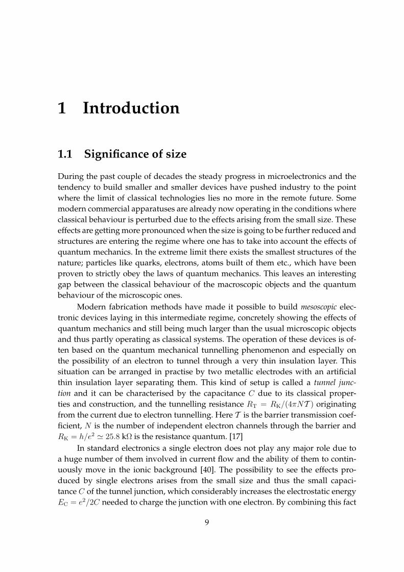
To observe the charging effects of single electrons to its full extent it is not enoughto satisfy the relation Eq. (1.1). In addition, it is necessary to have a metallic islandgalvanically separated from other metallic regions so that the charge on the islandcan change only by electron tunnelling via tunnel junction or junctions. Also thetunnelling resistance of the junction has to be larger than the resistance quantum,RT RK, to have the wave function of an electron to be localised on the island.
Vg
Cg C RT
n
FIGURE 1.1 Single electron box consisting of one tunnel junction in series with a gatecapacitance Cg and a voltage source Vg. The number of excess electrons on the islandis n.
The simplest structure fulfilling these requirements is a so-called single elec-tron box (SEB) consisting of one tunnel junction in series with a gate capacitanceCg and a voltage source Vg as shown in Fig. 1.1. The total charge of the island isnow quantised and characterised by the number of excess electrons n on the island,associated with a charging energy EC = e2/2(C + Cg). The effect of the voltage Vg
is to change the polarisation charge in the gate capacitance and thus the effectivecharge of the junction becomes Q = VgCg − ne. The charging energy of the wholecircuit can be calculated by treating the junction as a regular capacitance after thelast tunnelling, and it obtains a form
ECh =(VgCg − ne)2
2(Cg + C). (1.2)
1.2. BASIC NORMAL-METAL SINGLE ELECTRON DEVICES 11
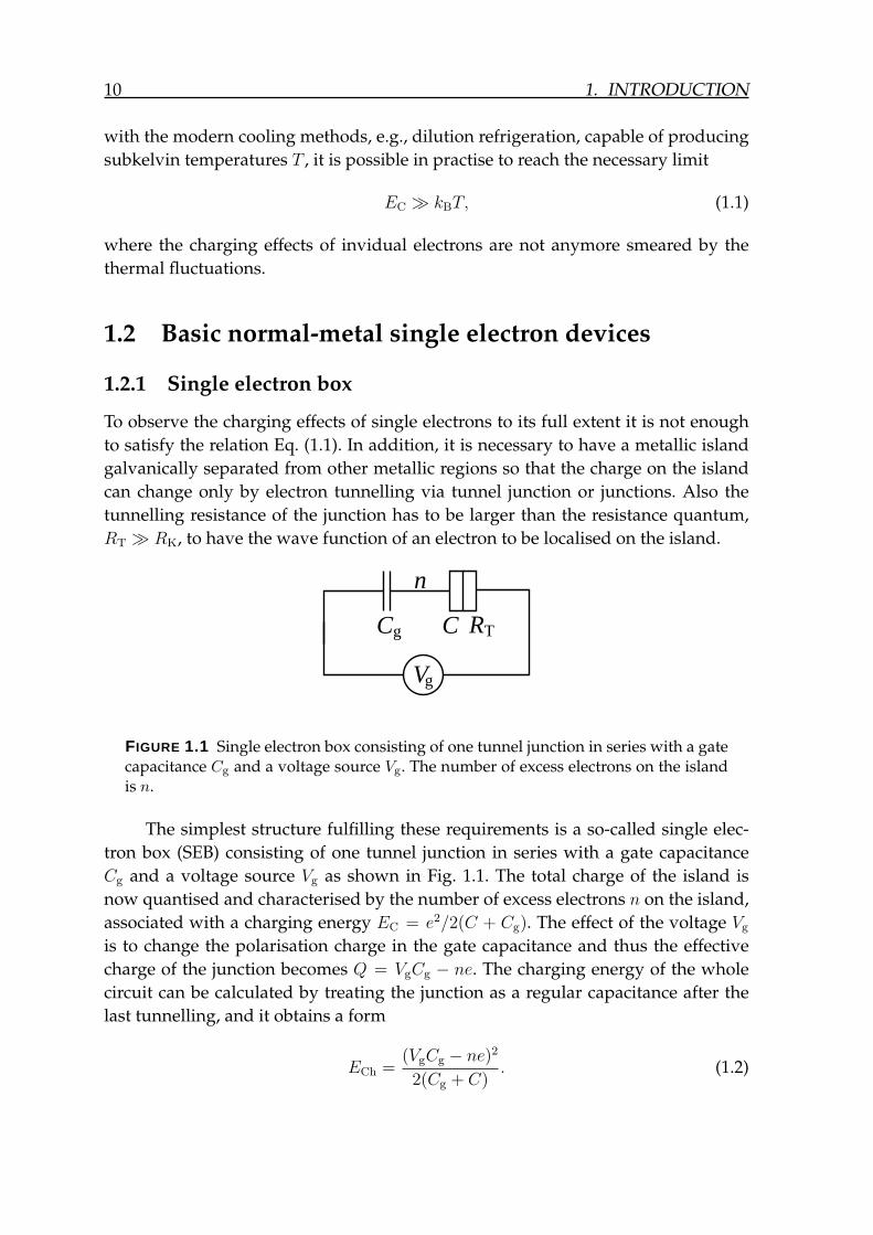
0 1 2 3 40.00
0.25
0.50
0.75
VgCg/e
/EC
EC
h
FIGURE 1.2 Charging energy of the single electron box consisting of a set of parabolaseach corresponding to a certain value of n given by the x coordinate at the minimum.EC = e2/2(C + Cg) is the charging energy of the SEB.
This represents a set of parabolas as a function of Vg, each one corresponding toa certain value of n. These parabolas are separated by Cg/e in x direction as depictedin Fig. 1.2. From the figure one can immediately see that the number of electrons n isstable, yielding the minimum energy if the voltage is between e(n − 1/2) < VgCg <
e(n+1/2). As soon as Vg reaches the value e(n+1/2)/Cg, an electron tunnels into theisland and n is increased by one, i.e., one electron has been ‘added to the box’. Thus,it is possible to control the number of electrons on the island one by one by thevoltage Vg. At zero temperature this control is accurate but at finite temperaturesthe sharp changes in n are smeared by Boltzmann distribution. This quantisationof the island charge and controlling it by the gate voltage was first demonstratedexperimentally in [90].
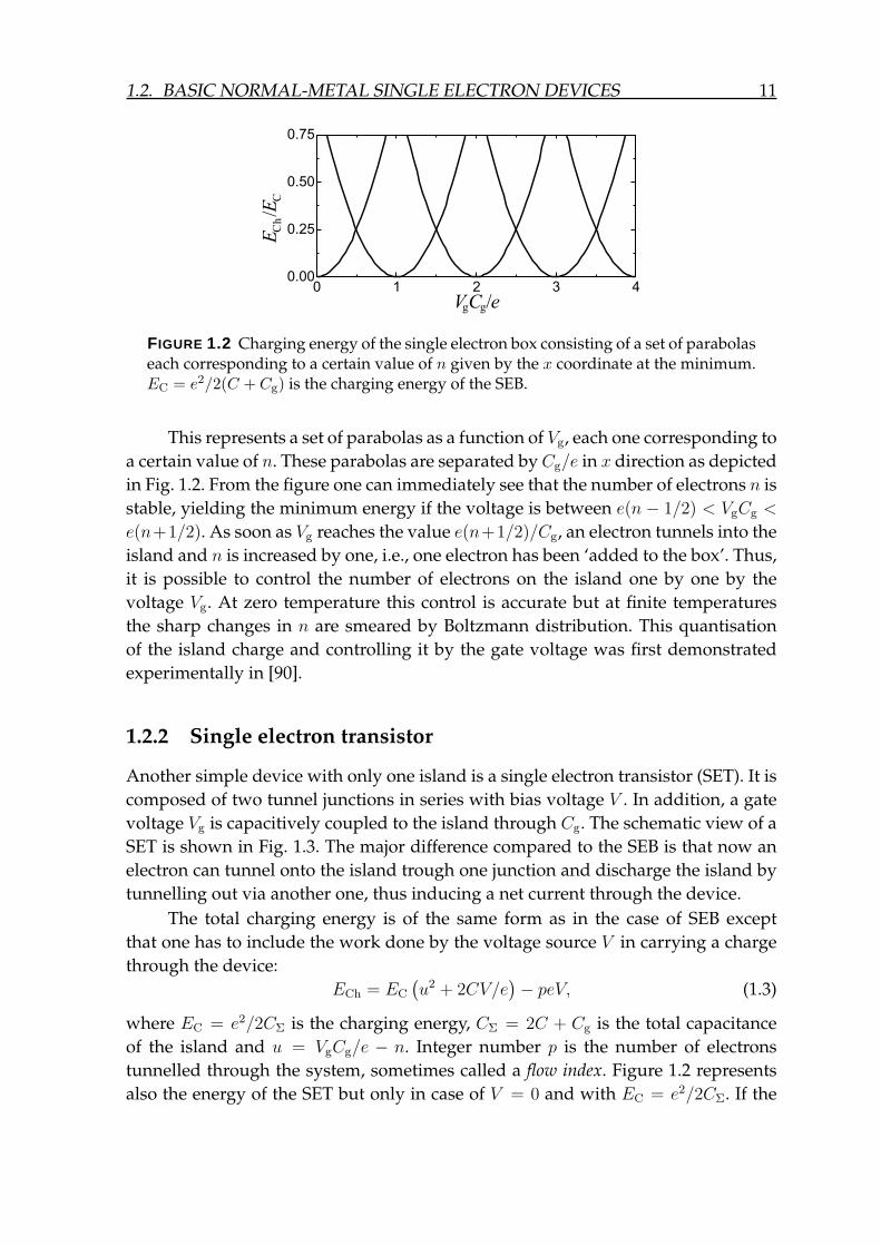
1.2.2 Single electron transistor
Another simple device with only one island is a single electron transistor (SET). It iscomposed of two tunnel junctions in series with bias voltage V . In addition, a gatevoltage Vg is capacitively coupled to the island through Cg. The schematic view of aSET is shown in Fig. 1.3. The major difference compared to the SEB is that now anelectron can tunnel onto the island trough one junction and discharge the island bytunnelling out via another one, thus inducing a net current through the device.
The total charging energy is of the same form as in the case of SEB exceptthat one has to include the work done by the voltage source V in carrying a chargethrough the device:
ECh = EC
(u2 + 2CV/e
)− peV, (1.3)
where EC = e2/2CΣ is the charging energy, CΣ = 2C + Cg is the total capacitanceof the island and u = VgCg/e − n. Integer number p is the number of electronstunnelled through the system, sometimes called a flow index. Figure 1.2 representsalso the energy of the SET but only in case of V = 0 and with EC = e2/2CΣ. If the
12 1. INTRODUCTION
Cg
C CRT RTn
Vg
V/2−V/2
FIGURE 1.3 Schematic view of a single electron transistor. The system is assumedto be symmetric with both junctions having the same capacitance C and tunnellingresistance RT. The gate voltage Vg is connected to the island through capacitance Cg
and the system is biased with voltage V .
gate voltage is zero, Vg = 0, the energy ofEC−eV/2 is needed to charge the island byone electron. At zero temperature this energy has to be provided by the bias voltage,and therefore the current cannot flow, if |V | is smaller than e/CΣ. At voltages abovethat the current is linear, i.e., ohmic with an offset±e/CΣ and a slope determined bythe tunnelling resistance, I = V/RT± e/CΣ. This phenomenon of suppression of thecurrent at small voltages is called Coulomb blockade and it makes it possible to havea well fixed number of electrons n on the island.
As in the case of SEB the gate voltage can be used to change the effective chargeof the island as seen in Eq. 1.3. This makes the threshold voltage of Coulomb block-ade depend on the gate charge. By electrostatic considerations one finds that n isstable inside the regions
e(n− 1
2
)< 1
2CΣV + CgVg < e
(n+ 1
2
). (1.4)
This represents rhombic shaped regions in (V, Vg) plane and inside each region acertain n is stable and no current is flowing. This also makes possible to control thecurrent by the gate voltage Vg at a suitably fixed bias voltage V [77]. That is why thedevice is called single electron transistor and it was first demonstrated experimen-tally already in 1987 [60].
Since at certain voltages near the Coulomb threshold the current is very sen-sitive to the gate voltage, it is possible to use the SET as an ultrasensitive electrom-eter [41, 87, 113] by connecting the system under study capacitively to the island.Due to this property the SET is also suggested to be used as a read-out device of aquantum bit consisting of the superconducting SEB ("squbit") [96, 116].
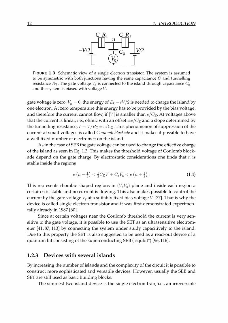
1.2.3 Devices with several islands
By increasing the number of islands and the complexity of the circuit it is possible toconstruct more sophisticated and versatile devices. However, usually the SEB andSET are still used as basic building blocks.
The simplest two island device is the single electron trap, i.e., an irreversible
1.2. BASIC NORMAL-METAL SINGLE ELECTRON DEVICES 13
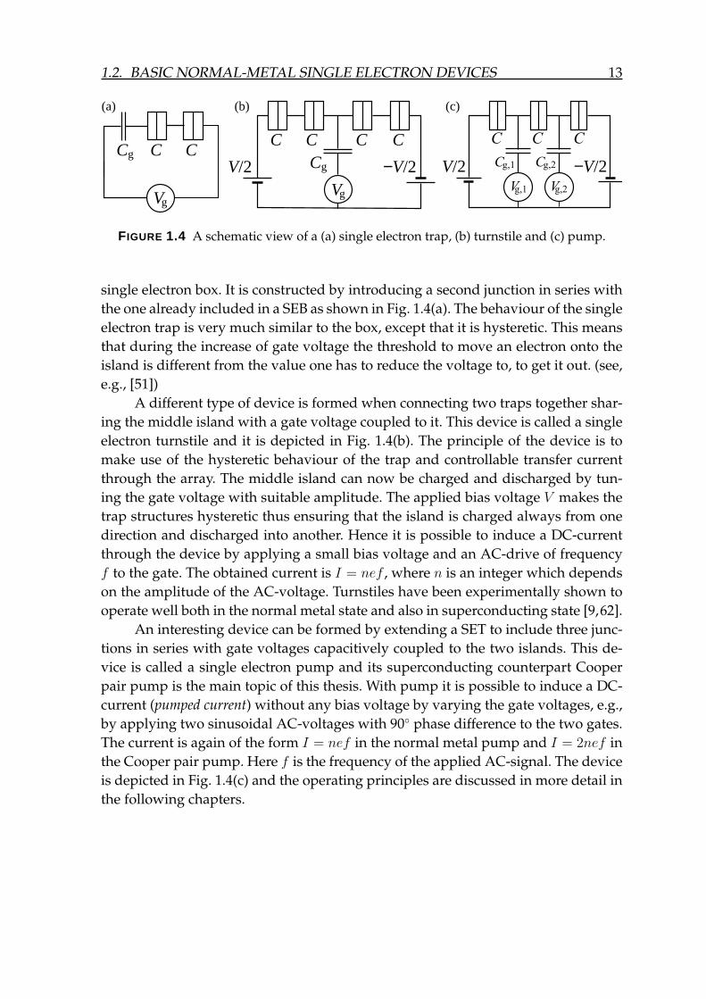
(a) (b) (c)
V/2 −V/2Cg
C C C C
Vg
V/2 −V/2
Vg
Cg C C
FIGURE 1.4 A schematic view of a (a) single electron trap, (b) turnstile and (c) pump.
single electron box. It is constructed by introducing a second junction in series withthe one already included in a SEB as shown in Fig. 1.4(a). The behaviour of the singleelectron trap is very much similar to the box, except that it is hysteretic. This meansthat during the increase of gate voltage the threshold to move an electron onto theisland is different from the value one has to reduce the voltage to, to get it out. (see,e.g., [51])
A different type of device is formed when connecting two traps together shar-ing the middle island with a gate voltage coupled to it. This device is called a singleelectron turnstile and it is depicted in Fig. 1.4(b). The principle of the device is tomake use of the hysteretic behaviour of the trap and controllable transfer currentthrough the array. The middle island can now be charged and discharged by tun-ing the gate voltage with suitable amplitude. The applied bias voltage V makes thetrap structures hysteretic thus ensuring that the island is charged always from onedirection and discharged into another. Hence it is possible to induce a DC-currentthrough the device by applying a small bias voltage and an AC-drive of frequencyf to the gate. The obtained current is I = nef , where n is an integer which dependson the amplitude of the AC-voltage. Turnstiles have been experimentally shown tooperate well both in the normal metal state and also in superconducting state [9,62].
An interesting device can be formed by extending a SET to include three junc-tions in series with gate voltages capacitively coupled to the two islands. This de-vice is called a single electron pump and its superconducting counterpart Cooperpair pump is the main topic of this thesis. With pump it is possible to induce a DC-current (pumped current) without any bias voltage by varying the gate voltages, e.g.,by applying two sinusoidal AC-voltages with 90 phase difference to the two gates.The current is again of the form I = nef in the normal metal pump and I = 2nef inthe Cooper pair pump. Here f is the frequency of the applied AC-signal. The deviceis depicted in Fig. 1.4(c) and the operating principles are discussed in more detail inthe following chapters.

14 1. INTRODUCTION
2 Josephson tunnelling
2.1 Superconductivity
Superconductivity was observed for the first time in 1911 by Kamerlingh Onnes inLeiden [105,106,107], when he noted the resistance of mercury to completely disap-pear below the temperature of liquefied helium. Since that, this same phenomenonof vanishing of resistance in a small temperature range at a so-called critical temper-ature Tc has been observed in many metals and compounds. The critical temperatureis a characteristic of the material and the perfect conductivity at temperatures belowit has been proven by the current flowing in the superconducting ring over a yearwithout any attenuation. The measured decay constant of this supercurrent was notless than 100,000 years [56].
Another important property of a superconductor is the perfect diamagnetism[98], i.e., any magnetic field inside the metal is expelled as the metal is turned intothe superconducting state. This is called Meissner effect and it predicts the supercon-ductivity to be destroyed in magnetic fields higher than the so-called critical field Hc.This has been experimentally verified and temperature dependence of the criticalfield has been empirically found to obey the formula Hc(T ) ≈ Hc(0)
[1− (T/Tc)
2] intype I superconductors. In type II superconductors vortices are formed at magneticfields between the two critical fields Hc,1 and Hc,2. The vortices existing in this mixedstate of superconductor, are normal in their center, thus enabling a flux quantumΦ0 = h/(2e) to penetrate though the superconductor inside each of them. At secondcritical field the maximum density of vortices is reached and the material becomesnormal.
There exists two main theories about the classical superconductivity. The BCStheory by Bardeen, Cooper and Schrieffer [23] is based on the microscopic propertiesof the Fermi-sea of electrons. It shows that even a very weak attractive interactionbetween electrons, e.g., the second order interaction via lattice phonons, causes elec-trons to form pairs, so-called Cooper pairs at low enough temperatures. These pairsare formed by electrons with opposite momentum and spin, and as a consequenceof this pairing an energy gap ∆ is opened around the Fermi surface in the densityof quasiparticle states. The spatial extension of Cooper pairs is of the order of thecoherence length ξ0 = 2~vF/π∆, where vF is the Fermi velocity. The zero resistiv-ity can be qualitatively explained by the Cooper pairs having a total spin of one and
15
16 2. JOSEPHSON TUNNELLING
thus acting like bosons, which condense to Fermi surface at low temperatures. Thesecondensated ‘bosons’ do not interact with each other so they can conduct electricitywithout any attenuation. The most important prediction of the theory is the mini-mum energy 2∆(T ) needed to break the pair, which induces a gap in the density ofquasiparticle states. This gap increases from the zero at Tc to the maximum value of2∆(0) = 3.528kBTc. Theory also yields the correct value for the jump in specific heatat Tc and the Meissner effect [98] can be derived from it. The principles of the BCStheory have also been successfully applied to explain superfluids [99, 130].
The other theory, Ginzburg-Landau (GL) theory [65] is more phenomenologi-cal and introduces a complex pseudowavefunction ψ as an order parameter in Lan-dau’s general theory of second order phase transitions. It is based on the variationalprinciple and on the expansion of the free energy in powers of ψ and∇ψ. GL theoryalso includes coherence length defined as ξ(T ) = ~|2m∗α(T )|−1/2, which charac-terises the distance over which ψ(~r) can vary without undue energy increase. Herem∗ is the mass of the superconducting charge carriers (∼2melectron) and α(T ) is thetemperature dependent constant determined by the GL equation [65].
2.1.1 AC and DC Josephson effects
When two large superconductors with phases ϕ1 and ϕ2 of the (GL) order param-eter ψ(~r) = |ψ(~r)|eiϕ(~r), describing the collective state of the (BCS) Cooper pairs,are weakly connected to each other through the so-called Josephson junction [79], thesupercurrent of the form
Is = Ic sin(ϕ2 − ϕ1) (2.1)
is induced between these superconductors. In principle Josephson junction can beany kind of a weak link, but in this work it consists of a regular tunnel junction,described earlier in Ch. 1, with both electrodes made of a superconductor. The su-percurrent Is arises due to the overlap of the two wavefunctions across the junctionand their interference with each other. The critical current Ic is the maximum currentthat the junction can support.
This same line of reasoning leads also to another important result: if voltage isapplied across the Josephson junction the phase difference δϕ = ϕ1 − ϕ2 will evolveaccording to
dδϕ
dt=
2eV
~. (2.2)
The two effects determined by Eqs. (2.1) and (2.2) are called the DC and AC Josephsoneffects and they were experimentally verified shortly after Josephson’s prediction in[79]. The modern Josephson voltage standard used in many institutes of metrology,is based on these effects.
From (2.1) and (2.2) one can also derive the electrical work done by the currentsource and thus the energy stored in the junction while the δϕ is changing. This can
2.2. EXPERIMENTAL TECHNIQUES 17
be obtained by integrating∫IsV dt =
∫Is~/(2e)d(δϕ), which yields
E = −EJ cos δϕ, (2.3)
where EJ ≡ ~Ic/2e is the Josephson coupling energy.
2.1.2 Ambegaokar-Baratoff formula
From the GL theory [65] one can derive the critical current Ic for the general weaklink, ‘bridge’ in this case, of length L ξ and with the cross-sectional area of A:
Ic = (2e~ψ2∞/m
∗)(A/L), (2.4)
where ψ∞ is the absolute value of the order parameter in both superconductors.By applying a similar reasoning to the case of tunnel junction, Ambegaokar andBaratoff worked out the expression for the critical current and thus for EJ in aJosephson tunnel junction [8]. The general expression with the two electrodes hav-ing energy gaps ∆1 and ∆2 can be obtained in the limit kBT ∆1,∆2 [44]
EJ =2RQ
πRT
∆1∆2
∆1 + ∆2
K(|∆1 −∆2|∆1 + ∆2
). (2.5)
Here RQ = h/(2e)2 ≈ 6.5 kΩ is the resistance quantum for the Cooper pairs andK(x) is the complete elliptic integral of the first kind. In the case of identical super-conductors, ∆1 = ∆2 ≡ ∆, one obtains a general expression at any T
EJ =∆
2
RQ
RT
tanh
(∆
2kBT
). (2.6)
2.2 Experimental techniques
Since the following sections treating the properties of the superconducting singlecharge, i.e., single Cooper pair devices involves also experimental data, it is usefulto discuss the particular experimental principles at this point.
2.2.1 Sample fabrication
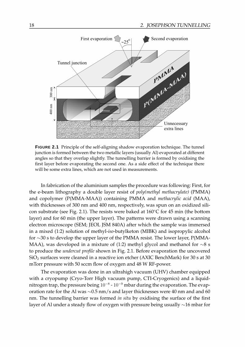
All the samples used in the experiments of this thesis were fabricated using electronbeam lithography and self-aligning shadow evaporation techniques [43], which isthe most commonly used combination of methods in fabrication of tunnel junctions.The basic shadow evaporation technique, in which two different evaporation anglesare used with a stencil mask to form a tunnel junction between the tiny overlappingareas of the evaporated wires, is illustrated in Fig. 2.1.
18 2. JOSEPHSON TUNNELLING
°
Tunnel junction
40
0 n
m3
00
nm
Unnecessaryextra lines
~25First evaporation Second evaporation
FIGURE 2.1 Principle of the self-aligning shadow evaporation technique. The tunneljunction is formed between the two metallic layers (usually Al) evaporated at differentangles so that they overlap slightly. The tunnelling barrier is formed by oxidising thefirst layer before evaporating the second one. As a side effect of the technique therewill be some extra lines, which are not used in measurements.
In fabrication of the aluminium samples the procedure was following: First, forthe e-beam lithography a double layer resist of poly(methyl methacrylate) (PMMA)and copolymer (P(MMA-MAA)) containing PMMA and methacrylic acid (MAA),with thicknesses of 300 nm and 400 nm, respectively, was spun on an oxidized sili-con substrate (see Fig. 2.1). The resists were baked at 160C for 45 min (the bottomlayer) and for 60 min (the upper layer). The patterns were drawn using a scanningelectron microscope (SEM; JEOL JSM 840A) after which the sample was immersedin a mixed (1:2) solution of methyl-iso-butylketon (MIBK) and isopropylic alcoholfor ∼30 s to develop the upper layer of the PMMA resist. The lower layer, P(MMA-MAA), was developed in a mixture of (1:2) methyl glycol and methanol for ∼8 sto produce the undercut profile shown in Fig. 2.1. Before evaporation the uncoveredSiO2 surfaces were cleaned in a reactive ion etcher (AXIC BenchMark) for 30 s at 30mTorr pressure with 50 sccm flow of oxygen and 48 W RF-power.
The evaporation was done in an ultrahigh vacuum (UHV) chamber equippedwith a cryopump (Cryo-Torr High vacuum pump, CTI-Cryogenics) and a liquid-nitrogen trap, the pressure being 10−8 - 10−9 mbar during the evaporation. The evap-oration rate for the Al was ∼0.5 nm/s and layer thicknesses were 40 nm and and 60nm. The tunnelling barrier was formed in situ by oxidising the surface of the firstlayer of Al under a steady flow of oxygen with pressure being usually ∼16 mbar for
2.2. EXPERIMENTAL TECHNIQUES 19
three minutes. This produces a 1 - 2 nm thick layer of insulating AlOx, which actsas a tunnelling barrier. The oxidation parameters were slightly varied from sampleto sample to obtain desired resistances. The process was completed by the lift-off, inwhich the sample was immersed in a warmed acetone to remove all the resists andthe extra metal at the top of it, and final cleaning by reactive ion etching, with sameparameters as before, to remove all the remnants of the resist.
In fabrication of the Cooper pair pump measured in Ref. [6] and briefly re-viewed in chapter 6 the extra ex situ process was included to first pattern the largerstructures; the contact pads, grounded shielding planes and gate lines for RF-signals.These structures were fabricated using the same method as described above exceptthat only one angle was needed in evaporation and the material was chosen to begold to prevent any possible problems with large superconducting planes and toensure good electrical contact to the small Al structures. Also a thin layer of tita-nium was evaporated under the gold to improve adhesion. After that the sampleitself was fabricated on top of this structure using the regular shadow evaporationprocessing with an extra aligning process step.
The self-aligning shadow evaporation method has been successfully appliedfor soft metals like Cu, Pb and Al, the last one being the most common materialin single electron devices since it can be operated both in the normal and in thesuperconducting state, and especially because it easily forms a relatively stable tun-nel barrier. However, recent developments in the field of superconducting deviceshave raised a new demand for a more suitable material with larger energy gap, ∆.One candidate for this is niobium (Nb) since its critical temperature is as high as9.3 K yielding ∼1.5 meV for the gap, which is much higher than the 0.2 meV gapof aluminium. Yet, it is known to be difficult to apply self alignment technique forrefractory metals like Nb due to a poor film quality usually obtained using it.
This deterioration of the Nb film is manifested as critical temperature Tc andthus the energy gap ∆ being far below the bulk value [45, 72, 83]. One problem isthe contamination of the Nb film by outgassing from the resists during the evapo-ration [45, 83]. To overcome this the authors of Refs. [45] and [44] used trilayer re-sist with bottom layer made of thermostable phenylen-ether-sulfone (PES) polymer,which has a glass temperature and decomposition temperature much higher thanthose of PMMA resist. By fabricating Nb wires with this process they reached Tc of8.2 K. However, the process itself is more complicated than the conventional PMMAprocess. Even more complicated method was developed by authors of Ref. [109]where they used spin-on glass planarisation technique and several ex situ processsteps to form wiring between vertical Nb/Al/AlOx/Nb-junctions fabricated in situ.Advantage of this process is the reliability of the insulating layer and the high qual-ity of the superconducting Nb electrodes. Yet using this process it is difficult to re-duce the size of the junction from (300× 300) µm2 and thus to increase the chargingenergy EC, which is essential for single charge devices.
20 2. JOSEPHSON TUNNELLING
Almost all the earlier reports on the fabrication of superconducting single elec-tron devices using niobium have come to a conclusion that it is not possible tomake high quality Nb-based devices using conventional shadow evaporation tech-nique with PMMA as a resist. Nevertheless, the Al/Nb/Al SETs used in the experi-ments in Ref. [7] and in chapter 3, were fabricated with regular shadow evaporationtechnique but along a slightly more sophisticated process compared to the sam-ples made of aluminium. The modifications in fabrication process included slightlythicker bottom layer of the resist and thicker SiO2 layer at the substrate, to providelarger undercut, which is essential for the fabrication ensuring the removal of rem-nants of the resist and therefore, reducing the outgassing during the evaporation.The outgassing was even more reduced by using a long distance (&40 cm) betweenthe Nb source and the sample during the evaporation thus reducing temperature ofthe evaporated Nb hitting the sample. To be on the safe side couple of extra stepswere also performed, but the effectiveness of them is not very clear. After the etch-ing and just before the evaporation, the mask was baked below 90 for 30 min to getrid of the possible moisture and to glaze the mask to endure the excessive heatingby the niobium at the evaporation. The aluminum leads were evaporated first toenable the forming of the tunnelling barrier by oxidation and to provide an extraprotective layer at the top of the resist, while evaporating the niobium. To ensurethe stability and hardness of the evaporated Al layer it was let to cool down for atleast 5 minutes before evaporating Nb.
2.2.2 Measurement setups
All the measurements included in this thesis were done at temperatures below 10K using two different dilution refrigerators with different measurement setups. Themeasurements included in this chapter and in chapter 3 [7] were carried out in asmall dilution refrigerator (Nanoway, PDR50) with the base temperature slightlybelow 100 mK. The temperature was usually measured using a resistance bridge(Picowatt AVS-47) and a carbon resistor, calibrated against the primary Coulombblockade thermometer (Nanoway CBT). In measurements of chapter 3, we useda commercial calibrated Cernox resistor with good thermal anchoring in the veryvicinity of the sample. Current and voltage measurements were done using thebattery powered DL-Instrument’s 1211 current preamplifier and the 1201 low-noisepreamplifier, respectively.
The fridge was placed inside an electrically shielded room (Euroshield) whichprovided low external noise level for the measurements. The preamplified signalswere conducted out of the shielded room through the highly efficient low pass filters(Euroshield) mounted in the wall and fed to the data acquisition card in a computer(NI PCI-6035E DAQ card). All the measuring wires in the cryostat contained com-mercial π-filters at room temperature and at 4.2 K. To reduce a heat leak, resistive
2.2. EXPERIMENTAL TECHNIQUES 21
manganin wires were used between the filters. These wires were placed inside aCuNi tube for electric shielding. In addition, so-called strip filters were mountedinto the lines at the sample stage and in measurements of chapter 3 also at the 1kelvin plate. These filters were commercial stress gauges (KYOWA KFG-2-350-D1-23 and KFG-2-120-D1-23) squeezed between two ground planes forming continuousRC strip line filters [129]. The mounting of the sample was done using ultrasonicbonding with aluminium wires.
The measurements of the Cooper pair pump were carried out in an S.H.E.Corporation DRI-420 dilution refrigerator whose minimum temperature is∼10 mK.Temperature was measured using directly the primary CBT thermometer or the car-bon resistor calibrated by it. No shielded room was used, but the lower parts of thecryostat were surrounded by lead over the vacuum jacket in the helium bath forextra magnetic shielding. Due to the more sensitive measurements and the lack ofshielded room an extra attention was paid to the filtering involved in the wiring.
The fridge has 14 highly filtered lines for DC-signals (Fig. 2.2 (a)). These linesinclude low pass filtering at three different temperatures. At room temperature weused again commercial low pass π-filters (Tusonix 4101, -55 dB at 100 MHz) whichwere connected directly at the top of the cryostat. From room temperature down to600 mK all DC-signals are fed through coaxial cables with Nb as an inner conductorand stainless steel as the outer one. Between 600 mK and 60 mK plate we have 1.5 mlong pieces of Thermocoax cable which also form the next filtering stage (-200 dB at20 GHz) [134]. At both ends of Thermocoax cables there are 1 kΩ resistors in seriesto improve filtering at low frequencies (100 kHz . f < 1 GHz). The last filteringstage is at the sample stage at the base temperature. As before, these filters werecontinuous RC strip line filters made of commercial stress gauges (KYOWA KFG-2-350-D1-23). Short wires at the sample stage were made of Cu and were solderedto a printed circuit board (PCB). This again was ultrasonically bonded to the DCelectrode of the sample with aluminium wires.
DRI-420 refrigerator has also four lines for RF-signals (Fig. 2.2 (a)). At roomtemperature we used 400 MHz low pass filters (Mini-circuits SBLP-400) and -6 dBfixed attenuators (Inmet). These were directly connected to the top of the cryostatand all other room temperature connections were made by using flexible SUHNERSucoflex 104P cables with SMA connectors. From room temperature down to 4.2K RF-signals are fed through Cu coaxial cables. At low temperatures we use BeCucoaxial cables, except that between 600 mK and the sample stage we use semirigidstainless steel coaxial cables for better thermal isolation. As a whole the RF lineshave -33 dB attenuation at low temperatures: -20 dB at 4.2 K, -10 dB at 600 mK and-3 dB at the sample stage temperature (Inmet fixed attenuators). At the sample stageMCX connectors are used and all other connectors are of SMA type. The sample isdirectly ultrasonically bonded by Al bonding wire to a co-planar transmission linemounted on the sample stage. When all these lines are connected to the coldest parts
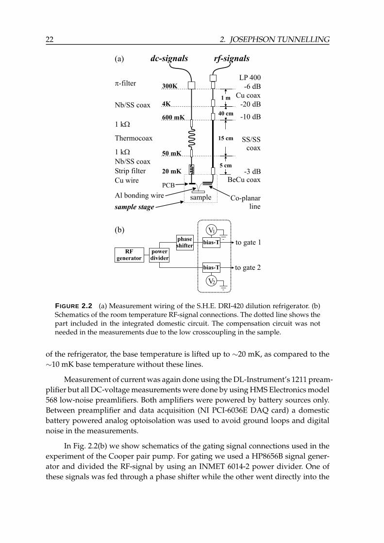
22 2. JOSEPHSON TUNNELLING
(a)
(b)
RFgenerator
to gate 2
powerdivider
phaseshifter
V1
V2
to gate 1
bias-T
bias-T
20 mK
50 mK
600 mK
4K
300K
-10 dB
-20 dB
-6 dB
LP 400
-3 dBBeCu coax
SS/SScoax
Co-planarline
PCB
Thermocoax
Strip filter
Cu wire
1 kW
1 kW
Nb/SS coax
p-filter
Nb/SS coax
sample stage
Al bonding wire sample
rf-signalsdc-signals
1 m Cu coax
40 cm
15 cm
5 cm
FIGURE 2.2 (a) Measurement wiring of the S.H.E. DRI-420 dilution refrigerator. (b)Schematics of the room temperature RF-signal connections. The dotted line shows thepart included in the integrated domestic circuit. The compensation circuit was notneeded in the measurements due to the low crosscoupling in the sample.
of the refrigerator, the base temperature is lifted up to ∼20 mK, as compared to the∼10 mK base temperature without these lines.
Measurement of current was again done using the DL-Instrument’s 1211 pream-plifier but all DC-voltage measurements were done by using HMS Electronics model568 low-noise preamlifiers. Both amplifiers were powered by battery sources only.Between preamplifier and data acquisition (NI PCI-6036E DAQ card) a domesticbattery powered analog optoisolation was used to avoid ground loops and digitalnoise in the measurements.
In Fig. 2.2(b) we show schematics of the gating signal connections used in theexperiment of the Cooper pair pump. For gating we used a HP8656B signal gener-ator and divided the RF-signal by using an INMET 6014-2 power divider. One ofthese signals was fed through a phase shifter while the other went directly into the
2.3. SUPERCONDUCTING SINGLE ISLAND DEVICES 23
custom made circuit 1 schematically consisting of two bias-Ts and a possibility toadd negative crosscoupling between the two signals to compensate for the undesir-able capacitive coupling between the gates in the CPP. The circuit also contained ahigh quality RF-circuit-board and optoisolated linking to the computer, which couldbe used to program all the gains used in bias-Ts, DC-offsets, compensation and asa main amplification. The control program2 also included a possibility to automatethe measurements.
2.3 Superconducting single island devices
eV
SET =⇒ SSET
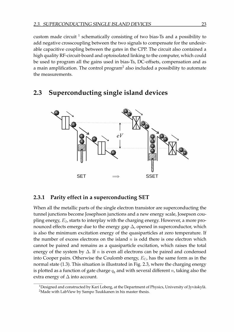
2.3.1 Parity effect in a superconducting SET
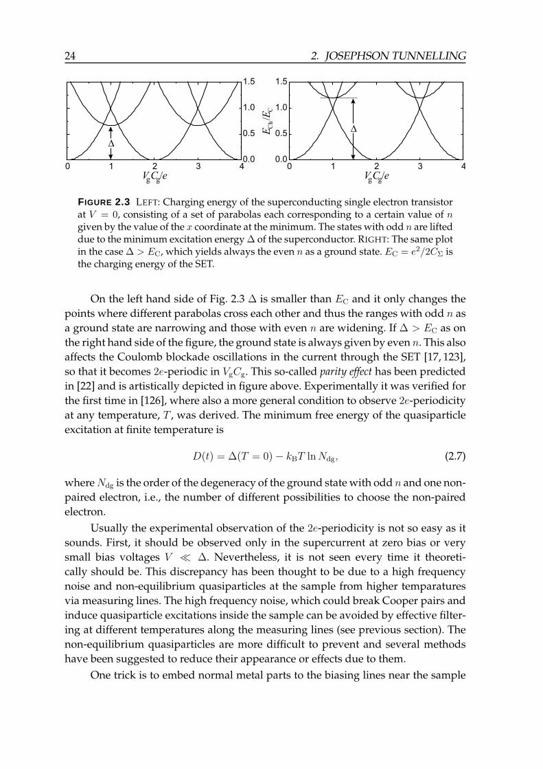
When all the metallic parts of the single electron transistor are superconducting thetunnel junctions become Josephson junctions and a new energy scale, Josepson cou-pling energy, EJ, starts to interplay with the charging energy. However, a more pro-nounced effects emerge due to the energy gap ∆, opened in superconductor, whichis also the minimum excitation energy of the quasiparticles at zero temperature. Ifthe number of excess electrons on the island n is odd there is one electron whichcannot be paired and remains as a quasiparticle excitation, which raises the totalenergy of the system by ∆. If n is even all electrons can be paired and condensedinto Cooper pairs. Otherwise the Coulomb energy, EC, has the same form as in thenormal state (1.3). This situation is illustrated in Fig. 2.3, where the charging energyis plotted as a function of gate charge qg and with several different n, taking also theextra energy of ∆ into account.
1Designed and constructed by Kari Loberg, at the Department of Physics, University of Jyväskylä.2Made with LabView by Sampo Tuukkanen in his master thesis.
24 2. JOSEPHSON TUNNELLING
0 1 2 3 40.0
0.5
1.0
1.5
VgCg/e
D
0 1 2 3 40.0
0.5
1.0
1.5
VgCg/e
D
/EC
EC
h
FIGURE 2.3 LEFT: Charging energy of the superconducting single electron transistorat V = 0, consisting of a set of parabolas each corresponding to a certain value of ngiven by the value of the x coordinate at the minimum. The states with odd n are lifteddue to the minimum excitation energy ∆ of the superconductor. RIGHT: The same plotin the case ∆ > EC, which yields always the even n as a ground state. EC = e2/2CΣ isthe charging energy of the SET.
On the left hand side of Fig. 2.3 ∆ is smaller than EC and it only changes thepoints where different parabolas cross each other and thus the ranges with odd n asa ground state are narrowing and those with even n are widening. If ∆ > EC as onthe right hand side of the figure, the ground state is always given by even n. This alsoaffects the Coulomb blockade oscillations in the current through the SET [17, 123],so that it becomes 2e-periodic in VgCg. This so-called parity effect has been predictedin [22] and is artistically depicted in figure above. Experimentally it was verified forthe first time in [126], where also a more general condition to observe 2e-periodicityat any temperature, T , was derived. The minimum free energy of the quasiparticleexcitation at finite temperature is
D(t) = ∆(T = 0)− kBT lnNdg, (2.7)
whereNdg is the order of the degeneracy of the ground state with odd n and one non-paired electron, i.e., the number of different possibilities to choose the non-pairedelectron.
Usually the experimental observation of the 2e-periodicity is not so easy as itsounds. First, it should be observed only in the supercurrent at zero bias or verysmall bias voltages V ∆. Nevertheless, it is not seen every time it theoreti-cally should be. This discrepancy has been thought to be due to a high frequencynoise and non-equilibrium quasiparticles at the sample from higher temparaturesvia measuring lines. The high frequency noise, which could break Cooper pairs andinduce quasiparticle excitations inside the sample can be avoided by effective filter-ing at different temperatures along the measuring lines (see previous section). Thenon-equilibrium quasiparticles are more difficult to prevent and several methodshave been suggested to reduce their appearance or effects due to them.
One trick is to embed normal metal parts to the biasing lines near the sample
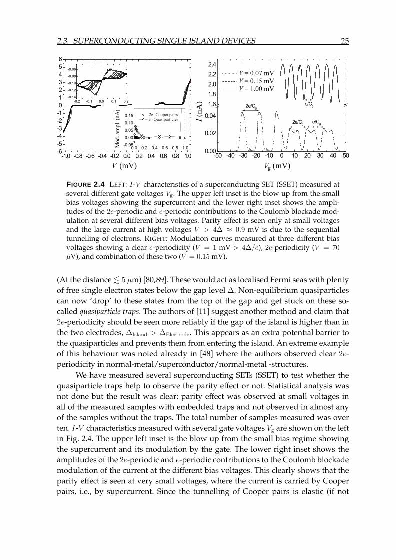
2.3. SUPERCONDUCTING SINGLE ISLAND DEVICES 25
I(n
A)
Vg (mV)
.
.
.
.
.
.
.
.
V (mV)
-1.0 -0.8 -0.6 -0.4 -0.2 0.0 0.2 0.4 0.6 0.8 1.0-6
-5
-4
-3
-2
-1
0
1
2
3
4
5
6
-0.2 -0.1 0.0 0.1 0.2
-0.14
-0.12
-0.10
-0.08
-0.06
0.0 0.2 0.4 0.6 0.8 1.0-0.05
0.00
0.05
0.10
0.15 2e -Cooper pairse -Quasiparticles
Mod
.am
pl.
(nA
)
V = 1.00 mV
V = 0.15 mV
V = 0.07 mV
FIGURE 2.4 LEFT: I-V characteristics of a superconducting SET (SSET) measured atseveral different gate voltages Vg. The upper left inset is the blow up from the smallbias voltages showing the supercurrent and the lower right inset shows the ampli-tudes of the 2e-periodic and e-periodic contributions to the Coulomb blockade mod-ulation at several different bias voltages. Parity effect is seen only at small voltagesand the large current at high voltages V > 4∆ ≈ 0.9 mV is due to the sequentialtunnelling of electrons. RIGHT: Modulation curves measured at three different biasvoltages showing a clear e-periodicity (V = 1 mV > 4∆/e), 2e-periodicity (V = 70µV), and combination of these two (V = 0.15 mV).
(At the distance . 5 µm) [80,89]. These would act as localised Fermi seas with plentyof free single electron states below the gap level ∆. Non-equilibrium quasiparticlescan now ‘drop’ to these states from the top of the gap and get stuck on these so-called quasiparticle traps. The authors of [11] suggest another method and claim that2e-periodicity should be seen more reliably if the gap of the island is higher than inthe two electrodes, ∆Island > ∆Electrode. This appears as an extra potential barrier tothe quasiparticles and prevents them from entering the island. An extreme exampleof this behaviour was noted already in [48] where the authors observed clear 2e-periodicity in normal-metal/superconductor/normal-metal -structures.
We have measured several superconducting SETs (SSET) to test whether thequasiparticle traps help to observe the parity effect or not. Statistical analysis wasnot done but the result was clear: parity effect was observed at small voltages inall of the measured samples with embedded traps and not observed in almost anyof the samples without the traps. The total number of samples measured was overten. I-V characteristics measured with several gate voltages Vg are shown on the leftin Fig. 2.4. The upper left inset is the blow up from the small bias regime showingthe supercurrent and its modulation by the gate. The lower right inset shows theamplitudes of the 2e-periodic and e-periodic contributions to the Coulomb blockademodulation of the current at the different bias voltages. This clearly shows that theparity effect is seen at very small voltages, where the current is carried by Cooperpairs, i.e., by supercurrent. Since the tunnelling of Cooper pairs is elastic (if not
26 2. JOSEPHSON TUNNELLING
considering the effect of the electromagnetic environment, which is usually small,see chapter 4.2.1), it is forbidden at the bias voltages significantly different from zero.This is seen as a flat region with almost vanishing current in the I-V curves. Thesymmetric peaks at V ' ±2∆/e are due to so-called Josephson quasiparticle cycle(JQP), where a Cooper pair tunnels through one junction and two quasiparticlesthrough the other. At voltages higher than 4∆/e sequential tunnelling of electronsbecomes possible. This is seen as a steep increase in the current at V = ±4∆/e
and the e-periodic modulation at voltages higher than that proves the current to becarried by electrons. On the right side of the figure we show the modulation curvesmeasured at three different bias voltages exhibiting a clear e-periodicity (V = 1 mV> 4∆/e), 2e-periodicity (V = 70 µV), and a combination of these (V = 0.15 mV).
The simplest Hamiltonian describing the SSET with Josephson coupling reads
H = Hch +HJ. (2.8)
The charging energy part of the Hamiltonian is of the form 〈m|HCh|m〉 = ECh(n =
2m), where ECh(n) is given by Eq. (1.3), and the Josephson part is obtained fromEq. (2.3), HJ = −
∑i=1,2EJ,i cos δϕi. The charge states |m〉, are the eigenstates of the
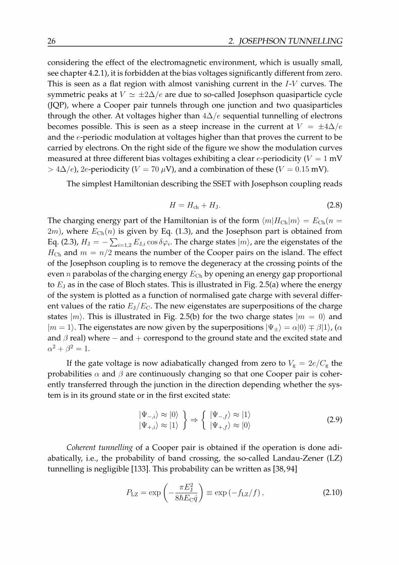
HCh and m = n/2 means the number of the Cooper pairs on the island. The effectof the Josephson coupling is to remove the degeneracy at the crossing points of theeven n parabolas of the charging energyECh by opening an energy gap proportionalto EJ as in the case of Bloch states. This is illustrated in Fig. 2.5(a) where the energyof the system is plotted as a function of normalised gate charge with several differ-ent values of the ratio EJ/EC. The new eigenstates are superpositions of the chargestates |m〉. This is illustrated in Fig. 2.5(b) for the two charge states |m = 0〉 and|m = 1〉. The eigenstates are now given by the superpositions |Ψ±〉 = α|0〉 ∓ β|1〉, (αand β real) where − and + correspond to the ground state and the excited state andα2 + β2 = 1.
If the gate voltage is now adiabatically changed from zero to Vg = 2e/Cg theprobabilities α and β are continuously changing so that one Cooper pair is coher-ently transferred through the junction in the direction depending whether the sys-tem is in its ground state or in the first excited state:
|Ψ−,i〉 ≈ |0〉|Ψ+,i〉 ≈ |1〉
⇒|Ψ−,f〉 ≈ |1〉|Ψ+,f〉 ≈ |0〉
(2.9)
Coherent tunnelling of a Cooper pair is obtained if the operation is done adi-abatically, i.e., the probability of band crossing, the so-called Landau-Zener (LZ)tunnelling is negligible [133]. This probability can be written as [38, 94]
PLZ = exp
(− πE2
J
8~ECq
)≡ exp (−fLZ/f) , (2.10)
2.3. SUPERCONDUCTING SINGLE ISLAND DEVICES 27
0.0 0.2 0.4 0.6 0.8 1.0
0.0
0.2
0.4
0.6
0.8
1.0 EJ/E
C
00.10.21.0
a2
VgCg /2e
/
0.0 0.2 0.4 0.6 0.8 1.0
0.0
0.2
0.4
0.6
0.8
1.0
EE
C
VgCg /2e
EJ/E
C
00.10.2
(a) (b)
FIGURE 2.5 (a) The eigenenergy of the superconducting SET as a function of nor-malised gate charge with several different values of the ratio EJ/EC in the groundstate and in the first excited state. Two charge states, |0〉 and |1〉, are included inthe calculation. (b) The eigenstates of the system are given by the superpositions|Ψ±〉 = α|0〉 ± β|1〉, where α2 + β2 = 1. α2 is plotted as a function of the normalisedgate charge.
where q = VgCg/2e is the normalised gate charge, fLZ is the Landau-Zener frequencydetermined from the equation above and f ∝ q is the operating frequency.
2.3.2 Cooper pair box
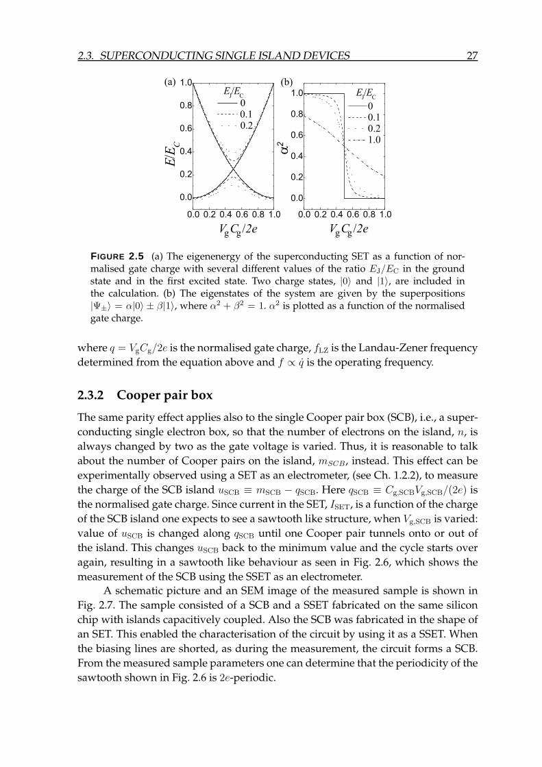
The same parity effect applies also to the single Cooper pair box (SCB), i.e., a super-conducting single electron box, so that the number of electrons on the island, n, isalways changed by two as the gate voltage is varied. Thus, it is reasonable to talkabout the number of Cooper pairs on the island, mSCB, instead. This effect can beexperimentally observed using a SET as an electrometer, (see Ch. 1.2.2), to measurethe charge of the SCB island uSCB ≡ mSCB − qSCB. Here qSCB ≡ Cg,SCBVg,SCB/(2e) isthe normalised gate charge. Since current in the SET, ISET, is a function of the chargeof the SCB island one expects to see a sawtooth like structure, when Vg,SCB is varied:value of uSCB is changed along qSCB until one Cooper pair tunnels onto or out ofthe island. This changes uSCB back to the minimum value and the cycle starts overagain, resulting in a sawtooth like behaviour as seen in Fig. 2.6, which shows themeasurement of the SCB using the SSET as an electrometer.
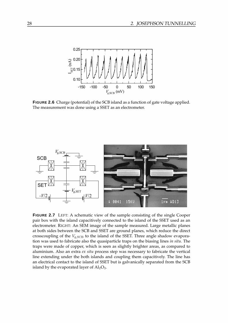
A schematic picture and an SEM image of the measured sample is shown inFig. 2.7. The sample consisted of a SCB and a SSET fabricated on the same siliconchip with islands capacitively coupled. Also the SCB was fabricated in the shape ofan SET. This enabled the characterisation of the circuit by using it as a SSET. Whenthe biasing lines are shorted, as during the measurement, the circuit forms a SCB.From the measured sample parameters one can determine that the periodicity of thesawtooth shown in Fig. 2.6 is 2e-periodic.
28 2. JOSEPHSON TUNNELLING
-1 15 50 0-100 -50 0 50 100
Vg,SCB
SE
T
(mV)
0.10
0.15
0.20
0.25
I(n
A)
FIGURE 2.6 Charge (potential) of the SCB island as a function of gate voltage applied.The measurement was done using a SSET as an electrometer.
SET
SCB
Vg,SET
V/2-V/2
Vg,SCB
FIGURE 2.7 LEFT: A schematic view of the sample consisting of the single Cooperpair box with the island capacitively connected to the island of the SSET used as anelectrometer. RIGHT: An SEM image of the sample measured. Large metallic planesat both sides between the SCB and SSET are ground planes, which reduce the directcrosscoupling of the Vg,SCB to the island of the SSET. Three angle shadow evapora-tion was used to fabricate also the quasiparticle traps on the biasing lines in situ. Thetraps were made of copper, which is seen as slightly brighter areas, as compared toaluminium. Also an extra ex situ process step was necessary to fabricate the verticalline extending under the both islands and coupling them capacitively. The line hasan electrical contact to the island of SSET but is galvanically separated from the SCBisland by the evaporated layer of Al2O3.
3 Superconducting Al/Nb/Al SET
3.1 Benefits of using niobium
In most of the cases the undisturbed manipulation of the Cooper pairs is mandatoryfor the device to operate properly. Therefore, it is important to have a high suppres-sion of quasiparticles. This can be obtained by the parity effect, as discussed in theprevious chapter. However, the parity effect furthermore sets the upper limit for thecharging energy (2.7), which usually also needs to be high. This can be a problemin the case of aluminium and certainly limits the range of useful sample parame-ters. The larger superconducting gap of niobium would push this limit higher andalso provide a better suppression of the quasiparticle tunnelling, since the condition(2.7) is well fulfilled and tolerates better any additional sources of energy, e.g., highfrequency noise.
The larger gap also produces a larger Josephson coupling energy EJ in ultra-small junctions (2.5), which makes it possible to have both the high charging energyand the Josephson energy, and still have the high enough normal state resistance ofthe junctions RT.
3.2 Measurements
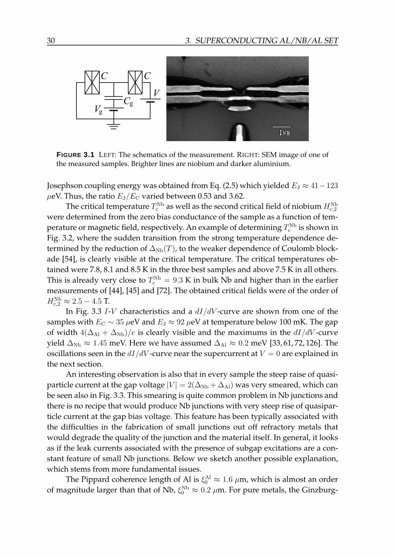
The measured samples were superconducting SETs (SSET) with Nb island and Alelectrodes consisting of two Nb/AlOx/Al junctions. Also the single Nb/AlOx/Aland Al/AlOx/Al junctions as well as all-aluminium SETs were measured as a com-parison. The samples were fabricated along the recipes explained in Ch. 2.2.1 andall the measurements were carried out in a small dilution refrigerator (Nanoway,PDR50) with the base temperature below 100 mK. The measurement setup is ex-plained in detail in Ch. 2.2.2. The schematics of the measurement and the SEM imageof one of the measured SETs is shown in Fig. 3.1.
3.2.1 Characterisation of the samples
The charging energies,EC = e2/(2CΣ), whereCΣ = 2C+Cg, of the SETs were derivedfrom the normal state conductance curve measured at 4.2 K with magnetic field ofB ∼ 5 T [54]. Obtained charging energies varied between EC ≈ 34 − 78 µeV. The
29
30 3. SUPERCONDUCTING AL/NB/AL SET
C
Cg
C
Vg
V
FIGURE 3.1 LEFT: The schematics of the measurement. RIGHT: SEM image of one ofthe measured samples. Brighter lines are niobium and darker aluminium.
Josephson coupling energy was obtained from Eq. (2.5) which yielded EJ ≈ 41−123
µeV. Thus, the ratio EJ/EC varied between 0.53 and 3.62.The critical temperature TNb
c as well as the second critical field of niobium HNbc,2
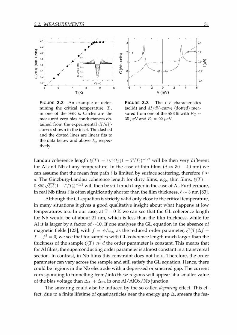
were determined from the zero bias conductance of the sample as a function of tem-perature or magnetic field, respectively. An example of determining TNb
c is shown inFig. 3.2, where the sudden transition from the strong temperature dependence de-termined by the reduction of ∆Nb(T ), to the weaker dependence of Coulomb block-ade [54], is clearly visible at the critical temperature. The critical temperatures ob-tained were 7.8, 8.1 and 8.5 K in the three best samples and above 7.5 K in all others.This is already very close to TNb
c = 9.3 K in bulk Nb and higher than in the earliermeasurements of [44], [45] and [72]. The obtained critical fields were of the order ofHNb
c,2 ≈ 2.5− 4.5 T.In Fig. 3.3 I-V characteristics and a dI/dV -curve are shown from one of the
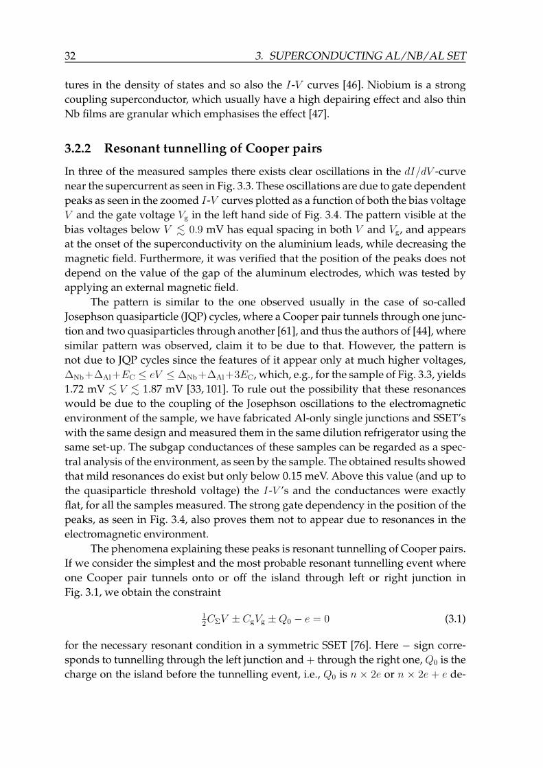
samples with EC ∼ 35 µeV and EJ ≈ 92 µeV at temperature below 100 mK. The gapof width 4(∆Al + ∆Nb)/e is clearly visible and the maximums in the dI/dV -curveyield ∆Nb ≈ 1.45 meV. Here we have assumed ∆Al ≈ 0.2 meV [33, 61, 72, 126]. Theoscillations seen in the dI/dV -curve near the supercurrent at V = 0 are explained inthe next section.
An interesting observation is also that in every sample the steep raise of quasi-particle current at the gap voltage |V | = 2(∆Nb + ∆Al) was very smeared, which canbe seen also in Fig. 3.3. This smearing is quite common problem in Nb junctions andthere is no recipe that would produce Nb junctions with very steep rise of quasipar-ticle current at the gap bias voltage. This feature has been typically associated withthe difficulties in the fabrication of small junctions out off refractory metals thatwould degrade the quality of the junction and the material itself. In general, it looksas if the leak currents associated with the presence of subgap excitations are a con-stant feature of small Nb junctions. Below we sketch another possible explanation,which stems from more fundamental issues.
The Pippard coherence length of Al is ξAl0 ≈ 1.6 µm, which is almost an order
of magnitude larger than that of Nb, ξNb0 ≈ 0.2 µm. For pure metals, the Ginzburg-
3.2. MEASUREMENTS 31
FIGURE 3.2 An example of deter-mining the critical temperature, Tc,in one of the SSETs. Circles are themeasured zero bias conductances ob-tained from the experimental dI/dV -curves shown in the inset. The dashedand the dotted lines are linear fits tothe data below and above Tc, respec-tively.
G(A
rb.units
)
V (mV)
I(m
A)
-6 -4 -2 0 2 4 6
-1
0
1
2
3
-0.4
-0.2
0.0
0.2
0.4
FIGURE 3.3 The I-V characteristics(solid) and dI/dV -curve (dotted) mea-sured from one of the SSETs with EC ∼35 µeV and EJ ≈ 92 µeV.
Landau coherence length ξ(T ) = 0.74ξ0(1 − T/T0)−1/2 will be then very different
for Al and Nb at any temperature. In the case of thin films (d ≈ 30 − 40 nm) wecan assume that the mean free path ` is limited by surface scattering, therefore ` ≈d. The Ginzburg-Landau coherence length for dirty films, e.g., thin films, ξ(T ) =
0.855√ξ0`(1−T/T0)
−1/2 will then be still much larger in the case of Al. Furthermore,in real Nb films ` is often significantly shorter than the film thickness, ` ∼ 3 nm [83].
Although the GL equation is strictly valid only close to the critical temperature,in many situations it gives a good qualitative insight about what happens at lowtemperatures too. In our case, at T = 0 K we can see that the GL coherence lengthfor Nb would be of about 21 nm, which is less than the film thickness, while forAl it is larger by a factor of ∼10. If one analyses the GL equation in the absence ofmagnetic fields [123], with f = ψ/ψ∞ as the reduced order parameter, ξ2(T )∆f +
f − f 3 = 0, we see that for samples with GL coherence length much larger than thethickness of the sample ξ(T ) d the order parameter is constant. This means thatfor Al films, the superconducting order parameter is almost constant in a transversalsection. In contrast, in Nb films this constraint does not hold. Therefore, the orderparameter can vary across the sample and still satisfy the GL equation. Hence, therecould be regions in the Nb electrode with a depressed or smeared gap. The currentcorresponding to tunnelling from/into these regions will appear at a smaller valueof the bias voltage than ∆Al + ∆Nb in one Al/AlOx/Nb junction.
The smearing could also be induced by the so-called depairing effect. This ef-fect, due to a finite lifetime of quasiparticles near the energy gap ∆, smears the fea-
32 3. SUPERCONDUCTING AL/NB/AL SET
tures in the density of states and so also the I-V curves [46]. Niobium is a strongcoupling superconductor, which usually have a high depairing effect and also thinNb films are granular which emphasises the effect [47].
3.2.2 Resonant tunnelling of Cooper pairs
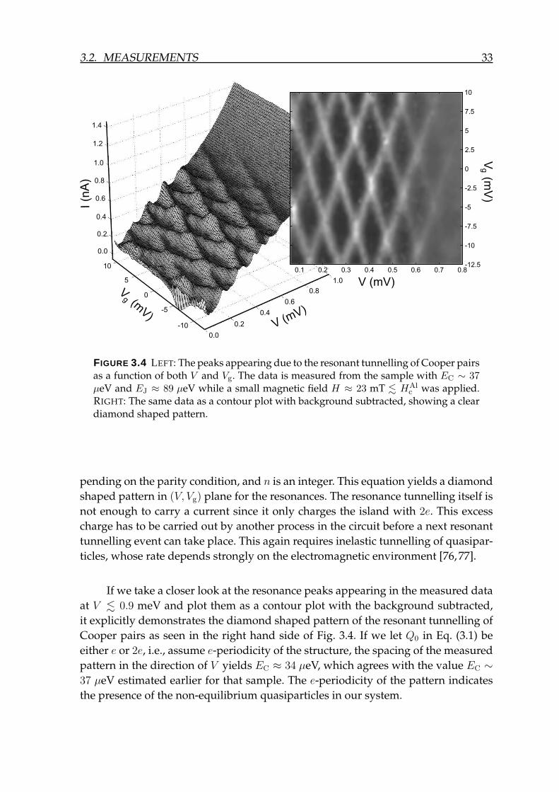
In three of the measured samples there exists clear oscillations in the dI/dV -curvenear the supercurrent as seen in Fig. 3.3. These oscillations are due to gate dependentpeaks as seen in the zoomed I-V curves plotted as a function of both the bias voltageV and the gate voltage Vg in the left hand side of Fig. 3.4. The pattern visible at thebias voltages below V . 0.9 mV has equal spacing in both V and Vg, and appearsat the onset of the superconductivity on the aluminium leads, while decreasing themagnetic field. Furthermore, it was verified that the position of the peaks does notdepend on the value of the gap of the aluminum electrodes, which was tested byapplying an external magnetic field.
The pattern is similar to the one observed usually in the case of so-calledJosephson quasiparticle (JQP) cycles, where a Cooper pair tunnels through one junc-tion and two quasiparticles through another [61], and thus the authors of [44], wheresimilar pattern was observed, claim it to be due to that. However, the pattern isnot due to JQP cycles since the features of it appear only at much higher voltages,∆Nb+∆Al+EC ≤ eV ≤ ∆Nb+∆Al+3EC, which, e.g., for the sample of Fig. 3.3, yields1.72 mV . V . 1.87 mV [33, 101]. To rule out the possibility that these resonanceswould be due to the coupling of the Josephson oscillations to the electromagneticenvironment of the sample, we have fabricated Al-only single junctions and SSET’swith the same design and measured them in the same dilution refrigerator using thesame set-up. The subgap conductances of these samples can be regarded as a spec-tral analysis of the environment, as seen by the sample. The obtained results showedthat mild resonances do exist but only below 0.15 meV. Above this value (and up tothe quasiparticle threshold voltage) the I-V ’s and the conductances were exactlyflat, for all the samples measured. The strong gate dependency in the position of thepeaks, as seen in Fig. 3.4, also proves them not to appear due to resonances in theelectromagnetic environment.
The phenomena explaining these peaks is resonant tunnelling of Cooper pairs.If we consider the simplest and the most probable resonant tunnelling event whereone Cooper pair tunnels onto or off the island through left or right junction inFig. 3.1, we obtain the constraint
12CΣV ± CgVg ±Q0 − e = 0 (3.1)
for the necessary resonant condition in a symmetric SSET [76]. Here − sign corre-sponds to tunnelling through the left junction and + through the right one, Q0 is thecharge on the island before the tunnelling event, i.e., Q0 is n × 2e or n × 2e + e de-
3.2. MEASUREMENTS 33
V (mV)
V(m
V)
g
V (mV)
V(m
V)
g
I (n
A)
1.4
1.2
1.0
1.0
0.6
0.6
0.4
0.4
0.2
0.2
0.0
10
-10
5
-5
0
0.0
0.8
0.8
FIGURE 3.4 LEFT: The peaks appearing due to the resonant tunnelling of Cooper pairsas a function of both V and Vg. The data is measured from the sample with EC ∼ 37µeV and EJ ≈ 89 µeV while a small magnetic field H ≈ 23 mT . HAl
c was applied.RIGHT: The same data as a contour plot with background subtracted, showing a cleardiamond shaped pattern.
pending on the parity condition, and n is an integer. This equation yields a diamondshaped pattern in (V, Vg) plane for the resonances. The resonance tunnelling itself isnot enough to carry a current since it only charges the island with 2e. This excesscharge has to be carried out by another process in the circuit before a next resonanttunnelling event can take place. This again requires inelastic tunnelling of quasipar-ticles, whose rate depends strongly on the electromagnetic environment [76, 77].
If we take a closer look at the resonance peaks appearing in the measured dataat V . 0.9 meV and plot them as a contour plot with the background subtracted,it explicitly demonstrates the diamond shaped pattern of the resonant tunnelling ofCooper pairs as seen in the right hand side of Fig. 3.4. If we let Q0 in Eq. (3.1) beeither e or 2e, i.e., assume e-periodicity of the structure, the spacing of the measuredpattern in the direction of V yields EC ≈ 34 µeV, which agrees with the value EC ∼37 µeV estimated earlier for that sample. The e-periodicity of the pattern indicatesthe presence of the non-equilibrium quasiparticles in our system.
34 3. SUPERCONDUCTING AL/NB/AL SET
3.2.3 q-MQT in superconducting SET
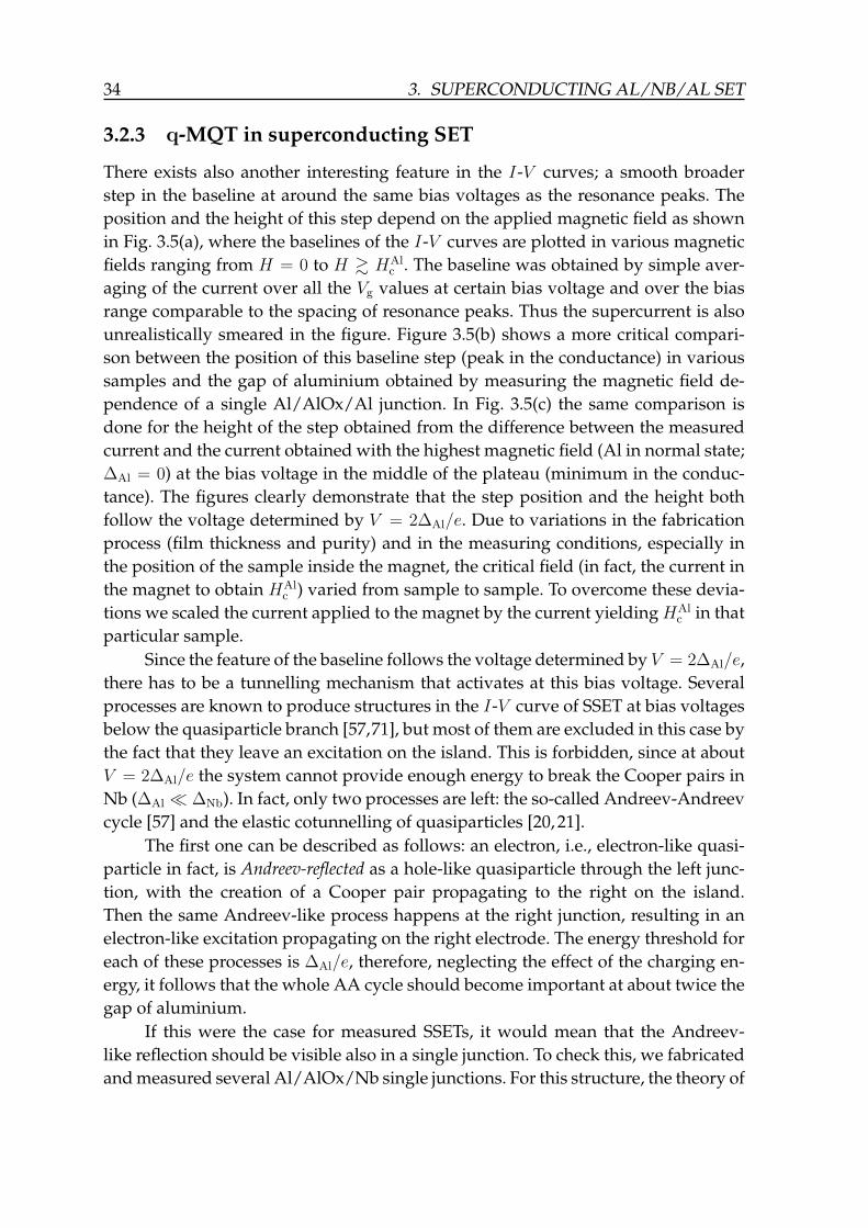
There exists also another interesting feature in the I-V curves; a smooth broaderstep in the baseline at around the same bias voltages as the resonance peaks. Theposition and the height of this step depend on the applied magnetic field as shownin Fig. 3.5(a), where the baselines of the I-V curves are plotted in various magneticfields ranging from H = 0 to H & HAl
c . The baseline was obtained by simple aver-aging of the current over all the Vg values at certain bias voltage and over the biasrange comparable to the spacing of resonance peaks. Thus the supercurrent is alsounrealistically smeared in the figure. Figure 3.5(b) shows a more critical compari-son between the position of this baseline step (peak in the conductance) in varioussamples and the gap of aluminium obtained by measuring the magnetic field de-pendence of a single Al/AlOx/Al junction. In Fig. 3.5(c) the same comparison isdone for the height of the step obtained from the difference between the measuredcurrent and the current obtained with the highest magnetic field (Al in normal state;∆Al = 0) at the bias voltage in the middle of the plateau (minimum in the conduc-tance). The figures clearly demonstrate that the step position and the height bothfollow the voltage determined by V = 2∆Al/e. Due to variations in the fabricationprocess (film thickness and purity) and in the measuring conditions, especially inthe position of the sample inside the magnet, the critical field (in fact, the current inthe magnet to obtain HAl
c ) varied from sample to sample. To overcome these devia-tions we scaled the current applied to the magnet by the current yielding HAl
c in thatparticular sample.
Since the feature of the baseline follows the voltage determined by V = 2∆Al/e,there has to be a tunnelling mechanism that activates at this bias voltage. Severalprocesses are known to produce structures in the I-V curve of SSET at bias voltagesbelow the quasiparticle branch [57,71], but most of them are excluded in this case bythe fact that they leave an excitation on the island. This is forbidden, since at aboutV = 2∆Al/e the system cannot provide enough energy to break the Cooper pairs inNb (∆Al ∆Nb). In fact, only two processes are left: the so-called Andreev-Andreevcycle [57] and the elastic cotunnelling of quasiparticles [20, 21].
The first one can be described as follows: an electron, i.e., electron-like quasi-particle in fact, is Andreev-reflected as a hole-like quasiparticle through the left junc-tion, with the creation of a Cooper pair propagating to the right on the island.Then the same Andreev-like process happens at the right junction, resulting in anelectron-like excitation propagating on the right electrode. The energy threshold foreach of these processes is ∆Al/e, therefore, neglecting the effect of the charging en-ergy, it follows that the whole AA cycle should become important at about twice thegap of aluminium.
If this were the case for measured SSETs, it would mean that the Andreev-like reflection should be visible also in a single junction. To check this, we fabricatedand measured several Al/AlOx/Nb single junctions. For this structure, the theory of
3.2. MEASUREMENTS 35
0.0 0.5 1.00.0
0.1
0.2
DA
l(m
eV
)
0.0 0.5 1.00.0
0.1
0.2
0.3
DA
l(m
eV
)
H/Hc
Al
(a)
(b)
(c)
FIGURE 3.5 (a) Averaged over Vg I-V curves measured at several different magneticfields ranging from H = 0 (highest absolute value of current) to H & HAl
c (lowestabsolute value of current). The baseline was obtained by simple averaging over theresonance peaks. (b) Comparison between the position of this baseline step in varioussamples and the gap of aluminium obtained by measuring the magnetic field depen-dence of a single Al/Al junction. Open circles are the data measured from single Al/Aljunction and other symbols correspond to the data extracted from the I-V curves ofthree different samples. The I-V curves shown in (a) correspond to a sample markedas solid triangles. (c) The gap of the aluminium (circles) and step position (triangle) asin (b), as well as the height of the step (star) as a function of the magnetic field.
multiple Andreev reflection [32,84,103] and multiple-particle tunneling [75,114] pre-dict a conductance peak (corresponding to a step in the current) at ∆Al/e for a singleAndreev reflection. In fact, the general structure predicted by these theories is muchmore complicated, with peaks at 2∆Al/2ne, 2∆Nb/2ne, and (∆Nb + ∆Al)/(2n + 1)e.None of these structures have been observed in our single-junctions. However, someleak currents at various voltages, probably due to other processes that one cannotyet characterize well, were seen. It was carefully checked that the activation voltagefor these processes does not depend on the gap of Al (by sweeping the temperatureup to the critical temperature for Al), therefore, even if they might contribute to thebackground current in the SSET, they cannot account completely for the variation ofthe current with the Al gap.
These measurements of the single junctions also rule out the possibility thatthe baseline feature would be due to the sequential tunnelling through the subgapquasiparticle states in Nb, which are the most probable reason for the smearing ofthe I-V characteristics as discussed before. If the observed baseline step would bedue to these extra quasiparticle states it should be visible also at the single junctionI-V curves [47] and it should show gate modulation with an amplitude comparable
36 3. SUPERCONDUCTING AL/NB/AL SET
2DAl
2DAl
2DNb
Al AlII Nb
eV
EC
-e
FIGURE 3.6 Schematic view of the elastic cotunnelling of an electron-like quasiparti-cle from the left electrode (below the gap of Al) to the right electrode (above the gapof Al), via a virtual excitation on the island with energy Eex > ∆Nb. The effective andthe virtual processes are shown by thick arrows. The vertical axis is the energy andthe horizontal is the density of the electron states in the two Al electrodes. Dashedlines show the Fermi energy of the corresponding electrode or island and the dottedlines correspond to the Coulomb states in the island due to the charging energy EC.It is clearly seen that the threshold voltage for the cotunnelling event to happen iseV = 2∆Al. Since EC ∆Nb the effect of the charging energy and thus the effect ofthe gate voltage is negligible.
to the modulation due to the resonant tunnelling of Cooper pairs. The lack of thisfeature in the single junction measurements and the lack of the gate modulationproves that this is not the case.
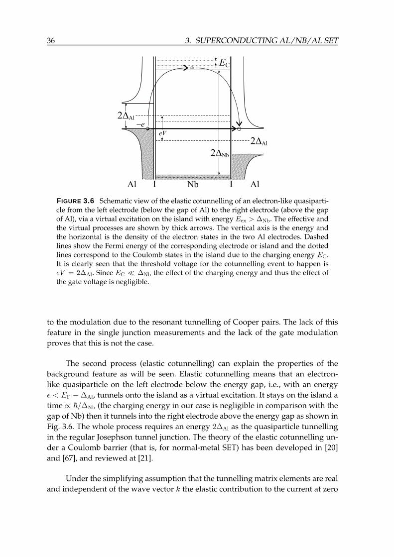
The second process (elastic cotunnelling) can explain the properties of thebackground feature as will be seen. Elastic cotunnelling means that an electron-like quasiparticle on the left electrode below the energy gap, i.e., with an energyε < EF −∆Al, tunnels onto the island as a virtual excitation. It stays on the island atime ∝ ~/∆Nb (the charging energy in our case is negligible in comparison with thegap of Nb) then it tunnels into the right electrode above the energy gap as shown inFig. 3.6. The whole process requires an energy 2∆Al as the quasiparticle tunnellingin the regular Josephson tunnel junction. The theory of the elastic cotunnelling un-der a Coulomb barrier (that is, for normal-metal SET) has been developed in [20]and [67], and reviewed at [21].
Under the simplifying assumption that the tunnelling matrix elements are realand independent of the wave vector k the elastic contribution to the current at zero
3.2. MEASUREMENTS 37
temperature reads1:
Iel =1
eReff
∞∫∆Al
dEL
∞∫∆Al
dERELER√
E2L −∆2
Al
√E2
R −∆2Al
T 2eff(EL, ER)δ(eV − EL − ER), (3.2)
where Reff = RT,1RT,2/RK, RT,1 and RT,2 are the resistances of the two junctions,and
Teff(EL, ER) = 2π
∞∫∆Nb
dEE√
E2 −∆2Nb
[1
E1 + E − EL
− 1
E2 − E + ER
](3.3)
where E1 and E2 are defined in [20].One can readily see that the first formula is analog to the quasiparticle tun-
nelling current between two Al superconductors
Iqp =1
eRT
∞∫∆Al
dEL
∞∫∆Al
dERELER√
E2L −∆2
Al
√E2
R −∆2Al
δ(eV − EL − ER), (3.4)
with an effective junction resistance RT → Reff and with an energy-dependent nor-malised tunnelling matrix element Teff , describing the barrier formed by ∆Nb. Usu-ally it is assumed that |T |2 is energy-independent and is included in the definitionof RT. Also it shows that the elastic current starts at 2∆Al and the corresponding I-Vfeature will be step-like with the height proportional to the ∆Al, as in the regularJosephson tunnel junction. In the limit of charging energy and bias voltages muchsmaller then the Nb gap, these equations indicate that Teff is in fact independentof the energies E1 and E2. Therefore, one expects a gate voltage insensitivity of thebackground. All these predicted features agree with the measurements as seen inFig. 3.5 for the ∆Al proportionality and in Fig. 3.4 for the gate insensitivity.
In a normal-metal SET the inelastic cotunnelling usually dominates over theelastic one, which is due to the fact ε EC, where ε is the spacing of the singleelectron states in the metal [18, 20]. Since any excitation with an excess electron inthe island is now exponentially suppressed Iinel ∝ e−D(T )/kBT at low temperatures,the inelastic cotunnelling (which always leaves the excitation on the island) is sig-nificantly reduced. Here D(T ) is given by Eq. (2.7) with ∆Nb. Also one might quali-tatively interprete the lowest excitation energy of the island ∆Nb EC as a spacingof the single electron states in the vicinity of the Fermi surface. This indicates theelastic cotunnelling being the dominant process.
1A better theory should be supplemented with a description of the diffusion of the electron insidethe island as in [20, 21].

38 3. SUPERCONDUCTING AL/NB/AL SET
4 Decoherence in circuits of smallJosephson junctions
4.1 Quantum computing
As mentioned already at the very beginning of this thesis, the rapid progress in thefield of microelectronics during the past years and the strong effort to miniaturiseany circuit have pushed the size of the electrical devices down steadily. This has,among other things, forced the information and computing science to reconsiderits historical connection to classical physics, and expand the insight to include alsoquantum mechanics as a part of information theory. This has led to the emergenceof a new field of quantum computing in 1980’s and it has undergone a rapid develop-ment in 1990’s.
Quantum computing connects the information theory very tightly to its phys-ical realisation. From that point of view, it is no longer reasonable to talk about ab-stract information, but rather one has to always take into account the physical sys-tem the information is coded in. This means that information is part of the systemand the amount of it affects the entropy of the whole system. Furthermore, this alsoyields that wasting of information costs energy, which was the key to the answer ofthe famous old thermodynamic paradox called Maxwell’s Demon.
4.1.1 Qubit
Classical information is formed of bits, whereas quantum information is formedof quantum bits, so-called qubits. A classical bit can have a value 0 or 1, which isdetermined by a threshold property of a macroscopic system, e.g., voltage below orabove 2.5 V. Thus, a register of n bits can have any of the 2n values between 000 . . . 0
and 111 . . . 1. The qubit is usually presented and stored in a microscopic system, e.g.,the electron or photon, where some definite and distinguished quantum mechanicalstates, |Ψ〉i, represent the classical states 0 and 1 and form a basis. For example,the spin of an electron has the definite states |↓ 〉 ≡ 0 and |↑ 〉 ≡ 1 in magnetic field.
Unlike a classical bit, a qubit can also have any superposition of 0 and 1 asits value, e.g.,
√1/2(|0〉 ± |1〉). Nevertheless, this does not mean the same as fuzzy
logic, in which a classical bit is allowed to have any value between 0 and 1, but qubitcontains also the quantum mechanical phase. For example, the state
√1/2(|0〉+ i|1〉)
39
40 4. DECOHERENCE IN CIRCUITS OF SMALL JOSEPHSON JUNCTIONS
is different from the states above. In general the state of the register with n qubitscan be written in the form
|Ψ〉 =11...1∑
x=00...0
cx|x〉, (4.1)
where cx are complex numbers satisfying the relation∑
x |cx|2 = 1. Thus the registercan simultaneously contain all the 2n classical states in a superposition.
When measuring the state of the qubit it ‘collapses’, however, to either of thebasis states so that the general state |Ψ〉 = α|0〉+ β|1〉 gives an answer 0 with proba-bility of |α|2 and 1 with probability |β|2. Anyway, the basis of the qubit does not needto be fixed during the operations and we can perform measurement of the state aswell using, e.g., the basis of |±〉 =
√1/2(|0〉 ± |1〉). The same general state as above
reads in this basis |Ψ〉 =√
1/2[(α + β)|+〉 − (α − β)|−〉], and the result is |+〉 withprobability |α+ β|2/2 and |−〉 with probability |α− β|2/2.
Another important difference between a qubit and a classical bit is that an un-known state of a quantum bit cannot be fully copied. This principle is a consequence ofthe nature of quantum mechanics and was proven by Wootters and Zurek, and byDieks in 1982 [42, 132]. It prevents the use of regular classical error correction algo-rithms in qubits, since they always involve copying of the original bit, and it alsoprevents one to get around the principle of destructive measurement.
4.1.2 Entanglement
A general state of the register with n qubits (4.1) naturally contains all the combina-tions of the single qubit states, e.g., in the register of two qubits a state
√1/2(|00〉+
|01〉) = |0〉 ⊗√
1/2(|0〉 + |1〉), but it also contains the states like√
1/2(|00〉 + |11〉),which cannot be expressed as a tensor product of the two single qubit states. Itmeans that neither of the two qubits has a definite state of its own even if the systemof these two qubits has a definite state [26]. This kind of states are called entangled. Inthe case of n qubits most of the states are entangled and the true power of quantumcomputing is based on the manipulation of the states like this.
The state√
1/2(|00〉+|11〉) mentioned above is the so-called EPR-state (Einstein-Podolsky-Rosen) and it has a maximal entanglement between the two qubits. Thisstate can be used, e.g., to produce superdense coding [26] or quantum teleportation[24, 26]. In both of these phenomena the EPR-pair is split between the sender andthe receiver so that the entanglement is not disturbed. For example quantum tele-portation, in which an unknown quantum state is transferred far away, is achievednow by only sending two bits of classical data, e.g., by phone. Yet, this does notviolate the rule of denied copying.
4.1. QUANTUM COMPUTING 41
4.1.3 Gates and quantum parallelism
Classic computing is done using elementary logical gates. The output of a classiclogical gate is usually one bit, whereas more than one input bit is often needed,e.g., in the AND-gate (2 bits7→1 bit) : (11) → 1; (01), (10), (00) → 0. The outputcan also include more than one bit, but almost all the time the number of input bitsis larger than of output bits. Thus, this computing is irreversible and energy is lostduring computation since every gate operation reduces the number of bits and sothe total amount of information in the system is reduced. In quantum computing itis essential to preserve all the quantum mechanical properties of the state such asentanglement. Thus, the gates used in quantum computing are unitary transforma-tions, which reversibly operate to the state vectors without losing any information.This also makes it possible to use tiny systems in computing, since there is almostno energy lost during the computation that would easily heat the small structures.
There are only three ‘Basis’ gates needed to form any gate in quantum com-puting. The usual choice for this basis consists of the phase shift gate:
Φ(ϕ) =
(1 0
0 eiϕ
), (4.2)
which can change the phase of the state, e.g., Φ(ϕ)(α|0〉 + β|1〉) = α|0〉 + βeiϕ|1〉.Another gate needed is the Hadamard gate
H =1√2
(1 1
1 −1
), (4.3)
which can be used in creation of superposition states needed as an initial state inmany computation algorithms, e.g., 23/2H1H2H3|000〉 = |000〉 + |001〉 + |010〉 + · · · +|110〉 + |111〉. Both these gates are single qubit gates operating on one qubit. In ad-dition, to form a full basis one needs a two gubit gate C-NOT (Controlled NOT)
C =
1 0 0 0
0 1 0 0
0 0 0 1
0 0 1 0
: C|y〉|x〉 = |y ⊕ x〉|x〉, (4.4)
where |x〉 and |y〉 are any states of kind α|0〉 + β|1〉, and y ⊕ x means, in the case ofclassic logical states, that y is flipped if x = 1.
As mentioned above the register of qubits can simultaneously contain all thepossible classical combinations as one superposition. Using this kind of a state asan initial state of the computation procedure one can simultaneously obtain the re-sults corresponding to all the initial conditions by single computation. This is calleda massive quantum parallelism. Nevertheless, making use of it is not as simple as it
42 4. DECOHERENCE IN CIRCUITS OF SMALL JOSEPHSON JUNCTIONS
sounds. Even the resulting state obtained by the parallel calculation contains all theanswers corresponding to the different initial conditions, the measurement of this fi-nal state gives out only one result, which is chosen along the probability distributiondetermined by the multipliers in the superposition. Thus, to track out all the resultsand their probabilities one has to repeat the calculation at least as many times asthere are different initial conditions and usually much more. This same amount ofcalculation would have been needed in solving the problem using classical compu-tation and hence all the advantages of quantum parallelism have been lost. There-fore, it is essential to develop good computation algorithms, specially designed forthe quantum computing, which can make use of all the advantages of quantum par-allelism. The most famous quantum algorithms are encryption and cryptographyalgorithms [26, 120], the searching algorithm of Grover [70] and the Shor’s factori-sation algorithm that can be used to quickly decode the encryption methods usednowadays [118].
4.1.4 Realisation and decoherence
In principle, any quantum mechanical system, which can exist in any superpositionof two basis states, can serve as a qubit. However, in realisation of such a device onehas to take into account also the requirement that the system needs to be decoupledfrom the rest of the universe. That is the only way to preserve all the quantum me-chanical information in the system. Any coupling, e.g., measurement, to the outsideworld would induce a growing entanglement between the system states and thestates of the outside world. This process means that at the end the system does nothave a state of its own, and the quantum coherence has been shared with the outsideworld, which makes the system behave as a classical statistical mixture instead of apure quantum mechanical state with a definite phase.
This process is called decoherence and the stronger the coupling to the outsideworld is, the faster it is. This is why everyday physical systems behave classically[136]. In any macroscopic object the contact to the outside world is so strong thatdecoherence happens in a time scale too fast to perceive and we observe only clas-sical behaviour of the system. We can also think that the outside world is constantlymeasuring the system and thus the wave vector of the (sub)system ‘collapses’. Thedecoherence is one of the biggest problems in realisation of solid state qubits.
4.1.5 Squbit
The most obvious representation of a qubit would be any spin-1/2 particle, e.g.,an electron, or a photon with two different polarisations. These options have beenwidely studied and in some experiments the qubit, which can be manipulated withlasers, has been successfully constructed using atoms or ions [25, 49, 50]. Also the
4.2. DECOHERENCE IN SUPERCONDUCTING NANOSTRUCTURES 43
photon excitations in a microwave cavity have operated as a qubit and the entan-glement between two qubits of this kind has been experimentally demonstrated[73, 127].
The major disadvantage of the qubits above is that scalability is very ques-tionable. It would be extremely difficult to increase the number of connected orinteracting qubits in any of these systems. Thus, the suggestions to use supercon-ducting nanostructures as a qubit, to be called squbit in what follows [14, 30, 31, 95,96, 108, 116, 117], have gained lots of interest due to their relatively easy scalabil-ity and expandability to structures involving several squbits or even squbit net-works. There have been several experiments in which the operation of a squbithas been successfully demonstrated in practice, with promisingly long decoherencetimes [4, 15, 28, 35, 36, 52] potentially allowing quantum manipulations and applica-tion of specially developed error correction codes [35, 59, 102, 128, 131].
The principle of the squbit is based on the possible superposition of the chargestates in the CPB [96] or in the arrays of Josephson junctions [14] (charge squbit), oron the superposition of supercurrents flowing in two different directions in SQUIDS(Superconducting quantum interference device) [108] (flux squbit). The simplest squ-bit is the CPB where the basis states can be chosen to be |0〉 and |1〉, with zero orone Cooper pairs on the island, respectively. As explained in Ch. 2.3, the Josephsoncoupling induces the new eigenstates of the system, which are superpositions ofthese charge states as shown in Fig. 2.5. The CPB can now be operated as a squbitby using only the ground state and the gate voltage to manipulate the multipliers inthe superposition state.
4.2 Decoherence in superconducting nanostructures
4.2.1 ‘P(E)’-Theory
As described in the previous chapter decoherence is the most limiting phenomenonin realising a squbit, and it arises due to a coupling to the outside world. In case ofJosephson junctions one of the major sources of decoherence is the electromagneticenvironment in the vicinity of the sample. In most cases it is strongly coupled tothe system under study and can have a significant effect on the behaviour of thecircuit [1, 53, 77]. Fortunately, it is a controllable source of decoherence, unlike, e.g.,random motion of background charges near the sample.
There exists a well developed theory of the electromagnetic environment andhow it affects the tunnelling in small tunnel junctions [1, 69, 77, 125]. Here only theresults for a superconducting Josephson junction are presented. The environmentis modelled as an infinite number of harmonic LC-oscillators, which can representan arbitrary environment as explained in [34]. The dissipation in the system understudy arises from the coupling of the degrees of freedom, i.e.,Q and ϕ, to the degrees
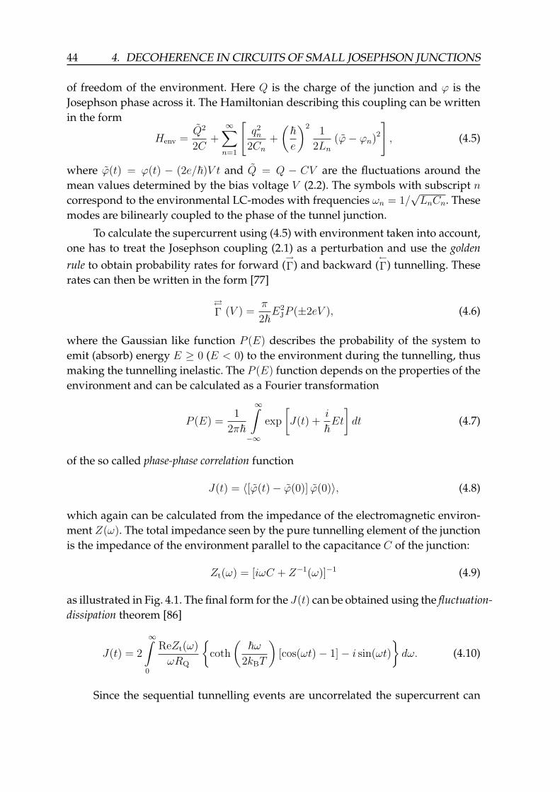
44 4. DECOHERENCE IN CIRCUITS OF SMALL JOSEPHSON JUNCTIONS
of freedom of the environment. Here Q is the charge of the junction and ϕ is theJosephson phase across it. The Hamiltonian describing this coupling can be writtenin the form
Henv =Q2
2C+∞∑
n=1
[q2n
2Cn
+
(~e
)21
2Ln
(ϕ− ϕn)2
], (4.5)
where ϕ(t) = ϕ(t) − (2e/~)V t and Q = Q − CV are the fluctuations around themean values determined by the bias voltage V (2.2). The symbols with subscript ncorrespond to the environmental LC-modes with frequencies ωn = 1/
√LnCn. These
modes are bilinearly coupled to the phase of the tunnel junction.
To calculate the supercurrent using (4.5) with environment taken into account,one has to treat the Josephson coupling (2.1) as a perturbation and use the goldenrule to obtain probability rates for forward (
→Γ) and backward (
←Γ) tunnelling. These
rates can then be written in the form [77]
Γ (V ) =
π
2~E2
JP (±2eV ), (4.6)
where the Gaussian like function P (E) describes the probability of the system toemit (absorb) energy E ≥ 0 (E < 0) to the environment during the tunnelling, thusmaking the tunnelling inelastic. The P (E) function depends on the properties of theenvironment and can be calculated as a Fourier transformation
P (E) =1
2π~
∞∫−∞
exp
[J(t) +
i
~Et
]dt (4.7)
of the so called phase-phase correlation function
J(t) = 〈[ϕ(t)− ϕ(0)] ϕ(0)〉, (4.8)
which again can be calculated from the impedance of the electromagnetic environ-ment Z(ω). The total impedance seen by the pure tunnelling element of the junctionis the impedance of the environment parallel to the capacitance C of the junction:
Zt(ω) = [iωC + Z−1(ω)]−1 (4.9)
as illustrated in Fig. 4.1. The final form for the J(t) can be obtained using the fluctuation-dissipation theorem [86]
J(t) = 2
∞∫0
ReZt(ω)
ωRQ
coth
(~ω
2kBT
)[cos(ωt)− 1]− i sin(ωt)
dω. (4.10)
Since the sequential tunnelling events are uncorrelated the supercurrent can
4.2. DECOHERENCE IN SUPERCONDUCTING NANOSTRUCTURES 45
Z (w)
V
R CT
Z (w)t
V
RT
Z (w)
V
RT
C
FIGURE 4.1 Description of the total external impedance seen by the pure tunnellingelement of the Josephson junction. The total impedance is of the form Zt(ω) =[iωC + Z−1(ω)]−1
be calculated as a difference between the opposite tunnelling rates, which yields
IS = 2e[→Γ (V )−
←Γ (V )
]=πeE2
J
~[P (2eV )− P (−2eV )] . (4.11)
The P (E) obeys the so-called detailed balance relation P (−E) = P (E) exp[−E/(kBT )],which indicates that at the low temperatures P (E) is peaked around a positive Enear zero. Thus, (4.11) represents the two antisymmetric peaks around the zero volt-age, with the property I(V = 0) = 0. This is the usual shape of the supercurrent ob-served in experiments (see, e.g., Fig. 2.4). The smaller the environment impedanceZ(ω) is, the sharper the peaks are, and more closer to zero bias they are located. Onthe limit of high environment Z(ω) RQ the peaks are broad and centered aroundthe bias corresponding to the charging energy V = ±EC/e.
4.2.2 Decoherence due to electromagnetic environment
In small Josephson junctions the decoherence is closely related to dephasing, whichmeans that the initially well defined Josephson phase ϕ across the junction becomesmore and more arbitrary. This process is best characterised by the quantity 〈[ϕ(t) −ϕ(0)]2〉 = 〈(∆ϕ)2〉, the deviation of the phase fluctuations from their value at t = 0.In charge squbits the phase needs to be fixed and thus the bias voltage has to bezero. Due to that, ϕ = ϕ − (2e/~)V t = ϕ and the phase-phase correlation functionJ(t) relates directly the Josephson phases at different times. This connection cannow be used to relate the quantity 〈(∆ϕ)2〉 to the electromagnetic environment [4].Using 〈ϕ(t)2〉 = 〈ϕ(0)2〉, which is a consequence of the stationarity of equilibriumcorrelation functions, one can write
〈∆ϕ2〉 = 〈ϕ(t)2〉 − 〈ϕ(0)ϕ(t)〉 − 〈ϕ(t)ϕ(0)〉+ 〈ϕ(0)2〉= −〈ϕ(0)[ϕ(t)− ϕ(0)]〉 − 〈[ϕ(t)− ϕ(0)]ϕ(0)〉. (4.12)
46 4. DECOHERENCE IN CIRCUITS OF SMALL JOSEPHSON JUNCTIONS
Now using the fact that ϕ(t) is hermitian one obtains
〈(∆ϕ)2〉 = −2ReJ(t), (4.13)
which directly relates the dephasing to the electromagnetic environment via phase-phase correlation function J(t). One can also show that the decoherence rate is re-lated to the same quantity [5]. To simplify the calculations, we do this only in thecase of a CPB and with the basis of |n〉 = |0〉, |1〉.
First, we have to split the Hamiltonian (4.5) to the energy of the pure envi-ronment Henv =
∑j ~ωj(b
†jbj + 1/2) and to the Hamiltonian, Hint, describing the
interaction between the junction and its environment. Here b†j and bj are the creationand annihilation operators of the bosonic environmental modes j with energy ~ωj ,respectively. The total Hamiltonian reads now
H = Hch +HJ +Henv +Hint, (4.14)
and the total wavefunction Ψ is a tensor product of the charge state |n〉 and the stateof the environment |~k〉: Ψ = |n〉 ⊗ |~k〉, where n is the number of Cooper pairs inthe island and ~k = (k1, k2, · · · ) is the configuration of environmental modes withoccupation numbers kj . We can now write the density matrix ρ~k in the given basis as
ρ~k =: ρ⊗ |~k〉 = ΨΨ† ⊗ |~k〉 =
(a1
a2
)(a∗1a
∗2)⊗ |~k〉
=
(|a1|2 a1a
∗2
a2a∗1 |a2|2
)⊗ |~k〉 :=
(ρ
~k11 ρ
~k12
ρ~k21 ρ
~k22
). (4.15)
In the density matrix the nondiagonal elements are directly related to the coherenceof the state. If these so-called coherence elements are of the form aia
∗j as shown in
(4.15) the state is a pure quantum mechanical state. On the contrary if these elementsvanish the density matrix has to be presented as a sum of different states and itrepresents a classical statistical mixture. Thus the effect of decoherence is to reducethese elements until they vanish.
Now the Hamiltonian describing the interaction between the CPB and the en-vironment can be written in this basis as [34]
Hint = −i√π∑
j
~ωj
√Zj
RQ
(bj − b†j
)0
0 −(bj − b†j
) , (4.16)
where Zj is the impedance of the mode j. In the interaction picture one can write:H = H0 +V , where H0 = HCh +HJ +Henv and V = Hint [37]. In this picture the state
4.2. DECOHERENCE IN SUPERCONDUCTING NANOSTRUCTURES 47
vectors are given by ΨI(t) = eiH0t/~Ψ(t) and
VI(t)=eiH0t/~V e−iH0t/~
=−i√π∑
j
~ωj
√Zj
RQ
(eiH0t/~bje
−iH0t/~ − eiH0t/~b†je−iH0t/~
)(1 0
0 −1
)
=−i√π∑
j
~ωj
√Zj
RQ
(e
i∑k
b†kbkωktbje−i
∑k
b†kbkωkt− e
i∑k
b†kbkωktb†je−i
∑k
b†kbkωkt)(
1 0
0 −1
)
=−i√π∑
j
~ωj
√Zj
RQ
(bje−iωjt − b†je
iωjt)
0
0 −(bje−iωjt − b†je
iωjt) .
In the last step the commutation rule [bi, b†j] = δij was used. The equation of motion
for ρ~kI := ρ
~k (for simplicity) is given by the Liouville equation:
i~dρ
~k(t)
dt=[VI, ρ
~k(t)]. (4.17)
For the commutator [VI(t), ρ~k(t)] we obtain
[VI(t), ρ~k(t)] = −2i
√π∑
j
~ωj
√Zj
RQ
(bje−iωjt − b†je
iωjt)( 0 ρ
~k12
−ρ~k21 0
),
which yields the differential equation for the coherence matrix elements ρ~k12(t) =
ρ~k∗21(t)
i~dρ
~k12(t)
dt= −2i
√π∑
j
~ωj
√Zj
RQ
(bje−iωjt − b†je
iωjt)ρ
~k12(t).
By integrating the differential equation from t = 0 to t we obtain
ρ~k12(t)
ρ~k12(0)
=∏
j
exp
−2i
√π
√Zj
RQ
[bj(1− e−iωjt
)+ b†j
(1− eiωjt
)].
Next we have to trace out the environmental configurations ~k. This can be doneusing the relation
∑~k ρ
~kij = ρij and applying the Glauber formula for non-zero tem-
perature [66]:
⟨exp
[γ(νb+ ν∗b†
)]⟩= exp
[−1
2|ν|2 coth
(~ω
2kBT
)γ2
]. (4.18)
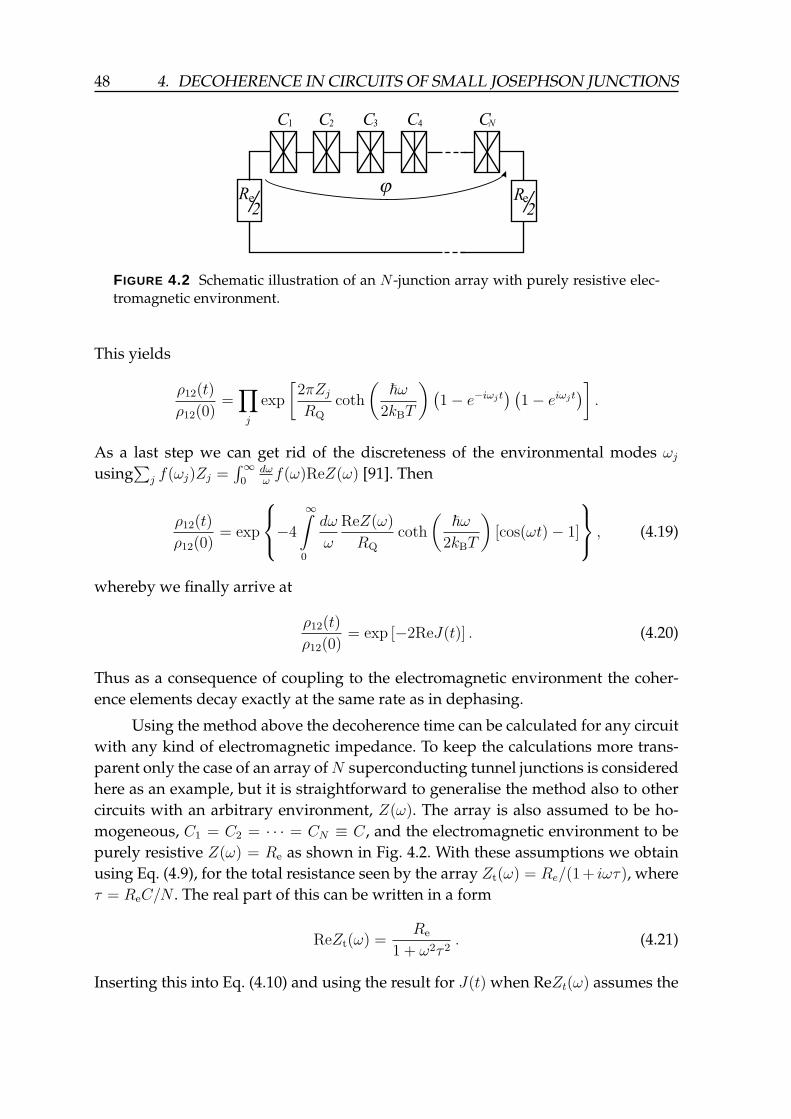
48 4. DECOHERENCE IN CIRCUITS OF SMALL JOSEPHSON JUNCTIONS
e e
FIGURE 4.2 Schematic illustration of an N -junction array with purely resistive elec-tromagnetic environment.
This yields
ρ12(t)
ρ12(0)=∏
j
exp
[2πZj
RQ
coth
(~ω
2kBT
)(1− e−iωjt
) (1− eiωjt
)].
As a last step we can get rid of the discreteness of the environmental modes ωj
using∑
j f(ωj)Zj =∫∞
0dωωf(ω)ReZ(ω) [91]. Then
ρ12(t)
ρ12(0)= exp
−4
∞∫0
dω
ω
ReZ(ω)
RQ
coth
(~ω
2kBT
)[cos(ωt)− 1]
, (4.19)
whereby we finally arrive at
ρ12(t)
ρ12(0)= exp [−2ReJ(t)] . (4.20)
Thus as a consequence of coupling to the electromagnetic environment the coher-ence elements decay exactly at the same rate as in dephasing.
Using the method above the decoherence time can be calculated for any circuitwith any kind of electromagnetic impedance. To keep the calculations more trans-parent only the case of an array ofN superconducting tunnel junctions is consideredhere as an example, but it is straightforward to generalise the method also to othercircuits with an arbitrary environment, Z(ω). The array is also assumed to be ho-mogeneous, C1 = C2 = · · · = CN ≡ C, and the electromagnetic environment to bepurely resistive Z(ω) = Re as shown in Fig. 4.2. With these assumptions we obtainusing Eq. (4.9), for the total resistance seen by the array Zt(ω) = Re/(1+ iωτ), whereτ = ReC/N . The real part of this can be written in a form
ReZt(ω) =Re
1 + ω2τ 2. (4.21)
Inserting this into Eq. (4.10) and using the result for J(t) when ReZt(ω) assumes the
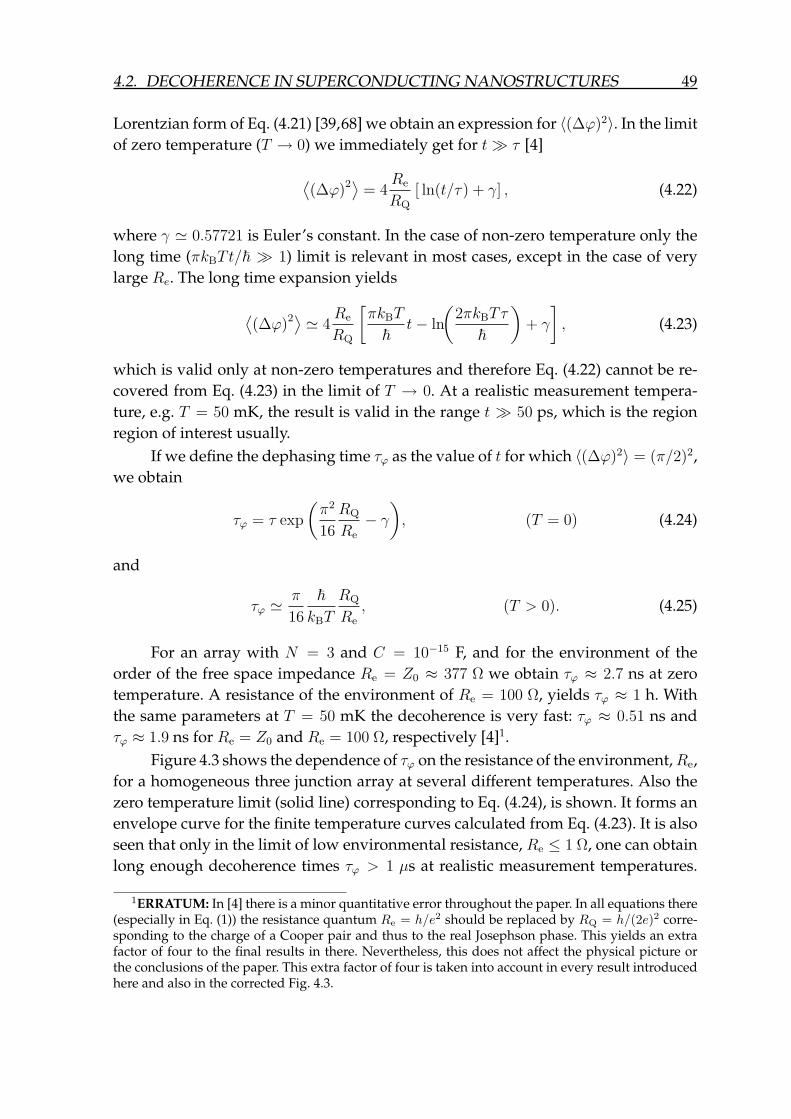
4.2. DECOHERENCE IN SUPERCONDUCTING NANOSTRUCTURES 49
Lorentzian form of Eq. (4.21) [39,68] we obtain an expression for 〈(∆ϕ)2〉. In the limitof zero temperature (T → 0) we immediately get for t τ [4]
⟨(∆ϕ)2⟩ = 4
Re
RQ
[ ln(t/τ) + γ] , (4.22)
where γ ' 0.57721 is Euler’s constant. In the case of non-zero temperature only thelong time (πkBTt/~ 1) limit is relevant in most cases, except in the case of verylarge Re. The long time expansion yields
⟨(∆ϕ)2⟩ ' 4
Re
RQ
[πkBT
~t− ln
(2πkBTτ
~
)+ γ
], (4.23)
which is valid only at non-zero temperatures and therefore Eq. (4.22) cannot be re-covered from Eq. (4.23) in the limit of T → 0. At a realistic measurement tempera-ture, e.g. T = 50 mK, the result is valid in the range t 50 ps, which is the regionregion of interest usually.
If we define the dephasing time τϕ as the value of t for which 〈(∆ϕ)2〉 = (π/2)2,we obtain
τϕ = τ exp
(π2
16
RQ
Re
− γ
), (T = 0) (4.24)
and
τϕ 'π
16
~kBT
RQ
Re
, (T > 0). (4.25)
For an array with N = 3 and C = 10−15 F, and for the environment of theorder of the free space impedance Re = Z0 ≈ 377 Ω we obtain τϕ ≈ 2.7 ns at zerotemperature. A resistance of the environment of Re = 100 Ω, yields τϕ ≈ 1 h. Withthe same parameters at T = 50 mK the decoherence is very fast: τϕ ≈ 0.51 ns andτϕ ≈ 1.9 ns for Re = Z0 and Re = 100 Ω, respectively [4]1.
Figure 4.3 shows the dependence of τϕ on the resistance of the environment,Re,for a homogeneous three junction array at several different temperatures. Also thezero temperature limit (solid line) corresponding to Eq. (4.24), is shown. It forms anenvelope curve for the finite temperature curves calculated from Eq. (4.23). It is alsoseen that only in the limit of low environmental resistance, Re ≤ 1 Ω, one can obtainlong enough decoherence times τϕ > 1 µs at realistic measurement temperatures.
1ERRATUM: In [4] there is a minor quantitative error throughout the paper. In all equations there(especially in Eq. (1)) the resistance quantum Re = h/e2 should be replaced by RQ = h/(2e)2 corre-sponding to the charge of a Cooper pair and thus to the real Josephson phase. This yields an extrafactor of four to the final results in there. Nevertheless, this does not affect the physical picture orthe conclusions of the paper. This extra factor of four is taken into account in every result introducedhere and also in the corrected Fig. 4.3.
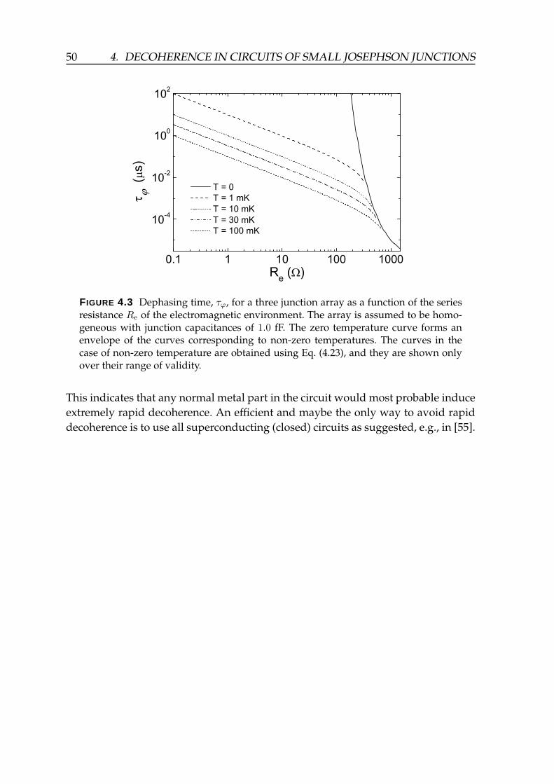
50 4. DECOHERENCE IN CIRCUITS OF SMALL JOSEPHSON JUNCTIONS
FIGURE 4.3 Dephasing time, τϕ, for a three junction array as a function of the seriesresistance Re of the electromagnetic environment. The array is assumed to be homo-geneous with junction capacitances of 1.0 fF. The zero temperature curve forms anenvelope of the curves corresponding to non-zero temperatures. The curves in thecase of non-zero temperature are obtained using Eq. (4.23), and they are shown onlyover their range of validity.
This indicates that any normal metal part in the circuit would most probable induceextremely rapid decoherence. An efficient and maybe the only way to avoid rapiddecoherence is to use all superconducting (closed) circuits as suggested, e.g., in [55].
5 Cooper pair pump
The Cooper pair pump (CPP) consists of three or more mesoscopic Josephson junc-tions in series with gate voltages capacitively coupled to each of the islands in be-tween. It is in focus due to the many studies carried out concerning the parametricpumping of charge, an idea originally introduced by Thouless in 1982 [122]. Thisphenomenon is based on the ability of a propagating potential well to carry a chargeq through a system. This again makes controlled pumping possible, by periodicallychanging the system parameters at a frequency f to induce propagation of chargeduring every cycle. This yields a DC-current I = qf through the system.
The parametric pumping of charge can be obtained in many different kindsof devices, but most of the attention has been directed towards systems where thecharge q passed through during each cycle is quantised at a certain number ofelectrons, q = ne, where n is an integer. This can be realised, e.g., by semicon-ductor quantum dots by varying the height of the tunnelling barriers [85] or byone-dimensional ballistic channels in a so-called SAW-pump, where the transportis induced by a surface acoustoelectric wave (SAW) [115, 121]. The most promis-ing candidate so far is the so-called single electron pump consisting of an arrayof three or more mesoscopic metallic tunnel junctions in the Coulomb blockaderegime [81, 82, 111]. Due to the Coulomb blockade the number of electrons in theislands of the array is very accurate and the pumping can be induced by phase-shifted gate voltages, yielding a current I = nef . Here f is the frequency of the RF-signal applied to the gates and the integer number n depends on the amplitude ofthe operating trajectory in the gate variables. These devices are more accurate thanthose based on semiconductors and they are able to provide high precision, evensufficient for metrological applications [81, 82]. Due to its high accuracy the singleelectron pump has been proposed to close the metrological triangle by providingthe standard for electrical current [74, 81, 82, 92].
The only drawback in the single electron pump is the low operating frequencyf . 5 MHz, which cannot provide high enough current for metrological applica-tions. At higher frequencies the accuracy is lost due to coherent higher order chargetransfer processes known as (in)elastic co-tunneling [18, 20, 63] and other sources oferror discussed in [19], [58], [78] and [97]. The maximum operating frequency couldpossibly be pushed higher by using a Cooper pair pump (CPP). The pumping in theCPP is achieved similarly by the gate voltages and the charge is quantised at dis-crete numbers of Cooper pairs in the islands yielding a current I = n2ef . Due to the
51
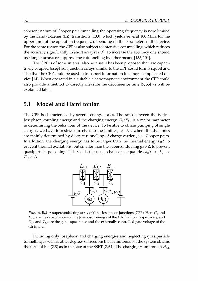
52 5. COOPER PAIR PUMP
coherent nature of Cooper pair tunnelling the operating frequency is now limitedby the Landau-Zener (LZ) transitions [133], which yields several 100 MHz for theupper limit of the operation frequency, depending on the parameters of the device.For the same reason the CPP is also subject to intensive cotunnelling, which reducesthe accuracy significantly in short arrays [2, 3]. To increase the accuracy one shoulduse longer arrays or suppress the cotunnelling by other means [135, 104].
The CPP is of some interest also because it has been proposed that two capaci-tively coupled Josephson junction arrays similar to the CPP could form a squbit andalso that the CPP could be used to transport information in a more complicated de-vice [14]. When operated in a suitable electromagnetic environment the CPP couldalso provide a method to directly measure the decoherence time [5, 55] as will beexplained later.
5.1 Model and Hamiltonian
The CPP is characterised by several energy scales. The ratio between the typicalJosephson coupling energy and the charging energy, EJ/EC, is a major parameterin determining the behaviour of the device. To be able to obtain pumping of singlecharges, we have to restrict ourselves to the limit EJ EC, where the dynamicsare mainly determined by discrete tunnelling of charge carriers, i.e., Cooper pairs.In addition, the charging energy has to be larger than the thermal energy kBT toprevent thermal excitations, but smaller than the superconducting gap ∆ to preventquasiparticle poisoning. This yields the usual chain of inequalities kBT < EJ EC < ∆.
FIGURE 5.1 A superconducting array of three Josephson junctions (CPP). Here Ck andEJ,k are the capacitance and the Josephson energy of the kth junction, respectively, andCg,i and Vg,i are the gate capacitance and the externally controlled gate voltage of theith island.
Including only Josephson and charging energies and neglecting quasiparticletunnelling as well as other degrees of freedom the Hamiltonian of the system obtainsthe form of Eq. (2.8) as in the case of the SSET [2,64]. The charging Hamiltonian HCh
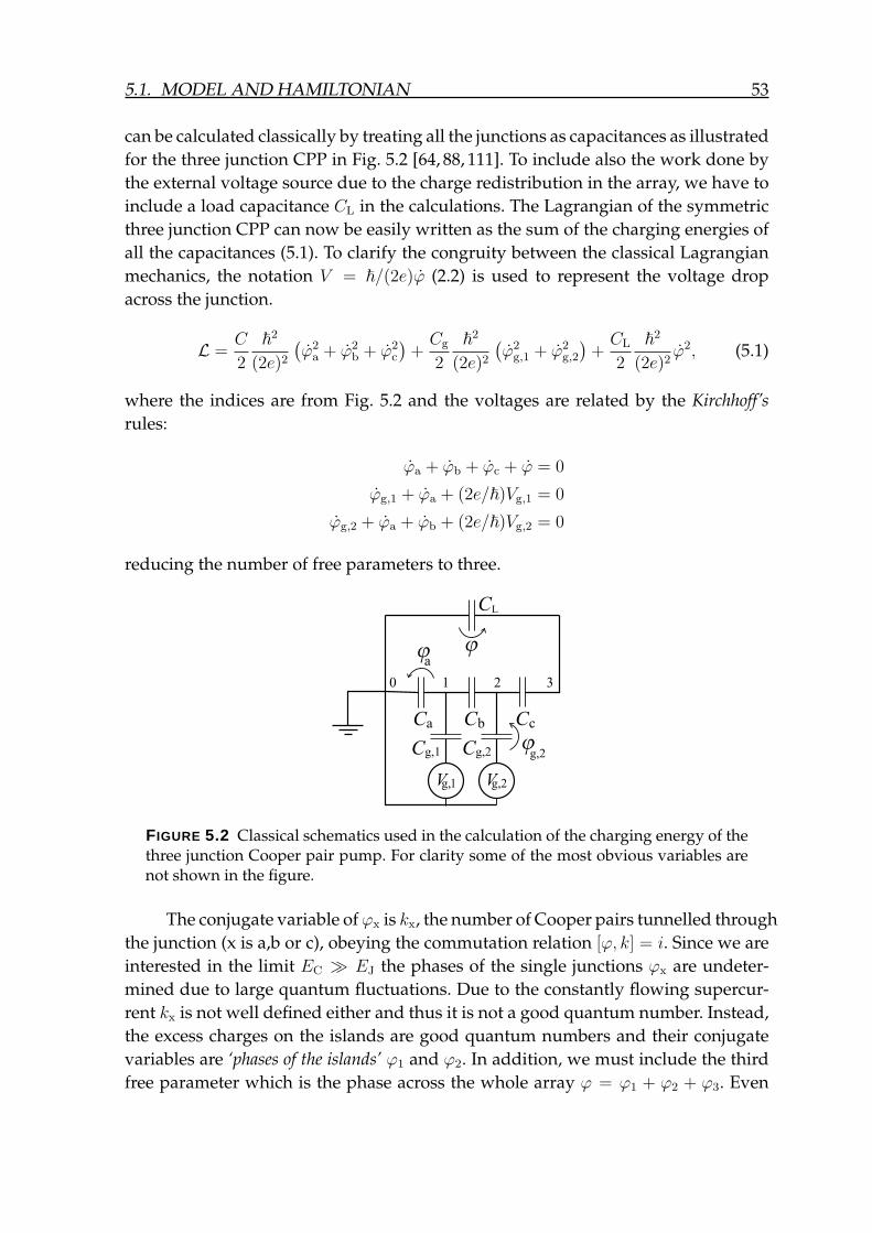
5.1. MODEL AND HAMILTONIAN 53
can be calculated classically by treating all the junctions as capacitances as illustratedfor the three junction CPP in Fig. 5.2 [64, 88, 111]. To include also the work done bythe external voltage source due to the charge redistribution in the array, we have toinclude a load capacitance CL in the calculations. The Lagrangian of the symmetricthree junction CPP can now be easily written as the sum of the charging energies ofall the capacitances (5.1). To clarify the congruity between the classical Lagrangianmechanics, the notation V = ~/(2e)ϕ (2.2) is used to represent the voltage dropacross the junction.
L =C
2
~2
(2e)2
(ϕ2
a + ϕ2b + ϕ2
c
)+Cg
2
~2
(2e)2
(ϕ2
g,1 + ϕ2g,2
)+CL
2
~2
(2e)2ϕ2, (5.1)
where the indices are from Fig. 5.2 and the voltages are related by the Kirchhoff’srules:
ϕa + ϕb + ϕc + ϕ = 0
ϕg,1 + ϕa + (2e/~)Vg,1 = 0
ϕg,2 + ϕa + ϕb + (2e/~)Vg,2 = 0
reducing the number of free parameters to three.
L
a
a
b c
0 1 2 3
FIGURE 5.2 Classical schematics used in the calculation of the charging energy of thethree junction Cooper pair pump. For clarity some of the most obvious variables arenot shown in the figure.
The conjugate variable ofϕx is kx, the number of Cooper pairs tunnelled throughthe junction (x is a,b or c), obeying the commutation relation [ϕ, k] = i. Since we areinterested in the limit EC EJ the phases of the single junctions ϕx are undeter-mined due to large quantum fluctuations. Due to the constantly flowing supercur-rent kx is not well defined either and thus it is not a good quantum number. Instead,the excess charges on the islands are good quantum numbers and their conjugatevariables are ‘phases of the islands’ ϕ1 and ϕ2. In addition, we must include the thirdfree parameter which is the phase across the whole array ϕ = ϕ1 + ϕ2 + ϕ3. Even
54 5. COOPER PAIR PUMP
though the phases of the invidual junctions are undetermined, the total phase ϕ isconstant of motion and thus fixed. We also determine the phases ϕ3 and ϕ0 (seeFig. 5.2) and the zero of the potential is chosen so that ϕ0 ≡ 0. The new variables caneasily be expressed using the old ones through Kirchhoff’s rules above:
ϕa = −ϕ1 ϕ = ϕ3
ϕb = ϕ1 − ϕ2 ϕg,1 = ϕ1 − (2e/~)Vg,1
ϕc = ϕ2 − ϕ ϕg,2 = ϕ2 − (2e/~)Vg,2.
Inserting these new variables into Eq. (5.1) we can write the Lagrangian in the matrixform:
L =1
2
~2
(2e)2ϕiCijϕj −
~2eJiϕi, (i, j = 1, 2, 3) (5.2)
where we have, for clarity, not written the sums explicitly out but the existence ofthe same index twice means summing over it. Symbol Cij is the capacitance matrixdefined as
Cij ≡ C
αg −1 0
−1 αg −1
0 −1 αL
and Ji ≡
Qg,1
Qg,2
0
. (5.3)
Here αg :=2 + Cg/C, αL :=1 + CL/C and Qg,i :=CgVg,i. Now the canonical momentacan be calculated using the definition
Pi =∂L∂ ~
2eϕi
=~2eCijϕi − Ji ⇒ ϕi =
2e
~C−1
ij (Pi + Ji), (5.4)
which yields
P1 = − ~2eCϕa +
~2eCϕb + CgVg,1 = Q1
P2 = − ~2eCϕb +
~2eCϕc + CgVg,2 = Q2 (5.5)
P3 = − ~2eCϕc +
~2eCLϕ = −Qc +QL := Q
The Hamiltonian describing the charging effects can now be calculated fromthe Lagrangian
HCh =~2eϕiPi − L
=~2eϕiPi −
1
2
~2
(2e)2ϕiCijϕj +
~2eJiϕi
= 12PiC
−1ij Pj + JiC
−1ij Pj, (5.6)
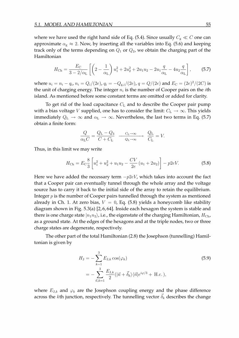
5.1. MODEL AND HAMILTONIAN 55
where we have used the right hand side of Eq. (5.4). Since usually Cg C one canapproximate αg ≈ 2. Now, by inserting all the variables into Eq. (5.6) and keepingtrack only of the terms depending on Q1 or Q2, we obtain the charging part of theHamiltonian
HCh =EC
3− 2/αL
[(2− 1
αL
)u2
1 + 2u22 + 2u1u2 − 2u1
q
αL
− 4u2q
αL
], (5.7)
where ui = ni − qi, ni = Qi/(2e), qi = −Qg,i/(2e), q = Q/(2e) and EC = (2e)2/(2C) isthe unit of charging energy. The integer ni is the number of Cooper pairs on the ithisland. As mentioned before some constant terms are omitted or added for clarity.
To get rid of the load capacitance CL and to describe the Cooper pair pumpwith a bias voltage V supplied, one has to consider the limit: CL → ∞. This yieldsimmediately QL → ∞ and αL → ∞. Nevertheless, the last two terms in Eq. (5.7)obtain a finite form:
Q
αLC=QL −Q3
C + CL
CL→∞−−−−−−−−→QL→∞
QL
CL
= V.
Thus, in this limit we may write
HCh = EC8
3
[u2
1 + u22 + u1u2 −
CV
2e(u1 + 2u2)
]− p2eV. (5.8)
Here we have added the necessary term −p2eV, which takes into account the factthat a Cooper pair can eventually tunnel through the whole array and the voltagesource has to carry it back to the initial side of the array to retain the equilibrium.Integer p is the number of Cooper pairs tunnelled through the system as mentionedalready in Ch. 1. At zero bias, V = 0, Eq. (5.8) yields a honeycomb like stabilitydiagram shown in Fig. 5.3(a) [2, 6, 64]. Inside each hexagon the system is stable andthere is one charge state |n1n2〉, i.e., the eigenstate of the charging Hamiltonian, HCh,as a ground state. At the edges of the hexagons and at the triple nodes, two or threecharge states are degenerate, respectively.
The other part of the total Hamiltonian (2.8) the Josephson (tunnelling) Hamil-tonian is given by
HJ = −3∑
k=1
EJ,k cos(ϕk) (5.9)
= −3∑
~n,k=1
EJ,k
2(|~n+ ~δk〉〈~n|eiϕ/3 + H.c. ),
where EJ,k and ϕk are the Josephson coupling energy and the phase differenceacross the kth junction, respectively. The tunnelling vector ~δk describes the change
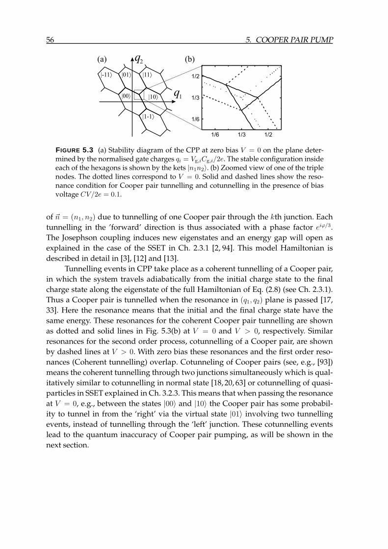
56 5. COOPER PAIR PUMP
|-11ñ
|1-1ñ
|11ñ
|10ñ
|01ñ
|00ñ q1
q2
1/6 1/3 1/2
1/6
1/3
1/2
(a) (b)
FIGURE 5.3 (a) Stability diagram of the CPP at zero bias V = 0 on the plane deter-mined by the normalised gate charges qi = Vg,iCg,i/2e. The stable configuration insideeach of the hexagons is shown by the kets |n1n2〉. (b) Zoomed view of one of the triplenodes. The dotted lines correspond to V = 0. Solid and dashed lines show the reso-nance condition for Cooper pair tunnelling and cotunnelling in the presence of biasvoltage CV/2e = 0.1.
of ~n = (n1, n2) due to tunnelling of one Cooper pair through the kth junction. Eachtunnelling in the ’forward’ direction is thus associated with a phase factor eiϕ/3.The Josephson coupling induces new eigenstates and an energy gap will open asexplained in the case of the SSET in Ch. 2.3.1 [2, 94]. This model Hamiltonian isdescribed in detail in [3], [12] and [13].
Tunnelling events in CPP take place as a coherent tunnelling of a Cooper pair,in which the system travels adiabatically from the initial charge state to the finalcharge state along the eigenstate of the full Hamiltonian of Eq. (2.8) (see Ch. 2.3.1).Thus a Cooper pair is tunnelled when the resonance in (q1, q2) plane is passed [17,33]. Here the resonance means that the initial and the final charge state have thesame energy. These resonances for the coherent Cooper pair tunnelling are shownas dotted and solid lines in Fig. 5.3(b) at V = 0 and V > 0, respectively. Similarresonances for the second order process, cotunnelling of a Cooper pair, are shownby dashed lines at V > 0. With zero bias these resonances and the first order reso-nances (Coherent tunnelling) overlap. Cotunneling of Cooper pairs (see, e.g., [93])means the coherent tunnelling through two junctions simultaneously which is qual-itatively similar to cotunnelling in normal state [18, 20, 63] or cotunnelling of quasi-particles in SSET explained in Ch. 3.2.3. This means that when passing the resonanceat V = 0, e.g., between the states |00〉 and |10〉 the Cooper pair has some probabil-ity to tunnel in from the ‘right’ via the virtual state |01〉 involving two tunnellingevents, instead of tunnelling through the ‘left’ junction. These cotunnelling eventslead to the quantum inaccuracy of Cooper pair pumping, as will be shown in thenext section.
5.2. PUMPED CURRENT 57
5.2 Pumped current
Pumping of Cooper pairs at V = 0 is achieved by adiabatically varying the gatevoltages along the path encircling one of the triple nodes. This is achieved, e.g., inthe case of three junction pump by the sinusoidal signals fed to the gates with 90
phase difference producing a circular path around the node as shown in Fig. 5.4(a),or by the pulses shown in Fig. 5.4(b) which produce a triangular path.
q
q
1
i
q2
1
1
0
0
t
(a) (b)
FIGURE 5.4 (a) The states with minimum charging energy of the uniform N = 3pump on the (q1, q2) plane. The small schematic figures illustrate the stable chargeconfiguration inside each hexagon. Two different pumping paths are shown by thickarrows. A circular path is produced by two sinusoidal gate voltages with 90 degreephase difference, and the triangular path by the gating sequence shown in (b).
The current pumped through an array ofN junctions when circling around thepumping path can be calculated using the adiabatic approximation of quantum me-chanics. The basis of instantaneous eigenstates |m(t)〉 with eigenenergies Em(t)of the full Hamiltonian (2.8) for a given ~q(t) = (q1, q2, . . .), is introduced for eachinstant of time t. If the state of the system is |m(t0)〉 at time t0 we can calculate thestate at t0 + δt using the time-dependent Schrödinger equation with the initial con-dition |ψ(t0)〉 = |m(t0)〉. Assuming slowly varying gate voltages we may solve theequation and obtain
|ψ(t0 + δt)〉 = e−iEm(t0)δt/~|m(t0)〉
+∑l 6=m
e−iEl(t0)δt/~ − e−iEm(t0)δt/~
i(El(t0)− Em(t0))/~〈l(t0)|~∇~qm(t0)〉 · (∂~q/∂t)|l(t0)〉
:= |m(t0 + δt)〉+ |δm(δt)〉, (5.10)
where the term |~∇~qm(t0)〉 · (∂~q/∂t) is the directional derivative of the state |m(t0)〉with respect to the change in gate charges ~q. The amount of charge passed throughthe kth junction, δQk, during a short time interval δt, can now be calculated by inte-
58 5. COOPER PAIR PUMP
grating the expectation value of the supercurrent operator
IS,k = −eEJ,k
~∑
~n
(−i|~n+ ~δk〉〈~n|eiϕ/N + H.c.
)(5.11)
over time δt, which yields
δQk =
∫ t0+δt
t0
〈ψ(t)|IS,k|ψ(t)〉dt
= δt〈IS,k〉|m(t0)〉 + 2Re
[∫ t0+δt
t0
〈m(t)|IS,k|δm(t− t0)〉dt]
(5.12)
= δt〈IS,k〉|m(t0)〉 − 2~∑l 6=m
Im
[〈m|IS,k|l〉〈l|δm〉
El − Em
]
where |δm〉 is the change in the instantaneous eigenstate induced by the change~q(t0) → ~q(t0 + δt). We have neglected the term quadratic in |δm〉 and oscillatoryterms by assuming small variation δ~q and that δt ~/(El − Em) holds for all l.
For a closed paths the total transferred charge must be equal for all the junc-tions due to the conservation of charge. Thus it is convenient to define also the (av-erage) supercurrent operator IS by
IS =1
N
N∑j=1
IS,j =(−2e)
~∂H
∂ϕ. (5.13)
The second equality follows from the ϕ-independence ofHCh and the relation∑
k ϕk
= ϕ. The common expectation value of IS and IS,k in a stationary state |m〉 is givenby (−2e/~)∂Em/∂ϕ where Em is the corresponding eigenenergy. Using IS we canexpress the total charge transferred through the array during one cycle along theclosed path
Q
−2e=
Qs
−2e+
QP
−2e=
1
~
∫ τ
0
∂Em(t)
∂φdt− 2~
−2e
∮ ∑l 6=m
Im
[〈m|IS|l〉〈l|dm〉El − Em
], (5.14)
where τ is the duration of the cycle.The obtained adiabatic evolution of the eigenstates splits the transferred charge
into two parts: the pumped charge QP and the charge QS carried by the constantlyflowing supercurrent IS. The latter one of these can be calculated as the ϕ-derivativeof the dynamical phase ηm = −
∫ t
0(Em(τ)/~)dτ in the state |m〉, QS/2e = −∂ηm/∂ϕ,
while the pumped charge is related to the ϕ-derivative of Berry’s phase [27] as willbe shown later.
For the three junction pump the pumped charge along the circular path shownin Fig. 5.4(a), can be calculated analytically in the lowest order in EJ/EC considering
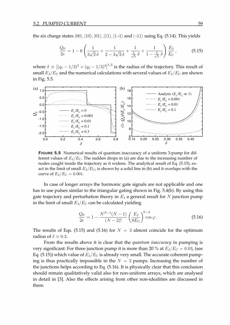
5.2. PUMPED CURRENT 59
the six charge states |00〉, |10〉, |01〉, |11〉, |1 -1〉 and | -11〉 using Eq. (5.14). This yields
QP
2e= 1− 6
(1
3√
2 δ+
1
2− 3√
2 δ+
13√5δ
+1
1− 3√5δ
)EJ
EC
, (5.15)
where δ ≡ [(q1 − 1/3)2 + (q2 − 1/3)2]1/2 is the radius of the trajectory. This result of
smallEJ/EC and the numerical calculations with several values ofEJ/EC are shownin Fig. 5.5.
(a) (b)
FIGURE 5.5 Numerical results of quantum inaccuracy of a uniform 3-pump for dif-ferent values of EJ/EC. The sudden drops in (a) are due to the increasing number ofnodes caught inside the trajectory as it widens. The analytical result of Eq. (5.15), ex-act in the limit of small EJ/EC, is shown by a solid line in (b) and it overlaps with thecurve of EJ/EC = 0.001.
In case of longer arrays the harmonic gate signals are not applicable and onehas to use pulses similar to the triangular gating shown in Fig. 5.4(b). By using thisgate trajectory and perturbation theory in EJ a general result for N junction pumpin the limit of small EJ/EC can be calculated yielding
QP
2e= 1− NN−1(N − 1)
(N − 2)!
(EJ
8EC
)N−2
cosϕ . (5.16)
The results of Eqs. (5.15) and (5.16) for N = 3 almost coincide for the optimumradius of δ ' 0.3.
From the results above it is clear that the quantum inaccuracy in pumping isvery significant: For three junction pump it is more than 20 % at EJ/EC = 0.03, (seeEq. (5.15)) which value ofEJ/EC is already very small. The accurate coherent pump-ing is thus practically impossible in the N = 3 pumps. Increasing the number ofthe junctions helps according to Eq. (5.16). It is physically clear that this conclusionshould remain qualitatively valid also for non-uniform arrays, which are analysedin detail in [3]. Also the effects arising from other non-idealities are discussed inthere.
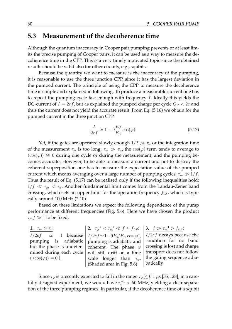
60 5. COOPER PAIR PUMP
5.3 Measurement of the decoherence time
Although the quantum inaccuracy in Cooper pair pumping prevents or at least lim-its the precise pumping of Cooper pairs, it can be used as a way to measure the de-coherence time in the CPP. This is a very timely motivated topic since the obtainedresults should be valid also for other circuits, e.g., squbits.
Because the quantity we want to measure is the inaccuracy of the pumping,it is reasonable to use the three junction CPP, since it has the largest deviation inthe pumped current. The principle of using the CPP to measure the decoherencetime is simple and explained in following. To produce a measurable current one hasto repeat the pumping cycle fast enough with frequency f . Ideally this yields theDC-current of I = 2ef , but as explained the pumped charge per cycle QP < 2e andthus the current does not yield the accurate result. From Eq. (5.16) we obtain for thepumped current in the three junction CPP
I
2ef' 1− 9
EJ
EC
cos(ϕ). (5.17)
Yet, if the gates are operated slowly enough 1/f τϕ or the integration timeof the measurement τm is too long, τm τϕ, the cos(ϕ) term tends to average to〈cos(ϕ)〉 ∼= 0 during one cycle or during the measurement, and the pumping be-comes accurate. However, to be able to measure a current and not to destroy thecoherent superposition one has to measure the expectation value of the pumpedcurrent which means averaging over a large number of pumping cycles, τm 1/f .Thus the result of Eq. (5.17) can be realised only if the following inequalities hold:1/f τm < τϕ. Another fundamental limit comes from the Landau-Zener bandcrossing, which sets an upper limit for the operation frequency fLZ, which is typi-cally around 100 MHz (2.10).
Based on these limitations we expect the following dependence of the pumpperformance at different frequencies (Fig. 5.6). Here we have chosen the productτmf 1 to be fixed.
1. τm > τϕ:
I/2ef ' 1 becausepumping is adiabaticbut the phase is undeter-mined during each cycle( 〈cos(ϕ)〉 = 0 ).
2. τ−1ϕ < τ−1
m f ≤ fLZ :
I/2ef'1−9EJ/EC cos(ϕ),pumping is adiabatic andcoherent. The phase ϕwill still drift on a timescale longer than τϕ.(Shaded area in Fig. 5.6)
3. f τ−1m > fLZ :
I/2ef decays because thecondition for no bandcrossing is lost and chargetransport does not followthe gating sequence adia-batically.
Since τϕ is presently expected to fall in the range τϕ & 0.1 µs [35,128], in a care-fully designed experiment, we would have τ−1
ϕ < 50 MHz, yielding a clear separa-tion of the three pumping regimes. In particular, if the decoherence time of a squbit
5.4. BERRY’S PHASE AND ITS RELATION TO PUMPED CURRENT 61
FIGURE 5.6 A schematic presentation of the expected behaviour of the pumped cur-rent in the three junction Cooper pair pump as a function of inverse of the measuringtime 1/τm. The product of the pumping frequency f and the measuring time is sup-posed to be fixed τmf 1. The shaded area covers the different values of the phasedifference ϕ across the array.
and thus also τϕ turns out to be of the order of 1 µs [4], which would allow quantumcomputation by Josephson qubits in this respect, τ−1
ϕ would give an experimentallyconvenient crossover frequency in the MHz range.
5.4 Berry’s phase and its relation to pumped current
In 1984 Berry pointed out that if the system undergoes an adiabatic change, i.e., thesystem parameters ~p = pii in its Hamiltonian H(~pi) are adiabatically altered, theeigenstate |ψ〉 attains a geometrical phase factor exp[iγ(Γ)], in addition to the regulardynamic phase [27]. This phase, γ, is called Berry’s phase and it depends on thepath Γ in the parameter space along which the system has traversed. Particularly, ifthe parameters are returned to their original values the eigenstate will return to itsoriginal form apart from the phase factor. This phase cannot be directly measuredexcept via interference between another state, e.g., a similar state which has beenstationary from the beginning of the process. The dynamical phase obtained alongthe adiabatic change depends on the path and the duration of the process whereasBerry’s phase depends only on the path chosen. It has also been proposed that asqubit could be constructed using Berry’s phase instead of charge or flux [52].
To derive a general formula for the Berry’s phase attained during traversingthe path Γ, the basis consisting of the eigenvectors |m(~p )〉 with energies Em(~p ) isintroduced so that H(~p )|m(~p )〉 = Em(~p )|m(~p )〉. Now we make an ansatz for theeigenstate at the time t
|ψ(t)〉 = eiγm(t)− i
~
t∫0
Em(~p (t′))dt′
|m (~p (t))〉 (5.18)
62 5. COOPER PAIR PUMP
and insert that into the time dependent Schrödinger equation, which immediatelyyields
dγm(t)
dt= i
⟨m(~p (t))
∣∣∣∣ ddt∣∣∣∣m(~p (t))
⟩, (5.19)
whereby
γm(t) = i
∫ t
0
⟨m(~p (t′))
∣∣∣∣ ddt′∣∣∣∣m(~p (t′))
⟩dt′
= i
∫ ~p (t)
~p (0)
⟨m(~p )
∣∣∣~∇~p
∣∣∣m(~p )⟩d~p
=: i
∫ ~p (t)
~p (0)
〈m|dm〉, (5.20)
where |dm〉 is given by Eq. (5.10). This equation is naturally a general form of Berry’sphase in any system with eigenvectors |m〉. The notation we use is similar to the oneused in derivation of the pumped current to clarify the relation between them. Inthe case of the CPP pii=1,...,N = qi, ϕi=1,...,N−1. For a closed path Γ : t 7→ ~p (t) witht ∈ [0, τ ] and ~p (0) = ~p (τ), the last integral and thus Berry’s phase seem to vanish.However, the integrand is not necessarily a total derivative, especially if the pathencircles a node in the parameter space, e.g., the triple node in the stability diagramof the CPP, which yields
γm(Γ) = i
∮Γ
〈m|dm〉 6= 0. (5.21)
Using Stokes theorem and the methods of differential geometry it can be shownthat Berry’s phase for a closed path Γ can be calculated by integrating Berry’s curva-ture over a two-surface [5, 100, 119]
γm(Γ) = i
N∑k=1
N∑l=1
∫∫SΓ
∂〈m|∂qk
∂|m〉∂ql
dqk ∧ dql, (5.22)
where the boundary of SΓ is the path Γ. 1 To show how the pumped current in theCPP is related to Berry’s phase we construct an extended path for which Berry’sphase is proportional to the charge pumped along the path Γ. To do that a classof closed paths Γφ has to be defined as Γφ : t 7→ ~p (t) = (~q (t), ϕ(t) + φ), wheret ∈ [0, τ ], so that Γ0 = Γ, and also another class of paths φ~p is defined accordingto φ~p : t 7→ (~q, ϕ + tφ), where t ∈ [0, 1]. The inverse of a path φ−1
~p is the same pathtraversed in the opposite direction. The extended path
Γφext := Γ0 φ~p (0) Γ−1
φ φ−1~p (0) (5.23)
1It suffices to state that dx ∧ dy = −dy ∧ dx is a generalisation of two-dimensional integral ontocurved manifolds and that for a flat surface it reduces to the conventional dxdy.
5.4. BERRY’S PHASE AND ITS RELATION TO PUMPED CURRENT 63
is also closed and spans a two-dimensional integration surface whose width in ϕ-direction is φ as shown in Fig. 5.7(b). By traversing the boundary the contributionsfrom φ~p (0) and φ−1
~p (0) naturally cancel, and we find
γ(Γφext) = γ(Γ)− γ(Γφ). (5.24)
The pumped charge along the path Γ is given by Eq. (5.14) and can also bewritten as [13]
QP
−2e= 2
∮Γ
Re[〈m|M |dm〉
],
= iN∑
k=1
∮Γ
[∂〈m|∂ϕ
∂|m〉∂qk
− ∂〈m|∂qk
∂|m〉∂ϕ
]dqk, (5.25)
where M = −i∂/∂ϕ is the operator for the average number of tunnelled Cooperpairs. This closely reminds the formulas (5.22) and (5.21) on Berry’s phase.
Considering the extended path Γφext in the limit φ → 0, i.e., in the case of a
strip of infinitesimal width dϕ between Γdϕ and Γ0, one can express Berry’s phaseattained, γm(Γdϕ
ext), using Eq. (5.22). Now in Eq. (5.22) either dqk = dϕ or dql = dϕ
as the full length of integration. Thus dϕ can be factored out from the expressionyielding the result of Eq. (5.25) multiplied by −dϕ. The same result can be writtenusing Eq. (5.24) and by taking the limit limφ→0[γ(Γ)− γ(Γφ)]/φ, one obtains [5]
QP/2e = ∂γm/∂ϕ (5.26)
similarly toQS/2e = ∂ηm/∂ϕ . (5.27)
Let us consider a closed path Γ corresponding to a fixed value of ϕ0 as inRef. [2]. Under ideal operation of gate and bias voltages one can change ϕ slightlybetween each cycle to evenly cover a strip in the parameter space pii=1,...,N =
qi, ϕi=1,...,N−1 bounded by the planes ϕ = ϕ0 and ϕ = ϕ0+φ as shown in Fig. 5.7(d).On the other hand by integrating Eq. (5.26) with respect to ϕ over the set Γφ, theaverage pumped charge QP,ave can be defined as
QP,ave =1
φ
∫ φ
0
QP(Γϕ)dϕ =γ(Γ0)− γ(Γφ)
φ. (5.28)
Combining these two results one obtains an important result for an ideal CPP: themeasured pumped charge per cycle (i.e. QP,ave) yields direct information about dif-ferences of Berry’s phases.
In a real experiment neither the phase difference, ϕ, nor the gate voltages areideally controlled. Yet, it has to be assumed that the gate voltages are operated ac-
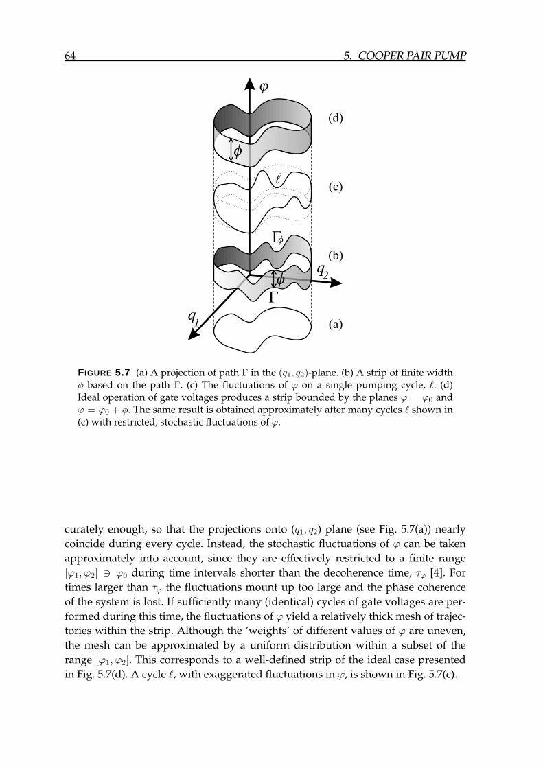
64 5. COOPER PAIR PUMP
f
q1
q2
G
G
j
l
(a)
(b)
(c)
(d)
f
f
FIGURE 5.7 (a) A projection of path Γ in the (q1, q2)-plane. (b) A strip of finite widthφ based on the path Γ. (c) The fluctuations of ϕ on a single pumping cycle, `. (d)Ideal operation of gate voltages produces a strip bounded by the planes ϕ = ϕ0 andϕ = ϕ0 + φ. The same result is obtained approximately after many cycles ` shown in(c) with restricted, stochastic fluctuations of ϕ.
curately enough, so that the projections onto (q1, q2) plane (see Fig. 5.7(a)) nearlycoincide during every cycle. Instead, the stochastic fluctuations of ϕ can be takenapproximately into account, since they are effectively restricted to a finite range[ϕ1, ϕ2] 3 ϕ0 during time intervals shorter than the decoherence time, τϕ [4]. Fortimes larger than τϕ the fluctuations mount up too large and the phase coherenceof the system is lost. If sufficiently many (identical) cycles of gate voltages are per-formed during this time, the fluctuations of ϕ yield a relatively thick mesh of trajec-tories within the strip. Although the ’weights’ of different values of ϕ are uneven,the mesh can be approximated by a uniform distribution within a subset of therange [ϕ1, ϕ2]. This corresponds to a well-defined strip of the ideal case presentedin Fig. 5.7(d). A cycle `, with exaggerated fluctuations in ϕ, is shown in Fig. 5.7(c).
5.5. TURNSTILE KIND OF BEHAVIOUR 65
5.5 Turnstile kind of behaviour
As everything in the last section was derived at zero bias, in this section the effectsdue to non-zero bias voltage applied to the system are considered. Since the res-onances of coherent tunnelling and cotunnelling separate at non-zero bias voltageV as explained in Ch. 5.1, each degeneracy node in stability diagram is split intoa triangle determined by the first order tunnelling resonances, as shown by solidlines in Fig. 5.3(b) [29, 64]. Inside the triangles the state of the CPP depends on thepath along which the system has reached the point, thus opening the possibility forhysteretic behavior leading to a turnstile kind of operation.
The operation of the three junction pump as a turnstile is achieved by travers-ing back and forth along a path in (q1, q2) plane with the constraint q1 = q2 + k2e,exiting the triangle at both extremes as pictured in Fig. 5.8(a). Here k is any integernumber. The simplest way to describe the behaviour is to assume that at every res-onance, the system is driven to the state with lower energy. This simple reasoningalone is enough to explain the turnstile kind of behaviour: within every traversal ofthe path one Cooper pair is transferred through the array in the direction of the biasvoltage.
To explain this principle of operation in more detail one has to take into ac-count the dissipation in the system. The adiabatic passing through the degeneracyline of charging energy HCh will induce the coherent tunnelling of a Cooper pair asexplained in Ch. 2.3.1 and the limit for the adiabaticity is determined by Eq. (2.10)with q =
√q21 + q2
2 . In the absence of dissipation the probability for band crossingis equal in both directions, i.e., to excite or relax the system, but with dissipationthe symmetry breaks. The probability to excite the system retains the same ampli-tude, PLZ, but the probability for relaxation PRel = 1 − PLZ + P 2
LZ is significantlyincreased, and reaches almost unity in the case of strong coupling to a dissipativeelement [10, 94]. Thus, to really obtain the hysteretic behavior one needs dissipa-tion in the system. This can be provided, e.g., by the electromagnetic environmentor quasiparticles, which both can absorb any amount of energy dissipated from thesystem.
The energy diagram of the CPP along the path, [t 7→ (q1, q2) : q1(t) = q2(t)+k2e]
crossing the triangle as shown in Fig. 5.8(a) is plotted in Fig. 5.8(b). To be able toproperly explain the behaviour we have to include in our notation the number ofCooper pairs tunnelled through the array: instead of |n1n2〉 we write |n1n2, p〉. Ifthe system is initially in the state |00, 0〉 and we start to increase both gates, i.e.,to move from left to right along the x-axis in Fig. 5.8(b), we come to the point ofresonance for tunnelling through two junctions simultaneously, i.e., cotunnelling, tothe state |01, 0〉. In the case of cotunnelling the total coupling for one Cooper pairto tunnel through two junctions, Eco
J , depends on the EJ of the junctions and theenergy of the intermediate virtual state. This resonance condition is indicated by adashed line in Fig. 5.8(a) and the cotunnelling is now assumed to take place. When
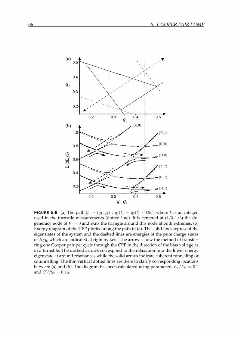
66 5. COOPER PAIR PUMP
q1
q1
q2
q2
0.2 0.3 0.4 0.5
0.2
0.4
0.6
0.8
1.0
E(8
EC/3
)
|00,0ñ
|00,1ñ
|10,0ñ
|01,0ñ
|00,2ñ
|10,1ñ
|01,1ñ
(a)
(b)
,
0.2
0.2
0.3
0.3
0.4
0.4
0.5
0.5
FIGURE 5.8 (a) The path [t 7→ (q1, q2) : q1(t) = q2(t) + k2e], where k is an integer,used in the turnstile measurements (dotted line). It is centered at (1/3, 1/3) the de-generacy node of V = 0 and exits the triangle around this node at both extremes. (b)Energy diagram of the CPP plotted along the path in (a). The solid lines represent theeigenstates of the system and the dashed lines are energies of the pure charge statesof HCh, which are indicated at right by kets. The arrows show the method of transfer-ring one Cooper pair per cycle through the CPP in the direction of the bias voltage asin a turnstile. The dashed arrows correspond to the relaxation into the lower energyeigenstate at around resonances while the solid arrays indicate coherent tunnelling orcotunnelling. The thin vertical dotted lines are there to clarify corresponding locationsbetween (a) and (b). The diagram has been calculated using parameters EJ/EC = 0.2and CV/2e = 0.16.
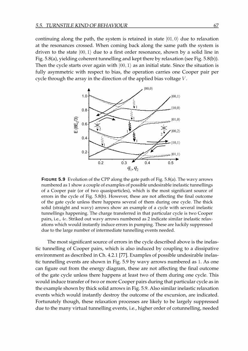
5.5. TURNSTILE KIND OF BEHAVIOUR 67
continuing along the path, the system is retained in state |01, 0〉 due to relaxationat the resonances crossed. When coming back along the same path the system isdriven to the state |00, 1〉 due to a first order resonance, shown by a solid line inFig. 5.8(a), yielding coherent tunnelling and kept there by relaxation (see Fig. 5.8(b)).Then the cycle starts over again with |00, 1〉 as an initial state. Since the situation isfully asymmetric with respect to bias, the operation carries one Cooper pair percycle through the array in the direction of the applied bias voltage V .
q1
q2
0.2 0.3 0.4 0.5
0.2
0.4
0.6
0.8
1.0
E(8
EC/3
)
|00,0ñ
|00,1ñ
|10,0ñ
|01,0ñ
|00,2ñ
|10,1ñ
|01,1ñ
,
1
1
1
1
2
2
1
FIGURE 5.9 Evolution of the CPP along the gate path of Fig. 5.8(a). The wavy arrowsnumbered as 1 show a couple of examples of possible undesirable inelastic tunnellingsof a Cooper pair (or of two quasiparticles), which is the most significant source oferrors in the cycle of Fig. 5.8(b). However, these are not affecting the final outcomeof the gate cycle unless there happens several of them during one cycle. The thicksolid (straight and wavy) arrows show an example of a cycle with several inelastictunnellings happening. The charge transferred in that particular cycle is two Cooperpairs, i.e., 4e. Striked out wavy arrows numbered as 2 indicate similar inelastic relax-ations which would instantly induce errors in pumping. These are luckily suppresseddue to the large number of intermediate tunnelling events needed.
The most significant source of errors in the cycle described above is the inelas-tic tunnelling of Cooper pairs, which is also induced by coupling to a dissipativeenvironment as described in Ch. 4.2.1 [77]. Examples of possible undesirable inelas-tic tunnelling events are shown in Fig. 5.9 by wavy arrows numbered as 1. As onecan figure out from the energy diagram, these are not affecting the final outcomeof the gate cycle unless there happens at least two of them during one cycle. Thiswould induce transfer of two or more Cooper pairs during that particular cycle as inthe example shown by thick solid arrows in Fig. 5.9. Also similar inelastic relaxationevents which would instantly destroy the outcome of the excursion, are indicated.Fortunately though, these relaxation processes are likely to be largely suppresseddue to the many virtual tunnelling events, i.e., higher order of cotunnelling, needed
68 5. COOPER PAIR PUMP
in them. These processes are shown by thin wavy arrows striked out and numberedas 2. Thus, the system is fairly rigidly ’locked’ to transfer only one Cooper pair percycle.
6 Experiments with the Cooper pairpump
In this chapter experiments on a Cooper pair pump are presented. As all the mea-surements are explained in detail in Ref. [7], only the major results are reviewedhere. The Cooper pair pump was measured to test the preceding theoretical modelsof the pumping and turnstile kind of behaviour. The measured sample was fabri-cated along the recipe presented in Ch. 2.2.1 and the experimental setup used wasexplained already in Ch. 2.2.2. All the measurements were carried out at the basetemperature ∼20 mK. Since room temperature equipment was used in the biasingcircuit, the decoherence rate obtained was supposed to be extremely fast preventingany possibility to observe coherence induced inaccuracy in the pumping. Neverthe-less, even the incoherent pumping resulting in the current I = 2ef has not beenreliably observed in a CPP [64, 135].
6.1 Sample characterisation
In Fig. 6.1 I-V characteristics of the sample, taken with different combinations ofgate voltages Vg,1 and Vg,2 are presented. It shows sharp jumps at the beginning ofthe quasiparticle tunnelling branches at bias voltage V '±6∆Al/e≈±1.2 mV. Alsoall four major peaks in subgap regime corresponding to different possibilities ofJQP -cycles are clearly visible [16, 33, 61, 101]. In the large scale figure (a) the currentaround zero bias is not visible but it is seen in the blow up (b). The supercurrent,i.e., the feature around zero bias, is not present at V = 0 but it is peaked around it,having the maximum at |V |EC/e (see Fig. 6.1(b)). The shape of the supercurrentfeature indicates electromagnetic environment Z(ω), with very low impedance of0<Re[Z(ω)]RQ (see Ch. 4.2.1). This agrees well with the impedance of the biasinglines, which is of the order of the vacuum impedance
√µ0/ε0 ' 377 Ω. Resonance
peaks symmetrically around zero bias at V ≈±80 µV, are also visible in this figure,and they are due to the effect of the bias voltage on the stability diagram [7]. Thegate modulation is most pronounced at the gap edge as well as in the region of JQP-peaks and the supercurrent. The obtained sample parameters are presented in Table6.1.
69
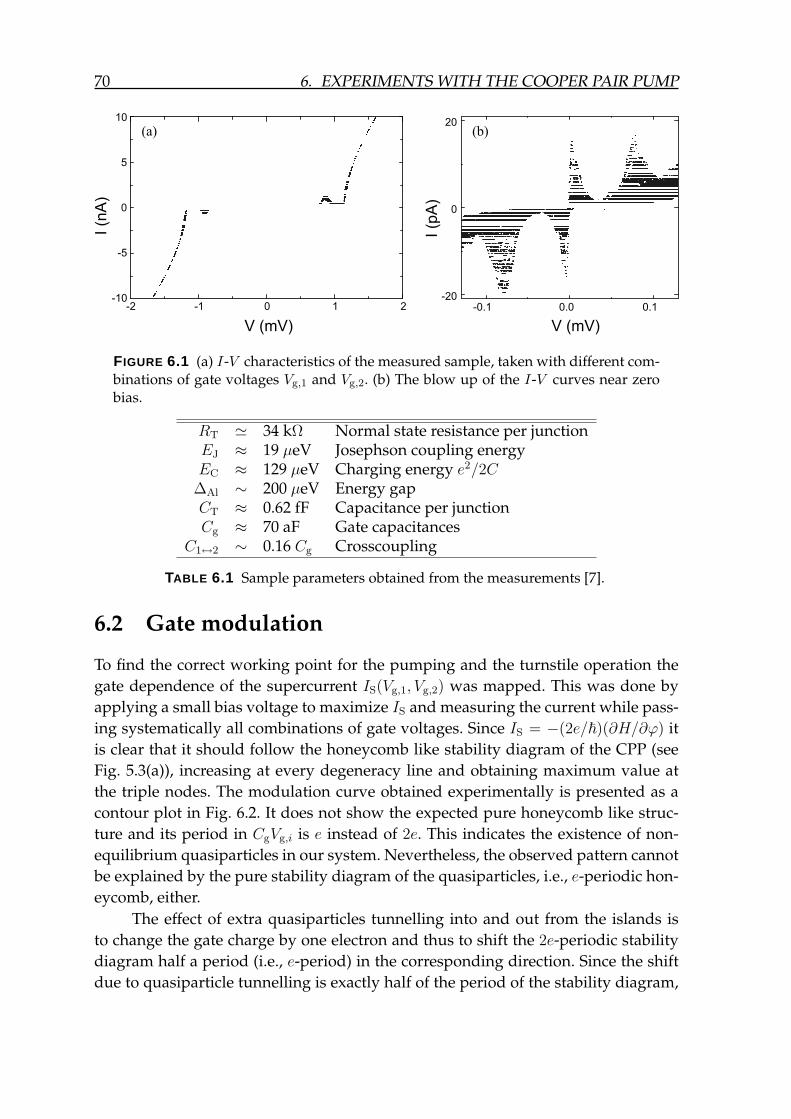
70 6. EXPERIMENTS WITH THE COOPER PAIR PUMP
-2 -1 0 1 2-10
-5
0
5
10
I (n
A)
V (mV) V (mV)
-0.1 0.0 0.1-20
0
20
I (p
A)
(a) (b)
FIGURE 6.1 (a) I-V characteristics of the measured sample, taken with different com-binations of gate voltages Vg,1 and Vg,2. (b) The blow up of the I-V curves near zerobias.
RT ' 34 kΩ Normal state resistance per junctionEJ ≈ 19 µeV Josephson coupling energyEC ≈ 129 µeV Charging energy e2/2C∆Al ∼ 200 µeV Energy gapCT ≈ 0.62 fF Capacitance per junctionCg ≈ 70 aF Gate capacitances
C1↔2 ∼ 0.16 Cg Crosscoupling
TABLE 6.1 Sample parameters obtained from the measurements [7].
6.2 Gate modulation
To find the correct working point for the pumping and the turnstile operation thegate dependence of the supercurrent IS(Vg,1, Vg,2) was mapped. This was done byapplying a small bias voltage to maximize IS and measuring the current while pass-ing systematically all combinations of gate voltages. Since IS = −(2e/~)(∂H/∂ϕ) itis clear that it should follow the honeycomb like stability diagram of the CPP (seeFig. 5.3(a)), increasing at every degeneracy line and obtaining maximum value atthe triple nodes. The modulation curve obtained experimentally is presented as acontour plot in Fig. 6.2. It does not show the expected pure honeycomb like struc-ture and its period in CgVg,i is e instead of 2e. This indicates the existence of non-equilibrium quasiparticles in our system. Nevertheless, the observed pattern cannotbe explained by the pure stability diagram of the quasiparticles, i.e., e-periodic hon-eycomb, either.
The effect of extra quasiparticles tunnelling into and out from the islands isto change the gate charge by one electron and thus to shift the 2e-periodic stabilitydiagram half a period (i.e., e-period) in the corresponding direction. Since the shiftdue to quasiparticle tunnelling is exactly half of the period of the stability diagram,
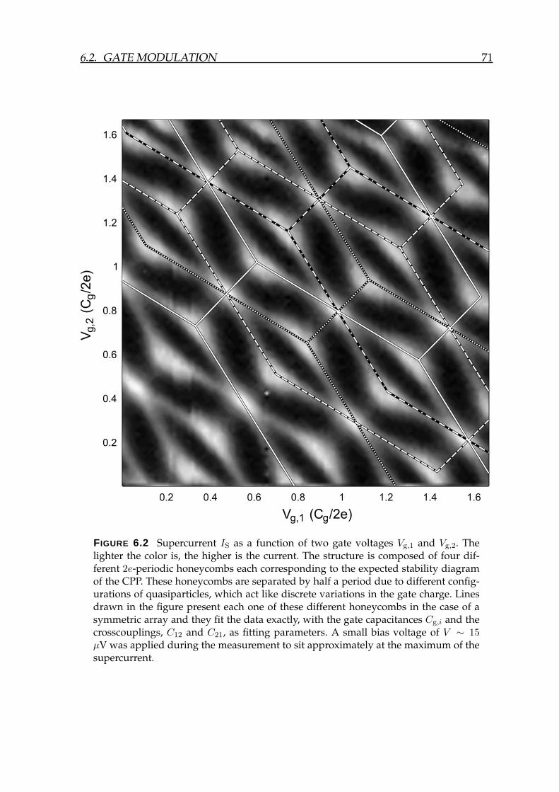
6.2. GATE MODULATION 71
V (C /2e)g,1 g
V(C
/2e
)g
,2g
FIGURE 6.2 Supercurrent IS as a function of two gate voltages Vg,1 and Vg,2. Thelighter the color is, the higher is the current. The structure is composed of four dif-ferent 2e-periodic honeycombs each corresponding to the expected stability diagramof the CPP. These honeycombs are separated by half a period due to different config-urations of quasiparticles, which act like discrete variations in the gate charge. Linesdrawn in the figure present each one of these different honeycombs in the case of asymmetric array and they fit the data exactly, with the gate capacitances Cg,i and thecrosscouplings, C12 and C21, as fitting parameters. A small bias voltage of V ∼ 15µV was applied during the measurement to sit approximately at the maximum of thesupercurrent.
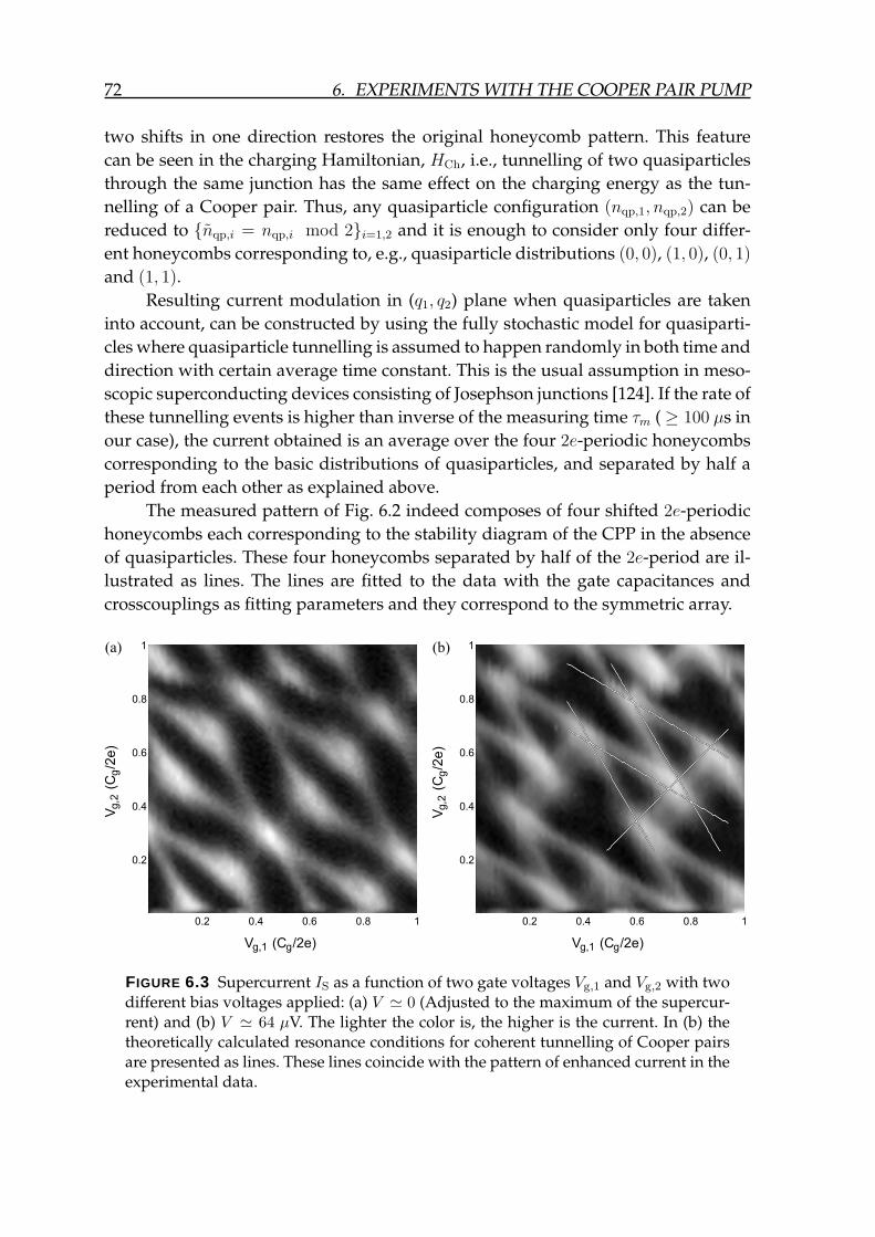
72 6. EXPERIMENTS WITH THE COOPER PAIR PUMP
two shifts in one direction restores the original honeycomb pattern. This featurecan be seen in the charging Hamiltonian, HCh, i.e., tunnelling of two quasiparticlesthrough the same junction has the same effect on the charging energy as the tun-nelling of a Cooper pair. Thus, any quasiparticle configuration (nqp,1, nqp,2) can bereduced to nqp,i = nqp,i mod 2i=1,2 and it is enough to consider only four differ-ent honeycombs corresponding to, e.g., quasiparticle distributions (0, 0), (1, 0), (0, 1)
and (1, 1).Resulting current modulation in (q1, q2) plane when quasiparticles are taken
into account, can be constructed by using the fully stochastic model for quasiparti-cles where quasiparticle tunnelling is assumed to happen randomly in both time anddirection with certain average time constant. This is the usual assumption in meso-scopic superconducting devices consisting of Josephson junctions [124]. If the rate ofthese tunnelling events is higher than inverse of the measuring time τm (≥ 100 µs inour case), the current obtained is an average over the four 2e-periodic honeycombscorresponding to the basic distributions of quasiparticles, and separated by half aperiod from each other as explained above.
The measured pattern of Fig. 6.2 indeed composes of four shifted 2e-periodichoneycombs each corresponding to the stability diagram of the CPP in the absenceof quasiparticles. These four honeycombs separated by half of the 2e-period are il-lustrated as lines. The lines are fitted to the data with the gate capacitances andcrosscouplings as fitting parameters and they correspond to the symmetric array.
V(C
/2e
)g,2
g
(a)
V(C
/2e
)g,2
g
V (C /2e)g,1 gV (C /2e)g,1 g
Vg1
(b)
FIGURE 6.3 Supercurrent IS as a function of two gate voltages Vg,1 and Vg,2 with twodifferent bias voltages applied: (a) V ' 0 (Adjusted to the maximum of the supercur-rent) and (b) V ' 64 µV. The lighter the color is, the higher is the current. In (b) thetheoretically calculated resonance conditions for coherent tunnelling of Cooper pairsare presented as lines. These lines coincide with the pattern of enhanced current in theexperimental data.
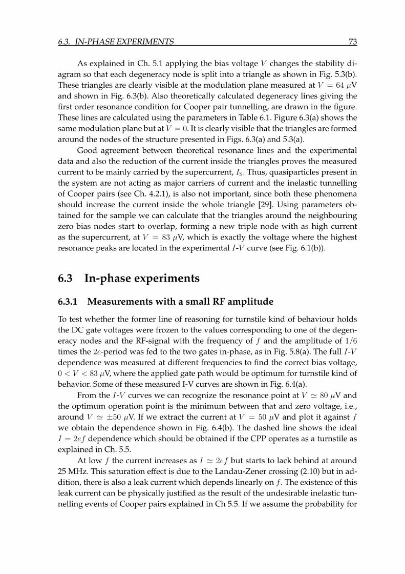
6.3. IN-PHASE EXPERIMENTS 73
As explained in Ch. 5.1 applying the bias voltage V changes the stability di-agram so that each degeneracy node is split into a triangle as shown in Fig. 5.3(b).These triangles are clearly visible at the modulation plane measured at V = 64 µVand shown in Fig. 6.3(b). Also theoretically calculated degeneracy lines giving thefirst order resonance condition for Cooper pair tunnelling, are drawn in the figure.These lines are calculated using the parameters in Table 6.1. Figure 6.3(a) shows thesame modulation plane but at V = 0. It is clearly visible that the triangles are formedaround the nodes of the structure presented in Figs. 6.3(a) and 5.3(a).
Good agreement between theoretical resonance lines and the experimentaldata and also the reduction of the current inside the triangles proves the measuredcurrent to be mainly carried by the supercurrent, IS. Thus, quasiparticles present inthe system are not acting as major carriers of current and the inelastic tunnellingof Cooper pairs (see Ch. 4.2.1), is also not important, since both these phenomenashould increase the current inside the whole triangle [29]. Using parameters ob-tained for the sample we can calculate that the triangles around the neighbouringzero bias nodes start to overlap, forming a new triple node with as high currentas the supercurrent, at V = 83 µV, which is exactly the voltage where the highestresonance peaks are located in the experimental I-V curve (see Fig. 6.1(b)).
6.3 In-phase experiments
6.3.1 Measurements with a small RF amplitude
To test whether the former line of reasoning for turnstile kind of behaviour holdsthe DC gate voltages were frozen to the values corresponding to one of the degen-eracy nodes and the RF-signal with the frequency of f and the amplitude of 1/6
times the 2e-period was fed to the two gates in-phase, as in Fig. 5.8(a). The full I-Vdependence was measured at different frequencies to find the correct bias voltage,0 < V < 83 µV, where the applied gate path would be optimum for turnstile kind ofbehavior. Some of these measured I-V curves are shown in Fig. 6.4(a).
From the I-V curves we can recognize the resonance point at V ' 80 µV andthe optimum operation point is the minimum between that and zero voltage, i.e.,around V ' ±50 µV. If we extract the current at V = 50 µV and plot it against fwe obtain the dependence shown in Fig. 6.4(b). The dashed line shows the idealI = 2ef dependence which should be obtained if the CPP operates as a turnstile asexplained in Ch. 5.5.
At low f the current increases as I ' 2ef but starts to lack behind at around25 MHz. This saturation effect is due to the Landau-Zener crossing (2.10) but in ad-dition, there is also a leak current which depends linearly on f . The existence of thisleak current can be physically justified as the result of the undesirable inelastic tun-nelling events of Cooper pairs explained in Ch 5.5. If we assume the probability for
74 6. EXPERIMENTS WITH THE COOPER PAIR PUMP
(a) (b)
FIGURE 6.4 (a) The I-V curves measured with DC gate voltages tuned to one of thedegeneracy nodes and in-phase sinusoidal RF signals added to the two gates corre-sponding to the path shown in Fig. 5.8(a). Amplitude used was 1/6 × 2e-period andfrequencies corresponding to I-V curves from lowest to highest absolute current levelare 0.5, 6, 12, 18, 26, 40 and 60 MHz. (b) Current ∆I ≡ I − I0 extracted from the I-Vcurves in (a) at V = 50 µV as a function of the frequency of the RF signals appliedin-phase to the two gates. The solid line is the fit by Eq. (6.1) and values for the fitparameters are shown in the first line of Table 6.2 with the exception of I0. The insetshows the same current with the leak current subtracted and the dashed line showsthe ideal 2ef dependence predicted by the theory.
inelastic tunnelling PIT to be independent of frequency, we obtain an approximateexpression for the leak current, Ileak = [2eP 2
IT +O(P 4IT)]f , which depends linearly on
f . The function which was used to fit the data and is shown in Fig. 6.4(b), is of theform
I = 2efQP
(1− e−fLZ/f
)+ 2efQL + I0, (6.1)
where the fit parameters are fLZ, I0 the offset in current, QP and QL, which are thecharges transferred and leaked during one cycle in units of 2e, respectively. Theanalysis of the data was done both at negative and positive bias voltages. We alsorepeated the measurement in another node with slightly larger amplitude (1/4× 2e-period) of RF signal and these results are also shown in Table 6.2.
As seen from Table 6.2, the obtained frequency dependence agrees with thetheoretical prediction of 2ef at low frequencies, i.e., QP ≈ 1. However, the Landau-Zener frequency obtained, fLZ ∼ 30 MHz, is lower than that estimated ∼ 65 MHzfor cotunnelling. This discrepancy can be explained with the small inhomogeneityof the sample [6]. For the leaked charge we obtained QL ∼ 0.17, which correspondsto a 17 % probability for an extra Cooper pair to leak via inelastic tunnelling eventsshown in Fig. 5.9, during one cycle.
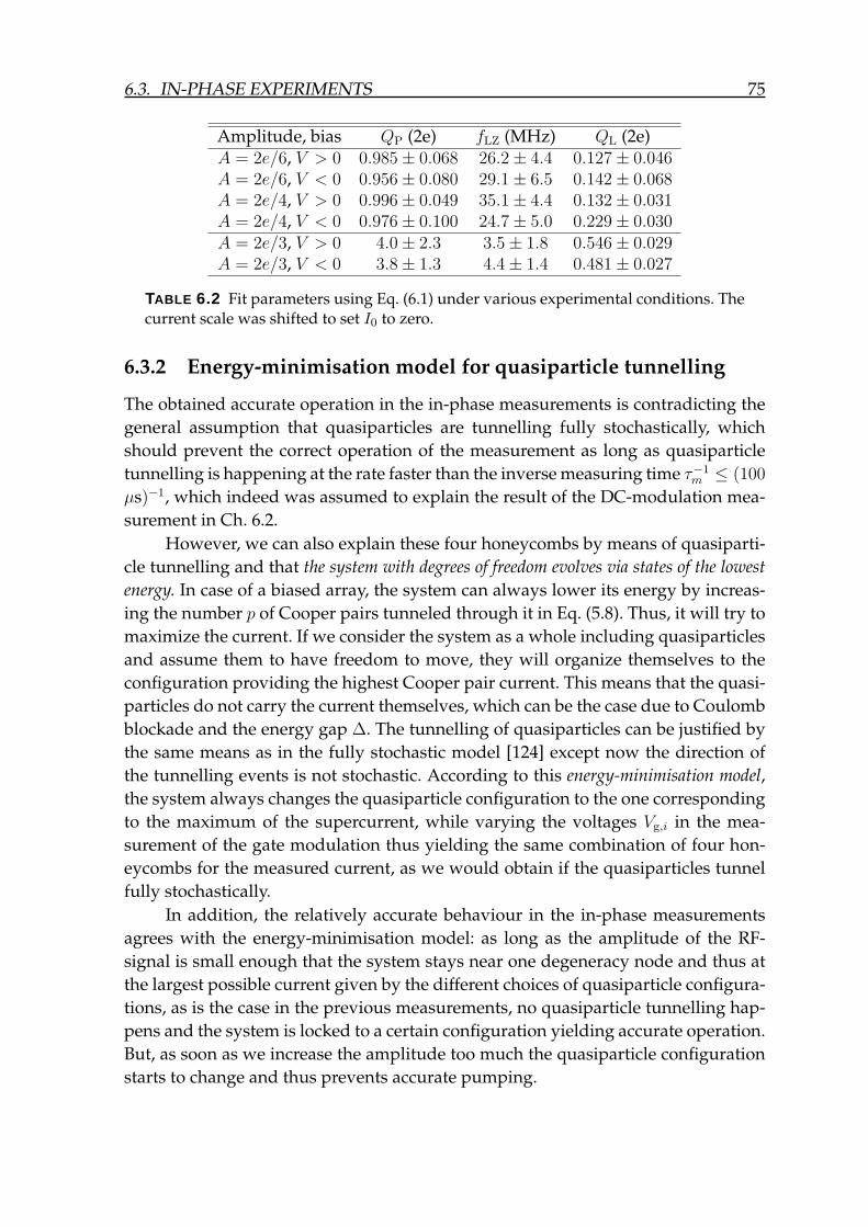
6.3. IN-PHASE EXPERIMENTS 75
Amplitude, bias QP (2e) fLZ (MHz) QL (2e)A = 2e/6, V > 0 0.985± 0.068 26.2± 4.4 0.127± 0.046A = 2e/6, V < 0 0.956± 0.080 29.1± 6.5 0.142± 0.068A = 2e/4, V > 0 0.996± 0.049 35.1± 4.4 0.132± 0.031A = 2e/4, V < 0 0.976± 0.100 24.7± 5.0 0.229± 0.030A = 2e/3, V > 0 4.0± 2.3 3.5± 1.8 0.546± 0.029A = 2e/3, V < 0 3.8± 1.3 4.4± 1.4 0.481± 0.027
TABLE 6.2 Fit parameters using Eq. (6.1) under various experimental conditions. Thecurrent scale was shifted to set I0 to zero.
6.3.2 Energy-minimisation model for quasiparticle tunnelling
The obtained accurate operation in the in-phase measurements is contradicting thegeneral assumption that quasiparticles are tunnelling fully stochastically, whichshould prevent the correct operation of the measurement as long as quasiparticletunnelling is happening at the rate faster than the inverse measuring time τ−1
m ≤ (100
µs)−1, which indeed was assumed to explain the result of the DC-modulation mea-surement in Ch. 6.2.
However, we can also explain these four honeycombs by means of quasiparti-cle tunnelling and that the system with degrees of freedom evolves via states of the lowestenergy. In case of a biased array, the system can always lower its energy by increas-ing the number p of Cooper pairs tunneled through it in Eq. (5.8). Thus, it will try tomaximize the current. If we consider the system as a whole including quasiparticlesand assume them to have freedom to move, they will organize themselves to theconfiguration providing the highest Cooper pair current. This means that the quasi-particles do not carry the current themselves, which can be the case due to Coulombblockade and the energy gap ∆. The tunnelling of quasiparticles can be justified bythe same means as in the fully stochastic model [124] except now the direction ofthe tunnelling events is not stochastic. According to this energy-minimisation model,the system always changes the quasiparticle configuration to the one correspondingto the maximum of the supercurrent, while varying the voltages Vg,i in the mea-surement of the gate modulation thus yielding the same combination of four hon-eycombs for the measured current, as we would obtain if the quasiparticles tunnelfully stochastically.
In addition, the relatively accurate behaviour in the in-phase measurementsagrees with the energy-minimisation model: as long as the amplitude of the RF-signal is small enough that the system stays near one degeneracy node and thus atthe largest possible current given by the different choices of quasiparticle configura-tions, as is the case in the previous measurements, no quasiparticle tunnelling hap-pens and the system is locked to a certain configuration yielding accurate operation.But, as soon as we increase the amplitude too much the quasiparticle configurationstarts to change and thus prevents accurate pumping.
76 6. EXPERIMENTS WITH THE COOPER PAIR PUMP
0 10 20 30 40 50 600
2
4
6
8
10
12
14
DI(p
A)
f (MHz)
0 1/3 2/3 1
0
1/3
2/6
1
q1
q2
(a) (b)
FIGURE 6.5 (a) Trajectory of the gates, shown by the thick dashed arrow, in the in-phase measurement using the largest amplitude ∼ 1/3× 2e-period. Thin dotted linesshow the two honeycomb patterns at V = 0 corresponding to quasiparticle configu-rations (0, 0) and (1, 1). Black circle is the operating point tuned by DC gate voltages.Solid and dashed lines show the 2e-periodic stability diagrams at V = 50 µV corre-sponding to quasiparticle configurations (0, 0) and (1, 1). (b) Current at the degeneracynode as a function of the frequency of the applied in-phase RF signal of ∼ 1/3 × 2e-period amplitude. The data is taken at the optimum bias voltage V ≈ −50 µV and thesolid line is the fit by Eq. (6.1) with parameters shown on the last row of Table 6.2.
To further test this model the in-phase measurement was carried out using twotimes larger amplitude (∼ 1/3× 2e-period) of the in-phase RF signal correspondingto the trajectory shown in Fig. 6.5(a). The results obtained at V = −50 µV are shownin the last two lines of Table 6.2 and plotted in Fig. 6.5(b) with a fit by Eq. (6.1). Inthe absence of quasiparticle tunnelling and thus with a stable 2e-periodic stabilitydiagram, one would expect a twice larger QP (QP = 2) than in the data presented,e.g., in Fig. 6.4(b), since the trajectory of gates crosses two triangles during one cy-cle. As expected, the measurements did not yield such a slope, but QP ≈ 4 instead,which can be explained with the energy-minimisation model. As seen in Fig. 6.5(b)the trajectory already moves over the neighbouring triangle corresponding to a dif-ferent quasiparticle configuration. Thus the configuration is changed from (0,0) to(1,1) and back during every cycle. These extra quasiparticles responsible for chang-ing the configuration are naturally always driven in the direction of the bias voltagethus yielding extra charge of 2e carried during every cycle. If one takes into accountthese two quasiparticles transferred and the three triangles crossed during the cycle,one corresponding to quasiparticle configuration (1,1) and two to (0,0), as shown inFig. 6.5(a), we obtain 8e for the total charge carried per cycle. This explains the pecu-liar result of effectively four Cooper pairs transferred per cycle in the measurement.
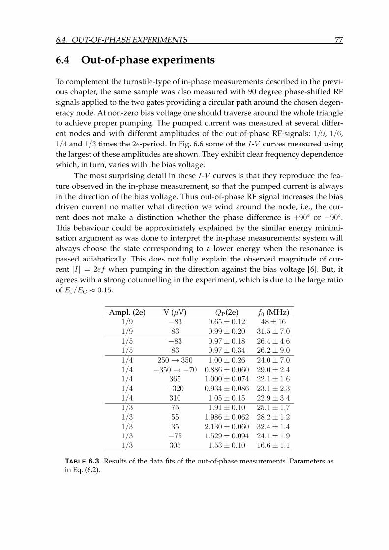
6.4. OUT-OF-PHASE EXPERIMENTS 77
6.4 Out-of-phase experiments
To complement the turnstile-type of in-phase measurements described in the previ-ous chapter, the same sample was also measured with 90 degree phase-shifted RFsignals applied to the two gates providing a circular path around the chosen degen-eracy node. At non-zero bias voltage one should traverse around the whole triangleto achieve proper pumping. The pumped current was measured at several differ-ent nodes and with different amplitudes of the out-of-phase RF-signals: 1/9, 1/6,1/4 and 1/3 times the 2e-period. In Fig. 6.6 some of the I-V curves measured usingthe largest of these amplitudes are shown. They exhibit clear frequency dependencewhich, in turn, varies with the bias voltage.
The most surprising detail in these I-V curves is that they reproduce the fea-ture observed in the in-phase measurement, so that the pumped current is alwaysin the direction of the bias voltage. Thus out-of-phase RF signal increases the biasdriven current no matter what direction we wind around the node, i.e., the cur-rent does not make a distinction whether the phase difference is +90 or −90.This behaviour could be approximately explained by the similar energy minimi-sation argument as was done to interpret the in-phase measurements: system willalways choose the state corresponding to a lower energy when the resonance ispassed adiabatically. This does not fully explain the observed magnitude of cur-rent |I| = 2ef when pumping in the direction against the bias voltage [6]. But, itagrees with a strong cotunnelling in the experiment, which is due to the large ratioof EJ/EC ≈ 0.15.
Ampl. (2e) V (µV) QP(2e) f0 (MHz)1/9 −83 0.65± 0.12 48± 161/9 83 0.99± 0.20 31.5± 7.01/5 −83 0.97± 0.18 26.4± 4.61/5 83 0.97± 0.34 26.2± 9.01/4 250 → 350 1.00± 0.26 24.0± 7.01/4 −350 → −70 0.886± 0.060 29.0± 2.41/4 365 1.000± 0.074 22.1± 1.61/4 −320 0.934± 0.086 23.1± 2.31/4 310 1.05± 0.15 22.9± 3.41/3 75 1.91± 0.10 25.1± 1.71/3 55 1.986± 0.062 28.2± 1.21/3 35 2.130± 0.060 32.4± 1.41/3 −75 1.529± 0.094 24.1± 1.91/3 305 1.53± 0.10 16.6± 1.1
TABLE 6.3 Results of the data fits of the out-of-phase measurements. Parameters asin Eq. (6.2).
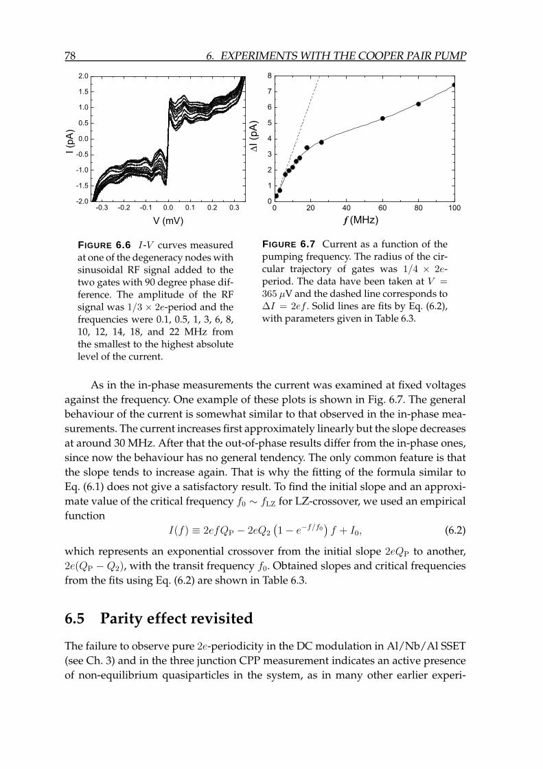
78 6. EXPERIMENTS WITH THE COOPER PAIR PUMP
FIGURE 6.6 I-V curves measuredat one of the degeneracy nodes withsinusoidal RF signal added to thetwo gates with 90 degree phase dif-ference. The amplitude of the RFsignal was 1/3 × 2e-period and thefrequencies were 0.1, 0.5, 1, 3, 6, 8,10, 12, 14, 18, and 22 MHz fromthe smallest to the highest absolutelevel of the current.
FIGURE 6.7 Current as a function of thepumping frequency. The radius of the cir-cular trajectory of gates was 1/4 × 2e-period. The data have been taken at V =365 µV and the dashed line corresponds to∆I = 2ef . Solid lines are fits by Eq. (6.2),with parameters given in Table 6.3.
As in the in-phase measurements the current was examined at fixed voltagesagainst the frequency. One example of these plots is shown in Fig. 6.7. The generalbehaviour of the current is somewhat similar to that observed in the in-phase mea-surements. The current increases first approximately linearly but the slope decreasesat around 30 MHz. After that the out-of-phase results differ from the in-phase ones,since now the behaviour has no general tendency. The only common feature is thatthe slope tends to increase again. That is why the fitting of the formula similar toEq. (6.1) does not give a satisfactory result. To find the initial slope and an approxi-mate value of the critical frequency f0 ∼ fLZ for LZ-crossover, we used an empiricalfunction
I(f) ≡ 2efQP − 2eQ2
(1− e−f/f0
)f + I0, (6.2)
which represents an exponential crossover from the initial slope 2eQP to another,2e(QP − Q2), with the transit frequency f0. Obtained slopes and critical frequenciesfrom the fits using Eq. (6.2) are shown in Table 6.3.
6.5 Parity effect revisited
The failure to observe pure 2e-periodicity in the DC modulation in Al/Nb/Al SSET(see Ch. 3) and in the three junction CPP measurement indicates an active presenceof non-equilibrium quasiparticles in the system, as in many other earlier experi-
6.5. PARITY EFFECT REVISITED 79
ments [62, 64, 90, 135]. In the case of Al/Al/Al SSET and the CPB the quasiparticletraps included in the biasing lines improved the situation and pure 2e-periodicitywas observed in many samples (see Ch. 2.3.1). Nevertheless, these traps had no ef-fect in the measurements of the CPP, which could be the case due to the extra middlejunction not connected to any trap directly. Pure 2e-periodicity has been observedin the similar structure, but with the middle junction much more transparent com-pared to outer ones, thus turning the configuration towards the SSET [28].
In the experiments with Al/Nb/Al SSET the quasiparticle traps were not in-cluded since all the extra fabrication steps were removed not to intrude the sensitivefabrication process of niobium, and since the layout of the device clearly fulfilled thedemand for the robust 2e-periodicity stated in [11]. Obviously these requirementswere not enough and it is not clear that the use of Nb would improve the parity ef-fect in any device. The reason for the lack of the parity effect in Nb based structurescould be the subgap quasiparticle states, which are, e.g., due to depairing effect orthe granularity of the Nb-film inducing variations in ∆Nb.
If one assumes that there is always some extra undesirable subgap quasiparti-cle states in the samples, then the tunnelling rate of the quasiparticles, Γ would beessentially determined by the charging energy and the general golden rule expres-sion in the limit EC kBT : Γ ≈ EC/(e
2R∗T) exp(−EC/kBT ), where R∗T = RT/η2 and
η ' 10−4 is the relative density of quasiparticle states inside the gap [47, 110]. Withparameters corresponding to the sample used in the measurement of the CPP andwith temperature of 30 mK, this yields ∼ 1055 hours for the average time betweenthe quasiparticle tunnelling, which is infinite in the time scale of the measurements.Yet, this time depends strongly on the temperature and if the electronic temperatureof the sample would be higher, e.g., 300 mK, which could be the case due to inad-equate filtering or thermalisation of the measurement lines, the time between thequasiparticle tunnelling events would be ∼500 ms resulting in e-periodicity in themeasurement. This argument yields the same threshold temperature of∼250 mK for2e-periodicity as the earlier measurements in [80], [89] and [126], and could explainwhy the 2e-periodicity is sometimes seen and sometimes not, even if the sampleparameters would suggest clear parity effect.

80 6. EXPERIMENTS WITH THE COOPER PAIR PUMP
7 Conclusion
In this thesis a quantitative theory of adiabatic Cooper pair transport in one-dimen-sional arrays of Josephson junctions in an environment with vanishing impedance,has been developed. The theory predicts, among other things, that the quantum in-accuracy of the Cooper pair pumping in arrays with a small number of junctions isvery large. The effects due to inhomogeneous arrays or nonideal gating sequencesare also quantitatively treated. The theoretical predictions have been verified bynumerical calculations, but whether the model is realistic enough to give quanti-tatively, or at least qualitatively, correct results will be ultimately tested in experi-ments.
A method to quantitatively estimate the decoherence time, τϕ, due to dissi-pative electromagnetic environment in circuits consisting of small Josephson junc-tions has been presented. This method allows discussion about the suitability ofthe system in consideration as a quantum bit. Also a direct measurement of τϕ asa crossover between coherent and incoherent pumping in the single Cooper pairpump is suggested. It is also shown explicitly how the pumped charge in the Cooperpair pump can be understood as a partial derivative of Berry’s phase with respect tothe phase difference ϕ across the array. This makes it possible to obtain informationabout Berry’s phase by measuring the pumped current in the CPP.
The experiments with Nb/AlOx/Al SSETs show that Nb based junctions withhigh critical temperature (Tc ≈ 8.5 K) and Josephson coupling, can be fabricated us-ing the regular self-alignment technique. The measured Al/Nb/Al SSETs show theclear signature of the resonant tunnelling of Cooper pairs combined with the elasticcotunnelling of quasiparticles, q-MQT, through the barrier of ∆Nb. Also a qualitativeexplanation is given for the smeared I-V characteristics of the Nb junctions.
In experiments with Cooper pair pump the current in both the in-phase andout-of-phase gate cycles follows the relation ∆I = 2ef in data measured with am-plitudes crossing only one triangle on the gate plane. No effect due to coherence in-duced inaccuracy could be determined due to the fast decoherence induced by roomtemperature equipment in the biasing circuit. These experiments demonstrate, how-ever, in practise how a Cooper pair pump could be used as a turnstile with help ofdissipation. A model was developed to explain the process and experiments clearlydemonstrated this behaviour also quantitatively.
The accuracy of the turnstile-kind of behaviour in the in-phase measurement ofthe CPP is contradicting the e-periodicity observed in the DC-modulation measure-
81
82 7. CONCLUSION
ment induced by the stochastic tunnelling of quasiparticles. To explain this twofoldbehavior of the system, a very general principle of a system to always strive for min-imum energy was used. The model also agrees with the earlier measurements of theCooper pair pump [64, 135] and similar devices [94].
According to experiments we state that it is very unlikely for a Cooper pairpump as such to be able to provide a current standard or otherwise work with highaccuracy. The strong cotunnelling and relaxation among other uncontrollable pro-cesses tend to degrade the pumping cycles. Also the use of the CPP to measure, e.g.,decoherence time would need a much more controlled electromagnetic environmentto be successful [4, 55]. However, there may be ways such as highly resistive envi-ronment [135] or the use of combined flux and charge control [104,112], to overcomethese difficulties.
Bibliography
[1] This thesis article A.I.
[2] This thesis article A.II.
[3] This thesis article A.III.
[4] This thesis article A.IV.
[5] This thesis article A.V.
[6] This thesis article A.VI.
[7] This thesis article A.VII.
[8] AMBEGAOKAR, V. AND BARATOFF, A., Tunneling Between Superconductors.Phys. Rev. Lett. 10 (1963) 486. ; erratum, 11 (1963) 104.
[9] ANDERSSON, K., DELSING, P., AND HAVILAND, D., Synchronous Cooper pairtunneling in a 1D array of Josephson junctions. Phys. B 248-288 (2000) 1816.
[10] AO, P. AND RAMMER, J., Quantum Dynamics of a two-state system in a dissipativeenvironment. Phys. Rev. B 43 (1991) 5397.
[11] AUMENTADO, J., KELLER, M. W., AND MARTINIS, J. M., Requirements for ro-bust 2e periodicity in single-Cooper-pair transistors (2002). Submitted to J. Phys.Soc. Jpn. (cond-mat/0308253).
[12] AUNOLA, M., Analysis of the tunnelling-charging Hamiltonian of a Cooper pairpump, Ph.D. thesis, Department of Physics, University of Jyväskylä (2001).
[13] AUNOLA, M., Tunneling-charging Hamiltonian of a Cooper-pair pump.Phys. Rev. B 63 (2001) 132508.
[14] AVERIN, D. V., Adiabatic quantum computation with Cooper pairs. Solid StateCommun. 105 (1998) 659.
83
84 BIBLIOGRAPHY
[15] AVERIN, D. V., Continuous weak measurement of the macroscopic quantum co-herent oscillations, in Exploring the quantum-classical frontier, edited by J. R.Friedman and S. Han (Nova science publishers, Commack, NY, 2000). Cond-mat/0004364.
[16] AVERIN, D. V. AND ALESHKIN, V. YA., Pis’ma Zh. Éksp. Teor. Fiz. 50 (1989)331. [JETP Lett. 50, 367 (1989)].
[17] AVERIN, D. V. AND LIKHAREV, K. K., Modern problems in condensed mattersciences, in Mesoscopic phenomena in solids, edited by B. L. Altschuler, P. A. Lee,and R. A. Webb (North-Holland, Amsterdam, 1991), p. 213.
[18] AVERIN, D. V. AND ODINTSOV, A. A., Macroscopic quantum tunneling of theelectric charge in small tunnel junctions. Phys. Lett. A 140 (1989) 251.
[19] AVERIN, D. V., ODINTSOV, A. A., AND VYSHENSKII, S. V., Ultimate accuracyof single-electron dc current standards. J. Appl. Phys. 73 (1993) 1297.
[20] AVERIN, D. V. AND NAZAROV, YU. V., Virtual electron diffusion during quantumtunneling of the electric charge. Phys. Rev. Lett. 65 (1990) 2446.
[21] AVERIN, D. V. AND NAZAROV, YU. V., Macroscopic Quantum Tunneling ofCharge and Co-Tunneling, in Single charge tunnelling, Coulomb blockade phenom-ena in nanostructures, edited by H. Grabert and M. H. Devoret (Plenum, NewYork, 1992), p. 217.
[22] AVERIN, D. V. AND NAZAROV, YU. V., Single-Electron Charging of a supercon-ducting Island. Phys. Rev. Lett. 69 (1992) 1993.
[23] BARDEEN, J., COOPER, L. N., AND SCHRIEFFER, J. R., Theory of Superconduc-tivity. Phys. Rev. 108 (1957) 1175.
[24] BENNETT, C. H., BRASSARD, G., CRÉPEAU, C., JOZSA, R., PERES, A., AND
WOOTTERS, W. K., Teleporting an unknown quantum state via dual classical andEinstein-Podolsky-Rosen channels. Phys. Rev. Lett. 70 (1993) 1895.
[25] BENNETT, C. H. AND DIVINCENZO, D. P., Towards an engineering era? Nature377 (1995) 389.
[26] BENNETT, C. H. AND DIVINCENZO, D. P., Quantum information and Computa-tion. Nature 404 (2000) 247.
[27] BERRY, M. V., Quantal phase factors accompanying adiabatic changes. Proc. R. Soc.London, Ser. A 392 (1984) 45.
[28] BIBOW, E., LAFARGE, P., AND LÉVY, L. P., Resonant Cooper Pair Tunnelingthrough a Double-Island Qubit. Phys. Rev. Lett. 88 (2002) 017003.
BIBLIOGRAPHY 85
[29] BIBOW, E. N., Spectroscopie tunnel d’un circuit a deux i lots, Ph.D. thesis, del’Université Joseph Fourier - Grenoble I en Physique (2001).
[30] BOUCHIAT, V., VION, D., JOYEZ, P., ESTEVE, D., AND DEVORET, M. H., Quan-tum Coherence with a Single Cooper Pair. Physica Scripta T 76 (1998) 165.
[31] BOUCHIAT, V., VION, D., JOYEZ, P., ESTEVE, D., AND DEVORET, M. H., Quan-tum Coherence of Charge States in the Single Electron Box. J. Supercond. 12 (1999)789.
[32] BRATUS, E. N., SHUMEIKO, V. S., AND WENDIN, G., Theory of SubharmonicGap Structure in Superconducting Mesoscopic Tunnel Contacts. Phys. Rev. Lett. 74(1995) 2110.
[33] VAN DEN BRINK, A. M., ODINTSOV, A. A., BOBBERT, P. A., AND SCHoN, G.,Coherent Cooper pair tunneling in systems of Josephson junctions: effects of quasipar-ticle tunneling and of the electromagnetic environment. Z. Phys. B 85 (1991) 459.
[34] CALDEIRA, A. O. AND LEGGETT, A. J., Quantum tunnelling in a dissipative sys-tem. Ann. Phys. 149 (1983) 374.
[35] CHIORESCU, I., NAKAMURA, Y., HARMANS, C. J. P. M., AND MOOIJ, J. E.,Coherent Quantum Dynamics of a Superconducting Flux Qubit. Science 299 (2003)1869.
[36] CHOI, M. S., FAZIO, R., SIEWERT, J., AND BRUDER, C., Coherent oscillations ina Cooper pair box. Europhys. Lett. 53 (2001) 251.
[37] COTTET, A. Private communication.
[38] DELAHAYE, J., HASSEL, J., LINDELL, R., SILLANPÄÄ, M., PAALANEN, M.,SEPPÄ, H., AND HAKONEN, P., Low-Noise Current Amplifier Based on Meso-scopic Josephson Junction. Science 299 (2003) 1045.
[39] DEVORET, M. H., ESTEVE, D., GRABERT, H., INGOLD, G.-L., POTHIER, H.,AND URBINA, C., Effect of the electromagnetic environment on the Coulomb block-ade in ultrasmall tunnel junctions. Phys. Rev. Lett. 64 (1990) 1824.
[40] DEVORET, M. H., ESTEVE, D., AND URBINA, C., Single-electron Transfer inMetallic Nanostructures. Nature 360 (1992) 547.
[41] DEVORET, M. H. AND SCHOELKOPF, R. J., Amplifying Quantum Signals withthe Single-Electron Transistor. Nature 406 (2000) 1039.
[42] DIEKS, D., Communication by EPR devices. Phys. Lett. A 92 (1982) 271.
86 BIBLIOGRAPHY
[43] DOLAN, G. J., Offset masks for lift-off photoprocessing. Appl. Phys. Lett. 31 (1977)337.
[44] DOLATA, R., SCHRERER, H., ZORIN, A. B., AND NIEMEYER, J., Single electrontransistors with high-quality superconducting niobium island. Appl. Phys. Lett. 80(2002) 2776.
[45] DUBOS, P., CHARLAT, P., CROZES, T., PANIEZ, P., AND PANNETIER, B., Ther-mostable trilayer resist for niobium lift-off. J. Vac. Sci. Technol. B 18 (2000) 122.
[46] DYNES, R. C., Direct Measurement of Quasiparticle-Lifetime Broadening in aStrong-Coupled Superconductor. Phys. Rev. Lett. 41 (1978) 1509.
[47] DYNES, R. C. AND GARNO, J. P., Tunneling Study of Superconductivity near theMetal-insulator Transition. Phys. Rev. Lett. 53 (1984) 2437.
[48] EILES, T. M., MARTINIS, J. M., AND DEVORET, M. H., Even-Odd Asym-metry of a Superconductor Revealed by Coulomb Blockade of Andreev Reflection.Phys. Rev. Lett. 70 (1993) 1862.
[49] VAN ENK, S. J., CIRAC, J. I., AND ZOLLER, P., Ideal Quantum Communica-tion over Noisy Channels: A Quantum Optical Implementation. Phys. Rev. Lett.78 (1997) 4293.
[50] VAN ENK, S. J., KIMBLE, H. J., CIRAC, J. I., AND ZOLLER, P., Quantum com-munication with dark photons. Phys. Rev. A 59 (1999) 2659.
[51] ESTEVE, D., Transferring Electrons One by One, in Single charge tunnelling,Coulomb blockade phenomena in nanostructures, edited by H. Grabert and M. H.Devoret (Plenum, New York, 1992), p. 109.
[52] FALCI, G., FAZIO, R., PALMA, G. H., SIEWERT, J., AND VEDRAL, V., Detectionof geometric phases in superconducting nanocircuits. Nature 407 (2000) 355.
[53] FARHANGFAR, SH., MANNINEN, A. J., AND PEKOLA, J. P., Effect of the electro-magnetic environment on arrays of small normal metal tunnel junctions: Numericaland experimental investigation. Europhys. Lett. 49 (2000) 237.
[54] FARHANGFAR, SH., HIRVI, K. P., KAUPPINEN, J. P., PEKOLA, J. P., TOPPARI,J. J., AVERIN, D. V., AND KOROTKOV, A. N., One Dimensional Arrays and Soli-tary Tunnel Junctions in the Weak Coulomb Blockade Regime: CBT Thermometry.J. Low Temp. Phys. 108 (1997) 191.
[55] FAZIO, R., HEKKING, F. W. J., AND PEKOLA, J. P., Measurement of coherenttransfer in an adiabatic Cooper pair pump. Phys. Rev. B 68 (2003) 054510.
BIBLIOGRAPHY 87
[56] FILE, J. AND MILLS, R. G., Observation of Persistent Current in a SuperconductingSolenoid. Phys. Rev. Lett. 10 (1963) 93.
[57] FITZGERALD, R. J., POHLEN, S. L., AND TINKHAM, M., Observation of Andreevreflection in all-superconducting single-electron transistor. Phys. Rev. B 57 (1998)R11073.
[58] FONSECA, L. R. C., KOROTKOV, A. N., AND LIKHAREV, K. K., Accu-racy of the single-electron pump using an optimized step-like rf drive waveform.Appl. Phys. Lett. 69 (1996) 1858.
[59] FRIEDMAN, J. R., PATEL, V., CHEN, W., TOLPYGO, S. K., AND LUKENS, J. E.,Quantum superposition of distinct macroscopic states. Nature 406 (2000) 43.
[60] FULTON, T. A. AND DOLAN, G. J., Observation of single-electron charging effectsin small tunnel junctions. Phys. Rev. Lett. 59 (1987) 109.
[61] FULTON, T. A., GAMMEL, P. L., BISHOP, D. J., DUNKLEBERGER, L. N., AND
DOLAN, G. J., Observation of combined Josephson and charging effects in smalltunnel junction circuits. Phys. Rev. Lett. 63 (1989) 1307.
[62] GEERLIGS, L. J., ANDEREGG, V. F., ROMIJN, J., AND MOOIJ, J. E., SingleCooper pair tunneling in small-capacitance junctions. Phys. Rev. Lett. 65 (1990)377.
[63] GEERLIGS, L. J., AVERIN, D. V., AND MOOIJ, J. E., Observation of macroscopicquantum tunneling through the Coulomb energy barrier. Phys. Rev. Lett. 65 (1990)3037.
[64] GEERLIGS, L. J., VERBRUGH, S. M., HADLEY, P., MOOIJ, J. E., POTHIER, H.,LAFARGE, P., URBINA, C., ESTEVE, D., AND DEVORET, M. H., Single Cooperpair pump. Z. Phys. B 85 (1991) 349.
[65] GINZBURG, V. L. AND LANDAU, L. D., Teorii sverchhprovodimosti.Zh. Eks. Teor. Fiz. 20 (1950) 1064.
[66] GLAUBER, R., in Lectures in Theoretical Physics, edited by A. O. Barut and W. E.Brittin (Interscience, New York, 1956).
[67] GLAZMAN, L. I. AND MATVEEV, K. A., Residual quantum conductivity underCoulomb-blockade conditions. Pis’ma Zh. Eksp. Teor. Phys. 51 (1990) 425. [JETPLett. 51 (1990) 484].
[68] GOLUBEV, D. S. AND ZAIKIN, A. D., Quantum Physics at Mesoscopic Scale(Frontieres, 1999).
88 BIBLIOGRAPHY
[69] GRABERT, H., INGOLD, G.-L., DEVORET, M. H., ESTEVE, D., POTHIER,H., AND URBINA, C., Single electron tunnelin rates in multijunction circuits.Z. Phys. B: Condens. Matter 84 (1991) 143.
[70] GROVER, L. K., Quantum Mechanics Helps in Searching for a Needle in a Haystack.Phys. Rev. Lett. 79 (1997) 325.
[71] HADLEY, P., DELVIGNE, E., VISSCHER, E. H., LaHTEENMaKI, S., AND MOOIJ,J. E., 3e tunneling processes in a superconducting single-electron tunneling transis-tor. Phys. Rev. B 58 (1998) 15317.
[72] HARADA, Y., HAVILAND, D. B., DELSING, P., CHEN, C. D., AND CLAESSON,T., Fabrication and measurement of a Nb based superconducting single electron tran-sistor. Appl. Phys. Lett. 65 (1994) 636.
[73] HAROCHE, S., BRUNE, M., AND RAIMOND, J. M., Experiments withsingle atoms in a cavity: entanglement, Schrödinger’s cats and decoherence.Phil. Trans. (R. Soc. Lond.) A 355 (1997) 2367.
[74] HASSEL, J., SEPPÄ, H., AND KIVIRANTA, M., A new way to realize a pro-grammable Josephson voltage standard. Phys. B 284-288 (2000) 2073.
[75] HASSELBERG, L.-E., LEVINSEN, M. T., AND SAMUELSEN, M. R., Theories ofsubharmonic gap structures in superconducting junctions. Phys. Rev. B 9 (1974)3757.
[76] HAVILAND, D. B., HARADA, Y., DELSING, P., CHEN, C. D., AND CLAESON,T., Observation of Resonant Tunneling of Cooper pairs. Phys. Rev. Lett. 73 (1993)1541.
[77] INGOLD, G.-L. AND NAZAROV, YU. V., Charge Tunneling Rates in UltrasmallJunctions, in Single charge tunnelling, Coulomb blockade phenomena in nanostruc-tures, edited by H. Grabert and M. H. Devoret (Plenum, New York, 1992), p. 21.
[78] JENSEN, H. D. AND MARTINIS, J. M., Accuracy of the electron pump.Phys. Rev. B 46 (1992) 13407.
[79] JOSEPHSON, B. D., Possible new effects in superconductive tunnelling. Phys. Lett.1 (1962) 251.
[80] JOYEZ, P., LAFARGE, P., FILIPE, A., ESTEVE, D., AND DEVORET, M. H., Obser-vation of parity-induced suppression of Josephson tunneling in the superconductingsingle electron transistor. Phys. Rev. Lett. 72 (1994) 2458.
[81] KELLER, M. W., MARTINIS, J. M., AND KAUTZ, R. L., Rare Errors ina Well-Characterized Electron Pump: Comparison of Experiment and Theory.Phys. Rev. Lett. (1998) 4530.
BIBLIOGRAPHY 89
[82] KELLER, M. W., MARTINIS, J. M., ZIMMERMAN, N. N., AND STEIN-BACH, A. H., Accuracy of electron counting using a 7-junction electron pump.Appl. Phys. Lett. 69 (1996) 1804.
[83] KIM, N., HANSEN, K., TOPPARI, J. J., SUPPULA, T., AND PEKOLA, J. P., Fab-rication of mesoscopic superconducting Nb wires using conventional electron-beamlithographic techniques. J. Vac. Sci. Technol. B 20 (2002) 386.
[84] KLEINSASSER, A. W., MILLER, R. E., MALLISON, W. H., AND ARNOLD,G. B., Observation of Multiple Andreev Reflections in Superconducting Tunnel Junc-tions. Phys. Rev. Lett. 72 (1994) 1738.
[85] KOUWENHOVEN, L. P., JOHNSON, A. T., VAN DER VAART, N. C., HARMANS,C. J. P. M., AND FOXON, C. T., Quantized current in a quantum-dot turnstileusing oscillating tunnel barriers. Phys. Rev. Lett. 67 (1991) 1626.
[86] KUBO, R., The fluctuation-dissipation theorem. Rep. Prog. Phys. 29 (1966) 255.
[87] KUZMIN, L. S., DELSING, P., CLAESON, T., AND LIKHAREV, K. K., Single-electron charging effects in one-dimensional arrays of ultrasmall tunnel junctions.Phys. Rev. Lett. 62 (1989) 2539.
[88] LAFARGE, P., Macroscopic Charge Quantization in Metallic Nanostructures, Ph.D.thesis, Université Paris 6 (1993).
[89] LAFARGE, P., JOYEZ, P., ESTEVE, D., URBINA, C., AND DEVORET, M. H., 2e-Quantization of the Charge on a Superconductor. Nature 365 (1993) 422.
[90] LAFARGE, P., POTHIER, H., WILLIAMS, E. R., ESTEVE, D., URBINA, C., AND
DEVORET, M. H., Direct observation of macroscopic charge quantization. Z. Phys. B85 (1991) 327.
[91] LEGGETT, A. J., Change and Matter (North-Holland, Amsterdam, 1987).
[92] LIKHAREV, K. K. AND ZORIN, A. B., Theory of the Bloch-Wave Oscillations inSmall Josephson Junctions. J. Low Temp. Phys. 59 (1985) 347.
[93] LOTKHOV, S. V., BOGOSLOVSKY, S. A., ZORIN, A. B., AND NIEMEYER, J.,Cooper pair cotunneling in single charge transistors with dissipative electromagneticenvironment. Cond-mat/0305113 (unpublished).
[94] LOTKHOV, S. V., BOGOSLOVSKY, S. A., ZORIN, A. B., AND NIEMEYER, J.,Frequency-Locked Current of Cooper pairs in Superconducting Single Electron Tran-sistor with Ohmic Resistor, in International Workshop on Superconducting Nano-Electronics Devices, edited by J. P. Pekola, B. Ruggiero, and P. Silvestrini, SNED(Plenum, Naples, Italy, 2001), p. 105.
90 BIBLIOGRAPHY
[95] MAKHLIN, Y., SCHÖN, G., AND SHNIRMAN, A., Josehpson junction qubits withcontrolled couplings. Nature 386 (1999) 305.
[96] MAKHLIN, Y., SCHÖN, G., AND SHNIRMAN, A., Quantum-state engineeringwith Josephson junction devices. Rev. Mod. Phys. 73 (2001) 357.
[97] MARTINIS, J. M., NAHUM, M., AND JENSEN, H. D., Metrological accuracy ofthe electron pump. Phys. Rev. Lett. 72 (1994) 904.
[98] MEISSNER, W. AND OCHSENFELD, R., Ein neuer Effekt bei Eintritt der Supraleit-fähigkeit. Naturwissenschaften 21 (1933) 787.
[99] MINEEV, V. P. AND SAMOKHIN, K. V., Introduction to Unconventional Supercon-ductors (Gordon and Breach, 1999).
[100] NAKAHARA, M., Geometry, topology, and physics (IOP Publishing, Bristol, NewYork, 1990), pp. 29–30, 364–372.
[101] NAKAMURA, Y., CHEN, C. D., AND TSAI, J. S., Quantitative analysisof Josephson-quasiparticle current in superconducting single-electron transistors.Phys. Rev. B 53 (1996) 8234.
[102] NAKAMURA, Y., PASHKIN, Y. A., AND TSAI, J. S., Coherent control of macro-scopic quantum states in a single-Cooper pair box. Nature 398 (1999) 786.
[103] NAVEH, Y., PATEL, V., AVERIN, D. V., KIKHAREV, K. K., AND LUKENS, J. E.,Universal Distribution of Transparencies in Highly Conductive Nb/AlOx/Nb Junc-tions. Phys. Rev. Lett. 85 (2000) 5404.
[104] NISKANEN, A. O., PEKOLA, J. P., AND SEPPa, H., Fast and Accurate Single-Island Charge Pump: Implementation of a Cooper Pair Pump. Phys. Rev. Lett. 91(2003) 177003.
[105] ONNES, H. K., The resistance of pure mercury at helium temperatures. LeidenComm. 120b (1911).
[106] ONNES, H. K., The disappearance of the resistivity of mercury. Leiden Comm.122b (1911).
[107] ONNES, H. K., On the sudden change in the rate at which the resistance of mercurydisappears. Leiden Comm. 124c (1911).
[108] ORLANDO, T. P., MOOIJ, J. E., TIAN, L., VAN DER VAL, C. H., LEVITOV, L.,AND LLOYD, S., Superconducting persistent-current qubit. Phys. Rev. B. 60 (1999)15398.
BIBLIOGRAPHY 91
[109] PAVOLOTSKY, A. B., WEIMANN, T., SCHERER, H., KRUPENIN, V. A.,NIEMEYER, J., AND ZORIN, A. B., Multilayer technique developed for fabricatingNb-based single-electron devices. J. Vac. Sci. Technol. B 17 (1999) 230.
[110] PEKOLA, J. P., HEIKKILÄ, T. T., SAVIN, A. M., FLYKTMAN, J. T., GIAZOTTO,F., AND HEKKING, F. W. J., Limitations in electron cooling (2003). Submitted.
[111] POTHIER, H., LAFARGE, P., ORFILA, P. F., URBINA, C., ESTEVE, D., AND DE-VORET, M. H., Single electron pump fabricated with ultrasmall normal tunnel junc-tions. Physica B 169 (1991) 573. [Europhys. Lett. 17, 249 (1992)].
[112] ROMITO, A., PLASTINA, F., AND FAZIO, R., Decoherence in a Cooper pair shuttle(2002). Cond-mat/0212414.
[113] SCHOELKOPF, R. J., WAHLGREN, P., KOZHEVNIKOV, A. A., DELSING, P.,AND PROBER, D. E., The Radio-Frequency Single-Electron Transistor (RF-SET):A Fast and Ultrasensitive Electrometer. Science 280 (1998) 1238.
[114] SCHRIEFFER, J. R. AND WILKINS, J. W., Two-particle tunneling processes betweensuperconductors. Phys. Rev. Lett. 10 (1963) 17.
[115] SHILTON, J. M., TALYANSKII, V. I., PEPPER, M., RITCHIE, D. A., FROST,J. E. F., FORD, C. J. B., SMITH, C. G., AND JONES, G. A. C., High-frequencysingle-electron transport in a quasi-one-dimensional GaAs channel induced by sur-face acoustic waves. J. Phys. Cond. Matter 8 (1996) L531.
[116] SHNIRMAN, A. AND SCHÖN, G., Quantum measurement Performed with Single-Electron Transistor. Phys. Rev. B 57 (1998) 15400.
[117] SHNIRMAN, A., SCHÖN, G., AND HERMON, Z., Quantum Manipulations ofSmall Josephson Junctions. Phys. Rev. Lett. 79 (1997) 2371.
[118] SHOR, P. W., Polynomial-time algorithms for prime factorization and discrete loga-rithms on a quantum computer, in Proc. of the 35th Annual Symp. on the Founda-tions of Computer Science (IEEE Computer Society Press, Los Alamitos, Califor-nia, 1994), p. 124. (revised version 1995a Preprint quant-ph/9508027).
[119] SIMON, B., Holonomy, the Quantum adiabatic theorem, and Berry’s phase. Phys.Rev. Lett. 51 (1983) 2167.
[120] STEANE, A., Quantum Computing. Rep. Prog. Phys. 61 (1998) 117.
[121] TALYANSKII, V. I., SHILTON, J. M., PEPPER, M., SMITH, C. G., FORD, C. J. B.,LINFIELD, E. H., RITCHIE, D. A., AND JONES, G. A. C., Single-electrontransport in a one-dimensional channel by high-frequency surface acoustic waves.Phys. Rev. B 56 (1997) 15180.
92 BIBLIOGRAPHY
[122] THOULESS, D. J., Quantization of particle transport. Phys. Rev. B 27 (1983) 6083.
[123] TINKHAM, M., Introduction to superconductivity, 2nd ed. (McGraw-Hill, NewYork, 1996), pp. 257–277.
[124] TINKHAM, M., HERGENROTHER, J. M., AND LU, J. G., Temperature dependenceof even-odd electron-number effects in the single-electron transistor with a supercon-ducting island. Phys. Rev. B 51 (1995) 12649.
[125] TOPPARI, J. J., Sähkömagneettisen ympäristön vaikutus tunnelointiin metalli-sissa nanorakenteissa, Master’s thesis, Department of Physics, University ofJyväskylä (1997).
[126] TUOMINEN, M. T., HERGENROTHER, J. M., TIGHE, T. S., AND TINKHAM, M.,Experimental Evidence for Parity-Based 2e Periodicity in a Superconducting Single-Electron Transistor. Phys. Rev. Lett. 69 (1992) 1997.
[127] TURCHETTE, Q. A., WOOD, C. S., KING, B. E., MYATT, C. J., LEIBFRIED, D.,ITANO, W. M., MONROE, C., AND WINELAND, D. J., Deterministic Entangle-ment of Two Trapped Ions. Phys. Rev. Lett. 81 (1998) 3631.
[128] VION, D., AASSIME, A., COTTET, A., JOYEZ, P., POTHIER, H., URBINA, C.,ESTEVE, D., AND DEVORET, M. H., Manipulating the Quantum State of an Elec-trical Circuit. Science 296 (2002) 886.
[129] VION, D., ORFILA, P. F., JOYEZ, P., ESTEVE, D., AND DEVORET, M. H., Minia-ture electrical filters for single electron devices. J. Appl. Phys. 77 (1995) 2519.
[130] VOLLHARDT, D. AND WoLFLE, P., The Superfluid Phases of 3He (Taylor andFrancis, 1990).
[131] VAN DER WAL, C. H., TER HAAR, A. C. J., WILHELM, F. K., SCHOUTEN,R. N., HARMANS, C. J. P. M., AND MOOIJ, J. E., Quantum Superposition ofMacroscopic Persistent-Current States. Science 290 (2000) 773.
[132] WOOTTERS, W. K. AND ZUREK, W. H., A single Quantum Cannot be Clone.Nature 299 (1982) 802.
[133] ZIMAN, J. M., Principles of the Theory of Solids (Cambridge University Press,Cambridge, England, 1964).
[134] ZORIN, A. B., The Thermocoax cable as the microwave frequency filter for singleelectron circuits. Rev. Sci. Instrum. 66 (1995) 4296.
[135] ZORIN, A. B., BOGOSLOVSKY, S. A., LOTKHOV, S. V., AND NIEMEYER, J.,Cooper pair tunneling in circuits with substantial dissipation: the three-junction R-pump for single Cooper pairs, in Macroscopic Quantum Coherence and Quantum

BIBLIOGRAPHY 93
Computing, edited by D. V. Averin, B. Ruggiero, and P. Silverstrini, MQC2 Insti-tuto Italiano per gli Studi Filosofici (Kluwer Academic / Plenum, New York,2001), p. 147.
[136] ZUREK, W. H., Decoherence and the transition from quantum to classical. PhysicsToday 44 (1991) 36.

94 BIBLIOGRAPHY