Embed Size (px)
Citation preview

Transport phenomena in nanofluidics
Reto B. Schoch*
Microsystems Laboratory, STI-LMIS, École Polytechnique Fédérale de Lausanne (EPFL),CH-1015 Lausanne, Switzerland;Department of Electrical Engineering and Computer Science, Massachusetts Institute ofTechnology, 77 Massachusetts Avenue, Cambridge, Massachusetts 02139, USA;and Department of Biological Engineering, Massachusetts Institute of Technology, 77Massachusetts Avenue, Cambridge, Massachusetts 02139, USA
Jongyoon Han
Department of Electrical Engineering and Computer Science, Massachusetts Institute ofTechnology, 77 Massachusetts Avenue, Cambridge, Massachusetts 02139, USA;and Department of Biological Engineering, Massachusetts Institute of Technology, 77Massachusetts Avenue, Cambridge, Massachusetts 02139, USA
Philippe Renaud
Microsystems Laboratory, STI-LMIS, École Polytechnique Fédérale de Lausanne (EPFL),CH-1015 Lausanne, Switzerland
�Published 17 July 2008�
The transport of fluid in and around nanometer-sized objects with at least one characteristicdimension below 100 nm enables the occurrence of phenomena that are impossible at bigger lengthscales. This research field was only recently termed nanofluidics, but it has deep roots in science andtechnology. Nanofluidics has experienced considerable growth in recent years, as is confirmed bysignificant scientific and practical achievements. This review focuses on the physical properties andoperational mechanisms of the most common structures, such as nanometer-sized openings andnanowires in solution on a chip. Since the surface-to-volume ratio increases with miniaturization, thisratio is high in nanochannels, resulting in surface-charge-governed transport, which allows ionseparation and is described by a comprehensive electrokinetic theory. The charge selectivity is mostpronounced if the Debye screening length is comparable to the smallest dimension of the nanochannelcross section, leading to a predominantly counterion containing nanometer-sized aperture. Theseunique properties contribute to the charge-based partitioning of biomolecules at the micro-channel-nanochannel interface. Additionally, at this free-energy barrier, size-based partitioning can beachieved when biomolecules and nanoconstrictions have similar dimensions. Furthermore, nanoporesand nanowires are rooted in interesting physical concepts, and since these structures demonstratesensitive, label-free, and real-time electrical detection of biomolecules, the technologies hold greatpromise for the life sciences. The purpose of this review is to describe physical mechanisms on thenanometer scale where new phenomena occur, in order to exploit these unique properties and realizeintegrated sample preparation and analysis systems.
DOI: 10.1103/RevModPhys.80.839 PACS number�s�: 47.61.�k, 82.39.Wj, 73.63.�b, 87.85.Rs
CONTENTS
I. Introduction 840
II. Electrokinetic Effects 841
A. Electrostatics in liquids 841
1. Electrical double layer 841
2. Potential distribution in EDL 842
3. Debye-Hückel approximation 842
4. Gouy-Chapman model 843
5. Surface charge density 843
6. Surface conductance 844
7. Continuum models and molecular-dynamics
simulations 844
B. Electrokinetic effects in nanochannels 844
1. Basic physics of electrokinetics 845
2. Comprehensive electrokinetic theory for
nanochannels 846
C. Electrode-electrolyte interface 849
1. Charge-transfer resistance 849
2. Constant phase element 850
III. Phenomena at the Microchannel-Nanochannel
Interface 850
A. Electrical characterization of nanochannels 850
1. Impedance spectroscopy 850
2. Nanochannel conductance 851
3. Ionic current rectification 853
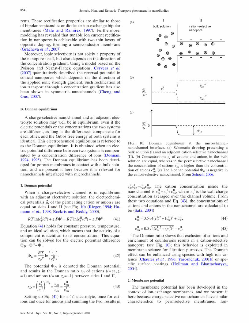
B. Donnan equilibrium 854
*Present address: Department of Mechanical Engineering,Stanford University, Stanford, CA 94305, USA. Author towhom correspondence should be [email protected]
REVIEWS OF MODERN PHYSICS, VOLUME 80, JULY–SEPTEMBER 2008
0034-6861/2008/80�3�/839�45� ©2008 The American Physical Society839

1. Donnan potential 8542. Membrane potential 854
C. Exclusion-enrichment effect 8551. Permselectivity of a nanochannel 8552. Model of the exclusion-enrichment effect 857
D. Partitioning at the interface 8571. Partition coefficient for colloids 8582. Electrostatic sieving of proteins 8583. Active control of partitioning 859
E. Concentration polarization 8601. Limiting current through nanochannels 8602. Electroconvection for mixing 8613. Preconcentration of molecules 862
IV. Macromolecule Separation Mechanisms UsingNanometer-Sized Structures 863A. Entropic trapping 863B. Ogston sieving 863C. Entropic recoil 864D. Anisotropy for continuous-flow separation 864
V. Nanopores and Nanowires for Label-Free BiomoleculeDetection 865A. Biomolecule translocations through nanopores 865
1. Biological nanopores 8662. Synthetic nanopores 8663. Current decrease and increase 867
B. Nanowire sensors 8681. Fabrication techniques 8682. Operation mechanism 8693. Single-molecule sensitivity 8694. Detection efficiency 870
VI. Fabrication of Nanochannels 870A. Wet and dry etching 871B. Sacrificial layer methods 871C. High-energy beam techniques 872D. Nanoimprint lithography 872E. Bonding and sealing methods 872F. Realization of single nanopores in membranes 872
VII. Conclusions and Perspectives 873Acknowledgments 874Lists of Abbreviations and Symbols 874References 875
I. INTRODUCTION
Nanofluidics is defined as the study and application offluid flow in and around nanometer-sized objects with atleast one characteristic dimension below 100 nm �Eijkeland van den Berg, 2005a�. At such length scales, struc-tures have a high surface-to-volume ratio, leading tonew physical phenomena that are not observed at mac-rofluidic or microfluidic size scales �Di Ventra et al.,2004; Han, 2004�. One significant benefit of nanofluidicsis that it presents the possibility of learning new scienceusing controlled regular nanostructures �Mukhopadhyay,2006�, which makes it relevant for many areas in nano-science and nanotechnology.
The term nanofluidics has only recently been intro-duced with the rise of micro total analysis systems��TAS� �Manz et al., 1990�, which aim to integrate allsteps of biochemical analysis on one microchip �Squires
and Quake, 2005; Whitesides, 2006�. The roots of nanof-luidics are broad, and processes on the nanometer scalehave implicitly been studied for decades in chemistry,physics, biology, materials science, and many areas ofengineering. This dynamic new field has drawn attentionin technology, biology, and medicine due to advances inbiomolecule preparation and analysis systems �Lieber,2003�, single-molecule interrogations �Craighead, 2003,2006�, and other unique modes of molecular manipula-tion. For example, molecules can be controlled bycharge in nanochannels because of their electrostatic in-teractions with the electrical double layer �EDL�, ashielding layer that is naturally created within the liquidnear a charged surface. Moreover, size-based filtrationand sieving can be achieved because the length scales ofbiomolecules and synthetic nanometer-sized objects aresimilar.
In this review, we present the following unique prop-erties of nanofluidic systems: nanowires can be operatedas field-effect transistors to detect chemical and biologi-cal species label-free, and transport through nanochan-nels leads to analyte separation and new phenomenawhen the EDL thickness becomes comparable to thesmallest channel opening �Fig. 1�. Such charge-selectivefeatures were first described in membrane filtration �us-ing mainly irregular nanoporous systems�, and industrialapplications have been developed. However, mem-branes are not in the scope of this review, and the readeris referred to the comprehensive literature of membranescience �Helfferich, 1962; Sata, 2004; Strathmann, 2004�.We focus instead on geometrically well-defined, solid-state nanochannels with one cross-sectional dimensionbetween a few nanometers and 100 nm that are manu-factured on a chip with standard microfabrication tech-nology processes. Compared to membranes, which yieldstatistical results, single, well-designed, and controllednanochannels are ideal physical modeling systems tostudy fluidics in a precise manner. Carbon nanotubes arenot covered in this review, and the reader is referred toWhitby and Quirke �2007�.
The authors are inspired by nature’s ultimate nano-fluidic system, namely, transmembrane protein channels.They have remarkable features such as high charge se-lectivity, which was first described in studies of cell-function-controlling potassium channels on the cell
High ionic strength Low ionic strength
FIG. 1. Electrical double layer �EDL, shaded in gray� at highionic strength, it is thin, allowing co-ions and counterions topass through the nanochannel. At low ionic strength, the EDLthickness increases, resulting in a counterion-selectivenanochannel. From Schoch, 2006.
840 Schoch, Han, and Renaud: Transport phenomena in nanofluidics
Rev. Mod. Phys., Vol. 80, No. 3, July–September 2008

membrane. These channels are 10 000 times more per-meable to potassium than to sodium although both at-oms have one positive net charge �Israelachvili, 1992;Doyle et al., 1998�. At the same time, these ion channelsexhibit high transport throughput, approaching the dif-fusional limit. Such a performance has not beenachieved by any artificial nanopore, which demonstratesthat there is much to be learned from biology.
In this review, we first present classic electrostatic andelectrokinetic theory relevant to nanofluidics in Sec. II.Expert readers may focus directly on Sec. II.B.2, whichdescribes electrokinetic effects of nanochannels. When ananochannel is contacted, the geometric size differencebetween the interfacing channel and the nanochannelleads to a free-energy barrier, and the unique propertiesof the microchannel-nanochannel interface are analyzedin Sec. III. Section IV focuses on systems that includenanometer-sized structures for separating biomoleculessuch as DNA and proteins. Then we describe operationmechanisms and physical effects of nanopores and nano-wires for label-free biomolecule detection in Sec. V. Thefabrication techniques of nanometer-sized openings thatwe discuss in this review are summarized in Sec. VI.Finally, we draw conclusions and offer perspectivesabout transport phenomena in nanofluidics.
II. ELECTROKINETIC EFFECTS
Here we introduce the reader to electrostatics in liq-uids and electrokinetic effects, which are the most im-portant and fundamental concepts for the description oftransport in nanofluidics. This classical theory was estab-lished decades ago in well-established disciplines, but itcannot be omitted in the new interdisciplinary field ofnanofluidics �Eijkel and van den Berg, 2005a�, and willtherefore be summarized.
A. Electrostatics in liquids
When considering that a solid in contact with a liquidbears a surface charge, one perceives that this parameteris of increased importance in nanochannels, since theyhave a high surface-to-volume ratio. Surface charge iscaused by the dissociation of surface groups and the spe-cific �nonelectric� adsorption of ions in solution to thesurface �Perram et al., 1973; Behrens and Grier, 2001�.Depending on the number and type of acid and basicgroups present in solution �Hunter and Wright, 1971;Davis et al., 1978; Sonnefeld et al., 1995�, the solid haseither a positive or a negative surface charge density,which is phenomenologically described by �s=�iqi /A,where qi=zie is the net charge of ion i, zi is the valencyof ion i, e is the electron charge, and A is the surfacearea. A typical value of high charge density and fullyionized surfaces is �s=0.3 C m−2, which corresponds toone charge per �0.5 nm2. At a specific pH value of thesolution, the surface bears no net charge; this is knownas the point of zero charge, which is �2 for glass �Parks,
1965; Iler, 1979�. We focus on glass for reasons describedin Sec. VI to do with the fabrication of nanochannels.
Surface charges result in electrostatic forces, whichare important for the description of long-range interac-tions between molecules and surfaces in liquids, andthus they govern transport in nanofluidic systems. Atsmall distances, van der Waals forces contribute to theattractive part of the interaction, for example, betweendissolved particles, whereas coagulation is prevented byrepulsive or attractive electrostatic forces. The interplaybetween van der Waals and electrostatic forces was ini-tially described in the 1940s in the Derjaguin-Landau-Verwey-Overbeek �DLVO� theory �Overbeek, 1952; Is-raelachvili, 1992�, which is important for the descriptionof colloidal stability. van der Waals forces are greatlyinsensitive to variations in electrolyte concentration andpH, which is not true for electrostatic forces.
1. Electrical double layer
Due to the fixed surface charge at the solid interface,an oppositely charged region of counterions develops inthe liquid to maintain the electroneutrality of the solid-liquid interface. This screening region is denoted as theEDL because ideally it consists of opposite charges,some of which are bound while others are mobile.
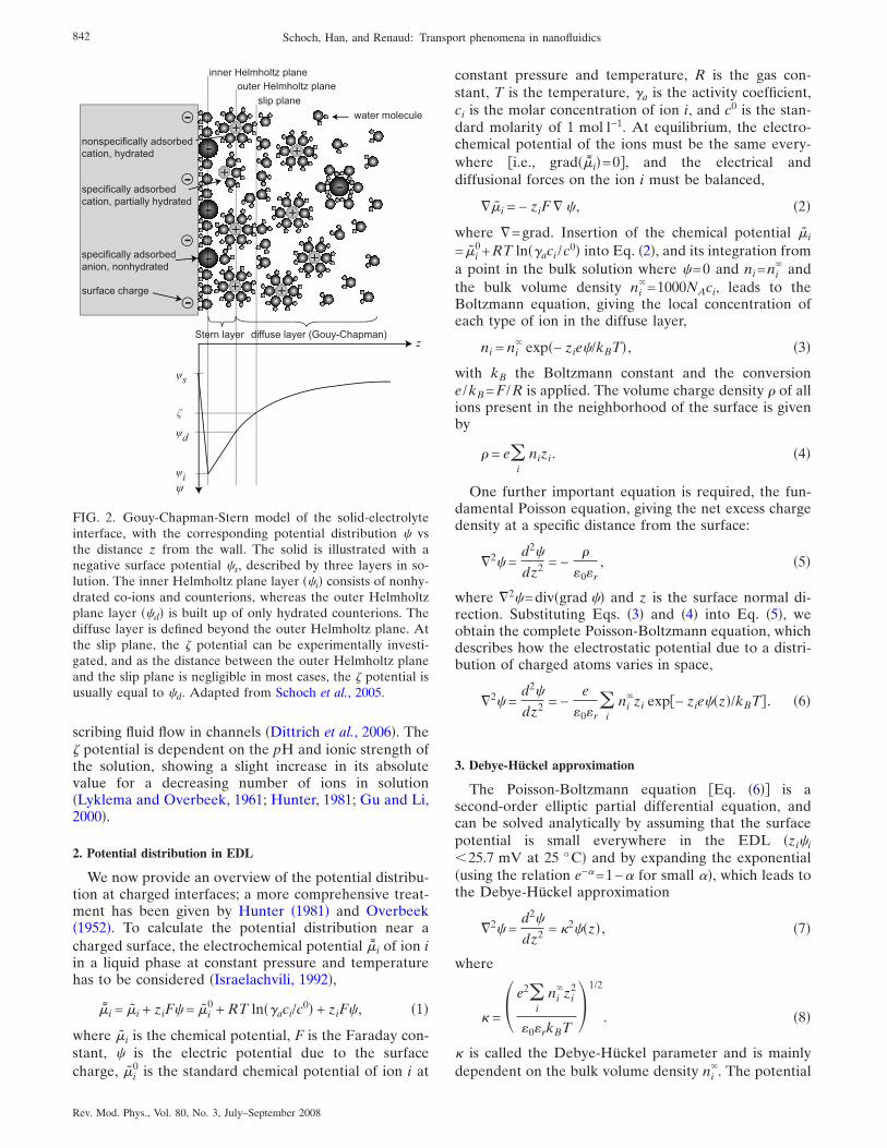
The electrical double layer was initially representedby a simple capacitor, usually attributed to the model ofHelmholtz. Gouy and Chapman treated one layer ofcharge smeared uniformly over a planar surface im-mersed in an electrolyte solution �Overbeek, 1952�.Stern recognized that the assumptions that the electro-lyte ions could be regarded as point charges and thesolvent could be treated as a structureless dielectric ofconstant permittivity were quite unsatisfactory. He intro-duced the Stern layer between the inner and outerHelmholtz planes, in which the charge and potential dis-tribution are assumed to be linear, and a diffuse layerfurther from the wall where the Gouy-Chapman theoryis applied. This model is presented in Fig. 2, which isseparated into three layers �Hunter, 1981�. The first layeris at the inner Helmholtz plane and bears the potential�i, where co-ions and counterions are not hydrated andare specifically adsorbed to the surface. The secondlayer is defined by the outer Helmholtz plane with po-tential �d, consisting of a layer of bound, hydrated, andpartially hydrated counterions. The outermost and thirdlayer is the diffuse layer, composed of mobile co-ionsand counterions, in which resides the slip plane bearingthe � potential �described hereafter�. In most cases, theouter Helmholtz plane and the slip plane are situatedclose to each other �Bhatt et al., 2005�, allowing the ap-proximation of �d with the � potential for practical pur-poses.
The slip plane, or shear surface, is an imaginary planeseparating ions that are immobile at the surface fromthose that are mobile in solution. The � potential at thisplane can be experimentally determined, and is there-fore an important parameter in colloid science for deter-mining the stability of particles, and in �TAS for de-
841Schoch, Han, and Renaud: Transport phenomena in nanofluidics
Rev. Mod. Phys., Vol. 80, No. 3, July–September 2008
scribing fluid flow in channels �Dittrich et al., 2006�. The� potential is dependent on the pH and ionic strength ofthe solution, showing a slight increase in its absolutevalue for a decreasing number of ions in solution�Lyklema and Overbeek, 1961; Hunter, 1981; Gu and Li,2000�.
2. Potential distribution in EDL
We now provide an overview of the potential distribu-tion at charged interfaces; a more comprehensive treat-ment has been given by Hunter �1981� and Overbeek�1952�. To calculate the potential distribution near acharged surface, the electrochemical potential �5 i of ion iin a liquid phase at constant pressure and temperaturehas to be considered �Israelachvili, 1992�,
�5 i = �̃i + ziF� = �̃i0 + RT ln��aci/c
0� + ziF� , �1�
where �̃i is the chemical potential, F is the Faraday con-stant, � is the electric potential due to the surfacecharge, �̃i
0 is the standard chemical potential of ion i at
constant pressure and temperature, R is the gas con-stant, T is the temperature, �a is the activity coefficient,ci is the molar concentration of ion i, and c0 is the stan-dard molarity of 1 mol l−1. At equilibrium, the electro-chemical potential of the ions must be the same every-where �i.e., grad��5 i�=0�, and the electrical anddiffusional forces on the ion i must be balanced,
��̃i = − ziF � � , �2�
where �=grad. Insertion of the chemical potential �̃i
= �̃i0+RT ln��aci /c0� into Eq. �2�, and its integration from
a point in the bulk solution where �=0 and ni=ni� and
the bulk volume density ni�=1000NAci, leads to the
Boltzmann equation, giving the local concentration ofeach type of ion in the diffuse layer,
ni = ni� exp�− zie�/kBT� , �3�
with kB the Boltzmann constant and the conversione /kB=F /R is applied. The volume charge density � of allions present in the neighborhood of the surface is givenby
� = e�i
nizi. �4�
One further important equation is required, the fun-damental Poisson equation, giving the net excess chargedensity at a specific distance from the surface:
�2� =d2�
dz2 = −�
0r, �5�
where �2�=div�grad �� and z is the surface normal di-rection. Substituting Eqs. �3� and �4� into Eq. �5�, weobtain the complete Poisson-Boltzmann equation, whichdescribes how the electrostatic potential due to a distri-bution of charged atoms varies in space,
�2� =d2�
dz2 = −e
0r�
ini�zi exp�− zie��z�/kBT� . �6�
3. Debye-Hückel approximation
The Poisson-Boltzmann equation �Eq. �6�� is asecond-order elliptic partial differential equation, andcan be solved analytically by assuming that the surfacepotential is small everywhere in the EDL �zi�i25.7 mV at 25 °C� and by expanding the exponential�using the relation e−�=1−� for small ��, which leads tothe Debye-Hückel approximation
�2� =d2�
dz2 = �2��z� , �7�
where
� = � e2�i
ni�zi
2
0rkBT�1/2
. �8�
� is called the Debye-Hückel parameter and is mainlydependent on the bulk volume density ni
�. The potential
-
-
-
-
-
-
-
-
inner Helmholtz planeouter Helmholtz plane
slip plane
ψs
ψi
ψd
ζ
ψ
z
specifically adsorbedanion, nonhydrated
nonspecifically adsorbedcation, hydrated
water molecule
specifically adsorbedcation, partially hydrated
surface charge
Stern layer diffuse layer (Gouy-Chapman)
+
+
+
+ +
+
++
FIG. 2. Gouy-Chapman-Stern model of the solid-electrolyteinterface, with the corresponding potential distribution � vsthe distance z from the wall. The solid is illustrated with anegative surface potential �s, described by three layers in so-lution. The inner Helmholtz plane layer ��i� consists of nonhy-drated co-ions and counterions, whereas the outer Helmholtzplane layer ��d� is built up of only hydrated counterions. Thediffuse layer is defined beyond the outer Helmholtz plane. Atthe slip plane, the � potential can be experimentally investi-gated, and as the distance between the outer Helmholtz planeand the slip plane is negligible in most cases, the � potential isusually equal to �d. Adapted from Schoch et al., 2005.
842 Schoch, Han, and Renaud: Transport phenomena in nanofluidics
Rev. Mod. Phys., Vol. 80, No. 3, July–September 2008

decays exponentially in the diffuse layer with the char-acteristic distance given by the Debye length D=�−1.This value corresponds to the thickness of the EDL,which increases with dilution as presented in Table I.For a symmetrical zi :zi electrolyte with concentration ciat 25 °C, the value of the Debye length D �unit ismeters� can be written as
D =3.04� 10−10
zici
=2.15� 10−10
Is
, �9�
where the ionic strength Is is
Is =12 � cizi
2. �10�
Consider that the region of varying potential extendsto a distance of about 3 D before the potential has de-cayed to about 2% of its value at the surface. Based onthe approximation zi�s25.7 mV, the solution of theDebye-Hückel approximation is
��z� = �s exp�− �z� . �11�
4. Gouy-Chapman model
As the Debye-Hückel approximation is not valid forhigh surface potentials, the Poisson-Boltzmann equationhas to be solved explicitly. Analytically, this can be doneonly under the assumption of a symmetrical electrolytewhere the valence of the co-ion is equal to the valence ofthe counterion, leading to the Gouy-Chapman equation
tanh�zi�̃�z�/4� = tanh�zi�̃s/4�exp�− �z� , �12�
where �̃=e� /kBT is the dimensionless potential, and at
25 °C �̃=1 for �=25.7 mV. For small values of �,tanh �� is valid �Taylor expansion�, and Eq. �12� re-duces to Eq. �11�. The Poisson-Boltzmann equation forhigh surface potentials and unsymmetrical electrolytescan only be solved numerically.
The resulting ion distribution from the Gouy-Chapman model is presented in Fig. 3�a�, where almostall the charge is balanced by the accumulation of coun-terions and relatively little by the reduction of co-ions.This is why it is possible to treat an unsymmetrical elec-trolyte system as symmetric, as is done in the Gouy-Chapman model, without incurring too much error.
When the Debye-Hückel approximation is used instead,the two ion types are of equal significance, as shown inFig. 3�b�.
5. Surface charge density
The surface charge density must balance the chargedensity in the adjacent solution,
�s = − �0
�
� dz . �13�
On substituting Eq. �5� and the integrated Eq. �6� intoEq. �13�, we obtain a relationship between the surfacecharge density �s and the surface potential �s,
�s = 0r�0
� d2�
dz2 dz
= �20rkBT�i
ni��exp�− zie�s/kBT� − 1��1/2
dz .
�14�
Since the surface potential �s is difficult to determineexperimentally, the charge density of the diffuse layercan be calculated by stopping the integration at theshear plane. We thus achieve an equation that relatesthe � potential to the diffuse layer charge density,
�d = �20rkBT�i
ni��exp�− zie�/kBT� − 1��1/2
dz ,
�15�
which has been used, for example, in a site-bindingmodel of the oxide-electrolyte interface �Yates et al.,1974�, and has shown consistency with experimentaldata obtained for oxides by potentiometric titrationmeasurements �Abendrot, 1970�.
TABLE I. EDL thicknesses D for typical KCl concentrationsat 25 °C.
KCl concentration �M� Debye length D �nm�
100 0.310−1 1.010−2 3.110−3 9.610−4 30.510−5 96.3 0 1 2 3 4
n-
n+
n+0=n-0
0 1 2 3 4
n-
n+
κ zκ z
(a) (b)
FIG. 3. Volume densities n+ and n− of positive and negativeions, respectively, near a negatively charged surface as a func-tion of the dimensionless number �z. Distribution from �a� theGouy-Chapman model, which shows an excess of positivelycharged ions, and �b� the Debye-Hückel approximation with asymmetrical co-ion and counterion distribution. Adapted fromHunter, 1981.
843Schoch, Han, and Renaud: Transport phenomena in nanofluidics
Rev. Mod. Phys., Vol. 80, No. 3, July–September 2008
6. Surface conductance
The EDL contains more ions than the bulk, whichresults in a surface conductance due to their motion inthe electric field �Urban et al., 1934; Kittaka andMorimoto, 1976�, and this conductance can be measuredin an ac field at sufficiently high frequency. Such conduc-tance measurements can also be performed in a dc field,but the electro-osmotic contributions �see Sec. II.B.1�must be considered. The measured surface conductanceGms in glass capillaries is given by
Gms = K�2�r0
d, �16�
where r0 is the radius of the capillary, d is its length, andK� is the normalized surface conductance, often referredto as the surface conductance in the literature. Decadesago, only the diffuse part of the EDL was considered forthe surface conductance K�, and values on the order of10−9–10−8 S were reported �Overbeek, 1952�.
However, for nonpenetrable surfaces, Lyklema andMinor �1998� showed that surface conductance does nottake place only in the diffuse part of the EDL; a signifi-cant amount occurs behind the slip plane, as has beenconfirmed by their experimental case study of sulfatedpolystyrene latex plugs. Therefore, they described thetotal conductance K� as the sum of the surface conduc-tance contributions from the diffuse part K�d and innerpart K�i of the EDL �Lyklema, 1995�,
K� = K�d + K�i. �17�
Lyklema et al. �1998� compared the EDL with a two-dimensional gel corresponding to the Stern layer. In thisgel, ions can move laterally almost unimpeded, and it isseparated from the mobile part of the fluid by the slipplane. For oxides, this hydrodynamically stagnant layercontains up to 85% of the counterions and thereforecontributes significantly to the overall conductance K�.Furthermore, the counterion mobility in this stagnantlayer is important in silica, for example, with 96% of thebulk mobility �Lyklema, 2001�. In order to relate thesurface conductance to the bulk conductivity KL,Lyklema and Minor �1998� have introduced the Dukhinnumber,
Du = K�/apKL, �18�
where ap is the radius of the particle in solution. If Du�1, the conductance mainly occurs along the chargedsurface of the particle. Lobbus et al. �2000� have re-ported that the contribution of the stagnant layer K�i tothe total surface conductance K� cannot be neglected,and that the Dukhin number increases with dilution.
7. Continuum models and molecular-dynamicssimulations
In this review, we focus on nanochannels with heightsbetween a few nanometers and 100 nm, a scale at whichcontinuum and mean-field theories are valid. However,these theories break down in smaller openings because
of the collisions between molecules and walls, and theimpurities and graininess of the substrate �Fulinski et al.,2004�.
At such length scales, molecular-dynamics simulationsare used to determine transport in nanopores for a spe-cific period of time with known physical laws �Qiao andAluru, 2003, 2005; Lu et al., 2004�. In a typicalmolecular-dynamics simulation, a set of molecules withinitial random positions is assumed, to which are as-signed initial random velocities corresponding to theBoltzmann distribution at the temperature of interest.The time evolution of the atomic positions is obtainedby numerically integrating Newton’s law of motion forsingle atoms.
It is important to consider that the applicability of theGouy-Chapman model and the Poisson-Boltzmannequation are limited by the finite size of the componentions and the effect of these ions on the relative permit-tivity of the solvent, because of which stochastic, nonde-terministic Monte Carlo simulations have been applied�Yang and Yiacoumi, 2002; Fawcett and Smagala, 2006�.
It can be difficult to obtain the continuum limit frompreviously described simulations because simulated sys-tems are usually limited to tens of nanometers and timescales of nanoseconds. This restraint can be overcomewith sufficiently coarse-grained simulation techniquessuch as dissipative particle dynamics �Groot and Warren,1997� to reveal the physics of nanopores and nanochan-nels �Duong-Hong et al., 2007�. In order to reduce com-puting time, the density-functional theory has been ap-plied to nanochannels, demonstrating good agreementcompared to Monte Carlo and molecular-dynamicssimulations �Nilson and Griffiths, 2006�.
B. Electrokinetic effects in nanochannels
Fluid flow in nanochannels is conveniently achievedby electrokinetic techniques or capillary forces. Thenonmechanical manipulation of fluid by electrokineticeffects is commonly used and is presented subsequently,whereas capillary forces have been described in the re-view of microfluidics by Squires and Quake �2005�,which we briefly complement with nanofluidic studies.
In nanochannels, capillary pressures up to −17 barshave been reported �Tas et al., 2003�, allowing for thespontaneous filling of such channels with liquid. The po-sition of the moving meniscus in nanochannels as a func-tion of time has been modeled �Washburn, 1921; Tas etal., 2004�, but after a certain filling length, the formationof bubbles by the enclosure of air is typically encoun-tered, a problem that has been addressed �Han, Mondin,Hegelbach, et al., 2006; Riehn and Austin, 2006�. Forcapillary filling studies, the behavior of liquid in shallownanochannels down to 6 nm can be monitored with aFabry-Perot interferometer by measuring the refractiveindex of the medium inside the channel �Delft et al.,2007�.
Pressure-driven flow can also be used in nanochan-nels, but high pressures �Tegenfeldt, Prinz, and Cao,2004� are needed to obtain fluid flow because the pres-
844 Schoch, Han, and Renaud: Transport phenomena in nanofluidics
Rev. Mod. Phys., Vol. 80, No. 3, July–September 2008

sure has a power-law relation with the height of thechannel �Squires and Quake, 2005�. In microchannels,fluid manipulation with hydrostatic pressure is oftenused, but the achievement of well-controlled fluid flow ischallenging �Futterer et al., 2004; Johann and Renaud,2004; Eijkel and van den Berg, 2005b�.
1. Basic physics of electrokinetics
The motion of electrically charged molecules and par-ticles due to an applied electric field in moving sub-stances such as water is studied in electrokinetics. Thisfield covers electro-osmosis, electrophoresis, dielectro-phoresis, and electrorotation; here we emphasize thefirst two processes and subsequently present their basicphysics.
�a� Electro-osmosis. If a charged surface is in contactwith a liquid and an electric field is applied parallel tothe interface, movement of liquid adjacent to the walloccurs. If the surface is negatively charged, the net ex-cess of positive ions in the EDL will draw the liquidalong because of viscous interactions, which results inflow toward the cathode �Schmid, 1998�. At the slipplane, the liquid velocity is zero and increases to a maxi-mum value with the electro-osmotic velocity veo at somedistance from the wall, after which it remains constant athigh ionic strength of the solution in a nanochannel.This plug flow was first described by Smoluchowski�1916, 1918�,
veo = −0r�Ex
�, �19�
where Ex is the electric field in the x direction and � isthe dynamic �shear� viscosity of the fluid. The electro-osmotic mobility is �eo=0r� /�. The � potential can bechanged by active control of electro-osmotic flow usinglight �Moorthy et al., 2001�, the inversion of electro-osmotic flow with surface coatings by polyelectrolytes�Wu et al., 2001; Sui and Schlenoff, 2003; Adamczyk etal., 2004�, or the difference in the electro-osmotic flow intwo different composite microchannels �Bianchi et al.,2001�.
If the EDL can develop fully in the nanochannel, theelectric potential reduces to zero in the center. However,if the ionic strength is low, the EDLs will overlap in thenanochannel and affect electro-osmosis, which is nolonger plug flow but instead follows the electric poten-tial ��z� �Fig. 4�. This phenomenon was first investigatedby Burgreen and Nakache �1964�, Levine, Marriott, andRobinson �1975�, and complemented by Levine, Marri-ott, Neale, et al. �1975� in capillary slits, whereas Riceand Whitehead �1965� described flow in cylindrical cap-illaries. Under low ionic strength conditions, the electro-osmotic velocity veo is dependent on the potential distri-bution ��z� between two parallel plates �discussed belowin Eq. �52�� and is given by
veo = −0r�Ex
��1 −
��z��
� . �20�
�b� Electrophoresis. Electrophoresis is a common
technique used to move ions and molecules in microflu-idic and nanofluidic channels �Oddy and Santiago, 2004�.A simplified definition is that electrophoresis is the con-verse of electro-osmosis; the liquid is regarded as fixed,so that a molecule moves in the opposite direction rela-tive to the solution. The complete description of electro-phoresis has been given by Morgan and Green �2003�,and is summarized here.
When a molecule is placed in an aqueous medium, theEDL screens the charges of the molecule, so that overallit is electroneutral and appears to have a zero netcharge. Placing the molecule in an electric field results inits movement because ions in the EDL are not fixed tothe surface. The counterions in the EDL are mobile andmove in the direction opposite to that in which the mol-ecule would move if it were unscreened. This ion move-ment gives rise to fluid motion around the molecule�electro-osmosis�, and because of the viscosity of theaqueous medium, the fluid is stationary on a globalscale. This results in ion movement as the molecule ispushed backward in the opposite direction.
Therefore, the electrophoretic mobility is dependenton the thickness of the electrical double layer and can bedivided into categories of thin and thick EDLs, de-scribed by the product �ap of the Debye-Hückel param-eter � and the molecular radius ap.
Thin electrical double layer, �ap�1. For an EDL thatis thin compared to the molecular radius, electrophore-sis is the converse of electro-osmosis �Eq. �19��. In thiscase, however, the surface moves relative to the station-ary fluid, and the electrophoretic mobility is given by theHelmholtz-Smoluchowski limit,
�ep =0r�
�. �21�
Thick electrical double layer, �ap�1. When a mol-ecule has a thick EDL, the force acting on the moleculeis the difference between the drag and Coulomb forces.The drag force is given by Stokes law qEx= fvep, leadingto �ep=vep/Ex=q / f=q /6��ap, where f is the friction co-efficient and vep is the electrophoretic velocity. The �
z = 0 z = h
Ψ(z)
Ψ = 0
Ψ = ζ
FIG. 4. Schematic representation of the potential distributionin a nanochannel with height h in direction z when the EDLsoverlap �solid line�, compared to the EDL potentials if theopposite wall is not present �dashed line�. Adapted fromSchoch, 2006.
845Schoch, Han, and Renaud: Transport phenomena in nanofluidics
Rev. Mod. Phys., Vol. 80, No. 3, July–September 2008
potential can be identified with the potential of a pointcharge as �=apE=apq /4�0r. The combination of theseexpressions leads to the electrophoretic mobility in theHückel-Onsager limit,
�ep =20r�
3�. �22�
The real situation is more complex than that de-scribed above, as co-ions around the molecule moveahead and counterions move in the direction opposite tothe molecule. This results in a polarization field, whichcan increase or decrease the electrophoretic mobility. Asecond issue, which has not been considered, is the dis-tortion of the field induced by movement of the mol-ecule, known as the relaxation effect.
�c� Streaming potential. When a liquid is forced to flowthrough a small channel under hydrostatic pressure, ionsin the mobile part of the EDL are carried downstream.This creates an electric current, which is called thestreaming current, flowing in the same direction as theliquid. The accumulation of ions downstream sets up anelectric field, which causes a current to flow in the oppo-site direction through the liquid �conduction current�.When the conduction current is equal to the streamingcurrent, steady state is achieved. The resultant electro-static potential difference between the two ends of thechannel is referred to as the streaming potential �.
These properties are exploited to determine the � sur-face potential, which is done by either measuring thestreaming potential �Horn and Onoda, 1978; Mockel etal., 1998; Gu and Li, 2000� or measuring the streamingcurrent directly �Jednacak and Pravdic, 1974�. Thestreaming potential can also be measured with a nano-scale probe over the changes in the counterion concen-tration of the EDL. This concentration is dependent onthe flow speed, and therefore results in a conductancechange of the nanoprobe located in the EDL �Bourlon etal., 2007�. In the case of EDL overlap in nanochannels, acorrection factor for the streaming potential has to beconsidered �Burgreen and Nakache, 1964�, and it hasbeen reported that under such conditions the streamingpotential has a constant value due to length-scale effects�Shim et al., 2007�.
�d� Electroviscous effect. Whenever an electricaldouble layer at an interface in an ionic liquid is sheared,a potential difference in the form of a streaming poten-tial is established, which will tend to resist the flow ofliquid �Elton, 1948�. This potential will produce a back-flow by electro-osmosis, and the net effect is a dimin-ished flow in the forward direction. The liquid appearsto exhibit enhanced viscosity if its flow rate is comparedto the flow without EDL effects. This phenomenon isdenoted the electroviscous effect and is classified as fol-lows �Hunter, 1981�.
The primary electroviscous effect occurs in channelssufficiently large to allow complete development of theEDL and can be measured in microchannels �Ren et al.,2001; Vainshtein and Gutfinger, 2002�.
The secondary electroviscous effect refers to an in-crease in the apparent viscosity of a fluid as a result ofEDL interactions �Yang and Li, 1997�. Tas et al. �2004�have observed that the capillary filling speed of deminer-alized water in 53-nm-high nanochannels is lower thanexpected from capillary action. This is attributed to thesecondary electroviscous effect, and the apparent viscos-ity has been measured as being 24% higher than thebulk viscosity.
A real increase in the viscosity due to high electricfields in the neighborhood of a surface, for example, isreferred to as the viscoelectric effect.
2. Comprehensive electrokinetic theory for nanochannels
It is important to consider aforementioned electroki-netic phenomena to develop a comprehensive transportmodel of molecules in nanochannels. Such processeshave been described in the field of membrane science. Innanofiltration, the Teorell-Meyer-Sievers model can beapplied; it assumes a uniform distribution of fixedcharge, mobile ions, and electric potential �Hagmeyerand Gimbel, 1999; Bowen and Welfoot, 2002; Garcia-Aleman and Dickson, 2004�. However, these assump-tions are not applicable to membranes with pores con-taining a radius bigger than the Debye length, leading tothe proposition of the space-charge model by Gross andOsterle �1968�, and its development by Wang et al.�1995�. The validity of this model to describe the elec-trokinetic phenomena in charged capillaries and trans-port through porous membranes has been confirmed�Szymczyk et al., 1999; Yaroshchuk et al., 2005�. Thespace-charge model is an extension of the Teorell-Meyer-Sievers model and is more calculation intensive,mathematically complicated, and computationally ex-pensive, which makes it difficult to apply to solutions ofmixed electrolytes. This led to the development of sim-plified approaches for modeling ion transport throughporous membranes �Hawkins Cwirko and Carbonell,1989; Smit, 1989; Basu and Sharma, 1997�.
The space-charge model is one of the most completephysical interpretations of ion transport throughnanometer-sized channels, which are assumed to bestraight and bear a surface charge. The following equa-tions are solved: �1� the Poisson equation for the distri-bution of the electric potential in nanochannels, �2� theNernst-Planck equation for ion transport, and �3� theNavier-Stokes equations for laminar volumetric fluidflow. The Poisson and Nernst-Planck equations give iondistributions “beyond” the Poisson-Boltzmann �Eq. �6��because they allow flows and other forces to drive ionfluxes. In the absence of other flows and forces, the Pois-son and Nernst-Planck equations give the Poisson-Boltzmann equation.
�a� Poisson equation and Boltzmann distribution. Theelectric potential is divided into two parts,
� = ��x,z� + ��x� , �23�
where � originates from the surface charge of thenanochannel and � is due to the streaming potential,
846 Schoch, Han, and Renaud: Transport phenomena in nanofluidics
Rev. Mod. Phys., Vol. 80, No. 3, July–September 2008

with x the longitudinal direction and z the direction nor-mal to the nanochannel surface. To calculate the electricpotential in nanochannels, the following assumptionscan be made since the nanochannels are much longerthan they are high �Sasidhar and Ruckenstein, 1982�. �1�The variations of the potential in x are much smallerthan in the z direction. �2� The concentration variationin the z direction at any x position follows the equilib-rium Boltzmann distribution, because normal ionic cur-rents have to be compensated due to diffusion and elec-tromigration within the EDL �Dukhin and Shilov, 1969�,
c± = z�c* exp��z±e�/kBT� , �24�
where c* is the bulk concentration at negligible electro-static interactions. With these two assumptions, the elec-tric potential in nanochannels is given by the Poissonequation,
�2� = −F
0r�i=1
2
zici, �25�
where i=1 indicates the cations and i=2 the anions.�b� Nernst-Planck equation. The second equation is
the extended Nernst-Planck equation, which accountsfor the transport of charged molecules in the presence ofan electric potential through the nanochannel. The totalflux per area Ji of ion i includes contributions from dif-fusional flux, migration of molecules in the electric field,and convective flux in the nanochannel,
Ji = − Di � ci −ziF
RTDici � � ± vcci, �26�
where Di is the diffusion coefficient of ion i and vc is theconvective velocity field. The extended Nernst-Planckequation includes the contribution of convective flux,unlike the ordinary Nernst-Planck equation. Equation�26� is the sum of three terms, as follows:
• Fick’s first law, which specifies the diffusion of mol-ecules due to a chemical potential gradient �concen-tration gradient�.
• The flux due to the electric potential �.
• Convective transport, which can be due to pressure,mechanical stirring, and external fields such as elec-tric and magnetic fields �Fair and Osterle, 1970; vander Horst et al., 1995; Bowen et al., 1997; Garba et al.,1999�. In nanopores, electro-osmotic transport due toan electric field has to be considered �Kemery et al.,1998; Bath et al., 2000; Bhattacharjee et al., 2001;Miller et al., 2001; Gasparac et al., 2003�. The direc-tion of vc is dependent on the surface charge of thenanochannel, and is in the opposite direction fromthe first two contributions if the surface charge isnegative.
�c� Navier-Stokes equations. The third contribution tothe space-charge model is the Navier-Stokes equations,which represent a conservation of momentum in a dif-ferential form and are used to calculate vc. For incom-pressible Newtonian fluids, in which the viscosity is not
dependent on shear stress �Gross and Osterle, 1968;Marshall and Mocskos, 1997�, by neglecting inertia�Sasidhar and Ruckenstein, 1982�, and assuming con-stant viscosity in the Navier-Stokes equations, the move-ment of fluid through channels is given by
�vc = 0, �27�
− �p − Fb�i=1
2
zici � � − Fb�i=1
2
zici � � + ��2vc = 0, �28�
where Eq. �27� is the continuity equation, p is the exter-nal pressure, and Fb is the body force. Equation �28�contains three different forces acting on any volume el-ement inside the channel: �1� a mechanical force due tothe internally generated pressure gradient �the firstterm�, �2� a body force that develops because of the po-larization of the EDL �caused by the concentration gra-dient through the nanochannel, the second term�, and�3� a second body force caused by the streaming poten-tial �the flow component due to the latter force is theelectro-osmotic flow, the third term�. All these forces�1�–�3� balance the viscous force generated by the con-vective motion of fluid �the fourth term in Eq. �28��.
The Navier-Stokes equations are usually solved withthe assumption of zero relative fluid-solid velocity, calledthe no-slip boundary condition. However, observed flowrates in nanotubes exceeded values calculated from con-ventional hydrodynamics by more than three orders ofmagnitude �Majumder et al., 2005; Holt et al., 2006�,demonstrating nearly frictionless flow. Parameters af-fecting such fluid slip are an interplay of surface rough-ness, dissolved gas, pressure, wetting, shear rate, andelectrical properties �Neto et al., 2005; Squires andQuake, 2005; Lauga et al., 2006; Seth et al., 2007�. Webelieve that further knowledge of liquid slip is importantfor nanofluidics because of the potential to design sys-tems with enhanced fluid transport �Cheng and Gior-dano, 2002; Eijkel, 2007�.
�d� Application to nanochannels. The space-chargemodel has been simplified by Pennathur and Santiago�2005a� to describe electrokinetic transport in longnanochannels, confirmed by their experimental studies�Pennathur and Santiago, 2005b�. Assuming fully devel-oped flow and negligible contributions from pressuregradients, they obtained the following expression forelectrokinetic flow in nanochannels:
veo + vep =0r�Ex
�W�exp�− zie���z� − �s�
kBT�
��1 −��z��
� + zi�epEx, �29�
where W= �exp�−zie��z� /kBT�� and � � represents thecross-sectional averaged quantity. The exponential termin Eq. �29� describes the transverse distribution of thesample determined by analyte valence zi, and the trans-verse potential distribution ��z�. The product of this ex-ponential with 1−��z� /� captures the coupling between
847Schoch, Han, and Renaud: Transport phenomena in nanofluidics
Rev. Mod. Phys., Vol. 80, No. 3, July–September 2008
transverse electromigration and diffusion with stream-wise flow.
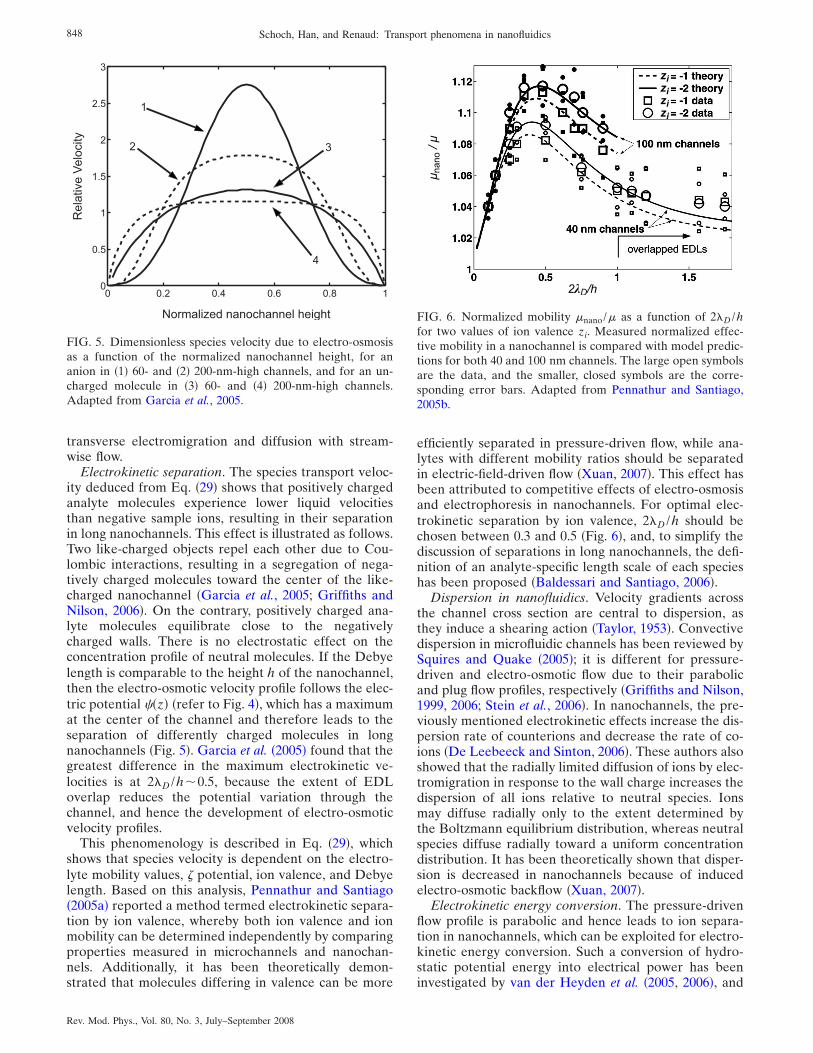
Electrokinetic separation. The species transport veloc-ity deduced from Eq. �29� shows that positively chargedanalyte molecules experience lower liquid velocitiesthan negative sample ions, resulting in their separationin long nanochannels. This effect is illustrated as follows.Two like-charged objects repel each other due to Cou-lombic interactions, resulting in a segregation of nega-tively charged molecules toward the center of the like-charged nanochannel �Garcia et al., 2005; Griffiths andNilson, 2006�. On the contrary, positively charged ana-lyte molecules equilibrate close to the negativelycharged walls. There is no electrostatic effect on theconcentration profile of neutral molecules. If the Debyelength is comparable to the height h of the nanochannel,then the electro-osmotic velocity profile follows the elec-tric potential ��z� �refer to Fig. 4�, which has a maximumat the center of the channel and therefore leads to theseparation of differently charged molecules in longnanochannels �Fig. 5�. Garcia et al. �2005� found that thegreatest difference in the maximum electrokinetic ve-locities is at 2 D /h�0.5, because the extent of EDLoverlap reduces the potential variation through thechannel, and hence the development of electro-osmoticvelocity profiles.
This phenomenology is described in Eq. �29�, whichshows that species velocity is dependent on the electro-lyte mobility values, � potential, ion valence, and Debyelength. Based on this analysis, Pennathur and Santiago�2005a� reported a method termed electrokinetic separa-tion by ion valence, whereby both ion valence and ionmobility can be determined independently by comparingproperties measured in microchannels and nanochan-nels. Additionally, it has been theoretically demon-strated that molecules differing in valence can be more
efficiently separated in pressure-driven flow, while ana-lytes with different mobility ratios should be separatedin electric-field-driven flow �Xuan, 2007�. This effect hasbeen attributed to competitive effects of electro-osmosisand electrophoresis in nanochannels. For optimal elec-trokinetic separation by ion valence, 2 D /h should bechosen between 0.3 and 0.5 �Fig. 6�, and, to simplify thediscussion of separations in long nanochannels, the defi-nition of an analyte-specific length scale of each specieshas been proposed �Baldessari and Santiago, 2006�.
Dispersion in nanofluidics. Velocity gradients acrossthe channel cross section are central to dispersion, asthey induce a shearing action �Taylor, 1953�. Convectivedispersion in microfluidic channels has been reviewed bySquires and Quake �2005�; it is different for pressure-driven and electro-osmotic flow due to their parabolicand plug flow profiles, respectively �Griffiths and Nilson,1999, 2006; Stein et al., 2006�. In nanochannels, the pre-viously mentioned electrokinetic effects increase the dis-persion rate of counterions and decrease the rate of co-ions �De Leebeeck and Sinton, 2006�. These authors alsoshowed that the radially limited diffusion of ions by elec-tromigration in response to the wall charge increases thedispersion of all ions relative to neutral species. Ionsmay diffuse radially only to the extent determined bythe Boltzmann equilibrium distribution, whereas neutralspecies diffuse radially toward a uniform concentrationdistribution. It has been theoretically shown that disper-sion is decreased in nanochannels because of inducedelectro-osmotic backflow �Xuan, 2007�.
Electrokinetic energy conversion. The pressure-drivenflow profile is parabolic and hence leads to ion separa-tion in nanochannels, which can be exploited for electro-kinetic energy conversion. Such a conversion of hydro-static potential energy into electrical power has beeninvestigated by van der Heyden et al. �2005, 2006�, and
RelativeVelocity
Normalized nanochannel height
0 0.2 0.4 0.6 0.8 10
0.5
1
1.5
2
2.5
3
1
2 3
4
FIG. 5. Dimensionless species velocity due to electro-osmosisas a function of the normalized nanochannel height, for ananion in �1� 60- and �2� 200-nm-high channels, and for an un-charged molecule in �3� 60- and �4� 200-nm-high channels.Adapted from Garcia et al., 2005.
2λD/h
μ nano/μ
zi
zizizizi
FIG. 6. Normalized mobility �nano/� as a function of 2 D /hfor two values of ion valence zi. Measured normalized effec-tive mobility in a nanochannel is compared with model predic-tions for both 40 and 100 nm channels. The large open symbolsare the data, and the smaller, closed symbols are the corre-sponding error bars. Adapted from Pennathur and Santiago,2005b.
848 Schoch, Han, and Renaud: Transport phenomena in nanofluidics
Rev. Mod. Phys., Vol. 80, No. 3, July–September 2008

this principle can be used for the development of microfuel cells �Liu et al., 2005� or electrokinetic pumps �Minet al., 2004�. The maximum energy conversion efficiencyis obtained for 2 D /h�1 �Morrison and Osterle, 1965;Daiguji, Yang, Szeri, et al., 2004� and has been measuredto be �3% �van der Heyden et al., 2007�, which is lowcompared to typical fuel cell efficiencies of 50%.
C. Electrode-electrolyte interface
As an introduction to Sec. III.A about the electricalcharacterization of nanofluidic systems, we now describehow the electrode-electrolyte interface can be modeledby an electric equivalent circuit �Kovacs, 1994�.
The interface between the electrode and the ionic so-lution can be represented by its capacitance CEDL, whichis the capacitance sum of the Helmholtz layer CH andthe Gouy-Chapman layer CGC,
1
CEDL=
1
CH+
1
CGC. �30�
The Helmholtz layer can be modeled as a simple ca-pacitance,
CH =0rA
dOHP, �31�
where dOHP is the distance from the electrode to theouter Helmholtz plane �see Fig. 2�. The capacitance ofthe Gouy-Chapman layer is obtained by differentiatingEq. �14�,
CGC =d�s
d�s=0r
Dcosh�zie�s
kBT� . �32�
1. Charge-transfer resistance
Modeling the electrode-electrolyte interface by ca-pacitance does not describe the entire electric circuit. Aresistive path must be considered in parallel to the ca-pacitive path because a current can flow across the inter-face when a dc potential is applied. In order to definethe resistive path in terms of the charge-transfer resis-tance Rt, we briefly discuss electrochemistry.
When a metal is placed in an electrolyte, chemicalreactions will occur at the interface, whereby electronsare transferred between the metal and the ionic solution.This results in the formation of an electric field at theelectrode surface, which affects further chemical reac-tions. Initially, the energy barrier for oxidation is lowerthan for reduction. As the reaction proceeds, excesselectrons in the metal accumulate until the potential in-creases, which reduces the barrier for the reverse reac-tion �Kovacs, 1994�. These two competing reactionseventually reach equilibrium, resulting in a zero net cur-rent across the interface. The absolute value of the cur-rent �per unit area� due to oxidation and reduction isreferred to as the exchange current density Id0
.Thus, there is a constant flow of charge across the
interface at equilibrium, but the net flow is zero. To
achieve a flow of current, a net movement of charge isrequired, which is obtained when a potential Va is ap-plied to push the total potential across the interface,away from its equilibrium value V0. This potential dif-ference Va−V0 leads to the total overpotential �to,which is principally made from the sum of two overpo-tentials originating in the charge-transfer processes ofthe EDL leading to the charge-transfer overpotential�ct, and the diffusion of reactants to and from the elec-trode. For operation of an electrode near its equilibriumcondition, the charge-transfer overpotential �ct domi-nates the overall current. As the potential moves furtherfrom equilibrium, the overpotential due to the diffusionof reactants may become a limiting factor.
The exchange current density Id0is dependent on the
material properties of the electrode, the electrolyte com-position, and reactions taking place on the electrode. Asthe electrochemical reaction that dominates the ex-change current is often unknown, the calculation of Id0
isdifficult and is therefore experimentally determined bymeasuring the charge-transfer resistance Rt around theequilibrium potential of the electrode in the electrolyte�see Eq. �33��. The exchange current density Id0
is thenused to calculate the electrical current density Id as afunction of the charge-transfer overpotential �ct, as de-scribed by the Butler-Volmer equation �Park and Yoo,2003�,
Id = Id0�exp� �1 − ��zie�ct
kBT� − exp�− �zie�ct
kBT�� , �33�
where � is the symmetry factor that reflects the energybarrier differences for oxidation and reduction reac-tions. To obtain an appreciable current density Id, notethat the exchange current density Id0
determines themagnitude of the charge-transfer overpotential �ct.Therefore, the appropriate choice of the electrode ma-terial affects the amount of current that flows in re-sponse to an applied potential. Since electrochemical re-actions and gas evolution at the interface often occur athigher voltages, it is desirable to limit excursions fromequilibrium as much as possible. Hence, electrode mate-rials with a high exchange current density �like plati-num� are desirable for integration into microfluidic andnanofluidic systems.
This leads to the definition of the charge-transfer re-sistance Rt that appears in parallel to the interfacial ca-pacitance, which under low-field conditions with �=0.5�nonrectifying system� in the linear regime is given by
Rt =kBT
zieId0
. �34�
In summary, the model of a metal electrode placed inan electrolyte can be represented by a capacitance CEDLin parallel to the charge-transfer resistance Rt. The rela-tive impedance of these two elements determines thebasic characteristics of the electrode. If the electrode hasa high exchange current density, the charge-transfer re-sistance tends toward zero �Id0
→� ,Rt→0�, as for
849Schoch, Han, and Renaud: Transport phenomena in nanofluidics
Rev. Mod. Phys., Vol. 80, No. 3, July–September 2008

Ag/AgCl electrodes. Even though a significant currentdensity flows across the interface, no substantial overpo-tential develops. This is referred to as an ideally nonpo-larizable interface, and describes the optimum materialin this case. The opposite situation �Id0
→0,Rt→� � re-sults in what is called an ideally polarizable interface. Itbehaves like a capacitance with no Faradaic processesoccurring.
The charge-transfer overpotential �ct has been pre-sented above; it is important for small applied potentialsVa. If the magnitude of this potential is increased, reac-tants are not able to diffuse from the bulk to the inter-face fast enough, and the current becomes diffusion lim-ited. This results in a diffusional impedance ZW in serieswith the charge-transfer resistance Rt, and ZW can berepresented by either a series or parallel combination ofresistance and capacitance. In 1899, Warburg proposed amodel for this diffusional impedance ZW, which is pro-portional to 1 over the square root of the frequency �De-Rosa and Beard, 1977; McAdams et al., 1995�.
2. Constant phase element
It is often experimentally observed �Metz, 2003;Gawad, 2004� that the impedance deviates from thepurely capacitive behavior, that is expected theoreticallyfor smooth and clean surfaces like that of liquid mer-cury. In such situations, the impedance spectrum ZCPE ismodeled by a constant phase element �CPE� �Mac-Donald, 1987�, showing a power-law frequency depen-dence,
ZCPE��� =1
CCPE�j��nCPE, �35�
where � is the frequency, CCPE is the CPE capacitance,nCPE is the CPE exponent, and j is the imaginary unit.For perfectly smooth and clean electrodes, nCPE is equalto unity, resulting in ideal capacitive behavior. However,if the electrode has a microscopic roughness due toscratches, pits, etc., the effective solution resistance var-ies along the surface, and the current density is inhomo-geneous on a microscopic scale. This results in a CPEexponent in the range of 0.5nCPE1.
The constant phase element obtained its name be-cause the phase angle of ZCPE is independent of the fre-quency, and has a value of −�90nCPE�. It is a nonintuitivecircuit element that was invented while looking at theresponse of whole systems �MacDonald, 1987�.
III. PHENOMENA AT THE MICROCHANNEL-NANOCHANNEL INTERFACE
In order to investigate a nanochannel, it must be con-nected to the macroscopic world, which consequentlyleads to an interface between a nanochannel and typi-cally a microchannel �see Sec. VI, Fig. 32�. Differenttechniques can be used to probe a nanometer-sizedopening, and we begin with a description of the electri-cal characterizations that reveal the unique properties ofthese channels. The electric field and fluid flow in a
nanochannel can be substantially different from those inthe connecting microchannel, resulting in large gradientsat the geometric interface. These effects have been de-scribed in membrane science, where a porous membraneis in contact with a bulk solution, from which the Don-nan potential is known and subsequently introduced.Then we present fluorescence measurements and mod-eling of the exclusion-enrichment effect in nanochannelsat the diffusional limit and with external driving forcesas electric fields and pressures. This phenomenon is gen-erally described by partitioning at the microchannel-nanochannel interface, which takes into account electro-static and steric contributions. Finally, we provide insightinto the complex process of concentration polarizationat ion-selective interfaces.
A. Electrical characterization of nanochannels
Electrical measurements of nanochannels are per-formed because they do not require fluorescent labelsand are integrable on a chip, which is favorable for po-tential applications. Furthermore, electrical character-izations of fluidic systems can readily be parallelized.
First, we focus on impedance spectroscopy to measurethe nanochannel conductance. It has been shown that asimple physical model for ion transport through ananochannel can explain its conductance value at vary-ing ionic strengths. Indeed, we see that a conductanceplateau �on a log-log scale� is obtained at low ionicstrength when the Debye length becomes comparable tothe characteristic dimension of the nanochannel. Thiseffect is explained by an excess of mobile counterions inthe nanometer-sized aperture, which equilibrate the sur-face charge to maintain electroneutrality. Subsequently,we demonstrate that ion flow can be regulated withchemical surface modifications and field-effect modula-tions.
A nanochannel can be distinguished from a nanoporeby its length, as the nanochannel length is much longerthan the nanometer characteristic dimension of theopening, whereas a nanopore has a length approxi-mately within an order of magnitude of its minimalopening dimension. We show that if a nanopore ornanochannel has an asymmetric geometry or surfacecharge distribution along its longitudinal axis, ionic cur-rent rectification is obtained, as in a diode.
1. Impedance spectroscopy
To electrically characterize nanochannels that are in-terfaced with microchannels, we recommend the place-ment of electrodes as close as possible to the nanochan-nel openings in order to increase the sensitivity �Schoch,2006�. Therefore, the electrodes have to be integratedinto the microchannels, which can be achieved with stan-dard microfabrication techniques. Platinum electrodeswere used by Schoch et al. �2005�, because this materialhas a low chemical reactivity and hence will not be re-duced or oxidized when electric potentials are applied.However, the platinum electrodes bear an overpotential,
850 Schoch, Han, and Renaud: Transport phenomena in nanofluidics
Rev. Mod. Phys., Vol. 80, No. 3, July–September 2008

and when an electric potential is applied, this results in astart-up current peak and a decay with the square rootof time, as described by chronoamperometry and theCottrell equation �Girault, 2004�,
I�t� = nFAcRDR
�t, �36�
where n is the number of electrons transferred per mol-ecule, A is the electrode surface, cR is the concentrationof the reduced species R, and DR is the diffusion coeffi-cient of the reduced species R. Equation �36� describesthe fact that the current I induces oxidation and reduc-tion at the electrodes, and therefore the formation of thegases O2 and H2. After a few seconds, this results in adiffusion-limited current because generation of hydro-gen and oxygen can only occur at the same rate as thediffusion of the deposition products into solution. Natu-ral convection prevents the current from dropping tozero in reality, leading to drifting currents.
These problems can be overcome by performing acinstead of dc measurements. When the current flowchanges its direction each half-cycle of the sinusoidalapplied voltage, the system can be regarded as sym-metrical. Diffusion-limited currents cannot occur andchemical reactions are not induced because of the alter-nating electric field �Asbury and Engh, 1998�.
The electrical properties of materials and their inter-faces with electrodes can be characterized with imped-ance spectroscopy �MacDonald, 1987�. This method canbe used to investigate the dynamics of bound or mobilecharges in the bulk or interfacial regions of any kind ofsolid or liquid material. Impedance spectroscopy in-volves relatively simple electrical measurements that canreadily be automated, the results of which may often becorrelated with many complex material variables. Gen-erally, the most common and standard approach is tomeasure the impedance directly in the frequency do-main by applying a single-frequency voltage to the inter-face and measuring the phase shift and amplitude, orreal and imaginary parts, of the resulting current at thatfrequency.
Impedance spectroscopy has only recently been usedto describe nanometer-characteristic openings. Yi et al.�2005� demonstrated the detection of DNA molecules ina nanogap due to permittivity changes, and Ionescu-Zanetti et al. �2006� analyzed sensitivity to sample per-mittivity changes. They reported the detection limit ofthe impedance to be a 1.7% change in permittivity,showing the promise of nanogaps for label-free biomol-ecule detection on platforms amenable to high-throughput configurations. The impedance imaging ofindividual pores in a porous membrane has been dem-onstrated by Ervin et al. �2005, 2006� using a low-impedance bypass channel around the membrane toshunt the ion current. Cannon et al. �2003� analyzed theresistances of individual fluidic elements on their device,which consisted of two microchannels connected via ananoporous membrane in a multilayer microfluidic ar-chitecture. Polymer electrolytes confined to a porous
polycarbonate membrane were exposed by Layson andTeeters �2004� to different temperature and humidityconditions, and impedance spectroscopy measurementsallowed deeper insight into the changes of the polyelec-trolytes. Terrettaz et al. �2003� used impedance spectros-copy on planar gold substrates to monitor ion-channelprotein activity modulations by the selective binding ofan antibody.
Schoch �2006� performed impedance spectroscopymeasurements of nanochannels interfaced by two micro-channels containing microfabricated platinum electrodesat different ionic strengths to reveal their properties. Ameasurement from 50-nm-high nanochannels filled with0.1M KCl is presented in Fig. 7. The semicircle in thecomplex impedance plot is due to the resistance of thenanochannel Rnano in parallel to the stray capacitanceCstray. The effective electric resistance of the nanochan-nels corresponds to the high intercept point of the ex-trapolated semicircle with the real axis �Park and Yoo,2003; Li, Yu, Harrell, et al., 2004�, resulting in Rnano=2.22 M� at 4 kHz. At high frequency �, the imped-ance is affected by the stray capacitance of the chip, andsince ions cannot follow the electric field, this results inan impedance tending toward zero. In the complex im-pedance plot, the straight line at low frequency � is dueto the EDL on the electrodes dominating the measure-ment. The impedance of the EDL is represented by theconstant phase element ZCPE �see Sec. II.C.2�, which iscommonly favored over the use of a simple capacitor�Gawad, 2004�.
2. Nanochannel conductance
�a� Mathematical model. For the electrical modeling ofa nanochannel filled with a 1:1 electrolyte such as KCl,the conductivity of the bulk solution �bulk has to be con-sidered �Morgan and Green, 2003�,
ZCPE
Cstray
Rnano
-3.0
-2.5
-2.0
-1.5
-1.0
-0.5
4321
MeasurementFitted result
Low ω
High ω
Re Z [MΩ]
ImZ[MΩ]
FIG. 7. Complex impedance plot of 50-nm-high nanochannelsmeasured in a 0.1M KCl solution for frequencies � from 20 Hzto 1 MHz. A value of 2.22 M� has been obtained for thenanochannel resistance. The inset shows the electric equivalentcircuit modeling the EDL on the platinum electrodes, consist-ing of the nanochannel resistance Rnano, the stray capacitanceof the chip Cstray, and the impedance of the constant phaseelement ZCPE. Adapted from Schoch et al., 2005.
851Schoch, Han, and Renaud: Transport phenomena in nanofluidics
Rev. Mod. Phys., Vol. 80, No. 3, July–September 2008

�bulk = e�i�ini = ��K+ + �Cl−�nKCle , �37�
where �i is the mobility and ni is the volume density ofions i. At high ionic strength, Eq. �37� can be used tocalculate the conductance of a nanochannel, but at lowionic strength, a conductance plateau �on a log-log scale�is observed �see Fig. 8� �Schoch and Renaud, 2005�. Toexplain this effect, we consider the requirement for over-all electroneutrality since the surface charge densitymust be balanced by counterions, which are present inthe nanometer-sized aperture at the excess mobile coun-terion concentration �Daiguji, Yang, and Majumdar,2004�
ce =2�s
hNAe, �38�
where �s is the surface charge density in the Stern layerand the diffuse double layer, and NA is the Avogadroconstant. When the bulk salt concentration is lower thance, the nanochannel attracts K+ ions to satisfy the elec-troneutrality condition, whereas Cl− ions are electro-statically repelled from the opening. Therefore, excesscounterions in the nanometer-sized aperture explain theconductance plateau �on a log-log scale� at low ionicstrength. A simplified model of the nanochannel con-ductance G for all KCl concentrations is obtainedthrough the superimposition of the bulk conductanceand the excess counterion conductance �Schoch andRenaud, 2005�,
G = ��K+ + �Cl−�nKClewh
d+ 2�K+�s
w
d, �39�
where w is the width and d is the length of thenanochannel. The conductance in a nanochannel forionic strengths higher than the excess mobile counterionconcentration ce is therefore dependent on channel ge-ometry �first term in Eq. �39��. The second term illus-trates that, for electrolyte concentrations lower than ce,the conductance is dominated by �s and independent ofthe height h of the nanochannel. When the first and sec-ond terms of Eq. �39� are equal, the transition KCl con-centration ct results, below which the conductance pla-teau Gp �on a log-log scale� is reached �see Fig. 8�.
�b� Validations. Chemical surface modifications suchas pH adjustment of the solution and polymer coatingshave confirmed the modification of surface charge den-sity in nanochannels �Stein et al., 2004; Schoch andRenaud, 2005�. The aforementioned model has been ap-plied by Karnik, Castelino, Fan, et al. �2005� to demon-strate two effects: surface charge changes after adsorp-tion of biomolecules, and occlusion of nanochannels dueto the immobilization of streptavidin and biotin on thewalls of the channel.
Electrolyte transport studies on synthetic nanoporeswith diameters between 1 and 3 nm have supported theevidence of higher pore conductivities than the bulkconductivity for dilute salt concentrations, because theDebye length and the van der Waals radius of the ionsbecome comparable to the pore radius �Ho et al., 2005�.For pores with diameters of a few nanometers,molecular-dynamics simulations have been used to esti-mate ion mobility, which is affected by confinement andion-surface interactions.
�c� Considerations. It is known from the literature thatthe absolute value of the � potential increases with dilu-tion �Erickson et al., 2000; Gu and Li, 2000; Kirby andHasselbrink, 2004�, which results in a higher number ofattracted counterions near the surface, neutralizing thefixed surface charge. This leads to a decrease in the fixedsurface charge density with decreasing ionic strength. Inrelation to the conductance plateau on a log-log scale,there are two competing factors at low ionic strength:the higher � potential increases the concentration ofcounterions near the surface, which implies an increasein the nanochannel conductance, and the reduced fixedsurface charge density leads to a decrease in the conduc-tance G. In Eq. �39�, �s is defined as the charge densityin the Stern layer and the diffuse double layer, affectingboth previously mentioned factors, resulting in a satura-tion of the nanochannel conductance at low ionicstrength.
A phenomenon similar to these two competing effectsis denoted as charge regulation �Ninham and Parsegian,1971; Healy et al., 1980�; it states that the charge densi-ties of two objects are functions of their separation dis-tances, and has been discussed by Behrens and Bork-ovec �1999� and Behrens and Grier �2001�. To considercontributions from both the surface charge density and
log (KCl concentration)
log(conductance)
decreasing h
increasing w
decreasing σs
ct = 0.5ce
h
increasing d
Gp
FIG. 8. Schematic behavior of the nanochannel conductanceas a function of the KCl concentration. The impact of the char-acteristic surface charge density �s, the width w, the length d,and the height h of the nanochannel on its conductance isshown. Below the transition KCl concentration ct, a conduc-tance plateau Gp is reached, where ct corresponds to 0.5 timesthe excess mobile counterion concentration ce. From Schochand Renaud, 2005.
852 Schoch, Han, and Renaud: Transport phenomena in nanofluidics
Rev. Mod. Phys., Vol. 80, No. 3, July–September 2008

the salt concentration, Tessier and Slater �2006� pro-posed an effective Debye length, which enables re-searchers to solve systems in osmotic equilibrium withan electrolyte reservoir.
When electrolyte solutions are subjected to an electricfield, ion-ion interactions have to be considered due tothe combined action of the electrophoretic effect andrelaxation in the ionic atmosphere �Heng et al., 2005�.This leads to a dependence on the molar conductivity ofan electrolyte as a function of its concentration, which isdescribed in the empirical Kohlrausch law �Girault,2004�,
�m = �m0 − �c , �40�
where �m is the molar conductivity, �m0 is the limiting
molar conductivity in dilute electrolyte solutions whereion-ion interactions can be neglected, and � is a con-stant. Such effects were not considered in Eq. �39�,which captures only the most relevant physical effects.
3. Ionic current rectification
The previously mentioned nanochannels are symmet-ric, and their measured currents for voltages of the sameamplitude but opposing polarities have similar absolutevalues. However, asymmetric pore geometries or surfacecharge discontinuities in a nanopore lead to nonlinear,diodelike voltage-current curves at symmetric electro-lyte conditions. Such ionic current rectification in nano-fluidic systems was first reported for quartz nanopipetelectrodes �Wei et al., 1997�. Siwy et al. �2002� studiedrectification with conically shaped nanopores in polymermembranes, as described hereafter. Additionally, thesesynthetic nanopores show voltage gating, like biologicalion channels �Sec. V.A.1�, because of carboxylate groupsat the surface, formed during the nanopore fabricationwith the track etching technique �Sec. VI.F�.
The poorly defined nature of the chemistry andcharge of the polymeric pores has limited the under-standing of the current-rectification function; coating thenanopore walls with a gold layer has offered deeper in-sight �Siwy et al., 2004�. A judicious choice of the elec-trolyte and pH value adjustments has demonstrated thatrectification requires surface charge. The electric poten-tial inside conical nanopores has been calculated withthe shape of an asymmetric sawtooth �see Fig. 9�, whichallows ionic current rectification to be explained by theratchet mechanism �Ajdari and Prost, 1992; van Oude-naarden and Boxer, 1999; Gauthier and Slater, 2003;Matthias and Muller, 2003�. Cation-selective conical na-nopores rectify ionic current with the preferential direc-tion of cation flow from the narrow entrance to the wideopening of the pore �Siwy and Fulinski, 2004�, strongenough to pump ions against their concentration gradi-ent �Siwy and Fulinski, 2002a�.
The magnitude of ionic current rectification dependson the ionic strength, and the diodelike behavior be-comes more pronounced with dilution because the depthof the asymmetric ratchet tooth increases. The rectifica-tion ratio is defined as the ratio of currents recorded for
voltages of similar amplitude but opposite polarities,and it has been reported that this ratio versus the ionicstrength is maximal at moderate electrolyte concentra-tions for nanopores contained in polymer membranes�Cervera et al., 2006�. Since this maximum has not beenobserved for gold nanopores, it is speculated that the“dangling ends” of the polymers could act as electrome-chanical gates, changing the pore diameter for differentapplied voltages �Schiedt et al., 2005�.
An asymmetry in the electric potential cannot be ob-tained solely with conical shapes of nanopores with uni-formly charged walls. Karnik et al. �2007� demonstratedionic current rectification using symmetric nanochannelswhose walls are coated with positively and negativelycharged regions, and hence bear an asymmetric surfacecharge distribution. Such patterned discontinuities canbe achieved in the axial direction by controlling the po-sition of the reaction front, which is possible because thetime for ion diffusion across the channel is much shorterthan the transit time of ions through the channel �Kwakand Hasselbrink, 2005�. This leads to a self-aligning pro-cess denoted by diffusion-limited patterning, which canbe used to coat multiple species with spatial resolutionbetter than 1 �m �Karnik, Castelino, Duan, et al., 2006�.
The highest ionic current rectification ratios havebeen obtained when the above-described rectificationeffects were combined by positively and negatively pat-terning charged regions in conical nanopores �Vlassioukand Siwy, 2007�. The operation mechanism of such nano-fluidic diodes is explained by the fact that, when a volt-age of opposite polarity with respect to the patternedregions is applied through the nanopore, EDL concen-tration profiles of anions and cations overlap and highionic currents result. Reversing the voltage moves cat-ions and anions toward the bulk, leading to a depletionzone inside the nanopore, and therefore low ionic cur-
-3
3
6
9
V (V )
I (nA )
- 2 2
FIG. 9. Voltage-current curve showing ionic current rectifica-tion of conical nanopores, explained with the ratchet mecha-nism. The electric potential in conical nanopores takes theform of an asymmetric tooth, which turns when the externalpotential V is changed. For positive voltages, the force to moveions through the pore is smaller than for negative voltages,when ions are trapped inside the pore. The amount of currenttransported by cations or anions can be calculated from suchvoltage-current curves. From Siwy and Fulinski, 2004.
853Schoch, Han, and Renaud: Transport phenomena in nanofluidics
Rev. Mod. Phys., Vol. 80, No. 3, July–September 2008
rents. These rectification properties are similar to thoseof bipolar semiconductor diodes or ion-exchange bipolarmembranes �Mafe and Ramirez, 1997�. Furthermore,modeling has revealed that tunable ion current rectifica-tion in nanopores is achievable with two thin layers ofopposite doping, forming a semiconductor membrane�Gracheva et al., 2007�.
Moreover, ionic selectivity is not solely a property ofthe nanopore itself, but also depends on the direction ofthe concentration gradient. Using a model based on thePoisson and Nernst-Planck equations, Cervera et al.�2007� quantitatively described the reversal potential inconical nanopores, which depends on the direction ofthe applied ionic strength gradient. Such rectification ofion transport through a concentration gradient has alsobeen shown in symmetric nanochannels �Cheng andGuo, 2007�.
B. Donnan equilibrium
A charge-selective nanochannel and an adjacent elec-trolyte solution may well be in equilibrium, even if theelectric potentials or the concentrations the two systemsare different, as long as the differences compensate foreach other, and the Gibbs free energy of both systems isidentical. This electrochemical equilibrium is referred toas the Donnan equilibrium. It is obtained when an elec-tric potential difference between two systems is compen-sated by a concentration difference of ions �Donnan,1924, 1995�. The Donnan equilibrium has been devel-oped for porous membranes in contact with a bulk solu-tion, and we present it here because it is relevant fornanochannels interfaced with microchannels.
1. Donnan potential
When a charge-selective channel is in equilibriumwith an adjacent electrolyte solution, the electrochemi-cal potentials �5 i of the permeating cation or anion i areequal on sides I and II �see Fig. 10� �Rieger, 1994; Ha-mann et al., 1998; Bockris and Reddy, 2000�,
RT ln�ciI/c0� + ziF�
I = RT ln�ciII/c0� + ziF�
II. �41�
Equation �41� holds for constant pressure, temperature,and an ideal solution, which means that the activity of acomponent is identical to its concentration. This equa-tion can be solved for the electric potential difference�D=�II−�I,
�D =RT
ziFln� ci
I
ciII� . �42�
The potential �D is denoted the Donnan potential,and results in the Donnan ratio rD of cations �i=ca,zi=1� and anions �i=an,zi=−1� between sides I and II,
rD = � ciI
ciII�1/zi
=cca
I
ccaII =
canII
canI . �43�
Setting up Eq. �41� for a 1:1 electrolyte, once for cat-ions and once for anions and summing the two, results in
ccaI can
I =ccaII can
II . The cation concentration inside thenanochannel is cca
II =cwII+can
II , where cwII is the wall charge
concentration averaged over the channel volume. Fromthese two equations and Eq. �43�, the concentrations ofcations and anions in the nanochannel are calculated tobe �Sata, 2004�
ccaII = 0.54�ci
I�2 + �cwII�2 + cw
II, �44�
canII = 0.54�ci
I�2 + �cwII�2 − cw
II. �45�
The Donnan ratio shows that exclusion of co-ions andenrichment of counterions results in a cation-selectivenanopore �see Fig. 10�; this behavior is exploited inmembrane science for filtration purposes. The Donnaneffect can be enhanced using species with high ion va-lence �Chaufer et al., 1996; Yaroshchuk, 2001b� or spe-cific surface coatings �Hollman and Bhattacharyya,2004�.
2. Membrane potential
The membrane potential has been developed in thecontext of ion-exchange membranes, and we present ithere because charge-selective nanochannels have similarcharacteristics to permselective membranes. Ion-
c i(M)
Φ(V)
0ΦD
cation-selectivenanopore
bulk solution(a)
(b)
(c)
ciI cca
II
canII
I II
FIG. 10. Donnan equilibrium at the microchannel-nanochannel interface. �a� Schematic drawing presenting abulk solution �I� and an adjacent cation-selective nanochannel�II�. �b� Concentrations ci
I of cations and anions in the bulksolution are equal, whereas in the permselective nanochannelthe concentration of cations cca
II is higher than the concentra-tion of anions can
II . �c� The Donnan potential �D is negative inthe cation-selective nanochannel. From Schoch, 2006.
854 Schoch, Han, and Renaud: Transport phenomena in nanofluidics
Rev. Mod. Phys., Vol. 80, No. 3, July–September 2008
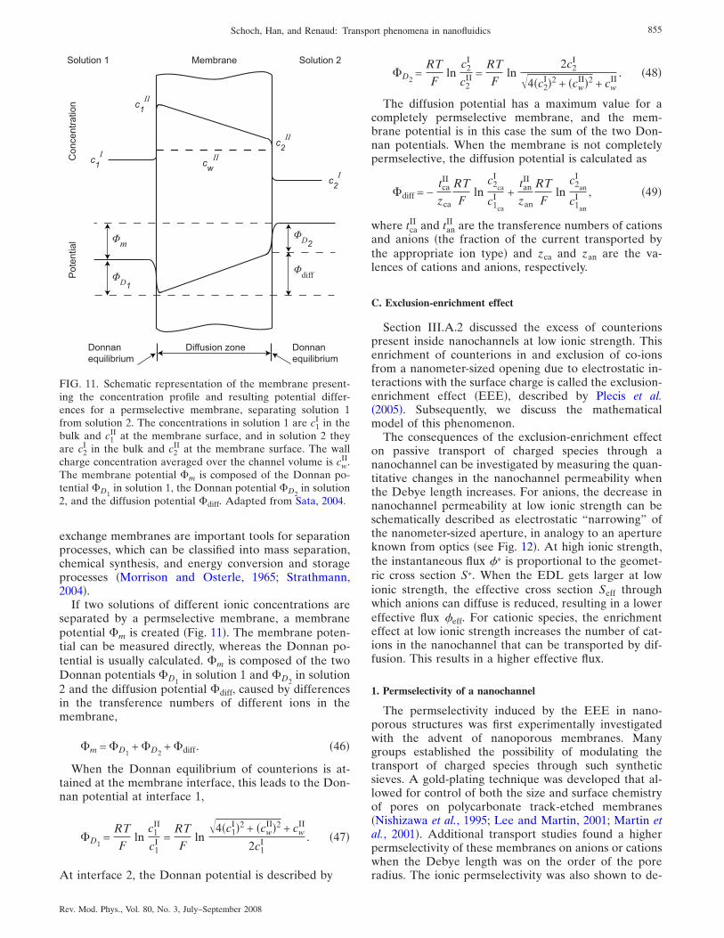
exchange membranes are important tools for separationprocesses, which can be classified into mass separation,chemical synthesis, and energy conversion and storageprocesses �Morrison and Osterle, 1965; Strathmann,2004�.
If two solutions of different ionic concentrations areseparated by a permselective membrane, a membranepotential �m is created �Fig. 11�. The membrane poten-tial can be measured directly, whereas the Donnan po-tential is usually calculated. �m is composed of the twoDonnan potentials �D1
in solution 1 and �D2in solution
2 and the diffusion potential �diff, caused by differencesin the transference numbers of different ions in themembrane,
�m =�D1+�D2
+�diff. �46�
When the Donnan equilibrium of counterions is at-tained at the membrane interface, this leads to the Don-nan potential at interface 1,
�D1=
RT
Fln
c1II
c1I =
RT
Fln
4�c1I�2 + �cw
II�2 + cwII
2c1I . �47�
At interface 2, the Donnan potential is described by
�D2=
RT
Fln
c2I
c2II =
RT
Fln
2c2I
4�c2I�2 + �cw
II�2 + cwII
. �48�
The diffusion potential has a maximum value for acompletely permselective membrane, and the mem-brane potential is in this case the sum of the two Don-nan potentials. When the membrane is not completelypermselective, the diffusion potential is calculated as
�diff = −tcaII
zca
RT
Fln
c2ca
I
c1ca
I +tanII
zan
RT
Fln
c2an
I
c1an
I , �49�
where tcaII and tan
II are the transference numbers of cationsand anions �the fraction of the current transported bythe appropriate ion type� and zca and zan are the va-lences of cations and anions, respectively.
C. Exclusion-enrichment effect
Section III.A.2 discussed the excess of counterionspresent inside nanochannels at low ionic strength. Thisenrichment of counterions in and exclusion of co-ionsfrom a nanometer-sized opening due to electrostatic in-teractions with the surface charge is called the exclusion-enrichment effect �EEE�, described by Plecis et al.�2005�. Subsequently, we discuss the mathematicalmodel of this phenomenon.
The consequences of the exclusion-enrichment effecton passive transport of charged species through ananochannel can be investigated by measuring the quan-titative changes in the nanochannel permeability whenthe Debye length increases. For anions, the decrease innanochannel permeability at low ionic strength can beschematically described as electrostatic “narrowing” ofthe nanometer-sized aperture, in analogy to an apertureknown from optics �see Fig. 12�. At high ionic strength,the instantaneous flux �* is proportional to the geomet-ric cross section S*. When the EDL gets larger at lowionic strength, the effective cross section Seff throughwhich anions can diffuse is reduced, resulting in a lowereffective flux �eff. For cationic species, the enrichmenteffect at low ionic strength increases the number of cat-ions in the nanochannel that can be transported by dif-fusion. This results in a higher effective flux.
1. Permselectivity of a nanochannel
The permselectivity induced by the EEE in nano-porous structures was first experimentally investigatedwith the advent of nanoporous membranes. Manygroups established the possibility of modulating thetransport of charged species through such syntheticsieves. A gold-plating technique was developed that al-lowed for control of both the size and surface chemistryof pores on polycarbonate track-etched membranes�Nishizawa et al., 1995; Lee and Martin, 2001; Martin etal., 2001�. Additional transport studies found a higherpermselectivity of these membranes on anions or cationswhen the Debye length was on the order of the poreradius. The ionic permselectivity was also shown to de-
Membrane Solution 2Solution 1
c1II
c1I
c2II
c2I
cwII
ΦD1
ΦmΦD2
Φdiff
Diffusion zone Donnanequilibrium
Donnanequilibrium
Potential
Concentration
FIG. 11. Schematic representation of the membrane present-ing the concentration profile and resulting potential differ-ences for a permselective membrane, separating solution 1from solution 2. The concentrations in solution 1 are c1
I in thebulk and c1
II at the membrane surface, and in solution 2 theyare c2
I in the bulk and c2II at the membrane surface. The wall
charge concentration averaged over the channel volume is cwII.
The membrane potential �m is composed of the Donnan po-tential �D1
in solution 1, the Donnan potential �D2in solution
2, and the diffusion potential �diff. Adapted from Sata, 2004.
855Schoch, Han, and Renaud: Transport phenomena in nanofluidics
Rev. Mod. Phys., Vol. 80, No. 3, July–September 2008

pend on the surface charge. Positively charged poresshowed increased anion flux compared to negativelycharged pores, and the inverse for cations, which legiti-mizes the idea that the EEE is responsible for this perm-selectivity. Numerical solutions of the fundamental fluxequations by Ramirez, Mafe, Aguilella, et al. �2003� andRamirez, Mafe, Alcarez, et al. �2003� for such mem-branes were compared to experimental results, and wereable to qualitatively explain the observed permselectiv-ity. Practical applications of such permselective mem-branes were investigated by Bluhm et al. �1999� studyingcation transport through positively charged porous alu-mina membranes for the separation of radioactive andhazardous metal cations from contaminated water.
The first quantitative study of the EEE in a nanochan-nel was described by Plecis et al. �2005�, who developeda simple model of the nanochannel permeability forvarying ionic strength. The reference parameter for dif-fusion experiments is the permeability P, which is theconstant that links the instantaneous flux � to the con-centration difference �c,
� = P�c =SD
d�c . �50�
The geometric permeability P* and the geometric crosssection S* characterize the nanochannel when electro-static interactions have a negligible effect on the trans-
port rate �high ionic strength�, whereas the effective per-meability Peff and effective cross section Seff are usedwhen the transport of charged species is affected byelectrostatic forces.
When the exclusion and enrichment of ions occurs atlow ionic strength, the local concentration of chargedspecies is no longer homogeneous in the cross section ofthe nanochannel, because the EDL extension increasesthe counterion concentration near the charged surface.Therefore, the z profile of the local concentration c�x ,z��see Fig. 14� must be averaged to determine the effectiveconcentration ceff�x� in the nanochannel in the presenceof electrostatic forces. The ratio between ceff and c*�x�defines the exclusion-enrichment coefficient �, which isconstant in the whole nanochannel and quantifies theEEE,
� =ceff�x�c*�x�
=�c�x,z��z
c*�x�=
Peff
P*. �51�
The exclusion-enrichment coefficient � is higher than1 in the case of enrichment, and lower than 1 in the caseof exclusion. The measured relative permeability Peff /P*
for different charged probes is shown in Fig. 13, present-ing an exclusion of anions and an enrichment of cations.No change in the permeability has been observed for theneutral probe. Qualitatively, these results are in accor-dance with the main hypothesis that EDL extension re-sults in a higher permeability for counterions and alower permeability for co-ions. However, the change inpermeability is important when 2 Dh before the clas-sical EDL overlap, which means that electrostatic inter-actions between charged species and the walls are im-portant prior to overlap. Moreover, the permeability is
- - - - - - - - - - - - - - - - - - - - -
- - - - - - - - - - - - - - - - - - - - -
- - - - - - - - - - - - - - - - - - - - -
- - - - - - - - - - - - - - - - - - - - -
+ + +++ + +++ + +++ + +++ + +++ + +++
+ + +++ + +++ + +++ + +++ + +++ + +++
++ +
++ +++
++ +++
+ +++++++
++
++
++ +
++ +++
++ +++
+ +++++++
++
++
High ionic strength
Low ionic strength
Ф*S*
Seff
d
-λD
negative surface charge
large diffuse layer
Ф* > Фeff
Z
X
- - ---
--
-
-
--
-- -
-
Фeff
FIG. 12. Schematic of the exclusion effect on anionic trans-port. At high ionic strength, the Debye length is small so thatanions �co-ions� can freely diffuse through the whole cross sec-tion S* of the nanochannel. The instantaneous flux withoutelectrostatic interactions �* is proportional to S*. The Debyelength increases with dilution, reducing the effective cross sec-tion Seff through which anions can diffuse. This results in alower effective flux �eff. Adapted from Plecis et al., 2005.
KCl concentration (M)
Peff/P*
10-5 10-4 10-3 10-2 10-1 100
1
0
2
3
4
5
6experimental cationexperimental neutralexperimental dianion
FIG. 13. Variation of the relative permeability Peff /P* of a50-nm-high nanochannel vs KCl concentration for three probecharges. Marks represent experimental measurements,whereas dotted lines are theoretical fits obtained with Eq. �53�.Anions are excluded from the nanochannel when EDL over-lap occurs at low KCl concentrations, in which regime cationsare attracted, and therefore show enhanced transport throughthe nanochannel. Adapted from Plecis et al., 2005.
856 Schoch, Han, and Renaud: Transport phenomena in nanofluidics
Rev. Mod. Phys., Vol. 80, No. 3, July–September 2008

not zero at low concentrations, which shows that EDLoverlap does not signify complete anion impermeabilityof the nanochannel, as we might suppose from Fig. 12.
2. Model of the exclusion-enrichment effect
At low ionic strength, the EDL thickness becomescomparable to the nanochannel height, resulting in anoverlap of the diffuse parts of the EDLs in thenanometer-sized aperture. It is useful to deduce the po-tential distribution in the case of EDL overlap innanochannels, for which the exact potential is given bythe DLVO theory �see Sec. II.A�. A simplified solutionfor this theory is obtained by solving the Debye-Hückelapproximation given in Eq. �7� with the appropriateboundary conditions, resulting in the following potentialdistribution �Hunter, 1981�:
��z� =� cosh��h/2 − z�/ D�
cosh�h/2 D�. �52�
The numerical solution of the complete Poisson-Boltzmann equation �Eq. �6�� and the approximated po-tential presented in Eq. �52� are compared in Fig. 14�a�for different ionic strengths �Qu and Li, 2000; Conlisk etal., 2002; Conlisk, 2005�. It is known that the Debye-Hückel approximation generally overestimates the elec-tric potential. In order to achieve better precision, nu-merical solution of the Poisson-Boltzmann equationshould be used. However, when the experimental uncer-tainty of permeability measurements is considered, the
difference between the two predicted potentials remainssmall, and the Debye-Hückel approximation is usuallysufficient.
Figure 14�b� shows that at a high ionic strength of0.1M KCl where the potential is zero in most of thenanochannel, no significant change in the concentrationis observed and ceff�x� is equal to c*, except for a negli-gible region near the surface. At low ionic strength,where the electric potential remains high in the wholenanochannel, the exclusion of anionic species and en-richment of cationic probes becomes important. FromEqs. �51�, �52�, and �24�, we obtain an analytical expres-sion for the exclusion-enrichment coefficient,
� =1
h�
0
h
exp�− q�
kBT
cosh��h/2 − z�/ D�cosh�h/2 D� �dz . �53�
Equation �53� shows that the Debye length D and thecharacteristic dimension of the nanochannel h are notthe only parameters characterizing EEE, but the netcharge q of the diffusing species �see Sec. III.D� and the� potential of the surface are also important parametersfor the quantification of this permselective effect. The �potential can be changed with surface charge modifica-tions, and an inversion of the � potential is even possiblewith aluminum pretreatment �Horn and Onoda, 1978;Dilmore et al., 1979�, resulting in an anion-selectivenanochannel �Plecis et al., 2005�.
D. Partitioning at the interface
The transport of large molecules through porousmembranes was initially examined to understand thepermeability of biological structures such as glomerularcapillaries in the kidney, or walls of blood capillaries�Ferry, 1936; Pappenheimer et al., 1951; Renkin, 1954;Cevc, 1990�. Later, renewed interest in fine pores oc-curred when track-etch processes allowed the fabrica-tion of nanopores with better-controlled geometries�Bean et al., 1970�, and models based on the hindereddiffusion of macromolecules through pores had been de-veloped �Beck and Schultz, 1970; Malone and Anderson,1978�. These models include two main sieving contribu-tions: the exclusion of molecules from pores based ongeometric effects and hydrodynamic drag on macromol-ecules due to the proximity of the pore walls. If mol-ecules are comparable in size to the pore, hydrodynamicinteractions between the molecules and pore walls aredependent on long-range intermolecular forces andsteric restrictions. In the 1980s, progress was demon-strated in hindered transport through pores by the quan-tification of electrostatic interactions, the effects of sol-ute concentration on partitioning and transportcoefficients, and the influence of molecular configurationon transport rates �Smith and Deen, 1980; Deen, 1987�.
Hereafter, we present a partitioning theory that ac-counts for size and electrostatic effects, and then we fo-cus on electrostatic sieving. For the discussion of purelysize-dependent sieving, we refer the reader to Sec. IV.B.
z = 0 z = h
ψ(z) in mV
0
ζ=-20
z = 0 z = h
ψ(z) in mV
0
ζ=-60
z = 0 z = h
c(x,z)/c*(x)
10
z = 0 z = h
c(x,z)/c*(x)
10
KCl 0.1 M KCl 0.001 M
(a)
(b)
FIG. 14. Potential and concentration profiles in a 50-nm-highnanochannel for two KCl concentrations. �a� At a low ionicstrength of 0.001M KCl, the potential remains negative in thenanochannel. The difference between the numerical solutionof Eq. �6� �dotted black line� and the approximated analyticalexpression of Eq. �52� �gray solid line� is small. �b� Concentra-tion profiles of charged species are determined by the Boltz-mann equilibrium �Eq. �24��. At low ionic strength, the enrich-ment of cationic species �black solid line, net charge +1e� andthe exclusion of anionic species �gray solid line, net charge−1e� results. Adapted from Plecis et al., 2005.
857Schoch, Han, and Renaud: Transport phenomena in nanofluidics
Rev. Mod. Phys., Vol. 80, No. 3, July–September 2008

1. Partition coefficient for colloids
Smith and Deen �1983� theoretically studied electro-static effects on the partitioning of spherical colloids be-tween a dilute bulk solution and cylindrical pores. Theydefined the fundamental partition coefficient �part, whichexpresses the ratio of the macromolecule concentrationin the pore cm and the bulk cm,b,
�part =cm
cm,b= 2�
0
1−ap/r0
exp� �p�r/r0�kBT
��r/r0�d�r/r0� ,
�54�
where r is the radial coordinate and �p is the potentialenergy of interaction between the colloid and the porewall. Note that the exclusion-enrichment coefficient �assumes a point charge and accounts for electrostaticeffects, compared to the partition coefficient �part, whichalso includes size effects on partitioning. �part has beencalculated by solving the linearized Poisson-Boltzmannequation and determining the free energy of the systemand the interaction potential energy. In cases of solid orcompletely porous spheres and like-charged pores, thecalculated partition coefficients are presented in Fig. 15.This demonstrates that completely porous spheres areelectrostatically less hindered by their transport througha pore than solid spheres, because the elementarycharge is distributed throughout the porous sphere,whereas for solid spheres the same number of chargesreside on the sphere surface. With the increasing ratio ofparticle radius ap to pore radius r0, the exclusion of col-loids from like-charged pores becomes more pro-nounced.
2. Electrostatic sieving of proteins
In reverse osmosis, electrostatic partitioning is used topurify water by applying a pressure gradient over ananoporous membrane, through which only pure watercan pass; negatively charged molecules are rejected atthe entrance of the cation-selective apertures �Smit,1989; Hagmeyer and Gimbel, 1999�. The rejection rateincreases with dilution, resulting in high values at lowionic strength in nanochannels �Schoch, 2006�. Electro-static partitioning can be increased not only by dilution,but also by a higher molecule net charge q, because theexclusion-enrichment coefficient � is exponentially de-pendent on q �see Eq. �53��. Therefore, electrostaticseparation processes are favorable for biomolecules, asdiscussed subsequently, since these molecules typicallybear a high net charge in their native state �Alexov,2004�.
The dominance of electrostatic interaction effects onthe transport of proteins through a nanochannel hasbeen demonstrated by Schoch et al. �2006�. To under-stand their results, it is important to remember that pro-teins possess an isoelectric point �pI� for a characteristicpH value at which they exhibit no net charge. Conse-quently, proteins are amphoteric molecules because theycarry either positive �pHpI�, negative �pH�pI�, orzero net charge �pH=pI�. This fundamental behaviorcan be exploited by changing the pH value of the solu-tion to separate proteins, because the net charge of amolecule affects its diffusion time through a nanochan-nel. Such pH-switchable ion transport has been theoreti-cally described for membranes �Jimbo et al., 2000;Ramirez, Mafe, Alcaraz, et al., 2003�.
In order to demonstrate charge-based transportthrough a nanochannel, three lectin proteins �Foriers etal., 1981� were investigated, which had similar molecularweights of 49 kDa but different pI values of 8.0, 8.2, and8.8 �Schoch et al., 2006�. For these three lectin proteins,the evolution of the apparent diffusion coefficient Dappas the pH of the solution is varied between 6 and 11 isshown in Fig. 16. The curve illustrates three zones: forpH�7 and pH 9, the diffusion of lectin through thenanochannel is slow, whereas the diffusion is signifi-cantly faster for pH values between 7 and 9. Threepeaks are visible in this part of the curve, one at pH=7.5, a second at pH=8.2, and a third at pH=8.8, andthey can be attributed to the pI values of the three pro-teins, showing a maximal diffusion coefficient throughthe nanochannel if they are neutral and do not haveelectrostatic interactions with channel walls �Burns andZydney, 1999; Chun and Stroeve, 2002; Ku and Stroeve,2004�. For pH 9, all three proteins are negativelycharged and excluded from the nanochannel accordingto the EEE �Eq. �53��. Based on the exclusion-enrichment effect, low diffusion times are expected forpH�7, when proteins are positively charged and conse-quently attracted by the nanochannel, but low apparentdiffusion coefficients have been measured for this zone.To elucidate this discrepancy, the protein concentrationin the nanochannel has been measured between pH 6
8
ap/r0 = 0.2
ap/r0 = 0.4
ap/r0 = 0.6
16 24 32 400
0.6
0.4
0.2
r0 / λD
c (M)0.001 0.01 0.05 0.1 0.2 0.3
βpart
P
P
PS
S
S
FIG. 15. Partition coefficient �part as a function of the solutionconcentration c, or of the ratio of pore radius r0 to Debyelength D, for completely porous �P� and solid �S� spheres ofidentical size and total charge. Calculations were performedfor r0=20 nm, surface charge densities of walls and spheres of0.01 C m−2, and a 1:1 univalent electrolyte. Dashed lines indi-cate that asymptotic values are approached at high ionicstrength for each value of ap /r0, where ap is the particle radius.Adapted from Smith and Deen, 1983.
858 Schoch, Han, and Renaud: Transport phenomena in nanofluidics
Rev. Mod. Phys., Vol. 80, No. 3, July–September 2008
and 11, showing maximum values for pH�7. Thus, itwas concluded that proteins steadily enter the channel,but can hardly leave because they are retarded and re-versibly adsorbed on the nanochannel walls �Gray, 2004;Lionello et al., 2005�. The reversible adsorption of pro-teins to the surfaces also occurs between pH 7 and 9,which leads to a slight pH change in the nanochannelbecause the local electrochemical potential near the pro-tein regulates the ionizable surface group dissociationrather than the bulk chemical potential �Bostrom et al.,2005�. These results confirm that adsorption and desorp-tion kinetics become important in nanochannels �Drazeret al., 2002; Baldessari and Santiago, 2006�.
(a) Considerations. Decreased diffusion coefficients ofa protein for pH values below its pI were first measuredin nanoporous membranes. Ku and Stroeve �2004� ar-gued that at pH values below the pI, the protein adsorbson the nanopore surface. Additionally, the negativecounterions of the positively charged protein are re-pelled from the negatively charged nanopores. Thisleads to the creation of a diffusion potential inside thenanopores that retards protein transport. Another ex-planation given by Burns and Zydney �1999� describesthe energetic penalty associated with the distortion ofthe EDL around the charged protein by the channelwall. This distortion leads to net repulsive interactions,even when protein and pores have opposite charges. Thethird explanation is the charge regulation of biomol-ecules, which originates from the protein charge, which
is not constant but affected by nearby charged objects�Stahlberg and Jonsson, 1996; Pujar and Zydney, 1997;Zydney and Pujar, 1998; Menon and Zydney, 2000;Gohda and Pantelides, 2005; Lund et al., 2005�. As aprotein comes close to an oppositely charged stationarysurface, the protein net charge will change because ofthe electric field from the surface.
(b) Protein adsorption. The adsorption of proteinsfrom a solution to a surface is affected by many param-eters �Norde, 1986; Nakanishi et al., 2001� and remains acontroversial problem today. Polymers that resist pro-tein adsorption are relevant for biomedical and bioana-lytical applications. Poly�L-lysine� grafted with poly�eth-ylene glycol� �PLL-g-PEG� is a promising polymer toreduce nonspecific binding �Kenausis et al., 2000; Huang,Voros, De Paul, et al., 2002�, and this has been verified inmicrofluidic devices �Marie et al., 2006�.
3. Active control of partitioning
Partitioning can be controlled actively with field ef-fects �Ghowsi and Gale, 1991; Schasfoort et al., 1999�,which has been shown in nanochannels using externalelectrodes �Schoch and Renaud, 2005�. Karnik, Fan,Yue, et al. �2005� and Karnik, Castelino, and Majumdar�2006� demonstrated that, similar to a field-effect tran-sistor, a gate electrode on nanofluidic channels can beused to change their surface charge, enabling field-effectcontrol as shown in Fig. 17. When the gate voltage Vg ispositive, only negatively charged molecules can diffuseacross the nanochannels, and positively charged biomol-ecules are excluded. It has been proposed that such de-vices do not require EDL overlap �Stein et al., 2004;Daiguji et al., 2005�. Unlike metal-coated nanoporousmembranes, where the transport can be controlled bychanging the potential applied to the membrane surface�Nishizawa et al., 1995; Chun et al., 2006�, nanofluidicchannels with a gate voltage enable researchers to ad-dress individual nanometer-sized openings.
pH
6 7 8 9 10 11
Dapp(m2s-1 )
La LbLm
FIG. 16. Apparent diffusion coefficient Dapp of three lectinproteins as a function of the pH value of the solution, mea-sured in a 50-nm-high nanochannel at an ionic strength of10−3M. Dapp of the three lectin proteins shows three peaks,corresponding to the pI values of the acidic band lectin La, themiddle band lectin Lm, and the basic band lectin Lb. Themarks on the pH axis show the respective pI values of thelectins, which have been measured with isoelectric focusing.The connecting lines are for guidance only. From Schoch et al.,2006.
(a) (b)
FIG. 17. Nanofluidic control of protein transport by a gatevoltage without bias between the microchannels. When thegate voltage Vg is negative, the positively charged protein avi-din can diffuse through the nanochannel, whereas the proteinis repelled when Vg is positive. �a� Schematics and �b� corre-sponding fluorescence images. Adapted from Karnik, Cas-telino, and Majumdar, 2006.
859Schoch, Han, and Renaud: Transport phenomena in nanofluidics
Rev. Mod. Phys., Vol. 80, No. 3, July–September 2008

Tunable ionic transport has been demonstrated by theapplication of a potential difference over a membrane�Schmuhl et al., 2004, 2005�, which we investigate fornanochannels on a chip.
E. Concentration polarization
When an external electric field is applied through ananochannel, electrokinetic transport is superimposedon diffusion. This ionic current transport can induceconsiderable forces on electrolytes in nanometer-sizedapertures, as a result of which convection has to be con-sidered �Helfferich, 1962�. Concentration polarizationdoes occur under these conditions, as well as a complexset of effects related to the formation of ionic concen-tration gradients in the electrolyte solution adjacent toan ion-selective interface. Such phenomena are compli-cated, and current electrokinetic theory �based on theequilibrium model of EDL� is inadequate to describethe complexity of the physics therein.
Subsequently, we describe fundamental aspects ofconcentration polarization and how these effects can beexploited for applications such as the preconcentrationof molecules. A comprehensive review of nanoporeionic conductance in micrometer-scale analysis systemshas recently been presented �Holtzel and Tallarek,2007�, and a detailed analysis of bulk concentration po-larization for a two-parallel-plate electrode model withsuddenly applied electric fields was provided by Bazantet al. �2004�.
In solution, the electric current is transmitted by bothanions and cations, and their transference number �seeSec. III.B.2� is about 0.5 for both ion types. However, inan ion-selective nanochannel, the current is mainlytransported by counterions, resulting in a transferencenumber close to 1. At the anodic side of a cation-selective nanochannel �see Fig. 18�, the concentration ofions in solution is reduced because of the lower trans-
port number of cations in the solution relative to that inthe nanometer-sized opening �Strathmann, 2004; Nis-chang et al., 2006�. Anions move in the opposite direc-tion and cannot be compensated by the few anions thatremain in the nanochannel. Because of electroneutrality,cations and anions are reduced by the same amount infront of the nanochannel on the anodic side, where aconcentration gradient is established. At the other sideof the nanochannel facing the cathodic side, cations ac-cumulate because more cations are transferred throughthe nanochannel than are carried away by the electriccurrent. The transference number of anions in thenanochannel is almost zero, resulting in their accumula-tion at the cathodic side of the nanometer-sized aperture�Petersen et al., 2004�.
The concentration polarization is schematically pre-sented in Fig. 18, which shows that cations are mainlytransported by migrational flux Jca
mig through thenanometer-sized opening. Anions are largely excludedand their flux through the nanochannel is small com-pared to cation flux. The diffusional flux of salt Js
diff, in-cluding cations and anions, follows the gradient from theconcentrate toward the dilute side. In the diffusionboundary layer �DBL� at both sides of the nanometer-sized aperture, cations and anions are transported by themigrational fluxes Jca
mig and Janmig, respectively, which are
in opposing directions and thus generate a concentrationgradient. This concentration gradient leads to a diffu-sional flux of salt Js
diff, which is oriented toward thenanochannel on the dilute side and the bulk solution onthe concentrated side of the nanochannel.
1. Limiting current through nanochannels
Concentration polarization can lead to a high salt con-centration on the cathodic side of a nanochannel, and ifit exceeds the solubility limits of the solution constitu-ents, precipitation of salts may occur, resulting in an ad-ditional electric resistance. On the contrary, if the saltconcentration is reduced to zero on the anodic side ofthe nanometer-sized opening, there are no ions availableto carry the electric current. This results in a limitedcurrent Ilim, which corresponds to region II in Fig. 19. Tocalculate this limited current, the electrochemical analogto Fick’s first law is considered �refer to Eq. �36��,
I = nFAD�c
�x. �55�
The concentration gradient is commonly approxi-mated by a linear extrapolation of the slope c versus x tox=0 �Rubinstein, 1995�,
I = nFADcb − c�x = 0�
!, �56�
where cb is the bulk concentration and ! is the DBLthickness present at solid-liquid interfaces �Levich, 1962;Cussler, 1997�. For porous membranes, ! is typically be-tween 10 and 400 �m �Yaroshchuk et al., 2005�. At themicrochannel-nanochannel interface, it is assumed that
DBL
nanochannel
diluatebulk solution
concentratebulk solution
anode
cathode
Jcamig
Janmig
Jcamig
Janmig
Jsdiff
Jsdiff
bucsdi
nanocsdi
nanocsco
bucsco Jca
mig
DBL
Jsdiff
FIG. 18. Schematic illustrating concentration polarization atnanochannel interfaces. Concentration profiles of salt in thediffusion boundary layer �DBL� on both sides of the cation-selective nanochannel are presented, as well as the fluxes perarea J of cations �ca�, anions �an�, and salt �s� in the DBL andin the nanochannel. The superscripts mig and diff refer to mi-gration and diffusion, di and co refer to dilute and concentratesolutions, and bu and nano refer to bulk phase and nanochan-nel interface, respectively. Adapted from Strathmann, 2004.
860 Schoch, Han, and Renaud: Transport phenomena in nanofluidics
Rev. Mod. Phys., Vol. 80, No. 3, July–September 2008
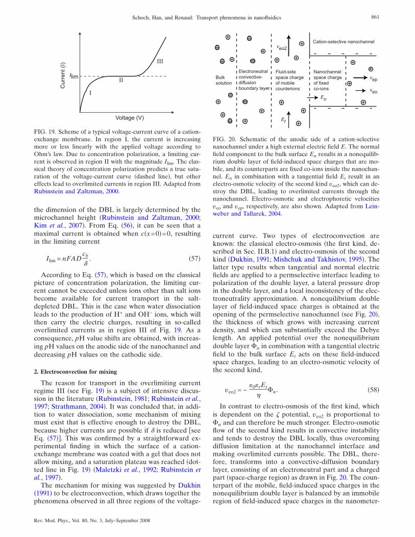
the dimension of the DBL is largely determined by themicrochannel height �Rubinstein and Zaltzman, 2000;Kim et al., 2007�. From Eq. �56�, it can be seen that amaximal current is obtained when c�x=0�=0, resultingin the limiting current
Ilim = nFADcb
!. �57�
According to Eq. �57�, which is based on the classicalpicture of concentration polarization, the limiting cur-rent cannot be exceeded unless ions other than salt ionsbecome available for current transport in the salt-depleted DBL. This is the case when water dissociationleads to the production of H+ and OH− ions, which willthen carry the electric charges, resulting in so-calledoverlimited currents as in region III of Fig. 19. As aconsequence, pH value shifts are obtained, with increas-ing pH values on the anodic side of the nanochannel anddecreasing pH values on the cathodic side.
2. Electroconvection for mixing
The reason for transport in the overlimiting currentregime III �see Fig. 19� is a subject of intensive discus-sion in the literature �Rubinstein, 1981; Rubinstein et al.,1997; Strathmann, 2004�. It was concluded that, in addi-tion to water dissociation, some mechanism of mixingmust exist that is effective enough to destroy the DBL,because higher currents are possible if ! is reduced �seeEq. �57��. This was confirmed by a straightforward ex-perimental finding in which the surface of a cation-exchange membrane was coated with a gel that does notallow mixing, and a saturation plateau was reached �dot-ted line in Fig. 19� �Maletzki et al., 1992; Rubinstein etal., 1997�.
The mechanism for mixing was suggested by Dukhin�1991� to be electroconvection, which draws together thephenomena observed in all three regions of the voltage-
current curve. Two types of electroconvection areknown: the classical electro-osmosis �the first kind, de-scribed in Sec. II.B.1� and electro-osmosis of the secondkind �Dukhin, 1991; Mishchuk and Takhistov, 1995�. Thelatter type results when tangential and normal electricfields are applied to a permselective interface leading topolarization of the double layer, a lateral pressure dropin the double layer, and a local inconsistency of the elec-troneutrality approximation. A nonequilibrium doublelayer of field-induced space charges is obtained at theopening of the permselective nanochannel �see Fig. 20�,the thickness of which grows with increasing currentdensity, and which can substantially exceed the Debyelength. An applied potential over the nonequilibriumdouble layer �n in combination with a tangential electricfield to the bulk surface Et acts on these field-inducedspace charges, leading to an electro-osmotic velocity ofthe second kind,
veo2 = −0rEt
��n. �58�
In contrast to electro-osmosis of the first kind, whichis dependent on the � potential, veo2 is proportional to�n and can therefore be much stronger. Electro-osmoticflow of the second kind results in convective instabilityand tends to destroy the DBL locally, thus overcomingdiffusion limitation at the nanochannel interface andmaking overlimited currents possible. The DBL, there-fore, transforms into a convective-diffusion boundarylayer, consisting of an electroneutral part and a chargedpart �space-charge region� as drawn in Fig. 20. The coun-terpart of the mobile, field-induced space charges in thenonequilibrium double layer is balanced by an immobileregion of field-induced space charges in the nanometer-
Voltage (V)
Current(I)
Ilim II
III
I
FIG. 19. Scheme of a typical voltage-current curve of a cation-exchange membrane. In region I, the current is increasingmore or less linearly with the applied voltage according toOhm’s law. Due to concentration polarization, a limiting cur-rent is observed in region II with the magnitude Ilim. The clas-sical theory of concentration polarization predicts a true satu-ration of the voltage-current curve �dashed line�, but othereffects lead to overlimited currents in region III. Adapted fromRubinstein and Zaltzman, 2000.
Cation-selective nanochannel
Nanochannelspace chargeof fixedco-ions
Fluid-sidespace chargeof mobilecounterions
Electroneutralconvective-diffusionboundary layer
Bulksolution
Et
En
vep
veo
veo2
FIG. 20. Schematic of the anodic side of a cation-selectivenanochannel under a high external electric field E. The normalfield component to the bulk surface En results in a nonequilib-rium double layer of field-induced space charges that are mo-bile, and its counterparts are fixed co-ions inside the nanochan-nel. En in combination with a tangential field Et result in anelectro-osmotic velocity of the second kind veo2, which can de-stroy the DBL, leading to overlimited currents through thenanochannel. Electro-osmotic and electrophoretic velocitiesveo and vep, respectively, are also shown. Adapted from Lein-weber and Tallarek, 2004.
861Schoch, Han, and Renaud: Transport phenomena in nanofluidics
Rev. Mod. Phys., Vol. 80, No. 3, July–September 2008
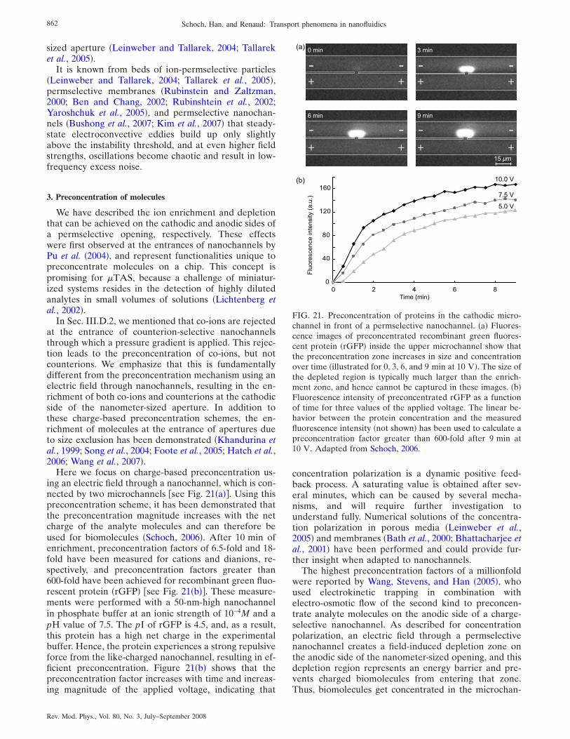
sized aperture �Leinweber and Tallarek, 2004; Tallareket al., 2005�.
It is known from beds of ion-permselective particles�Leinweber and Tallarek, 2004; Tallarek et al., 2005�,permselective membranes �Rubinstein and Zaltzman,2000; Ben and Chang, 2002; Rubinshtein et al., 2002;Yaroshchuk et al., 2005�, and permselective nanochan-nels �Bushong et al., 2007; Kim et al., 2007� that steady-state electroconvective eddies build up only slightlyabove the instability threshold, and at even higher fieldstrengths, oscillations become chaotic and result in low-frequency excess noise.
3. Preconcentration of molecules
We have described the ion enrichment and depletionthat can be achieved on the cathodic and anodic sides ofa permselective opening, respectively. These effectswere first observed at the entrances of nanochannels byPu et al. �2004�, and represent functionalities unique topreconcentrate molecules on a chip. This concept ispromising for �TAS, because a challenge of miniatur-ized systems resides in the detection of highly dilutedanalytes in small volumes of solutions �Lichtenberg etal., 2002�.
In Sec. III.D.2, we mentioned that co-ions are rejectedat the entrance of counterion-selective nanochannelsthrough which a pressure gradient is applied. This rejec-tion leads to the preconcentration of co-ions, but notcounterions. We emphasize that this is fundamentallydifferent from the preconcentration mechanism using anelectric field through nanochannels, resulting in the en-richment of both co-ions and counterions at the cathodicside of the nanometer-sized aperture. In addition tothese charge-based preconcentration schemes, the en-richment of molecules at the entrance of apertures dueto size exclusion has been demonstrated �Khandurina etal., 1999; Song et al., 2004; Foote et al., 2005; Hatch et al.,2006; Wang et al., 2007�.
Here we focus on charge-based preconcentration us-ing an electric field through a nanochannel, which is con-nected by two microchannels �see Fig. 21�a��. Using thispreconcentration scheme, it has been demonstrated thatthe preconcentration magnitude increases with the netcharge of the analyte molecules and can therefore beused for biomolecules �Schoch, 2006�. After 10 min ofenrichment, preconcentration factors of 6.5-fold and 18-fold have been measured for cations and dianions, re-spectively, and preconcentration factors greater than600-fold have been achieved for recombinant green fluo-rescent protein �rGFP� �see Fig. 21�b��. These measure-ments were performed with a 50-nm-high nanochannelin phosphate buffer at an ionic strength of 10−4M and apH value of 7.5. The pI of rGFP is 4.5, and, as a result,this protein has a high net charge in the experimentalbuffer. Hence, the protein experiences a strong repulsiveforce from the like-charged nanochannel, resulting in ef-ficient preconcentration. Figure 21�b� shows that thepreconcentration factor increases with time and increas-ing magnitude of the applied voltage, indicating that
concentration polarization is a dynamic positive feed-back process. A saturating value is obtained after sev-eral minutes, which can be caused by several mecha-nisms, and will require further investigation tounderstand fully. Numerical solutions of the concentra-tion polarization in porous media �Leinweber et al.,2005� and membranes �Bath et al., 2000; Bhattacharjee etal., 2001� have been performed and could provide fur-ther insight when adapted to nanochannels.
The highest preconcentration factors of a millionfoldwere reported by Wang, Stevens, and Han �2005�, whoused electrokinetic trapping in combination withelectro-osmotic flow of the second kind to preconcen-trate analyte molecules on the anodic side of a charge-selective nanochannel. As described for concentrationpolarization, an electric field through a permselectivenanochannel creates a field-induced depletion zone onthe anodic side of the nanometer-sized opening, and thisdepletion region represents an energy barrier and pre-vents charged biomolecules from entering that zone.Thus, biomolecules get concentrated in the microchan-
Fluorescenceintensity(a.u.)
0
40
80
120
160
0 2 4 6 8
10.0 V
7.5 V
5.0 V
Time (min)
0 min 3 min
- -++
- -++
(a)
(b)
6 min
- -++
9 min
- -++
15 μm
FIG. 21. Preconcentration of proteins in the cathodic micro-channel in front of a permselective nanochannel. �a� Fluores-cence images of preconcentrated recombinant green fluores-cent protein �rGFP� inside the upper microchannel show thatthe preconcentration zone increases in size and concentrationover time �illustrated for 0, 3, 6, and 9 min at 10 V�. The size ofthe depleted region is typically much larger than the enrich-ment zone, and hence cannot be captured in these images. �b�Fluorescence intensity of preconcentrated rGFP as a functionof time for three values of the applied voltage. The linear be-havior between the protein concentration and the measuredfluorescence intensity �not shown� has been used to calculate apreconcentration factor greater than 600-fold after 9 min at10 V. Adapted from Schoch, 2006.
862 Schoch, Han, and Renaud: Transport phenomena in nanofluidics
Rev. Mod. Phys., Vol. 80, No. 3, July–September 2008

nel at the interface to the depletion region. A secondelectric field gradient has been applied along the anodicmicrochannel, which leads to an electro-osmotic flow ofthe second kind in this channel, and hence supplies thepreconcentration zone efficiently with biomolecules.This electrokinetic trapping and collection procedurecan be run for several hours, allowing high preconcen-tration factors.
IV. MACROMOLECULE SEPARATION MECHANISMSUSING NANOMETER-SIZED STRUCTURES
During the past several years, significant interest hasemerged in separating macromolecules, and it has beendemonstrated that nanofluidics can accomplish this taskby exploiting various mechanisms. In this section, wereport the physical principles of separation mechanismsusing nanometer-sized structures on a chip, which repre-sents a growing field with potential applications for�TAS �He et al., 1998; Eijkel and van den Berg, 2006;Haber, 2006�. Such microfabricated regular sieving struc-tures hold promise as an alternative to gels or capillariesto improve biomolecule separation speed and reso-lution. Until recently, the main focus has been placed onthe separation of long DNA molecules �Chou et al.,2000� due to the Human Genome Project �Craig Venteret al., 2001; Lander et al., 2001�, limitations in gel elec-trophoresis �Turmel et al., 1990; Gygi et al., 2000; Lam-bert et al., 2005�, and well-known DNA separation phys-ics �Giddings, 1965, 1991; de Gennes, 1979; Stellwagen etal., 1997; Righetti et al., 2002; Slater et al., 2003�. Theinterest in separation techniques for smaller physiologi-cally relevant biomolecules is increasing �Corthals et al.,1997; Anderson and Anderson, 1998; Rabilloud, 2002;Freire and Wheeler, 2006�.
A. Entropic trapping
When a DNA molecule is in a relaxed state and inequilibrium, it has a spherical shape with a radius ofgyration R0. However, if the molecule is forced into anopening with dimensions smaller than 2R0, it has to de-form from its state of minimal energy. The entry of theDNA strand into such a constricted space is called en-tropic trapping �Muthukumar and Baumgartner, 1989;Smisek and Hoagland, 1990; Rousseau et al., 1997�, andthe entropic trapping effect of polymer chains in micro-fabricated structures has been directly observed �Hanand Craighead, 1999, 2000; Han et al., 1999�.
Han and Craighead �2000� used a nanofilter columnconsisting of alternating deep regions �td2 �m� andshallow constrictions �ts90 nm�, over which an electricfield was applied �see Fig. 22�a��. It has been demon-strated that longer DNA molecules move faster throughthe column because they have a better chance of escap-ing entropic traps. This is due to the larger contact areaof the DNA molecule with the thin region �Fig. 22�b��,which results in a shorter entropic trapping lifetime. Animportant parameter describing the trapping lifetime isthe magnitude of the electric field in the nanochannel
Es, because the necessary energy to overcome an en-tropic trap ��max is proportional to 1/Es �Fig. 22�d��. Thetrapping lifetime " for intermediate electric fields���maxkBT� is
" = "0 exp���max/kBT� = "0 exp��/EskBT� , �59�
where "0 is the trapping lifetime at high electric fields.Han and Craighead �2002� optimized all parameters
affecting the separation of long DNA molecules acrossentropic traps. The outcome of this study was that evenmega-base-pair DNA strands can be separated aboutten times faster with entropic traps than with conven-tional pulsed field gel electrophoresis. Simulations of thetrapping lifetime as a function of molecular size andelectric field strength have been presented by Tessierand Slater �2002� and Tessier et al. �2002�.
B. Ogston sieving
Ogston sieving �Ogston, 1958; Rodbard and Chram-bach, 1970� is fundamental for describing the mobility ofglobular molecules in gel electrophoresis, which iswidely used to separate molecules by size �Giddings etal., 1968; de Gennes, 1971; Semenov et al., 1995; Viovy,2000; Slater et al., 2002�. The sieving mechanism is de-scribed by a partitioning process �see Sec. III.D� due to
(a)
(b)
(d)
E fieldlines
td
ts
xf
E=EsE=Ed
DNA xf
∆ transition state
∆ max~1/Esxf,c ~1/Estrapped state
(c)
DNACathode(-)
Thick region Thin region
Anode(+)
30µm a
b
wawb
ts = 75~100nmtd = 1.5~3µm
2Ra
DNAmotion
FIG. 22. Entropic trapping of DNA in a nanofilter column. �a�Cross-sectional schematic of the device consisting of alternat-ing shallow �ts� and deep �td� regions. Electrophoresed DNAmolecules are trapped whenever they meet a thin region. �b�Top view of the device. The width w of the DNA molecule incontact with the thin region determines the trapping lifetime,and therefore the overall mobility. R0 is the radius of gyration.From Han and Craighead, 2000. �c� Escape of a DNA mol-ecule from the trap, where xf is the length of the DNA strandin the filter. �d� Energy �� vs xf. The transition state at whichthe strands overcome the energy barrier is when xf=xf,c.Adapted from Han et al., 1999.
863Schoch, Han, and Renaud: Transport phenomena in nanofluidics
Rev. Mod. Phys., Vol. 80, No. 3, July–September 2008
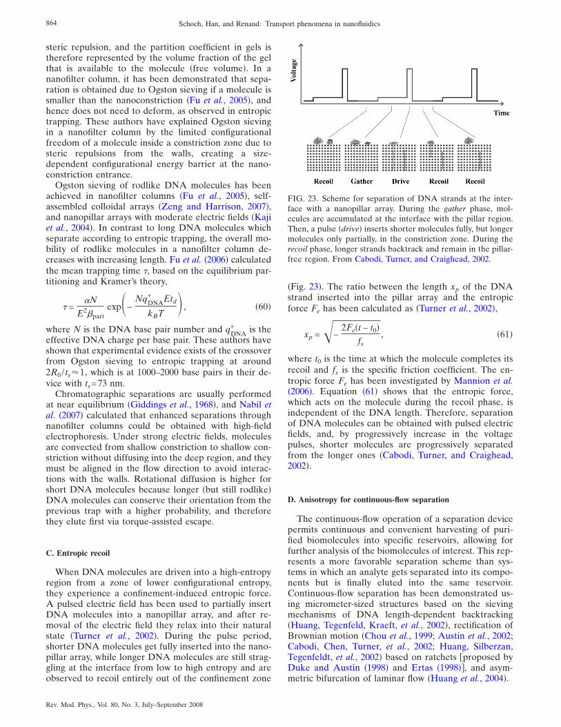
steric repulsion, and the partition coefficient in gels istherefore represented by the volume fraction of the gelthat is available to the molecule �free volume�. In ananofilter column, it has been demonstrated that sepa-ration is obtained due to Ogston sieving if a molecule issmaller than the nanoconstriction �Fu et al., 2005�, andhence does not need to deform, as observed in entropictrapping. These authors have explained Ogston sievingin a nanofilter column by the limited configurationalfreedom of a molecule inside a constriction zone due tosteric repulsions from the walls, creating a size-dependent configurational energy barrier at the nano-constriction entrance.
Ogston sieving of rodlike DNA molecules has beenachieved in nanofilter columns �Fu et al., 2005�, self-assembled colloidal arrays �Zeng and Harrison, 2007�,and nanopillar arrays with moderate electric fields �Kajiet al., 2004�. In contrast to long DNA molecules whichseparate according to entropic trapping, the overall mo-bility of rodlike molecules in a nanofilter column de-creases with increasing length. Fu et al. �2006� calculatedthe mean trapping time ", based on the equilibrium par-titioning and Kramer’s theory,
" =�N
E2�partexp�−
NqDNA* Etd
kBT� , �60�
where N is the DNA base pair number and qDNA* is the
effective DNA charge per base pair. These authors haveshown that experimental evidence exists of the crossoverfrom Ogston sieving to entropic trapping at around2R0 / ts1, which is at 1000–2000 base pairs in their de-vice with ts=73 nm.
Chromatographic separations are usually performedat near equilibrium �Giddings et al., 1968�, and Nabil etal. �2007� calculated that enhanced separations throughnanofilter columns could be obtained with high-fieldelectrophoresis. Under strong electric fields, moleculesare convected from shallow constriction to shallow con-striction without diffusing into the deep region, and theymust be aligned in the flow direction to avoid interac-tions with the walls. Rotational diffusion is higher forshort DNA molecules because longer �but still rodlike�DNA molecules can conserve their orientation from theprevious trap with a higher probability, and thereforethey elute first via torque-assisted escape.
C. Entropic recoil
When DNA molecules are driven into a high-entropyregion from a zone of lower configurational entropy,they experience a confinement-induced entropic force.A pulsed electric field has been used to partially insertDNA molecules into a nanopillar array, and after re-moval of the electric field they relax into their naturalstate �Turner et al., 2002�. During the pulse period,shorter DNA molecules get fully inserted into the nano-pillar array, while longer DNA molecules are still strag-gling at the interface from low to high entropy and areobserved to recoil entirely out of the confinement zone
�Fig. 23�. The ratio between the length xp of the DNAstrand inserted into the pillar array and the entropicforce Fe has been calculated as �Turner et al., 2002�,
xp =−2Fe�t − t0�
fs, �61�
where t0 is the time at which the molecule completes itsrecoil and fs is the specific friction coefficient. The en-tropic force Fe has been investigated by Mannion et al.�2006�. Equation �61� shows that the entropic force,which acts on the molecule during the recoil phase, isindependent of the DNA length. Therefore, separationof DNA molecules can be obtained with pulsed electricfields, and, by progressively increase in the voltagepulses, shorter molecules are progressively separatedfrom the longer ones �Cabodi, Turner, and Craighead,2002�.
D. Anisotropy for continuous-flow separation
The continuous-flow operation of a separation devicepermits continuous and convenient harvesting of puri-fied biomolecules into specific reservoirs, allowing forfurther analysis of the biomolecules of interest. This rep-resents a more favorable separation scheme than sys-tems in which an analyte gets separated into its compo-nents but is finally eluted into the same reservoir.Continuous-flow separation has been demonstrated us-ing micrometer-sized structures based on the sievingmechanisms of DNA length-dependent backtracking�Huang, Tegenfeld, Kraeft, et al., 2002�, rectification ofBrownian motion �Chou et al., 1999; Austin et al., 2002;Cabodi, Chen, Turner, et al., 2002; Huang, Silberzan,Tegenfeldt, et al., 2002� based on ratchets �proposed byDuke and Austin �1998� and Ertas �1998��, and asym-metric bifurcation of laminar flow �Huang et al., 2004�.
FIG. 23. Scheme for separation of DNA strands at the inter-face with a nanopillar array. During the gather phase, mol-ecules are accumulated at the interface with the pillar region.Then, a pulse �drive� inserts shorter molecules fully, but longermolecules only partially, in the constriction zone. During therecoil phase, longer strands backtrack and remain in the pillar-free region. From Cabodi, Turner, and Craighead, 2002.
864 Schoch, Han, and Renaud: Transport phenomena in nanofluidics
Rev. Mod. Phys., Vol. 80, No. 3, July–September 2008

We have discussed mechanisms that can separatelarge macromolecules, and their applicability to smaller,physiologically relevant macromolecules remains ques-tionable �Austin et al., 2002; Huang, Silberzan, Tegen-feldt, et al., 2002�. To overcome this limitation, the prop-erties of an anisotropic nanofluidic array have beenexploited by Fu et al. �2007� to separate short DNA andproteins under native conditions in continuous flow. Theanisotropy relies on different sieving characteristicsalong two orthogonal directions x and y within the array,where only deep channels are designed in the y direc-tion, while the x direction consists of alternating deepchannels and shallow nanofluidic constrictions �see Fig.24�. Two orthogonal electric fields Ex and Ey are used todrive the molecules through the channels.
This unique molecular sieving structure has demon-strated continuous-flow separation of DNA and proteinsbased on either size or charge �Fu et al., 2007�. The shal-low nanofluidic channels represent energy barriers toboth steric and electrostatic interactions betweencharged biomolecules and charged nanofilter walls, re-sulting in the sieving mechanisms of Ogston sieving �seeSec. IV.B�, entropic trapping �see Sec. IV.A�, or electro-static sieving �see Sec. III.D.2�. Size-based separationsdue to Ogston sieving and entropic trapping are per-formed at high ionic strength, where the Debye length D is negligible compared to the nanofilter shallow re-gion ts, whereas low-ionic-strength solutions, when Dbecomes comparable to ts, are used for electrostatic siev-ing. The separation of differently sized or charged bio-molecules is obtained because macromolecules have dif-ferent mean characteristic drift distances L in the deepchannels between two consecutive nanofilter crossings,leading to distinct stream deflection angles # and jumppassage rates Px �see Fig. 24�.
V. NANOPORES AND NANOWIRES FOR LABEL-FREEBIOMOLECULE DETECTION
There are two main types of detection methods thatare commonly integrated into �TAS: fluorescent andelectrical detections. Optical approaches are straightfor-ward and provide direct visual proof. But with regard toindustrial applications, a lab-on-a-chip device should beinexpensive, and electronic sensors are therefore favor-able. Additionally, electrical characterizations do not re-quire fluorescent dyes, which can cause variations in thenet charge, conformational changes, or steric hindranceof the analyte �Richards et al., 1999; Ramachandran etal., 2005�. In this section, we present promising electricaland label-free biomolecule detection methods, which arebased on nanofluidic objects such as nanopores andnanowires.
A. Biomolecule translocations through nanopores
Kasianowicz et al. �1996� demonstrated that a DNAmolecule can be detected as a transient decrease in theionic current when it passes through a nanopore, and thepassage duration allows for the determination of poly-mer length. If each base in the DNA molecule were tomodulate the signal in a specific and measurable wayduring translocation, then the base sequence could bedetermined at rates between 1000 and 10 000 bases persecond �Deamer and Akeson, 2000�. Thus, the ultimategoal of this technique is to realize rapid DNA sequenc-ing �Howorka et al., 2001; Wang and Branton, 2001;Meller, 2003; Ashkenasy et al., 2005; Chan, 2005�.
It has been proposed that the required measurementsensitivity to distinguish individual bases might beachievable with embedded electrodes in the walls alongthe axis of a synthetic nanopore �Lagerqvist et al., 2006�.However, the transverse conductance across DNA frag-ments between electrodes depends critically on geomet-
tdx
y
Ogston sievingts
Electrostatic sieving
λD
λD
Thick regionThin regionSilicon pillar
λD
Entropic trapping
Px
Px
Px
Ex
Ey
Lθ
Ex
Ey
Ex
Ey
(a)
(b)
(c)
FIG. 24. Bidirectional motion of negatively charged macro-molecules in an anisotropic nanofilter array, driven by two or-thogonal electric fields Ex and Ey. �a� Ogston sieving and �b�entropic trapping are obtained when D� ts. In this regime athigh ionic strength, steric interactions dictate the jump dynam-ics and the passage rate Px. �c� Electrostatic sieving becomesdominant when D ts. The mean drift distance L plays a de-terminant role for the migration trajectory, with a shorter Lleading to a larger stream deflection angle #, where # is definedwith respect to the positive y axis. Silicon pillars serve as sup-porting structures to prevent collapse of the top ceiling.Adapted from Fu et al., 2007.
865Schoch, Han, and Renaud: Transport phenomena in nanofluidics
Rev. Mod. Phys., Vol. 80, No. 3, July–September 2008
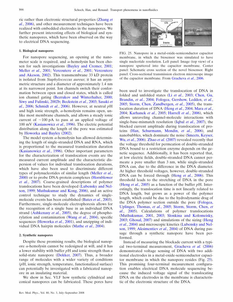
ric rather than electronic structural properties �Zhang etal., 2006�, and other measurement techniques have beenrealized with embedded electrodes in the nanopores. Wefurther present interesting effects of biological and syn-thetic nanopores, which have been observed on the wayto electrical DNA sequencing.
1. Biological nanopores
For nanopore sequencing, an opening at the nano-meter scale is required, and �-hemolysin has been cho-sen for such investigations �Bayley and Cremer, 2001;Meller et al., 2001; Vercoutere et al., 2001; Vercoutereand Akeson, 2002�. This transmembrane 33 kD proteinis isolated from Staphylococcus aureus; it has an asym-metric structure and a diameter of approximately 1.4 nmat its narrowest point. Ion channels switch their confor-mation between open and closed states, which is calledion channel gating �Bezrukov and Winterhalter, 2000;Siwy and Fulinski, 2002b; Beckstein et al., 2003; Sasaki etal., 2006; Schmidt et al., 2006�. However, at neutral pHand high ionic strength, �-hemolysin remains open, un-like most membrane channels, and allows a steady ioniccurrent of �100 pA to pass at an applied voltage of100 mV �Kasianowicz et al., 1996�. The electric potentialdistribution along the length of the pore was estimatedby Howorka and Bayley �2002�.
The model system �-hemolysin has allowed determin-ing the length of single-stranded DNA and RNA, whichis proportional to the measured translocation duration�Kasianowicz et al., 1996�. Other important parametersfor the characterization of translocation events are themeasured current amplitude and the characteristic dis-persion of values for individual translocation durations,which have also been used to discriminate differenttypes of polynucleotides of similar length �Meller et al.,2000� or to probe DNA-protein complexes �Hornbloweret al., 2007�. Coarse-grained descriptions of polymertranslocations have been developed �Lubensky and Nel-son, 1999; Muthukumar and Kong, 2006�, and an activecontrol technique to study the dynamics of single-molecule events has been established �Bates et al., 2003�.Furthermore, single-molecule electrophoresis allows forthe recognition of a single base in an individual DNAstrand �Ashkenasy et al., 2005�, the degree of phospho-rylation and contamination �Wang et al., 2004�, specificsequences �Howorka et al., 2001�, and unzipping of indi-vidual DNA hairpin molecules �Mathe et al., 2004�.
2. Synthetic nanopores
Despite these promising results, the biological nanop-ore �-hemolysin cannot be redesigned at will, and it hasa lower stability with buffer pH and ionic strength than asolid-state nanopore �Dekker, 2007�. Thus, a broaderrange of molecules with a wider variety of conditions�pH, ionic strength, temperature, functionalized surface�can potentially be investigated with a fabricated nanop-ore in an insulating material.
We show in Sec. VI.F how synthetic cylindrical andconical nanopores can be fabricated. These pores have
been used to investigate the translocation of DNA infolded and unfolded states �Li et al., 2003; Chen, Gu,Brandin, et al., 2004; Fologea, Gershow, Ledden, et al.,2005; Storm, Chen, Zandbergen, et al., 2005�, the trans-location duration of DNA �Heng et al., 2004; Mara et al.,2004; Karhanek et al., 2005; Harrell et al., 2006�, whichallows unraveling channel-molecule interactions withsingle-base-mismatch resolution �Iqbal et al., 2007�, theblocked current amplitude during translocation of pro-teins �Han, Schurmann, Mondin, et al., 2006�, andnanobubbles, which dominate the noise �Smeets, Keyser,Wu, et al., 2006�. Zhao et al. �2007� revealed recently thatthe voltage threshold for permeation of double-strandedDNA bound to a restriction enzyme depends on the ge-netic sequence. Additionally, it has been reported that,at low electric fields, double-stranded DNA cannot per-meate a pore smaller than 3 nm, while single-strandedDNA can, due to the difference in the DNA diameter.At higher threshold voltages, however, double-strandedDNA can be forced through �Heng et al., 2006�. Thisthreshold leads to the stretching of DNA in the pore�Heng et al., 2005� as a function of the buffer pH. Inter-estingly, the translocation time is not linearly related toDNA length, but grows as a power of the polymerlength, which could be due to the hydrodynamic drag ofthe DNA polymer section outside the pore �Fologea,Uplinger, Thomas, et al., 2005; Storm, Storm, Chen, etal., 2005�. Calculations of polymer translocations�Muthukumar, 2001, 2003; Slonkina and Kolomeisky,2003; Ghosal, 2007� and simulations of the sizing �Henget al., 2004� and microscopic kinetics �Lubensky and Nel-son, 1999; Aksimentiev et al., 2004� of DNA during pas-sage through a synthetic nanopore have been per-formed.
Instead of measuring the blockade current with a typi-cal two-terminal measurement, Gracheva et al. �2006�demonstrated voltage sensing of DNA with two addi-tional electrodes in a metal-oxide-semiconductor capaci-tor membrane in which the nanopore resides �Fig. 25�.This promising four-terminal measurement configura-tion enables electrical DNA molecule sequencing be-cause the induced voltage signal of the translocatingDNA on the electrodes in the membrane is characteris-tic of the electronic structure of the DNA.
FIG. 25. Nanopore in a metal-oxide-semiconductor capacitormembrane, in which the biosensor was simulated to havesingle nucleotide resolution. Left panel: Image �top view� of ananopore sputtered into the capacitor membrane. Centerpanel: Schematic cross section of the novel biosensor. Rightpanel: Cross-sectional transmission electron microscope imageof the capacitor membrane. From Gracheva et al., 2006.
866 Schoch, Han, and Renaud: Transport phenomena in nanofluidics
Rev. Mod. Phys., Vol. 80, No. 3, July–September 2008
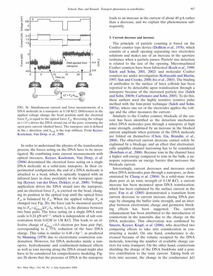
In order to understand the physics of the translocationprocess, the forces acting on the DNA have to be inves-tigated. By combining ionic current measurements withoptical tweezers, Keyser, Koeleman, Van Dorp, et al.�2006� determined the electrical force acting on a singleDNA molecule in a solid-state nanopore. In their ex-perimental configuration, the end of a DNA molecule isattached to a bead, which is optically trapped with aninfrared laser in close proximity to the nanopore open-ing �Keyser, van der Does, Dekker, et al., 2006�. Voltageapplication drives the DNA strand into the nanopore,and an electrical force Fel is exerted on the bead, chang-ing its position in the optical trap until the optical forceFot is balanced by Fel. When the applied voltage Va ischanged �see Fig. 26�, the force can be measured accord-ing to Fel=qDNA
* �Va / lb, where lb is the distance betweentwo base pairs. The force acting on a single DNA mol-ecule is 0.24 pN mV−1, which is independent of salt con-centration from 0.02M to 1M KCl. This leads to an ef-fective charge of qDNA
* =0.5 electron per base pair �bp�,corresponding to a 75% reduction of the bare DNAcharge. This value is similar to 0.48 e bp−1, as predictedby Manning �1978� due to electrostatic counterion con-densation. However, for DNA molecules inside a nan-opore, hydrodynamic and confinement-induced effectsas well as ions moving along the DNA strand might alsohave to be considered for comprehensive modeling. Fig-ure 26 shows that the presence of DNA in the nanopore
leads to an increase in the current of about 40 pA ratherthan a decrease, and we explain this phenomenon sub-sequently.
3. Current decrease and increase
The principle of particle counting is based on theCoulter counter type device �DeBlois et al., 1976�, whichconsists of a small opening separating two electrolytesolutions and makes use of an increase in the apertureresistance when a particle passes. Particle size detectionis related to the size of the opening. MicromachinedCoulter counters have been fabricated �Koch et al., 1999;Saleh and Sohn, 2001, 2002� and molecular Coultercounters are under investigation �Kobayashi and Martin,1997; Sun and Crooks, 2000; Ito et al., 2003�. The bindingof antibodies to the surface of latex colloids has beenreported to be detectable upon translocation through ananopore because of the increased particle size �Salehand Sohn, 2003b; Carbonaro and Sohn, 2005�. To do this,these authors used the highly sensitive resistive pulsemethod with the four-point technique �Saleh and Sohn,2003a�, where one set of the electrodes applies the volt-age and the other measures the current.
Similarly to the Coulter counter, blockade of the cur-rent has been identified as the detection mechanismwhen DNA molecules pass through a nanopore at highionic strength, confirmed by an increase in the blockedcurrent amplitude when portions of the DNA moleculeare folded on themselves �Chen, Gu, Brandin, et al.,2004�. The observed current decrease cannot solely beexplained by a blockage, and an effect that electrostati-cally amplifies channel narrowing has to be considered�Bonthuis et al., 2006�. Because ions in the channel havea higher self-energy compared to ions in the bulk, a na-nopore represents an energy barrier that increases theblockade current.
Interestingly, current decreases and increases resultwhen DNA molecules pass through a nanopore, as dem-onstrated by Chang et al. �2004�. In a solid-state 4-nm-diam pore at an ionic strength of 0.1M KCl, a currentincrease has been measured upon DNA translocation,which has been explained by the surface current in thepore. Fan et al. �2005� demonstrated a transition fromcurrent decrease to current increase during DNA pas-sage by changing the buffer ionic strength, and an inter-play between electrostatic charge and geometric block-ing effects has been suggested. The currentenhancement has been attributed to the introduction ofcounterions in the nanotube due to the charge on theDNA molecules. This observation was confirmed bySmeets, Keyser, Krapf, et al. �2006�, who described twocompeting effects to take into consideration in con-structing a model. On one hand, conductance is de-creased because of the volume occupied by the DNAmolecule, lowering the number of available charge car-riers for ionic transport. On the other hand, counterionsshielding the charge of the DNA backbone add a posi-tive contribution to the ionic current. Taking both ef-fects into account, the change in the conductance �G
0 5 10 15 20 25
-20
0
2.01.51.0
-40
D
0
-0.4
-0.8
0
100
-100Voltage(mV)
Current(nA)
Force(pN)
Time (s)
DNA ejected fromnanopore
∆Z = Fel/ktrap
Z(μm
)
FIG. 26. Simultaneous current and force measurements of aDNA molecule in a nanopore at 0.1M KCl. Differences in theapplied voltage change the bead position until the electricalforce Fel is equal to the optical force Fot. Reversing the voltageat t=13 s drives the DNA strand out of the pore, returning theopen-pore current �dashed lines�. The nanopore axis is definedin the z direction, and ktrap is the trap stiffness. From Keyser,Koeleman, Van Dorp, et al., 2006.
867Schoch, Han, and Renaud: Transport phenomena in nanofluidics
Rev. Mod. Phys., Vol. 80, No. 3, July–September 2008

due to DNA molecule translocation in a KCl solution is�Schoch, 2006; Smeets, Keyser, Krapf, et al., 2006�
�G =nDNA
d�−�
4dDNA
2 ��K+ + �Cl−�nKCle
+ �K+* qDNAl
* � , �62�
where nDNA is the number of DNA molecules in thenanopore, dDNA is the diameter of the DNA strand, �
K+*
is the effective electrophoretic mobility of potassiumions moving along the DNA strand, and qDNAl
* is theeffective charge on the DNA molecule per unit length,which is assumed to be constant. Smeets, Keyser,Krapf, et al. �2006� calculated that �
K+* qDNAl
* =2.09
�10−17 m �−1, which implies a reduced number of elec-trons per base pair �Rabin and Tanaka, 2005�. The cross-over concentration �Fig. 27� is obtained when �G=0 inEq. �62�, and this parameter is independent of the nan-opore length d.
Current increase during DNA translocation through ananopore at low ionic strength has also been computed
using a multi-ion model that accounts for the polariza-tion of the EDL �Liu et al., 2007�, and these theoreticalpredictions are in qualitative agreement with experi-mental observations.
B. Nanowire sensors
Similar to nanopores, nanowires are one-dimensionalnanostructures that show detectable electrical changesupon interactions with molecules. Such unique proper-ties are possible because the interactions have an effecton a significant part of the nanopore or nanowire, whichis related to their large surface-to-volume ratio. Thereader may perceive that nanowires have electrical ef-fects similar to those of previously described nanochan-nels. Such nanometer-scale phenomena have been ex-ploited to demonstrate sensitive, label-free, and real-time electrical detection with the integration ofnanowires in �TAS, which has high potential for use inhealth care, medicine, and life sciences, and has beendescribed in recent reviews �Lieber, 2003; Ramachan-dran et al., 2005; Gooding, 2006; Patolsky et al., 2006a,2006b; Carlen and Van den Berg, 2007�. However, thereasons for fast biomolecule detection at low analyteconcentrations are not yet understood, as described inSec. V.B.4, and further research in nanofluidics is neces-sary to explain such observations.
Carbon nanotubes have remarkable electrical proper-ties �Tans et al., 1998; Dekker, 1999� and can be used aselectrochemical sensors in liquids �Wang, 2005; Vam-vakaki et al., 2006; Zhou et al., 2007�. It has naturallybeen assumed that the observed conductance change isdue to the doping of the nanotube by adsorption of mol-ecules on its surface �Collins et al., 2000; Chen et al.,2003; Star et al., 2006�. However, Heinze et al. �2002�demonstrated that carbon nanotubes operate as uncon-ventional Schottky barrier transistors, in which switchingoccurs primarily by modulation of the contact resistancerather than channel conductance; this has been con-firmed by biomolecule detection studies �Chen, Choi,Bangsaruntip, et al., 2004; Tang et al., 2006�. Thus, thecontact resistance of the nanotube-electrode interfacemainly �unintentionally� determines the device opera-tion. In contrast, semiconductor nanowires interfacedwith low-bias ballistic contacts behave as preferentialfield-effect transistors. Additionally, applications ofhigh-performance nanotubes have been hindered by dif-ficulties in producing uniform semiconducting nano-tubes, a consideration that is not limited to nanowires.
1. Fabrication techniques
Nanowires can be fabricated using both “top-down”and “bottom-up” methods, but the latter techniques areless well suited for bulk production, which would hinderwidespread application of the technology. In order torealize fully integrated detection systems, the fabricationof nanowires with top-down methods is preferential andhas been considered to build complementary metal-oxide-semiconductor compatible nanowires with high
(a)
(b)
FIG. 27. Transition from current increase to current decreasefor DNA translocations through a nanopore. �a� Conductancechanges �G and �b� relative conductance changes �G /G dueto DNA molecule translocation for KCl concentrations be-tween 50 mM and 1M. Each symbol represents an individualpore, and the line is a linear fit to the data. The line in �b� hasbeen calculated for a change in surface charge as a function ofthe salt concentration. The inset shows the DNA moleculetranslocation time as a function of KCl concentration. FromSmeets, Keyser, Krapf, et al., 2006.
868 Schoch, Han, and Renaud: Transport phenomena in nanofluidics
Rev. Mod. Phys., Vol. 80, No. 3, July–September 2008
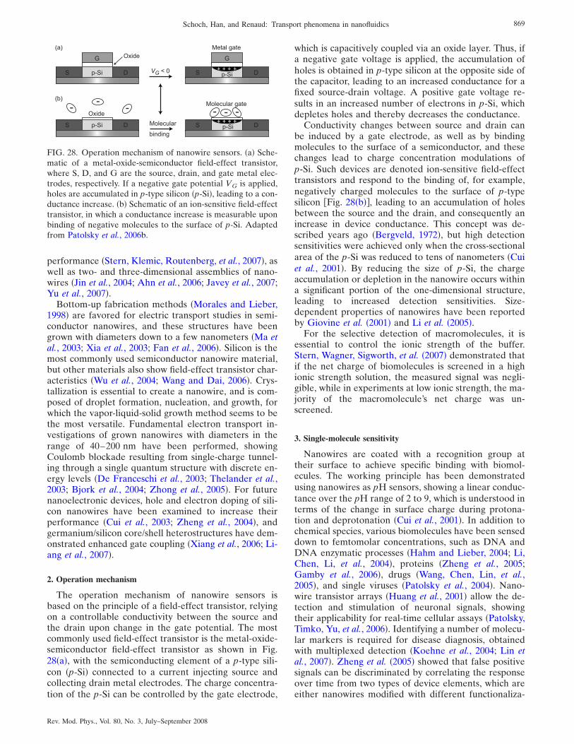
performance �Stern, Klemic, Routenberg, et al., 2007�, aswell as two- and three-dimensional assemblies of nano-wires �Jin et al., 2004; Ahn et al., 2006; Javey et al., 2007;Yu et al., 2007�.
Bottom-up fabrication methods �Morales and Lieber,1998� are favored for electric transport studies in semi-conductor nanowires, and these structures have beengrown with diameters down to a few nanometers �Ma etal., 2003; Xia et al., 2003; Fan et al., 2006�. Silicon is themost commonly used semiconductor nanowire material,but other materials also show field-effect transistor char-acteristics �Wu et al., 2004; Wang and Dai, 2006�. Crys-tallization is essential to create a nanowire, and is com-posed of droplet formation, nucleation, and growth, forwhich the vapor-liquid-solid growth method seems to bethe most versatile. Fundamental electron transport in-vestigations of grown nanowires with diameters in therange of 40–200 nm have been performed, showingCoulomb blockade resulting from single-charge tunnel-ing through a single quantum structure with discrete en-ergy levels �De Franceschi et al., 2003; Thelander et al.,2003; Bjork et al., 2004; Zhong et al., 2005�. For futurenanoelectronic devices, hole and electron doping of sili-con nanowires have been examined to increase theirperformance �Cui et al., 2003; Zheng et al., 2004�, andgermanium/silicon core/shell heterostructures have dem-onstrated enhanced gate coupling �Xiang et al., 2006; Li-ang et al., 2007�.
2. Operation mechanism
The operation mechanism of nanowire sensors isbased on the principle of a field-effect transistor, relyingon a controllable conductivity between the source andthe drain upon change in the gate potential. The mostcommonly used field-effect transistor is the metal-oxide-semiconductor field-effect transistor as shown in Fig.28�a�, with the semiconducting element of a p-type sili-con �p-Si� connected to a current injecting source andcollecting drain metal electrodes. The charge concentra-tion of the p-Si can be controlled by the gate electrode,
which is capacitively coupled via an oxide layer. Thus, ifa negative gate voltage is applied, the accumulation ofholes is obtained in p-type silicon at the opposite side ofthe capacitor, leading to an increased conductance for afixed source-drain voltage. A positive gate voltage re-sults in an increased number of electrons in p-Si, whichdepletes holes and thereby decreases the conductance.
Conductivity changes between source and drain canbe induced by a gate electrode, as well as by bindingmolecules to the surface of a semiconductor, and thesechanges lead to charge concentration modulations ofp-Si. Such devices are denoted ion-sensitive field-effecttransistors and respond to the binding of, for example,negatively charged molecules to the surface of p-typesilicon �Fig. 28�b��, leading to an accumulation of holesbetween the source and the drain, and consequently anincrease in device conductance. This concept was de-scribed years ago �Bergveld, 1972�, but high detectionsensitivities were achieved only when the cross-sectionalarea of the p-Si was reduced to tens of nanometers �Cuiet al., 2001�. By reducing the size of p-Si, the chargeaccumulation or depletion in the nanowire occurs withina significant portion of the one-dimensional structure,leading to increased detection sensitivities. Size-dependent properties of nanowires have been reportedby Giovine et al. �2001� and Li et al. �2005�.
For the selective detection of macromolecules, it isessential to control the ionic strength of the buffer.Stern, Wagner, Sigworth, et al. �2007� demonstrated thatif the net charge of biomolecules is screened in a highionic strength solution, the measured signal was negli-gible, while in experiments at low ionic strength, the ma-jority of the macromolecule’s net charge was un-screened.
3. Single-molecule sensitivity
Nanowires are coated with a recognition group attheir surface to achieve specific binding with biomol-ecules. The working principle has been demonstratedusing nanowires as pH sensors, showing a linear conduc-tance over the pH range of 2 to 9, which is understood interms of the change in surface charge during protona-tion and deprotonation �Cui et al., 2001�. In addition tochemical species, various biomolecules have been senseddown to femtomolar concentrations, such as DNA andDNA enzymatic processes �Hahm and Lieber, 2004; Li,Chen, Li, et al., 2004�, proteins �Zheng et al., 2005;Gamby et al., 2006�, drugs �Wang, Chen, Lin, et al.,2005�, and single viruses �Patolsky et al., 2004�. Nano-wire transistor arrays �Huang et al., 2001� allow the de-tection and stimulation of neuronal signals, showingtheir applicability for real-time cellular assays �Patolsky,Timko, Yu, et al., 2006�. Identifying a number of molecu-lar markers is required for disease diagnosis, obtainedwith multiplexed detection �Koehne et al., 2004; Lin etal., 2007�. Zheng et al. �2005� showed that false positivesignals can be discriminated by correlating the responseover time from two types of device elements, which areeither nanowires modified with different functionaliza-
S Dp-Si
G
VG < 0
S Dp-Si Molecular
binding
Metal gate
Molecular gate- - -
(a)
(b)
Oxide
Oxide -- -
+ +++
+ +++
S Dp-Si
G
S Dp-Si
FIG. 28. Operation mechanism of nanowire sensors. �a� Sche-matic of a metal-oxide-semiconductor field-effect transistor,where S, D, and G are the source, drain, and gate metal elec-trodes, respectively. If a negative gate potential VG is applied,holes are accumulated in p-type silicon �p-Si�, leading to a con-ductance increase. �b� Schematic of an ion-sensitive field-effecttransistor, in which a conductance increase is measurable uponbinding of negative molecules to the surface of p-Si. Adaptedfrom Patolsky et al., 2006b.
869Schoch, Han, and Renaud: Transport phenomena in nanofluidics
Rev. Mod. Phys., Vol. 80, No. 3, July–September 2008
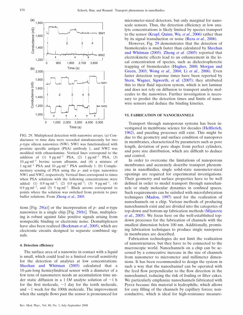
tions �Fig. 29�a�� or the incorporation of p- and n-typenanowires in a single chip �Fig. 29�b��. Thus, multiplex-ing is robust against false positive signals arising fromnonspecific binding or electronic noise. Demultiplexershave also been realized �Beckman et al., 2005�, which areelectronic circuits designed to separate combined sig-nals.
4. Detection efficiency
The surface area of a nanowire in contact with a liquidis small, which could lead to a limited overall sensitivityfor the detection of analytes at low concentrations.Sheehan and Whitman �2005� calculated that a10-�m-long hemicylindrical sensor with a diameter of afew tens of nanometers needs an accumulation time un-der static diffusion in a 1 fM analyte solution of �1 hfor the first molecule, �1 day for the tenth molecule,and �1 week for the 100th molecule. The improvementwhen the sample flows past the sensor is pronounced for
micrometer-sized detectors, but only marginal for nano-scale sensors. Thus, the detection efficiency at low ana-lyte concentrations is likely limited by species transportto the sensor �Krapf, Quinn, Wu, et al., 2006� rather thanby its signal transduction or noise �Reza et al., 2006�.
However, Fig. 29 demonstrates that the detection ofbiomolecules is much faster than calculated by Sheehanand Whitman �2005�. Zheng et al. �2005� reported thatelectrokinetic effects lead to an enhancement in the lo-cal concentration of species, such as dielectrophoretictrapping of biomolecules �Hughes, 2000; Morgan andGreen, 2003; Wong et al., 2004; Li et al., 2006�. Evenfaster detection response times have been reported byStern, Wagner, Sigworth, et al. �2007�; they attributedthis to their fluid injection system, which is not laminarand does not rely on diffusion to transport analyte mol-ecules to the nanowires. Further investigation is neces-sary to predict the detection times and limits of nano-wire sensors and deduce the binding kinetics.
VI. FABRICATION OF NANOCHANNELS
Transport through nanoporous systems has been in-vestigated in membrane science for decades �Helfferich,1962�, and puzzling processes still exist. This might bedue to the geometry and surface condition of nanoporesin membranes, characterized by parameters such as porelength, deviation of pore shape from perfect cylinders,and pore size distribution, which are difficult to deduceand control.
In order to overcome the limitations of nanoporousmembranes and accurately describe transport phenom-ena in nanofluidics, single solid-state nanometer-sizedopenings are required for experimental investigations.Their geometry and surface properties have to be welldefined in order to model transport through nanochan-nels or study molecular dynamics in confined spaces.Such requirements can be satisfied with microfabricationtechniques �Madou, 1997� used for the realization ofnanochannels on a chip. Various methods of producingnanochannels exist and are divided into the categories oftop-down and bottom-up fabrication methods �Mijatovicet al., 2005�. We focus here on the well-established top-down processes for the fabrication of channels with thesmallest dimension below 100 nm. Additionally, promis-ing fabrication techniques to produce single nanoporesin membranes are described.
Fabrication technologies do not limit the realizationof nanostructures, but they have to be connected to themacroscopic world. Nanochannels on a chip can be ac-cessed by a consecutive increase in the size of channelsfrom nanometer to micrometer and millimeter dimen-sions. It has been recommended to design the system insuch a way that the nanochannel can be operated withthe feed flow perpendicular to the flow direction in thenanochannel, reducing the risk of fouling or filter cakes.We particularly emphasize nanochannels fabricated withPyrex because this material is hydrophilic, which allowsfor easy filling of the channels by capillary forces; non-conductive, which is ideal for high-resistance measure-
(a)
(b)
FIG. 29. Multiplexed detection with nanowire arrays. �a� Con-ductance vs time data were recorded simultaneously for twop-type silicon nanowires �NW�. NW1 was functionalized withprostate specific antigen �PSA� antibody 1, and NW2 wasmodified with ethanolamine. Vertical lines correspond to theaddition of �1� 9 pg ml−1 PSA, �2� 1 pg ml−1 PSA, �3�10 �g ml−1 bovine serum albumin, and �4� a mixture of1 ng ml−1 PSA and 10 �g ml−1 PSA antibody 1. �b� Comple-mentary sensing of PSA using the p- and n-type nanowiresNW1 and NW2, respectively. Vertical lines correspond to timeswhen PSA solutions with the following concentrations wereadded: �1� 0.9 ng ml−1; �2� 0.9 ng ml−1; �3� 9 pg ml−1, �4�0.9 pg ml−1, and �5� 5 ng ml−1. Black arrows correspond topoints where the solution was switched from protein to purebuffer solutions. From Zheng et al., 2005.
870 Schoch, Han, and Renaud: Transport phenomena in nanofluidics
Rev. Mod. Phys., Vol. 80, No. 3, July–September 2008
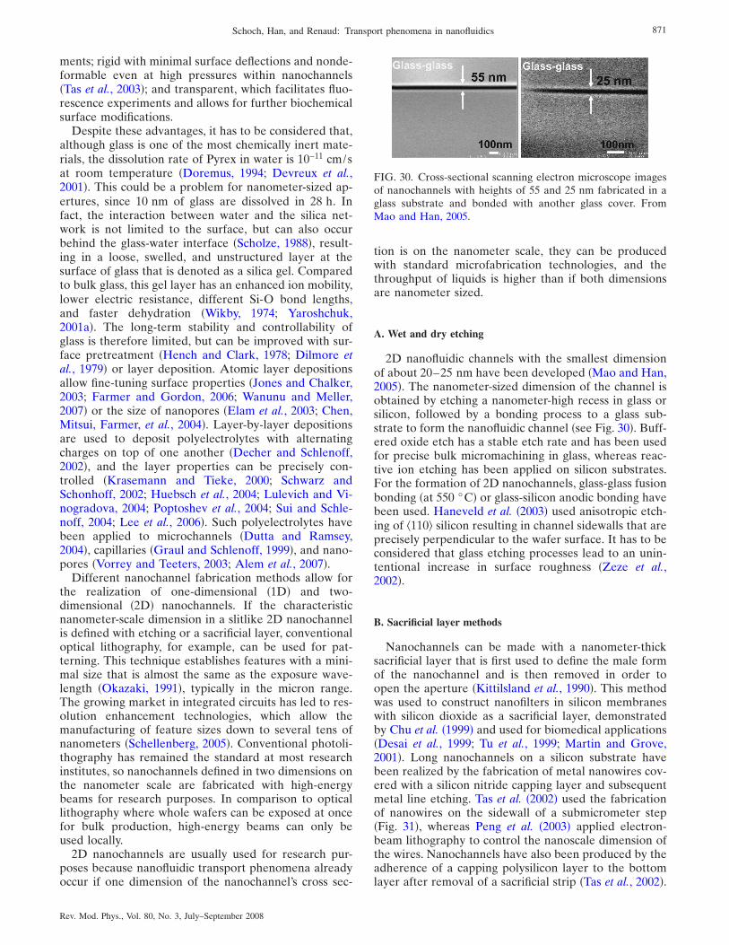
ments; rigid with minimal surface deflections and nonde-formable even at high pressures within nanochannels�Tas et al., 2003�; and transparent, which facilitates fluo-rescence experiments and allows for further biochemicalsurface modifications.
Despite these advantages, it has to be considered that,although glass is one of the most chemically inert mate-rials, the dissolution rate of Pyrex in water is 10−11 cm/sat room temperature �Doremus, 1994; Devreux et al.,2001�. This could be a problem for nanometer-sized ap-ertures, since 10 nm of glass are dissolved in 28 h. Infact, the interaction between water and the silica net-work is not limited to the surface, but can also occurbehind the glass-water interface �Scholze, 1988�, result-ing in a loose, swelled, and unstructured layer at thesurface of glass that is denoted as a silica gel. Comparedto bulk glass, this gel layer has an enhanced ion mobility,lower electric resistance, different Si-O bond lengths,and faster dehydration �Wikby, 1974; Yaroshchuk,2001a�. The long-term stability and controllability ofglass is therefore limited, but can be improved with sur-face pretreatment �Hench and Clark, 1978; Dilmore etal., 1979� or layer deposition. Atomic layer depositionsallow fine-tuning surface properties �Jones and Chalker,2003; Farmer and Gordon, 2006; Wanunu and Meller,2007� or the size of nanopores �Elam et al., 2003; Chen,Mitsui, Farmer, et al., 2004�. Layer-by-layer depositionsare used to deposit polyelectrolytes with alternatingcharges on top of one another �Decher and Schlenoff,2002�, and the layer properties can be precisely con-trolled �Krasemann and Tieke, 2000; Schwarz andSchonhoff, 2002; Huebsch et al., 2004; Lulevich and Vi-nogradova, 2004; Poptoshev et al., 2004; Sui and Schle-noff, 2004; Lee et al., 2006�. Such polyelectrolytes havebeen applied to microchannels �Dutta and Ramsey,2004�, capillaries �Graul and Schlenoff, 1999�, and nano-pores �Vorrey and Teeters, 2003; Alem et al., 2007�.
Different nanochannel fabrication methods allow forthe realization of one-dimensional �1D� and two-dimensional �2D� nanochannels. If the characteristicnanometer-scale dimension in a slitlike 2D nanochannelis defined with etching or a sacrificial layer, conventionaloptical lithography, for example, can be used for pat-terning. This technique establishes features with a mini-mal size that is almost the same as the exposure wave-length �Okazaki, 1991�, typically in the micron range.The growing market in integrated circuits has led to res-olution enhancement technologies, which allow themanufacturing of feature sizes down to several tens ofnanometers �Schellenberg, 2005�. Conventional photoli-thography has remained the standard at most researchinstitutes, so nanochannels defined in two dimensions onthe nanometer scale are fabricated with high-energybeams for research purposes. In comparison to opticallithography where whole wafers can be exposed at oncefor bulk production, high-energy beams can only beused locally.
2D nanochannels are usually used for research pur-poses because nanofluidic transport phenomena alreadyoccur if one dimension of the nanochannel’s cross sec-
tion is on the nanometer scale, they can be producedwith standard microfabrication technologies, and thethroughput of liquids is higher than if both dimensionsare nanometer sized.
A. Wet and dry etching
2D nanofluidic channels with the smallest dimensionof about 20–25 nm have been developed �Mao and Han,2005�. The nanometer-sized dimension of the channel isobtained by etching a nanometer-high recess in glass orsilicon, followed by a bonding process to a glass sub-strate to form the nanofluidic channel �see Fig. 30�. Buff-ered oxide etch has a stable etch rate and has been usedfor precise bulk micromachining in glass, whereas reac-tive ion etching has been applied on silicon substrates.For the formation of 2D nanochannels, glass-glass fusionbonding �at 550 °C� or glass-silicon anodic bonding havebeen used. Haneveld et al. �2003� used anisotropic etch-ing of �110� silicon resulting in channel sidewalls that areprecisely perpendicular to the wafer surface. It has to beconsidered that glass etching processes lead to an unin-tentional increase in surface roughness �Zeze et al.,2002�.
B. Sacrificial layer methods
Nanochannels can be made with a nanometer-thicksacrificial layer that is first used to define the male formof the nanochannel and is then removed in order toopen the aperture �Kittilsland et al., 1990�. This methodwas used to construct nanofilters in silicon membraneswith silicon dioxide as a sacrificial layer, demonstratedby Chu et al. �1999� and used for biomedical applications�Desai et al., 1999; Tu et al., 1999; Martin and Grove,2001�. Long nanochannels on a silicon substrate havebeen realized by the fabrication of metal nanowires cov-ered with a silicon nitride capping layer and subsequentmetal line etching. Tas et al. �2002� used the fabricationof nanowires on the sidewall of a submicrometer step�Fig. 31�, whereas Peng et al. �2003� applied electron-beam lithography to control the nanoscale dimension ofthe wires. Nanochannels have also been produced by theadherence of a capping polysilicon layer to the bottomlayer after removal of a sacrificial strip �Tas et al., 2002�.
FIG. 30. Cross-sectional scanning electron microscope imagesof nanochannels with heights of 55 and 25 nm fabricated in aglass substrate and bonded with another glass cover. FromMao and Han, 2005.
871Schoch, Han, and Renaud: Transport phenomena in nanofluidics
Rev. Mod. Phys., Vol. 80, No. 3, July–September 2008

Centimeter-long nanochannels can be fabricated with asacrificial SiO2 layer �Lee et al., 2003; Han, de Rooij, andStaufer, 2006�.
Sacrificial layers can be used as nanometer-sized spac-ers between two substrates to define their separationdistance. For example, by patterning a layer of amor-phous silicon with photolithography, 2D nanochannelswith heights of 50 nm have been realized in Pyrex�Schoch et al., 2005�. This method allows convenientcontact of the nanochannel with two microchannels,which are fabricated by wet etching �Fig. 32�.
C. High-energy beam techniques
The focused ion beam is a powerful tool used to di-rectly fabricate structures on the substrate down to sometens of nanometers. This instrument has been used tomill or etch 1D nanochannels in different types of mate-rials such as glass �Wang, Tegenfeldt, Reisner, et al.,2005; Schoch, 2006�, silicon �Campbell et al., 2004�, andpoly�methyl methacrylate� �Cannon et al., 2004�.
In electron-beam lithography, the pattern is directlyexposed to the resist �or ice layer �King et al., 2005�� onthe substrate, and structures are then obtained with bulkmicromachining. For example, this technique has beenused to produce monolithic nanofluidic sieving struc-tures that are similar to two-dimensional artificial gelsused for DNA molecule manipulations �Volkmuth andAustin, 1992; Turner et al., 1998�. These structures arealso useful for interfacing microfluidic and nanofluidicchannels �Cao et al., 2002�. An asymmetric lattice of or-thogonally interconnected nanochannels with equalpitch and dissimilar channel cross section has been fab-ricated using electron-beam lithography by Riehn et al.�2006�, which could be used for the separation of DNAmolecules �Sec. IV.D�.
D. Nanoimprint lithography
A low-cost and high-throughput method for the fabri-cation of 2D nanofluidic channels is nanoimprint lithog-raphy, which was first reported by Chou and Krauss�1997�. In a single step with elevated temperature andpressure, a channel template can be imprinted onto athin polymer film cast on a glass cover slip �Quake andScherer, 2000; Guo et al., 2003; Cheng and Guo, 2004� oronto a poly�methyl methacrylate� wafer �Abgrall et al.,2007�. The nanochannel dimensions are controlled by asimple relationship involving the initial polymer layerthickness and the mold pattern configuration, and thegrating period can be reduced by frequency doubling�Cui et al., 2007�. Nanoimprint lithography has also beendemonstrated on free-standing membranes �Heydermanet al., 2003�.
E. Bonding and sealing methods
To achieve encapsulation of bulk-machinednanochannels, bonding and sealing has to be performed.Depending on the bulk material in which the nanochan-nels have been produced �Madou, 1997�, different meth-ods can be used. Two silicon wafers can be joined bysilicon fusion bonding at temperatures above 1000 °C.For the fabrication of silicon-on-glass wafers, anodicbonding is known to result in high bonding strengthwhen simultaneously exposing the wafers to an elevated-temperature treatment of about 500 °C and a dc voltageof approximately 750 V �Knowles and van Helvoort,2006�. Methods for bonding between two glass waferscan be divided into methods using either high tempera-ture �glass fusion bonding�, extremely high pressures�Sayah et al., 2000�, or chemicals such as hydrofluoricacid �Nakanishi et al., 2000; Chen et al., 2006�. Fabrica-tion processes at lower temperatures have been devel-oped because high temperatures are not suitable forheat-sensitive materials such as electrodes.
Glass wafers with an intermediate layer of amorphoussilicon can be bonded at temperatures of about 250 °Cand a dc voltage of approximately 500 V �Berthold et al.,2000; Lee et al., 2001�. This field-assisted bonding tech-nique is interesting for microelectronic devices, since en-capsulation is achieved at reasonable temperatures.Other intermediate or adhesive layers �Niklaus et al.,2006� have been used for wafer bonding, such as waterglass �Satoh, 1999; Ito et al., 2002�, spin-on glass �Wang etal., 1997�, benzocyclobutene �Niklaus et al., 2001�, orglue �Sayah et al., 2000�. However, using such adhesivelayers for the fabrication of nanochannels bears the riskof nanochannel clogging.
F. Realization of single nanopores in membranes
The realization of single nanopores fabricated in amembrane are not the principal focus of this review, butwe present selected techniques in this area. The integra-tion capabilities of membranes in �TAS are growing
(a) (b)
200 nm150 nm
FIG. 31. Scanning electron microscope images of 2D definednanochannels fabricated by two different sacrificial layer meth-ods. �a� Formation of a nanowire on the sidewall of a step and�b� etching of a sacrificial strip separating the substrate and thecapping layer. From Tas et al., 2002.
50 nmPyrex
Pyrex
aSi
50 nm
100 nm
FIG. 32. Cross section of a chip illustrating two microchannelslinked by a nanochannel, whose height is defined by the thick-ness of the amorphous silicon �a-Si� layer. The inset shows ascanning electron microscope image of the 50-nm-highnanochannel. Adapted from Schoch, 2006.
872 Schoch, Han, and Renaud: Transport phenomena in nanofluidics
Rev. Mod. Phys., Vol. 80, No. 3, July–September 2008

�Kuo et al., 2003; de Jong et al., 2006; Flachsbart et al.,2006�, and solid membranes produced in a wafer seem tobe the most suitable for this.
The smallest single nanopore that can be achieved in asolid is fabricated with high-energy beams, and is prom-ising for DNA translocation measurements as presentedin Sec. IV. For its fabrication, a 60-nm-diam pore wasmade with a focused ion beam on a 500-nm-thick siliconnitride membrane. Li et al. �2001� exposed this pore to a3 keV Ar+ ion beam, which decreased the initial poresize of 60 nm down to 1.8 nm �Fig. 33�. In this method,called “ion beam sculpting,” the atomic flow of matterinto the pore occurs upon stimulation by the ion beam.Storm et al. �2003� used a transmission electron micro-scope to shrink a pore. First, a 20 nm pore was fabri-cated in a 350-nm-thick silicon membrane usingelectron-beam lithography and anisotropic etching. Af-ter thermal oxidation, the pore was reduced to 2 nm,since the silicon oxide can be fluidized upon exposure toa high-energy electron-beam. It is proposed that Joule-heating-assisted irradiation-induced diffusion is the rea-son for such shrinkage �Zhang et al., 2007�.
A different technique can be used to produce syn-thetic nanopores with diameters of 1.8 nm in 10-nm-thick membranes, and is based on drilling �Storm et al.,2003; Ho et al., 2005�. Single nanopores in a variety ofmembrane materials have been achieved with electron-beam-stimulated decomposition and sputtering using atransmission electron microscope operated at200–300 keV, which generates a tightly focused beam assmall as 0.5 nm in diameter. Such pores in silicon nitridehave been reduced in size by Krapf, Wu, Smeets, et al.�2006� upon exposure to a low-intensity electron beam,allowing shrinkage down to a 0.8-nm-diam opening, rep-resenting the smallest reported nanopore. Monolayerdeposition of silicon oxide to shrink an initial 50-nm-diam pore down to 4 nm in a silicon nitride membranewas demonstrated by Danelon et al. �2006�. These poresare suitable for further biochemical surface modifica-tions.
Single and asymmetric nanopores with diametersdown to 2 nm can be fabricated in a polymer foil usingthe track etching technique, based on the irradiation of apolymer foil with energetic heavy ions and subsequentchemical etching �Siwy and Fulinski, 2002a; Harrell et
al., 2003; Siwy, Apel, Dobrev, et al., 2003; Li, Harrell,and Martin, 2004�. Fast heavy ions can lead to perma-nent material changes along the nearly straight ion path,referred to as ion tracks, which can be selectivelyopened with appropriate etchants. Asymmetric poreshave been shown to exhibit unique properties, specifi-cally asymmetric diffusion �Siwy, Kosinska, Fulinski, etal., 2005�, ionic current rectification �see Sec. III.A.3��Wei et al., 1997; Siwy et al., 2004; Cervera et al., 2006;Vlassiouk and Siwy, 2007� by using calcium �Siwy et al.,2006� or DNA �Harrell et al., 2004� to change the surfaceproperties, voltage gating similar to biological channels�Siwy, Apel, Baur, et al., 2002, 2003�, and sensing of pro-teins �Siwy, Trofin, Kohli, et al., 2005�.
More recently, multiple nanopores with controlledsizes between 5 and 25 nm were fabricated in a 15-nm-thick nanocrystalline silicon membrane, which has re-markable mechanical properties �Striemer et al., 2007�.Nanopores are obtained from voids formed spontane-ously as nanocrystals of the membrane nucleate andgrow during rapid thermal annealing. Currently, thisprocess cannot be predicted with existing models.
VII. CONCLUSIONS AND PERSPECTIVES
This review shows that nanofluidics offers a variety ofunique properties in nanochannels, nanofilters, nanop-ores, nanowires, and at the microchannel-nanochannelinterface. In such nanostructures, transport phenomenathat are accessible only at these length scales can beachieved, and this opens new opportunities and researchdirections. Thus, nanofluidics is significantly relevant tonanoscience and nanotechnology, and may lead to newadvances.
The nanostructures presented have been kept rela-tively simple in order to elucidate their physical prin-ciples, establishing a basis for massive parallelism withintegrated electrical characterizations for potential na-noelectrofluidic systems. Such devices have a high po-tential for impact in biological and medical applicationsfor separation, detection, and analytic purposes. Nano-fluidic systems have the capability of dealing with a lim-ited amount of sample, which is particularly important inbiomedicine, for example, to analyze species from asingle cell. Important practical significance is attributedto the substantial decrease in the immunoassay responsetime, demonstrated in nanochannels with an inducedflow �Schoch et al., 2007�.
In addition to the elucidated properties of nanofluidicsystems, chemical and physical properties of single mol-ecules can be investigated in nanochannels �Craighead,2006�. Such single-molecule interrogations have demon-strated restriction mapping of DNA molecules �Riehn etal., 2005� and repressor-DNA interactions �Wang,Tegenfeldt, Reisner, et al., 2005�. Dependent on the con-finement degree of DNA in nanochannels, diffusivity�Balducci et al., 2006� and stretching �Tegenfeldt, Prinz,Cao, Chou, et al., 2004; Reisner et al., 2005; Jo et al.,2007; Krishnan et al., 2007� have been studied at differ-ent conditions to describe the fundamental properties of
(a) (b)
FIG. 33. Transmission electron microscope image of �a� initial60-nm-diam pore and �b� the same sample after ion beam ex-posure yielding a shrunken 1.8-nm-diam pore. From Li et al.,2001.
873Schoch, Han, and Renaud: Transport phenomena in nanofluidics
Rev. Mod. Phys., Vol. 80, No. 3, July–September 2008

these polymer molecules. For single-molecule analysis,optical techniques are the most straightforward, stan-dard fluorescence microscopy is typically used, and fluo-rescence correlation spectroscopy �Magde et al., 1972;Hess et al., 2002� in submicrometer-sized channels �Fo-quet et al., 2002, 2004� and near-field scanners with highspatial resolution �Tegenfeldt et al., 2001; Tegenfeldt,Prinz, Cao, Huang, et al., 2004� are also considered.
ACKNOWLEDGMENTS
This review originates from the Ph.D. thesis of Schoch�2006� and his work as a Postdoctoral Associate, and wetherefore gratefully acknowledge support from the pro-gram “Doktorieren an der anderen ETH” and theDuPont-MIT Alliance.
LISTS OF ABBREVIATIONS AND SYMBOLSCPE constant phase elementDBL diffusion boundary layerEDL electrical double layerEEE exclusion-enrichment effect�TAS micro total analysis systemsA surface area m2
CCPE CPE capacitance FCGC Gouy-Chapman layer capacitance FCH Helmholtz layer capacitance FCstray stray capacitance FD diffusion coefficient m2 s−1
E electric field V m−1
Es electric field in nanochannel V m−1
Et tangential electric field V m−1
Fe entropic force kg m s−2
Fel electrical force kg m s−2
Fot optical force kg m s−2
G conductance SGp conductance plateau SI current AId current density A m−2
Id0exchange current density A m−2
Ilim limited current AIs ionic strength MJ, J flux per area mol s−1 m−2
KL bulk conductivity S m−1
K� surface conductance SK�d surface conductance of diffuse
layer SK�i surface conductance of Stern layer SL mean drift distance mN DNA base-pair numberP* geometrical permeability m3 s−1
Peff effective permeability m3 s−1
Px passage rate mol s−1
R0 radius of gyration mRnano resistance of nanochannel �Rt charge-transfer resistance �m−2
S* geometrical cross section m2
Seff effective cross section m2
T absolute temperature KV0 equilibrium potential VVa applied potential VZCPE impedance of CPE �ZW Warburg impedance �a grid size map particle radius mc, c concentration Mc* concentration at high Is Mc0 standard molarity of 1 Mcb bulk concentration Mce excess mobile counterion
concentration Mceff effective concentration Mct transition concentration Mcw wall charge concentration Md length of nanochannel mdDNA diameter of DNA strand mdOHP distance to outer Helmholtz plane mf friction coefficient kg s−1
fs specific friction coefficient kg m−1 s−1
h height of nanochannel mlb distance between base pairs mnCPE CPE exponentnDNA number of DNA in nanoporeni volume density m−3
ni� bulk volume density m−3
p pressure N m−2
q net charge eqDNA
* effective DNA q per base pair e bp−1
qDNAl
* effective DNA q per length C m−1
r radial coordinate mr0 radius of pore mrD Donnan ratiot time stan transference number of aniontca transference number of cationtd depth of deep region mts depth of shallow region mvc convective velocity field m s−1
veo electro-osmotic velocity m s−1
veo2 veo of the second kind m s−1
vep electrophoretic velocity m s−1
w width of nanochannel mx x direction mxf DNA length inside filter mxp DNA length inside pillar array my y direction mz z direction mzi valency of ion i� electric potential V�n applied electric potential V�D Donnan potential V�diff diffusion potential V�m membrane potential V�m molar conductivity S m2 mol−1
874 Schoch, Han, and Renaud: Transport phenomena in nanofluidics
Rev. Mod. Phys., Vol. 80, No. 3, July–September 2008
�m0 limiting molar conductivity S m2 mol−1
� constant� exclusion-enrichment coefficient�part partition coefficient! DBL thickness m� energy J�p potential energy Jr relative permittivity� flux mol s−1
�* geometrical flux mol s−1
�eff effective flux mol s−1
�bulk bulk conductivity S m−1
�a activity coefficient� dynamic viscosity kg m−1 s−1
� streaming potential V� Debye-Hückel parameter m−1
D Debye length m� mobility m2 V−1 s−1
�* effective mobility on DNA m2 V−1 s−1
�eo electro-osmotic mobility m2 V−1 s−1
�ep electrophoretic mobility m2 V−1 s−1
�̃ chemical potential J mol−1
�5 electrochemical potential J mol−1
# deflection angle deg� charge density C m−3
�d diffuse layer charge density C m−2
�s surface charge density C m−2
" trapping lifetime s"0 " at high electric field s� symmetry factor� frequency Hz� electric potential due to �s V�ct charge-transfer overpotential V�d diffuse layer potential V�i inner Helmholtz plane potential V�s surface potential V�to total overpotential V� zeta potential V
Fundamental constants and unitsF Faraday constant 96 485 C mol−1
NA Avogadro constant 6.022�1023 mol−1
R gas constant 8.314 J mol−1 K−1
e charge of the electron 1.602�10−19 CkB Boltzmann constant 1.381�10−23 J K−1
0 permittivity of freespace 8.854�10−12 F m−1
Capaci-tance farad F=C V−1=A2 s4 kg−1 m−2
Charge coulomb C=A sConcen-tration molar M=mol l−1=103 mol m−3
Energy joule J=N m=kg m2 s−2
Force newton N=kg m s−2
Frequency hertz Hz=s−1
Power watt W=J s−1=kg m2 s−3
Pressure pascal Pa=N m−2=kg m−1 s−2
Resistance
ohm �=V A−1=kg m2 A−2 s−3
Voltage volt V=J C−1=kg m2 A−1 s−3
REFERENCES
Abendrot, R. P., 1970, J. Colloid Interface Sci. 34, 591.Abgrall, P., L.-N. Low, and N.-T. Nguyen, 2007, Lab Chip 7,
520.Adamczyk, Z., M. Zembala, P. Warszynski, and B. Jachimska,
2004, Langmuir 20, 10517.Ahn, J.-H., H.-S. Kim, K. J. Lee, S. Jeon, S. J. Kang, Y. Sun, R.
G. Nuzzo, and J. A. Rogers, 2006, Science 314, 1754.Ajdari, A., and J. Prost, 1992, C. R. Acad. Sci., Ser. II: Mec.,
Phys., Chim., Sci. Terre Univers 315, 1635.Aksimentiev, A., J. B. Heng, G. Timp, and K. Schulten, 2004,
Biophys. J. 87, 2086.Alem, H., F. Blondeau, K. Glinel, S. Demoustier-Champagne,
and A. M. Jonas, 2007, Macromolecules 40, 3366.Alexov, E., 2004, Eur. J. Biochem. 271, 173.Anderson, N. L., and N. G. Anderson, 1998, Electrophoresis
19, 1853.Asbury, C. L., and G. v. d. Engh, 1998, Biophys. J. 74, 1024.Ashkenasy, N., J. Sanchez-Quesada, H. Bayley, and M. R.
Ghadiri, 2005, Angew. Chem., Int. Ed. 44, 1401.Austin, R. H., N. Darnton, R. Huang, J. Sturm, O. Bakajin,
and T. Duke, 2002, Appl. Phys. A: Mater. Sci. Process. 75,279.
Baldessari, F., and J. G. Santiago, 2006, J. Nanobiotechnol. 4,12.1.
Balducci, A., P. Mao, J. Han, and P. S. Doyle, 2006, Macromol-ecules 39, 6273.
Basu, S., and M. M. Sharma, 1997, J. Membr. Sci. 124, 77.Bates, M., M. Burns, and A. Meller, 2003, Biophys. J. 84, 2366.Bath, B., H. White, and E. Scott, 2000, Anal. Chem. 72, 433.Bayley, H., and P. S. Cremer, 2001, Nature 413, 226.Bazant, M. Z., K. Thornton, and A. Ajdari, 2004, Phys. Rev. E
70, 021506.Bean, C. P., M. V. Doyle, and G. Entine, 1970, J. Appl. Phys.
41, 1454.Beck, R. E., and J. S. Schultz, 1970, Science 170, 1302.Beckman, R., E. Johnston-Halperin, Y. Luo, J. E. Green, and
J. R. Heath, 2005, Science 310, 465.Beckstein, O., P. C. Biggin, P. Bond, J. N. Bright, C. Domene,
A. Grottesi, J. Holyoake, and M. S. Sansom, 2003, FEBSLett. 555, 85.
Behrens, S. H., and M. Borkovec, 1999, Phys. Rev. E 60, 7040.Behrens, S. H., and D. G. Grier, 2001, J. Chem. Phys. 115,
6716.Ben, Y., and H.-C. Chang, 2002, J. Fluid Mech. 461, 229.Bergveld, P., 1972, IEEE Trans. Biomed. Eng. 19, 342.Berthold, A., L. Nicola, P. M. Sarro, and M. J. Vellekoop, 2000,
Sens. Actuators, A 82, 224.Bezrukov, S. M., and M. Winterhalter, 2000, Phys. Rev. Lett.
85, 202.Bhatt, K., O. Velev, and S. Grego, 2005, Langmuir 21, 6603.Bhattacharjee, S., J. Chen, and M. Elimelech, 2001, AIChE J.
47, 2733.Bianchi, F., F. Wagner, P. Hoffmann, and H. H. Girault, 2001,
Anal. Chem. 73, 829.Bjork, M. T., C. Thelander, A. E. Hansen, L. E. Jensen, M. W.
Larsson, L. R. Wallenberg, and L. Samuelson, 2004, NanoLett. 4, 1621.
Bluhm, E. A., E. Bauer, R. M. Chamberlin, K. D. Abney, J. S.
875Schoch, Han, and Renaud: Transport phenomena in nanofluidics
Rev. Mod. Phys., Vol. 80, No. 3, July–September 2008
Young, and G. D. Jarvinen, 1999, Langmuir 15, 8668.Bockris, J. O., and A. K. N. Reddy, 2000, Modern Electro-
chemistry, 2nd ed. �Kluwer Academic, New York�, Vol. 2B.Bonthuis, D. J., J. Zhang, B. Hornblower, J. Mathe, B. I.
Shklovskii, and A. Meller, 2006, Phys. Rev. Lett. 97, 128104.Bostrom, M., F. Tavares, S. Finet, F. Skouri-Panet, A. Tardieu,
and B. Ninham, 2005, Biophys. Chem. 117, 217.Bourlon, B., J. Wong, C. Miko, L. Forro, and M. Bockrath,
2007, Nat. Nanotechnol. 2, 104.Bowen, R. W., W. A. Mohammad, and N. Hilal, 1997, J.
Membr. Sci. 126, 91.Bowen, W. R., and J. S. Welfoot, 2002, Chem. Eng. Sci. 57,
1121.Burgreen, D., and F. Nakache, 1964, J. Phys. Chem. 68, 1084.Burns, D., and A. Zydney, 1999, Biotechnol. Bioeng. 64, 27.Bushong, N., J. Gamble, and M. Di Ventra, 2007, Nano Lett. 7,
1789.Cabodi, M., Y.-F. Chen, S. W. Turner, H. G. Craighead, and R.
H. Austin, 2002, Electrophoresis 23, 3496.Cabodi, M., S. W. Turner, and H. G. Craighead, 2002, Anal.
Chem. 74, 5169.Campbell, L. C., M. J. Wilkinson, A. Manz, P. Camilleri, and C.
J. Humphreys, 2004, Lab Chip 4, 225.Cannon, D. M., B. R. Flachsbart, M. A. Shannon, J. V.
Sweedler, and P. W. Bohn, 2004, Appl. Phys. Lett. 85, 1241.Cannon, D. M., T.-C. Kuo, P. W. Bohn, and J. V. Sweedler,
2003, Anal. Chem. 75, 224.Cao, H., J. Tegenfeldt, R. Austin, and S. Y. Chou, 2002, Appl.
Phys. Lett. 81, 3058.Carbonaro, A., and L. L. Sohn, 2005, Lab Chip 5, 1155.Carlen, E. T., and A. Van den Berg, 2007, Lab Chip 7, 19.Cervera, J., A. Alcaraz, B. Schiedt, R. Neumann, and P.
Ramirez, 2007, J. Phys. Chem. C 111, 12265.Cervera, J., B. Schiedt, R. Neumann, S. Mafe, and P. Ramirez,
2006, J. Chem. Phys. 124, 104706.Cevc, G., 1990, Biochim. Biophys. Acta 1031, 311.Chan, E. Y., 2005, Mutat Res. 573, 13.Chang, H., F. Kosari, G. Andreadakis, M. A. Alam, G. Vas-
matzis, and R. Bashir, 2004, Nano Lett. 4, 1551.Chaufer, B., M. Rabiller-Baudry, L. Guihard, and G. Daufin,
1996, Desalination 104, 37.Chen, L., G. Luo, K. Liu, J. Ma, B. Yao, Y. Yan, and Y. Wang,
2006, Sens. Actuators B 119, 335.Chen, P., J. Gu, E. Brandin, Y.-R. Kim, Q. Wang, and D. Bran-
ton, 2004, Nano Lett. 4, 2293.Chen, P., T. Mitsui, D. B. Farmer, J. A. Golovchenko, R. G.
Gordon, and D. Branton, 2004, Nano Lett. 4, 1333.Chen, R. J., S. Bangsaruntip, K. A. Drouvalakis, N. W. S. Kam,
M. Shim, Y. M. Li, W. Kim, P. J. Utz, and H. J. Dai, 2003,Proc. Natl. Acad. Sci. U.S.A. 100, 4984.
Chen, R. J., H. C. Choi, S. Bangsaruntip, E. Yenilmez, X. W.Tang, Q. Wang, Y. L. Chang, and H. J. Dai, 2004, J. Am.Chem. Soc. 126, 1563.
Cheng, J. T., and N. Giordano, 2002, Phys. Rev. E 65, 031206.Cheng, L. J., and L. J. Guo, 2007, Nano Lett. 7, 3165.Cheng, X., and L. Guo, 2004, Microelectron. Eng. 71, 288.Chou, C.-F., R. H. Austin, O. Bakajin, J. O. Tegenfeldt, J. A.
Castelino, S. S. Chan, E. C. Cox, H. G. Craighead, N. Darn-ton, T. Duke, J. Han, and S. W. Turner, 2000, Electrophoresis21, 81.
Chou, C. F., O. Bakajin, S. W. P. Turner, T. A. J. Duke, S. S.Chan, E. C. Cox, H. G. Craighead, and R. H. Austin, 1999,Proc. Natl. Acad. Sci. U.S.A. 96, 13762.
Chou, S. Y., and P. R. Krauss, 1997, Microelectron. Eng. 35,237.
Chu, W.-H., R. Chin, T. Huen, and M. Ferrari, 1999, J. Micro-electromech. Syst. 8, 34.
Chun, K.-Y., S. Mafe, P. Ramirez, and P. Stroeve, 2006, Chem.Phys. Lett. 418, 557.
Chun, K. Y., and P. Stroeve, 2002, Langmuir 18, 4653.Collins, P. G., K. Bradley, M. Ishigami, and A. Zettl, 2000,
Science 287, 1801.Conlisk, A. T., 2005, Electrophoresis 26, 1896.Conlisk, A. T., J. McFerran, Z. Zheng, and D. Hansford, 2002,
Anal. Chem. 74, 2139.Corthals, G. L., M. P. Molloy, B. R. Herbert, K. L. Williams,
and A. A. Gooley, 1997, Electrophoresis 18, 317.Craig Venter, J., et al., 2001, Science 291, 1304.Craighead, H., 2006, Nature 442, 387.Craighead, H. G., 2003, J. Vac. Sci. Technol. A 21, S216.Cui, B., Z. Yu, H. Ge, and S. Y. Chou, 2007, Appl. Phys. Lett.
90, 043118.Cui, Y., Q. Q. Wei, H. K. Park, and C. M. Lieber, 2001, Science
293, 1289.Cui, Y., Z. H. Zhong, D. L. Wang, W. U. Wang, and C. M.
Lieber, 2003, Nano Lett. 3, 149.Cussler, E. L., 1997, Diffusion, Mass Transfer in Fluid Systems,
2nd ed. �Cambridge University, New York�.Daiguji, H., Y. Oka, and K. Shirono, 2005, Nano Lett. 5, 2274.Daiguji, H., P. Yang, and A. Majumdar, 2004, Nano Lett. 4,
137.Daiguji, H., P. Yang, A. J. Szeri, and A. Majumdar, 2004, Nano
Lett. 4, 2315.Danelon, C., C. Santschi, J. Brugger, and H. Vogel, 2006,
Langmuir 22, 10711.Davis, J. A., R. O. James, and J. O. Leckie, 1978, J. Colloid
Interface Sci. 63, 480.De Franceschi, S., J. A. van Dam, E. Bakkers, L. F. Feiner, L.
Gurevich, and L. P. Kouwenhoven, 2003, Appl. Phys. Lett. 83,344.
De Leebeeck, A., and D. Sinton, 2006, Electrophoresis 27,4999.
Deamer, D. W., and M. Akeson, 2000, Trends Biotechnol. 18,147.
DeBlois, R. W., C. P. Bean, and R. K. A. Wesley, 1976, J.Colloid Interface Sci. 61, 323.
Decher, G., and J. B. Schlenoff, 2002, Multilayer Thin Films�Wiley-VCH, Weinheim, Germany�.
Deen, W., 1987, AIChE J. 33, 1409.de Gennes, P., 1971, J. Chem. Phys. 55, 572.de Gennes, P., 1979, Scaling Concepts of Polymer Physics �Cor-
nell University Press, Ithaca, NY�.de Jong, J., R. G. H. Lammertink, and M. Wessling, 2006, Lab
Chip 6, 1125.Dekker, C., 1999, Phys. Today 52 �5�, 22.Dekker, C., 2007, Nat. Nanotechnol. 2, 209.Delft, K. M. v., J. C. T. Eijkel, D. Mijatovic, T. S. Druzhinina,
H. Rathgen, N. R. Tas, A. v. d. Berg, and F. Mugele, 2007,Nano Lett. 7, 345.
DeRosa, J. F., and R. B. Beard, 1977, IEEE Trans. Biomed.Eng. 24, 260.
Desai, T., D. Hansford, L. Kulinsky, A. Nashat, G. Rasi, J. Tu,Y. Wang, M. Zhang, and M. Ferrari, 1999, Biomed. Microde-vices 2, 11.
Devreux, F., P. Barboux, M. Filoche, and B. Sapoval, 2001, J.Mater. Sci. 36, 1331.
876 Schoch, Han, and Renaud: Transport phenomena in nanofluidics
Rev. Mod. Phys., Vol. 80, No. 3, July–September 2008
Di Ventra, M., S. Evoy, and J. R. Heflin, 2004, Introduction toNanoscale Science and Technology, Nanostructure Scienceand Technology �Kluwer Academic, Boston�.
Dilmore, M. F., D. E. Clark, and L. L. Hench, 1979, Ceram.Bull. 58, 1111.
Dittrich, P. S., K. Tachikawa, and A. Manz, 2006, Anal. Chem.78, 3887.
Donnan, F. G., 1924, Chem. Rev. �Washington, D.C.� 1, 73.Donnan, F. G., 1995, J. Membr. Sci. 100, 45.Doremus, R. H., 1994, Glass Science, 2nd ed. �Wiley, New
York�.Doyle, D., R. Pfuetzner, A. Kuo, R. MacKinnon, J. Cabral, J.
Gulbis, S. Cohen, and B. Chait, 1998, Science 89, 244501.Drazer, G., J. Koplik, A. Acrivos, and B. Khusid, 2002, Phys.
Rev. Lett. 89, 244501.Duke, T., and R. Austin, 1998, Phys. Rev. Lett. 80, 1552.Dukhin, S. S., 1991, Adv. Colloid Interface Sci. 35, 173.Dukhin, S. S., and V. Shilov, 1969, Colloid J. USSR 31, 564.Duong-Hong, D., J.-S. Wang, G. R. Liu, Y. Z. Chen, J. Han,
and G. Hadjiconstantinou, Nicolas, 2007, Microfluid. Nano-fluid. 4, 219.
Dutta, D., and J. M. Ramsey, 2004, in Proceedings of Micro-TAS, edited by T. Laurell, J. Nilsson, K. Jensen, D. J. Harri-son, and J. P. Kutter �The Royal Society of Chemistry,Malmo, Sweden�, Vol. 2, pp. 142–144.
Eijkel, J. C. T., 2007, Lab Chip 7, 299.Eijkel, J. C. T., and A. van den Berg, 2005a, Microfluid. Nano-
fluid. 1, 249.Eijkel, J. C. T., and A. van den Berg, 2005b, Lab Chip 5, 1202.Eijkel, J. C. T., and A. van den Berg, 2006, Lab Chip 6, 19.Elam, J. W., D. Routkevitch, P. P. Mardilovich, and S. M.
George, 2003, Chem. Mater. 15, 3507.Elton, G., 1948, Proc. R. Soc. London, Ser. A 194, 259.Erickson, D., D. Q. Li, and C. Werner, 2000, J. Colloid Inter-
face Sci. 232, 186.Ertas, D., 1998, Phys. Rev. Lett. 80, 1548.Ervin, E. N., H. S. White, and L. A. Baker, 2005, Anal. Chem.
77, 5564.Ervin, E. N., H. S. White, L. A. Baker, and C. R. Martin, 2006,
Anal. Chem. 78, 6535.Fair, J., and J. Osterle, 1970, J. Chem. Phys. 54, 3307.Fan, H. J., P. Werner, and M. Zacharias, 2006, Small 2, 700.Fan, R., R. Karnik, M. Yue, D. Li, A. Majumdar, and P. Yang,
2005, Nano Lett. 5, 1633.Farmer, D., and R. Gordon, 2006, Nano Lett. 6, 699.Fawcett, W. R., and T. G. Smagala, 2006, Langmuir 22, 10635.Ferry, J. D., 1936, J. Gen. Physiol. 20, 95.Flachsbart, B. R., K. Wong, J. M. Iannacone, E. N. Abante, R.
L. Vlach, P. A. Rauchfuss, P. W. Bohn, J. V. Sweedler, and M.A. Shannon, 2006, Lab Chip 6, 667.
Fologea, D., M. Gershow, B. Ledden, D. S. McNabb, J.Golovchenko, and J. Li, 2005, Nano Lett. 5, 1905.
Fologea, D., J. Uplinger, B. Thomas, D. S. McNabb, and J. Li,2005, Nano Lett. 5, 1734.
Foote, R. S., J. Khandurina, S. C. Jacobson, and J. M. Ramsey,2005, Anal. Chem. 77, 57.
Foquet, M., J. Korlach, W. Zipfel, W. W. Webb, and H. G.Craighead, 2002, Anal. Chem. 74, 1415.
Foquet, M., J. Korlach, W. Zipfel, W. W. Webb, and H. G.Craighead, 2004, Anal. Chem. 76, 1618.
Foriers, A., E. Lebrun, R. Van Rapenbusch, R. de Neve, andA. Strosberg, 1981, J. Biol. Chem. 256, 5550.
Freire, S. L. S., and A. R. Wheeler, 2006, Lab Chip 6, 1415.
Fu, J., P. Mao, and J. Han, 2005, Appl. Phys. Lett. 87, 263902.Fu, J., R. B. Schoch, A. L. Stevens, S. R. Tannenbaum, and J.
Han, 2007, Nat. Nanotechnol. 2, 121.Fu, J., J. Yoo, and J. Han, 2006, Phys. Rev. Lett. 97, 018103.Fulinski, A., I. D. Kosinska, and Z. Siwy, 2004, Europhys. Lett.
67, 683.Futterer, C., N. Minc, V. Bormuth, J. H. Codarbox, P. Laval, J.
Rossier, and J. L. Viovy, 2004, Lab Chip 4, 351.Gamby, J., J.-P. Abid, M. Abid, J.-P. Ansermet, and H. Girault,
2006, Anal. Chem. 78, 5289.Garba, Y., S. Taha, N. Gondrexon, and G. Dorange, 1999, J.
Membr. Sci. 160, 187.Garcia, A. L., L. K. Ista, D. N. Petsev, M. J. O’Brien, P.
Bisong, A. A. Mammoli, S. R. J. Brueck, and G. P. Lopez,2005, Lab Chip 5, 1271.
Garcia-Aleman, J., and J. Dickson, 2004, J. Membr. Sci. 235, 1.Gasparac, R., D. T. Mitchell, and C. R. Martin, 2003, Electro-
chim. Acta 49, 847.Gauthier, M., and G. Slater, 2003, Electrophoresis 24, 441.Gawad, S., 2004, Ph.D. thesis �EPFL�.Ghosal, S., 2007, Phys. Rev. Lett. 98, 238104.Ghowsi, K., and R. J. Gale, 1991, J. Chromatogr. 559, 95.Giddings, J. C., 1965, Dynamics of Chromatography. Part 1:
Principles and Theory �Dekker, New York�.Giddings, J. C., 1991, Unified Separation Science �Wiley, New
York�.Giddings, J. C., E. Kucera, C. P. Russell, and M. N. Myers,
1968, J. Phys. Chem. 72, 4397.Giovine, E., A. Notargiacomo, L. Di Gaspare, E. Palange, F.
Evangelisti, R. Leoni, G. Castellano, G. Torrioli, and V.Foglietti, 2001, Nanotechnology 12, 132.
Girault, H. H., 2004, Analytical and Physical Electrochemistry�Dekker, Basel�.
Gohda, Y., and S. T. Pantelides, 2005, Nano Lett. 5, 1217.Gooding, J. J., 2006, Small 2, 313.Gracheva, M. E., J. Vidal, and J.-P. Leburton, 2007, Nano Lett.
7, 1717.Gracheva, M. E., A. L. Xiong, A. Aksimentiev, K. Schulten,
G. Timp, and J. P. Leburton, 2006, Nanotechnology 17, 622.Graul, T. W., and J. B. Schlenoff, 1999, Anal. Chem. 71, 4007.Gray, J., 2004, Curr. Opin. Struct. Biol. 14, 110.Griffiths, S. K., and R. H. Nilson, 1999, Anal. Chem. 71, 5522.Griffiths, S. K., and R. H. Nilson, 2006, Anal. Chem. 78, 8134.Groot, R. D., and P. B. Warren, 1997, J. Chem. Phys. 107, 4423.Gross, R., and J. Osterle, 1968, J. Chem. Phys. 49, 228.Gu, Y., and D. Li, 2000, J. Colloid Interface Sci. 226, 328.Guo, L. J., X. Cheng, and C.-F. Chou, 2003, Nano Lett. 4, 69.Gygi, S. P., G. L. Corthals, Y. Zhang, Y. Rochon, and R. Ae-
bersold, 2000, Proc. Natl. Acad. Sci. U.S.A. 97, 9390.Haber, C., 2006, Lab Chip 6, 1118.Hagmeyer, G., and R. Gimbel, 1999, Sep. Purif. Technol. 15,
19.Hahm, J.-I., and C. Lieber, 2004, Nano Lett. 4, 51.Hamann, C. H., A. Hamnett, and W. Vielstich, 1998, Electro-
chemistry �Wiley-VCH, Weinheim, Germany�.Han, A., G. Mondin, N. G. Hegelbach, N. F. de Rooij, and U.
Staufer, 2006, J. Colloid Interface Sci. 293, 151.Han, A., G. Schurmann, G. Mondin, R. A. Bitterlil, N. G.
Hegelbach, N. F. De Rooij, and U. Staufer, 2006, Appl. Phys.Lett. 88, 093901.
Han, A. P., N. F. de Rooij, and U. Staufer, 2006, Nanotechnol-ogy 17, 2498.
Han, J., 2004, in Introduction to Nanoscale Science and Tech-
877Schoch, Han, and Renaud: Transport phenomena in nanofluidics
Rev. Mod. Phys., Vol. 80, No. 3, July–September 2008
nology, edited by M. Di Ventra, S. Evoy, and J. R. Heflin�Kluwer Academic, Boston�.
Han, J., and H. Craighead, 2002, Anal. Chem. 74, 394.Han, J., and H. G. Craighead, 1999, J. Vac. Sci. Technol. A 17,
2142.Han, J., and H. G. Craighead, 2000, Science 288, 1026.Han, J., S. W. Turner, and H. G. Craighead, 1999, Phys. Rev.
Lett. 83, 1688.Haneveld, J., H. Jansen, E. Berenschot, N. Tas, and M. El-
wenspoek, 2003, J. Micromech. Microeng. 13, S62.Harrell, C. C., Y. Choi, L. P. Horne, L. A. Baker, Z. S. Siwy,
and C. R. Martin, 2006, Langmuir 22, 10837.Harrell, C. C., P. Kohli, Z. Siwy, and C. R. Martin, 2004, J. Am.
Chem. Soc. 126, 15646.Harrell, C. C., S. B. Lee, and C. R. Martin, 2003, Anal. Chem.
75, 6861.Hatch, A. V., A. E. Herr, D. J. Throckmorton, J. S. Brennan,
and A. K. Sing, 2006, Anal. Chem. 78, 4976.Hawkins Cwirko, E., and R. G. Carbonell, 1989, J. Colloid
Interface Sci. 129, 513.He, B., N. Tait, and F. Regnier, 1998, Anal. Chem. 70, 3790.Healy, T. W., D. Chan, and L. R. White, 1980, Pure Appl.
Chem. 52, 1207.Heinze, S., J. Tersoff, R. Martel, V. Derycke, J. Appenzeller,
and P. Avouris, 2002, Phys. Rev. Lett. 89, 106801.Helfferich, F., 1962, Ion Exchange �McGraw-Hill, New York�.Hench, L. L., and D. E. Clark, 1978, J. Non-Cryst. Solids 28,
83.Heng, J. B., A. Aksimentiev, C. Ho, P. Marks, Y. V. Grinkova,
S. Sligar, K. Schulten, and G. Timp, 2005, Nano Lett. 5, 1883.Heng, J. B., A. Aksimentiev, C. Ho, P. Marks, Y. V. Grinkova,
S. Sligar, K. Schulten, and G. Timp, 2006, Biophys. J. 90,1098.
Heng, J. B., C. Ho, T. Kim, R. Timp, A. Aksimentiev, Y. V.Grinkova, S. Sligar, K. Schulten, and G. Timp, 2004, Biophys.J. 87, 2905.
Hess, S. T., S. H. Huang, A. A. Heikal, and W. W. Webb, 2002,Biochemistry 41, 697.
Heyderman, L. J., B. Ketterer, D. Bachle, F. Glaus, B. Haas,H. Schift, K. Vogelsang, J. Gobrecht, L. Tiefenauer, and O.Dubochet, 2003, Microelectron. Eng. 67-68, 208.
Ho, C., R. Qiao, J. B. Heng, A. Chatterjee, R. J. Timp, N. R.Aluru, and G. Timp, 2005, Proc. Natl. Acad. Sci. U.S.A. 102,10445.
Hollman, A. M., and D. Bhattacharyya, 2004, Langmuir 20,5418.
Holt, J. K., H. G. Park, Y. M. Wang, M. Stadermann, A. B.Artyukhin, C. P. Grigoropoulos, A. Noy, and O. Bakajin,2006, Science 312, 1034.
Holtzel, A., and U. Tallarek, 2007, J. Sep. Sci. 30, 1398.Horn, J. M., and G. Y. Onoda, 1978, J. Am. Ceram. Soc. 61,
523.Hornblower, B., A. Coombs, R. D. Whitaker, A. Kolomeisky,
S. J. Picone, A. Meller, and M. Akeson, 2007, Nat. Methods4, 315.
Howorka, S., and H. Bayley, 2002, Biophys. J. 83, 3202.Howorka, S., S. Cheley, and H. Bayley, 2001, Nat. Biotechnol.
19, 636.Huang, L., J. Tegenfeld, J. Kraeft, J. Sturm, R. Austin, and E.
Cox, 2002, Nat. Biotechnol. 20, 1048.Huang, L. R., E. C. Cox, R. H. Austin, and J. C. Sturm, 2004,
Science 304, 987.Huang, L. R., P. Silberzan, J. O. Tegenfeldt, E. C. Cox, J. C.
Sturm, R. H. Austin, and H. Craighead, 2002, Phys. Rev. Lett.89, 178301.
Huang, N. P., J. Voros, S. M. De Paul, M. Textor, and N. D.Spencer, 2002, Langmuir 18, 220.
Huang, Y., X. F. Duan, Q. Q. Wei, and C. M. Lieber, 2001,Science 291, 630.
Huebsch, E., V. Ball, B. Senger, G. Decher, J. C. Voegel, and P.Schaaf, 2004, Langmuir 20, 1980.
Hughes, M. P., 2000, Nanotechnology 11, 124.Hunter, R. J., 1981, Zeta Potential in Colloid Science �Aca-
demic, London�.Hunter, R. J., and H. J. L. Wright, 1971, J. Colloid Interface
Sci. 37, 564.Iler, R. K., 1979, The Chemistry of Silica �Wiley, New York�.Ionescu-Zanetti, C., J. T. Nevill, D. Di Carlo, K. H. Jeong, and
L. P. Lee, 2006, J. Appl. Phys. 99, 024305.Iqbal, S. M., D. Akin, and R. Bashir, 2007, Nat. Nanotechnol.
2, 243.Israelachvili, J., 1992, Intermolecular and Surface Forces, 2nd
ed. �Academic, London�.Ito, T., K. Sobue, and S. Ohya, 2002, Sens. Actuators B 81, 187.Ito, T., L. Sun, and R. M. Crooks, 2003, Anal. Chem. 75, 2399.Javey, A., S. Nam, R. S. Friedman, H. Yan, and C. M. Lieber,
2007, Nano Lett. 7, 773.Jednacak, J., and V. Pravdic, 1974, J. Colloid Interface Sci. 49,
16.Jimbo, T., P. Ramirez, A. Tanioka, S. Mafe, and N. Minoura,
2000, J. Colloid Interface Sci. 225, 447.Jin, S., D. M. Whang, M. C. McAlpine, R. S. Friedman, Y. Wu,
and C. M. Lieber, 2004, Nano Lett. 4, 915.Jo, K., D. M. Dhingra, T. Odijk, J. J. de Pablo, M. D. Graham,
R. Runnheim, D. Forrest, and D. C. Schwartz, 2007, Proc.Natl. Acad. Sci. U.S.A. 104, 2673.
Johann, R., and P. Renaud, 2004, Electrophoresis 25, 3720.Jones, A., and P. Chalker, 2003, J. Phys. D 36, R80.Kaji, N., Y. Tezuka, Y. Takamura, M. Ueda, T. Nishimoto, H.
Nakanishi, Y. Horiike, and Y. Baba, 2004, Anal. Chem. 76, 15.Karhanek, M., J. T. Kemp, N. Pourmand, R. W. Davis, and C.
D. Webb, 2005, Nano Lett. 5, 403.Karnik, R., K. Castelino, C. Duan, and A. Majumdar, 2006,
Nano Lett. 6, 1735.Karnik, R., K. Castelino, R. Fan, P. Yang, and A. Majumdar,
2005, Nano Lett. 5, 1638.Karnik, R., K. Castelino, and A. Majumdar, 2006, Appl. Phys.
Lett. 88, 123114.Karnik, R., C. Duan, K. Castelino, H. Daiguji, and A. Majum-
dar, 2007, Nano Lett. 7, 547.Karnik, R., R. Fan, M. Yue, D. Li, P. Yang, and A. Majumdar,
2005, Nano Lett. 5, 943.Kasianowicz, J. J., E. Brandin, D. Branton, and D. W. Deamer,
1996, Proc. Natl. Acad. Sci. U.S.A. 93, 13770.Kemery, P. J., J. K. Steehler, and P. W. Bohn, 1998, Langmuir
14, 2884.Kenausis, G. L., J. Voros, D. L. Elbert, N. P. Huang, R. Hofer,
L. Ruiz-Taylor, M. Textor, J. A. Hubbell, and N. D. Spencer,2000, J. Phys. Chem. B 104, 3298.
Keyser, U. F., B. N. Koeleman, S. Van Dorp, D. Krapf, R. M.M. Smeets, S. G. Lemay, N. H. Dekker, and C. Dekker, 2006,Nat. Phys. 2, 473.
Keyser, U. F., J. van der Does, C. Dekker, and N. H. Dekker,2006, Rev. Sci. Instrum. 77, 105105.
Khandurina, J., S. C. Jacobson, L. C. Waters, R. S. Foote, andJ. M. Ramsey, 1999, Anal. Chem. 71, 1815.
878 Schoch, Han, and Renaud: Transport phenomena in nanofluidics
Rev. Mod. Phys., Vol. 80, No. 3, July–September 2008

Kim, S. J., Y.-C. Wang, J. H. Lee, H. Jang, and J. Han, 2007,Phys. Rev. Lett. 99, 044501.
King, G. M., G. Schurmann, D. Branton, and J. Golovchenko,2005, Nano Lett. 5, 1157.
Kirby, B. J., and E. F. Hasselbrink, 2004, Electrophoresis 25,187.
Kittaka, S., and T. Morimoto, 1976, J. Colloid Interface Sci. 55,431.
Kittilsland, G., G. Stemme, and B. Norden, 1990, Sens. Actua-tors, A 23, 904.
Knowles, K. M., and A. T. J. van Helvoort, 2006, Int. Mater.Rev. 51, 273.
Kobayashi, Y., and C. R. Martin, 1997, J. Electroanal. Chem.431, 29.
Koch, M., A. G. R. Evans, and A. Brunnschweiler, 1999, J.Micromech. Microeng. 9, 159.
Koehne, J. E., H. Chen, A. M. Cassell, Q. Yi, J. Han, M.Meyyappan, and J. Li, 2004, Clin. Chem. 50, 1886.
Kovacs, G. T., 1994, in Enabling Technologies for CulturedNeural Networks, edited by D. A. Stenger and T. M.McKenna �Academic, San Diego�.
Krapf, D., B. M. Quinn, M.-Y. Wu, H. W. Zandbergen, C.Dekker, and S. G. Lemay, 2006, Nano Lett. 6, 2531.
Krapf, D., M. Y. Wu, R. M. M. Smeets, H. W. Zandbergen, C.Dekker, and S. G. Lemay, 2006, Nano Lett. 6, 105.
Krasemann, L., and B. Tieke, 2000, Langmuir 16, 287.Krishnan, M., I. Monch, and P. Schwille, 2007, Nano Lett. 7,
1270.Ku, J.-R., and P. Stroeve, 2004, Langmuir 20, 2030.Kuo, T.-C., D. M. Cannon, Y. Chen, J. J. Tulock, M. A. Shan-
non, J. V. Sweedler, and P. W. Bohn, 2003, Anal. Chem. 75,1861.
Kwak, H. S., and E. F. Hasselbrink, 2005, J. Colloid InterfaceSci. 284, 753.
Lagerqvist, J., M. Zwolak, and M. Di Ventra, 2006, Nano Lett.6, 779.
Lambert, J.-P., M. Ethier, J. C. Smith, and D. Figeys, 2005,Anal. Chem. 77, 3771.
Lander, E., et al., 2001, Nature 409, 860.Lauga, E., M. P. Brenner, and H. A. Stone, 2006, in Handbook
of Experimental Fluid Dynamics, edited by J. Foss, C. Tropea,and A. Yarin �Springer, New York�.
Layson, A., and D. Teeters, 2004, Solid State Ionics 175, 773.Lee, C., E.-H. Yang, N. V. Myung, and T. George, 2003, Nano
Lett. 3, 1339.Lee, D., A. J. Nolte, A. L. Kunz, M. F. Rubner, and R. E.
Cohen, 2006, J. Am. Chem. Soc. 128, 8521.Lee, D.-J., Y.-H. Lee, J. Jang, and B.-K. Ju, 2001, Sens. Actua-
tors, A 89, 43.Lee, S. B., and C. R. Martin, 2001, Anal. Chem. 73, 768.Leinweber, F. C., M. Pfafferodt, A. Seidel-Morgenstern, and
U. Tallarek, 2005, Anal. Chem. 77, 5839.Leinweber, F. C., and U. Tallarek, 2004, Langmuir 20, 11637.Levich, V. G., 1962, Physical Hydrodynamics �Prentice-Hall,
London�.Levine, S., J. Marriott, G. Neale, and N. Epstein, 1975, J. Col-
loid Interface Sci. 52, 136.Levine, S., J. R. Marriott, and K. Robinson, 1975, J. Chem.
Soc., Faraday Trans. 2 71, 1.Li, B. Q., X. H. Fang, H. B. Luo, Y. S. Seo, E. Petersen, Y. Ji,
M. Rafailovich, J. Sokolov, D. Gersappe, and B. Chu, 2006,Anal. Chem. 78, 4743.
Li, J., D. Stein, C. McMullan, D. Branton, M. J. Aziz, and J. A.
Golovchenko, 2001, Nature 412, 166.Li, J. L., M. Gershow, D. Stein, E. Brandin, and J. A.
Golovchenko, 2003, Nat. Mater. 2, 611.Li, N., S. Yu, C. C. Harrell, and C. R. Martin, 2004, Anal.
Chem. 76, 2025.Li, Z., Y. Chen, X. Li, T. I. Kamins, K. Nauka, and R. S. Wil-
liams, 2004, Nano Lett. 4, 245.Li, Z., B. Rajendran, T. I. Kamins, X. Li, Y. Chen, and R. S.
Williams, 2005, Appl. Phys. A: Mater. Sci. Process. 80, 1257.Liang, G., J. Xiang, N. Kharche, G. Klimeck, C. M. Lieber, and
M. Lundstrom, 2007, Nano Lett. 7, 642.Lichtenberg, J., N. F. de Rooij, and E. Verpoorte, 2002, Talanta
56, 233.Lieber, C. M., 2003, MRS Bull. 28, 486.Lin, C., Y. Liu, and H. Yan, 2007, Nano Lett. 7, 507.Lionello, A., J. Josserand, H. Jensen, and H. Girault, 2005, Lab
Chip 5, 254.Liu, H., S. Qian, and H. H. Bau, 2007, Biophys. J. 92, 1164.Liu, S., Q. Pu, L. Gao, C. Korzeniewski, and C. Matzke, 2005,
Nano Lett. 5, 1389.Lobbus, M., J. Sonnfeld, H. P. van Leeuwen, W. Vogelsberger,
and J. Lyklema, 2000, J. Colloid Interface Sci. 229, 174.Lu, D., Y. Li, S. V. Rotkin, U. Ravaioli, and K. Schulten, 2004,
Nano Lett. 4, 2383.Lubensky, D. K., and D. R. Nelson, 1999, Biophys. J. 77, 1824.Lulevich, V. V., and O. I. Vinogradova, 2004, Langmuir 20,
2874.Lund, M., T. Akesson, and B. Jonsson, 2005, Langmuir 21,
8385.Lyklema, J., 1995, Solid-liquid Interfaces, Vol. 2 of Fundamen-
tals of Interface and Colloid Science �Academic, San Diego�.Lyklema, J., 2001, J. Phys.: Condens. Matter 13, 5027.Lyklema, J., and M. Minor, 1998, Colloids Surf., A 140, 33.Lyklema, J., and J. T. Overbeek, 1961, J. Colloid Sci. 16, 501.Lyklema, J., S. Rovillard, and J. De Coninck, 1998, Langmuir
14, 5659.Ma, D. D. D., C. S. Lee, F. C. K. Au, S. Y. Tong, and S. T. Lee,
2003, Science 299, 1874.MacDonald, J. R., 1987, Impedance Spectroscopy: Emphasiz-
ing Solid Materials and Systems �Wiley, New York�.Madou, M., 1997, Fundamentals of Microfabrication �CRC,
New York�.Mafe, S., and P. Ramirez, 1997, Acta Polym. 48, 234.Magde, D., E. Elson, and W. W. Webb, 1972, Phys. Rev. Lett.
29, 705.Majumder, M., N. Chopra, R. Andrews, and B. J. Hinds, 2005,
Nature 438, 44.Maletzki, F., H. W. Rosler, and E. Staude, 1992, J. Membr. Sci.
71, 105.Malone, D. M., and J. L. Anderson, 1978, Chem. Eng. Sci. 33,
1429.Manning, G., 1978, Q. Rev. Biophys. 11, 179.Mannion, J. T., C. H. Reccius, J. D. Cross, and H. G. Craig-
head, 2006, Biophys. J. 90, 4538.Manz, A., N. Graber, and H. M. Widmer, 1990, Sens. Actua-
tors B 1, 244.Mao, P., and J. Han, 2005, Lab Chip 5, 837.Mara, A., Z. Siwy, C. Trautmann, J. Wan, and F. Kamme, 2004,
Nano Lett. 4, 497.Marie, R., J. P. Beech, J. Voros, J. O. Tegenfeldt, and F. Hook,
2006, Langmuir 22, 10103.Marshall, G., and P. Mocskos, 1997, Phys. Rev. E 55, 549.Martin, C. R., M. Nishizawa, K. Jirage, M. S. Kang, and S. B.
879Schoch, Han, and Renaud: Transport phenomena in nanofluidics
Rev. Mod. Phys., Vol. 80, No. 3, July–September 2008

Lee, 2001, Adv. Mater. 13, 1351.Martin, F. J., and C. Grove, 2001, Biomed. Microdevices 3, 97.Mathe, J., H. Visram, V. Viasnoff, Y. Rabin, and A. Meller,
2004, Biophys. J. 87, 3205.Matthias, S., and F. Muller, 2003, Nature 424, 53.McAdams, E. T., A. Lackermeier, J. A. McLaughlin, D.
Macken, and J. Jossinet, 1995, Biosens. Bioelectron. 10, 67.Meller, A., 2003, J. Phys.: Condens. Matter 15, 581.Meller, A., L. Nivon, E. Brandin, J. Golovchenko, and D.
Branton, 2000, Proc. Natl. Acad. Sci. U.S.A. 97, 1079.Meller, A., L. Nivon, and D. Branton, 2001, Phys. Rev. Lett.
86, 3435.Menon, M., and A. Zydney, 2000, Anal. Chem. 72, 5714.Metz, S., 2003, Ph.D. thesis �EPFL�.Mijatovic, D., J. C. T. Eijkel, and A. van den Berg, 2005, Lab
Chip 5, 492.Miller, S., V. Young, and C. Martin, 2001, J. Am. Chem. Soc.
123, 12335.Min, J. Y., E. F. Hasselbrink, and S. J. Kim, 2004, Sens. Actua-
tors B 98, 368.Mishchuk, N. A., and P. V. Takhistov, 1995, Colloids Surf., A
95, 119.Mockel, D., E. Staude, M. Dal-Cin, K. Darcovich, and M.
Guiver, 1998, J. Membr. Sci. 145, 211.Moorthy, J., C. Khoury, J. S. Moore, and D. J. Beebe, 2001,
Sens. Actuators B 75, 223.Morales, A. M., and C. M. Lieber, 1998, Science 279, 208.Morgan, H., and N. G. Green, 2003, AC Electrokinetics: Col-
loids and Nanoparticles �Research Studies, Hertfordshire�.Morrison, F., and J. Osterle, 1965, J. Chem. Phys. 43, 2111.Mukhopadhyay, R., 2006, Anal. Chem. 78, 7379.Muthukumar, M., 2001, Phys. Rev. Lett. 86, 3188.Muthukumar, M., 2003, J. Chem. Phys. 118, 5174.Muthukumar, M., and A. Baumgartner, 1989, Macromolecules
22, 1937.Muthukumar, M., and C. Y. Kong, 2006, Proc. Natl. Acad. Sci.
U.S.A. 103, 5273.Nabil, L., D. Carmelo, M. Christina, and D. D. Kevin, 2007,
Phys. Rev. Lett. 98, 098106.Nakanishi, H., T. Nishimoto, R. Nakamura, A. Yotsumoto, T.
Yoshida, and S. Shoji, 2000, Sens. Actuators, A 79, 237.Nakanishi, K., T. Sakiyama, and K. Imamura, 2001, J. Econ.
Dyn. Control 91, 233.Neto, C., D. R. Evans, E. Bonaccurso, H. J. Butt, and V. S. J.
Craig, 2005, Rep. Prog. Phys. 68, 2859.Niklaus, F., H. Andersson, P. Enoksson, and G. Stemme, 2001,
Sens. Actuators, A 92, 235.Niklaus, F., G. Stemme, J. Q. Lu, and R. J. Gutmann, 2006, J.
Appl. Phys. 99, 031101.Nilson, R. H., and S. K. Griffiths, 2006, J. Chem. Phys. 125,
164510.Ninham, B. W., and V. A. Parsegian, 1971, J. Theor. Biol. 31,
405.Nischang, I., G. Chen, and U. Tallarek, 2006, J. Chromatogr.,
A 1109, 32.Nishizawa, M., V. Menon, and C. Martin, 1995, Science 268,
700.Norde, W., 1986, Adv. Colloid Interface Sci. 25, 267.Oddy, M. H., and J. G. Santiago, 2004, J. Colloid Interface Sci.
269, 192.Ogston, A. G., 1958, Trans. Faraday Soc. 54, 1754.Okazaki, S., 1991, J. Vac. Sci. Technol. B 9, 2829.Overbeek, J. T. G., 1952, in Colloid Science, edited by H. R.
Kruyt �Elsevier, Amsterdam�, Vol. 1.Pappenheimer, J. R., E. M. Renkin, and L. M. Borrero, 1951,
Am. J. Physiol. 167, 13.Park, S.-M., and J.-S. Yoo, 2003, Anal. Chem. 75, 455A.Parks, G. A., 1965, Chem. Rev. �Washington, D.C.� 65, 177.Patolsky, F., B. P. Timko, G. H. Yu, Y. Fang, A. B. Greytak, G.
F. Zheng, and C. M. Lieber, 2006, Science 313, 1100.Patolsky, F., G. F. Zheng, O. Hayden, M. Lakadamyali, X. W.
Zhuang, and C. M. Lieber, 2004, Proc. Natl. Acad. Sci.U.S.A. 101, 14017.
Patolsky, F., G. F. Zheng, and C. M. Lieber, 2006a, Anal.Chem. 78, 4260.
Patolsky, F., G. F. Zheng, and C. M. Lieber, 2006b, Nanomedi-cine 1, 51.
Peng, C.-Y., W. J. Nam, S. J. Fonash, B. Gu, A. Sen, K.Strawhecker, S. Natarajan, H. C. Foley, and S. H. Kim, 2003,J. Am. Chem. Soc. 125, 9298.
Pennathur, S., and J. G. Santiago, 2005a, Anal. Chem. 77, 6772.Pennathur, S., and J. G. Santiago, 2005b, Anal. Chem. 77, 6782.Perram, J. W., R. J. Hunter, and H. J. L. Wright, 1973, Chem.
Phys. Lett. 23, 265.Petersen, N. J., D. Dutta, J. P. Alarie, and J. M. Ramsey, 2004,
in Proceedings of MicroTAS, edited by T. Laurell, J. Nilsson,K. Jensen, D. J. Harrison, and J. P. Kutter �The Royal Societyof Chemistry, Malmo, Sweden�, Vol. 1, pp. 348–350.
Plecis, A., R. B. Schoch, and P. Renaud, 2005, Nano Lett. 5,1147.
Poptoshev, E., B. Schoeler, and F. Caruso, 2004, Langmuir 20,829.
Pu, Q., J. Yun, H. Temkin, and S. Liu, 2004, Nano Lett. 4, 1099.Pujar, N., and A. Zydney, 1997, J. Colloid Interface Sci. 192,
338.Qiao, R., and N. R. Aluru, 2003, J. Chem. Phys. 118, 4692.Qiao, R., and N. R. Aluru, 2005, Langmuir 21, 8972.Qu, W. L., and D. Q. Li, 2000, J. Colloid Interface Sci. 224, 397.Quake, S. R., and A. Scherer, 2000, Science 290, 1536.Rabilloud, T., 2002, Proteomics 2, 3.Rabin, Y., and M. Tanaka, 2005, Phys. Rev. Lett. 94, 148103.Ramachandran, N., D. N. Larson, P. R. H. Stark, E.
Hainsworth, and J. LaBaer, 2005, FEBS J. 272, 5412.Ramirez, P., S. Mafe, V. M. Aguilella, and A. Alcaraz, 2003,
Phys. Rev. E 68, 011910.Ramirez, P., S. Mafe, A. Alcaraz, and J. Cervera, 2003, J. Phys.
Chem. B 107, 13178.Reisner, W., K. J. Morton, R. Riehn, Y. M. Wang, Z. N. Yu, M.
Rosen, J. C. Sturm, S. Y. Chou, E. Frey, and R. H. Austin,2005, Phys. Rev. Lett. 94, 196101.
Ren, L., D. Li, and W. Qu, 2001, J. Colloid Interface Sci. 233,12.
Renkin, E. M., 1954, J. Gen. Physiol. 38, 225.Reza, S., G. Bosman, A. S. Islam, T. I. Kamins, S. Sharma, and
R. S. Williams, 2006, IEEE Trans. Nanotechnol. 5, 523.Rice, C. L., and R. Whitehead, 1965, J. Phys. Chem. 69, 4017.Richards, D. P., C. Stathakis, R. Polakowski, H. Ahmadzadeh,
and N. J. Dovichi, 1999, J. Chromatogr., A 853, 21.Rieger, P. H., 1994, Electrochemistry, 2nd ed. �Chapman and
Hall, London�.Riehn, R., and R. Austin, 2006, Anal. Chem. 78, 5933.Riehn, R., R. H. Austin, and J. C. Sturm, 2006, Nano Lett. 6,
1973.Riehn, R., M. C. Lu, Y. M. Wang, S. F. Lim, E. C. Cox, and R.
H. Austin, 2005, Proc. Natl. Acad. Sci. U.S.A. 102, 10012.Righetti, P. G., C. Gelfi, and M. R. D’Acunto, 2002, Electro-
880 Schoch, Han, and Renaud: Transport phenomena in nanofluidics
Rev. Mod. Phys., Vol. 80, No. 3, July–September 2008
phoresis 23, 1361.Rodbard, D., and A. Chrambach, 1970, Proc. Natl. Acad. Sci.
U.S.A. 65, 970.Rousseau, J., G. Drouin, and G. W. Slater, 1997, Phys. Rev.
Lett. 79, 1945.Rubinshtein, I., B. Zaltzman, J. Pretz, and C. Linder, 2002,
Russ. J. Electrochem. 38, 853.Rubinstein, I., 1981, J. Chem. Soc., Faraday Trans. 2 77, 1595.Rubinstein, I., 1995, Physical Electrochemistry �Dekker, New
York�.Rubinstein, I., and B. Zaltzman, 2000, Phys. Rev. E 62, 2238.Rubinstein, I., B. Zaltzman, and O. Kedem, 1997, J. Membr.
Sci. 125, 17.Saleh, O., and L. Sohn, 2001, Rev. Sci. Instrum. 72, 4449.Saleh, O., and L. Sohn, 2002, Rev. Sci. Instrum. 73, 4396.Saleh, O. A., and L. L. Sohn, 2003a, Nano Lett. 3, 37.Saleh, O. A., and L. L. Sohn, 2003b, Proc. Natl. Acad. Sci.
U.S.A. 100, 820.Sasaki, M., M. Takagi, and Y. Okamura, 2006, Science 312, 589.Sasidhar, V., and E. Ruckenstein, 1982, J. Colloid Interface Sci.
85, 332.Sata, T., 2004, Ion Exchange Membranes �Royal Society of
Chemistry, Cambridge�.Satoh, A., 1999, Sens. Actuators, A 72, 160.Sayah, A., D. Solignac, T. Cueni, and M. A. M. Gijs, 2000,
Sens. Actuators, A 84, 103.Schasfoort, R. B., S. Schlautmann, J. Hendrikse, and A. van
den Berg, 1999, Science 286, 942.Schellenberg, F. M., 2005, Opt. Rev. 12, 83.Schiedt, B., K. Healy, A. P. Morrison, R. Neumann, and Z.
Siwy, 2005, Nucl. Instrum. Methods Phys. Res. B 236, 109.Schmid, G., 1998, J. Membr. Sci. 150, 151.Schmidt, D., Q.-X. Jiang, and R. MacKinnon, 2006, Nature
444, 775.Schmuhl, R., K. Keizer, A. van den Berg, J. E. ten Elshof, and
D. H. A. Blank, 2004, J. Colloid Interface Sci. 273, 331.Schmuhl, R., W. Nijdam, J. Sekulic, S. R. Chowdhury, C. J. M.
van Rijn, A. van den Berg, J. E. ten Elshof, and D. H. A.Blank, 2005, Anal. Chem. 77, 178.
Schoch, R. B., 2006, Ph.D. thesis �EPFL�.Schoch, R. B., A. Bertsch, and P. Renaud, 2006, Nano Lett. 6,
543.Schoch, R. B., L. F. Cheow, and J. Han, 2007, Nano Lett. 7,
3895.Schoch, R. B., and P. Renaud, 2005, Appl. Phys. Lett. 86,
253111.Schoch, R. B., H. van Lintel, and P. Renaud, 2005, Phys. Fluids
17, 100604.Scholze, H., 1988, J. Non-Cryst. Solids 102, 1.Schwarz, B., and M. Schonhoff, 2002, Langmuir 18, 2964.Semenov, A., T. Duke, and J.-L. Viovy, 1995, Phys. Rev. E 51,
1520.Seth, L., M. Ashlie, Q. S. Randall, and W. Qian, 2007, Phys.
Rev. Lett. 98, 226001.Sheehan, P. E., and L. J. Whitman, 2005, Nano Lett. 5, 803.Shim, J. H., J. Kim, G. S. Cha, H. Nam, R. J. White, H. S.
White, and R. B. Brown, 2007, Anal. Chem. 79, 3568.Siwy, Z., P. Apel, D. Baur, D. D. Dobrev, Y. E. Korchev, R.
Neumann, R. Spohr, C. Trautmann, and K.-O. Voss, 2003,Surf. Sci. 532, 1061.
Siwy, Z., P. Apel, D. Dobrev, R. Neumann, R. Spohr, C. Traut-mann, and K. Voss, 2003, Nucl. Instrum. Methods Phys. Res.B 208, 143.
Siwy, Z., and A. Fulinski, 2002a, Phys. Rev. Lett. 89, 198103.Siwy, Z., and A. Fulinski, 2002b, Phys. Rev. Lett. 89, 158101.Siwy, Z., and A. Fulinski, 2004, Am. J. Phys. 72, 567.Siwy, Z., Y. Gu, H. A. Spohr, D. Baur, A. Wolf-Reber, R.
Spohr, P. Apel, and Y. E. Korchev, 2002, Europhys. Lett. 60,349.
Siwy, Z., E. Heins, C. C. Harrell, P. Kohli, and C. R. Martin,2004, J. Am. Chem. Soc. 126, 10850.
Siwy, Z., I. D. Kosinska, A. Fulinski, and C. R. Martin, 2005,Phys. Rev. Lett. 94, 048102.
Siwy, Z., L. Trofin, P. Kohli, L. A. Baker, C. Trautmann, and C.R. Martin, 2005, J. Am. Chem. Soc. 127, 5000.
Siwy, Z. S., M. R. Powell, E. Kalman, R. D. Astumian, and R.S. Eisenberg, 2006, Nano Lett. 6, 473.
Slater, G., S. Guillouzic, M. Gauthier, J.-F. Mercier, M. Ken-ward, L. McCormick, and F. Tessier, 2002, Electrophoresis 23,3791.
Slater, G., M. Kenward, L. McCormick, and M. Gauthier, 2003,Curr. Opin. Biotechnol. 14, 58.
Slonkina, E., and A. B. Kolomeisky, 2003, J. Chem. Phys. 118,7112.
Smeets, R. M. M., U. F. Keyser, D. Krapf, M.-Y. Wu, N. H.Dekker, and C. Dekker, 2006, Nano Lett. 6, 89.
Smeets, R. M. M., U. F. Keyser, M. Y. Wu, N. H. Dekker, andC. Dekker, 2006, Phys. Rev. Lett. 97, 088101.
Smisek, D. L., and D. A. Hoagland, 1990, Science 248, 1221.Smit, J. A. M., 1989, J. Colloid Interface Sci. 132, 413.Smith, F. G., III, and W. Deen, 1983, J. Colloid Interface Sci.
91, 571.Smith, F. G., III, and W. M. Deen, 1980, J. Colloid Interface
Sci. 78, 444.Smoluchowski, M. V., 1916, Z. Phys. Chem., Stoechiom. Ver-
wandtschaftsl. 92, 129.Smoluchowski, M. V., 1918, in Handbuch der Elektrizitaet und
des Magnetismus, edited by L. Graetz �Johann AmbrosiusBarth, Leipzig�, Vol. 2.
Song, S., A. K. Singh, and B. J. Kirby, 2004, Anal. Chem. 76,4589.
Sonnefeld, J., A. Gobel, and W. Vogelsberger, 1995, ColloidPolym. Sci. 273, 926.
Squires, T., and S. Quake, 2005, Rev. Mod. Phys. 77, 977.Stahlberg, J., and B. Jonsson, 1996, Anal. Chem. 68, 1536.Star, A., E. Tu, J. Niemann, J. C. P. Gabriel, C. S. Joiner, and
C. Valcke, 2006, Proc. Natl. Acad. Sci. U.S.A. 103, 921.Stein, D., M. Kruithof, and C. Dekker, 2004, Phys. Rev. Lett.
93, 035901.Stein, D., F. H. J. van der Heyden, W. J. A. Koopmans, and C.
Dekker, 2006, Proc. Natl. Acad. Sci. U.S.A. 103, 15853.Stellwagen, N. C., C. Gelfi, and P. G. Righetti, 1997, Biopoly-
mers 42, 687.Stern, E., J. F. Klemic, D. A. Routenberg, P. N. Wyrembak, D.
B. Turner-Evans, A. D. Hamilton, D. A. LaVan, T. M.Fahmy, and M. A. Reed, 2007, Nature 445, 519.
Stern, E., R. Wagner, F. J. Sigworth, R. Breaker, T. M. Fahmy,and M. A. Reed, 2007, Nano Lett. 7, 3405.
Storm, A., J. Chen, H. Zandbergen, and C. Dekker, 2005,Phys. Rev. E 71, 051903.
Storm, A. J., J. H. Chen, X. S. Ling, H. W. Zandbergen, and C.Dekker, 2003, Nat. Mater. 2, 537.
Storm, A. J., C. Storm, J. Chen, J.-F. Joanny, and C. Dekker,2005, Nano Lett. 5, 1193.
Strathmann, H., 2004, Ion-Exchange Membrane Separation
881Schoch, Han, and Renaud: Transport phenomena in nanofluidics
Rev. Mod. Phys., Vol. 80, No. 3, July–September 2008

Processes, Vol. 9 of Membrane Science and Technology�Elsevier, Amsterdam�.
Striemer, C. C., T. R. Gaborski, J. L. McGrath, and P. M.Fauchet, 2007, Nature 445, 749.
Sui, Z., and J. B. Schlenoff, 2003, Langmuir 19, 7829.Sui, Z., and J. B. Schlenoff, 2004, Langmuir 20, 6026.Sun, L., and R. Crooks, 2000, J. Am. Chem. Soc. 122, 12340.Szymczyk, A., P. Fievet, B. Aoubiza, C. Simon, and J. Pagetti,
1999, J. Membr. Sci. 161, 275.Tallarek, U., F. Leinweber, and I. Nischang, 2005, Electro-
phoresis 26, 391.Tang, X. W., S. Bansaruntip, N. Nakayama, E. Yenilmez, Y. L.
Chang, and Q. Wang, 2006, Nano Lett. 6, 1632.Tans, S. J., A. R. M. Verschueren, and C. Dekker, 1998, Nature
393, 49.Tas, N., J. Berenschot, P. Mela, H. Jansen, M. Elwenspoek, and
A. van den Berg, 2002, Nano Lett. 2, 1031.Tas, N., P. Mela, T. Kramer, J. Berenschot, and A. van den
Berg, 2003, Nano Lett. 3, 1537.Tas, N. R., J. Haneveld, H. V. Jansen, M. Elwenspoek, and A.
van den Berg, 2004, Appl. Phys. Lett. 85, 3274.Taylor, G., 1953, Proc. R. Soc. London, Ser. A 219, 186.Tegenfeldt, J. O., O. Bakajin, C. F. Chou, S. S. Chan, R. Aus-
tin, W. Fann, L. Liou, E. Chan, T. Duke, and E. C. Cox, 2001,Phys. Rev. Lett. 86, 1378.
Tegenfeldt, J. O., C. Prinz, H. Cao, S. Y. Chou, W. W. Reisner,R. Riehn, Y. M. Wang, E. C. Cox, J. C. Sturm, P. Silberzan,and R. H. Austin, 2004, Proc. Natl. Acad. Sci. U.S.A. 101,10979.
Tegenfeldt, J. O., C. Prinz, H. Cao, R. L. Huang, R. H. Austin,S. Y. Chou, E. C. Cox, and J. C. Sturm, 2004, Anal. Bioanal.Chem. 378, 1678.
Terrettaz, S., M. Mayer, and H. Vogel, 2003, Langmuir 19,5567.
Tessier, F., J. Labrie, and G. W. Slater, 2002, Macromolecules35, 4791.
Tessier, F., and G. Slater, 2002, Appl. Phys. A: Mater. Sci. Pro-cess. 75, 285.
Tessier, F., and G. W. Slater, 2006, Electrophoresis 27, 686.Thelander, C., T. Martensson, M. T. Bjork, B. J. Ohlsson, M.
W. Larsson, L. R. Wallenberg, and L. Samuelson, 2003, Appl.Phys. Lett. 83, 2052.
Tu, J., T. Huen, R. Szema, and M. Ferrari, 1999, J. Biomed.Microdev. 1, 113.
Turmel, C., E. Brassard, G. Slater, and J. Noolandi, 1990,Nucleic Acids Res. 18, 569.
Turner, S. W., M. Cabodi, and H. G. Craighead, 2002, Phys.Rev. Lett. 88, 128103.
Turner, S. W., A. M. Perez, A. Lopez, and H. G. Craighead,1998, J. Vac. Sci. Technol. B 16, 3835.
Urban, F., H. L. White, and E. A. Strassner, 1934, J. Phys.Chem. 39, 311.
Vainshtein, P., and C. Gutfinger, 2002, J. Micromech. Mi-croeng. 12, 252.
Vamvakaki, V., K. Tsagaraki, and N. Chaniotakis, 2006, Anal.Chem. 78, 5538.
van der Heyden, F. H. J., D. J. Bonthuis, D. Stein, C. Meyer,and C. Dekker, 2006, Nano Lett. 6, 2232.
van der Heyden, F. H. J., D. J. Bonthuis, D. Stein, C. Meyer,and C. Dekker, 2007, Nano Lett. 4, 1022.
van der Heyden, F. H. J., D. Stein, and C. Dekker, 2005, Phys.Rev. Lett. 95, 116104.
van der Horst, H. C., J. M. K. Timmer, T. Robbertsen, and J.
Leenders, 1995, J. Membr. Sci. 104, 205.van Oudenaarden, A., and S. G. Boxer, 1999, Science 285,
1046.Vercoutere, W., and M. Akeson, 2002, Curr. Opin. Chem. Biol.
6, 816.Vercoutere, W., S. Winters-Hilt, H. Olsen, D. Deamer, D.
Haussler, and M. Akeson, 2001, Nat. Biotechnol. 19, 248.Viovy, J.-L., 2000, Rev. Mod. Phys. 72, 813.Vlassiouk, I., and Z. S. Siwy, 2007, Nano Lett. 7, 552.Volkmuth, W. D., and R. H. Austin, 1992, Nature 358, 600.Vorrey, S., and D. Teeters, 2003, Electrochim. Acta 48, 2137.Wang, D., and H. Dai, 2006, Appl. Phys. A: Mater. Sci. Pro-
cess. 85, 217.Wang, H., J. E. Dunning, A. P. H. Huang, J. A. Nyamwanda,
and D. Branton, 2004, Proc. Natl. Acad. Sci. U.S.A. 101,13472.
Wang, H. Y., and D. Branton, 2001, Nat. Biotechnol. 19, 622.Wang, H. Y., R. S. Foote, S. C. Jacobson, J. H. Schneibel, and
J. M. Ramsey, 1997, Sens. Actuators B 45, 199.Wang, J., 2005, Electroanalysis 17, 7.Wang, M., N. Jing, I. H. Chou, G. L. Cote, and J. Kameoka,
2007, Lab Chip 7, 630.Wang, W. U., C. Chen, K. H. Lin, Y. Fang, and C. M. Lieber,
2005, Proc. Natl. Acad. Sci. U.S.A. 102, 3208.Wang, X.-L., T. Tsuru, S.-I. Nakao, and S. Kimura, 1995, J.
Membr. Sci. 103, 117.Wang, Y.-C., A. L. Stevens, and J. Han, 2005, Anal. Chem. 77,
4293.Wang, Y. M., J. O. Tegenfeldt, W. Reisner, R. Riehn, X.-J.
Guan, L. Guo, I. Golding, E. C. Cox, J. Sturm, and R. H.Austin, 2005, Proc. Natl. Acad. Sci. U.S.A. 102, 9796.
Wanunu, M., and A. Meller, 2007, Nano Lett. 7, 1580.Washburn, E. W., 1921, Phys. Rev. 17, 273.Wei, C., A. J. Bard, and S. W. Feldberg, 1997, Anal. Chem. 69,
4627.Whitby, M., and N. Quirke, 2007, Nat. Nanotechnol. 2, 87.Whitesides, G. M., 2006, Nature 442, 368.Wikby, A., 1974, Electrochim. Acta 19, 329.Wong, P. K., C. Y. Chen, T. H. Wang, and C. M. Ho, 2004,
Anal. Chem. 76, 6908.Wu, R., H. Zou, M. Ye, Z. Lei, and J. Ni, 2001, Electrophoresis
22, 544.Wu, Y., J. Xiang, C. Yang, W. Lu, and C. M. Lieber, 2004,
Nature 430, 61.Xia, Y. N., P. D. Yang, Y. G. Sun, Y. Y. Wu, B. Mayers, B.
Gates, Y. D. Yin, F. Kim, and Y. Q. Yan, 2003, Adv. Mater.�Weinheim, Ger.� 15, 353.
Xiang, J., W. Lu, Y. J. Hu, Y. Wu, H. Yan, and C. M. Lieber,2006, Nature 441, 489.
Xiangchun Xuan, D. L., 2007, Electrophoresis 28, 627.Xuan, X., 2007, Anal. Chem. 79, 7928.Yang, C., and D. Li, 1997, J. Colloid Interface Sci. 194, 95.Yang, K.-L., and S. Yiacoumi, 2002, J. Chem. Phys. 117, 8499.Yaroshchuk, A., O. Zhukova, M. Ulbricht, and V. Ribitsch,
2005, Langmuir 21, 6872.Yaroshchuk, A. E., 2001a, J. Colloid Interface Sci. 238, 381.Yaroshchuk, A. E., 2001b, Sep. Purif. Technol. 22-23, 143.Yates, D. E., S. Levine, and T. W. Healy, 1974, J. Chem. Soc.,
Faraday Trans. 1 70, 1807.Yi, M., K.-H. Jeong, and L. P. Lee, 2005, Biosens. Bioelectron.
20, 1320.Yu, G., A. Cao, and C. M. Lieber, 2007, Nat. Nanotechnol. 2,
372.
882 Schoch, Han, and Renaud: Transport phenomena in nanofluidics
Rev. Mod. Phys., Vol. 80, No. 3, July–September 2008
Zeng, Y., and D. J. Harrison, 2007, Anal. Chem. 79, 2289.Zeze, D. A., R. D. Forrest, J. D. Carey, D. C. Cox, I. D. Rob-
ertson, B. L. Weiss, and S. R. P. Silva, 2002, J. Appl. Phys. 92,3624.
Zhang, W. M., Y. G. Wang, J. Li, J. M. Xue, H. Ji, Q. Ouyang,J. Xu, and Y. Zhang, 2007, Appl. Phys. Lett. 90, 163102.
Zhang, X. G., P. S. Krstic, R. Zikic, J. C. Wells, and M.Fuentes-Cabrera, 2006, Biophys. J. 91, L4.
Zhao, Q., G. Sigalov, V. Dimitrov, B. Dorvel, U. Mirsaidov, S.Sligar, A. Aksimentiev, and G. Timp, 2007, Nano Lett. 7,
1680.Zheng, G., F. Patolsky, Y. Cui, W. U. Wang, and C. Lieber,
2005, Nat. Biotechnol. 23, 1294.Zheng, G. F., W. Lu, S. Jin, and C. M. Lieber, 2004, Adv.
Mater. �Weinheim, Ger.� 16, 1890.Zhong, Z. H., Y. Fang, W. Lu, and C. M. Lieber, 2005, Nano
Lett. 5, 1143.Zhou, X., J. M. Moran-Mirabal, H. G. Craighead, and P. L.
McEuen, 2007, Nat. Nanotechnol. 2, 185.Zydney, A., and N. Pujar, 1998, Colloids Surf., A 138, 133.
883Schoch, Han, and Renaud: Transport phenomena in nanofluidics
Rev. Mod. Phys., Vol. 80, No. 3, July–September 2008