Embed Size (px)
Citation preview

User’s GuideTRF37x73 and TRF37x75 EVM
Chris Pearson
ABSTRACT
This document outlines the basic steps and functions that are required to ensure the proper operation and quick setup of the TRF37x73 and TRF37x75 EVM. This document also includes a schematic diagram, a bill of materials (BOM), printed-circuit board (PCB) layouts, board loss plots, and test block diagrams. Throughout this document, the abbreviations EVM, TRF37x73/75 EVM, and the term evaluation module are synonymous with the TRF37x73 and TRF37x75 EVM, unless otherwise noted.
Table of Contents1 Contents.................................................................................................................................................................................. 22 EVM Overview......................................................................................................................................................................... 2
2.1 Schematic and BOM.......................................................................................................................................................... 22.2 TRF37x73/75 EVM Bill of Material..................................................................................................................................... 32.3 General Usage Information................................................................................................................................................ 4
3 EVM Layout............................................................................................................................................................................. 53.1 Description: Stack up and Material.................................................................................................................................... 53.2 PCB Layers........................................................................................................................................................................ 5
4 EVM Board Loss..................................................................................................................................................................... 75 Test Block Diagrams...............................................................................................................................................................8
5.1 Noise Figure.......................................................................................................................................................................85.2 Gain and P1dB...................................................................................................................................................................85.3 OIP3................................................................................................................................................................................... 9
6 Revision History......................................................................................................................................................................9
List of FiguresFigure 2-1. TRF37x73/75 EVM Schematic.................................................................................................................................. 2Figure 3-1. Top Layer...................................................................................................................................................................5Figure 3-2. Layers 2 and 3...........................................................................................................................................................5Figure 3-3. Bottom Layer (Through Top Side)............................................................................................................................. 6Figure 4-1. S11, S22 (Open), U1 Uninstalled.............................................................................................................................. 7Figure 4-2. S11, S22 (Open), U1 and L1 Uninstalled, Copper Tape Replaced C1 and C2......................................................... 7
List of TablesTable 2-1. TRF37x73/75 EVM BOM............................................................................................................................................ 3
www.ti.com Table of Contents
SLAU546A – MARCH 2014 – REVISED OCTOBER 2021Submit Document Feedback
TRF37x73 and TRF37x75 EVM 1
Copyright © 2021 Texas Instruments Incorporated

1 ContentsThe TRF37x73/75 EVM consists of the following components:
• TRF37x73/75 EVM board
2 EVM OverviewThis section includes the schematic diagram, a bill of materials (BOM), and general usage information.
2.1 Schematic and BOMThe TRF37x73/75 EVM for RF gain blocks comes in a 2 × 2 WSON package. The device type is visually identified in component U1 by the 0402 selection resistors TRF37A73, TRF37B73, TRF37C73, TRF37A75, TRF37B75, and TRF37C75.
The TRF37x73 are a family of 3.3-V, RF gain blocks that have 3 gain variants (A73 = 12 dB, B73 = 15 dB, and C73 = 18 dB). The TRF37x75 are a family of 5-V, RF gain blocks that have 3 gain variants (A75 = 12 dB, B75 = 15 dB, and C75 = 18 dB).
The TRF37x73/75 EVM schematic is shown in Figure 2-1.
8
7
6
5
1
2
3
4
J4: GND J3: VCC
R1 0Ω R2 see BOM
C510 Fµ
C40.01 Fµ
C310 pF
C6DNI
L1100 nH
J1RFIN
C11000 pF
U1: TRF37x7x
C21000 pF
J2RFOUT
JP1: PWDNDefault Shunt 1-2
1 2 3
GND VCC
TRF37A73 TRF37A75
TRF37B73 TRF37B75
TRF37C73 TRF37C75
Figure 2-1. TRF37x73/75 EVM Schematic
Contents www.ti.com
2 TRF37x73 and TRF37x75 EVM SLAU546A – MARCH 2014 – REVISED OCTOBER 2021Submit Document Feedback
Copyright © 2021 Texas Instruments Incorporated

2.2 TRF37x73/75 EVM Bill of MaterialTable 2-1. TRF37x73/75 EVM BOM
Common BOMComponent Description (Footprint) Value Manufacturer Part Number
C1, C2, C6 AC coupling capacitor (0402) 1000 pF Murata GRM1555C1H102JA01D
C3 Power Supply Decoupling (0402) 10 pF Murata GRM1555C1H100JZ01D
C4 Power Supply Decoupling (0603) 0.01 µF Kemet C0603C103K1RACTU
C5 Power Supply Decoupling (Tantalum) 10 µF Kemet T494A106M016AS
J1, J2 AC signal SMA connector Emerson Connectivity (Johnson) 142-0701-851
J3 Terminals for VCC (Clip) Red Keystone 5005
J4 Terminal for GND (Clip) Black Keystone 5006
JP1 Terminals for PWDN 1:3 10 mil header
L1 DC biasing inductor (0603) 100 nH CoilCraft 0603HP-R10XJLW
R1 DC Biasing resistor (0603) 0 Ω
TRF37A75-Specific BOMR2 DC biasing resistor (0603) 1.8 Ω Panasonic ERG-3GEYJ1R8V
U1 TRF37A75 5 V, 12 dB gain TI TRF37A75
TRF37A75 0402 BOM Identification resistor 0 Ω
TRF37B75-Specific BOMR2 DC biasing resistor (0603) 3.9 Ω Panasonic ERG-3GEYJ3R9V
U1 TRF37B75 5 V, 15 dB gain TI TRF37B75
TRF37B75 0402 BOM Identification resistor 0 Ω
TRF37C75-Specific BOMR2 DC biasing resistor (0603) 6.8 Ω Panasonic ERG-3GEYJ6R8V
U1 TRF37C75 5 V, 18 dB gain TI TRF37C75
TRF37C75 0402 BOM Identification resistor 0 Ω
TRF37A73-Specific BOMR2 DC biasing resistor (0603) 0 Ω
U1 TRF37A73 3.3 V, 12 dB gain TI TRF37A73
TRF37A73 0402 BOM Identification resistor 0 Ω
TRF37B73-Specific BOMR2 DC biasing resistor (0603) 0 Ω
U1 TRF37B73 3.3 V, 15 dB gain TI TRF37B73
TRF37B73 0402 BOM Identification resistor 0 Ω
TRF37C73-Specific BOMR2 DC biasing resistor (0603) 0 Ω
U1 TRF37C73 3.3 V, 18 dB gain TI TRF37C73
TRF37C73 0402 BOM Identification resistor 0 Ω
www.ti.com EVM Overview
SLAU546A – MARCH 2014 – REVISED OCTOBER 2021Submit Document Feedback
TRF37x73 and TRF37x75 EVM 3
Copyright © 2021 Texas Instruments Incorporated

2.3 General Usage InformationThis section provides general usage information for the EVM.
1. Recommended power up sequence:a. Connect GND to J4 (black – GND)b. Connect Vcc to J3 (red – VCC)c. Connect RF input signal to J1 (RFIN)d. Connect measurement instrument to J2 (RFOUT)e. Ensure the device is not in power-down mode by shorting JP1 terminals 1 and 2 or simply remove JP1
to take advantage of the TRF37x73/75’s internal pull-down resistor.2. Power supply options:
a. For TRF37x73 devices, set VCC to 3.3 Vb. For TRF37x75 devices, set VCC to 5.0 V
3. PWDN option:a. Short terminals 2 and 3 on JP1 to put the TRF37x73/75 in its power down state.
4. Tuning options:a. Solder mask has been removed along the RF signal paths and VCC path allowing an easy method to
slide surface mount components along these traces for optimal tuning.
EVM Overview www.ti.com
4 TRF37x73 and TRF37x75 EVM SLAU546A – MARCH 2014 – REVISED OCTOBER 2021Submit Document Feedback
Copyright © 2021 Texas Instruments Incorporated
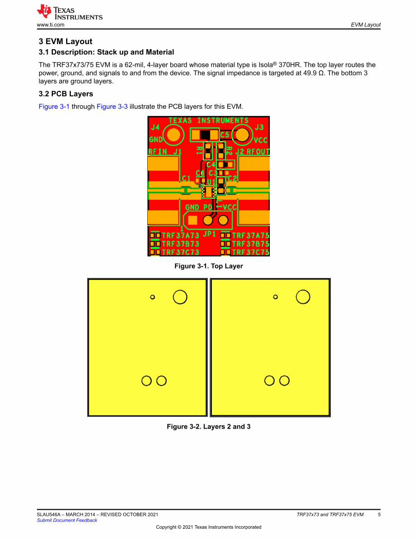
3 EVM Layout3.1 Description: Stack up and MaterialThe TRF37x73/75 EVM is a 62-mil, 4-layer board whose material type is Isola® 370HR. The top layer routes the power, ground, and signals to and from the device. The signal impedance is targeted at 49.9 Ω. The bottom 3 layers are ground layers.
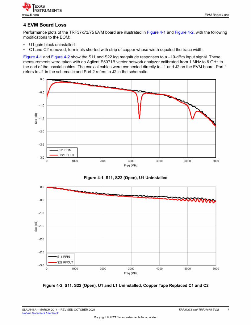
3.2 PCB LayersFigure 3-1 through Figure 3-3 illustrate the PCB layers for this EVM.
Figure 3-1. Top Layer
Figure 3-2. Layers 2 and 3
www.ti.com EVM Layout
SLAU546A – MARCH 2014 – REVISED OCTOBER 2021Submit Document Feedback
TRF37x73 and TRF37x75 EVM 5
Copyright © 2021 Texas Instruments Incorporated

Figure 3-3. Bottom Layer (Through Top Side)
EVM Layout www.ti.com
6 TRF37x73 and TRF37x75 EVM SLAU546A – MARCH 2014 – REVISED OCTOBER 2021Submit Document Feedback
Copyright © 2021 Texas Instruments Incorporated
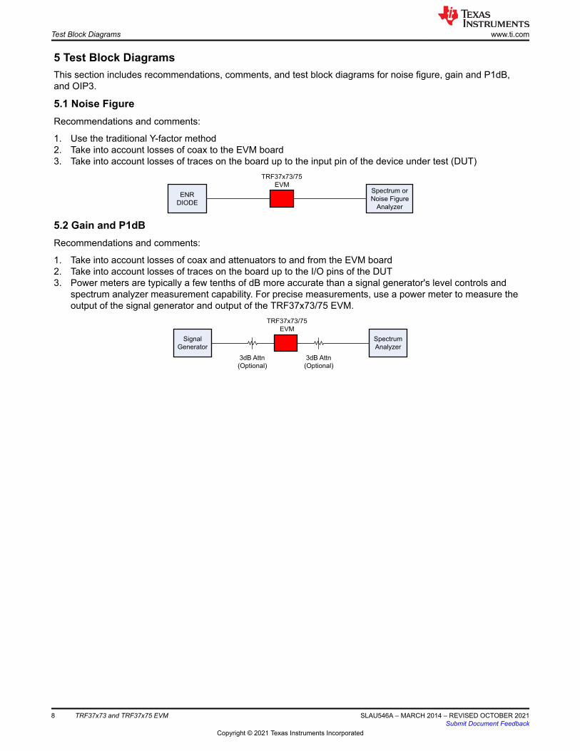
4 EVM Board LossPerformance plots of the TRF37x73/75 EVM board are illustrated in Figure 4-1 and Figure 4-2, with the following modifications to the BOM:
• U1 gain block uninstalled• C1 and C2 removed, terminals shorted with strip of copper whose width equaled the trace width.
Figure 4-1 and Figure 4-2 show the S11 and S22 log magnitude responses to a –10-dBm input signal. These measurements were taken with an Agilent E5071B vector network analyzer calibrated from 1 MHz to 6 GHz to the end of the coaxial cables. The coaxial cables were connected directly to J1 and J2 on the EVM board. Port 1 refers to J1 in the schematic and Port 2 refers to J2 in the schematic.
±3.0
±2.5
±2.0
±1.5
±1.0
±0.5
0.0
0 1000 2000 3000 4000 5000 6000
Sxx (
dB
)
Freq (MHz)
S11 RFIN
S22 RFOUT
C001
Figure 4-1. S11, S22 (Open), U1 Uninstalled
±3.0
±2.5
±2.0
±1.5
±1.0
±0.5
0.0
0 1000 2000 3000 4000 5000 6000
Sxx (
dB
)
Freq (MHz)
S11 RFIN
S22 RFOUT
C002
Figure 4-2. S11, S22 (Open), U1 and L1 Uninstalled, Copper Tape Replaced C1 and C2
www.ti.com EVM Board Loss
SLAU546A – MARCH 2014 – REVISED OCTOBER 2021Submit Document Feedback
TRF37x73 and TRF37x75 EVM 7
Copyright © 2021 Texas Instruments Incorporated
5 Test Block DiagramsThis section includes recommendations, comments, and test block diagrams for noise figure, gain and P1dB, and OIP3.
5.1 Noise FigureRecommendations and comments:
1. Use the traditional Y-factor method2. Take into account losses of coax to the EVM board3. Take into account losses of traces on the board up to the input pin of the device under test (DUT)
TRF37x73/75
EVMSpectrum or
Noise Figure
Analyzer
ENR
DIODE
5.2 Gain and P1dBRecommendations and comments:
1. Take into account losses of coax and attenuators to and from the EVM board2. Take into account losses of traces on the board up to the I/O pins of the DUT3. Power meters are typically a few tenths of dB more accurate than a signal generator's level controls and
spectrum analyzer measurement capability. For precise measurements, use a power meter to measure the output of the signal generator and output of the TRF37x73/75 EVM.
TRF37x73/75
EVM
Spectrum
Analyzer
3dB Attn
(Optional)
Signal
Generator
3dB Attn
(Optional)
Test Block Diagrams www.ti.com
8 TRF37x73 and TRF37x75 EVM SLAU546A – MARCH 2014 – REVISED OCTOBER 2021Submit Document Feedback
Copyright © 2021 Texas Instruments Incorporated

5.3 OIP3Recommendations and comments:
1. This setup can also be used for gain and P1dB, if desired2. For wideband measurements, the 30-dB gain stage and 10-dB attenuators are used to improve the input
IP3 level that is created from the interaction of the 2 signal generators via the isolation of the combiner. For narrow band measurements, it maybe possible to create a setup with enough isolation using an isolator and/or combiner. In this case the 10-dB pads could be reduced or removed.
3. Power meter A is used to ensure the amplitude of the two tones at the input of the TRF37x73/75 EVM are within a certain tolerance. The gain stages will have unique gain characteristics and their gain can drift over time
4. Power meter B can be used for measuring the amplitude of individual tones for more accurate measurements.
5. Keep spectrum analyzer RBW and VBW settings identical for main tone and IM3 products6. Take into account losses of coax and attenuators to and from the EVM board7. Take into account losses of traces on the board up to the I/O pins of the DUT
30dB Gain
30dB Gain
10dB Attn
10dB Attn
Combiner
Power MeterInput A
Coupler
3dB Attn
3dB Attn
Signal
Generator
A
Signal
Generator
B
TRF37x73/75
EVM
SpectrumAnalyzer
3dB AttnSplitter orCoupler
Power MeterInput B
3dB Attn
3dB Attn
6 Revision HistoryNOTE: Page numbers for previous revisions may differ from page numbers in the current version.
Changes from Revision * (March 2014) to Revision A (October 2021) Page• Updated the numbering format for tables, figures, and cross-references throughout the document..................2• Updated the L1 components part number from -6-3HP-F10XJLU to 0603HP-R10XJLW in the TRF37x73/75
EVM BOM table.................................................................................................................................................. 3
www.ti.com Test Block Diagrams
SLAU546A – MARCH 2014 – REVISED OCTOBER 2021Submit Document Feedback
TRF37x73 and TRF37x75 EVM 9
Copyright © 2021 Texas Instruments Incorporated

STANDARD TERMS FOR EVALUATION MODULES1. Delivery: TI delivers TI evaluation boards, kits, or modules, including any accompanying demonstration software, components, and/or
documentation which may be provided together or separately (collectively, an “EVM” or “EVMs”) to the User (“User”) in accordancewith the terms set forth herein. User's acceptance of the EVM is expressly subject to the following terms.1.1 EVMs are intended solely for product or software developers for use in a research and development setting to facilitate feasibility
evaluation, experimentation, or scientific analysis of TI semiconductors products. EVMs have no direct function and are notfinished products. EVMs shall not be directly or indirectly assembled as a part or subassembly in any finished product. Forclarification, any software or software tools provided with the EVM (“Software”) shall not be subject to the terms and conditionsset forth herein but rather shall be subject to the applicable terms that accompany such Software
1.2 EVMs are not intended for consumer or household use. EVMs may not be sold, sublicensed, leased, rented, loaned, assigned,or otherwise distributed for commercial purposes by Users, in whole or in part, or used in any finished product or productionsystem.
2 Limited Warranty and Related Remedies/Disclaimers:2.1 These terms do not apply to Software. The warranty, if any, for Software is covered in the applicable Software License
Agreement.2.2 TI warrants that the TI EVM will conform to TI's published specifications for ninety (90) days after the date TI delivers such EVM
to User. Notwithstanding the foregoing, TI shall not be liable for a nonconforming EVM if (a) the nonconformity was caused byneglect, misuse or mistreatment by an entity other than TI, including improper installation or testing, or for any EVMs that havebeen altered or modified in any way by an entity other than TI, (b) the nonconformity resulted from User's design, specificationsor instructions for such EVMs or improper system design, or (c) User has not paid on time. Testing and other quality controltechniques are used to the extent TI deems necessary. TI does not test all parameters of each EVM.User's claims against TI under this Section 2 are void if User fails to notify TI of any apparent defects in the EVMs within ten (10)business days after delivery, or of any hidden defects with ten (10) business days after the defect has been detected.
2.3 TI's sole liability shall be at its option to repair or replace EVMs that fail to conform to the warranty set forth above, or creditUser's account for such EVM. TI's liability under this warranty shall be limited to EVMs that are returned during the warrantyperiod to the address designated by TI and that are determined by TI not to conform to such warranty. If TI elects to repair orreplace such EVM, TI shall have a reasonable time to repair such EVM or provide replacements. Repaired EVMs shall bewarranted for the remainder of the original warranty period. Replaced EVMs shall be warranted for a new full ninety (90) daywarranty period.
WARNINGEvaluation Kits are intended solely for use by technically qualified,professional electronics experts who are familiar with the dangers
and application risks associated with handling electrical mechanicalcomponents, systems, and subsystems.
User shall operate the Evaluation Kit within TI’s recommendedguidelines and any applicable legal or environmental requirementsas well as reasonable and customary safeguards. Failure to set up
and/or operate the Evaluation Kit within TI’s recommendedguidelines may result in personal injury or death or propertydamage. Proper set up entails following TI’s instructions for
electrical ratings of interface circuits such as input, output andelectrical loads.
NOTE:EXPOSURE TO ELECTROSTATIC DISCHARGE (ESD) MAY CAUSE DEGREDATION OR FAILURE OF THE EVALUATIONKIT; TI RECOMMENDS STORAGE OF THE EVALUATION KIT IN A PROTECTIVE ESD BAG.
www.ti.com
2
3 Regulatory Notices:3.1 United States
3.1.1 Notice applicable to EVMs not FCC-Approved:FCC NOTICE: This kit is designed to allow product developers to evaluate electronic components, circuitry, or softwareassociated with the kit to determine whether to incorporate such items in a finished product and software developers to writesoftware applications for use with the end product. This kit is not a finished product and when assembled may not be resold orotherwise marketed unless all required FCC equipment authorizations are first obtained. Operation is subject to the conditionthat this product not cause harmful interference to licensed radio stations and that this product accept harmful interference.Unless the assembled kit is designed to operate under part 15, part 18 or part 95 of this chapter, the operator of the kit mustoperate under the authority of an FCC license holder or must secure an experimental authorization under part 5 of this chapter.3.1.2 For EVMs annotated as FCC – FEDERAL COMMUNICATIONS COMMISSION Part 15 Compliant:
CAUTIONThis device complies with part 15 of the FCC Rules. Operation is subject to the following two conditions: (1) This device may notcause harmful interference, and (2) this device must accept any interference received, including interference that may causeundesired operation.Changes or modifications not expressly approved by the party responsible for compliance could void the user's authority tooperate the equipment.
FCC Interference Statement for Class A EVM devicesNOTE: This equipment has been tested and found to comply with the limits for a Class A digital device, pursuant to part 15 ofthe FCC Rules. These limits are designed to provide reasonable protection against harmful interference when the equipment isoperated in a commercial environment. This equipment generates, uses, and can radiate radio frequency energy and, if notinstalled and used in accordance with the instruction manual, may cause harmful interference to radio communications.Operation of this equipment in a residential area is likely to cause harmful interference in which case the user will be required tocorrect the interference at his own expense.
FCC Interference Statement for Class B EVM devicesNOTE: This equipment has been tested and found to comply with the limits for a Class B digital device, pursuant to part 15 ofthe FCC Rules. These limits are designed to provide reasonable protection against harmful interference in a residentialinstallation. This equipment generates, uses and can radiate radio frequency energy and, if not installed and used in accordancewith the instructions, may cause harmful interference to radio communications. However, there is no guarantee that interferencewill not occur in a particular installation. If this equipment does cause harmful interference to radio or television reception, whichcan be determined by turning the equipment off and on, the user is encouraged to try to correct the interference by one or moreof the following measures:
• Reorient or relocate the receiving antenna.• Increase the separation between the equipment and receiver.• Connect the equipment into an outlet on a circuit different from that to which the receiver is connected.• Consult the dealer or an experienced radio/TV technician for help.
3.2 Canada3.2.1 For EVMs issued with an Industry Canada Certificate of Conformance to RSS-210 or RSS-247
Concerning EVMs Including Radio Transmitters:This device complies with Industry Canada license-exempt RSSs. Operation is subject to the following two conditions:(1) this device may not cause interference, and (2) this device must accept any interference, including interference that maycause undesired operation of the device.
Concernant les EVMs avec appareils radio:Le présent appareil est conforme aux CNR d'Industrie Canada applicables aux appareils radio exempts de licence. L'exploitationest autorisée aux deux conditions suivantes: (1) l'appareil ne doit pas produire de brouillage, et (2) l'utilisateur de l'appareil doitaccepter tout brouillage radioélectrique subi, même si le brouillage est susceptible d'en compromettre le fonctionnement.
Concerning EVMs Including Detachable Antennas:Under Industry Canada regulations, this radio transmitter may only operate using an antenna of a type and maximum (or lesser)gain approved for the transmitter by Industry Canada. To reduce potential radio interference to other users, the antenna typeand its gain should be so chosen that the equivalent isotropically radiated power (e.i.r.p.) is not more than that necessary forsuccessful communication. This radio transmitter has been approved by Industry Canada to operate with the antenna typeslisted in the user guide with the maximum permissible gain and required antenna impedance for each antenna type indicated.Antenna types not included in this list, having a gain greater than the maximum gain indicated for that type, are strictly prohibitedfor use with this device.
www.ti.com
3
Concernant les EVMs avec antennes détachablesConformément à la réglementation d'Industrie Canada, le présent émetteur radio peut fonctionner avec une antenne d'un type etd'un gain maximal (ou inférieur) approuvé pour l'émetteur par Industrie Canada. Dans le but de réduire les risques de brouillageradioélectrique à l'intention des autres utilisateurs, il faut choisir le type d'antenne et son gain de sorte que la puissance isotroperayonnée équivalente (p.i.r.e.) ne dépasse pas l'intensité nécessaire à l'établissement d'une communication satisfaisante. Leprésent émetteur radio a été approuvé par Industrie Canada pour fonctionner avec les types d'antenne énumérés dans lemanuel d’usage et ayant un gain admissible maximal et l'impédance requise pour chaque type d'antenne. Les types d'antennenon inclus dans cette liste, ou dont le gain est supérieur au gain maximal indiqué, sont strictement interdits pour l'exploitation del'émetteur
3.3 Japan3.3.1 Notice for EVMs delivered in Japan: Please see http://www.tij.co.jp/lsds/ti_ja/general/eStore/notice_01.page 日本国内に
輸入される評価用キット、ボードについては、次のところをご覧ください。http://www.tij.co.jp/lsds/ti_ja/general/eStore/notice_01.page
3.3.2 Notice for Users of EVMs Considered “Radio Frequency Products” in Japan: EVMs entering Japan may not be certifiedby TI as conforming to Technical Regulations of Radio Law of Japan.
If User uses EVMs in Japan, not certified to Technical Regulations of Radio Law of Japan, User is required to follow theinstructions set forth by Radio Law of Japan, which includes, but is not limited to, the instructions below with respect to EVMs(which for the avoidance of doubt are stated strictly for convenience and should be verified by User):1. Use EVMs in a shielded room or any other test facility as defined in the notification #173 issued by Ministry of Internal
Affairs and Communications on March 28, 2006, based on Sub-section 1.1 of Article 6 of the Ministry’s Rule forEnforcement of Radio Law of Japan,
2. Use EVMs only after User obtains the license of Test Radio Station as provided in Radio Law of Japan with respect toEVMs, or
3. Use of EVMs only after User obtains the Technical Regulations Conformity Certification as provided in Radio Law of Japanwith respect to EVMs. Also, do not transfer EVMs, unless User gives the same notice above to the transferee. Please notethat if User does not follow the instructions above, User will be subject to penalties of Radio Law of Japan.
【無線電波を送信する製品の開発キットをお使いになる際の注意事項】 開発キットの中には技術基準適合証明を受けていないものがあります。 技術適合証明を受けていないもののご使用に際しては、電波法遵守のため、以下のいずれかの措置を取っていただく必要がありますのでご注意ください。1. 電波法施行規則第6条第1項第1号に基づく平成18年3月28日総務省告示第173号で定められた電波暗室等の試験設備でご使用
いただく。2. 実験局の免許を取得後ご使用いただく。3. 技術基準適合証明を取得後ご使用いただく。
なお、本製品は、上記の「ご使用にあたっての注意」を譲渡先、移転先に通知しない限り、譲渡、移転できないものとします。上記を遵守頂けない場合は、電波法の罰則が適用される可能性があることをご留意ください。 日本テキサス・イ
ンスツルメンツ株式会社東京都新宿区西新宿6丁目24番1号西新宿三井ビル
3.3.3 Notice for EVMs for Power Line Communication: Please see http://www.tij.co.jp/lsds/ti_ja/general/eStore/notice_02.page電力線搬送波通信についての開発キットをお使いになる際の注意事項については、次のところをご覧ください。http://www.tij.co.jp/lsds/ti_ja/general/eStore/notice_02.page
3.4 European Union3.4.1 For EVMs subject to EU Directive 2014/30/EU (Electromagnetic Compatibility Directive):
This is a class A product intended for use in environments other than domestic environments that are connected to alow-voltage power-supply network that supplies buildings used for domestic purposes. In a domestic environment thisproduct may cause radio interference in which case the user may be required to take adequate measures.
www.ti.com
4
4 EVM Use Restrictions and Warnings:4.1 EVMS ARE NOT FOR USE IN FUNCTIONAL SAFETY AND/OR SAFETY CRITICAL EVALUATIONS, INCLUDING BUT NOT
LIMITED TO EVALUATIONS OF LIFE SUPPORT APPLICATIONS.4.2 User must read and apply the user guide and other available documentation provided by TI regarding the EVM prior to handling
or using the EVM, including without limitation any warning or restriction notices. The notices contain important safety informationrelated to, for example, temperatures and voltages.
4.3 Safety-Related Warnings and Restrictions:4.3.1 User shall operate the EVM within TI’s recommended specifications and environmental considerations stated in the user
guide, other available documentation provided by TI, and any other applicable requirements and employ reasonable andcustomary safeguards. Exceeding the specified performance ratings and specifications (including but not limited to inputand output voltage, current, power, and environmental ranges) for the EVM may cause personal injury or death, orproperty damage. If there are questions concerning performance ratings and specifications, User should contact a TIfield representative prior to connecting interface electronics including input power and intended loads. Any loads appliedoutside of the specified output range may also result in unintended and/or inaccurate operation and/or possiblepermanent damage to the EVM and/or interface electronics. Please consult the EVM user guide prior to connecting anyload to the EVM output. If there is uncertainty as to the load specification, please contact a TI field representative.During normal operation, even with the inputs and outputs kept within the specified allowable ranges, some circuitcomponents may have elevated case temperatures. These components include but are not limited to linear regulators,switching transistors, pass transistors, current sense resistors, and heat sinks, which can be identified using theinformation in the associated documentation. When working with the EVM, please be aware that the EVM may becomevery warm.
4.3.2 EVMs are intended solely for use by technically qualified, professional electronics experts who are familiar with thedangers and application risks associated with handling electrical mechanical components, systems, and subsystems.User assumes all responsibility and liability for proper and safe handling and use of the EVM by User or its employees,affiliates, contractors or designees. User assumes all responsibility and liability to ensure that any interfaces (electronicand/or mechanical) between the EVM and any human body are designed with suitable isolation and means to safelylimit accessible leakage currents to minimize the risk of electrical shock hazard. User assumes all responsibility andliability for any improper or unsafe handling or use of the EVM by User or its employees, affiliates, contractors ordesignees.
4.4 User assumes all responsibility and liability to determine whether the EVM is subject to any applicable international, federal,state, or local laws and regulations related to User’s handling and use of the EVM and, if applicable, User assumes allresponsibility and liability for compliance in all respects with such laws and regulations. User assumes all responsibility andliability for proper disposal and recycling of the EVM consistent with all applicable international, federal, state, and localrequirements.
5. Accuracy of Information: To the extent TI provides information on the availability and function of EVMs, TI attempts to be as accurateas possible. However, TI does not warrant the accuracy of EVM descriptions, EVM availability or other information on its websites asaccurate, complete, reliable, current, or error-free.
6. Disclaimers:6.1 EXCEPT AS SET FORTH ABOVE, EVMS AND ANY MATERIALS PROVIDED WITH THE EVM (INCLUDING, BUT NOT
LIMITED TO, REFERENCE DESIGNS AND THE DESIGN OF THE EVM ITSELF) ARE PROVIDED "AS IS" AND "WITH ALLFAULTS." TI DISCLAIMS ALL OTHER WARRANTIES, EXPRESS OR IMPLIED, REGARDING SUCH ITEMS, INCLUDING BUTNOT LIMITED TO ANY EPIDEMIC FAILURE WARRANTY OR IMPLIED WARRANTIES OF MERCHANTABILITY OR FITNESSFOR A PARTICULAR PURPOSE OR NON-INFRINGEMENT OF ANY THIRD PARTY PATENTS, COPYRIGHTS, TRADESECRETS OR OTHER INTELLECTUAL PROPERTY RIGHTS.
6.2 EXCEPT FOR THE LIMITED RIGHT TO USE THE EVM SET FORTH HEREIN, NOTHING IN THESE TERMS SHALL BECONSTRUED AS GRANTING OR CONFERRING ANY RIGHTS BY LICENSE, PATENT, OR ANY OTHER INDUSTRIAL ORINTELLECTUAL PROPERTY RIGHT OF TI, ITS SUPPLIERS/LICENSORS OR ANY OTHER THIRD PARTY, TO USE THEEVM IN ANY FINISHED END-USER OR READY-TO-USE FINAL PRODUCT, OR FOR ANY INVENTION, DISCOVERY ORIMPROVEMENT, REGARDLESS OF WHEN MADE, CONCEIVED OR ACQUIRED.
7. USER'S INDEMNITY OBLIGATIONS AND REPRESENTATIONS. USER WILL DEFEND, INDEMNIFY AND HOLD TI, ITSLICENSORS AND THEIR REPRESENTATIVES HARMLESS FROM AND AGAINST ANY AND ALL CLAIMS, DAMAGES, LOSSES,EXPENSES, COSTS AND LIABILITIES (COLLECTIVELY, "CLAIMS") ARISING OUT OF OR IN CONNECTION WITH ANYHANDLING OR USE OF THE EVM THAT IS NOT IN ACCORDANCE WITH THESE TERMS. THIS OBLIGATION SHALL APPLYWHETHER CLAIMS ARISE UNDER STATUTE, REGULATION, OR THE LAW OF TORT, CONTRACT OR ANY OTHER LEGALTHEORY, AND EVEN IF THE EVM FAILS TO PERFORM AS DESCRIBED OR EXPECTED.

www.ti.com
5
8. Limitations on Damages and Liability:8.1 General Limitations. IN NO EVENT SHALL TI BE LIABLE FOR ANY SPECIAL, COLLATERAL, INDIRECT, PUNITIVE,
INCIDENTAL, CONSEQUENTIAL, OR EXEMPLARY DAMAGES IN CONNECTION WITH OR ARISING OUT OF THESETERMS OR THE USE OF THE EVMS , REGARDLESS OF WHETHER TI HAS BEEN ADVISED OF THE POSSIBILITY OFSUCH DAMAGES. EXCLUDED DAMAGES INCLUDE, BUT ARE NOT LIMITED TO, COST OF REMOVAL ORREINSTALLATION, ANCILLARY COSTS TO THE PROCUREMENT OF SUBSTITUTE GOODS OR SERVICES, RETESTING,OUTSIDE COMPUTER TIME, LABOR COSTS, LOSS OF GOODWILL, LOSS OF PROFITS, LOSS OF SAVINGS, LOSS OFUSE, LOSS OF DATA, OR BUSINESS INTERRUPTION. NO CLAIM, SUIT OR ACTION SHALL BE BROUGHT AGAINST TIMORE THAN TWELVE (12) MONTHS AFTER THE EVENT THAT GAVE RISE TO THE CAUSE OF ACTION HASOCCURRED.
8.2 Specific Limitations. IN NO EVENT SHALL TI'S AGGREGATE LIABILITY FROM ANY USE OF AN EVM PROVIDEDHEREUNDER, INCLUDING FROM ANY WARRANTY, INDEMITY OR OTHER OBLIGATION ARISING OUT OF OR INCONNECTION WITH THESE TERMS, , EXCEED THE TOTAL AMOUNT PAID TO TI BY USER FOR THE PARTICULAREVM(S) AT ISSUE DURING THE PRIOR TWELVE (12) MONTHS WITH RESPECT TO WHICH LOSSES OR DAMAGES ARECLAIMED. THE EXISTENCE OF MORE THAN ONE CLAIM SHALL NOT ENLARGE OR EXTEND THIS LIMIT.
9. Return Policy. Except as otherwise provided, TI does not offer any refunds, returns, or exchanges. Furthermore, no return of EVM(s)will be accepted if the package has been opened and no return of the EVM(s) will be accepted if they are damaged or otherwise not ina resalable condition. If User feels it has been incorrectly charged for the EVM(s) it ordered or that delivery violates the applicableorder, User should contact TI. All refunds will be made in full within thirty (30) working days from the return of the components(s),excluding any postage or packaging costs.
10. Governing Law: These terms and conditions shall be governed by and interpreted in accordance with the laws of the State of Texas,without reference to conflict-of-laws principles. User agrees that non-exclusive jurisdiction for any dispute arising out of or relating tothese terms and conditions lies within courts located in the State of Texas and consents to venue in Dallas County, Texas.Notwithstanding the foregoing, any judgment may be enforced in any United States or foreign court, and TI may seek injunctive reliefin any United States or foreign court.
Mailing Address: Texas Instruments, Post Office Box 655303, Dallas, Texas 75265Copyright © 2019, Texas Instruments Incorporated
IMPORTANT NOTICE AND DISCLAIMERTI PROVIDES TECHNICAL AND RELIABILITY DATA (INCLUDING DATA SHEETS), DESIGN RESOURCES (INCLUDING REFERENCE DESIGNS), APPLICATION OR OTHER DESIGN ADVICE, WEB TOOLS, SAFETY INFORMATION, AND OTHER RESOURCES “AS IS” AND WITH ALL FAULTS, AND DISCLAIMS ALL WARRANTIES, EXPRESS AND IMPLIED, INCLUDING WITHOUT LIMITATION ANY IMPLIED WARRANTIES OF MERCHANTABILITY, FITNESS FOR A PARTICULAR PURPOSE OR NON-INFRINGEMENT OF THIRD PARTY INTELLECTUAL PROPERTY RIGHTS.These resources are intended for skilled developers designing with TI products. You are solely responsible for (1) selecting the appropriate TI products for your application, (2) designing, validating and testing your application, and (3) ensuring your application meets applicable standards, and any other safety, security, regulatory or other requirements.These resources are subject to change without notice. TI grants you permission to use these resources only for development of an application that uses the TI products described in the resource. Other reproduction and display of these resources is prohibited. No license is granted to any other TI intellectual property right or to any third party intellectual property right. TI disclaims responsibility for, and you will fully indemnify TI and its representatives against, any claims, damages, costs, losses, and liabilities arising out of your use of these resources.TI’s products are provided subject to TI’s Terms of Sale or other applicable terms available either on ti.com or provided in conjunction with such TI products. TI’s provision of these resources does not expand or otherwise alter TI’s applicable warranties or warranty disclaimers for TI products.TI objects to and rejects any additional or different terms you may have proposed. IMPORTANT NOTICE
Mailing Address: Texas Instruments, Post Office Box 655303, Dallas, Texas 75265Copyright © 2021, Texas Instruments Incorporated