Embed Size (px)
Citation preview
1
Mechanics of Contact and Lubrication – ME5656 Department of Mechanical & Industrial Engineering
Northeastern University Fall 2011
Tribology of Electrical Contacts
Richard Gilley
Northeastern University 360 Huntington Ave. Boston, MA 02115
ABSTRACT The electrical contact resistance of a contact pair is a characteristic that strongly influences
contact life. Scientists and Engineers have rigorously studied the mechanics behind conductive contacts
in order to understand and model their behavior. Of critical importance is accurately modeling electrical
contact resistance of rough contact members. An accurate model will lead to robust electrical contact
designs and increased life for the given application and scale. Statistical, multi‐scale roughness and
fractal geometry are a few examples of models that have been created to model electrical contact
resistance. These models have been successful in eliminating flaws and building on previous models.
As electronic devices become increasingly smaller, there is a need to apply these models to micro and
nano‐scale contacts. Scientists and engineers will continue to work diligently in modeling electrical
contact resistance so that micro and nano‐scale devices are as robust as macro scale devices.
2
1.0 INTRODUCTIONElectronic devices are becoming increasingly important in this technological age. Of particular
importance are tribological studies of stationary and sliding electrical contacts. There is an increasing
demand for contacts that can withstand higher currents and have a longer service life in the macro and
micro scales. As with most electronics, electrical contacts are following the trend of reduced size while
requiring equal or better performance. Analyzing electrical contacts on a tribological level has provided
insight about the mechanics responsible for friction, wear and lubrication. Tribological characteristics
such as these play a role in the electrical contact resistance and contact life. Of equal importance are
surface roughness characteristics and how these characteristics contribute to electrical contact
resistance. This necessitates the need for accurate models to determine the electrical contact
resistance, or ECR, based on a surface profile. Accurate knowledge of ECR can lead to the development
of robust designs for the given application and scale. This paper will provide an overview of electrical
contacts and review the key contact resistance principles presented by Holm and Greenwood. This will
be followed by a review of statistical, multi‐scale roughness and fractal geometry models used to predict
ECR. This paper will close with a review of open problems in the field and the future state of tribological
issues of electrical contacts. It should be noted that this review touches the surface of ECR and is only a
brief review of a select group of modeling techniques. There are numerous other modeling techniques
to determine ECR and many other factors such as friction, lubrication and wear that contribute to ECR.
2.0 OVERVIEWSurfaces, when viewed under a microscope, have many defining characteristics that the human
eye is unable to see. Surfaces are generally defined by their roughness, which consists of peaks and
valleys of varying heights and depths. The peaks and valleys of man‐made surfaces are generated by
different manufacturing and finishing processes. When two bodies are in contact, the true contact area
is significantly less than the nominal contact area [8]. Actual contact takes places at the peaks of the
surfaces that are coincident. Two surfaces in intermittent contact that carry electrical current are
known as electrical contacts. The two electrical conductors are simply know as contacts; one being the
anode and the other the cathode. Contacts that are electrically connected are referred to as closed
contacts. Contacts that are separated so that there is no current flow are referred to as open contacts
[5]. The constriction that impedes current flow between electrical contacts is referred to as contact
resistance. Two basic theories that laid the foundation to contact resistance will be discussed.
3
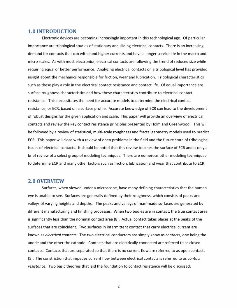
2.1Holm’sTheory Holm’s theory laid a foundation from which many other theories have been created. The actual
current flow between two contacting surfaces takes places through small circular spots. These surface
irregularities that conduct electricity are known as circular a‐spots. The current flow lines bend as they
pass through a‐spots as seen in Figure 1. The restriction of current flow through the small conducting
spots leads to constriction resistance which adds to the overall contact resistance [5].
Figure 1 ‐ Current flow through a‐spots [8]
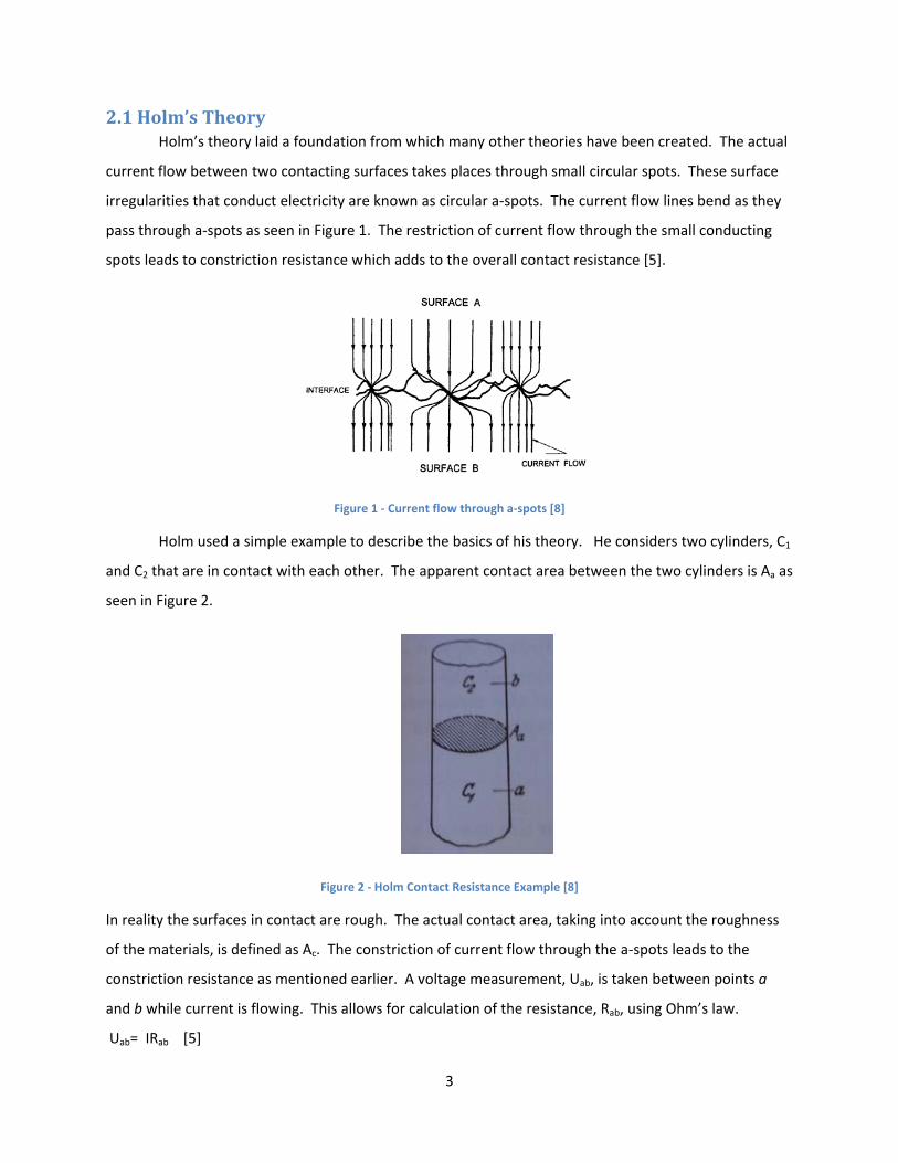
Holm used a simple example to describe the basics of his theory. He considers two cylinders, C1
and C2 that are in contact with each other. The apparent contact area between the two cylinders is Aa as
seen in Figure 2.
Figure 2 ‐ Holm Contact Resistance Example [8]
In reality the surfaces in contact are rough. The actual contact area, taking into account the roughness
of the materials, is defined as Ac. The constriction of current flow through the a‐spots leads to the
constriction resistance as mentioned earlier. A voltage measurement, Uab, is taken between points a
and b while current is flowing. This allows for calculation of the resistance, Rab, using Ohm’s law.
Uab= IRab [5]
4
Holm then assumes that the current flows through area Aa. This area is perfectly smooth and does not
contain a‐spots. A measurement is then taken across points a and b with current flowing to obtain the
resistance R0ab. The constriction resistance, Rc, equals
Rc= R0ab ‐ Rab [5]
If there is absence of a film resistance on the contact surfaces, then the contact resistance is equal to
the constriction resistance. If there are film resistances, then the contact resistance is the sum of the
constriction resistance and the film resistance. The contact resistance, R, for contacts of different
materials and a film resistance is
R=Rc1+Rc2+Rfilm [5]
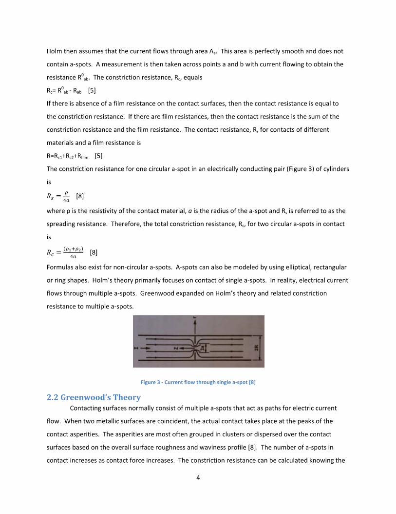
The constriction resistance for one circular a‐spot in an electrically conducting pair (Figure 3) of cylinders
is
[8]
where ρ is the resistivity of the contact material, a is the radius of the a‐spot and Rs is referred to as the
spreading resistance. Therefore, the total constriction resistance, Rc, for two circular a‐spots in contact
is
[8]
Formulas also exist for non‐circular a‐spots. A‐spots can also be modeled by using elliptical, rectangular
or ring shapes. Holm’s theory primarily focuses on contact of single a‐spots. In reality, electrical current
flows through multiple a‐spots. Greenwood expanded on Holm’s theory and related constriction
resistance to multiple a‐spots.
Figure 3 ‐ Current flow through single a‐spot [8]
2.2Greenwood’sTheory Contacting surfaces normally consist of multiple a‐spots that act as paths for electric current
flow. When two metallic surfaces are coincident, the actual contact takes place at the peaks of the
contact asperities. The asperities are most often grouped in clusters or dispersed over the contact
surfaces based on the overall surface roughness and waviness profile [8]. The number of a‐spots in
contact increases as contact force increases. The constriction resistance can be calculated knowing the

5
size and location of the a‐spots. Film resistance can reduce the number of a‐spots that actually conduct
electricity. This makes is difficult to quantify the number of a‐spots in contact. Greenwood’s basic
equation for contact resistance of a large quantity of a‐spots within a single cluster is
[8]
where ρ is the resistivity of the contact material, n is the number of circular a‐spots, a is the mean a‐spot
radius and α is the radius of the cluster. The cluster radius is also referred to as the Holm radius [8]. The
1/2na term is the a‐spot resistance and the 1/2α term is the cluster resistance.
An array of 76 identical a‐spots can be seen in Figure 4. The shaded portion of the figure is a
single continuous contact that has an equivalent resistance to the array of 76 a‐spots. The outer circle is
the Holm Radius, α.
Figure 4 ‐ Array of 76 identical a‐spots with Holm Radius (outer circle) and a single continuous contact of same resistance (shaded circle) [8]
Greenwood calculated the effect of the a‐spot radius on the a‐spot and cluster resistance. The results
can be seen in Table 1 along with the Holm radius, α, and the radius of a single spot of comparable
resistance. It can be seen that as the a‐spot radius increases, the a‐spot and cluster resistance decrease.
It can also be seen that for an a‐spot radius of approximately .05, the cluster resistance is more than the
a‐spot resistance. The results told Greenwood that the number and distribution of the a‐spots does not
have a significant effect on the contact resistance [8]. This assumption assumes that the a‐spots are
evenly distributed and there is no film resistance.
a‐Spot Radiusa‐Spot Resistance,
1/2na
Holm Radius,
α
Cluster Resistance,
1/2α
Radius of Single Spot of
Same Resistance
0.02 0.3289 5.34 0.0937 1.18
0.04 0.1645 5.36 0.0932 1.94
0.10 0.0658 5.42 0.0923 3.16
0.20 0.0329 5.50 0.0909 4.04
0.50 0.0132 5.68 0.0880 4.94
Table 1 ‐ Effect of a‐Spot radius on resistance [8]
6
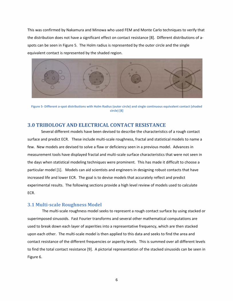
This was confirmed by Nakamura and Minowa who used FEM and Monte Carlo techniques to verify that
the distribution does not have a significant effect on contact resistance [8]. Different distributions of a‐
spots can be seen in Figure 5. The Holm radius is represented by the outer circle and the single
equivalent contact is represented by the shaded region.
Figure 5‐ Different a‐spot distributions with Holm Radius (outer circle) and single continuous equivalent contact (shaded circle) [8]
3.0 TRIBOLOGYANDELECTRICALCONTACTRESISTANCE Several different models have been devised to describe the characteristics of a rough contact
surface and predict ECR. These include multi‐scale roughness, fractal and statistical models to name a
few. New models are devised to solve a flaw or deficiency seen in a previous model. Advances in
measurement tools have displayed fractal and multi‐scale surface characteristics that were not seen in
the days when statistical modeling techniques were prominent. This has made it difficult to choose a
particular model [1]. Models can aid scientists and engineers in designing robust contacts that have
increased life and lower ECR. The goal is to devise models that accurately reflect and predict
experimental results. The following sections provide a high level review of models used to calculate
ECR.
3.1Multi‐scaleRoughnessModel The multi‐scale roughness model seeks to represent a rough contact surface by using stacked or
superimposed sinusoids. Fast Fourier transforms and several other mathematical computations are
used to break down each layer of asperities into a representative frequency, which are then stacked
upon each other. The multi‐scale model is then applied to this data and seeks to find the area and
contact resistance of the different frequencies or asperity levels. This is summed over all different levels
to find the total contact resistance [9]. A pictorial representation of the stacked sinusoids can be seen in
Figure 6.
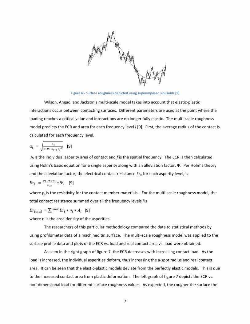
7
Figure 6 ‐ Surface roughness depicted using superimposed sinusoids [9]
Wilson, Angadi and Jackson’s multi‐scale model takes into account that elastic‐plastic
interactions occur between contacting surfaces. Different parameters are used at the point where the
loading reaches a critical value and interactions are no longer fully elastic. The multi‐scale roughness
model predicts the ECR and area for each frequency level i [9]. First, the average radius of the contact is
calculated for each frequency level.
∗ ∗ ∗ [9]
Ai is the individual asperity area of contact and f is the spatial frequency. The ECR is then calculated
using Holm’s basic equation for a single asperity along with an alleviation factor, Ψ. Per Holm’s theory
and the alleviation factor, the electrical contact resistance Eri, for each asperity level, is
∗ [9]
where ρL is the resistivity for the contact member materials. For the multi‐scale roughness model, the
total contact resistance summed over all the frequency levels i is
∑ ∗ ∗ [9]
where η is the area density of the asperities.
The researchers of this particular methodology compared the data to statistical methods by
using profilometer data of a machined tin surface. The multi‐scale roughness model was applied to the
surface profile data and plots of the ECR vs. load and real contact area vs. load were obtained.
As seen in the right graph of figure 7, the ECR decreases with increasing contact load. As the
load is increased, the individual asperities deform, thus increasing the a‐spot radius and real contact
area. It can be seen that the elastic‐plastic models deviate from the perfectly elastic models. This is due
to the increased contact area from plastic deformation. The left graph of figure 7 depicts the ECR vs.
non‐dimensional load for different surface roughness values. As expected, the rougher the surface the
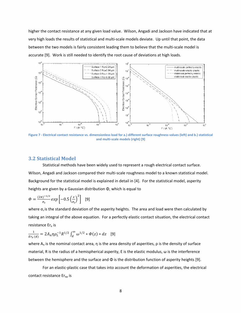
8
higher the contact resistance at any given load value. Wilson, Angadi and Jackson have indicated that at
very high loads the results of statistical and multi‐scale models deviate. Up until that point, the data
between the two models is fairly consistent leading them to believe that the multi‐scale model is
accurate [9]. Work is still needed to identify the root cause of deviations at high loads.
Figure 7 ‐ Electrical contact resistance vs. dimensionless load for a.) different surface roughness values (left) and b.) statistical and multi‐scale models (right) [9]
3.2StatisticalModel Statistical methods have been widely used to represent a rough electrical contact surface.
Wilson, Angadi and Jackson compared their multi‐scale roughness model to a known statistical model.
Background for the statistical model is explained in detail in [4]. For the statistical model, asperity
heights are given by a Gaussian distribution Φ, which is equal to
/0.5 [9]
where σs is the standard deviation of the asperity heights. The area and load were then calculated by
taking an integral of the above equation. For a perfectly elastic contact situation, the electrical contact
resistance Ere is
2 / / ∗ ∗ [9]
where An is the nominal contact area, η is the area density of asperities, ρ is the density of surface
material, R is the radius of a hemispherical asperity, E is the elastic modulus, ω is the interference
between the hemisphere and the surface and Φ is the distribution function of asperity heights [9].
For an elastic‐plastic case that takes into account the deformation of asperities, the electrical
contact resistance Erep is
9
∗ [9]
where aep is the radius of the area of the elastic‐plastic contact. Wilson, Angadi and Jackson use an
alleviation factor, bringing the final elastic‐plastic ECR to
∗ [9]
The results of the comparison of the multi‐scale roughness model to the pre‐existing statistical
model can be seen in the right graph of figure 7. The multi‐scale and statistical models have comparable
data up until high loads are reached as mentioned in the previous section.
3.3FractalGeometryModel A third model presented by Kogut and Komvopoulos uses fractal geometry to characterize a
rough surface. Fractal geometry has the advantage of scale invariance. Scale invariance means that the
measurements are independent of sample length and instrument resolution. With this model, a 3D
surface geometry is created using a modified two‐variable Weierstrass‐Mandelbrot function [6]. This
surface geometry is then used in conjunction with elastic‐plastic surface deformation principles and
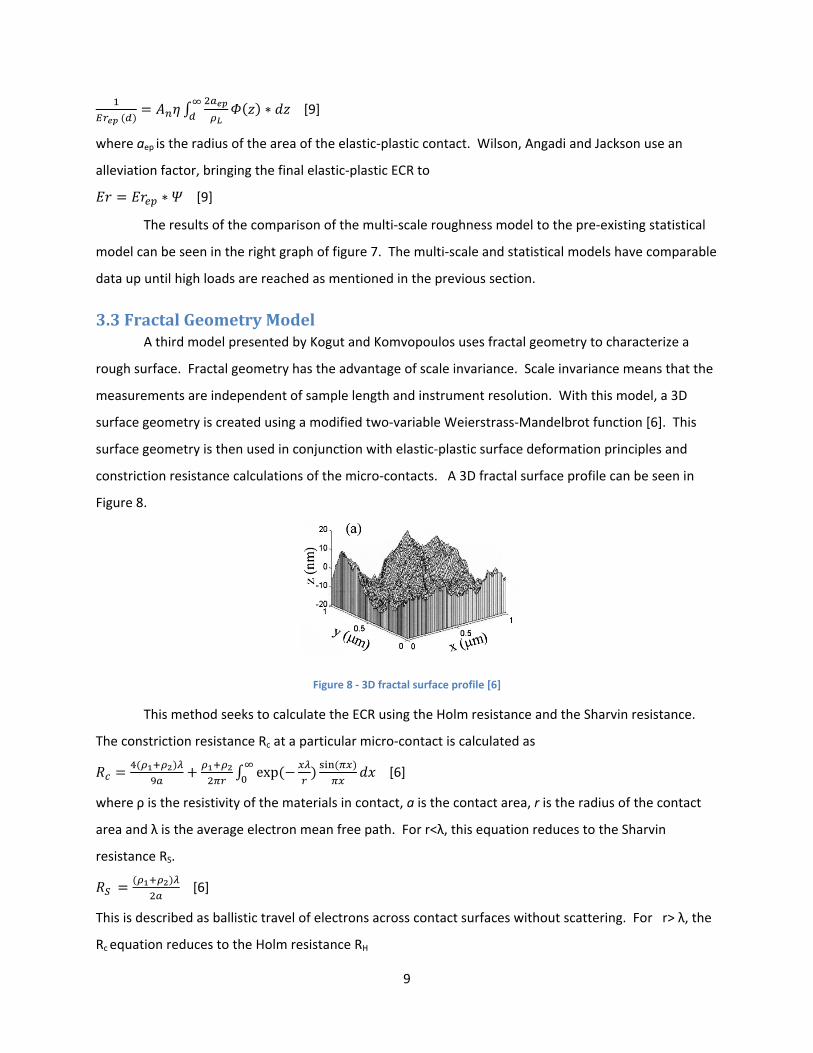
constriction resistance calculations of the micro‐contacts. A 3D fractal surface profile can be seen in
Figure 8.
Figure 8 ‐ 3D fractal surface profile [6]
This method seeks to calculate the ECR using the Holm resistance and the Sharvin resistance.
The constriction resistance Rc at a particular micro‐contact is calculated as
exp
[6]
where ρ is the resistivity of the materials in contact, a is the contact area, r is the radius of the contact
area and λ is the average electron mean free path. For r<λ, this equation reduces to the Sharvin
resistance RS.
[6]
This is described as ballistic travel of electrons across contact surfaces without scattering. For r> λ, the
Rc equation reduces to the Holm resistance RH
10
[6]
where scattering is present. The total electrical contact resistance R taking into account all micro‐
contacts is
∑ [6]
where Rci is the constriction resistance for the ith asperity, and N(a’s) is the number of asperities. R is
then converted into a dimensionless value R*.
The results of this study are based on fractal dimension D and fractal roughness G. Fractal
roughness G is a height scaling parameter. The surface becomes smoother with a decreasing value of G.
The fractal dimension D has to do with high and low frequency components of the Weierstrass‐
Mandelbrot function. The surface becomes smoother with an increasing value of D [6].
Plots were generated displaying ECR vs. load and contact area for multiple parameters using a
fractal surface topography representation generated by this model and elastic‐plastic contact
mechanics.
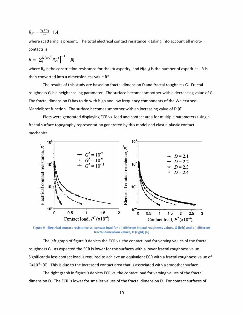
Figure 9 ‐ Electrical contact resistance vs. contact load for a.) different fractal roughness values, G (left) and b.) different fractal dimension values, D (right) [6]
The left graph of figure 9 depicts the ECR vs. the contact load for varying values of the fractal
roughness G. As expected the ECR is lower for the surfaces with a lower fractal roughness value.
Significantly less contact load is required to achieve an equivalent ECR with a fractal roughness value of
G=10‐11 [6]. This is due to the increased contact area that is associated with a smoother surface.
The right graph in figure 9 depicts ECR vs. the contact load for varying values of the fractal
dimension D. The ECR is lower for smaller values of the fractal dimension D. For contact surfaces of
11
increasing smoothness, the contact area will be greater and the ECR will be lower. The results of this
plot are similar to the variation of fractal roughness G [6].
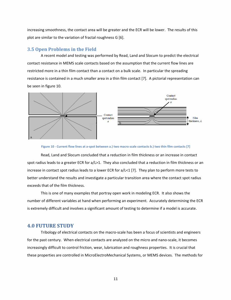
3.5OpenProblemsintheField A recent model and testing was performed by Read, Land and Slocum to predict the electrical
contact resistance in MEMS scale contacts based on the assumption that the current flow lines are
restricted more in a thin film contact than a contact on a bulk scale. In particular the spreading
resistance is contained in a much smaller area in a thin film contact [7]. A pictorial representation can
be seen in figure 10.
Figure 10 ‐ Current flow lines at a‐spot between a.) two macro scale contacts b.) two thin film contacts [7]
Read, Land and Slocum concluded that a reduction in film thickness or an increase in contact
spot radius leads to a greater ECR for a/L>1. They also concluded that a reduction in film thickness or an
increase in contact spot radius leads to a lower ECR for a/L<1 [7]. They plan to perform more tests to
better understand the results and investigate a particular transition area where the contact spot radius
exceeds that of the film thickness.
This is one of many examples that portray open work in modeling ECR. It also shows the
number of different variables at hand when performing an experiment. Accurately determining the ECR
is extremely difficult and involves a significant amount of testing to determine if a model is accurate.
4.0FUTURESTUDY Tribology of electrical contacts on the macro‐scale has been a focus of scientists and engineers
for the past century. When electrical contacts are analyzed on the micro and nano‐scale, it becomes
increasingly difficult to control friction, wear, lubrication and roughness properties. It is crucial that
these properties are controlled in MicroElectroMechanical Systems, or MEMS devices. The methods for
12
controlling friction, wear and lubrication of macro‐scale contacts do not apply to micro‐scale contacts
[3][7].
In MEMS devices, the dimensions of the contact area are on par with the system dimensions.
New tools have been developed in recent decades to cope with the drastic reduction in scale. Atomic
force microscopes, 3D contact/non‐contact profilometers and optic/untrasonic instruments are now
aiding scientists and engineers in analyzing micro and nano‐scale surfaces [2]. Advanced computer
simulations have also been developed to allow for more comprehensive analyses and visualizations of
what is actually going on at this scale. With macro‐scale contacts, one can see the system with their
eyes or a basic microscope. There is also a significant amount of history that details the study of macro‐
scale contact design principles and phenomena. Micro and nano‐scale contacts are the new frontier of
tribology and will be a key player in tribology in the coming decades.
13
REFERENCES [1] Barber, J.R. “Surface Roughness and Electrical Contact Resistance.” Weblog Entry. iMechanica, web
of mechanics and mechanicians. Jan. 10, 2007. Accessed: Nov. 27, 2011. <http://imechanica.org/node/671>
[2] Braunović, Milenko et al. , Electrical Contacts: Fundamentals, Applications and Technology. Boca
Raton: CRC Press, Taylor & Francis Group, 2007. [3] Day, Linda A. “Tribology Frontiers in Electrical Contacts.” Tribology & Lubrication Technology.
FindArticles.com. 12 Oct, 2011 <http://findarticles.com/p/articles/mi_qa5322/is_200608/ai_n21399326/pg_4/?tag=content;co
l1> [4] Greenwood, J.A. and Williamson, J.B.P. “Contact of Nominally Flat Surfaces.” Proceedings of the
Royal Society of London. Series A, Mathematical & Physical Sciences 295.1442 (1966): 300‐319. [5] Holm, Ragnar. Electrical Contacts ‐ Theory and Application. New York: Springer‐Verlag, 1967. [6] Kogut, L., Komvopoulos, K. “Electrical Contact Resistance Theory for Conductive Rough Surfaces.”
Journal of Applied Physics 94.5 (2003): 3153‐3162. [7] Read, M.B., Lang, J.H., Slocum, A.H. “Contact Resistance in Flat Thin Films.” 2009 Proceedings of the
55th IEEE Holm Conference on Electrical Contacts (2009): 300‐306. [8] Slade, Paul G., Electrical Contacts – Principles and Applications. New York: Marcel Dekker, 1999. [9] Wilson, Evertt W., Santosh Angadi, and Robert Jackson. “Electrical Contact Resistance Considering
Multi‐Scale Roughness.” 2008 Proceedings of the 54th IEEE Holm Conference on Electrical Contacts (2008): 190‐197.