Embed Size (px)
Citation preview

User's GuideSLAU253A–June 2008–Revised September 2011
Triple- and Quad-Channel Digital Isolator EVM
CAUTION
This evaluation module (EVM) is made available for isolator parameterperformance evaluation only and is not intended for isolation voltage testing. Toprevent damage to the EVM, any voltage applied as a supply or digitalinput/output must be maintained within the 0-V to 5.5-V recommendedoperating range.
Exceeding the specified input voltage range may cause unexpected operation and/or irreversible damageto the EVM. If there are questions concerning the input voltage range, contact a TI field representativeprior to connecting power.
Applying loads outside of the specified output range may result in unintended operation and/or possiblepermanent damage to the EVM. If there is uncertainty as to the load specification, contact a TI fieldrepresentative.
During normal EVM operation, case temperatures greater than 60°C may be expected. The EVM isdesigned to operate properly above 60°C as long as the input and output ranges are maintained withindata sheet specifications. When placing measurement probes near these devices during operation, beaware that these devices may be very warm to the touch.
Contents1 Introduction .................................................................................................................. 2
1.1 Overview ............................................................................................................ 21.2 The Functional Configurations of the Triple- and Quad-Channel Digital Isolator .......................... 21.3 The EVM Schematics of the Triple and Quad Isolators ....................................................... 5
2 EVM Setup and Operation ............................................................................................... 112.1 Overview ........................................................................................................... 11
List of Figures
1 The ISO7230x and ISO7231x Pinout .................................................................................... 3
2 The ISO7240CF, ISO7240x, ISO7241x, and ISO7242x Pinout ...................................................... 3
3 The EVM Top Photograph ................................................................................................. 4
4 The EVM Bottom Photograph ............................................................................................. 4
5 The ISO7230x Same-Channel Direction EVM Schematic............................................................. 5
6 The ISO7231x and ISO7631Fx Opposing-Channel Direction Schematic ........................................... 6
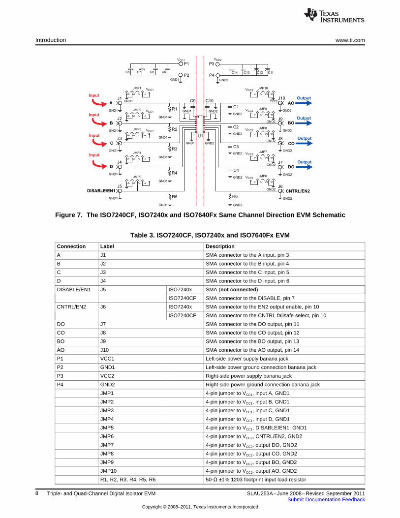
7 The ISO7240CF, ISO7240x and ISO7640Fx Same Channel Direction EVM Schematic ......................... 8
8 The ISO7241x and ISO7641Fx Single Opposing-Channel Direction Schematic................................... 9
9 The ISO7242x Dual Opposing-Channel Direction Schematic ....................................................... 10
10 Basic EVM Operation with a ISO7241C................................................................................ 12
11 Typical Output Waveforms ............................................................................................... 12
List of Tables
1 ISO7230x EVM ............................................................................................................. 5
2 ISO7231x and ISO7631Fx EVM ......................................................................................... 7
1SLAU253A–June 2008–Revised September 2011 Triple- and Quad-Channel Digital Isolator EVMSubmit Documentation Feedback
Copyright © 2008–2011, Texas Instruments Incorporated

Introduction www.ti.com
3 ISO7240CF, ISO7240x and ISO7640Fx EVM .......................................................................... 8
4 ISO7241x and ISO7641Fx EVM .......................................................................................... 9
5 ISO7242x EVM ............................................................................................................ 10
1 Introduction
This user's guide details the evaluation module (EVM) operation of a factory-installed ISO7241Cquad-channel digital isolator. However, the EVM board may be reconfigured by a user for evaluation ofany of TI's triple- or quad-channel digital isolators.
The EVM may be reconfigured for use with the ISO7230A, ISO7230C, ISO7230M, ISO7240A,ISO7240CF, ISO7240M and ISO7640Fx same-channel direction isolators as well as the ISO7231A,ISO7231C, ISO7231M, ISO7241A, ISO7241M, ISO7242A, ISO7242C, ISO7242M, ISO7631Fx andISO7641Fx opposing-channel direction isolators. Contact TI for a factory installation of any of thesedevices.
This guide also explains the user-configurable I/O loads for both triple- and quad-channel isolator EVMconfigurations and presents a typical laboratory setup with output waveforms.
1.1 Overview
The ISO723x, ISO724x, ISO763x and ISO764X digital isolators have a logic input and output bufferseparated by a silicon oxide (SiO2) insulation barrier. Used with isolated power supplies, these devicesblock high voltage, isolate grounds, and prevent noise currents on a data bus or other circuits fromentering the local ground and interfering with or damaging sensitive circuitry.
A binary input signal is conditioned, translated to a balanced signal, and then differentiated by thecapacitive isolation barrier. Across the isolation barrier, a differential comparator receives the logictransition information, then sets or resets a flip-flop and the output circuit accordingly. A periodic updatepulse is sent across the barrier to ensure the proper dc level of the output. If this dc-refresh pulse is notreceived for more than 4 µs, the input is assumed to be unpowered or not being actively driven, and afailsafe circuit drives the output to a logic-high state. For ISO7640FM, ISO7640FC, ISO7641FM,ISO7641FC, ISO7631FM and ISO7631FC failsafe is logic low state. For ISO7240CF logic low state ifselected.
CAUTION
Note that although these devices provide galvanic isolation of up to 4000 V, thisEVM cannot be used for isolation voltage testing. It is designed for theevaluation of device operating parameters only and may be damaged if highvoltage (> 5.5 V) is applied anywhere in the circuit.
1.2 The Functional Configurations of the Triple- and Quad-Channel Digital Isolator
The pinouts of the triple-channel digital isolators are displayed in Figure 1. The EVM comes with anISO7241C installed; however, a user may reconfigure this versatile EVM for use with any of the triple- orquad-channel footprints.
Not that ISO7231x and ISO7631Fx have the same pin out. As does ISO7240x with ISO7640Fx, andISO7241X with ISO7641Fx.
2 Triple- and Quad-Channel Digital Isolator EVM SLAU253A–June 2008–Revised September 2011Submit Documentation Feedback
Copyright © 2008–2011, Texas Instruments Incorporated

1
2
3
4
5
6
7
8 9
10
11
12
13
14
15
16
NC
NC
GND1
NC
GND2
GND2
OUTA
OUTC
OUTB
EN
1
2
3
4
5
6
7
8 9
10
11
12
13
14
15
16VCC1
GND1
INA
INB
INC
VCC2
EN1
NC
GND1
VCC1
GND1
INA
INB
OUTC
NC
GND2
GND2
OUTA
INC
OUTB
EN2
VCC2
ISO7230x ISO7231x
1
2
3
4
5
6
7
8 9
10
11
12
13
14
15
16V
CC1
GND1
INA
INB
INC
IND
DISABLE
GND1
VCC2
GND2
OUTA
OUTB
OUTC
OUTD
CTRL
GND2
ISO7240CF
1
2
3
4
5
6
7
8 9
10
11
12
13
14
15
16VCC1
GND1
INA
INB
INC
IND
NC
GND1
ISO7240x
VCC2
GND2
OUTA
OUTB
OUTC
OUTD
EN
GND2
VCC2
GND2
OUTA
OUTB
OUTC
IND
GND2
1
2
3
4
5
6
7
8 9
10
11
12
13
14
15
16V
CC1
GND1
INA
INB
INC
OUTD
EN1
GND1
EN2
ISO7241x
1
2
3
4
5
6
7
8 9
10
11
12
13
14
15
16VCC1
GND1
INA
INB
OUTC
OUTD
EN1
GND1
VCC2
GND2
OUTA
OUTB
INC
IND
EN2
GND2
ISO7242x
www.ti.com Introduction
Figure 1. The ISO7230x and ISO7231x Pinout
The ISO7230A, ISO7231A, ISO7230C, and ISO7231C have TTL input thresholds and an input noise-filterthat prevents transient pulses of up to 2 ns in duration from being passed to the output of the device.
The ISO7631FC has TTL input thresholds and an input noise-filter that prevents transient pulses of up to10 ns in duration from being passed to the output of the device.
The ISO7230M and ISO7231M have a CMOS Vcc/2 input threshold and do not have the noise-filter withthe additional propagation delay.
The ISO7631FM has TTL input thresholds and do not have the noise-filter or the additonal prop delay.
Figure 2. The ISO7240CF, ISO7240x, ISO7241x, and ISO7242x Pinout
The ISO7240A, ISO7240C, ISO7241A, ISO7241C, ISO7242A, and ISO7242C have TTL input thresholdsand an input noise-filter that prevents transient pulses of up to 2 ns in duration from being passed to theoutput of the device.
The ISO7640FC and ISO7641FC have TTL input thresholds and an input noise-filter that preventstransient pulses of up to 10 ns in duration from being passed to the output of the device.
The ISO7240M, ISO7241M, and ISO7242M have a CMOS Vcc/2 input threshold and do not have thenoise-filter with the additional propagation delay.
The ISO7640FM and ISO7641FM have TTL input thresholds and do not have the noise-filter or theadditonal prop delay
3SLAU253A–June 2008–Revised September 2011 Triple- and Quad-Channel Digital Isolator EVMSubmit Documentation Feedback
Copyright © 2008–2011, Texas Instruments Incorporated

Jumpers
Output
Load
Capacitors Input
Load
Resistors
Introduction www.ti.com
Figure 3. The EVM Top Photograph
The 4-pin jumpers on top of the EVM provide for an input or output pin to be tied to either Vcc or ground.The jumper also provides scope probe access to each pin.
Figure 4. The EVM Bottom Photograph
Each channel is configured with a 50-Ω load resistor on each input, labeled R1 through R4, and a 4.7-pFload on each channel output labeled C1 through C4. Note that each channel may be configured foroperation in either direction by simply switching the input load resistor with the output load capacitor.
4 Triple- and Quad-Channel Digital Isolator EVM SLAU253A–June 2008–Revised September 2011Submit Documentation Feedback
Copyright © 2008–2011, Texas Instruments Incorporated

C14 C13 C12 C11
VCC2
GND2
C5C6C7C8
GND1
1 2 3 4
JMP6
1 2 3 4JMP8
1 2 3 4
JMP91 2 3 4
JMP10
1234JMP3
1234
JMP21234
JMP1
R6
R1
R3
R2
P1 P3
P2 P4
J1
J2
J3
J4
J5 J6
J7
J8
J9
J10
C1
C2
C3
C10C9
VCC1
ISOLATION BARRIER
GND1
GND1
GND1
GND1
GND1 GND2
GND2
GND2
GND2
GND2
GND2
GND2
GND2
GND2
GND2
GND2
GND1
GND1
GND1
GND1
GND1
GND1
VCC1
VCC1
VCC1
VCC2
VCC2
VCC2
VCC2
VCC2
GND2
GND2
GND2
AO
BO
CO
DO
CNTRL/EN2
A
B
C
D
DISABLE /EN1
U1
Input
Input
Input
Output
Output
Output
www.ti.com Introduction
For example, in Figure 6, because the ISO7231 has the bottom channel configured in the opposingdirection, R3 and C3 have changed place from that in Figure 5. This is all that is required to reconfigure achannel direction.
A user may also evaluate varied input and output loading conditions by replacing the factory-installed1203 footprint loads.
1.3 The EVM Schematics of the Triple and Quad Isolators
This multifunctional EVM is designed with the signal paths displayed in Figure 1, Figure 5, and Figure 6for the evaluation of the ISO7230x, ISO7231x and ISO7631Fx triple-channel isolators.
The functional signal path schematics of the ISO7240CF, ISO7240x and ISO7640Fx are presented inFigure 2 and Figure 7, whereas the ISO7241x, ISO7641Fx and ISO7242x are displayed in Figure 2,Figure 8, and Figure 9.
Note that each input channel has a 50-Ω load resistor to ground. Each output channel has a 4.7-pF loadcapacitor to ground that when added to the parallel capacitance of the trace to the SMA connector bringsthe total capacitive load to 15 pF.
When a channel direction is reversed, the 50-Ω resistor and 4.7-pF capacitor change place, each to theother side of the isolation barrier as displayed in Figure 6 for the opposing channel.
Figure 5. The ISO7230x Same-Channel Direction EVM Schematic
Table 1. ISO7230x EVM
Connection Label Description
A J1 SMA connector to the A input, pin 3
B J2 SMA connector to the B input, pin 4
C J3 SMA connector to the C input, pin 5
D J4 SMA connector (not used)
DISABLE/EN1 J5 SMA connector (not used)
CNTRL/EN2 J6 SMA connector to the output enable input, pin 10
DO J7 SMA connector (not used)
5SLAU253A–June 2008–Revised September 2011 Triple- and Quad-Channel Digital Isolator EVMSubmit Documentation Feedback
Copyright © 2008–2011, Texas Instruments Incorporated

C14 C13 C12 C11
VCC2
GND2
C5C6C7C8
GND1
1 2 3 4
JMP6
1 2 3 4
JMP8
1 2 3 4
JMP9
1 2 3 4
JMP10
1234
JMP3
1234
JMP2
1234
JMP1
R6
R1
R2
P1 P3
P2 P4
J1
J2
J3
J4
J5 J6
J7
J8
J9
J10
C1
C2
C10C9
VCC1
ISOLATION BARRIER
GND1
GND1
GND1
GND1 GND2
GND2
GND2
GND2
GND2
GND2
GND2
GND2
GND2
GND2
GND1
GND1
GND1
GND1
GND1
GND1
VCC1
VCC1
VCC1
VCC2
VCC2
VCC2
VCC2
VCC2
GND2
GND2
GND2
AO
BO
C
DO
CNTRL/EN2
A
B
CO
D
DISABLE/EN1
C3
GND1
R3
GND2
U1
Input
Output
Input
Input
Output
Output
1234
JP5 VCC1
R5
GND1
Introduction www.ti.com
Table 1. ISO7230x EVM (continued)
Connection Label Description
CO J8 SMA connector to the CO output, pin 12
BO J9 SMA connector to the BO output, pin 13
AO J10 SMA connector to the AO output, pin 14
P1 VCC1 Left-side power supply banana jack
P2 GND1 Left-side power ground connection banana jack
P3 VCC2 Right-side power supply banana jack
P4 GND2 Right-side power ground connection banana jack
JMP1 4-pin jumper to VCC1, input A, GND1
JMP2 4-pin jumper to VCC1, input B, GND1
JMP3 4-pin jumper to VCC1, input C, GND1
JMP4 4-pin jumper (not used)
JMP5 4-pin jumper (not used)
JMP6 4-pin jumper to VCC2, EN2, GND2
JMP7 4-pin jumper (not used)
JMP8 4-pin jumper to VCC2, output CO, GND2
JMP9 4-pin jumper to VCC2, output BO, GND2
JMP10 4-pin jumper to VCC2, output AO, GND2
R1, R2, R3, R4, R5, R6 50\-Ω ±1% 1203 footprint input load resistor
C1, C2, C3, C4 4.7-pF 1203 footprint output load capacitor
C5, C11 0.1-μF filter capacitor
C6, C12 1.0-μF filter capacitor
C7, C13 10-μF electrolytic filter capacitor
C8, C14 68-μF electrolytic filter capacitor
C9, C10 0.01-μF filter capacitor
R7, R8, R9, R10, R11, R12 open, not populated
Figure 6. The ISO7231x and ISO7631Fx Opposing-Channel Direction Schematic
6 Triple- and Quad-Channel Digital Isolator EVM SLAU253A–June 2008–Revised September 2011Submit Documentation Feedback
Copyright © 2008–2011, Texas Instruments Incorporated

www.ti.com Introduction
Table 2. ISO7231x and ISO7631Fx EVM
Connection Label Description
A J1 SMA connector to the A input, pin 3
B J2 SMA connector to the B input, pin 4
CO J3 SMA connector to the C0 output, pin 5
D J4 SMA connector (not used)
DISABLE/EN1 J5 SMA connector to the EN1 output enable, pin 7
CNTRL/EN2 J6 SMA connector to the EN2 output enable, pin 10
DO J7 SMA connector (not used)
C J8 SMA connector to the C input, pin 12
BO J9 SMA connector to the BO output, pin 13
AO J10 SMA connector to the AO output, pin 14
P1 VCC1 Left-side power supply banana jack
P2 GND1 Left-side power ground connection banana jack
P3 VCC2 Right-side power supply banana jack
P4 GND2 Right-side power ground connection banana jack
JMP1 4-pin jumper to VCC1, input A, GND1
JMP2 4-pin jumper to VCC1, input B, GND1
JMP3 4-pin jumper – VCC1, output CO, GND1
JMP4 4-pin jumper (not used)
JMP5 4-pin jumper to VCC1, EN1, GND1
JMP6 4-pin jumper to VCC2, EN2, GND2
JMP7 4-pin jumper (not used)
JMP8 4-pin jumper to VCC2, input C, GND2
JMP9 4-pin jumper to VCC2, output BO, GND2
JMP10 4-pin jumper to VCC2, output AO, GND2
R1, R2, R3, R4, R5, R6 50-Ω ±1% 1203 footprint input load resistor
C1, C2, C3, C4 4.7-pF 1203 footprint output load capacitor
C5, C11 0.1-μF filter capacitor
C6, C12 1-μF filter capacitor
C7, C13 10-μF electrolytic filter capacitor
C8, C14 68-μF electrolytic filter capacitor
C9, C10 0.01-μF filter capacitor
R7, R8, R9, R10, R11, R12 open, not populated
7SLAU253A–June 2008–Revised September 2011 Triple- and Quad-Channel Digital Isolator EVMSubmit Documentation Feedback
Copyright © 2008–2011, Texas Instruments Incorporated
C14 C13 C12 C11
VCC2
GND2
C5C6C7C8
GND1
1 2 3 4
JMP6
1 2 3 4
JMP8
1 2 3 4
JMP9
1 2 3 4
JMP10
1234
JMP3
1234
JMP2
1234
JMP1
R6
R1
R3
R2
P1 P3
P2 P4
J1
J2
J3
J4
J5 J6
J7
J8
J9
J10
C1
C2
C3
C10C9
VCC1
GND1
GND1
GND1
GND1
GND1 GND2
GND2
GND2
GND2
GND2
GND2
GND2
GND2
GND2
GND2
GND2
GND1
GND1
GND1
GND1
GND1
GND1
VCC1
VCC1
VCC1
VCC2
VCC2
VCC2
VCC2
VCC2
GND2
GND2
GND2
AO
BO
CO
DO
CNTRL/EN2
A
B
C
D
DISABLE/EN1
U1
R4
GND1
1234
JMP4
C4
GND2
1 2 3 4
JMP7VCC2
GND2
1234
JMP5
Output
Output
Output
Output
Input
Input
Input
Input
R5
GND1
Introduction www.ti.com
Figure 7. The ISO7240CF, ISO7240x and ISO7640Fx Same Channel Direction EVM Schematic
Table 3. ISO7240CF, ISO7240x and ISO7640Fx EVM
Connection Label Description
A J1 SMA connector to the A input, pin 3
B J2 SMA connector to the B input, pin 4
C J3 SMA connector to the C input, pin 5
D J4 SMA connector to the D input, pin 6
DISABLE/EN1 J5 ISO7240x SMA (not connected)
ISO7240CF SMA connector to the DISABLE, pin 7
CNTRL/EN2 J6 ISO7240x SMA connector to the EN2 output enable, pin 10
ISO7240CF SMA connector to the CNTRL failsafe select, pin 10
DO J7 SMA connector to the DO output, pin 11
CO J8 SMA connector to the CO output, pin 12
BO J9 SMA connector to the BO output, pin 13
AO J10 SMA connector to the AO output, pin 14
P1 VCC1 Left-side power supply banana jack
P2 GND1 Left-side power ground connection banana jack
P3 VCC2 Right-side power supply banana jack
P4 GND2 Right-side power ground connection banana jack
JMP1 4-pin jumper to VCC1, input A, GND1
JMP2 4-pin jumper to VCC1, input B, GND1
JMP3 4-pin jumper to VCC1, input C, GND1
JMP4 4-pin jumper to VCC1, input D, GND1
JMP5 4-pin jumper to VCC1, DISABLE/EN1, GND1
JMP6 4-pin jumper to VCC2, CNTRL/EN2, GND2
JMP7 4-pin jumper to VCC2, output DO, GND2
JMP8 4-pin jumper to VCC2, output CO, GND2
JMP9 4-pin jumper to VCC2, output BO, GND2
JMP10 4-pin jumper to VCC2, output AO, GND2
R1, R2, R3, R4, R5, R6 50-Ω ±1% 1203 footprint input load resistor
8 Triple- and Quad-Channel Digital Isolator EVM SLAU253A–June 2008–Revised September 2011Submit Documentation Feedback
Copyright © 2008–2011, Texas Instruments Incorporated

C14 C13 C12 C11
VCC2
GND2
C5C6C7C8
GND1
1 2 3 4
JMP6
1 2 3 4
JMP8
1 2 3 4
JMP9
1 2 3 4
JMP10
1234
JMP3
1234
JMP2
1234
JMP1
R6
R1
R3
R2
P1 P3
P2 P4
J1
J2
J3
J4
J5 J6
J7
J8
J9
J10
C1
C2
C3
C10C9
VCC1
GND1
GND1
GND1
GND1
GND1 GND2
GND2
GND2
GND2
GND2
GND2
GND2
GND2
GND2
GND2
GND2
GND1
GND1
GND1
GND1
GND1
GND1
VCC1
VCC1
VCC1
VCC2
VCC2
VCC2
VCC2
VCC2
GND2
GND2
GND2
AO
BO
CO
DO
CNTRL/EN2
A
B
C
D
DISABLE/EN1
U1
GND1
1234
JMP4
GND2
1 2 3 4
JMP7VCC2
GND21234
JMP5
R4C4
Input
Input
Output
Input
Input
Output
Output
Output
R5
GND1
www.ti.com Introduction
Table 3. ISO7240CF, ISO7240x and ISO7640Fx EVM (continued)
Connection Label Description
C1, C2, C3, C4 4.7-pF 1203 footprint load capacitor
C5, C11 0.1-μF filter capacitor
C6, C12 1- μF filter capacitor
C7, C13 10-μF electrolytic filter capacitor
C8, C14 68-μF electrolytic filter capacitor
C9, C10 0.01- μF filter capacitor
R7, R8, R9, R10, R11, R12 open, not populated
Figure 8. The ISO7241x and ISO7641Fx Single Opposing-Channel Direction Schematic
Table 4. ISO7241x and ISO7641Fx EVM
Connection Label Description
A J1 SMA connector to the A input, pin 3
B J2 SMA connector to the B input, pin 4
C J3 SMA connector to the C input, pin 5
DO J4 SMA connector to the DO output, pin 6
DISABLE/EN1 J5 SMA connector to the EN1 output enable, pin 7
CNTRL/EN2 J6 SMA connector to the EN2 output enable, pin 10
D J7 SMA connector to the D input, pin 11
CO J8 SMA connector to the CO output, pin 12
BO J9 SMA connector to the BO output, pin 13
AO J10 SMA connector to the AO output, pin 14
P1 VCC1 Left-side power supply banana jack
P2 GND1 Left-side power ground connection banana jack
P3 VCC2 Right-side power supply banana jack
P4 GND2 Right-side power ground connection banana jack
JMP1 4-pin jumper to VCC1, input A, GND1
JMP2 4-pin jumper to VCC1, input B, GND1
9SLAU253A–June 2008–Revised September 2011 Triple- and Quad-Channel Digital Isolator EVMSubmit Documentation Feedback
Copyright © 2008–2011, Texas Instruments Incorporated

C14 C13 C12 C11
VCC2
GND2
C5C6C7C8
GND1
1 2 3 4
JMP6
1 2 3 4
JMP8
1 2 3 4
JMP9
1 2 3 4
JMP101234
JMP3
1234
JMP2
1234
JMP1
R6
R1
R2
P1 P3
P2 P4
J1
J2
J3
J4
J5 J6
J7
J8
J9
J10
C1
C2
C10C9
VCC1
GND1
GND1
GND1
GND1
GND1 GND2
GND2
GND2
GND2
GND2
GND2
GND2
GND2
GND2
GND2
GND2
GND1
GND1
GND1
GND1
GND1
GND1
VCC1
VCC1
VCC1
VCC2
VCC2
VCC2
VCC2
VCC2
GND2
GND2
GND2
AO
BO
CO
DO
CNTRL/EN2
A
B
C
D
DISABLE/EN1
U1
GND1
1234
JMP4
GND2
1 2 3 4
JMP7VCC2
GND2
1234
JMP5
R4C4
R3C3
Input
Input
Input
Input
Output
Output
Output
Output
R5
GND1
Introduction www.ti.com
Table 4. ISO7241x and ISO7641Fx EVM (continued)
Connection Label Description
JMP3 4-pin jumper – VCC1, input C, GND1
JMP4 4-pin jumper – VCC1, output DO, GND1
JMP5 4-pin jumper – VCC1, EN1, GND1
JMP6 4-pin jumper to VCC2, EN2, GND2
JMP7 4-pin jumper – VCC2, input D, GND2
JMP8 4-pin jumper – VCC2, output CO, GND2
JMP9 4-pin jumper to VCC2, output BO, GND2
JMP10 4-pin jumper to VCC2, output AO, GND2
R1, R2, R3, R4, R5, R6 50-Ω ±1% 1203 footprint input load resistor
C1, C2, C3, C4 4.7-pF 1203 footprint output load capacitor
C5, C11 0.1-μF filter capacitor
C6, C12 1- μF filter capacitor
C7, C13 10-μF electrolytic filter capacitor
C8, C14 68-μF electrolytic filter capacitor
C9, C10 0.01-μF filter capacitor
R7, R8, R9, R10, R11, R12 open, not populated
Figure 9. The ISO7242x Dual Opposing-Channel Direction Schematic
Table 5. ISO7242x EVM
Connection Label Description
A J1 SMA connector to the A input, pin 3
B J2 SMA connector to the B input, pin 4
CO J3 SMA connector to the CO output, pin 5
DO J4 SMA connector to the DO output, pin 6
DISABLE/EN1 J5 SMA connector to the EN1 output enable, pin 7
CNTRL/EN2 J6 SMA connector to the EN2 output enable, pin 10
D J7 SMA connector to the D input, pin 11
10 Triple- and Quad-Channel Digital Isolator EVM SLAU253A–June 2008–Revised September 2011Submit Documentation Feedback
Copyright © 2008–2011, Texas Instruments Incorporated

www.ti.com EVM Setup and Operation
Table 5. ISO7242x EVM (continued)
Connection Label Description
C J8 SMA connector to the C input, pin 12
BO J9 SMA connector to the BO output, pin 13
AO J10 SMA connector to the AO output, pin 14
P1 VCC1 Left-side power supply banana jack
P2 GND1 Left-side power ground connection banana jack
P3 VCC2 Right-side power supply banana jack
P4 GND2 Right-side power ground connection banana jack
JMP1 4-pin jumper to VCC1, input A, GND1
JMP2 4-pin jumper to VCC1, input B, GND1
JMP3 4-pin jumper – VCC1, output CO, GND1
JMP4 4-pin jumper – VCC1, output DO, GND1
JMP5 4-pin jumper – VCC1, EN1, GND1
JMP6 4-pin jumper to VCC2, EN2, GND2
JMP7 4-pin jumper – VCC2, input D, GND2
JMP8 4-pin jumper – VCC2, input C, GND2
JMP9 4-pin jumper to VCC2, output B, GND2
JMP10 4-pin jumper to VCC2, output A, GND2
R1, R2, R3, R4, R5, R6 50-Ω ±1% 1203 footprint input load resistor
C1, C2, C3, C4 4.7-pF 1203 footprint output load capacitor
C5, C11 0.1-μF filter capacitor
C6, C12 1-μF filter capacitor
C7, C13 10-μF electrolytic filter capacitor
C8, C14 68-μF electrolytic filter capacitor
C9, C10 0.01-μF filter capacitor
R7, R8, R9, R10, R11, R12 open, not populated
2 EVM Setup and Operation
This section includes the setup and operation of the EVM for parameter performance evaluation. Typicaloutput waveforms are included
2.1 Overview
The basic setup in Figure 10 has the two power supplies required to evaluate isolator performance withany combination of 3.3
V or 5
V on either side. If both sides are to be evaluated at the same supply voltage, only one power supply isrequired and can be used to power both sides of the EVM.
CAUTION
Note that this EVM is for operating parameter performance evaluation only andnot designed for isolation voltage testing. Any voltage applied above the 5.5-Vmaximum recommended operating voltage of the isolators will damage theEVM.
11SLAU253A–June 2008–Revised September 2011 Triple- and Quad-Channel Digital Isolator EVMSubmit Documentation Feedback
Copyright © 2008–2011, Texas Instruments Incorporated
P1 P 3P2 P4
Power Supply Power Supply
Tektronix
HFS9009
PatternGenerator
Tektronix
784D
Scope
VCC1 GND2GND1INPUT
OUTPUT
OUTPUT
AINPUT
VCC2
B
C
D
DISABLE/EN1 CNTRL/EN2
AO
BO
CO
DOINPUT
OUTPUTINPUT
OUTPUT
EVM Setup and Operation www.ti.com
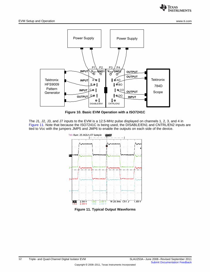
Figure 10. Basic EVM Operation with a ISO7241C
The J1, J2, J3, and J7 inputs to the EVM is a 12.5-MHz pulse displayed on channels 1, 2, 3, and 4 inFigure 11. Note that because the ISO7241C is being used, the DISABLE/EN1 and CNTRL/EN2 inputs aretied to Vcc with the jumpers JMP5 and JMP6 to enable the outputs on each side of the device.
Figure 11. Typical Output Waveforms
12 Triple- and Quad-Channel Digital Isolator EVM SLAU253A–June 2008–Revised September 2011Submit Documentation Feedback
Copyright © 2008–2011, Texas Instruments Incorporated

Evaluation Board/Kit Important Notice
Texas Instruments (TI) provides the enclosed product(s) under the following conditions:
This evaluation board/kit is intended for use for ENGINEERING DEVELOPMENT, DEMONSTRATION, OR EVALUATIONPURPOSES ONLY and is not considered by TI to be a finished end-product fit for general consumer use. Persons handling theproduct(s) must have electronics training and observe good engineering practice standards. As such, the goods being provided arenot intended to be complete in terms of required design-, marketing-, and/or manufacturing-related protective considerations,including product safety and environmental measures typically found in end products that incorporate such semiconductorcomponents or circuit boards. This evaluation board/kit does not fall within the scope of the European Union directives regardingelectromagnetic compatibility, restricted substances (RoHS), recycling (WEEE), FCC, CE or UL, and therefore may not meet thetechnical requirements of these directives or other related directives.
Should this evaluation board/kit not meet the specifications indicated in the User’s Guide, the board/kit may be returned within 30days from the date of delivery for a full refund. THE FOREGOING WARRANTY IS THE EXCLUSIVE WARRANTY MADE BYSELLER TO BUYER AND IS IN LIEU OF ALL OTHER WARRANTIES, EXPRESSED, IMPLIED, OR STATUTORY, INCLUDINGANY WARRANTY OF MERCHANTABILITY OR FITNESS FOR ANY PARTICULAR PURPOSE.
The user assumes all responsibility and liability for proper and safe handling of the goods. Further, the user indemnifies TI from allclaims arising from the handling or use of the goods. Due to the open construction of the product, it is the user’s responsibility totake any and all appropriate precautions with regard to electrostatic discharge.
EXCEPT TO THE EXTENT OF THE INDEMNITY SET FORTH ABOVE, NEITHER PARTY SHALL BE LIABLE TO THE OTHERFOR ANY INDIRECT, SPECIAL, INCIDENTAL, OR CONSEQUENTIAL DAMAGES.
TI currently deals with a variety of customers for products, and therefore our arrangement with the user is not exclusive.
TI assumes no liability for applications assistance, customer product design, software performance, or infringement ofpatents or services described herein.
Please read the User’s Guide and, specifically, the Warnings and Restrictions notice in the User’s Guide prior to handling theproduct. This notice contains important safety information about temperatures and voltages. For additional information on TI’senvironmental and/or safety programs, please contact the TI application engineer or visit www.ti.com/esh.
No license is granted under any patent right or other intellectual property right of TI covering or relating to any machine, process, orcombination in which such TI products or services might be or are used.
FCC Warning
This evaluation board/kit is intended for use for ENGINEERING DEVELOPMENT, DEMONSTRATION, OR EVALUATIONPURPOSES ONLY and is not considered by TI to be a finished end-product fit for general consumer use. It generates, uses, andcan radiate radio frequency energy and has not been tested for compliance with the limits of computing devices pursuant to part 15of FCC rules, which are designed to provide reasonable protection against radio frequency interference. Operation of thisequipment in other environments may cause interference with radio communications, in which case the user at his own expensewill be required to take whatever measures may be required to correct this interference.
EVM Warnings and Restrictions
It is important to operate this EVM within the input voltage range of 0 V to 5.5 V and the output voltage range of 0 V to 5.5 V .
Exceeding the specified input range may cause unexpected operation and/or irreversible damage to the EVM. If there arequestions concerning the input range, please contact a TI field representative prior to connecting the input power.
Applying loads outside of the specified output range may result in unintended operation and/or possible permanent damage to theEVM. Please consult the EVM User's Guide prior to connecting any load to the EVM output. If there is uncertainty as to the loadspecification, please contact a TI field representative.
During normal operation, some circuit components may have case temperatures greater than 60°C. The EVM is designed tooperate properly with certain components above 60°C as long as the input and output ranges are maintained. These componentsinclude but are not limited to linear regulators, switching transistors, pass transistors, and current sense resistors. These types ofdevices can be identified using the EVM schematic located in the EVM User's Guide. When placing measurement probes nearthese devices during operation, please be aware that these devices may be very warm to the touch.
Mailing Address: Texas Instruments, Post Office Box 655303, Dallas, Texas 75265Copyright © 2011, Texas Instruments Incorporated

IMPORTANT NOTICE
Texas Instruments Incorporated and its subsidiaries (TI) reserve the right to make corrections, modifications, enhancements, improvements,and other changes to its products and services at any time and to discontinue any product or service without notice. Customers shouldobtain the latest relevant information before placing orders and should verify that such information is current and complete. All products aresold subject to TI’s terms and conditions of sale supplied at the time of order acknowledgment.
TI warrants performance of its hardware products to the specifications applicable at the time of sale in accordance with TI’s standardwarranty. Testing and other quality control techniques are used to the extent TI deems necessary to support this warranty. Except wheremandated by government requirements, testing of all parameters of each product is not necessarily performed.
TI assumes no liability for applications assistance or customer product design. Customers are responsible for their products andapplications using TI components. To minimize the risks associated with customer products and applications, customers should provideadequate design and operating safeguards.
TI does not warrant or represent that any license, either express or implied, is granted under any TI patent right, copyright, mask work right,or other TI intellectual property right relating to any combination, machine, or process in which TI products or services are used. Informationpublished by TI regarding third-party products or services does not constitute a license from TI to use such products or services or awarranty or endorsement thereof. Use of such information may require a license from a third party under the patents or other intellectualproperty of the third party, or a license from TI under the patents or other intellectual property of TI.
Reproduction of TI information in TI data books or data sheets is permissible only if reproduction is without alteration and is accompaniedby all associated warranties, conditions, limitations, and notices. Reproduction of this information with alteration is an unfair and deceptivebusiness practice. TI is not responsible or liable for such altered documentation. Information of third parties may be subject to additionalrestrictions.
Resale of TI products or services with statements different from or beyond the parameters stated by TI for that product or service voids allexpress and any implied warranties for the associated TI product or service and is an unfair and deceptive business practice. TI is notresponsible or liable for any such statements.
TI products are not authorized for use in safety-critical applications (such as life support) where a failure of the TI product would reasonablybe expected to cause severe personal injury or death, unless officers of the parties have executed an agreement specifically governingsuch use. Buyers represent that they have all necessary expertise in the safety and regulatory ramifications of their applications, andacknowledge and agree that they are solely responsible for all legal, regulatory and safety-related requirements concerning their productsand any use of TI products in such safety-critical applications, notwithstanding any applications-related information or support that may beprovided by TI. Further, Buyers must fully indemnify TI and its representatives against any damages arising out of the use of TI products insuch safety-critical applications.
TI products are neither designed nor intended for use in military/aerospace applications or environments unless the TI products arespecifically designated by TI as military-grade or "enhanced plastic." Only products designated by TI as military-grade meet militaryspecifications. Buyers acknowledge and agree that any such use of TI products which TI has not designated as military-grade is solely atthe Buyer's risk, and that they are solely responsible for compliance with all legal and regulatory requirements in connection with such use.
TI products are neither designed nor intended for use in automotive applications or environments unless the specific TI products aredesignated by TI as compliant with ISO/TS 16949 requirements. Buyers acknowledge and agree that, if they use any non-designatedproducts in automotive applications, TI will not be responsible for any failure to meet such requirements.
Following are URLs where you can obtain information on other Texas Instruments products and application solutions:
Products Applications
Audio www.ti.com/audio Communications and Telecom www.ti.com/communications
Amplifiers amplifier.ti.com Computers and Peripherals www.ti.com/computers
Data Converters dataconverter.ti.com Consumer Electronics www.ti.com/consumer-apps
DLP® Products www.dlp.com Energy and Lighting www.ti.com/energy
DSP dsp.ti.com Industrial www.ti.com/industrial
Clocks and Timers www.ti.com/clocks Medical www.ti.com/medical
Interface interface.ti.com Security www.ti.com/security
Logic logic.ti.com Space, Avionics and Defense www.ti.com/space-avionics-defense
Power Mgmt power.ti.com Transportation and Automotive www.ti.com/automotive
Microcontrollers microcontroller.ti.com Video and Imaging www.ti.com/video
RFID www.ti-rfid.com
OMAP Mobile Processors www.ti.com/omap
Wireless Connctivity www.ti.com/wirelessconnectivity
TI E2E Community Home Page e2e.ti.com
Mailing Address: Texas Instruments, Post Office Box 655303, Dallas, Texas 75265Copyright © 2011, Texas Instruments Incorporated