Embed Size (px)
Citation preview
TRIPLE OUTPUT POWER SUPPLY
MODELS 6236B AND 6237B
OPERATING AND SERVICE MANUAL FOR:MODEL 6236B, SERIALS 1705A-00101 AND ABOVEMODEL 6237B, SERIALS 1706A-00101 AND ABOVE
* For instruments with serial numbers above those listed, a changepage may be included. Refer to Appendix A for manual back-dating changes applying to Model 6236A and 6237 A supplies.
Hewlett-Packard
HP Part No. 5950-1782 Printed: February 1977.
SECTION IGENERAL INFORMATION
1-1 INTRODUCTION
1-2 This manual covers two triple output power supplymodels, the 6236B and 6237B. Both models are com-pact general purpose bench supplies that are particularlyuseful for powering developmental IC circuits, both linearand digital. Unless one model or the other is specificallyidentified, all information in this manual applies to boththe 6236B and the 6237B.
——— CAUTION ———
Carefully read Sections II and III of thismanual before attempting to operate thepower supply.
1-3 DESCRIPTION
1-4 These constant-voltage/current-limiting tripleoutput supplies combine two 0 to ±20V tracking outputsrated at 0.5 amps with an additional single output that inthe Model 6236B is rated at 0 to+6 volts and up to 2.5amps, and in the Model 6237B is rated at 0 to +18 voltsand 1 amps. The +20V and -20V tracking outputs canalso be used in series as a single 0 to 40V 0.5-amp output.Connections to the supply's output and to chassis groundare made to binding posts on the front panel. The supply'sthree outputs share a common output terminal, which isisolated from chassis ground so that anyone output term-inal can be grounded.
1-5 All outputs are protected against overload andshort-circuit damage.The+18V output in the 6237B andthe ±20V outputs in both models are protected by circuitsthat limit the output current to 110% of its nominal maxi-mum.The overload protection circuit for the +6V outputin the 6236B has a current foldback characteristic thatreduces the output current as an overload increases untilonly 1 amp flows through a short circuit. The 6V output'scurrent limit depends on the output terminal voltage andvaries linearly between 2.75 amps at 6 volts and 1 ampat zero volts.
1-6 All controls, meters, and output terminals are
located on the front panel. One voltage control sets the0 to+6V (or+18V) output and another sets the voltagesof the 0 to +20V and 0 to -20V outputs simultaneously.These dual tracking outputs are made more versatile by theprovision of a tracking ratio control in addition to the usualvoltage control. With the tracking ratio control turned fullyclockwise to its "fixed" position, the dual outputs have afixed 1:1 tracking ratio. As the ±20V voltage control isadjusted, the voltage of the negative supply tracks the posi-tive output within ±1%. Turning the tracking ratio controlaway from its fully-clockwise position switches the dualtracking outputs into a variable tracking ratio mode. In thismode the voltage of the negative output can be set lowerthan that of the positive output. The tracking ratio controlallows the negative supply's output to be set to any valuebetween a maximum that is within 10% of the positivesupply's output and a minimum that is less than 0.5 volts.Once a ratio is established by the tracking ratio control, theratio of the positive output voltage to the negative outputvoltage remains constant as the ±20V voltage controlvaries the 0 to+20V output over its range.
1-7 The front panel also contains a line switch and apilot light, a voltmeter and an ammeter, and a meterswitch that selects one of the supply's three outputs to bemonitored on both dual-range meters.
1-8 In addition to the standard 104-to-127Vac 47-to-63Hz input, three other line voltage options are available fornominal inputs of 100, 220, and 240Vac. The supply isfurnished with a permanently attached 5-foot 3-wire ground-ing type line cord. The ac line fuse is in an extractor typefuseholder on the rear heatsink.
1-9 SPECIFICATIONS
1-10 Table 1-1 lists detailed specifications for thepower supply.
1-11 OPTIONS
1-12 Options are factory modifications of a standardinstrument that are requested by the customer. The follow-ing options are available for the instruments covered bythis manual.
1-1
OPTION NO. DESCRIPTION
100 Input Power: 87-106Vac,47-63Hz,single-phase.
Input Power: 191-233Vac,47-63Hz,single-phase.
Input Power: 208-250Vac,47-63Hz,single-phase.
One additional operating and servicemanual shipped with the power supply.
220
240
910
1-13 Before the supply is shipped from the factory, aninternalline voltage selector switch is set and the properfuse installed for the line voltage specified on the order. Alabel on the rear heatsink identifies this line voltage option.
——— CAUTION ———
Before applying power to the supply, make certainthat its line voltage selector switch (S3) is set forthe line voltage to be used. (See CAUTION noticein paragraph 3-2 for additional information.)
The user can convert an instrument from one linevoltage option to another by following the instructionsin paragraph 3-4.
1-14 ACCESSORIES
1-15 The accessories listed below may be orderedfrom your local Hewlett-Packard field sales office eitherwith the power supply or separately. (Refer to the list atthe rear of the manual for addresses.)
HP PART NO. DESCRIPTION
14513A Rack Mounting Kit for mounting one3 1/2" high supply in a standard 19"relay rack.
14523A Rack Mounting Kit for mounting two3 1/2" high supplies side by side in astandard 19" relay rack.
NOTE
Table 1-1. Specifications, Model 6236B and 6237B
Specifications apply to both modelsunless otherwise indicated.
INPUT POWER:Standard: 104-127Vac (120Vac nominal), 47-63Hz,single-phase, 112W, 140VA (Other line voltageoptions are listed in paragraph 1-12).
DC OUTPUT AND OVERLOAD PROTECTION:0 to ±20V Outputs: Maximum rated output current is0.5A. Short circuit output current is 0.55A ±5% and afixed current limit circuit limits the output of each supplyto this maximum at any output voltage setting. Unbal-anced loads within current rating are permitted.(Switching to the variable tracking ratio mode allowsthe -20V output to be varied from less than -0.5V towithin ±10% of the voltage setting of the +20V output.)
Model 6236B0 to +6V Output: Maximum rated output current is 2.5A
at 6V. The maximum available output current decreaseswith the output voltage setting. A current foldback circuitlimits the output to 2.75A ±5% at 6 volts and, withdecreasing voltage, reduces the current limit linearly to 1A±15% at zero volts (short circuited).
Model 6237 B0 to +18V Output: Maximum rated output current is
1.0A. Short circuit output current is 1.1A ±5% and a fixedcurrent limit circuit limits the output to this maximum atany output voltage setting.
TRACKING ACCURACY:The +20V and -20V outputs track within 1% with theTRACKING RATIO control in the FIXED position.
LOAD EFFECT (Load Regulation):All Outputs: Less than 0.01% plus 2mV for a full load
to no load change in output current.
SOURCE EFFECT (Line Regulation):All Outputs: Less than 0.01% plus 2mV for any line
voltage change within rating.
PARD (Ripple and Noise):All Outputs: Less than 0.35mV rms and 1.5mV p-p
(20 Hz to 20 MHz).
DRIFT (Stability):All Outputs: Less than 0.1% plus 5mV (dc to 20Hz)
during 8 hours at constant line, load, and ambient afteran initial warm-up time of 30 minutes.
1-2
1-16 INSTRUMENT AND MANUALIDENTIFICATION
1-17 Hewlett-Packard power supplies are identified bya two part serial number. The first part is the serial numberprefix, a number-letter combination that denotes the dateof a significant design change and the country of manufac-ture. The first two digits indicate the year (10 = 1970,11= 1971, etc.) the second two digits indicate the week,and the letter "A" designates the U.S.A. as the country ofmanufacture. The second part is the power supply serialnumber. A different sequential number is assigned to eachpower supply, starting with 00101.
1-18 If the serial number on your instrument does notagree with those on the title page of the manual, ChangeSheets supplied with the manual or Manual BackdatingChanges define the difference between your instrumentand the instrument described by this manual.
1-19 ORDERING ADDITIONAL MANUALS
1-20 One manual is shipped with each power supplyunless Option 910 is ordered for each extra manual. Addi-tional manuals may be purchased from your local Hewlett-Packard field office (see the list at the rear of this manualfor addresses). Specify the model number, serial numberprefix, and the HP Part Number provided on the title page.
Table 1-1. Specifications, Models 6236B and 6237B (Continued)
LOAD EFFECT TRANSIENT RECOVERY TIME:All Outputs: Less than 50µsec for output recovery to
within 15mV of nominal output voltage following a loadchange from full load to half load (or vice versa).
OUTPUT VOLTAGEOVERSHOOT:All Outputs: During turn-on or turn-off of ac power,
output plus overshoot will not exceed 1 V if the outputcontrol is set for less than 1V. If the control is set for 1Vor higher, there is no overshoot.
TEMPERATURE COEFFICIENT:All Outputs: Less than 0.02% plus 1 mV voltage
change per degree Celsius over the operating range from0 to 40°C after 30 minutes warm-up.
*OUTPUT IMPEDANCE (typical):0 to +20V Output: 0.5mΩ plus 1.5µH0 to -20V Output: 0.5mΩ plus 1.5µH
Model 6236B0 to +6V Output: 0.3mΩ plus 1µH
Model 6237B0 to +18V Output: 0.3Ω plus 1.5µH
* Operating characteristics listed as typical are providedfor the user's information only and are not warranteedspecifications.
METER ACCURACY:±4% of full scale
RESOLUTION:(Minimum output voltage change obtainable using front
panel voltage control)0 to ±20V Outputs: 70mVModel 6236B0 to +6V Output: 20mV
Model 6237B0 to +18V Output: 70mV
TEMPERATURE RATINGS:Operating: 0 to +40°C ambient. At higher
temperatures, output current is derated linearly to 50% at55°C maximum temperature.
Storage:-40°C to+75 °C.
METER RANGES:0 to +20V Output: 0-25V, 0-0.6A0 to -20V Output: 0-25V, 0-0.6A
Model 6236B0 to +6V Output: 0-7V, 0-3A
Model 6237B0 to +18V Output: 0-21V, 0-1.2A
DIMENSIONS:3.47 in. H x 8.22 in. W x 12.56 in. D(88mm H x 209mm W x 319mm D)
WEIGHT:9.5 lb (4.3kg)
1-3
SECTION IIINSTALLATION
2-2 Before shipment, this instrument was inspectedand found to be free of mechanical and electrical defects.As soon as the instrument is unpacked, inspect for anydamage that may have occurred in transit. Save all packingmaterials until the inspection is completed. If damage isfound, file claim with carrier immediately. The Hewlett-Packard Sales and Service office should be notified as soonas possible.
2-4 This check should confirm that there are no brokenknobs or connectors, that the cabinet and panel surfacesare free of dents and scratches, and that the meter is notscratched or cracked.
2-6 The instrument should be checked against its electrical specifications. Section V includes an "in-cabinet" per-formance check to verify proper instrument operation.
2-8 The instrument is shipped ready for benchoperation. Before applying power to the instrument, seethe CAUTION notice in paragraph 3-2.
2-10 This instrument is air cooled. Sufficient spaceshould be allotted so that a free flow of cooling air canreach the rear of the instrument when it is in operation. Itshould be used in an area where the ambient temperaturedoes not exceed 40°C (up to 55°C with derating).
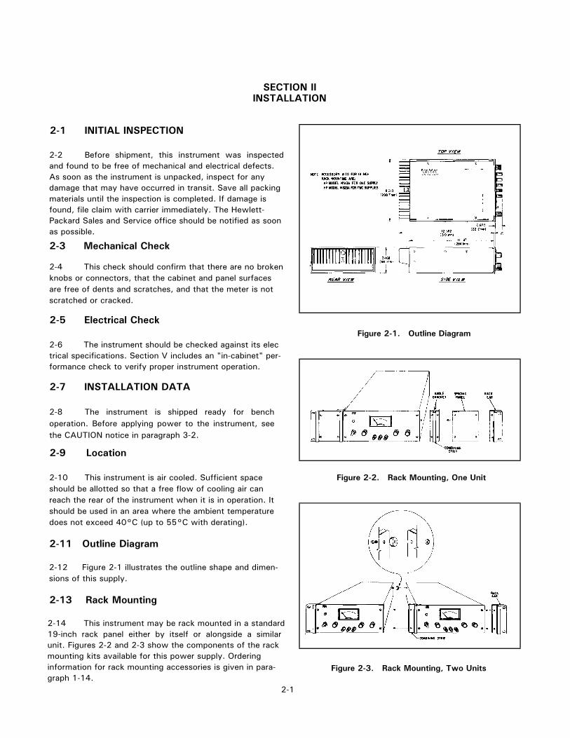
2-12 Figure 2-1 illustrates the outline shape and dimen-sions of this supply.
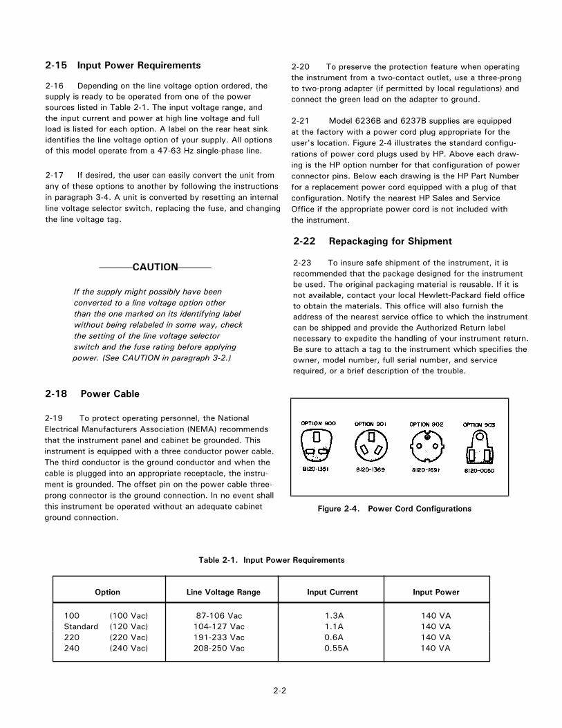
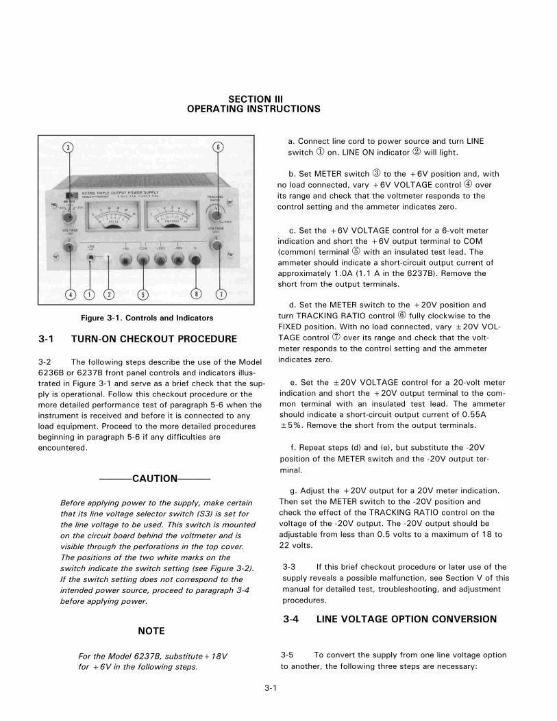
2-14 This instrument may be rack mounted in a standard19-inch rack panel either by itself or alongside a similarunit. Figures 2-2 and 2-3 show the components of the rackmounting kits available for this power supply. Orderinginformation for rack mounting accessories is given in para-graph 1-14.
2-1
2-1 INITIAL INSPECTION
2-3 Mechanical Check
2-5 Electrical Check
2-7 INSTALLATION DATA
2-9 Location
2-11 Outline Diagram
2-13 Rack Mounting
Figure 2-3. Rack Mounting, Two Units
Figure 2-2. Rack Mounting, One Unit
Figure 2-1. Outline Diagram
2-16 Depending on the line voltage option ordered, thesupply is ready to be operated from one of the powersources listed in Table 2-1. The input voltage range, andthe input current and power at high line voltage and fullload is listed for each option. A label on the rear heat sinkidentifies the line voltage option of your supply. All optionsof this model operate from a 47-63 Hz single-phase line.
2-17 If desired, the user can easily convert the unit fromany of these options to another by following the instructionsin paragraph 3-4. A unit is converted by resetting an internalline voltage selector switch, replacing the fuse, and changingthe line voltage tag.
———CAUTION———
If the supply might possibly have beenconverted to a line voltage option otherthan the one marked on its identifying labelwithout being relabeled in some way, checkthe setting of the line voltage selectorswitch and the fuse rating before applyingpower. (See CAUTION in paragraph 3-2.)
2-19 To protect operating personnel, the NationalElectrical Manufacturers Association (NEMA) recommendsthat the instrument panel and cabinet be grounded. Thisinstrument is equipped with a three conductor power cable.The third conductor is the ground conductor and when thecable is plugged into an appropriate receptacle, the instru-ment is grounded. The offset pin on the power cable three-prong connector is the ground connection. In no event shallthis instrument be operated without an adequate cabinetground connection.
2-20 To preserve the protection feature when operatingthe instrument from a two-contact outlet, use a three-prongto two-prong adapter (if permitted by local regulations) andconnect the green lead on the adapter to ground.
2-21 Model 6236B and 6237B supplies are equippedat the factory with a power cord plug appropriate for theuser's location. Figure 2-4 illustrates the standard configu-rations of power cord plugs used by HP. Above each draw-ing is the HP option number for that configuration of powerconnector pins. Below each drawing is the HP Part Numberfor a replacement power cord equipped with a plug of thatconfiguration. Notify the nearest HP Sales and ServiceOffice if the appropriate power cord is not included withthe instrument.
2-23 To insure safe shipment of the instrument, it isrecommended that the package designed for the instrumentbe used. The original packaging material is reusable. If it isnot available, contact your local Hewlett-Packard field officeto obtain the materials. This office will also furnish theaddress of the nearest service office to which the instrumentcan be shipped and provide the Authorized Return labelnecessary to expedite the handling of your instrument return.Be sure to attach a tag to the instrument which specifies theowner, model number, full serial number, and servicerequired, or a brief description of the trouble.
Figure 2-4. Power Cord Configurations
Table 2-1. Input Power Requirements
2-2
2-18 Power Cable
Option Line Voltage Range Input Current Input Power
100 (100 Vac) 87-106 Vac 1.3A 140 VA Standard (120 Vac) 104-127 Vac 1.1A 140 VA 220 (220 Vac) 191-233 Vac 0.6A 140 VA 240 (240 Vac) 208-250 Vac 0.55A 140 VA
2-22 Repackaging for Shipment
2-15 Input Power Requirements
SECTION IIIOPERATING INSTRUCTIONS
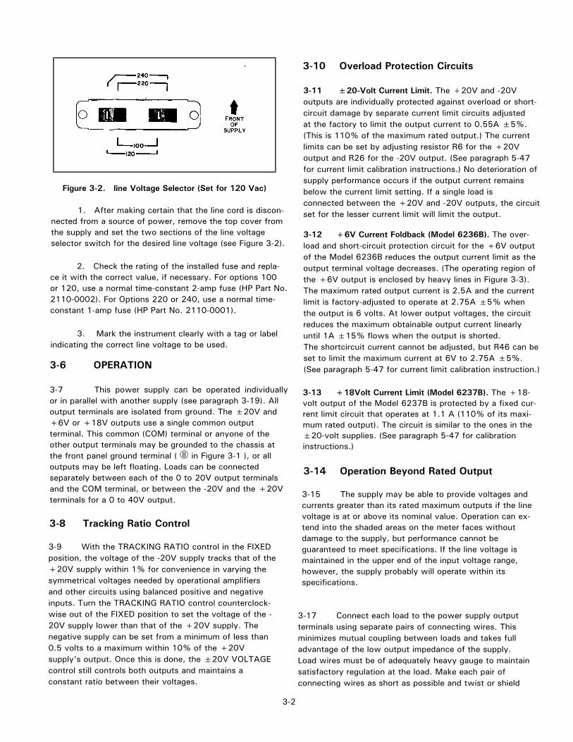
Figure 3-1. Controls and Indicators
3-2 The following steps describe the use of the Model6236B or 6237B front panel controls and indicators illus-trated in Figure 3-1 and serve as a brief check that the sup-ply is operational. Follow this checkout procedure or themore detailed performance test of paragraph 5-6 when theinstrument is received and before it is connected to anyload equipment. Proceed to the more detailed proceduresbeginning in paragraph 5-6 if any difficulties areencountered.
Before applying power to the supply, make certainthat its line voltage selector switch (S3) is set forthe line voltage to be used. This switch is mountedon the circuit board behind the voltmeter and isvisible through the perforations in the top cover.The positions of the two white marks on theswitch indicate the switch setting (see Figure 3-2).If the switch setting does not correspond to theintended power source, proceed to paragraph 3-4before applying power.
NOTE
For the Model 6237B, substitute+18Vfor +6V in the following steps.
a. Connect line cord to power source and turn LINEswitch on. LINE ON indicator will light.
b. Set METER switch to the +6V position and, withno load connected, vary +6V VOLTAGE control overits range and check that the voltmeter responds to thecontrol setting and the ammeter indicates zero.
c. Set the +6V VOLTAGE control for a 6-volt meterindication and short the +6V output terminal to COM(common) terminal with an insulated test lead. Theammeter should indicate a short-circuit output current ofapproximately 1.0A (1.1 A in the 6237B). Remove theshort from the output terminals.
d. Set the METER switch to the +20V position andturn TRACKING RATIO control fully clockwise to theFIXED position. With no load connected, vary ±20V VOL-TAGE control over its range and check that the volt-meter responds to the control setting and the ammeterindicates zero.
e. Set the ±20V VOLTAGE control for a 20-volt meterindication and short the +20V output terminal to the com-mon terminal with an insulated test lead. The ammetershould indicate a short-circuit output current of 0.55A±5%. Remove the short from the output terminals.
f. Repeat steps (d) and (e), but substitute the -20Vposition of the METER switch and the -20V output ter-minal.
g. Adjust the +20V output for a 20V meter indication.Then set the METER switch to the -20V position andcheck the effect of the TRACKING RATIO control on thevoltage of the -20V output. The -20V output should beadjustable from less than 0.5 volts to a maximum of 18 to22 volts.
3-3 If this brief checkout procedure or later use of thesupply reveals a possible malfunction, see Section V of thismanual for detailed test, troubleshooting, and adjustmentprocedures.
3-5 To convert the supply from one line voltage optionto another, the following three steps are necessary:
3-1
3-1 TURN-ON CHECKOUT PROCEDURE
———CAUTION———
3-4 LINE VOLTAGE OPTION CONVERSION
1. After making certain that the line cord is discon-nected from a source of power, remove the top cover fromthe supply and set the two sections of the line voltageselector switch for the desired line voltage (see Figure 3-2).
2. Check the rating of the installed fuse and repla-ce it with the correct value, if necessary. For options 100or 120, use a normal time-constant 2-amp fuse (HP Part No.2110-0002). For Options 220 or 240, use a normal time-constant 1-amp fuse (HP Part No. 2110-0001).
3. Mark the instrument clearly with a tag or labelindicating the correct line voltage to be used.
3-7 This power supply can be operated individuallyor in parallel with another supply (see paragraph 3-19). Alloutput terminals are isolated from ground. The ±20V and+6V or +18V outputs use a single common outputterminal. This common (COM) terminal or anyone of theother output terminals may be grounded to the chassis atthe front panel ground terminal ( in Figure 3-1 ), or alloutputs may be left floating. Loads can be connectedseparately between each of the 0 to 20V output terminalsand the COM terminal, or between the -20V and the +20Vterminals for a 0 to 40V output.
3-9 With the TRACKING RATIO control in the FIXEDposition, the voltage of the -20V supply tracks that of the+20V supply within 1% for convenience in varying thesymmetrical voltages needed by operational amplifiersand other circuits using balanced positive and negativeinputs. Turn the TRACKING RATIO control counterclock-wise out of the FIXED position to set the voltage of the -20V supply lower than that of the +20V supply. Thenegative supply can be set from a minimum of less than0.5 volts to a maximum within 10% of the +20Vsupply's output. Once this is done, the ±20V VOLTAGEcontrol still controls both outputs and maintains aconstant ratio between their voltages.
3-11 ±20-Volt Current Limit. The +20V and -20Voutputs are individually protected against overload or short-circuit damage by separate current limit circuits adjustedat the factory to limit the output current to 0.55A ±5%.(This is 110% of the maximum rated output.) The currentlimits can be set by adjusting resistor R6 for the +20Voutput and R26 for the -20V output. (See paragraph 5-47for current limit calibration instructions.) No deterioration ofsupply performance occurs if the output current remainsbelow the current limit setting. If a single load isconnected between the +20V and -20V outputs, the circuitset for the lesser current limit will limit the output.
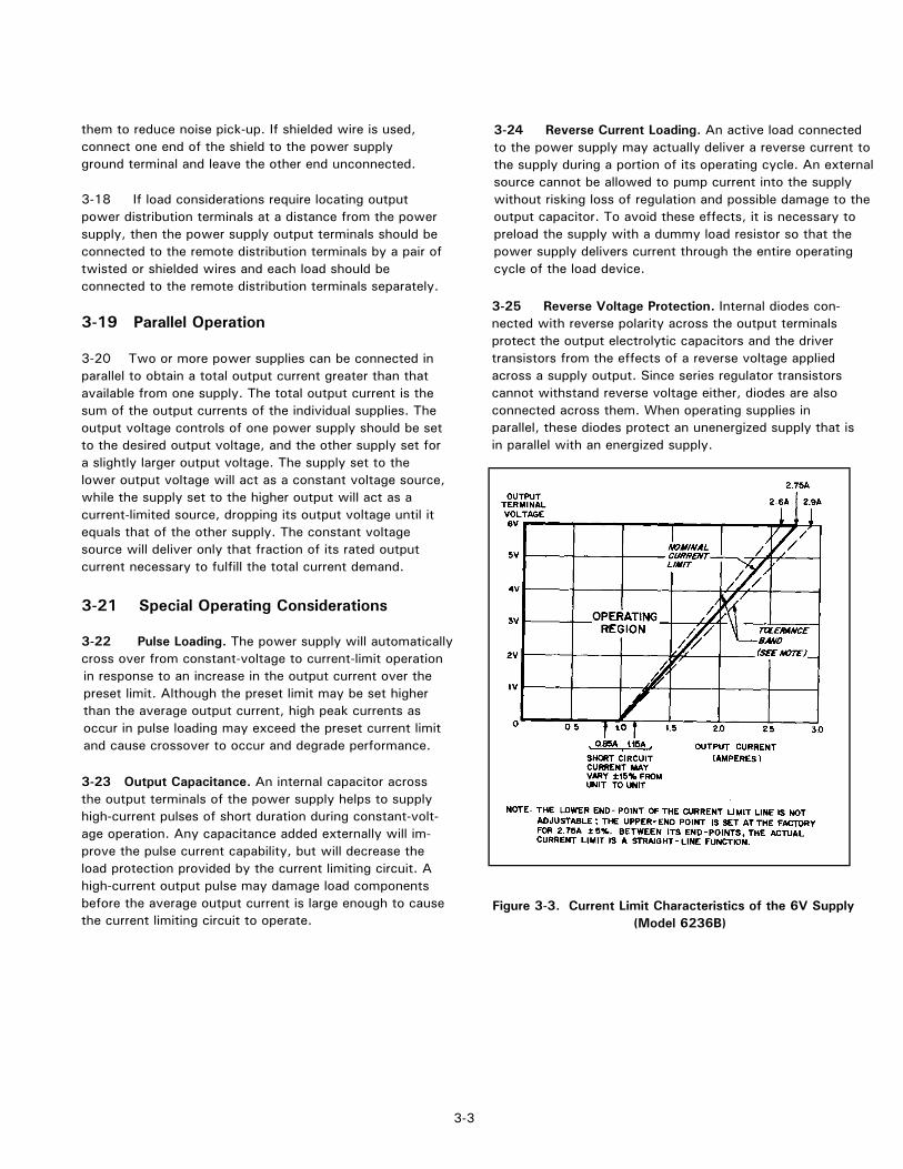
3-12 +6V Current Foldback (Model 6236B). The over-load and short-circuit protection circuit for the +6V outputof the Model 6236B reduces the output current limit as theoutput terminal voltage decreases. (The operating region ofthe +6V output is enclosed by heavy lines in Figure 3-3).The maximum rated output current is 2.5A and the currentlimit is factory-adjusted to operate at 2.75A ±5% whenthe output is 6 volts. At lower output voltages, the circuitreduces the maximum obtainable output current linearlyuntil 1A ±15% flows when the output is shorted.The shortcircuit current cannot be adjusted, but R46 can beset to limit the maximum current at 6V to 2.75A ±5%.(See paragraph 5-47 for current limit calibration instruction.)
3-13 +18Volt Current Limit (Model 6237B). The +18-volt output of the Model 6237B is protected by a fixed cur-rent limit circuit that operates at 1.1 A (110% of its maxi-mum rated output). The circuit is similar to the ones in the±20-volt supplies. (See paragraph 5-47 for calibrationinstructions.)
3-15 The supply may be able to provide voltages andcurrents greater than its rated maximum outputs if the linevoltage is at or above its nominal value. Operation can ex-tend into the shaded areas on the meter faces withoutdamage to the supply, but performance cannot beguaranteed to meet specifications. If the line voltage ismaintained in the upper end of the input voltage range,however, the supply probably will operate within itsspecifications.
3-17 Connect each load to the power supply outputterminals using separate pairs of connecting wires. Thisminimizes mutual coupling between loads and takes fulladvantage of the low output impedance of the supply.Load wires must be of adequately heavy gauge to maintainsatisfactory regulation at the load. Make each pair ofconnecting wires as short as possible and twist or shield
Figure 3-2. line Voltage Selector (Set for 120 Vac)
3-6 OPERATION
3-2
3-8 Tracking Ratio Control
3-14 Operation Beyond Rated Output
3-10 Overload Protection Circuits
them to reduce noise pick-up. If shielded wire is used,connect one end of the shield to the power supplyground terminal and leave the other end unconnected.
3-18 If load considerations require locating outputpower distribution terminals at a distance from the powersupply, then the power supply output terminals should beconnected to the remote distribution terminals by a pair oftwisted or shielded wires and each load should beconnected to the remote distribution terminals separately.
3-20 Two or more power supplies can be connected inparallel to obtain a total output current greater than thatavailable from one supply. The total output current is thesum of the output currents of the individual supplies. Theoutput voltage controls of one power supply should be setto the desired output voltage, and the other supply set fora slightly larger output voltage. The supply set to thelower output voltage will act as a constant voltage source,while the supply set to the higher output will act as acurrent-limited source, dropping its output voltage until itequals that of the other supply. The constant voltagesource will deliver only that fraction of its rated outputcurrent necessary to fulfill the total current demand.
3-22 Pulse Loading. The power supply will automaticallycross over from constant-voltage to current-limit operationin response to an increase in the output current over thepreset limit. Although the preset limit may be set higherthan the average output current, high peak currents asoccur in pulse loading may exceed the preset current limitand cause crossover to occur and degrade performance.
3-23 Output Capacitance. An internal capacitor acrossthe output terminals of the power supply helps to supplyhigh-current pulses of short duration during constant-volt-age operation. Any capacitance added externally will im-prove the pulse current capability, but will decrease theload protection provided by the current limiting circuit. Ahigh-current output pulse may damage load componentsbefore the average output current is large enough to causethe current limiting circuit to operate.
3-24 Reverse Current Loading. An active load connectedto the power supply may actually deliver a reverse current tothe supply during a portion of its operating cycle. An externalsource cannot be allowed to pump current into the supplywithout risking loss of regulation and possible damage to theoutput capacitor. To avoid these effects, it is necessary topreload the supply with a dummy load resistor so that thepower supply delivers current through the entire operatingcycle of the load device.
3-25 Reverse Voltage Protection. Internal diodes con-nected with reverse polarity across the output terminalsprotect the output electrolytic capacitors and the drivertransistors from the effects of a reverse voltage appliedacross a supply output. Since series regulator transistorscannot withstand reverse voltage either, diodes are alsoconnected across them. When operating supplies inparallel, these diodes protect an unenergized supply that isin parallel with an energized supply.
Figure 3-3. Current Limit Characteristics of the 6V Supply(Model 6236B)
3-3
3-19 Parallel Operation
3-21 Special Operating Considerations
SECTION IVPRINCIPLES OF OPERATION
4-2 This section presents the principles of operationof the Models 6236B and 6237B Triple Output PowerSupply. Throughout this section refer to the combinedschematic diagram of Figure 7-1.
NOTE
All information in this section applies to bothmodels unless otherwise indicated.
4-3 The two primary windings of the power transformerare connected in one of four different ways by setting thetwo slide switches mounted on the circuit board. Theseswitches select one of the nominal ac input voltages forwhich the supply is designed: 100V, 120V, 220V, or 240V.
4-4 The transformer secondaries, together withrectifiers and capacitor filters, provide raw dc for the threeoutput regulator circuits and for another regulator that pro-vides reference and bias voltages to the output regulators.
4-5 By comparing its output to a high-stability refer-ence, the 0 to +6-volt regulator (6236B) or 0 to +18-volt regulator (6237B) holds its output voltage at thevalue determined by a front panel control. Any error inthe actual output as compared to the desired output isamplified by an operational amplifier and applied asfeedback to control the conduction of a series regulatortransistor. As a result, the voltage across the seriestransistor varies so as to hold the output voltage constantat the desired level. The high gain of the voltagecomparison amplifier and the stability of the referencevoltage ensure that input voltage or load currentvariations have little effect on the output voltage.
4-6 The 0 to +6-volt output in the Model 6236B isprotected by a current foldback limiter to minimizedissipation in the series regulator transistor duringoverloads. In a current foldback circuit, the current limitdepends on the output terminal voltage and in this regulatorranges from 2.75A±5% at 6 volts to 1A±15% with theoutput shorted. (An output of 2.75A is 110% of the 2.5Arated maximum at 6 volts.) The operating region of the+6-volt regulator output is enclosed by a heavy line inFigure 3-3. If the operating point reaches the diagonalcurrent limit line, a decrease in load resistance moves theoperating point down the line, reducing the output voltage
and current. Current foldback is controlled by a secondoperational amplifier in the regulator that monitors the dcoutput current. This current comparison amplifier takescontrol of the output away from the voltage comparisonamplifier when the current reaches the design limit.Removing the overload restores constant voltageoperation automatically.
4-7 The +20-volt regulator has a fixed current limit at110% of its 0.5 amp maximum rated output but isotherwise similar to the +6-volt regulator.
4-8 The 0 to -20-volt regulator is, in turn, similar to the+20-volt regulator except that it resembles acomplementary mirror image of the latter. The outputvoltages of the +20volt and -20-volt supplies are both setby the same front panel control and track each other within1% in the fixed tracking ratio mode. Precise tracking of thetwo outputs is achieved by controlling the positive outputconventionally and using that output as the referencevoltage for the negative output.
4-9 The 0 to +18-volt regulator in the Model 6237Bis similar to the +20-volt regulator. It has a fixed currentlimit at 110% of its 1.0 amp output.
4-10 The reference and bias supply provides referenceand bias voltages for the output regulators.
4-11 The turn-on/turn-off control circuit prevents outputtransients when the supply is turned on or off. It does this bydelaying the application of certain bias and reference voltagesat turn-on and removing them shortly after turn-off.
4-12 A three-position meter switch selects which ofthe supplies has its output voltage and current indicatedon the front panel meters. The proper range of the dual-range meters is selected automatically
4-15 Voltage Comparison Amplifier. The voltage com-parison amplifier in the +20-volt supply controls the conduc-tion of series regulator transistor Q1 so that the voltages atthe two inputs of the amplifier remain equal. A fixed voltagedivider holds its inverting input (U1-2) at -16mV. Its non-inverting input (U1-3) monitors the output voltage in series
4-1
4-1 OVERALL DESCRIPTION
4-13 DETAILED CIRCUIT DESCRIPTION
4-14 0 To +20-Volt Regulator
with the voltage across R1. Since R2 is connected betweenthe -6.2V reference supply and a point that feedback actionholds near -16mV, its current remains constant. Thiscurrent flows through R1 to produce a voltage drop acrossR1 proportional to its resistance setting, thus the outputvoltage of the supply is proportional to the resistancesetting of R1. At the output of the voltage comparisonamplifier (U1-1), a positive voltage change corresponds to adecrease in the conduction of Q1.
4-16 CR2 and CR3 protect the input of the amplifieragainst transient overloads, C2 and R4 speed up loopresponse time, and C4 and R12 stabilize the supply'shigh frequency characteristics.
4-17 OR-Gate. To permit either the voltage comparisonamplifier or the current comparison amplifier to control theseries regulator transistor, the outputs of both amplifiersare connected to the base of driver Q2 through an OR-gatecomposed of CR5 and CR6. CR5 is normally reversebiased by a negative output from the current comparisonamplifier, permitting the voltage comparison amplifier todrive Q2 through CR6. An overload drives the output ofthe current comparison amplifier positive, forward biasingCR5 and reducing the supply output. When the overload isremoved, CR5 is reverse biased again and the voltage com-parison amplifier resumes control of the output.
4-18 Driver and Series Regulator. The -12.4V output ofthe bias supply provides the turn-on bias for seriesregulator transistor Q1. Its complete current path includesQ15, CR59, R 14, and Q1, and returns to commonthrough current monitoring resistor R8. (It is because thisbias current flows through R8 that the output ammeterrequires the zero offset bias circuit described in paragraph4-43.) Through the OR-gate, either the voltage or thecurrent comparison amplifier controls the conduction ofdriver Q2, which regulates the flow of turn-off biasthrough Q1's base-emitter circuit. The algebraic sum of thenearly constant turn-on bias through R14 and the variableturn-off bias through Q2 controls the conduction of seriesregulator transistor Q1.
4-19 Current Limit Circuit. In the +20-volt regulator,the current comparison amplifier compares the voltageacross current monitoring resistor R8 to the fixed voltageacross part of current limit adjust potentiometer R6. Thecurrent limit adjustment is set so that the input voltage tothe current comparison amplifier is negative in the normaloperating region, but becomes zero when the outputcurrent increases to 0.55 amps. When the amplifier'sinput voltage reaches zero, it takes control of theregulator output voltage and reduces it as necessary tokeep the output current from exceeding 0.55 amps.When the overload is removed, the output of the currentcomparison amplifier goes negative, reverse biasing CR5
and returning control to the voltage comparison amplifier.
4-20 Turn-On/Turn-Off Control. When the power supplyis turned on or off, Q15 in the turn-on control circuit with-holds turn-on bias from Q1 while the regulator bias voltagesare too low. This prevents an output voltage transient fromoccurring before the amplifiers are properly biased. Theoutput of the -6.2V reference supply is also temporarilyheld at a low voltage by Q14, which conducts to short thatoutput.
4-21 Circuit Protection Components. Diodes CR1, CR7,and CR9 each protect the +20-volt supply from specifichazards. Output diode CR1 protects the supply componentsif a reverse voltage is applied to the output terminals. Acommon way for this to occur is for an unenergized supplyto be connected in series with another that is energized. Ifthe output voltage is turned down quickly while a largecapacitor is connected across the output, CR7 protectsdriver Q2 from excessive dissipation by shunting some of itsbase current to common. The series regulator diode, CR9,protects the series regulator transistor from reverse voltage.Reverse series regulator voltage could occur if a deenergizedsupply were connected in parallel with an energized one.
4-23 Instead of using an NPN driver and a PNP seriesregulator in the negative output line as in the +20-voltregulator, the -20-volt regulator uses a PNP driver and anNPN series regulator in the positive output line. The -20-volt regulator circuit is the complementary equivalent ofthe +20-volt circuit in other respects, as well. Theircurrent limit circuits operate similarly. At the outputs ofthe current and voltage comparison amplifiers in the -20-volt circuit, a negative voltage change corresponds to adecrease in series regulator conduction. The turn-on biasfor its series regulator transistor, Q3, is supplied from apositive voltage source, the +7.5V bias supply, and isswitched on and off by Q13 in the turn-on control circuit.
4-24 The -20-volt supply uses the output of the +20-volt supply as its reference voltage. As a result, bothoutputs are set by a single front panel control and trackeach other with in 1% in the fixed tracking ratio mode.Two resistors in resistor network Z1 are connected inseries between the +20volt and -20-volt outputs. Theseresistors are closely matched in resistance and temperaturecoefficient so that the voltage across each is exactly halfof the total. The midpoint of this divider is connected tothe non-inverting input of the -20-volt supply's voltagecomparison amplifier. The amplifier's inverting input isconnected to common through R32 to hold it at zero volts.The amplifier keeps its differential input voltage at zero bymatching the output voltage of the -20-volt supply to thatof the +20-volt supply.
4-2
4-22 0 To -20-Volt Regulator
4-25 In the variable tracking ratio mode, the trackingratio control connects a fixed resistor in parallel withthe upper part and a rheostat (the variable tracking ratiocontrol) in parallel with the lower part of the voltagedivider that forms the -20-volt reference. Turning thecontrol counter- clockwise reduces the resistance of therheostat and lowers the voltage of the negative output.
4-27 Except for differing component designations andvalues, paragraphs 4-15 through 4-18,4-20, and 4-21,which describe the voltage comparison amplifier, OR-gate,driver, series regulator, turn-on control, and circuitprotection components of the +20-volt regulator circuit,also apply to the +6-volt regulator. The only difference incircuit operation lies in the control of the currentcomparison amplifier, and thus the type of current limit thesupply has.
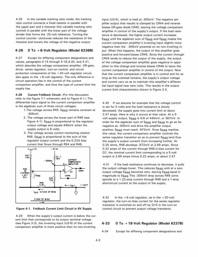
4-28 Current Foldback Circuit. (For this discussionrefer to the Figure 7-1 schematic and to Figure 4-1.) Thedifferential input signal to the current comparison amplifieris the algebraic sum of three circuit voltages: 1.The voltage across R49. ER49 remains constant at
-305mV.2. The voltage across the lower part of R46 (see
Figure 4-1). ER49 is proportional to the regulatoroutput voltage and equals 440mV when thesupply output is 6 volts.
3. The voltage across current monitoring resistorR48. ER48 is proportional to the sum of theregulator output current and the 0.22A biascurrent that flows through R54 and R48.
Figure 4-1. Foldback Current Limit Circuit in 6V Supply
4-29 When the supply's output current is below the cur-rent limit that corresponds to its output terminal voltage(see Figure 3-3), the inverting input (U3-6) of the currentcomparison amplifier is more positive than its non-inverting
input (U3-5), which is held at -305mV. The negative am-plifier output that results is clamped by CR44 and reversebiases OR-gate diode CR45, leaving the voltage comparisonamplifier in control of the supply's output. If the load resis-tance is decreased, the higher output current increasesER48 until the algebraic sum of ER48 and ER46 makes thecurrent comparison amplifier's inverting input slightly morenegative than the -305mV potential on its non-inverting in-put. When this happens, the output of this amplifier goespositive and forward biases CR45. Since the current throughCR45 tends to reduce the output of the supply, the outputof the voltage comparison amplifier goes negative in oppo-sition to this change and reverse biases CR46 to leave thecurrent comparison amplifier in control of the output. Nowthat the current comparison amplifier is in control and for aslong as the overload remains, the supply's output voltageand current vary so as to maintain this amplifier's differen-tial input signal near zero volts. This results in the outputcurrent limit characteristics shown in Figure 3-3.
4-30 If we assume for example that the voltage controlis set for 5 volts and the load resistance is slowlydecreased, the supply goes into current limit at about2.47 amps. Here is why it occurs at that value. At a 5-volt supply output, ER46 is 5/6 of 440mV, or 367mV. Inorder for the algebraic sum of ER46 and ER48 to go as farnegative as -305mV and drive the amplifier outputpositive, ER48 must reach -672mV. Once ER48 reachesthis value, the current comparison amplifier controls theseries regulator transistor so as to prevent ER48 (and thusthe supply's output current) from increasing further. At0.25 ohms, R48 develops -672mV at 2.69 amps. Since0.22 amps of the current through R48 is bias current forQ7, the nominal current limit corresponding to a 5-voltoutput is 2.69 amps minus 0.22 amps, or about 2.47
4-31 If the load resistance continues to decrease, it pullsthe output voltage lower. This reduces ER46 until at a zerooutput voltage ER46 becomes zero, leaving ER48 equal inmagnitude to ER49 This -305mV drop across R48 corre-sponds to a 1.22-amp current through R48 and a 1-ampshortcircuit current at the output of the supply.
4-32 In the +6-volt regulator, as in the +20-voltregulator, the turn-on bias current for the series regulatortransistor is switched on and off by Q15 in the turn-oncontrol circuit to prevent output voltage transients.
4-3
4-33 0 To +18-Volt Regulator (Model 6237B)
4-34 Except for differing component designations and
4-26 0 To +6-Volt Regulator (Model 6236B)
values, paragraphs 4-15 through 4-21, which describe thevoltage comparison amplifier, OR-gate, driver, series regu-lator, current limit circuit, turn-on control, and circuitprotection components of the +20-volt regulator circuit,also apply to the +18-volt regulator. In the +18-voltregulator, as in the +20-volt regulator, the turn-on biascurrent for the series regulator transistor is switched on andoff by Q15 in the turn-on control circuit to prevent outputvoltage transients.
4-35 Reference and Bias Supply
4-36 The reference and bias supply powers theoperational amplifiers and provides the bias and referencevoltages used throughout the supply. A shunt zenerregulates its +7.5V output. A series transistor regulates its-12.4 V output, using 6.2-volt zener VR1 as its voltagereference. The -12.4V output provides a constant current toVR1, which is the primary voltage reference for the entiresupply.4-37 Two equal resistors are connected in seriesacross the -12.4V output. To regulate this output,voltage comparison amplifier U4 compares the voltageacross one of these resistors to the -6.2V reference andcontrols the conduction of series regulator Q11 throughdriver Q12. The voltage drop across Q11 is controlledby feedback so that the voltages at the two inputs of U4remain equal. Driver Q12 controls Q11 by shunting partof the base bias supplied by R68.
4-38 During turn-on, the -6.2V reference supply istemporarily shorted by Q14 in the turn-on control circuit.By trying to match this low reference, Q11 is initially turnedoff. While Q11 is turned off, R69 bypasses current to the-12.4 V output until the output reaches -9 volts and theturn-on control circuit removes the short from the referenceand enables the -12.4-volt regulator to operate normally.
4-39 Turn-On/Turn-Off Control Circuit
4-40 Immediately after the supply is energized anduntil the output of the -12.4-volt regulator reaches about-9 volts, the turn-on control circuit withholds turn-on biasfrom series regulator transistors Q1, Q3, and Q7 and holdsthe -6.2V reference at a low value. This prevents an outputvoltage transient by ensuring that the operational amplifiersare energized and other essential bias voltages are presentbefore the series regulator transistors are turned on. Thecircuit also prevents an output transient when the supply isturned off by removing the turn-on bias from the seriesregulators and shorting the -6.2V reference supply as thevoltage of the -12.4 V supply falls below -9 volts.
4-41 Q13 switches the bias to the -20-volt regulatoron and off, Q14 switches the short across the -6.2-voltreference supply, and Q15 switches the bias to the +20-volt and +6-volt or +18-volt regulators. Q15 remainsturned off until VR2 conducts at 9 volts to switch it on.While Q15 is off, it holds Q13 biased off and Q14 on;when Q15 conducts, it turns Q13 and Q14 off.
4-42 Meter Circuits
4-43 Voltmeter. Two of the resistors in resistornetwork Z1 are range resistors for the voltmeter. Theaccurate ratio of these resistors permits a single calibrationpotentiometer, R58 to adjust both ranges simultaneously.
4-44 Ammeter. The range switch connects theammeter across the current monitoring resistor of a supply:R48 in the +6-volt or +18-volt supply, R8 in the +20-voltsupply, or R28 in the -20-volt supply. Each of theseresistors conducts a constant bias current for its seriesregulator transistor in addition to the supply's outputcurrent. If no compensation were used, this additionalcurrent would raise the indicated output by up to 8% of fullscale. The resistor networks connected to each range of theammeter selector switch apply a bias to the meter to offsetthis error. R59 calibrates all ammeter ranges.
4-4
SECTION VMAINTENANCE
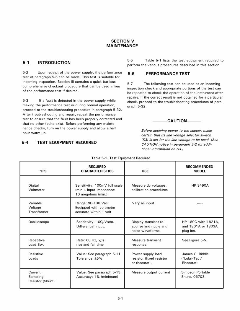
5-1 INTRODUCTION 5-5 Table 5-1 lists the test equipment required toperform the various procedures described in this section.
5-6 PERFORMANCE TEST5-2 Upon receipt of the power supply, the performancetest of paragraph 5-6 can be made. This test is suitable forincoming inspection. Section III contains a quick but lesscomprehensive checkout procedure that can be used in lieuof the performance test if desired.
5-3 If a fault is detected in the power supply whilemaking the performance test or during normal operation,proceed to the troubleshooting procedure in paragraph 5-32.After troubleshooting and repair, repeat the performancetest to ensure that the fault has been properly corrected andthat no other faults exist. Before performing any mainte-nance checks, turn on the power supply and allow a halfhour warm-up.
5-4 TEST EQUIPMENT REQUIRED
5-7 The following test can be used as an incominginspection check and appropriate portions of the test canbe repeated to check the operation of the instrument afterrepairs. If the correct result is not obtained for a particularcheck, proceed to the troubleshooting procedures of para-graph 5-32.
———CAUTION———
Before applying power to the supply, makecertain that its line voltage selector switch(S3) is set for the line voltage to be used. (SeeCAUTION notice in paragraph 3-2 for addi-tional information on S3.)
Table 5-1. Test Equipment Required
5-1
REQUIRED RECOMMENDED TYPE CHARACTERISTICS USE MODEL
Digital Sensitivity: 100mV full scale Measure dc voltages: HP 3490AVoltmeter (min.). Input impedance: calibration procedures 10 megohms (min.).
Variable Range: 90-130 Vac Vary ac input -----Voltage Equipped with voltmeterTransformer accurate within 1 volt
Oscilloscope Sensitivity: 100µV/cm. Display transient re- HP 180C with 1821A, Differential input. sponse and ripple and and 1801A or 1803A
noise waveforms. plug-ins.
Repetitive Rate: 60 Hz, 2µs Measure transient See Figure 5-5.Load Sw. rise and fall time response.
Resistive Value: See paragraph 5-11. Power supply load James G. BiddleLoads Tolerance: ±5% resistor (fixed resistor ("Lubri-Tact"
or rheostat). Rheostat)
Current Value: See paragraph 5-13. Measure output current Simpson PortableSampling Accuracy: 1% (minimum) Shunt, 06703.Resistor (Shunt)
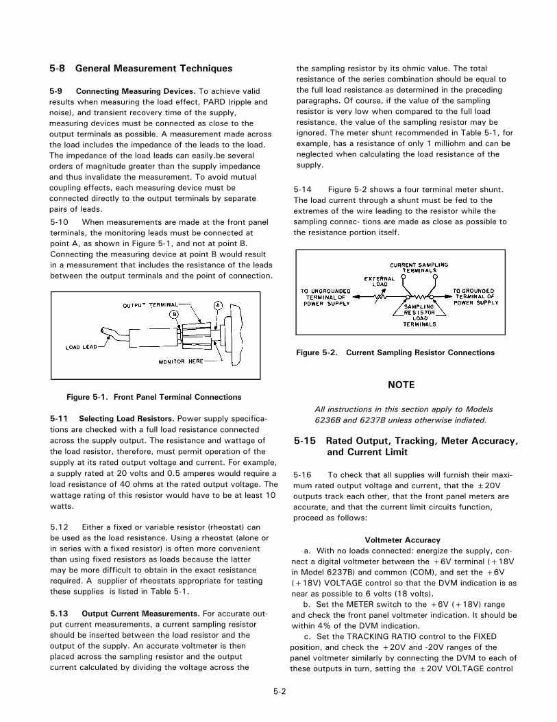
5-9 Connecting Measuring Devices. To achieve validresults when measuring the load effect, PARD (ripple andnoise), and transient recovery time of the supply,measuring devices must be connected as close to theoutput terminals as possible. A measurement made acrossthe load includes the impedance of the leads to the load.The impedance of the load leads can easily.be severalorders of magnitude greater than the supply impedanceand thus invalidate the measurement. To avoid mutualcoupling effects, each measuring device must beconnected directly to the output terminals by separatepairs of leads.
5-10 When measurements are made at the front panelterminals, the monitoring leads must be connected atpoint A, as shown in Figure 5-1, and not at point B.Connecting the measuring device at point B would resultin a measurement that includes the resistance of the leadsbetween the output terminals and the point of connection.
Figure 5-1. Front Panel Terminal Connections
5-11 Selecting Load Resistors. Power supply specifica-tions are checked with a full load resistance connectedacross the supply output. The resistance and wattage ofthe load resistor, therefore, must permit operation of thesupply at its rated output voltage and current. For example,a supply rated at 20 volts and 0.5 amperes would require aload resistance of 40 ohms at the rated output voltage. Thewattage rating of this resistor would have to be at least 10watts.
5.12 Either a fixed or variable resistor (rheostat) canbe used as the load resistance. Using a rheostat (alone orin series with a fixed resistor) is often more convenientthan using fixed resistors as loads because the lattermay be more difficult to obtain in the exact resistancerequired. A supplier of rheostats appropriate for testingthese supplies is listed in Table 5-1.
5.13 Output Current Measurements. For accurate out-put current measurements, a current sampling resistorshould be inserted between the load resistor and theoutput of the supply. An accurate voltmeter is thenplaced across the sampling resistor and the outputcurrent calculated by dividing the voltage across the
the sampling resistor by its ohmic value. The totalresistance of the series combination should be equal tothe full load resistance as determined in the precedingparagraphs. Of course, if the value of the samplingresistor is very low when compared to the full loadresistance, the value of the sampling resistor may beignored. The meter shunt recommended in Table 5-1, forexample, has a resistance of only 1 milliohm and can beneglected when calculating the load resistance of thesupply.
5-14 Figure 5-2 shows a four terminal meter shunt.The load current through a shunt must be fed to theextremes of the wire leading to the resistor while thesampling connec- tions are made as close as possible tothe resistance portion itself.
Figure 5-2. Current Sampling Resistor Connections
NOTE
All instructions in this section apply to Models6236B and 6237B unless otherwise indiated.
5-16 To check that all supplies will furnish their maxi-mum rated output voltage and current, that the ±20Voutputs track each other, that the front panel meters areaccurate, and that the current limit circuits function,proceed as follows:
Voltmeter Accuracya. With no loads connected: energize the supply, con-
nect a digital voltmeter between the +6V terminal (+18Vin Model 6237B) and common (COM), and set the +6V(+18V) VOLTAGE control so that the DVM indication is asnear as possible to 6 volts (18 volts).
b. Set the METER switch to the +6V (+18V) rangeand check the front panel voltmeter indication. It should bewithin 4% of the DVM indication.
c. Set the TRACKING RATIO control to the FIXEDposition, and check the +20V and -20V ranges of thepanel voltmeter similarly by connecting the DVM to each ofthese outputs in turn, setting the ±20V VOLTAGE control
5-2
5-15 Rated Output, Tracking, Meter Accuracy, and Current Limit
5-8 General Measurement Techniques
for a 20V DVM indication, and verifying that the panelmeter is accurate within 4%.
Trackingd. Connect the DVM to the +20V output, set the ±20V
VOLTAGE control for a DVM indication of 20 volts, andreconnect the DVM to the -20V output without disturbingthe voltage control. The voltage at the -20V output shouldbe within 1% of the +20Voutput.
Variable Tracking Ratioe. Leave the ±20V VOLTAGE control set as in step (d),
and use a DVM to monitor the voltage of the -20V supplywhile adjusting the TRACKING RATIO control over itsVARIABLE range. The -20V supply should be capable ofbeing adjusted from less than 0.5 volts to between 18and 22 volts. Return the TRACKING RATIO control to theFIXED position.
NOTE
Leave the TRACKING RATIO control in theFIXED position throughout the remainder of theperformance test.
Rated Output and Ammeter Accuracyf. Connect 40Ω 10W load resistors across both of the 20V
outputs of the supply and set the ±20V VOLTAGE control for a±20V output. (All three supplies must be fully loaded whilechecking the rated output voltage and current of each supply.)
g. Connect the test setup shown in Figure 5-3 to the +6V(or +18V) output. Make the total resistance of RL and thecurrent sampling resistor 2.4 ohms for the Model 6236B (or18 ohms for the 6237B) to permit operating the output at fullload. RL should have a power rating of at least 20 watts.
h. Close the switch and set the +6V (+18V) VOLTAGEcontrol so that the DVM indicates a voltage drop across thecurrent sampling resistor that corresponds to a current of 2.5amps (6236B) or 1.0 amp (6237B).
i. Set the METE R switch to the +6V (+18V) range andverify that the front panel ammeter indication is within 4% of2.5 amps (6236B) or 1.0 amp (6237B).
j. Connect the DVM directly across the output terminals ofthe +6V (+18V) supply, record the DVM reading, and thenopen the switch in the 6V (18V) load circuit without disturbingthe supply's output terminals. The DVM indication should notchange by more than 2.6mV (6236B) or 3.8mV (6237B).
k. Check the rated output and ammeter accuracy of the+20V and -20V supplies similarly by connecting the test setupof Figure 5-3 to each output in turn. For each 20V supply:make the total resistance of RL and the current samplingresistor 40 ohms, set the ±20V VOLTAGE control for a currentindication, on the DVM of 0.5A, check that panel meter
indication is within 4% of 0.5A, connect the DVM tothe fully loaded output terminals, and compare theoutput voltage before and after the load circuit isopened. The voltage should not change by more than4mV. While checking each supply, the other two mustbe fully loaded.
Current Limitl. Disconnect all loads from the supply.m. Connect the test setup shown in Figure 5-3 to the
+20 volt output. Substitute a short for RL and leave theload circuit switch open. n. Set the voltage of the ±20V supplies to 20-volts. o. Close the load switch and determine the currentflow through the current sampling resistor (meter shunt)by measuring its voltage drop with the DVM. The currentshould be 0.55A ±5%.
p. Check the current limit of the -20V supply in thesame way. Its short-circuit current should also be 0.55A±5%.
q. (Model 6237B only). Check the current limit of the+18V supply similarly by setting its output for 18 voltsand using a DVM to measure the current which flowsthrough a low- resistance current sampling resistor. Theshort-circuit current of the +18V supply should be 1.1 A±5%.
r. (Steps (r) through (t) apply to the 6236B only.)Connect the test setup shown in Figure 5-3 to the +6Voutput. Close the switch, set the total resistance of RL andthe current sampling resistor to an initial value of 2.4 ohmsor greater, and set the output voltage to 6 volts.
s. Reduce the value of RL gradually while observing theoutput current indicated by the DVM. The current shouldincrease to a maximum of 2.75A ±5% before it begins todecrease.
t. Connect a short across RL and then recheck thecurrent
5-17 Load Effect (Load Regulation) Definition: The change ∆EOUT in the static value of dcoutput voltage resulting from a change in loadresistance from open circuit to the value that yieldsmaximum rated output current (or vice versa).
5-18 To check the load effect:a. Connect a full load resistance and a digital voltmeter
across the output of the +20V supply. b. Turn on the supply and adjust its voltage to itsmaximum rated value.
c. Record the voltage indicated on the DVM.d. Disconnect the load resistance and recheck the DVM
indication. It should be within .01% plus 2mV of the read-ing in step (c).
e. Repeat steps (a) through (d) for each of the remain-ing supply outputs.
5-3
5-20 To test the source effect:a. Connect a variable autotransformer between the in
put power source and the power supply line plug.b. Connect a full load resistance and a digital voltmeter
across the output of the +20V supply. c. Adjust the autotransformer for a low line input.
d. Turn on the power, adjust the output of the supplyto its maximum rated voltage, and record the DVM indica-tion.
e. Adjust the autotransformer for a high line input andrecheck the DVM indication. It should be within .01% plus2mV of the reading in step (d).
f. Repeat steps (b) through (e) for each of theremaining supply outputs.
5-22 Measurement Techniques. Figure 5-4A shows anincorrect method of measuring p-p ripple. Note that a con-tinuous ground loop exists from the third wire of the inputpower cord of the supply to the third wire of the inputpower cord of the oscilloscope via the grounded powersupply case, the wire between the negative outputterminal of the power supply and the vertical input of thescope, and the grounded scope case. Any ground currentcirculating in this loop as a result of the difference inpotential EG between the two ground points causes an IRdrop that is in series with the scope input. This IR drop,normally having a 60 Hz line frequency fundamental, plusany pickup on the unshielded leads interconnecting thepower supply and scope, appears on the face of the CRT.
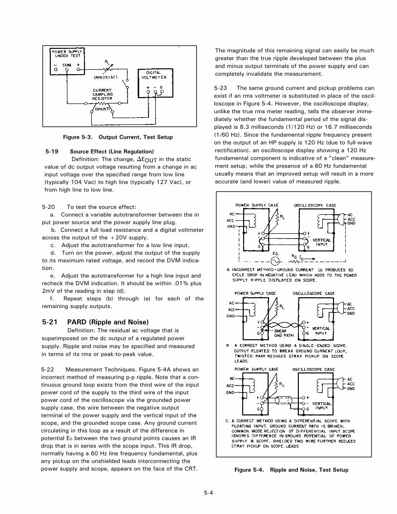
The magnitude of this remaining signal can easily be muchgreater than the true ripple developed between the plusand minus output terminals of the power supply and cancompletely invalidate the measurement.
5-23 The same ground current and pickup problems canexist if an rms voltmeter is substituted in place of the oscil-loscope in Figure 5-4. However, the oscilloscope display,unlike the true rms meter reading, tells the observer imme-diately whether the fundamental period of the signal dis-played is 8.3 milliseconds (1/120 Hz) or 16.7 milliseconds(1/60 Hz). Since the fundamental ripple frequency presenton the output of an HP supply is 120 Hz (due to full-waverectification). an oscilloscope display showing a 120 Hzfundamental component is indicative of a "clean" measure-ment setup, while the presence of a 60 Hz fundamentalusually means that an improved setup will result in a moreaccurate (and lower) value of measured ripple.
5-4
5-19 Source Effect (Line Regulation) Definition: The change, ∆EOUT in the staticvalue of dc output voltage resulting from a change in acinput voltage over the specified range from low line(typically 104 Vac) to high line (typically 127 Vac), orfrom high line to low line.
Figure 5-4. Ripple and Noise, Test Setup
5-21 PARD (Ripple and Noise) Definition: The residual ac voltage that issuperimposed on the dc output of a regulated powersupply. Ripple and noise may be specified and measuredin terms of its rms or peak-to-peak value.
Figure 5-3. Output Current, Test Setup
5-24 Figure 5-4B shows a correct method of measuringthe output ripple of a constant voltage power supplyusing a single-ended scope. The ground loop path isbroken by floating the power supply output. To ensurethat no potential difference exists between the supplyand the oscilloscope, it is recommended that they bothbe plugged into the same ac power bus. If the same buscannot be used, both ac grounds must be at earthground potential.5-25 Either a twisted pair or, preferably, a shielded two-wire cable should be used to connect the output terminalsof the power supply to the vertical input terminals of thescope. When using a twisted pair, care must be taken thatone of the two wires is connected to the grounded inputterminal of the oscilloscope to ensure that the supplyoutput is safely grounded. When using shielded two-wire, itis essential for the shield to be connected to ground at oneend only to prevent ground current flowing through thisshield from inducing a signal in the shielded leads.
5-26 To verify that the oscilloscope is not displayingripple that is induced in the leads or picked up from thegrounds, the (+) scope lead should be shorted to the (-)scope lead at the power supply terminals. The ripple valueobtained when the leads are shorted should be subtractedfrom the actual ripple measurement.
5-27 In most cases, the single-ended scope method ofFigure 5-4B will be adequate to eliminate extraneous rippleso that a satisfactory measurement may be obtained.However, in more stubborn cases (or if high frequencynoise up to 20 MHz must be measured). it may benecessary to use a differential scope with floating input asshown in Figure 5-4C. If desired, two single-conductorshielded cables may be substituted in place of the shieldedtwo-wire cable with equal success. Because of its commonmode rejection. a differential oscilloscope displays only thedifference in signal between its two vertical input terminals,thus ignoring the effects of any common mode signal pro-duced by the difference in the ac potential between thepower supply case and scope case. Before using a differen-tial input scope in this manner, however, it is imperativethat the common mode rejection capability of the scope beverified by shorting together its two input leads at thepower supply and observing the trace on the CRT. If thistrace is a straight line, then the scope is properly ignoringany common mode signal present. If this trace is not astraight line, then the scope is not rejecting the groundsignal and must be realigned in accordance with the manu-facturer's instructions until proper common mode rejectionis attained
5-28 Measurement Procedure. To measure the rippleand noise on each supply output, follow the stepsbelow, If a high frequency noise measurement is desired,
an oscilloscope with sufficient bandwidth (20 MHz) mustbe used. Ripple and noise measurements can be made atany input ac line voltage combined with any dc outputvoltage and load current within rating.
a. Connect an oscilloscope or rms voltmeter across anoutput of the supply as shown in Figures 5-4B or 5-4C.
b. Energize the supply and observe the oscilloscope ormeter indication. The ripple and noise should not begreater than 0.35mV rms or 1.5mV peak-to-peak. c. Repeat for the remaining supply outputs.
5-30 Measurement Techniques. Care must be taken inswitching the load resistance on and off. A hand-operatedswitch in series with the load is not adequate since the re-sulting one-shot displays are difficult to observe on mostoscilloscopes and the arc energy occurring during switchingcompletely masks the display with a noise burst. Transistorload switching devices are expensive if reasonably rapid load
Figure 5-5. Load Transient Recovery Time, Test Setup
5-5
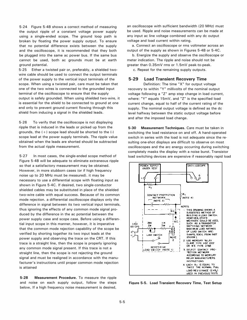
5-29 Load Transient Recovery TimeDefinition: The time "X" for output voltage
recovery to within "Y" millivolts of the nominal outputvoltage following a "Z" amp step change in load current,where: "Y" equals 15mV, and "Z" is the specified loadcurrent change, equal to half of the current rating of thesupply. The nominal output voltage is defined as the dclevel halfway between the static output voltage beforeand after the imposed load change.
current changes are to be achieved. Instead, a mercury-wetted relay should be used for loading and unloading thesupply. Connect it in the load switching circuit shown inFigure 5-5. When this load switch is connected to a 60 Hzac input, the mercury-wetted relay will open and close 60times per second. The 25K control adjusts the duty cycleof the load current switching to reduce jitter in the oscillo-scope display. This relay may also be used with a 50 Hz acinput.
5-31 Measurement Procedure. To measure the loadtransient recovery time, follow the steps below for eachsupply output. Transient recovery time may be measured atany input line voltage and any output voltage within rating.For this supply the specified load change is between half loadand full load.
a. Connect the test setup shown in Figure 5-5. Bothload resistors (RL) are twice the normal value of a full load
resistance.b. Turn on the supply and close the line switch on the
repetitive load switch.c. Set the oscilloscope for internal sync and lock on
either the positive or negative load transient spike.d. Set the vertical input of the oscilloscope for ac coup-
ling so that small dc level changes in the output voltage ofthe power supply will not cause the display to shift.
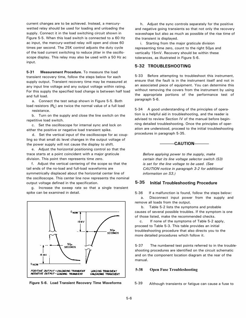
e. Adjust the horizontal positioning control so that thetrace starts at a point coincident with a major graticuledivision. This point then represents time zero.
f. Adjust the vertical centering of the scope so that thetail ends of the no-load and full-load waveforms aresymmetrically displaced about the horizontal center line ofthe oscilloscope. This center line now represents the nominaloutput voltage defined in the specification.
g. Increase the sweep rate so that a single transientspike can be examined in detail.
Figure 5-6. Load Transient Recovery Time Waveforms
h. Adjust the sync controls separately for the positiveand negative going transients so that not only the recoverywaveshape but also as much as possible of the rise time ofthe transient is displayed.
i. Starting from the major graticule divisionrepresenting time zero, count to the right 50µs andvertically 15mV. Recovery should be within thesetolerances, as illustrated in Figure 5-6.
5-32 TROUBLESHOOTING
5-33 Before attempting to troubleshoot this instrument,ensure that the fault is in the instrument itself and not inan associated piece of equipment. You can determine thiswithout removing the covers from the instrument by usingthe appropriate portions of the performance test ofparagraph 5-6.
5-34 A good understanding of the principles of opera-tion is a helpful aid in troubleshooting, and the reader isadvised to review Section IV of the manual before begin-ning detailed troubleshooting. Once the principles of oper-ation are understood, proceed to the initial troubleshootingprocedures in paragraph 5-35.
———CAUTION———
Before applying power to the supply, makecertain that its line voltage selector switch (S3)is set for the line voltage to be used. (SeeCAUTION notice in paragraph 3-2 for additionalinformation on S3.)
5-35 Initial Troubleshooting Procedure
5-36 If a malfunction is found, follow the steps below: a. Disconnect input power from the supply andremove all loads from the output. b. Table 5-2 lists the symptoms and probablecauses of several possible troubles. If the symptom is oneof those listed, make the recommended checks.
c. If none of the symptoms of Table 5-2 apply,proceed to Table 5-3. This table provides an initialtroubleshooting procedure that also directs you to themore detailed procedures which follow it.
5-37 The numbered test points referred to in the trouble-shooting procedures are identified on the circuit schematicand on the component location diagram at the rear of themanual.
5-38 Open Fuse Troubleshooting
5-39 Although transients or fatigue can cause a fuse to
5-6
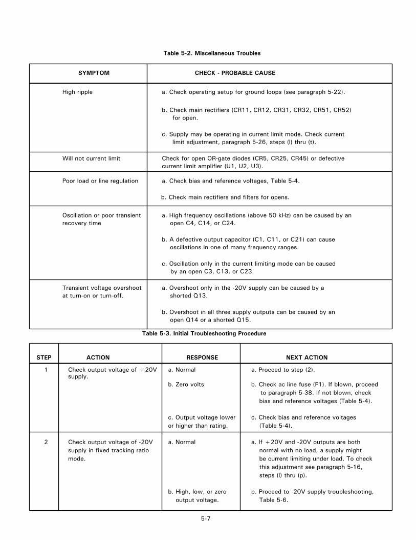
Table 5-2. Miscellaneous Troubles
SYMPTOM CHECK - PROBABLE CAUSE
High ripple a. Check operating setup for ground loops (see paragraph 5-22).
b. Check main rectifiers (CR11, CR12, CR31, CR32, CR51, CR52)for open.
c. Supply may be operating in current limit mode. Check currentlimit adjustment, paragraph 5-26, steps (l) thru (t).
Will not current limit Check for open OR-gate diodes (CR5, CR25, CR45) or defectivecurrent limit amplifier (U1, U2, U3).
Poor load or line regulation a. Check bias and reference voltages, Table 5-4.
b. Check main rectifiers and filters for opens.
Oscillation or poor transient a. High frequency oscillations (above 50 kHz) can be caused by anrecovery time open C4, C14, or C24.
b. A defective output capacitor (C1, C11, or C21) can causeoscillations in one of many frequency ranges.
c. Oscillation only in the current limiting mode can be causedby an open C3, C13, or C23.
Transient voltage overshoot a. Overshoot only in the -20V supply can be caused by aat turn-on or turn-off. shorted Q13.
b. Overshoot in all three supply outputs can be caused by anopen Q14 or a shorted Q15.
Table 5-3. Initial Troubleshooting Procedure
STEP ACTION RESPONSE NEXT ACTION
1 Check output voltage of +20V a. Normal a. Proceed to step (2).supply.
b. Zero volts b. Check ac line fuse (F1). If blown, proceedto paragraph 5-38. If not blown, checkbias and reference voltages (Table 5-4).
c. Output voltage lower c. Check bias and reference voltagesor higher than rating. (Table 5-4).
2 Check output voltage of -20V a. Normal a. If +20V and -20V outputs are bothsupply in fixed tracking ratio normal with no load, a supply mightmode. be current limiting under load. To check
this adjustment see paragraph 5-16,steps (l) thru (p).
b. High, low, or zero b. Proceed to -20V supply troubleshooting,output voltage. Table 5-6.
5-7
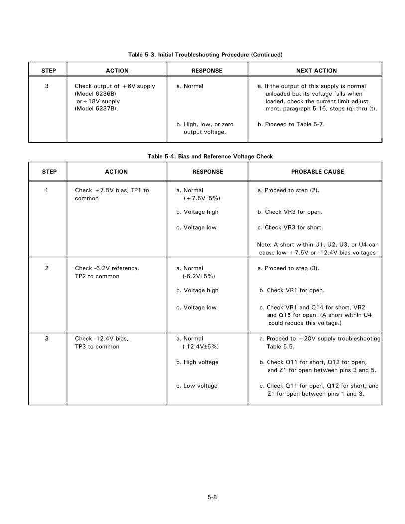
Table 5-3. Initial Troubleshooting Procedure (Continued)
STEP ACTION RESPONSE NEXT ACTION
3 Check output of +6V supply a. Normal a. If the output of this supply is normal (Model 6236B) unloaded but its voltage falls when or+18V supply loaded, check the current limit adjust (Model 6237B). ment, paragraph 5-16, steps (q) thru (t).
b. High, low, or zero b. Proceed to Table 5-7. output voltage.
Table 5-4. Bias and Reference Voltage Check
STEP ACTION RESPONSE PROBABLE CAUSE
1 Check +7.5V bias, TP1 to a. Normal a. Proceed to step (2). common (+7.5V±5%)
b. Voltage high b. Check VR3 for open.
c. Voltage low c. Check VR3 for short.
Note: A short within U1, U2, U3, or U4 cancause low +7.5V or -12.4V bias voltages
2 Check -6.2V reference, a. Normal a. Proceed to step (3). TP2 to common (-6.2V±5%)
b. Voltage high b. Check VR1 for open.
c. Voltage low c. Check VR1 and Q14 for short, VR2 and Q15 for open. (A short within U4
could reduce this voltage.)
3 Check -12.4V bias, a. Normal a. Proceed to +20V supply troubleshooting TP3 to common (-12.4V±5%) Table 5-5.
b. High voltage b. Check Q11 for short, Q12 for open, and Z1 for open between pins 3 and 5.
c. Low voltage c. Check Q11 for open, Q12 for short, and Z1 for open between pins 1 and 3.
5-8
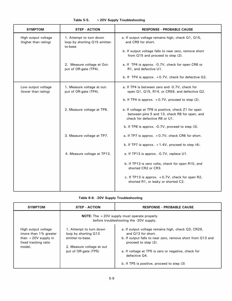
Table 5-5. +20V Supply Troubleshooting
SYMPTOM STEP - ACTION RESPONSE - PROBABLE CAUSE
High output voltage 1. Attempt to turn down a. If output voltage remains high, check Q1, Q15, (higher than rating) loop by shorting Q15 emitter- and CR9 for short.
to-base b. If output voltage falls to near zero, remove short
from Q15 and proceed to step (2).
2. Measure voltage at Out- a. If TP4 is approx. -0.7V, check for open CR6 orput of OR-gate (TP4). R1, and defective U1.
b. If TP4 is approx. +0.7V, check for defective Q2.
Low output voltage 1. Measure voltage at out- a. If TP4 is between zero and -0.7V, check for (lower than rating) put of OR-gate (TP4). open Q1, Q15, R14, or CR59, and defective Q2.
b. If TP4 is approx. +0.7V, proceed to step (2).
2. Measure voltage at TP8. a. If voltage at TP8 is positive, check Z1 for open between pins 5 and 13, check R8 for open, andcheck for defective R6 or U1.
b. If TP8 is approx. -0.7V, proceed to step (3).
3. Measure voltage at TP7. a. If TP7 is approx. +0.7V, check CR6 for short.
b. If TP7 is approx. +1.4V, proceed to step (4).
4. Measure voltage at TP13. a. If TP13 is approx. -0.7V, replace U1.
b. If TP13 is zero volts, check for open R10, and shorted CR2 or CR3.
c. If TP13 is approx. +0.7V, check for open R2, shorted R1, or leaky or shorted C2.
Table 6-6. -20V Supply Troubleshooting
SYMPTOM STEP - ACTION RESPONSE - PROBABLE CAUSE
NOTE: The +20V supply must operate properly before troubleshooting the -20V supply.
High output voltage 1. Attempt to turn down a. If output voltage remains high, check Q3, CR29,(more than 1% greater loop by shorting Q13 and Q13 for short.than +20V supply in emitter-to-base. b. If output falls to near zero, remove short from Q13 andfixed tracking ratio proceed to step (2).mode). 2. Measure voltage at out
put of OR-gate (TP5) a. If voltage at TP5 is zero or negative, check fordefective Q4.
b. If TP5 is positive, proceed to step (3)
5-9
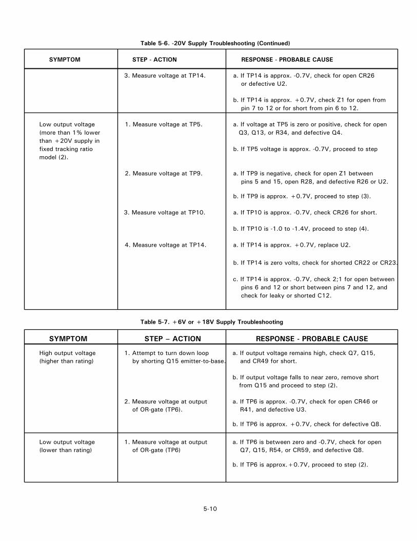
Table 5-6. -20V Supply Troubleshooting (Continued)
SYMPTOM STEP - ACTION RESPONSE - PROBABLE CAUSE
3. Measure voltage at TP14. a. If TP14 is approx. -0.7V, check for open CR26 or defective U2.
b. If TP14 is approx. +0.7V, check Z1 for open from pin 7 to 12 or for short from pin 6 to 12.
Low output voltage 1. Measure voltage at TP5. a. If voltage at TP5 is zero or positive, check for open(more than 1% lower Q3, Q13, or R34, and defective Q4.than +20V supply infixed tracking ratio b. If TP5 voltage is approx. -0.7V, proceed to stepmodel (2).
2. Measure voltage at TP9. a. If TP9 is negative, check for open Z1 between pins 5 and 15, open R28, and defective R26 or U2.
b. If TP9 is approx. +0.7V, proceed to step (3).
3. Measure voltage at TP10. a. If TP10 is approx. -0.7V, check CR26 for short.
b. If TP10 is -1.0 to -1.4V, proceed to step (4).
4. Measure voltage at TP14. a. If TP14 is approx. +0.7V, replace U2.
b. If TP14 is zero volts, check for shorted CR22 or CR23.
c. If TP14 is approx. -0.7V, check 2;1 for open between pins 6 and 12 or short between pins 7 and 12, and check for leaky or shorted C12.
Table 5-7. +6V or +18V Supply Troubleshooting
SYMPTOM STEP – ACTION RESPONSE - PROBABLE CAUSE
High output voltage 1. Attempt to turn down loop a. If output voltage remains high, check Q7, Q15,(higher than rating) by shorting Q15 emitter-to-base. and CR49 for short.
b. If output voltage falls to near zero, remove short from Q15 and proceed to step (2).
2. Measure voltage at output a. If TP6 is approx. -0.7V, check for open CR46 or of OR-gate (TP6). R41, and defective U3.
b. If TP6 is approx. +0.7V, check for defective Q8.
Low output voltage 1. Measure voltage at output a. If TP6 is between zero and -0.7V, check for open(lower than rating) of OR-gate (TP6) Q7, Q15, R54, or CR59, and defective Q8.
b. If TP6 is approx.+0.7V, proceed to step (2).
5-10
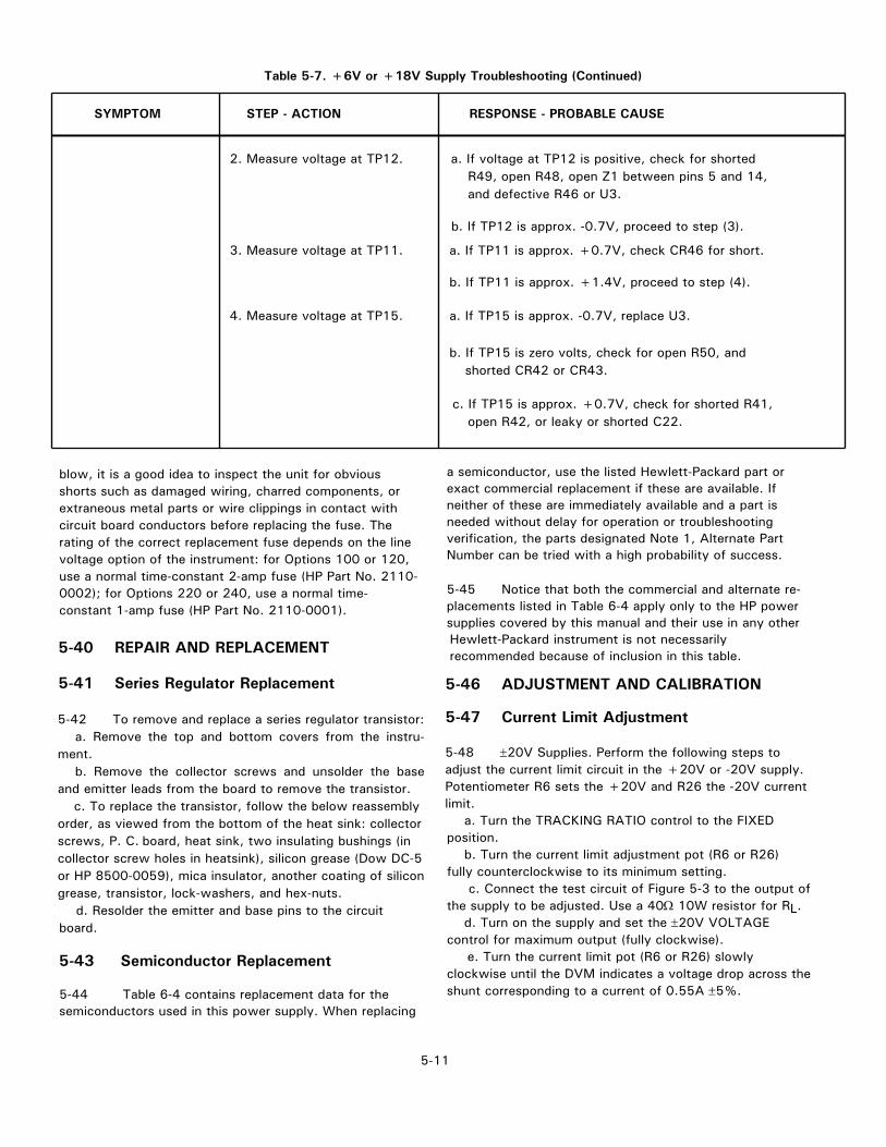
Table 5-7. +6V or +18V Supply Troubleshooting (Continued)
SYMPTOM STEP - ACTION RESPONSE - PROBABLE CAUSE
2. Measure voltage at TP12. a. If voltage at TP12 is positive, check for shorted R49, open R48, open Z1 between pins 5 and 14, and defective R46 or U3.
b. If TP12 is approx. -0.7V, proceed to step (3).
3. Measure voltage at TP11. a. If TP11 is approx. +0.7V, check CR46 for short.
b. If TP11 is approx. +1.4V, proceed to step (4).
4. Measure voltage at TP15. a. If TP15 is approx. -0.7V, replace U3.
b. If TP15 is zero volts, check for open R50, and shorted CR42 or CR43.
c. If TP15 is approx. +0.7V, check for shorted R41, open R42, or leaky or shorted C22.
blow, it is a good idea to inspect the unit for obviousshorts such as damaged wiring, charred components, orextraneous metal parts or wire clippings in contact withcircuit board conductors before replacing the fuse. Therating of the correct replacement fuse depends on the linevoltage option of the instrument: for Options 100 or 120,use a normal time-constant 2-amp fuse (HP Part No. 2110-0002); for Options 220 or 240, use a normal time-constant 1-amp fuse (HP Part No. 2110-0001).
5-40 REPAIR AND REPLACEMENT
5-41 Series Regulator Replacement
5-42 To remove and replace a series regulator transistor:a. Remove the top and bottom covers from the instru-
ment.b. Remove the collector screws and unsolder the base
and emitter leads from the board to remove the transistor. c. To replace the transistor, follow the below reassemblyorder, as viewed from the bottom of the heat sink: collectorscrews, P. C. board, heat sink, two insulating bushings (incollector screw holes in heatsink), silicon grease (Dow DC-5or HP 8500-0059), mica insulator, another coating of silicongrease, transistor, lock-washers, and hex-nuts.
d. Resolder the emitter and base pins to the circuitboard.
5-43 Semiconductor Replacement
5-44 Table 6-4 contains replacement data for thesemiconductors used in this power supply. When replacing
a semiconductor, use the listed Hewlett-Packard part orexact commercial replacement if these are available. Ifneither of these are immediately available and a part isneeded without delay for operation or troubleshootingverification, the parts designated Note 1, Alternate PartNumber can be tried with a high probability of success.
5-45 Notice that both the commercial and alternate re-placements listed in Table 6-4 apply only to the HP powersupplies covered by this manual and their use in any otherHewlett-Packard instrument is not necessarilyrecommended because of inclusion in this table.
5-46 ADJUSTMENT AND CALIBRATION
5-47 Current Limit Adjustment
5-48 ±20V Supplies. Perform the following steps toadjust the current limit circuit in the +20V or -20V supply.Potentiometer R6 sets the +20V and R26 the -20V currentlimit.
a. Turn the TRACKING RATIO control to the FIXEDposition.
b. Turn the current limit adjustment pot (R6 or R26)fully counterclockwise to its minimum setting. c. Connect the test circuit of Figure 5-3 to the output ofthe supply to be adjusted. Use a 40Ω 10W resistor for RL.
d. Turn on the supply and set the ±20V VOLTAGEcontrol for maximum output (fully clockwise).
e. Turn the current limit pot (R6 or R26) slowlyclockwise until the DVM indicates a voltage drop across theshunt corresponding to a current of 0.55A ±5%.
5-11
5-49 +6V Supply (Model 6236B). To adjust thecurrent limit circuit in the +6V supply, proceed as follows;
a. Check the setting of the current limit by performingsteps (r) and (s) of paragraph 5-16. (Be sure to set theoutput voltage to 6 volts.) If reducing the load resistancepermits the current to exceed 2.9A, stop, turn R46 slightlyclockwise, and repeat the test. If, instead, the currentbegins to fall before it reaches 2.6A, turn R46 slightlycounterclockwise and repeat the test.
b. Recheck the setting and readjust R46 until the testshows that the current limit circuit begins to reduce thecurrent when a decreasing load resistance increases it to2.75A ±5%.
5-50 +18V Supply (Model 6237B). To adjust thecurrent limit circuit in the +18V supply, proceed as follows:
a. Turn current limit adjustment pot (R46) fully clockwise to its minimum setting.
b. Connect the test circuit of Figure 5-3 to the outputof the +18V supply. Use an 18Ω 20W resistor for RL.
c. Turn on the supply and set the +18V VOLTAGEcontrol for maximum output (fully clockwise).
d. Turn current limit pot (R46) slowly counterclockwiseuntil the DVM indicates a voltage drop across the shuntcorresponding to a current of 1.1 A ±5%.
5-51 Meter Calibration
5-52 Panel Voltmeters. Check the accuracy of thepanel voltmeter by performing steps (a), (b), and (c) of theprocedure in paragraph 5-16. Since the same rangeresistors are used in both 20-volt ranges, their accuracy
will be the same. Adjust R58 so that the percentage errorin the +6V range (or +18V range) is equal to the error inthe 20-volt ranges. Turn R58 clockwise to increase theindications or counterclockwise to decrease them. If R58cannot calibrate all voltmeter ranges to within the ±4%specification, check the values of the resistors in thevoltmeter circuit.
5-53 Panel Ammeter. Check and calibrate the panelammeter by following the steps below.
a. Connect the test setup shown in Figure 5-3 to the+6V (or +18V) output. Make the total resistance of RLand the current sampling resistor 2.4 ohms (Model 6236B)or 18 ohms (6237B) to permit operating the supply at itsfull rated output. RL should have a power rating of at least20 watts.
b. Close the switch and set the +6V (+18V) VOLTAGEcontrol so that the DVM indicates an output of 2.5A(6236B) or 1.0A (6237B).
c. Check and record the panel ammeter accuracy on the+6V or +18V range.
d. Check each of the 20-volt ammeter ranges similarly,using the same test setup but making RL a 40Ω 10Wresistor and setting the voltage control for a 0.5A outputcurrent. Record the panel ammeter accuracy on each 20-voltrange.
e. Turn R59 clockwise to increase the indications on allthree ranges or counterclockwise to decrease them.
f. If R59 cannot calibrate all three ammeter ranges towithin the ±4% specification, check the values of the resis-tors in the circuit, including current monitoring resistors R8,R28, and R48.
5-12
SECTION VIREPLACEABLE PARTS
6-1 INTRODUCTION
6-2 This section contains information for ordering re-placement parts. Table 6-4 lists parts in alpha-numericorder by reference designators and provides the followinginformation:
a. Reference Designators. Refer to Table 6-1.b. Description. Refer to Table 6-2 for abreviations.c. Total Quantity (TQ). Given only the first time
the part number is listed except in instruments containingmany sub-modular assemblies, in which case the TQ appearsthe first time the part number is listed in each assembly.
d. Manufacturer's Part Number or Type.e. Manufacturer's Federal Supply Code Number.
Refer to Table 6-3 for manufacturer's name and address.f. Hewlett-Packard Part Number.g. Recommended Spare Parts Quantity (RS) for
complete maintenance of one instrument during one year ofisolated service.
h. Parts not identified by a reference designator arelisted at the end of Table 6-4 under Mechanical and /orMiscellaneous. The former consists of parts belonging to andgrouped by individual assemblies; the latter consists of allparts not immediately associated with an assembly.
6-3 ORDERING INFORMATION
6-4 To order a replacement part, address order or in-quiry to your local Hewlett-Packard sales office (see listsat rear of this manual for addresses). Specify thefollowing information for each part: Model, complete serialnumber, and any Option or special modification (J)numbers of the instrument; Hewlett-Packard part number;circuit reference designator; and description. To order apart not listed in Table 6-4, give a complete description ofthe part, its function, and its location.
Table 6-1. Reference Designators (Continued)
Table 6-2. Description Abbreviations
6-1
Table 6-1. Reference Designators
A = assembly E = miscellaneous B = blower (fan) electronic part C = capacitor F = fuse CB = circuit breaker J = jack, jumper CR = diode K = relay DS = device, signaling L = inductor
(lamp) M = meter
P = plug V = vacuum tube, Q = transistor neon bulb, R = resistor photocell, etc. S = switch VR = zener diode T = transformer X = socket. TB = terminal block Z = integrated cir- TS = thermal switch cuit or network
A = ampere mod. = modular orAc = alternating current modifiedassy. = assembly mtg = mountingbd = board n = nano = 10-9bkt = bracket NC = normally closed°C = degree Centigrade NO = normally opencd = card NP = nickel-platedcoef = coefficient Ω = ohmcomp = composition obd = order byCRT = cathode-ray tube descriptionCT = center-tapped OD = outside diameterdc = direct current p = pico=1012
DPDT = double pole, P.C. = printed circuit double throw pot. = potentiometer
DPST = double pole, p-p = peak-to-peak single throw ppm = parts per millionelect = electrolytic pvr = peak reverseencap = encapsulated voltageF = farad rect = rectifier°F = degree Farenheit rms = root mean square
fxd = fixed Si = siliconGe = germanium SPDT = single pole,H = Henry double throwHz = Hertz SPST = single pole,IC = integrated circuit single throwID = inside diameter SS = small signalincnd = incandescent T = slow-blowk = kilo = 103 tan. = tantalumm = milli = 10-3 Ti = titaniumM = mega = 106 V = voltµ = micro = 10-6 var = variablemet. = metal ww = wirewoundmfr = manufacturer W = Watt
Table 6-3. Code List of Manufacturers
6-2
CODE MANUFACTURER ADDRESS
01121 Allen Bradley Co. Milwaukee, WI02114 Ferroxcube Corp. Saugerties, NY02582 Clarostat Mfg. Co., Inc. Dover, NH02735 Radio Corp. of America, Solid State and Receiving Tube Div. Somerville, NJ03508 G. E. Semiconductor
Products Dept. Syracuse, NY04200 Sprague Electric Co. North Adams, MA04713 Motorola Semiconductor
Prod. Inc. Phoenix, AZ05524 Dale Electronics Inc. Columbus, NE05820 Wakefield Engr. Inc. Wakefield, MA05917 Aktiebolaget Rifa Bromma, Sweden07716 IRC Div. of TRW Inc. Burlington, IA
CODE MANUFACTURER ADDRESS
09353 C & K Components Inc. Newton, MA19701 Electra/Midland Corp. Mineral Wells, TX27014 National Semiconductor
Corp. Santa Clara, CA28480 Hewlett-Packard Co. Palo Alto, CA61637 Union Carbide Corp. New York, NY71450 CTS Corp. Elkhart, IN72136 Electro Motive Mfg.Co., Inc.
Willimantic, CT75042 IRC Div. of TRW, Inc. Philadelphia, PA75915 Littlefuse,Inc. DesPlaines,IL
Table 6-4. Replaceable Parts
* 6236B/6237B6-3
REF. MFR. MFR. HP DESIG. DESCRIPTION TQ* PART NO. CODE PART NO. RS
Printed Circuit Board Assy.C1 fxd, elect 180µF 50V 2/3 672D047 04200 0180-0634 1C2 fxd, tant 6.8µF 35V 3 150D685X9035B2 04200 0180-0116 1C3, 4 fxd, polyester 2200pF 200V 2 292P22292-PTS 04200 0160-0154 1C7 fxd, elect 1450µF 45V 2 (Type68D) D39532 04200 0180-1893 1C8, 9 fxd, cer .05µF 400V 6/4 33C17A3-CDH 04200 0150-0052 1C11 fxd, elect 180µF 50V 672D047 04200 0180-0634C12 fxd, tant 6.8µF 35V 150D685X9035B2 04200 0180-0116C13 fxd, polyester .01µF 200V 2 292P10392-PTS 04200 0160-0161 1C14 fxd, polyester 3300pF 200V 1 292P33292-PTS 04200 0160-0155 1C17 fxd, elect 1450µF 45V (Type 68D) D39532 04200 0180-1893C18, 19 fxd, cer .05µF 400V 33C17A3-CDH 04200 0150-0052C21
6236B fxd, elect 1000µF 12V 1 627D046 04200 0180-0633 16237B fxd, elect 180µF 50V 672D047 04200 0180-0634
C22 fxd, tant 6.8µF 35V 150D685X9035B2 04200 0180-0116C23 fxd, cer .005µF 100V 1 C023B101E502MS27 04200 0160-2639 1C24 fxd, polyester .01µF 200V 292P10392-PTS 04200 0160-0161C27
6236B fxd, elect 5600µF 25V 1 (Type 32D) D40018 04200 0180-1921 16237B fxd, elect 3000µF 40V 1 32D5278-DQB 04200 0180-1899 1
C28, 296236B fxd, cer .05µF 400V 33C17A3-CDH 04200 0150-00526237B Not used
C306236B Not used6237B fxd, cer 0.1µF 500V 1 41C92B5-CDH 04200 0160-0269 1
C316236B fxd, tant 0.47µF 35V 1 150D474X9035A2 04200 0180-0376 16237B fxd, elect 0.15µF 35V 1 T110A154K035AS 61637 0180-0218 1
C32 fxd, mica 330pF 500V 1 obd 72136 0160-2012 1C33 fxd, elect 490µF 85V 1 (Type 68D) D38618 04200 0180-1888 1C34 fxd, paper 0.1µF 250Vac 1 PME271-M-610 05917 0160-4065 1CR1 Diode, Si 1A 200V 13/15 1N5059 1901-0327 7CR2-7 Diode, Si 17 1N485B 1901-0033 7CR9, 11, 12, 21 Diode, Si 1A 200V 1N5059 1901-0327CR22-26 Diode, Si 1N485B 1901-0033CR28,29,31,32 Diode, Si 1A 200V 1N5059 1901-0327CR41 Diode, Si 1.5A 200V 3 1N4999 1901-0416 3CR42, 43 Diode, Si 1N485B 1901-0033CR44 Diode, stabistor 150mA 15V 2 STB523 03508 1901-0460 2CR45-47 Diode, Si 1N485B 1901-0033CR49 Diode, Si 1A 200V 1N5059 1901-0327CR51, 52 Diode, Si 1.5A 200V 1N4999 1901-0416CR53, 54
6236B Not used6237B Diode, Si 1A 200V 1N5059 1901-0327
CR55, 56 Diode, Si 1A 200V 1N5059 1901-0327CR57 Diode, stabistor 150mA 15V STB523 03508 1901-0460CR59 Diode, Si 1A 200V 1N5059 1901-0327
Table 6-4. Replaceable Parts (Continued)
Note 1: Alternate part number. See para. 5-43. 6-4
REF. MFR. MFR. HP DESIG. DESCRIPTION TQ* PART NO. CODE PART NO. RS
CR60 Diode, Si 1N485B 1901-0033L1, 2, 3 Inductor, ferrite bead 3 56-590-65/4A6 02114 9170-0894 1
(Q2, Q3, CR49)Q2 SS NPN Si 3 SS1147 (Note1) 04713 1854-0448 3Q4 SS PNP Si 1 2N2904A 1853-0012 1Q11 Power PNP Si 1 2N3740 1853-0052 1Q12 SS NPN Si SS1147 (Note 1) 04713 1854-0448Q13 SS PNP Si 1 2N4036 1853-0041 1Q14 SS NPN Si 1 2N2714A 1854-0027 1Q15 SS NPN Si SS1147 (Note 1) 04713 1854-0448R1 var. 10k (VOLTAGE ±20V) 2 43X 02582 2100-3461R2 fxd, film 2.61k 1% 1/8W 1 Type MF4C, T-9 19701 0698-0092 1R3 fxd, ww 0.1 10% 3W 2 RS-2B 05524 0811-1827 1R4 fxd, comp 18 5% 1/2W 3 EB1805 01121 0686-1805 1R6 var. ww 3k 3 Type 110-F4 71450 2100-1823 1R8 fxd, ww 1.25 1/2% 5W 2 RS5 05524 0811-3384 1R9 fxd, film 5.49k 1% 1/8W 1 Type MF4C, T-0 19701 0698-3382 1R10 fxd, film 1.5k 1% 1/8W 1 Type MF4C, T-0 19701 0757-0427 1R11 fxd, film 110k 1% 1/8W 2 Type MF4C, T-0 19701 0757-0466 1R12 fxd, film 139 1% 1/8W 3 Type CEA, T-0 07716 0698-4099 1R13 fxd, comp 15k 5% 1/2W 1 EB 1535 01121 0686-1535 1R14 fxd, comp 510 5% 1W 1 GB5115 01121 0689-5115 1R15 fxd, comp 10k 5% 1/2W 2 EB1035 01121 0686-1035 1R23 fxd, ww 0.25 10% 3W 1 RS-2B 05524 0811-1829 1R24 fxd, comp 18 5% 1/2W EB1805 01121 0686-1805R26 var. ww 3k Type 110-F4 71450 2100-1823R28 fxd, ww 1.25 1/2% 5W RS5 05524 0811-3384R32 fxd, film 139 1% 1/8W Type CEA, T-0 07716 0698-4099R33 fxd, film 15k 1% 1/8W 2 Type MF4C, T-0 19701 0757-0446 1R34 fxd, comp 510 5% 1/2W 1 EB5115 01121 0686-5115 1R35 fxd, comp 10k 5% 1/2W EB1035 01121 0686-1035R41 var, 10k 43X 02582 2100-3461
(VOLTAGE +6V or +18V)R42
6236B fxd, film 8.66k 1% 1/8W 1 Type MF4C, T-9 19701 0698-8076 16237B fxd, film 2.87k 1% 1/8W 1 Type MF4C-1 19701 0698-7631 1
R43 fxd, ww 0.1 10% 3W RS-2B 05524 0811-1827R44 fxd, comp 18 5% 1/2W EB1805 01121 0686-1805R45
6236B Not used6237B fxd, film 2k 1% 1/8W 1 CEA993 07716 0757-0283 1
R46 var. ww 3k Type 110-F4 71450 2100-1823R47
6236B fxd, film 23k 1% 1/8W 1 Type MF4C, T-0 19701 0698-3269 16237B Not used
R486236B fxd, ww 0.25 1/2% 5W 1 RS5 05524 0811-3383 16237B. fxd, ww 0.625 1/2% 5W 1 RS5 05524 0811-3395 1
R496236B fxd, film 750 1% 1/8W 1 Type MF4C, T-0 19701 0757-0420 16237B Not used
Table 6-4. Replaceable Parts (Continued)
Note 1: Alternate part number. See para. 5-43.
REF. MFR. MFR. HP DESIG. DESCRIPTION TQ* PART NO. CODE PART NO. RS
R506236B fxd, film 330 1% 1/8W 1 Type MF4C, T-9 19701 0698-5663 16237B fxd, film 3.83k 1% 1/8W 1 Type MF4C-1 19701 0698-3153 1
R51 fxd, film 110k 1% 1/8W Type MF4C, T-0 19701 0757-0466R52 fxd, film 139 1% 1/8W Type CEA, T-0 07716 0698-4099R53 fxd, comp 7.5k 5% 1/2W 1 EB7525 01121 0686-7525 1R54
6236B fxd, ww 50 5% 10W 1 Type 247E 04200 0811-1902 16237B fxd, ww 135 5% 10W 1 Type 247E 04200 0811-1905 1
R556236B fxd, comp 2.2k 5% 1/2W 1 EB2225 01121 0686-2225 16237B fxd, comp 11k 5% 1/2W 1 EB1135 01121 0686-1135 1
R56 fxd, film 270 1% 1/8W 1 Type CEA, T-0 07716 0757-0269 1R57 fxd, film 221k 1% 1/8W 1 Type MF4C, T-0 19701 0757-0473 1R58,59 var. ww 250 2 Type 110 71450 2100-0439 1R60 fxd, film 15k 1% 1/8W Type MF4C, T-0 19701 0757-0446R61 fxd, comp 240 5% 1/2W 1 EB2415 01121 0686-2415 1R62 fxd, film 11k 1% 1/8W 2 Type MF4C, T-0 19701 0757-0443 1R63 fxd, film 3.6k 2% 1/8W 1 Type MF4C, T-0 19701 0757-0937 1R64 fxd, film 11k 1% 1/8W Type MF4C, T-0 19701 0757-0443R65 fxd, film 16.2k 1% 1/8W 1 Type MF4C, T-0 19701 0757-0447 1R66 fxd, film 470 1% 1/4W 1 Type MF52C, T-0 19701 0698-3506 1R67
6236B fxd, ww 135 5% 3W 1 Type 242E 04200 0812-0112 16237B fxd, ww 220 5% 2W 1 Type BWH 75042 0811-1763 1
R686236B fxd, ww 250 5% 3W 1 Type 242E 04200 0811-1219 16237B fxd, ww 490 5% 3W 1 Type 242E 04200 0811-1801 1
R696236B fxd, ww 100 5% 10W 1 Type 247E 04200 0811-1903 16237B fxd, ww 150 5% 10W 1 Type 247E 04200 0811-1906 1
R70
6236B fxd, ww 40 5% 5W 1 Type 243E 04200 0812-0083 1
6237B fxd, ww 75 5% 5W 1 RS5 05524 0812-0097 1
R71 fxd, film 471 1% 1/8W 1 Type CMF-55-1, T-1 05524 0698-5514 1R72 fxd, comp 33k 5% 1/2W 1 EB3335 01121 0686-3335 1R73,6236B Not used
6237B fxd,comp 1.1M 5% 1/2W 1 EB1155 01121 0686-1155 1R74,6236B (jumper installed)
6237B fxd, film 6.98k 1% 1/8W 1 Type CMF-55-1, T-1 05524 0698-4470 1
R76 fxd, ww 10k 5% 3W 1 RS-2B 05524 0811-1816 1S3 slide switch, dual DPDT 1 28480 3101-1914 1T1 Power Transformer 28480 06236-80091U1-3 Dual op amp, IC 3 CA 3458T (Note 1) 02735 1826-0092 3
U4 Operational amp, IC 1 LM301AH 27014 1820-0223 1VR1 Diode, zener 6.2V 1 1N825 1902-1221 1VR2 Diode, zener 9.09V 1 SZ10939-170 04713 1902-3149 1VR3 Diode, zener 7.5V 1 1N4353B 1902-0650 1Z1 Resistor network 1 28480 1810-0217
1
6-5
Table 6-4. Replaceable Parts (Continued)
Note 1: Alternate part number. See para. 5-43.
6-6
REF. MFR. MFR. HP DESIG. DESCRIPTION TQ* PART NO. CODE PART NO. RS
Front Panel - ElectricalDS1 Indicator light, LINE ON 1 28480 1450-0566 1M1
6236B Voltmeter, 0-25V 1 28480 1120-1380 16237B Voltmeter, 0-25V 1 28480 1120-1382 1
M26236B Ammeter, 0-3A 1 28480 1120-1381 16237B Ammeter, 0-1.2A 1 28480 1120-1383 1
S1 Toggle Switch, LINE ON 1 7318-PHI 09353 3101-1694 1S2 3-pos. rotary switch, METER 1 28480 3100-1943 1
R77 var. 10k (TRACKING RATIO) 1 28480 2100-3656Rear Heatsink - Electrical
F1 Fuse, 2A 250V (Std. Option and Option 100) 1 312002 75915 2110-0002 5
F1 Fuse, 1 A 250V (Options 220 and 240) 1 312001 75915 2110-0001 5
Q1, 7 Power PNP Si 2 SJ1528 04713 1853-0063 2Q3, 8 Power NPN Si 2 2N3055 (Note 1) 1854-0563 2
Circuit Board - MechanicalHeat Dissipator (CR51, 52, Q2,Q11 in 6236B; Q2 in 6237B) 4/1 207-CB 05820 1205-0033Heat Sink (Q11) 1 28480 5000-6025Spacer (for Q11 heatsink) 2 28480 0380-0004Rubber bumper 4 28480 0403-0086
Front Panel - MechanicalBinding Post, red 4 28480 1510-0091Binding Post, black 1 28480 1510-0107 Meter bezel 2 28480 4040-0571Spring, compression 8 28480 1460-0720(meter mount)Retainer, push-on (for DSI) 1 28480 0510-0123Knob (R1, R41, R77, S2) 4 28480 0370-1099
MiscellaneousBushing, transistor insulator 8 28480 0340-0168Transistor insulator, mica 4 28480 0340-0174Fuse holder 1 342014 75915 1400-0084Lockwasher, fuseholder 1 28480 2190-0054Nut, nylon 1/2 - 24 1 28480 2950-0131Foot, rubber 4 28480 0403-0088Line cord strain relief 1 28480 0400-0013Line cord 1 see par. 2-21Chassis assembly, left 1 28480 5060-7955Chassis assembly, right 1 28480 5060-7956Front panel (6236B) 1 28480 06236-00001Front panel (6237B) 1 28480 06237-00001Heat sink, rear 1 28480 5020-8423Cover, top and bottom 2 28480 5000-9424Packing carton 1 28480 9211-2518Floater pad, packing carton 2 28480 9220-1218
APPENDIX AMANUAL BACKDATING CHANGES
To adapt this manual to Model 6236A or 6237A instruments, make the changes indicated in the table below.
CHANGE 1 :Delete R76, R77, and all references to the variable tracking
ratio feature.
CHANGE 2:Change potentiometers R1 and R41 to 10kΩ panel-mounted
type, HP Part No. 2100-1854.
CHANGE 3:Delete ferrite bead L3, 9170-0894, from the lead of diode
CR49.
A-1
MODEL SERIAL NUMBERS MAKE CHANGES
6236A ALL 1 1507A-00141 thru -00350 2 1436A-00101 thru -00127 3
6237A ALL 1 1511A-00101 thru -00170 2
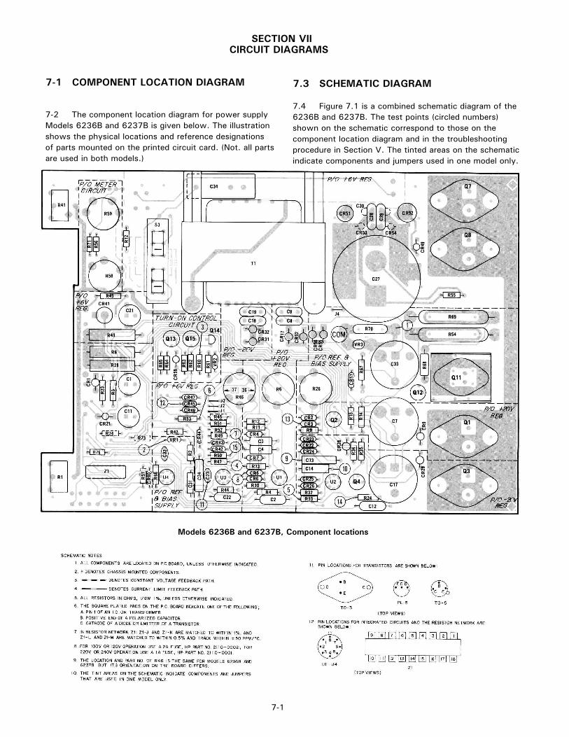
SECTION VIICIRCUIT DIAGRAMS
7-2 The component location diagram for power supplyModels 6236B and 6237B is given below. The illustrationshows the physical locations and reference designationsof parts mounted on the printed circuit card. (Not. all partsare used in both models.)
7.4 Figure 7.1 is a combined schematic diagram of the6236B and 6237B. The test points (circled numbers)shown on the schematic correspond to those on thecomponent location diagram and in the troubleshootingprocedure in Section V. The tinted areas on the schematicindicate components and jumpers used in one model only.
Models 6236B and 6237B, Component locations
7-1
7.3 SCHEMATIC DIAGRAM7-1 COMPONENT LOCATION DIAGRAM
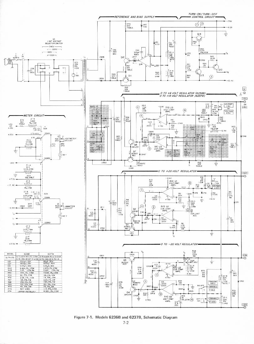
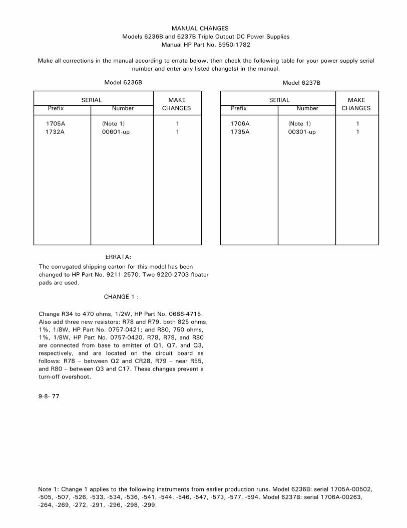
MANUAL CHANGESModels 6236B and 6237B Triple Output DC Power Supplies
Manual HP Part No. 5950-1782
Make all corrections in the manual according to errata below, then check the following table for your power supply serialnumber and enter any listed change(s) in the manual.
Model 6236B
ERRATA:
The corrugated shipping carton for this model has beenchanged to HP Part No. 9211-2570. Two 9220-2703 floaterpads are used.
CHANGE 1 :
Change R34 to 470 ohms, 1/2W, HP Part No. 0686-4715.Also add three new resistors: R78 and R79, both 825 ohms,1%, 1/8W, HP Part No. 0757-0421; and R80, 750 ohms,1%, 1/8W, HP Part No. 0757-0420. R78, R79, and R80are connected from base to emitter of Q1, Q7, and Q3,respectively, and are located on the circuit board asfollows: R78 − between Q2 and CR28, R79 − near R55,and R80 − between Q3 and C17. These changes prevent aturn-off overshoot.
9-8- 77
Model 6237B
Note 1: Change 1 applies to the following instruments from earlier production runs. Model 6236B: serial 1705A-00502,-505, -507, -526, -533, -534, -536, -541, -544, -546, -547, -573, -577, -594. Model 6237B: serial 1706A-00263,-264, -269, -272, -291, -296, -298, -299.
SERIAL MAKE SERIAL MAKEPrefix Number CHANGES Prefix Number CHANGES
1705A (Note 1) 1 1706A (Note 1) 1 1732A 00601-up 1 1735A 00301-up 1