Embed Size (px)
Citation preview

Managing Director:
Volker Keith & Dipl.-Phys. Ing. Luitger Koep
Rev.1.3
Technical modifications reserved,
errors excepted
www.keith-koep.com
- 1 of 32 -
Keith & Koep GmbH
Uellendahler Str. 199
42109 Wuppertal
Tel. +49 (202) 25253-0
Fax +49 (202) 25253-33
Trizeps VIII Mini
Documentation version 1.8
Front Back
Introduction
The Trizeps VIII Mini is powered by NXP i.MX 8M Mini processor, which is designed to meet the
latest market requirements of connected streaming audio/video devices, scanning/imaging devices
and various devices demanding high-performance and low-power.
The i.MX 8M Mini family of processors features advanced implementation of a quad ARM® Cortex®
A53 core, which operates at speeds of up to 1.8GHz (consumer version) and 1.6GHz (industrial
version).
A general purpose Cortex®-M4 core processor is for low-power processing. A 32-bit LPDDR4 is used
for memory. There are a number of other i.MX 8M Mini interfaces for connecting peripherals, such
as displays, cameras, GPS and sensors, which are extended by components already available on
the module:
• a stereo, hi-fi quality audio-codec.
• a FPGA with up to 4300 LUT to convert parallel display/camera/data-streams to/from MIPI
and for user defined programmable logic.
• a programmable Cortex-M0 for realtime processing, capable of reading multiple 16bit
analog inputs, usable as resistive touch-controller and for CAN communication.
• WLAN 802.11 a/b/g/n/ac and Bluetooth 4.2 and 5 ready module
SODIMM Standard
The Trizeps VIII Mini features the Keith & Koep SODIMM 200 Standard, the world‘s longest existing
SODIMM standard. Like no other module standard, the SODIMM 200 ensures the pin compatibility
of the Trizeps modules.
The main difference of the Trizeps VIII Mini is the missing address/data bus, which is no longer
supported by the i.MX 8M Mini CPU. The pins, which are no longer needed for this function, are
used for GBit Ethernet signals. Trizeps VIII Mini and Trizeps VIII are mostly pin compatible.

- 2 of 32 -
Block Diagram
Figure 0-1: Simplified Block Diagram of Trizeps VIII Mini
The Trizeps VIII Mini module got a SODIMM200 card edge connector and a 60pin FX11 high-speed
board connector. The pinning of both connectors is to a large extent compatible to previous Trizeps
modules.

- 3 of 32 -
Features and Interfaces
Features
Processor:
NXP i.MX 8M Mini ARM® Quad Cortex-A53 at up to 1.8GHz (consumer), 1.6GHz (industrial)
NXP i.MX 8M Mini ARM® Cortex-M4
NXP Kinetis V ARM® Cortex-M0+ at up to 75MHz
Memory:
1 or 2 GByte of 32-bit LPDDR4-3200
Higher densities are available on request.
Storage:
Micro-SD socket
or
4 or 8 GByte eMMC
Higher densities are available on request.
Wireless:
WLAN 802.11 a/b/g/n/ac
Bluetooth 4.2 and Bluetooth 5.0 ready
Micro RF-antenna connector
Power:
PMIC to generate all internal and external voltages from 3.3V supply.
Dimensions:
(Length x Width x Height): 67.6 x 36.7 x 6.4 mm
Interfaces / Signals accessible over connectors – Power Supply through +3.3V.
– 2x USB2.0 OTG port (USB Host or Slave).
– PCIe
– SD/SDIO Card Interface
– 4x UART
– SPI and Quad-SPI
– 2x I2C
– Mipi Display (4ch) or Single/Dual LVDS or parallel RGB Display.
– 1x Mipi Camera (4ch).
– 1Gbit,100/10Mbit Ethernet
– 1x CAN
– 2x 4ch 16bit ADC
– Stereo Headphone
– Stereo Line-In
– Microphone input
– 1W Speaker output
– SPDIF In and Out
– Multi-Channel Serial-Audio-Interface
– GPIO, PWM

- 4 of 32 -
1 Pin-Description
The main connector of the Trizeps VIII Mini is the SODIMM200 connector.
To operate, only +3V3 and GND pins need to be connected. Leave unused pins unconnected.
The U14 Board2Board connector can be omitted if the signals are not needed.
J1 and J2 may be used for debugging, programming and testing.
On the bottom side are UFL antenna connectors for the on-board WLAN + Bluetooth chip.
J2: FPGA and MCU JTAG
J1: i.MX 8M Mini JTAG U14: Board2Board Connector
U4: SODIMM
Figure 1-1: Connectors
1.1 Pin-Description (Primary Function)
The i.MX8M Mini processor, the Cortex M0+ MCU and the FPGA are highly configurable devices,
where each pin may have multiple different functions.
The pin-names are derived from previous Trizeps-versions and their primary or most interesting
function.
Please view chapter “1.2 Pin-Mux Information” for details on how these pins may be configured by
software.
Notes:
*1) In the table below, some of the old Trizeps pin-names are placed in brackets [] for reference.
*2) FPGA_CIF_D[9..0] / SAIx_RXD[7..0], FPGA_CIF_HSYNC, FPGA_CIF_MCLK and
FPGA_CIF_PCLK are routed to the FPGA and the i.MX 8M. In the following documentation they are
either named FPGA_CIF_Dx or SAIx_RXDy, depending if the FPGA or i.MX 8M function is described.
*3) FPGA_CIF_VSYNC, FPGA_CIF_HSYNC, FPGA_CIF_MCLK and FPGA_CIF_PCLK are connected to
i.MX 8M pins, if the FPGA is not mounted (RA3).
*4) BT_PCM_IN, BT_PCM_OUT, BT_PCM_SYNC and BT_PCM_CLK are connected to the on-board
Bluetooth-module if it is mounted!
*5) PCIE_CLKREQ may not be usable when Wifi module is mounted.

- 5 of 32 -
J500: SODIMM Connector
Signal Pin Pin Signal
AUDIO_MIC_OUT 1 2 VIN_AD3 (MCU)
AUDIO_MIC_GND 3 4 VIN_AD2 (MCU)
AUDIO_LINEIN_L 5 6 VIN_AD1 (MCU)
AUDIO_LINEIN_R 7 8 VIN_AD0 (MCU)
AUDIO_AGND 9 10 AUDIO_VDDA
AUDIO_AGND 11 12 AUDIO_VDD_SPEAKER
AUDIO_HEADPHONE_GND 13 14 TSPX (MCU)
AUDIO_HEADPHONE_L 15 16 TSMX (MCU)
AUDIO_HEADPHONE_R 17 18 TSPY (MCU)
UART3_RXD 19 20 TSMY (MCU)
UART3_TXD 21 22 SPIN22_RTS3
UART1_DTR 23 24 SPIN24_CTS3
UART1_CTS 25 26 RESET_IN
UART1_RTS 27 28 SPEAKER_R
UART1_DSR 29 30 SPEAKER_L
UART1_DCD 31 32 UART2_CTS
UART1_RXD 33 34 UART2_RTS
UART1_TXD 35 36 UART2_RXD
UART1_RI 37 38 UART2_TXD
GND 39 40 VCC (+3V3)
GND 41 42 VCC (+3V3)
SPIN43 43 44 FPGA_LCD_DE
SPIN45 45 46 FPGA_LCD_D07
SD2_CLK 47 48 FPGA_LCD_D09
FPGA_CIF_D0 / SAI1_RXD0 49 50 FPGA_LCD_D11
SD2_DATA3 51 52 FPGA_LCD_D12
FPGA_CIF_D1 / SAI1_RXD1 53 54 FPGA_LCD_D13
SPIN55 55 56 FPGA_LCD_PCLK
FPGA_CIF_D2 / SAI1_RXD2 57 58 FPGA_LCD_D03
SD2_DETECT 59 60 FPGA_LCD_D02
FPGA_CIF_D3 / SAI1_RXD3 61 62 FPGA_LCD_D08
FPGA_CIF_D4 / SAI1_RXD4 63 64 FPGA_LCD_D15
FPGA_CIF_D5 / SAI1_RXD5 65 66 FPGA_LCD_D14
FPGA_CIF_D6 / SAI1_RXD6 67 68 FPGA_LCD_HSYNC
LED_GPIO 69 70 FPGA_LCD_D01
FPGA_CIF_D7 / SAI1_RXD7 71 72 FPGA_LCD_D05
FPGA_CIF_D8 / SAI5_RXD1 73 74 FPGA_LCD_D10
FPGA_CIF_D9 / SAI5_RXD2 75 76 FPGA_LCD_D00
BACKLIGHT_PWM 77 78 FPGA_LCD_D04
POWERFAIL 79 80 FPGA_LCD_D06
SD2_DATA1 81 82 FPGA_LCD_VSYNC
GND 83 84 VCC (+3V3)
SD2_DATA2 85 86 FPGA_CIF_VSYNC (*3)
RESET_OUT 87 88 FPGA_CIF_MCLK / SAI1_MCLK (*3)
+3V3_AUX 89 90 FPGA_CIF_PCLK / SAI1_RXC (*3)
+3V3_AUX 91 92 FPGA_CIF_HSYNC / SAI1_RXFS (*3)
SPIN93 [RD/WR] 93 94 I2C1_SCL
SPIN95 [RDY] 95 96 I2C1_SDA
CAN1_RX (MCU) 97 98 GPIO_AUX
CAN1_TX (MCU) 99 100 DISPLAY_ENABLE
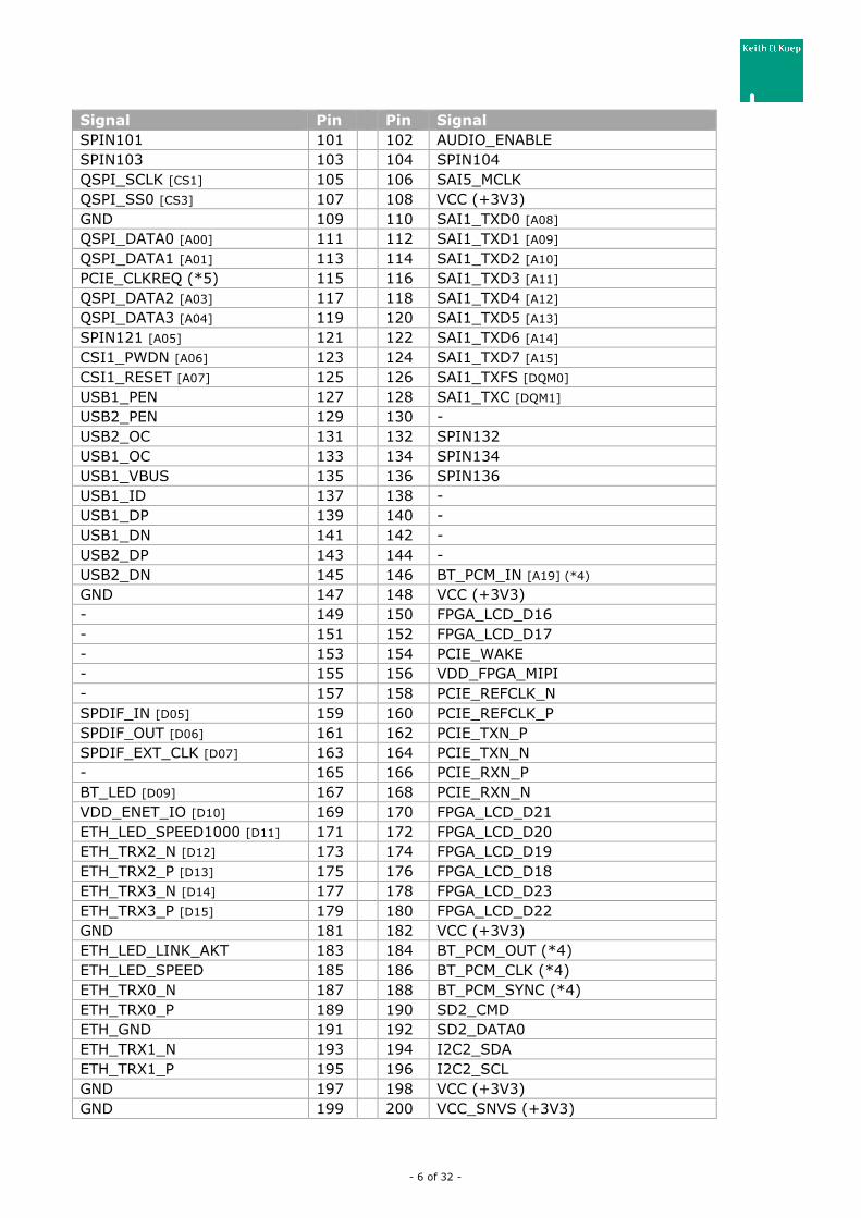
- 6 of 32 -
Signal Pin Pin Signal
SPIN101 101 102 AUDIO_ENABLE
SPIN103 103 104 SPIN104
QSPI_SCLK [CS1] 105 106 SAI5_MCLK
QSPI_SS0 [CS3] 107 108 VCC (+3V3)
GND 109 110 SAI1_TXD0 [A08]
QSPI_DATA0 [A00] 111 112 SAI1_TXD1 [A09]
QSPI_DATA1 [A01] 113 114 SAI1_TXD2 [A10]
PCIE_CLKREQ (*5) 115 116 SAI1_TXD3 [A11]
QSPI_DATA2 [A03] 117 118 SAI1_TXD4 [A12]
QSPI_DATA3 [A04] 119 120 SAI1_TXD5 [A13]
SPIN121 [A05] 121 122 SAI1_TXD6 [A14]
CSI1_PWDN [A06] 123 124 SAI1_TXD7 [A15]
CSI1_RESET [A07] 125 126 SAI1_TXFS [DQM0]
USB1_PEN 127 128 SAI1_TXC [DQM1]
USB2_PEN 129 130 -
USB2_OC 131 132 SPIN132
USB1_OC 133 134 SPIN134
USB1_VBUS 135 136 SPIN136
USB1_ID 137 138 -
USB1_DP 139 140 -
USB1_DN 141 142 -
USB2_DP 143 144 -
USB2_DN 145 146 BT_PCM_IN [A19] (*4)
GND 147 148 VCC (+3V3)
- 149 150 FPGA_LCD_D16
- 151 152 FPGA_LCD_D17
- 153 154 PCIE_WAKE
- 155 156 VDD_FPGA_MIPI
- 157 158 PCIE_REFCLK_N
SPDIF_IN [D05] 159 160 PCIE_REFCLK_P
SPDIF_OUT [D06] 161 162 PCIE_TXN_P
SPDIF_EXT_CLK [D07] 163 164 PCIE_TXN_N
- 165 166 PCIE_RXN_P
BT_LED [D09] 167 168 PCIE_RXN_N
VDD_ENET_IO [D10] 169 170 FPGA_LCD_D21
ETH_LED_SPEED1000 [D11] 171 172 FPGA_LCD_D20
ETH_TRX2_N [D12] 173 174 FPGA_LCD_D19
ETH_TRX2_P [D13] 175 176 FPGA_LCD_D18
ETH_TRX3_N [D14] 177 178 FPGA_LCD_D23
ETH_TRX3_P [D15] 179 180 FPGA_LCD_D22
GND 181 182 VCC (+3V3)
ETH_LED_LINK_AKT 183 184 BT_PCM_OUT (*4)
ETH_LED_SPEED 185 186 BT_PCM_CLK (*4)
ETH_TRX0_N 187 188 BT_PCM_SYNC (*4)
ETH_TRX0_P 189 190 SD2_CMD
ETH_GND 191 192 SD2_DATA0
ETH_TRX1_N 193 194 I2C2_SDA
ETH_TRX1_P 195 196 I2C2_SCL
GND 197 198 VCC (+3V3)
GND 199 200 VCC_SNVS (+3V3)

- 7 of 32 -
J400: Board2Board Connector
Signal Pin Pin Signal
MIPI_CSI1_D2_P 1 2 ETH_SI_N
MIPI_CSI1_D2_N 3 4 ETH_SI_P
MIPI_CSI1_D3_P 5 6 ETH_SO_N
MIPI_CSI1_D3_N 7 8 ETH_SO_P
MIPI_CSI2_CLK_P (*1) 9 10 LVDS1_TX2_P
GND 11 12 GND
MIPI_CSI2_CLK_N (*1) 13 14 LVDS1_TX2_N
MIPI_CSI2_D0_P (*1) 15 16 LVDS1_TX3_N
MIPI_CSI2_D0_N (*1) 17 18 LVDS1_TX3_P
MIPI_CSI2_D1_P (*1) 19 20 LVDS1_CLK_P
MIPI_CSI2_D1_N (*1) 21 22 LVDS1_CLK_N
MIPI_CSI2_D2_P (*1) 23 24 LVDS1_TX0_P
MIPI_CSI2_D2_N (*1) 25 26 LVDS1_TX0_N
MIPI_CSI2_D3_P (*1) 27 28 LVDS1_TX1_P
MIPI_CSI2_D3_N (*1) 29 30 LVDS1_TX1_N
MIPI_DSI_D1_P 31 32 MIPI_DSI_D1_N
GND 33 34 GND
LVDS0_TX1_N 35 36 MIPI_DSI_CLK_N
LVDS0_TX1_P 37 38 MIPI_DSI_CLK_P
LVDS0_TX0_P 39 40 -
LVDS0_TX0_N 41 42 -
LVDS0_CLK_N 43 44 -
LVDS0_CLK_P 45 46 -
LVDS0_TX2_P 47 48 -
LVDS0_TX2_N 49 50 -
LVDS0_TX3_P 51 52 -
LVDS0_TX3_N 53 54 -
GND 55 56 GND
MIPI_DSI_D0_N 57 58 -
MIPI_DSI_D0_P 59 60 -
MIPI_CSI1_D0_N 61 62 MIPI_CSI1_CLK_N
MIPI_CSI1_D0_P 63 64 MIPI_CSI1_CLK_P
MIPI_CSI1_D1_P 65 66 MIPI_CSI1_D1_N
GND 67 68 GND
*1) MIPI_CSI2 is connected to the FPGA and may be connected to the i.MX8M Mini CSI interface
through a mounting option. These FPGA-pins can be configured to output LVDS signals. Please
view Figure 0-1: Simplified Block Diagram.
J1: i.MX8M JTAG Connector
This flex-cable-connector uses the Keith&Koep JTAG connector standard. An Adapter to Multi-ICE
pin-header is available.
Pin Signal
1 +3V3_AUX
2 GND
3 JTAG_TMS
4 JTAG_TRST_N
5 JTAG_TCK
6 JTAG_TDO

- 8 of 32 -
7 JTAG_TDI
8 JTAG_RESET_N
J2: FPGA & MCU JTAG Connector
This flex-cable-connector uses the Keith&Koep JTAG connector standard. An adapter to Multi-ICE
pin-header is available.
Pin Signal
1 VDD_FPGA_MIPI
2 GND
3 FPGA_JTAG_TMS
4 SWD_CLK
5 FPGA_JTAG_TCK
6 FPGA_JTAG_TDO
7 FPGA_JTAG_TDI
8 SWD_DIO
1.2 Pin-Mux Information
Several pins are GPIOs which may be configured for different functions by software.
Please check with the processor datasheet for additional pin-mux information.
An Excel-Sheet with pin-information is available at: https://support.keith-
koep.com/service/doku.php/service/hardware/module/sodimm200
Notes:
*2) FPGA_CIF_D[9..0] / SAIx_RXD[7..0], FPGA_CIF_HSYNC, FPGA_CIF_MCLK and
FPGA_CIF_PCLK are routed to the FPGA and the i.MX 8M Mini. In the following documentation they
are either named FPGA_CIF_Dx or SAIx_RXDy, depending if the FPGA or i.MX 8M Mini function is
described.
*3) FPGA_CIF_VSYNC, FPGA_CIF_HSYNC, FPGA_CIF_MCLK and FPGA_CIF_PCLK are connected to
i.MX 8M Mini pins, if the FPGA is not mounted (RA3).
*4) BT_PCM_IN, BT_PCM_OUT, BT_PCM_SYNC and BT_PCM_CLK are connected to the on-board
Bluetooth-module if it is mounted!
*5) PCIE_CLKREQ may not be usable when Wifi module is mounted.
1.2.1 i.MX 8M Mini pins
The i.MX 8M Mini pins got up to 10 different functions. Only the more common used are listed.
PIN Name Alt0 Alt1 Alt2 / Alt3 Alt5
19 UART3_RXD ecspi1.SCLK uart3.RX gpio5.IO[6]
21 UART3_TXD ecspi1_MOSI uart3.TX gpio5.IO[7]
22 SPIN22_RTS3 ecspi1.MISO uart3.CTS_B gpio5.IO[8]
23 UART1_DTR sai5.RX_SYNC sai1.TX_DATA[0] gpio3.IO[19]
24 SPIN24_CTS3 ecspi1.SS0 uart3.RTS_B gpio5.IO[9]
25 UART1_CTS uart3.TX uart1.RTS_B gpio5.IO[27]
27 UART1_RTS uart3.RX uart1.CTS_B gpio5.IO[26]
29 UART1_DSR sai5.RX_BCLK sai1.TX_DATA[1] gpio3.IO[20]
31 UART1_DCD sai2.RX_SYNC sai5.TX_SYNC sai5.TX_DATA[1] gpio4.IO[21]
32 UART2_CTS uart4.TX uart2.RTS_B gpio5.IO[29]
33 UART1_RXD uart1.RX ecspi3.SCLK gpio5.IO[22]
34 UART2_RTS uart4.RX uart2.CTS_B pcie1.CLKREQ_B gpio5.IO[28]
35 UART1_TXD uart1.TX ecspi3.MOSI gpio5.IO[23]
36 UART2_RXD uart2.RX ecspi3.MISO gpio5.IO[24]
- 9 of 32 -
37 UART1_RI sai2.RX_BCLK sai5.TX_BCLK gpio4.IO[22]
38 UART2_TXD uart2.TX ecspi3.SS0 gpio5.IO[25]
43 SPIN43 gpio1.IO[7] enet1.MDIO usdhc1.WP
PIN Name Alt0 Alt1 Alt2 / Alt3 Alt5
45 SPIN45 rawnand.CE3_B qspi.B_SS1_B gpio3.IO[4]
47 SD2_CLK usdhc2.CLK gpio2.IO[13]
49 SAI1_RXD0 sai1.RX_DATA[0] sai5.RX_DATA[0] sai1.TX_DATA[1] gpio4.IO[2]
51 SD2_DATA3 usdhc2.DATA3 gpio2.IO[18]
53 SAI1_RXD1 sai1.RX_DATA[1] sai5.RX_DATA[1] gpio4.IO[3]
55 SPIN55 sai5.RX_DATA[0] sai1.TX_DATA[2] gpio3.IO[21]
57 SAI1_RXD2 sai1.RX_DATA[2] sai5.RX_DATA[2] gpio4.IO[4]
59 SD2_DET usdhc2.CD_B gpio2.IO[12]
61 SAI1_RXD3 sai1.RX_DATA[3] sai5.RX_DATA[3] gpio4.IO[5]
63 SAI1_RXD4 sai1.RX_DATA[4] sai6.TX_BCLK sai6.RX_BCLK gpio4.IO[6]
65 SAI1_RXD5 sai1.RX_DATA[5] sai6.TX_DATA[0] sai6.RX_DATA[0]
sai1.RX_SYNC
gpio4.IO[7]
67 SAI1_RXD6 sai1.RX_DATA[6] sai6.TX_SYNC sai6.RX_SYNC gpio4.IO[8]
69 LED_GPIO sai3.MCLK pwm4.OUT sai5.MCLK gpio5.IO[2]
71 SAI1_RXD7 sai1.RX_DATA[7] sai6.MCLK sai1.TX_SYNC
sai1.TX_DATA[4]
gpio4.IO[9]
73 SAI5_RXD1 sai5.RX_DATA[1] sai1.TX_DATA[3] sai1.TX_SYNC
sai5.TX_SYNC
gpio3.IO[22]
75 SAI5_RXD2 sai5.RX_DATA[2] sai1.TX_DATA[4] sai1.TX_SYNC
sai5.TX_BCLK
gpio3.IO[23]
77 BACKLIGHT_PWM gpio1.IO[1] pwm1.OUT anamix.REF_CLK_24M
79 POWERFAIL sai5.RX_DATA[3] sai1.TX_DATA[5] sai1.TX_SYNC
sai5.TX_DATA[0]
gpio3.IO[24]
81 SD2_DATA1 usdhc2.DATA1 gpio2.IO[16]
85 SD2_DATA2 usdhc2.DATA2 gpio2.IO[17]
86 FPGA_CIF_VSYNC *3) ecspi2.SS0 uart4.RTS_B gpio5.IO[13]
87 RESET_OUT gpio3.IO[14]
88 SAI1_MCLK
FPGA_CIF_MCLK *3)
sai1.MCLK
ecspi2.SCLK
sai5.MCLK
uart4.RX
sai1.TX_BCLK gpio4.IO[20]
gpio5.IO[10]
90 SAI1_RXC
FPGA_CIF_PCLK *3)
sai1.RX_BCLK
ecspi2.MISO
sai5.RX_BCLK
uart4.CTS_B
gpio4.IO[1]
gpio5.IO[12]
92 SAI1_RXFS
FPGA_CIF_HSYNC *3)
sai1.RX_SYNC
ecspi2.MOSI
sai5.RX_SYNC
uart4.TX
gpio4.IO[0]
gpio5.IO[11]
93 SPIN93 rawnand.WP_B gpio3.IO[18]
94 I2C1_SCL i2c1.SCL enet1.MDC gpio5.IO[14]
95 SPIN95 rawnand.READY_B gpio3.IO[16]
96 I2C1_SDA i2c1.SDA enet1.MDIO gpio5.IO[15]
98 SPIN98 gpio1.IO[0] ccmsrcgpcmix.ENET_PHY_REF_CLK_ROOT
anamix.REF_CLK_32K
100 DISPLAY_ENABLE gpio1.IO[5] m4.NMI ccmsrcgpcmix.PMIC_READY
101 SPIN101 sai3.TX_SYNC gpt1.CAPTURE2 sai5.RX_DATA[1] gpio4.IO[31]
102 AUDIO_ENABLE gpio1.IO[8] enet1.1588_EVENT0_IN
usdhc2.RESET_B
103 SPIN103 sai3.TX_BCLK gpt1.COMPARE2 sai5.RX_DATA[2] gpio5.IO[0]
104 SPIN104 rawnand.DATA05 qspi.B_DATA[1] gpio3.IO[11]
105 QSPI_SCLK rawnand.ALE qspi.A_SCLK gpio3.IO[0]
106 SAI5_MCLK sai5.MCLK sai1.TX_BCLK gpio3.IO[25]
107 QSPI_SS0 rawnand.CE0_B qspi.A_SS0_B gpio3.IO[1]
110 SAI1_TXD0 sai1.TX_DATA[0] sai5.TX_DATA[0] gpio4.IO[12]
111 QSPI_DATA0 rawnand.DATA00 qspi.A_DATA[0] gpio3.IO[6]

- 10 of 32 -
112 SAI1_TXD1 sai1.TX_DATA[1] sai5.TX_DATA[1] gpio4.IO[13]
113 QSPI_DATA1 rawnand.DATA01 qspi.A_DATA[1] gpio3.IO[7]
114 SAI1_TXD2 sai1.TX_DATA[2] sai5.TX_DATA[2] gpio4.IO[14]
PIN Name Alt0 Alt1 Alt2 / Alt3 Alt5
115 PCIE_CLKREQ (*5) i2c4.SCL pwm2.OUT pcie1.CLKREQ_B gpio5.IO[20]
116 SAI1_TXD3 sai1.TX_DATA[3] sai5.TX_DATA[3] gpio4.IO[15]
117 QPSPI_DATA2 rawnand.DATA02 qspi.A_DATA[2] gpio3.IO[8]
118 SAI1_TXD4 sai1.TX_DATA[4] sai6.RX_BCLK sai6.TX_BCLK gpio4.IO[16]
119 QSPI_DATA3 rawnand.DATA03 qspi.A_DATA[3] gpio3.IO[9]
120 SAI1_TXD5 sai1.TX_DATA[5] sai6.RX_DATA[0] sai6.TX_DATA[0] gpio4.IO[17]
121 SPIN121 rawnand.DATA04 qspi.B_DATA[0] gpio3.IO[10]
122 SAI1_TXD6 sai1.TX_DATA[6] sai6.RX_SYNC sai6.TX_SYNC gpio4.IO[18]
123 CSI1_PWDN gpio1.IO[3] usdhc1.VSELECT sdma1.EXT_EVENT[0]
124 SAI1_TXD7 sai1.TX_DATA[7] sai6.MCLK gpio4.IO[19]
125 CSI_RESET gpio1.IO[6] enet1.MDC usdhc1.CD_B
126 SAI1_TXFS sai1.TX_SYNC sai5.TX_SYNC gpio4.IO[10]
127 USB1_PEN gpio1.IO[12] usb1.OTG_PWR sdma2.EXT_EVENT[1]
128 SAI1_TXC sai1.TX_BCLK sai5.TX_BCLK gpio4.IO[11]
129 USB2_PEN gpio1.IO[14] usb2.OTG_PWR pwm3.OUT
131 USB2_OC gpio1.IO[15] usb2.OTG_OC pwm4.OUT
132 SPIN32 rawnand.DATA06 qspi.B_DATA[2] gpio3.IO[12]
133 USB1_OC gpio1.IO[13] usb1.OTG_OC pwm2.OUT
134 USB1_PD_INT rawnand.CE2_B qspi.B_SS0_B gpio3.IO[3]
136 USB1_SS_SEL rawnand.RE_B qspi.B_DQS gpio3.IO[15]
146 BT_PCM_IN *4) sai3.TX_DATA[0] gpt1.COMPARE3 sai5.RX_DATA[3] gpio5.IO[1]
154 PCIE_WAKE rawnand.DATA07 qspi.B_DATA[3] gpio3.IO[13]
159 SPDIF_IN spdif1.IN pwm2.OUT gpio5.IO[4]
161 SPDIF_OUT spdif1.OUT pwm3.OUT gpio5.IO[3]
163 SPDIF_EXT_CLK spdif1.EXT_CLK pwm1.OUT gpio5.IO[5]
184 BT_PCM_OUT *4) sai3.RX_DATA[0] gpt1.COMPARE1 sai5.RX_DATA[0] gpio4.IO[30]
186 BT_PCM_CLK *4) sai3.RX_BCLK gpt1.CLK sai5.RX_BCLK gpio4.IO[29]
188 BT_PCM_SYNC *4) sai3.RX_SYNC gpt1.CAPTURE1 sai5.RX_SYNC gpio4.IO[28]
190 SD2_CMD usdhc2.CMD gpio2.IO[14]
192 SD2_DATA0 usdhc2.DATA0 gpio2.IO[15]
194 I2C2_SDA i2c2.SDA enet1.1588_EVENT1_OUT
gpio5.IO[17]
196 I2C2_SCL i2c2.SCL enet1.1588_EVENT1_IN
gpio5.IO[16]

- 11 of 32 -
1.2.2 Kinetis MCU pins
Several pins are GPIOs which may be configured for different functions by software.
Please check with the microcontroller datasheet for additional pin-mux information.
PIN Name Alt0 Alt1 Alt2 Alt3 Alt4 Alt5 Alt6 Alt7
2 VIN_AD3 ADC0_SE7
ADC1_SE7
ADC1_DM1
PTE19 SPI0_SIN UART1_RTS I2C0_SCL SPI0_SOUT
4 VIN_AD2 ADC0_SE6
ADC1_SE1
ADC1_DP1
PTE18
LLWI_P20
SPI0_SOUT UART1_CTS I2C0_SDA SPI0_SIN
6 VIN_AD1 ADC0_DM1
ADC0_SE5
ADC1_SE5
PTE17
LLWI_P19
SPI0_SCK UART1_RX FTM_CLKIN1 LPTMR0_ALT3
8 VIN_AD0 ADC0_SE1
ADC0_DP1
ADC1_SE0
PTE16 SPI0_PCS0 UART1_TX FTM_CLKIN0 FTM_FLT3
14 TSPX ADC0_SE8
ADC1_SE8
PTB0
LLWU_P5
I2C0_SCL FTM1_CH0 FTM1_QD_PHA UART0_RX
16 TSMX ADC0_SE9
ADC1_SE9
PTB1 I2C0_SDA FTM1_CH1 FTM0_FLT2 EWM_IN FTM1_QD_PHB UART0_TX
18 TSPY ADC0_SE11
CMP1_IN0
PTC2 SPI0_PCS2 UART1_CTS FTM0_CH1 FTM2_CH1
20 TSMY ADC1_SE4
CMP1_IN4
DAC0_OUT
PTE30 FTM0_CH3 FTM_CLKIN1
24 SPIN24_
CTS3
PTA4
LLWU_P3
FTM0_CH1 FTM4_FLT0 FTM0_FLT3 NMI_b
26 RESET_IN PTA20 RESET
97 CAN1_RX PTE25
LLWU_P21
CAN0_RX FTM0_CH1 I2C0_SDA EWM_IN
99 CAN1_TX PTE24 CAN0_TX FTM0_CH0 I2C0_SCL EWM_OUT
*) Only MKV11 MCU, not usable with MKV10 MCU.
ADC_SE Single-Ended ADC
ADC_DM/P Differential ADC
LLWU Wakeup-Sources
EWM External Watchdog Monitor
FTM Flexible Timer Module
FTM_CH Output Channel
FTM_FLT Fault
FTM_QD_PH Quadrature Decoder
1.3 Electrical Pin-Information
PI: Power Input
PO: Power Output
AI: Analog Input
AO: Analog Output
DI: Digital Input
DO: Digital Output
DIO: Digital Input/Output
DDI: Differential Input
DDO: Differential Output
DDIO: Differential Input/Output
OD: Open-Drain Output
PD: Pull-Down (PDp: Pull-Down, Pull-behavior can be changed by software)
PU: Pull-Up (PUp: Pull-Up, Pull-behavior can be changed by software)
If two “Type” are specified, the first value determines the type of the primary-function.
SODIMM

- 12 of 32 -
PIN Name Type Voltage Connected to
1 AUDIO_MIC_OUT AI Audio-Codec
3 AUDIO_MIC_GND AI Audio-Codec
5 AUDIO_LINEIN_L AI Audio-Codec
7 AUDIO_LINEIN_R AI Audio-Codec
9 AUDIO_AGND Analog Audio Ground Audio-Codec and VREF- of Kinetis MCU
11 AUDIO_AGND
13 AUDIO_HEADPHONE_GND AI Audio-Codec
15 AUDIO_HEADPHONE_L AO Audio-Codec
17 AUDIO_HEADPHONE_R AO Audio-Codec
19 UART3_RXD DI, DIO NVCC_3V3 i.MX8M and
Bluetooth module, if no FPGA (RA600) 21 UART3_TXD DO, DIO NVCC_3V3
23 UART1_DTR DO, DIO NVCC_3V3 i.MX8M
25 UART1_CTS DI, DIO NVCC_3V3 i.MX8M
27 UART1_RTS DO, DIO NVCC_3V3 i.MX8M
29 UART1_DSR DI, DIO NVCC_3V3 i.MX8M
31 UART1_DCD DI, DIO NVCC_3V3 i.MX8M
33 UART1_RXD DI, DIO NVCC_3V3 i.MX8M
35 UART1_TXD DO, DIO NVCC_3V3 i.MX8M
37 UART1_RI DI, DIO NVCC_3V3 i.MX8M
39 GND Ground
41 GND
43 SPIN43 DIO NVCC_3V3 i.MX8M
45 SPIN45 DIO NVCC_3V3 i.MX8M
47 SD2_CLK DO, DIO NVCC_3V3 i.MX8M
49 FPGA_CIF_D0 DI, DIO NVCC_3V3 FPGA + i.MX8M
51 SD2_DATA3 DIO NVCC_3V3 i.MX8M
53 FPGA_CIF_D1 DI, DIO NVCC_3V3 FPGA + i.MX8M
55 SPIN55 DIO NVCC_3V3 i.MX8M
57 FPGA_CIF_D2 DI, DIO NVCC_3V3 FPGA + i.MX8M
59 SD2_DET DI, DIO NVCC_3V3 i.MX8M
61 FPGA_CIF_D3 DI, DIO NVCC_3V3 FPGA + i.MX8M
63 FPGA_CIF_D4 DI, DIO NVCC_3V3 FPGA + i.MX8M
65 FPGA_CIF_D5 DI, DIO NVCC_3V3 FPGA + i.MX8M
67 FPGA_CIF_D6 DI, DIO NVCC_3V3 FPGA + i.MX8M
69 LED_GPIO, PWM4 DO, DIO NVCC_3V3 i.MX8M
71 FPGA_CIF_D7 DI, DIO NVCC_3V3 FPGA + i.MX8M
73 FPGA_CIF_D8 DI, DIO NVCC_3V3 FPGA + i.MX8M
75 FPGA_CIF_D9 DI, DIO NVCC_3V3 FPGA + i.MX8M
77 BACKLIGHT_PWM DO, DIO NVCC_3V3 i.MX8M
79 POWERFAIL DI, DIO NVCC_3V3 i.MX8M
81 SD2_DATA1 DIO NVCC_3V3 i.MX8M
83 GND Ground
85 SD2_DATA2 DIO NVCC_3V3 i.MX8M
87 RESET_OUT DO NVCC_3V3 FPGA + i.MX8M + Kinetis MCU
89 +3V3_AUX (NVCC_3V3) PO +3V3 NVCC_3V3
91 +3V3_AUX (NVCC_3V3)

- 13 of 32 -
PIN Name Type Voltage Connected to
93 SPIN93 DIO NVCC_3V3 i.MX8M
95 SPIN95 DIO NVCC_3V3 i.MX8M
97 CAN1_RX DI, DIO VCC_SNVS Kinetis MCU
99 CAN1_TX DO, DIO
101 SPIN101 DIO NVCC_3V3 i.MX8M
103 SPIN103 DIO NVCC_3V3 i.MX8M
105 QSPI_SCLK (CS1) DO, DIO NVCC_3V3 i.MX8M
107 QSPI_SS0 ( CS3) DO, DIO NVCC_3V3 i.MX8M
109 GND Ground
111 QSPI_DATA0 (A00) DIO NVCC_3V3 i.MX8M
113 QSPI_DATA1 (A01) DIO NVCC_3V3 i.MX8M
115 PCIE_CLKREQ DIO NVCC_3V3 i.MX8M
117 QPSPI_DATA2 (A03) DIO NVCC_3V3 i.MX8M
119 QSPI_DATA3 (A04) DIO NVCC_3V3 i.MX8M
121 SPIN121 (A05) DIO NVCC_3V3 i.MX8M
123 CSI1_PWDN DO, DIO NVCC_3V3 i.MX8M
125 CSI_RESET DO, DIO NVCC_3V3 i.MX8M
127 USB1_PEN DO, DIO NVCC_3V3 i.MX8M
129 USB2_PEN DO, DIO NVCC_3V3 i.MX8M
131 USB2_OC DI, DIO NVCC_3V3 i.MX8M
133 USB1_OC DI, DIO NVCC_3V3 i.MX8M
135 USB1_VBUS DI (PO) +5V i.MX8M
137 USB1_ID DI NVCC_3V3 i.MX8M
139 USB1_DP DDIO NVCC_3V3 i.MX8M
141 USB1_DN DDIO NVCC_3V3 i.MX8M
143 USB2_DP DDIO NVCC_3V3 i.MX8M
145 USB2_DN DDIO NVCC_3V3 i.MX8M
147 GND Ground
149
151
153
155
157
159 SPDIF_IN DI, DIO NVCC_3V3 i.MX8M
161 SPDIF_OUT DO, DIO NVCC_3V3 i.MX8M
163 SPDIF_EXT_CLK DI, DIO NVCC_3V3 i.MX8M
165
167 BT_LED DO NVCC_3V3 Wifi-BT
169 VDD_ENET_IO PO Ethernet signal IO voltage
171 ETH_LED_SPEED1000 OD NVCC_3V3 Gbit Ethernet-Phy
173 ETH_TRX2_N DDIO VDD_ENET_IO Gbit Ethernet-Phy
175 ETH_TRX2_P DDIO VDD_ENET_IO Gbit Ethernet-Phy
177 ETH_TRX3_N DDIO VDD_ENET_IO Gbit Ethernet-Phy
179 ETH_TRX3_P DDIO VDD_ENET_IO Gbit Ethernet-Phy
181 GND Ground
183 ETH_LED_LINK_AKT OD NVCC_3V3 Gbit Ethernet-Phy

- 14 of 32 -
PIN Name Type Voltage Connected to
185 ETH_LED_SPEED OD NVCC_3V3 Gbit Ethernet-Phy
187 ETH_TRX0_N DDIO VDD_ENET_IO Gbit Ethernet-Phy
189 ETH_TRX0_P DDIO VDD_ENET_IO Gbit Ethernet-Phy
191 ETH_GND Ground
193 ETH_TRX1_N DDIO VDD_ENET_IO Gbit Ethernet-Phy
195 ETH_TRX1_P DDIO VDD_ENET_IO Gbit Ethernet-Phy
197 GND Ground
199 GND
2 VIN_AD3 AI, DIO VCC_SNVS Kinetis MCU, PTE16: ADC0_SE1
4 VIN_AD2 AI, DIO VCC_SNVS Kinetis MCU, PTE17: ADC0_SE5
6 VIN_AD1 AI, DIO VCC_SNVS Kinetis MCU, PTE18: ADC0_SE6
8 VIN_AD0 AI, DIO VCC_SNVS Kinetis MCU, PTE19: ADC0_SE7
10 AUDIO_VDDA PI AUDIO_VDD Audio-Codec and VREF+ of Kinetis MCU
12 AUDIO_VDD_SPEAKER PI VDD_SPEAKER Audio-Codec and VREF+ of Kinetis MCU
14 TSPX AI, DIO VCC_SNVS Kinetis MCU, PTB0: ADC1_SE8
16 TSMX AI, DIO VCC_SNVS Kinetis MCU, PTB1: ADC1_SE9
18 TSPY AI, DIO VCC_SNVS Kinetis MCU, PTC2: ADC0_SE11, CMP1_IN0
20 TSMY AI, DIO VCC_SNVS Kinetis MCU, PTE30: ADC1_SE4, CMP1_IN4
22 SPIN22_RTS3 DO, DIO NVCC_3V3 i.MX8M and
Bluetooth module, if no FPGA (RA600)
24 SPIN24_CTS3 DI, DIO NVCC_3V3
VCC_SNVS
Kinetis MCU,
i.MX8M and
Bluetooth module, if no FPGA (RA600)
optional ONOFF (R627),
optional BOOT_MODE0 (R628)
26 RESET_IN DI VCC_SNVS Kinetis MCU and Reset-Circuit
28 SPEAKER_P AO VDD_SPEAKER Audio-Codec
30 SPEAKER_N AO
32 UART2_CTS DI, DIO NVCC_3V3 i.MX8M
34 UART2_RTS DO, DIO NVCC_3V3 i.MX8M
36 UART2_RXD DI, DIO NVCC_3V3 i.MX8M
38 UART2_TXD DO, DIO NVCC_3V3 i.MX8M
40 VCC PI +3V3
42 VCC
44 FPGA_LCD_DE DO, DIO NVCC_3V3 FPGA
46 FPGA_LCD_D07 DO, DIO NVCC_3V3 FPGA
48 FPGA_LCD_D09 DO, DIO NVCC_3V3 FPGA
50 FPGA_LCD_D11 DO, DIO NVCC_3V3 FPGA
52 FPGA_LCD_D12 DO, DIO NVCC_3V3 FPGA
54 FPGA_LCD_D13 DO, DIO NVCC_3V3 FPGA
56 FPGA_LCD_PCLK DO, DIO NVCC_3V3 FPGA
58 FPGA_LCD_D03 DO, DIO NVCC_3V3 FPGA
60 FPGA_LCD_D02 DO, DIO NVCC_3V3 FPGA
62 FPGA_LCD_D08 DO, DIO NVCC_3V3 FPGA
64 FPGA_LCD_D15 DO, DIO NVCC_3V3 FPGA
66 FPGA_LCD_D14 DO, DIO NVCC_3V3 FPGA

- 15 of 32 -
PIN Name Type Voltage Connected to
68 FPGA_LCD_HSYNC DO, DIO NVCC_3V3 FPGA
70 FPGA_LCD_D01 DO, DIO NVCC_3V3 FPGA
72 FPGA_LCD_D05 DO, DIO NVCC_3V3 FPGA
74 FPGA_LCD_D10 DO, DIO NVCC_3V3 FPGA
76 FPGA_LCD_D00 DO, DIO NVCC_3V3 FPGA
78 FPGA_LCD_D04 DO, DIO NVCC_3V3 FPGA
80 FPGA_LCD_D06 DO, DIO NVCC_3V3 FPGA
82 FPGA_LCD_VSYNC DO, DIO NVCC_3V3 FPGA
84 VCC PI +3V3
86 FPGA_CIF_VSYNC
SPI2_SS0
DO, DIO NVCC_3V3 FPGA,
RA3 optional route to i.MX8M SPI2_SS0
88 FPGA_CIF_MCLK
SPI2_SCLK
DO, DIO NVCC_3V3 FPGA, RA3 optional route to i.MX8M SPI2_SCLK
90 FPGA_CIF_PCLK SPI2_MISO
DO, DIO NVCC_3V3 FPGA, RA3 optional route to i.MX8 SPI2_MISO
92 FPGA_CIF_HSYNC SPI2_MOSI
DO, DIO NVCC_3V3 FPGA, RA3 optional route to i.MX8 SPI2_MOSI
94 I2C1_SCL DO, DIO NVCC_3V3 i.MX8M
96 I2C1_SDA DO, DIO NVCC_3V3 i.MX8M
98 SPIN98 DIO NVCC_3V3 i.MX8M
100 DISPLAY_ENABLE DO, DIO NVCC_3V3 i.MX8M
102 AUDIO_ENABLE DO, DIO NVCC_3V3 i.MX8M
104 SPIN104 DIO NVCC_3V3 i.MX8M
106 SAI5_MCLK DO, DIO NVCC_3V3 i.MX8M
108 VCC PI +3V3
110 SAI1_TXD0 DO, DIO NVCC_3V3 i.MX8M
112 SAI1_TXD1 DO, DIO NVCC_3V3 i.MX8M
114 SAI1_TXD2 DO, DIO NVCC_3V3 i.MX8M
116 SAI1_TXD3 DO, DIO NVCC_3V3 i.MX8M
118 SAI1_TXD4 DO, DIO NVCC_3V3 i.MX8M
120 SAI1_TXD5 DO, DIO NVCC_3V3 i.MX8M
122 SAI1_TXD6 DO, DIO NVCC_3V3 i.MX8M
124 SAI1_TXD7 DO, DIO NVCC_3V3 i.MX8M
126 SAI1_TXFS DO, DIO NVCC_3V3 i.MX8M
128 SAI1_TXC DO, DIO NVCC_3V3 i.MX8M
130
132 SPIN32 DIO NVCC_3V3 i.MX8M
134 USB1_PD_INT DI, DIO NVCC_3V3 i.MX8M
136 USB1_SS_SEL DO, DIO NVCC_3V3 i.MX8M
138
140
142
144
146 BT_PCM_IN DI, DIO NVCC_3V3 i.MX8M and Bluetooth-Module
148 VCC PI +3V3
150 FPGA_LCD_D16 DO, DIO NVCC_3V3 FPGA

- 16 of 32 -
PIN Name Type Voltage Connected to
152 FPGA_LCD_D17 DO, DIO NVCC_3V3 FPGA
154 PCIE_WAKE DO, DIO NVCC_3V3 i.MX8M
156 VDD_FPGA_MIPI PO +2V5 (programmable)
158 PCIE_REFCLK_N DDO NVCC_3V3 i.MX8M
160 PCIE_REFCLK_P DDO NVCC_3V3 i.MX8M
162 PCIE_TXN_P DDO NVCC_3V3 i.MX8M
164 PCIE_TXN_N DDO NVCC_3V3 i.MX8M
166 PCIE_RXN_P DDI NVCC_3V3 i.MX8M
168 PCIE_RXN_N DDI NVCC_3V3 i.MX8M
170 FPGA_LCD_D21 DO, DIO NVCC_3V3 FPGA
172 FPGA_LCD_D20 DO, DIO NVCC_3V3 FPGA
174 FPGA_LCD_D19 DO, DIO NVCC_3V3 FPGA
176 FPGA_LCD_D18 DO, DIO NVCC_3V3 FPGA
178 FPGA_LCD_D23 DO, DIO NVCC_3V3 FPGA
180 FPGA_LCD_D22 DO, DIO NVCC_3V3 FPGA
182 VCC PI +3V3
184 BT_PCM_OUT DO, DIO NVCC_3V3 i.MX8M and Bluetooth-Module
186 BT_PCM_CLK DO, DIO NVCC_3V3 i.MX8M and Bluetooth-Module
188 BT_PCM_SYNC DO, DIO NVCC_3V3 i.MX8M and Bluetooth-Module
190 SD2_CMD DO, DIO NVCC_3V3 i.MX8M
192 SD2_DATA0 DIO NVCC_3V3 i.MX8M
194 I2C2_SDA DIO NVCC_3V3 i.MX8M
196 I2C2_SCL DIO NVCC_3V3 i.MX8M
198 VCC PI +3V3
200 VCC_SNVS PI +3V3 (Must be applied first)

- 17 of 32 -
2. Interfaces This chapter includes a short description of all interfaces of the Trizeps VIII.
Please consult the processor datasheet for detailed information.
2.1 Power Supply
The Trizeps VIII can be supplied by a single +3V3 power-supply.
But it is possible to supply parts of the modules separately.
Name Description
+3V3_SNVS +3V3 power input. This supply powers the Kinetis
MCU. The Kinetis MCU controls reset and power to
the i.MX8M processor and may be programmed by
customers.
+3V3 Main power input.
+3V3_AUX (NVCC_3V3) +3V3 output.
NVCC_3V3 is the IO-voltage for several
peripherals of the i.MX8M Mini.
State of GPIO-pins is undefined until +3V3_AUX is
available!
AUDIO_VDD +3V3 power input for audio.
Also used as reference-voltage for ADC of Kinetis
MCU.
AUDIO_VDD_SPEAKER +3V3 or +5V power input for audio speaker.
AUDIO_AGND Analog GND.
VDD_ENET_IO +2V5 power output. Ethernet signal IO voltage.
VDD_FPGA_MIPI +2V5 power output. Voltage is programmable and
supplies the MIPI IO-banks of the FPGA.
2.2 Control-Signals
Name Description
RESET_IN Negated reset input. 0: reset device, 1: normal
operation.
RESET_OUT Negated reset output. 0: device in reset, 1: normal
operation.
SPIN24_CTS3 Is connected to the programmable Kinetis MCU.
i.e. may be used to control ONOFF or BOOT_MODE-
pin of i.MX8M.
2.3 UART
The i.MX8M provides 4 Universal Asynchronous Receiver/Transmitter. With a transceiver these
signals can be converted to RS232, RS485 or IrDA.
The SODIMM200 standard defines 3 UART ports, but all 4 UARTs are accessible through the
SODIMM200 connector if needed.
Name Description
UART1_TXD UART1 transmit output
UART1_RXD UART1 receive input
UART1_RTS UART1 request to send output
UART1_CTS UART1 clear to send input
UART1_DTR UART1 data terminal ready output;
A GPIO is used to emulate this function.

- 18 of 32 -
Name Description
UART1_DSR UART1 data set ready input;
A GPIO is used to emulate this function.
UART1_DCD UART1 data carrier detect input;
A GPIO is used to emulate this function.
UART1_RI UART1 ring indicator input;
A GPIO is used to emulate this function.
UART2_TXD UART2 transmit output
UART2_RXD UART2 receive input
UART2_RTS UART2 request to send output.
This pin can be configured to be UART4_RXD.
UART2_CTS UART2 clear to send input.
This pin can be configured to be UART4_TXD.
UART3_TXD UART3 transmit output;
This signal is routed through the FPGA.
If Trizeps module is without FPGA, there is a
mounting option to either route UART3 to the
SODIMM or to the bluetooth-module.
UART3_RXD UART3 receive input;
This signal is routed through the FPGA.
If Trizeps module is without FPGA, there is a
mounting option to either route UART3 to the
SODIMM or to the bluetooth-module.
SPIN22_RTS3 UART3 request to send output;
This signal is routed through the FPGA.
If Trizeps module is without FPGA, there is a
mounting option to either route UART3 to the
SODIMM or to the bluetooth-module.
The SODIMM200-standard does not specify a RTS-
pin for UART3.
SPIN24_CTS3 UART3 clear to send input;
This signal is routed through the FPGA.
If Trizeps module is without FPGA, there is a
mounting option to either route UART3 to the
SODIMM or to the bluetooth-module.
The SODIMM200-standard does not specify a CTS-
pin for UART3.
Baudrate: High-speed TIA/EIA-232-F compatible, up to 1Mbit/s
IrDA-compatible, up to 115.2 Kbit/s
Data-Bits: 7 or 8 bits (RS232) or 9 bit (RS485)
Stop-Bits: 1, 2
Parity: None, Even, Odd
Features: Hardware-flow-control (RTS,CTS)

- 19 of 32 -
2.4 SPI
The serial peripheral interface is a programmable synchronous serial port,
which may be used to connect to a multiple of different peripherals.
The i.MX8M features an Enhanced Configurable SPI (ECSPI).
The ECSPI2 is routed to the Kinetis MCU and to the FPGA.
The FPGA allows to route these signals to pins, that carried the SPI pins on previous Trizeps
SODIMM200 modules. If no FPGA is mounted, there is a mounting option to route these signals to
FPGA_CIF_VSYNC, FPGA_CIF_HSYNC, FPGA_CIF_MCLK and FPGA_CIF_PCLK.
Name Description
SPI2_SS0 SPI2 Slave Select
SPI2_SCLK SPI2 Clock
SPI2_MISO SPI2 Master In Slave Out
SPI2_MOSI SPI2 Master Out Slave In
Speed: up to 52Mbit/s
Features: Master & Slave mode
2.5 QSPI
The Quad Serial Peripheral Interface (QuadSPI) is a synchronous serial port with up to four
bidirectional data lines to interface with external serial flash devices.
This interface is not part of the SODIMM200 standard.
Speed: up to 50MHz
Features: Master only.
Name Description
QSPI_SS0 Quad SPI Slave Select
QSPI_SCLK Quad SPI Clock
QSPI_DATA0 Quad SPI Data0
QSPI_DATA1 Quad SPI Data1
QSPI_DATA2 Quad SPI Data2
QSPI_DATA3 Quad SPI Data3
2.5 I2C
The Inter-Integrated Circuit (I2C) provides functionality of a standard I2C master and slave.
Name Description
I2C2_SCL Primary I2C; Clock
I2C2_SDA Primary I2C; Data
I2C1_SCL Secondary I2C; Clock
I2C1_SDA Secondary I2C; Data
Speed: Standard mode, up to 100 kbit/s
Fast mode, up to 400 kbit/s
Features: Multimaster operation.
I2C Bus Specification Version 2.1

- 20 of 32 -
2.6 I2S
The Inter-IC sound interface provides a synchronous audio interface (SAI) and is used to connect
to audio codecs.
This interface is not part of the SODIMM200 standard.
Name Description
SAI1_TXC Transmit Bit Clock
SAI1_TXFS Transmit Frame Sync
SAI1_TXD0 Serial transmit data channel 0
SAI1_TXD1 Serial transmit data channel 1
SAI1_TXD2 Serial transmit data channel 2
SAI1_TXD3 Serial transmit data channel 3
SAI1_TXD4 Serial transmit data channel 4
SAI1_TXD5 Serial transmit data channel 5
SAI1_TXD6 Serial transmit data channel 6
SAI1_TXD7 Serial transmit data channel 7
SAI1_RXC Receive Bit Clock
SAI1_RXFS Receive Frame Sync
SAI1_MCLK Audio Master Clock
SAI1_RXD0 Serial receive data channel 0
SAI1_RXD1 Serial receive data channel 1
SAI1_RXD2 Serial receive data channel 2
SAI1_RXD3 Serial receive data channel 3
SAI1_RXD4 Serial receive data channel 4
SAI1_RXD5 Serial receive data channel 5
SAI1_RXD6 Serial receive data channel 6
SAI1_RXD7 Serial receive data channel 7
BT_PCM_CLK Bluetooth PCM clock (SAI3_RXC)
Optional connected to bluetooth module.
BT_PCM_SYNC Bluetooth PCM Sync (SAI3_RXFS)
Optional connected to bluetooth module.
BT_PCM_IN Bluetooth PCM In (SAI3_TXD)
Optional connected to bluetooth module.
BT_PCM_OUT Bluetooth PCM Out (SAI3_RXD)
Optional connected to bluetooth module.
2.7 SD-Card
The SD-Card Interface may be used to connect a SD-Card, eMMC or SDIO-hardware to the Trizeps
module.
Name Description
SD2_CMD SD-card command output
SD2_CLK SD-card clock output
SD2_DAT0 SD-card data bit 0
SD2_DAT1 SD-card data bit 1
SD2_DAT2 SD-card data bit 2
SD2_DAT3 SD-card data bit 3
SD2_DET SD-card detect: 1: card inserted, 0: card removed
Speed: Card bus clock frequency up to 208 MHz

- 21 of 32 -
Features: Conforms to the SD Host Controller Standard Specification version 3.0
Compatible with the MMC System Specification version
4.2/4.3/4.4/4.41/5.0
Compatible with the SD Memory Card Specification version 3.0 and supports the
Extended Capacity SD Memory Card
Compatible with the SDIO Card Specification version 3.0
2.8 USB
The Trizeps VIII Mini got one high-speed USB 2.0 OTG port which may work as host or as slave.
Name Description
USB1_DP USB1 Data Plus
USB1_DN USB1 Data Negative
USB1_PEN USB1 Power Enable output
USB1_OC USB1 Overcurrent Detect input
USB1_VBUS USB1 VBUS (+5V)
USB1_ID USB1 ID Detect
USB2_DP USB2 Data Plus
USB2_DN USB2 Data Negative
USB2_PEN USB2 Power Enable output
USB2_OC USB2 Overcurrent Detect input
Speed: High-speed 480 Mbit/s
Full-speed 12 Mbit/s
Low-speed 1.5 Mbit/s
Features: Complies with USB specification rev 2.0 (xHCI compatible)
2.9 PCIe
The i.MX8M Mini features one PCI Express dual mode (DM) controller.
The PCIe port is connected to the internal Wireless module.
On modules without Wireless the signals are available on the SODIMM200 connector.
Name Description
PCIE_REFCLK_N PCIE Clock (negative)
PCIE_REFCLK_P PCIE Clock (positive)
Name Description
PCIE_TXN_N PCIE Transmit Data (negative)
PCIE_TXN_P PCIE Transmit Data (positive)
PCIE_RXN_N PCIE Receive Data (negative)
PCIE_RXN_P PCIE Receive Data (positive)
PCIE_WAKE
PCIE_CLKREQ
Speed: 1.5 / 2.5 / 3.0 / 5.0 / 6.0 Gbps
Features: PCIe specification Gen2 x1 lane
PCI Express 1.1/2.0 standard
PCI Express Base Specification, Revision 4.0, Version 0.7
PIPE Specification for PCI Express, Version 4.3
PCI Local Bus Specification, Revision 3.0
PCI Bus Power Management Specification, Revision 1.2

- 22 of 32 -
2.10 Ethernet
The Trizeps VIII Mini uses an Atheros (Qualcomm) AR8031 integrated 10/100/1000 Mbps Ethernet
Transceiver to interface with the i.MX8M Mini RGMII.
Name Description
ETH_TRX0_N Ethernet Transmit/Receive Data 0 (negative)
ETH_TRX0_P Ethernet Transmit/Receive Data 0 (positive)
ETH_TRX1_N Ethernet Transmit/Receive Data 1 (negative)
ETH_TRX1_P Ethernet Transmit/Receive Data 1 (positive)
ETH_TRX2_N Ethernet Transmit/Receive Data 2 (negative)
ETH_TRX2_P Ethernet Transmit/Receive Data 2 (positive)
ETH_TRX3_N Ethernet Transmit/Receive Data 3 (negative)
ETH_TRX3_P Ethernet Transmit/Receive Data 3 (positive)
ETH_LED_LINK_AKT LED output for 10/100/1000 BASE-T activity
ETH_LED_SPEED LED output for 10 / 100 BASE-T link
ETH_LED_SPEED1000 LED output for 1000 BASE-T link
VDD_ENET_IO +2V5 IO-voltage output.
In addition to the normal copper interface, the AR8031 incorporates a 1.25GHz SerDes. This
interface can be connected directly to a fiber-optic transceiver for 1000 BASE-X / 100 BASE-FX
mode or to MAC-device for SGMII interface.
Name Description
ETH_SI_N SGMII/1000FX Input (negative)
ETH_SI_P SGMII/1000FX Input (positive)
ETH_SO_N SGMII/1000FX Output (negative)
ETH_SO_P SGMII/1000FX Output (positive)
2.11 CAN
The CAN interface of the Trizeps VIII Mini is implemented through the Kinetis Cortex M0+ MCU.
Name Description
CAN1_RX CAN1 Receive Data
CAN1_TX CAN1 Transmit Data
2.12 Display
The i.MX8M processor has this display interfaces:
- DSI-MIPI (4ch)
The DSI-MIPI interface can be converted to:
- Single-/Dual-LVDS ( through on board MIPI->LVDS transceiver)
- parallel RGB Display ( through on board FPGA)
Name Description
DISPLAY_ENABLE This GPIO is typical used to control the display-
enable signal of an attached display.
BACKLIGHT_PWM This GPIO is capable of generating a PWM and is
typical used to generate the backlight PWM signal.
- 23 of 32 -
2.12.2 DSI-MIPI (4ch)
The DSI-MIPI signals are routed to an FPGA, MIPI->LVDS Transceiver and to the B2B-connector.
Name Description
MIPI_DSI_CLK_P DSI Clock (positive)
MIPI_DSI_CLK_N DSI Clock (negative)
MIPI_DSI_D0_P DSI Data 0 (positive)
MIPI_DSI_D0_N DSI Data 0 (negative)
MIPI_DSI_D1_P DSI Data 1 (positive)
MIPI_DSI_D1_N DSI Data 1 (negative)
(MIPI_DSI_D2_P)
LVDS1_TX1_P
DSI Data 2( positive);
This is a mounting option (RA4), to route this pin to
the B2B-connector, when no LVDS-transceiver is
used.
(MIPI_DSI_D2_N)
LVDS1_TX1_N
DSI Data 2( negative);
This is a mounting option (RA4), to route this pin to
the B2B-connector, when no LVDS-transceiver is
used.
(MIPI_DSI_D3_P)
LVDS1_TX0_P
DSI Data 3( positive);
This is a mounting option (RA4), to route this pin to
the B2B-connector, when no LVDS-transceiver is
used.
(MIPI_DSI_D3_N)
LVDS1_TX0_N
DSI Data 3( negative);
This is a mounting option (RA4), to route this pin to
the B2B-connector, when no LVDS-transceiver is
used.
Speed: Support 80Mbps – 1.5Gbps data rate in high speed operation
Support 10Mbps data rate in low power operation.
Features: Compliant to MIPI-DSI standard v1.1
2.12.3 Single-/Dual LVDS
The Trizeps VIII Mini can be equipped with an SN65DSI83 (Single-LVDS) or SN65DSI85 (Dual-
LVDS) MIPI DSI to LVDS bridge. For SN65DSI83 mounting option, only channel A can be used.
Name Description
LVDS0_CLK_P Channel A LVDS Clock (positive)
LVDS0_CLK_N Channel A LVDS Clock (negative)
LVDS0_TX0_P Channel A LVDS Data 0 (positive)
LVDS0_TX0_N Channel A LVDS Data 0 (negative)
LVDS0_TX1_P Channel A LVDS Data 1 (positive)
LVDS0_TX1_N Channel A LVDS Data 1 (negative)
LVDS0_TX2_P Channel A LVDS Data 2 (positive)
LVDS0_TX2_N Channel A LVDS Data 2 (negative)
LVDS0_TX3_P Channel A LVDS Data 3 (positive)
LVDS0_TX3_N Channel A LVDS Data 3 (negative)
LVDS1_CLK_P Channel B LVDS Clock (positive)
LVDS1_CLK_N Channel B LVDS Clock (negative)
LVDS1_TX0_P Channel B LVDS Data 0 (positive)
LVDS1_TX0_N Channel B LVDS Data 0 (negative)
LVDS1_TX1_P Channel B LVDS Data 1 (positive)
LVDS1_TX1_N Channel B LVDS Data 1 (negative)
LVDS1_TX2_P Channel B LVDS Data 2 (positive)
LVDS1_TX2_N Channel B LVDS Data 2 (negative)
LVDS1_TX3_P Channel B LVDS Data 3 (positive)
LVDS1_TX3_N Channel B LVDS Data 3 (negative)

- 24 of 32 -
2.12.4 Parallel RGB Display
The Trizeps VIII Mini can be equipped with a Lattice MachXO3 FPGA with up to 4300LUT. This FPGA
may be programmed to convert the MIPI-DSI data stream into parallel display output. Although
this allows flexible pinning, it is recommended to follow the Trizeps SODIMM200 standard.
Name Description
FPGA_LCD_PCLK Pixel-Clock
FPGA_LCD_DE Data-Enable / Data-Valid
FPGA_LCD_HSYNC Horizontal Sync
FPGA_LCD_VSYNC Vertical Sync
FPGA_LCD_D00 blue [0]
FPGA_LCD_D01 blue [1]
FPGA_LCD_D02 blue [2]
FPGA_LCD_D03 blue [3]
FPGA_LCD_D04 blue [4]
FPGA_LCD_D05 24Bpp: blue [5] 18Bpp: blue [5] 16Bpp: green [0]
FPGA_LCD_D06 24Bpp: blue [6] 18Bpp: green [0] 16Bpp: green [1]
FPGA_LCD_D07 24Bpp: blue [7] 18Bpp: green [1] 16Bpp: green [2]
FPGA_LCD_D08 24Bpp: green [0] 18Bpp: green [2] 16Bpp: green [3]
FPGA_LCD_D09 24Bpp: green [1] 18Bpp: green [3] 16Bpp: green [4]
FPGA_LCD_D10 24Bpp: green [2] 18Bpp: green [4] 16Bpp: green [5]
FPGA_LCD_D11 24Bpp: green [3] 18Bpp: green [5] 16Bpp: red [0]
FPGA_LCD_D12 24Bpp: green [4] 18Bpp: red [0] 16Bpp: red [1]
FPGA_LCD_D13 24Bpp: green [5] 18Bpp: red [1] 16Bpp: red [2]
FPGA_LCD_D14 24Bpp: green [6] 18Bpp: red [2] 16Bpp: red [3]
FPGA_LCD_D15 24Bpp: green [7] 18Bpp: red [3] 16Bpp: red [4]
FPGA_LCD_D16 24Bpp: red [0] 18Bpp: red [4]
FPGA_LCD_D17 24Bpp: red [1] 18Bpp: red [5]
FPGA_LCD_D18 24Bpp: red [2]
FPGA_LCD_D19 24Bpp: red [3]
FPGA_LCD_D20 24Bpp: red [4]
FPGA_LCD_D21 24Bpp: red [5]
FPGA_LCD_D22 24Bpp: red [6]
FPGA_LCD_D23 24Bpp: red [7]
2.13 Camera
The i.MX8M Mini Processor got one MIPI CSI camera interface.
It is connected to the B2B-connector.
The second MIPI CSI camera interface (CSI2) is connected to the on-board FPGA and a mounting
option exist to connect it to the MIPI CSI1 signals.
Name Description
MIPI_CSI1_CLK_N Main camera clock input – negative
MIPI_CSI1_CLK_P Main camera clock input – positive
MIPI_CSI1_D0_N Main camera data lane 0 – negative
MIPI_CSI1_D0_P Main camera data lane 0 – positive
MIPI_CSI1_D1_N Main camera data lane 1 – negative
MIPI_CSI1_D1_P Main camera data lane 1 – positive
MIPI_CSI1_D2_N Main camera data lane 2 – negative
MIPI_CSI1_D2_P Main camera data lane 2 – positive
MIPI_CSI1_D3_N Main camera data lane 3 – negative
MIPI_CSI1_D3_P Main camera data lane 3 – positive

- 25 of 32 -
Name Description
MIPI_CSI2_CLK_N Aux camera clock input – negative
MIPI_CSI2_CLK_P Aux camera clock input – positive
MIPI_CSI2_D0_N Aux camera data lane 0 – negative
MIPI_CSI2_D0_P Aux camera data lane 0 – positive
MIPI_CSI2_D1_N Aux camera data lane 1 – negative
MIPI_CSI2_D1_P Aux camera data lane 1 – positive
MIPI_CSI2_D2_N Aux camera data lane 2 – negative
MIPI_CSI2_D2_P Aux camera data lane 2 – positive
MIPI_CSI2_D3_N Aux camera data lane 3 – negative
MIPI_CSI2_D3_P Aux camera data lane 3 – positive
Speed: Support 80Mbps – 1.5Gbps data rate in high speed operation
Support 10Mbps data rate in low power operation.
Features: up to 4-lane; 1.5 Gbps per lane,
Support up to 1080p@60fps video capture.
Name Description
CSI1_PWDN This GPIO is typical used to control the Power-Down
pin of a camera.
CSI_RESET This GPIO is typical used to control the Reset-pin of a
camera.
The Trizeps VIII Mini can be equipped with a Lattice MachXO3 FPGA with up to 4300LUT. This FPGA
may be programmed to convert parallel camera data to a MIPI-CSI data stream, which can be read
by the i.MX8M Mini if the CSI2 to CSI1 mounting option is fitted. The FPGA_CIF_xxx pins are
additionally connected to the SAI interface of the i.MX8M Mini.
Name Description
FPGA_CIF_MCLK Camera Master-Clock output
FPGA_CIF_PCLK Camera Pixel-Clock input
FPGA_CIF_HSYNC Camera Horizontal Sync
FPGA_CIF_VSYNC Camera Vertical Sync
FPGA_CIF_D0 Camera Data 0
FPGA_CIF_D1 Camera Data 1
FPGA_CIF_D2 Camera Data 2
FPGA_CIF_D3 Camera Data 3
FPGA_CIF_D4 Camera Data 4
FPGA_CIF_D5 Camera Data 5
FPGA_CIF_D6 Camera Data 6
FPGA_CIF_D7 Camera Data 7
FPGA_CIF_D8 Camera Data 8
FPGA_CIF_D9 Camera Data 9
2.14 Wireless
The Trizeps VIII Mini may be equipped with a HD Wireless SPB228 or Silex SX-PCEAC2 module.
The antennas are connected directly to the module.
Name Description
BT_LED Bluetooth active LED

- 26 of 32 -
2.15 Audio
The Trizeps VIII Mini uses a WM8983 audio-codec. (Other codec-options available on request)
Name Description
AUDIO_MIC_OUT Main mic input
AUDIO_MIC_GND Microphone ground
AUDIO_LINEIN_L LineIn left channel input
AUDIO_LINEIN_R LineIn right channel input
AUDIO_HEADPHONE_L Headphone left channel output
AUDIO_HEADPHONE_R Headphone right channel output
AUDIO_HEADPHONE_GND Headphone ground sensing input
SPEAKER_P Class-D speaker amp + output
SPEAKER_N Class-D speaker amp – output
AUDIO_ENABLE This GPIO is typical used to control the enable
pin of an external audio-amplifier connected to
the AUDIO_HEADPHONE pins.
2.16 SPDIF
The i.MX8M Mini supplies a Sony/Philips Digital Interface (SPDIF) stereo transceiver that allows the
processor to receive and transmit digital audio.
Name Description
SPDIF_IN SPDIF input
SPDIF_OUT SPDIF output
SPDIF_EXT_CLK SPDIF clock

- 27 of 32 -
3. Specifications
3.1 Absolute Maximum Ratings
Absolute maximum ratings reflect conditions that the module may be exposed outside of the
operating limits, without experiencing immediate functional failure. Functional operation is only
expected during the conditions indicated under “Recommended Operating Conditions”. Stresses
beyond those listed under “Absolute Maximum Ratings” may cause permanent damage to the
module. Exposure to absolute-maximum rated conditions for extended periods may affect device
reliability.
Pin Min Max Unit
Supply Voltage +3V3_SNVS
+3V3
AUDIO_VDD
AVDD_SPEAKER
-0.3
-0.3
-0.3
-0.3
3.8
4.0
4.5
7.0
V
V
V
V
Storage
Temperature
TStorage -40 +85 °C
3.2 Recommended Operating Conditions
Pin Min Typ Max Unit
Supply Voltage +3V3_SNVS
+3V3
AUDIO_VDD
AVDD_SPEAKER
3.1
3.1
2.8
2.8
3.3
3.3
3.3
3.3
3.4
3.4
3.4
5.0
V
V
V
V
Supply current (typ.) Power consumption dramatically depends on the usage scenario.
This includes things like if the processors operating point (frequency) can be set to a lower level; if the GPU can be used by an application; the selected display-resolution or if the module supplies external peripherals i.e. a speaker or if the PMIC charges a battery.
We recommend to use a 2A voltage-regulator to supply the module.
@ 3.3V
Idle
Using/Running
Typ. Peak Currents
when running.
tbd
tbd
tbd
mA
mA
A
Operating
temperature The chip temperature of processor or LPDDR4 might get hotter. The max. case temperature of i.MX 8M Mini is specified with +95°C (consumer) and +105°C (industrial).
A higher refresh-rate-setting is needed when case temperature of LPDDR4 is expected to rise above +85°C.
Temperature of eMMC influence the achievable Data Retention.
TConsumer
TExtended
TIndustrial
0
-25
-40
+25
+25
+25
+85
+85
+85
°C
°C
°C

- 28 of 32 -
3.3 ESD Ratings
Max Unit
V(ESD)
Electrostatic
discharge
Human body model (HBM)
Charged-device model (CDM)
±1000
±250
V
V
3.4 Electrical Characteristics
3.4.1 i.MX 8M Mini GPIO DC parameters. Please view i.MX 8M Mini datasheet for details:
Parameter Min Max Unit
VIL_3V3 Low-level input voltage -0.3 0.3 x VDD V
VIH_3V3 High-level input voltage 0.7 x VDD VDD + 0.3 V
VOH_3V3 High-level output voltage 0.8 x VDD VDD V
VOH_3V3 Low-level output voltage 0 0.2 x VDD V
RP_up Pull-Up Resistance (1) 18 72 kΩ
RP_down Pull-Down Resistance (1) 24 87 kΩ
1) The i.MX 8M Mini does not support internal pull-up/down for VDD=3.3V.
2) The state of the GPIO-pins is undefined until the PMIC has powered-up and +3V3_AUX is
supplied.
3.4.2 FPGA single-Ended DC parameters. Please view FPGA datasheet for details:
Parameter Min Max Unit
VIL_3V3 Low-level input voltage -0.3 0.8 V
VIH_3V3 High-level input voltage 2.0 3.6 V
VOH_3V3 High-level output voltage VCC–0.2 (IOH=-100µA)
VCC-0.4 (IOH=-16mA)
- V
VOH_3V3 Low-level output voltage - 0.2 (IOL=100µA)
0.4 (IOL=16mA)
V
IPU Pull-Up Current -30 -309 µA
IPD Pull-Down Current 30 305 µA
3.4.3 Cortex M0+ MCU DC parameters. Please view MCU datasheet for details:
Parameter Min Max Unit
VIL_3V3 Low-level input voltage - 0.35 x VCC_SNVS V
VIH_3V3 High-level input voltage 0.7 x VCC_SNVS - V
VOH_3V3 High-level output voltage VCC–0.5 (IOH=-5mA)
VCC-0.5 (IOH=-18mA)
- V
VOH_3V3 Low-level output voltage - 0.5 (IOL=5mA)
0.5 (IOL=18mA)
V
IOHT Output high current total
for all ports
- 100 mA
IOLT Output low current total
for all ports
- 100 mA
RPU Internal pullup resistor 20 50 kΩ

- 29 of 32 -
3.5 Mechanical Specification
Dimensions (mm) of the Trizeps VIII Mini module (top view)
Dimensions (mm) of the Trizeps VIII Mini module (bottom view)

- 30 of 32 -
4.0 Article numbers for Trizeps VIII Mini
1-2 3 4 5 6 7 8 9 10 11 12 13-15 16-18
59 Processor RAM PCB . Temp FP
GA
Peripheral
Ethernet/WLAN
Store . Hxx Syy
59 A 2 0 . C 2 B 3 2 . H00 S00
Processor:
0 1.8GHz SoloLite CT 1 1,6GHz SoloLite IT 2 1.8GHz Solo CT 3 1.6GHz Solo IT 4 1.8GHz DualLite CT 5 1.6GHz DualLite IT 6 1.8GHz Dual CT 7 1.6GHz Dual IT 8 1.8GHz QuadLite CT 9 1.6GHz QuadLite IT
A 1.8GHz Quad CT
B 1.6GHz Quad IT
Software/Firmware:
S00 Standard Software
S01 …
Hardware:
H00 Standard
H01 …
Defines custom mounting option
Storage:
0 uSD-Card-Socket 1 EMMC 4GB, MLC 2 EMMC 8GB, MLC 3 EMMC 16GB, MLC 4 EMMC 32GB, 3D
RAM:
0 512 MB 1 1 GB 2 2 GB 4 4 GB 8 8 GB
Ethernet/WLAN:
0 no Ethernet, no WLAN 1 with Ethernet, no WLAN 2 no Ethernet, with WLAN1 3 with Ethernet, with WLAN1 4 no Ethernet, with WLAN2 5 with Ethernet, with WLAN2
WLAN1: HD-Wireless SPB228
WLAN2: Silex SX-PCEAC2
PCB Revision:
0 V1R1L1 1 V1R2L1
Temperature:
C 0 .. 70°C
E -25 .. 85°C
I -40 .. 85°C
Peripheral:
0 no LVDS, no Audio, no MCU 1 no LVDS, no Audio, with MCU (no CAN) 2 no LVDS, no Audio, with MCU (CAN) 3 no LVDS, with Audio, no MCU 4 no LVDS, with Audio, with MCU (no CAN) 5 no LVDS, with Audio, with MCU (CAN) 6 with LVDS, no Audio, no MCU 7 with LVDS, no Audio, with MCU (no CAN) 8 with LVDS, no Audio, with MCU (CAN) 9 with LVDS, with Audio, no MCU
A with LVDS, with Audio, with MCU(no CAN)
B with LVDS, with Audio, with MCU (CAN)
C with Dual-LVDS, no Audio, no MCU
D with Dual-LVDS, no Audio, MCU(no CAN)
E with Dual-LVDS, no Audio, MCU (CAN)
F with Dual-LVDS, with Audio, no MCU
G with Dual-LVDS, with Audio, MCU(no CAN)
H with Dual-LVDS, with Audio, MCU (CAN)
Audio-Codec:
WM8983 (C+E Temp)
WM8978 (I Temp)
FPGA:
0 No FPGA 1 LCMX03LF-1300E 2 LCMXO3LF-2100E 3 LCMXO3LF-4300E 4 LCMXO3L-1300E 5 LCMXO3L-2100E 6 LCMXO3L-4300E
LF: infinitely reconfigurable Flash
L: multi-time (up to 8x) configurable NVCM

- 31 of 32 -
Examples article numbers
Article number
00…
Trizeps VIII Mini
59 B21.E0912.
H00S00
Trizeps VIII Mini EC/
Quad/IT1600/R2G/EMMC8G/ LVDS/ETH/COD/RoHS (Extended Consumer Temperature -25 to 85°C, i.MX 8M Mini Quad Core, IT 1.6 GHz, 2 GB RAM, 8 GB eMMC, LVDS, Ethernet, Codec)
59 A21.C2B32. H00S00
Trizeps VIII Mini CT/Quad/ C01800/R2G/EMMC8G/FPGA/LVDS/ETH/COD/MCU/WB/RoHS (Consumer Temperature 0 to 70°C, i.MX 8M Mini Quad Core, C0 1.8 GHz, 2 GB RAM, 8 GB eMMC, FPGA LF21, LVDS, Ethernet, Codec, Kinetis MCU, WLAN, Bluetooth)
Other versions on request
5. Important Notice
6. Document History
Rev. Date Author Changes
0.9 17.04.2019 VoB Initial version
1.0 23.05.2019 SH Added graphics. Corrected some parts.
1.1 16.10.2019 SH Updated “4.0 Ordercodes for Trizeps VIII Mini”
Updated Temperature and ESD specification.
Added remark about i.MX 8M Mini not
supporting internal pull-up/down for 3.3V IO-
Voltage.
Changed RESET_OUT: gpio1.IO[2] to
gpio3.IO[14] ( V1R1L1 -> V1R2L1)
1.2 23.10.2019 SH Added comment PCIE_CLKREQ signal
(SODIMM 115) may not be used when Wifi-
module is mounted. V1R1 -> V1R2 change of
PCIE_CLKREQ pin form GPIO5_21 to
GPIO5_20.
1.3 18.11.2019 SH Corrected Feature list that i.MX 8M Mini is
used.
1.4 11.12.2019 TW/CT Updated “4.0 Article numbers for Trizeps VIII
Mini”.
Layout modifications
1.5 06.04.2019 SH Added info to available Excel-Sheet and
GPIO-behaviour during startup.
1.6 06.07.2020 TW Changed WiFi Connector from UFL to µRF.
1.7 15.10.2020 SH Fix wrong reference (changed RA438 to RA3)

- 32 of 32 -
1.8 30.10.2020 SH Chapter 2.12.2; Fix description:
(MIPI_DSI_D3_N) is “DSI Data 3( negative)”.


![ConXT - Support [KKwiki] · 2017. 3. 7. · 42109 Wuppertal Rev.1.0 Technical modifications reserved, errors excepted - 2 of 20 - Keith & Koep GmbH Uellendahler Str. 199 Tel. +49](https://img.pdfslide.net/doc/110x75/60c913f0cea00e4f015d2cd6/conxt-support-kkwiki-2017-3-7-42109-wuppertal-rev10-technical-modifications.jpg)