Embed Size (px)
Citation preview

International Journal of Computer Applications (0975 – 8887)
Volume 96– No. 11, June 2014
44
True Single Phase Clocking Flip-Flop Design using Multi
Threshold CMOS Technique
Priyanka Sharma
ME (ECE) Student NITTTR Chandigarh
Rajesh Mehra
Associate Professor Department of ECE
NITTTR Chandigarh
ABSTRACT
This paper enumerates the design of low power and high
speed double edge triggered True Single Phase Clocking
(TSPC) D- flip-flop. The TSPC CMOS flip-flop uses only
one clock signal that is never inverted and it eliminates the
clock skew. The originally developed TSPC flip-flop are very
sensitive to the clock slope and large portion of power is spent
in pre-charging the internal nodes, which makes TSPC
dynamic circuits less power efficient. In the conventional
CMOS design, high leakage current is becoming a significant
contributor to power dissipation. To overcome the existing
problem of CMOS TSPC D flip-flop, a Multi-threshold
CMOS (MTCMOS) technology is used for leakage
minimization. The designed flip-flops are compared in terms
of power consumption and propagation delay and power delay
product and simulations are carried out by MICROWIND 3.1
tools. The proposed MTCMOS designs such as original
MTCMOS implmentation and NMOS insertion in MTCMOS
design of TSPC D flip-flop saves static power 57.517% and
58.871% as compared to conventional DE-TSPC D flip-flop
respectively at 1.2V.
Keywords
DE-TSPC flip-flop, MTCMOS, power dissipation, figure of
merit (FOM), BSIM.
1. INTRODUCTION Flip- flop are the fundamental building block of the digital
electronics systems used in computers, microprocessors and
many other types of systems. Flip-flop can be either simple or
clocked; data is stored in flip-flop at each rising and falling
edge of clock signal so that it can be applied as inputs to other
combinational or sequential circuits, such flip-flops that store
data on rising or falling edge of clock are referred as single
edge triggered flip flops and the flip-flops that store data on
both the rising and falling edge of a clock pulse are referred as
double edge triggered flip-flops. Among all the commonly
used storage elements, the timing behaviors of edge-triggered
flip-flops (ETFFs) are the simplest [l]. In the earlier period
power consumption was a peripheral consideration for
designers; the VLSI designers were more bent towards the
performance and area of the circuits. In recent years,
however, this has begun to change rapidly and power is being
given equal importance in comparison to area and speed [2].
There is always a trade- off between power and performance
[3]. In CMOS circuit there are 3 sources of power dissipation,
static (leakage) power dissipation, short circuit power and
dynamic power dissipation [4]. There are two fully dynamic
flip-flops- one is TSPC flip-flop and another is dynamic
transmission gate flip- flops. True single phase clocking D
flip-flop has several advantages as it eliminates the clock
skew caused by different clock phases and clock signals are
generated off-chip which significantly saves chip area and
power consumption. But large portion of power is spent in
pre-charging the internal nodes, which makes TSPC circuits
less power efficient. These fast flip-flops are more sensitive to
power supply noise and leakage current [5].
The sole source of power consumption in CMOS circuit is the
leakage current. In the conventional CMOS flip-flop design,
high leakage current is becoming a significant contributor to
power dissipation and this result in the reduction of threshold
voltage, channel length and gate oxide thickness [6]. The
identification of different leakage components and their
modeling is very important for the design of low power and
high speed applications. Leakage is related to the current that
flows when gate terminal is not changing. The current that
flows from power supply to ground nodes is known as static
biasing current. And static current that flows from power
supply to ground nodes without any degradation in input is
known as leakage power and it is given as-
DDVstatIstatP . (1)
Fig. 1 Leakage Current in the CMOS Inverter
MTCMOS is the variation of CMOS chip technology which
has the transistors with multiple threshold voltage in order to
optimize delay or power. Multiple threshold CMOS technique
can be used for reducing leakage currents in low –voltage
devices in the stand by modes this is done by using both
PMOS and NMOS with two different threshold voltages in
the circuitry. Multiple threshold CMOS technique use low
threshold voltage (Vt) transistors for computation and a high
threshold voltage (Vt) transistors as a switch to disconnect the
power supply during idle mode.
This paper is organized as follows: Section 2 discusses design
of true single phase clocking D flip-flop. Section 3 presents
working principle of multi threshold CMOS (MTCMOS).
Section 4 presents the proposed schematic design of DE-
TSPC D flip-flop is based on MTCMOS technique. Section 5
presents layout simulation in which the layout design rule
describes how the small features can be and how closely they

International Journal of Computer Applications (0975 – 8887)
Volume 96– No. 11, June 2014
45
are packed into a chip. Section 6 describes results &
comparison this will present an extensive comparison of
different designs of dynamic TSPC D flip-flops. Section 7
concludes the paper and presents the future directions.
2. TRUE SINGLE PHASE CLOCKING D
FLIP-FLOP The true single-phase clock (TSPC) is a common dynamic
flip-flop variety which performs the flip-flop operation at high
speeds and with little power. TSPC latch developed by Yuan
and Svensson (Yuan and Svensson 1989) is a fast and simple
structure that uses a single-phase clock. This latch was
constructed by merging two parts consisting of CMOS
Domino and CMOS NORA logic (Goncalves and De Man
1983). Previously double edge triggered flip-flop were
designed using two complementary latches in parallel. One
latch was reacting on positive edge of square clock pulse and
the other was reacting at the negative edge. Then the outputs
of two latches were combined into a single output using a
merging circuit. Within the merging circuit, when the output
of one of the circuit is high impedance node, it lets the other
circuit decide the output value and vice versa.
Double edge triggered TSPC flip-flop was introduced by
Wang [9] which uses only eighteen transistors. This
conventional design of double edge triggered TSPC flip-flop
is shown in figure 2. But in this design an extra CMOS
inverter is added at the output to obtain a true logic and not
the complemented logic.
Fig.2 Conventional DE-TSPC D flip-flop.
The original circuit is depicted in Fig.2 but an extra inverter is
added at the output to obtain a true logic and not the
complemented logic. The true single phase clock dynamic
CMOS circuit uses only one clock signal for synchronization
and it also reduces complexity. As the circuit uses only one
clock signal so that it is suitable for both static and dynamic
CMOS circuits. In TSPC flip flop design a single global clock
signal needs to be generated and distributed in order to
simplify the design. The clocking system in the design may
have single phase clock or multiple phase clocks. The clock
phase controls the transfer of data between clock storage
devices used in the synchronous VLSI digital systems [10-
11]. In the Fig.2 output is same as input at both the rising and
falling edge of the clock signal.
Now consider proposed design of DE-TSPC D flip-flop with
6T. Its design concept is based on positive edge triggered
design of TSPC flip-flop as described in [10]. This design
reduces the number of transistors in conventional design. So it
reduces the area and power dissipation. Hence this design
improves the performance. In this improved design 3PMOS
and 3NMOS transistors are used. Input is given at node D and
output is computed at node Q. In this design single phase
clock is given at the parallel attached PMOS and NMOS
transistors. Schematic of proposed design of DE-TSPC D flip-
flop is presented in Fig.3. This double edge triggered TSPC
flip-flop with 6 transistors working is explained in following
two cases. Case I: when clock is low means CLK=0, (a) for
input (D) =1, output (Q) =1; (b) for input (D) =0, output (Q)
=0. Case II: when clock is high means CLK=1, (a) for input
(D) =1, output (Q) =1; (b) for input (D) =0, output (Q) =0.
Fig.4 verifies the logic behaviour of the Double edge triggered
TSPC flip-flop with 6 transistors circuit at 0.12µm technolgy.
and presents logic simulation on DSCH which presents
default gate and wire dealy is 0.030ns and 0.070ns
respectivily. Elementary gate current is 500mA with supply
voltage of 1.2V.
Fig. 3 Proposed DE- TSPC flip-flop with 6 T.
Fig.4 Timing simulation of proposed 6T DE-TSPC FF.
True single phase clocking D flip-flop has several advantages
as it eliminates clock skew caused by different clock phases
and clock signals are generated off-chip which significantly
saves chip area and power consumption. But large portion of
power is spent in pre-charging the internal nodes, which
makes TSPC dynamic circuits less power efficient.
3. MULTI THRESHOLD CMOS Multi-Threshold CMOS (MTCMOS) techniques is a highly
accepted circuit technique that provide a solution to face the
increase of static power dissipation. Multiple Threshold
Complementary Metal Oxide Semiconductor (MTCMOS)
technique enables the manufacturing of transistors with
different threshold voltages (Vth) on a single chip. A transistor
with a lower Vth offers higher switching speed but the penalty
is given in the form of higher leakage current. Therefore,
lower Vth transistors or cells are used in critical delay paths of

International Journal of Computer Applications (0975 – 8887)
Volume 96– No. 11, June 2014
46
the design where higher speed is demanded [12-13]. The low
Vth cells increase the leakage current even when circuit is
dynamically inactive. A high Vth transistor known as “sleep
transistor” can be added in series with the power supply
network to further reduce leakage current during sleep mode.
A common implementation of MTCMOS is to make use of
sleep transistors; logic is supplied by virtual power rails as
shown in Fig.5.
Fig.5 Power gating technique using Original MTCMOS
The other implementation is presented in Fig. 6. In this figure
VDDV represent virtual power supply and VSSV represent
virtual ground. And the circuitry between these virtual
supplies is of low threshold voltage and the transistors
between power supply and virtual power supply is of high
threshold voltage. And transistor between virtual ground and
ground is also of high thresholds voltage.
(a) (b)
Fig.6 Various Implementation of MTCMOS (a) PMOS
insertion MTCMOS (b) NMOS insertion MTCMOS
Multi threshold technique is used in the designing of Double
edge triggered true single phase clocking D flip-flop for
leakage minimization. This leakage current is the major
drawback of these dynamic flip-flops.
4. PROPOSED SCHEMATIC DESIGN The proposed schematic design of DE-TSPC D flip-flop is
based on MTCMOS technique. The basic concept in the
designing is using transistors with different threshold voltages
(Vth). So designed double edge triggered flip-flop is having
sleep transistors with high threshold voltage and rest of the
transistors in the design is having low threshold voltage. The
designed DE-TSPC flip-flop using original MTCMOS
technique is shown in Fig.7.
Fig.7 Design of proposed DE-TSPC FF using Original
MTCMOS
In the above figure P1 and N1 transistor is having high
threshold voltage known as sleep and sleep bar transistors
respectively. These high threshold voltages transistors are
useful on non critical delay path and also reduce leakage
power without incurring any delay penalty. Now consider
different cases for understanding the working: Case I: when
the clock (clk) =1, input D=1and results in output Q=1.Case
II: when the clock (clk) =1, input D=0 and it results in output
Q=0. Case III: when the clock (clk) =0, input D=1 and it
results in output Q=1. Case IV: when the clock (clk) =1, input
D=0 and it results in output Q=0.
Fig.8 verifies the logic behaviour of the Double edge triggered
TSPC flip-flop using MTCMOS technique at 0.12µm
technolgy.
Fig.8 Timing simulation of proposed DE-TSPC FF using
original MTCMOS
Now consider another implementation which is based on
insertion of NMOS in MTCMOS. In this implementation for
virtual power supply a voltage source of 1.2 V is used as
shown in Fig.9.

International Journal of Computer Applications (0975 – 8887)
Volume 96– No. 11, June 2014
47
Fig.9 Proposed DE-TSPC FF using NMOS insertion
MTCMOS
Fig.10 verifies the logic behaviour of the Double edge
triggered TSPC flip-flop using MTCMOS technique at
0.12µm technolgy.
Fig.10 Timing waveform of proposed DE-TSPC FF with
NMOS insertion MTCMOS
5. LAYOUT SIMULATION The layout design rule describes how the small features can be
and how closely they can be packed in particular
manufacturing process. Different logical layers are used by
the designers to generate the layout. Layout or mask design
describes an integrated circuit in terms of planar geometric
shapes which interprets the patterns of metal, oxide, or
semiconductor layers that build up the components of the
integrated circuit. Main job of a layout designer is to place
and connect all the components to make a chip so that they
meet all criteria of design. Main constraints of layout design
rule are size, manufacturability and performance [14].
Physical layout of conventional double edge triggered TSPC
D flip-flop is designed using MICROWIND 3.1 and
simulation is performed using BSIM4 model. Schematic of
conventional DE-TSPC flip-flop is designed using DSCH 3.1
tool. After compiling the verilog file, Layout of the circuit is
achieved in the MICROWIND. A verilog file is a kind of
netlist consisting all the components and connections used in
designing of a circuit. Layout of conventional double edge
triggered TSPC flip-flop is shown in Fig.11.
Fig.11 Layout of conventional DE-TSPC D flip-flop
Analog simulation waveform of conventional DE-TSPC D
flip-flop is shown in Fig.12. These waveforms are obtained
after simulating the waveform using BSIM4 model. This
analog simulation presents power dissipation and delay. And
the simulation presents that conventional DE-TSPC D flip-
flop has power dissipation of 28.87 µW at 1.2 V.
Fig.12 Layout simulation of conventional DE-TSPC FF
Layout structure of DE-TSPC D flip-flop with fewer
transistors is obtained after compiling the verilog. Different
metal layers are used, which includes metal1, metal2 up to
six. For gate poly-silicon layer is used. VDD and ground are
made using metal1. Layout cell design is shown in Fig.13.
Fig.13 Layout of proposed 6T DE-TSPC D FF
Layout simulation of proposed DE-TSPC D flip-flop with
fewer Transistors circuit is shown in Fig. 14. The waveforms
verify the correct logic of the circuit. Range of the voltage
used for analog signal is from 0V to 1.2V. These waveforms

International Journal of Computer Applications (0975 – 8887)
Volume 96– No. 11, June 2014
48
provide significant information, which includes power, delay,
frequency and maximum drain current. Thus power
dissipation is 24.585 µW at 1.2 V as shown in following
figure.
Fig.14 Layout simulation of 6T DE-TSPC D flip-flop
Layout design of proposed DE-TSPC D flip-flop using
original MTCMOS means it make use of sleep and sleep bar
transistors of high threshold voltage is shown in Fig.15.
Regular layout style is used in order to simplify the overall
geometry and the signal routing. Layout is drawn at 0.12µm
technology and at this foundry the value of lambda is 0.06µm.
For input poly to metal1 and metal1 and metal2 contact is
used. For output metal1 to metal2 contact is used.
Fig.15 Layout of proposed DE-TSPC D FF using original
MTCMOS
Analog simulation is performed on the layout of proposed
DE-TSPC D flip-flop using sleep transistors. Fig.16 shows
time domain simulation of circuitry in which Logic ‘0’
corresponds to a zero voltage and logic ‘1’ corresponds to
1.2V. Simple clocks are applied as inputs and select lines.
This circuitry has power dissipation of 12.235µW at 1.2.V.
Fig.16 Layout simulation of proposed DE-TSPC D FF
using original MTCMOS
Layout design of DE-TSPC D flip-flop using MTCMOS
Technique in which a voltage source is used in parallel with
NMOS transistor is shown in Fig.17. Layout is drawn at
0.12µm technology.
Fig.17 Layout simulation of proposed DE-TSPC D FF
using NMOS insertion in MTCMOS
Analog simulation is performed on the layout of DE-TSPC D
Flip-Flop using MTCMOS technique in which a voltage
source is used in parallel with NMOS transistor. Fig.18 shows
time domain simulation of circuitry. This circuitry has power
dissipation of 11.845µW at 1.2.V as shown in following
figure.
Fig. 18 Layout simulation of NMOS Insertion MTCMOS
6. RESULTS & DISCUSSION This presents an extensive comparison of different designs of
dynamic TSPC D flip-flops. These dynamic flip-flops are
more sensitive to noise and leakage current so various design
are proposed in order to reduce lekage power by using
MTCMOS technique. All these designs are designed using
DSCH and simulation is performed on Microwind 3.1 tool
with 120nm technology.
Consider the static power dissipation of proposed DE-
TSPC D flip-flop with MTCMOS and without MTCMOS
technique. In Table 1 DE-TSPC flip-flop with and without
MTCMOS technique are compared at different supply
voltage with a constant temperature of 270C. Table 1 shows
that MTCMOS technique reduces the problem of leakage as it
minimizes static power dissipation in the of DE-TSPC D flip-
flop.

International Journal of Computer Applications (0975 – 8887)
Volume 96– No. 11, June 2014
49
Table 1 Comparison of Proposed DE-TSPC FF with and
without MTCMOS technique
Fig.19 presents the variation of power dissipation with respect
to supply voltage for proposed DE-TSPC flip-flop with and
without MTCMOS technique and it also verifies the results of
Table 2.
Fig.19 Power Consumption vs Supply Voltage for
proposed DE-TSPC D flip-flop
Static power dissipation of dynamic TSPC D flip-flop with
eighteen transistors i.e. the conventional design proposed by
Wang [9] and DE-TSPC D flip-flop with six transistors is
presented in Table 2. Static power dissipation of conventional
DE-TSPC D flip-flop is higher than 6T DE-TSPC D flip-
flop.This table presents an extensive comparison of positive
edge triggered and double edge triggered TSPC flip-flops.
Table 2 also presents the comparison of the positive edge
triggered 11 transistors TSPC [7] and 5 transistors TSPC D
flip-flop [6]. This comparison is performed at different supply
voltage with a room temperature of 270 C. As the supply
voltage increases power consumption increases in the same
proportion. Hence positive edge triggered 11T TSPC D flip-
flop design has high power dissipation.
Table 2 Static power dissipation for different TSPC D FF
Parameter Power dissipation (µW)
Supply
Voltage
11T PE
TSPC
FF [7]
5T PE
TSPC
FF [6]
18 T
DE
TSPC
FF [9]
Proposed DE-TSPC
6T
FF
Using
Original
MT-
CMOS
NMOS
insertion
MT-
CMOS
1V 357.0 17.3 22.8
11.860 9.927 9.442
1.2V 519.0 25.2 28.8
24.585 12.235 11.845
1.4V 1448 34.1 75.7
31.122 29.832 29.437
1.6V 1936 102.9
232.0
109.00 35.206 35.724
1.8V 3081 655
925
565.00 44.468 39.680
2.0V
4777 1246
1958
1258 95.573 56.193
Fig.20 and Fig. 21 verifies the results of Table 2. It presents
impact of supply voltage variation on power dissipation for
different logic style of dynamic TSPC flip-flop.
Fig.20 Power Consumption vs Supply Voltage for PE-
TSPC D flip-flop
In Fig. 20, RED line presents variation of power consumption
with respect to voltage for 5T design of positive edge
triggered TSPC D flip- flop; BLUE line presents variation of
power consumption with respect to voltage for11T design of
positive edge triggered TSPC D flip-flop.
In Fig. 21, BLUE line in the graph presents variation of power
consumption with respect to voltage for conventional design
of double edge triggered TSPC D flip- flop; RED line presents
variation of power consumption with respect to voltage for 6T
design of double edge triggered TSPC D flip-flop. Hence the
6T design of DE-TSPC flip-flop indicates low power
dissipation.
Parameter Power Dissipation (µW)
Supply
Voltage
Proposed 6T
DE-TSPC
without
MTCMOS
Proposed
DE-TSPC
using
original
MTCMOS
Proposed
DE-TSPC
using
NMOS
insertion in
MTCMOS
1V 11.860 9.927 9.442
1.2V 24.585 12.235 11.845
1.4V 31.122 29.832 29.437
1.6V 109.00 35.206 35.724
1.8V 565.00 44.468 39.680
2V 1258 95.573 56.193
International Journal of Computer Applications (0975 – 8887)
Volume 96– No. 11, June 2014
50
Fig.21 Power Consumption vs Supply Voltage for DE-
TSPC D flip-flop
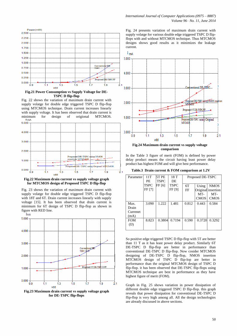
Fig. 22 shows the variation of maximum drain current with
supply volatge for double edge triggered TSPC D flip-flop
using MTCMOS technique. Drain current increases linearly
with supply voltage. It has been observed that drain current is
minimum for design of origional MTCMOS.
Fig.22 Maximum drain current vs supply voltage graph
for MTCMOS design of Proposed TSPC D flip-flop
Fig. 23 shows the variation of maximum drain current with
supply volatge for double edge triggered TSPC D flip-flop
with 18T and 6T. Drain current increases linearly with supply
voltage [15]. It has been observed that drain current is
minimum for 6T design of TSPC D flip-flop as shown in
figure with RED line.
Fig.23 Maximum drain current vs supply voltage graph
for DE-TSPC flip-flops
Fig. 24 presents variation of maximum drain current with
supply volatge for various double edge triggered TSPC D flip-
flops with and without MTCMOS technique. Thus MTCMOS
designs shows good results as it minimizes the leakage
current.
Fig.24 Maximum drain current vs supply voltage
comparison
In the Table 3 figure of merit (FOM) is defined by power
delay product means the circuit having least power delay
product has highest FOM and will give best performance.
Table.3 Drain current & FOM comparison at 1.2V
Parameter 11T
PE
TSPC
FF [7]
5T PE
TSPC
FF [6]
18 T
DE
TSPC
FF [9]
Proposed DE-TSPC
6T
FF
Using
Original
MT-
CMOS
NMOS
insertion
MT-
CMOS
Max.
Drain
Currenet
(mA)
3.090 1.222 1.481 0.812 0.443 0.584
FOM
(fJ)
8.823 0.3804 0.7194 0.590 0.3720 0.3292
So positive edge triggered TSPC D flip-flop with 5T are better
than 11 T as it has least power delay product. Similarly 6T
DE-TSPC D flip-flop are better in performance than
conventional DE-TSPC D flip-flop. Now cosider MTCMOS
designing of DE-TSPC D flip-flop, NMOS insertion
MTCMOS design of TSPC D flip-lop are better in
performance than the original MTCMOS design of TSPC D
flip-flop. it has been observed that DE-TSPC flip-flops using
MTCMOS technique are best in performance as they have
highest figure of merit (FOM).
Graph in Fig. 25 shows variation in power dissipation of
different double edge triggered TSPC D flip-flop. this graph
reveals that power dissipation for conventional DE-TSPC D
flip-flop is very high among all. All the design technologies
are already discussed in above sections.

International Journal of Computer Applications (0975 – 8887)
Volume 96– No. 11, June 2014
51
Fig. 25 Power dissipation for different DE-TSPC D FF
7. CONCLUSION The true single-phase clock (TSPC) type is a common
dynamic flip-flop variety which performs the flip-flop
operation with low power and at high speeds. However,
dynamic flip-flops will typically not work at low clock
speeds, required enough time, leakage paths may discharge
the parasitic capacitance enough to cause the flip-flop to enter
invalid states. An efficient design of double edge triggered
True Single Phase Clocking (TSPC) D flip-flop is presented.
The main advantage of TSPC dynamic CMOS circuit is that it
is small in area, no clock skew and can achieve the higher
clock rates. Hence it is a promising storage element in low
power VLSI designs. The originally developed TSPC flip-flop
are very sensitive to the clock slope and large portion of
power is spent in pre-charging the internal nodes, which
makes TSPC dynamic circuits less power efficient. In the
conventional CMOS design, high leakage current is becoming
a significant contributor to power dissipation. To overcome
the existing problem of CMOS TSPC D flip-flop, a Multi-
threshold CMOS (MTCMOS) technology is used for leakage
minimization. The proposed schematic design of DE-TSPC D
flip-flop is based on MTCMOS technique. The basic concept
in the designing is using transistors with different threshold
voltages (Vth). The MTCMOS design of TSPC flip -flop is
having least power delay product (PDP) thus highest figure
of merit hence it gives best performance and it can be used in
several applications like level converters, microprocessors,
clocking system counter etc. It is recorded that proposed
original MTCMOS implmentation and NMOS insertion in
MTCMOS design of TSPC D flip-flop saves static power
57.517% and 58.871% as compared to conventional DE-
TSPC D flip-flop respectively at 1.2V. Further these designs
are compared with 6T TSPC D flip-flop and improvement is
obtained in terms power consumption as they saves 50.23%
and 51.82% respectively at 1.2V. Proposed DE-TSPC flop-
flop shows good performance with supply voltage vs drain
current variations as compare to conventional DE-TSPC flip-
flop.
8. REFERENCE [1] S. Unger and C. Tang, "Clocking Schemes for Very
High-Speed Digital Systems”, IEEE Transaction on
Computers, Vol.: C-35, pp. 880-895, October 1986.
[2] M. Pedram, “Power minimization in IC Design: Principles
and applications,” ACM Transactions on Design
Automation of Electronic Systems, Vol. 1, pp. 3-56,
January 1996.
[3] B. Nikolic, “Design in The Power Limited Scaling
Regime,” IEEE Transaction on Electronic Devices, Vol.
55, No. 1, pp. 71-83, January 2008.
[4] Neil H. E. Weste, David Harris, Ayan Banerjee, CMOS
VLSI DESIGN: A Circuits and Systems Prespective,
Third Edition, pp. 129-131, 2009.
[5] S. Tahmasbi Oskuii, A. Alvandpour, “Comparative Study
on Low-Power High- Performance Standard- Cell Flip-
Flops”, Microelectronics: Design, Technology, and
Packaging, in Proceedings of the International Society
for Optics and Photonics (SPIE), Vol. 5274, pp. 390-398,
2004.
[6] Surya Naik and Rajeevan Chandel, “Design of a Low
Power Flip-Flop Using CMOS Deep Submicron
Technology”, IEEE, International Conference on Recent
Trends in Information, Telecommunication and
Computing (ITC), pp. 253-256, 2010.
[7] Neil H. E. Weste, David Harris, Ayan Banerjee, a book
on “CMOS VLSI Design a Circuits and Systems
Perspective”, Pearson Education, 3rd Edition, pp. 275-
275, 2009.
[8] J. A. Butts and G.S. Sohi, “A Static Power Model for
Architects”, IEEE, In Proceedings of the 33rd Annual
International Symposium on Micro-architecture, pp. 191-
201, 2000.
[9] J. S. Wang, “A New True-Single-Phase-Clocked Double
Edge Triggered Flip-Flop for Low-Power VLSI Design”,
in Proceedings of IEEE International Symposium on
Circuit and Systems, pp. 1896-1899, 12 June 1997.
[10] M Afghahi and C. Svenson, “A Unified Single Phase
Clocking Scheme for VLSI Systems”, IEEE Journal
Solid-State and Circuits, Vol. 25, pp. 255-233, February
1990.
[11] B. Pontikakis and M. Nekhili. “A New Area Efficient
Split- Output TSPC CMOS Latch for High Speed VLSI
Applications”, IEEE, International Conference of
Microelectronics (ICM), pp. 101-104, 2002.
[12] L. Wei, Z. Chen, M. Johnson, K. Roy and V. De,
“Design and Optimization of Low Voltage High
Performance Dual Threshold CMOS Circuits,” IEEE
Transactions on Very Large Scale Integration (VLSI)
Systems, pp. 16 – 24, March 1999.
[13] S. Mutoh et al., “A 1V Multi-Threshold Voltage CMOS
DSP with an Efficient Power Management Technique for
Mobile Phone Application”, IEEE Journal of Solid-State
Circuits, Vol. 31, No.11, pp. 1795–1802, 1996.
[14] Etienne Sicard, Sonia Ben Dhia, Syed Mahfuzul Aziz,
“Teaching CMOS Circuit Desig in Nano-scale
Technologies Using MICROWIND”, Proceedings of
the European workshop on microelectronics education,
pp. 78-83, May 2010.
[15] Jayanth Srinivasan, “An Overview of Static Power
Dissipation”, CiteSeer public search engine and digital
libraries for scientific and academic papers in the fields
of computer and information science, pp. 1-7, 30 August
2011.
IJCATM : www.ijcaonline.org


![Statistica descrittiva con R - Laboratorio di Statistica ... · voti_sorted >=75 #vettore di TRUE e FALSE ## [1] TRUE TRUE TRUE TRUE TRUE TRUE TRUE TRUE TRUE TRUE TRUE ## [12]](https://img.pdfslide.net/doc/110x75/5fa7220773f533798518ec4c/statistica-descrittiva-con-r-laboratorio-di-statistica-votisorted-75.jpg)