Embed Size (px)
Citation preview
Truly achromatic optical metasurfaces: a filtercircuit theory-based designJIERONG CHENG AND HOSSEIN MOSALLAEI*Department of Electrical and Computer Engineering, Northeastern University, 360 Huntington Ave., Boston, Massachusetts 02115, USA*Corresponding author: [email protected]
Received 13 July 2015; revised 19 August 2015; accepted 22 August 2015; posted 24 August 2015 (Doc. ID 245732); published 14 September 2015
We propose truly achromatic metasurfaces at midinfrared and visible spectra using plasmonic and all-dielectricconcepts, respectively. The constituting layered elements, with each layer being a capacitive or an inductive struc-ture, behave like low-pass circuit filters with almost linear phase response over the designed spectrum. This allowssuccessful broadband operation. The plasmonic layered elements are limited to work around 50 THz due to theappearance of a plasmonic resonance feature at higher frequencies. On the other hand, the all-dielectric conceptcan be designed up to the visible range with negligible material dispersion. Design procedures and working prin-ciples are fully detailed. Two types of metasurfaces patterned by plasmonic and all-dielectric elements are carefullydesigned and numerically simulated around 50 and 600 THz, respectively. Chromatic aberration is successfullyavoided. The plasmonic metasurface operates well in 5.5–7.5 μm, and the all-dielectric case has the desired per-formance over almost the entire visible band. © 2015 Optical Society of America
OCIS codes: (160.3918) Metamaterials; (050.5080) Phase shift; (260.2030) Dispersion.
http://dx.doi.org/10.1364/JOSAB.32.002115
1. INTRODUCTION
Metasurfaces have been of great interest for wavefront engineer-ing by providing a space-variant phase shift from constitutingsubwavelength inclusions [1–3]. Different from the traditionalrealization based on the propagation accumulation, the phaseshift here is generated abruptly within an ultrathin layer due tothe resonant interaction between the incoming light and theinclusions. Such resonance provides large flexibility to reconfig-ure the amplitude, phase, and polarization responses of thescattered light, realized by manipulating the element material,geometry, period, and orientation. A variety of innovative func-tionalities have been demonstrated ranging from microwave tovisible ranges, including anomalous reflection and refraction[4,5], beaming and focusing [6,7], information processing[8,9], vortex beam generation [10], quarter and half-wave plate[11], phase holograms [12], and so forth.
At the same time, it is the resonant nature of the phase shiftthat brings a common limitation for many applications of suchkind of metasurfaces, which is the single-frequency or narrow-band operation (around 5% or even less). Although the band-width can be increased by cascading resonant elements [13,14],the phase profile across the entire surface is frequency-dependent and changes either rapidly or slowly dependingon the quality factor of the element resonance, hamperingwidespread applications.
Achromatic wavefront shaping is highly desirable for numer-ous applications, including communication systems, sensing,
imaging, and energy harvesting. Several techniques have beenproposed to address the issue of narrow bandwidth. One modelis to change the multiband design into broadband design bymerging multiple closely positioned resonances [15,16], wherecomplex element structures are usually needed. Another type ofbroadband metasurfaces can maintain the performance fairlywell within a certain frequency range, although these surfacesare designed to operate at one selected frequency [17,18]. Suchbandwidth is uncontrollable, and the performance is still fre-quency-dependent. For example, the bending angle of theanomalous beam is different because the frequency changesin the V-shaped nanoantennas array [18]. The focal lengthand the spot intensity are varying with frequency in the broad-band flat mirrors [17]. Thus, such wideband operation suffersfrom chromatic aberration.
Geometric metasurfaces made of a single layer of dipole an-tennas have been reported recently for dispersionless wavefrontshaping [19–21]. The phase gradient of the cross polarizationdoes not depend on the dispersion of the dipole antennas butdepends on the orientation of the dipoles when the surface isilluminated by the circularly polarized wave only. The effi-ciency is inherently limited due to the cross-polarization work-ing scheme, though.
Truly broadband operation requires a constant group delayprofile (i.e., a linear phase delay profile) as group delay is therate of phase variation over frequency. Otherwise, changing thefrequency will change the phase response of each element
Research Article Vol. 32, No. 10 / October 2015 / Journal of the Optical Society of America B 2115
0740-3224/15/102115-07$15/0$15.00 © 2015 Optical Society of America
undesirably, and the performance will be degraded. Recently, abroadband true-time-delay microwave lens was theoreticallyand experimentally demonstrated based on the filter circuittheory. It is composed of subwavelength unit cells of closelyspaced capacitive and inductive layers [22,23]. Each layer of theunit cell is a nonresonant structure, and the proper cascading ofthe layers in the propagation direction forms a spatial filter witha designed bandpass or low-pass response. Within the operationband, the phase response is linear and the group delay is con-stant, enabling the truly dispersionless broadband operation.
In this work, we theoretically extend this mechanism frommicrowave to infrared and visible ranges. Material dispersion ofthe metallic layers prohibits us to directly scale up the micro-wave design, and a comprehensive design study must be per-formed. Also, the plasmonic effect poses limitations that suchbroadband metasurface can work only up to the midinfraredrange. The metallic patches and wires begin to resonate athigher frequencies, and they cannot be treated as purecapacitors or inductors. We also investigate the concept of all-dielectric metasurfaces made of high/low-index dielectriclayered unit cells functioning at the visible frequency range.
Specifically, the design principle of the broadband phaseshift element is generally stated based on the filter circuittheory. Then, such element is realized, respectively, by layeredplasmonic patches separated by dielectric spacers at themidinfrared range and by all-dielectric layers with alternatinghigh and low refractive indices at the visible range. Twotypes of metasurface lenses without chromatic aberration aredesigned and numerically demonstrated at 40 to 55 THz(∼5.5–7.5 μm) and 450 to 750 THz (covering almost theentire visible band) using plasmonic and all-dielectric layeredconcepts, respectively. To the best of our knowledge, these willbe the first truly wideband metasurfaces designed at a high-frequency range. Also, wideband beam scanning performanceis demonstrated due to the deep subwavelength thickness andthe element period.
2. PHASE MANIPULATION BASED ON FILTERTHEORY
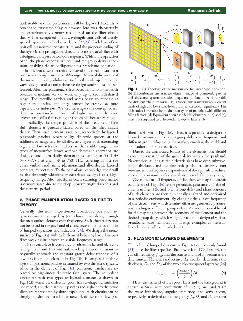
Generally, the truly dispersionless broadband operation re-quires a constant group delay (i.e., a linear phase delay) throughthe metasurface element over frequency. Such characterizationcan be found in the passband of a microwave filter circuit madeof lumped capacitors and inductors [24]. We design the meta-surface of Fig. 1(a) with each element behaving like a low-passfilter working in infrared to visible frequency ranges.
The metasurface is composed of ultrathin layered elementsin Figs. 1(b) and 1(c) with subwavelength lattice constant tophysically approach the constant group delay response of alow-pass filter. The element in Fig. 1(b) is composed of threelayers of plasmonic patches separated by two dielectric spacers,while in the element of Fig. 1(c), plasmonic patches are re-placed by high-index dielectric thin layers. The equivalentcircuit for such two types of layered elements is shown inFig. 1(d), where the dielectric spacer has a π-shape transmissionline model, and the plasmonic patches and high-index dielectricslices are represented by shunt capacitors. Such circuits can besimply transformed to a ladder network of five-order low-pass
filters, as shown in Fig. 1(e). Thus, it is possible to design thelayered elements with constant group delay over frequency anddifferent group delay along the surface, enabling the widebandapplication of the metasurface.
Due to the distributed feature of the elements, one shouldexpect the variation of the group delay within the passband.Nevertheless, as long as the dielectric slabs have deep-subwave-length thickness, and the plasmonic patches are far away fromresonances, the frequency dependence of the equivalent induct-ance and capacitance is fairly weak over a wide frequency range.
Given the cut-off frequency of the filter, we map the circuitparameters of Fig. 1(e) to the geometric parameters of the el-ements in Figs. 1(b) and 1(c). Group delay and phase responseof such elements are then numerically analyzed and optimizedin a periodic environment. By changing the cut-off frequencyof the circuit, one will determine different geometric parame-ters, leading to different group delays. A data set is establishedfor the mapping between the geometry of the element and thedesired group delay, which will guide us in the design of variousbroadband wave manipulation. Design examples of metasur-face elements will be detailed next.
3. PLASMONIC LAYERED ELEMENTS
The values of lumped elements in Fig. 1(e) can be easily found[25] once the filter type (i.e., Butterworth and Chebyshev), thecut-off frequency f cut, and the source and load impedances aredetermined. The series inductance, L1 and L2, determines thethickness, D2 andD4, of the two dielectric spacer layers by [26]
D2;4 � a sin
�ω0L1;2
η
�∕β: (1)
Here, the material of the spacer layer and the background ischosen as SiO2 with permittivity of 2.25. η, ω0, and β arethe wave impedance, angular frequency, and wave vector,respectively, at desired center frequency f 0. D2 andD4 are then
Fig. 1. (a) Topology of the metasurface for broadband operation.(b) Dispersionless metasurface element made of plasmonic patchesand dielectric spacers cascaded sequentially. Patch size is variablefor different phase responses. (c) Dispersionless metasurface elementmade of high and low index dielectric layers cascaded sequentially. Thehigh index is variable by mixing two types of materials with differentfilling factors. (d) Equivalent circuit model for elements in (b) and (c),which is simplified as a five-order low-pass filter in (e).
2116 Vol. 32, No. 10 / October 2015 / Journal of the Optical Society of America B Research Article

fixed for different group delay elements to keep the uniformthickness over the surface. C11 and C22 are known basedon these slab thicknesses. Values for C 0
1, C02, and C 0
3 can bederived accordingly. Given a deep-subwavelength period Λ,C 0
1, C02, and C 0
3 can be converted to plasmonic patch sizeS1, S3, and S5, with ultrathin thickness D1, D3, and D5, whichis detailed as follows.
When the period Λ is much smaller than the wavelength,and the metallic patches are perfect electrical conductors(PEC), which is the case at microwave frequency, they act aspure capacitors between the adjacent patch edges for theorthogonally incoming light. The relation between the capaci-tance and the geometrical size of the patch can be found in[27]. As the frequency increases, the permittivity of metalshould be described by the Drude model, and the finite thick-ness, even though in the deep subwavelength scale, also plays arole in the optical response. Thus, the mapping between thecapacitance and the geometrical parameters should be modi-fied. Here, finite-difference time-domain (FDTD) simulationsare used to capture the effective capacitance of the periodicmetallic patches with different patch size S.
The plasmonic patch is made of Au with the permittivitymodeled by the Drude model [28]. It is periodically patternedwithin the x–y plane and embedded in the uniform backgroundwith relative permittivity of 2.25. To obtain the equivalentcapacitance, the transmission and reflection spectrums of peri-odic patches with desired patch size are numerically obtained inFDTD with plane wave excitation propagating along z and po-larized along x. Then, the theoretical transmission and reflec-tion of a pure capacitor are calculated from the circuit theoryand fitted to the numerical results to obtain the optimumequivalent capacitance. Figure 2(a) shows a specific exampleworking around 50 THz. The period of the patch is λ0∕6,where λ0 is the free-space wavelength at 50 THz. The patchsize is 480 nm with the thickness of λ0∕150. The numericalresponses (solid lines) and the theoretical results (dots) agreeperfectly within a large bandwidth centered at 50 THz, whenthe equivalent capacitance for such periodic patch is givenas C � 3.71 aF.
To further detect the upper-frequency limit when the Aupatch behaves as a capacitor, we then move the working fre-quency to the near-infrared range around 200 THz. The periodis still kept as λ0∕6 and the thickness to be λ0∕25, with λ0 beingthe wavelength at 200 THz. The patch size is scaled accordinglyto 120 nm. The numerical transmission and reflection spec-trums are given as the blue solid lines in Fig. 2(b). The opti-mized fitting results of the green dot lines show large deviationby considering the patch as a pure capacitor. On the otherhand, the response of a capacitor and an inductor in series givessatisfactory agreement with the numerical results as the red dot-ted lines, when C � 0.83 aF and L � 0.351 pH. This meansthat the patch itself is a plasmonic resonant structure around200 THz and cannot be modeled by a pure capacitor. Thus, welimit the dispersionless plasmonic element design to the mid-infrared range around 50 THz.
Figure 3 shows the relation between the capacitance andthe patch size using the same period and patch thickness inFig. 2(a) from 30 to 70 THz. The mapping relation for patchesmade of PEC is also given as a comparison. As can be seen, toachieve the same capacitance, the required patch size is smallerfor the Au patch compared with the PEC patch, which meansone cannot directly scale the microwave design up to the mid-infrared range. The plasmonic patch should be shrunkenappropriately to achieve good performance.
Next, the dispersionless elements are designed for differentgroup delays. The element is made to mimic the five-orderChebyshev 0.1 dB low-pass filter. The relative permittivityof the background and the dielectric layers is 2.25. The dielec-tric layer thickness, D2 and D4, is calculated to be 540 nmwhen f cut � 90 THz and f 0 � 50 THz. Then, four differentperiodic elements are shown with cut-off frequency off cut � ∞, 80, 60, and 45 THz. C 0
1, C02, and C 0
3 are derivedfor each case, and the patch sizes S1, S3, and S5 are determinedbased on Fig. 3. The total thickness of the five-layer element is1.2 μm with a transverse period of 1 μm. The transmissionamplitude, phase, and group delay of each periodic elementare detailed in Fig. 4. It is worth noting that the realizedcut-off frequencies for the elements are different from thedesigned ones. This is due to the fixed dielectric layer thickness,which cannot provide the ideal inductance for all the filter
Fig. 2. (a) Transmission and reflection spectrums of periodicAu patches around 50 THz with period of 1 μm, patch size of480 nm, and thickness of 40 nm. Solid blue lines: FDTD numericalresults; green dots: theoretical fitting using a pure capacitor withC � 3.71 aF. (b) Transmission and reflection spectrums around200 THz of periodic Au patches with period of 250 nm, patch sizeof 120 nm, and thickness of 10 nm. Solid blue lines: FDTD numericalresults; green dotted line: theoretical fitting using a pure capacitor withC � 1.86 aF; red dotted lines: theoretical fitting using series capacitorand inductor with C � 0.83 aF and L � 0.351 pH.
Fig. 3. Correlation between the plasmonic patch size and thecapacitance. Blue solid line: capacitance of 40 nm thick periodicAu patch with period of 1 μm obtained numerically around 50 THz,where the permittivity is a Drude model. Red dashed line: theoreticalcapacitance of PEC patch with the same period. At midinfrared range,in order to obtain the same capacitance, one should use smaller Aupatch size compared with the PEC.
Research Article Vol. 32, No. 10 / October 2015 / Journal of the Optical Society of America B 2117

responses. Nevertheless, within the shaded frequency range [4055] THz, group delays can still be viewed as constant approx-imately for all the elements. Linear phase response and hightransmission efficiency are achieved at the same time.
The maximum group delay variation among the elements inFig. 4(c) is 7.3 fs within the [40 55] THz band. The smallestgroup delay is the case when all the plasmonic patches are ab-sent, corresponding to the cut-off frequency of ∞. As the cut-off frequency moves close to 50 THz, the group delay valueincreases. Meanwhile, the variation of the group delay increasesdue to the deviation from the ideal filter components. Thus,there is a trade-off relation between the available group delayrange and the operation bandwidth. One way to further in-crease the group delay range without sacrificing the bandwidthis to use higher-order filter elements with more layers, whichwill increase the fabrication complexity.
4. ALL-DIELECTRIC LAYERED ELEMENTS
Plasmonic layered elements are limited to work at the midin-frared range due to the resonant nature of the patches at higherfrequencies. To overcome such limitation, the patch can be
replaced by an ultrathin layer of high-index dielectric slab.The equivalent circuit for such a slab is simplified into a shuntcapacitor. Thus, the all-dielectric layered element in Fig. 1(c) ismade of five layers of dielectric slabs, with the second and thefourth layers to be the low-index SiO2 slabs to provide the seriesinductors, and the remaining three high-index layers to providethe parallel capacitors like the plasmonic patches. At the mid-infrared range, plasmonic patch size is a tunable parameter torealize different group delays. Here, the equivalent index of theslab can be changed by mixing two types of dielectrics for therealization of different group delays. We mix Si (relative per-mittivity of 12.25) and SiO2 within a subwavelength period toobtain different indices and different capacitances for the first,third, and fifth layers. The thickness of each slab layer is stillfixed considering the feasibility of fabrication.
The design principle of such element is the same as the plas-monic case, except that the mapping relation is from C 0
1, C02,
and C 03 to the equivalent indices and finally to the filling factors
of SiO2 in Si slab for the first, third, and fifth layers. Next, asample element is designed to work around 500 THz with cut-off frequency of 800 THz. The second and fourth layers areSiO2 slabs with thickness of 18 nm. The thickness of thehigh-index layer can be arbitrarily small theoretically. But unre-alistically high index is needed if the slab is too thin.Considering the largest available permittivity of 12.25, thethickness of the first, third, and fifth layers is given asD1 � 15 nm, D3 � 25 nm, and D5 � 15 nm, respectively.Thus, the total thickness of such element is 91 nm. The relativepermittivity of each layer (ε1;3;5) is related to the desired capaci-tance (C 0
1, C02, C
03) by the following equation:
−jη0ffiffiffiffiffiffiffiffiffiε1;3;5
p cot� ffiffiffiffiffiffiffiffiffi
ε1;3;5p
β0D1;3;5
�� 1
jω0C 01;2;3
; (2)
where β0 and η0 are for the free-space case at the center fre-quency ω0. The required relative permittivity for each layerin this element is calculated to be 6.32, 6.47, and 6.32.The mixing ratio of SiO2 and Si to realize the permittivityin each layer can be determined by the effective medium theory(EMT) [28] if the period is in subwavelength scale.
One should note that the choice of the period can be arbi-trarily small and will be limited by the fabrication ability. Eachlayer is a nonresonant structure. The interaction of the cascad-ing layers provides the desired response, which does not dependon the period. Here, we use the period of Λ � 50 nm (λ0∕12at 500 THz) in order to ensure that EMT works perfectly todetermine the indices of the first, third, and fifth layers. Thefilling factor of the SiO2 inside the Si slab is defined as S∕Λ,where S is the side length of the SiO2 square, as shown inFig. 1(c). The effective permittivity of the designed slabfollows [29]
ffiffiffiffiffiffiεeff
p ��1 −
S2
Λ2
� ffiffiffiffiffiεSi
p � S2
Λ2
ffiffiffiffiffiffiffiffiffiεSiO2
p : (3)
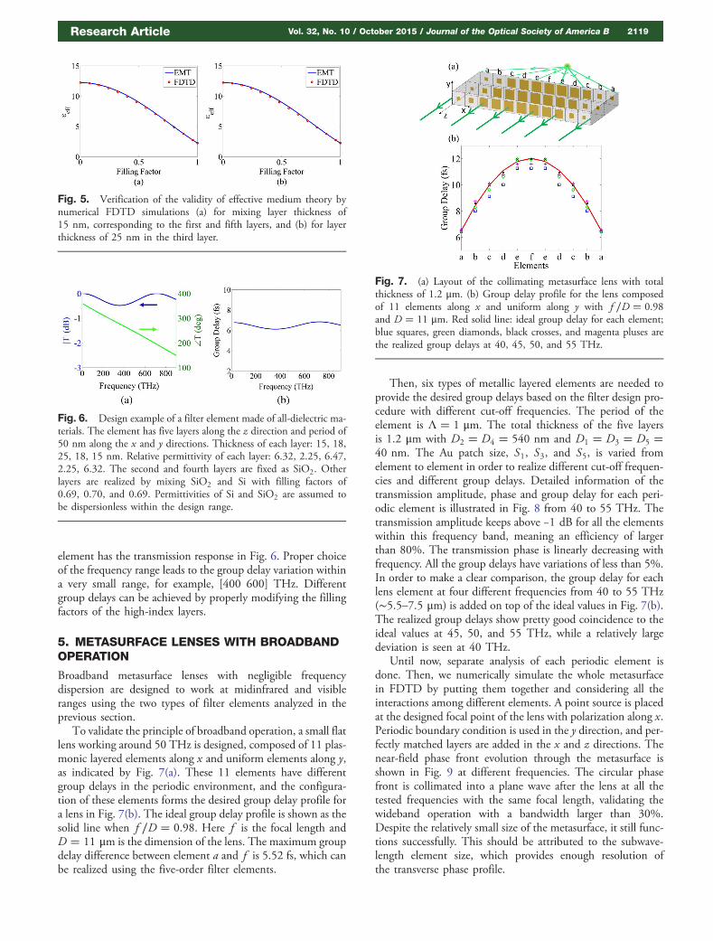
This is verified by the FDTD simulations for the first andfifth layers in Fig. 5(a) and for the third layer in Fig. 5(b), show-ing that the effective permittivity does not depend on the thick-ness of the slab.
Then, the filling factors of SiO2 in the first, third, and fifthlayers are obtained as 0.69, 0.70, and 0.69 to realize the per-mittivities of 6.32, 6.47, and 6.32. Finally, this five-layer
Fig. 4. (a) Transmission amplitudes, (b) phases, and (c) group de-lays of plasmonic elements with designed cut-off frequencies of∞, 80,60, and 45 THz (blue solid line, green diamond line, black cross line,and red circle line, respectively), realized by choosing different patchsizes of S1, S3, and S5. Within the shaded frequency range [4055] THz, all the elements can be viewed as dispersionless.
2118 Vol. 32, No. 10 / October 2015 / Journal of the Optical Society of America B Research Article
element has the transmission response in Fig. 6. Proper choiceof the frequency range leads to the group delay variation withina very small range, for example, [400 600] THz. Differentgroup delays can be achieved by properly modifying the fillingfactors of the high-index layers.
5. METASURFACE LENSES WITH BROADBANDOPERATION
Broadband metasurface lenses with negligible frequencydispersion are designed to work at midinfrared and visibleranges using the two types of filter elements analyzed in theprevious section.
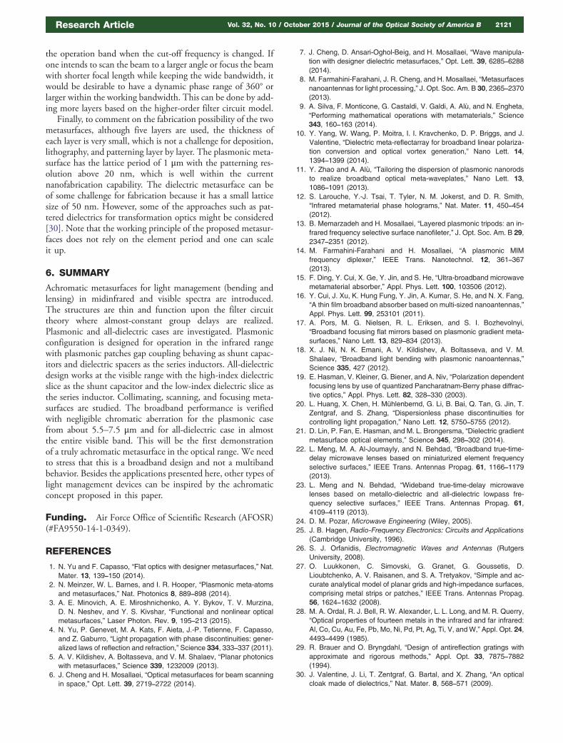
To validate the principle of broadband operation, a small flatlens working around 50 THz is designed, composed of 11 plas-monic layered elements along x and uniform elements along y,as indicated by Fig. 7(a). These 11 elements have differentgroup delays in the periodic environment, and the configura-tion of these elements forms the desired group delay profile fora lens in Fig. 7(b). The ideal group delay profile is shown as thesolid line when f ∕D � 0.98. Here f is the focal length andD � 11 μm is the dimension of the lens. The maximum groupdelay difference between element a and f is 5.52 fs, which canbe realized using the five-order filter elements.
Then, six types of metallic layered elements are needed toprovide the desired group delays based on the filter design pro-cedure with different cut-off frequencies. The period of theelement is Λ � 1 μm. The total thickness of the five layersis 1.2 μm with D2 � D4 � 540 nm and D1 � D3 � D5 �40 nm. The Au patch size, S1, S3, and S5, is varied fromelement to element in order to realize different cut-off frequen-cies and different group delays. Detailed information of thetransmission amplitude, phase and group delay for each peri-odic element is illustrated in Fig. 8 from 40 to 55 THz. Thetransmission amplitude keeps above −1 dB for all the elementswithin this frequency band, meaning an efficiency of largerthan 80%. The transmission phase is linearly decreasing withfrequency. All the group delays have variations of less than 5%.In order to make a clear comparison, the group delay for eachlens element at four different frequencies from 40 to 55 THz(∼5.5–7.5 μm) is added on top of the ideal values in Fig. 7(b).The realized group delays show pretty good coincidence to theideal values at 45, 50, and 55 THz, while a relatively largedeviation is seen at 40 THz.
Until now, separate analysis of each periodic element isdone. Then, we numerically simulate the whole metasurfacein FDTD by putting them together and considering all theinteractions among different elements. A point source is placedat the designed focal point of the lens with polarization along x.Periodic boundary condition is used in the y direction, and per-fectly matched layers are added in the x and z directions. Thenear-field phase front evolution through the metasurface isshown in Fig. 9 at different frequencies. The circular phasefront is collimated into a plane wave after the lens at all thetested frequencies with the same focal length, validating thewideband operation with a bandwidth larger than 30%.Despite the relatively small size of the metasurface, it still func-tions successfully. This should be attributed to the subwave-length element size, which provides enough resolution ofthe transverse phase profile.
Fig. 5. Verification of the validity of effective medium theory bynumerical FDTD simulations (a) for mixing layer thickness of15 nm, corresponding to the first and fifth layers, and (b) for layerthickness of 25 nm in the third layer.
Fig. 6. Design example of a filter element made of all-dielectric ma-terials. The element has five layers along the z direction and period of50 nm along the x and y directions. Thickness of each layer: 15, 18,25, 18, 15 nm. Relative permittivity of each layer: 6.32, 2.25, 6.47,2.25, 6.32. The second and fourth layers are fixed as SiO2. Otherlayers are realized by mixing SiO2 and Si with filling factors of0.69, 0.70, and 0.69. Permittivities of Si and SiO2 are assumed tobe dispersionless within the design range.
Fig. 7. (a) Layout of the collimating metasurface lens with totalthickness of 1.2 μm. (b) Group delay profile for the lens composedof 11 elements along x and uniform along y with f ∕D � 0.98and D � 11 μm. Red solid line: ideal group delay for each element;blue squares, green diamonds, black crosses, and magenta pluses arethe realized group delays at 40, 45, 50, and 55 THz.
Research Article Vol. 32, No. 10 / October 2015 / Journal of the Optical Society of America B 2119

Although the periodic elements are analyzed under normalexcitation, their wideband performance is kept well for theoblique incidence in Fig. 10. The subwavelength element sizeand small thickness make the whole lens not sensitive to theincident angle. To further utilize this advantage, the collima-tion direction can be scanned by moving the excitation sourcealong the focal plane, as shown in Fig. 10. The point source isnow located at x � 3 μm along the focal plane. The time
delays after the 11 lens elements are not uniform but decreasinglinearly from the −x to �x direction, thus leading to a scannedcollimation beam. The time delay difference between adjacentelements after the lens is calculated to be 1.25 fs, which cor-responds to the bending angle of 15.5°. And the simulated re-sults are consistent with the expectation over the designedbandwidth. By moving the source further away from the centeralong x, the beam can be scanned to a wider angular range.
To realize achromatic operation at the visible range, a focus-ing metasurface lens made of all-dielectric layered elements isdesigned and analyzed numerically. The layout is in the x–yplane with 19 elements along the x and periodic along the ydirection. The elements have the same parameters as the exam-ple in Fig. 6, except for the fractions of SiO2 in the Si layers. Bytuning the filling fractions in the first, third, and fifth layers ofthe element, they provide the desired group delay profile for alens with f ∕D � 1 and D � 0.95 μm. The total thickness ofthis metasurface is 91 nm, which is less than λ0∕5 consideringthe center frequency of 600 THz. The uniform plane wave islaunched into this metasurface along the z direction with theelectric field polarized along x. The focusing phenomenon isnumerically analyzed in Fig. 11 from 450 to 750 THz with50 THz steps. Intensity of the electric field is plotted after nor-malization. The focal point is marked in each frequency case.The focal length does not change much across the whole visiblerange. Thus, the chromatic aberration is successfully mini-mized. In addition, because we are modeling a finite size meta-surface, obviously the larger the frequency, the narrower thespot size, as the electrical size of the structure is larger at a higherfrequency.
For either the plasmonic or the all-dielectric elementsdesigned here, the available phase range is limited within
Fig. 8. (a) Transmission amplitudes, (b) phases, and (c) group de-lays over frequency for all the lens elements from a to f in a periodicenvironment. Elements e and f are the same here due to the tiny dif-ference between them. Blue squares: element a; green diamonds:element b; black crosses: element c; red pluses: element d ; magentacircles: elements e and f .
Fig. 9. Phase front evolution of a point source before and after themetasurface composed of plasmonic elements, showing the samecollimation performance from 40 to 55 THz. Dashed lines are thecross section of the plasmonic patches.
Fig. 10. Collimation direction is scanned to 15° by moving thepoint source to x � 3 μm along the focal plane from 40 to 55 THzusing the plasmonic metasurface.
Fig. 11. Beam focusing through the all-dielectric layered metasur-face from 450 to 750 THz with 50 THz steps. The transverse dimen-sion along x is 0.95 μm, and the total thickness is 91 nm. The focalpoint is marked by a black plus sign in each frequency, which showsextremely minor chromatic aberration.
2120 Vol. 32, No. 10 / October 2015 / Journal of the Optical Society of America B Research Article
the operation band when the cut-off frequency is changed. Ifone intends to scan the beam to a larger angle or focus the beamwith shorter focal length while keeping the wide bandwidth, itwould be desirable to have a dynamic phase range of 360° orlarger within the working bandwidth. This can be done by add-ing more layers based on the higher-order filter circuit model.
Finally, to comment on the fabrication possibility of the twometasurfaces, although five layers are used, the thickness ofeach layer is very small, which is not a challenge for deposition,lithography, and patterning layer by layer. The plasmonic meta-surface has the lattice period of 1 μm with the patterning res-olution above 20 nm, which is well within the currentnanofabrication capability. The dielectric metasurface can beof some challenge for fabrication because it has a small latticesize of 50 nm. However, some of the approaches such as pat-tered dielectrics for transformation optics might be considered[30]. Note that the working principle of the proposed metasur-faces does not rely on the element period and one can scaleit up.
6. SUMMARY
Achromatic metasurfaces for light management (bending andlensing) in midinfrared and visible spectra are introduced.The structures are thin and function upon the filter circuittheory where almost-constant group delays are realized.Plasmonic and all-dielectric cases are investigated. Plasmonicconfiguration is designed for operation in the infrared rangewith plasmonic patches gap coupling behaving as shunt capac-itors and dielectric spacers as the series inductors. All-dielectricdesign works at the visible range with the high-index dielectricslice as the shunt capacitor and the low-index dielectric slice asthe series inductor. Collimating, scanning, and focusing meta-surfaces are studied. The broadband performance is verifiedwith negligible chromatic aberration for the plasmonic casefrom about 5.5–7.5 μm and for all-dielectric case in almostthe entire visible band. This will be the first demonstrationof a truly achromatic metasurface in the optical range. We needto stress that this is a broadband design and not a multibandbehavior. Besides the applications presented here, other types oflight management devices can be inspired by the achromaticconcept proposed in this paper.
Funding. Air Force Office of Scientific Research (AFOSR)(#FA9550-14-1-0349).
REFERENCES
1. N. Yu and F. Capasso, “Flat optics with designer metasurfaces,” Nat.Mater. 13, 139–150 (2014).
2. N. Meinzer, W. L. Barnes, and I. R. Hooper, “Plasmonic meta-atomsand metasurfaces,” Nat. Photonics 8, 889–898 (2014).
3. A. E. Minovich, A. E. Miroshnichenko, A. Y. Bykov, T. V. Murzina,D. N. Neshev, and Y. S. Kivshar, “Functional and nonlinear opticalmetasurfaces,” Laser Photon. Rev. 9, 195–213 (2015).
4. N. Yu, P. Genevet, M. A. Kats, F. Aieta, J.-P. Tetienne, F. Capasso,and Z. Gaburro, “Light propagation with phase discontinuities: gener-alized laws of reflection and refraction,” Science 334, 333–337 (2011).
5. A. V. Kildishev, A. Boltasseva, and V. M. Shalaev, “Planar photonicswith metasurfaces,” Science 339, 1232009 (2013).
6. J. Cheng and H. Mosallaei, “Optical metasurfaces for beam scanningin space,” Opt. Lett. 39, 2719–2722 (2014).
7. J. Cheng, D. Ansari-Oghol-Beig, and H. Mosallaei, “Wave manipula-tion with designer dielectric metasurfaces,” Opt. Lett. 39, 6285–6288(2014).
8. M. Farmahini-Farahani, J. R. Cheng, and H. Mosallaei, “Metasurfacesnanoantennas for light processing,” J. Opt. Soc. Am. B 30, 2365–2370(2013).
9. A. Silva, F. Monticone, G. Castaldi, V. Galdi, A. Alù, and N. Engheta,“Performing mathematical operations with metamaterials,” Science343, 160–163 (2014).
10. Y. Yang, W. Wang, P. Moitra, I. I. Kravchenko, D. P. Briggs, and J.Valentine, “Dielectric meta-reflectarray for broadband linear polariza-tion conversion and optical vortex generation,” Nano Lett. 14,1394–1399 (2014).
11. Y. Zhao and A. Alù, “Tailoring the dispersion of plasmonic nanorodsto realize broadband optical meta-waveplates,” Nano Lett. 13,1086–1091 (2013).
12. S. Larouche, Y.-J. Tsai, T. Tyler, N. M. Jokerst, and D. R. Smith,“Infrared metamaterial phase holograms,” Nat. Mater. 11, 450–454(2012).
13. B. Memarzadeh and H. Mosallaei, “Layered plasmonic tripods: an in-frared frequency selective surface nanofileter,” J. Opt. Soc. Am. B 29,2347–2351 (2012).
14. M. Farmahini-Farahani and H. Mosallaei, “A plasmonic MIMfrequency diplexer,” IEEE Trans. Nanotechnol. 12, 361–367(2013).
15. F. Ding, Y. Cui, X. Ge, Y. Jin, and S. He, “Ultra-broadband microwavemetamaterial absorber,” Appl. Phys. Lett. 100, 103506 (2012).
16. Y. Cui, J. Xu, K. Hung Fung, Y. Jin, A. Kumar, S. He, and N. X. Fang,“A thin film broadband absorber based on multi-sized nanoantennas,”Appl. Phys. Lett. 99, 253101 (2011).
17. A. Pors, M. G. Nielsen, R. L. Eriksen, and S. I. Bozhevolnyi,“Broadband focusing flat mirrors based on plasmonic gradient meta-surfaces,” Nano Lett. 13, 829–834 (2013).
18. X. J. Ni, N. K. Emani, A. V. Kildishev, A. Boltasseva, and V. M.Shalaev, “Broadband light bending with plasmonic nanoantennas,”Science 335, 427 (2012).
19. E. Hasman, V. Kleiner, G. Biener, and A. Niv, “Polarization dependentfocusing lens by use of quantized Pancharatnam-Berry phase diffrac-tive optics,” Appl. Phys. Lett. 82, 328–330 (2003).
20. L. Huang, X. Chen, H. Mühlenbernd, G. Li, B. Bai, Q. Tan, G. Jin, T.Zentgraf, and S. Zhang, “Dispersionless phase discontinuities forcontrolling light propagation,” Nano Lett. 12, 5750–5755 (2012).
21. D. Lin, P. Fan, E. Hasman, and M. L. Brongersma, “Dielectric gradientmetasurface optical elements,” Science 345, 298–302 (2014).
22. L. Meng, M. A. Al-Joumayly, and N. Behdad, “Broadband true-time-delay microwave lenses based on miniaturized element frequencyselective surfaces,” IEEE Trans. Antennas Propag. 61, 1166–1179(2013).
23. L. Meng and N. Behdad, “Wideband true-time-delay microwavelenses based on metallo-dielectric and all-dielectric lowpass fre-quency selective surfaces,” IEEE Trans. Antennas Propag. 61,4109–4119 (2013).
24. D. M. Pozar, Microwave Engineering (Wiley, 2005).25. J. B. Hagen, Radio-Frequency Electronics: Circuits and Applications
(Cambridge University, 1996).26. S. J. Orfanidis, Electromagnetic Waves and Antennas (Rutgers
University, 2008).27. O. Luukkonen, C. Simovski, G. Granet, G. Goussetis, D.
Lioubtchenko, A. V. Raisanen, and S. A. Tretyakov, “Simple and ac-curate analytical model of planar grids and high-impedance surfaces,comprising metal strips or patches,” IEEE Trans. Antennas Propag.56, 1624–1632 (2008).
28. M. A. Ordal, R. J. Bell, R. W. Alexander, L. L. Long, and M. R. Querry,“Optical properties of fourteen metals in the infrared and far infrared:Al, Co, Cu, Au, Fe, Pb, Mo, Ni, Pd, Pt, Ag, Ti, V, andW,” Appl. Opt. 24,4493–4499 (1985).
29. R. Brauer and O. Bryngdahl, “Design of antireflection gratings withapproximate and rigorous methods,” Appl. Opt. 33, 7875–7882(1994).
30. J. Valentine, J. Li, T. Zentgraf, G. Bartal, and X. Zhang, “An opticalcloak made of dielectrics,” Nat. Mater. 8, 568–571 (2009).
Research Article Vol. 32, No. 10 / October 2015 / Journal of the Optical Society of America B 2121