Embed Size (px)
Citation preview
BXTOP45PHardware guide
TURBO PROGRAMMERBXTOP45P
USB, MMC, SIMDEVELOPMENT KIT
HARDWARE GUIDE
This document is part of Turbo Programmer documentation. For Developer Documentation, Applications and Examples,
see http://www.bladox.com/
PRELIMINARY
(C) 2004 BLADOX, s.r.o. Czech Republic, EU
www.bladox.com Rev. 02 - 08/22/04 1/24
BXTOP45PHardware guide
Table of contents1.Overview.............................................................................................................................52.Features..............................................................................................................................53.Block diagram.....................................................................................................................64.Connectors and jumpers.....................................................................................................75.Address map.....................................................................................................................126.ATmega pins.....................................................................................................................137.ISP programming..............................................................................................................158.Bootloader and firmware updating....................................................................................159.Redefining USB device settings.......................................................................................1610.Application examples......................................................................................................1611.Component placement on BXTOP45P...........................................................................1712.Schematics.....................................................................................................................1813.Electrical characteristics.................................................................................................2314.Mechanical drawing........................................................................................................2415.Errata..............................................................................................................................24
www.bladox.com Rev. 02 - 08/22/04 2/24
BXTOP45PHardware guide
FiguresBlock diagram........................................................................................................................6Connectors and jumpers........................................................................................................7Component placement.........................................................................................................17Schematics, section MCU....................................................................................................18Schematics, section TESTIO...............................................................................................19Schematics, section POWER SUPPLY...............................................................................20Schematics, section USB....................................................................................................21Schematics, section PORTS...............................................................................................22
www.bladox.com Rev. 02 - 08/22/04 3/24
BXTOP45PHardware guide
TablesAddress map of I/O ports.....................................................................................................12Address map of memory......................................................................................................12
www.bladox.com Rev. 02 - 08/22/04 4/24
BXTOP45PHardware guide
1.OverviewBLADOX introduces the Turbo Programmer, reference number BXTOP45P, which is aneasy-to-use USB, SIM card and MMC card development kit. It is based on ATMELATmega128L microcontroller and FTDI FT8U245BM USB chip, both well known anddocumented with many application examples available worldwide.
ATmega128L microcontroller operates at speed of 8 MHz generated from crystal. It ispossible to load bootloader at first on the top of its FLASH memory and doing onlyapplication program updates subsequently.
USB interface provides power supply for BXTOP45P. Developer must consider totalcurrent consumption in case of expanding BXTOP45P with additional modules not toexceed maximal 100 mA. Device drivers for FTDI devices are available on webpagewww.ftdichip.com and are available for many operating systems.Configuration serial EEPROM memory is connected to USB chip and holds specificsettings of USB device (BXTOP45P here) important for operating system of hostcomputer. Maximum current consumption, Vendor ID, device ID, Product string etc.should be defined here.
2.Features• Self powered USB device (maximal current from USB bus is 100 mA) with
possibility of using external power supply• ATMEL ATmega128L microcontroller
• 128 kB FLASH, 4 kB SRAM,4 kB EEPROM• Timers, UARTs, SPI, I2C• ISP programming
• USB 1.1 interface (FTDI FT8U245BM based)• SIM card interface (3 Volt SIM card power supply and signal levels)• MMC card interface (esp. for ATMEL Dataflash memory card)• 256 kB extra SRAM memory• External expansion connectors
• One 50 pin MLW50G connector with SPI, I2C, CLK, DATA bus, etc.• Two 10 pin MLW10G connectors with 4 read and 4 write 8 bit data ports• Optional 50 pin SAMTEC MB1-150 connector used for TURBO ADAPTER
• Expanding modules with peripheries like LCD, keyboard, push buttons,communication modules etc.
• Bootloader• Firmware update utility
www.bladox.com Rev. 02 - 08/22/04 5/24
BXTOP45PHardware guide
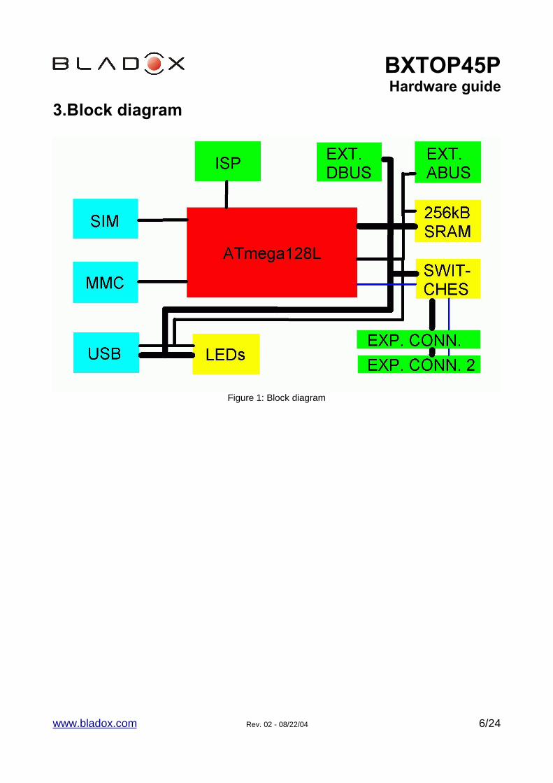
3.Block diagram
www.bladox.com Rev. 02 - 08/22/04 6/24
Figure 1: Block diagram
BXTOP45PHardware guide
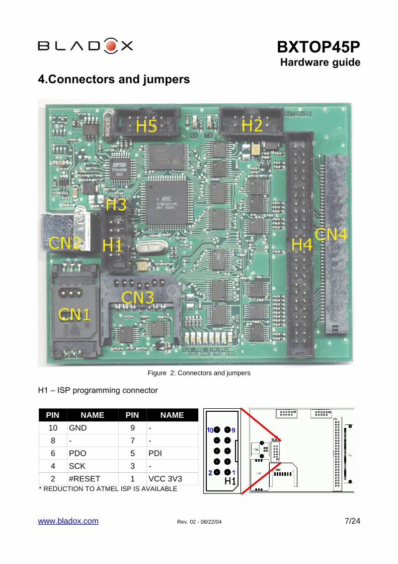
4.Connectors and jumpers
H1 – ISP programming connector
www.bladox.com Rev. 02 - 08/22/04 7/24
Figure 2: Connectors and jumpers
PIN NAME PIN NAME
10 GND 9 -
8 - 7 -
6 PDO 5 PDI
4 SCK 3 -
2 #RESET 1 VCC 3V3* REDUCTION TO ATMEL ISP IS AVAILABLE
BXTOP45PHardware guide
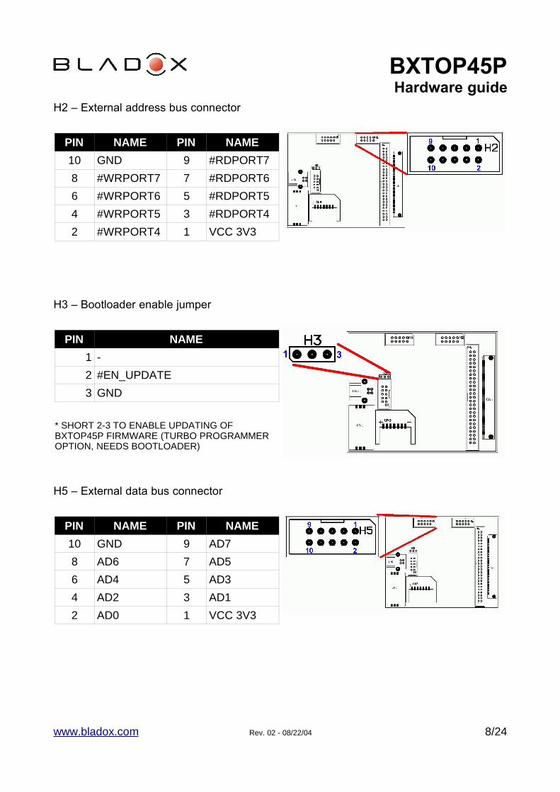
H2 – External address bus connector
H3 – Bootloader enable jumper
H5 – External data bus connector
www.bladox.com Rev. 02 - 08/22/04 8/24
PIN NAME PIN NAME
10 GND 9 #RDPORT7
8 #WRPORT7 7 #RDPORT6
6 #WRPORT6 5 #RDPORT5
4 #WRPORT5 3 #RDPORT4
2 #WRPORT4 1 VCC 3V3
PIN NAME
1 -
2 #EN_UPDATE
3 GND
* SHORT 2-3 TO ENABLE UPDATING OFBXTOP45P FIRMWARE (TURBO PROGRAMMEROPTION, NEEDS BOOTLOADER)
PIN NAME PIN NAME
10 GND 9 AD7
8 AD6 7 AD5
6 AD4 5 AD3
4 AD2 3 AD1
2 AD0 1 VCC 3V3
BXTOP45PHardware guide
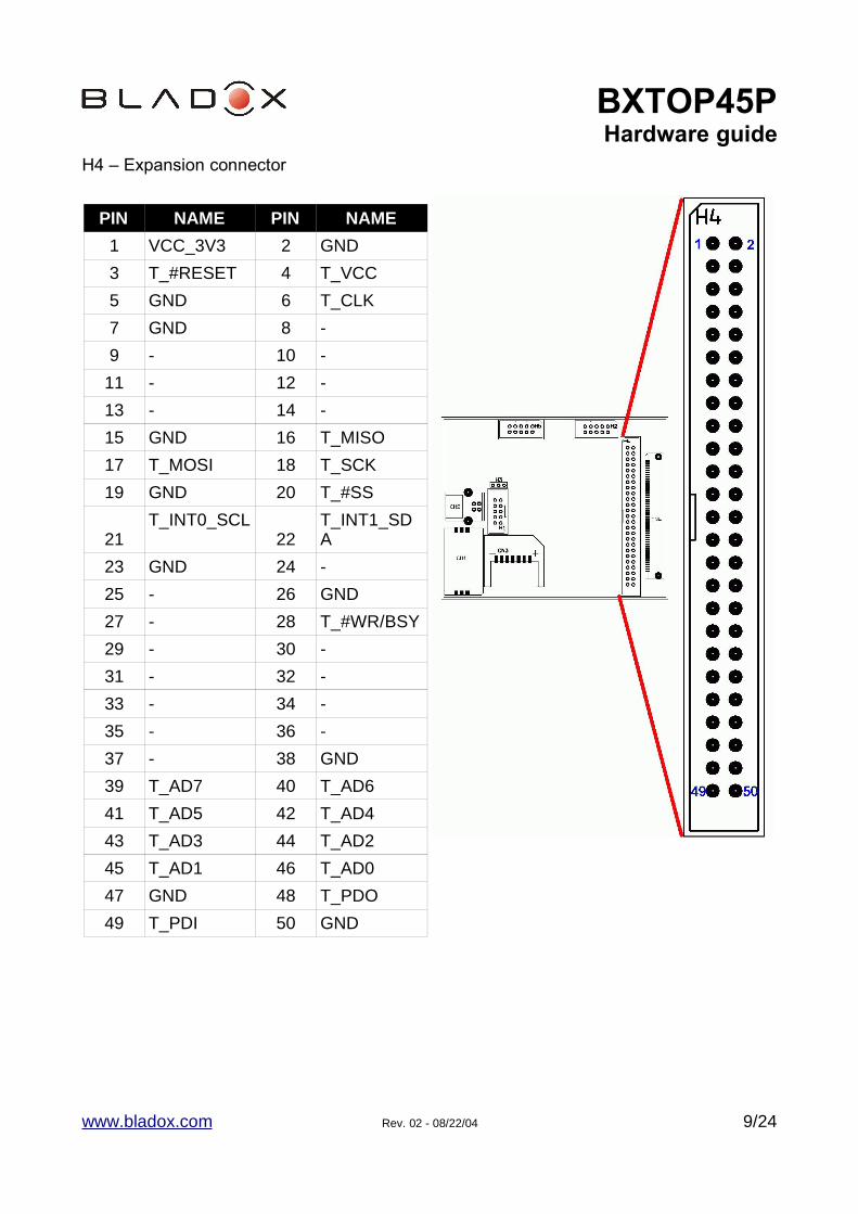
H4 – Expansion connector
www.bladox.com Rev. 02 - 08/22/04 9/24
PIN NAME PIN NAME
1 VCC_3V3 2 GND
3 T_#RESET 4 T_VCC
5 GND 6 T_CLK
7 GND 8 -
9 - 10 -
11 - 12 -
13 - 14 -
15 GND 16 T_MISO
17 T_MOSI 18 T_SCK
19 GND 20 T_#SS
21T_INT0_SCL
22T_INT1_SDA
23 GND 24 -
25 - 26 GND
27 - 28 T_#WR/BSY
29 - 30 -
31 - 32 -
33 - 34 -
35 - 36 -
37 - 38 GND
39 T_AD7 40 T_AD6
41 T_AD5 42 T_AD4
43 T_AD3 44 T_AD2
45 T_AD1 46 T_AD0
47 GND 48 T_PDO
49 T_PDI 50 GND
BXTOP45PHardware guide
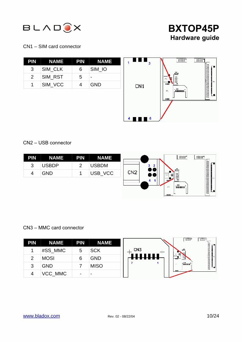
CN1 – SIM card connector
CN2 – USB connector
CN3 – MMC card connector
www.bladox.com Rev. 02 - 08/22/04 10/24
PIN NAME PIN NAME
3 SIM_CLK 6 SIM_IO
2 SIM_RST 5 -
1 SIM_VCC 4 GND
PIN NAME PIN NAME
3 USBDP 2 USBDM
4 GND 1 USB_VCC
PIN NAME PIN NAME
1 #SS_MMC 5 SCK
2 MOSI 6 GND
3 GND 7 MISO
4 VCC_MMC - -
BXTOP45PHardware guide
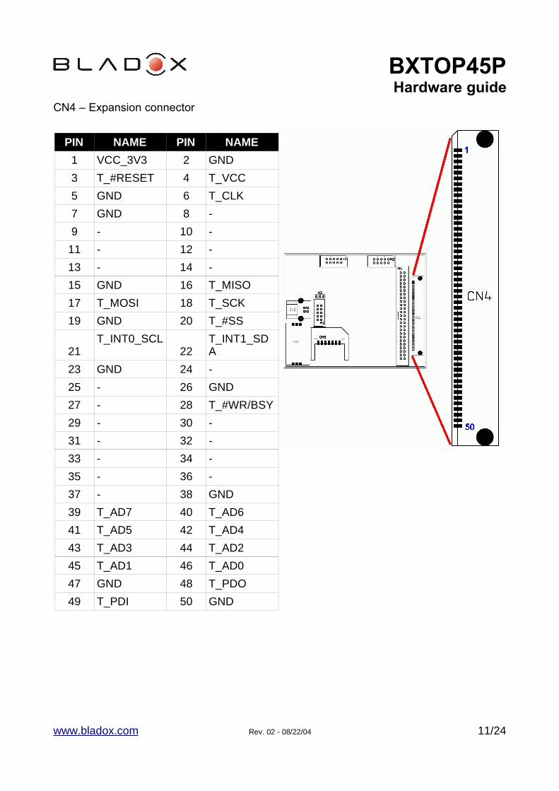
CN4 – Expansion connector
www.bladox.com Rev. 02 - 08/22/04 11/24
PIN NAME PIN NAME
1 VCC_3V3 2 GND
3 T_#RESET 4 T_VCC
5 GND 6 T_CLK
7 GND 8 -
9 - 10 -
11 - 12 -
13 - 14 -
15 GND 16 T_MISO
17 T_MOSI 18 T_SCK
19 GND 20 T_#SS
21T_INT0_SCL
22T_INT1_SDA
23 GND 24 -
25 - 26 GND
27 - 28 T_#WR/BSY
29 - 30 -
31 - 32 -
33 - 34 -
35 - 36 -
37 - 38 GND
39 T_AD7 40 T_AD6
41 T_AD5 42 T_AD4
43 T_AD3 44 T_AD2
45 T_AD1 46 T_AD0
47 GND 48 T_PDO
49 T_PDI 50 GND
BXTOP45PHardware guide
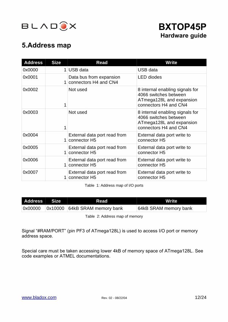
5.Address map
Address Size Read Write
0x0000 1 USB data USB data
0x00011
Data bus from expansionconnectors H4 and CN4
LED diodes
0x0002
1
Not used 8 internal enabling signals for4066 switches betweenATmega128L and expansionconnectors H4 and CN4
0x0003
1
Not used 8 internal enabling signals for4066 switches betweenATmega128L and expansionconnectors H4 and CN4
0x00041
External data port read fromconnector H5
External data port write toconnector H5
0x00051
External data port read fromconnector H5
External data port write toconnector H5
0x00061
External data port read fromconnector H5
External data port write toconnector H5
0x00071
External data port read fromconnector H5
External data port write toconnector H5
Table 1: Address map of I/O ports
Address Size Read Write
0x00000 0x10000 64kB SRAM memory bank 64kB SRAM memory bank
Table 2: Address map of memory
Signal “#RAM/PORT” (pin PF3 of ATmega128L) is used to access I/O port or memoryaddress space.
Special care must be taken accessing lower 4kB of memory space of ATmega128L. Seecode examples or ATMEL documentations.
www.bladox.com Rev. 02 - 08/22/04 12/24
BXTOP45PHardware guide
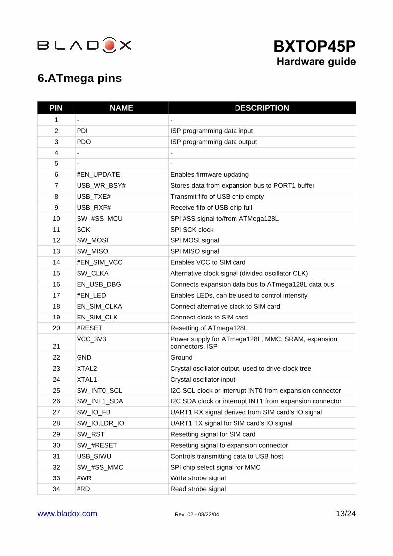
6.ATmega pins
PIN NAME DESCRIPTION1 - -
2 PDI ISP programming data input
3 PDO ISP programming data output
4 - -
5 - -
6 #EN_UPDATE Enables firmware updating
7 USB_WR_BSY# Stores data from expansion bus to PORT1 buffer
8 USB_TXE# Transmit fifo of USB chip empty
9 USB_RXF# Receive fifo of USB chip full
10 SW_#SS_MCU SPI #SS signal to/from ATMega128L
11 SCK SPI SCK clock
12 SW_MOSI SPI MOSI signal
13 SW_MISO SPI MISO signal
14 #EN_SIM_VCC Enables VCC to SIM card
15 SW_CLKA Alternative clock signal (divided oscillator CLK)
16 EN_USB_DBG Connects expansion data bus to ATmega128L data bus
17 #EN_LED Enables LEDs, can be used to control intensity
18 EN_SIM_CLKA Connect alternative clock to SIM card
19 EN_SIM_CLK Connect clock to SIM card
20 #RESET Resetting of ATmega128L
21VCC_3V3 Power supply for ATmega128L, MMC, SRAM, expansion
connectors, ISP
22 GND Ground
23 XTAL2 Crystal oscillator output, used to drive clock tree
24 XTAL1 Crystal oscillator input
25 SW_INT0_SCL I2C SCL clock or interrupt INT0 from expansion connector
26 SW_INT1_SDA I2C SDA clock or interrupt INT1 from expansion connector
27 SW_IO_FB UART1 RX signal derived from SIM card's IO signal
28 SW_IO,LDR_IO UART1 TX signal for SIM card's IO signal
29 SW_RST Resetting signal for SIM card
30 SW_#RESET Resetting signal to expansion connector
31 USB_SIWU Controls transmitting data to USB host
32 SW_#SS_MMC SPI chip select signal for MMC
33 #WR Write strobe signal
34 #RD Read strobe signal
www.bladox.com Rev. 02 - 08/22/04 13/24
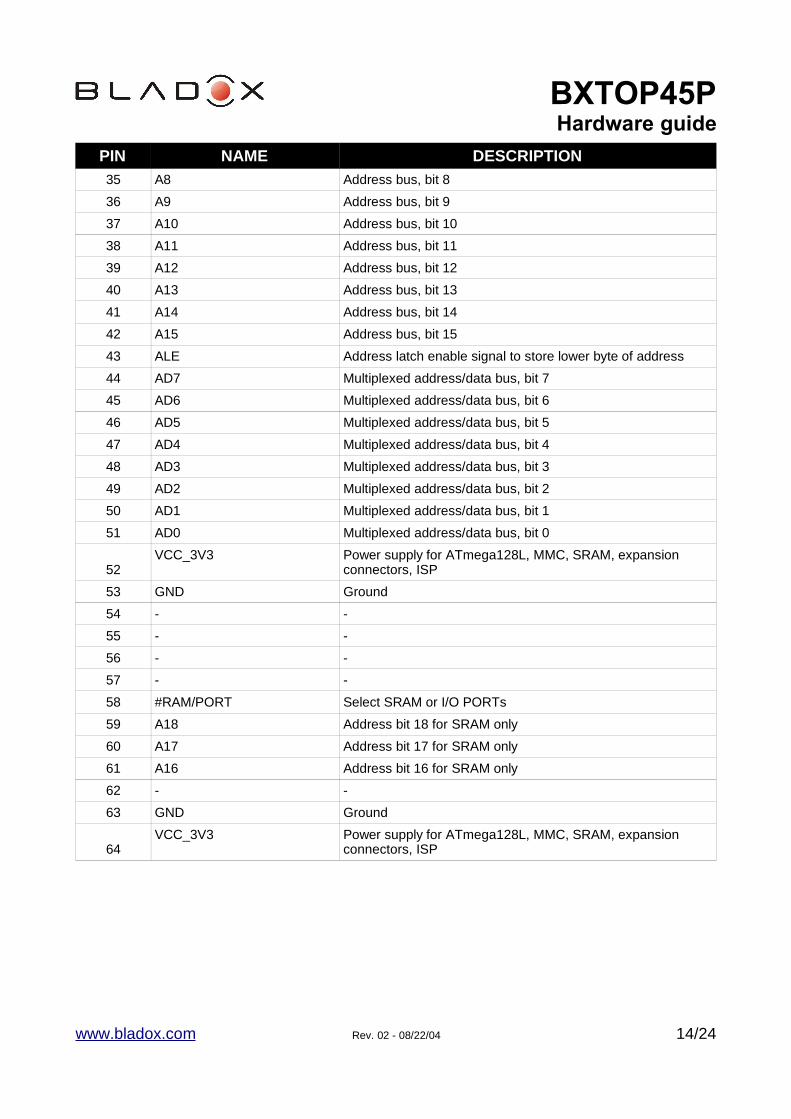
BXTOP45PHardware guide
PIN NAME DESCRIPTION35 A8 Address bus, bit 8
36 A9 Address bus, bit 9
37 A10 Address bus, bit 10
38 A11 Address bus, bit 11
39 A12 Address bus, bit 12
40 A13 Address bus, bit 13
41 A14 Address bus, bit 14
42 A15 Address bus, bit 15
43 ALE Address latch enable signal to store lower byte of address
44 AD7 Multiplexed address/data bus, bit 7
45 AD6 Multiplexed address/data bus, bit 6
46 AD5 Multiplexed address/data bus, bit 5
47 AD4 Multiplexed address/data bus, bit 4
48 AD3 Multiplexed address/data bus, bit 3
49 AD2 Multiplexed address/data bus, bit 2
50 AD1 Multiplexed address/data bus, bit 1
51 AD0 Multiplexed address/data bus, bit 0
52VCC_3V3 Power supply for ATmega128L, MMC, SRAM, expansion
connectors, ISP
53 GND Ground
54 - -
55 - -
56 - -
57 - -
58 #RAM/PORT Select SRAM or I/O PORTs
59 A18 Address bit 18 for SRAM only
60 A17 Address bit 17 for SRAM only
61 A16 Address bit 16 for SRAM only
62 - -
63 GND Ground
64VCC_3V3 Power supply for ATmega128L, MMC, SRAM, expansion
connectors, ISP
www.bladox.com Rev. 02 - 08/22/04 14/24
BXTOP45PHardware guide
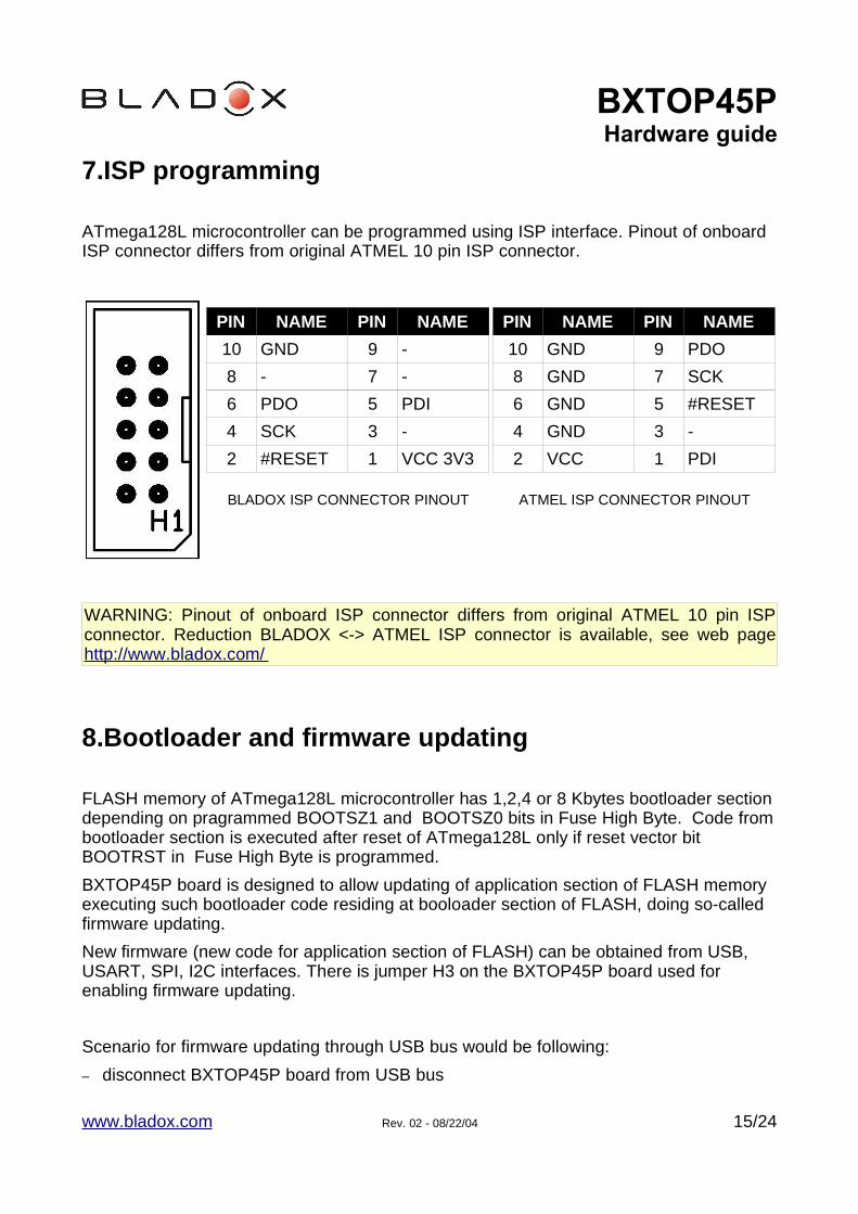
7.ISP programming
ATmega128L microcontroller can be programmed using ISP interface. Pinout of onboardISP connector differs from original ATMEL 10 pin ISP connector.
WARNING: Pinout of onboard ISP connector differs from original ATMEL 10 pin ISPconnector. Reduction BLADOX <-> ATMEL ISP connector is available, see web pagehttp://www.bladox.com/
8.Bootloader and firmware updating
FLASH memory of ATmega128L microcontroller has 1,2,4 or 8 Kbytes bootloader sectiondepending on pragrammed BOOTSZ1 and BOOTSZ0 bits in Fuse High Byte. Code frombootloader section is executed after reset of ATmega128L only if reset vector bitBOOTRST in Fuse High Byte is programmed.
BXTOP45P board is designed to allow updating of application section of FLASH memoryexecuting such bootloader code residing at booloader section of FLASH, doing so-calledfirmware updating.
New firmware (new code for application section of FLASH) can be obtained from USB,USART, SPI, I2C interfaces. There is jumper H3 on the BXTOP45P board used forenabling firmware updating.
Scenario for firmware updating through USB bus would be following:
– disconnect BXTOP45P board from USB bus
www.bladox.com Rev. 02 - 08/22/04 15/24
PIN NAME PIN NAME
10 GND 9 -
8 - 7 -
6 PDO 5 PDI
4 SCK 3 -
2 #RESET 1 VCC 3V3
BLADOX ISP CONNECTOR PINOUT
PIN NAME PIN NAME
10 GND 9 PDO
8 GND 7 SCK
6 GND 5 #RESET
4 GND 3 -
2 VCC 1 PDI
ATMEL ISP CONNECTOR PINOUT
BXTOP45PHardware guide
– set jumper H3 to 2-3 position (enable firmware updating)
– plug BXTOP45P into USB again (bootloader recognizes FW updating request)
– use utility for new firmware updating
Other scenarios of FW updating are possible depending on user needs.
NOTE: Visit web page http://www.bladox.com/ for bootloader examples.
9.Redefining USB device settings
BXTOP45P board uses FTDI's FT8U245BM chip as USB bus interface. BXTOP45P boardacts as USB device for USB host and its default USB parameters are stored inFT8U245BM chip. However user defined values for some of USB parameters canredefine default values. Such customization is made by attaching serial EEPROM toFT8U245BM chip and program it with the replacement parameters. FT8U245BM chipsupports direct programming of serial EEPROM over USB using a programming utility.
Following parameters can be redefined:USB Vendor ID and Product ID numbers, Self Powered or Bus Powered, CurrentConsumption, Manufacturer, Product Description, Serial Number.
NOTE: Go web page http://www.bladox.com/ to download EEPROM programming utilityto customize USB parameters of your BXTOP45P board.
10.Application examples
Application examples for USB , SIM, MMC and others will be available soon.
NOTE: Check web page http://www.bladox.com/ to download actual applicationexamples and application notes files.
www.bladox.com Rev. 02 - 08/22/04 16/24
BXTOP45PHardware guide
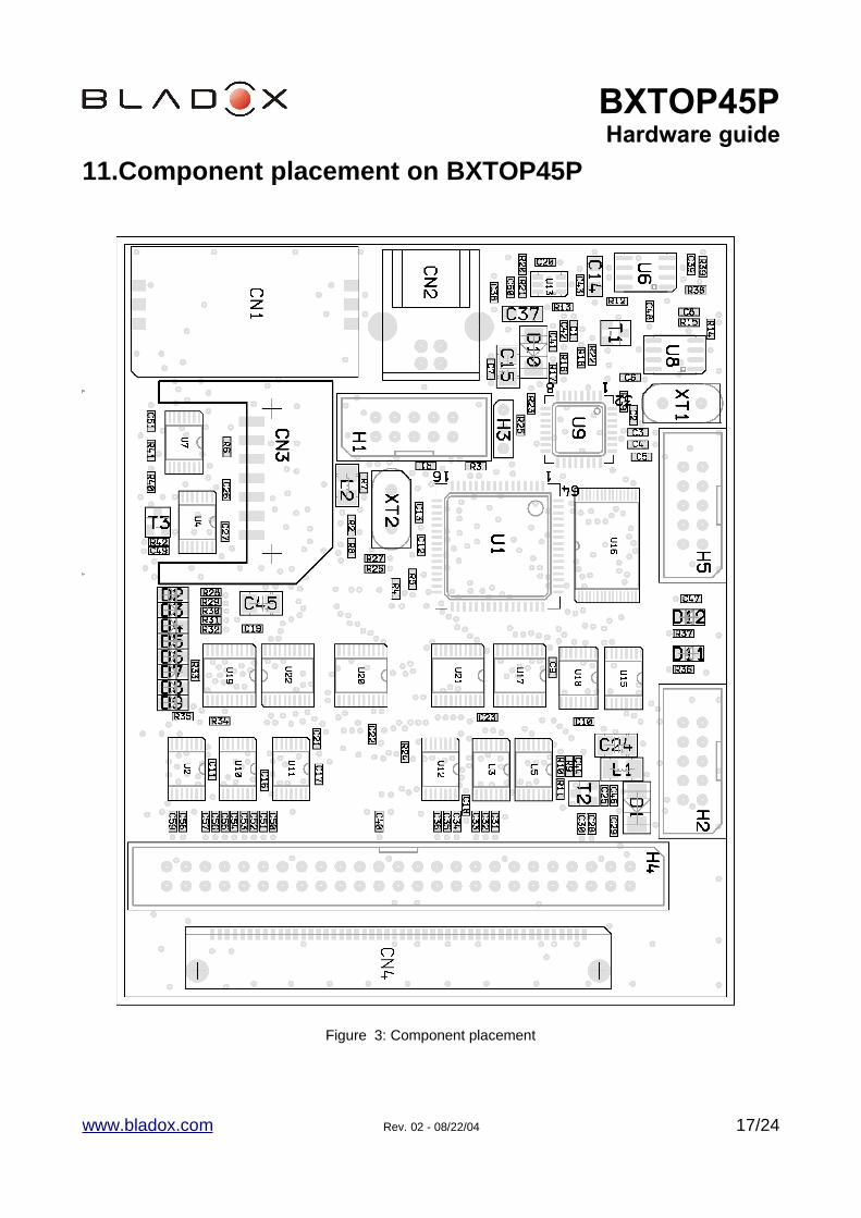
11.Component placement on BXTOP45P
www.bladox.com Rev. 02 - 08/22/04 17/24
Figure 3: Component placement
BXTOP45PHardware guide
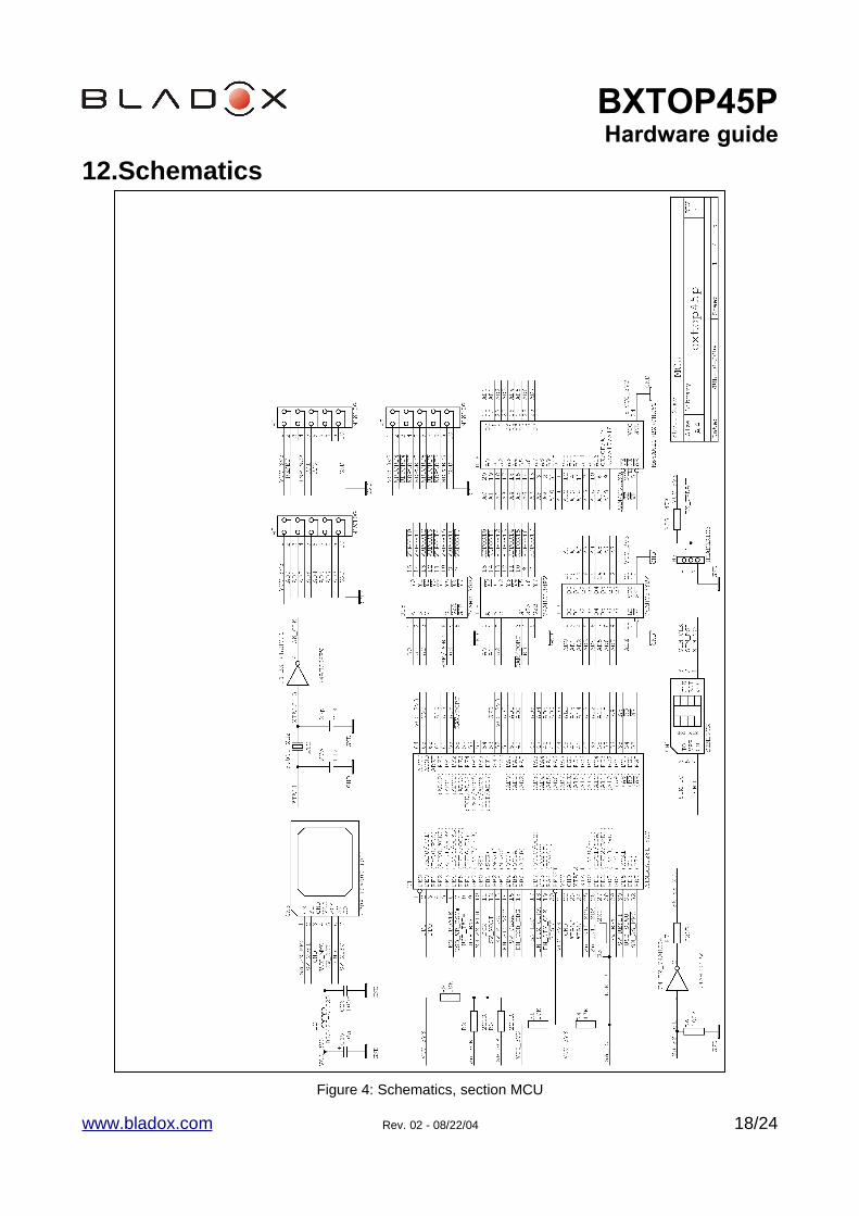
12.Schematics
www.bladox.com Rev. 02 - 08/22/04 18/24
Figure 4: Schematics, section MCU
BXTOP45PHardware guide
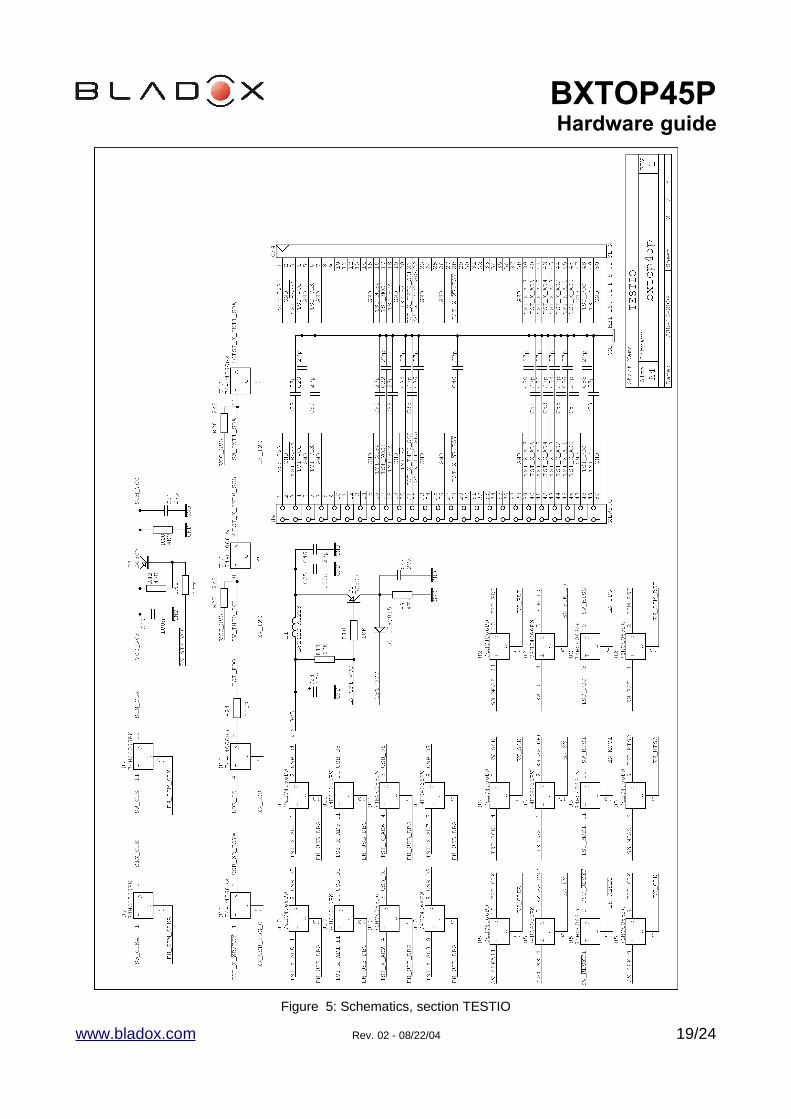
www.bladox.com Rev. 02 - 08/22/04 19/24
Figure 5: Schematics, section TESTIO
BXTOP45PHardware guide
www.bladox.com Rev. 02 - 08/22/04 20/24
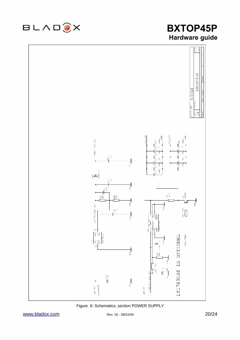
Figure 6: Schematics, section POWER SUPPLY
BXTOP45PHardware guide
www.bladox.com Rev. 02 - 08/22/04 21/24
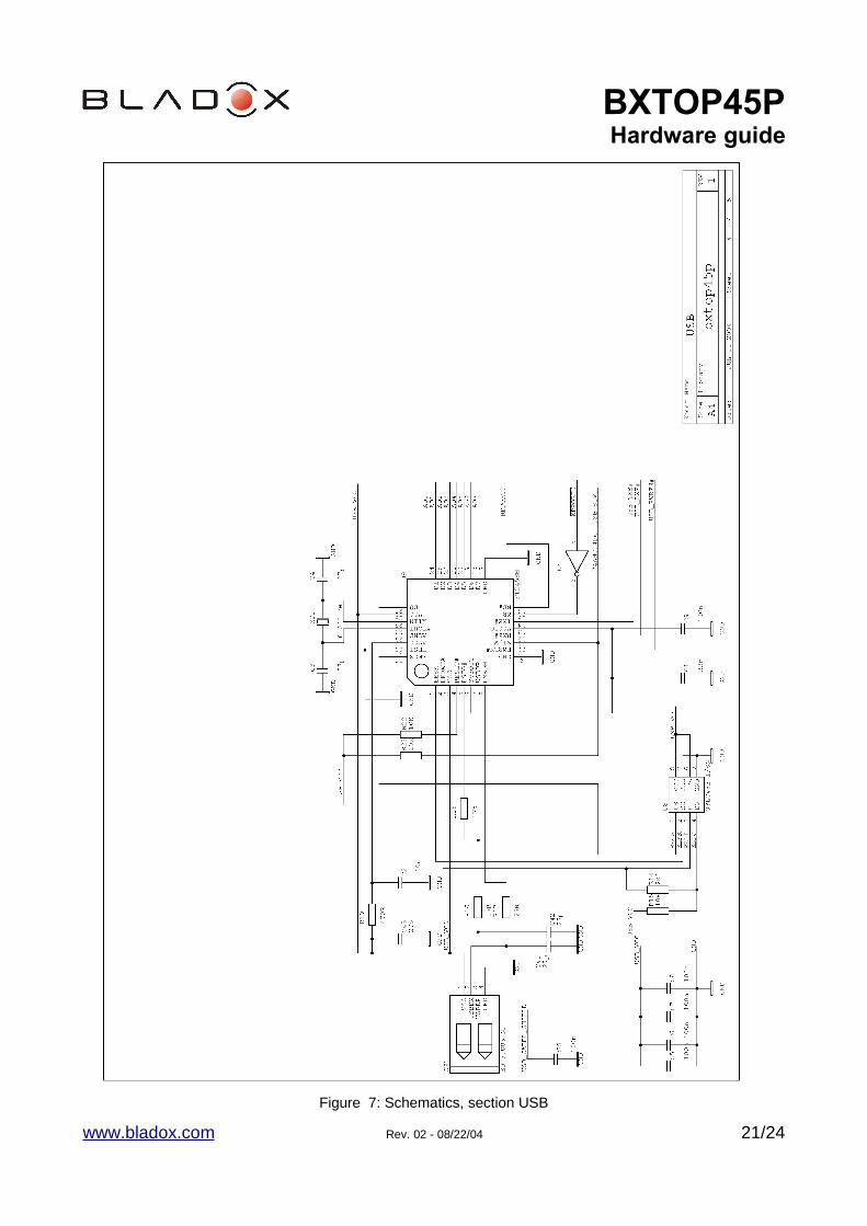
Figure 7: Schematics, section USB
BXTOP45PHardware guide
www.bladox.com Rev. 02 - 08/22/04 22/24
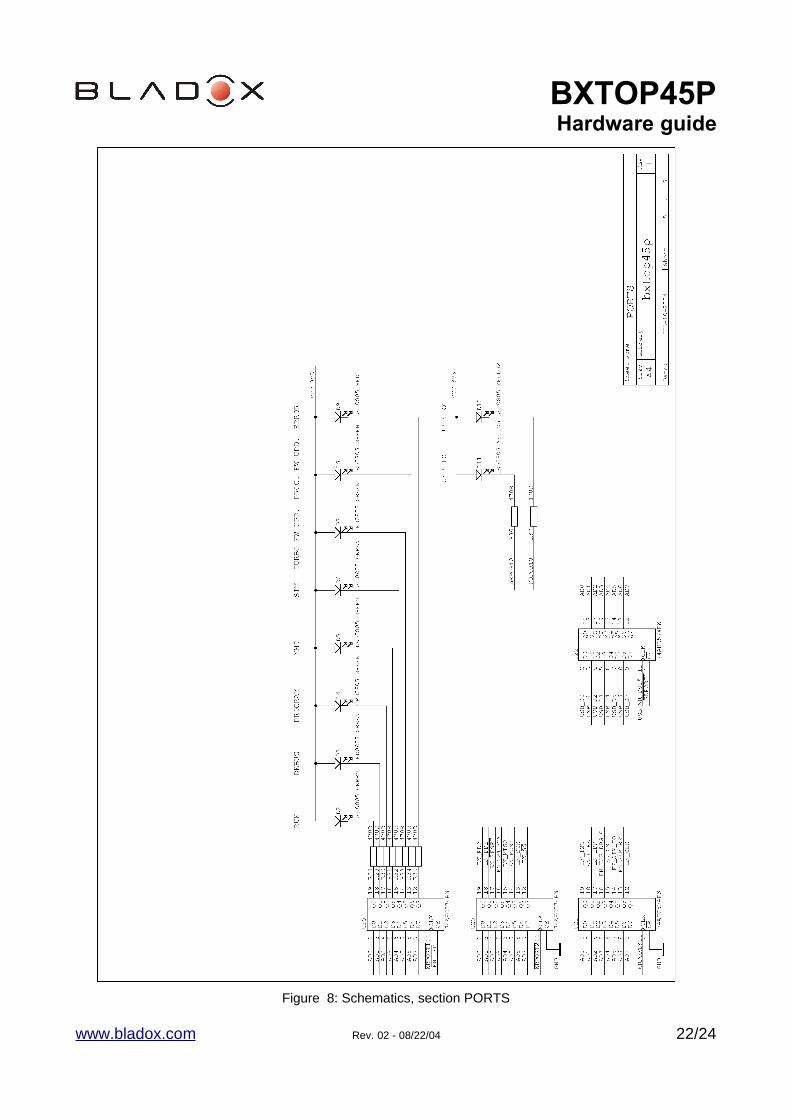
Figure 8: Schematics, section PORTS
BXTOP45PHardware guide
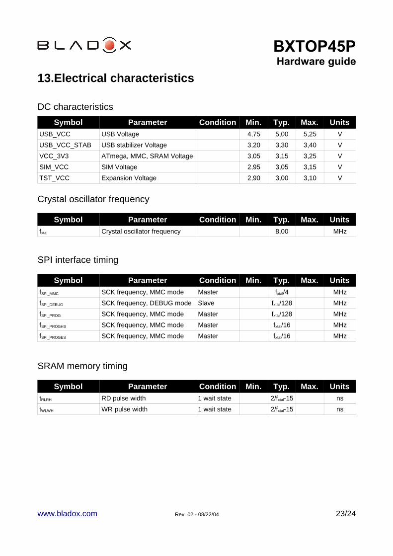
13.Electrical characteristics
DC characteristics
Symbol Parameter Condition Min. Typ. Max. UnitsUSB_VCC USB Voltage 4,75 5,00 5,25 V
USB_VCC_STAB USB stabilizer Voltage 3,20 3,30 3,40 V
VCC_3V3 ATmega, MMC, SRAM Voltage 3,05 3,15 3,25 V
SIM_VCC SIM Voltage 2,95 3,05 3,15 V
TST_VCC Expansion Voltage 2,90 3,00 3,10 V
Crystal oscillator frequency
Symbol Parameter Condition Min. Typ. Max. Unitsfxtal Crystal oscillator frequency 8,00 MHz
SPI interface timing
Symbol Parameter Condition Min. Typ. Max. UnitsfSPI_MMC SCK frequency, MMC mode Master fxtal/4 MHz
fSPI_DEBUG SCK frequency, DEBUG mode Slave fxtal/128 MHz
fSPI_PROG SCK frequency, MMC mode Master fxtal/128 MHz
fSPI_PROGHS SCK frequency, MMC mode Master fxtal/16 MHz
fSPI_PROGES SCK frequency, MMC mode Master fxtal/16 MHz
SRAM memory timing
Symbol Parameter Condition Min. Typ. Max. UnitstRLRH RD pulse width 1 wait state 2/fxtal-15 ns
tWLWH WR pulse width 1 wait state 2/fxtal-15 ns
www.bladox.com Rev. 02 - 08/22/04 23/24
BXTOP45PHardware guide
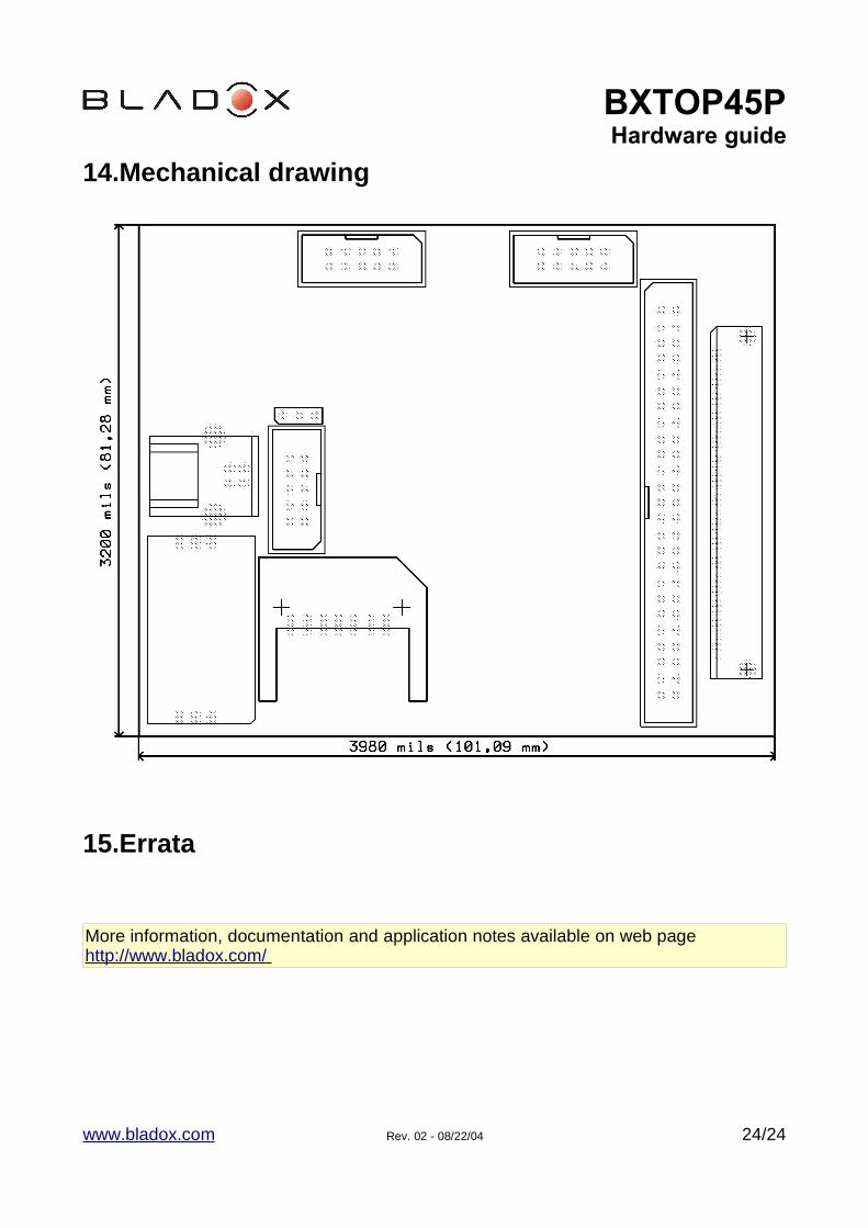
14.Mechanical drawing
15.Errata
More information, documentation and application notes available on web pagehttp://www.bladox.com/
www.bladox.com Rev. 02 - 08/22/04 24/24