Embed Size (px)
Citation preview
USB Hub
DP RX
TUSB1064
Typ
e-C
Re
ce
pta
cle
PD Controller
D+/-
SSRX
SSTX
DP0
DP1
DP2
DP3
AUXn
AUXp
SBU1
SBU2
CC1
CC2 Control
HPDCTL FLIP01
RX2
RX1
TX2
TX1
HPDIN
TUSB1064
Product
Folder
Order
Now
Technical
Documents
Tools &
Software
Support &Community
An IMPORTANT NOTICE at the end of this data sheet addresses availability, warranty, changes, use in safety-critical applications,intellectual property matters and other important disclaimers. PRODUCTION DATA.
TUSB1064SLLSF48C –MARCH 2018–REVISED SEPTEMBER 2019
TUSB1064 USB TYPE-C™ DP Alt Mode 10 Gbps Sink-Side Linear Redriver CrosspointSwitch
1
1 Features1• USB Type-C™ crosspoint switch supporting
– USB 3.1 Gen 2 + 2 DP 1.4 lanes– 4 DP 1.4 lanes
• USB 3.1 Gen 2 up to 10 Gbps• DisplayPort 1.4 up to 8.1 Gbps (HBR3)• VESA DisplayPort™ alt mode UFP_D redriving
crosspoint switch supporting c, d, and e pinassignments
• Ultra-low-power architecture• Linear redriver with up to 12 dB equalization• Transparent to DisplayPort link training• Automatic LFPS de-emphasis control to meet
USB 3.1 certification requirements• Configuration through GPIO or I2C• Hot-plug capable• Industrial temperature range: –40ºC to 85ºC
(TUSB1064I)• Commercial temperature range: 0ºC to 70ºC
(TUSB1064)• 4 mm x 6 mm, 0.4 mm Pitch WQFN package
2 Applications• Monitors• HDTV• Projectors• Docking stations
3 DescriptionThe TUSB1064 s a VESA USB Type-C™ Alt Moderedriving switch supporting USB 3.1 data rates up to10 Gbps and DisplayPort 1.4 up to 8.1 Gbps forupstream facing port (Sink). The device is used forUFP_D pin assignments C, D, and E from the VESADisplayPort Alt Mode on USB Type-C Standard.
The TUSB1064 provides several levels of receivelinear equalization to compensate for inter symbolinterference (ISI) due to cable and board trace loss.Operates on a single 3.3-V supply and comes in acommercial temperature range and industrialtemperature range.
Device Information(1)
PART NUMBER PACKAGE BODY SIZE (NOM)TUSB1064
WQFN (40) 4.00 mm x 6.00 mmTUSB1064I
(1) For all available packages, see the orderable addendum atthe end of the data sheet.
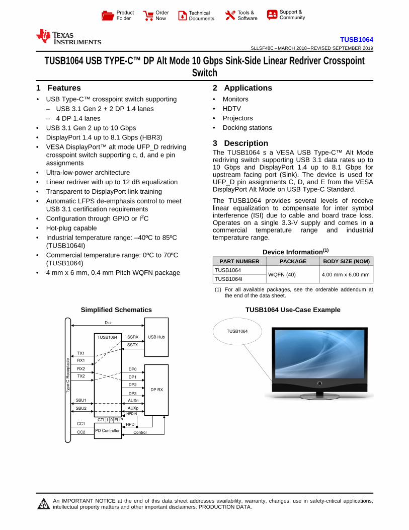
Simplified Schematics TUSB1064 Use-Case Example
2
TUSB1064SLLSF48C –MARCH 2018–REVISED SEPTEMBER 2019 www.ti.com
Product Folder Links: TUSB1064
Submit Documentation Feedback Copyright © 2018–2019, Texas Instruments Incorporated
Table of Contents1 Features .................................................................. 12 Applications ........................................................... 13 Description ............................................................. 14 Revision History..................................................... 25 Pin Configuration and Functions ......................... 36 Specifications......................................................... 5
6.1 Absolute Maximum Ratings ...................................... 56.2 ESD Ratings.............................................................. 56.3 Recommended Operating Conditions....................... 56.4 Thermal Information .................................................. 56.5 ELECTRICAL CHARACTERISTICS......................... 66.6 Switching Characteristics .......................................... 96.7 Timing Requirements .............................................. 106.8 Typical Characteristics ............................................ 11
7 Parameter Measurement Information ................ 138 Detailed Description ............................................ 15
8.1 Overview ................................................................. 158.2 Functional Block Diagram ....................................... 168.3 Feature Description................................................. 17
8.4 Device Functional Modes........................................ 188.5 Programming........................................................... 238.6 Register Maps ......................................................... 25
9 Application and Implementation ........................ 309.1 Application Information............................................ 309.2 Typical Application ................................................. 309.3 System Examples .................................................. 35
10 Power Supply Recommendations ..................... 4011 Layout................................................................... 41
11.1 Layout Guidelines ................................................. 4111.2 Layout Example .................................................... 41
12 Device and Documentation Support ................. 4212.1 Receiving Notification of Documentation Updates 4212.2 Community Resources.......................................... 4212.3 Trademarks ........................................................... 4212.4 Electrostatic Discharge Caution............................ 4212.5 Glossary ................................................................ 42
13 Mechanical, Packaging, and OrderableInformation ........................................................... 42
4 Revision HistoryNOTE: Page numbers for previous revisions may differ from page numbers in the current version.
Changes from Revision B (May 2019) to Revision C Page
• Added note to disable AUX snoop to resolve interop issues with a non-compliant AUX source. ....................................... 17
Changes from Revision A (November 2018) to Revision B Page
• Added following to pin 38 description: If I2C_EN = “F”, then this pin must be set to “F” or “0”. ........................................... 4• Changed GLF min, typ, and max from -1, 0, 1 to -2.5, 0.5, and 3.5 respectively. .................................................................. 8• Added GLF_LFPS_TX1/2 to AC electrical ...................................................................................................................................... 8
Changes from Original (March 2018) to Revision A Page
• Changed the RNQ pin image appearance ............................................................................................................................ 3• Changed the column on EN From: I To: 2 Level I (PD) ........................................................................................................ 4• Changed the EN pin Description in the Pin Functions table .................................................................................................. 4• Changed the HPDIN pin From: I/O To: 2 Level I .................................................................................................................. 4• Added pull-down indicator (PD) in the I/O column on FLIP/SCL and CTL0/SDA pins ......................................................... 4• Added Junction temperature to absolute maximum ratings table. ........................................................................................ 5• From: Internal pull-down resistance for CTL1. To: Internal pull-down resistance for CTL1, CTL0, FLIP, and EN. ........... 6• Deleted EN from Note 1 of Table 8 ..................................................................................................................................... 23
Thermal
Pad
1NC
2DPEQ1
3SSEQ1
4SSRXn
5SSRXp
6VCC
7SSTXn
8SSTXp
9T
X1
p
10
TX
1n
11
EQ
0
12
RX
1p
13
RX
1n
14
EQ
1
15
RX
2n
16
RX
2p
17
I2C
_E
N
18
TX
2n
19
TX
2p
20
VC
C
21 FLIP/SCL
22 CTL0/SDA
23 CTL1
24 SBU1
25 SBU2
26 AUXp
27 AUXn
28 VCC
29
EN
30
DP
3n
31
DP
3p
32
HP
DIN
33
DP
2n
34
DP
2p
35
DP
EQ
0/A
1
36
DP
1n
37
DP
1p
38
SS
EQ
0/A
0
39
DP
0n
40
DP
0p
Not to scale
3
TUSB1064www.ti.com SLLSF48C –MARCH 2018–REVISED SEPTEMBER 2019
Product Folder Links: TUSB1064
Submit Documentation FeedbackCopyright © 2018–2019, Texas Instruments Incorporated
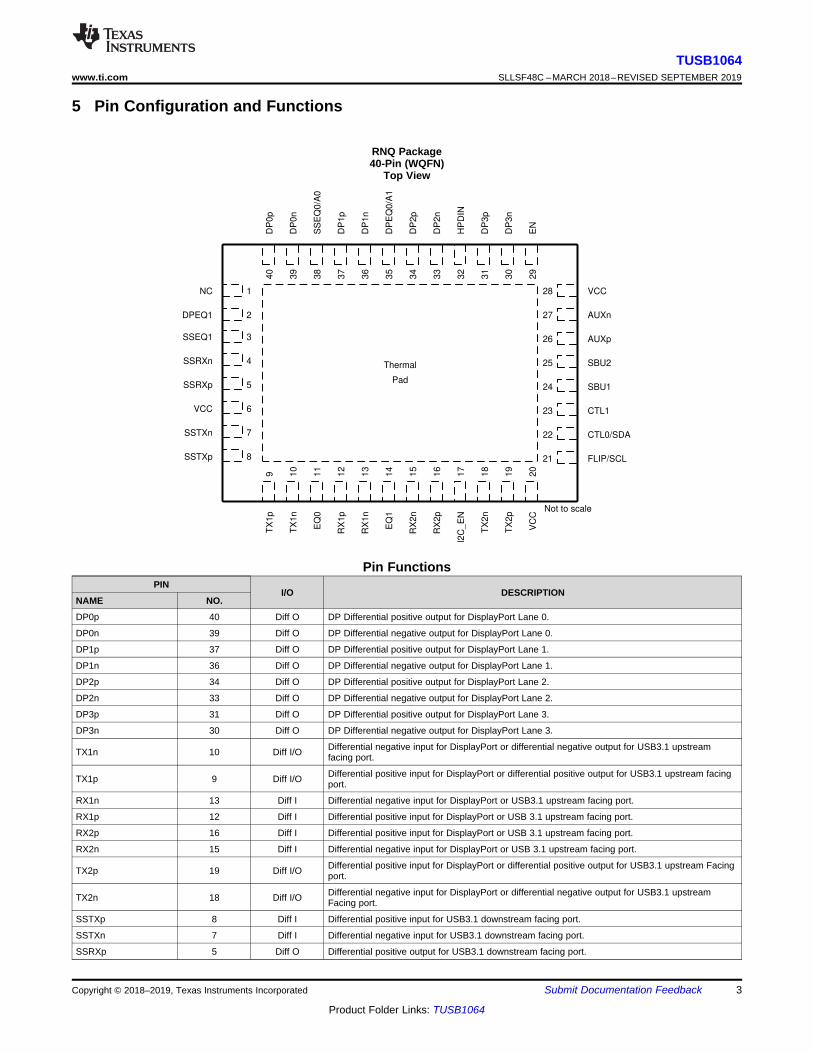
5 Pin Configuration and Functions
RNQ Package40-Pin (WQFN)
Top View
Pin FunctionsPIN
I/O DESCRIPTIONNAME NO.
DP0p 40 Diff O DP Differential positive output for DisplayPort Lane 0.
DP0n 39 Diff O DP Differential negative output for DisplayPort Lane 0.
DP1p 37 Diff O DP Differential positive output for DisplayPort Lane 1.
DP1n 36 Diff O DP Differential negative output for DisplayPort Lane 1.
DP2p 34 Diff O DP Differential positive output for DisplayPort Lane 2.
DP2n 33 Diff O DP Differential negative output for DisplayPort Lane 2.
DP3p 31 Diff O DP Differential positive output for DisplayPort Lane 3.
DP3n 30 Diff O DP Differential negative output for DisplayPort Lane 3.
TX1n 10 Diff I/O Differential negative input for DisplayPort or differential negative output for USB3.1 upstreamfacing port.
TX1p 9 Diff I/O Differential positive input for DisplayPort or differential positive output for USB3.1 upstream facingport.
RX1n 13 Diff I Differential negative input for DisplayPort or USB3.1 upstream facing port.
RX1p 12 Diff I Differential positive input for DisplayPort or USB 3.1 upstream facing port.
RX2p 16 Diff I Differential positive input for DisplayPort or USB 3.1 upstream facing port.
RX2n 15 Diff I Differential negative input for DisplayPort or USB 3.1 upstream facing port.
TX2p 19 Diff I/O Differential positive input for DisplayPort or differential positive output for USB3.1 upstream Facingport.
TX2n 18 Diff I/O Differential negative input for DisplayPort or differential negative output for USB3.1 upstreamFacing port.
SSTXp 8 Diff I Differential positive input for USB3.1 downstream facing port.
SSTXn 7 Diff I Differential negative input for USB3.1 downstream facing port.
SSRXp 5 Diff O Differential positive output for USB3.1 downstream facing port.
4
TUSB1064SLLSF48C –MARCH 2018–REVISED SEPTEMBER 2019 www.ti.com
Product Folder Links: TUSB1064
Submit Documentation Feedback Copyright © 2018–2019, Texas Instruments Incorporated
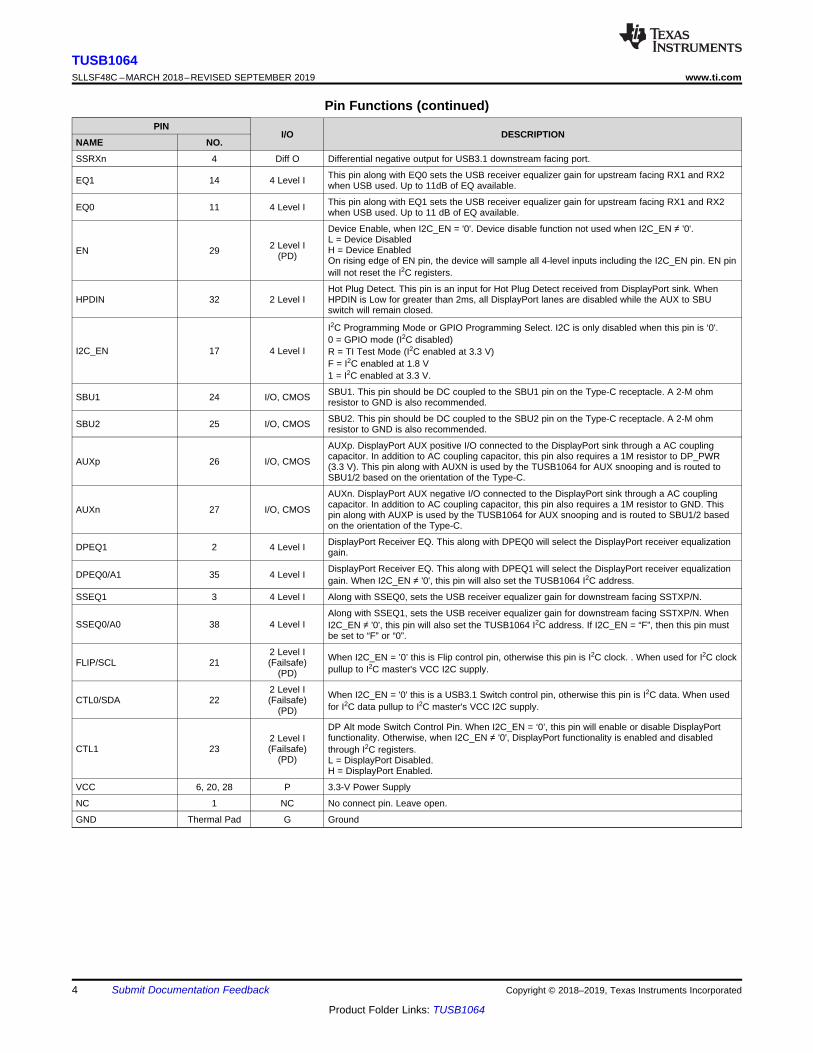
Pin Functions (continued)PIN
I/O DESCRIPTIONNAME NO.
SSRXn 4 Diff O Differential negative output for USB3.1 downstream facing port.
EQ1 14 4 Level I This pin along with EQ0 sets the USB receiver equalizer gain for upstream facing RX1 and RX2when USB used. Up to 11dB of EQ available.
EQ0 11 4 Level I This pin along with EQ1 sets the USB receiver equalizer gain for upstream facing RX1 and RX2when USB used. Up to 11 dB of EQ available.
EN 29 2 Level I(PD)
Device Enable, when I2C_EN = '0'. Device disable function not used when I2C_EN ≠ '0'.L = Device DisabledH = Device EnabledOn rising edge of EN pin, the device will sample all 4-level inputs including the I2C_EN pin. EN pinwill not reset the I2C registers.
HPDIN 32 2 Level IHot Plug Detect. This pin is an input for Hot Plug Detect received from DisplayPort sink. WhenHPDIN is Low for greater than 2ms, all DisplayPort lanes are disabled while the AUX to SBUswitch will remain closed.
I2C_EN 17 4 Level I
I2C Programming Mode or GPIO Programming Select. I2C is only disabled when this pin is ‘0'.0 = GPIO mode (I2C disabled)R = TI Test Mode (I2C enabled at 3.3 V)F = I2C enabled at 1.8 V1 = I2C enabled at 3.3 V.
SBU1 24 I/O, CMOS SBU1. This pin should be DC coupled to the SBU1 pin on the Type-C receptacle. A 2-M ohmresistor to GND is also recommended.
SBU2 25 I/O, CMOS SBU2. This pin should be DC coupled to the SBU2 pin on the Type-C receptacle. A 2-M ohmresistor to GND is also recommended.
AUXp 26 I/O, CMOS
AUXp. DisplayPort AUX positive I/O connected to the DisplayPort sink through a AC couplingcapacitor. In addition to AC coupling capacitor, this pin also requires a 1M resistor to DP_PWR(3.3 V). This pin along with AUXN is used by the TUSB1064 for AUX snooping and is routed toSBU1/2 based on the orientation of the Type-C.
AUXn 27 I/O, CMOS
AUXn. DisplayPort AUX negative I/O connected to the DisplayPort sink through a AC couplingcapacitor. In addition to AC coupling capacitor, this pin also requires a 1M resistor to GND. Thispin along with AUXP is used by the TUSB1064 for AUX snooping and is routed to SBU1/2 basedon the orientation of the Type-C.
DPEQ1 2 4 Level I DisplayPort Receiver EQ. This along with DPEQ0 will select the DisplayPort receiver equalizationgain.
DPEQ0/A1 35 4 Level I DisplayPort Receiver EQ. This along with DPEQ1 will select the DisplayPort receiver equalizationgain. When I2C_EN ≠ '0', this pin will also set the TUSB1064 I2C address.
SSEQ1 3 4 Level I Along with SSEQ0, sets the USB receiver equalizer gain for downstream facing SSTXP/N.
SSEQ0/A0 38 4 Level IAlong with SSEQ1, sets the USB receiver equalizer gain for downstream facing SSTXP/N. WhenI2C_EN ≠ '0', this pin will also set the TUSB1064 I2C address. If I2C_EN = “F”, then this pin mustbe set to “F” or “0”.
FLIP/SCL 212 Level I(Failsafe)
(PD)
When I2C_EN = ’0’ this is Flip control pin, otherwise this pin is I2C clock. . When used for I2C clockpullup to I2C master's VCC I2C supply.
CTL0/SDA 222 Level I(Failsafe)
(PD)
When I2C_EN = '0' this is a USB3.1 Switch control pin, otherwise this pin is I2C data. When usedfor I2C data pullup to I2C master's VCC I2C supply.
CTL1 232 Level I(Failsafe)
(PD)
DP Alt mode Switch Control Pin. When I2C_EN = ‘0’, this pin will enable or disable DisplayPortfunctionality. Otherwise, when I2C_EN ≠ '0', DisplayPort functionality is enabled and disabledthrough I2C registers.L = DisplayPort Disabled.H = DisplayPort Enabled.
VCC 6, 20, 28 P 3.3-V Power Supply
NC 1 NC No connect pin. Leave open.
GND Thermal Pad G Ground
5
TUSB1064www.ti.com SLLSF48C –MARCH 2018–REVISED SEPTEMBER 2019
Product Folder Links: TUSB1064
Submit Documentation FeedbackCopyright © 2018–2019, Texas Instruments Incorporated
(1) Stresses beyond those listed under Absolute Maximum Rating may cause permanent damage to the device. These are stress ratingsonly, which do not imply functional operation of the device at these or any other conditions beyond those indicated under RecommendedOperating Condition. Exposure to absolute-maximum-rated conditions for extended periods may affect device reliability.
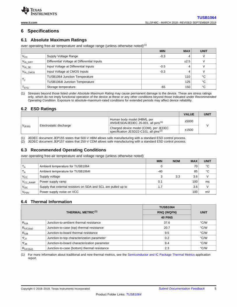
6 Specifications
6.1 Absolute Maximum Ratingsover operating free-air temperature and voltage range (unless otherwise noted) (1)
MIN MAX UNITVCC Supply Voltage Range -0.3 4 VVIN_DIFF Differential Voltage at Differential Inputs ±2.5 VVIN_SE Input Voltage at Differential Inputs -0.5 4 VVIN_CMOS Input Voltage at CMOS Inputs -0.3 4 V
TJTUSB1064 Junction Temperature 110 °CTUSB1064I Junction Temperature 125 °C
TSTG Storage temperature -65 150 °C
(1) JEDEC document JEP155 states that 500-V HBM allows safe manufacturing with a standard ESD control process.(2) JEDEC document JEP157 states that 250-V CDM allows safe manufacturing with a standard ESD control process.
6.2 ESD RatingsVALUE UNIT
V(ESD) Electrostatic discharge
Human body model (HBM), perANSI/ESDA/JEDEC JS-001, all pins (1) ±5000
VCharged device model (CDM), per JEDECspecification JESD22-C101, all pins (2) ±1500
6.3 Recommended Operating Conditionsover operating free-air temperature and voltage range (unless otherwise noted)
MIN NOM MAX UNITTA Ambient temperature for TUSB1064 0 70 °CTA Ambient temperature for TUSB1064I -40 85 °CVCC Supply voltage 3 3.3 3.6 VVCC_RAMP Power supply ramp 0.1 100 msVI2C Supply that external resistors on SDA and SCL are pulled up to 1.7 3.6 VVPSN Power supply noise on VCC 100 mV
(1) For more information about traditional and new thermal metrics, see the Semiconductor and IC Package Thermal Metrics applicationreport.
6.4 Thermal Information
THERMAL METRIC (1)TUSB1064
UNITRNQ (WQFN)40 PINS
RθJA Junction-to-ambient thermal resistance 37.6 °C/WRθJC(top) Junction-to-case (top) thermal resistance 20.7 °C/WRθJB Junction-to-board thermal resistance 9.5 °C/WΨJT Junction-to-top characterization parameter 0.2 °C/WΨJB Junction-to-board characterization parameter 9.4 °C/WRθJC(bot) Junction-to-case (bottom) thermal resistance 2.3 °C/W
6
TUSB1064SLLSF48C –MARCH 2018–REVISED SEPTEMBER 2019 www.ti.com
Product Folder Links: TUSB1064
Submit Documentation Feedback Copyright © 2018–2019, Texas Instruments Incorporated
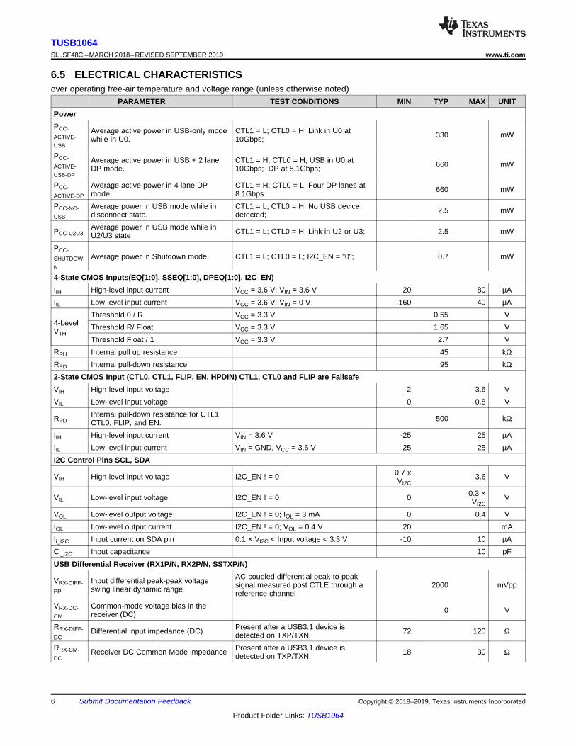
6.5 ELECTRICAL CHARACTERISTICSover operating free-air temperature and voltage range (unless otherwise noted)
PARAMETER TEST CONDITIONS MIN TYP MAX UNITPowerPCC-ACTIVE-USB
Average active power in USB-only modewhile in U0.
CTL1 = L; CTL0 = H; Link in U0 at10Gbps; 330 mW
PCC-ACTIVE-USB-DP
Average active power in USB + 2 laneDP mode.
CTL1 = H; CTL0 = H; USB in U0 at10Gbps; DP at 8.1Gbps; 660 mW
PCC-ACTIVE-DP
Average active power in 4 lane DPmode.
CTL1 = H; CTL0 = L; Four DP lanes at8.1Gbps 660 mW
PCC-NC-USB
Average power in USB mode while indisconnect state.
CTL1 = L; CTL0 = H; No USB devicedetected; 2.5 mW
PCC-U2U3Average power in USB mode while inU2/U3 state CTL1 = L; CTL0 = H; Link in U2 or U3; 2.5 mW
PCC-SHUTDOWN
Average power in Shutdown mode. CTL1 = L; CTL0 = L; I2C_EN = "0"; 0.7 mW
4-State CMOS Inputs(EQ[1:0], SSEQ[1:0], DPEQ[1:0], I2C_EN)IIH High-level input current VCC = 3.6 V; VIN = 3.6 V 20 80 µAIIL Low-level input current VCC = 3.6 V; VIN = 0 V -160 -40 µA
4-LevelVTH
Threshold 0 / R VCC = 3.3 V 0.55 VThreshold R/ Float VCC = 3.3 V 1.65 VThreshold Float / 1 VCC = 3.3 V 2.7 V
RPU Internal pull up resistance 45 kΩRPD Internal pull-down resistance 95 kΩ2-State CMOS Input (CTL0, CTL1, FLIP, EN, HPDIN) CTL1, CTL0 and FLIP are FailsafeVIH High-level input voltage 2 3.6 VVIL Low-level input voltage 0 0.8 V
RPDInternal pull-down resistance for CTL1,CTL0, FLIP, and EN. 500 kΩ
IIH High-level input current VIN = 3.6 V -25 25 µAIIL Low-level input current VIN = GND, VCC = 3.6 V -25 25 µAI2C Control Pins SCL, SDA
VIH High-level input voltage I2C_EN ! = 0 0.7 xVI2C
3.6 V
VIL Low-level input voltage I2C_EN ! = 0 0 0.3 ×VI2C
V
VOL Low-level output voltage I2C_EN ! = 0; IOL = 3 mA 0 0.4 VIOL Low-level output current I2C_EN ! = 0; VOL = 0.4 V 20 mAIi_I2C Input current on SDA pin 0.1 × VI2C < Input voltage < 3.3 V -10 10 µACi_I2C Input capacitance 10 pFUSB Differential Receiver (RX1P/N, RX2P/N, SSTXP/N)
VRX-DIFF-PP
Input differential peak-peak voltageswing linear dynamic range
AC-coupled differential peak-to-peaksignal measured post CTLE through areference channel
2000 mVpp
VRX-DC-CM
Common-mode voltage bias in thereceiver (DC) 0 V
RRX-DIFF-DC
Differential input impedance (DC) Present after a USB3.1 device isdetected on TXP/TXN 72 120 Ω
RRX-CM-DC
Receiver DC Common Mode impedance Present after a USB3.1 device isdetected on TXP/TXN 18 30 Ω
7
TUSB1064www.ti.com SLLSF48C –MARCH 2018–REVISED SEPTEMBER 2019
Product Folder Links: TUSB1064
Submit Documentation FeedbackCopyright © 2018–2019, Texas Instruments Incorporated
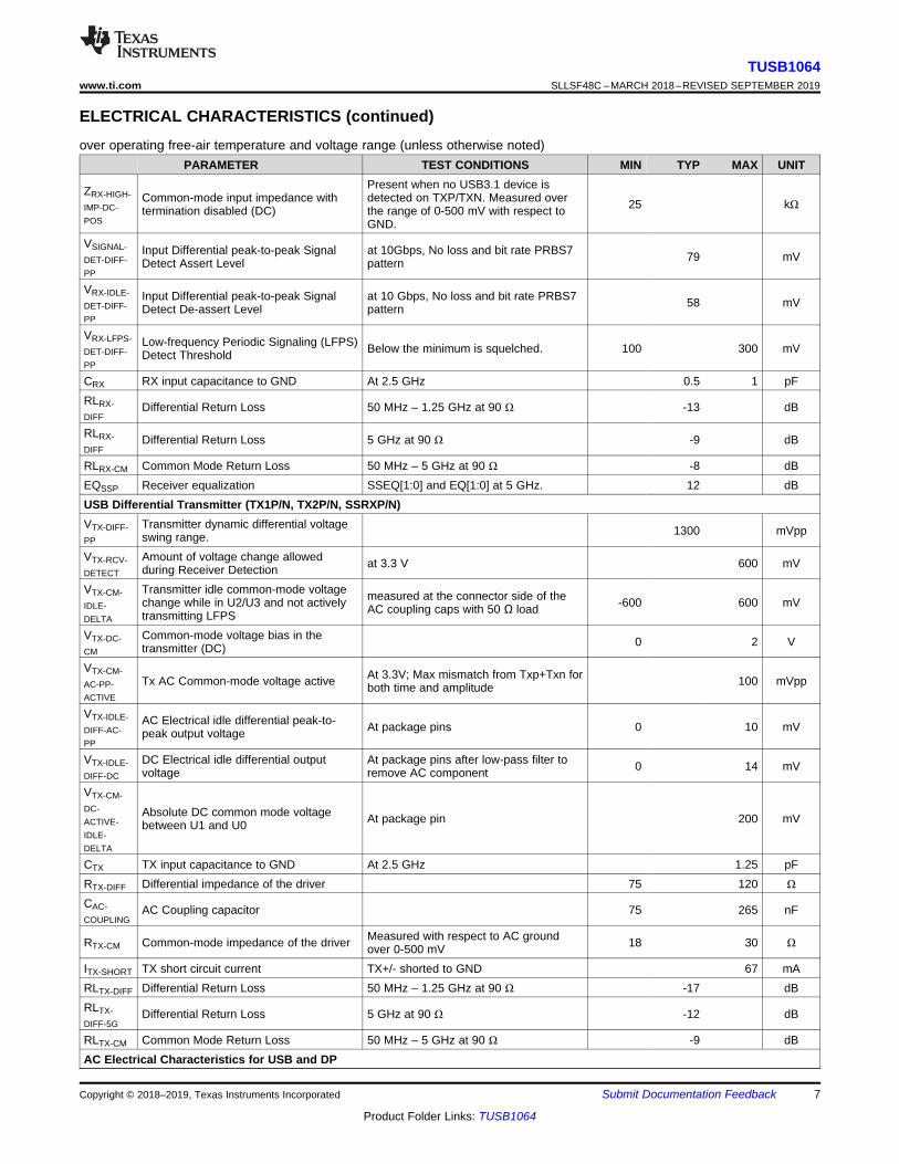
ELECTRICAL CHARACTERISTICS (continued)over operating free-air temperature and voltage range (unless otherwise noted)
PARAMETER TEST CONDITIONS MIN TYP MAX UNIT
ZRX-HIGH-IMP-DC-POS
Common-mode input impedance withtermination disabled (DC)
Present when no USB3.1 device isdetected on TXP/TXN. Measured overthe range of 0-500 mV with respect toGND.
25 kΩ
VSIGNAL-DET-DIFF-PP
Input Differential peak-to-peak SignalDetect Assert Level
at 10Gbps, No loss and bit rate PRBS7pattern 79 mV
VRX-IDLE-DET-DIFF-PP
Input Differential peak-to-peak SignalDetect De-assert Level
at 10 Gbps, No loss and bit rate PRBS7pattern 58 mV
VRX-LFPS-DET-DIFF-PP
Low-frequency Periodic Signaling (LFPS)Detect Threshold Below the minimum is squelched. 100 300 mV
CRX RX input capacitance to GND At 2.5 GHz 0.5 1 pFRLRX-DIFF
Differential Return Loss 50 MHz – 1.25 GHz at 90 Ω -13 dB
RLRX-DIFF
Differential Return Loss 5 GHz at 90 Ω -9 dB
RLRX-CM Common Mode Return Loss 50 MHz – 5 GHz at 90 Ω -8 dBEQSSP Receiver equalization SSEQ[1:0] and EQ[1:0] at 5 GHz. 12 dBUSB Differential Transmitter (TX1P/N, TX2P/N, SSRXP/N)VTX-DIFF-PP
Transmitter dynamic differential voltageswing range. 1300 mVpp
VTX-RCV-DETECT
Amount of voltage change allowedduring Receiver Detection at 3.3 V 600 mV
VTX-CM-IDLE-DELTA
Transmitter idle common-mode voltagechange while in U2/U3 and not activelytransmitting LFPS
measured at the connector side of theAC coupling caps with 50 Ω load -600 600 mV
VTX-DC-CM
Common-mode voltage bias in thetransmitter (DC) 0 2 V
VTX-CM-AC-PP-ACTIVE
Tx AC Common-mode voltage active At 3.3V; Max mismatch from Txp+Txn forboth time and amplitude 100 mVpp
VTX-IDLE-DIFF-AC-PP
AC Electrical idle differential peak-to-peak output voltage At package pins 0 10 mV
VTX-IDLE-DIFF-DC
DC Electrical idle differential outputvoltage
At package pins after low-pass filter toremove AC component 0 14 mV
VTX-CM-DC-ACTIVE-IDLE-DELTA
Absolute DC common mode voltagebetween U1 and U0 At package pin 200 mV
CTX TX input capacitance to GND At 2.5 GHz 1.25 pFRTX-DIFF Differential impedance of the driver 75 120 Ω
CAC-COUPLING
AC Coupling capacitor 75 265 nF
RTX-CM Common-mode impedance of the driver Measured with respect to AC groundover 0-500 mV 18 30 Ω
ITX-SHORT TX short circuit current TX+/- shorted to GND 67 mARLTX-DIFF Differential Return Loss 50 MHz – 1.25 GHz at 90 Ω -17 dBRLTX-DIFF-5G
Differential Return Loss 5 GHz at 90 Ω -12 dB
RLTX-CM Common Mode Return Loss 50 MHz – 5 GHz at 90 Ω -9 dBAC Electrical Characteristics for USB and DP
8
TUSB1064SLLSF48C –MARCH 2018–REVISED SEPTEMBER 2019 www.ti.com
Product Folder Links: TUSB1064
Submit Documentation Feedback Copyright © 2018–2019, Texas Instruments Incorporated
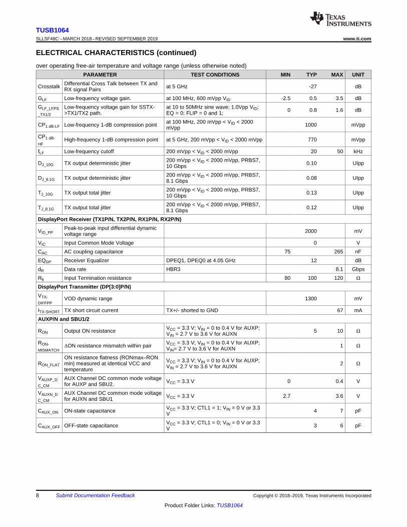
ELECTRICAL CHARACTERISTICS (continued)over operating free-air temperature and voltage range (unless otherwise noted)
PARAMETER TEST CONDITIONS MIN TYP MAX UNIT
Crosstalk Differential Cross Talk between TX andRX signal Pairs at 5 GHz -27 dB
GLF Low-frequency voltage gain. at 100 MHz, 600 mVpp VID -2.5 0.5 3.5 dBGLF_LFPS_TX1/2
Low-frequency voltage gain for SSTX->TX1/TX2 path.
at 10 to 50MHz sine wave; 1.0Vpp VID;EQ = 0; FLIP = 0 and 1; 0 0.8 1.6 dB
CP1 dB-LF Low-frequency 1-dB compression point at 100 MHz, 200 mVpp < VID < 2000mVpp 1000 mVpp
CP1 dB-HF
High-frequency 1-dB compression point at 5 GHz, 200 mVpp < VID < 2000 mVpp 770 mVpp
fLF Low-frequency cutoff 200 mVpp < VID < 2000 mVpp 20 50 kHz
DJ_10G TX output deterministic jitter 200 mVpp < VID < 2000 mVpp, PRBS7,10 Gbps 0.10 UIpp
DJ_8.1G TX output deterministic jitter 200 mVpp < VID < 2000 mVpp, PRBS7,8.1 Gbps 0.08 UIpp
TJ_10G TX output total jitter 200 mVpp < VID < 2000 mVpp, PRBS7,10 Gbps 0.13 UIpp
TJ_8.1G TX output total jitter 200 mVpp < VID < 2000 mVpp, PRBS7,8.1 Gbps 0.12 UIpp
DisplayPort Receiver (TX1P/N, TX2P/N, RX1P/N, RX2P/N)
VID_PPPeak-to-peak input differential dynamicvoltage range 2000 mV
VIC Input Common Mode Voltage 0 VCAC AC coupling capacitance 75 265 nFEQDP Receiver Equalizer DPEQ1, DPEQ0 at 4.05 GHz 12 dBdR Data rate HBR3 8.1 GbpsRti Input Termination resistance 80 100 120 Ω
DisplayPort Transmitter (DP[3:0]P/N)VTX-DIFFPP
VOD dynamic range 1300 mV
ITX-SHORT TX short circuit current TX+/- shorted to GND 67 mAAUXP/N and SBU1/2
RON Output ON resistance VCC = 3.3 V; VIN = 0 to 0.4 V for AUXP;VIN = 2.7 V to 3.6 V for AUXN 5 10 Ω
RON-MISMATCH
ΔON resistance mismatch within pair VCC = 3.3 V; VIN = 0 to 0.4 V for AUXP;VIN= 2.7 V to 3.6 V for AUXN 1 Ω
RON_FLAT
ON resistance flatness (RONmax–RONmin) measured at identical VCC andtemperature
VCC = 3.3 V; VIN = 0 to 0.4 V for AUXP;VIN = 2.7 V to 3.6 V for AUXN 2 Ω
VAUXP_DC_CM
AUX Channel DC common mode voltagefor AUXP and SBU2. VCC = 3.3 V 0 0.4 V
VAUXN_DC_CM
AUX Channel DC common mode voltagefor AUXN and SBU1 VCC = 3.3 V 2.7 3.6 V
CAUX_ON ON-state capacitance VCC = 3.3 V; CTL1 = 1; VIN = 0 V or 3.3V 4 7 pF
CAUX_OFF OFF-state capacitance VCC = 3.3 V; CTL1 = 0; VIN = 0 V or 3.3V 3 6 pF
9
TUSB1064www.ti.com SLLSF48C –MARCH 2018–REVISED SEPTEMBER 2019
Product Folder Links: TUSB1064
Submit Documentation FeedbackCopyright © 2018–2019, Texas Instruments Incorporated
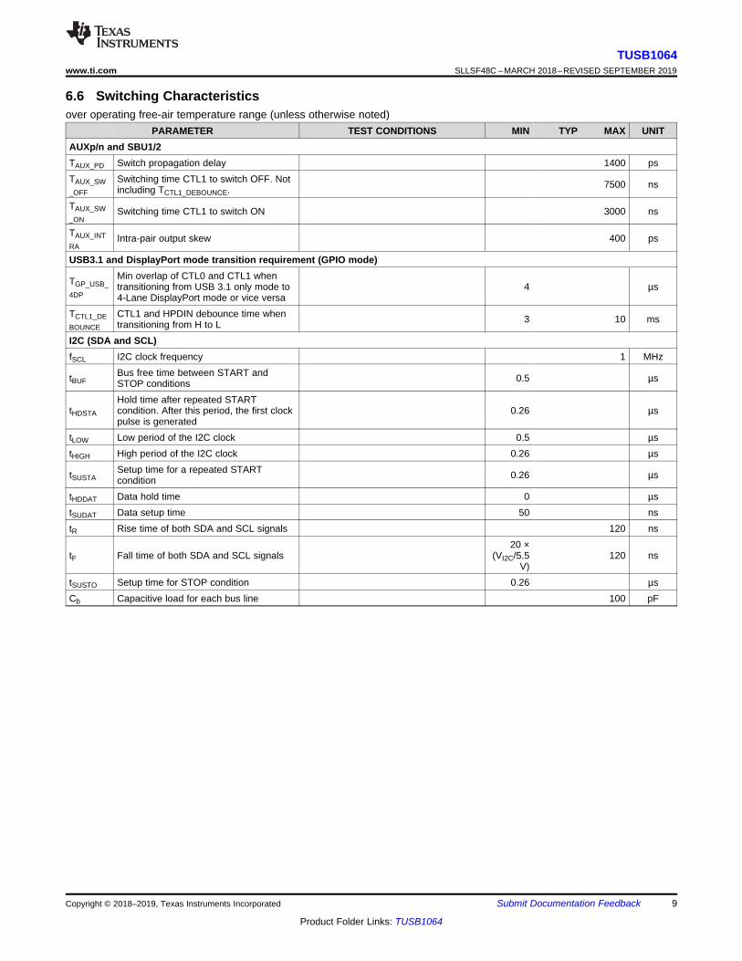
6.6 Switching Characteristicsover operating free-air temperature range (unless otherwise noted)
PARAMETER TEST CONDITIONS MIN TYP MAX UNITAUXp/n and SBU1/2TAUX_PD Switch propagation delay 1400 psTAUX_SW_OFF
Switching time CTL1 to switch OFF. Notincluding TCTL1_DEBOUNCE. 7500 ns
TAUX_SW_ON
Switching time CTL1 to switch ON 3000 ns
TAUX_INTRA
Intra-pair output skew 400 ps
USB3.1 and DisplayPort mode transition requirement (GPIO mode)
TGP_USB_4DP
Min overlap of CTL0 and CTL1 whentransitioning from USB 3.1 only mode to4-Lane DisplayPort mode or vice versa
4 µs
TCTL1_DEBOUNCE
CTL1 and HPDIN debounce time whentransitioning from H to L 3 10 ms
I2C (SDA and SCL)fSCL I2C clock frequency 1 MHz
tBUFBus free time between START andSTOP conditions 0.5 µs
tHDSTA
Hold time after repeated STARTcondition. After this period, the first clockpulse is generated
0.26 µs
tLOW Low period of the I2C clock 0.5 µstHIGH High period of the I2C clock 0.26 µs
tSUSTASetup time for a repeated STARTcondition 0.26 µs
tHDDAT Data hold time 0 µstSUDAT Data setup time 50 nstR Rise time of both SDA and SCL signals 120 ns
tF Fall time of both SDA and SCL signals20 ×
(VI2C/5.5V)
120 ns
tSUSTO Setup time for STOP condition 0.26 µsCb Capacitive load for each bus line 100 pF
10
TUSB1064SLLSF48C –MARCH 2018–REVISED SEPTEMBER 2019 www.ti.com
Product Folder Links: TUSB1064
Submit Documentation Feedback Copyright © 2018–2019, Texas Instruments Incorporated
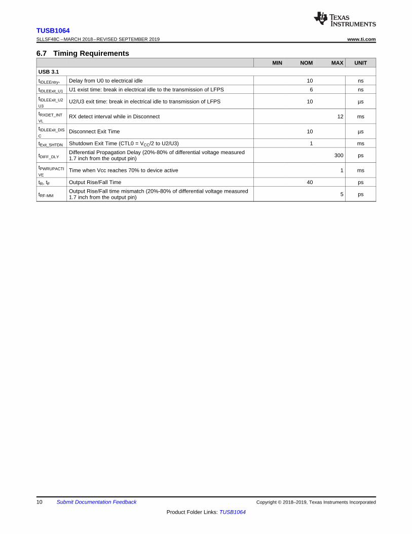
6.7 Timing RequirementsMIN NOM MAX UNIT
USB 3.1tIDLEEntry, Delay from U0 to electrical idle 10 nstIDLEExit_U1 U1 exist time: break in electrical idle to the transmission of LFPS 6 nstIDLEExit_U2U3
U2/U3 exit time: break in electrical idle to transmission of LFPS 10 µs
tRXDET_INTVL
RX detect interval while in Disconnect 12 ms
tIDLEExit_DISC
Disconnect Exit Time 10 µs
tExit_SHTDN Shutdown Exit Time (CTL0 = VCC/2 to U2/U3) 1 ms
tDIFF_DLYDifferential Propagation Delay (20%-80% of differential voltage measured1.7 inch from the output pin) 300 ps
tPWRUPACTIVE
Time when Vcc reaches 70% to device active 1 ms
tR, tF Output Rise/Fall Time 40 ps
tRF-MMOutput Rise/Fall time mismatch (20%-80% of differential voltage measured1.7 inch from the output pin) 5 ps
Differential Input Voltage (mV)
Diffe
rential O
utp
ut V
oltage (
mV
)
0 500 1000 1500 20000
200
400
600
800
1000
1200
1400
D002
EQ0EQ2EQ4EQ6EQ8EQ10EQ12EQ15
Differential Input Voltage (mV)
Diffe
rential O
utp
ut V
oltage (
mV
)
0 500 1000 1500 20000
200
400
600
800
1000
1200
D001
EQ0EQ2EQ4EQ6EQ8EQ10EQ12EQ15
0
200
400
600
800
1000
1200
1400
1600
0 200 400 600 800 1000 1200 1400 1600 1800 2000
Dif
fere
nti
al O
utp
ut
Vo
lta
ge
(m
V)
Differential Input Voltage (mV)
EQ0 EQ2 EQ4
EQ6 EQ7 EQ10
EQ12 EQ15
11
TUSB1064www.ti.com SLLSF48C –MARCH 2018–REVISED SEPTEMBER 2019
Product Folder Links: TUSB1064
Submit Documentation FeedbackCopyright © 2018–2019, Texas Instruments Incorporated
6.8 Typical Characteristics
Figure 1. DisplayPort EQ Settings Curves Figure 2. USB RX (DFP) EQ Settings Curves
Figure 3. USB TX (UFP) EQ Settings Curves Figure 4. DisplayPort Linearity Curves at 4.05 GHz
Figure 5. USB TX (DFP) Linearity Curves at 5 GHz Figure 6. USB RX (UFP) Linearity Curves at 5 GHz
Time (20.57 ps/Div)
Ou
tpu
t V
olt
ag
e (
15
0 m
V/D
iv)
Time (16.67 ps/Div)
Ou
tpu
t V
olt
ag
e (
20
0 m
V/D
iv)
-30
-25
-20
-15
-10
-5
0
0.01 0.1 1 10
SD
D1
1 (
dB
)
Frequency (GHz)
RX1 TX1 SSTX
-30
-25
-20
-15
-10
-5
0
0.01 0.1 1 10
SD
D1
1 (
dB
)
Frequency (GHz)
DP0 DP3 SSRX TX1
12
TUSB1064SLLSF48C –MARCH 2018–REVISED SEPTEMBER 2019 www.ti.com
Product Folder Links: TUSB1064
Submit Documentation Feedback Copyright © 2018–2019, Texas Instruments Incorporated
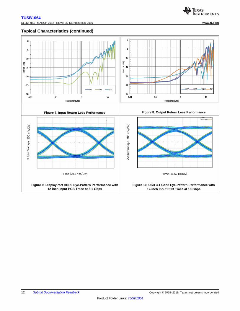
Typical Characteristics (continued)
Figure 7. Input Return Loss Performance Figure 8. Output Return Loss Performance
Figure 9. DisplayPort HBR3 Eye-Pattern Performance with12-inch Input PCB Trace at 8.1 Gbps
Figure 10. USB 3.1 Gen2 Eye-Pattern Performance with12-inch Input PCB Trace at 10 Gbps

IN
OUT
TDIFF_DLY TDIFF_DLY
CTL0 pin
CTL1 pin
4us
(min)
tBUF
tHDSTA
tRtLOW
tHDDAT
tHIGH
tF
tSUDAT tSUSTA
tHDSTA
tSUSTO
P S S P
SDA
SCL
30%
70%
30%
70%
13
TUSB1064www.ti.com SLLSF48C –MARCH 2018–REVISED SEPTEMBER 2019
Product Folder Links: TUSB1064
Submit Documentation FeedbackCopyright © 2018–2019, Texas Instruments Incorporated
7 Parameter Measurement Information
Figure 11. I2C Timing Diagram Definitions
Figure 12. USB3.1 to 4-Lane DisplayPort in GPIO Mode
Figure 13. Propagation Delay
CTL1
VOUT
50%
90%
50%
10%
TAUX_SW_ON TAUX_SW_OFF + TCTL1_DEBOUNCE
tr tf
20%
80%
TIDLEExit TIDLEEntry
IN+
IN-
Vcm
OUT+
OUT-
Vcm
VRX-LFPS-DET-DIFF-PP
14
TUSB1064SLLSF48C –MARCH 2018–REVISED SEPTEMBER 2019 www.ti.com
Product Folder Links: TUSB1064
Submit Documentation Feedback Copyright © 2018–2019, Texas Instruments Incorporated
Parameter Measurement Information (continued)
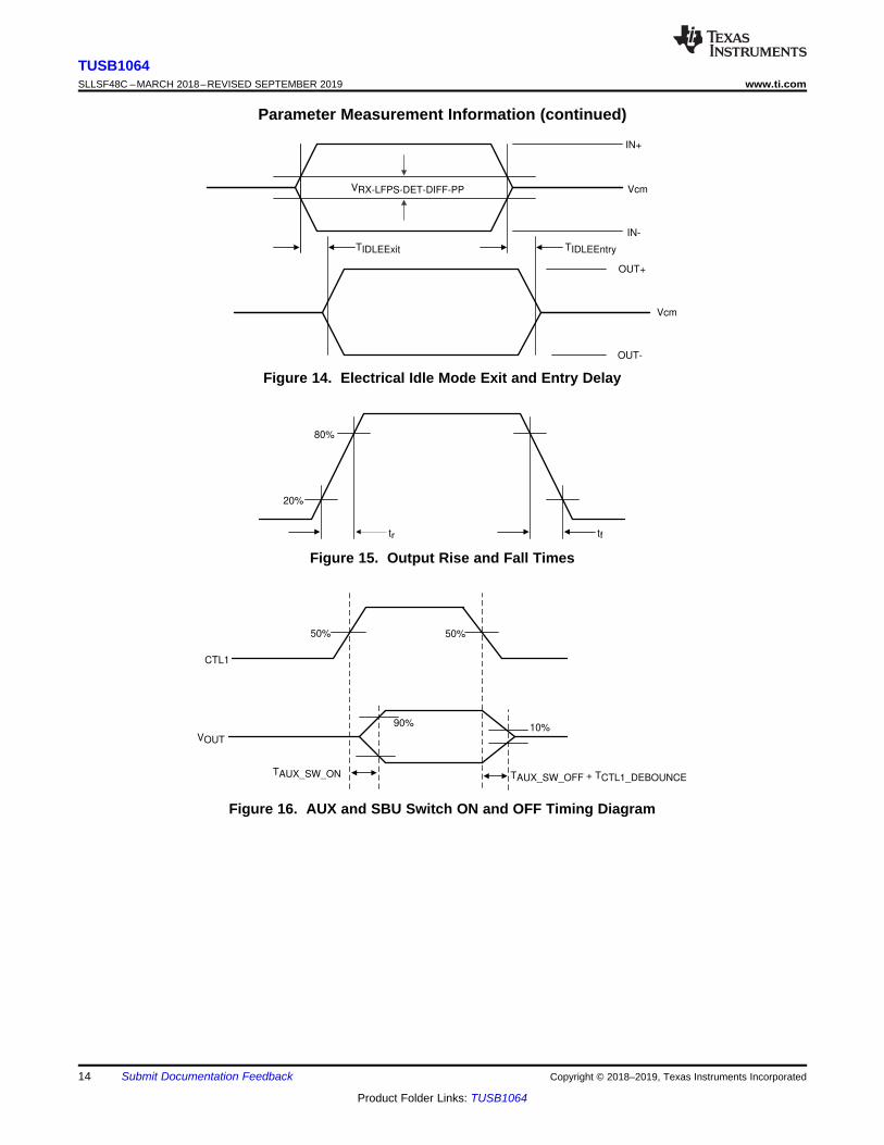
Figure 14. Electrical Idle Mode Exit and Entry Delay
Figure 15. Output Rise and Fall Times
Figure 16. AUX and SBU Switch ON and OFF Timing Diagram
15
TUSB1064www.ti.com SLLSF48C –MARCH 2018–REVISED SEPTEMBER 2019
Product Folder Links: TUSB1064
Submit Documentation FeedbackCopyright © 2018–2019, Texas Instruments Incorporated
8 Detailed Description
8.1 OverviewThe TUSB1064 is a VESA USB Type-C Alt Mode redriving switch supporting data rates up to 8.1 Gbps forupstream facing port. This device uses 5th generation USB redriver technology. The device is used for UFP pinassignments C and D from the VESA DisplayPort Alt Mode on USB Type-C Standard.
The TUSB1064 provides several levels of receive equalization to compensate for cable and board trace losswhich if not equalized causes inter-symbol interference (ISI) when USB 3.1 Gen 2 or DisplayPort 1.4 signalstravel across a PCB or cable. This device requires a 3.3-V power supply. It comes in a commercial temperaturerange and industrial temperature range.
For a sink application, the TUSB1064 enables the system to pass both transmitter compliance and receiver jittertolerance tests for USB 3.1 Gen 2 and DisplayPort version 1.4 HBR3. The re-driver recovers incoming data byapplying equalization that compensates for channel loss, and drives out signals with a high differential voltage.Each channel has a receiver equalizer with selectable gain settings. The equalization should be set based on theamount of insertion loss in the channels connected to the TUSB1064. Independent equalization control for eachchannel can be set using EQ[1:0], SSEQ[1:0], and DPEQ[1:0] pins.
The TUSB1064 advanced state machine makes it transparent to hosts and devices. After power up, theTUSB1064 periodically performs receiver detection on the TX pairs. If it detects a USB 3.1 receiver, the RXtermination is enabled, and the TTUSB1064 is ready to re-drive.
The device ultra-low-power architecture operates at a 3.3-V power supply and achieves Enhanced performance.The automatic LFPS De-Emphasis control further enables the system to be USB3.1 compliant.
DP0p
DP0n
DP3p
DP3n
I2C_EN
DPEQ[1:0]/A1
SSEQ[1:0]/A0
SBU2
SBU1
CTL0/SDA
FLIP/SCL
VCC
AUXn
AUXp
SSTXp
SSRXn
SSRXp
SSTXn
RX1p
TX2p
TX1p
RX1n
TX2n
TX1n
RX2p
RX2n
EQ[1:0]
EN
Driver
EQ Driver
EQ
EQ
Driver
EQ
EQ
Te
rm
De
tect
Te
rm
Te
rmT
erm
Te
rm
Te
rmT
erm
Te
rm
M
U
X
VREG
MUXMUX
Driver
FSM, Control Logic and
Registers
DPEQ_SEL
SSEQ_SEL
SSEQ_SEL
EQ_SEL
DPEQ_SEL
DPEQ_SEL
DP1p
DP1n
DP2p
DP2n
CTL1
AU
X
RX
I2C
Slave
Copyright © 2017, Texas Instruments Incorporated
DPEQ_SEL
EQ_SEL
DPEQ_SEL
EQ_SEL
De
tect
De
tect
Te
rm
Driver
Te
rm
Driver
Te
rm
Driver
Te
rm
HPDIN
16
TUSB1064SLLSF48C –MARCH 2018–REVISED SEPTEMBER 2019 www.ti.com
Product Folder Links: TUSB1064
Submit Documentation Feedback Copyright © 2018–2019, Texas Instruments Incorporated
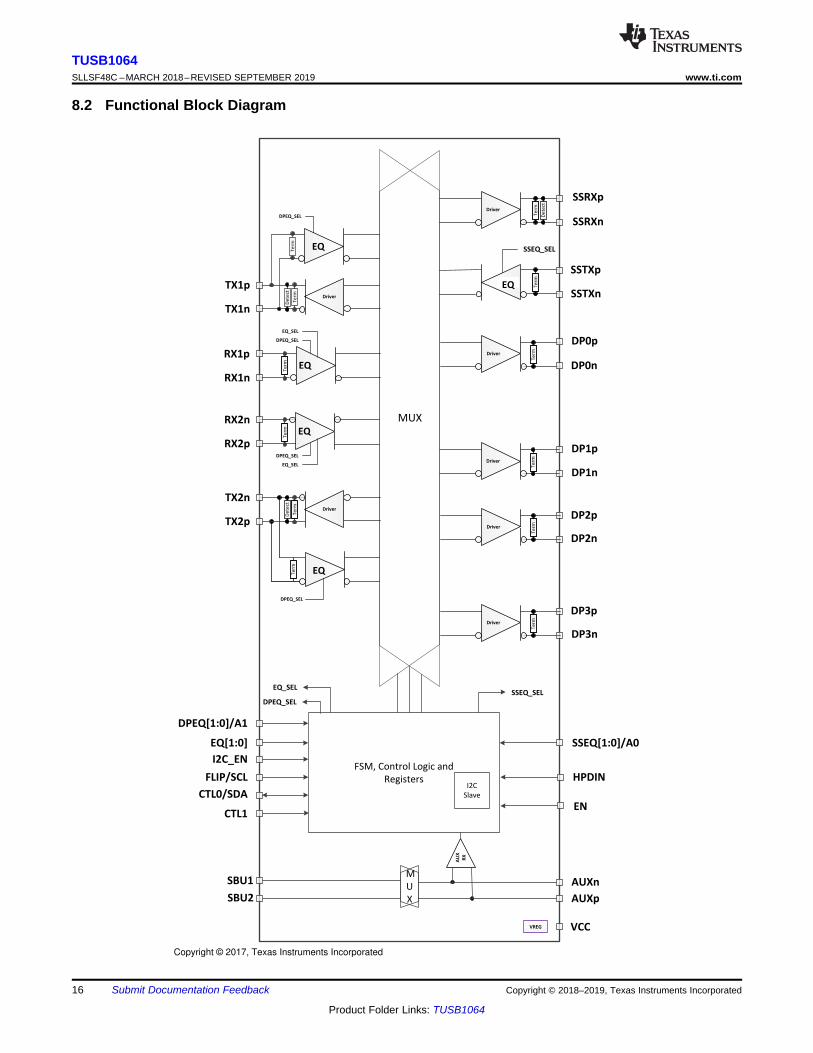
8.2 Functional Block Diagram
17
TUSB1064www.ti.com SLLSF48C –MARCH 2018–REVISED SEPTEMBER 2019
Product Folder Links: TUSB1064
Submit Documentation FeedbackCopyright © 2018–2019, Texas Instruments Incorporated
8.3 Feature Description
8.3.1 USB 3.1The TUSB1064 supports USB 3.1 Gen 2 datarates up to 10 Gbps. The TUSB1064 supports all the USB definedpower states (U0, U1, U2, and U3). Because the TUSB1064 is a linear redriver, it can’t decode USB3.1 physicallayer traffic. The TUSB1064 monitors the actual physical layer conditions like receiver termination, electrical idle,LFPS, and SuperSpeed signaling rate to determine the USB power state of the USB 3.1 interface.
The TUSB1064 features an intelligent low frequency periodic signaling (LFPS) detector. The LFPS detectorautomatically senses the low frequency signals and disables receiver equalization functionality. When notreceiving LFPS, the TUSB1064 enables receiver equalization based on the EQ[1:0] and SSEQ[1:0] pins orvalues programmed into EQ1_SEL, EQ2_SEL, and SSEQ_SEL registers.
8.3.2 DisplayPortThe TUSB1064 supports up to 4 DisplayPort lanes at datarates up to 8.1Gbps (HBR3). The TUSB1064, whenconfigured in DisplayPort mode, monitors the native AUX traffic as it traverses between DisplayPort source andDisplayPort sink. For the purposes of reducing power, the TUSB1064 manages the number of active DisplayPortlanes based on the content of the AUX transactions. The TUSB1064 snoops native AUX writes to DisplayPortsink’s DPCD registers 0x00101 (LANE_COUNT_SET) and 0x00600 (SET_POWER_STATE).TUSB1064disables/enables lanes based on value written to LANE_COUNT_SET. The TUSB1064 disables alllanes when SET_POWER_STATE is in the D3. Otherwise, active lanes are based on value ofLANE_COUNT_SET.
DisplayPort AUX snooping is enabled by default but can be disabled by changing the AUX_SNOOP_DISABLEregister. Once AUX snoop is disabled, management of TUSB1064 DisplayPort lanes are controlled throughvarious configuration registers.
NOTEAUX snooping feature is only supported when TUSB1064 is configured for I2C mode.When TUSB1064 is configured for GPIO mode, the AUX snoop feature is disabled and allfour DP lanes are enabled if HPDIN is asserted high.
When TUSB1064’s AUX snoop feature is enabled, the syncs defined by the DisplayPortstandard must be received in order for AUX snoop feature to function properly. AUX writesto panel’s DPCD address 0x00600 and 0x00101 should result in SET_POWER_STATEand LANE_COUNT_SET fields at TUSB1064’s offset 0x12 to get set to the appropriatevalue. If these fields do not get set correctly, then incoming AUX may not be compliant. Ifthis is the case, then it is best to disable AUX snoop by setting theAUX_SNOOP_DISABLE field at offset 0x13.
8.3.3 4-level InputsThe TUSB1064 has (I2C_EN, EQ[1:0], DPEQ[1:0], and SSEQ[1:0]) 4-level inputs pins that are used to controlthe equalization gain and place TUSB1064 into different modes of operation. These 4-level inputs utilize aresistor divider to help set the 4 valid levels and provide a wider range of control settings. There is an internal 35kΩ pull-up and a 95 kΩ pull-down. These resistors, together with the external resistor connection combine toachieve the desired voltage level.
Table 1. 4-Level Control Pin SettingsLEVEL SETTINGS
0 Option 1: Tie 1 KΩ 5% to GND.Option 2: Tie directly to GND.
R Tie 20 KΩ 5% to GND.F Float (leave pin open)
1 Option 1: Tie 1 KΩ 5%to VCC.Option 2: Tie directly to VCC.
18
TUSB1064SLLSF48C –MARCH 2018–REVISED SEPTEMBER 2019 www.ti.com
Product Folder Links: TUSB1064
Submit Documentation Feedback Copyright © 2018–2019, Texas Instruments Incorporated
NOTEAll four-level inputs are latched on rising edge of internal reset. After tcfg_hd, the internalpull-up and pull-down resistors will be isolated in order to save power.
8.3.4 Receiver Linear EqualizationThe purpose of receiver equalization is to compensate for channel insertion loss and the resulting inter-symbolinterference in the system before the input or after the output of the TUSB1064. The receiver overcomes theselosses by attenuating the low frequency components of the signals with respect to the high frequencycomponents. The proper gain setting should be selected to match the channel insertion loss. Two 4-level inputpins enable up to 16 possible equalization settings. USB3.1 upstream path, USB3.1 downstream path, andDisplayPort each have their own two 4-level inputs. The TUSB1064 also provides the flexibility of adjustingsettings through I2C registers.
8.4 Device Functional Modes
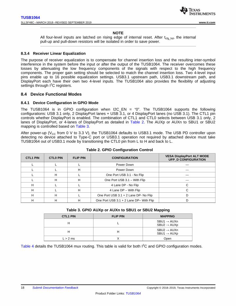
8.4.1 Device Configuration in GPIO ModeThe TUSB1064 is in GPIO configuration when I2C_EN = “0”. The TUSB1064 supports the followingconfigurations: USB 3.1 only, 2 DisplayPort lanes + USB 3.1, or 4 DisplayPort lanes (no USB 3.1). The CTL1 pincontrols whether DisplayPort is enabled. The combination of CTL1 and CTL0 selects between USB 3.1 only, 2lanes of DisplayPort, or 4-lanes of DisplayPort as detailed in Table 2. The AUXp or AUXn to SBU1 or SBU2mapping is controlled based on Table 3.
After power-up (VCC from 0 V to 3.3 V), the TUSB1064 defaults to USB3.1 mode. The USB PD controller upondetecting no device attached to Type-C port or USB3.1 operation not required by attached device must takeTUSB1064 out of USB3.1 mode by transitioning the CTL0 pin from L to H and back to L.
Table 2. GPIO Configuration Control
CTL1 PIN CTL0 PIN FLIP PIN CONFIGURATION VESA DisplayPort ALT MODEUFP_D CONFIGURATION
L L L Power Down —L L H Power Down —L H L One Port USB 3.1 - No Flip —L H H One Port USB 3.1 – With Flip —H L L 4 Lane DP - No Flip CH L H 4 Lane DP – With Flip CH H L One Port USB 3.1 + 2 Lane DP- No Flip DH H H One Port USB 3.1 + 2 Lane DP– With Flip D
Table 3. GPIO AUXp or AUXn to SBU1 or SBU2 MappingCTL1 PIN FLIP PIN MAPPING
H L SBU1 → AUXnSBU2 → AUXp
H H SBU2 → AUXnSBU1 → AUXp
L > 2 ms X Open
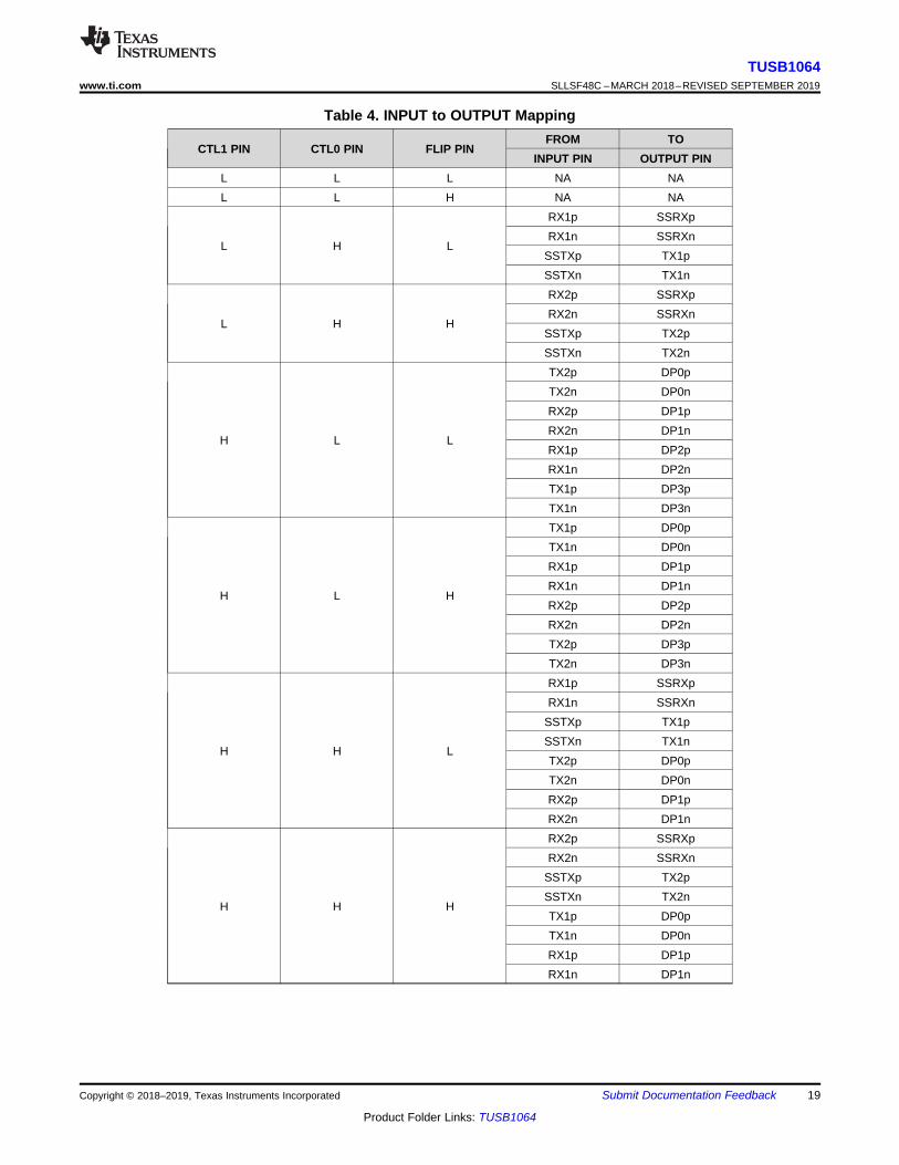
Table 4 details the TUSB1064 mux routing. This table is valid for both I2C and GPIO configuration modes.
19
TUSB1064www.ti.com SLLSF48C –MARCH 2018–REVISED SEPTEMBER 2019
Product Folder Links: TUSB1064
Submit Documentation FeedbackCopyright © 2018–2019, Texas Instruments Incorporated
Table 4. INPUT to OUTPUT Mapping
CTL1 PIN CTL0 PIN FLIP PINFROM TO
INPUT PIN OUTPUT PINL L L NA NAL L H NA NA
L H L
RX1p SSRXpRX1n SSRXn
SSTXp TX1pSSTXn TX1n
L H H
RX2p SSRXpRX2n SSRXn
SSTXp TX2pSSTXn TX2n
H L L
TX2p DP0pTX2n DP0nRX2p DP1pRX2n DP1nRX1p DP2pRX1n DP2nTX1p DP3pTX1n DP3n
H L H
TX1p DP0pTX1n DP0nRX1p DP1pRX1n DP1nRX2p DP2pRX2n DP2nTX2p DP3pTX2n DP3n
H H L
RX1p SSRXpRX1n SSRXn
SSTXp TX1pSSTXn TX1nTX2p DP0pTX2n DP0nRX2p DP1pRX2n DP1n
H H H
RX2p SSRXpRX2n SSRXn
SSTXp TX2pSSTXn TX2nTX1p DP0pTX1n DP0nRX1p DP1pRX1n DP1n
20
TUSB1064SLLSF48C –MARCH 2018–REVISED SEPTEMBER 2019 www.ti.com
Product Folder Links: TUSB1064
Submit Documentation Feedback Copyright © 2018–2019, Texas Instruments Incorporated
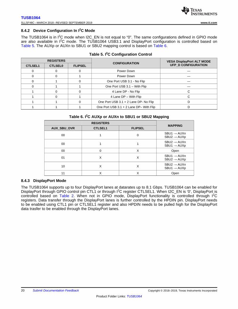
8.4.2 Device Configuration In I2C ModeThe TUSB1064 is in I2C mode when I2C_EN is not equal to “0”. The same configurations defined in GPIO modeare also available in I2C mode. The TUSB1064 USB3.1 and DisplayPort configuration is controlled based onTable 5. The AUXp or AUXn to SBU1 or SBU2 mapping control is based on Table 6.
Table 5. I2C Configuration ControlREGISTERS
CONFIGURATION VESA DisplayPort ALT MODEUFP_D CONFIGURATIONCTLSEL1 CTLSEL0 FLIPSEL
0 0 0 Power Down —0 0 1 Power Down —0 1 0 One Port USB 3.1 - No Flip —0 1 1 One Port USB 3.1 – With Flip —1 0 0 4 Lane DP - No Flip C1 0 1 4 Lane DP – With Flip C1 1 0 One Port USB 3.1 + 2 Lane DP- No Flip D1 1 1 One Port USB 3.1 + 2 Lane DP– With Flip D
Table 6. I2C AUXp or AUXn to SBU1 or SBU2 MappingREGISTERS
MAPPINGAUX_SBU_OVR CTLSEL1 FLIPSEL
00 1 0 SBU1 → AUXnSBU2 → AUXp
00 1 1 SBU2 → AUXnSBU1 → AUXp
00 0 X Open
01 X X SBU1 → AUXnSBU2 → AUXp
10 X X SBU2 → AUXnSBU1 → AUXp
11 X X Open
8.4.3 DisplayPort ModeThe TUSB1064 supports up to four DisplayPort lanes at datarates up to 8.1 Gbps. TUSB1064 can be enabled forDisplayPort through GPIO control pin CTL1 or through I2C register CTLSEL1. When I2C_EN is ‘0’, DisplayPort iscontrolled based on Table 2. When not in GPIO mode, DisplayPort functionality is controlled through I2Cregisters. Data transfer through the DisplayPort lanes is further controlled by the HPDIN pin. DisplayPort needsto be enabled using CTL1 pin or CTLSEL1 register and also HPDIN needs to be pulled high for the DisplayPortdata trasfer to be enabled through the DisplayPort lanes.
21
TUSB1064www.ti.com SLLSF48C –MARCH 2018–REVISED SEPTEMBER 2019
Product Folder Links: TUSB1064
Submit Documentation FeedbackCopyright © 2018–2019, Texas Instruments Incorporated
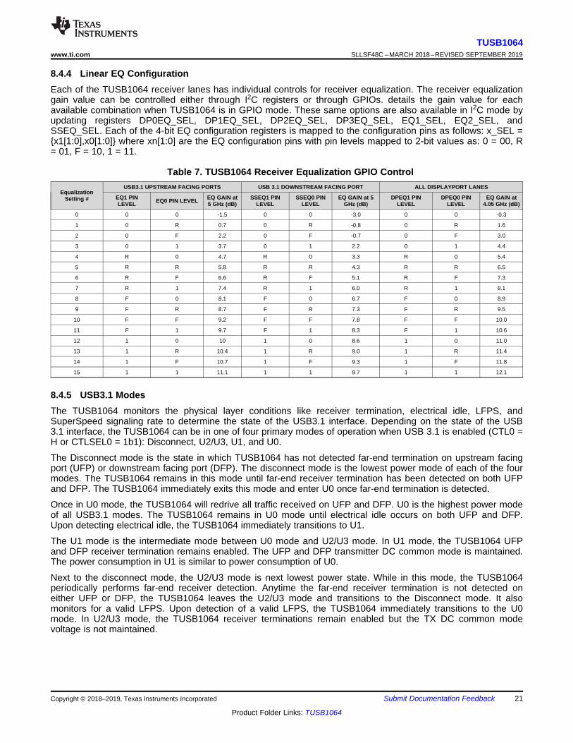
8.4.4 Linear EQ ConfigurationEach of the TUSB1064 receiver lanes has individual controls for receiver equalization. The receiver equalizationgain value can be controlled either through I2C registers or through GPIOs. details the gain value for eachavailable combination when TUSB1064 is in GPIO mode. These same options are also available in I2C mode byupdating registers DP0EQ_SEL, DP1EQ_SEL, DP2EQ_SEL, DP3EQ_SEL, EQ1_SEL, EQ2_SEL, andSSEQ_SEL. Each of the 4-bit EQ configuration registers is mapped to the configuration pins as follows: x_SEL =x1[1:0],x0[1:0] where xn[1:0] are the EQ configuration pins with pin levels mapped to 2-bit values as: 0 = 00, R= 01, F = 10, 1 = 11.
Table 7. TUSB1064 Receiver Equalization GPIO Control
EqualizationSetting #
USB3.1 UPSTREAM FACING PORTS USB 3.1 DOWNSTREAM FACING PORT ALL DISPLAYPORT LANES
EQ1 PINLEVEL EQ0 PIN LEVEL EQ GAIN at
5 GHz (dB)SSEQ1 PIN
LEVELSSEQ0 PIN
LEVELEQ GAIN at 5
GHz (dB)DPEQ1 PIN
LEVELDPEQ0 PIN
LEVELEQ GAIN at
4.05 GHz (dB)
0 0 0 -1.5 0 0 -3.0 0 0 -0.3
1 0 R 0.7 0 R -0.8 0 R 1.6
2 0 F 2.2 0 F -0.7 0 F 3.0
3 0 1 3.7 0 1 2.2 0 1 4.4
4 R 0 4.7 R 0 3.3 R 0 5.4
5 R R 5.8 R R 4.3 R R 6.5
6 R F 6.6 R F 5.1 R F 7.3
7 R 1 7.4 R 1 6.0 R 1 8.1
8 F 0 8.1 F 0 6.7 F 0 8.9
9 F R 8.7 F R 7.3 F R 9.5
10 F F 9.2 F F 7.8 F F 10.0
11 F 1 9.7 F 1 8.3 F 1 10.6
12 1 0 10 1 0 8.6 1 0 11.0
13 1 R 10.4 1 R 9.0 1 R 11.4
14 1 F 10.7 1 F 9.3 1 F 11.8
15 1 1 11.1 1 1 9.7 1 1 12.1
8.4.5 USB3.1 ModesThe TUSB1064 monitors the physical layer conditions like receiver termination, electrical idle, LFPS, andSuperSpeed signaling rate to determine the state of the USB3.1 interface. Depending on the state of the USB3.1 interface, the TUSB1064 can be in one of four primary modes of operation when USB 3.1 is enabled (CTL0 =H or CTLSEL0 = 1b1): Disconnect, U2/U3, U1, and U0.
The Disconnect mode is the state in which TUSB1064 has not detected far-end termination on upstream facingport (UFP) or downstream facing port (DFP). The disconnect mode is the lowest power mode of each of the fourmodes. The TUSB1064 remains in this mode until far-end receiver termination has been detected on both UFPand DFP. The TUSB1064 immediately exits this mode and enter U0 once far-end termination is detected.
Once in U0 mode, the TUSB1064 will redrive all traffic received on UFP and DFP. U0 is the highest power modeof all USB3.1 modes. The TUSB1064 remains in U0 mode until electrical idle occurs on both UFP and DFP.Upon detecting electrical idle, the TUSB1064 immediately transitions to U1.
The U1 mode is the intermediate mode between U0 mode and U2/U3 mode. In U1 mode, the TUSB1064 UFPand DFP receiver termination remains enabled. The UFP and DFP transmitter DC common mode is maintained.The power consumption in U1 is similar to power consumption of U0.
Next to the disconnect mode, the U2/U3 mode is next lowest power state. While in this mode, the TUSB1064periodically performs far-end receiver detection. Anytime the far-end receiver termination is not detected oneither UFP or DFP, the TUSB1064 leaves the U2/U3 mode and transitions to the Disconnect mode. It alsomonitors for a valid LFPS. Upon detection of a valid LFPS, the TUSB1064 immediately transitions to the U0mode. In U2/U3 mode, the TUSB1064 receiver terminations remain enabled but the TX DC common modevoltage is not maintained.
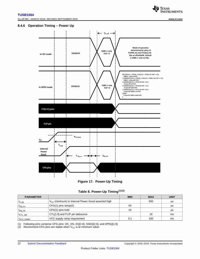
Td_pg
VCC
Internal
Power
GoodT Cfg_su TCfg_hd
DISABLEDUSB3.1- only
FLIP = 0
If (( CTL[1:0 ] == 2'b 00 | CTL[1:0 ] == 2'b01 ) & FLIP == 0 )
USB3.1- only no FLIP;
ELSEIF ((CTL[1:0 ] == 2'b 00 | CTL[1:0 ] == 2'b01 ) & FLIP == 1 )
USB3.1- only with FLIP ;
ELSEIF (CTL[1:0 ] == 2'b 10 & FLIP == 0 )
4-Lane DP no FLIP;
ELSEIF (CTL[1:0 ] == 2'b 10 & FLIP == 1 )
4-Lane DP with FLIP;
ELSEIF (CTL[1:0 ] == 2'b 11 & FLIP == 0 )
2-Lane DP USB3.1 no FLIP;
ELSE
2-Lane DP USB3.1 with FLIP ;
;
CTL[1:0 ] pins
FLIP pin
CFG pins
In GPIO mode
DISABLEDUSB3.1- only
FLIP = 0In I2C mode
Mode of operation
determined by value of
FLIPSEL bit and CTLSEL[1:0]
bits at offset0x0A. Default
is USB3.1- only no Flip.
Tctl_db
VCC (min)
22
TUSB1064SLLSF48C –MARCH 2018–REVISED SEPTEMBER 2019 www.ti.com
Product Folder Links: TUSB1064
Submit Documentation Feedback Copyright © 2018–2019, Texas Instruments Incorporated
(1) Following pins comprise CFG pins: I2C_EN, EQ[1:0], SSEQ[1:0], and DPEQ[1:0].(2) Recommend CFG pins are stable when VCC is at minimum value.
8.4.6 Operation Timing – Power Up
Figure 17. Power-Up Timing
Table 8. Power-Up Timing (1) (2)
PARAMETER MIN MAX UNITtd_pg VCC (minimum) to Internal Power Good asserted high 500 µstcfg_su CFG(1) pins setup(2) 50 µstcfg_hd CFG(1) pins hold 10 µstCTL_DB CTL[1:0] and FLIP pin debounce 16 mstVCC_RAMP VCC supply ramp requirement 0.1 100 ms
23
TUSB1064www.ti.com SLLSF48C –MARCH 2018–REVISED SEPTEMBER 2019
Product Folder Links: TUSB1064
Submit Documentation FeedbackCopyright © 2018–2019, Texas Instruments Incorporated
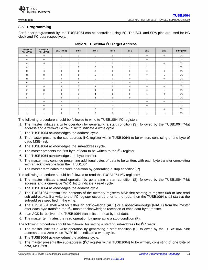
8.5 ProgrammingFor further programmability, the TUSB1064 can be controlled using I2C. The SCL and SDA pins are used for I2Cclock and I2C data respectively.
Table 9. TUSB1064 I2C Target AddressDPEQ0/A1PIN LEVEL
SSEQ0/A0PIN LEVEL Bit 7 (MSB) Bit 6 Bit 5 Bit 4 Bit 3 Bit 2 Bit 1 Bit 0 (W/R)
0 0 1 0 0 0 1 0 0 0/1
0 R 1 0 0 0 1 0 1 0/1
0 F 1 0 0 0 1 1 0 0/1
0 1 1 0 0 0 1 1 1 0/1
R 0 0 1 0 0 0 0 0 0/1
R R 0 1 0 0 0 0 1 0/1
R F 0 1 0 0 0 1 0 0/1
R 1 0 1 0 0 0 1 1 0/1
F 0 0 0 1 0 0 0 0 0/1
F R 0 0 1 0 0 0 1 0/1
F F 0 0 1 0 0 1 0 0/1
F 1 0 0 1 0 0 1 1 0/1
1 0 0 0 0 1 1 0 0 0/1
1 R 0 0 0 1 1 0 1 0/1
1 F 0 0 0 1 1 1 0 0/1
1 1 0 0 0 1 1 1 1 0/1
The following procedure should be followed to write to TUSB1064 I2C registers:1. The master initiates a write operation by generating a start condition (S), followed by the TUSB1064 7-bit
address and a zero-value “W/R” bit to indicate a write cycle.2. The TUSB1064 acknowledges the address cycle.3. The master presents the sub-address (I2C register within TUSB1064) to be written, consisting of one byte of
data, MSB-first.4. The TUSB1064 acknowledges the sub-address cycle.5. The master presents the first byte of data to be written to the I2C register.6. The TUSB1064 acknowledges the byte transfer.7. The master may continue presenting additional bytes of data to be written, with each byte transfer completing
with an acknowledge from the TUSB1064.8. The master terminates the write operation by generating a stop condition (P).
The following procedure should be followed to read the TUSB1064 I2C registers:1. The master initiates a read operation by generating a start condition (S), followed by the TUSB1064 7-bit
address and a one-value “W/R” bit to indicate a read cycle.2. The TUSB1064 acknowledges the address cycle.3. The TUSB1064 transmit the contents of the memory registers MSB-first starting at register 00h or last read
sub-address+1. If a write to the I2C register occurred prior to the read, then the TUSB1064 shall start at thesub-address specified in the write.
4. The TUSB1064 shall wait for either an acknowledge (ACK) or a not-acknowledge (NACK) from the masterafter each byte transfer; the I2C master acknowledges reception of each data byte transfer.
5. If an ACK is received, the TUSB1064 transmits the next byte of data.6. The master terminates the read operation by generating a stop condition (P).
The following procedure should be followed for setting a starting sub-address for I2C reads:1. The master initiates a write operation by generating a start condition (S), followed by the TUSB1064 7-bit
address and a zero-value “W/R” bit to indicate a write cycle.2. The TUSB1064 acknowledges the address cycle.3. The master presents the sub-address (I2C register within TUSB1064) to be written, consisting of one byte of
data, MSB-first.
24
TUSB1064SLLSF48C –MARCH 2018–REVISED SEPTEMBER 2019 www.ti.com
Product Folder Links: TUSB1064
Submit Documentation Feedback Copyright © 2018–2019, Texas Instruments Incorporated
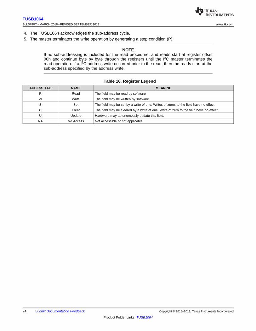
4. The TUSB1064 acknowledges the sub-address cycle.5. The master terminates the write operation by generating a stop condition (P).
NOTEIf no sub-addressing is included for the read procedure, and reads start at register offset00h and continue byte by byte through the registers until the I2C master terminates theread operation. If a I2C address write occurred prior to the read, then the reads start at thesub-address specified by the address write.
Table 10. Register LegendACCESS TAG NAME MEANING
R Read The field may be read by softwareW Write The field may be written by softwareS Set The field may be set by a write of one. Writes of zeros to the field have no effect.C Clear The field may be cleared by a write of one. Write of zero to the field have no effect.U Update Hardware may autonomously update this field.
NA No Access Not accessible or not applicable
25
TUSB1064www.ti.com SLLSF48C –MARCH 2018–REVISED SEPTEMBER 2019
Product Folder Links: TUSB1064
Submit Documentation FeedbackCopyright © 2018–2019, Texas Instruments Incorporated
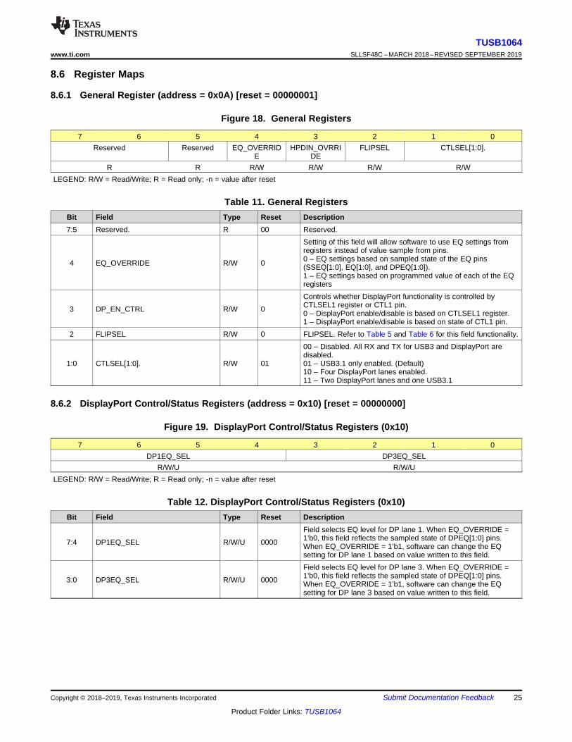
8.6 Register Maps
8.6.1 General Register (address = 0x0A) [reset = 00000001]
Figure 18. General Registers
7 6 5 4 3 2 1 0Reserved Reserved EQ_OVERRID
EHPDIN_OVRRI
DEFLIPSEL CTLSEL[1:0].
R R R/W R/W R/W R/WLEGEND: R/W = Read/Write; R = Read only; -n = value after reset
Table 11. General RegistersBit Field Type Reset Description7:5 Reserved. R 00 Reserved.
4 EQ_OVERRIDE R/W 0
Setting of this field will allow software to use EQ settings fromregisters instead of value sample from pins.0 – EQ settings based on sampled state of the EQ pins(SSEQ[1:0], EQ[1:0], and DPEQ[1:0]).1 – EQ settings based on programmed value of each of the EQregisters
3 DP_EN_CTRL R/W 0
Controls whether DisplayPort functionality is controlled byCTLSEL1 register or CTL1 pin.0 – DisplayPort enable/disable is based on CTLSEL1 register.1 – DisplayPort enable/disable is based on state of CTL1 pin.
2 FLIPSEL R/W 0 FLIPSEL. Refer to Table 5 and Table 6 for this field functionality.
1:0 CTLSEL[1:0]. R/W 01
00 – Disabled. All RX and TX for USB3 and DisplayPort aredisabled.01 – USB3.1 only enabled. (Default)10 – Four DisplayPort lanes enabled.11 – Two DisplayPort lanes and one USB3.1
8.6.2 DisplayPort Control/Status Registers (address = 0x10) [reset = 00000000]
Figure 19. DisplayPort Control/Status Registers (0x10)
7 6 5 4 3 2 1 0DP1EQ_SEL DP3EQ_SEL
R/W/U R/W/ULEGEND: R/W = Read/Write; R = Read only; -n = value after reset
Table 12. DisplayPort Control/Status Registers (0x10)Bit Field Type Reset Description
7:4 DP1EQ_SEL R/W/U 0000
Field selects EQ level for DP lane 1. When EQ_OVERRIDE =1’b0, this field reflects the sampled state of DPEQ[1:0] pins.When EQ_OVERRIDE = 1’b1, software can change the EQsetting for DP lane 1 based on value written to this field.
3:0 DP3EQ_SEL R/W/U 0000
Field selects EQ level for DP lane 3. When EQ_OVERRIDE =1’b0, this field reflects the sampled state of DPEQ[1:0] pins.When EQ_OVERRIDE = 1’b1, software can change the EQsetting for DP lane 3 based on value written to this field.
26
TUSB1064SLLSF48C –MARCH 2018–REVISED SEPTEMBER 2019 www.ti.com
Product Folder Links: TUSB1064
Submit Documentation Feedback Copyright © 2018–2019, Texas Instruments Incorporated
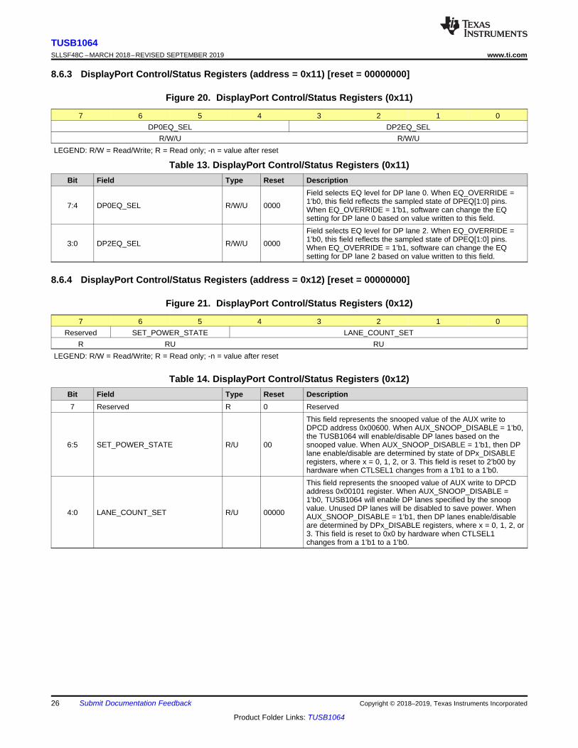
8.6.3 DisplayPort Control/Status Registers (address = 0x11) [reset = 00000000]
Figure 20. DisplayPort Control/Status Registers (0x11)
7 6 5 4 3 2 1 0DP0EQ_SEL DP2EQ_SEL
R/W/U R/W/ULEGEND: R/W = Read/Write; R = Read only; -n = value after reset
Table 13. DisplayPort Control/Status Registers (0x11)Bit Field Type Reset Description
7:4 DP0EQ_SEL R/W/U 0000
Field selects EQ level for DP lane 0. When EQ_OVERRIDE =1’b0, this field reflects the sampled state of DPEQ[1:0] pins.When EQ_OVERRIDE = 1’b1, software can change the EQsetting for DP lane 0 based on value written to this field.
3:0 DP2EQ_SEL R/W/U 0000
Field selects EQ level for DP lane 2. When EQ_OVERRIDE =1’b0, this field reflects the sampled state of DPEQ[1:0] pins.When EQ_OVERRIDE = 1’b1, software can change the EQsetting for DP lane 2 based on value written to this field.
8.6.4 DisplayPort Control/Status Registers (address = 0x12) [reset = 00000000]
Figure 21. DisplayPort Control/Status Registers (0x12)
7 6 5 4 3 2 1 0Reserved SET_POWER_STATE LANE_COUNT_SET
R RU RULEGEND: R/W = Read/Write; R = Read only; -n = value after reset
Table 14. DisplayPort Control/Status Registers (0x12)Bit Field Type Reset Description7 Reserved R 0 Reserved
6:5 SET_POWER_STATE R/U 00
This field represents the snooped value of the AUX write toDPCD address 0x00600. When AUX_SNOOP_DISABLE = 1’b0,the TUSB1064 will enable/disable DP lanes based on thesnooped value. When AUX_SNOOP_DISABLE = 1’b1, then DPlane enable/disable are determined by state of DPx_DISABLEregisters, where x = 0, 1, 2, or 3. This field is reset to 2’b00 byhardware when CTLSEL1 changes from a 1’b1 to a 1’b0.
4:0 LANE_COUNT_SET R/U 00000
This field represents the snooped value of AUX write to DPCDaddress 0x00101 register. When AUX_SNOOP_DISABLE =1’b0, TUSB1064 will enable DP lanes specified by the snoopvalue. Unused DP lanes will be disabled to save power. WhenAUX_SNOOP_DISABLE = 1’b1, then DP lanes enable/disableare determined by DPx_DISABLE registers, where x = 0, 1, 2, or3. This field is reset to 0x0 by hardware when CTLSEL1changes from a 1’b1 to a 1’b0.
27
TUSB1064www.ti.com SLLSF48C –MARCH 2018–REVISED SEPTEMBER 2019
Product Folder Links: TUSB1064
Submit Documentation FeedbackCopyright © 2018–2019, Texas Instruments Incorporated
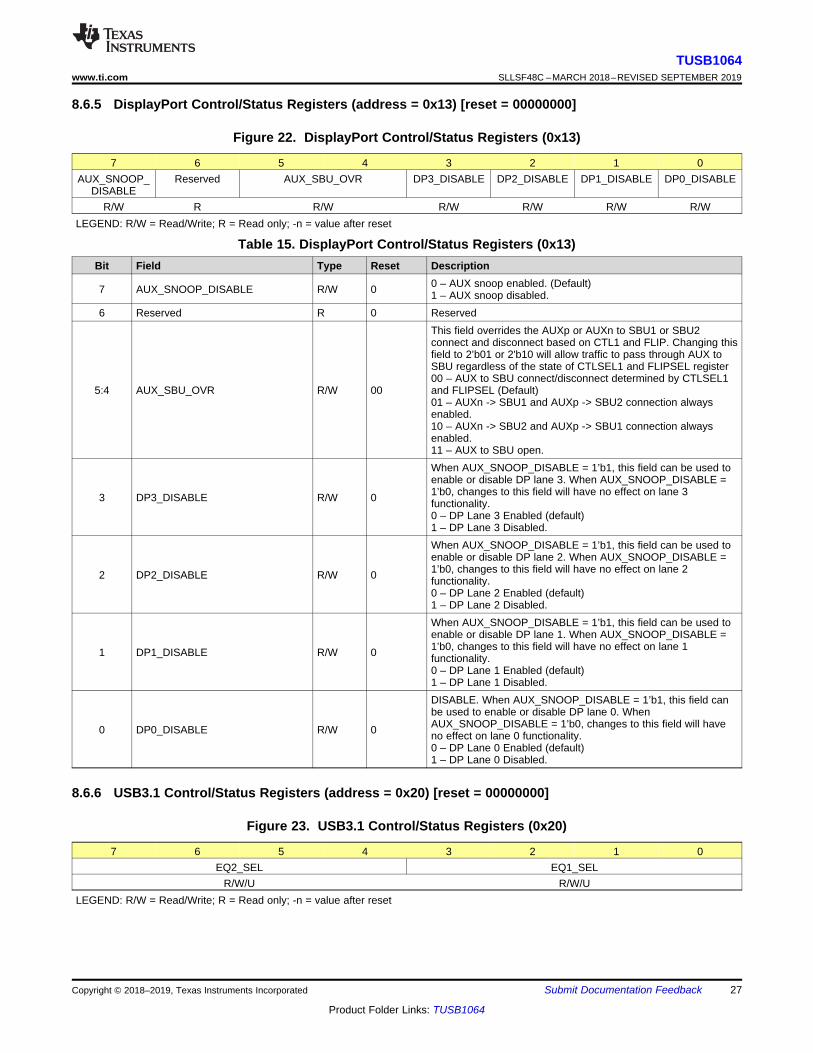
8.6.5 DisplayPort Control/Status Registers (address = 0x13) [reset = 00000000]
Figure 22. DisplayPort Control/Status Registers (0x13)
7 6 5 4 3 2 1 0AUX_SNOOP_
DISABLEReserved AUX_SBU_OVR DP3_DISABLE DP2_DISABLE DP1_DISABLE DP0_DISABLE
R/W R R/W R/W R/W R/W R/WLEGEND: R/W = Read/Write; R = Read only; -n = value after reset
Table 15. DisplayPort Control/Status Registers (0x13)Bit Field Type Reset Description
7 AUX_SNOOP_DISABLE R/W 0 0 – AUX snoop enabled. (Default)1 – AUX snoop disabled.
6 Reserved R 0 Reserved
5:4 AUX_SBU_OVR R/W 00
This field overrides the AUXp or AUXn to SBU1 or SBU2connect and disconnect based on CTL1 and FLIP. Changing thisfield to 2’b01 or 2'b10 will allow traffic to pass through AUX toSBU regardless of the state of CTLSEL1 and FLIPSEL register00 – AUX to SBU connect/disconnect determined by CTLSEL1and FLIPSEL (Default)01 – AUXn -> SBU1 and AUXp -> SBU2 connection alwaysenabled.10 – AUXn -> SBU2 and AUXp -> SBU1 connection alwaysenabled.11 – AUX to SBU open.
3 DP3_DISABLE R/W 0
When AUX_SNOOP_DISABLE = 1’b1, this field can be used toenable or disable DP lane 3. When AUX_SNOOP_DISABLE =1’b0, changes to this field will have no effect on lane 3functionality.0 – DP Lane 3 Enabled (default)1 – DP Lane 3 Disabled.
2 DP2_DISABLE R/W 0
When AUX_SNOOP_DISABLE = 1’b1, this field can be used toenable or disable DP lane 2. When AUX_SNOOP_DISABLE =1’b0, changes to this field will have no effect on lane 2functionality.0 – DP Lane 2 Enabled (default)1 – DP Lane 2 Disabled.
1 DP1_DISABLE R/W 0
When AUX_SNOOP_DISABLE = 1’b1, this field can be used toenable or disable DP lane 1. When AUX_SNOOP_DISABLE =1’b0, changes to this field will have no effect on lane 1functionality.0 – DP Lane 1 Enabled (default)1 – DP Lane 1 Disabled.
0 DP0_DISABLE R/W 0
DISABLE. When AUX_SNOOP_DISABLE = 1’b1, this field canbe used to enable or disable DP lane 0. WhenAUX_SNOOP_DISABLE = 1’b0, changes to this field will haveno effect on lane 0 functionality.0 – DP Lane 0 Enabled (default)1 – DP Lane 0 Disabled.
8.6.6 USB3.1 Control/Status Registers (address = 0x20) [reset = 00000000]
Figure 23. USB3.1 Control/Status Registers (0x20)
7 6 5 4 3 2 1 0EQ2_SEL EQ1_SEL
R/W/U R/W/ULEGEND: R/W = Read/Write; R = Read only; -n = value after reset
28
TUSB1064SLLSF48C –MARCH 2018–REVISED SEPTEMBER 2019 www.ti.com
Product Folder Links: TUSB1064
Submit Documentation Feedback Copyright © 2018–2019, Texas Instruments Incorporated
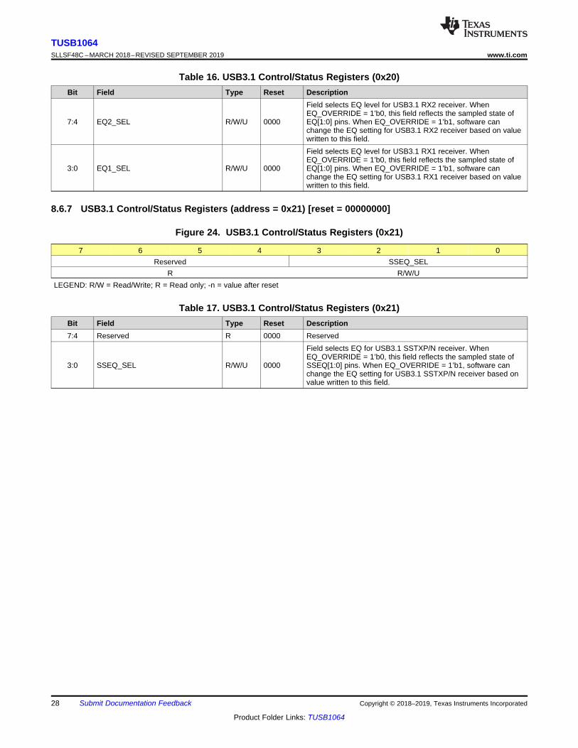
Table 16. USB3.1 Control/Status Registers (0x20)Bit Field Type Reset Description
7:4 EQ2_SEL R/W/U 0000
Field selects EQ level for USB3.1 RX2 receiver. WhenEQ_OVERRIDE = 1’b0, this field reflects the sampled state ofEQ[1:0] pins. When EQ_OVERRIDE = 1’b1, software canchange the EQ setting for USB3.1 RX2 receiver based on valuewritten to this field.
3:0 EQ1_SEL R/W/U 0000
Field selects EQ level for USB3.1 RX1 receiver. WhenEQ_OVERRIDE = 1’b0, this field reflects the sampled state ofEQ[1:0] pins. When EQ_OVERRIDE = 1’b1, software canchange the EQ setting for USB3.1 RX1 receiver based on valuewritten to this field.
8.6.7 USB3.1 Control/Status Registers (address = 0x21) [reset = 00000000]
Figure 24. USB3.1 Control/Status Registers (0x21)
7 6 5 4 3 2 1 0Reserved SSEQ_SEL
R R/W/ULEGEND: R/W = Read/Write; R = Read only; -n = value after reset
Table 17. USB3.1 Control/Status Registers (0x21)Bit Field Type Reset Description7:4 Reserved R 0000 Reserved
3:0 SSEQ_SEL R/W/U 0000
Field selects EQ for USB3.1 SSTXP/N receiver. WhenEQ_OVERRIDE = 1’b0, this field reflects the sampled state ofSSEQ[1:0] pins. When EQ_OVERRIDE = 1’b1, software canchange the EQ setting for USB3.1 SSTXP/N receiver based onvalue written to this field.
29
TUSB1064www.ti.com SLLSF48C –MARCH 2018–REVISED SEPTEMBER 2019
Product Folder Links: TUSB1064
Submit Documentation FeedbackCopyright © 2018–2019, Texas Instruments Incorporated
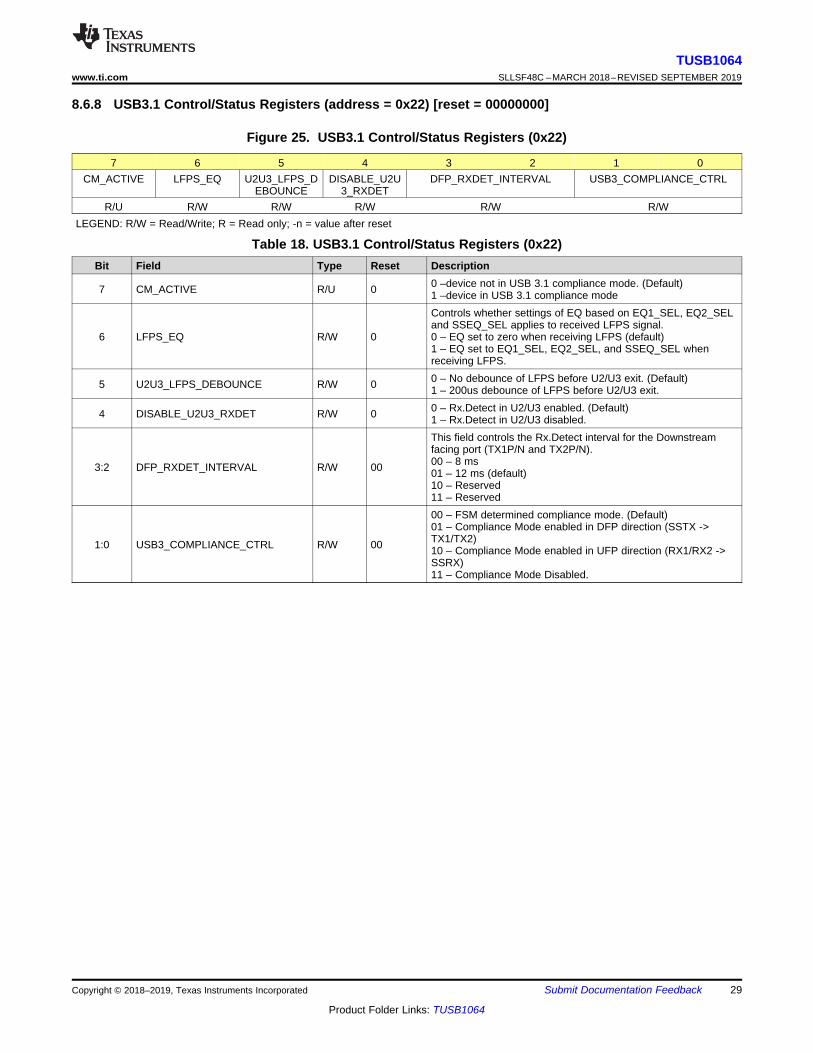
8.6.8 USB3.1 Control/Status Registers (address = 0x22) [reset = 00000000]
Figure 25. USB3.1 Control/Status Registers (0x22)
7 6 5 4 3 2 1 0CM_ACTIVE LFPS_EQ U2U3_LFPS_D
EBOUNCEDISABLE_U2U
3_RXDETDFP_RXDET_INTERVAL USB3_COMPLIANCE_CTRL
R/U R/W R/W R/W R/W R/WLEGEND: R/W = Read/Write; R = Read only; -n = value after reset
Table 18. USB3.1 Control/Status Registers (0x22)Bit Field Type Reset Description
7 CM_ACTIVE R/U 0 0 –device not in USB 3.1 compliance mode. (Default)1 –device in USB 3.1 compliance mode
6 LFPS_EQ R/W 0
Controls whether settings of EQ based on EQ1_SEL, EQ2_SELand SSEQ_SEL applies to received LFPS signal.0 – EQ set to zero when receiving LFPS (default)1 – EQ set to EQ1_SEL, EQ2_SEL, and SSEQ_SEL whenreceiving LFPS.
5 U2U3_LFPS_DEBOUNCE R/W 0 0 – No debounce of LFPS before U2/U3 exit. (Default)1 – 200us debounce of LFPS before U2/U3 exit.
4 DISABLE_U2U3_RXDET R/W 0 0 – Rx.Detect in U2/U3 enabled. (Default)1 – Rx.Detect in U2/U3 disabled.
3:2 DFP_RXDET_INTERVAL R/W 00
This field controls the Rx.Detect interval for the Downstreamfacing port (TX1P/N and TX2P/N).00 – 8 ms01 – 12 ms (default)10 – Reserved11 – Reserved
1:0 USB3_COMPLIANCE_CTRL R/W 00
00 – FSM determined compliance mode. (Default)01 – Compliance Mode enabled in DFP direction (SSTX ->TX1/TX2)10 – Compliance Mode enabled in UFP direction (RX1/RX2 ->SSRX)11 – Compliance Mode Disabled.
Copyright © 2017, Texas Instruments Incorporated
USB3.1
Hub
TUSB1064
DP 1.4
RX
Ty
pe
-C R
ece
pta
cle
BA
D
E
C
F
HG
DP0P
DP0N
DP1P
DP1N
DP2P
DP2N
DP3P
DP3N
TX1N
TX1P
TX2P
TX2N
RX1P
RX1N
RX2P
RX2N
PCB Trace of Length XEF PCB Trace of Length XAB
PCB Trace of Length XCDPCB Trace of Length XGH
SSRXP
SSRXN
SSTXP
SSTXN
30
TUSB1064SLLSF48C –MARCH 2018–REVISED SEPTEMBER 2019 www.ti.com
Product Folder Links: TUSB1064
Submit Documentation Feedback Copyright © 2018–2019, Texas Instruments Incorporated
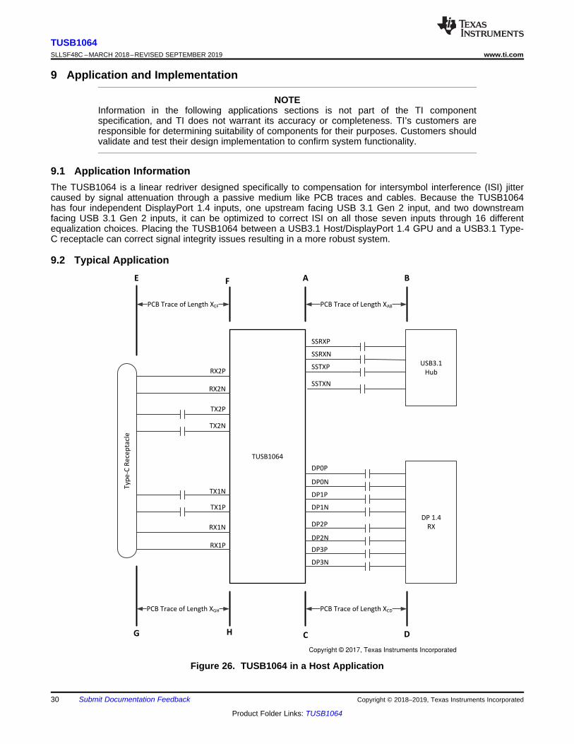
9 Application and Implementation
NOTEInformation in the following applications sections is not part of the TI componentspecification, and TI does not warrant its accuracy or completeness. TI’s customers areresponsible for determining suitability of components for their purposes. Customers shouldvalidate and test their design implementation to confirm system functionality.
9.1 Application InformationThe TUSB1064 is a linear redriver designed specifically to compensation for intersymbol interference (ISI) jittercaused by signal attenuation through a passive medium like PCB traces and cables. Because the TUSB1064has four independent DisplayPort 1.4 inputs, one upstream facing USB 3.1 Gen 2 input, and two downstreamfacing USB 3.1 Gen 2 inputs, it can be optimized to correct ISI on all those seven inputs through 16 differentequalization choices. Placing the TUSB1064 between a USB3.1 Host/DisplayPort 1.4 GPU and a USB3.1 Type-C receptacle can correct signal integrity issues resulting in a more robust system.
9.2 Typical Application
Figure 26. TUSB1064 in a Host Application
31
TUSB1064www.ti.com SLLSF48C –MARCH 2018–REVISED SEPTEMBER 2019
Product Folder Links: TUSB1064
Submit Documentation FeedbackCopyright © 2018–2019, Texas Instruments Incorporated
Typical Application (continued)9.2.1 Design RequirementsFor this design example, use the parameters shown in Table 19.
Table 19. Design ParametersPARAMETER VALUE
A to B PCB trace length, XAB 12 inchesC to D PCB trace length, XCD 12 inchesE to F PCB trace length, XEF 2 inchesG to H PCB trace length, XGH 2 inches
PCB trace width 4 milsAC-coupling capacitor (75 nF to 265 nF) 100 nF
VCC supply (3 V to 3.6 V) 3.3 VI2C Mode or GPIO Mode I2C Mode. (I2C_EN pin != "0")
1.8V or 3.3V I2C Interface 3.3V I2C. Pull-up the I2C_EN pin to 3.3V with a 1K ohm resistor.CTL1, EQ[1:0], SSEQ[1:0], and DPEQ[1:0] pin unconnected.
EQ setting for DisplayPort Lanes EQ Setting # 5 (Register 0x0A[4] = 1'b1, 0x10 = 0x55; 0x11 = 0x55)EQ setting for Downstream USB Data Path EQ Setting # 6 (Register 0x0A[4] = 1'b1, 0x20 = 0x66)
EQ setting for Upstream USB Data Path EQ Setting # 6 (Register 0x0A[4] = 1'b1, 0x21 = 0x08)
9.2.2 Detailed Design ProcedureA typical usage of the TUSB1064 device is shown in Figure 27. The device can be controlled either through itsGPIO pins or through its I2C interface. In the example shown below, a Type-C PD controller is used to configurethe device through the I2C interface. In I2C mode, the equalization settings for each receiver can beindependently controlled through I2C registers. For this reason, the configuration pin CTL1 and all of theequalization pins (EQ[1:0], SSEQ[1:0], and DPEQ[1:0]) can be left unconnected. If these pins are leftunconnected, the TUSB1064 7-bit I2C slave address will be 0x12 because both DPEQ/A1 and SSEQ0/A0 will beat pin level "F". If a different I2C slave address is desired, DPEQ/A1 and SSEQ0/A0 pins should be set to a levelwhich produces the desired I2C slave address.
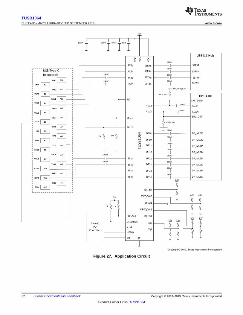
Copyright © 2017, Texas Instruments Incorporated
A11
A10
A9
A8
A7
A6
A5
A4
A3
A2
A1
A12
B2
B3
B4
B5
B6
B7
B8
B9
B10
B11
B12
B1GND
GND
GND
GND
TXP2
TXN2
VBUS
VBUS
VBUS
VBUS
RXP2
RXN2
SBU1
DN1
DP1
CC1
TXN1
TXP1
RXP1
RXN1
SBU2
CC2
DP2
DN2
RX2p
RX2n
TX2p
TX2n
TX1n
TX1p
RX1n
RX1p
SBU1
SBU2
SSTXp
SSTXn
SSRXp
SSRXn
DP0p
DP0n
DP1p
DP1n
DP2p
DP2n
DP3p
DP3n
AUXp
AUXn
SSRXP
SSRXN
SSTXP
SSTXN
TU
SB
10
64
AUXP
AUXN
DP_PWR (3.3V)
1M (± 5%)
100 nF
100 nF
100nF
100nF
100nF
100nF
100nF
100nF
100nF
100nF
100nF
100nF
100nF
100nF
100nF
100nF
100nF
100nF
DP_ML0P
DP_ML0N
DP_ML1P
DP_ML1N
DP_ML2P
DP_ML2N
DP_ML3P
DP_ML3N
USB 3.1 Hub
DP1.4 RX
USB Type-C
Receptacle
FLIP/SCL
2M2M
Type-C
PD
Controller
I2C_EN
SSEQ0/A0
SSEQ1
DPEQ0/A1
DPEQ1
EQ0
EQ1
R
3.3V
3.3V3.3V
3.3V3.3V3.3V3.3V
R
VI2C
VC
C
100nF 10PF
3.3V
100nF100nF
VC
C
VC
C
TPEN
NC
1M (± 5%)
SRC_DET
SRC_DET#
CTL1
CTL0/SDA
HPDIN
32
TUSB1064SLLSF48C –MARCH 2018–REVISED SEPTEMBER 2019 www.ti.com
Product Folder Links: TUSB1064
Submit Documentation Feedback Copyright © 2018–2019, Texas Instruments Incorporated
Figure 27. Application Circuit
SBU1
SBU2
AUXn
AUXp
TUSB1064
SBU2
SBU1
AUXP
AUXN
PD Controller
SBU2
SBU1
1M (+/-5%)
1M (+/-5%)
AUXP
AUXN
SRC_DET#
SRC_DET
100nF
100nF
DP SINK
3.3V
Make AUX connections as short as
possible to minimize stub effects
DP0
DP1
DP2
DP3
TX1
RX1
RX2
TX2
ML0
ML1
ML2
ML3
Copyright © 2017, Texas Instruments Incorporated
Typ
e-C
Re
ce
pta
cle
2M
2M
33
TUSB1064www.ti.com SLLSF48C –MARCH 2018–REVISED SEPTEMBER 2019
Product Folder Links: TUSB1064
Submit Documentation FeedbackCopyright © 2018–2019, Texas Instruments Incorporated
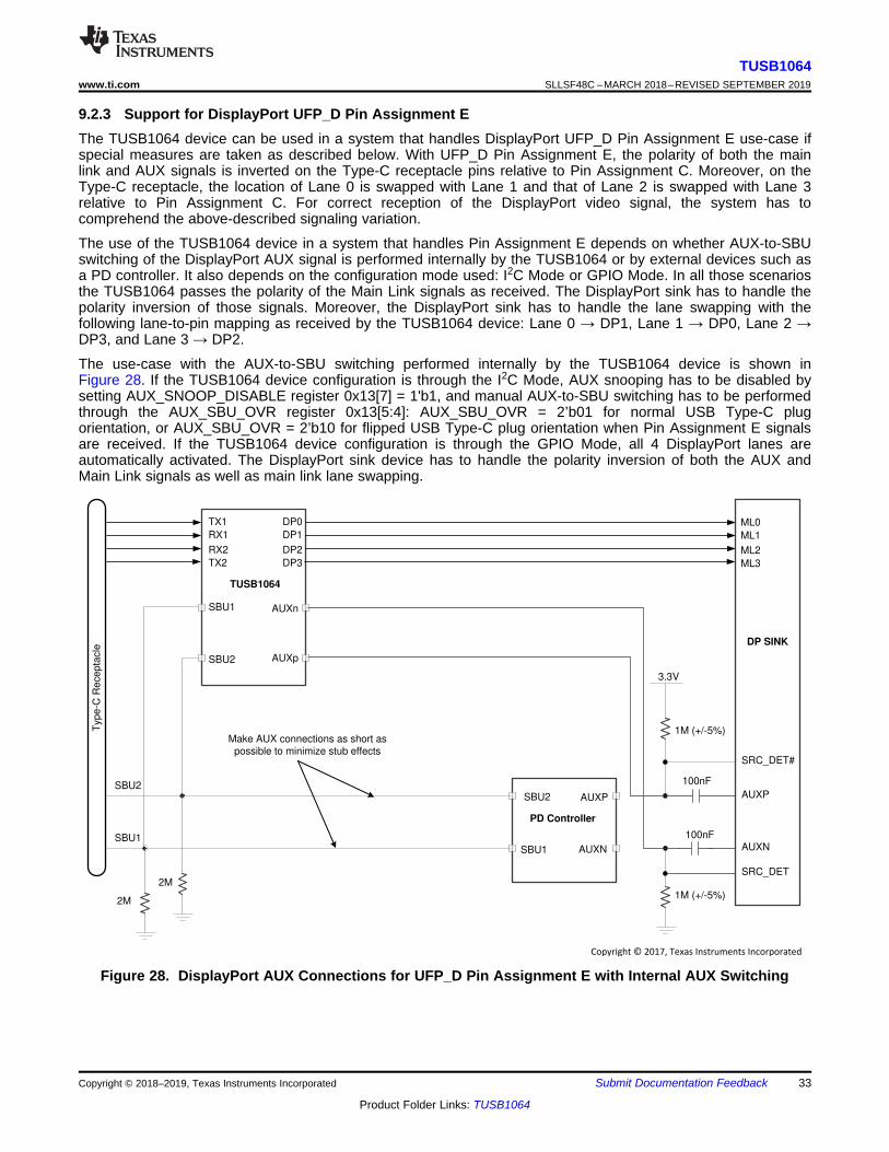
9.2.3 Support for DisplayPort UFP_D Pin Assignment EThe TUSB1064 device can be used in a system that handles DisplayPort UFP_D Pin Assignment E use-case ifspecial measures are taken as described below. With UFP_D Pin Assignment E, the polarity of both the mainlink and AUX signals is inverted on the Type-C receptacle pins relative to Pin Assignment C. Moreover, on theType-C receptacle, the location of Lane 0 is swapped with Lane 1 and that of Lane 2 is swapped with Lane 3relative to Pin Assignment C. For correct reception of the DisplayPort video signal, the system has tocomprehend the above-described signaling variation.
The use of the TUSB1064 device in a system that handles Pin Assignment E depends on whether AUX-to-SBUswitching of the DisplayPort AUX signal is performed internally by the TUSB1064 or by external devices such asa PD controller. It also depends on the configuration mode used: I2C Mode or GPIO Mode. In all those scenariosthe TUSB1064 passes the polarity of the Main Link signals as received. The DisplayPort sink has to handle thepolarity inversion of those signals. Moreover, the DisplayPort sink has to handle the lane swapping with thefollowing lane-to-pin mapping as received by the TUSB1064 device: Lane 0 → DP1, Lane 1 → DP0, Lane 2 →DP3, and Lane 3 → DP2.
The use-case with the AUX-to-SBU switching performed internally by the TUSB1064 device is shown inFigure 28. If the TUSB1064 device configuration is through the I2C Mode, AUX snooping has to be disabled bysetting AUX_SNOOP_DISABLE register 0x13[7] = 1'b1, and manual AUX-to-SBU switching has to be performedthrough the AUX_SBU_OVR register 0x13[5:4]: AUX_SBU_OVR = 2’b01 for normal USB Type-C plugorientation, or AUX_SBU_OVR = 2’b10 for flipped USB Type-C plug orientation when Pin Assignment E signalsare received. If the TUSB1064 device configuration is through the GPIO Mode, all 4 DisplayPort lanes areautomatically activated. The DisplayPort sink device has to handle the polarity inversion of both the AUX andMain Link signals as well as main link lane swapping.
Figure 28. DisplayPort AUX Connections for UFP_D Pin Assignment E with Internal AUX Switching
Frequency (GHz)
Insert
ion L
oss (
dB
)
0 2 4 6 8 10 12 14 16-60
-55
-50
-45
-40
-35
-30
-25
-20
-15
-10
-5
0
D009
Length=12in, Width=6milLength=16in, Width=6milLength=20in, Width=6milLength=24in, Width=6milLength=4in, Width=4milLength=8in, Width=10milLength=8in, Width=6mil
SBU1
SBU2
AUXn
AUXp
TUSB1064
SBU2
SBU1
AUXP
AUXN
PD Controller
SBU2
SBU1
1M (+/-5%)
1M (+/-5%)
AUXP
AUXN
SRC_DET#
SRC_DET
100nF
100nF
DP SINK
3.3V
Make AUX connections as short as
possible to minimize stub effects
DP0
DP1
DP2
DP3
TX1
RX1
RX2
TX2
ML0
ML1
ML2
ML3
Copyright © 2017, Texas Instruments Incorporated
Typ
e-C
Re
ce
pta
cle
2M
2M
34
TUSB1064SLLSF48C –MARCH 2018–REVISED SEPTEMBER 2019 www.ti.com
Product Folder Links: TUSB1064
Submit Documentation Feedback Copyright © 2018–2019, Texas Instruments Incorporated
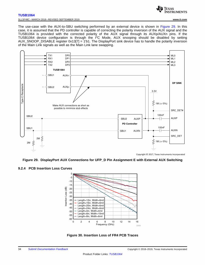
The use-case with the AUX-to-SBU switching performed by an external device is shown in Figure 29. In thiscase, it is assumed that the PD controller is capable of correcting the polarity inversion of the AUX signal and theTUSB1064 is provided with the corrected polarity of the AUX signal through its AUXp/AUXn pins. If theTUSB1064 device configuration is through the I2C Mode, AUX snooping should be disabled by settingAUX_SNOOP_DISABLE register 0x13[7] = 1'b1. The DisplayPort sink device has to handle the polarity inversionof the Main Link signals as well as the Main Link lane swapping.
Figure 29. DisplayPort AUX Connections for UFP_D Pin Assignment E with External AUX Switching
9.2.4 PCB Insertion Loss Curves
Figure 30. Insertion Loss of FR4 PCB Traces
USB Host
GPU
TUSB1046A-DCI
Typ
e-C
Re
ce
pta
cle
PD Controller
USB Hub
DP RX
TUSB1064
PD Controller
SSTX
SSRX SSTX
SSRX
DP0
DP1
DP2
DP3
AUXp
AUXn
SBU1
SBU2
CC1
CC2Control
HPD HPD
Control
CC1
CC2
DP0
DP1
DP2
DP3
AUXn
AUXpSBU1
SBU2
CTLFLIP 0 1
CTL1/0/FLIP=L/H/L
1 Port USB
CTLFLIP 0 1
TX1
TX2
RX1
RX2
TX2
TX1
RX2
RX1
HPDIN HPDIN
D+/-
Typ
e-C
Re
ce
pta
cle
D+/-
CTL1/0/FLIP=L/H/L
Copyright © 2017, Texas Instruments Incorporated
35
TUSB1064www.ti.com SLLSF48C –MARCH 2018–REVISED SEPTEMBER 2019
Product Folder Links: TUSB1064
Submit Documentation FeedbackCopyright © 2018–2019, Texas Instruments Incorporated
9.3 System Examples
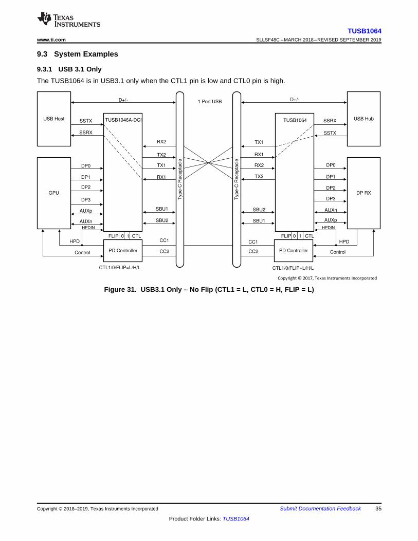
9.3.1 USB 3.1 OnlyThe TUSB1064 is in USB3.1 only when the CTL1 pin is low and CTL0 pin is high.
Figure 31. USB3.1 Only – No Flip (CTL1 = L, CTL0 = H, FLIP = L)
USB Host
GPU
TUSB1046A-DCI
Typ
e-C
Re
ce
pta
cle
PD Controller
USB Hub
DP RX
TUSB1064
PD Controller
D+/-
SSTX
SSRX SSTX
SSRX
DP0
DP1
DP2
DP3
AUXp
AUXn
SBU1
SBU2
CC1
CC2Control
HPD HPD
Control
CC1
CC2
DP0
DP1
DP2
DP3
AUXn
AUXp
SBU2
CTL1/0/FLIP=L/H/H
1 Port USB
CTLFLIP 0 1 CTLFLIP 0 1
TX1
TX2
RX1
RX2
TX2
TX1
RX2
RX1
HPDIN HPDIN
Typ
e-C
Re
ce
pta
cle
D+/-
SBU1
CTL1/0/FLIP=L/H/H
Copyright © 2017, Texas Instruments Incorporated
36
TUSB1064SLLSF48C –MARCH 2018–REVISED SEPTEMBER 2019 www.ti.com
Product Folder Links: TUSB1064
Submit Documentation Feedback Copyright © 2018–2019, Texas Instruments Incorporated
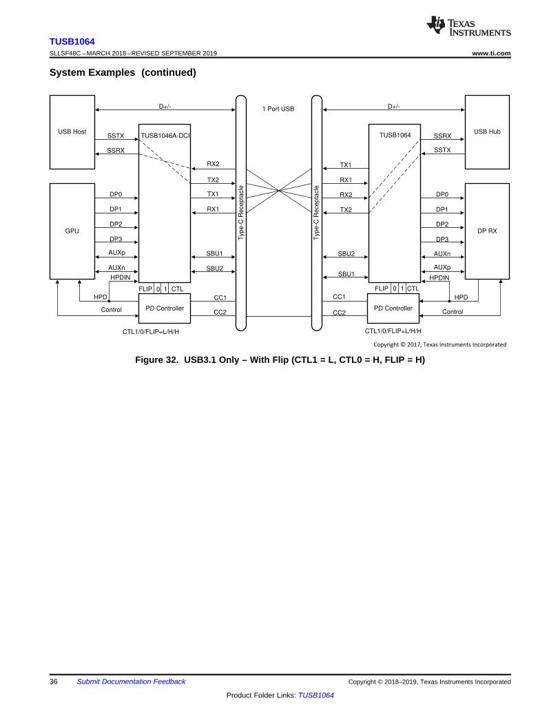
System Examples (continued)
Figure 32. USB3.1 Only – With Flip (CTL1 = L, CTL0 = H, FLIP = H)
USB Host
GPU
TUSB1046A-DCI
Typ
e-C
Re
ce
pta
cle
PD Controller
USB Hub
DP RX
TUSB1064
PD Controller
SSTX
SSRX SSTX
SSRX
DP0
DP1
DP2
DP3
AUXp
AUXn
SBU1
SBU2
CC1
CC2Control
HPD HPD
Control
CC1
CC2
DP0
DP1
DP2
DP3
AUXn
AUXpSBU2
SBU1
CTL1/0/FLIP=H/H/L CTL1/0/FLIP=H/H/L
1 Port USB &
2 Lane DP
CTLFLIP 0 1CTLFLIP 0 1
TX1
TX2
RX1
RX2
TX2
TX1
RX2
RX1
HPDIN HPDIN
D+/- D+/-
Typ
e-C
Re
ce
pta
cle
Copyright © 2016, Texas Instruments Incorporated
37
TUSB1064www.ti.com SLLSF48C –MARCH 2018–REVISED SEPTEMBER 2019
Product Folder Links: TUSB1064
Submit Documentation FeedbackCopyright © 2018–2019, Texas Instruments Incorporated
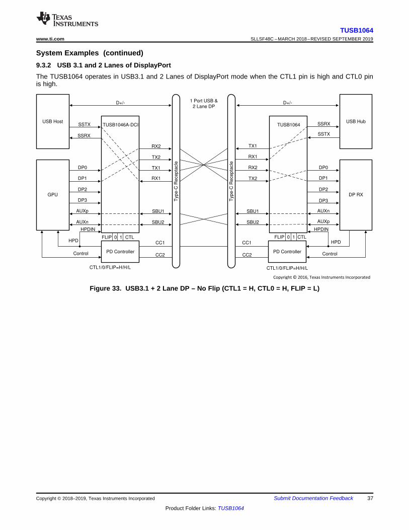
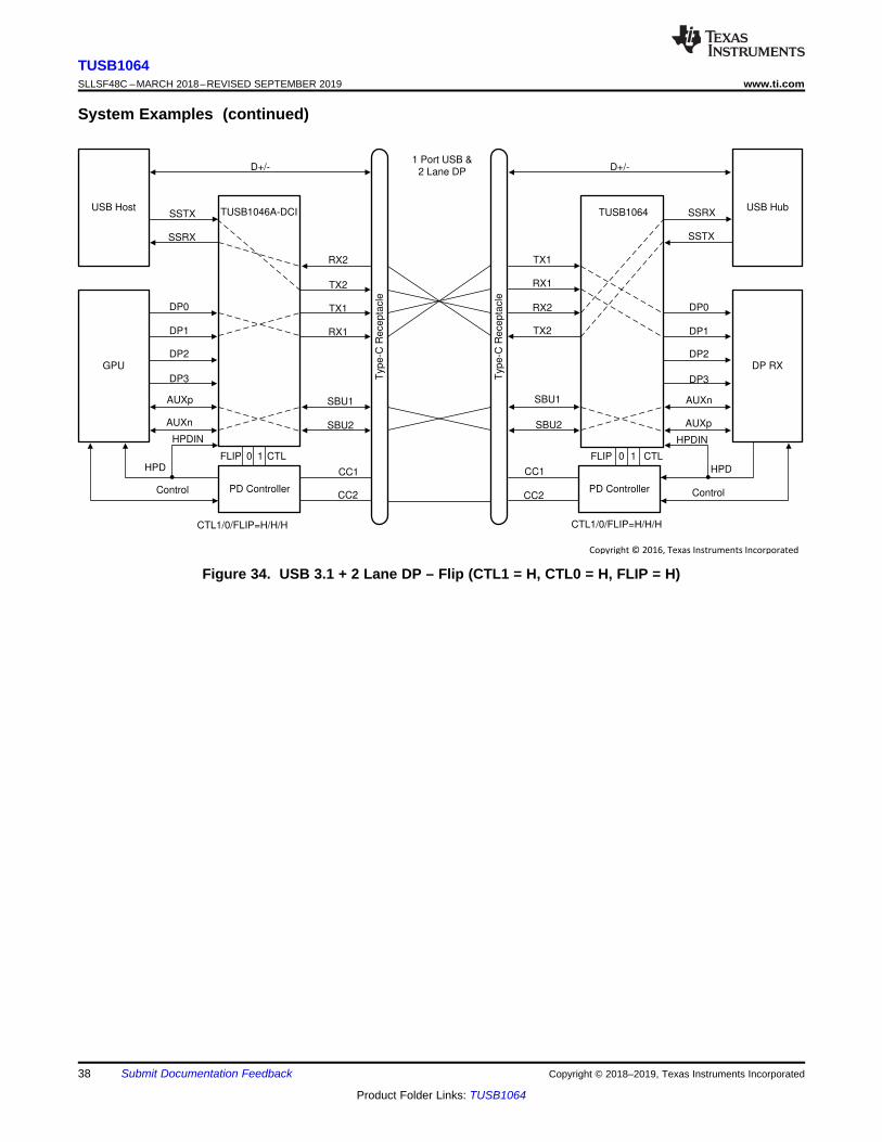
System Examples (continued)9.3.2 USB 3.1 and 2 Lanes of DisplayPortThe TUSB1064 operates in USB3.1 and 2 Lanes of DisplayPort mode when the CTL1 pin is high and CTL0 pinis high.
Figure 33. USB3.1 + 2 Lane DP – No Flip (CTL1 = H, CTL0 = H, FLIP = L)
USB Host
GPU
TUSB1046A-DCI
PD Controller
USB Hub
DP RX
TUSB1064
Typ
e-C
Re
ce
pta
cle
PD Controller
SSTX
SSRX SSTX
SSRX
DP0
DP1
DP2
DP3
AUXp
AUXn
SBU1
SBU2
CC1
CC2Control
HPD HPD
Control
CC1
CC2
DP0
DP1
DP2
DP3
AUXp
AUXn
SBU2
SBU1
CTL1/0/FLIP=H/H/H CTL1/0/FLIP=H/H/H
1 Port USB &
2 Lane DP
CTLFLIP 0 1CTLFLIP 0 1
TX1
TX2
RX1
RX2
TX2
TX1
RX2
RX1
HPDIN HPDIN
D+/- D+/-
Typ
e-C
Re
ce
pta
cle
Copyright © 2016, Texas Instruments Incorporated
38
TUSB1064SLLSF48C –MARCH 2018–REVISED SEPTEMBER 2019 www.ti.com
Product Folder Links: TUSB1064
Submit Documentation Feedback Copyright © 2018–2019, Texas Instruments Incorporated
System Examples (continued)
Figure 34. USB 3.1 + 2 Lane DP – Flip (CTL1 = H, CTL0 = H, FLIP = H)
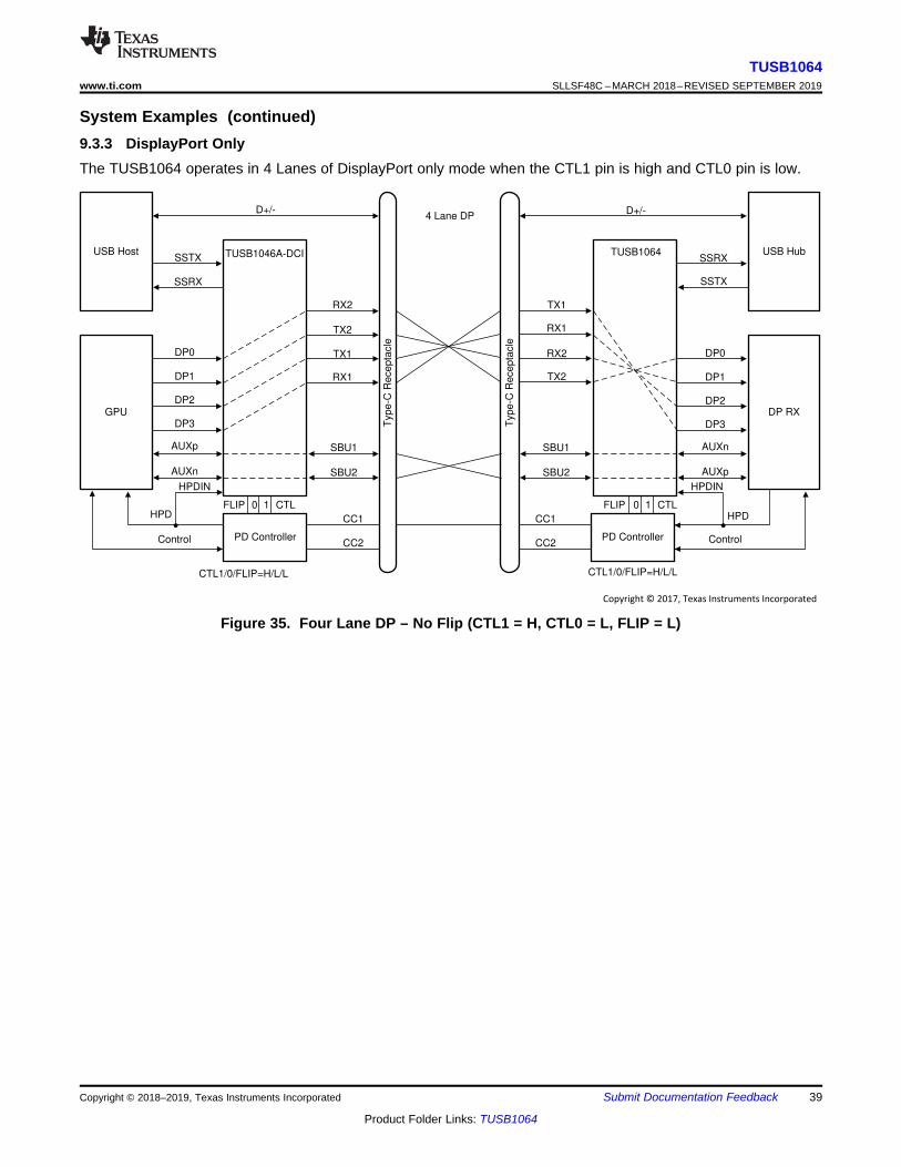
USB Host
GPU
TUSB1046A-DCI
Typ
e-C
Re
ce
pta
cle
PD Controller
USB Hub
DP RX
TUSB1064
PD Controller
D+/-
SSTX
SSRX SSTX
SSRX
DP0
DP1
DP2
DP3
AUXp
AUXn
SBU1
SBU2
CC1
CC2Control
HPD HPD
Control
CTL1/0/FLIP=H/L/L CTL1/0/FLIP=H/L/L
4 Lane DP
CTLFLIP 0 1 CTLFLIP 0 1
TX1
TX2
RX1
RX2
TX2
TX1
RX2
RX1
HPDIN HPDIN
D+/-
Typ
e-C
Re
ce
pta
cle
CC1
CC2
SBU1
SBU2
DP0
DP1
DP2
DP3
AUXn
AUXp
Copyright © 2017, Texas Instruments Incorporated
39
TUSB1064www.ti.com SLLSF48C –MARCH 2018–REVISED SEPTEMBER 2019
Product Folder Links: TUSB1064
Submit Documentation FeedbackCopyright © 2018–2019, Texas Instruments Incorporated
System Examples (continued)9.3.3 DisplayPort OnlyThe TUSB1064 operates in 4 Lanes of DisplayPort only mode when the CTL1 pin is high and CTL0 pin is low.
Figure 35. Four Lane DP – No Flip (CTL1 = H, CTL0 = L, FLIP = L)
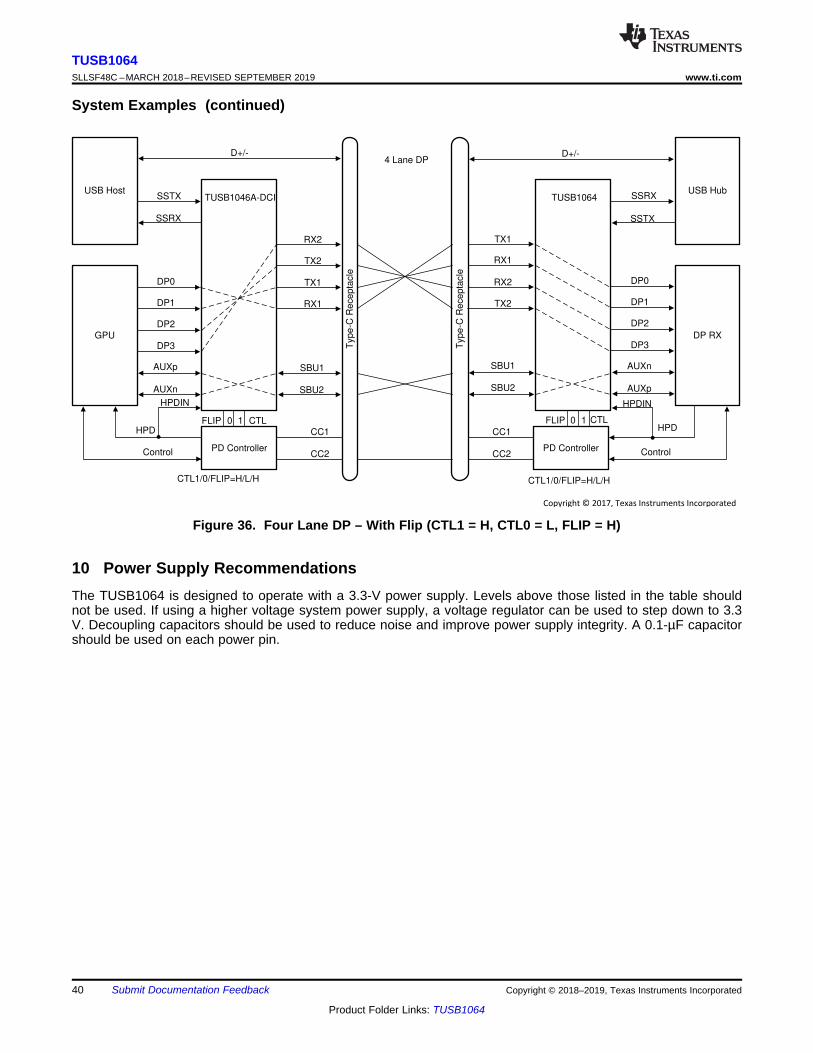
USB Host
GPU
TUSB1046A-DCI
Typ
e-C
Re
ce
pta
cle
PD Controller
USB Hub
DP RX
TUSB1064
PD Controller
D+/-
SSTX
SSRX SSTX
SSRX
DP0
DP1
DP2
DP3
AUXp
AUXn
SBU1
SBU2
CC1
CC2Control
HPD HPD
Control
TX1
TX2
RX1
RX2
TX2
TX1
RX2
RX1
CTL1/0/FLIP=H/L/H CTL1/0/FLIP=H/L/H
4 Lane DP
CTLFLIP 0 1 CTLFLIP 0 1
HPDIN HPDIN
D+/-
Typ
e-C
Re
ce
pta
cle
SBU1
SBU2
CC1
CC2
DP0
DP1
DP2
DP3
AUXn
AUXp
Copyright © 2017, Texas Instruments Incorporated
40
TUSB1064SLLSF48C –MARCH 2018–REVISED SEPTEMBER 2019 www.ti.com
Product Folder Links: TUSB1064
Submit Documentation Feedback Copyright © 2018–2019, Texas Instruments Incorporated
System Examples (continued)
Figure 36. Four Lane DP – With Flip (CTL1 = H, CTL0 = L, FLIP = H)
10 Power Supply RecommendationsThe TUSB1064 is designed to operate with a 3.3-V power supply. Levels above those listed in the table shouldnot be used. If using a higher voltage system power supply, a voltage regulator can be used to step down to 3.3V. Decoupling capacitors should be used to reduce noise and improve power supply integrity. A 0.1-µF capacitorshould be used on each power pin.
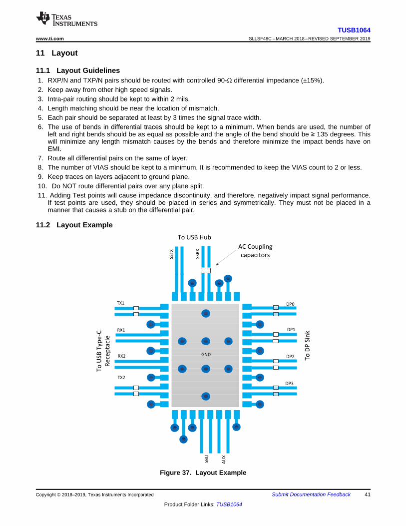
AC Coupling
capacitors
DP3
DP1
DP2
DP0
To
US
B T
yp
e-C
Re
cep
tacl
e
GND
SS
RX
SS
TX
To USB Hub
RX2
TX1
TX2
RX1
To
DP
Sin
k
SB
U
AU
X
41
TUSB1064www.ti.com SLLSF48C –MARCH 2018–REVISED SEPTEMBER 2019
Product Folder Links: TUSB1064
Submit Documentation FeedbackCopyright © 2018–2019, Texas Instruments Incorporated
11 Layout
11.1 Layout Guidelines1. RXP/N and TXP/N pairs should be routed with controlled 90-Ω differential impedance (±15%).2. Keep away from other high speed signals.3. Intra-pair routing should be kept to within 2 mils.4. Length matching should be near the location of mismatch.5. Each pair should be separated at least by 3 times the signal trace width.6. The use of bends in differential traces should be kept to a minimum. When bends are used, the number of
left and right bends should be as equal as possible and the angle of the bend should be ≥ 135 degrees. Thiswill minimize any length mismatch causes by the bends and therefore minimize the impact bends have onEMI.
7. Route all differential pairs on the same of layer.8. The number of VIAS should be kept to a minimum. It is recommended to keep the VIAS count to 2 or less.9. Keep traces on layers adjacent to ground plane.10. Do NOT route differential pairs over any plane split.11. Adding Test points will cause impedance discontinuity, and therefore, negatively impact signal performance.
If test points are used, they should be placed in series and symmetrically. They must not be placed in amanner that causes a stub on the differential pair.
11.2 Layout Example
Figure 37. Layout Example
42
TUSB1064SLLSF48C –MARCH 2018–REVISED SEPTEMBER 2019 www.ti.com
Product Folder Links: TUSB1064
Submit Documentation Feedback Copyright © 2018–2019, Texas Instruments Incorporated
12 Device and Documentation Support
12.1 Receiving Notification of Documentation UpdatesTo receive notification of documentation updates, navigate to the device product folder on ti.com. In the upperright corner, click on Alert me to register and receive a weekly digest of any product information that haschanged. For change details, review the revision history included in any revised document.
12.2 Community ResourcesTI E2E™ support forums are an engineer's go-to source for fast, verified answers and design help — straightfrom the experts. Search existing answers or ask your own question to get the quick design help you need.
Linked content is provided "AS IS" by the respective contributors. They do not constitute TI specifications and donot necessarily reflect TI's views; see TI's Terms of Use.
12.3 TrademarksE2E is a trademark of Texas Instruments.USB Type-C is a trademark of USB Implementers Forum.DisplayPort is a trademark of VESA.All other trademarks are the property of their respective owners.
12.4 Electrostatic Discharge CautionThis integrated circuit can be damaged by ESD. Texas Instruments recommends that all integrated circuits be handled withappropriate precautions. Failure to observe proper handling and installation procedures can cause damage.
ESD damage can range from subtle performance degradation to complete device failure. Precision integrated circuits may be moresusceptible to damage because very small parametric changes could cause the device not to meet its published specifications.
12.5 GlossarySLYZ022 — TI Glossary.
This glossary lists and explains terms, acronyms, and definitions.
13 Mechanical, Packaging, and Orderable InformationThe following pages include mechanical, packaging, and orderable information. This information is the mostcurrent data available for the designated devices. This data is subject to change without notice and revision ofthis document. For browser-based versions of this data sheet, refer to the left-hand navigation.
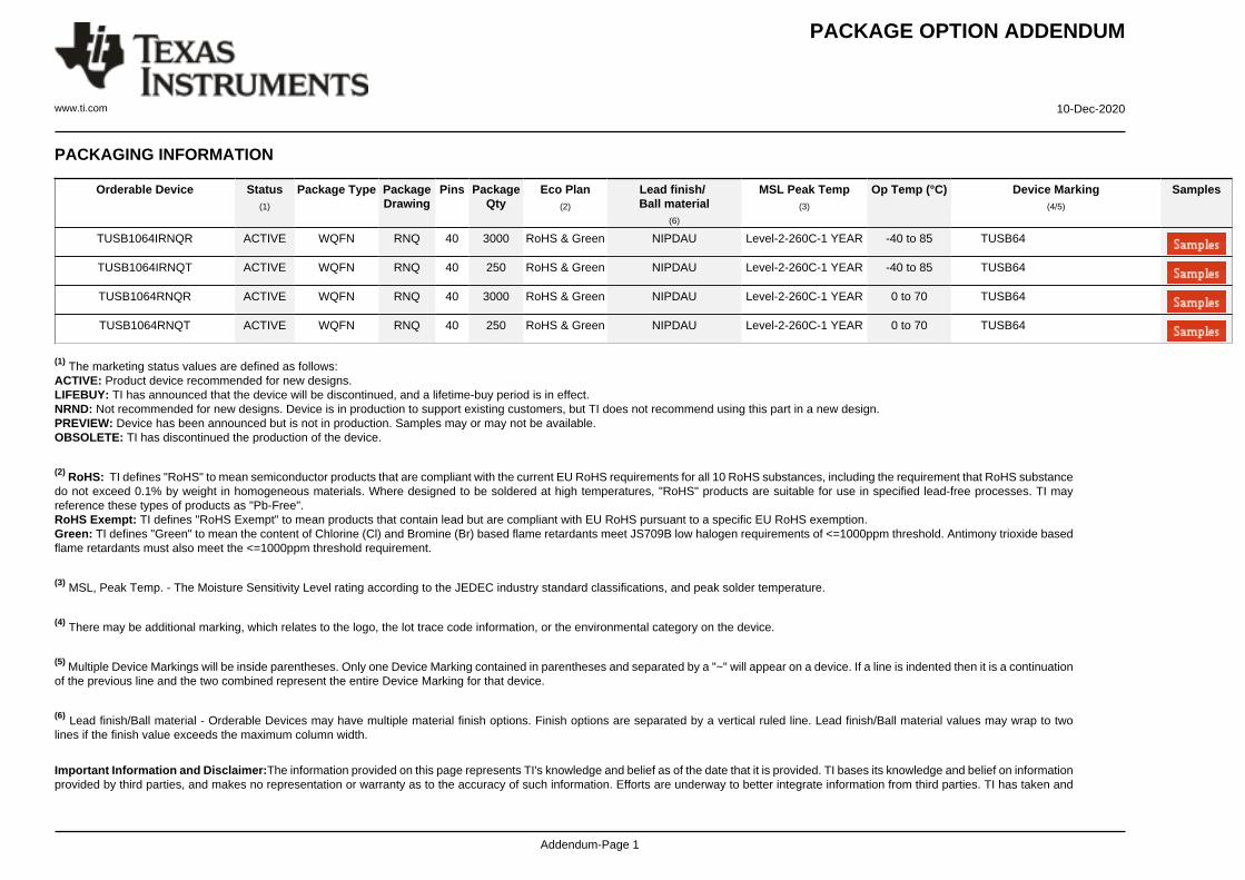
PACKAGE OPTION ADDENDUM
www.ti.com 10-Dec-2020
Addendum-Page 1
PACKAGING INFORMATION
Orderable Device Status(1)
Package Type PackageDrawing
Pins PackageQty
Eco Plan(2)
Lead finish/Ball material
(6)
MSL Peak Temp(3)
Op Temp (°C) Device Marking(4/5)
Samples
TUSB1064IRNQR ACTIVE WQFN RNQ 40 3000 RoHS & Green NIPDAU Level-2-260C-1 YEAR -40 to 85 TUSB64
TUSB1064IRNQT ACTIVE WQFN RNQ 40 250 RoHS & Green NIPDAU Level-2-260C-1 YEAR -40 to 85 TUSB64
TUSB1064RNQR ACTIVE WQFN RNQ 40 3000 RoHS & Green NIPDAU Level-2-260C-1 YEAR 0 to 70 TUSB64
TUSB1064RNQT ACTIVE WQFN RNQ 40 250 RoHS & Green NIPDAU Level-2-260C-1 YEAR 0 to 70 TUSB64
(1) The marketing status values are defined as follows:ACTIVE: Product device recommended for new designs.LIFEBUY: TI has announced that the device will be discontinued, and a lifetime-buy period is in effect.NRND: Not recommended for new designs. Device is in production to support existing customers, but TI does not recommend using this part in a new design.PREVIEW: Device has been announced but is not in production. Samples may or may not be available.OBSOLETE: TI has discontinued the production of the device.
(2) RoHS: TI defines "RoHS" to mean semiconductor products that are compliant with the current EU RoHS requirements for all 10 RoHS substances, including the requirement that RoHS substancedo not exceed 0.1% by weight in homogeneous materials. Where designed to be soldered at high temperatures, "RoHS" products are suitable for use in specified lead-free processes. TI mayreference these types of products as "Pb-Free".RoHS Exempt: TI defines "RoHS Exempt" to mean products that contain lead but are compliant with EU RoHS pursuant to a specific EU RoHS exemption.Green: TI defines "Green" to mean the content of Chlorine (Cl) and Bromine (Br) based flame retardants meet JS709B low halogen requirements of <=1000ppm threshold. Antimony trioxide basedflame retardants must also meet the <=1000ppm threshold requirement.
(3) MSL, Peak Temp. - The Moisture Sensitivity Level rating according to the JEDEC industry standard classifications, and peak solder temperature.
(4) There may be additional marking, which relates to the logo, the lot trace code information, or the environmental category on the device.
(5) Multiple Device Markings will be inside parentheses. Only one Device Marking contained in parentheses and separated by a "~" will appear on a device. If a line is indented then it is a continuationof the previous line and the two combined represent the entire Device Marking for that device.
(6) Lead finish/Ball material - Orderable Devices may have multiple material finish options. Finish options are separated by a vertical ruled line. Lead finish/Ball material values may wrap to twolines if the finish value exceeds the maximum column width.
Important Information and Disclaimer:The information provided on this page represents TI's knowledge and belief as of the date that it is provided. TI bases its knowledge and belief on informationprovided by third parties, and makes no representation or warranty as to the accuracy of such information. Efforts are underway to better integrate information from third parties. TI has taken and
PACKAGE OPTION ADDENDUM
www.ti.com 10-Dec-2020
Addendum-Page 2
continues to take reasonable steps to provide representative and accurate information but may not have conducted destructive testing or chemical analysis on incoming materials and chemicals.TI and TI suppliers consider certain information to be proprietary, and thus CAS numbers and other limited information may not be available for release.
In no event shall TI's liability arising out of such information exceed the total purchase price of the TI part(s) at issue in this document sold by TI to Customer on an annual basis.
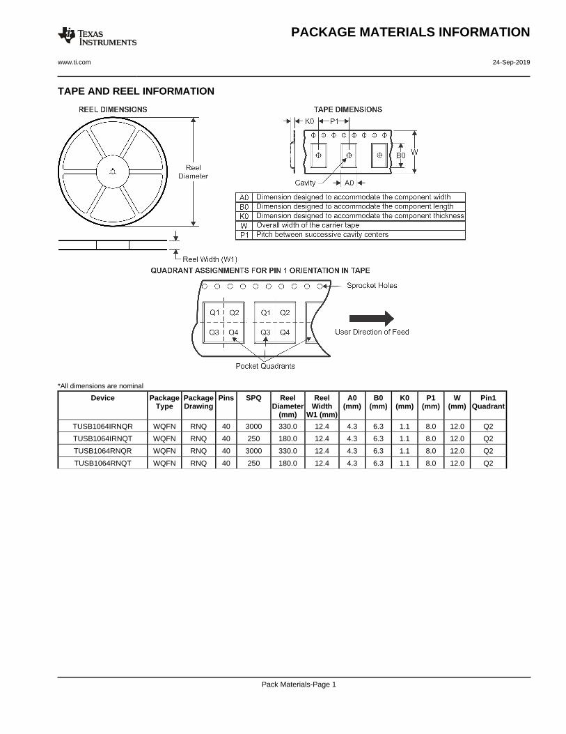
TAPE AND REEL INFORMATION
*All dimensions are nominal
Device PackageType
PackageDrawing
Pins SPQ ReelDiameter
(mm)
ReelWidth
W1 (mm)
A0(mm)
B0(mm)
K0(mm)
P1(mm)
W(mm)
Pin1Quadrant
TUSB1064IRNQR WQFN RNQ 40 3000 330.0 12.4 4.3 6.3 1.1 8.0 12.0 Q2
TUSB1064IRNQT WQFN RNQ 40 250 180.0 12.4 4.3 6.3 1.1 8.0 12.0 Q2
TUSB1064RNQR WQFN RNQ 40 3000 330.0 12.4 4.3 6.3 1.1 8.0 12.0 Q2
TUSB1064RNQT WQFN RNQ 40 250 180.0 12.4 4.3 6.3 1.1 8.0 12.0 Q2
PACKAGE MATERIALS INFORMATION
www.ti.com 24-Sep-2019
Pack Materials-Page 1
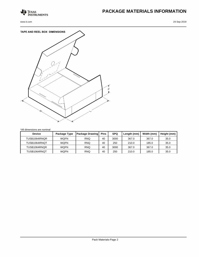
*All dimensions are nominal
Device Package Type Package Drawing Pins SPQ Length (mm) Width (mm) Height (mm)
TUSB1064IRNQR WQFN RNQ 40 3000 367.0 367.0 35.0
TUSB1064IRNQT WQFN RNQ 40 250 210.0 185.0 35.0
TUSB1064RNQR WQFN RNQ 40 3000 367.0 367.0 35.0
TUSB1064RNQT WQFN RNQ 40 250 210.0 185.0 35.0
PACKAGE MATERIALS INFORMATION
www.ti.com 24-Sep-2019
Pack Materials-Page 2
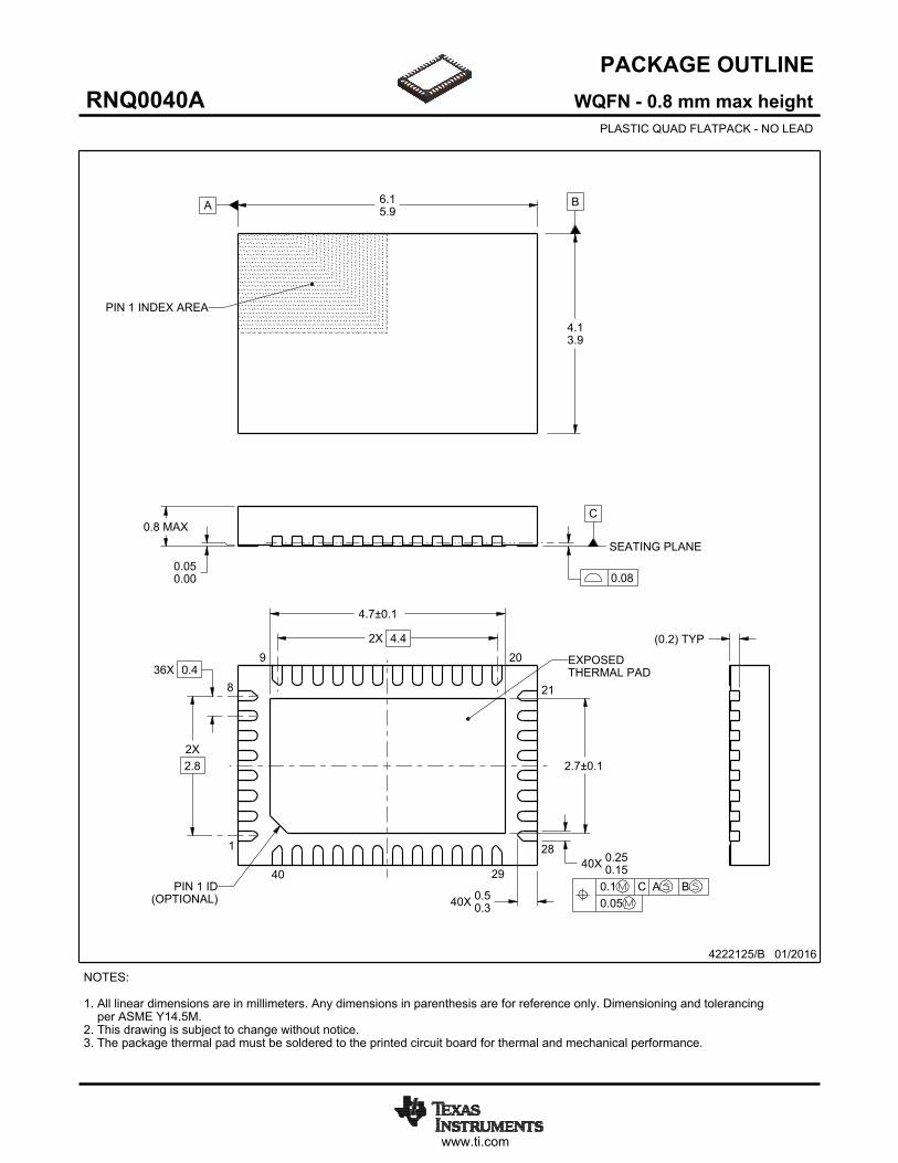
www.ti.com
PACKAGE OUTLINE
C
40X 0.250.15
4.7±0.1
40X 0.50.3
0.8 MAX
(0.2) TYP
0.050.00
36X 0.4
2X2.8
2X 4.4
2.7±0.1
A 6.15.9
B
4.13.9
WQFN - 0.8 mm max heightRNQ0040APLASTIC QUAD FLATPACK - NO LEAD
4222125/B 01/2016
PIN 1 INDEX AREA
0.08
SEATING PLANE
1
8 21
28
9 20
40 29
(OPTIONAL)PIN 1 ID 0.1 C A B
0.05
EXPOSEDTHERMAL PAD
NOTES: 1. All linear dimensions are in millimeters. Any dimensions in parenthesis are for reference only. Dimensioning and tolerancing per ASME Y14.5M. 2. This drawing is subject to change without notice. 3. The package thermal pad must be soldered to the printed circuit board for thermal and mechanical performance.
SCALE 2.500
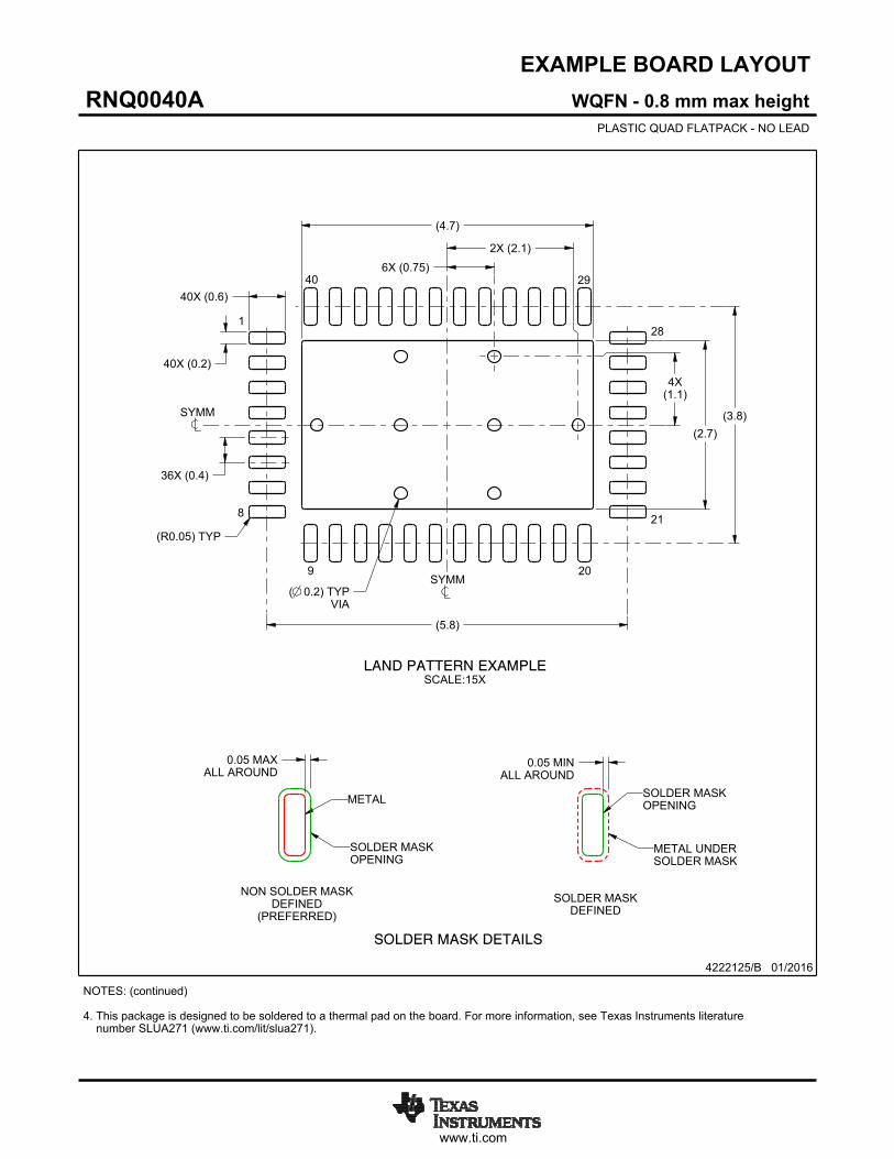
www.ti.com
EXAMPLE BOARD LAYOUT
0.05 MINALL AROUND
0.05 MAXALL AROUND
40X (0.2)
40X (0.6)
( ) TYPVIA
0.2
36X (0.4)
(3.8)
(5.8)
4X(1.1)
(4.7)
(R ) TYP0.05
(2.7)
2X (2.1)6X (0.75)
WQFN - 0.8 mm max heightRNQ0040APLASTIC QUAD FLATPACK - NO LEAD
4222125/B 01/2016
SYMM
1
8
9 20
21
28
2940
SYMM
LAND PATTERN EXAMPLESCALE:15X
NOTES: (continued) 4. This package is designed to be soldered to a thermal pad on the board. For more information, see Texas Instruments literature number SLUA271 (www.ti.com/lit/slua271).
SOLDER MASKOPENING
METAL UNDERSOLDER MASK
SOLDER MASKDEFINED
METAL
SOLDER MASKOPENING
SOLDER MASK DETAILS
NON SOLDER MASKDEFINED
(PREFERRED)
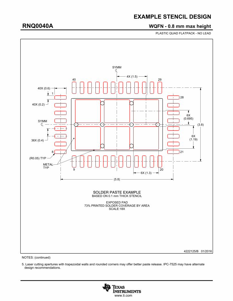
www.ti.com
EXAMPLE STENCIL DESIGN
40X (0.6)
40X (0.2)
36X (0.4)
(5.8)
(3.8)
6X (1.3)
6X(0.695)
4X (1.5)
(R ) TYP0.05
6X(1.19)
WQFN - 0.8 mm max heightRNQ0040APLASTIC QUAD FLATPACK - NO LEAD
4222125/B 01/2016
NOTES: (continued) 5. Laser cutting apertures with trapezoidal walls and rounded corners may offer better paste release. IPC-7525 may have alternate design recommendations.
SYMM
METALTYP
SOLDER PASTE EXAMPLEBASED ON 0.1 mm THICK STENCIL
EXPOSED PAD
73% PRINTED SOLDER COVERAGE BY AREASCALE:18X
SYMM
1
8
9 20
21
28
2940
IMPORTANT NOTICE AND DISCLAIMER
TI PROVIDES TECHNICAL AND RELIABILITY DATA (INCLUDING DATASHEETS), DESIGN RESOURCES (INCLUDING REFERENCE DESIGNS), APPLICATION OR OTHER DESIGN ADVICE, WEB TOOLS, SAFETY INFORMATION, AND OTHER RESOURCES “AS IS” AND WITH ALL FAULTS, AND DISCLAIMS ALL WARRANTIES, EXPRESS AND IMPLIED, INCLUDING WITHOUT LIMITATION ANY IMPLIED WARRANTIES OF MERCHANTABILITY, FITNESS FOR A PARTICULAR PURPOSE OR NON-INFRINGEMENT OF THIRD PARTY INTELLECTUAL PROPERTY RIGHTS.These resources are intended for skilled developers designing with TI products. You are solely responsible for (1) selecting the appropriate TI products for your application, (2) designing, validating and testing your application, and (3) ensuring your application meets applicable standards, and any other safety, security, or other requirements. These resources are subject to change without notice. TI grants you permission to use these resources only for development of an application that uses the TI products described in the resource. Other reproduction and display of these resources is prohibited. No license is granted to any other TI intellectual property right or to any third party intellectual property right. TI disclaims responsibility for, and you will fully indemnify TI and its representatives against, any claims, damages, costs, losses, and liabilities arising out of your use of these resources.TI’s products are provided subject to TI’s Terms of Sale (www.ti.com/legal/termsofsale.html) or other applicable terms available either on ti.com or provided in conjunction with such TI products. TI’s provision of these resources does not expand or otherwise alter TI’s applicable warranties or warranty disclaimers for TI products.
Mailing Address: Texas Instruments, Post Office Box 655303, Dallas, Texas 75265Copyright © 2020, Texas Instruments Incorporated