Embed Size (px)
Citation preview
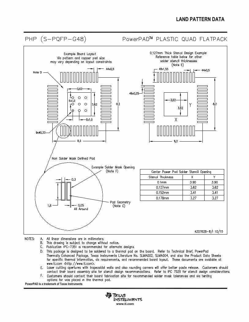
Personal
Computer
USB 3.0
HDD
USB 3.0
Hub
USB 2.0 Connection
USB 3.0 Connection
USB 3.0 Hub
USB 3.0 Device
USB 2.0 Device
USB 1.x Device
USB 1.x Connection
USB 3.0
HDD
USB 2.0
Bluray
USB 2.0
Hub
USB 2.0
Webcam
USB 1.1
Mouse
USB 2.0
HDDTUSB8020B
Product
Folder
Order
Now
Technical
Documents
Tools &
Software
Support &Community
An IMPORTANT NOTICE at the end of this data sheet addresses availability, warranty, changes, use in safety-critical applications,intellectual property matters and other important disclaimers. PRODUCTION DATA.
TUSB8020BSLLSEF6C –JULY 2014–REVISED JUNE 2017
TUSB8020B Two-Port USB 3.0 Hub
1
1 Features1• Two-Port USB 3.0 Compliant Hub, USBIF
TID#330000057• USB 2.0 Hub Features
– Multi-Transaction Translator (MTT) Hub: TwoTransaction Translators
– Four Asynchronous Endpoint Buffers PerTransaction Translator
• Supports Battery Charging– CDP Mode (Upstream Port Connected)– DCP Mode (Upstream Port Unconnected)– DCP Mode Complies With Chinese
Telecommunications Industry Standard YD/T1591-2009
• Support D+/D– Divider Mode• Supports Operation as a USB 3.0 or USB 2.0
Compound Device• Per Port or Ganged Power Switching and
Overcurrent Notification Inputs• OTP ROM, Serial EEPRO,M or I2C/SMBus Slave
Interface for Custom Configurations:– VID and PID– Port Customizations– Manufacturer and Product Strings (not by OTP
ROM)– Serial Number (not by OTP ROM)
• Application Feature Selection Using TerminalSelection or EEPROM/ or I2C/SMBus SlaveInterface
• Provides 128-Bit Universally Unique Identifier(UUID)
• Supports On-Board and In-System OTP/EEPROMProgramming Through the USB 2.0 UpstreamPort
• Single Clock Input, 24-MHz Crystal or Oscillator• No Special Driver Requirements; Works
Seamlessly on any Operating System With USBStack Support
• 48-Pin HTQFP Package (PHP)
2 Applications• Computer Systems• Docking Stations• Monitors• Set-Top Boxes
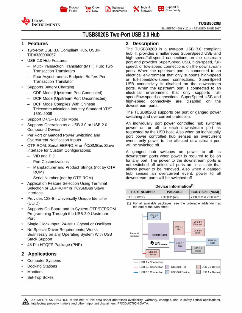
3 DescriptionThe TUSB8020B is a two-port USB 3.0 complianthub. It provides simultaneous SuperSpeed USB andhigh-speed/full-speed connections on the upstreamport and provides SuperSpeed USB, high-speed, full-speed, or low-speed connections on the downstreamports. When the upstream port is connected to anelectrical environment that only supports high-speedor full-speed/low-speed connections, SuperSpeedUSB connectivity is disabled on the downstreamports. When the upstream port is connected to anelectrical environment that only supports full-speed/low-speed connections, SuperSpeed USB andhigh-speed connectivity are disabled on thedownstream ports.
The TUSB8020B supports per port or ganged powerswitching and overcurrent protection.
An individually port power controlled hub switchespower on or off to each downstream port asrequested by the USB host. Also when an individuallyport power controlled hub senses an overcurrentevent, only power to the affected downstream portwill be switched off.
A ganged hub switches on power to all itsdownstream ports when power is required to be onfor any port. The power to the downstream ports isnot switched off unless all ports are in a state thatallows power to be removed. Also when a gangedhub senses an overcurrent event, power to alldownstream ports will be switched off.
Device Information(1)
PART NUMBER PACKAGE BODY SIZE (NOM)TUSB8020B HTQFP (48) 7.00 mm × 7.00 mm
(1) For all available packages, see the orderable addendum atthe end of the data sheet.
2
TUSB8020BSLLSEF6C –JULY 2014–REVISED JUNE 2017 www.ti.com
Product Folder Links: TUSB8020B
Submit Documentation Feedback Copyright © 2014–2017, Texas Instruments Incorporated
Table of Contents1 Features .................................................................. 12 Applications ........................................................... 13 Description ............................................................. 14 Revision History..................................................... 25 Description (continued)......................................... 26 Pin Configuration and Functions ......................... 37 Specifications......................................................... 6
7.1 Absolute Maximum Ratings ..................................... 67.2 ESD Ratings.............................................................. 67.3 Recommended Operating Conditions....................... 67.4 Thermal Information .................................................. 67.5 3.3-V I/O Electrical Characteristics ........................... 77.6 Power-Up Timing Requirements............................... 77.7 Hub Input Supply Current ......................................... 8
8 Detailed Description .............................................. 98.1 Overview ................................................................... 98.2 Functional Block Diagram ......................................... 98.3 Feature Description................................................... 9
8.4 Device Functional Modes........................................ 128.5 Register Maps ......................................................... 13
9 Application and Implementation ........................ 259.1 Application Information............................................ 259.2 Typical Application .................................................. 25
10 Power Supply Recommendations ..................... 3010.1 Power Supply ........................................................ 3010.2 Downstream Port Power ....................................... 3010.3 Ground .................................................................. 30
11 Layout................................................................... 3111.1 Layout Guidelines ................................................. 3111.2 Layout Example .................................................... 32
12 Device and Documentation Support ................. 3412.1 Community Resources.......................................... 3412.2 Trademarks ........................................................... 3412.3 Electrostatic Discharge Caution............................ 3412.4 Glossary ................................................................ 34
13 Mechanical, Packaging, and OrderableInformation ........................................................... 34
4 Revision History
Changes from Revision B (March 2017) to Revision C Page
• Added SMBUS Programming current to the Hub Input Supply Current table........................................................................ 8• Added Note to the SMBus Slave Operation section ............................................................................................................ 12
Changes from Revision A (July 2014) to Revision B Page
• Replaced the Absolute Maximum Ratings table..................................................................................................................... 6
Changes from Original (July 2004) to Revision A Page
• Changed device status to production data ............................................................................................................................ 1
5 Description (continued)The TUSB8020B downstream ports provide support for battery charging applications by providing batterycharging connected downstream port (CDP) handshaking support. It also supports a dedicated charging port(DCP) mode when the upstream port is not connected. The DCP mode supports USB devices which support theUSB Battery Charging and the Chinese Telecommunications Industry Standard YD/T 1591-2009. In addition, anautomatic mode provides transparent support for BC devices and devices supporting Divider Mode chargingsolutions when the upstream port is unconnected.
The TUSB8020B provides terminal strap configuration for some features including battery charging support, andalso provides customization though OTP ROM, I2C EEPROM or through an I2C/SMBus slave interface for PID,VID, and custom port and phy configurations. Custom string support is also available when using an I2CEEPROM or the I2C/SMBus slave interface.
The device is available in a 48-pin HTQFP package and is offered in a commercial version (TUSB8020B) foroperation over the temperature range of 0°C to 70°C and in an industrial version (TUSB8020BI) for operationover the temperature range of –40°C to 85°C.
FU
LL
PW
RM
GM
Tz
/S
MB
A1
/S
S_U
P
GA
NG
ED
/S
MB
A2
/H
S_U
P
VD
D
VD
D33
US
B_S
SR
XP
_U
P
US
B_S
SR
XM
_U
P
VD
D
US
B_S
ST
XP
_U
P
US
B_S
ST
XM
_U
P
US
B_D
M_U
P
US
B_D
P_U
P
VD
D33
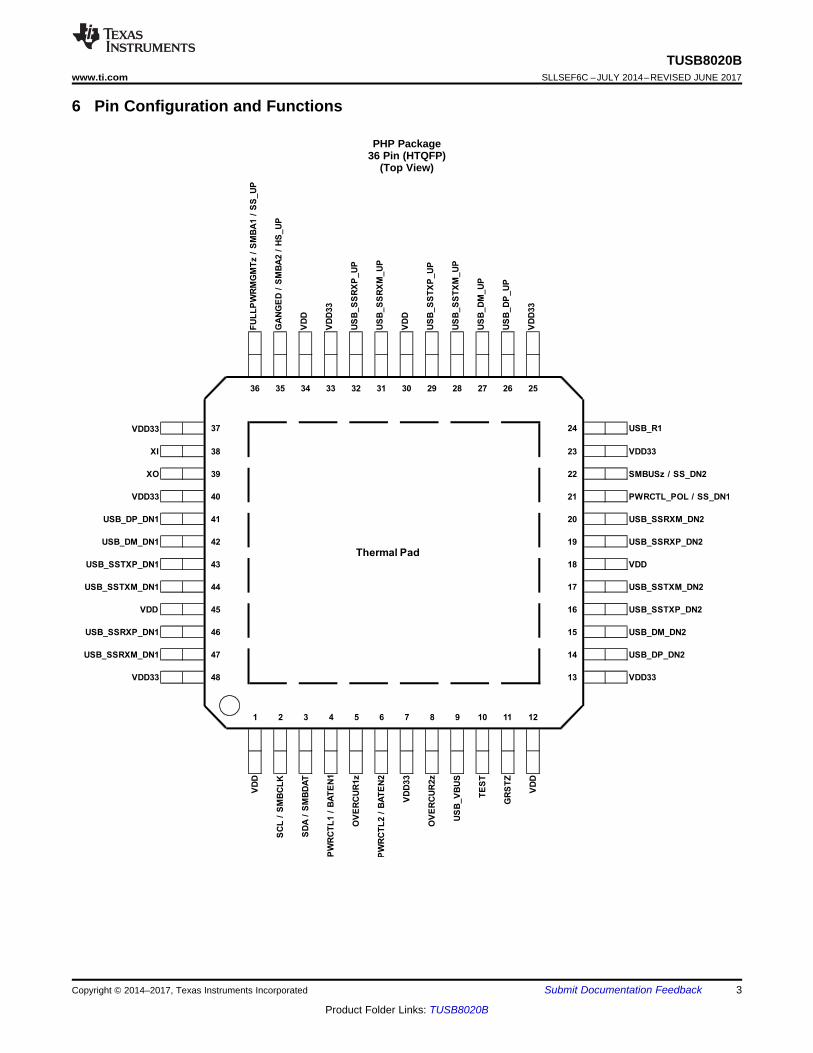
36 35 34 33 32 31 30 29 28 27 26 25
VDD33 37 24 USB_R1
XI 38 23 VDD33
XO 39 22 SMBUSz / SS_DN2
VDD33 40 21 PWRCTL_POL / SS_DN1
USB_DP_DN1 41 20 USB_SSRXM_DN2
USB_DM_DN1 42 19 USB_SSRXP_DN2
USB_SSTXP_DN1 43 18 VDD
USB_SSTXM_DN1 44 17 USB_SSTXM_DN2
VDD 45 16 USB_SSTXP_DN2
USB_SSRXP_DN1 46 15 USB_DM_DN2
USB_SSRXM_DN1 47 14 USB_DP_DN2
VDD33 48 13 VDD33
1 2 3 4 5 6 7 8 9 10 11 12
VD
D
SC
L/
SM
BC
LK
SD
A/
SM
BD
AT
PW
RC
TL
1/
BA
TE
N1
OV
ER
CU
R1z
PW
RC
TL
2/
BA
TE
N2
VD
D33
OV
ER
CU
R2z
US
B_V
BU
S
TE
ST
GR
ST
Z
VD
D
Thermal Pad
3
TUSB8020Bwww.ti.com SLLSEF6C –JULY 2014–REVISED JUNE 2017
Product Folder Links: TUSB8020B
Submit Documentation FeedbackCopyright © 2014–2017, Texas Instruments Incorporated
6 Pin Configuration and Functions
PHP Package36 Pin (HTQFP)
(Top View)
4
TUSB8020BSLLSEF6C –JULY 2014–REVISED JUNE 2017 www.ti.com
Product Folder Links: TUSB8020B
Submit Documentation Feedback Copyright © 2014–2017, Texas Instruments Incorporated
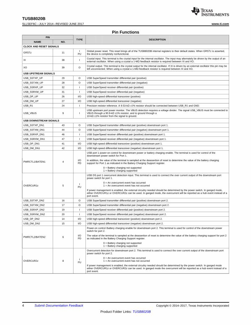
Pin FunctionsPIN
TYPE DESCRIPTIONNAME NO.
CLOCK AND RESET SIGNALS
GRSTz 11 IPU
Global power reset. This reset brings all of the TUSB8020B internal registers to their default states. When GRSTz is asserted,the device is completely nonfunctional.
XI 38 I Crystal input. This terminal is the crystal input for the internal oscillator. The input may alternately be driven by the output of anexternal oscillator. When using a crystal a 1-MΩ feedback resistor is required between XI and XO.
XO 39 O Crystal output. This terminal is the crystal output for the internal oscillator. If XI is driven by an external oscillator this pin may beleft unconnected. When using a crystal a 1-MΩ feedback resistor is required between XI and XO.
USB UPSTREAM SIGNALS
USB_SSTXP_UP 29 O USB SuperSpeed transmitter differential pair (positive)
USB_SSTXM_UP 28 O USB SuperSpeed transmitter differential pair (negative)
USB_SSRXP_UP 32 I USB SuperSpeed receiver differential pair (positive)
USB_SSRXM_UP 31 I USB SuperSpeed receiver differential pair (negative)
USB_DP_UP 26 I/O USB high-speed differential transceiver (positive)
USB_DM_UP 27 I/O USB high-speed differential transceiver (negative)
USB_R1 24 I Precision resistor reference. A 9.53-kΩ ±1% resistor should be connected between USB_R1 and GND.
USB_VBUS 9 IUSB upstream port power monitor. The VBUS detection requires a voltage divider. The signal USB_VBUS must be connected toVBUS through a 90.9-kΩ ±1% resistor, and to ground through a10-kΩ ±1% resistor from the signal to ground.
USB DOWNSTREAM SIGNALS
USB_SSTXP_DN1 43 O USB SuperSpeed transmitter differential pair (positive) downstream port 1.
USB_SSTXM_DN1 44 O USB SuperSpeed transmitter differential pair (negative) downstream port 1.
USB_SSRXP_DN1 46 I USB SuperSpeed receiver differential pair (positive) downstream port 1.
USB_SSRXM_DN1 47 I USB SuperSpeed receiver differential pair (negative) downstream port 1.
USB_DP_DN1 41 I/O USB high-speed differential transceiver (positive) downstream port 1.
USB_DM_DN1 42 I/O USB high-speed differential transceiver (negative) downstream port 1.
PWRCTL1/BATEN1 4 I/OPD
USB port 1 power-on control for downstream power or battery charging enable. The terminal is used for control of thedownstream power switch for Port 1.
In addition, the value of the terminal is sampled at the deassertion of reset to determine the value of the battery chargingsupport for Port 1 as indicated in the Battery Charging Support register.
0 = Battery charging not supported1 = Battery charging supported
OVERCUR1z 5 IPU
USB DS port 1 overcurrent detection input. This terminal is used to connect the over current output of the downstream portpower switch for port 1.
0 = An overcurrent event has occurred1 = An overcurrent event has not occurred
If power management is enabled, the external circuitry needed should be determined by the power switch. In ganged mode,either OVERCUR1z or OVERCUR2z can be used. In ganged mode, the overcurrent will be reported as a hub event instead of aport event.
USB_SSTXP_DN2 16 O USB SuperSpeed transmitter differential pair (positive) downstream port 2.
USB_SSTXM_DN2 17 O USB SuperSpeed transmitter differential pair (negative) downstream port 2.
USB_SSRXP_DN2 19 I USB SuperSpeed receiver differential pair (positive) downstream port 2.
USB_SSRXM_DN2 20 I USB SuperSpeed receiver differential pair (negative) downstream port 2.
USB_DP_DN2 14 I/O USB high-speed differential transceiver (positive) downstream port 2.
USB_DM_DN2 15 I/O USB high-speed differential transceiver (negative) downstream port 2.
PWRCTL2/BATEN2 6 I/OPD
Power-on control /battery charging enable for downstream port 2. This terminal is used for control of the downstream powerswitch for port 2.
The value of the terminal is sampled at the deassertion of reset to determine the value of the battery charging support for port 2as indicated in the Battery Charging Support register.
0 = Battery charging not supported1 = Battery charging supported
OVERCUR2z 8 IPU
Overcurrent detection for downstream port 2. This terminal is used to connect the over current output of the downstream portpower switch for port 2.
0 = An overcurrent event has occurred1 = An overcurrent event has not occurred
If power management is enabled, the external circuitry needed should be determined by the power switch. In ganged modeeither OVERCUR1z or OVERCUR2z can be used. In ganged mode the overcurrent will be reported as a hub event instead of aport event.
5
TUSB8020Bwww.ti.com SLLSEF6C –JULY 2014–REVISED JUNE 2017
Product Folder Links: TUSB8020B
Submit Documentation FeedbackCopyright © 2014–2017, Texas Instruments Incorporated
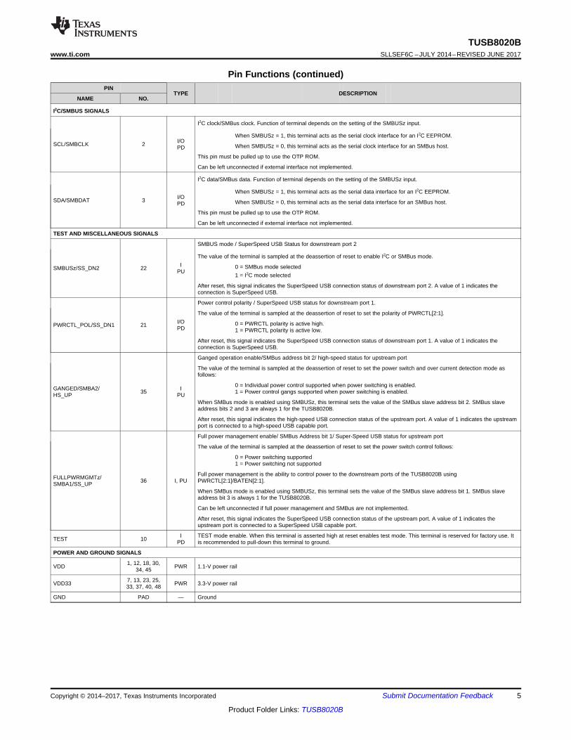
Pin Functions (continued)PIN
TYPE DESCRIPTIONNAME NO.
I2C/SMBUS SIGNALS
SCL/SMBCLK 2 I/OPD
I2C clock/SMBus clock. Function of terminal depends on the setting of the SMBUSz input.
When SMBUSz = 1, this terminal acts as the serial clock interface for an I2C EEPROM.
When SMBUSz = 0, this terminal acts as the serial clock interface for an SMBus host.
This pin must be pulled up to use the OTP ROM.
Can be left unconnected if external interface not implemented.
SDA/SMBDAT 3 I/OPD
I2C data/SMBus data. Function of terminal depends on the setting of the SMBUSz input.
When SMBUSz = 1, this terminal acts as the serial data interface for an I2C EEPROM.
When SMBUSz = 0, this terminal acts as the serial data interface for an SMBus host.
This pin must be pulled up to use the OTP ROM.
Can be left unconnected if external interface not implemented.
TEST AND MISCELLANEOUS SIGNALS
SMBUSz/SS_DN2 22 IPU
SMBUS mode / SuperSpeed USB Status for downstream port 2
The value of the terminal is sampled at the deassertion of reset to enable I2C or SMBus mode.
0 = SMBus mode selected1 = I2C mode selected
After reset, this signal indicates the SuperSpeed USB connection status of downstream port 2. A value of 1 indicates theconnection is SuperSpeed USB.
PWRCTL_POL/SS_DN1 21 I/OPD
Power control polarity / SuperSpeed USB status for downstream port 1.
The value of the terminal is sampled at the deassertion of reset to set the polarity of PWRCTL[2:1].
0 = PWRCTL polarity is active high.1 = PWRCTL polarity is active low.
After reset, this signal indicates the SuperSpeed USB connection status of downstream port 1. A value of 1 indicates theconnection is SuperSpeed USB.
GANGED/SMBA2/HS_UP 35 I
PU
Ganged operation enable/SMBus address bit 2/ high-speed status for upstream port
The value of the terminal is sampled at the deassertion of reset to set the power switch and over current detection mode asfollows:
0 = Individual power control supported when power switching is enabled.1 = Power control gangs supported when power switching is enabled.
When SMBus mode is enabled using SMBUSz, this terminal sets the value of the SMBus slave address bit 2. SMBus slaveaddress bits 2 and 3 are always 1 for the TUSB8020B.
After reset, this signal indicates the high-speed USB connection status of the upstream port. A value of 1 indicates the upstreamport is connected to a high-speed USB capable port.
FULLPWRMGMTz/SMBA1/SS_UP 36 I, PU
Full power management enable/ SMBus Address bit 1/ Super-Speed USB status for upstream port
The value of the terminal is sampled at the deassertion of reset to set the power switch control follows:
0 = Power switching supported1 = Power switching not supported
Full power management is the ability to control power to the downstream ports of the TUSB8020B usingPWRCTL[2:1]/BATEN[2:1].
When SMBus mode is enabled using SMBUSz, this terminal sets the value of the SMBus slave address bit 1. SMBus slaveaddress bit 3 is always 1 for the TUSB8020B.
Can be left unconnected if full power management and SMBus are not implemented.
After reset, this signal indicates the SuperSpeed USB connection status of the upstream port. A value of 1 indicates theupstream port is connected to a SuperSpeed USB capable port.
TEST 10 IPD
TEST mode enable. When this terminal is asserted high at reset enables test mode. This terminal is reserved for factory use. Itis recommended to pull-down this terminal to ground.
POWER AND GROUND SIGNALS
VDD 1, 12, 18, 30,34, 45 PWR 1.1-V power rail
VDD33 7, 13, 23, 25,33, 37, 40, 48 PWR 3.3-V power rail
GND PAD — Ground
6
TUSB8020BSLLSEF6C –JULY 2014–REVISED JUNE 2017 www.ti.com
Product Folder Links: TUSB8020B
Submit Documentation Feedback Copyright © 2014–2017, Texas Instruments Incorporated
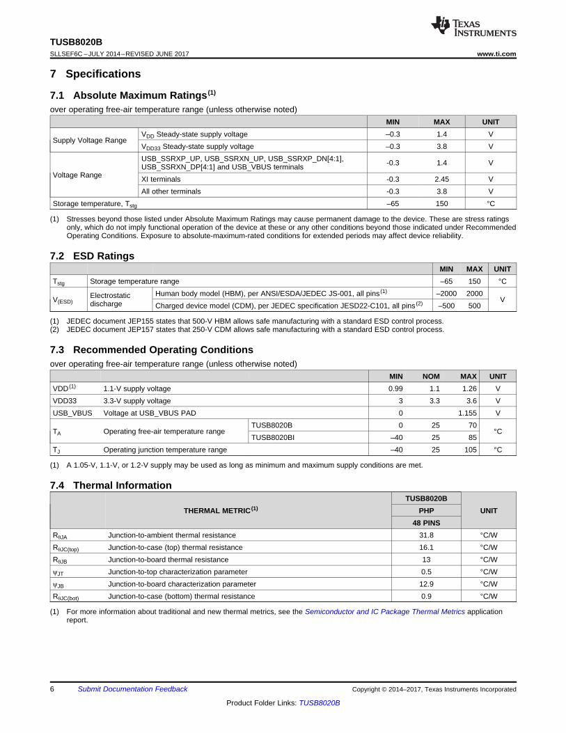
(1) Stresses beyond those listed under Absolute Maximum Ratings may cause permanent damage to the device. These are stress ratingsonly, which do not imply functional operation of the device at these or any other conditions beyond those indicated under RecommendedOperating Conditions. Exposure to absolute-maximum-rated conditions for extended periods may affect device reliability.
7 Specifications
7.1 Absolute Maximum Ratings (1)
over operating free-air temperature range (unless otherwise noted)MIN MAX UNIT
Supply Voltage RangeVDD Steady-state supply voltage –0.3 1.4 VVDD33 Steady-state supply voltage –0.3 3.8 V
Voltage Range
USB_SSRXP_UP, USB_SSRXN_UP, USB_SSRXP_DN[4:1],USB_SSRXN_DP[4:1] and USB_VBUS terminals -0.3 1.4 V
XI terminals -0.3 2.45 VAll other terminals -0.3 3.8 V
Storage temperature, Tstg –65 150 °C
(1) JEDEC document JEP155 states that 500-V HBM allows safe manufacturing with a standard ESD control process.(2) JEDEC document JEP157 states that 250-V CDM allows safe manufacturing with a standard ESD control process.
7.2 ESD RatingsMIN MAX UNIT
Tstg Storage temperature range –65 150 °C
V(ESD)Electrostaticdischarge
Human body model (HBM), per ANSI/ESDA/JEDEC JS-001, all pins (1) –2000 2000V
Charged device model (CDM), per JEDEC specification JESD22-C101, all pins (2) –500 500
(1) A 1.05-V, 1.1-V, or 1.2-V supply may be used as long as minimum and maximum supply conditions are met.
7.3 Recommended Operating Conditionsover operating free-air temperature range (unless otherwise noted)
MIN NOM MAX UNITVDD (1) 1.1-V supply voltage 0.99 1.1 1.26 VVDD33 3.3-V supply voltage 3 3.3 3.6 VUSB_VBUS Voltage at USB_VBUS PAD 0 1.155 V
TA Operating free-air temperature rangeTUSB8020B 0 25 70
°CTUSB8020BI –40 25 85
TJ Operating junction temperature range –40 25 105 °C
(1) For more information about traditional and new thermal metrics, see the Semiconductor and IC Package Thermal Metrics applicationreport.
7.4 Thermal Information
THERMAL METRIC (1)TUSB8020B
UNITPHP48 PINS
RθJA Junction-to-ambient thermal resistance 31.8 °C/WRθJC(top) Junction-to-case (top) thermal resistance 16.1 °C/WRθJB Junction-to-board thermal resistance 13 °C/WψJT Junction-to-top characterization parameter 0.5 °C/WψJB Junction-to-board characterization parameter 12.9 °C/WRθJC(bot) Junction-to-case (bottom) thermal resistance 0.9 °C/W
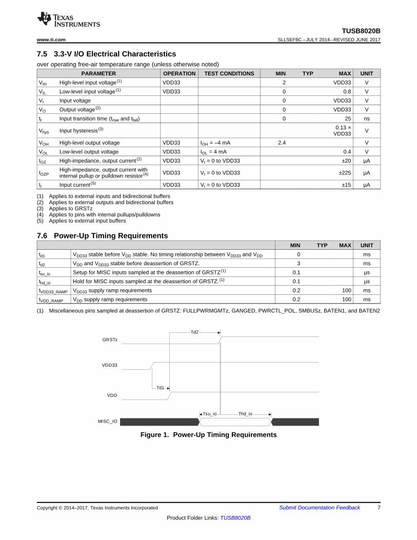
Thd_io Tsu_io
Td1
Td2
GRSTz
VDD33
VDD
MISC_IO
7
TUSB8020Bwww.ti.com SLLSEF6C –JULY 2014–REVISED JUNE 2017
Product Folder Links: TUSB8020B
Submit Documentation FeedbackCopyright © 2014–2017, Texas Instruments Incorporated
(1) Applies to external inputs and bidirectional buffers(2) Applies to external outputs and bidirectional buffers(3) Applies to GRSTz(4) Applies to pins with internal pullups/pulldowns(5) Applies to external input buffers
7.5 3.3-V I/O Electrical Characteristicsover operating free-air temperature range (unless otherwise noted)
PARAMETER OPERATION TEST CONDITIONS MIN TYP MAX UNITVIH High-level input voltage (1) VDD33 2 VDD33 VVIL Low-level input voltage (1) VDD33 0 0.8 VVI Input voltage 0 VDD33 VVO Output voltage (2) 0 VDD33 Vtt Input transition time (trise and tfall) 0 25 ns
Vhys Input hysteresis (3) 0.13 ×VDD33 V
VOH High-level output voltage VDD33 IOH = –4 mA 2.4 VVOL Low-level output voltage VDD33 IOL = 4 mA 0.4 VIOZ High-impedance, output current (2) VDD33 VI = 0 to VDD33 ±20 µA
IOZPHigh-impedance, output current withinternal pullup or pulldown resistor (4) VDD33 VI = 0 to VDD33 ±225 µA
II Input current (5) VDD33 VI = 0 to VDD33 ±15 µA
(1) Miscellaneous pins sampled at deassertion of GRSTZ: FULLPWRMGMTz, GANGED, PWRCTL_POL, SMBUSz, BATEN1, and BATEN2
7.6 Power-Up Timing RequirementsMIN TYP MAX UNIT
td1 VDD33 stable before VDD stable. No timing relationship between VDD33 and VDD 0 mstd2 VDD and VDD33 stable before deassertion of GRSTZ. 3 mstsu_io Setup for MISC inputs sampled at the deassertion of GRSTZ (1) 0.1 µsthd_io Hold for MISC inputs sampled at the deassertion of GRSTZ. (1) 0.1 µstVDD33_RAMP VDD33 supply ramp requirements 0.2 100 mstVDD_RAMP VDD supply ramp requirements 0.2 100 ms
Figure 1. Power-Up Timing Requirements
8
TUSB8020BSLLSEF6C –JULY 2014–REVISED JUNE 2017 www.ti.com
Product Folder Links: TUSB8020B
Submit Documentation Feedback Copyright © 2014–2017, Texas Instruments Incorporated
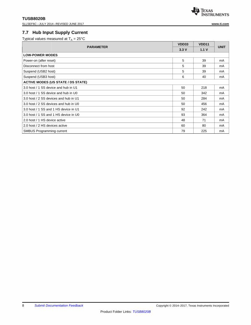
7.7 Hub Input Supply CurrentTypical values measured at TA = 25°C
PARAMETERVDD33 VDD11
UNIT3.3 V 1.1 V
LOW-POWER MODESPower-on (after reset) 5 39 mADisconnect from host 5 39 mASuspend (USB2 host) 5 39 mASuspend (USB3 host) 6 40 mAACTIVE MODES (US STATE / DS STATE)3.0 host / 1 SS device and hub in U1 50 218 mA3.0 host / 1 SS device and hub in U0 50 342 mA3.0 host / 2 SS devices and hub in U1 50 284 mA3.0 host / 2 SS devices and hub in U0 50 456 mA3.0 host / 1 SS and 1 HS device in U1 92 242 mA3.0 host / 1 SS and 1 HS device in U0 93 364 mA2.0 host / 1 HS device active 48 71 mA2.0 host / 2 HS devices active 60 80 mASMBUS Programming current 79 225 mA
VBUS
Detect
SuperSpeed HubUSB 2.0 Hub
US
B_
DP
_U
P
US
B_
SS
RX
P_
UP
US
B_
SS
RX
M_
UP
US
B_
SS
TX
P_
UP
US
B_
SS
TX
M_
UP
US
B_
DM
_U
P
US
B_
SS
RX
P_
DN
1U
SB
_S
SR
XM
_D
N1
US
B_
SS
TX
P_
DN
1U
SB
_S
ST
XM
_D
N1
US
B_
SS
RX
P_
DN
2U
SB
_S
SR
XM
_D
N2
US
B_
SS
TX
P_
DN
2U
SB
_S
ST
XM
_D
N2
US
B_
DP
_D
N1
US
B_
DM
_D
N1
US
B_
DP
_D
N2
US
B_
DM
_D
N2
Oscilator
US
B_
R1
US
B_
VB
US
XI
XO
Clock
and
Reset
Distribution
Control
Registers
GPIO
I2C
SMBUS
Power
Distribution
VDD33
VSS
GRSTn
SCL/SMBCLK
SDA/SMDAT
SMBUSz/SS_DN2
PWRCTL1/BATEN1
OVERCUR1z
PWRCTL2/BATEN2
OVERCUR2z
PWRCTL_POL/SS_DN1
GANGED/SMBA2/HS_UPFULLPWRMGMTz/SMBA1/SS_UP
VDD
TEST
Copyright © 2017, Texas Instruments Incorporated
9
TUSB8020Bwww.ti.com SLLSEF6C –JULY 2014–REVISED JUNE 2017
Product Folder Links: TUSB8020B
Submit Documentation FeedbackCopyright © 2014–2017, Texas Instruments Incorporated
8 Detailed Description
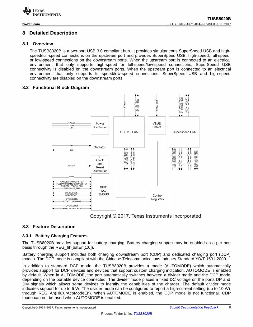
8.1 OverviewThe TUSB8020B is a two-port USB 3.0 compliant hub. It provides simultaneous SuperSpeed USB and high-speed/full-speed connections on the upstream port and provides SuperSpeed USB, high-speed, full-speed,or low-speed connections on the downstream ports. When the upstream port is connected to an electricalenvironment that only supports high-speed or full-speed/low-speed connections, SuperSpeed USBconnectivity is disabled on the downstream ports. When the upstream port is connected to an electricalenvironment that only supports full-speed/low-speed connections, SuperSpeed USB and high-speedconnectivity are disabled on the downstream ports.
8.2 Functional Block Diagram
8.3 Feature Description
8.3.1 Battery Charging FeaturesThe TUSB8020B provides support for battery charging. Battery charging support may be enabled on a per portbasis through the REG_6h(batEn[1:0]).
Battery charging support includes both charging downstream port (CDP) and dedicated charging port (DCP)modes. The DCP mode is compliant with the Chinese Telecommunications Industry Standard YD/T 1591-2009.
In addition to standard DCP mode, the TUSB8020B provides a mode (AUTOMODE) which automaticallyprovides support for DCP devices and devices that support custom charging indication. AUTOMODE is enabledby default. When in AUTOMODE, the port automatically switches between a divider mode and the DCP modedepending on the portable device connected. The divider mode places a fixed DC voltage on the ports DP andDM signals which allows some devices to identify the capabilities of the charger. The default divider modeindicates support for up to 5 W. The divider mode can be configured to report a high-current setting (up to 10 W)through REG_Ah(HiCurAcpModeEn). When AUTOMODE is enabled, the CDP mode is not functional. CDPmode can not be used when AUTOMODE is enabled.
10
TUSB8020BSLLSEF6C –JULY 2014–REVISED JUNE 2017 www.ti.com
Product Folder Links: TUSB8020B
Submit Documentation Feedback Copyright © 2014–2017, Texas Instruments Incorporated
Feature Description (continued)The battery charging mode for each port depends on the state of Reg_6h(batEn[n]), the status of the VBUSinput, and the state of REG_Ah(autoModeEnz) upstream port, as identified in Table 1. Battery charging can alsobe enabled through the PWRCTL1/BATEN1 and PWRCTL2/BATEN2 pins.
(1) Auto-mode automatically selects divider-mode or DCP mode.(2) Divider mode can be configured for high-current mode through register or OTP settings.(3) USB device is USB Battery Charging Specification Revision 1.2 Compliant(4) USB device is Chinese Telecommunications Industry Standard YD/T 1591-2009
Table 1. TUSB8020B Battery Charging Modes
batEn[n] VBUS autoModeEnz BC Mode Port x(x = n + 1)
0 Don’t care Don’t care Don’t care
1<4 V
0 Automode (1) (2)
1 DCP (3) (4)
>4 V 1 CDP (3)
8.3.2 USB Power ManagementThe TUSB8020B can be configured for power switched applications using either per-port or ganged power-enable controls and over-current status inputs.
Power switch support is enabled by REG_5h(fullPwrMgmtz) and the per-port or ganged mode is configured byREG_5h(ganged). It can also be enabled through the FULLPWRMGMTz pin. Also ganged or individual controlcan be controlled by the GANGED pin.
The TUSB8020B supports both active-high and active-low power-enable controls. The PWRCTL[2:1] polarity isconfigured by REG_Ah(pwrctlPol). The polarity can also be configured by the PWRCTL_POL pin.
8.3.3 One-Time Programmable (OTP) ConfigurationThe TUSB8020B allows device configuration through OTP non-volatile memory (OTP). The programming of theOTP is supported using vendor-defined USB device requests. For details using the OTP features, contact your TIrepresentative.
Table 2 provides a list features which may be configured using the OTP. The bit field section in Table 2 showswhich features can be controlled by OTP ROM. The bits not listed in the table are not accessible by the OTPROM.
Table 2. OTP Configurable FeaturesCONFIGURATION REGISTER OFFSET BIT FIELD DESCRIPTION
REG_01h [7:0] Vendor ID LSBREG_02h [7:0] Vendor ID MSBREG_03h [7:0] Product ID LSBREG_04h [7:0] Product ID MSB
REG_07h [0]
Port removable configuration for downstream ports 1. OTP configuration isinverse of rmbl[1:0], that is:1 = Not removable0 = Removable
REG_07h [1]
Port removable configuration for downstream ports 2. OTP configuration isinverse of rmbl[1:0], that is:1 = Not removable0 = Removable
REG_0Ah [1] Automode enableREG_0Ah [4] High-current divider mode enable.REG_F2h [3:1] USB power switch power-on delay.
Copyright © 2017, Texas Instruments Incorporated
11
TUSB8020Bwww.ti.com SLLSEF6C –JULY 2014–REVISED JUNE 2017
Product Folder Links: TUSB8020B
Submit Documentation FeedbackCopyright © 2014–2017, Texas Instruments Incorporated
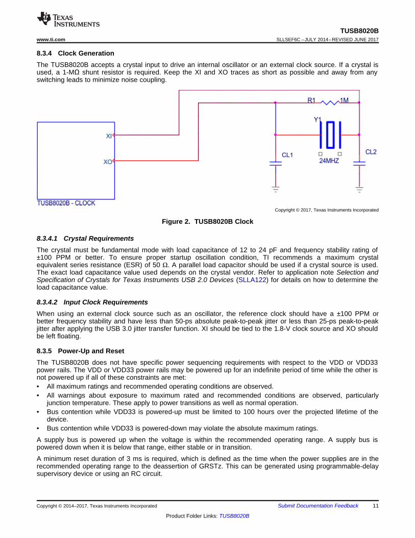
8.3.4 Clock GenerationThe TUSB8020B accepts a crystal input to drive an internal oscillator or an external clock source. If a crystal isused, a 1-MΩ shunt resistor is required. Keep the XI and XO traces as short as possible and away from anyswitching leads to minimize noise coupling.
Figure 2. TUSB8020B Clock
8.3.4.1 Crystal RequirementsThe crystal must be fundamental mode with load capacitance of 12 to 24 pF and frequency stability rating of±100 PPM or better. To ensure proper startup oscillation condition, TI recommends a maximum crystalequivalent series resistance (ESR) of 50 Ω. A parallel load capacitor should be used if a crystal source is used.The exact load capacitance value used depends on the crystal vendor. Refer to application note Selection andSpecification of Crystals for Texas Instruments USB 2.0 Devices (SLLA122) for details on how to determine theload capacitance value.
8.3.4.2 Input Clock RequirementsWhen using an external clock source such as an oscillator, the reference clock should have a ±100 PPM orbetter frequency stability and have less than 50-ps absolute peak-to-peak jitter or less than 25-ps peak-to-peakjitter after applying the USB 3.0 jitter transfer function. XI should be tied to the 1.8-V clock source and XO shouldbe left floating.
8.3.5 Power-Up and ResetThe TUSB8020B does not have specific power sequencing requirements with respect to the VDD or VDD33power rails. The VDD or VDD33 power rails may be powered up for an indefinite period of time while the other isnot powered up if all of these constraints are met:• All maximum ratings and recommended operating conditions are observed.• All warnings about exposure to maximum rated and recommended conditions are observed, particularly
junction temperature. These apply to power transitions as well as normal operation.• Bus contention while VDD33 is powered-up must be limited to 100 hours over the projected lifetime of the
device.• Bus contention while VDD33 is powered-down may violate the absolute maximum ratings.
A supply bus is powered up when the voltage is within the recommended operating range. A supply bus ispowered down when it is below that range, either stable or in transition.
A minimum reset duration of 3 ms is required, which is defined as the time when the power supplies are in therecommended operating range to the deassertion of GRSTz. This can be generated using programmable-delaysupervisory device or using an RC circuit.
12
TUSB8020BSLLSEF6C –JULY 2014–REVISED JUNE 2017 www.ti.com
Product Folder Links: TUSB8020B
Submit Documentation Feedback Copyright © 2014–2017, Texas Instruments Incorporated
8.4 Device Functional Modes
8.4.1 External Configuration InterfaceThe TUSB8020B supports a serial interface for configuration register access. The device may be configured byan attached I2C EEPROM or accessed as a slave by a SMBus-capable host controller. The external interface isenabled when both the SCL/SMBCLK and SDA/SMBDAT terminals are pulled up to 3.3 V at the deassertion ofreset. The mode, I2C master, or SMBus slave is determined by the state of SMBUSz/SS_DN2 terminal at reset.
8.4.2 I2C EEPROM OperationThe TUSB8020B supports a single-master, standard mode (100 kbit/s) connection to a dedicated I2C EEPROMwhen the I2C interface mode is enabled. In I2C mode, the TUSB8020B reads the contents of the EEPROM at busaddress 1010000b using 7-bit addressing starting at address 0.
If the value of the EEPROM contents at byte 00h equals 55h, the TUSB8020B loads the configuration registersaccording to the EEPROM map. If the first byte is not 55h, the TUSB8020B exits the I2C mode and continuesexecution with the default values in the configuration registers. The hub will not connect on the upstream portuntil the configuration is completed. If the TUSB8020B detects an unprogrammed EEPROM (value other than55h), it enters programming mode and a programming endpoint within the hub is enabled.
Note, the bytes located above offset Ah are optional. The requirement for data in those addresses depends onthe options configured in the Device Configuration, Phy Custom Configuration, and Device Configuration 2registers.
For details on I2C operation, refer to the UM10204 I2C-bus Specification and User Manual.
8.4.3 SMBus Slave OperationWhen the SMBus interface mode is enabled, the TUSB8020B supports read block and write block protocols as aslave-only SMBus device.
The TUSB8020B slave address is 1000 1xyz, where:• x is the state of GANGED/SMBA2/HS_UP terminal at reset• y is the state of FULLPWRMGMTz/SMBA1/SS_UP terminal at reset• z is the read/write bit; 1 = read access, 0 = write access.
If the TUSB8020B is addressed by a host using an unsupported protocol, it does not respond. The TUSB8020Bwaits indefinitely for configuration by the SMBus host and does not connect on the upstream port until theSMBus host indicates configuration is complete by clearing the CFG_ACTIVE bit.
For details on SMBus requirements, refer to the System Management Bus Specification.
NOTEDuring the SMBUS configuration the hub may draw an extra current, this extra currentconsumption will end as soon as the CFG_ACTIVE bit is cleared. For more information,see Hub Input Supply Current in this datasheet.
13
TUSB8020Bwww.ti.com SLLSEF6C –JULY 2014–REVISED JUNE 2017
Product Folder Links: TUSB8020B
Submit Documentation FeedbackCopyright © 2014–2017, Texas Instruments Incorporated
8.5 Register Maps
8.5.1 Configuration RegistersThe internal configuration registers are accessed on byte boundaries. The configuration register values areloaded with defaults but can be overwritten when the TUSB8020B is in I2C or SMBus mode.
Table 3. TUSB8020B Register MapBYTE ADDRESS CONTENTS EEPROM CONFIGURABLE
00h ROM Signature Register No01h Vendor ID LSB Yes02h Vendor ID MSB Yes03h Product ID LSB Yes04h Product ID MSB Yes05h Device Configuration Register Yes06h Battery Charging Support Register Yes07h Device Removable Configuration Register Yes08h Port Used Configuration Register Yes09h Reserved Yes, program to 00h0Ah Device Configuration Register 2 Yes
0Bh to 0Fh Reserved10h to 1Fh UUID Byte [15:0] No20h to 21h LangID Byte [1:0] Yes, if customStrings is set
22h Serial Number String Length Yes, if customSerNum is set23h Manufacturer String Length Yes, if customStrings is set24h Product String Length Yes, if customStrings is set
25h to 2Fh Reserved Yes30h to 4Fh Serial Number String Byte [31:0] Yes, if customSerNum is set50h to 8Fh Manufacturer String Byte [63:0] Yes, if customStrings is set90h to CFh Product String Byte [63:0] Yes, if customStrings is setD0 to DFh Reserved No
F0h Additional Feature Configuration Register YesF1h Reserved YesF2h Charging Port Control Register Yes
F3 to F7h Reserved NoF8h Device Status and Command Register No
F9 to FFh Reserved No
14
TUSB8020BSLLSEF6C –JULY 2014–REVISED JUNE 2017 www.ti.com
Product Folder Links: TUSB8020B
Submit Documentation Feedback Copyright © 2014–2017, Texas Instruments Incorporated
8.5.1.1 ROM Signature Register (offset = 0h) [reset = 0h]
Figure 3. Register Offset 0h
7 6 5 4 3 2 1 00 0 0 0 0 0 0 0
R/W R/W R/W R/W R/W R/W R/W R/WLEGEND: R/W = Read/Write; R = Read only; –n = value after reset
Table 4. ROM Signature RegisterBit Field Type Reset Description
7:0 romSignature R/W 0h
ROM Signature Register. This register is used by the TUSB8020B in I2C mode tovalidate the attached EEPROM has been programmed. The first byte of theEEPROM is compared to the mask 55h and if not a match, the TUSB8020B abortsthe EEPROM load and executes with the register defaults.
8.5.1.2 Vendor ID LSB Register (offset = 1h) [reset = 51h]
Figure 4. Register Offset 51h
7 6 5 4 3 2 1 00 1 0 1 0 0 0 1
R/W R/W R/W R/W R/W R/W R/W R/WLEGEND: R/W = Read/Write; R = Read only; –n = value after reset
Table 5. Vendor ID LSB RegisterBit Field Type Reset Description
7:0 vendorIdLsb R/W 51h
Vendor ID LSB. Least significant byte of the unique vendor ID assigned by theUSB-IF; the default value of this register is 51h representing the LSB of the TIVendor ID 0451h. The value may be overwritten to indicate a customer vendor ID.This field is read/write unless the OTP ROM VID and OTP ROM PID values arenon-zero. If both values are non-zero, the value when reading this register shallreflect the OTP ROM value.
8.5.1.3 Vendor ID MSB Register (offset = 2h) [reset = 4h]
Figure 5. Register Offset 2h
7 6 5 4 3 2 1 00 0 0 0 0 1 0 0
R/W R/W R/W R/W R/W R/W R/W R/WLEGEND: R/W = Read/Write; R = Read only; –n = value after reset
Table 6. Vendor ID MSB RegisterBit Field Type Reset Description
7:0 vendorIdMsb R/W 4h
Vendor ID MSB. Most significant byte of the unique vendor ID assigned by theUSB-IF; the default value of this register is 04h representing the MSB of the TIVendor ID 0451h. The value may be overwritten to indicate a customer vendor ID.This field is read/write unless the OTP ROM VID and OTP ROM PID values arenon-zero. If both values are non-zero, the value when reading this register shallreflect the OTP ROM value.
15
TUSB8020Bwww.ti.com SLLSEF6C –JULY 2014–REVISED JUNE 2017
Product Folder Links: TUSB8020B
Submit Documentation FeedbackCopyright © 2014–2017, Texas Instruments Incorporated
8.5.1.4 Product ID LSB Register (offset = 3h) [reset = 25h]
Figure 6. Register Offset 3h
7 6 5 4 3 2 1 00 0 1 0 0 1 0 1
R/W R/W R/W R/W R/W R/W R/W R/WLEGEND: R/W = Read/Write; R = Read only; –n = value after reset
Table 7. Product ID LSB RegisterBit Field Type Reset Description
7:0 productIdLsb R/W 25h
Product ID LSB. Least significant byte of the product ID assigned by TI and reported inthe SuperSpeed device descriptor. The default value of this register is 25h representingthe LSB of the SuperSpeed product ID assigned by TI. The value reported in the USB2.0 device descriptor is the value of this register bit wise XORed with 00000010b. Thevalue may be overwritten to indicate a customer product ID.This field is read/write unless the OTP ROM VID and OTP ROM PID values are non-zero. If both values are non-zero, the value when reading this register shall reflect theOTP ROM value.
8.5.1.5 Product ID MSB Register (offset = 4h) [reset = 80h]
Figure 7. Register Offset 4h
7 6 5 4 3 2 1 01 0 0 0 0 0 0 0
R/W R/W R/W R/W R/W R/W R/W R/WLEGEND: R/W = Read/Write; R = Read only; –n = value after reset
Table 8. Bit Descriptions – Product ID MSB RegisterBit Field Type Reset Description
7:0 productIdLsb R/W 80h
Product ID MSB. Most significant byte of the product ID assigned by TI; the defaultvalue of this register is 80h representing the MSB of the product ID assigned by TI. Thevalue may be overwritten to indicate a customer product ID.This field is read/write unless the OTP ROM VID and OTP ROM PID values are non-zero. If both values are non-zero, the value when reading this register will reflect theOTP ROM value.
16
TUSB8020BSLLSEF6C –JULY 2014–REVISED JUNE 2017 www.ti.com
Product Folder Links: TUSB8020B
Submit Documentation Feedback Copyright © 2014–2017, Texas Instruments Incorporated
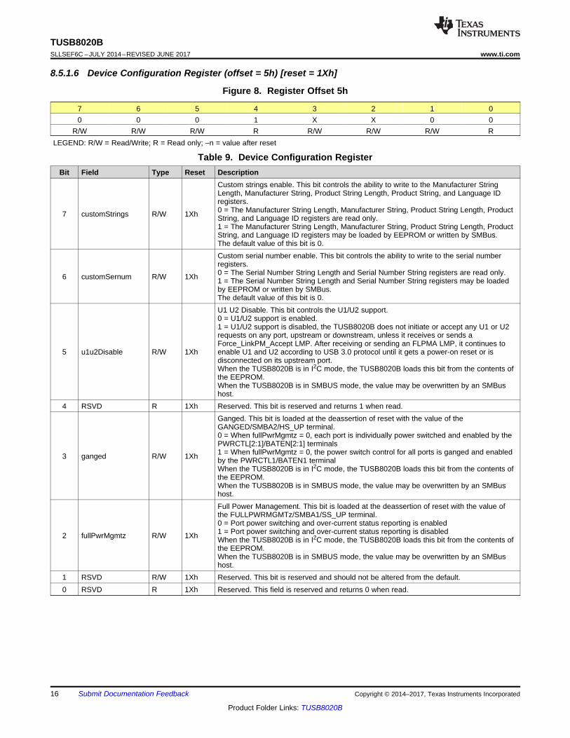
8.5.1.6 Device Configuration Register (offset = 5h) [reset = 1Xh]
Figure 8. Register Offset 5h
7 6 5 4 3 2 1 00 0 0 1 X X 0 0
R/W R/W R/W R R/W R/W R/W RLEGEND: R/W = Read/Write; R = Read only; –n = value after reset
Table 9. Device Configuration RegisterBit Field Type Reset Description
7 customStrings R/W 1Xh
Custom strings enable. This bit controls the ability to write to the Manufacturer StringLength, Manufacturer String, Product String Length, Product String, and Language IDregisters.0 = The Manufacturer String Length, Manufacturer String, Product String Length, ProductString, and Language ID registers are read only.1 = The Manufacturer String Length, Manufacturer String, Product String Length, ProductString, and Language ID registers may be loaded by EEPROM or written by SMBus.The default value of this bit is 0.
6 customSernum R/W 1Xh
Custom serial number enable. This bit controls the ability to write to the serial numberregisters.0 = The Serial Number String Length and Serial Number String registers are read only.1 = The Serial Number String Length and Serial Number String registers may be loadedby EEPROM or written by SMBus.The default value of this bit is 0.
5 u1u2Disable R/W 1Xh
U1 U2 Disable. This bit controls the U1/U2 support.0 = U1/U2 support is enabled.1 = U1/U2 support is disabled, the TUSB8020B does not initiate or accept any U1 or U2requests on any port, upstream or downstream, unless it receives or sends aForce_LinkPM_Accept LMP. After receiving or sending an FLPMA LMP, it continues toenable U1 and U2 according to USB 3.0 protocol until it gets a power-on reset or isdisconnected on its upstream port.When the TUSB8020B is in I2C mode, the TUSB8020B loads this bit from the contents ofthe EEPROM.When the TUSB8020B is in SMBUS mode, the value may be overwritten by an SMBushost.
4 RSVD R 1Xh Reserved. This bit is reserved and returns 1 when read.
3 ganged R/W 1Xh
Ganged. This bit is loaded at the deassertion of reset with the value of theGANGED/SMBA2/HS_UP terminal.0 = When fullPwrMgmtz = 0, each port is individually power switched and enabled by thePWRCTL[2:1]/BATEN[2:1] terminals1 = When fullPwrMgmtz = 0, the power switch control for all ports is ganged and enabledby the PWRCTL1/BATEN1 terminalWhen the TUSB8020B is in I2C mode, the TUSB8020B loads this bit from the contents ofthe EEPROM.When the TUSB8020B is in SMBUS mode, the value may be overwritten by an SMBushost.
2 fullPwrMgmtz R/W 1Xh
Full Power Management. This bit is loaded at the deassertion of reset with the value ofthe FULLPWRMGMTz/SMBA1/SS_UP terminal.0 = Port power switching and over-current status reporting is enabled1 = Port power switching and over-current status reporting is disabledWhen the TUSB8020B is in I2C mode, the TUSB8020B loads this bit from the contents ofthe EEPROM.When the TUSB8020B is in SMBUS mode, the value may be overwritten by an SMBushost.
1 RSVD R/W 1Xh Reserved. This bit is reserved and should not be altered from the default.0 RSVD R 1Xh Reserved. This field is reserved and returns 0 when read.
17
TUSB8020Bwww.ti.com SLLSEF6C –JULY 2014–REVISED JUNE 2017
Product Folder Links: TUSB8020B
Submit Documentation FeedbackCopyright © 2014–2017, Texas Instruments Incorporated
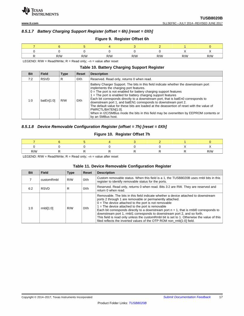
8.5.1.7 Battery Charging Support Register (offset = 6h) [reset = 0Xh]
Figure 9. Register Offset 6h
7 6 5 4 3 2 1 00 0 0 0 0 0 X XR R/W R/W R/W R/W R/W R/W R/W
LEGEND: R/W = Read/Write; R = Read only; –n = value after reset
Table 10. Battery Charging Support RegisterBit Field Type Reset Description7:2 RSVD R 0Xh Reserved. Read only, returns 0 when read.
1:0 batEn[1:0] R/W 0Xh
Battery Charger Support. The bits in this field indicate whether the downstream portimplements the charging port features.0 = The port is not enabled for battery charging support features1 = The port is enabled for battery charging support featuresEach bit corresponds directly to a downstream port, that is batEn0 corresponds todownstream port 1, and batEN1 corresponds to downstream port 2.The default value for these bits are loaded at the deassertion of reset with the value ofPWRCTL/BATEN[1:0].When in I2C/SMBus mode the bits in this field may be overwritten by EEPROM contents orby an SMBus host.
8.5.1.8 Device Removable Configuration Register (offset = 7h) [reset = 0Xh]
Figure 10. Register Offset 7h
7 6 5 4 3 2 1 00 0 0 0 0 0 X X
R/W R R R R R R R/WLEGEND: R/W = Read/Write; R = Read only; –n = value after reset
Table 11. Device Removable Configuration RegisterBit Field Type Reset Description
7 customRmbl R/W 0Xh Custom removable status. When this field is a 1, the TUSB8020B uses rmbl bits in thisregister to identify removable status for the ports.
6:2 RSVD R 0Xh Reserved. Read only, returns 0 when read. Bits 3:2 are RW. They are reserved andreturn 0 when read.
1:0 rmbl[1:0] R/W 0Xh
Removable. The bits in this field indicate whether a device attached to downstreamports 2 through 1 are removable or permanently attached.0 = The device attached to the port is not removable1 = The device attached to the port is removableEach bit corresponds directly to a downstream port n + 1, that is rmbl0 corresponds todownstream port 1, rmbl1 corresponds to downstream port 2, and so forth.This field is read only unless the customRmbl bit is set to 1. Otherwise the value of thisfiled reflects the inverted values of the OTP ROM non_rmb[1:0] field.
18
TUSB8020BSLLSEF6C –JULY 2014–REVISED JUNE 2017 www.ti.com
Product Folder Links: TUSB8020B
Submit Documentation Feedback Copyright © 2014–2017, Texas Instruments Incorporated
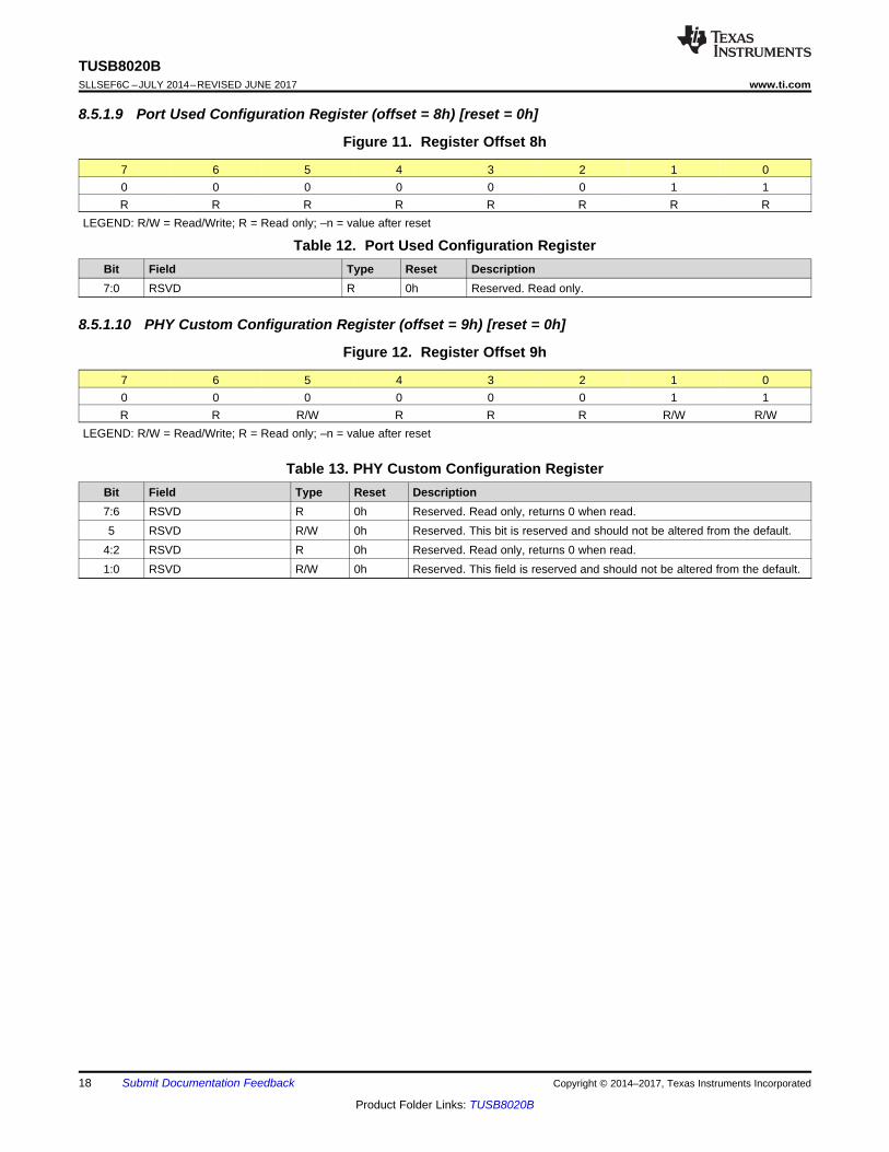
8.5.1.9 Port Used Configuration Register (offset = 8h) [reset = 0h]
Figure 11. Register Offset 8h
7 6 5 4 3 2 1 00 0 0 0 0 0 1 1R R R R R R R R
LEGEND: R/W = Read/Write; R = Read only; –n = value after reset
Table 12. Port Used Configuration RegisterBit Field Type Reset Description7:0 RSVD R 0h Reserved. Read only.
8.5.1.10 PHY Custom Configuration Register (offset = 9h) [reset = 0h]
Figure 12. Register Offset 9h
7 6 5 4 3 2 1 00 0 0 0 0 0 1 1R R R/W R R R R/W R/W
LEGEND: R/W = Read/Write; R = Read only; –n = value after reset
Table 13. PHY Custom Configuration RegisterBit Field Type Reset Description7:6 RSVD R 0h Reserved. Read only, returns 0 when read.5 RSVD R/W 0h Reserved. This bit is reserved and should not be altered from the default.
4:2 RSVD R 0h Reserved. Read only, returns 0 when read.1:0 RSVD R/W 0h Reserved. This field is reserved and should not be altered from the default.
19
TUSB8020Bwww.ti.com SLLSEF6C –JULY 2014–REVISED JUNE 2017
Product Folder Links: TUSB8020B
Submit Documentation FeedbackCopyright © 2014–2017, Texas Instruments Incorporated
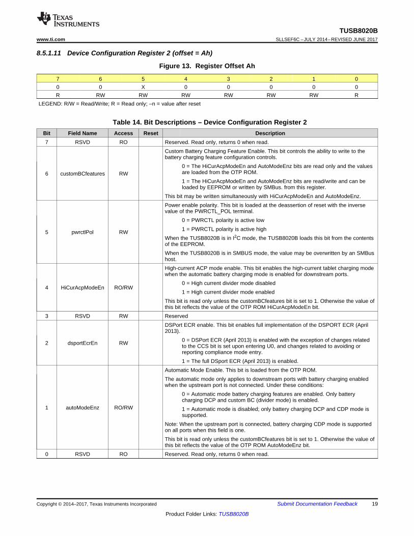
8.5.1.11 Device Configuration Register 2 (offset = Ah)
Figure 13. Register Offset Ah
7 6 5 4 3 2 1 00 0 X 0 0 0 0 0R RW RW RW RW RW RW R
LEGEND: R/W = Read/Write; R = Read only; –n = value after reset
Table 14. Bit Descriptions – Device Configuration Register 2Bit Field Name Access Reset Description7 RSVD RO Reserved. Read only, returns 0 when read.
6 customBCfeatures RW
Custom Battery Charging Feature Enable. This bit controls the ability to write to thebattery charging feature configuration controls.
0 = The HiCurAcpModeEn and AutoModeEnz bits are read only and the valuesare loaded from the OTP ROM.1 = The HiCurAcpModeEn and AutoModeEnz bits are read/write and can beloaded by EEPROM or written by SMBus. from this register.
This bit may be written simultaneously with HiCurAcpModeEn and AutoModeEnz.
5 pwrctlPol RW
Power enable polarity. This bit is loaded at the deassertion of reset with the inversevalue of the PWRCTL_POL terminal.
0 = PWRCTL polarity is active low1 = PWRCTL polarity is active high
When the TUSB8020B is in I2C mode, the TUSB8020B loads this bit from the contentsof the EEPROM.When the TUSB8020B is in SMBUS mode, the value may be overwritten by an SMBushost.
4 HiCurAcpModeEn RO/RW
High-current ACP mode enable. This bit enables the high-current tablet charging modewhen the automatic battery charging mode is enabled for downstream ports.
0 = High current divider mode disabled1 = High current divider mode enabled
This bit is read only unless the customBCfeatures bit is set to 1. Otherwise the value ofthis bit reflects the value of the OTP ROM HiCurAcpModeEn bit.
3 RSVD RW Reserved
2 dsportEcrEn RW
DSPort ECR enable. This bit enables full implementation of the DSPORT ECR (April2013).
0 = DSPort ECR (April 2013) is enabled with the exception of changes relatedto the CCS bit is set upon entering U0, and changes related to avoiding orreporting compliance mode entry.1 = The full DSport ECR (April 2013) is enabled.
1 autoModeEnz RO/RW
Automatic Mode Enable. This bit is loaded from the OTP ROM.The automatic mode only applies to downstream ports with battery charging enabledwhen the upstream port is not connected. Under these conditions:
0 = Automatic mode battery charging features are enabled. Only batterycharging DCP and custom BC (divider mode) is enabled.1 = Automatic mode is disabled; only battery charging DCP and CDP mode issupported.
Note: When the upstream port is connected, battery charging CDP mode is supportedon all ports when this field is one.This bit is read only unless the customBCfeatures bit is set to 1. Otherwise the value ofthis bit reflects the value of the OTP ROM AutoModeEnz bit.
0 RSVD RO Reserved. Read only, returns 0 when read.
20
TUSB8020BSLLSEF6C –JULY 2014–REVISED JUNE 2017 www.ti.com
Product Folder Links: TUSB8020B
Submit Documentation Feedback Copyright © 2014–2017, Texas Instruments Incorporated
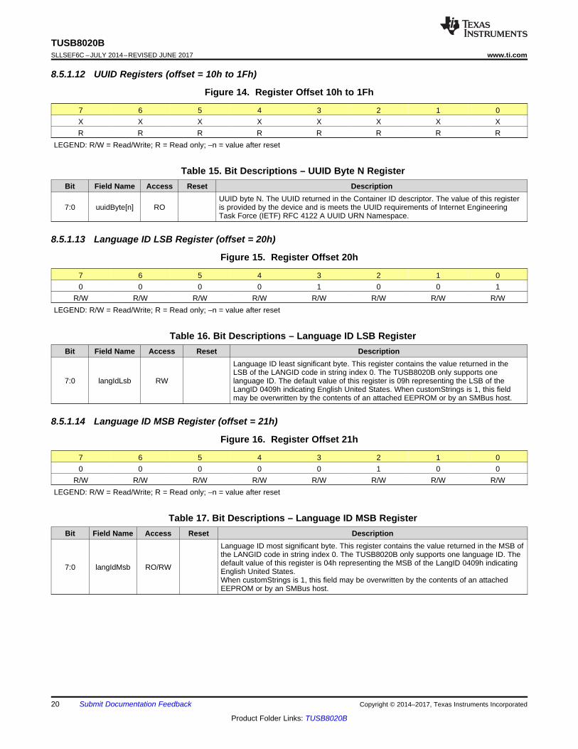
8.5.1.12 UUID Registers (offset = 10h to 1Fh)
Figure 14. Register Offset 10h to 1Fh
7 6 5 4 3 2 1 0X X X X X X X XR R R R R R R R
LEGEND: R/W = Read/Write; R = Read only; –n = value after reset
Table 15. Bit Descriptions – UUID Byte N RegisterBit Field Name Access Reset Description
7:0 uuidByte[n] ROUUID byte N. The UUID returned in the Container ID descriptor. The value of this registeris provided by the device and is meets the UUID requirements of Internet EngineeringTask Force (IETF) RFC 4122 A UUID URN Namespace.
8.5.1.13 Language ID LSB Register (offset = 20h)
Figure 15. Register Offset 20h
7 6 5 4 3 2 1 00 0 0 0 1 0 0 1
R/W R/W R/W R/W R/W R/W R/W R/WLEGEND: R/W = Read/Write; R = Read only; –n = value after reset
Table 16. Bit Descriptions – Language ID LSB RegisterBit Field Name Access Reset Description
7:0 langIdLsb RW
Language ID least significant byte. This register contains the value returned in theLSB of the LANGID code in string index 0. The TUSB8020B only supports onelanguage ID. The default value of this register is 09h representing the LSB of theLangID 0409h indicating English United States. When customStrings is 1, this fieldmay be overwritten by the contents of an attached EEPROM or by an SMBus host.
8.5.1.14 Language ID MSB Register (offset = 21h)
Figure 16. Register Offset 21h
7 6 5 4 3 2 1 00 0 0 0 0 1 0 0
R/W R/W R/W R/W R/W R/W R/W R/WLEGEND: R/W = Read/Write; R = Read only; –n = value after reset
Table 17. Bit Descriptions – Language ID MSB RegisterBit Field Name Access Reset Description
7:0 langIdMsb RO/RW
Language ID most significant byte. This register contains the value returned in the MSB ofthe LANGID code in string index 0. The TUSB8020B only supports one language ID. Thedefault value of this register is 04h representing the MSB of the LangID 0409h indicatingEnglish United States.When customStrings is 1, this field may be overwritten by the contents of an attachedEEPROM or by an SMBus host.
21
TUSB8020Bwww.ti.com SLLSEF6C –JULY 2014–REVISED JUNE 2017
Product Folder Links: TUSB8020B
Submit Documentation FeedbackCopyright © 2014–2017, Texas Instruments Incorporated
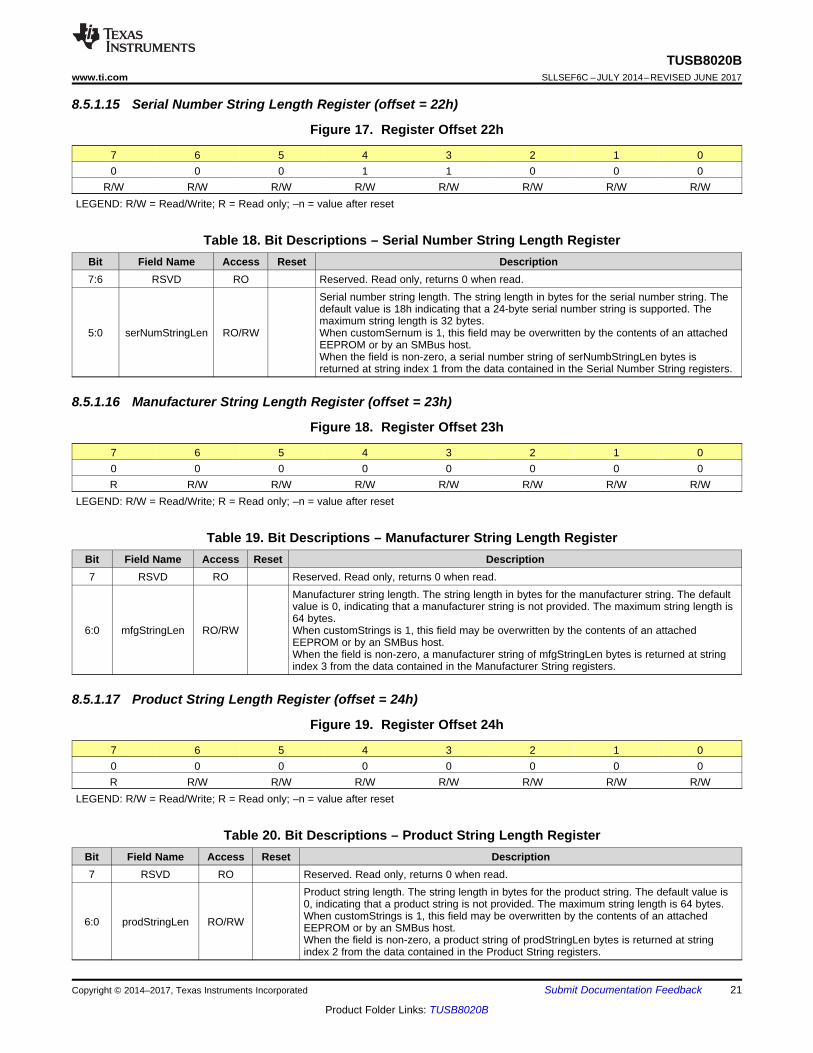
8.5.1.15 Serial Number String Length Register (offset = 22h)
Figure 17. Register Offset 22h
7 6 5 4 3 2 1 00 0 0 1 1 0 0 0
R/W R/W R/W R/W R/W R/W R/W R/WLEGEND: R/W = Read/Write; R = Read only; –n = value after reset
Table 18. Bit Descriptions – Serial Number String Length RegisterBit Field Name Access Reset Description7:6 RSVD RO Reserved. Read only, returns 0 when read.
5:0 serNumStringLen RO/RW
Serial number string length. The string length in bytes for the serial number string. Thedefault value is 18h indicating that a 24-byte serial number string is supported. Themaximum string length is 32 bytes.When customSernum is 1, this field may be overwritten by the contents of an attachedEEPROM or by an SMBus host.When the field is non-zero, a serial number string of serNumbStringLen bytes isreturned at string index 1 from the data contained in the Serial Number String registers.
8.5.1.16 Manufacturer String Length Register (offset = 23h)
Figure 18. Register Offset 23h
7 6 5 4 3 2 1 00 0 0 0 0 0 0 0R R/W R/W R/W R/W R/W R/W R/W
LEGEND: R/W = Read/Write; R = Read only; –n = value after reset
Table 19. Bit Descriptions – Manufacturer String Length RegisterBit Field Name Access Reset Description7 RSVD RO Reserved. Read only, returns 0 when read.
6:0 mfgStringLen RO/RW
Manufacturer string length. The string length in bytes for the manufacturer string. The defaultvalue is 0, indicating that a manufacturer string is not provided. The maximum string length is64 bytes.When customStrings is 1, this field may be overwritten by the contents of an attachedEEPROM or by an SMBus host.When the field is non-zero, a manufacturer string of mfgStringLen bytes is returned at stringindex 3 from the data contained in the Manufacturer String registers.
8.5.1.17 Product String Length Register (offset = 24h)
Figure 19. Register Offset 24h
7 6 5 4 3 2 1 00 0 0 0 0 0 0 0R R/W R/W R/W R/W R/W R/W R/W
LEGEND: R/W = Read/Write; R = Read only; –n = value after reset
Table 20. Bit Descriptions – Product String Length RegisterBit Field Name Access Reset Description7 RSVD RO Reserved. Read only, returns 0 when read.
6:0 prodStringLen RO/RW
Product string length. The string length in bytes for the product string. The default value is0, indicating that a product string is not provided. The maximum string length is 64 bytes.When customStrings is 1, this field may be overwritten by the contents of an attachedEEPROM or by an SMBus host.When the field is non-zero, a product string of prodStringLen bytes is returned at stringindex 2 from the data contained in the Product String registers.
22
TUSB8020BSLLSEF6C –JULY 2014–REVISED JUNE 2017 www.ti.com
Product Folder Links: TUSB8020B
Submit Documentation Feedback Copyright © 2014–2017, Texas Instruments Incorporated
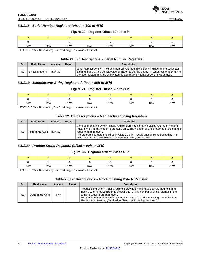
8.5.1.18 Serial Number Registers (offset = 30h to 4Fh)
Figure 20. Register Offset 30h to 4Fh
7 6 5 4 3 2 1 0X X x x x x x x
R/W R/W R/W R/W R/W R/W R/W R/WLEGEND: R/W = Read/Write; R = Read only; –n = value after reset
Table 21. Bit Descriptions – Serial Number RegistersBit Field Name Access Reset Description
7:0 serialNumber[n] RO/RWSerial Number byte N. The serial number returned in the Serial Number string descriptorat string index 1. The default value of these registers is set by TI. When customSernum is1, these registers may be overwritten by EEPROM contents or by an SMBus host.
8.5.1.19 Manufacturer String Registers (offset = 50h to 8Fh)
Figure 21. Register Offset 50h to 8Fh
7 6 5 4 3 2 1 00 0 0 0 0 0 0 0
R/W R/W R/W R/W R/W R/W R/W R/WLEGEND: R/W = Read/Write; R = Read only; –n = value after reset
Table 22. Bit Descriptions – Manufacturer String RegistersBit Field Name Access Reset Description
7:0 mfgStringByte[n] RO/RW
Manufacturer string byte N. These registers provide the string values returned for stringindex 3 when mfgStringLen is greater than 0. The number of bytes returned in the string isequal to mfgStringLen.The programmed data should be in UNICODE UTF-16LE encodings as defined by TheUnicode Standard, Worldwide Character Encoding, Version 5.0.
8.5.1.20 Product String Registers (offset = 90h to CFh)
Figure 22. Register Offset 90h to CFh
7 6 5 4 3 2 1 00 0 0 0 0 0 0 0
R/W R/W R/W R/W R/W R/W R/W R/WLEGEND: R/W = Read/Write; R = Read only; –n = value after reset
Table 23. Bit Descriptions – Product String Byte N RegisterBit Field Name Access Reset Description
7:0 prodStringByte[n] RW
Product string byte N. These registers provide the string values returned for stringindex 2 when prodStringLen is greater than 0. The number of bytes returned in thestring is equal to prodStringLen.The programmed data should be in UNICODE UTF-16LE encodings as defined byThe Unicode Standard, Worldwide Character Encoding, Version 5.0.
23
TUSB8020Bwww.ti.com SLLSEF6C –JULY 2014–REVISED JUNE 2017
Product Folder Links: TUSB8020B
Submit Documentation FeedbackCopyright © 2014–2017, Texas Instruments Incorporated
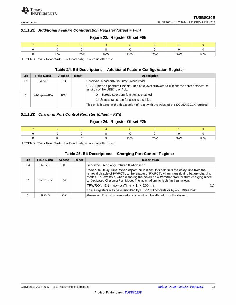
8.5.1.21 Additional Feature Configuration Register (offset = F0h)
Figure 23. Register Offset F0h
7 6 5 4 3 2 1 00 0 0 0 0 0 0 0R R/W R/W R/W R/W R/W R/W R/W
LEGEND: R/W = Read/Write; R = Read only; –n = value after reset
Table 24. Bit Descriptions – Additional Feature Configuration RegisterBit Field Name Access Reset Description7:1 RSVD RO Reserved. Read only, returns 0 when read.
0 usb3spreadDis RW
USB3 Spread Spectrum Disable. This bit allows firmware to disable the spread spectrumfunction of the USB3 phy PLL.
0 = Spread spectrum function is enabled1= Spread spectrum function is disabled
This bit is loaded at the deassertion of reset with the value of the SCL/SMBCLK terminal.
8.5.1.22 Charging Port Control Register (offset = F2h)
Figure 24. Register Offset F2h
7 6 5 4 3 2 1 00 0 0 0 0 0 0 0R R R R R/W R/W R/W R/W
LEGEND: R/W = Read/Write; R = Read only; –n = value after reset
Table 25. Bit Descriptions – Charging Port Control RegisterBit Field Name Access Reset Description7:4 RSVD RO Reserved. Read only, returns 0 when read.
3:1 pwronTime RW
Power-On Delay Time. When dsportEcrEn is set, this field sets the delay time from theremoval disable of PWRCTL to the enable of PWRCTL when transitioning battery chargingmodes. For example, when disabling the power on a transition from custom charging modeto Dedicated Charging Port Mode. The nominal timing is defined as follows:TPWRON_EN = (pwronTime + 1) × 200 ms (1)These registers may be overwritten by EEPROM contents or by an SMBus host.
0 RSVD RW Reserved. This bit is reserved and should not be altered from the default.
24
TUSB8020BSLLSEF6C –JULY 2014–REVISED JUNE 2017 www.ti.com
Product Folder Links: TUSB8020B
Submit Documentation Feedback Copyright © 2014–2017, Texas Instruments Incorporated
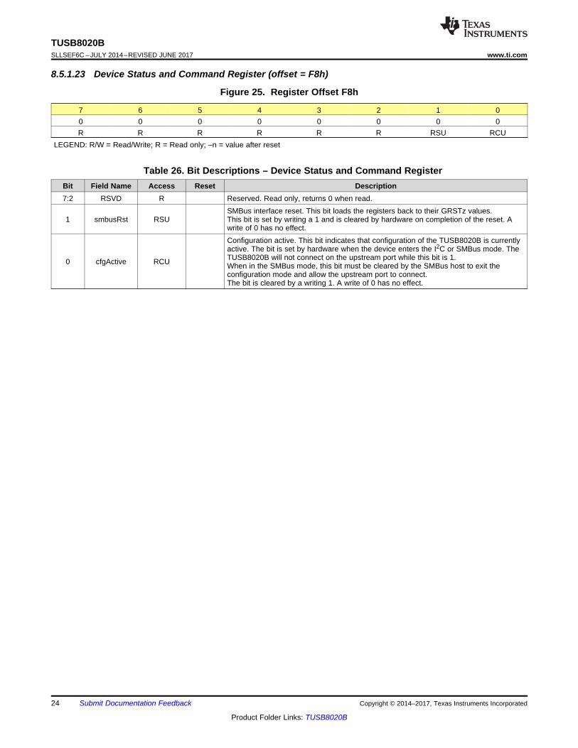
8.5.1.23 Device Status and Command Register (offset = F8h)
Figure 25. Register Offset F8h
7 6 5 4 3 2 1 00 0 0 0 0 0 0 0R R R R R R RSU RCU
LEGEND: R/W = Read/Write; R = Read only; –n = value after reset
Table 26. Bit Descriptions – Device Status and Command RegisterBit Field Name Access Reset Description7:2 RSVD R Reserved. Read only, returns 0 when read.
1 smbusRst RSUSMBus interface reset. This bit loads the registers back to their GRSTz values.This bit is set by writing a 1 and is cleared by hardware on completion of the reset. Awrite of 0 has no effect.
0 cfgActive RCU
Configuration active. This bit indicates that configuration of the TUSB8020B is currentlyactive. The bit is set by hardware when the device enters the I2C or SMBus mode. TheTUSB8020B will not connect on the upstream port while this bit is 1.When in the SMBus mode, this bit must be cleared by the SMBus host to exit theconfiguration mode and allow the upstream port to connect.The bit is cleared by a writing 1. A write of 0 has no effect.
DCPWR
TUSB8020B
USB
Type B
Connector
USB Type A
Connector
USB Type A
Connector
USB
PWR
SWITCH
US Port
DS Port 1 DS Port 2
25
TUSB8020Bwww.ti.com SLLSEF6C –JULY 2014–REVISED JUNE 2017
Product Folder Links: TUSB8020B
Submit Documentation FeedbackCopyright © 2014–2017, Texas Instruments Incorporated
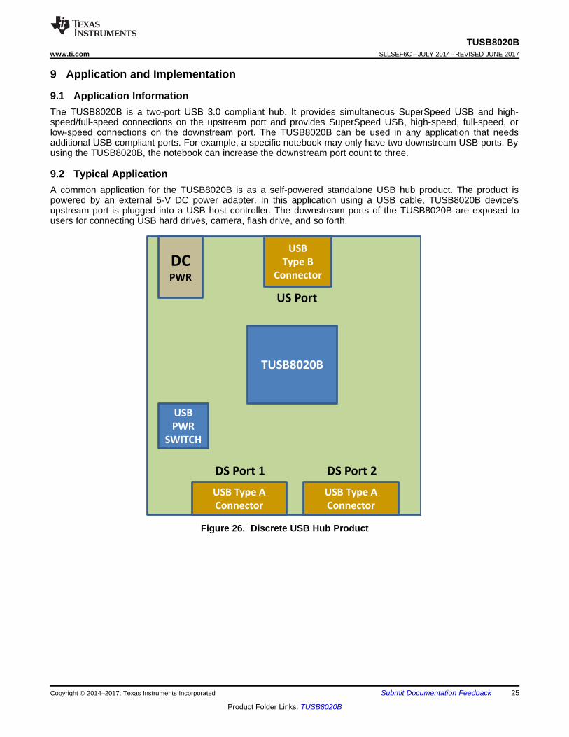
9 Application and Implementation
9.1 Application InformationThe TUSB8020B is a two-port USB 3.0 compliant hub. It provides simultaneous SuperSpeed USB and high-speed/full-speed connections on the upstream port and provides SuperSpeed USB, high-speed, full-speed, orlow-speed connections on the downstream port. The TUSB8020B can be used in any application that needsadditional USB compliant ports. For example, a specific notebook may only have two downstream USB ports. Byusing the TUSB8020B, the notebook can increase the downstream port count to three.
9.2 Typical ApplicationA common application for the TUSB8020B is as a self-powered standalone USB hub product. The product ispowered by an external 5-V DC power adapter. In this application using a USB cable, TUSB8020B device’supstream port is plugged into a USB host controller. The downstream ports of the TUSB8020B are exposed tousers for connecting USB hard drives, camera, flash drive, and so forth.
Figure 26. Discrete USB Hub Product
USB_SSTXP_UP
USB_SSTXM_UP
VBUS
CAP_UP_TXMCAP_UP_TXP
USB_SSRXP_UPUSB_SSRXM_UP
USB_DP_UPUSB_DM_UP
TUSB8020B
U1A
USB_DP_UP26 USB_DM_UP27
USB_SSTXM_UP28
USB_SSTXP_UP29
USB_SSRXM_UP31
USB_SSRXP_UP32
USB_VBUS9
GANGED / SMBA2 / HS_UP35
FULLPWRMGMTZ / SMBA1 / SS_UP36
C110uF
C3 0.1uF 0201
C40.1uF
R3
4.7K
0402
5%
J1
USB3_TYPEB_CONNECTOR
VBUS1
DM2
DP3
GND4
SSTXN5
SSTXP6
GND7
SSRXN8
SSRXP9
SHIELD010
SHIELD111
R5
1M
0402
5%
R4
4.7K
0402
5%
C50.001uF
R210K 1%04021%
R1 90.9K
04021%
C2 0.1uF 0201
Copyright © 2017, Texas Instruments Incorporated
26
TUSB8020BSLLSEF6C –JULY 2014–REVISED JUNE 2017 www.ti.com
Product Folder Links: TUSB8020B
Submit Documentation Feedback Copyright © 2014–2017, Texas Instruments Incorporated
Typical Application (continued)9.2.1 Design Requirements
Table 27. Input ParametersDESIGN PARAMETER EXAMPLE VALUE
VDD supply 1.1 VVDD33 supply 3.3 VUpstream port USB support (SS, HS, FS) SS, HS, FSDownstream port 1 USB support (SS, HS, FS, LS) SS, HS, FS, LSDownstream port 2 USB support (SS, HS, FS, LS) SS, HS, FS, LSNumber of removable downstream ports 2Number of non-removable downstream ports 0Full power management of downstream ports Yes (FULLPWRMGMTZ = 0)Individual control of downstream port power switch Yes (GANGED = 0)Power switch enable polarity Active high (PWRCTL_POL = 0)Battery charge support for downstream port 1 YesBattery charge support for downstream port 2 YesI2C EEPROM support No24-MHz clock source Crystal
9.2.2 Detailed Design Procedure
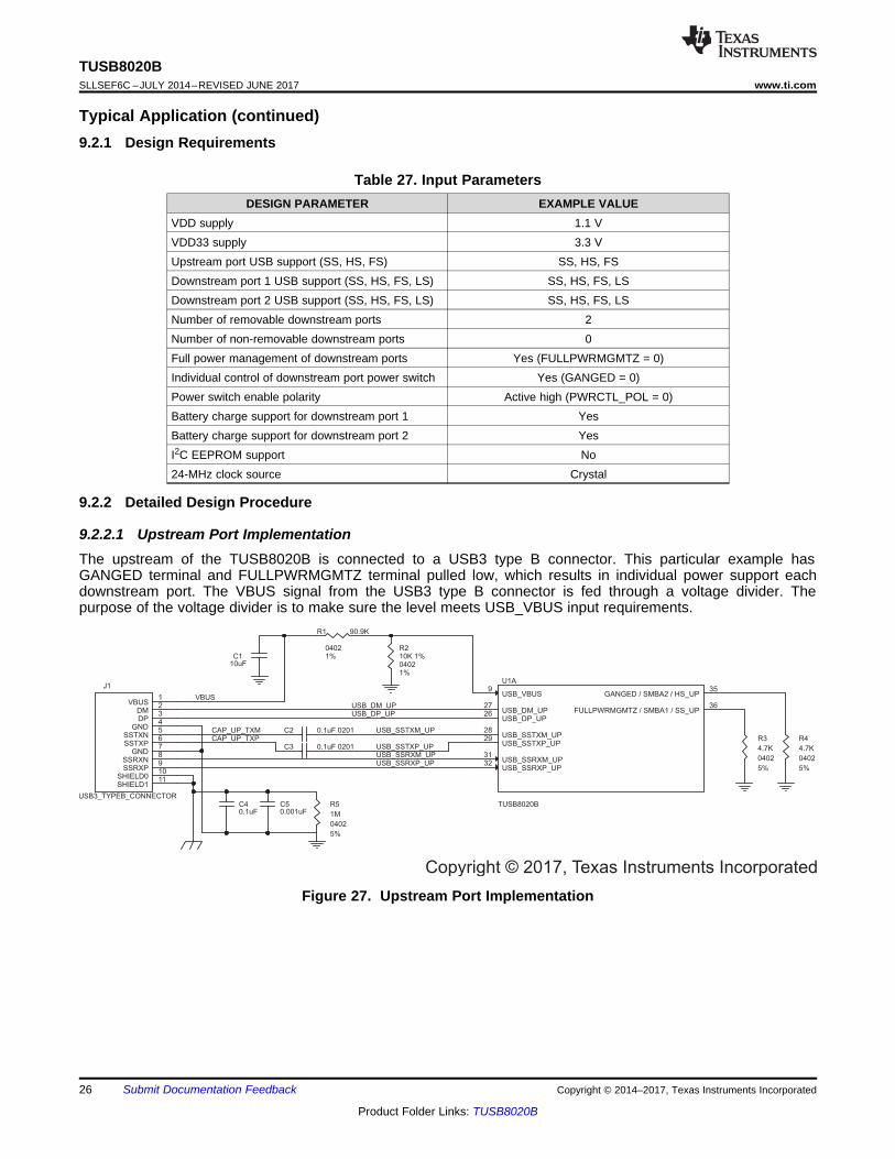
9.2.2.1 Upstream Port ImplementationThe upstream of the TUSB8020B is connected to a USB3 type B connector. This particular example hasGANGED terminal and FULLPWRMGMTZ terminal pulled low, which results in individual power support eachdownstream port. The VBUS signal from the USB3 type B connector is fed through a voltage divider. Thepurpose of the voltage divider is to make sure the level meets USB_VBUS input requirements.
Figure 27. Upstream Port Implementation
POPULATE
FOR BC SUPPORT
USB_SSRXP_DN2USB_SSRXM_DN2
CAP_DN2_TXPCAP_DN2_TXM
VBUS_DS2
USB_DP_DN2USB_DM_DN2
USB_SSTXM_DN2USB_SSTXP_DN2
DN2_VBUS
BOARD_3P3V
DN2_VBUS
OVERCUR2Z
PWRCTRL2_BATEN2
J3
USB3_TYPEA_CONNECTOR
VBUS1
DM2
DP3
GND4
SSRXN5
SSRXP6
GND7
SSTXN8
SSTXP9
SHIELD010
SHIELD111
C110.1uF
C140.1uF
C150.001uF
FB2
220 @ 100MHZ
R10
1M
0402
5%
C13 0.1uF 0201
TUSB8020B
U1C
SMBUSZ / SS_DN222
PWRCTL2 / BATEN26
OVERCUR2Z8
USB_DP_DN214USB_DM_DN215
USB_SSTXP_DN216USB_SSTXM_DN217
USB_SSRXP_DN219USB_SSRXM_DN220
C12 0.1uF 0201
R9
4.7K
0402
5%
Copyright © 2017, Texas Instruments Incorporated
POPULATE
FOR BC SUPPORT
DN1_VBUS VBUS_DS1
USB_SSTXP_DN1
USB_SSRXM_DN1
CAP_DN_TXM1
USB_SSRXP_DN1
CAP_DN_TXP1
USB_DM_DN1USB_DP_DN1
USB_SSTXM_DN1
BOARD_3P3V
DN1_VBUS
PWRCTRL1_BATEN1
OVERCUR1Z
C60.1uF
C90.001uF
C70.1uF 0201
C80.1uF 0201
R7
4.7K
0402
5%
TUSB8020B
U1B
PWRCTL_POL / SS_DN121
USB_DP_DN141USB_DM_DN142
USB_SSTXP_DN143USB_SSTXM_DN144
USB_SSRXP_DN146USB_SSRXM_DN147
PWRCTL1 / BATEN14
OVERCUR1Z5
J2
USB3_TYPEA_CONNECTOR
VBUS1
DM2
DP3
GND4
SSRXN5
SSRXP6
GND7
SSTXN8
SSTXP9
SHIELD010
SHIELD111
C100.1uF
R6
4.7K
0402
5%
FB1
220 @ 100MHZ
R8
1M
0402
5%
Copyright © 2017, Texas Instruments Incorporated
27
TUSB8020Bwww.ti.com SLLSEF6C –JULY 2014–REVISED JUNE 2017
Product Folder Links: TUSB8020B
Submit Documentation FeedbackCopyright © 2014–2017, Texas Instruments Incorporated
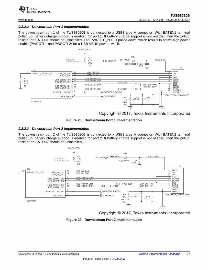
9.2.2.2 Downstream Port 1 ImplementationThe downstream port 1 of the TUSB8020B is connected to a USB3 type A connector. With BATEN1 terminalpulled up, battery charge support is enabled for port 1. If battery charge support is not needed, then the pullupresistor on BATEN1 should be uninstalled. The PWRCTL_POL is pulled-down, which results in active-high powerenable (PWRCTL1 and PWRCTL2) for a USB VBUS power switch.
Figure 28. Downstream Port 1 Implementation
9.2.2.3 Downstream Port 2 ImplementationThe downstream port 2 of the TUSB8020B is connected to a USB3 type A connector. With BATEN2 terminalpulled up, battery charge support is enabled for port 2. If battery charge support is not needed, then the pullupresistor on BATEN2 should be uninstalled.
Figure 29. Downstream Port 2 Implementation
C32
1uF
C34
18pF
R131KTUSB8020B
U1D
XI38
XO39
SCL / SMBCLK2
SDA / SMBDAT3
TEST10
GRSTZ11
USB_R124
R12
9.53K
0402
1%
C33
18pF
Y1
24MHz
R11 1M
Copyright © 2017, Texas Instruments Incorporated
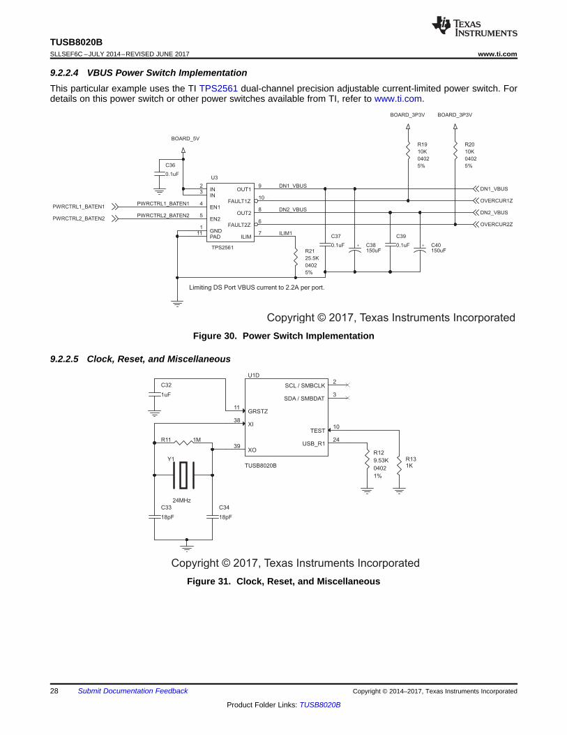
Limiting DS Port VBUS current to 2.2A per port.
PWRCTRL1_BATEN1
PWRCTRL2_BATEN2
ILIM1
DN1_VBUS
DN2_VBUS
BOARD_3P3V
BOARD_5V
BOARD_3P3V
PWRCTRL2_BATEN2DN2_VBUS
DN1_VBUS
PWRCTRL1_BATEN1
OVERCUR2Z
OVERCUR1Z
C36
0.1uF
R19
10K
0402
5%
+ C38150uF
U3
TPS2561
GND1
IN2
IN3
EN14
EN25
FAULT2Z6
ILIM7
OUT28
OUT19
FAULT1Z10
PAD11
C37
0.1uFR21
25.5K
0402
5%
+ C40150uF
C39
0.1uF
R20
10K
0402
5%
Copyright © 2017, Texas Instruments Incorporated
28
TUSB8020BSLLSEF6C –JULY 2014–REVISED JUNE 2017 www.ti.com
Product Folder Links: TUSB8020B
Submit Documentation Feedback Copyright © 2014–2017, Texas Instruments Incorporated
9.2.2.4 VBUS Power Switch ImplementationThis particular example uses the TI TPS2561 dual-channel precision adjustable current-limited power switch. Fordetails on this power switch or other power switches available from TI, refer to www.ti.com.
Figure 30. Power Switch Implementation
9.2.2.5 Clock, Reset, and Miscellaneous
Figure 31. Clock, Reset, and Miscellaneous
VDD11
VDD33
BOARD_3P3V
BOARD_1P1V
C29
0.1uF
C21
0.1uF
C30
0.1uF
C27
0.1uF
C2210uF
C18
0.1uF
C28
0.1uF
C19
0.1uF
C311uF
TUSB8020B
U1E
VDD3325
VD
D3
0
VDD3333
VD
D3
4
VDD3337
VDD3340
VD
D4
5
VDD3348
VD
D1
VDD337
VD
D1
2
VDD3313V
DD
18
VDD3323
TP
AD
49
C23
0.1uF
C16
0.1uF
C25
0.1uF
C24
0.1uF
C17
0.1uF
C26
0.1uF
FB3
220 @ 100MHZC20
0.1uF
FB4
220 @ 100MHZ
Copyright © 2017, Texas Instruments Incorporated
29
TUSB8020Bwww.ti.com SLLSEF6C –JULY 2014–REVISED JUNE 2017
Product Folder Links: TUSB8020B
Submit Documentation FeedbackCopyright © 2014–2017, Texas Instruments Incorporated
9.2.2.6 Power Implementation
Figure 32. Power Implementation
9.2.3 Application Curves
Figure 33. SuperSpeed TX Eye for Downstream Port 1 Figure 34. SuperSpeed TX Eye for Downstream Port 2
Figure 35. HighSpeed TX Eye for Downstream Port 1 Figure 36. HighSpeed TX Eye for Downstream Port 2
30
TUSB8020BSLLSEF6C –JULY 2014–REVISED JUNE 2017 www.ti.com
Product Folder Links: TUSB8020B
Submit Documentation Feedback Copyright © 2014–2017, Texas Instruments Incorporated
10 Power Supply Recommendations
10.1 Power SupplyVDD should be implemented as a single power plane, as should VDD33.• The VDD terminals of the TUSB8020B supply 1.1-V (nominal) power to the core of the TUSB8020B. This
power rail can be isolated from all other power rails by a ferrite bead to reduce noise.• The DC resistance of the ferrite bead on the core power rail can affect the voltage provided to the device due
to the high current draw on the power rail. The output of the core voltage regulator may need to be adjustedto account for this or a ferrite bead with low DC resistance (less than 0.05 Ω) can be selected.
• The VDD33 terminals of the TUSB8020B supply 3.3-V power rail to the I/O of the TUSB8020B. This power railcan be isolated from all other power rails by a ferrite bead to reduce noise.
• All power rails require a 10-µF capacitor or 1-µF capacitors for stability and noise immunity. These bulkcapacitors can be placed anywhere on the power rail. The smaller decoupling capacitors should be placed asclose to the TUSB8020B power pins as possible with an optimal grouping of two of differing values per pin.
10.2 Downstream Port Power• The downstream port power, VBUS, must be supplied by a source capable of supplying 5 V and at least
900 mA per port. Downstream port power switches can be controlled by the TUSB8020BPHP signals. It ispossible to leave the downstream port power always enabled.
• Each downstream port’s VBUS requires a large bulk low-ESR capacitor of 22 µF or larger to limit in-rushcurrent.
• TI recommends ferrite beads on the VBUS pins of the downstream USB port connections for both ESD andEMI reasons. A 0.1-µF capacitor on the USB connector side of the ferrite provides a low-impedance path toground for fast rise time ESD current that might have coupled onto the VBUS trace from the cable.
10.3 GroundTI recommends to use only one board ground plane in the design. This provides the best image plane for signaltraces running above the plane. The thermal pad of the TUSB8020B and any of the voltage regulators should beconnected to this plane with vias. An earth or chassis ground is only implemented near the USB port connectorson a different plane for EMI and ESD purposes.
31
TUSB8020Bwww.ti.com SLLSEF6C –JULY 2014–REVISED JUNE 2017
Product Folder Links: TUSB8020B
Submit Documentation FeedbackCopyright © 2014–2017, Texas Instruments Incorporated
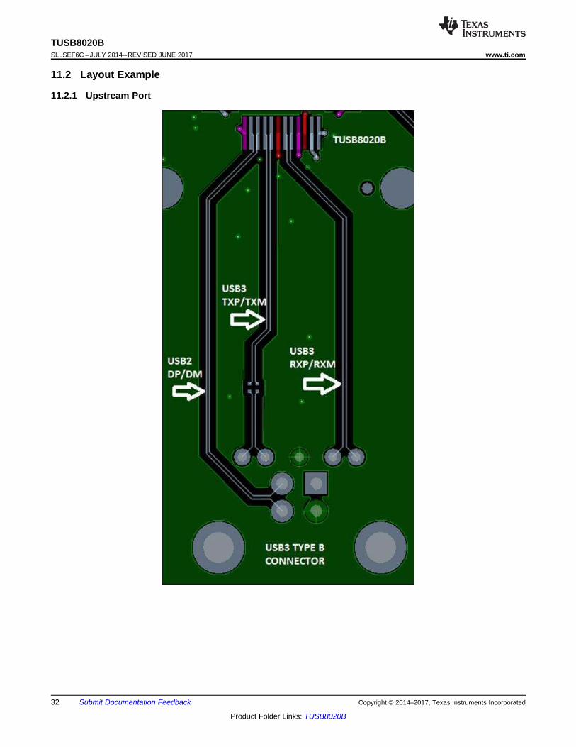
11 Layout
11.1 Layout Guidelines
11.1.1 Placement1. A 9.53-kΩ ±1% resistor connected to terminal USB_R1 should be placed as close as possible to the
TUSB8020B.2. A 0.1-µF capacitor should be placed as close as possible on each VDD and VDD33 power pin.3. The 100-nF capacitors on the SSTXP and SSTXM nets should be placed close to the USB connector (type
A, type B, and so forth).4. The ESD and EMI protection devices (if used) should also be placed as possible to the USB connector.5. If a crystal is used, it must be placed as close as possible to the TUSB8020B device’s XI and XO terminals.6. Place voltage regulators as far away as possible from the TUSB8020B, crystal, and differential pairs.7. In general, the large bulk capacitors associated with each power rail should be placed as close as possible to
the voltage regulators.
11.1.2 Package Specific1. The TUSB8020B package has a 0.5-mm pin pitch.2. The TUSB8020B package has a 3.6-mm × 3.6-mm thermal pad. This thermal pad must be connected to
ground through a system of vias.3. All vias under device, except for those connected to thermal pad, should be solder masked to avoid potential
issues with thermal pad layouts.
11.1.3 Differential PairsThis section describes the layout recommendations for all of the TUSB8020B differential pairs: USB_DP_XX,USB_DM_XX, USB_SSTXP_XX, USB_SSTXM_XX, USB_SSRXP_XX, and USB_SSRXM_XX.• Must be designed with a differential impedance of 90 Ω ±10%.• To minimize crosstalk, TI recommends to keep high-speed signals away from each other. Each pair should
be separated by at least 5× the signal trace width. Separating with ground as depicted in the layout examplealso helps minimize crosstalk.
• Route all differential pairs on the same layer adjacent to a solid ground plane.• Do not route differential pairs over any plane split.• Adding test points causes impedance discontinuity, and therefore, negatively impacts signal performance. If
test points are used, they should be placed in series and symmetrically. They must not be placed in a mannerthat causes stub on the differential pair.
• Avoid 90° turns in trace. The use of bends in differential traces should be kept to a minimum. When bendsare used, the number of left and right bends should be as equal as possible and the angle of the bend shouldbe ≥135°. Taking this action minimizes any length mismatch caused by the bends, and therefore, minimizesthe impact bends have on EMI.
• Minimize the trace lengths of the differential pair traces. Eight inches is the maximum recommended tracelength for SS differential-pair signals and USB 2.0 differential-pair signals. Longer trace lengths require verycareful routing to assure proper signal integrity.
• Match the etch lengths of the differential pair traces (that is DP and DM or SSRXP and SSRXM or SSTXPand SSTXM). There should be less than 5-mils difference between a SS differential-pair signal and itscomplement. The USB 2.0 differential pairs should not exceed 50-mils relative trace length difference.
• The etch lengths of the differential pair groups do not need to match (that is the length of the SSRX pair tothat of the SSTX pair), but all trace lengths should be minimized.
• Minimize the use of vias in the differential-pair paths as much as possible. If this is not practical, ensure thatthe same via type and placement are used for both signals in a pair. Any vias used should be placed as closeas possible to the TUSB8020B device.
• To ease routing, the polarity of the SS differential pairs can be swapped. This means that SSTXP can berouted to SSTXM or SSRXM can be routed to SSRXP.
• Do not place power fuses across the differential-pair traces.
32
TUSB8020BSLLSEF6C –JULY 2014–REVISED JUNE 2017 www.ti.com
Product Folder Links: TUSB8020B
Submit Documentation Feedback Copyright © 2014–2017, Texas Instruments Incorporated
11.2 Layout Example
11.2.1 Upstream Port
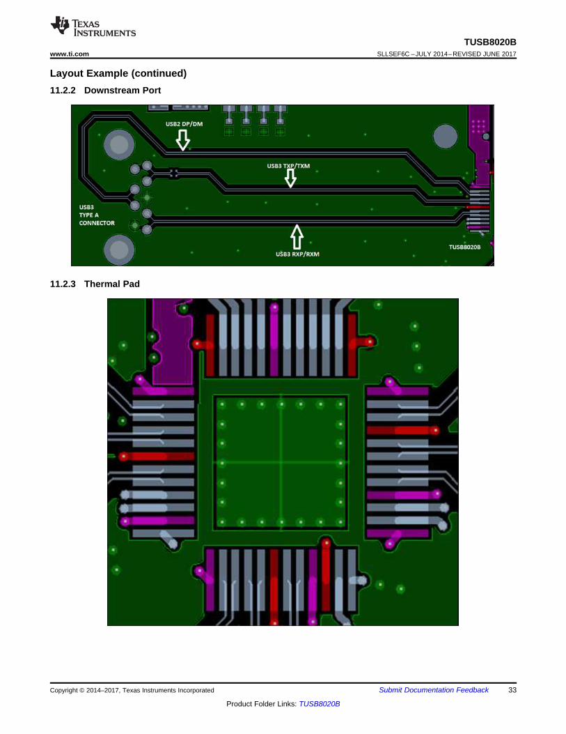
33
TUSB8020Bwww.ti.com SLLSEF6C –JULY 2014–REVISED JUNE 2017
Product Folder Links: TUSB8020B
Submit Documentation FeedbackCopyright © 2014–2017, Texas Instruments Incorporated
Layout Example (continued)11.2.2 Downstream Port
11.2.3 Thermal Pad
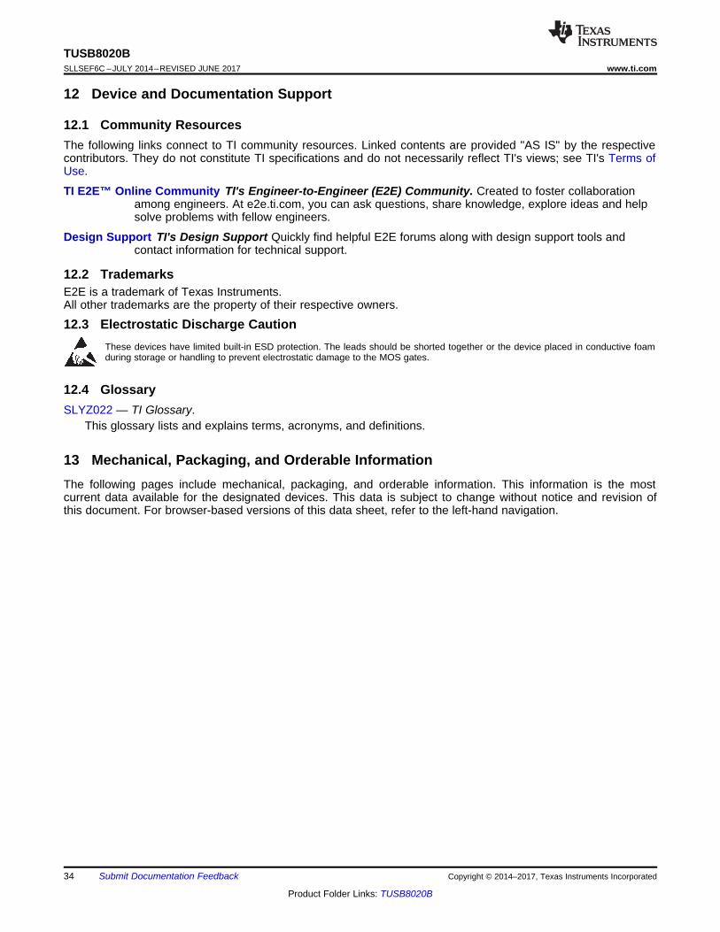
34
TUSB8020BSLLSEF6C –JULY 2014–REVISED JUNE 2017 www.ti.com
Product Folder Links: TUSB8020B
Submit Documentation Feedback Copyright © 2014–2017, Texas Instruments Incorporated
12 Device and Documentation Support
12.1 Community ResourcesThe following links connect to TI community resources. Linked contents are provided "AS IS" by the respectivecontributors. They do not constitute TI specifications and do not necessarily reflect TI's views; see TI's Terms ofUse.
TI E2E™ Online Community TI's Engineer-to-Engineer (E2E) Community. Created to foster collaborationamong engineers. At e2e.ti.com, you can ask questions, share knowledge, explore ideas and helpsolve problems with fellow engineers.
Design Support TI's Design Support Quickly find helpful E2E forums along with design support tools andcontact information for technical support.
12.2 TrademarksE2E is a trademark of Texas Instruments.All other trademarks are the property of their respective owners.
12.3 Electrostatic Discharge CautionThese devices have limited built-in ESD protection. The leads should be shorted together or the device placed in conductive foamduring storage or handling to prevent electrostatic damage to the MOS gates.
12.4 GlossarySLYZ022 — TI Glossary.
This glossary lists and explains terms, acronyms, and definitions.
13 Mechanical, Packaging, and Orderable InformationThe following pages include mechanical, packaging, and orderable information. This information is the mostcurrent data available for the designated devices. This data is subject to change without notice and revision ofthis document. For browser-based versions of this data sheet, refer to the left-hand navigation.
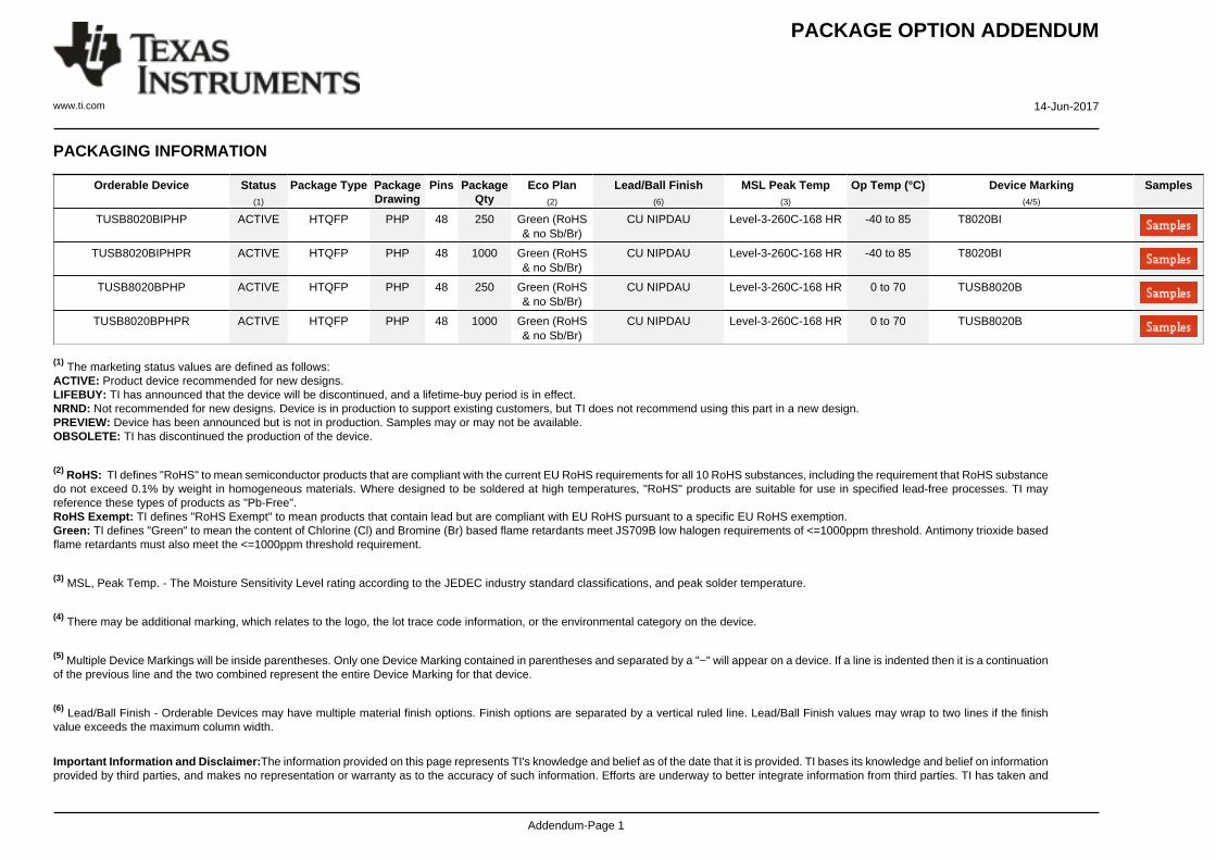
PACKAGE OPTION ADDENDUM
www.ti.com 14-Jun-2017
Addendum-Page 1
PACKAGING INFORMATION
Orderable Device Status(1)
Package Type PackageDrawing
Pins PackageQty
Eco Plan(2)
Lead/Ball Finish(6)
MSL Peak Temp(3)
Op Temp (°C) Device Marking(4/5)
Samples
TUSB8020BIPHP ACTIVE HTQFP PHP 48 250 Green (RoHS& no Sb/Br)
CU NIPDAU Level-3-260C-168 HR -40 to 85 T8020BI
TUSB8020BIPHPR ACTIVE HTQFP PHP 48 1000 Green (RoHS& no Sb/Br)
CU NIPDAU Level-3-260C-168 HR -40 to 85 T8020BI
TUSB8020BPHP ACTIVE HTQFP PHP 48 250 Green (RoHS& no Sb/Br)
CU NIPDAU Level-3-260C-168 HR 0 to 70 TUSB8020B
TUSB8020BPHPR ACTIVE HTQFP PHP 48 1000 Green (RoHS& no Sb/Br)
CU NIPDAU Level-3-260C-168 HR 0 to 70 TUSB8020B
(1) The marketing status values are defined as follows:ACTIVE: Product device recommended for new designs.LIFEBUY: TI has announced that the device will be discontinued, and a lifetime-buy period is in effect.NRND: Not recommended for new designs. Device is in production to support existing customers, but TI does not recommend using this part in a new design.PREVIEW: Device has been announced but is not in production. Samples may or may not be available.OBSOLETE: TI has discontinued the production of the device.
(2) RoHS: TI defines "RoHS" to mean semiconductor products that are compliant with the current EU RoHS requirements for all 10 RoHS substances, including the requirement that RoHS substancedo not exceed 0.1% by weight in homogeneous materials. Where designed to be soldered at high temperatures, "RoHS" products are suitable for use in specified lead-free processes. TI mayreference these types of products as "Pb-Free".RoHS Exempt: TI defines "RoHS Exempt" to mean products that contain lead but are compliant with EU RoHS pursuant to a specific EU RoHS exemption.Green: TI defines "Green" to mean the content of Chlorine (Cl) and Bromine (Br) based flame retardants meet JS709B low halogen requirements of <=1000ppm threshold. Antimony trioxide basedflame retardants must also meet the <=1000ppm threshold requirement.
(3) MSL, Peak Temp. - The Moisture Sensitivity Level rating according to the JEDEC industry standard classifications, and peak solder temperature.
(4) There may be additional marking, which relates to the logo, the lot trace code information, or the environmental category on the device.
(5) Multiple Device Markings will be inside parentheses. Only one Device Marking contained in parentheses and separated by a "~" will appear on a device. If a line is indented then it is a continuationof the previous line and the two combined represent the entire Device Marking for that device.
(6) Lead/Ball Finish - Orderable Devices may have multiple material finish options. Finish options are separated by a vertical ruled line. Lead/Ball Finish values may wrap to two lines if the finishvalue exceeds the maximum column width.
Important Information and Disclaimer:The information provided on this page represents TI's knowledge and belief as of the date that it is provided. TI bases its knowledge and belief on informationprovided by third parties, and makes no representation or warranty as to the accuracy of such information. Efforts are underway to better integrate information from third parties. TI has taken and
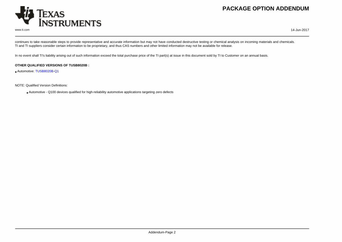
PACKAGE OPTION ADDENDUM
www.ti.com 14-Jun-2017
Addendum-Page 2
continues to take reasonable steps to provide representative and accurate information but may not have conducted destructive testing or chemical analysis on incoming materials and chemicals.TI and TI suppliers consider certain information to be proprietary, and thus CAS numbers and other limited information may not be available for release.
In no event shall TI's liability arising out of such information exceed the total purchase price of the TI part(s) at issue in this document sold by TI to Customer on an annual basis.
OTHER QUALIFIED VERSIONS OF TUSB8020B :
• Automotive: TUSB8020B-Q1
NOTE: Qualified Version Definitions:
• Automotive - Q100 devices qualified for high-reliability automotive applications targeting zero defects
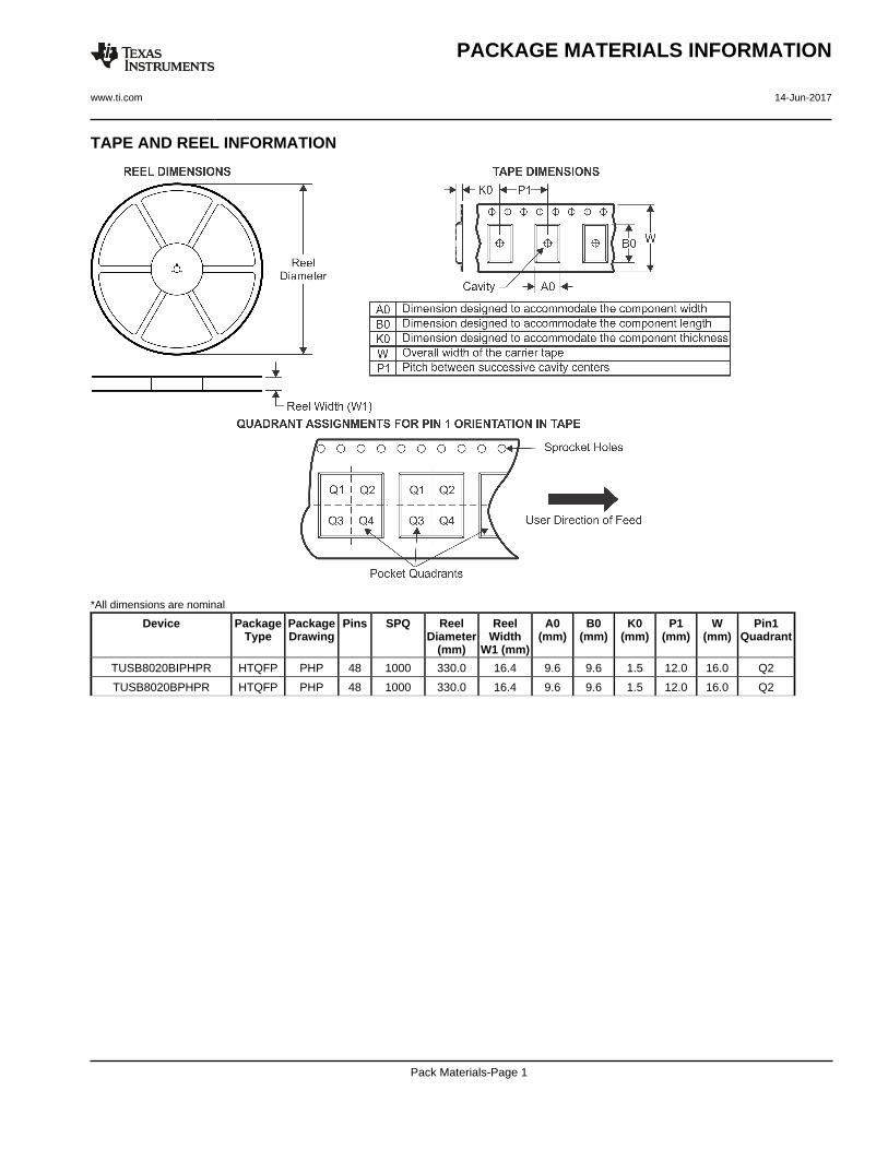
TAPE AND REEL INFORMATION
*All dimensions are nominal
Device PackageType
PackageDrawing
Pins SPQ ReelDiameter
(mm)
ReelWidth
W1 (mm)
A0(mm)
B0(mm)
K0(mm)
P1(mm)
W(mm)
Pin1Quadrant
TUSB8020BIPHPR HTQFP PHP 48 1000 330.0 16.4 9.6 9.6 1.5 12.0 16.0 Q2
TUSB8020BPHPR HTQFP PHP 48 1000 330.0 16.4 9.6 9.6 1.5 12.0 16.0 Q2
PACKAGE MATERIALS INFORMATION
www.ti.com 14-Jun-2017
Pack Materials-Page 1
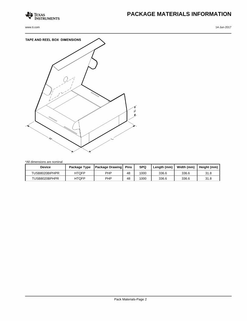
*All dimensions are nominal
Device Package Type Package Drawing Pins SPQ Length (mm) Width (mm) Height (mm)
TUSB8020BIPHPR HTQFP PHP 48 1000 336.6 336.6 31.8
TUSB8020BPHPR HTQFP PHP 48 1000 336.6 336.6 31.8
PACKAGE MATERIALS INFORMATION
www.ti.com 14-Jun-2017
Pack Materials-Page 2
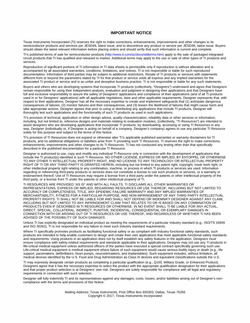
IMPORTANT NOTICE
Texas Instruments Incorporated (TI) reserves the right to make corrections, enhancements, improvements and other changes to itssemiconductor products and services per JESD46, latest issue, and to discontinue any product or service per JESD48, latest issue. Buyersshould obtain the latest relevant information before placing orders and should verify that such information is current and complete.TI’s published terms of sale for semiconductor products (http://www.ti.com/sc/docs/stdterms.htm) apply to the sale of packaged integratedcircuit products that TI has qualified and released to market. Additional terms may apply to the use or sale of other types of TI products andservices.Reproduction of significant portions of TI information in TI data sheets is permissible only if reproduction is without alteration and isaccompanied by all associated warranties, conditions, limitations, and notices. TI is not responsible or liable for such reproduceddocumentation. Information of third parties may be subject to additional restrictions. Resale of TI products or services with statementsdifferent from or beyond the parameters stated by TI for that product or service voids all express and any implied warranties for theassociated TI product or service and is an unfair and deceptive business practice. TI is not responsible or liable for any such statements.Buyers and others who are developing systems that incorporate TI products (collectively, “Designers”) understand and agree that Designersremain responsible for using their independent analysis, evaluation and judgment in designing their applications and that Designers havefull and exclusive responsibility to assure the safety of Designers' applications and compliance of their applications (and of all TI productsused in or for Designers’ applications) with all applicable regulations, laws and other applicable requirements. Designer represents that, withrespect to their applications, Designer has all the necessary expertise to create and implement safeguards that (1) anticipate dangerousconsequences of failures, (2) monitor failures and their consequences, and (3) lessen the likelihood of failures that might cause harm andtake appropriate actions. Designer agrees that prior to using or distributing any applications that include TI products, Designer willthoroughly test such applications and the functionality of such TI products as used in such applications.TI’s provision of technical, application or other design advice, quality characterization, reliability data or other services or information,including, but not limited to, reference designs and materials relating to evaluation modules, (collectively, “TI Resources”) are intended toassist designers who are developing applications that incorporate TI products; by downloading, accessing or using TI Resources in anyway, Designer (individually or, if Designer is acting on behalf of a company, Designer’s company) agrees to use any particular TI Resourcesolely for this purpose and subject to the terms of this Notice.TI’s provision of TI Resources does not expand or otherwise alter TI’s applicable published warranties or warranty disclaimers for TIproducts, and no additional obligations or liabilities arise from TI providing such TI Resources. TI reserves the right to make corrections,enhancements, improvements and other changes to its TI Resources. TI has not conducted any testing other than that specificallydescribed in the published documentation for a particular TI Resource.Designer is authorized to use, copy and modify any individual TI Resource only in connection with the development of applications thatinclude the TI product(s) identified in such TI Resource. NO OTHER LICENSE, EXPRESS OR IMPLIED, BY ESTOPPEL OR OTHERWISETO ANY OTHER TI INTELLECTUAL PROPERTY RIGHT, AND NO LICENSE TO ANY TECHNOLOGY OR INTELLECTUAL PROPERTYRIGHT OF TI OR ANY THIRD PARTY IS GRANTED HEREIN, including but not limited to any patent right, copyright, mask work right, orother intellectual property right relating to any combination, machine, or process in which TI products or services are used. Informationregarding or referencing third-party products or services does not constitute a license to use such products or services, or a warranty orendorsement thereof. Use of TI Resources may require a license from a third party under the patents or other intellectual property of thethird party, or a license from TI under the patents or other intellectual property of TI.TI RESOURCES ARE PROVIDED “AS IS” AND WITH ALL FAULTS. TI DISCLAIMS ALL OTHER WARRANTIES ORREPRESENTATIONS, EXPRESS OR IMPLIED, REGARDING RESOURCES OR USE THEREOF, INCLUDING BUT NOT LIMITED TOACCURACY OR COMPLETENESS, TITLE, ANY EPIDEMIC FAILURE WARRANTY AND ANY IMPLIED WARRANTIES OFMERCHANTABILITY, FITNESS FOR A PARTICULAR PURPOSE, AND NON-INFRINGEMENT OF ANY THIRD PARTY INTELLECTUALPROPERTY RIGHTS. TI SHALL NOT BE LIABLE FOR AND SHALL NOT DEFEND OR INDEMNIFY DESIGNER AGAINST ANY CLAIM,INCLUDING BUT NOT LIMITED TO ANY INFRINGEMENT CLAIM THAT RELATES TO OR IS BASED ON ANY COMBINATION OFPRODUCTS EVEN IF DESCRIBED IN TI RESOURCES OR OTHERWISE. IN NO EVENT SHALL TI BE LIABLE FOR ANY ACTUAL,DIRECT, SPECIAL, COLLATERAL, INDIRECT, PUNITIVE, INCIDENTAL, CONSEQUENTIAL OR EXEMPLARY DAMAGES INCONNECTION WITH OR ARISING OUT OF TI RESOURCES OR USE THEREOF, AND REGARDLESS OF WHETHER TI HAS BEENADVISED OF THE POSSIBILITY OF SUCH DAMAGES.Unless TI has explicitly designated an individual product as meeting the requirements of a particular industry standard (e.g., ISO/TS 16949and ISO 26262), TI is not responsible for any failure to meet such industry standard requirements.Where TI specifically promotes products as facilitating functional safety or as compliant with industry functional safety standards, suchproducts are intended to help enable customers to design and create their own applications that meet applicable functional safety standardsand requirements. Using products in an application does not by itself establish any safety features in the application. Designers mustensure compliance with safety-related requirements and standards applicable to their applications. Designer may not use any TI products inlife-critical medical equipment unless authorized officers of the parties have executed a special contract specifically governing such use.Life-critical medical equipment is medical equipment where failure of such equipment would cause serious bodily injury or death (e.g., lifesupport, pacemakers, defibrillators, heart pumps, neurostimulators, and implantables). Such equipment includes, without limitation, allmedical devices identified by the U.S. Food and Drug Administration as Class III devices and equivalent classifications outside the U.S.TI may expressly designate certain products as completing a particular qualification (e.g., Q100, Military Grade, or Enhanced Product).Designers agree that it has the necessary expertise to select the product with the appropriate qualification designation for their applicationsand that proper product selection is at Designers’ own risk. Designers are solely responsible for compliance with all legal and regulatoryrequirements in connection with such selection.Designer will fully indemnify TI and its representatives against any damages, costs, losses, and/or liabilities arising out of Designer’s non-compliance with the terms and provisions of this Notice.
Mailing Address: Texas Instruments, Post Office Box 655303, Dallas, Texas 75265Copyright © 2017, Texas Instruments Incorporated